1
ZPUino User Manual
Alvaro Lopes
April 10, 2012
Contents
1 Version
4
2 ZPUino
5
2.0.1 What is inside ZPUino
2.0.2 Where does it run . . .
2.0.3 IO Device features . .
2.0.4 Hardware support . . .
2.1 Overview . . . . . . . . . . . .
3 Peripheral Pin Select
3.1 Redirecting output
3.1.1 Examples .
3.2 Redirecting input .
3.2.1 Examples .
.
.
.
.
.
.
.
.
.
.
.
.
.
.
.
.
.
.
.
.
.
.
.
.
.
.
.
.
.
.
.
.
.
.
.
.
.
.
.
.
.
.
.
.
.
.
.
.
.
.
.
.
.
.
.
.
.
.
.
.
.
.
.
.
.
.
.
.
.
.
.
.
.
.
.
.
.
.
.
.
.
.
.
.
.
.
.
.
.
.
.
.
.
.
.
.
.
.
.
.
.
.
.
.
.
.
.
.
.
.
.
.
.
.
.
.
.
.
.
.
.
.
.
.
.
.
.
.
.
.
.
.
.
.
.
.
.
.
.
.
.
.
.
.
.
.
.
.
.
.
.
.
5
5
6
7
8
9
.
.
.
.
.
.
.
.
.
.
.
.
.
.
.
.
.
.
.
.
.
.
.
.
.
.
.
.
.
.
.
.
.
.
.
.
.
.
.
.
.
.
.
.
.
.
.
.
.
.
.
.
.
.
.
.
.
.
.
.
.
.
.
.
.
.
.
.
.
.
.
.
.
.
.
.
.
.
.
.
.
.
.
.
. 9
. 9
. 10
. 10
4.1 GPIO . . . . . . . . . . . . . . . .
4.1.1 HDL sources and modules .
4.1.2 Location . . . . . . . . . . .
4.1.3 Registers . . . . . . . . . . .
4.1.4 Software . . . . . . . . . . .
4.2 Timers . . . . . . . . . . . . . . . .
4.2.1 HDL sources and modules .
4.2.2 Location . . . . . . . . . . .
4.2.3 Registers . . . . . . . . . . .
4.2.4 PWM registers . . . . . . .
4.2.5 Timer prescaler . . . . . . .
4.2.6 Timer PWM update policy
4.2.7 Software . . . . . . . . . . .
4.3 UART . . . . . . . . . . . . . . . .
4.3.1 HDL sources and modules .
4.3.2 Location . . . . . . . . . . .
4.3.3 Registers . . . . . . . . . . .
4.3.4 UART Prescaler . . . . . . .
4.3.5 Software . . . . . . . . . . .
.
.
.
.
.
.
.
.
.
.
.
.
.
.
.
.
.
.
.
.
.
.
.
.
.
.
.
.
.
.
.
.
.
.
.
.
.
.
.
.
.
.
.
.
.
.
.
.
.
.
.
.
.
.
.
.
.
.
.
.
.
.
.
.
.
.
.
.
.
.
.
.
.
.
.
.
.
.
.
.
.
.
.
.
.
.
.
.
.
.
.
.
.
.
.
.
.
.
.
.
.
.
.
.
.
.
.
.
.
.
.
.
.
.
.
.
.
.
.
.
.
.
.
.
.
.
.
.
.
.
.
.
.
.
.
.
.
.
.
.
.
.
.
.
.
.
.
.
.
.
.
.
.
.
.
.
.
.
.
.
.
.
.
.
.
.
.
.
.
.
.
.
.
.
.
.
.
.
.
.
.
.
.
.
.
.
.
.
.
.
.
.
.
.
.
.
.
.
.
.
.
.
.
.
.
.
.
.
.
.
.
.
.
.
.
.
.
.
.
.
.
.
.
.
.
.
.
.
.
.
.
.
.
.
.
.
.
.
.
.
.
.
.
.
.
.
.
.
.
.
.
.
.
.
.
.
.
.
.
.
.
.
.
.
.
.
.
.
.
.
.
.
.
.
.
.
.
.
.
.
.
.
.
.
.
.
.
.
.
.
.
.
.
.
.
.
.
.
.
.
.
.
.
.
.
.
.
.
.
.
.
.
.
.
.
.
.
.
.
.
.
.
.
.
.
.
.
.
.
.
.
.
.
.
.
.
.
.
.
.
.
.
.
.
.
.
.
.
.
.
.
.
.
.
.
.
.
.
.
.
.
.
.
.
.
.
.
.
.
.
.
.
.
.
.
.
.
.
.
.
.
.
.
.
.
.
.
.
.
.
.
.
.
.
.
.
.
.
.
4 IO Modules
2
11
12
12
13
13
14
15
15
16
16
18
19
19
20
22
22
23
23
24
25
4.4 CRC16 . . . . . . . . . . . . . . .
4.4.1 HDL sources and modules
4.4.2 Location . . . . . . . . . .
4.4.3 Registers . . . . . . . . . .
4.4.4 Software . . . . . . . . . .
4.5 Interrupt Controller . . . . . . . .
4.5.1 HDL sources and modules
4.5.2 Location . . . . . . . . . .
4.5.3 Registers . . . . . . . . . .
4.5.4 Software . . . . . . . . . .
4.6 SigmaDelta DAC . . . . . . . . .
4.6.1 HDL sources and modules
4.6.2 Location . . . . . . . . . .
4.6.3 Registers . . . . . . . . . .
4.6.4 Software . . . . . . . . . .
4.7 SPI . . . . . . . . . . . . . . . . .
4.7.1 HDL sources and modules
4.7.2 Location . . . . . . . . . .
4.7.3 Registers . . . . . . . . . .
4.7.4 SPI clock prescaler . . . .
4.7.5 Software . . . . . . . . . .
.
.
.
.
.
.
.
.
.
.
.
.
.
.
.
.
.
.
.
.
.
.
.
.
.
.
.
.
.
.
.
.
.
.
.
.
.
.
.
.
.
.
.
.
.
.
.
.
.
.
.
.
.
.
.
.
.
.
.
.
.
.
.
.
.
.
.
.
.
.
.
.
.
.
.
.
.
.
.
.
.
.
.
.
.
.
.
.
.
.
.
.
.
.
.
.
.
.
.
.
.
.
.
.
.
.
.
.
.
.
.
.
.
.
.
.
.
.
.
.
.
.
.
.
.
.
.
.
.
.
.
.
.
.
.
.
.
.
.
.
.
.
.
.
.
.
.
.
.
.
.
.
.
.
.
.
.
.
.
.
.
.
.
.
.
.
.
.
.
.
.
.
.
.
.
.
.
.
.
.
.
.
.
.
.
.
.
.
.
.
.
.
.
.
.
.
.
.
.
.
.
.
.
.
.
.
.
.
.
.
.
.
.
.
.
.
.
.
.
.
.
.
.
.
.
.
.
.
.
.
.
.
.
.
.
.
.
.
.
.
.
.
.
.
.
.
.
.
.
.
.
.
.
.
.
.
.
.
.
.
.
.
.
.
.
.
.
.
.
.
.
.
.
.
.
.
.
.
.
.
.
.
.
.
.
.
.
.
.
.
.
.
.
.
.
.
.
.
.
.
.
.
.
.
.
.
.
.
.
.
.
.
.
.
.
.
.
.
.
.
.
.
.
.
.
.
.
.
.
.
.
.
.
.
.
.
.
.
.
.
.
.
.
.
.
.
.
.
.
.
.
.
.
.
.
.
.
.
.
.
.
.
.
.
.
.
.
.
.
.
.
.
.
.
.
.
.
.
.
.
.
.
.
.
.
.
.
.
.
.
.
.
.
.
.
.
.
.
.
.
.
.
.
.
.
.
.
.
.
.
.
.
.
.
.
.
.
.
.
.
.
.
.
.
.
.
.
.
.
.
.
.
.
.
.
.
.
.
.
.
.
.
.
.
.
.
.
.
.
.
.
.
.
.
.
.
.
.
.
.
.
.
5.1 SmallFS library . . . . . . . . . . . .
5.1.1 What is SmallFS ? . . . . . .
5.1.2 Advantages and disadvantages
5.1.3 Technical details . . . . . . .
5.1.4 The library . . . . . . . . . .
5.1.5 Tools . . . . . . . . . . . . . .
5.1.6 Integration . . . . . . . . . .
.
.
.
.
.
.
.
.
.
.
.
.
.
.
.
.
.
.
.
.
.
.
.
.
.
.
.
.
.
.
.
.
.
.
.
.
.
.
.
.
.
.
.
.
.
.
.
.
.
.
.
.
.
.
.
.
.
.
.
.
.
.
.
.
.
.
.
.
.
.
.
.
.
.
.
.
.
.
.
.
.
.
.
.
.
.
.
.
.
.
.
.
.
.
.
.
.
.
.
.
.
.
.
.
.
.
.
.
.
.
.
.
.
.
.
.
.
.
.
.
.
.
.
.
.
.
.
.
.
.
.
.
.
.
.
.
.
.
.
.
.
.
.
.
.
.
.
.
.
.
.
.
.
.
.
.
.
.
.
.
.
.
.
.
.
.
.
.
.
.
.
.
.
.
.
.
.
.
.
.
.
.
.
.
.
.
.
.
.
.
.
.
.
.
.
.
.
.
.
.
.
.
.
.
.
.
.
.
.
.
.
.
.
.
.
.
.
.
.
.
.
.
.
.
.
.
.
.
.
.
.
.
.
.
.
.
.
.
.
.
5 Libraries
6 Boards
6.1 Interpreting board information .
6.1.1 Pin mappings and PPS .
6.2 Gadget Factory Papilio One 250
6.3 Gadget Factory Papilio One 500
6.4 Spartan3E Starter Kit (S3E500)
.
.
.
.
.
.
.
.
.
.
7 Legal information
.
.
.
.
.
26
26
26
26
28
30
30
30
30
31
32
32
32
33
34
35
35
35
35
36
37
38
39
39
39
39
40
41
41
42
42
42
44
47
51
55
7.1 Licensing . . . . . . . . . . . . . . . . . . . . . . . . . . . . . . . . . . . . 55
7.2 Disclaimer . . . . . . . . . . . . . . . . . . . . . . . . . . . . . . . . . . . 55
3
1 Version
This is version 0.9 of the document.
4
2 ZPUino
ZPUino is a SoC (System-on-a-Chip) based on Zylin's ZPU 32-bit processor core.
2.0.1 What is inside ZPUino
Hardware-wise, ZPUino currently integrates the following devices:
• ZPU Extreme Core, a modied ZPU core
• One or two UART
• Two SPI interfaces
• A 16-bit and a 24-bit timer.
• One TSC (Time Stamp Counter)
• 128-bit GPIO interface
• Interrupt Controller
• Two SigmaDelta outputs
• Peripheral Pin Select
• VGA (optional)
Software-wise, it supports the following features:
• 4Kb Bootloader, which includes required emulation code for ZPU.
• Bootstraps code from program ash (shadows into FPGA blockram)
• Serial programming of program ash.
2.0.2 Where does it run
First implementation was done on Spartan3E 500 (-4), on a S3E Starter Kit, with a
M25P16 SPI ash ROM and 32Kbytes RAM.
Right now it runs on other many boards, see chapter ?? for more information.
unning speed: up to 100MHz, 96MHz recommended.
5
2.0.3 IO Device features
UART features:
• 16-bit prescaler
• 2048-byte deep receive FIFO. (16 byte in reduced implementations)
SPI features:
• Two independent SPI master controllers
• Programmable prescaler
• Congurable CPOL
• Congurable SRE (Sample on Rising Edge)
• 8, 16, 24 and 32-bit transmission modes, 4 byte (32 bit) receive register.
• Congurable blocking operation
Timer features:
• Two independent timers
• 10-bit prescaler
• 16-bit and 24-bit counter
• Count-up and Count-down mode
• 16-bit Compare register
• Clear on Compare match support
• Interrupt support on Compare Match
• Output compare Registers to GPIO pin (allows PWM)
GPIO features:
• Up to 128 GPIO entries
• Bi-directional (tristate) conguration
SigmaDelta features:
• Two 16-bit channel
• Runs at system clock speed
• Congurable endianness
PPS (Peripheral pin select) features:
• Map every device pin to any GPIO pin
• Fully congurable in run-time
6
VGA features:
• HQVGA (160x120), using 800x600@75Hz output.
• 8-bit color (3 bits red, 3 bits green, 2 bits blue).
• Integrated programable character ram (8x8)
ZPUino programmer:
• 1Mbps programming speed
• Supports programming both sketches and FPGA bitle [if ZPUino bootloader
already loaded]
• Support for upload-to-ram
2.0.4 Hardware support
Currently ZPUino should run on any Spartan3E FPGA (from 250 and beyond), and
Spartan6 FPGA (LX4 and beyond).
List of ash devices currently supported by programmer:
• ST M25P16
• SST SST25VF040B
• ATMEL AT45DB081D
Other ash might be supported. Specically ash from same series, but with dierent
capacities, can be easily added to programmer. For other ash vendors or models contact
us by e-mail.
7
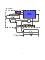
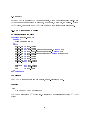
2.1 Overview
8
3 Peripheral Pin Select
This information relates to ZPUino 1.0 release. Other releases might have dierent specs.
ZPUino includes a feature which is called Peripheral Pin Select (in short, PPS). PPS
allows you to map every device input or output pin (such as SPI clock and SPI data
lines) to each individual pin (GPIO), thus not requiring you to perform synthesis and
P&R each time you want to use a device on a dierent IO pin.
To simplify things, three methods are supplied to manipulate PPS:
void pinModePPS ( int pin , int value );
void outputPinForFunction ( unsigned int pin , unsigned int function );
void inputPinForFunction ( unsigned int pin , unsigned int function );
Three register blocks exist to congure how pin selection is done. These are called
GP IOP P SIN , GP IOP P SOU T and GP IOP P SM AP . The above functions manipulate these registers.
3.1 Redirecting output
In order to direct any peripheral output to a GPIO pin, you have to:
• Congure the GPIO pin as output;
• Enable PPS on selected GPIO pin;
• Congure GP IOP P SOU T (outputPinForFunction) to the peripheral signal
3.1.1 Examples
The following example maps Sigma Delta 1st channel into GPIO pin number 30:
void setup ( void )
{
// Configure pin as output
pinMode (30 , OUTPUT );
// enable PPS on this pin
pinModePPS (30 , HIGH );
// Map SigmaDelta channel 1 to pin 30
outputPinForFunction (30 , IOPIN_SIGMADELTA1 );
}
9
Note that you can use GPIO aliases for your board instead of GPIO number. See your
board specic documentation.
3.2 Redirecting input
In order to direct GPIO input into any peripheral, you have to:
• Congure the GPIO pin as input;
• Congure GP IOP P SIN (inputPinForFunction) to the peripheral signal;
Note that for input you don't need to enable PPS on the pin using pinM odeP P S .
3.2.1 Examples
The following example maps USPI MISO signal (Master-In Slave-out) to GPIO pin
number 10:
void setup ( void )
{
// Configure pin as input
pinMode (10 , INPUT );
// Map pin 30 to USPI MISO
inputPinForFunction (10 , IOPIN_USPI_MISO );
}
10
4 IO Modules
ZPUino comes with a few IO modules you can use. You can also add other modules,
since ZPUino is Wishbone compliant.
IO accesses in ZPUino are done using MMIO (Memory Mapped IO).
In ZPUino IO devices are connected to the IO module in slots, and can be accessed
using the "C" macro IO_SLOT (x), where x depicts the slot ID for the module.
Registers in each IO slot can be accessed using the "C" REGIST ER(base, x) macro,
where base depicts the MMIO address, and x depicts the register index.
For example, to write to the 3rd register of IO slot 9, you can do it the following way:
void writetodevice ( unsigned int value ) {
// Write to 3 rd register on IO slot 9
REGISTER ( IO_SLOT (9) ,3) = value ;
}
See the board specic documentation for current allocation of IO modules.
11
4.1 GPIO
4.1.1 HDL sources and modules
HDL instantiation template
component zpuino_gpio is
generic (
gpio_count : integer := 32
);
port (
wb_clk_i : in std_logic ;
wb_rst_i : in std_logic ;
wb_dat_o : out std_logic_vector ( wordSize -1 downto 0);
wb_dat_i : in std_logic_vector ( wordSize -1 downto 0);
wb_adr_i : in std_logic_vector ( maxIObit downto minIObit );
wb_we_i : in std_logic ;
wb_cyc_i : in std_logic ;
wb_stb_i : in std_logic ;
wb_ack_o : out std_logic ;
wb_inta_o : out std_logic ;
spp_data : in std_logic_vector ( gpio_count -1 downto 0);
spp_read : out std_logic_vector ( gpio_count -1 downto 0);
gpio_o :
gpio_t :
gpio_i :
out std_logic_vector ( gpio_count -1 downto 0);
out std_logic_vector ( gpio_count -1 downto 0);
in std_logic_vector ( gpio_count -1 downto 0);
spp_cap_in : in std_logic_vector ( gpio_count -1 downto 0);
spp_cap_out : in std_logic_vector ( gpio_count -1 downto 0)
);
end component ;
Compliance
The GPIO module is wishbone compatible, in non-pipelined mode.
Generics
gpio_count
Number of GPIO (1 to 128)
Source les
All GPIO system is implemented in zpuino_gpio.vhd.
12
PPS capability
Some pins can have their PPS capability disabled in order to reduce complexity in some
designs. The two inputs spp_cap_in and spp_cap_out can be manipulated so that
some pins have or not in/out PPS capabilities.
4.1.2 Location
GPIO are located in IOSLOT 2.
4.1.3 Registers
Two bits can be manipulated for each GPIO pin, a tristate bit and an output bit. GPIO
uses up to 4 32-bit individual registers in order to map all 128-bits. Note that the actual
number of GPIO available is board dependant.
GPIODATA register
GPIODATA is actually a 4-word register. Each bit maps a single GPIO input/output.
If the GPIO is congured as an output (see GP IOT RIS register for input/output
selection) writing a 0 or 1 to a specic bit will cause the underlying pin to become 0 or
1 (except if pin is currently mapped to a peripheral - see PPS for more details). When
read it will depict the values at an input (if the pin is congured as an input) or the
current output value if it's congured as an output.
31
63
95
127
0
GPIODATA [31:0]
GPIODATA [63:32]
GPIODATA [95:64]
GPIODATA [127:96]
Table 4.1: GPIODATA register
13
32
64
96
GPIOTRIS register
GP IOT RIS is actually a 4-word register. When a bit is set to one, the GPIO becomes
an input (it will be tristated).
31
0
GPIOTRIS [31:0]
63
GPIOTRIS [63:32]
95
GPIOTRIS [95:64]
127
32
64
96
GPIOTRIS [127:96]
Table 4.2: GPIOTRIS register
4.1.4 Software
GPIO pins should be manipulated using the Arduino-like functions digitalW rite(),
digitalRead() and pinM ode(). Additionaly GPIO can be bound to devices using PPS
(Peripheral Pin Select).
You can also use the following "C" macros if needed. Each pin block is 32-bit wide:
GPIODATA(x)
GPIODATA for pin block x
GPIOTRIS(x)
GPIOTRIS for pin block x
14
4.2 Timers
ZPUino includes two generic timers, which are able to generate PWM signals. The
default implementation includes a 16-bit timer with prescaler and TSC, and a second
24-bit timer with no prescaler nor TSC. The PWM controls of the 2nd timer are double
buered.
4.2.1 HDL sources and modules
HDL instantiation template
component zpuino_timers is
generic (
A_TSCENABLED : boolean := false ;
A_PWMCOUNT : integer range 1 to 8 := 2;
A_WIDTH : integer range 1 to 32 := 16;
A_PRESCALER_ENABLED : boolean := true ;
A_BUFFERS : boolean := true ;
B_TSCENABLED : boolean := false ;
B_PWMCOUNT : integer range 1 to 8 := 2;
B_WIDTH : integer range 1 to 32 := 16;
B_PRESCALER_ENABLED : boolean := false ;
B_BUFFERS : boolean := false
);
port (
wb_clk_i : in std_logic ;
wb_rst_i : in std_logic ;
wb_dat_o : out std_logic_vector ( wordSize -1 downto 0);
wb_dat_i : in std_logic_vector ( wordSize -1 downto 0);
wb_adr_i : in std_logic_vector ( maxIObit downto minIObit );
wb_we_i : in std_logic ;
wb_cyc_i : in std_logic ;
wb_stb_i : in std_logic ;
wb_ack_o : out std_logic ;
wb_inta_o : out std_logic ;
wb_intb_o : out std_logic ;
pwm_A_out : out std_logic_vector ( A_PWMCOUNT -1 downto 0);
pwm_B_out : out std_logic_vector ( B_PWMCOUNT -1 downto 0)
);
end component ;
Compliance
The Timer module is wishbone compatible, in non-pipelined mode.
15
Generics
There are two sets of generics, one for each timer (timer A and B)
TSCENABLED
Set if TSC (TimeStamp Counter) is enabled on timer A/B(default: false)
PWMCOUNT
Number of PWM outputs for timer A/B (default: 2)
WIDTH
Timer A/B width, in bits (default: 16)
PRESCALER_ENABLED
Set if prescaler is enabled for timer A/B (default: true for timer A, false for timer
B)
BUFFERS
Set if double-buering of PWM registers is enabled on this timer (default: false
for timer A, true for timer B)
Source les
ZPUino Timers are composed of the following source modules:
zpuino_timers.vhd Top level Timers module
timer.vhd
Timer module
prescaler.vhd
Prescaler module
Table 4.3: Timer source les
4.2.2 Location
Timer registers are usualy located in IOSLOT 3.
4.2.3 Registers
TMRxCTL register
TMRxCTL is located at oset 0 for the rst timer, and oset 64 for the second timer.
16
31 11 10
rsvd
9
TMRUPDP
8
7
rsvd1
TMRINTR
6
4
TMRPRES
3
2
1
0
TMRIEN
TMRDIR
TMRCCM
TMREN
Table 4.4: TMRxCTL register
0 - TMREN [RW]
Timer Enable. When set to '1', timer will count either up or down, depending on
T M RDIR value.
1 - TMRCCM [RW]
Timer Clear on Compare Match. If this bit is set, whenever T M RCN T matches
T M RCM P the current value of T M RCN T will be set to zero.
2 - TMRDIR [RW]
Timer count direction. If this bit is set, then at every timer tick the value of
T M RCN T will be incremented. If this bit is not set, then T M RCN T value will
be decremented instead.
3 - TMRIEN [RW]
Timer Interrupt Enable. When this bit is set and T M RIN T R is not set, an interrupt is generated whenever T M RCN T matches T M RCM P . To rearm interrupt
T M RIN T R must be cleared before exiting the ISR routine.
[6-4] TMRPRES [RW]
Timer prescaler. The timer prescale has 3 bits. See table 4.6 for more details on
the prescaler value.
7 - TMRINTR [RW]
Timer Interrupt. This bit is set whenever an interrupt occurs. It needs to be
cleared in software to re-enable this interrupt source.
8 - Reserved
Reserved.
[10:9] - TMRUPDP [RW]
Timer PWM update policy. See table 4.7 for details.
TMRxCNT
TMRxCNT is located at oset 1 for the rst timer, and oset 65 for the second timer.
Current timer counter value. This is a read/write register.
17
TMRxCMP
TMRxCMP is located at oset 2 for the rst timer, and oset 66 for the second timer.
Current timer compare value. This is a read-write register.
TMRxTSC
TMRxCMP is located at oset 3 for the rst timer, and oset 67 for the second timer.
Timestamp Counter. This register is only available in the rst timer (by omission). It's
also known as T IM ERT SC . This register is incremented at each clock cycle, and is
32-bit wide. It's a read-only register.
4.2.4 PWM registers
The PWM output, is, unlike common PWM implementations, controlled by a LOW and
a HIGH register. This allows for more precise operation.
The exact location of PWM registers are a bit complex, since each timer might have zero
or more PWM outputs. The address for PWM output Y of timer X can be computed
by the following equation:
T M RxP W M BASE = (64 × X) + 32 + (4 × Y )
Use the provided "C" macros whenever possible. See section 4.2.7 for more details.
TMRxPWMLOW
TMPxPWMLOW is located at oset 0 from TMRxPWMBASE.
Low PWM compare value. If T M RxCN T is higher or equal this value, the PWM will
output 0. It's a write-only register.
TMRxPWMHIGH
TMPxPWMLOW is located at oset 1 from TMRxPWMBASE.
High PWM compare value. If T M RxCN T is lower than this value, the PWM will
output 1. It's a write-only register.
TMRxPWMCTL
TMPxPWMLOW is located at oset 2 from TMRxPWMBASE.
PWM control bits. It's a write-only register.
18
31
1
Reserved
0
PWMxEN
Table 4.5: TMRxPWMCTL register
0 - PWMxEN
PWM enable
4.2.5 Timer prescaler
When enabled, the timer prescaler divides the main clock according to table 4.6.
Prescaler value Clock divider
000
1
001
2
010
4
011
8
100
16
101
64
110
256
111
1024
Table 4.6: Timer prescaler values
4.2.6 Timer PWM update policy
Sometimes is desirable to use a double-buering technique when manipulating PWM
parameters, to avoid them changing at unwanted time.
UPDP value
Update Policy
00
UPDATE NOW
01
UPDATE ON ZERO SYNC
10
UPDATE LATER
11
Reserved
Table 4.7: PWM update policy
UPDATE NOW
Update PWM values as you write them.
19
UPDATE ON ZERO SYNC
Update PWM values when the timer counter reaches 0. Until then the new PWM
values will stay on the double buer.
UPDATE LATER
Don't update PWM values, just update the double buer.
For precise PWM synchronization, do:
• Set update policy to UPDATE LATER.
• Change the PWM parameters at will.
• Set update policy to UPDATE ON ZERO SYNC. When timer counter reaches 0
(or overows), all PWM will be set synchronously.
4.2.7 Software
As of ZPUino 1.0, no software classes are implemented to manipulate the timer, meaning
you have to write directly to its registers.
Setting up a timer interrupt
The following example shows how to use interrupts with Timer 0. Timer is set up for a
100KHz operation with interrupts enabled.
void _zpu_interrupt ()
{
if ( TMR0CRL & _BV ( TCTLIF )) { /* Interrupt comes from timer 0 */
/* do something here ... */
}
}
/* Clear the interrupt flag on timer register */
TMR0CTL &= ~ _BV ( TCTLIF );
void setup ()
{
unsigned frequency = 100000;
TMR0CNT = 0; /* Clear timer counter */
TMR0CMP = ( CLK_FREQ / frequency ) - 1; /* Set up timer , no prescaler */
TMR0CTL = _BV ( TCTLENA )| _BV ( TCTLCCM )| _BV ( TCTLDIR )| _BV ( TCTLIEN );
INTRMASK = _BV ( INTRLINE_TIMER0 ); /* Enable timer 0 interrupt on mask */
INTRCTL = _BV ( INTREN ); /* Globally enable interrupts */
20
}
PWM
A few macros are provided to ease PWM register access:
TMR0PWMLOW(x)
PWMLOW register on timer 0, for PWM output x
TMR0PWMHIGH(x)
PWMHIGH register on timer 0, for PWM output x
TMR0PWMCTL(x)
PWMCTL register on timer 0, for PWM output x
TMR1PWMLOW(x)
PWMLOW register on timer 1, for PWM output x
TMR1PWMHIGH(x)
PWMHIGH register on timer 1, for PWM output x
TMR1PWMCTL(x)
PWMCTL register on timer 1, for PWM output x
21
4.3 UART
ZPUino UART is a generic UART implementation, with a 16x oversampling lter. Only
8n1 data format is supported (1 start bit, 8 data bits, 1 stop bit, no parity). With a
96M hz clock, baud rates up to 3M bit can be used with perfect timing alignment.
4.3.1 HDL sources and modules
HDL instantiation template
component zpuino_uart is
generic (
bits : integer := 11
);
port (
wb_clk_i : in std_logic ;
wb_rst_i : in std_logic ;
wb_dat_o : out std_logic_vector ( wordSize -1 downto 0);
wb_dat_i : in std_logic_vector ( wordSize -1 downto 0);
wb_adr_i : in std_logic_vector ( maxIObit downto minIObit );
wb_we_i : in std_logic ;
wb_cyc_i : in std_logic ;
wb_stb_i : in std_logic ;
wb_ack_o : out std_logic ;
wb_inta_o : out std_logic ;
enabled :
tx :
rx :
);
end component ;
out std_logic ;
out std_logic ;
in std_logic
Compliance
The UART module is wishbone compatible, in non-pipelined mode.
Generics
bits
Number of RX FIFO address bits
UART FIFO size will be 2bits bytes wide. Default FIFO address size is 11 bits (211 = 2048
bytes)
22
Source les
ZPUino UART is composed of the following source modules:
zpuino_uart.vhd
zpuino_uart_rx.vhd
uart_brgen.vhd
zpuino_uart_mv_lter.vhd
tx_unit.vhd
fo.vhd
Top level UART module
UART RX module
Baud rate generator
RX Majority voting lter
UART TX module
UART FIFO module
Table 4.8: UART source les
4.3.2 Location
UART registers are usualy located in IOSLOT 1.
4.3.3 Registers
UART operation is controlled by three registers, U ART CT L, U ART DAT A and
U ART ST AT U S .
UARTCTL register
The U ART CT L register controls the transmit and receive operation of the UART.
31
17
Reserved
16
15
0
UARTEN UARTPRES
Table 4.9: UARTCTL register
16 - UARTEN
UARTEN bit controls whether UART is enabled or not. When set to 1, UART
input and output will be mapped to appropriate pins. When set to 0 TX and RX
will be disconnected.
[15:0] - UARTPRES
UART prescaler (16 bits). See 4.3.4 for details.
23
UARTDATA register
The U ART DAT A register is used for tranmission and reception of UART data. Reception includes a congurable (synthesis time) FIFO. Only the lower 8 bits of this register
are used.
31
8 7
0
TXRXD
Reserved
Table 4.10: UARTDATA register
[7:0] - TXRXD
8-bit UART data transmit and receive register.
UARTSTATUS register
The U ART ST AT U S register contains the current status of UART.
31
2
Reserved
1
0
UARTTXR UARTRXR
Table 4.11: UARTSTATUS register
1 - UARTTXR
UART TX Ready bit. Reads as 1 when there's space in TX FIFO for transmission,
0 otherwise. This bit should be checked before attempting transmission over the
UART.
0 - UARTRXR
UART RX Ready bit. Reads as 1 when there's received data in FIFO, 0 otherwise.
4.3.4 UART Prescaler
The UART Prescaler divides system clock and provides baud rate generation for RX
and TX. An additional prescaler of 16 is used by the RX module. Prescaler can be
congured by setting the appropriate bits in the U ART CT L register.
P rescale =
fOSC
−1
baudrate × 16
24
4.3.5 Software
Acessing the UART in software can be done using the HardwareSerial class. The
default UART module is already instantiated as Serial.
Examples
The following example uses the default Serial object.
void setup ()
{
Serial . begin (115200);
Serial . println ( " Hello world ! " );
}
void loop ()
{
if ( Serial . available ()) {
Serial . write ( Serial . read () );
}
}
/* Set up serial at 115200 baud */
/* Write Hello World ! to serial */
/* If there is data on the UART ... */
/* ... write it back ! */
The follwing example uses a custom UART on IOSLOT 9:
HardwareSerial mySerial (9); /* New Serial UART on IO SLOT 9 */
void setup ()
{
mySerial . begin (115200);
/* Set up serial at 115200 baud */
mySerial . println ( " Hello world ! " ); /* Write Hello World ! to serial */
}
void loop ()
{
if ( mySerial . available ()) {
/* If there is data on the UART ... */
mySerial . write ( Serial . read () ); /* ... write it back ! */
}
}
25
4.4 CRC16
The CRC16 module implements a CRC16 engine with congurable polynomial.
This module is required. It's used by the bootloader code.
4.4.1 HDL sources and modules
HDL instantiation template
component zpuino_crc16 is
port (
wb_clk_i : in std_logic ;
wb_rst_i : in std_logic ;
wb_dat_o : out std_logic_vector ( wordSize -1 downto 0);
wb_dat_i : in std_logic_vector ( wordSize -1 downto 0);
wb_adr_i : in std_logic_vector ( maxIOBit downto minIOBit );
wb_we_i : in std_logic ;
wb_cyc_i : in std_logic ;
wb_stb_i : in std_logic ;
wb_ack_o : out std_logic ;
wb_inta_o : out std_logic
);
end component ;
Compliance
The CRC16 is wishbone compatible, in non-pipelined mode.
Source les
All CRC16 system is implemented in zpuino_crc16.vhd.
4.4.2 Location
4.4.3 Registers
CRCACC
The CRCACC register contains the accumulated CRC16 value. It's a read-write register.
26
31
Reserved
16 15
CRC16ACC
0
Table 4.12: CRC16ACC register
CRCPOLY
The CRCAP P register contains the polynomial for the CRC16 operation. It's a readwrite register.
31
Reserved
16 15
CRC16POLY
0
Table 4.13: CRC16POLY register
CRCAPP
The CRCAP P register, when written, appends the value to the current CRC16 engine.
It's a write-only register. Note that CRC16 computation takes 8 clock cycles. Note that
the append register is 8-bit wide.
31
Reserved
8 7
CRC16APP
0
Table 4.14: CRC16APP register
CRCAM1
The CRCAM 1 register is a read-only register, and depicts the previous value of CRCACC
when CRC16AP P register is written.
31
Reserved
16 15
CRC16AM1
Table 4.15: CRC16AM1 register
27
0
CRCAM2
The CRCAM 2 register is a read-only register, and depicts the previous value of CRCAM 1
when CRC16AP P register is written. This register is of great importance, because if
you're processing a stream and the last two bytes of that stream are the CRC value, the
2-value-old CRC value can be compared without need for software intervention.
31
Reserved
16 15
CRC16AM2
0
Table 4.16: CRC16AM2 register
4.4.4 Software
There are no classes provided to interact with the CRC16 engine. However it's rather
easy to use the registers directly, as in the following examples.
void crc16_init ( void )
{
CRC16POLY = 0 x8408 ; /* Set polynomial to CRC16 - CCITT */
}
void crc16_reset ( void )
{
CRC16ACC =0 xFFFF ; /* Reset CRC16 to all ones */
}
void crc16_append ( unsigned char c )
{
CRC16APP = c ; /* Append a byte to CRC16 stream */
}
unsigned crc16_get ( void )
{
return CRC16ACC ; /* Return the current accumulated CRC16 */
}
unsigned crc16_get_previous ( void )
{
return CRC16AM1 ; /* Return the previous accumulated CRC16 */
}
unsigned crc16_get_preprevious ( void )
{
return CRC16AM2 ; /* Return the pre - previous accumulated CRC16 */
28
}
29
4.5 Interrupt Controller
4.5.1 HDL sources and modules
HDL instantiation template
The interrupt controller is internal to ZPUino, and should not be directly instantiated.
4.5.2 Location
The interrupt controller is located in IOSLOT 4. This slot cannot be used on top-level
module.
4.5.3 Registers
INTRCTL
Interrupt control register.
31
1
Reserved
0
INTREN
Table 4.17: INTRCTL register
INTREN
Interrupt Enable bit
INTRMASK
Interrupt mask register. Set to '1' to enable a specic interrupt line.
31
IMASK
Table 4.18: INTRMASK register
IMASK
Interrupt Mask. See board-specic design for detail on the interrupt lines.
30
0
4.5.4 Software
The following example shows how to use interrupts with Timer 0. Timer is set up for a
10KHz operation with interrupts enabled.
void _zpu_interrupt ()
{
if ( TMR0CRL & _BV ( TCTLIF )) { /* Interrupt comes from timer 0 */
/* do something here ... */
}
}
/* Clear the interrupt flag on timer register */
TMR0CTL &= ~ _BV ( TCTLIF );
void setup ()
{
unsigned frequency = 10000;
TMR0CNT = 0; /* Clear timer counter */
TMR0CMP = (( CLK_FREQ /2) / frequency ) - 1; /* Set up timer , prescaler 2 */
TMR0CTL = _BV ( TCTLENA )| _BV ( TCTLCCM )| _BV ( TCTLDIR )|
_BV ( TCTLCP0 ) | _BV ( TCTLIEN );
}
INTRMASK = _BV ( INTRLINE_TIMER0 ); /* Enable timer 0 interrupt on mask */
INTRCTL = _BV ( INTREN ); /* Globally enable interrupts */
31
4.6 SigmaDelta DAC
ZPUino SigmaDelta DAC is a two-channel 16-bit DAC with congurable endianess.
4.6.1 HDL sources and modules
HDL instantiation template
component zpuino_sigmadelta is
port (
wb_clk_i : in std_logic ;
wb_rst_i : in std_logic ;
wb_dat_o : out std_logic_vector ( wordSize -1 downto 0);
wb_dat_i : in std_logic_vector ( wordSize -1 downto 0);
wb_adr_i : in std_logic_vector ( maxIObit downto minIObit );
wb_we_i : in std_logic ;
wb_cyc_i : in std_logic ;
wb_stb_i : in std_logic ;
wb_ack_o : out std_logic ;
wb_inta_o : out std_logic ;
sync_in :
in std_logic ;
-- Connection to GPIO pin
spp_data : out std_logic_vector (1 downto 0);
spp_en :
out std_logic_vector (1 downto 0)
);
end component ;
Compliance
The Sigma Delta DAC is wishbone compatible, in non-pipelined mode.
Source les
All Sigma Delta system is implemented in zpuino_sigmadelta.vhd.
4.6.2 Location
The Sigma Delta module is usually located in IOSLOT 5.
32
4.6.3 Registers
SIGMADELTACTL
Sigma Delta DAC control register.
31
Reserved
4
3
2
1
0
SDEXTTRIG SDLE SDENA1 SDENA0
Table 4.19: SIGMADELTACTL register
SDENA0
SigmaDelta Channel 0 enable
SDENA1
SigmaDelta Channel 1 enable
SDLE
Sigma-Delta Little Endian support. If set to 1 input is assumed to be little endian,
otherwise the native format (big endian) is used.
SDEXTTRIG
Sigma-Delta external trigger support. If set to 1, then an external signal (Timer0
compare match) is used to transfer previously written data into the output. This
is useful if you require a constant sigma delta update, but you have jitter in the
code that do not allow for a precise output timing.
SIGMADELTADATA
Sigma Delta DAC data register.
31
SDCH1
16 15
SDCH0
Table 4.20: SIGMADELTADATA register
SDCH0
SigmaDelta Channel 0 data
SDCH1
SigmaDelta Channel 1 data
33
0
4.6.4 Software
34
4.7 SPI
4.7.1 HDL sources and modules
HDL instantiation template
component zpuino_spi is
port (
wb_clk_i : in std_logic ;
wb_rst_i : in std_logic ;
wb_dat_o : out std_logic_vector ( wordSize -1 downto 0);
wb_dat_i : in std_logic_vector ( wordSize -1 downto 0);
wb_adr_i : in std_logic_vector ( maxIObit downto minIObit );
wb_we_i : in std_logic ;
wb_cyc_i : in std_logic ;
wb_stb_i : in std_logic ;
wb_ack_o : out std_logic ;
wb_inta_o : out std_logic ;
mosi :
miso :
sck :
enabled :
);
end component ;
out std_logic ;
in std_logic ;
out std_logic ;
out std_logic
Compliance
The SPI module is wishbone compatible, in non-pipelined mode.
Source les
4.7.2 Location
4.7.3 Registers
SPICTL
SPI control register.
31
10 9
Reserved
8
SPITS 2
7
6
5
4
SPIBLOCK
SPIEN
SPISRE
SPICPOL
Table 4.21: SPICTL register
35
3
1
SPICP
0
SPIREADY
0 - SPIREADY [RW]
SPI Ready bit. Reads as 1 when transfer has been completed or module is idle, 0
otherwise. If you use blocking operation then you don't have to check this bit.
[3:1] - SPICP [RW]
SPI clock prescaler. The prescaler has 3 bits.
4 - SPICPOL [RW]
SPI clock polarity.
5 - SPISRE [RW]
SPI capture edge. If set to 1, then input is latched on rising clock edge, otherwise
it's latched on falling edge.
6 - SPIEN [RW]
SPI enable bit. Must be set to 1 for SPI operation.
7 - SPIBLOCK [RW]
SPI blocking operation. If this bit is set to 1, all reads and writes to SPI module
will cause CPU to wait if transmission is still in progress. This allows for fast
transfers because you don't have to check for SPIREADY bit.3
[9:8] - SPITS [RW]
SPI Transfer size. Will be deprecated in a next release.
SPIDATA
SPI data register.
31
SPIDATA
0
Table 4.22: SPIDATA register
[31:0] - SPIDATA [RW]
SPIDATA holds the transmission values. A write to this register will cause SPI to
transmit the relevant bits, according to transfer size value. The internal receive
register is shifted left by the transfer size bits.
4.7.4 SPI clock prescaler
When enabled, the SPI clock prescaler divides the main clock according to table 4.23.
3 Note:
interrupts are disabled when CPU is waiting for transmission to complete. This might cause
interrupt jitter.
36
Prescaler value Clock divider
000
1
001
2
010
4
011
8
100
16
101
64
110
256
111
1024
Table 4.23: SPI prescaler values
4.7.5 Software
37
5 Libraries
38
5.1 SmallFS library
5.1.1 What is SmallFS ?
SmallFS is a read-only, small overhead lesystem intented for embedded systems, and
suitable for use on SPI ash devices.
The basic code size is around 900 bytes on ZPUino.
5.1.2 Advantages and disadvantages
Advantages:
• Position-independent location. Can be put on any stream-capable device, at any
position. Can also be used with memory-mapped systems.
• Very low overhead, compared to other lesystems like FAT16.
• Very easy to use.
• Optionally aligned to any size.
Disadvantages:
• Read-only. You need to regenerate lesystem and fully reprogram it (like you do
with CDROM lesystems.
• No directory support, only plain les.
• 2GiB limit on le size, and on lesystem size.
• 256-char limit on le names.
5.1.3 Technical details
SmallFS uses a very simple layout. The lesystem is composed of an header, a central
directory, and the les themselves.
All elds on SmallFS are big-endian.
Header Directory entries
Files
Table 5.1: SmallFS structure
SmallFS header
39
# define SMALLFS_MAGIC 0 x50411F50
struct smallfs_header {
uint32_t magic ;
uint32_t numfiles ;
};
SmallFS header is 8-bytes long and includes the lesystem magic and the number of les
packed in the lesystem.
The directory
Each directory entry is variable sized, and includes the header plus the le name. The
le name is not NULL terminated.
struct smallfs_entry {
uint32_t offset ;
uint32_t size ;
uint8_t namesize ;
char name [0];
};
The of f set eld depicts the le contents oset relative to the start of the lesystem.
Following the header, the le name will be stored, with size given by the namesize eld.
The le contents
All les will be appended after the directory entries. You should use of f set eld (and
add it to lesystem oset) to nd out where les are stored.
5.1.4 The library
A ready-to-use library is provided to integrate SmallFS in ZPUino.
int SmallFS :: begin ();
SmallFSFile SmallFS :: open ( const char * name );
These two methods are the only one you need to use on the base class.
The SmallF S.begin() method returns 0 on success, or -1 otherwise. It only fails if no
lesystem is found.
In order to open a le, just call the open() method.
if ( SmallFS . begin ()==0) {
SmallFSFile myfile = SmallFS . open ( " myfilename . ext " );
}
The SmallF SF ile class interface is described below:
40
bool
int
void
int
int
SmallFSFile :: valid ();
SmallFSFile :: read ( void * buf , int size );
SmallFSFile :: seek ( int pos , int whence );
SmallFSFile :: size () const ;
SmallFSFile :: readCallback ( int s , void (* callback )( unsigned char , void *) , void * dat
5.1.5 Tools
A set of tools are provided to create the lesystem, and to extract and/or dump its
contents.
5.1.6 Integration
The current IDE (Alpha5+ and beyond) can detect SmallFS and generate automatically
its contents and program it after the sketch binary.
All you have to do is to create a directory in your sketch folder with name smallf s, put
your les in it, and the IDE will recognise it and program the ash accordingly.
41
6 Boards
On this chapter we decribe the current boards ocially supported.
In addition to the baseline board conguration some variants are oered.
6.1 Interpreting board information
For each board a few information is shown. The overall features and conguration are
shown rst, followed by the PPS (Peripheral Pin Select) interconnections, the board
pinout information, and the IO slot mappings.
6.1.1 Pin mappings and PPS
Three types of pins are described on the pin mapping tables for each individual board:
GPIO
The pin is available as a generic input and output pin.
GPI
The pin is available only as a generic input pin.
GPO
The pin is available only as a generic output pin.
Some pins can be used for both input and output PPS (meaning you can attach to it
any PPS, such as SPI MISO (input) or SigmaDelta OUT (output)). However, due to
board interconnections and/or to simplify the overall design complexity (PPS is very
resource hungry) some pins have limited PPS capabilities (meaning you can only attach
an output device, an input device, or no device at all. The PPS conguration is shown
for each pin, with the following values:
I/O
The pin can be mapped to a PPS input or a PPS output.
I
The pin can be mapped to a input PPS only.
O
The pin can be mapped to an output PPS only.
42
N/A
The pin cannot be used for PPS.
43
6.2 Gadget Factory Papilio One 250
FPGA:
Frequency:
Memory size:
Bootloader size:
Stack size:
SPI ash:
Reset type:
GPIO count:
UART:
SPI:
SigmaDelta
Timers:
PWM outputs:
SPI sketch oset:
Xilinx Spartan 3E 250, VQ100 (xc3s250e-4-vq100)
96MHz (from on-board 32MHz oscillator)
16KiB
4KiB
2KiB
Any supported
UART Serial reset
49
1 (connected to FTDI2232)
2 (one connected to SPI ash, other PPS)
1 2-channel 16-bit (PPS)
2 (one 16-bit, one 24-bit)
2
0x00042000
Table 6.1: Gadget Factory Papilio One 250
IO
I
O
O
O
O
O
O
Index
0
0
1
2
3
4
5
Mapping
USPI MISO
SigmaDelta channel 0
Timer 0 PWM 0
Timer 1 PWM 0
USPI MOSI
USPI SCK
SigmaDelta channel 1
Alias
IOPIN_USPI_MISO
IOPIN_SIGMADELTA0
IOPIN_TIMER0_OC
IOPIN_TIMER1_OC
IOPIN_USPI_MOSI
IOPIN_USPI_SCK
IOPIN_SIGMADELTA1
Table 6.2: GF Papilio One 250 PPS mappings
44
Number
0
1
2
3
4
5
6
7
8
9
10
11
12
13
14
15
Name
FPGA_PIN_P18
FPGA_PIN_P23
FPGA_PIN_P26
FPGA_PIN_P33
FPGA_PIN_P35
FPGA_PIN_P40
FPGA_PIN_P53
FPGA_PIN_P57
FPGA_PIN_P60
FPGA_PIN_P62
FPGA_PIN_P65
FPGA_PIN_P67
FPGA_PIN_P70
FPGA_PIN_P79
FPGA_PIN_P84
FPGA_PIN_P86
Function
GPIO
GPIO
GPIO
GPIO
GPIO
GPIO
GPIO
GPIO
GPIO
GPIO
GPIO
GPIO
GPIO
GPIO
GPIO
GPIO
PPS
I/O
I/O
I/O
I/O
I/O
I/O
I/O
I/O
I/O
I/O
I/O
I/O
I/O
I/O
I/O
I/O
Alias
WING_A_0
WING_A_1
WING_A_2
WING_A_3
WING_A_4
WING_A_5
WING_A_6
WING_A_7
WING_A_8
WING_A_9
WING_A_10
WING_A_11
WING_A_12
WING_A_13
WING_A_14
WING_A_15
Table 6.3: GF Papilio One 250 pin mappings
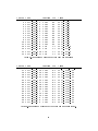
Number
16
17
18
19
20
21
22
23
24
25
26
27
28
29
30
31
Name
FPGA_PIN_P85
FPGA_PIN_P83
FPGA_PIN_P78
FPGA_PIN_P71
FPGA_PIN_P68
FPGA_PIN_P66
FPGA_PIN_P63
FPGA_PIN_P61
FPGA_PIN_P58
FPGA_PIN_P54
FPGA_PIN_P41
FPGA_PIN_P36
FPGA_PIN_P34
FPGA_PIN_P32
FPGA_PIN_P25
FPGA_PIN_P22
Function
GPIO
GPIO
GPIO
GPIO
GPIO
GPIO
GPIO
GPIO
GPIO
GPIO
GPIO
GPIO
GPIO
GPIO
GPIO
GPIO
PPS
I/O
I/O
I/O
I/O
I/O
I/O
I/O
I/O
I/O
I/O
I/O
I/O
I/O
I/O
I/O
I/O
Alias
WING_B_0
WING_B_1
WING_B_2
WING_B_3
WING_B_4
WING_B_5
WING_B_6
WING_B_7
WING_B_8
WING_B_9
WING_B_10
WING_B_11
WING_B_12
WING_B_13
WING_B_14
WING_B_15
Table 6.4: GF Papilio One 250 pin mappings (cont.)
45
Number
32
33
34
35
36
37
38
39
40
41
42
43
44
45
46
47
Name
FPGA_PIN_P91
FPGA_PIN_P92
FPGA_PIN_P94
FPGA_PIN_P95
FPGA_PIN_P98
FPGA_PIN_P2
FPGA_PIN_P3
FPGA_PIN_P4
FPGA_PIN_P5
FPGA_PIN_P9
FPGA_PIN_P10
FPGA_PIN_P11
FPGA_PIN_P12
FPGA_PIN_P15
FPGA_PIN_P16
FPGA_PIN_P17
Function
GPIO
GPIO
GPIO
GPIO
GPIO
GPIO
GPIO
GPIO
GPIO
GPIO
GPIO
GPIO
GPIO
GPIO
GPIO
GPIO
PPS
I/O
I/O
I/O
I/O
I/O
I/O
I/O
I/O
I/O
I/O
I/O
I/O
I/O
I/O
I/O
I/O
Alias
WING_C_0
WING_C_1
WING_C_2
WING_C_3
WING_C_4
WING_C_5
WING_C_6
WING_C_7
WING_C_8
WING_C_9
WING_C_10
WING_C_11
WING_C_12
WING_C_13
WING_C_14
WING_C_15
Table 6.5: GF Papilio One 250 pin mappings (cont.)
Number Name
Function PPS Alias
48 FPGA_PIN_P24 GPO
N/A FPGA_PIN_FLASHCS
SPI_FLASH_SEL_PIN
Table 6.6: GF Papilio One 250 pin mappings (cont.)
IO Slot
0
1
2
3
4
5
6
7
8-15
Device
SPI
UART
GPIO
Timers
Interrupt
SigmaDelta
SPI
CRC16
Notes
Connected to SPI ash
Connected to FT2232
1×16 bit (one PWM), 1×24 bit (one PWM)
Hardcoded
Mapped to PPS
Mapped to PPS
empty
Table 6.7: GF Papilio One 250 IO slot usage
46
6.3 Gadget Factory Papilio One 500
FPGA:
Frequency:
Memory size:
Bootloader size:
Stack size:
SPI ash:
Reset type:
GPIO count:
UART:
SPI:
SigmaDelta
Timers:
PWM outputs:
SPI sketch oset:
Xilinx Spartan 3E 500, VQ100 (xc3s500e-4-vq100)
96MHz (from on-board 32MHz oscillator)
32KiB
4KiB
2KiB
Any supported
UART Serial reset
49
2 (one connected to FTDI2232, other PPS)
2 (one connected to SPI ash, other PPS)
1 2-channel 16-bit (PPS)
2 (one 16-bit, one 24-bit)
2
0x00046000
Table 6.8: Gadget Factory Papilio One 500
IO
I
I
O
O
O
O
O
O
O
Index
0
1
0
1
2
3
4
5
6
Mapping
USPI MISO
UART2 RX
SigmaDelta channel 0
Timer 0 PWM 0
Timer 1 PWM 0
USPI MOSI
USPI SCK
SigmaDelta channel 1
UART2 TX
Alias
IOPIN_USPI_MISO
none
IOPIN_SIGMADELTA0
IOPIN_TIMER0_OC
IOPIN_TIMER1_OC
IOPIN_USPI_MOSI
IOPIN_USPI_SCK
IOPIN_SIGMADELTA1
none
Table 6.9: GF Papilio One 500 PPS mappings
47
Number
0
1
2
3
4
5
6
7
8
9
10
11
12
13
14
15
Name
FPGA_PIN_P18
FPGA_PIN_P23
FPGA_PIN_P26
FPGA_PIN_P33
FPGA_PIN_P35
FPGA_PIN_P40
FPGA_PIN_P53
FPGA_PIN_P57
FPGA_PIN_P60
FPGA_PIN_P62
FPGA_PIN_P65
FPGA_PIN_P67
FPGA_PIN_P70
FPGA_PIN_P79
FPGA_PIN_P84
FPGA_PIN_P86
Function
GPIO
GPIO
GPIO
GPIO
GPIO
GPIO
GPIO
GPIO
GPIO
GPIO
GPIO
GPIO
GPIO
GPIO
GPIO
GPIO
PPS
I/O
I/O
I/O
I/O
I/O
I/O
I/O
I/O
I/O
I/O
I/O
I/O
I/O
I/O
I/O
I/O
Alias
WING_A_0
WING_A_1
WING_A_2
WING_A_3
WING_A_4
WING_A_5
WING_A_6
WING_A_7
WING_A_8
WING_A_9
WING_A_10
WING_A_11
WING_A_12
WING_A_13
WING_A_14
WING_A_15
Table 6.10: GF Papilio One 500 pin mappings
Number
16
17
18
19
20
21
22
23
24
25
26
27
28
29
30
31
Name
FPGA_PIN_P85
FPGA_PIN_P83
FPGA_PIN_P78
FPGA_PIN_P71
FPGA_PIN_P68
FPGA_PIN_P66
FPGA_PIN_P63
FPGA_PIN_P61
FPGA_PIN_P58
FPGA_PIN_P54
FPGA_PIN_P41
FPGA_PIN_P36
FPGA_PIN_P34
FPGA_PIN_P32
FPGA_PIN_P25
FPGA_PIN_P22
Function
GPIO
GPIO
GPIO
GPIO
GPIO
GPIO
GPIO
GPIO
GPIO
GPIO
GPIO
GPIO
GPIO
GPIO
GPIO
GPIO
PPS
I/O
I/O
I/O
I/O
I/O
I/O
I/O
I/O
I/O
I/O
I/O
I/O
I/O
I/O
I/O
I/O
Alias
WING_B_0
WING_B_1
WING_B_2
WING_B_3
WING_B_4
WING_B_5
WING_B_6
WING_B_7
WING_B_8
WING_B_9
WING_B_10
WING_B_11
WING_B_12
WING_B_13
WING_B_14
WING_B_15
Table 6.11: GF Papilio One 500 pin mappings (cont.)
48
Number
32
33
34
35
36
37
38
39
40
41
42
43
44
45
46
47
Name
FPGA_PIN_P91
FPGA_PIN_P92
FPGA_PIN_P94
FPGA_PIN_P95
FPGA_PIN_P98
FPGA_PIN_P2
FPGA_PIN_P3
FPGA_PIN_P4
FPGA_PIN_P5
FPGA_PIN_P9
FPGA_PIN_P10
FPGA_PIN_P11
FPGA_PIN_P12
FPGA_PIN_P15
FPGA_PIN_P16
FPGA_PIN_P17
Function
GPIO
GPIO
GPIO
GPIO
GPIO
GPIO
GPIO
GPIO
GPIO
GPIO
GPIO
GPIO
GPIO
GPIO
GPIO
GPIO
PPS
I/O
I/O
I/O
I/O
I/O
I/O
I/O
I/O
I/O
I/O
I/O
I/O
I/O
I/O
I/O
I/O
Alias
WING_C_0
WING_C_1
WING_C_2
WING_C_3
WING_C_4
WING_C_5
WING_C_6
WING_C_7
WING_C_8
WING_C_9
WING_C_10
WING_C_11
WING_C_12
WING_C_13
WING_C_14
WING_C_15
Table 6.12: GF Papilio One 500 pin mappings (cont.)
Number Name
Function Alias
48 FPGA_PIN_P24 GPO
N/A FPGA_PIN_FLASHCS
SPI_FLASH_SEL_PIN
Table 6.13: GF Papilio One 500 pin mappings (cont.)
49
IO Slot
0
1
2
3
4
5
6
7
8-10
11
12-15
Device
SPI
UART
GPIO
Timers
Interrupt
SigmaDelta
SPI
CRC16
empty
UART
Notes
Connected to SPI ash
Connected to FT2232
1×16 bit (one PWM), 1×24 bit (one PWM)
Hardcoded
Mapped to PPS
Mapped to PPS
Mapped to PPS
empty
Table 6.14: GF Papilio One 500 IO slot usage
50
6.4 Spartan3E Starter Kit (S3E500)
FPGA:
Frequency:
Memory size:
Bootloader size:
Stack size:
SPI ash:
Reset type:
GPIO count:
UART:
SPI:
SigmaDelta
Timers:
PWM outputs:
SPI sketch oset:
Xilinx Spartan 3E 500, FG320 (xc3s500e-4-fg320)
96MHz (from on-board 50MHz oscillator)
32KiB
4KiB
2KiB
Any supported (usually M25P16)
UART Serial reset and reset (SOUTH) button
54
1 (connected to RS232 interface)
2 (one connected to board SPI bus, other PPS)
1 2-channel 16-bit (PPS)
2 (one 16-bit, one 24-bit)
2
0x00000000
Table 6.15: Spartan3E Starter Kit (S3E500)
IO
I
O
O
O
O
O
O
Index
0
0
1
2
3
4
5
Mapping
USPI MISO
SigmaDelta channel 0
Timer 0 PWM 0
Timer 1 PWM 0
USPI MOSI
USPI SCK
SigmaDelta channel 1
Alias
IOPIN_USPI_MISO
IOPIN_SIGMADELTA0
IOPIN_TIMER0_OC
IOPIN_TIMER1_OC
IOPIN_USPI_MOSI
IOPIN_USPI_SCK
IOPIN_SIGMADELTA1
Table 6.16: Spartan3E Starter Kit (S3E500) PPS mappings
51
Number
0
1
2
3
4
5
6
7
8
9
10
11
12
13
14
15
Name
FPGA_PIN_B4
FPGA_PIN_A4
FPGA_PIN_D5
FPGA_PIN_C5
FPGA_PIN_A6
FPGA_PIN_B6
FPGA_PIN_E7
FPGA_PIN_F7
FPGA_PIN_D7
FPGA_PIN_C7
FPGA_PIN_F8
FPGA_PIN_E8
FPGA_PIN_L13
FPGA_PIN_L14
FPGA_PIN_H18
FPGA_PIN_N17
Function
GPIO
GPIO
GPIO
GPIO
GPIO
GPIO
GPIO
GPIO
GPIO
GPIO
GPIO
GPIO
GPI
GPI
GPI
GPI
PPS
I/O
I/O
I/O
I/O
I/O
I/O
I/O
I/O
I/O
I/O
I/O
I/O
N/A
N/A
N/A
N/A
Alias
FPGA_J1_0
FPGA_J1_1
FPGA_J1_2
FPGA_J1_3
FPGA_J2_0
FPGA_J2_1
FPGA_J2_2
FPGA_J2_3
FPGA_J4_0
FPGA_J4_1
FPGA_J4_2
FPGA_J4_3
FPGA_SW_0
FPGA_SW_1
FPGA_SW_2
FPGA_SW_3
Table 6.17: Spartan3E Starter Kit (S3E500) pin mappings
Number
16
17
18
19
20
21
22
23
24
25
26
27
28
29
30
31
Name
FPGA_PIN_U3
FPGA_PIN_A13
FPGA_PIN_B13
FPGA_PIN_A14
FPGA_PIN_B14
FPGA_PIN_C14
FPGA_PIN_D14
FPGA_PIN_A16
FPGA_PIN_B16
FPGA_PIN_E13
FPGA_PIN_C4
FPGA_PIN_B11
FPGA_PIN_A11
FPGA_PIN_A8
FPGA_PIN_G9
FPGA_PIN_C3
Function
GPO
GPIO
GPIO
GPIO
GPIO
GPIO
GPIO
GPIO
GPIO
GPIO
GPIO
GPIO
GPIO
GPIO
GPIO
GPIO
PPS
N/A
I/O
I/O
I/O
I/O
I/O
I/O
I/O
I/O
I/O
I/O
I/O
I/O
I/O
I/O
I/O
Alias
SPI_FLASH_SEL_PIN
FPGA_FXIO_21
FPGA_FXIO_22
FPGA_FXIO_23
FPGA_FXIO_24
FPGA_FXIO_25
FPGA_FXIO_26
FPGA_FXIO_27
FPGA_FXIO_28
FPGA_FXIO_29
FPGA_FXIO_30
FPGA_FXIO_31
FPGA_FXIO_32
FPGA_FXIO_33
FPGA_FXIO_34
FPGA_FXIO_35
Table 6.18: Spartan3E Starter Kit (S3E500) pin mappings (cont.)
52
Number
32
33
34
35
36
37
38
39
40
41
42
43
44
45
46
47
Name
FPGA_PIN_F12
FPGA_PIN_E12
FPGA_PIN_E11
FPGA_PIN_F11
FPGA_PIN_C11
FPGA_PIN_D11
FPGA_PIN_E9
FPGA_PIN_F9
FPGA_PIN_R15
FPGA_PIN_R16
FPGA_PIN_P17
FPGA_PIN_M15
FPGA_PIN_L18
FPGA_PIN_L17
FPGA_PIN_M18
FPGA_PIN_P7
Function
GPO
GPO
GPO
GPO
GPO
GPO
GPO
GPO
GPIO
GPIO
GPIO
GPIO
GPO
GPO
GPO
GPO
PPS
N/A
N/A
N/A
N/A
N/A
N/A
N/A
N/A
N/A
N/A
N/A
N/A
N/A
N/A
N/A
N/A
Alias
FPGA_LED_0
FPGA_LED_1
FPGA_LED_2
FPGA_LED_3
FPGA_LED_4
FPGA_LED_5
FPGA_LED_6
FPGA_LED_7
FPGA_LCD_D4
FPGA_LCD_D5
FPGA_LCD_D6
FPGA_LCD_D7
FPGA_LCD_RS
FPGA_LCD_RW
FPGA_LCD_E
FPGA_AMP_SHDN
Table 6.19: Spartan3E Starter Kit (S3E500) pin mappings (cont.)
Number
48
49
50
51
52
53
Name
FPGA_PIN_K18
FPGA_PIN_G18
FPGA_PIN_V16
FPGA_PIN_P11
FPGA_PIN_N8
FPGA_PIN_N7
Function
GPO
GPO
GPO
GPO
GPO
GPO
PPS
N/A
N/A
N/A
N/A
N/A
N/A
Alias
FPGA_ROT_A
FPGA_ROT_B
FPGA_ROT_C
FPGA_AD_CONV
FPGA_DAC_CS
FPGA_AMP_CS
Table 6.20: Spartan3E Starter Kit (S3E500) pin mappings (cont.)
53
IO Slot
0
1
2
3
4
5
6
7
8-15
Device
SPI
UART
GPIO
Timers
Interrupt
SigmaDelta
SPI
CRC16
Notes
Connected to board SPI bus
Connected to RS232
1×16 bit (one PWM), 1×24 bit (one PWM)
Hardcoded
Mapped to PPS
Mapped to PPS
empty
Table 6.21: Spartan3E Starter Kit (S3E500) IO slot usage
54
7 Legal information
7.1 Licensing
See individual parts for licensing information. Most HDL code is released under BSD
license, some parts using GNU GPL license.
The Arduino IDE (and its modications) are licensed under GPLv2 license.
The ZPU toolchain components (binutils, gcc and gdb) have their own licensing information.
This document and the web site are released under Creative Commons Attribution
Share-Alike (cc by-sa).
7.2 Disclaimer
THIS DESIGN IS PROVIDED BY THE COPYRIGHT HOLDERS AND CONTRIBUTORS "AS IS" AND ANY EXPRESS OR IMPLIED WARRANTIES, INCLUDING,
BUT NOT LIMITED TO, THE IMPLIED WARRANTIES OF MERCHANTABILITY AND FITNESS FOR A PARTICULAR PURPOSE ARE DISCLAIMED. IN NO
EVENT SHALL THE COPYRIGHT HOLDER OR CONTRIBUTORS BE LIABLE
FOR ANY DIRECT, INDIRECT, INCIDENTAL, SPECIAL, EXEMPLARY, OR CONSEQUENTIAL DAMAGES (INCLUDING, BUT NOT LIMITED TO, PROCUREMENT OF SUBSTITUTE GOODS OR SERVICES; LOSS OF USE, DATA, OR PROFITS; OR BUSINESS INTERRUPTION) HOWEVER CAUSED AND ON ANY THEORY OF LIABILITY, WHETHER IN CONTRACT, STRICT LIABILITY, OR TORT
(INCLUDING NEGLIGENCE OR OTHERWISE) ARISING IN ANY WAY OUT OF
THE USE OF THIS PROJECT, EVEN IF ADVISED OF THE POSSIBILITY OF
SUCH DAMAGE.
55


![2008 [DAMN SMALL NAS]](http://vs1.manualzilla.com/store/data/005757702_2-ad0d2f1082977ee9ed587e807bbc0127-150x150.png)