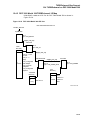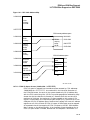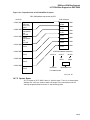
1
OpenVMS AXP Device Support:
Developer’s Guide
Order Number: AA–Q28SA–TE
March 1994
This manual describes how to write an OpenVMS AXP device driver and,
once it is written, how to compile, link, and load it into the OpenVMS
AXP operating system.
Revision/Update Information:
This is a new manual.
Software Version:
OpenVMS AXP Version 6.1
Digital Equipment Corporation
Maynard, Massachusetts
March 1994
Digital Equipment Corporation makes no representations that the use of its products in the
manner described in this publication will not infringe on existing or future patent rights, nor do
the descriptions contained in this publication imply the granting of licenses to make, use, or sell
equipment or software in accordance with the description.
Possession, use, or copying of the software described in this publication is authorized only pursuant
to a valid written license from Digital or an authorized sublicensor.
© Digital Equipment Corporation 1994. All rights reserved.
The postpaid Reader’s Comments forms at the end of this document request your critical evaluation
to assist in preparing future documentation.
The following are trademarks of Digital Equipment Corporation: Alpha AXP, AXP, Bookreader,
DECnet, DECwindows, Digital, MASSBUS, MSCP, OpenVMS, Q22–bus, TMSCP, TURBOchannel,
UNIBUS, VAX, VAXBI, VAX DOCUMENT, VAXcluster, VAX MACRO, VMS, VMScluster, and the
DIGITAL logo.
The following are third-party trademarks:
Futurebus/Plus is a registered trademark of Force Computers GMBH, Federal Republic of Germany.
Intel is a third-party trademark of Intel Corporation.
All other trademarks and registered trademarks are the property of their respective holders.
ZK6322
This document is available on CD–ROM.
This document was prepared using VAX DOCUMENT Version 2.1.
Send Us Your Comments
We welcome your comments on this or any other OpenVMS manual. If you have suggestions for
improving a particular section or find any errors, please indicate the title, order number, chapter,
section, and page number (if available). We also welcome more general comments. Your input is
valuable in improving future releases of our documentation.
You can send comments to us in the following ways:
[email protected]
•
Internet electronic mail:
•
Fax:
•
A completed Reader’s Comments form (postage paid, if mailed in the United States), or a
letter, via the postal service. Two Reader’s Comments forms are located at the back of each
printed OpenVMS manual. Please send letters and forms to:
603-881-0120 Attn: OpenVMS Documentation, ZKO3-4/U08
Digital Equipment Corporation
Information Design and Consulting
OpenVMS Documentation
110 Spit Brook Road, ZKO3-4/U08
Nashua, NH 03062-2698
USA
You may also use an online questionnaire to give us feedback. Print or edit the online file
SYS$HELP:OPENVMSDOC_SURVEY.TXT. Send the completed online file by electronic mail to our
Internet address, or send the completed hardcopy survey by fax or through the postal service.
Thank you.
Contents
Preface . . . . . . . . . . . . . . . . . . . . . . . . . . . . . . . . . . . . . . . . . . . . . . . . . . . . . . . . . . . .
xiii
1 Introduction
1.1
1.2
1.2.1
1.2.2
1.3
1.3.1
1.3.2
1.3.3
1.4
1.5
1.5.1
1.6
1.6.1
1.6.2
1.7
Driver Functions . . . . . . . . . . . . . . . . . . . . . . . . . . . . .
Driver Components . . . . . . . . . . . . . . . . . . . . . . . . . . .
Driver Tables . . . . . . . . . . . . . . . . . . . . . . . . . . . . .
Driver Routines . . . . . . . . . . . . . . . . . . . . . . . . . . .
I/O Database . . . . . . . . . . . . . . . . . . . . . . . . . . . . . . . .
Driver Tables . . . . . . . . . . . . . . . . . . . . . . . . . . . . .
Data Structures . . . . . . . . . . . . . . . . . . . . . . . . . . .
I/O Request Packets . . . . . . . . . . . . . . . . . . . . . . . .
Synchronization of Driver Activity . . . . . . . . . . . . . . . .
Driver Context . . . . . . . . . . . . . . . . . . . . . . . . . . . . . . .
Example of Driver Context-Switching . . . . . . . . . .
Programmed-I/O and Direct-Memory-Access Transfers
Programmed I/O . . . . . . . . . . . . . . . . . . . . . . . . . . .
Direct-Memory-Access I/O . . . . . . . . . . . . . . . . . . .
Buffered and Direct I/O . . . . . . . . . . . . . . . . . . . . . . . .
.
.
.
.
.
.
.
.
.
.
.
.
.
.
.
.
.
.
.
.
.
.
.
.
.
.
.
.
.
.
.
.
.
.
.
.
.
.
.
.
.
.
.
.
.
.
.
.
.
.
.
.
.
.
.
.
.
.
.
.
.
.
.
.
.
.
.
.
.
.
.
.
.
.
.
.
.
.
.
.
.
.
.
.
.
.
.
.
.
.
.
.
.
.
.
.
.
.
.
.
.
.
.
.
.
.
.
.
.
.
.
.
.
.
.
.
.
.
.
.
.
.
.
.
.
.
.
.
.
.
.
.
.
.
.
.
.
.
.
.
.
.
.
.
.
.
.
.
.
.
.
.
.
.
.
.
.
.
.
.
.
.
.
.
.
.
.
.
.
.
.
.
.
.
.
.
.
.
.
.
.
.
.
.
.
.
.
.
.
.
.
.
.
.
.
.
.
.
.
.
.
.
.
.
.
.
.
.
.
.
.
.
.
.
.
.
.
.
.
.
.
.
.
.
.
1–1
1–2
1–2
1–3
1–4
1–4
1–4
1–6
1–6
1–6
1–7
1–8
1–9
1–9
1–9
Mapping I/O Device Registers . . . . . . . . . . . . . . . . . . . . . . . . . .
Platform Independent I/O Bus Mapping . . . . . . . . . . . . . . . . . .
Using the IOC$MAP_IO Routine . . . . . . . . . . . . . . . . . . . . .
Platform Independent I/O Access Routines . . . . . . . . . . . . .
Accessing Registers Directly . . . . . . . . . . . . . . . . . . . . . . . . . . .
Accessing Registers Using CRAMS . . . . . . . . . . . . . . . . . . . . . .
Allocating CRAMs . . . . . . . . . . . . . . . . . . . . . . . . . . . . . . . . . . .
Preallocating CRAMs to a Device Unit or Device Controller
Calling IOC$ALLOCATE_CRAM to Obtain a CRAM . . . . . .
Constructing a Mailbox Command Within a CRAM . . . . . . . . . .
Register Data Byte Lane Alignment . . . . . . . . . . . . . . . . . .
Initiating a Mailbox Transaction . . . . . . . . . . . . . . . . . . . . . . . .
.
.
.
.
.
.
.
.
.
.
.
.
.
.
.
.
.
.
.
.
.
.
.
.
.
.
.
.
.
.
.
.
.
.
.
.
.
.
.
.
.
.
.
.
.
.
.
.
.
.
.
.
.
.
.
.
.
.
.
.
.
.
.
.
.
.
.
.
.
.
.
.
.
.
.
.
.
.
.
.
.
.
.
.
.
.
.
.
.
.
.
.
.
.
.
.
2–2
2–2
2–3
2–3
2–4
2–4
2–4
2–5
2–5
2–6
2–7
2–7
.
.
.
.
.
.
.
.
.
.
.
.
.
.
.
.
.
.
.
.
.
.
.
.
.
.
.
.
.
.
.
.
.
.
.
.
.
.
.
.
3–2
3–3
3–5
3–6
3–6
2 Accessing Device Interface Registers
2.1
2.2
2.2.1
2.2.2
2.3
2.4
2.5
2.5.1
2.5.2
2.6
2.6.1
2.7
3 Allocating Map Registers and Other Counted Resources
3.1
3.2
3.3
3.4
3.5
Allocating a Counted Resource Context Block . .
Allocating Counted Resource Items . . . . . . . . . .
Loading Map Registers . . . . . . . . . . . . . . . . . . .
Deallocating a Number of Counted Resources . .
Deallocating a Counted Resource Context Block
.
.
.
.
.
.
.
.
.
.
.
.
.
.
.
.
.
.
.
.
.
.
.
.
.
.
.
.
.
.
.
.
.
.
.
.
.
.
.
.
.
.
.
.
.
.
.
.
.
.
.
.
.
.
.
.
.
.
.
.
v
4 Writing Device-Driver Tables
4.1
4.2
4.3
4.3.1
4.3.1.1
4.4
4.4.1
4.4.1.1
4.4.1.2
4.4.2
4.4.2.1
4.4.2.2
4.4.2.3
4.4.3
4.4.3.1
4.4.3.2
4.4.4
4.4.4.1
Driver Prologue Table . . . . . . . . . . . . . . . . . . . . . .
Driver Dispatch Table . . . . . . . . . . . . . . . . . . . . . .
Function Decision Table . . . . . . . . . . . . . . . . . . . . .
OpenVMS AXP I/O Function Codes . . . . . . . . .
Defining Device-Specific Function Codes . .
Building Driver Tables Using C . . . . . . . . . . . . . . .
Driver Prologue Table . . . . . . . . . . . . . . . . . . .
DPT Macros . . . . . . . . . . . . . . . . . . . . . . . .
DPT Functions . . . . . . . . . . . . . . . . . . . . . .
Driver Dispatch Table . . . . . . . . . . . . . . . . . . .
DDT Fields . . . . . . . . . . . . . . . . . . . . . . . . .
DDT Functions . . . . . . . . . . . . . . . . . . . . . .
DDT Macro Calls . . . . . . . . . . . . . . . . . . . .
Function Decision Table . . . . . . . . . . . . . . . . . .
FDT Functions . . . . . . . . . . . . . . . . . . . . . .
FDT Macros . . . . . . . . . . . . . . . . . . . . . . . .
Device Database Initialization/Reinitialization
DPT_STORE_ISR . . . . . . . . . . . . . . . . . . . .
.
.
.
.
.
.
.
.
.
.
.
.
.
.
.
.
.
.
.
.
.
.
.
.
.
.
.
.
.
.
.
.
.
.
.
.
.
.
.
.
.
.
.
.
.
.
.
.
.
.
.
.
.
.
.
.
.
.
.
.
.
.
.
.
.
.
.
.
.
.
.
.
.
.
.
.
.
.
.
.
.
.
.
.
.
.
.
.
.
.
.
.
.
.
.
.
.
.
.
.
.
.
.
.
.
.
.
.
.
.
.
.
.
.
.
.
.
.
.
.
.
.
.
.
.
.
.
.
.
.
.
.
.
.
.
.
.
.
.
.
.
.
.
.
.
.
.
.
.
.
.
.
.
.
.
.
.
.
.
.
.
.
.
.
.
.
.
.
.
.
.
.
.
.
.
.
.
.
.
.
.
.
.
.
.
.
.
.
.
.
.
.
.
.
.
.
.
.
.
.
.
.
.
.
.
.
.
.
.
.
.
.
.
.
.
.
.
.
.
.
.
.
.
.
.
.
.
.
.
.
.
.
.
.
.
.
.
.
.
.
.
.
.
.
.
.
.
.
.
.
.
.
.
.
.
.
.
.
.
.
.
.
.
.
.
.
.
.
.
.
.
.
.
.
.
.
.
.
.
.
.
.
.
.
.
.
.
.
.
.
.
.
.
.
.
.
.
.
.
.
.
.
.
.
.
.
.
.
.
.
.
.
.
.
.
.
.
.
.
.
.
.
.
.
4–1
4–3
4–4
4–6
4–9
4–9
4–10
4–10
4–11
4–11
4–11
4–12
4–13
4–13
4–14
4–14
4–14
4–14
.
.
.
.
.
.
.
.
.
.
.
.
.
.
.
.
.
.
.
.
.
.
.
.
.
.
.
.
.
.
.
.
.
.
.
.
.
.
.
.
.
.
.
.
.
.
.
.
.
.
.
.
.
.
.
.
.
.
.
.
.
.
.
.
.
.
.
.
.
.
.
.
.
.
.
.
.
.
.
.
.
.
.
.
.
.
.
.
.
.
.
.
.
.
.
.
.
.
.
.
.
.
.
.
.
.
.
.
.
.
.
.
.
.
.
.
.
.
.
.
.
.
.
.
.
.
.
.
.
.
.
.
.
.
.
.
.
.
.
.
.
.
.
.
.
.
.
.
.
.
.
.
.
.
.
.
.
.
.
.
.
.
5–2
5–2
5–3
5–5
5–7
5–7
5–8
5–8
5–8
Transferring Control to the Start-I/O Routine . . . . . . . . . . . . . . . . . . . .
Context of a Driver Fork Process . . . . . . . . . . . . . . . . . . . . . . . . . . . . . .
Functions of a Start-I/O Routine . . . . . . . . . . . . . . . . . . . . . . . . . . . . . .
Obtaining Controller Access . . . . . . . . . . . . . . . . . . . . . . . . . . . . . . .
Obtaining and Converting the I/O Function Code and Its Modifiers .
Preparing the Device Activation Bit Mask . . . . . . . . . . . . . . . . . . . .
Synchronizing Access to the Device Database . . . . . . . . . . . . . . . . .
Checking for a Local Processor Power Failure . . . . . . . . . . . . . . . . .
Activating the Device . . . . . . . . . . . . . . . . . . . . . . . . . . . . . . . . . . . .
Waiting for an Interrupt or Timeout . . . . . . . . . . . . . . . . . . . . . . . . . . .
.
.
.
.
.
.
.
.
.
.
.
.
.
.
.
.
.
.
.
6–1
6–1
6–2
6–2
6–3
6–3
6–3
6–3
6–4
6–4
Servicing a Solicited Interrupt . . . . . . . . . . . . . . . . . . . . . . . . . . . . . . . . . .
Servicing an Unsolicited Interrupt . . . . . . . . . . . . . . . . . . . . . . . . . . . . . . .
7–1
7–3
5 Writing FDT Routines
5.1
5.2
5.2.1
5.2.2
5.3
5.4
5.4.1
5.4.2
5.4.3
Context of Driver FDT Processing . . . . . . . . . . .
Upper-Level FDT Action Routines . . . . . . . . . . .
System-Provided Upper-Level FDT Routines
FDT Exit Paths . . . . . . . . . . . . . . . . . . . . . .
FDT Routines for System Direct I/O . . . . . . . . .
FDT Routines for System Buffered I/O . . . . . . .
Checking Accessibility of the User’s Buffer .
Allocating the System Buffer . . . . . . . . . . . .
Buffered-I/O Postprocessing . . . . . . . . . . . . .
.
.
.
.
.
.
.
.
.
.
.
.
.
.
.
.
.
.
6 Writing a Start-I/O Routine
6.1
6.2
6.3
6.3.1
6.3.2
6.3.3
6.3.4
6.3.5
6.3.6
6.4
7 Writing an Interrupt Service Routine
7.1
7.2
vi
8 Completing an I/O Request and Handling Timeouts
8.1
I/O Postprocessing . . . . . . . . . . . . . . . . . . . . . . . . . . . . . . . . .
8.1.1
EXE_STD$PRIMITIVE_FORK . . . . . . . . . . . . . . . . . . . . .
8.1.2
Completing an I/O Request . . . . . . . . . . . . . . . . . . . . . . .
8.1.2.1
Releasing the Controller . . . . . . . . . . . . . . . . . . . . . .
8.1.2.2
Saving Status, Count, and Device-Dependent Status .
8.1.2.3
Returning Control to the Operating System . . . . . . . .
8.2
Timeout Handling Routines . . . . . . . . . . . . . . . . . . . . . . . . . .
8.2.1
Retrying an I/O Operation . . . . . . . . . . . . . . . . . . . . . . . .
8.2.2
Aborting an I/O Request . . . . . . . . . . . . . . . . . . . . . . . . .
8.2.3
Sending a Message to the Operator . . . . . . . . . . . . . . . . .
.
.
.
.
.
.
.
.
.
.
.
.
.
.
.
.
.
.
.
.
.
.
.
.
.
.
.
.
.
.
.
.
.
.
.
.
.
.
.
.
.
.
.
.
.
.
.
.
.
.
.
.
.
.
.
.
.
.
.
.
.
.
.
.
.
.
.
.
.
.
.
.
.
.
.
.
.
.
.
.
.
.
.
.
.
.
.
.
.
.
.
.
.
.
.
.
.
.
.
.
8–1
8–1
8–2
8–2
8–2
8–3
8–3
8–5
8–5
8–6
Linker Options File for OpenVMS AXP Device Drivers . . . . . . . . . . . . . . .
Resolving CRTL References at Link-Time . . . . . . . . . . . . . . . . . . . . . . . . .
9–2
9–4
9 Linking a Device Driver
9.1
9.2
10 Loading an OpenVMS AXP Device Driver
10.1
Manually Connecting Devices and Loading Drivers . . . . . . . . . . . . . . . . . .
10.1.1
Obtaining the Adapter’s TR Number . . . . . . . . . . . . . . . . . . . . . . . . . .
10.1.2
Obtaining the Adapter’s CSR Address . . . . . . . . . . . . . . . . . . . . . . . . .
10.1.3
Locating the Adapter’s Interrupt Vectors . . . . . . . . . . . . . . . . . . . . . . .
10.2
I/O Configuration Support in SYSMAN . . . . . . . . . . . . . . . . . . . . . . . . . . .
AUTOCONFIGURE . . . . . . . . . . . . . . . . . . . . . . . . . . . . . . . . . . . . . . . . . .
CONNECT . . . . . . . . . . . . . . . . . . . . . . . . . . . . . . . . . . . . . . . . . . . . . . . . .
SET PREFIX . . . . . . . . . . . . . . . . . . . . . . . . . . . . . . . . . . . . . . . . . . . . . . .
SHOW BUS . . . . . . . . . . . . . . . . . . . . . . . . . . . . . . . . . . . . . . . . . . . . . . . .
SHOW DEVICE . . . . . . . . . . . . . . . . . . . . . . . . . . . . . . . . . . . . . . . . . . . . .
SHOW PREFIX . . . . . . . . . . . . . . . . . . . . . . . . . . . . . . . . . . . . . . . . . . . . .
10.3
Loading Sliced Executive Images . . . . . . . . . . . . . . . . . . . . . . . . . . . . . . . .
10.3.1
Controlling Executive Image Slicing . . . . . . . . . . . . . . . . . . . . . . . . . .
10.3.1.1
XDELTA Support for Executive Image Slicing . . . . . . . . . . . . . . . .
10.3.1.2
Locating Source Modules with Image Slicing Enabled . . . . . . . . . .
10–1
10–1
10–2
10–2
10–3
10–4
10–5
10–8
10–9
10–10
10–12
10–13
10–14
10–14
10–14
11 Debugging a Device Driver
11.1
Using the Delta/XDelta Debugger . . . . . . . . . . . . . . . . . . . . . . . . . . . . . . .
11.2
Using the OpenVMS AXP System-Code Debugger . . . . . . . . . . . . . . . . . . .
11.2.1
User-interface Options . . . . . . . . . . . . . . . . . . . . . . . . . . . . . . . . . . . . .
11.2.2
Building a System Image to Be Debugged . . . . . . . . . . . . . . . . . . . . . .
11.2.3
Setting Up the Target System for Connections . . . . . . . . . . . . . . . . . .
11.2.3.1
Making Connections Between the Target Kernel and the
System-Code Debugger . . . . . . . . . . . . . . . . . . . . . . . . . . . . . . . . .
11.2.3.2
Interactions between XDELTA and the Target Kernel/System-Code
Debugger . . . . . . . . . . . . . . . . . . . . . . . . . . . . . . . . . . . . . . . . . . . .
11.2.4
Setting Up the Host System . . . . . . . . . . . . . . . . . . . . . . . . . . . . . . . . .
11.2.5
Starting the System-Code Debugger . . . . . . . . . . . . . . . . . . . . . . . . . .
11.2.6
Summary of OpenVMS Debugger Commands . . . . . . . . . . . . . . . . . . .
11.2.7
System-Code Debugger Network Information . . . . . . . . . . . . . . . . . . .
11.3
Troubleshooting Checklist . . . . . . . . . . . . . . . . . . . . . . . . . . . . . . . . . . . . .
11.4
Troubleshooting Network Failures . . . . . . . . . . . . . . . . . . . . . . . . . . . . . . .
11–1
11–2
11–2
11–3
11–3
11–6
11–6
11–7
11–8
11–8
11–11
11–11
11–11
vii
.
.
.
.
.
11–12
11–12
11–13
11–13
11–15
12.1
TURBOchannel Overview . . . . . . . . . . . . . . . . . . . . . . . . . . . . . . . . . . . . .
12.2
TURBOchannel on DEC 3000 Model 500 . . . . . . . . . . . . . . . . . . . . . . . . . .
12.2.1
DEC 3000 Model 500 TURBOchannel Address Map . . . . . . . . . . . . . .
12.2.2
Dense and Sparse Space Addressing . . . . . . . . . . . . . . . . . . . . . . . . . .
12.2.3
DEC 3000 Model 500 TURBOchannel Register Access . . . . . . . . . . . .
12.2.3.1
Direct Register Access on DEC 3000 Model 500
TURBOchannel . . . . . . . . . . . . . . . . . . . . . . . . . . . . . . . . . . . . . . .
12.2.3.2
Mailbox Register Access on DEC 3000 Model 500
TURBOchannel . . . . . . . . . . . . . . . . . . . . . . . . . . . . . . . . . . . . . . .
12.2.3.3
DEC 3000 Model 500 TURBOchannel DMA . . . . . . . . . . . . . . . . .
12.2.3.4
Physical DMA . . . . . . . . . . . . . . . . . . . . . . . . . . . . . . . . . . . . . . . .
12.2.3.5
Virtual DMA . . . . . . . . . . . . . . . . . . . . . . . . . . . . . . . . . . . . . . . . .
12.2.3.6
Scatter/Gather Map Management . . . . . . . . . . . . . . . . . . . . . . . . .
12.2.3.7
Allocating Scatter/Gather Map Entries . . . . . . . . . . . . . . . . . . . . .
12.2.3.8
Loading Scatter/Gather Map Entries . . . . . . . . . . . . . . . . . . . . . . .
12.2.4
DEC 3000 Model 500/TURBOchannel Interface Registers . . . . . . . . . .
12.2.4.1
IOSLOT Register . . . . . . . . . . . . . . . . . . . . . . . . . . . . . . . . . . . . . .
12.2.4.2
IMASK Register . . . . . . . . . . . . . . . . . . . . . . . . . . . . . . . . . . . . . . .
12.2.4.3
IOC$NODE_FUNCTION . . . . . . . . . . . . . . . . . . . . . . . . . . . . . . . .
12.2.4.4
DEC 3000 Model 500 TURBOchannel I/O Space Map . . . . . . . . . .
12.2.5
Configuring a Device on DEC 3000 Model 500/TURBOchannel . . . . . .
12.2.6
IOC$NODE_DATA . . . . . . . . . . . . . . . . . . . . . . . . . . . . . . . . . . . . . . . .
12.3
TURBOchannel on DEC 3000 Model 400 . . . . . . . . . . . . . . . . . . . . . . . . . .
12.4
TURBOchannel on DEC 3000 Model 300 . . . . . . . . . . . . . . . . . . . . . . . . . .
12.4.1
DEC 3000 Model 300/Turbochannal Address Map . . . . . . . . . . . . . . . .
12.4.2
TURBOchannel Interrupts on DEC 3000 Model 300 . . . . . . . . . . . . . .
12.4.3
IOC$NODE_FUNCTION on DEC 3000 Model 300 . . . . . . . . . . . . . . .
12.4.4
IOC$NODE_DATA on DEC 3000 Model 300 . . . . . . . . . . . . . . . . . . . .
12.4.5
DEC 3000 Model 300/TURBOchannel I/O Map . . . . . . . . . . . . . . . . . .
12–1
12–1
12–2
12–2
12–4
11.4.1
11.4.1.1
11.4.1.2
11.4.1.3
11.4.2
Access to Symbols in OpenVMS Executive Images . . . . . . . . . . . .
Overview of How the OpenVMS Debugger Maintains Symbols
Overview of OpenVMS Executive Image Symbols . . . . . . . . . .
Possible Problems You May Encounter . . . . . . . . . . . . . . . . . .
Sample System-Code Debugging Session . . . . . . . . . . . . . . . . . . . .
.
.
.
.
.
.
.
.
.
.
12 TURBOchannel Bus Support
12–4
12–6
12–9
12–9
12–9
12–10
12–10
12–11
12–11
12–12
12–12
12–13
12–13
12–15
12–15
12–16
12–17
12–18
12–18
12–18
12–18
12–19
13 PCI Bus Support
13.1
13.2
13.3
13.4
13.5
13.6
13.7
13.8
13.9
13.10
13.11
13.12
13.13
viii
PCI Addressing . . . . . . . . . . . . . . . . . . . . . . . . . . . . . . . . . . . .
PCI Configuration Space . . . . . . . . . . . . . . . . . . . . . . . . . . . . .
PCI as an I/O Bus on AXP Platforms . . . . . . . . . . . . . . . . . . . .
PCI Device Interrupts . . . . . . . . . . . . . . . . . . . . . . . . . . . . . . .
OpenVMS AXP PCI Bus Support Data Structures . . . . . . . . . .
Probing the PCI to Find Devices . . . . . . . . . . . . . . . . . . . . . . .
Register Access on PCI Buses . . . . . . . . . . . . . . . . . . . . . . . . .
Finding the PCI Physical Addresses Assigned to a Device . . . .
Mapping a PCI Physical Address . . . . . . . . . . . . . . . . . . . . . . .
PCI Configuration Space Base Address Register Format . . . . .
When to Call IOC$MAP_IO and Where to Keep IOHANDLES
Direct Memory Access (DMA) on the PCI Bus . . . . . . . . . . . . .
Configuring a PCI Device and Loading A Driver . . . . . . . . . . .
.
.
.
.
.
.
.
.
.
.
.
.
.
.
.
.
.
.
.
.
.
.
.
.
.
.
.
.
.
.
.
.
.
.
.
.
.
.
.
.
.
.
.
.
.
.
.
.
.
.
.
.
.
.
.
.
.
.
.
.
.
.
.
.
.
.
.
.
.
.
.
.
.
.
.
.
.
.
.
.
.
.
.
.
.
.
.
.
.
.
.
.
.
.
.
.
.
.
.
.
.
.
.
.
.
.
.
.
.
.
.
.
.
.
.
.
.
13–1
13–2
13–3
13–3
13–4
13–4
13–5
13–5
13–6
13–8
13–9
13–9
13–10
14 EISA and ISA Bus Support
14.1
Evolution of the EISA Bus . . . . . . . . . . . . . . . . . . . . . . . . . . . . . . . . . . . . .
14.2
Intel 82350DT EISA Chipset . . . . . . . . . . . . . . . . . . . . . . . . . . . . . . . . . . .
14.3
EISA Bus Resources . . . . . . . . . . . . . . . . . . . . . . . . . . . . . . . . . . . . . . . . . .
14.3.1
IRQs . . . . . . . . . . . . . . . . . . . . . . . . . . . . . . . . . . . . . . . . . . . . . . . . . . .
14.3.2
DMA Channel . . . . . . . . . . . . . . . . . . . . . . . . . . . . . . . . . . . . . . . . . . .
14.3.3
I/O Port Addresses . . . . . . . . . . . . . . . . . . . . . . . . . . . . . . . . . . . . . . . .
14.3.4
EISA Memory Addresses . . . . . . . . . . . . . . . . . . . . . . . . . . . . . . . . . . .
14.3.5
EISA Configuration Utility . . . . . . . . . . . . . . . . . . . . . . . . . . . . . . . . .
14.4
EISA Interrupts . . . . . . . . . . . . . . . . . . . . . . . . . . . . . . . . . . . . . . . . . . . . .
14.5
EISA DMA Support . . . . . . . . . . . . . . . . . . . . . . . . . . . . . . . . . . . . . . . . . .
14.6
EISA I/O Address Map . . . . . . . . . . . . . . . . . . . . . . . . . . . . . . . . . . . . . . . .
14.7
EISA Bus Support on DEC 2000 . . . . . . . . . . . . . . . . . . . . . . . . . . . . . . . .
14.7.1
DEC 2000 System Address Map . . . . . . . . . . . . . . . . . . . . . . . . . . . . .
14.7.1.1
DEC 2000 Address Space . . . . . . . . . . . . . . . . . . . . . . . . . . . . . . . .
14.7.1.2
DEC 2000 System Memory (0-FFF.FFFF) . . . . . . . . . . . . . . . . . . .
14.7.1.3
INTA Cycle Access (1.0000.0000) . . . . . . . . . . . . . . . . . . . . . . . . . .
14.7.1.4
NVRAM Access (1.8000.0000, 1.A000.0000) . . . . . . . . . . . . . . . . . .
14.7.1.5
VTI VL82C106 Combination Chip (1.C000.0000) . . . . . . . . . . . . . .
14.7.1.6
Host Address Extension Register (1.D000.0000) . . . . . . . . . . . . . .
14.7.1.7
System Control Register Access ( 1.E000.0000) . . . . . . . . . . . . . . .
14.7.1.8
EISA Memory Space Access (2.0000.0000 - 2.FFFF.FFFF) . . . . . . .
14.7.1.9
EISA I/O Space Access (3.0000.0000 - 3.FFFF.FFFF) . . . . . . . . . . .
14.7.2
Sparse Space . . . . . . . . . . . . . . . . . . . . . . . . . . . . . . . . . . . . . . . . . . . .
14.7.3
Register Access . . . . . . . . . . . . . . . . . . . . . . . . . . . . . . . . . . . . . . . . . .
14.7.3.1
Direct Register Access . . . . . . . . . . . . . . . . . . . . . . . . . . . . . . . . . .
14.7.3.2
CRAM Register Access . . . . . . . . . . . . . . . . . . . . . . . . . . . . . . . . . .
14.7.4
DMA on DEC 2000 . . . . . . . . . . . . . . . . . . . . . . . . . . . . . . . . . . . . . . .
14.7.4.1
DMA Example . . . . . . . . . . . . . . . . . . . . . . . . . . . . . . . . . . . . . . . .
14.7.5
I/O Interrupts on DEC 2000 . . . . . . . . . . . . . . . . . . . . . . . . . . . . . . . . .
14.7.5.1
EISA IRQs . . . . . . . . . . . . . . . . . . . . . . . . . . . . . . . . . . . . . . . . . . .
14.7.5.2
SCB Vectors . . . . . . . . . . . . . . . . . . . . . . . . . . . . . . . . . . . . . . . . . .
14.7.5.3
EOI . . . . . . . . . . . . . . . . . . . . . . . . . . . . . . . . . . . . . . . . . . . . . . . .
14.7.6
EISA Bus Interface Registers . . . . . . . . . . . . . . . . . . . . . . . . . . . . . . . .
14.7.6.1
Interrupt Enable Register . . . . . . . . . . . . . . . . . . . . . . . . . . . . . . .
14.7.6.2
End of Interrupt Command . . . . . . . . . . . . . . . . . . . . . . . . . . . . . .
14.7.6.3
IOC$NODE_FUNCTION and IOC$NODE_DATA . . . . . . . . . . . . .
14.7.6.3.1
IOC$NODE_FUNCTION . . . . . . . . . . . . . . . . . . . . . . . . . . . . .
14.7.6.3.2
IOC$NODE_DATA . . . . . . . . . . . . . . . . . . . . . . . . . . . . . . . . . .
14.7.6.3.3
CRB$L_NODE . . . . . . . . . . . . . . . . . . . . . . . . . . . . . . . . . . . . .
14.7.7
DEC 2000 I/O Space Map . . . . . . . . . . . . . . . . . . . . . . . . . . . . . . . . . .
14.7.8
Configuring a Device on DEC 2000 . . . . . . . . . . . . . . . . . . . . . . . . . . .
14.7.8.1
Vector parameter . . . . . . . . . . . . . . . . . . . . . . . . . . . . . . . . . . . . . .
14.7.8.2
Node parameter . . . . . . . . . . . . . . . . . . . . . . . . . . . . . . . . . . . . . . .
14.7.8.3
CSR parameter . . . . . . . . . . . . . . . . . . . . . . . . . . . . . . . . . . . . . . .
14.7.8.4
Resource Assignment on DEC 2000 . . . . . . . . . . . . . . . . . . . . . . . .
14.7.8.4.1
IRQ’s . . . . . . . . . . . . . . . . . . . . . . . . . . . . . . . . . . . . . . . . . . . .
14.7.8.4.2
EISA Memory Addresses . . . . . . . . . . . . . . . . . . . . . . . . . . . . .
14.7.8.4.3
ISA I/O Port Addresses . . . . . . . . . . . . . . . . . . . . . . . . . . . . . .
14–1
14–2
14–2
14–2
14–2
14–3
14–3
14–3
14–4
14–4
14–5
14–6
14–6
14–7
14–7
14–8
14–8
14–8
14–8
14–9
14–9
14–11
14–13
14–14
14–14
14–14
14–15
14–15
14–16
14–16
14–17
14–17
14–17
14–17
14–17
14–17
14–17
14–18
14–19
14–19
14–20
14–21
14–21
14–21
14–21
14–21
14–22
14–22
ix
15 Futurebus+ Bus Support
15.1
Futurebus+ Overview . . . . . . . . . . . . . . . . . . . . . . . . . . . . . . . . . . . . . . . . .
15.2
Futurebus+ Address Space . . . . . . . . . . . . . . . . . . . . . . . . . . . . . . . . . . . . .
15.3
Futurebus+ CSR Addressing . . . . . . . . . . . . . . . . . . . . . . . . . . . . . . . . . . .
15.4
CSR Data Format . . . . . . . . . . . . . . . . . . . . . . . . . . . . . . . . . . . . . . . . . . .
15.5
Futurebus+ Register Access . . . . . . . . . . . . . . . . . . . . . . . . . . . . . . . . . . . .
15.5.1
Allocating CRAMs for Futurebus+ Register Access . . . . . . . . . . . . . . .
15.5.2
Initializing CRAMS . . . . . . . . . . . . . . . . . . . . . . . . . . . . . . . . . . . . . . .
15.5.3
Issuing the Futurebus+ Register Access . . . . . . . . . . . . . . . . . . . . . . .
15.6
DMA . . . . . . . . . . . . . . . . . . . . . . . . . . . . . . . . . . . . . . . . . . . . . . . . . . . . .
15.7
Futurebus+ Interrupts . . . . . . . . . . . . . . . . . . . . . . . . . . . . . . . . . . . . . . . .
15.8
Futurebus+ System Routines . . . . . . . . . . . . . . . . . . . . . . . . . . . . . . . . . . .
15.8.1
IOC$RESERVE_FBUS_A32 . . . . . . . . . . . . . . . . . . . . . . . . . . . . . . . . .
15.8.2
IOC$RESERVE_FBUS_A64 . . . . . . . . . . . . . . . . . . . . . . . . . . . . . . . . .
15.9
Configuring a Futurebus+ Adapter . . . . . . . . . . . . . . . . . . . . . . . . . . . . . .
15.10 Futurebus+ Bus Probing During Booting . . . . . . . . . . . . . . . . . . . . . . . . . .
15.11 Futurebus+ on DEC 4000 . . . . . . . . . . . . . . . . . . . . . . . . . . . . . . . . . . . . .
15.11.1
The DEC 4000 Futurebus+ Bridge . . . . . . . . . . . . . . . . . . . . . . . . . . . .
15.11.2
DEC 4000 Futurebus+ Address Space . . . . . . . . . . . . . . . . . . . . . . . . .
15.11.3
DEC 4000 ADP List . . . . . . . . . . . . . . . . . . . . . . . . . . . . . . . . . . . . . . .
15.12 Futurebus+ on DEC 10000/7000 . . . . . . . . . . . . . . . . . . . . . . . . . . . . . . . .
15.12.1
The DEC 10000/7000 Futurebus+ Bridge . . . . . . . . . . . . . . . . . . . . . . .
15.12.2
DEC 10000/7000 Futurebus+ Address Space . . . . . . . . . . . . . . . . . . . .
15.12.3
DEC 10000/7000 ADP List . . . . . . . . . . . . . . . . . . . . . . . . . . . . . . . . . .
15–1
15–1
15–2
15–4
15–5
15–5
15–5
15–6
15–6
15–6
15–8
15–8
15–8
15–9
15–11
15–12
15–12
15–12
15–13
15–14
15–14
15–15
15–16
A Device Support Bus Routines
IOC$ALLOC_CNT_RES . . . .
IOC$ALLOC_CRAB . . . . . . .
IOC$ALLOC_CRCTX . . . . . .
IOC$ALLOCATE_CRAM . . .
IOC$CANCEL_CNT_RES . .
IOC$CRAM_CMD . . . . . . . .
IOC$CRAM_IO . . . . . . . . . .
IOC$CRAM_QUEUE . . . . . .
IOC$CRAM_WAIT . . . . . . . .
IOC$DEALLOC_CNT_RES .
IOC$DEALLOC_CRAB . . . .
IOC$DEALLOC_CRCTX . . .
IOC$DEALLOCATE_CRAM .
IOC$MAP_IO . . . . . . . . . . . .
IOC$READ_IO . . . . . . . . . . .
IOC$UNMAP_IO . . . . . . . . .
IOC$WRITE_IO . . . . . . . . . .
x
.
.
.
.
.
.
.
.
.
.
.
.
.
.
.
.
.
.
.
.
.
.
.
.
.
.
.
.
.
.
.
.
.
.
.
.
.
.
.
.
.
.
.
.
.
.
.
.
.
.
.
.
.
.
.
.
.
.
.
.
.
.
.
.
.
.
.
.
.
.
.
.
.
.
.
.
.
.
.
.
.
.
.
.
.
.
.
.
.
.
.
.
.
.
.
.
.
.
.
.
.
.
.
.
.
.
.
.
.
.
.
.
.
.
.
.
.
.
.
.
.
.
.
.
.
.
.
.
.
.
.
.
.
.
.
.
.
.
.
.
.
.
.
.
.
.
.
.
.
.
.
.
.
.
.
.
.
.
.
.
.
.
.
.
.
.
.
.
.
.
.
.
.
.
.
.
.
.
.
.
.
.
.
.
.
.
.
.
.
.
.
.
.
.
.
.
.
.
.
.
.
.
.
.
.
.
.
.
.
.
.
.
.
.
.
.
.
.
.
.
.
.
.
.
.
.
.
.
.
.
.
.
.
.
.
.
.
.
.
.
.
.
.
.
.
.
.
.
.
.
.
.
.
.
.
.
.
.
.
.
.
.
.
.
.
.
.
.
.
.
.
.
.
.
.
.
.
.
.
.
.
.
.
.
.
.
.
.
.
.
.
.
.
.
.
.
.
.
.
.
.
.
.
.
.
.
.
.
.
.
.
.
.
.
.
.
.
.
.
.
.
.
.
.
.
.
.
.
.
.
.
.
.
.
.
.
.
.
.
.
.
.
.
.
.
.
.
.
.
.
.
.
.
.
.
.
.
.
.
.
.
.
.
.
.
.
.
.
.
.
.
.
.
.
.
.
.
.
.
.
.
.
.
.
.
.
.
.
.
.
.
.
.
.
.
.
.
.
.
.
.
.
.
.
.
.
.
.
.
.
.
.
.
.
.
.
.
.
.
.
.
.
.
.
.
.
.
.
.
.
.
.
.
.
.
.
.
.
.
.
.
.
.
.
.
.
.
.
.
.
.
.
.
.
.
.
.
.
.
.
.
.
.
.
.
.
.
.
.
.
.
.
.
.
.
.
.
.
.
.
.
.
.
.
.
.
.
.
.
.
.
.
.
.
.
.
.
.
.
.
.
.
.
.
.
.
.
.
.
.
.
.
.
.
.
.
.
.
.
.
.
.
.
.
.
.
.
.
.
.
.
.
.
.
.
.
.
.
.
.
.
.
.
.
.
.
.
.
.
.
.
.
.
.
.
.
.
.
.
.
.
.
.
.
.
.
.
.
.
.
.
.
.
.
.
.
.
.
.
.
.
.
.
.
.
.
.
.
.
.
.
.
.
.
.
A–2
A–6
A–8
A–10
A–12
A–14
A–17
A–19
A–21
A–23
A–25
A–26
A–27
A–28
A–30
A–32
A–33
B Sample Driver Written in C
B.1
B.2
LRDRIVER Example . . . . . . . . . . . . . . . . . . . . . . . . . . . . . . . . . . . . . . . . .
LRDRIVER.COM . . . . . . . . . . . . . . . . . . . . . . . . . . . . . . . . . . . . . . . . . . . .
B–1
B–23
Linker Options File (xxDRIVER_LNK.OPT) for an OpenVMS AXP
Device Driver . . . . . . . . . . . . . . . . . . . . . . . . . . . . . . . . . . . . . . . . . .
Invoking the System-Code Debugger . . . . . . . . . . . . . . . . . . . . . . . .
Connecting to the Target System . . . . . . . . . . . . . . . . . . . . . . . . . . .
Target System Connection Display . . . . . . . . . . . . . . . . . . . . . . . . . .
Setting a Breakpoint . . . . . . . . . . . . . . . . . . . . . . . . . . . . . . . . . . . .
Finding the Source Code . . . . . . . . . . . . . . . . . . . . . . . . . . . . . . . . .
Using the Set Mode Screen Command . . . . . . . . . . . . . . . . . . . . . . .
Using the SCROLL/UP DEBUG Command . . . . . . . . . . . . . . . . . . .
Break Point Display . . . . . . . . . . . . . . . . . . . . . . . . . . . . . . . . . . . . .
Using the Debug Step Command . . . . . . . . . . . . . . . . . . . . . . . . . . .
Using the Examine and Show Calls Commands . . . . . . . . . . . . . . .
Canceling the Breakpoints . . . . . . . . . . . . . . . . . . . . . . . . . . . . . . . .
Using the Step Command . . . . . . . . . . . . . . . . . . . . . . . . . . . . . . . .
Using the Step/Return Command . . . . . . . . . . . . . . . . . . . . . . . . . .
Source Lines Error Message . . . . . . . . . . . . . . . . . . . . . . . . . . . . . .
Using the Show Image Command . . . . . . . . . . . . . . . . . . . . . . . . . .
.
.
.
.
.
.
.
.
.
.
.
.
.
.
.
.
.
.
.
.
.
.
.
.
.
.
.
.
.
.
.
.
9–3
11–15
11–16
11–16
11–16
11–18
11–18
11–19
11–20
11–21
11–22
11–23
11–24
11–25
11–26
11–27
I/O Database . . . . . . . . . . . . . . . . . . . . . . . . . . . . . . . . . . .
Layout of Function Decision Table (FDT) . . . . . . . . . . . . . .
Format of System Buffer for a Buffered-I/O Read Function
Traditional and Sliced Loads . . . . . . . . . . . . . . . . . . . . . . .
XDELTA Display . . . . . . . . . . . . . . . . . . . . . . . . . . . . . . . .
Option Register Layout . . . . . . . . . . . . . . . . . . . . . . . . . . .
Option Register Layout—Dense Space . . . . . . . . . . . . . . . .
Option Register Layout—Sparse Space . . . . . . . . . . . . . . .
Option Register Layout—Dense Space . . . . . . . . . . . . . . . .
Option Register Layout—Sparse Space . . . . . . . . . . . . . . .
Option Register Layout . . . . . . . . . . . . . . . . . . . . . . . . . . .
Option Register Layout—Sparse Space . . . . . . . . . . . . . . .
Scatter/Gather Map Entry . . . . . . . . . . . . . . . . . . . . . . . . .
TURBOchannel DMA Address . . . . . . . . . . . . . . . . . . . . . .
IOSLOT Register . . . . . . . . . . . . . . . . . . . . . . . . . . . . . . . .
IMASK . . . . . . . . . . . . . . . . . . . . . . . . . . . . . . . . . . . . . . . .
DEC 3000 Model 500 ADP List . . . . . . . . . . . . . . . . . . . . .
DEC 3000 Model 400 ADP List . . . . . . . . . . . . . . . . . . . . .
DEC 3000 Model 300 ADP List . . . . . . . . . . . . . . . . . . . . .
.
.
.
.
.
.
.
.
.
.
.
.
.
.
.
.
.
.
.
.
.
.
.
.
.
.
.
.
.
.
.
.
.
.
.
.
.
.
1–5
4–4
5–9
10–13
10–15
12–3
12–3
12–3
12–4
12–5
12–7
12–7
12–9
12–10
12–12
12–12
12–14
12–17
12–19
Index
Examples
9–1
11–1
11–2
11–3
11–4
11–5
11–6
11–7
11–8
11–9
11–10
11–11
11–12
11–13
11–14
11–15
Figures
1–1
4–1
5–1
10–1
10–2
12–1
12–2
12–3
12–4
12–5
12–6
12–7
12–8
12–9
12–10
12–11
12–12
12–13
12–14
.
.
.
.
.
.
.
.
.
.
.
.
.
.
.
.
.
.
.
.
.
.
.
.
.
.
.
.
.
.
.
.
.
.
.
.
.
.
.
.
.
.
.
.
.
.
.
.
.
.
.
.
.
.
.
.
.
.
.
.
.
.
.
.
.
.
.
.
.
.
.
.
.
.
.
.
.
.
.
.
.
.
.
.
.
.
.
.
.
.
.
.
.
.
.
.
.
.
.
.
.
.
.
.
.
.
.
.
.
.
.
.
.
.
.
.
.
.
.
.
.
.
.
.
.
.
.
.
.
.
.
.
.
xi
14–1
14–2
14–3
14–4
14–5
15–1
15–2
15–3
15–4
15–5
15–6
15–7
15–8
15–9
15–10
15–11
15–12
DEC 2000 Address Map . . . . . . . . . . . . . . . . .
EISA Memory Address Space . . . . . . . . . . . . .
DEC 2000 Address Map . . . . . . . . . . . . . . . . .
Expanded view of DEC 2000/EISA I/O Space .
DEC 2000 ADP List . . . . . . . . . . . . . . . . . . . .
32 Bit Futurebus+ Address Space . . . . . . . . .
Format of an A32 CSR Address . . . . . . . . . . .
Big-Endian Register Data Format . . . . . . . . .
Little Endian Register Data Format . . . . . . .
Futurebus+ Target Register . . . . . . . . . . . . . .
System Control Block . . . . . . . . . . . . . . . . . . .
System Control Block . . . . . . . . . . . . . . . . . . .
DEC 4000 Futurebus+ Address Space . . . . . .
DEC 4000 ADP list . . . . . . . . . . . . . . . . . . . .
Futurebus+ A32 Space . . . . . . . . . . . . . . . . . .
Futurebus+ A64 Space . . . . . . . . . . . . . . . . . .
DEC 10000/7000 ADP List . . . . . . . . . . . . . . .
.
.
.
.
.
.
.
.
.
.
.
.
.
.
.
.
.
.
.
.
.
.
.
.
.
.
.
.
.
.
.
.
.
.
.
.
.
.
.
.
.
.
.
.
.
.
.
.
.
.
.
.
.
.
.
.
.
.
.
.
.
.
.
.
.
.
.
.
.
.
.
.
.
.
.
.
.
.
.
.
.
.
.
.
.
.
.
.
.
.
.
.
.
.
.
.
.
.
.
.
.
.
.
.
.
.
.
.
.
.
.
.
.
.
.
.
.
.
.
.
.
.
.
.
.
.
.
.
.
.
.
.
.
.
.
.
.
.
.
.
.
.
.
.
.
.
.
.
.
.
.
.
.
.
.
.
.
.
.
.
.
.
.
.
.
.
.
.
.
.
.
.
.
.
.
.
.
.
.
.
.
.
.
.
.
.
.
.
.
.
.
.
.
.
.
.
.
.
.
.
.
.
.
.
.
.
.
.
.
.
.
.
.
.
.
.
.
.
.
.
.
.
.
.
.
.
.
.
.
.
.
.
.
.
.
.
.
.
.
.
.
.
.
.
.
.
.
.
.
.
.
.
.
.
.
.
.
.
.
.
.
.
.
.
.
.
.
.
.
.
.
.
.
.
.
.
.
.
.
.
.
.
.
.
.
.
.
.
.
.
.
.
.
.
.
.
.
.
.
.
.
.
.
.
.
.
.
.
.
.
.
.
.
.
.
.
.
.
.
.
.
.
.
14–7
14–10
14–11
14–13
14–20
15–2
15–3
15–4
15–4
15–7
15–10
15–11
15–13
15–14
15–15
15–16
15–17
OpenVMS Macros and System Routines That Manage I/O Mailbox
Operations . . . . . . . . . . . . . . . . . . . . . . . . . . . . . . . . . . . . . . . . . . . .
Mailbox Command Indices Defined by cramdef.h . . . . . . . . . . . . . . .
I/O Function Codes . . . . . . . . . . . . . . . . . . . . . . . . . . . . . . . . . . . . .
DPT Initialization Macros for C . . . . . . . . . . . . . . . . . . . . . . . . . . . .
System-Provided Upper-Level FDT Action Routines . . . . . . . . . . . .
FDT Completion Macros and Associated Routines . . . . . . . . . . . . . .
SELECT Qualifier Examples . . . . . . . . . . . . . . . . . . . . . . . . . . . . . .
.
.
.
.
.
.
.
.
.
.
.
.
.
.
2–4
2–6
4–6
4–10
5–3
5–5
10–4
Tables
2–1
2–2
4–1
4–2
5–1
5–2
10–1
xii
Preface
Intended Audience
This manual is intended for system programmers who want to write an OpenVMS
AXP device driver. A future edition of this book will describe how to write an
OpenVMS AXP device driver in a high-level language.
Associated Documents
The OpenVMS AXP Device Support: Reference contains more detailed information
about the routines and macros mentioned in this book.
Conventions
In this manual, every use of OpenVMS AXP means the OpenVMS AXP operating
system.
The following conventions are also used in this manual:
Ctrl/x
A sequence such as Ctrl/x indicates that you must hold down
the key labeled Ctrl while you press another key or a pointing
device button.
PF1 x
A sequence such as PF1 x indicates that you must first press
and release the key labeled PF1 and then press and release
another key or a pointing device button.
Return
In examples, a key name enclosed in a box indicates that
you press a key on the keyboard. (In text, a key name is not
enclosed in a box.)
...
Horizontal ellipsis points in examples indicate one of the
following possibilities:
•
Additional optional arguments in a statement have been
omitted.
•
The preceding item or items can be repeated one or more
times.
•
Additional parameters, values, or other information can be
entered.
.
.
.
Vertical ellipsis points indicate the omission of items from
a code example or command format; the items are omitted
because they are not important to the topic being discussed.
()
In command format descriptions, parentheses indicate that, if
you choose more than one option, you must enclose the choices
in parentheses.
xiii
[]
In command format descriptions, brackets indicate optional
elements. You can choose one, none, or all of the options.
(Brackets are not optional, however, in the syntax of a directory
name in an OpenVMS file specification or in the syntax of a
substring specification in an assignment statement.)
{}
In command format descriptions, braces surround a required
choice of options; you must choose one of the options listed.
boldface text
Boldface text represents the introduction of a new term or the
name of an argument, an attribute, or a reason (user action
that triggers a callback).
Boldface text is also used to show user input in Bookreader
versions of the manual.
xiv
italic text
Italic text emphasizes important information and indicates
complete titles of manuals and variables. Variables include
information that varies in system messages (Internal error
number), in command lines (/PRODUCER=name), and in
command parameters in text (where device-name contains up
to five alphanumeric characters).
UPPERCASE TEXT
Uppercase text indicates a command, the name of a routine,
the name of a file, or the abbreviation for a system privilege.
struct
Monospace type in text identifies the following C programming
language elements: keywords, the names of independently
compiled external functions and files, syntax summaries, and
references to variables or identifiers introduced in an example.
-
A hyphen in code examples indicates that additional
arguments to the request are provided on the line that follows.
numbers
All numbers in text are assumed to be decimal unless
otherwise noted. Nondecimal radixes—binary, octal, or
hexadecimal—are explicitly indicated.
1
Introduction
An OpenVMS device driver is a set of routines and tables that the operating
system uses to process an I/O request for a particular device such as disks, tapes,
and network controllers.
The operating system’s approach to I/O is that the system should perform as
much of the processing of an I/O request as possible and that drivers should limit
themselves to the device-specific aspects of I/O processing. To accomplish this,
the operating system provides drivers with the following services:
•
A Queue I/O request ($QIO) system service that preprocesses an I/O request
by performing those functions and checks that are common to all devices; for
example, validating those arguments of the I/O request that are not device
specific
•
Many operating system routines that drivers can call to perform I/O
preprocessing, allocate and deallocate resources, and synchronize driver
execution
•
A system I/O postprocessing routine that performs device-independent I/O
postprocessing for all I/O requests
Thus, drivers can leave the device-independent I/O processing to the operating
system and can concentrate on servicing those aspects of an I/O operation that
vary from device type to device type. In addition, drivers can call system routines
to perform many functions that are common to several, but not all, devices.
A device driver does not run sequentially from beginning to end. Rather, the
operating system uses driver tables and other information maintained by itself
and the driver to determine which driver routines to activate and when they
should be activated. Because little sequential processing of driver code occurs,
the operating system must assume the responsibility for synchronizing the
execution of the various driver routines, as well as the execution of all drivers in
the system.
This chapter defines the general functions and purposes of a device driver. It
then introduces concepts crucial to an understanding of how device drivers work
within the operating system and integral to the process of successfully writing
one. It concludes with a brief description of the flow of driver activity in servicing
an I/O request.
1.1 Driver Functions
A system utility loads a device driver into system virtual address space and
creates its associated data structures. Once loaded, a device driver controls I/O
operations on a peripheral device by performing the following functions:
•
Defining the peripheral device for the rest of the operating system
1–1
Introduction
1.1 Driver Functions
•
Preparing a device unit and its controller (or both) for operation at system
startup and during recovery from a power failure
•
Performing device-dependent I/O preprocessing
•
Translating programmed requests for I/O operations into device-specific
commands
•
Activating a device unit
•
Responding to hardware interrupts generated by a device unit
•
Responding to device timeout conditions
•
Responding to requests to cancel I/O on a device unit
•
Reporting device errors to an error-logging program
•
Returning status from a device unit to the process that requested the I/O
operation
1.2 Driver Components
A device driver module can consist of the routines and tables discussed in this
section. The order of the routines and tables within the driver module is not
important.
1.2.1 Driver Tables
The following tables appear in every driver.
The driver prologue table (DPT) defines the identity and attributes or
characteristics of the driver to the system utility that loads the driver into
virtual memory and creates the associated data structures. With the information
provided in the DPT, the driver-loading procedure can both load and reload
drivers and perform the I/O database initialization that is appropriate to either
situation.
Section 4.1 describes the procedure for creating a DPT and further discusses its
functions. The DPT contents are shown and described in the OpenVMS AXP
Device Support: Reference.
The driver dispatch table (DDT) lists the addresses of the entry points of
standard routines within the driver, and records the size of the diagnostic
and error message buffers for drivers that perform error logging. You can find
additional information and instructions on how to specify a DDT in Section 4.2.
The structure and contents of the DDT are shown and described in the OpenVMS
AXP Device Support: Reference.
The function decision table (FDT) lists all valid function codes for the device,
and associates valid codes with the addresses of I/O preprocessing routines, called
FDT routines. The driver contains device-dependent FDT routines, and the
operating system itself provides routines (described in Section 5.2.1) that perform
request preprocessing common to many I/O functions.
When a user process calls the $QIO system service, the system service uses the
I/O function code specified in the request to select the appropriate upperlevel
FDT routine. To prepare for the actual I/O operation, FDT routines perform
such tasks as allocating buffers in system space, locking pages in memory, and
validating the device-dependent arguments (p1 to p6) of the $QIO request.
Section 4.3 provides further discussion of the FDT, and Chapter 5 details
strategies and rules for writing, specifying, and exiting from an FDT routine.
1–2
Introduction
1.2 Driver Components
1.2.2 Driver Routines
In addition to any FDT routines it might contain, a device driver generally
contains both a start-I/O routine and an interrupt service routine (ISR).
The start-I/O routine performs such additional device-dependent tasks as
translating the I/O function code into a device-specific command, storing the
details of the user request in the device’s unit control block (UCB) in the I/O
database and, if necessary, obtaining access to controller and adapter resources.
Whenever the start-I/O routine must wait for these resources to become available,
the operating system suspends the routine, reactivating it when the resources
become free.
The start-I/O routine ultimately activates the device by suitably loading the
device’s registers. At this stage, the start-I/O routine invokes a system macro
that causes its execution to be suspended until the device completes the I/O
operation and posts an interrupt to the processor. The start-I/O routine remains
suspended until the driver’s interrupt service routine handles the interrupt.
When a device posts an interrupt, its driver’s interrupt service routine determines
whether the interrupt is expected or unexpected, and takes appropriate action.
If the interrupt is expected, the interrupt service routine reactivates the driver’s
start-I/O routine at the point of suspension. The general course of action of driver
mainline code at this time is to perform device-dependent I/O postprocessing
and to transfer control to the operating system for device-independent I/O
postprocessing.
Details on writing a start-I/O routine appear in Chapter 6. A description of a
driver interrupt service routine appears in Chapter 7.
You can also include any of the following routines in a device driver:
The unit initialization routine and controller initialization routine prepare
a device or controller for operation when the driver-loading procedure loads
the driver into memory and when the system recovers from a power failure. The
amount and type of initialization needed by devices and controllers vary according
to the device type and the I/O bus to which the device or controller is attached.
additional information about device driver initialization routines.
A timeout handling routine retries I/O operations and performs other error
handling when a device fails to complete a request in a reasonable period of time.
Once every second, the system timer checks all devices in the system for device
timeout. When it locates a device that has timed out, because it is off line or
some error has occurred, the system timer calls the driver’s timeout handling
routine.
Depending upon the reason for the timeout, the timeout handling routine may
call a system error-logging routine to allocate and fill an error message buffer
with information about the error. In turn, the error-logging routine can call a
register-dumping routine in the driver that also loads into the buffer the
contents of device registers at the time of the error.
The operating system calls a driver’s cancel-I/O routine when a user process
issues a Cancel I/O on Channel ($CANCEL) system service for the device. It may
also call the routine when the device’s reference count goes to zero, which occurs
when all users with assigned channels to the device have deassigned them.
1–3
Introduction
1.3 I/O Database
1.3 I/O Database
Because a driver and the operating system cooperate to process an I/O request,
they must have a common and current source of information about the request.
This is the function of the I/O database. The I/O database consists of the
following three parts:
•
Driver tables that allow the system to load drivers, to validate device
functions, and to call driver routines at their entry points
•
Data structures that describe I/O bus adapters, device types, device units,
device controllers, and logical paths from processes to devices
•
I/O request packets that define individual requests for I/O activity
Illustrations of I/O database structures and detailed descriptions of their fields
appear in the data structure chapter of the OpenVMS AXP Device Support:
Reference. Figure 1–1 illustrates some of the relationships among system I/O
routines, the I/O database, and a device driver.
1.3.1 Driver Tables
The three driver tables—driver prologue table, driver dispatch table, and function
decision table—are defined in every driver. Section 1.2 lists these tables and the
other components of a device driver, and Chapter 4 discusses their contents.
1.3.2 Data Structures
I/O database data structures describe peripheral hardware and are used by the
operating system to synchronize access to devices. The operating system creates
these data structures either at system startup or when a driver is loaded into the
system.
The system defines a unit control block (UCB) for each device unit attached to
the system. A UCB defines the characteristics and current state of an individual
device unit.
UCBs are the focal point of the I/O database. When a driver is suspended or
interrupted, the UCB keeps the context of the driver in a set of fields collectively
known as a fork block.1 In addition, the UCB contains the listhead for the
queue of pending I/O request packets (IRPs) for the unit.
A device data block (DDB) contains information common to all devices of the
same type that are connected to a particular controller. It records the generic
device name concatenated with the controller designator (for example, LPA,
DKB), and the name and location of the associated device driver. In addition,
the DDB contains a pointer to the first UCB for the device units attached to the
controller.
The operating system creates a channel request block (CRB) for each
controller. A CRB defines the current state of the controller and lists the
devices waiting for the controller’s data channel. It also contains a pointer to the
interrupt service routine (ISR).
1
1–4
Other structures, such as the CRB, also include a fork block. The discussion of fork
blocks and fork processes in Section 1.5 explains the role of fork blocks in driver
processing.
Introduction
1.3 I/O Database
Figure 1–1 I/O Database
Process
Control
Block
( describes
requesting
process)
I/O
Request
Packet
(describes
I/O
request)
DDB
(for device
type)
DDT
(locates
driver)
UCB
(describes
device)
Driver
FDT Routine
Driver
Start I/O Routine
Driver
Interrupt Service
Routine
CRB
(synchronizes
controller)
Driver
Controller Initialization
Routine
CCB
(describes
logical path
to device)
IDB
(describes
controller)
ADP
(describes
adapter)
Device
registers
ZK−1766−GE
The system also creates for each controller an interrupt dispatch block (IDB).
An IDB lists the device units associated with a controller and points to the UCB
of the device unit that the controller is currently servicing. In addition, an IDB
points to device registers and the controller’s I/O adapter.
An adapter control block (ADP) defines the characteristics and current state
of an I/O adapter such as the TURBOchannel interface on a DEC 3000. An
ADP contains the information necessary to allocate the adapter’s resources. The
operating system provides routines that drivers can call to interface with the
appropriate adapter.
The channel control block (CCB) describes the logical path between a process
and the UCB of a specific device unit.2 Each process owns a number of CCBs.
2
Channel request blocks (CRBs) and channel control blocks (CCBs) are two separate data
structures. To help distinguish the two, it may be helpful to think of the channel request
block as the ‘‘controller request’’ block because it describes the hardware controller. In
contrast, the channel control block is used by a process and a device unit to manage the
1–5
Introduction
1.3 I/O Database
When a process issues the Assign I/O Channel ($ASSIGN) system service, the
system writes a description of the assigned device to the CCB.
Unlike the data structures mentioned earlier, a CCB is not located in nonpaged
system space, but in the process’s control region (P1 space).
1.3.3 I/O Request Packets
The third part of the I/O database is a set of I/O request packets. When a process
requests I/O activity, the operating system constructs an I/O request packet
(IRP), that describes the I/O request in a standard form.
The IRP contains fields into which the system and driver I/O preprocessing
routines can write information: for instance, the device-dependent arguments
specified in the call to the $QIO system service. The packet also includes buffer
addresses, a pointer to the target device’s UCB, an I/O function code, and
pointers to the I/O database. After preprocessing, the IRP can be queued to a list
originating in the device’s UCB to await processing by the driver.
When the device unit is free and the IRP is next in line to be processed on the
unit, the system sends it to the device driver’s start-I/O routine. The start-I/O
routine uses the IRP as its source of detailed instructions about the operation to
be performed.
1.4 Synchronization of Driver Activity
Device drivers and other kernel-mode code must maintain synchronization with
other priority operating system activities. The term synchronization refers to
the means by which such code accesses shared data in a consistent, orderly, and
predictable fashion. Because there may be more than one processor active in an
OpenVMS AXP system, system-level code must synchronize its actions with other
code threads it may have preempted on the same (or local) processor, as well as
with those that are active (or to be activated) on other processors in the system.
The operating system uses hardware and software interrupt priority levels (IPLs)
to order system events on each local processor in an OpenVMS AXP system.
AXP hardware defines 32 interrupt priority levels (IPLs). The higher numbered
IPLs (16 to 31) are reserved for hardware interrupts, such as those posted by
devices. The operating system uses the lower numbered IPLs (0 to 15). Code that
executes at a higher IPL takes precedence over code that executes at a lower IPL.
A driver, in concert with the operating system, ensures that it maintains system
synchronization by performing certain activities and by accessing certain data
only at the appropriate IPL. In a multiprocessing system, the driver extends
the synchronization it achieves by executing locally at a given IPL by acquiring
ownership of the spinlock associated with the operation it is performing.
1.5 Driver Context
As indicated in Section 1.2.2, a driver may have several routines to which
the operating system may pass control in certain situations. The context in
which any one routine receives control from the operating system may differ
substantially from that in which another receives control. It is essential that a
driver routine not attempt to exceed the limitations of the context in which it
executes.
logical channel (the channel argument to the $ASSIGN and $QIO system services) in
accomplishing I/O operations.
1–6
Introduction
1.5 Driver Context
In general, context is characterized by the following factors:
•
Actual parameters that are passed to the routine
•
The current IPL of the executing processor
•
The range of IPLs that the routine can change and the required IPL on return
from the routine.
•
The currently owned spinlocks of the executing processor
•
The data structures available to the routine
•
The ability or inability to access process space
A complete description of the context of each driver routine appears in the entry
points chapter of the OpenVMS AXP Device Support: Reference. The following
are some general observations:
•
All device driver routines execute in kernel mode at an elevated IPL.
•
Only driver FDT routines execute within process context and can access
process space (P0 and P1).
•
The majority of driver routines execute in interrupt (or system context):
that is, in the sequence of execution that follows a processor’s grant of an
interrupt request at a given IPL. Such code can refer only to system (S0)
space. Moreover, it cannot incur exceptions, including page faults, without
causing a fatal bugcheck.
Most driver processing of an I/O request (before and after the device acknowledges
the servicing of the request by requesting an interrupt from the processor) occurs
at a fork IPL. This portion of driver code, which includes most of the start-I/O
routine, is commonly known as the driver’s fork process.
There are several instances in the processing of an I/O request when a driver
fork process must suspend execution to wait for a resource or a device interrupt.
To make the matter of saving and restoring fork process context as efficient as
possible, the operating system places a restriction on the context of a driver fork
process, in addition to those that apply to any process in interrupt context. Fork
context consists of the following:
•
The fork routine parameters (FR3 and FR4)
•
The fork routine address (FPC)
•
A fork block (usually the unit control block that can contain additional fork
process context
The operating system places the fork block of a suspended fork process in either
a processor-specific fork queue or a resource wait queue where it waits to be
resumed. When it resumes the fork process, the operating system calls the
fork routine with the FR3 value, FR4 value, and a pointer to the fork block as
parameters.
1.5.1 Example of Driver Context-Switching
Because a device driver consists of a number of routines that are activated by
the system, the operating system determines the context in which the routines
execute.
1–7
Introduction
1.5 Driver Context
As an example, consider the following write request that occurs without error:
1. A user process executing in user mode calls the $QIO system service to write
data to a device.
2. The $QIO system service gains control in process context but in kernel mode.
It performs device-independent preprocessing of the I/O request.
3. The system service uses the driver’s function decision table (FDT) to call the
appropriate FDT routines to perform device-dependent preprocessing. These
FDT routines execute in full process context in kernel mode.
4. When preprocessing is complete, a system routine creates a fork process to
execute the driver’s start-I/O routine in kernel mode.
5. The start-I/O routine activates the device unit and suspends itself. At this
point, the operating system suspends the fork process executing the start-I/O
routine and saves sufficient context to reactivate the start-I/O routine at the
point of suspension.
6. When the device completes the data transfer, it requests an interrupt. The
interrupt causes the system to activate the driver’s interrupt service routine.
7. The interrupt service routine executes to handle the device interrupt. It then
causes the start-I/O routine to resume in interrupt context.
8. The start-I/O routine regains control in interrupt context but almost
immediately issues a request to the operating system to transform its
context to that of a fork process. This action dismisses the interrupt.
9. When reactivated in fork process context, the start-I/O routine performs
device-specific I/O completion and passes control to the system for additional
I/O postprocessing.
10. System I/O postprocessing runs in interrupt context at a lower IPL and issues
a special kernel-mode asynchronous system trap (AST) for the user process
requesting I/O.
11. When the special kernel-mode AST is delivered, the AST routine executes in
full process context in kernel mode to deliver data and status to the process.
If the original request specified a user-mode AST, the special kernel-mode
AST queues it.
12. When the user process gains control, the user’s AST routine executes in full
process context in user mode.
1.6 Programmed-I/O and Direct-Memory-Access Transfers
Devices are equipped with various registers that initiate, control, and monitor
the progress of data transfer, seek operation, or other requests for device activity.
When it completes a request, the device posts an interrupt to the processor. The
size of the transfer concluded by a device interrupt depends upon the capabilities
of the device.
1–8
Introduction
1.6 Programmed-I/O and Direct-Memory-Access Transfers
1.6.1 Programmed I/O
Drivers for relatively slow devices, such as printers, terminals, and some disk and
tape drives, must transfer data to a hardware interface register a byte or a word
at a time. These drivers must themselves keep a record of the location of the data
buffer in memory, as well as a running count of the amount of data that has been
transferred to or from the device. Thus, these devices perform programmed I/O
(PIO) in that the transfer is largely conducted by the driver program.
The DE422 ISA ethernet interface is an example of a device that uses
programmed I/O.
Drivers performing PIO transfers are generally not concerned with the operation
of I/O adapters. However, drivers that perform direct-memory-access (DMA)
transfers must consider I/O adapter functions, as discussed in Section 1.6.2.
1.6.2 Direct-Memory-Access I/O
Devices that perform direct-memory-access (DMA) transfers do not require
the central processor so frequently. Once the driver activates the device, the
device can transfer a large amount of data without requesting an interrupt after
each of the smaller amounts. The responsibilities of a driver for a DMA device
involve setting a hardware interface register with the starting address of the
buffer containing the data to be transferred, a byte offset into the buffer, and
the size of the transfer. By setting the appropriate bit or bits in the hardware
interface control and status register (CSR), the driver activates the device. The
device then automatically transfers the specified amount of data to or from the
specified address. Any driver that does DMA must map the DMA buffer. For
DMA transfers, drivers must first map the transfer from main memory to I/O
bus memory space. The result of this mapping is a set of contiguous addresses in
the bus address space that the DMA device can access to successfully perform a
DMA transfer. If the bus interface does not have map registers, a bus address is
equivalent to a main memory address. If the bus interface has map registers, a
bus address undergoes a translation before becomming a system memory address.
1.7 Buffered and Direct I/O
A separate issue, but one related to the data transfer capabilities of a device,
results from the fact that the original buffer, as specified in the user $QIO
request, is in process space and is mapped by process page-table entries. Because
the driver cannot rely on process context existing at the time the device is ready
to service the I/O request, it must have some means of guaranteeing that it can
access both the data involved in the transfer and the page-table entries that map
the buffer.
The operating system provides the following two techniques that are employed by
device drivers:
•
Direct I/O, the technique used most commonly by drivers of DMA devices,
locks the user buffer in memory as well as the page-table entries that map
it. The function decision table (FDT) of such a driver calls a system-supplied
FDT routine that prepares the user buffer for direct I/O.
•
Buffered I/O is the strategy whereby the driver FDT dispatches to an FDT
routine in the driver that allocates a buffer from nonpaged pool. It is this
intermediate buffer that is involved in the transfer. The driver later refers
to the buffer using addresses in system space. Driver preprocessing routines
copy the data from the user buffer to the system buffer for a write request;
system I/O postprocessing (by means of a special kernel-mode AST) delivers
1–9
Introduction
1.7 Buffered and Direct I/O
data from the system buffer to the user buffer for a read request. Drivers
most often use buffered I/O for PIO devices such as line printers and card
readers.
The trade-off between buffered I/O and direct I/O is the time required to move the
data into the user’s buffer as against the time required to lock the buffer pages in
memory.
1–10
2
Accessing Device Interface Registers
A hardware interface register is the place where software interfaces with a
hardware component. Every hardware component on an OpenVMS AXP system,
including CPU and memory, has a set of interface registers.
The portion of a processor’s physical address space through which it accesses
hardware interface registers is known as its I/O space.
In the VAX architecture, a hardware implementation usually defines a physical
address boundary between memory space and I/O space. I/O space physical
addresses are mapped into the processors’ virtual address space and are accessed
using VAX load and store instructions (for example, MOV, BIS, and others).
For AXP systems, there are no rules governing how hardware implementations
allow access to I/O space. Some AXP platforms allow VAX-style I/O space access.
Other platforms provide access to I/O space through hardware I/O mailboxes.
Some platforms implement both styles of I/O register access.
The challenge presented by the AXP architecture is to create software
abstractions that hide the hardware mechanisms for I/O space access from the
programmer. These software abstractions contribute to driver portability. The
AXP architecture also defines no byte or word length load and store instructions.
Because some I/O buses and adapters require byte or word register access
granularity for correct adapter operation, AXP system hardware designers
invented the following mechanisms that provide byte and word access granularity
for I/O adapter register access:
•
Sparse space addressing, which means the device address space is
expanded by a factor of two to allow for inclusion of a byte mask in the write
data.
•
Swizzle space addressing, which means where upper order bits in the
processor physical address map to an I/O bus address, while lower order
bits are used to implement I/O bus byte enable signals. This causes a large
amount of processor physical address space to represent the I/O bus address
space.
•
Hardware I/O mailboxes, which are 64-byte, naturally-aligned, physicallycontiguous data structures (defined by the AXP architecture) built in system
memory and accessed by special I/O subsystem hardware. Drivers can use
hardware I/O mailboxes to deliver commands and write data to the interface
registers of a device residing on an I/O bus.
A significant part of I/O bus support in the OpenVMS AXP operating system is
to provide standard ways to access I/O device registers. OpenVMS AXP provides
a set of data structures and routines that can be used for register access on any
system, regardless of the underlying I/O hardware. Bus support provides two
ways. One way is the CRAM data structure. The other way is the platform
independent access routines IOC$READ_IO and IOC$WRITE_IO.
2–1
Accessing Device Interface Registers
Note
In register access discussions, the term control and status register
(CSR) is sometimes used instead of the generic term interface register.
In this manual, the terms are equivalent.
2.1 Mapping I/O Device Registers
Unlike OpenVMS VAX systems (where the operating system maps device register
space into the processors’ virtual address space) before you access device registers
on OpenVMS AXP systems, you must map the registers into the processor’s
virtual address space. OpenVMS AXP provides the IOC$MAP_IO routine, which
allows a caller to request mapping based on device characteristics without regard
to the platform hardware implementation of I/O space access.
Note
Register mapping is not required on XMI devices on DEC 7000/10000
systems, and IOC$READ_IO and IOC$WRITE_IO are not supported. If
you are porting an OpenVMS VAX XMI device driver to an OpenVMS
AXP system, you must use CRAMs.
Once your device is mapped, you can access it using a CRAM data structure and
associated routines, or the IOC$READ_IO and IOC$WRITE_IO routines.
2.2 Platform Independent I/O Bus Mapping
The platform independent I/O bus mapping routine is called IOC$MAP_IO. This
routine maps I/O bus physical address space into an address region accessible
by the processor. The caller of this routine can express the mapping request in
terms of the bus address space without regard to address swizzling, dense space,
sparse space. IOC$MAP_IO is supported on PCI, EISA, TURBochannel, and
Futurebus+. It is not supported on XMI.
In additon to IOC$MAP_IO, the following platform independent mapping and
access routines exist:
•
IOC$READ_IO
•
IOC$WRITE_IO
•
IOC$UNMAP_IO
The IOC$MAP_IO routine maps I/O bus physical address space into an address
region accessible by the processor. The IOC$UNMAP_IO routine is provided to
unmap a previously mapped space. IOC$READ_IO and IOC$WRITE_IO are I/O
access routines that provide a platform independent way to read and write I/O
space without the overhead of CRAM allocation and initialization. These routines
require that the I/O space that is to be accessed have been previously mapped by
a call to IOC$MAP_IO. For more information about these routines, see OpenVMS
AXP Device Support: Reference.
2–2
Accessing Device Interface Registers
2.2 Platform Independent I/O Bus Mapping
2.2.1 Using the IOC$MAP_IO Routine
Drivers that need to use the IOC$MAP_IO routine must call that routine under
specific spinlock restrictions. The driver cannot be holding any spinlocks that
prohibit IOC$MAP_IO from taking out the MMG spinlock.
Most drivers want to call IOC$MAP_IO immediately after they are loaded.
Traditionally, the correct place for a driver to call IOC$MAP_IO would be its
controller or unit initialization routine. However, because the controller and unit
initialization routines are called at IPL$_POWER, IOC$MAP_IO cannot take out
the MMG spinlock in this environment.
The new driver support feature for calling IOC$MAP_IO has two elements. First,
the driver may request preallocated space for any number of I/O Handles (the
output of IOC$MAP_IO). Second, the driver may name a routine that will be
called in an environment suitable for calls to IOC$MAP_IO.
Drivers can specify the number of I/O Handles they need to store using the
IOHANDLES parameter on the DPTAB macro. The default parameter value is
zero. The maximum permitted value is 65,535.
When the IOHANDLES parameter is zero or one, the driver loader does NOT
allocate any additional space for I/O Handles. For these two values, the driver is
expected to store the I/O Handle it needs directly in the IDB$Q_CSR field.
When the IOHANDLES parameter is greater than one, an MCJ data structure
is allocated. The base address of the MCJ is stored in the low-order longword
of IDB$Q_CSR and the IDB$V_MCJ flag is set. MCJ$Q_ENTRIES is the base
address in the MCJ of an array of quadword I/O Handle slots. The number of
slots in the array is exactly the number specified by the drivers dpt$iohandles
value.
Drivers specify a CSR Mapping routine using the CSR_MAPPING parameter
on the DDTAB macro. The driver loading procedure calls the CSR_MAPPING
routine holding the IOLOCK8 spinlock before it calls the controller or unit
initialization routines. In this context, the driver can make all its needed calls to
IOC$MAP_IO and other bus support routines with similar calling requirements.
Note
The CSR mapping routine is not called on power fail recovery.
2.2.2 Platform Independent I/O Access Routines
The platform independent I/O access routines are IOC$READ_IO and
IOC$WRITE_IO. These provide a platform independent way to read and write I/O
space without the overhead of CRAM allocation and initialization. These routines
require that the I/O space that is to be accessed has been previously mapped by a
call to IOC$MAP_IO.
With the new mapping and access routines, we have the following basic model of
I/O bus access:
•
Map the device into the processor address space: Do the mapping yourself
based on knowledge of a specific platform and bus OR use the new routine
IOC$MAP_IO.
•
Access the device: Do it yourself based on platform details, use CRAMS, or
using the new platform independent access routines.
2–3
Accessing Device Interface Registers
2.2 Platform Independent I/O Bus Mapping
IOC$READ_IO and IOC$WRITE_IO are supported on PCI, EISA,
TURBOchannel, and Futurebus+. These routines are not supported on XMI.
2.3 Accessing Registers Directly
Registers that are mapped into the processors’ virtual address space and accessed
with load and store instructions are said to be accessed directly. This is similar to
VAX-style I/O register access. On an AXP system, registers that are implemented
on hardware directly connected to the processor-memory interconnect are usually
accessed in this manner. Sparse space and swizzle space register access are
examples of direct I/O device register access.
2.4 Accessing Registers Using CRAMS
Hardware I/O mailboxes exist only on DEC4000 Series and DEC7000/DEC10000
Series computers. The CRAM data structure and associated routines and
IOC$READIO and IOC$WRITE_IO hide the underlying hardwarep mechanism
(swizzle space, sparse space, or hardware I/O mailbox) from the programmer.
In addition to the CRAM data structure, OpenVMS AXP provides a set of system
routines and corresponding macros that, on behalf of a device driver, allocate
and initialize CRAMs. Table 2–1 lists these routines and macros. For more
information about each system routine and macro, see OpenVMS AXP Device
Support: Reference. Subsequent sections of this chapter describe driver mailbox
operations in more detail.
Table 2–1 OpenVMS Macros and System Routines That Manage I/O Mailbox Operations
Routine
Macro
Description
IOC$ALLOCATE_
CRAM
DPTAB idb_crams,
ucb_crams
CRAM_ALLOC
Allocates and initializes a CRAM
IOC$CRAM_CMD
CRAM_CMD
Generates values for the command, mask, and
remote I/O interconnect address (RBADR) fields of a
CRAM
IOC$CRAM_IO
CRAM_IO
Issues the I/O space transaction defined by the
CRAM
IOC$DEALLOCATE_
CRAM
CRAM_DEALLOC
Deallocates a CRAM
2.5 Allocating CRAMs
A driver can use the following basic CRAM allocation strategies:
2–4
•
Allocate a CRAM for every register the driver ever needs to access.
•
Allocate a CRAM and reuse it.
•
A driver can preallocate CRAMs at driver loading, or in a driver controller or
unit initialization routine, linking them to a list connected to a UCB, IDB, or
some driver-specific structure. This strategy is optimal for drivers that use
CRAMs in performance-sensitive code.
•
A driver can reuse and rebuild CRAMs as needed. Although fewer CRAMs
suffice for the purposes of such a driver, this strategy is best suited for access
to registers that are not in a performance sensitive code path.
Accessing Device Interface Registers
2.5 Allocating CRAMs
Even though a driver can reuse CRAMs, a driver should not reuse a CRAM until
it has checked the return status from IOC$CRAM_IO.
2.5.1 Preallocating CRAMs to a Device Unit or Device Controller
An OpenVMS AXP device driver can preallocate CRAMs and store them in
a linked list associated with some data structure. It accomplishes this by
repeatedly calling IOC$ALLOCATE_CRAM and inserting the address of
the CRAM returned by this routine in the CRAM list. Or, CRAMS can be
automatically preloaded by driver loading as described here.
Drivers often preallocate CRAMs to perform I/O operations on device unit
registers or device controller registers. To facilitate the allocation of CRAMs for
these purposes, the OpenVMS AXP driver loading procedure examines two fields
in the DPT, DPT$W_IDB_CRAMS and DPT$W_UCB_CRAMS, for an indication
of how many CRAMs the driver plans on using. Although the default value of
both fields is zero, you can insert the number of CRAMs a driver requires to
address device unit registers and device controller registers by specifying the
idb_crams and ucb_crams arguments in the driver’s DPTAB macro invocation.
IDB CRAMs are available for use by a controller or unit initialization routine;
UCB CRAMs are available for use by a unit initialization routine.
The driver loading procedure calls IOC$ALLOCATE_CRAM for each requested
CRAM and inserts it in either of two singly linked lists: UCB$PS_CRAM as the
header of a list of device unit CRAMs, and IDB$PS_CRAM as the header of a list
of device controller CRAMs.
2.5.2 Calling IOC$ALLOCATE_CRAM to Obtain a CRAM
To allocate a single CRAM, a driver calls IOC$ALLOCATE_CRAM, specifying
a location to receive the address of the allocated CRAM and, optionally, the
addresses of the IDB, UCB, or ADP.
IOC$ALLOCATE_CRAM allocates the CRAM and initializes it as follows:
CRAM$W_SIZE
Size of CRAM structure in bytes
CRAM$B_TYPE
Structure type (DYN$C_MISC)
CRAM$B_SUBTYPE
Structure type (DYN$C_CRAM)
CRAM$Q_RBADR
Address of remote I/O interconnect location (from IDB$Q_
CSR)
CRAM$B_HOSE
Remote I/O interconnect number (from ADP$B_HOSE_
NUM)
CRAM$L_IDB
IDB address
CRAM$L_UCB
UCB address
Normally, an OpenVMS AXP device driver can use the DPTAB macro to allocate
CRAMs and associate them with a UCB or IDB; drivers that need to associate
CRAMs with other structures may elect to allocate them from within a suitable
fork thread.
IOC$ALLOCATE_CRAM cannot be called from above IPL$_SYNCH. Therefore,
controller and unit initialization routines (which are called by the driver-loading
procedure at IPL$_POWER) cannot allocate CRAMs. For CRAMS needed in or
managed by controller or unit initialization routines, Digital recommends the
DPTAB parameters as the means for CRAM allocation.
2–5
Accessing Device Interface Registers
2.6 Constructing a Mailbox Command Within a CRAM
2.6 Constructing a Mailbox Command Within a CRAM
Once it has allocated CRAMs for its operations on device registers, an OpenVMS
AXP device driver initializes each CRAM, so that it can use the CRAM in a
transaction to a device interface register.
A driver initializes a CRAM by calls IOC$CRAM_CMD, specifying the cmd_
index, byte_offset, and adp_ptr, and cram_ptr iohandle arguments.
IOC$CRAM_CMD uses the input parameters supplied in the call to generate
values for the command, mask, and I/O bus address fields of the CRAM that are
specific to the bus that is the target of the mailbox operation.
Use the cmd_index argument to indicate the size and type of the register
operation the mailbox describes. Although the cramdef.h system header file
defines the command indices listed in Table 2–2, the actual commands supported
under a given processor–I/O subsystem configuration vary from configuration
to configuration. (Your specification of the adp argument allows IOC$CRAM_
CMD to find the location of the command table that corresponds to a given
I/O interconnect.) If you specify a command index that does not correspond to
a supported command on the current system, IOC$CRAM_CMD returns the
SS$_BADPARAM status.
Table 2–2 Mailbox Command Indices Defined by cramdef.h
Command Index
Description
CRAMCMD$K_RDQUAD32
Quadword read in 32-bit space
CRAMCMD$K_RDLONG32
Longword read in 32-bit space
CRAMCMD$K_RDWORD32
Word read in 32-bit space
CRAMCMD$K_RDBYTE32
Byte read in 32-bit space
CRAMCMD$K_WTQUAD32
Quadword write in 32-bit space
CRAMCMD$K_WTLONG32
Longword write in 32-bit space
CRAMCMD$K_WTWORD32
Word write in 32-bit space
CRAMCMD$K_WTBYTE32
Byte write in 32-bit space
CRAMCMD$K_RDQUAD64
Quadword read in 64 bit space
CRAMCMD$K_RDLONG64
Longword read in 64 bit space
CRAMCMD$K_RDWORD64
Word read in 64 bit space
CRAMCMD$K_RDBYTE64
Byte read in 64 bit space
CRAMCMD$K_WTQUAD64
Quadword write in 64 bit space
CRAMCMD$K_WTLONG64
Longword write in 64 bit space
CRAMCMD$K_WTWORD64
Word write in 64 bit space
CRAMCMD$K_WTBYTE64
Byte write in 64 bit space
Use the byte_offset argument to specify the location of the device register that
is the object of the mailbox command. Include the cram argument to identify
the CRAM that contains the hardware I/O mailbox fields IOC$CRAM_CMD is to
initialize.
Before using the hardware I/O mailbox in a write transaction to a device interface
register, the driver must insert the data to be written to the register into
CRAM$Q_WDATA.
2–6
Accessing Device Interface Registers
2.6 Constructing a Mailbox Command Within a CRAM
2.6.1 Register Data Byte Lane Alignment
The CRAM routines supplied by OpenVMS AXP enforce a longword oriented
view of I/O adapter register space, which means that adapter register space is
viewed as if register bytes occupy a 32 bit data path, as follows:
Adapter Register space
31
24 23 16 15
8 7
0
byte 3 byte 2 byte 1 byte 0
byte 7 byte 6 byte 5 byte 4
offset
0
4
etc
Write example: To write a byte to register byte 2, specify IOC$CRAM_CMD
parameters as follows:
command_index = cramcmd$k_wtbyte32
byte_offset = 2
adp_address = adp address
cram_address = cram address
The data to be written must be positioned in bits 23:16 of the write data field
(CRAM$Q_WDATA).
Read example: To read a byte from register byte 2, specify IOC$CRAM_CMD
parameters as above except use CRAMCMD$K_RDBYTE32 as the command_
index.
The data from register byte 2 will be returned in bits 23:16 of the CRAM read
data field (CRAM$Q_RDATA).
The programmer must perform the proper byte lane alignment of data for register
writes. On register reads, the data is returned in its natural byte lane without
any shifting. Note that this way of looking at adapter register space maps
directly to the semantics of most I/O buses, but is distinctly diferent from VAX
behavior.
2.7 Initiating a Mailbox Transaction
An OpenVMS AXP device driver initiates to a device register by issuing a calls to
IOC$CRAM_IO.
2–7
3
Allocating Map Registers and Other Counted
Resources
Because AXP systems do not support the UNIBUS, Q22–bus, and MASSBUS
adapters, the OpenVMS AXP operating system does not provide the following
adapter-specific routines and macros that allocate and manage adapter map
registers:
•
IOC$ALOALTMAP, IOC$ALOALTMAPN, and IOC$ALOALTMAPSP
•
IOC$ALOUBAMAP and IOC$ALOUBAMAPN
•
IOC$LOADALTMAP (LOADALT macro)
•
IOC$LOADMBAMAP (LOADMBA macro)
•
IOC$LOADUBAMAP and IOC$LOADUBAMAPA (LOADUBA macro)
•
IOC$RELALTMAP (RELALT macro)
•
IOC$RELMAPREG (RELMPR macro)
•
IOC$REQALTMAP (REQALT macro)
•
IOC$REQMAPREG (REQMPR macro)
Instead, for AXP I/O subsystems that provide map registers, such as the
TURBOchannel I/O processor for DEC 3000 AXP Model 500 systems, OpenVMS
AXP provides a set of a routines that can manage the allocation of any resource
that shares the following attributes of a set of map registers:
•
The resource consists of an ordered set of items.
•
The allocator can request one or more items. When requesting multiple
items, the requester expects to receive a contiguous set of items. Thus,
allocated items can be described by a starting number and a count.
•
Allocation and deallocation of the resource are common operations and, thus,
must be efficient and quick.
•
A single deallocation may allow zero or more stalled allocation requests to
proceed.
OpenVMS VAX systems record information relating to the availability and use of
map registers in a set of arrays and fields within the adapter control block (ADP).
OpenVMS AXP employs two new data structures for this purpose:
•
A counted resource allocation block (CRAB), created by the OpenVMS
adapter initialization routine, that describes a specific counted resource. The
routine stores the address of the CRAB associated with a given adapter in
ADP$L_CRAB.
3–1
Allocating Map Registers and Other Counted Resources
Note
Code that needs to manage items of a private counted resource can use
the system routines IOC$ALLOC_CRAB and IOC$DEALLOC_CRAB,
described in OpenVMS AXP Device Support: Reference, to create a CRAB
for that resource.
The number of resource items managed by a given CRAB is included in one
of its fields. Resource items must be allocated in a numerically ordered, or
contiguous series. A CRAB contains an array of quadword descriptors that
record the location and length of a set of contiguous resource items that are
free. Another CRAB field contains a value that is applied as a rounding
factor to requests for resources to compute the actual number of items to be
granted. For a detailed description of the CRAB, see OpenVMS AXP Device
Support: Reference.
•
A counted resource context block (CRCTX) that describes a specific
request for a counted resource. The driver and the counted resource allocation
routine exchange information in the CRCTX. A driver allocates a CRCTX
before calling the counted resource allocation routine to obtain a certain
number of items of the resource. For a detailed description of the CRCTX, see
OpenVMS AXP Device Support: Reference.
Despite the new structures and new routines, an OpenVMS AXP device driver
performs most of the same tasks as an OpenVMS VAX device driver when setting
up and completing a direct memory access (DMA) transfer. An OpenVMS AXP
device driver:
1. Calls IOC$ALLOC_CRCTX to obtain a CRCTX that describes a request for
map registers
2. Loads the request count into the CRCTX$L_ITEM_CNT field
3. Calls IOC$ALLOC_CNT_RES to request the map registers
4. Calls IOC$LOAD_MAP to load the map registers granted in the allocation
request
5. Prepares device registers for the transfer and activates the device
6. Calls IOC$DEALLOC_CNT_RES to free the registers for use by other
requesters
7. Calls IOC$DEALLOC_CRCTX to deallocate the CRCTX
The following sections describe these steps.
3.1 Allocating a Counted Resource Context Block
A driver calls IOC$ALLOC_CRCTX to allocate and initialize a counted resource
context block (CRCTX). The CRCTX describes a specific request for a given
counted resource, such as a set of map registers. The driver subsequently uses
the CRCTX as input to IOC$ALLOC_CNT_RES to allocate a set of the items
managed as a counted resource.
IOC$ALLOC_CRCTX requires as input the address of the CRAB that describes
the counted resource. For adapters that provide a counted resource, such as a set
of map registers, ADP$L_CRAB contains this address.
3–2
Allocating Map Registers and Other Counted Resources
3.1 Allocating a Counted Resource Context Block
The following example illustrates a call to IOC$ALLOC_CRCTX that returns the
address of the allocated CRCTX to UCB$L_CRCTX, a field in an extended UCB:
70$:
PUSHAL
PUSHL
CALLS
BLBC
UCB$L_CRCTX(R5)
ADP$L_CRAB(R1)
#2,IOC$ALLOC_CRCTX
R0,200$
;
;
;
;
Pass cell to receive CRCTX address
Pass CRAB as argument
Initialize the CRCTX
Branch if failure status returned
To avoid the overhead of allocating (and deallocating) a CRCTX for each DMA
transfer, drivers often obtain multiple CRCTXs in their controller or unit
initialization routines, linking them from a data structure such as the UCB so
that they will be available for later use.
See OpenVMS AXP Device Support: Reference for a detailed description of
IOC$ALLOC_CRCTX.
3.2 Allocating Counted Resource Items
A driver calls IOC$ALLOC_CNT_RES to allocate a requested number of items
from a counted resource. IOC$ALLOC_CNT_RES requires the addresses of
both the CRAB and the CRCTX as input parameters. The resource request is
described in the CRCTX structure; the counted resource itself is described in the
CRAB.
A driver typically initializes the following fields of the CRCTX before calling
IOC$ALLOC_CNT_RES.
Field
Description
CRCTX$L_ITEM_CNT
Number of items to be allocated. When requesting map
registers, this value in this field should include two extra
map registers to be allocated and loaded as a guard page
to prevent runaway transfers. There may be additional
bus-specific requirements. See OpenVMS AXP Device
Support: Developer’s Guide.
CRCTX$L_CALLBACK
Procedure value of the callback routine to be called when
the deallocation of resource items allows a stalled resource
request to be granted.
A value of 0 in this field indicates that, on an allocation
failure, control should return to the caller immediately
without queuing the CRCTX to the CRAM’s wait queue.
A caller can also specify the upper and lower bounds of the search for allocatable
resource items by supplying values for CRCTX$L_LOW_BOUND and CRCTX$L_
UP_BOUND.
IOC$ALLOC_CNT_RES always returns to its caller immediately, whether the
allocation request is granted immediately, is stalled, or is unsuccessful. If the
request is granted immediately, or when a stalled request is eventually granted,
IOC$ALLOC_CNT_RES returns the number of the first item granted to the
caller in CRCTX$L_ITEM_NUM and sets CRCTX$V_ITEM_VALID in CRCTX$L_
FLAGS.
If there are waiters for the counted resource, or if there are insufficient resource
items to satisfy the request, IOC$ALLOC_CNT_RES saves up to 3 quadwords
of caller-supplied context in the CRCTX. IOC$ALLOC_CNT_RES writes a –1
to CRCTX$L_ITEM_NUM, and inserts the CRCTX in the resource-wait queue
(headed by CRAB$L_WQFL). It then returns SS$_INSFMAPREG status to its
caller.
3–3
Allocating Map Registers and Other Counted Resources
3.2 Allocating Counted Resource Items
Note
If a counted resource request does not specify a callback routine
(CRCTX$L_CALLBACK), IOC$ALLOC_CNT_RES does not insert
its CRCTX in the resource-wait queue. Rather, it returns SS$_
INSFMAPREG status to its caller.
A driver must not deallocate the CRCTX while the resource request it describes
is stalled by IOC$ALLOC_CNT_RES. (If the driver must cancel the allocation
request, it should call IOC$CANCEL_CNT_RES.)
When a counted resource deallocation occurs, the first CRCTX is removed from
the resource-wait queue and the allocation is attempted again. If IOC$ALLOC_
CNT_RES is now able to grant the requested number of resource items, it calls
the callback routine (CRCTX$L_CALLBACK), passing it the following values:
Location
Contents
R0, R21
SS$_NORMAL
R1, R16
Address of CRAB
R2, R17
Address of CRCTX
R3, R18
Contents of CONTEXT1 argument at the time of the
original allocation request (CRCTX$Q_CONTEXT1)
R4, R19
Contents of CONTEXT2 argument at the time of the
original allocation request (CRCTX$Q_CONTEXT2)
R5, R20
Contents of CONTEXT3 at the time of the original
allocation request (CRCTX$Q_CONTEXT3)
The callback routine checks R0 to determine whether it has been called with
SS$_NORMAL or SS$_CANCEL status (from IOC$CANCEL_CNT_RES). If the
former, the routine typically proceeds to loads the map registers that have been
allocated.
The following example illustrates a call to IOC$ALLOC_CNT_RES:
40$:
MOVL
ADDL
ADDL
ADDL
ASHL
SCDRP$L_BOFF(R5),R0
SCDRP$L_BCNT(R5),R0
G^MMG$GL_BWP_MASK,R0
G^MMG$GL_PAGE_SIZE,R0
G^MMG$GL_VA_TO_VPN,R0,CRCTX$L_ITEM_CNT(R2)
MOVAB
G^SCS$MAP_RETRY,CRCTX$L_CALLBACK(R2)
R2
ADP$L_CRAB(R4)
#2,IOC$ALLOC_CNT_RES
R0,110$
PUSHL
PUSHL
CALLS
BLBC
.
.
.
3–4
;
;
;
;
;
;
;
;
Get byte offset
Add in byte count
Round up to number of pages
Add extra "no access" page
Get number of pages involved
Pass as number of contiguous
registers to allocate
SCS$MAP_RETRY is callback routine
;
;
;
;
;
;
Push CRCTX as argument
Push CRAB as argument
Allocate the map registers
If allocation is not successful,
branch; otherwise proceed
to load map registers
Allocating Map Registers and Other Counted Resources
3.2 Allocating Counted Resource Items
110$:
CMPL
BNEQ
MOVL
MOVL
120$:
#SS$_INSFMAPREG,R0
; INSFMAPREG means request queued
120$
; Other status means error; branch
#_C_MAP_ALLOC_WAIT_STATE,- ; Record wait state in
CDRP$L_WAIT_STATE(R5)
; CDRP
#SS$_INSFMAP,R0
; Return status to caller of this
; driver routine
RSB
; Process returned errors (other than SS$_INSFMAPREG)
The OpenVMS AXP operating system allows you to indicate that a counted
resource request should take precedence over any waiting request by setting
the CRCTX$V_HIGH_PRIO bit in CRCTX$L_FLAGS. A driver employs a highpriority counted resource request to preempt normal I/O activity and service
some exception condition from the device. (For instance, during a multivolume
backup, a tape driver might make a high-priority request, when it encounters
the end-of-tape (EOT) marker, to get a subsequent tape loaded before normal I/O
activity to the tape can resume. A disk driver might issue a high-priority request
to service a disk offline condition.)
IOC$ALLOC_CNT_RES never stalls a high-priority counted resource request
or places its CRCTX in a resource-wait queue. Rather, it attempts to allocate
the requested number of resource items immediately. If IOC$ALLOC_CNT_RES
cannot grant the requested number of items, it returns SS$_INSFMAPREG
status to its caller.
See OpenVMS AXP Device Support: Reference for a detailed description of
IOC$ALLOC_CNT_RES.
3.3 Loading Map Registers
A driver calls IOC$LOAD_MAP to load a set of adapter-specific map registers.
The driver must have previously allocated the map registers (including an extra
two to serve as guard pages) in calls to IOC$ALLOC_CRCTX and IOC$ALLOC_
CNT_RES.
IOC$LOAD_MAP requires the following as input:
•
the address of the ADP of the adapter that provides the map registers
•
the address of the CRCTX that describes the map register allocation
•
the system virtual address of the page table entry (PTE) for the first page to
be used in the DMA transfer
•
the Byte offset into the first page of the transfer
IOC$LOAD_MAP returns to a specified location a port-specific address of a DMA
buffer. The following example illustrates a call to IOC$LOAD_MAP:
100$:
PUSHAL
MOVZWL
PUSHL
PUSHL
PUSHL
CALLS
UCB$L_ARG(R4)
; Cell for returned DMA address
BD$W_PAGE_OFFSET(R3),-(SP) ; Pass starting buffer offset
BD$L_SVAPTE(R3)
; Pass SVAPTE as argument
R2
; Pass CRCTX as argument
PDT$L_ADP(R4)
; Pass ADP as argument
#5,IOC$LOAD_MAP
; Load the allocated map registers
See OpenVMS AXP Device Support: Reference for a detailed description of
IOC$LOAD_MAP.
3–5
Allocating Map Registers and Other Counted Resources
3.3 Loading Map Registers
Having loaded the map registers for a DMA transfer, a driver typically performs
some of the following steps to initiate the transfer:
•
Loads the port-specific DMA address into a device DMA address register.
Some manipulation of the address value might be needed, depending upon
the hardware. (For instance, a DEC 3000 AXP Model 500 driver must clear
the two low bits before writing to the register.)
•
Computes the transfer length and loads a device transfer count register.
Typically a driver derives the transfer length from a field such as UCB$L_
BCNT.
•
Sets to GO byte in the device CSR (possibly indicating the direction of the
transfer as well) by writing a mask to the CSR.
3.4 Deallocating a Number of Counted Resources
A driver calls IOC$DEALLOC_CNT_RES to deallocate a requested number of
items of a counted resource. IOC$DEALLOC_CNT_RES requires the addresses
of both the CRAB and CRCTX as input. After deallocating the items, if there are
any stalled requests, IOC$DEALLOC_CNT_RES queues a fork thread that will
attempt to allocate the resource to the stalled requests.
The following example illustrates a call to IOC$DEALLOC_CNT_RES:
PUSHL
PUSHL
CALLS
R2
; Push CRCTX as argument
ADP$L_CRAB(R4)
; Push CRAB as argument
#2,IOC$DEALLOC_CNT_RES ; Deallocate the map registers
See OpenVMS AXP Device Support: Reference for a detailed description of
IOC$DEALLOC_CNT_RES.
3.5 Deallocating a Counted Resource Context Block
A driver calls IOC$DEALLOC_CRCTX to deallocate a CRCTX. IOC$DEALLOC_
CRCTX requires only the address of the CRCTX as input.
A driver must not deallocate a CRCTX that describes a request that has been
stalled waiting for sufficient resource items to be made available (that is, a
CRCTX that is in a given CRAB wait queue). Prior to deallocating such a
CRCTX, a driver should call IOC$CANCEL_CNT_RES to cancel the resource
request.
The following example illustrates a call to IOC$DEALLOC_CRCTX:
PUSHL
CALLS
R2
#1,IOC$DEALLOC_CRCTX
; Pass CRCTX as argument
; Deallocate the CRCTX
See OpenVMS AXP Device Support: Reference for a detailed description of
IOC$DEALLOC_CRCTX.
3–6
4
Writing Device-Driver Tables
Every device driver declares three static tables that describe the device and
driver:
•
Driver prologue table (DPT)—Describes the device type, driver name,
and fields in the I/O database to be initialized during driver loading and
reloading.
•
Driver dispatch table (DDT)—Lists some of the driver’s entry points to
which the operating system transfers control. The function decision table lists
other entry points.
•
Function decision table (FDT)—Provides the names of action routines for
I/O functions the driver supports and indicates which of those functions it
supports by using an intermediate system buffer.
The operating system provides macros that drivers can invoke to initialize these
tables.
4.1 Driver Prologue Table
The driver prologue table (DPT), along with parameters to the System
Management utility (SYSMAN) command that request driver loading, describes
the driver to the driver-loading procedure. The driver-loading procedure performs
the following tasks:
•
Further initializes the DPT
•
Creates data structures for the new devices in the I/O database
•
Calls the OpenVMS executive loader to compute the size of the driver and
load it into nonpaged system memory
•
Links the new DPT into a list of all DPTs known to the system (IOC$GL_
DPTLIST).
Device drivers can pass data-structure initialization information to the
driver-loading procedure through values stored in the DPT. In addition, the
driver-loading procedure initializes some fields within the I/O database using
information from its own tables.
To create a DPT, a driver invokes the DPTAB macro, as described in OpenVMS
AXP Device Support: Reference. The DPTAB macro generates a driver prologue
table (DPT) in a program section called $$$105_PROLOGUE.
The DPTAB macro requires the following information:
•
An indication that the driver conforms to the coding practices for a OpenVMS
AXP device driver by supplying step=2 in the step argument.
•
An indication that the driver has been written to run in a symmetric
multiprocessing system. All OpenVMS AXP drivers must specify smp=YES.
4–1
Writing Device-Driver Tables
4.1 Driver Prologue Table
•
Code identifying the device by its adapter type in the adapter argument.
You can supply any name that, when appended to the string "AT$_", results
in a symbol defined by the $DCDEF macro in SYS$LIBRARY:STARLET.MLB.
Of these symbols, the driver-loading procedure takes special action only
when the keyword NULL is present. The driver-loading procedure creates
no ADP for a null adapter (AT$_NULL) and clears the VEC$PS_ADP and
IDB$L_ADP fields.
•
Size of the unit control block (UCB) in the ucbsize argument.
The DPTAB also allows you to specify the following information, if applicable to
the device driver:
•
Whether the driver needs a permanently allocated system page
•
Whether the driver needs controller register access mailboxes (CRAMs) to be
preallocated and associated with the unit control block (UCB) or interrupt
dispatch block (IDB).
•
Maximum number of units supported by the driver (default is 8)
•
Number of UCBs to be created when the driver is loaded by means of the
System Management (SYSMAN) utility’s autoconfiguration facility and the
address of a unit delivery routine to be called by that facility
A driver typically follows the DPTAB macro invocation with several instances
of the DPT_STORE macro and the DPT_STORE_ISR macro, which allow the
driver to communicate its initialization needs to the driver-loading procedure and
reloading procedures. A driver uses these macros in the following manner:
•
A driver invokes the DPT_STORE macro once, specifying the INIT keyword,
to automatically generate a driver I/O database initialization routine. This
routine, which executes when the driver is first loaded into the system,
initializes those fields specified by the series of DPT_STORE macros that
intervene between the DPT_STORE INIT and DPT_STORE REINIT
declarations.
Drivers use the DPT_STORE macro with the INIT table marker label to
begin a list of DPT_STORE invocations that supply initialization data for the
following fields:
UCB$B_FLCK
UCB$B_DIPL
Index of the fork lock under which the driver performs
fork processing. Fork lock indexes are defined by the
$SPLCODDEF definition macro (invoked by DPTAB) as
follows:
IPL
Fork Lock Index
8
SPL$C_IOLOCK8
9
SPL$C_IOLOCK9
10
SPL$C_IOLOCK10
11
SPL$C_IOLOCK11
Device interrupt priority level
Other commonly initialized fields are as follows:
UCB$L_DEVCHAR
4–2
Device characteristics
Writing Device-Driver Tables
4.1 Driver Prologue Table
UCB$B_DEVCLASS
•
Device class
UCB$B_DEVTYPE
Device type
UCB$W_DEVBUFSIZ
Default buffer size
UCB$Q_DEVDEPEND
Device-dependent parameters
A driver invokes the DPT_STORE macro once, specifying the REINIT
keyword, to automatically generate a driver I/O database reinitialization
routine. This routine, which executes when the driver is first loaded into the
system, and whenever the driver is reloaded, initializes those fields specified
by the series of DPT_STORE and DPT_STORE_ISR macros that intervene
between the DPT_STORE REINIT and DPT_STORE END declarations.
Drivers use the DPT_STORE macro with the REINIT table marker label to
begin a list of DPT_STORE and DPT_STORE_ISR invocations that supply
initialization and reinitialization data. The following fields are declared with
the DPT_STORE_ISR macro:
•
CRB$L_INTD
Interrupt service routine
CRB$L_INTD2
Interrupt service routine for second interrupt vector
A driver invokes the DPT_STORE macro once, specifying the END keyword,
to denote the end of the reinitialization section.
For additional information on how to use the DPTAB, DPT_STORE, and DPT_
STORE_ISR macros, plus an example of their usage, see OpenVMS AXP Device
Support: Reference.
4.2 Driver Dispatch Table
The driver dispatch table (DDT) identifies those driver routines that the operating
system calls to process I/O requests. Every driver must create a DDT.
The routines listed in the DDT can reside in the driver module or in a system
module. Device-dependent routines are normally located in the driver module.
For more information about the system device-independent routines that can be
specified, see the Systems Routines section of OpenVMS AXP Device Support:
Reference.
The driver creates a DDT by invoking the macro DDTAB. The DDTAB macro
generates a DDT named devnam$DDT, according to the value you supply in
devnam macro argument. It invokes the DRIVER_DATA macro to place the
DDT within the the driver’s data program section ($$$110_DATA).
When the driver is loaded into memory, OpenVMS writes the address of its DDT
into DDB$L_DDT.
You must specify the address of the driver’s function decision table (FDT) in the
functb argument of the DDTAB macro. Several optional arguments allow you to
specify the names of the following routines, if applicable:
•
Start-I/O routine
•
Controller initialization routine
•
Cancel-I/O routine
•
Register dumping routine
•
Unit initialization routine
•
Alternate start-I/O routine
4–3
Writing Device-Driver Tables
4.2 Driver Dispatch Table
•
Mount verification routine
•
Cloned UCB routine
•
Start-I/O routine for a driver employing the kernel process services
In addition, the DPTAB macro allows you to specify the length of any diagnostic
buffer or error message buffer.
See the description of the DDTAB macro in OpenVMS AXP Device Support:
Reference. for additional information.
4.3 Function Decision Table
A function decision table (FDT) is a structure within a driver that consists of two
substructures:
•
A quadword bitmap known as the buffered function mask
•
A 64-element array of longwords known as the FDT action routine vector
Each bit in the buffered function mask represents an I/O function that is
serviced by the driver by means of an intermediate system buffer.
Each 32-bit slot of the FDT action routine vector corresponds to
the symbolic value of an I/O function defined by the $IODEF macro in
SYS$LIBRARY:STARLET.MLB. Those vector slots that relate to functions
serviced by a driver contain the procedure value of an upper-level FDT action
routine that initiates driver-specific preprocessing of the function. Those slots
that represent functions the driver does not support contain the procedure value
of a system upper-level FDT action routine that processes illegal I/O functions
(EXE$ILLIOFUNC). When a $QIO is issued to a device driver, specifying an I/O
function code the driver does not support, EXE$ILLIOFUNC executes, calling the
FDT completion routine EXE_STD$ABORTIO. EXE_STD$ABORTIO terminates
the I/O request and passes SS$_ILLIOFUNC status back to the $QIO caller.
Figure 4–1 depicts the layout of the FDT.
Figure 4–1 Layout of Function Decision Table (FDT)
Buffered Function Mask
Procedure value of upper−level FDT action routine for
I/O function 0 or EXE$ILLIOFUNC
Procedure value of upper−level FDT action routine for
I/O function 1 or EXE$ILLIOFUNC
FDT action routine
vector
FDT action routine vector slots 2 through 62
Procedure value of upper−level FDT action routine for
I/O function 63 or EXE$ILLIOFUNC
A driver uses the following three macros in sequence to create and initialize its
FDT:
•
4–4
FDT_INI—Creates, labels, and initializes an FDT
Writing Device-Driver Tables
4.3 Function Decision Table
•
FDT_BUF—Creates the buffered function mask within an FDT
•
FDT_ACT—Initializes one or more slots in the FDT action routine vector with
the procedure value of an upper-level FDT action routine
The FDT_INI macro creates an FDT, using the DRIVER_DATA macro to place
it within the driver’s data program section ($$$110_DATA). The macro properly
aligns the FDT in memory, assigning it the label specified by the fdt argument.
FDT_INI initializes the FDT by clearing the buffered function mask and entering
the address of the illegal I/O function processing routine (EXE$ILLIOFUNC) in
all FDT action routine vector slots.
If a driver does not explicitly invoke the FDT_INI macro, the FDT_BUF and
FDT_ACT macros will automatically invoke it on the driver’s behalf, resulting in
an FDT named DRIVER$FDT.
The FDT_BUF macro builds the buffered function mask within an FDT from
the specified list of I/O functions. The macro takes a single argument: a list of
codes (enclosed within angle brackets and separated by commas) for I/O functions
supported by the driver that require an intermediate system buffer. The macro
expansion prefixes each code with the string IO$_; for example, READVBLK
expands to IO$_READVBLK. (See Table 4–1 for a list of symbolic names for I/O
functions defined by the $IODEF macro in SYS$LIBRARY:STARLET.MLB.)
If no buffered I/O functions are defined for the device, you can omit the FDT_BUF
invocation.
In selecting the functions that are to be buffered, consider the following:
•
Direct I/O is intended only for devices whose I/O operations always complete
quickly. For example, although terminal I/O appears fast, users can prevent
the I/O operation from completing by using Ctrl/S to halt the operation
indefinitely; therefore, terminal I/O operations are buffered I/O.
•
Use of direct I/O requires that the process pages containing the buffer be
locked in memory. Locking pages in memory increases the overhead of
swapping the process that contains the pages.
•
Use of buffered I/O requires that the data be moved from the system buffer to
the user buffer. Moving data requires additional time.
•
Routines that manipulate data before delivering it to the user (for example,
an interrupt service routine for a terminal) cannot gain access to the data if
direct I/O is used. Therefore, transfers that require data manipulation must
be buffered I/O.
•
The operating system handles the quotas differently for direct I/O and
buffered I/O, as described in the OpenVMS System Manager’s Manual.
•
Generally, direct-memory-access (DMA) devices use direct I/O, while
programmed I/O devices use buffered I/O.
The FDT_ACT macro identifies the upper-level FDT action routine that processes
one or more specified I/O function codes. An upper-level FDT action routine must
either be an FDT completion routine or eventually transfer control to an FDT
completion routine. An FDT completion routine either queues an I/O request
packet (IRP) to a driver, inserts an IRP in the postprocessing queue, or aborts the
I/O request. See Chapter 5 for additional information on upper-level FDT action
routines, FDT support routines, and FDT completion routines.
4–5
Writing Device-Driver Tables
4.3 Function Decision Table
An OpenVMS AXP device driver specifies one or more legal I/O functions by
supplying the address of an upper-level FDT action routine for that function to
the FDT_ACT macro. The FDT_ACT macro initializes the slot in the FDT action
routine vector corresponding to each supplied function code with the procedure
value of the specified routine.
Multiple invocations of the FDT_ACT macro, in sum, define the full set of I/O
functions serviced by the driver. An illegal I/O function is one that the driver
does not list in any FDT_ACT macro invocations. Its vector slot contains the
procedure value of the illegal I/O function processing routine (EXE$ILLIOFUNC).
Note, however, only one upper-level FDT action routine can service any given
I/O function. If you reuse an I/O function code in an FDT_ACT invocation, the
compiler generates an error of the form:
%MACRO-E-GENERR, Generated ERROR: Multiple actions defined for function IO$_xxxxxx
A consequence of this limitation is that, if the preprocessing of a given function
requires that several routines be executed, the upper-level FDT action routine
must set up the appropriate call chain. Writers of OpenVMS VAX drivers should
take special note of this difference between OpenVMS VAX and OpenVMS AXP
FDT processing. On OpenVMS VAX systems, the $QIO system service processes
entries in the order in which they appear in the FDT. When a function code is
associated with more than one FDT routine, the system service sequentially calls
every routine specified for the function code until a routine stops the scan by
aborting, completing, or queuing an I/O request.
For a description of the FDT_INI, FDT_BUF, and FDT_ACT macros, and an
example of their use, see OpenVMS AXP Device Support: Reference.
4.3.1 OpenVMS AXP I/O Function Codes
Table 4–1 lists the physical, logical, and virtual I/O function codes defined by the
operating system. A complete list of function codes and values is contained in the
macro iodef.h in SYS$LIBRARY:SYS$LIB_C.TLB.
Table 4–1 I/O Function Codes
Function
Description
Equivalent Symbols
IO$_NOP†
No operation
–
IO$_UNLOAD
Unload drive (required by all
disk drivers)
IO$_LOADMCODE† (load microcode), IO$_
START_BUS† (start LAVc bus)
IO$_SEEK
Seek cylinder
IO$_SPACEFILE† (space files), IO$_
STARTMPROC† (start microprocessor),
IO$_STOP_BUS† (stop LAVc bus)
IO$_RECAL†
Recalibrate drive
IO$_DUPLEX† (enter duplex mode), IO$_
STOP† (stop), IO$_DEF_COMP† (define
network component)
IO$_DRVCLR†
Drive clear
IO$_INITIALIZE (initialize), IO$_MIMIC†
(enter mimic mode), IO$_DEF_COMP_
LIST† (define network component list)
Physical I/O
†Unsupported; subject to change without notice
(continued on next page)
4–6
Writing Device-Driver Tables
4.3 Function Decision Table
Table 4–1 (Cont.) I/O Function Codes
Function
Description
Equivalent Symbols
IO$_RELEASE†
Release port
IO$_SETCLOCKP† (set clock—physical),
IO$_START_ANALYSIS† (start LAVc
failure analysis)
IO$_OFFSET†
Offset read heads
IO$_ERASETAPE† (erase tape), IO$_
STARTDATAP† (start data transfer—
physical), IO$_STOP_ANALYSIS† (stop
LAVc failure analysis)
IO$_RETCENTER†
Return to center line
IO$_QSTOP† (queue stop request), IO$_
START_MONITOR† (start LAVc channel
monitor)
IO$_PACKACK
Pack acknowledgment (required
by all disk drivers)
IO$_STOP_MONITOR† (stop LAVc channel
monitor)
IO$_SEARCH
Search for sector
IO$_SPACERECORD† (space records), IO$_
READRCT† (read replacement and caching
table)
Physical I/O
IO$_WRITECHECK
Write check data
–
IO$_WRITEPBLK
Write physical block
–
IO$_READPBLK
Read physical block
–
IO$_WRITEHEAD†
Write header and data
IO$_RDSTATS† (read statistics), IO$_
CRESHAD† (create a shadow set)
IO$_READHEAD†
Read header and data
IO$_ADDSHAD† (add member to shadow
set)
IO$_WRITETRACKD†
Write track data
IO$_COPYSHAD† (perform shadow set copy
operations)
IO$_READTRACKD†
Read track data
IO$_REMSHAD† (remove member from
shadow set)
IO$_AVAILABLE
Set device available (required by
all disk drivers)
–
IO$_SETPRFPATH†
Set preferred path
–
IO$_DISPLAY†
Display MSCP/TMSCP volume
label
–
IO$_DSE
Data security erase (and rewind)
–
IO$_REREADN†
Reread next
IO$_DISK_COPY_DATA† (disk copy data)
IO$_REREADP†
Reread previous
IO$_WHM† (write history management),
IO$_AS_SETCHAR† (Asian set character)
IO$_WRITERET†
Write retry
IO$_WRITECHECKH† (write check header
and data), IO$_AS_SENSE_CHAR† (Asian
sense characteristics)
IO$_READPRESET†
Read in preset
IO$_STARTSPNDL† (start spindle)
IO$_SETCHAR
Set device characteristics
–
IO$_SENSECHAR
Sense device characteristics
–
IO$_WRITEMARK†
Write tape mark
IO$_COPYMEM† (copy memory), IO$_
PSXSETCHAR† (POSIX set characteristics)
†Unsupported; subject to change without notice
(continued on next page)
4–7
Writing Device-Driver Tables
4.3 Function Decision Table
Table 4–1 (Cont.) I/O Function Codes
Function
Description
Equivalent Symbols
IO$_WRTTMKR†
Write tape mark retry
IO$_DIAGNOSE† (diagnose), IO$_
SHADMV† (perform mount verification
on shadow set), IO$_PSXSENSECHAR†
(POSIX sense characteristics)
IO$_FORMAT
Format
IO$_CLEAN† (clean tape)
IO$_WRITELBLK
Write logical block
–
IO$_READLBLK
Read logical block
–
IO$_REWINDOFF
Rewind and set offline
IO$_READRCTL† (read RCT sector 0)
IO$_SETMODE
Set mode
–
Physical I/O
Logical I/O
IO$_REWIND
Rewind tape
–
IO$_SKIPFILE
Skip files
IO$_PSXSETMODE† (POSIX set mode )
IO$_SKIPRECORD
Skip records
IO$_PSXSENSEMODE† (POSIX sense
mode)
IO$_SENSEMODE
Sense mode
–
IO$_WRITEOF
Write end of file
IO$_TTY_PORT_BUFIO† (Terminal port
driver FDT routine for buffered I/O)
IO$_TTY_PORT†
Terminal port driver FDT
routine
IO$_FREECAP† (return free capacity)
IO$_FLUSH†
Flush controller cache
IO$_AS_SETMODE† (Asian set mode)
IO$_READLCHUNK†
Read large logical block
IO$_AS_SENSEMODE† (Asian sense mode)
IO$_WRITELCHUNK†
Write large logical block
–
IO$_WRITEVBLK
Write virtual block
–
IO$_READVBLK
Read virtual block
–
IO$_ACCESS
Access file
IO$_PSXWRITEVBLK† (POSIX write
virtual block)
IO$_CREATE
Create file
–
IO$_DEACCESS
Deaccess file
IO$_PSXREADVBLK† (POSIX read virtual
block)
IO$_DELETE
Delete file
–
IO$_MODIFY
Modify file
IO$_NETCONTROL† (X.25 network control
function)
IO$_READPROMPT
Read terminal with prompt
IO$_SETCLOCK (set clock), IO$_AUDIO
(CD–ROM audio)
IO$_ACPCONTROL
Miscellaneous ACP control
IO$_STARTDATA (start data)
IO$_MOUNT†
Mount volume
–
IO$_TTYREADALL†
Terminal read passall
–
Virtual I/O
†Unsupported; subject to change without notice
(continued on next page)
4–8
Writing Device-Driver Tables
4.3 Function Decision Table
Table 4–1 (Cont.) I/O Function Codes
Function
Description
Equivalent Symbols
IO$_TTYREADPALL†
Terminal read with prompt
passall
–
IO$_CONINTREAD
Connect to interrupt read-only
–
IO$_CONINTWRITE
Connect to interrupt with write
–
Virtual I/O
†Unsupported; subject to change without notice
4.3.1.1 Defining Device-Specific Function Codes
You can also define device-specific function codes by equating the name of a
device-specific function with the name of an existing function that is irrelevant to
the device. The selected codes should, however, have a type (logical, physical, or
virtual) that is appropriate for the function they represent. Also, user programs
that issue $QIO requests specifying a device-specific code must similarly redefine
the existing function. For example, the assembly code that follows defines three
device-specific physical I/O function codes.
IO$_STARTCLOCK=IO$_ERASETAPE
IO$_STOPCLOCK=IO$_OFFSET
IO$_STARTDATA=IO$_SPACEFILE
; Start interval clock
; Stop interval clock
; Start data acquisition
4.4 Building Driver Tables Using C
The C language does not contain the powerful macro facilities that are available
in BLISS and VAX MACRO. For this reason, OpenVMS AXP provides prototype
tables in object form and uses run time initialization routines to override
the default table values provided by the object module. This approach
allows OpenVMS AXP to allocate the tables and assign default values using
VAX MACRO or BLISS, while at the same time allowing the user-provided
portions of a driver to be written entirely in C.
•
The prototype tables are contained in the object module IOC$DRIVER_
TABLES.OBJ, which resides in the object library VMS$VOLATILE_
PRIVATE_INTERFACES.OLB in SYS$LIBRARY. This object library is
included by the driver link procedure.
•
To override default values in the prototype tables, the driver writer must
code an initialization routine driver$init_tables, which is called by the driver
loader with no explicit input parameters and which returns an integer status
code. Implicit input parameters are the prototype DDT, DPT, and FDT tables
whose global names are driver$ddt, driver$dpt, and driver$fdt respectively.
•
Table initialization functions and macros are provided to assist the driver
writer in coding driver$init_tables. These are listed below in the sections on
each table. The initialization functions are driver$ini_<table><parameter>.
$ini_table_parameter where <table> may be DDT, DPT or FDT and
<parameter> is the parameter name as it exists in the VAX MACRO
initialization macros. The function prototypes and macros are available by
#include <vms_drivers.h>. This means that the parameter names are the
same in MACRO, BLISS and C and can be documented in common.
4–9
Writing Device-Driver Tables
4.4 Building Driver Tables Using C
•
Initialization macros may be used as a labor-saving device. Each macro
invokes the corresponding function, checks the status it returns and to
returns to the driver loader if it encounters an error. The names of the
initializtion macros are ini_<table>_<parameter>.
•
Table initialization code will be collected in a PSECT using a TBD pragma, so
that the space it occupies can be deallocated after initialization. This will not
be implemented until DECC provides PSECT control for code.
4.4.1 Driver Prologue Table
4.4.1.1 DPT Macros
The macros listed in Table 4–2 should be used in the driver$init_tables routine
to finish the initialization of the prototype Driver Prologue Table. These macros
invoke the appropriate initialization function and check the status returned from
the function. If an error is returned, the macro will return control back to the
driver loader with the error status.
The first parameter for all the DPT initialization macros is a pointer to the
driver’s DPT structure. Typically, this first parameter will be the address of the
prototype DPT.
The values shown in the last column of the table are the initial values that are
contained in the prototype DPT structure. These initial values can be changed by
using the corresponding macro.
Table 4–2 DPT Initialization Macros for C
Macro name
Data type of second parameter
Prototype value
ini_dpt_adapt
integer
AT$_UBA
ini_dpt_bt_order
integer
0
ini_dpt_decode
integer
0
ini_dpt_defunits
integer
1
ini_dpt_deliver
function pointer
0
ini_dpt_end1
-
-
ini_dpt_flags
integer
DPT$M_SMPMOD2
ini_dpt_idb_crams
integer
0
ini_dpt_iohandles
integer
0
ini_dpt_maxunits
integer
8
ini_dpt_name
string pointer
-
ini_dpt_struc_init
function pointer
ioc$return
ini_dpt_struc_reinit
function pointer
ioc$return
ini_dpt_ucb_crams
integer
0
ini_dpt_ucbsize
integer
0
ini_dpt_unload
function pointer
0
1 The
ini_dpt_end macro should be used immediately after all the other DPT initialization macros
driver$init_tables routine.
2 The integer value specified with the ini_dpt_flags macro is logically-ORed with the default
in the
value and any previously specified values.
(continued on next page)
4–10
Writing Device-Driver Tables
4.4 Building Driver Tables Using C
Table 4–2 (Cont.) DPT Initialization Macros for C
Macro name
Data type of second parameter
Prototype value
ini_dpt_vector
pointer to vector of pointers
0
The following example shows the usage of the DPT initialization macros.
extern DPT driver$dpt; /* Declare protype DPT */
ini_dpt_name
ini_dpt_ucbsize
ini_dpt_adapt
ini_dpt_end
(&driver$dpt, "XXDRIVER");
(&driver$dpt, sizeof(XX_UCB));
(&driver$dpt, AT$_NULL);
(&driver$dpt);
4.4.1.2 DPT Functions
Each of the following functions stores a value in a DPT field and returns SS$_
NORMAL, or returns an error status if it detects an error.
int
int
int
int
int
int
int
int
int
int
int
int
int
int
int
driver$ini_dpt_adapt( DPT *dpt, unsigned long value );
driver$ini_dpt_bt_order( DPT *dpt, long value );
driver$ini_dpt_decode( DPT *dpt, long value );
driver$ini_dpt_defunits( DPT *dpt, unsigned short value );
driver$ini_dpt_deliver( DPT *dpt, int ( *func )() );
driver$ini_dpt_flags( DPT *dpt, unsigned long value );
driver$ini_dpt_idb_crams( DPT *dpt, unsigned short value );
driver$ini_dpt_maxunits( DPT *dpt, unsigned short value );
driver$ini_dpt_name( DPT *dpt, char *string_ptr );
driver$ini_dpt_struc_init( DPT *dpt, void ( *func )() );
driver$ini_dpt_struc_reinit( DPT *dpt, void ( *func )() );
driver$ini_dpt_ucb_crams( DPT *dpt, unsigned short value );
driver$ini_dpt_ucbsize( DPT *dpt, unsigned short value );
driver$ini_dpt_unload( DPT *dpt, int ( *func )() );
driver$ini_dpt_vector( DPT *dpt, void( **func )() );
The following function signals that initialization of the DPT is complete.
int
driver$ini_dpt_end( DPT *dpt );
4.4.2 Driver Dispatch Table
4.4.2.1 DDT Fields
In the following list of DDT field names, the presence of a parameter name
indicates that the driver writer may set the field with one of the functions
described below. A default value of "None" means that the current VAX MACRO
macro definition does not supply a default value for the field.
4–11
Writing Device-Driver Tables
4.4 Building Driver Tables Using C
Field Name
Value
ddt$ps_start
ddt$iw_size
ddt$iw_diagbuf
ddt$iw_errorbuf
ddt$iw_fdtsize
ddt$ps_ctrlinit
ioc$return
ddt$ps_unitinit
ioc$return
ddt$ps_cloneducb
0
ddt$ps_fdt2
ddt$ps_fdt
ddt$ps_cancel
ddt$ps_regdmp
ddt$ps_altstart
ioc$return
ddt$ps_mntver
ddt$ps_mntv_sssc
ioc$return
ddt$ps_mntv_for
ioc$return
ddt$ps_mntv_sqd
ddt$ps_aux_storage
ioc$return
ddt$ps_aux_routine
ioc$return
ddt$ps_channel_assign
ioc$return
ddt$ps_cancel_selective
ioc$return
ddt$is_stack_bcnt
0
ddt$is_reg_mask
ddt$ps_kp_startio
ioc$return
Parameter Name
start
Default
ioc$return
ddt$k_length
0
0
fdt$k_length
diagbf
erlgbf
ctrlinit
unitinit
cloneducb
cancel
regdmp
altstart
mnt_ver
None
0
ioc$return
ioc$return
ioc$mntver
mntv_for
ioc$return
aux_storage
aux_routine
channel_assign
cancel_selective
stack_size
kp_reg_mask
kp_startio
0
4.4.2.2 DDT Functions
Each of the following functions stores a value in a DDT field and returns SS$_
NORMAL, or returns an error status if it detects an error.
4–12
Writing Device-Driver Tables
4.4 Building Driver Tables Using C
int
int
);
int
int
int
)() );
int
)() );
int
int
int
);
int
);
int
value );
int
value );
int
);
int
int
int
int
int
driver$ini_ddt_altstart( DDT *ddt, void (*func)() );
driver$ini_ddt_aux_routine( DDT *ddt, int ( *func )()
driver$ini_ddt_aux_storage( DDT *ddt, void *addr );
driver$ini_ddt_cancel( DDT *ddt, void ( *func )() );
driver$ini_ddt_cancel_selective( DDT *ddt, int ( *func
driver$ini_ddt_channel_assign( DDT *ddt, void ( *func
driver$ini_ddt_cloneducb( DDT *ddt, int ( *func )() );
driver$ini_ddt_ctrlinit( DDT *ddt, int ( *func )() );
driver$ini_ddt_diagbf( DDT *ddt, unsigned short value
driver$ini_ddt_erlgbf( DDT *ddt, unsigned short value
driver$ini_ddt_kp_reg_mask( DDT *ddt, unsigned long
driver$ini_ddt_kp_stack_size( DDT *ddt, unsigned long
driver$ini_ddt_kp_startio( DDT *ddt, void ( *func )()
driver$ini_ddt_mntv_for( DDT *ddt, int ( *func )() );
driver$ini_ddt_mntver( DDT *ddt, void ( *func )() );
driver$ini_ddt_regdmp( DDT *ddt, void ( *func )() );
driver$ini_ddt_start( DDT *ddt, void ( *func )() );
driver$ini_ddt_unitinit( DDT *ddt, int ( *func )() );
The following function signals that initialization of the DDT is complete.
int
driver$ini_ddt_end( DDT *ddt );
4.4.2.3 DDT Macro Calls
The following macros invoke the corresponding function, check the status
returned and exit to the driver loader if the status is not a success code.
ini_ddt_altstart( ddt, func )
ini_ddt_aux_routine( ddt, func )
ini_ddt_aux_storage( ddt, addr )
ini_ddt_cancel( ddt, func )
ini_ddt_cancel_selective( ddt, func )
ini_ddt_channel_assign( ddt, func )
ini_ddt_cloneducb( ddt, func )
ini_ddt_ctrlinit( ddt, func )
ini_ddt_diagbf( ddt, value )
ini_ddt_erlgbf( ddt, value )
ini_ddt_kp_reg_mask( ddt, value )
ini_ddt_kp_stack_size( ddt, value )
ini_ddt_kp_startio( ddt, func )
ini_ddt_mntv_for( ddt, func )
ini_ddt_mntver( ddt, func )
ini_ddt_regdmp( ddt, func )
ini_ddt_start( ddt, func )
ini_ddt_unitinit( ddt, func )
ini_ddt_end( ddt )
4.4.3 Function Decision Table
There are two fields in the FDT: a quadword bit mask of functions that are to
be processed as buffered I/O by the driver and an array of 64 pointers which
is indexed by function code to locate the FDT action routine for the function.
The buffered I/O mask is initialized to zero, meaning that no function is treated
as buffered by the driver. The pointer array is initialized to EXE$ILLIOFUNC
which means that no function is considered valid.
4–13
Writing Device-Driver Tables
4.4 Building Driver Tables Using C
4.4.3.1 FDT Functions
The driver$ini_fdt_act function initializes the action routine and buffered function
mask fields in the FDT. The driver$ini_fdt_end function signals that initialization
of the FDT is complete. The bufflag parameter has the value BUFFERED if the
function is buffered, NOT_BUFFERED or DIRECT otherwise.
int
driver$ini_fdt_act( FDT *fdt, unsigned long iofunc,
int ( *action )(),
unsigned long bufflag );
int
driver$ini_fdt_end( FDT *fdt );
4.4.3.2 FDT Macros
The following macros invoke the corresponding function, check the status
returned and exit to the driver loader if the status is not a success code.
ini_fdt_act( fdt, func, action, bufflag )
ini_fdt_end( fdt )
4.4.4 Device Database Initialization/Reinitialization
The initialization and reinitialization function addresses are stored in DPT$PS_
INIT_PD and DPT$PS_REINIT_PD respectively. The function calls are:
func( crb,ddb,idb,orb,ucb );
with the following parameters:
crb
ddb
idb
orb
ucb
Channel Request Block address
Device Data Block address
Interrupt Data Block address
Owner Rights Block address
Unit Control Block address
4.4.4.1 DPT_STORE_ISR
The dpt_store_isr and dpt_store_isr_vec macros are used to store the procedure
descriptor and entry point addresses of an interrupt service routine in a VEC
entry in a given Channel Request Block The dpt_store _isr macro fills in the first
or only VEC entry in a CRB. The dpt_store_isr_vec macro allows the index of the
VEC entry to be supplied.
The formats of the macros are:
dpt_store_isr( crb, isr);
or
dpt_store_isr_vec( crb, vecno, isr);
with the parameters:
crb
vecno
filled in
isr
4–14
Channel Request Block address
Index (0, 1, 2...) of VEC entry to be
Interrupt service routine address
5
Writing FDT Routines
A driver performs device-specific I/O function preprocessing to validate arguments
specified in the original call to the $QIO system service, to complete certain
types of function processing such as set mode and sense mode operations, and to
prepare to service functions involving a device transaction. Driver I/O function
preprocessing on OpenVMS AXP systems often requires the cooperative efforts
of upper-level FDT action routines, FDT support routines, and FDT completion
routines.
An upper-level FDT action routine is a routine listed in a driver’s function
decision table (FDT) as a result of the driver’s invocation of the FDT_ACT macro
(see Chapter 4 for more information). FDT dispatching code in the $QIO system
service calls an upper-level FDT action routine, passing to it the addresses of the
I/O request packet (IRP), process control block (PCB), unit control block (UCB),
and channel control block (CCB). An upper-level FDT action routine must return
SS$_FDT_COMPL status to the $QIO system service.
The $QIO system service uses the FDT to determine which upper-level FDT
action routine to call to initiate driver preprocessing of a specific I/O request.
Often a driver can use one of the system-provided upper-level FDT routines, as
described in Section 5.2.1. This practice encourages the use of well debugged
routines and minimizes driver size. However, if the I/O function requires
preprocessing that is unique to the device the driver controls, the driver includes
an upper-level FDT routine that services the function in a device-dependent
manner.
An upper-level FDT action routine sometimes calls an intermediate FDT routine,
known as an FDT support routine. An FDT support routine performs some
discrete action on behalf of an upper-level action routine, such as determining
whether a user buffer is accessible, locking a user buffer in memory, and
reformatting data into buffers in the system address space. Often, an FDT
support routine calls an FDT completion routine.
There is no uniform interface for calling FDT support routines. These routines
are listed and described in the OpenVMS AXP Device Support: Reference. The
$QIO system service never calls an FDT support routine directly to process a
given I/O function.
To conclude the preprocessing of an I/O function, a driver FDT routine (either
the upper-level FDT action routine or an FDT support routine) calls a systemprovided FDT completion routine. An FDT completion routine places the
status return to the $QIO system service in the FDT context (FDT_CONTEXT)
structure and returns SS$_FDT_COMPL status to its caller. Eventually, the
driver’s upper-level FDT routine exits FDT processing by returning control to the
$QIO system service.
5–1
Writing FDT Routines
Note that FDT support routines and FDT completion routines return status to
their callers. Each FDT routine that participates in the processing of an I/O
function should examine the status value returned to it by any routine it calls
and should reflect this status to the routine that called it.
5.1 Context of Driver FDT Processing
The $QIO system service executes in the context of the process that issues the
I/O request, but in kernel mode and at IPL$_ASTDEL. Process context allows the
$QIO system service and driver FDT routines to access process address space.
Because the $QIO system service expects FDT routines to preserve this context,
an FDT routine observes the following conventions:
•
An FDT routine must not call system services or OpenVMS RMS routines.
•
It must not lower IPL below IPL$_ASTDEL. If an FDT routine raises IPL,
it must obtain any appropriate spinlock, and it must lower IPL to IPL$_
ASTDEL before exiting, releasing any acquired spin lock.
•
It should not access device registers because the device might be active.
•
It should exercise caution when modifying the UCB. Routines usually
access the UCB while holding the associated fork lock at driver fork IPL
to synchronize modifications, and FDT routines do not execute with such
synchronization. Drivers containing FDT routines that access device registers
or carelessly modify the UCB risk unpredictable operation or a system failure.
5.2 Upper-Level FDT Action Routines
An OpenVMS AXP device driver provides a single upper-level FDT routine for
each I/O function code it processes. The $QIO system service uses the low-order
six bits of the I/O function code as an index into the FDT action routine vector.
As described in Chapter 4, any vector slots corresponding to a driver-supported
function contain the procedure value of either a system or driver-provided upperlevel FDT action routine. Those which correspond to unsupported functions
contain the procedure value of the system upper-level FDT action routine
EXE$ILLIOFUNC.
The $QIO system service transfers control to an upper-level FDT action routine
using the following interface:
status = driver_FDT_routine(irp,pcb,ucb,ccb)
The parameters include the addresses of:
•
the I/O request packet (IRP) for the current I/O request
•
the process control block (PCB) of the current process
•
the unit control block (UCB) of the device assigned to the process-I/O channel
specified as an argument to the $QIO request
•
the channel control block (CCB) that describes the process-I/O channel
An upper-level FDT action routine must return SS$_FDT_COMPL status to its
caller, the FDT dispatching code in the $QIO system service.
An OpenVMS AXP driver obtains the contents of the function-dependent
arguments from IRP$L_QIO_Pn, where n is a parameter number from 1 through
6.
5–2
Writing FDT Routines
5.2 Upper-Level FDT Action Routines
Before exiting, the upper-level FDT action routine takes steps to complete FDT
processing. Typically, these steps include:
•
Calling an FDT completion routine, which takes steps to complete the
processing of an I/O request or to deliver the I/O request to the driver. An
FDT completion routine typically provides the final $QIO completion status in
the FDT_CONTEXT structure and returns SS$_FDT_COMPL warning status
to its caller. SS$_FDT_COMPL status is a warning that FDT processing has
been completed and that the IRP is no longer accessible to FDT processing.
(For instance, the IRP may have been deallocated or queued to the driver’s
start-I/O routine, which accesses the IRP at fork IPL.)
•
Returning SS$_FDT_COMPL status to its caller, FDT dispatching code in the
$QIO system service.
Section 5.2.2 describes the FDT completion routines provided by OpenVMS.
If the preprocessing of a given I/O function requires the execution of multiple
upper-level FDT action routines, an OpenVMS AXP driver should provide a
composite FDT function which sequentially calls each of the required FDT
routines as long as the returned status is successful.
5.2.1 System-Provided Upper-Level FDT Routines
The system-provided upper-level FDT routines perform I/O request validation
that is common to many devices. Whenever possible, drivers should take
advantage of these routines. All of the system FDT routines listed in Table 5–1
transfer control to EXE_STD$QIODRVPKT, EXE_STD$FINISHIO, or EXE_
STD$ABORTIO to complete the I/O request. These FDT completion routines,
as described in Section 5.2.2, place final $QIO completion status in the FDT_
CONTEXT structure, and return SS$_FDT_COMPL status to the upper-level
FDT action routine. All upper-level FDT action routines return to the FDT
dispatching code in the $QIO system service.
For additional information about system-provided FDT routines, see the specific
routine descriptions in the OpenVMS AXP Device Support: Reference.
Table 5–1 System-Provided Upper-Level FDT Action Routines
FDT Routine
Function
Completion Routine Used
ACP_STD$ACCESS
Accesses and creates ACP function
processing
Calls EXE_STD$ABORTIO,
EXE_STD$QIODRVPKT, or
EXE_STD$FINISHIO
ACP_STD$ACCESSNET
Connects to network function processing
Calls EXE_STD$ABORTIO,
EXE_STD$QIODRVPKT, or
EXE_STD$FINISHIO
ACP_STD$DEACCESS
Deaccesses ACP function processing
Calls EXE_STD$ABORTIO,
EXE_STD$QIODRVPKT, or
EXE_STD$FINISHIO
ACP_STD$MODIFY
Deletes and modifies ACP function
processing
Calls EXE_STD$ABORTIO,
EXE_STD$QIODRVPKT, or
EXE_STD$FINISHIO
(continued on next page)
5–3
Writing FDT Routines
5.2 Upper-Level FDT Action Routines
Table 5–1 (Cont.) System-Provided Upper-Level FDT Action Routines
FDT Routine
Function
Completion Routine Used
ACP_STD$MOUNT
Initiates ACP mount function processing
Calls EXE_STD$ABORTIO,
EXE_STD$QIODRVPKT, or
EXE_STD$FINISHIO
ACP_STD$READBLK
Processes a read block ACP function
Calls EXE_STD$ABORTIO,
EXE_STD$QIODRVPKT, or
EXE_STD$FINISHIO
ACP_STD$WRITEBLK
Processes a write block ACP function
Calls EXE_STD$ABORTIO,
EXE_STD$QIODRVPKT, or
EXE_STD$FINISHIO
EXE$ILLIOFUNC
Processes I/O functions not supported by
the driver
Calls EXE_STD$ABORTIO
EXE_
STD$LCLDSKVALID
Processes an IO$_PACKACK, IO$_
AVAILABLE, or IO$_UNLOAD function on
a local disk
EXE_STD$FINISHIO or EXE_
STD$QIODRVPKT
EXE_STD$MODIFY
Processes a logical-read/write or physicalread/write function for a read and write
direct I/O operation to a user-specified
buffer
Calls EXE_STD$ABORTIO if
an error occurs (for instance, if
the user I/O buffers cannot be
accessed or cannot be locked in
memory); otherwise, calls EXE_
STD$QIODRVPKT
EXE_STD$ONEPARM
Processes a nontransfer I/O function code
that has one parameter associated with it
Calls EXE_STD$QIODRVPKT
EXE_STD$READ
Processes a logical-read or physical-read
function for a direct I/O operation
Calls EXE_STD$ABORTIO if
an error occurs (for instance,
if the user I/O buffers cannot
be accessed or locked in
memory); otherwise, calls EXE_
STD$QIODRVPKT
EXE_STD$SENSEMODE
Processes the sense-device-mode and
sense-device-characteristics functions by
reading fields of the UCB
Calls EXE_STD$FINISHIO
EXE_STD$SETCHAR1
Processes the set-device-mode and setdevice-characteristics functions
Calls EXE_STD$FINISHIO
EXE_STD$SETMODE1
Processes the set-device-mode and setdevice-characteristics functions by creating
a driver fork process
Calls EXE_STD$ABORTIO if
an error occurs; otherwise, calls
EXE_STD$QIODRVPKT
EXE_STD$WRITE
Processes a logical-write or physical-write
function for a direct I/O operation
Calls EXE_STD$ABORTIO if
an error occurs (for instance,
if the user I/O buffers cannot
be accessed or locked in
memory); otherwise, calls EXE_
STD$QIODRVPKT
EXE_STD$ZEROPARM
Processes a nontransfer I/O function code
that has no associated parameters
Calls EXE_STD$QIODRVPKT
1 If
setting device characteristics requires no device activity or requires no synchronization with fork processing, the
driver’s FDT entry can specify EXE_STD$SETCHAR; otherwise, it must specify EXE_STD$SETMODE.
Driver FDT processing selects an I/O completion path based on the following
factors:
•
5–4
Whether it needs to call another FDT routine to perform additional functionspecific processing.
Writing FDT Routines
5.2 Upper-Level FDT Action Routines
•
Whether an error is found in the I/O request.
•
Whether the operation is complete.
•
Whether the I/O operation requires and is ready for device activity.
Any specific I/O function can be processed by only one upper-level FDT action
routine. Although an upper-level routine can call any number of subsequent
routines, it must eventually complete I/O processing by returning the SS$_
FDT_COMPL status (and final $QIO completion status in the FDT_CONTEXT
structure) to its caller, FDT dispatching code in the $QIO system service.
The system-provided upper-level FDT routines, as discussed in Table 5–1, all
call an FDT completion routine that queues an IRP, completes an I/O request,
or aborts an I/O request. These FDT completion routines insert the final $QIO
system service status in the FDT_CONTEXT structure and return SS$_FDT_
COMPL warning status to the upper-level FDT action routine. The upper-level
FDT action routine returns these status values to its caller, FDT dispatching code
in the $QIO system service.
5.2.2 FDT Exit Paths
An upper-level FDT action routine completes I/O function invoking one of the
completion macros listed in Table 5–2.
Table 5–2 FDT Completion Macros and Associated Routines
Macro
Operation
CALL_ABORTIO
Calls EXE_STD$ABORTIO to abort an I/O request.
An FDT routine that discovers a device-independent error should
always use this method of exiting. Inability to gain access to a
data buffer or an error in the specification of the I/O request are
examples of device-independent errors.
CALL_
ALTQUEPKT
Calls EXE_STD$ALTQUEPKT to call an alternate start-I/O routine
in the driver (specified in the driver dispatch table at offset
DDT$PS_ALTSTART_2) that synchronizes requests for activity
on a device unit and initiates the processing of I/O requests.
The FDT routine uses this exit method when it has successfully
completed all driver preprocessing and the request requires device
activity. However, in contrast to EXE_STD$QIODRVPKT, EXE_
STD$ALTQUEPKT bypasses the device unit’s pending-I/O queue
and the device busy flag; thus, the driver is activated regardless of
whether the device unit is busy. A driver that can handle two or
more I/O requests simultaneously uses this exit method.
(continued on next page)
5–5
Writing FDT Routines
5.2 Upper-Level FDT Action Routines
Table 5–2 (Cont.) FDT Completion Macros and Associated Routines
Macro
Operation
Be aware that programming a device driver to process simultaneous
I/O requests requires detailed knowledge of the internal design of
the operating system. A driver that uses the CALL_ALTQUEPKT
macro must not only maintain its internal queues but must also
synchronize those queues with the unit’s pending-I/O queue, which
the operating system maintains. In addition, if a driver processes
more than one IRP at the same time, it must use separate fork
blocks. Such a driver completes the processing of I/O requests
by using the CALL_POST macro calling COM_STD$POST. This
routine places each IRP in the systemwide I/O postprocessing queue
and returns control to the driver. The driver can then fetch another
IRP from an internal queue. For more information about COM_
STD$POST, see OpenVMS AXP Device Support: Reference.
When the alternate start-I/O routine finishes, it returns control to
EXE_STD$ALTQUEPKT. EXE_STD$ALTQUEPKT then returns
to the FDT routine that called it. The FDT routine performs any
necessary postprocessing, returning the SS$_FDT_COMPL status to
FDT dispatching code in the $QIO system service
CALL_FINISHIO
Moves the contents of R0 and R1 to IRP$L_IOST1 and IRP$L_
IOST2, respectively and calls EXE_STD$FINISHIO to insert the
IRP in the I/O postprocessing queue. EXE_STD$FINISHIO returns
SS$_FDT_COMPL status to the $QIO system service and SS$_
NORMAL status (in the FDT_CONTEXT structure) to the caller of
$QIO.
An FDT routine that discovers a device-dependent error should
always return status using CALL_FINISHIO or CALL_FINISHIOC.
CALL_FINISHIOC
Calls EXE_STD$FINISHIO to perform the same operations as
CALL_FINISHIO except CALL_FINISHIOC clears the second
longword of the final I/O status.
CALL_FINISHIO_
NOIOST
Calls EXE_STD$FINISHIO to perform the same operations as
CALL_FINISHIO except CALL_FINISHIO_NOIOST does not fill in
the I/O status fields of the IRP.
CALL_IORSNWAIT
Calls EXE_STD$IORSNWAIT. Reserved to Digital.
CALL_
QIOACPPKT
Calls EXE_STD$QIOACPPKT. Reserved to Digital.
(continued on next page)
5–6
Writing FDT Routines
5.2 Upper-Level FDT Action Routines
Table 5–2 (Cont.) FDT Completion Macros and Associated Routines
Macro
Operation
CALL_
QIODRVPKT
Calls EXE_STD$QIODRVPKT to transfer control to a system
routine (EXE_STD$INSIOQ) that either delivers an IRP
immediately to a driver’s start-I/O routine or places the IRP in
a pending-I/O queue waiting for driver servicing. The FDT routine
uses this FDT completion routine if all preprocessing is complete,
if no errors are found in the specification of an I/O request, and
if device activity, synchronized access to the device’s UCB, or
synchronized access to device registers is required to complete
the I/O request. Common examples of such a request are read and
write functions.
EXE_STD$INSIOQ transfers control to the device driver’s start-I/O
routine only if the device unit is currently idle. If the device unit
is busy, EXE_STD$INSIOQ inserts the IRP in a priority-ordered
queue of IRPs waiting for the unit.
Once an FDT routine transfers control to EXE_STD$QIODRVPKT,
no driver code that further processes the I/O request can refer to
process virtual address space. When a device driver’s start-I/O
routine gains control, the process that queued the I/O request
might no longer be the mapped process. Therefore, the driver must
assume that all information regarding the I/O request is in the
UCB or the IRP and that all buffer addresses in the UCB are either
system addresses or page-frame numbers that can be interpreted in
any process context.
For direct I/O operations, FDT routines also must have locked
all user buffer pages in physical memory because paging cannot
occur at driver fork level or higher interrupt priority levels. The
process virtual address space is not guaranteed to be mapped
again until the operating system delivers a special kernel-mode
asynchronous system trap (AST) to the requesting process as part of
I/O postprocessing.
5.3 FDT Routines for System Direct I/O
The operating system provides two standard FDT routines that are applicable
for direct I/O operations: EXE_STD$READ and EXE_STD$WRITE. When
called by the driver, these routines completely prepare a direct I/O read or write
request. Thus, a driver that uses these routines eliminates the need for its own
device-specific FDT routines.
EXE_STD$READ and EXE_STD$WRITE are described in OpenVMS AXP Device
Support: Reference.
5.4 FDT Routines for System Buffered I/O
Device drivers for buffered I/O operations generally contain their own devicespecific FDT routines.
An FDT routine for a buffered I/O data transfer operation should confirm either
read or write access to the user’s buffer and allocate a buffer in system space.
Sections 5.4.1 and 5.4.2 describe these tasks.
An FDT routine for a buffered I/O operation that does not involve data transfer
accesses the function-dependent parameters of the $QIO request (p1 to p6) from
IRP$L_QIO_Pn, where n is a parameter number from one to six. It performs any
necessary preprocessing and uses one of the exit methods listed in Section 5.2.2.
5–7
Writing FDT Routines
5.4 FDT Routines for System Buffered I/O
5.4.1 Checking Accessibility of the User’s Buffer
First the FDT routine invokes the CALL_READCHK or CALL_WRITECHK
macros (which call EXE_STD$READCHK or EXE_STD$WRITECHK,
respectively) to confirm write or read access to the user’s buffer. Both of these
routines write the transfer byte count into IRP$L_BCNT. EXE_STD$READCHK
also sets IRP$V_FUNC in IRP$L_STS to indicate that it is a read function.
5.4.2 Allocating the System Buffer
Next, the FDT routine allocates a system buffer in the following manner:
1. It adds 12 bytes to the byte count passed in the p2 argument of the user’s I/O
request (obtained from IRP$L_QIO_P2), thus accommodating the standard
size of a system buffer header. This is the total system buffer size.
2. It issues a JSB to EXE$DEBIT_BYTCNT_ALO to ensure that the job has
sufficient remaining byte count quota to allow its use of the requested buffer.
If the job has sufficient quota, EXE$DEBIT_BYTCNT_ALO allocates the
requested buffer from nonpaged pool, writes the buffer’s size and type into its
third longword, and subtracts the system buffer size from JIB$L_BYTCNT.
The operating system also supplies the routines EXE$DEBIT_BYTCNT_BYTLM_
ALO, EXE$DEBIT_BYTCNT(_NW), EXE$DEBIT_BYTCNT_BYTLM(_NW), and
EXE_STD$ALLOCBUF, which perform the same type of work as EXE$DEBIT_
BYTCNT_ALO. These routines are fully described in the OpenVMS VAX Device
Support Reference Manual.
Once the buffer is allocated, the FDT routine takes the following steps:
1. Loads the address of the system buffer into IRP$L_SVAPTE.
2. Loads the total size of the system buffer into IRP$L_BOFF.
3. Stores the starting address of the system buffer data area in the first
longword of the buffer header.
4. Stores the user’s buffer address in the second longword of the header.
5. Copies data from the user buffer to the system buffer if the I/O request is a
write operation.
At this point, the buffers are ready for the transfer. Figure 5–1 illustrates the
format of the system buffer.
5.4.3 Buffered-I/O Postprocessing
When the transfer finishes, the driver returns control to the operating system for
completion of the I/O request. The driver writes the final request status in the
low-order word of R0. Use of the high-order word of R0 and the longword of R1 is
driver specific. Certain drivers use these fields to report a transfer byte count, for
example.
The driver must leave the buffer header intact; I/O postprocessing relies on the
header’s accuracy. When system I/O postprocessing gains control, it performs
three steps:
1. Issues a JSB instruction to EXE$CREDIT_BYTCNT to add the value in
IRP$L_BOFF to JIB$L_BYTCNT, thus updating the user’s byte count quota.
5–8
Writing FDT Routines
5.4 FDT Routines for System Buffered I/O
Figure 5–1 Format of System Buffer for a Buffered-I/O Read Function
System Space
System Buffer
Address of Data Area
User Buffer Address
Header
Size
Type
Buffer
Data
Area
Process Space
User
Buffer
ZK−0927−GE
2. If IRP$L_SVAPTE is nonzero, assumes a system buffer was allocated and
checks to see whether IRP$V_FUNC is set in IRP$L_STS.
3. If IRP$V_FUNC is clear, deallocates the system buffer used for the write
operation; if IRP$V_FUNC is set, the special kernel-mode AST copies the
data to the user’s buffer and then deallocates the buffer in addition to
performing other kernel-mode AST functions.
The special kernel-mode AST performs the following steps to complete a buffered
read operation:
1. Obtains the address of the system buffer from IRP$L_SVAPTE.
2. Obtains the number of bytes to write to the user’s buffer from IRP$L_BCNT.
3. Obtains the address of the user’s buffer from the second longword of the
system buffer header.
4. Checks for write accessibility on all pages of the user’s buffer.
5. Copies the data from the system buffer to the process buffer.
6. Deallocates the system buffer. Note that the system uses the size listed in the
buffer’s header to deallocate the buffer.
5–9
6
Writing a Start-I/O Routine
A driver start-I/O routine activates a device and then waits for a device interrupt
or timeout. This chapter describes the start-I/O routine. Chapter 8 describes
the reactivation of the driver routine that performs device-dependent I/O
postprocessing. With a few exceptions, the start-I/O routine discussed in the
following sections describes a direct-memory-access (DMA) transfer using a
single-unit controller.
6.1 Transferring Control to the Start-I/O Routine
The start-I/O routine of a device driver gains control from either of two system
routines: EXE_STD$QIODRVPKT or IOC_STD$REQCOM.
When FDT processing is complete for an I/O request, the FDT routine transfers
control to EXE_STD$QIODRVPKT, which, in turn, calls EXE_STD$INSIOQ.
If the designated device is idle, EXE_STD$INSIOQ calls IOC_STD$INITIATE
to create a driver fork process. The driver fork process then gains control in
the start-I/O routine of the appropriate driver. If the device is busy, EXE_
STD$INSIOQ queues the packet to the device unit’s pending-I/O queue.
After a device completes an I/O operation, the driver fork process exits by
transferring control to IOC_STD$REQCOM. IOC_STD$REQCOM inserts the I/O
request packet (IRP) for the finished transfer into the postprocessing queue. It
then dequeues the next IRP from the device unit’s pending-I/O queue and calls
IOC_STD$INITIATE to initiate the processing of this I/O request in the driver’s
fork process at the entry point of the driver’s start-I/O routine.
6.2 Context of a Driver Fork Process
A start-I/O routine does not run in the context of a user process. Rather, it has
the following context:
System context
Driver code can only refer to system virtual addresses.
Kernel mode
Execution occurs in the most privileged access mode and can,
therefore, change IPL and obtain spinlocks.
High IPL
The system routine that creates a driver fork process obtains
the driver’s fork lock, raising IPL to driver fork level before
activating the driver.
Kernel stack
Execution occurs on the kernel stack. The driver must not
alter the state of the stack without restoring the stack to its
previous state before relinquishing control.
In addition to the context described, the system packet-queuing routines set up
R3 and R5 for a driver start-I/O routine, as follows:
•
R3 contains the address of the IRP.
•
R5 contains the address of the unit control block (UCB) for the device.
6–1
Writing a Start-I/O Routine
6.2 Context of a Driver Fork Process
The start-I/O routine must preserve all general registers except R0, R1, R2, and
R4.
Before the packet-queuing routines call the start-I/O routine, they copy the
following IRP fields into their corresponding slots in the device’s UCB:
•
•
•
! UCB$_BCNT
IRP$_BOFF ! UCB$_BOFF
IRP$L_SVAPTE ! UCB$L_SVAPTE
IRP$L_BCNT
6.3 Functions of a Start-I/O Routine
The processing performed by a start-I/O routine is device specific. A start-I/O
routine normally contains elements that perform the following functions to
activate:
•
Analyzing the I/O function
•
Transferring the details of a request from the IRP into the UCB
•
Obtaining and initializing the controller
•
Modifying device registers to activate the device
A start-I/O routine of a DMA device driver performs additional tasks to prepare
the device for a DMA transfer prior to activating the device. These tasks include
the following:
•
Obtaining I/O adapter resources such as map registers
•
Computing the starting address of a data transfer
The following sections describe the general activities of a start-I/O routine for a
typical device. The details of DMA processing are specific to the particular device.
For more information, see the appropriate bus support chapter in this manual.
6.3.1 Obtaining Controller Access
If the device is one of several attached to a controller, the start-I/O routine
invokes the system macro REQCHAN to assign the controller’s data channel to
the device unit. Controllers that control only one device do not require arbitration
for the controller’s data channel. REQCHAN calls the system routine IOC_
STD$PRIMITIVE_REQCHANL that acquires ownership of the controller data
channel.
The transfer being controlled by the start-I/O routine discussed here requires no
seek preceding the transfer. Disk I/O is an example of a transfer that requires a
seek first. To permit seeks to be overlapped with transfers, invoke REQPCHAN
with the argument pri=HIGH. Specifying pri=HIGH inserts a request for a
channel at the head of the channel wait queue.
If the channel is not available, IOC_STD$PRIMITIVE_REQCHANL suspends
driver processing by saving the driver’s context in the UCB fork block and
inserting the fork block in the channel wait queue. IOC_STD$PRIMITIVE_
REQCHANL then returns control to the caller of the driver, that is, to EXE_
STD$INSIOQ.
Note that, because IOC_STD$RELCHAN moves the address of the IDB into R4
before resuming a suspended driver, IOC_STD$PRIMITIVE_REQCHANL does
not save R4 in the UCB fork block.
6–2
Writing a Start-I/O Routine
6.3 Functions of a Start-I/O Routine
If the channel is available, IOC_STD$PRIMITIVE_REQCHANL locates the
interrupt dispatch block (IDB) for the channel with a pointer in the UCB:
UCB
! CRB ! IDB
The driver for a unit attached to a dedicated controller must contain the code
needed to load the IDB address into R4.
IOC_STD$PRIMITIVE_REQCHANL also writes the address of the new channelowner’s UCB in the owner field of the IDB (IDB$L_OWNER). The driver’s
interrupt service routine later reads this IDB field to determine which device unit
owns the controller’s data channel. A driver for a single-unit controller must fill
the IDB$L_OWNER field in its controller or unit initialization routines.
6.3.2 Obtaining and Converting the I/O Function Code and Its Modifiers
The start-I/O routine extracts the I/O function code and function modifiers from
the field IRP$_FUNC and translates them into device-specific function codes,
which it loads into the device’s CSR or other control registers. The start-I/O
routine creates and modifies a bit mask that is to be loaded into the CSR when
the driver starts the device. To accomplish this, the start-I/O routine converts the
function modifiers contained in IRP$_FUNC into device-specific bit settings in the
general register.
6.3.3 Preparing the Device Activation Bit Mask
For a typical device, the start-I/O routine prepares the device-activation bit mask
by setting the interrupt-enable bit and the go bit in the general purpose register
that also contains the high-order bits of the bus address and the device-function
bits. At this point, the general register contains a complete command for starting
the transfer, also known as the control mask.
When the start-I/O routine copies the contents of the register into the device’s
CSR, the device starts the transfer. Before activating the device, however, the
start-I/O routine should perform the steps described in Sections 6.3.4 and 6.3.5.
6.3.4 Synchronizing Access to the Device Database
The start-I/O routine invokes the system macro DEVICELOCK to synchronize
its access to device registers with the interrupt service routine. This macro
invocation is doubly important, for it establishes the context wherein the driver
can later issue the wait-for-interrupt macro (WFIKPCH or WFIRLCH). The waitfor-interrupt macros expect the driver’s fork IPL to be on the stack, as placed
there by the DEVICELOCK macro. In addition, the wait-for-interrupt macros
issue the DEVICEUNLOCK macro to release ownership of the device lock and
restore the previous IPL.
6.3.5 Checking for a Local Processor Power Failure
After synchronizing access to device registers, the start-I/O routine invokes the
system macro SETIPL to raise IPL to IPL$_POWER to block all interrupts on the
local processor.
The start-I/O routine then examines the power failure bit in the UCB’s status
longword (UCB$V_POWER in UCB$L_STS) to determine whether a local power
failure has occurred since the start-I/O routine gained control. If the bit is not
set, the transfer can proceed.
6–3
Writing a Start-I/O Routine
6.3 Functions of a Start-I/O Routine
If the bit is set, a power failure might have occurred between the time that the
start-I/O routine wrote the first device register and the time that the start-I/O
routine is ready to activate the device. Such a power failure could modify the
already-written device registers and cause unpredictable device behavior if the
device were to be started.
If the bit UCB$V_POWER is set, the start-I/O routine branches to an error
handler in the driver. The driver error handler must perform the following
actions:
•
Clear UCB$V_POWER
•
Issue the DEVICEUNLOCK macro to release the device lock and restore IPL
to fork IPL
After performing these tasks, many drivers transfer control to the beginning of
the start-I/O routine, which restarts the processing of the I/O request.
6.3.6 Activating the Device
If no power failure has occurred, the start-I/O routine copies the contents of the
control mask into the device’s CSR. When the device notices the new contents of
the device register, it begins to transfer the requested data.
6.4 Waiting for an Interrupt or Timeout
Once the start-I/O routine activates the device, the driver fork process cannot
proceed until one of these events occurs:
•
The device generates a hardware interrupt.
•
The device does not generate a hardware interrupt within an expected time
limit, which is to say that a device timeout occurs.
Still executing at IPL$_POWER, the driver’s start-I/O routine asks the operating
system to suspend the driver fork process by invoking one of the following macros:
WFIKPCH
Wait for an interrupt or timeout and keep the controller data channel
WFIRLCH
Wait for an interrupt or timeout and release the controller data
channel
The WFIKPCH and WFIRLCH macros require the address of a timeout handling
routine in the excpt argument. Optionally, but almost always, the driver can also
indicate the number of seconds the system must wait before signaling a timeout
in the time argument. For more information, see OpenVMS AXP Device Support:
Reference.
Both macros invoke routines that release ownership of the device lock, relinquish
synchronization, and return IPL to the previous level when exiting. These
routines expect to find the return IPL on the stack. This IPL is saved on the
stack by the DEVICELOCK macro as described in Section 6.3.4.
Drivers generally keep the controller data channel while waiting for the interrupt
or timeout. Drivers of devices with dedicated controllers always keep the channel
because only one unit ever needs it. For devices that share a controller, some
operations, such as disk seeks, do not require the controller once the operation
has begun. In such cases, the driver can release the controller’s data channel
while waiting for an interrupt or timeout so that other units on the controller can
start their operations.
6–4
7
Writing an Interrupt Service Routine
When a device generates a hardware interrupt, it requests an interrupt at the
appropriate device interrupt priority level (IPL). Either the device or its adapter
requests a processor interrupt at that IPL. When the processor executes at an
IPL below that device IPL, interrupt dispatching begins.
The mechanism of interrupt dispatching has no direct bearing on the contents of
a driver’s interrupt service routine. Its implementation varies according to the
AXP system and I/O subsystem in use.
For most device drivers, the driver prologue table (DPT) contains, in the
reinitialization section established by the DPT_STORE_ISR macro, the address
of one or more interrupt service routines. Each interrupt service routine
corresponds to an interrupt vector on the I/O bus. You specify the interrupt
vector using the SYSMAN command IO_CONNECT.
Most device interrupt service routines perform the following functions:
•
Locate the device’s unit control block (UCB)
•
Determine whether the interrupt was solicited
•
Reject or process unsolicited interrupts
•
Activate the suspended driver to process solicited interrupts
The remaining sections of this chapter describe the handling of solicited and
unsolicited interrupts in further detail.
7.1 Servicing a Solicited Interrupt
When a driver’s fork process activates a device and expects to service a device
interrupt as a result, the fork process suspends its execution and waits for an
interrupt to occur. The suspended driver is represented only by the contents of
the fork block in the device’s UCB and the stack, which contain the following
information:
•
A description of the I/O request and the state of the device
•
The contents of R3 and R4
•
The implicit contents of R5 (the address of the UCB fork block)
•
The address at which to return control to the driver
•
The implicit address of a timeout handling routine
When the interrupt service routine returns control to the main line of driver
processing, it has only restored the contents of R3, R4, R5, and the PC.
7–1
Writing an Interrupt Service Routine
7.1 Servicing a Solicited Interrupt
A driver’s interrupt service routine performs the following tasks to process the
interrupt and transfer control to the waiting driver:
1. Obtains the address of the device’s UCB from the IDB, as follows:
4(AP)
! CRB ! IDB ! IDB$L_OWNER ! UCB
The interrupt service routine restores the UCB address to R5.
2. Issues the DEVICELOCK macro to obtain synchronized access to device
registers.
3. Tests the interrupt-expected bit in the UCB status longword (UCB$V_INT in
UCB$L_STS). If the bit is set, the driver is waiting for an interrupt from this
device. After performing this test, the interrupt service routine must clear
UCB$V_INT to indicate that it has received the expected interrupt.
Note
Because device timeout processing mostly occurs at fork IPL (see
Section 8.2), a driver’s interrupt service routine, executing at device
IPL, could interrupt the processing of a timeout on the same device
unit. For this reason, the driver’s interrupt service routine should check
the interrupt-expected bit (UCB$V_INT) before handling the interrupt.
The operating system clears this bit before it calls the driver’s timeout
handler.
4. Obtains device-status or controller-status information from the device
registers, if necessary, and stores the status information in the UCB.
5. Places the contents of UCB$Q_FR3 and UCB$Q_FR4 in R3 and R4,
respectively.
6. Issues a JSB instruction to the waiting driver’s PC address, which is saved in
the UCB fork block at UCB$L_FPC.
The restored driver should execute as briefly as possible in interrupt context.
As soon as possible, the driver should invoke the IOFORK macro to request the
creation of a fork process at the driver’s fork IPL in order to complete the I/O
operation. Forking lowers the IPL of driver execution below device IPL, allowing
the processor to service additional device interrupts. IOFORK calls the routine
EXESTD$PRIMITIVE_FORK. EXESTD$PRIMITIVE_FORK inserts into the
appropriate fork queue the UCB fork block that describes the driver process. It
then returns control to the driver’s interrupt service routine. (See Section 8.1.1
for additional information on driver forking.)
The interrupt service routine then performs the following steps:
1. Removes the IDB pointer from the stack
2. Issues the DEVICEUNLOCK macro to release ownership of the device lock
3. Restores R0 through R5
4. Returns to the interrupt dispatcher via a RET instruction
5. The interrupt dispatcher dismisses the interrupt
7–2
Writing an Interrupt Service Routine
7.2 Servicing an Unsolicited Interrupt
7.2 Servicing an Unsolicited Interrupt
A device requests an interrupt to indicate to a driver that the device has changed
status. If a driver’s fork process starts an I/O operation on a device, the driver
expects to receive an interrupt from the device when the I/O operation completes
or an error occurs.
Other changes in the device’s status occur when the device has not been activated
by a device driver. The device reports such a change by requesting an unsolicited
interrupt. For example, when a user types on a terminal, the terminal requests
an interrupt that is handled by the terminal driver. If the terminal is not
attached to a process, the terminal driver causes the login procedure to be
invoked for the user at the terminal.
As another example, an unsolicited interrupt occurs whenever a disk drive goes
off line, as could happen when an operator spins it down or pushes the offline
button. The disk driver services the interrupt by altering volume and unit status
bits in the disk device’s UCB.
Devices request unsolicited interrupts because some external event has changed
the status of the device. A device driver can handle these interrupts in two ways:
•
Ignore the interrupt as spurious
•
Examine the device registers and take action according to their indications of
changed status, and then poll for any other changes in device status
As mentioned in Section 7.1, an interrupt service routine first obtains the address
of the device’s UCB from the IDB. It then issues the DEVICELOCK macro to
obtain synchronized access to device registers.
The routine determines whether an interrupt is solicited or not by examining the
interrupt-expected bit in the UCB status longword (UCB$V_INT in UCB$L_STS).
If the driver decides to handle the unsolicited interrupt, it must observe certain
precautions. Certain methods of servicing unsolicited interrupts—for instance
sending a message to the operator or the job controller’s mailbox—must be
accomplished at an IPL lower than device IPL. Although the interrupt service
routine can legitimately fork to accommodate unsolicited interrupts, it should
exercise extreme caution in doing so.
If UCB$V_BSY is set in UCB$L_STS, the UCB fork block is currently in use
by the driver’s start-I/O routine. An attempt by the interrupt service routine to
concurrently use the fork block can destroy the fork context already stored in that
UCB. Moreover, if UCB$V_BSY is not set, the interrupt service routine cannot
safely assume that the fork block is not in use, for it may be currently employed
to service a previous unsolicited interrupt.
To avoid confusion, code servicing an unsolicited interrupt must ensure that the
fork block it requires is not being used. Perhaps the safest method to guarantee
this is for the driver to define a separate fork block in a device-specific UCB
extension. The driver should also define a semaphore bit to control access to
this fork block and protect against multiple forking. Note that the driver should
access the semaphore bit using interlocked instructions (for example, BBSSI or
BBCCI).
If, upon servicing an unsolicited interrupt, the driver’s interrupt service routine
examines the semaphore and discovers that a fork is already in progress (that is,
the bit is set), it should not attempt to fork.
7–3
Writing an Interrupt Service Routine
7.2 Servicing an Unsolicited Interrupt
The system routine that creates the fork process (once these conditions are
satisfied) returns control to the interrupt service routine. The interrupt service
routine then releases the device lock, restores the saved registers, and issues an
REI instruction to dismiss the interrupt.
7–4
8
Completing an I/O Request and Handling
Timeouts
Once a driver has activated the device and invoked the wait-for-interrupt macro,
the driver remains suspended until the device requests an interrupt or times out.
If the device requests an interrupt, the driver’s interrupt service routine handles
the interrupt and then reactivates the driver at the instruction following the
wait-for-interrupt macro. The reactivated driver performs device-dependent I/O
postprocessing.
If the device does not request an interrupt within the designated time interval,
the system transfers control to the driver’s timeout handling routine. The
address of the timeout handling routine is specified as the excpt argument to the
wait-for-interrupt macro.
8.1 I/O Postprocessing
Once the driver interrupt service routine has processed an interrupt, it transfers
control to the driver by issuing a CALL instruction. At this point, the driver
is executing in interrupt context. If the driver were to continue executing in
interrupt context, it would lock out most other processing on the processor
including the handling of hardware interrupts.
To restore the driver to the context of a driver fork process, the driver invokes the
system macro IOFORK. Once the fork process has been created and dispatched
for execution, it executes the driver code that completes the processing of the I/O
request.
8.1.1 EXE_STD$PRIMITIVE_FORK
IOFORK generates a call to the routine EXE_STD$PRIMITIVE_FORK. EXE_
STD$PRIMITIVE_FORK converts the driver context from that of an interrupt
service routine to that of a fork process by performing the following steps:
1. It disables software timeouts by clearing the timeout enable bit in the UCB
status longword (UCB$V_TIM in UCB$L_STS).
2. It saves R3 and R4 of the current driver context in the UCB fork block
(UCB$L_FR3 and UCB$L_FR4).
3. It obtains the fork lock index of the driver from the UCB (UCB$B_FLCK) and
uses it to determine in which fork queue it should place the fork block.
4. It inserts the address of the UCB fork block (R5) into the processor-specific
fork queue corresponding to the driver’s fork IPL.
5. Finally, if the fork block is the first entry in the fork queue, EXE_
STD$PRIMITIVE_FORK requests a software interrupt from the local
processor at the driver’s fork IPL.
8–1
Completing an I/O Request and Handling Timeouts
8.1 I/O Postprocessing
The steps listed previously move the fork process context into the UCB’s fork
block. They save R3 through R5 and the driver’s PC address. The driver’s fork
process resumes processing when the system fork dispatcher dequeues the UCB
fork block from the fork queue, and reactivates the driver at the driver’s fork IPL.
8.1.2 Completing an I/O Request
When the operating system reactivates a driver’s fork process by dequeuing
the fork block, the driver resumes processing of the I/O operation holding the
appropriate fork lock at fork IPL.
1. Releases map registers
2. Releases the controller (applies only to drivers of devices on multiunit
controllers)
3. Checks device register images saved in the UCB to determine the status of
the I/O operation
4. Saves in the I/O reuest packet (IRP) the status code, transfer count, and
device-dependent status that is to be returned to the user process in an I/O
status block (IOSB)
5. Returns control to the operating system
8.1.2.1 Releasing the Controller
To release the controller channel, the driver code invokes the system macro
RELCHAN. RELCHAN calls the system routine IOC_STD$RELCHAN. If another
driver is waiting for the controller channel, IOC_STD$RELCHAN grants that
driver’s fork process the channel, restores its context from the UCB fork block,
and transfers control to the saved PC. When no more drivers are awaiting the
channel, IOC_STD$RELCHAN returns control to the fork process that released
the channel.
Drivers for devices with dedicated controllers need not release the controller’s
data channel. By means of code in the unit initialization routine, these drivers
set up the device’s UCB so that the device owns the controller permanently.
Drivers must be executing at driver’s fork IPL when they invoke RELCHAN or
call IOC_STD$RELCHAN.
8.1.2.2 Saving Status, Count, and Device-Dependent Status
To save the status code, transfer count, and device-dependent status, the driver
performs the following steps:
1. Loads a success status code (SS$_NORMAL), or whatever is appropriate, into
bits 0 through 15 of R0.
2. Loads the number of bytes transferred into the high-order 16 bits of R0 (bits
16 through 31), if the I/O operation performed by the device is a transfer
function.
3. Loads device-dependent status information, if any, into R1.1
1
8–2
R0 and R1 are the status values that the operating system returns to the user process
in the I/O status block specified in the original $QIO system service.
Completing an I/O Request and Handling Timeouts
8.1 I/O Postprocessing
8.1.2.3 Returning Control to the Operating System
Finally, the driver fork process returns control to the system by invoking the
REQCOM macro to complete the I/O request. REQCOM calls the system routine
IOC_STD$REQCOM. IOC_STD$REQCOM locates the address of the I/O request
packet (IRP) corresponding to the I/O operation in the device’s UCB (UCB$L_
IRP). It then writes the two longwords of completion status contained in R0 and
R1 into the media field of the IRP$L_IOST1 and IRP$L_IOST2).
IOC_STD$REQCOM then inserts the IRP in the local processor’s I/Opostprocessing queue and requests a software interrupt at IPL$_IOPOST from
the current processor so the postprocessing begins when IPL drops below IPL$_
IOPOST.
If the error-logging bit is set in the device’s UCB (UCB$V_ERLOGIP in UCB$L_
STS), IOC_STD$REQCOM obtains the address of the error message buffer from
the UCB (UCB$L_EMB). It then writes the following information into the error
buffer:
•
Final device status (UCB_DEVSTS)
•
Final error count (UCB$B_ERTCNT)
•
Maximum error retry count for the driver
•
Two longwords of completion status (R0 and R1)
To release the error message buffer, IOC_STD$REQCOM calls
ERL$RELEASEMB.
If any IRPs are waiting for driver processing, IOC_STD$REQCOM dequeues an
IRP from the head of the queue of packets waiting for the device unit (UCB$L_
IOQFL), and transfers control to IOC_STD$INITIATE. IOC_STD$INITIATE
initiates execution of this I/O request in the driver’s fork process, by activating
the driver’s start-I/O routine.
Otherwise, IOC_STD$REQCOM clears the unit-busy bit in the device’s UCB
status longword (UCB$V_BSY in UCB$L_STS) and transfers control to IOC_
STD$RELCHAN to release the controller channel in case the driver failed to do
so. IOC_STD$RELCHAN, in turn, returns control to the caller of the driver fork
process (if the fork process issued the REQCOM macro). This is generally the
system fork dispatcher. The fork dispatcher releases the fork lock, restores saved
registers, and dismisses the fork IPL software interrupt with an REI instruction.
The remaining steps in processing the I/O request are performed by system I/O
postprocessing.
8.2 Timeout Handling Routines
The operating system transfers control to the driver’s timeout handling routine if
a device unit does not request an interrupt within the time limit specified in the
invocation of the wait-for-interrupt macro. Among its other activities, the system
software timer fork routine running at IPL$_SYNCH, scans UCBs once every
second to determine whether a device has timed out.
When the software timer interrupt service routine locates a device that has timed
out, the routine calls the driver’s timeout handling routine by performing the
following steps:
8–3
Completing an I/O Request and Handling Timeouts
8.2 Timeout Handling Routines
1. It obtains both the fork lock and the device lock associated with the device
unit to synchronize access to its fork database and device database. It raises
IPL to device IPL as a result of obtaining the device lock.
2. It raises IPL on the local processor to IPL$_POWER to block local power
failure servicing.
3. It disables expected interrupts and timeouts on the device by clearing bits
in the status field of the device’s UCB (UCB$V_INT and UCB$V_TIM in
UCB$L_STS).
4. It sets the device-timeout bit in the UCB status field (UCB$V_TIMOUT in
UCB$L_STS).
5. It lowers IPL to hardware device interrupt IPL (UCB$B_DIPL).
6. It restores the saved R3 and R4 of the driver’s fork process from the UCB
fork block (UCB$L_FR3 and UCB$L_FR4).
7. It restores R5 (address of the UCB fork block).
8. It transfers control to the driver’s timeout handling routine, which is
contained in UCB$PS_TOUTROUT.
The driver’s timeout handling routine executes in the following context:
•
R5 contains the address of the UCB for the device that timed out.
•
Only system address space may be accessed.
•
The processor is running in kernel mode.
•
The processor is running on the kernel stack.
•
The processor holds both fork lock and device lock.
•
IPL is at hardware device interrupt level.
A timeout handling routine returns control to the software timer interrupt service
routine by issuing an RET instruction. The driver’s fork process eventually
regains control, with R3 and R4 restored from UCB$Q_FR3 and UCB$Q_FR4.
Certain timeout handling routines may find it useful to fork to execute low
priority code or to accomplish certain tasks, such as the restarting of an I/O
request (see Section 8.2.1). If a driver uses this method, its interrupt service
routine should check the interrupt-expected bit (UCB$V_INT) before handling the
interrupt. The operating system clears this bit before it calls the driver’s timeout
handling routine. This allows the routine to determine whether device-timeout
processing is in progress at fork IPL.
During recovery from a power failure, the operating system forces a device
timeout by altering the timeout field (UCB$L_DUETIM) of a UCB if that device’s
UCB records that the unit is waiting for an interrupt or timeout (UCB$V_INT
and UCB$V_TIM set in UCB$L_STS). The timeout handling routine can perceive
that recovery from a power failure is occurring by examining the power bit
(UCB$V_POWER in UCB$L_STS) in the UCB.
A timeout handling routine usually performs one of three functions:
8–4
•
It retries the I/O operation unless a retry count is exhausted.
•
It aborts the I/O request, returning status (for instance, SS$_TIMEOUT) in
R0.
Completing an I/O Request and Handling Timeouts
8.2 Timeout Handling Routines
•
It sends a message to an operator mailbox and waits for a subsequent
interrupt or timeout.
8.2.1 Retrying an I/O Operation
Some devices might retry an I/O operation after a timeout. For example, a disk
driver’s timeout handling routine might take the following steps after a transfer
timeout:
1. Invokes the FORK macro to lower IPL to fork level.
2. Releases any owned map registers, data path, and controller data channel.
3. Determines whether it is possible to retry the I/O operation.
4. Examines the error retry count (UCB$B_ERTCNT) to determine whether it is
possible to retry the I/O operation.
If the retry count is exhausted, the timeout handling routine sets the error
code, performs a normal abort I/O cleanup operation, and issues the REQCOM
macro to complete the I/O request.
If the retry count is not exhausted, the routine proceeds to the next step.
5. Examines the power bit (UCB$V_POWER in UCB$L_STS) to determine if
it must take special steps before retrying the operation. For instance, the
timeout handling routine should load the address of the IRP into R3 and
reload the following fields of the IRP into the corresponding UCB fields, if
they have been altered by partial processing of the I/O request:
IRP$L_BCNT
IRP$L_BOFF
IRP$L_SVAPTE
These actions set up an environment in which the transfer can be retried
from the beginning.
6. Calls ERL$DEVICTMO to log the device timeout if the driver supports error
logging (see Section 4.2).
7. Decreases the error retry count (UCB$B_ERTCNT).
8. Clears the UCB timeout bit (UCB$V_TIMOUT) in UCB$L_STS.
9. Branches to the start-I/O routine to retry the operation.
8.2.2 Aborting an I/O Request
A driver’s timeout handling routine aborts the I/O request when it exhausts its
retry count or when, having read device registers, the driver determines that
some fatal error condition has occurred such that there is no point in retrying
the request. Similarly, the routine aborts a request if the device’s cancel-I/O bit
(UCB$V_CANCEL in UCB$L_STS) is set, signifying that a cancel-I/O request
was made.
To abort an I/O request, a timeout handling routine performs the following
sequence of steps:
1. Clears the device control and status register (CSR), if appropriate to the
device and controller
2. Invokes the FORK macro to lower IPL to fork level
3. Releases any owned map registers, data path, and controller data channel
4. Loads the abort status code (SS$_ABORT) into the low word of R0
8–5
Completing an I/O Request and Handling Timeouts
8.2 Timeout Handling Routines
5. Clears bits 16 through 31 in R0 to indicate that no data was transferred
6. Issues the REQCOM macro to complete the request
8.2.3 Sending a Message to the Operator
The following sequence describes a timeout handling routine that sends a
message to the operator’s mailbox and then goes back into a wait-for-interrupt or
timeout state on the presumption that subsequent human intervention will make
the device operational:
1. The timeout handling routine invokes the FORK macro to lower IPL to driver
fork level.
2. It checks the cancel-I/O bit in the UCB status longword (UCB$V_CANCEL in
UCB$L_STS).
If UCB$V_CANCEL is set, the timeout handling routine can abort the
request. However, if UCB$V_CANCEL is clear, the timeout handling routine
performs the following actions:
a. Saves R3 and R4 on the stack.
b. Loads an operator communication process (OPCOM) message
code, such as MSG$_DEVOFFLIN, into R4. Note that the driver
must invoke the message definition macro $MSGDEF (located in
SYS$LIBRARY:STARLET.MLB) to use these message codes.
c.
Loads the address of the operator’s mailbox (a pointer to which is located
at SYS$AR_OPRMBX) into R3.
d. Calls a system routine to place the message in the operator’s mailbox, as
follows:
JSB
8–6
G^EXE$SNDEVMSG
e.
Restores R3 and R4.
f.
Invokes the DEVICELOCK macro to raise IPL to device IPL and obtain
the associated device lock.
Completing an I/O Request and Handling Timeouts
8.2 Timeout Handling Routines
g. Issues a SETIPL macro to raise IPL$_POWER and prevent power failure
interrupts on the local processor.
h. Invokes the WFIKPCH macro to wait for another interrupt or timeout.
When the OPCOM process reads the message in its mailbox, it sends the
requested message, in this case ‘‘device-offline,’’ to all operator terminals enabled
for that device class.
8–7
9
Linking a Device Driver
Use the following LINK command line as the model for the command line to link
your OpenVMS AXP device driver. Brief descriptions of each qualifier used in
this command follow. See the OpenVMS Linker Utility Manual for more detailed
information.
$ LINK/ALPHA/NATIVE_ONLY/BPAGE=14/SECTION_BINDING/NOTRACEBACK /NODEMAND_ZERO/SHAREABLE=xxDRIVER /SYSEXE=SELECTIVE/NOSYSSHR/DSF=xxDRIVER /MAP=xxDRIVER /FULL /CROSS_REFERENCE xxDRIVER_LNK/OPTION
/ALPHA
Directs the linker to create an Alpha image. This is the default on Alpha
systems.
/NATIVE_ONLY
Indicates that there will be no calls to translated shareable images from this
image. This is the default qualifier.
/BPAGE=14
Specifies the page size the linker should use when it creates the image sections
that make up the image. The value 14 is usually specified for executive images
and indicates that the linker should lay out image sections on 16KB boundaries.
The driver-loading procedure ignores the image section boundaries defined by the
linker if the image is being loaded as a sliced executive image.
/SECTION_BINDING
Directs the linker to activate section binding for both code and data image
sections in the driver. Upon successful binding of code sections and data sections,
the linker sets bits EIHD$V_BIND_CODE and EIHD$V_BIND_DATA in the
image’s header. If either of these bits is not set, the driver-loading procedure
does not load the driver image as a sliced executive image, but rather, performs a
normal load of the image.
See the OpenVMS Linker Utility Manual for more detailed information.
/NOTRACEBACK
Directs the linker to omit traceback information from the image.
/NODEMAND_ZERO
Directs the linker to inhibit generation of demand-zero sections in a driver
executive image.
/SHAREABLE=xxDRIVER
Directs the linker to create a shareable image named xxDRIVER.EXE.
9–1
Linking a Device Driver
/SYSEXE
Directs the linker to selectively search the system shareable image, SYS$BASE_
IMAGE.EXE, to resolve symbols in a link operation. When the linker selectively
searches SYS$BASE_IMAGE.EXE, it only includes symbols from its global
symbol table that were referenced by input files previously processed in the link
operation.
/DSF
Directs the linker to create a file called a debug symbol file (DSF) for use by the
OpenVMS AXP System-Code Debugger. Specify the character string you want
the linker to use as the name of for the debug symbol file. If you do not include a
file type in the character string, the linker appends the .DSF file type to the file
name.
See the OpenVMS Linker Utility Manual for more detailed information.
/NOSSYSHR
Directs the linker not to search the system default shareable image library
(SYS$LIBRARY:IMAGELIB.OLB) to resolve symbolic references. Drivers cannot
resolve symbols from shareable image libraries.
/MAP=xxDRIVER
Directs the linker to create an image map file. You need a map file for the driver
image to assist in debugging.
/FULL
Directs the linker to create a full image map when specified with the /MAP
qualifier.
/CROSS_REFERENCE
Directs the linker to place the Symbols by Name section in the full or default
image map with the Symbols Cross-reference section.
xxDRIVER_LNK/OPTION
Identifies the input file specification (here, xxDRIVER_LNK) as a linker options
file. See Example 9–1 for a representative options file for use in linking an
OpenVMS AXP device driver.
9.1 Linker Options File for OpenVMS AXP Device Drivers
Example 9–1 shows a standard link options file for linking any OpenVMS AXP
driver. A sample link options file is available in the SYS$EXAMPLES directory.
9–2
Linking a Device Driver
9.1 Linker Options File for OpenVMS AXP Device Drivers
Example 9–1 Linker Options File (xxDRIVER_LNK.OPT) for an OpenVMS AXP Device Driver
!
! Define symbol table for SDA using all global symbols, not just
! universal ones
!
SYMBOL_TABLE=GLOBALS
!
! This cluster is used to control the order of symbol resolution. All
! psects must be collected off of this cluster so that it generates
! no image sections.
!
CLUSTER=VMSDRIVER,,,!
! Start with the driver module
!
XXDRIVER.OBJ,!
! Next process the private interfaces. (Only include BUGCHECK_CODES if
! used by the driver module). The /LIB qualifier causes the linker to
! resolve references in the driver module to DRIVER$INI_xxx routines
! (which are defined in the module DRIVER_TABLE_INIT).
!
SYS$LIBRARY:VMS$VOLATILE_PRIVATE_INTERFACES/INCLUDE=(BUGCHECK_CODES)/LIB,!
! Explicitly include routines for the initialization section - there
! will be no outstanding references to cause this to happen when STARLET
! is searched automatically.
!
SYS$LIBRARY:STARLET/INCLUDE:(SYS$DRIVER_INIT,SYS$DOINIT)
!
! Use the COLLECT statement to implicitly declare the NONPAGED_EXECUTE_PSECTS
! cluster. Mark the cluster with the RESIDENT attribute so that the image
! section produced is nonpaged. Collect only the code psect into the cluster.
! On OpenVMS AXP systems, the execute section cannot contain data.
! You must collect all data, whether read-only or writeable, into one
! of the read/write sections.
!
COLLECT=NONPAGED_EXECUTE_PSECTS/ATTRIBUTES=RESIDENT,$CODE$
!
! Coerce the psect attributes on the different data psects so that they
! all match. This will force NONPAGED_READWRITE_PSECTS cluster to yield only
! one image section.
!
PSECT_ATTR=$LINK$,WRT
PSECT_ATTR=$INITIAL$,WRT
PSECT_ATTR=$LITERAL$,NOPIC,NOSHR,WRT
PSECT_ATTR=$READONLY$,NOPIC,NOSHR,WRT
PSECT_ATTR=$$$105_PROLOGUE,NOPIC
PSECT_ATTR=$$$110_DATA,NOPIC
PSECT_ATTR=$$$115_LINKAGE,WRT
!
! Use a COLLECT statement to implicitly declare the NONPAGED_DATA_PSECTS
! cluster. Mark the cluster with the RESIDENT attribute so that the image
! section produced is nonpaged. Collect all the data psects into the cluster.
!
COLLECT=NONPAGED_READWRITE_PSECTS/ATTRIBUTES=RESIDENT,!
! Psects generated by BLISS modules
!
(continued on next page)
9–3
Linking a Device Driver
9.1 Linker Options File for OpenVMS AXP Device Drivers
Example 9–1 (Cont.) Linker Options File (xxDRIVER_LNK.OPT) for an OpenVMS AXP Device
Driver
$PLIT$,$INITIAL$,$GLOBAL$,$OWN$,!
! Psects generated by DRIVER_TABLES
!
$$$105_PROLOGUE,$$$110_DATA,$$$115_LINKAGE,!
! Standard Psects generated by all languages,
! including the high level language driver module
!
$BSS$,$DATA$,$LINK$,$LITERAL$,$READONLY$
!
! Coerce the program section attributes for initialization code so
! that code and data will be combined into a single image section.
!
PSECT_ATTR=EXEC$INIT_CODE,NOSHR
!
! Use a COLLECT statement to implicitly declare the INITIALIZATION_PSECTS
! cluster. Mark the cluster with the INITIALIZATION_CODE attribute so that the image
! section produced is identified as INITIALCOD.
!
! These program sections have special names so that when the linker sorts them
! alphabetically they will fall in the order: initialization vector table, code,
! linkage, build table vector. The order in which they are collected does not affect
! their order in the image section.
!
! This is the only place where code and data should reside in the
! same section.
!
! NOTE: The linker will attach the fixup vectors to this cluster. This is expected.
!
(The OpenVMS executive loader will deallocate both the fixup section
!
and the initialization section once the driver has been initialized.)
!
!
COLLECT=INITIALIZATION_PSECTS/ATTRIBUTES=INITIALIZATION_CODE,EXEC$INIT_000,EXEC$INIT_001,EXEC$INIT_002,EXEC$INIT_CODE,EXEC$INIT_LINKAGE,EXEC$INIT_SSTBL_000,EXEC$INIT_SSTBL_001,EXEC$INIT_SSTBL_002
9.2 Resolving CRTL References at Link-Time
When an image containing C code is being linked, the user must choose where
to resolve CRTL references. Usually, a C application program resolves such
references through IMAGELIB.OLB in DECC$SHR.EXE by linking /SYSSHR.
9–4
Linking a Device Driver
9.2 Resolving CRTL References at Link-Time
However, execlets and user-written system services typically link /NOSYSSHR
and resolve external symbols without references to other shareable images.
Two options exist for resolving CRTL symbols at link time without references to
DECC$SHR.EXE:
•
Resolving them out of STARLET.OLB (all the objects that comprise
DECC$SHR.EXE exist in STARLET.OLB)
•
Link /SYSEXE and resolving the symbols from SYS$BASE_IMAGE.EXE (the
kernel CRTL).
There are, however, several ways to resolve symbols from STARLET, and peculiar
interactions between various linker qualifiers should be noted.
Most (or all) execlets link /NOSYSSHR/NOSYSLIB/SYSEXE and explicitly
extract needed modules from STARLET.OLB and include other objects from
various places. Using this method, CRTL references will be resolved from
SYS$BASE_IMAGE.EXE. Any references to CRTL routines not supported by the
kernel CRTL will generate an undefined symbol error by the linker.
User-written system services have several options. If the code runs in executive
or kernel mode exclusively at IPL 0, it may be able to use the full complement of
CRTL routines (from STARLET) and not be bound by the subset supported by the
kernel CRTL (in SYS$BASE_IMAGE). It may or may not link /SYSEXE for other
reasons, depending on whether it requires access to system data cells or routines.
For example, if a user-written system service links /NOSYSSHR/SYSLIB
/SYSEXE. All references to kernel CRTL routines will be resolved from
SYS$BASE_IMAGE. Any CRTL references not supported by the kernel CRTL will
be resolved from STARLET, which may or may not be the desired behavior. If any
references are resolved from STARLET, this can possibly lead to multiply-defined
symbols as well. It is not recommended.
If the user-written system service does not link /SYSEXE and links /NOSYSSHR
/SYSLIB, all CRTL references will be resolved from STARLET. The user can
choose instead to resolve these symbols from SYS$BASE_IMAGE by using the
/SYSEXE qualifier.
If the user-written system service must link /SYSEXE for other reasons but
wants all CRTL references to be resolved from STARLET, the order in which the
linker would resolve the CRTL symbol references must be changed as follows:
$ link/nosysshr/nosyslib/sysexe=selective user_objects,sys$input/opt
sys$library:starlet.olb/lib
sys$loadable_images:sys$public_vectors.exe/share
STARLET.OLB will be searched to resolve the CRTL symbols first, making
it unnecessary to resolve them in processing /SYSEXE later. Using
/SYSEXE=SELECTIVE avoids multiply-defined symbols.
9–5
10
Loading an OpenVMS AXP Device Driver
An OpenVMS AXP device driver, as discussed in Chapter 9, is created as an
executive image. It is loaded as an integral part of the executive by the executive
loader. You use the System Management utility (SYSMAN) to interface with the
system loader.
This chapter describes the procedures you should follow to load an OpenVMS
AXP device driver for testing on an AXP system:
•
Section 10.1 describes a general method for configuring I/O devices and
loading their drivers.
•
Section 10.2 describes each command provided by SYSMAN.
•
Section 10.3 explains how to enhance system performance by loading as
‘‘sliced’’ images drivers that have been linked with section binding enabled.
10.1 Manually Connecting Devices and Loading Drivers
For adapters supported by Digital, there is never any need to manually connect a
device. Use the SYSMAN IO AUTOCONFIGURE command with the appropriate
/SELECT and /EXCLUDE lists to configure the system. If you omit these
qualifiers, the IO AUTOCONFIGURE command configures the entire system.
For non-Digital-supplied adapters and new Digital adapters not yet supported
by the IO AUTOCONFIGURE command, you must perform a manual connect,
generally issuing an IO CONNECT command in the following format:
SYSMAN>
IO CONNECT devname/ADAPTER=x/CSR=y/VECTOR=z/DRIVER=xxdriver/node=busspecificinfo
In such a command, specifying the device name and driver name is
straightforward (and described in Section 10.2). This section describes how to
determine the adapter, the csr, and the vector parameters for devices attached
to the EISA, XMI, TURBOchannel, and Futurebus+. For more information about
specifying node information, see the appropriate bus support chapter in this
manual.
10.1.1 Obtaining the Adapter’s TR Number
The adapter parameter tells the SYSMAN interface which adapter the device
belongs to. The value you supply in this parameter must match the TR number
of some ADP in the I/O database.
To find a value for the adapter parameter, use the SYSMAN IO SHOW BUS
command to display the adapters present in the system. The TR number of
each of the ADPs in the system is part of the IO SHOW BUS display. Find your
adapter in the IO SHOW BUS display and use the associated TR number in the
IO CONNECT command.
10–1
Loading an OpenVMS AXP Device Driver
10.1 Manually Connecting Devices and Loading Drivers
10.1.2 Obtaining the Adapter’s CSR Address
When connecting a device, the driver loading procedure creates a UCB, CRB,
and IDB for it and copies the value of the csr parameter of the IO CONNECT
command directly to the IDB$Q_CSR field in the IDB.
In general, when manually connecting a device, you should specify the base CSR
address of the device register space. As is the case with the adapter TR number
used in the adapter parameter, the base CSR of each adapter is part of the
display provided by the IO SHOW BUS command.
The CSR address format differs from bus to bus. The IO SHOW BUS output
shows the CSR address in the proper format for the bus being displayed. Locate
your adapter in the IO SHOW BUS display and use the associated CSR address
in the IO CONNECT command.
10.1.3 Locating the Adapter’s Interrupt Vectors
The assignment of vectors to adapters is bus-specific, as follows:
•
XMI
On the XMI, vectors are assigned to adapters during bus probing.
A future release of SYSMAN will automatically find the vectors for the
adapter specified in the adapter parameter for manual connections of XMI
adapters. As a result, you will not need to specify the vector parameter for
these adapters.
•
Futurebus+
In general, Futurebus+ adapters require blocks of vectors with an alignment
constraint on the base vector. Vectors are not assigned to adapters during bus
probing (in contrast to XMI).
A future release of SYSMAN will automatically allocate the number of vectors
specified in the num_vec parameter for manual connections of Futurebus+
adapters. For more information, see Chapter 15.
•
TURBOchannel
On the TURBOchannel, vectors are associated with TURBOchannel
backplane slots. TURBOchannel adapters do not have programmable vector
registers (as do XMI and Futurebus+ adapters). Rather, the slot into which
the adapter is plugged determines the vector it uses for interrupts. A side
effect of this is that TURBOchannel adapters are restricted to using a single
interrupt vector.
The algorithm for determining slot/vector correspondence is simple:
vector = slot_number * 4
The node number is part of the IO SHOW BUS display. Node number and
slot number are identical concepts for TURBOchannel adapters. Thus, if you
locate your adapter in the IO SHOW BUS display, you can use the associated
node number to calculate the vector location.
10–2
Loading an OpenVMS AXP Device Driver
10.2 I/O Configuration Support in SYSMAN
10.2 I/O Configuration Support in SYSMAN
On OpenVMS AXP systems, SYSMAN is used to connect devices, load I/O device
drivers, and display configuration information useful for debugging device drivers.
Enter the following command to invoke SYSMAN:
$ MCR SYSMAN
The SYSMAN prompt SYSMAN> appears.
All SYSMAN commands that control and display the I/O configuration of an
OpenVMS AXP system must be introduced with the prefix IO. For example, to
autoconfigure a system, enter the following commands:
$ MCR SYSMAN
SYSMAN> IO AUTOCONFIGURE
10–3
AUTOCONFIGURE
AUTOCONFIGURE
Automatically identifies and configures all hardware devices attached to a system.
The AUTOCONFIGURE command connects devices and loads their drivers.
You must have CMKRNL and SYSLCK privileges to use the AUTOCONFIGURE
command.
Format
IO AUTOCONFIGURE
Parameters
None.
Description
The AUTOCONFIGURE command identifies and configures all hardware devices
attached to a system. It connects devices and loads their drivers. You must have
CMKRNL and SYSLCK privileges to use the AUTOCONFIGURE command.
Qualifiers
/SELECT=(device_name[,...])
Specifies the device type to be automatically configured. Use valid device names
or mnemonics that indicate the devices to be included in the configuration.
Wildcards must be explicitly specified.
The /SELECT and /EXCLUDE qualifiers are not mutually exclusive, as they are
on OpenVMS VAX. Both qualifiers can be specified on the command line.
Table 10–1 shows /SELECT qualifier examples.
Table 10–1 SELECT Qualifier Examples
Command
Devices that are
configured
Devices that are not configured
/SELECT=P*
/SELECT=PK*
/SELECT=PKA*
PKA,PKB,PIA
PKA,PKB
PKA
None
PIA
PKB,PIA
/EXCLUDE=(device_name[,...])
Specifies the device type that should not be automatically configured. Use valid
device names or mnemonics that indicate the devices to be excluded from the
configuration. Wildcards must be explicitly specified.
The /SELECT and /EXCLUDE qualifiers are not mutually exclusive, as they are
on OpenVMS VAX systems. Both qualifiers can be specified on the command line.
/LOG
Controls whether the AUTOCONFIGURE command displays information about
loaded devices.
10–4
CONNECT
CONNECT
Connects a hardware device and loads its driver, if the driver is not already
loaded.
You must have CMKRNL and SYSLCK privileges to use the CONNECT
command.
Format
IO CONNECT device-name[:]
Parameters
device-name[:]
Specifies the name of the hardware device to be connected. It should be specified
in the format device-type, controller, and unit number (for example, LPA0 where
LP is a line printer on controller A at unit number 0). If the /NOADAPTER
qualifier is specified, the device is the software device to be loaded.
Description
The CONNECT command connects a hardware device and loads its driver, if the
driver is not already loaded. You must have CMKRNL and SYSLCK privileges to
use the CONNECT command.
Qualifiers
/ADAPTER=tr_number
/NOADAPTER (default)
Specifies the nexus number of the adapter to which the specified device is
connected. It is a nonnegative 32-bit integer. /NOADAPTER indicates that
the device is not associated with any particular hardware. The /NOADAPTER
qualifier is compatible with the /DRIVER_NAME qualifier only.
/CSR=csr_address
The CSR address for the device being configured. This address must be specified
in hexadecimal. You must precede the CSR address with %X. The CSR address
is a quadword value that is loaded into IDB$Q_CSR without any interpretation
by SYSMAN. This address can be physical or virtual depending on the specific
device being connected:
•
/CSR=%X3A0140120 for a physical address
•
/CSR=%XFFFFFFFF807F8000 for a virtual address (the sign extension is
required for OpenVMS AXP virtual addresses)
This qualifier is required if /ADAPTER=tr_number is specified.
/DRIVER_NAME=filespec
The name of the device driver to be loaded. If this qualifier is not specified,
the default is obtained in the same manner as the SYSGEN default name.
For example, if you want to load the Digital-supplied SYS$ELDRIVER.EXE,
the ‘‘SYS$’’ must be present. Without the ‘‘SYS$’’, SYSMAN looks for
ELDRIVER.EXE in SYS$LOADABLE_IMAGES. This implementation separates
the user device driver namespace from Digital-supplied device driver namespace.
10–5
CONNECT
/LOG=(ALL,CRB,DDB,DPT,IDB,SB,UCB)
/NOLOG (default)
Controls whether SYSMAN displays the addresses of the specified control blocks.
The default value for the /LOG qualifier is /LOG=ALL. If /LOG=UCB is specified,
a message similar to the following is displayed:
%SYSMAN-I-IOADDRESS, the UCB is located at address 805AB000
The default is /NOLOG.
/MAX_UNITS=maximum-number-of-units
Specifies the maximum number of units the driver can support. The default is
specified in the Driver Prologue Table (DPT) of the driver. If the number is not
specified in the DPT, the default is 8. This number must be greater than or equal
to the number of units specified by /NUM_UNITS. This qualifier is optional.
/NUM_UNITS=number-of-units
Specifies the number of units to be created. The starting device number is the
number specified in the device name parameter. For example, the first device in
DKA0 is 0. Subsequent devices are numbered sequentially. The default is 1. This
qualifier is optional.
/NUM_VEC=vector-count
Specifies the number of vectors for this device. The default vector count is 1. The
/NUM_VEC qualifier is optional. This qualifier should be used only when using
the /VECTOR_SPACING qualifier. When using the /NUM_VEC qualifier, you
must also use the /VECTOR qualifier to supply the base vector.
/SYS_ID=number-of-remote-system
Indicates the SCS system ID of the remote system to which the device is to be
connected. It is a 64-bit integer; you must specify the remote system number in
hexadecimal. The default is the local system. This qualifier is optional.
/VECTOR=(vector-address,...)
The interrupt vectors for the device or lowest vector. This is a byte offset into
the SCB of the interrupt vector for directly vectored interrupts or a byte offset
into the ADP vector table for indirectly vectored interrupts. The values must
be longword aligned. To specify the vector address(es) in octal or hexadecimal,
precede the address(es) with %O or %X, respectively. This qualifier is required
when /ADAPTER=tr_number or /NUM_VEC=vector-count is specified. Up to 64
vectors can be listed.
/VECTOR_SPACING=number-of-bytes-between-vectors
Specifies the spacing between vectors. Specify the amount as a multiple of 16
bytes. The default is 16. You must specify both the base vector with /VECTOR
and the number of vectors with /NUM_VEC. This qualifier is optional.
10–6
CONNECT
Examples
1.
SYSMAN> IO CONNECT DKA0:/DRIVER_NAME=SYS$DKDRIVER/CSR=%X80AD00/ADAPTER=4/NUM_VEC=3/VECTOR_SPACING=%X10/VECTOR=%XA20/LOG
%SYSMAN-I-IOADDRESS, the CRB is located at address 805AEC40
%SYSMAN-I-IOADDRESS, the DDB is located at address 805AA740
%SYSMAN-I-IOADDRESS, the DPT is located at address 80D2A000
%SYSMAN-I-IOADDRESS, the IDB is located at address 805AEE80
%SYSMAN-I-IOADDRESS, the SB is located at address 80417F80
%SYSMAN-I-IOADDRESS, the UCB is located at address 805B68C0
2.
SYSMAN> IO CONNECT DKA0:/DRIVER_NAME=SYS$DKDRIVER/CSR=%X80AD00/ADAPTER=4/VECTOR=(%XA20,%XA30,%XA40)/LOG=(CRB,DPT,UCB)
%SYSMAN-I-IOADDRESS, the CRB is located at address 805AEC40
%SYSMAN-I-IOADDRESS, the DPT is located at address 80D2A000
%SYSMAN-I-IOADDRESS, the UCB is located at address 805B68C0
3.
SYSMAN> IO CONNECT
FTA0:/DRIVER=SYS$FTDRIVER/NOADAPTER/LOG=(ALL)
%SYSMAN-I-IOADDRESS, the CRB is located at address 805AEC40
%SYSMAN-I-IOADDRESS, the DDB is located at address 805AA740
%SYSMAN-I-IOADDRESS, the DPT is located at address 80D2A000
%SYSMAN-I-IOADDRESS, the IDB is located at address 805AEE80
%SYSMAN-I-IOADDRESS, the SB is located at address 80417F80
%SYSMAN-I-IOADDRESS, the UCB is located at address 805B68C0
4.
SYSMAN> IO CONNECT FTA1:/DRIVER=SYS$FTDRIVER/NOADAPTER
SYSMAN>
10–7
SET PREFIX
SET PREFIX
Sets the prefix list which is used to manufacture the IOGEN Configuration
Building Module (ICBM) names.
Format
IO SET PREFIX=(icbm_prefix[,...])
Parameters
icbm_prefix[,...]
Specifies ICBM prefixes. These prefixes are used by the AUTOCONFIGURE
command to build ICBM image names.
Description
The SET PREFIX command sets the prefix list which is used to manufacture
SYSMAN Configuration Building Module (ICBM) names.
Qualifiers
None.
Example
SYSMAN> IO SET PREFIX=(SYS$,PSI$,VME_)
10–8
SHOW BUS
SHOW BUS
Lists all the buses, node numbers, bus names, TR numbers and base CSR
addresses. You must have CMKRNL privilege to use SHOW BUS.
Format
IO SHOW BUS
Parameters
None.
Description
The SHOW BUS command lists all the buses, node numbers, bus names, TR
numbers and base CSR addresses. You must have CMKRNL privilege to use
SHOW BUS.
Qualifiers
None.
Example
SYSMAN> IO SHOW BUS
_Bus__________Node_TR#__Name____________Base CSR__________
LSB
0
1
EV3 4MB
FFFFFFFF86FA0000
LSB
6
1
MEM
FFFFFFFF86FC4000
LSB
7
1
MEM
FFFFFFFF86FCA000
LSB
8
1
IOP
FFFFFFFF86FD0000
XZA XMI-SCSI 0
3
XZA-SCSI
0000008001880000
XZA XMI-SCSI 1
3
XZA-SCSI
0000008001880000
XZA XMI-SCSI 0
4
XZA-SCSI
0000008001900000
XZA XMI-SCSI 1
4
XZA-SCSI
0000008001900000
XMI
4
2
LAMB
0000008001A00000
DEMNA
0
5
Generic XMI
0000008001E80000
DEMNA
0
6
Generic XMI
0000008001F00000
10–9
SHOW DEVICE
SHOW DEVICE
Displays information on device drivers loaded into the system, the devices
connected to them, and their I/O databases. All addresses are in hexadecimal
and are virtual.
Format
IO SHOW DEVICE
Parameters
None.
Qualifiers
None.
Description
The SHOW DEVICE command displays information on the device drivers loaded
into the system, the devices connected to them, and their I/O databases.
The SHOW DEVICE command specifies that the following information be
displayed about the specified device driver:
Driver
Dev
DDB
CRB
IDB
Unit
UCB
Name of the driver
Name of each device connected to the driver
Address of the device’s device data block
Address of the device’s channel request block
Address of the device’s interrupt dispatch block
Number of each unit on the device
Address of each unit’s unit control block
All addresses are in hexadecimal and are virtual.
Refer to A Comparison of System Management on OpenVMS AXP and OpenVMS
VAX and the OpenVMS System Manager’s Manual for additional information on
SYSMAN.
Example
SYSMAN> IO SHOW DEVICE
The following is a sample display produced by the SYSMAN IO SHOW DEVICE
command:
10–10
SHOW DEVICE
__Driver________Dev_DDB______CRB______IDB______Unit_UCB_____
SYS$FTDRIVER
FTA 802CE930 802D1250 802D04C0
0 801C3710
SYS$EUDRIVER
EUA 802D0D80 802D1330 802D0D10
0 801E35A0
SYS$DKDRIVER
DKI 802D0FB0 802D0F40 802D0E60
0 801E2520
SYS$PKADRIVER
PKI 802D1100 802D13A0 802D1090
0 801E1210
SYS$TTDRIVER
OPERATOR
NLDRIVER
10–11
SHOW PREFIX
SHOW PREFIX
Displays the current prefix list used in the manufacture of ICBM names.
Format
IO SHOW PREFIX
Parameters
None.
Description
The SHOW PREFIX command displays the current prefix list on the console.
This list is used by the AUTOCONFIGURE command to build ICBM names.
Qualifiers
None.
Example
SYSMAN> IO SHOW PREFIX
%SYSMAN-I-IOPREFIX, the current prefix list is: SYS$,PSI$,VME_
10–12
Loading an OpenVMS AXP Device Driver
10.3 Loading Sliced Executive Images
10.3 Loading Sliced Executive Images
In traditional executive image loading, code and data are sparsely laid out
in system address space. The loader allocates the virtual address space for
executive images so that the image sections are loaded on the same boundaries
as the linker created them. The images are normally linked with the /BPAGE
qualifier equal to 14; this puts the image sections on 16 KB boundaries.
AXP hardware can consider a set of pages as a single huge page, which can
be mapped by a single page-table entry (PTE) in the translation buffer. To use
this mechanism, the loader allocates a PTE for nonpaged code and another for
nonpaged data. Pages within this huge page, or granularity hint region,
must have the same protection. As a result, hence code and data cannot share a
huge page. The end result of this is a single translation buffer entry to map the
executive nonpaged code, and another to map the nonpaged data.
The loader then loads like nonpaged sections from each executive image into
the same region of virtual memory, ignoring the page size according to which
the image sections have been created. Paged, fixup and initialization sections
are loaded in the same manner as the traditional loader. If the parameter
S0_PAGING is set to turn off paging of the executive, all code and data, both
paged and nonpaged, is treated as nonpaged and loaded into the granularity hint
regions.
This method of loading is called ‘‘sliced’’ loading. Figure 10–1 illustrates a
traditional load and a sliced load.
Figure 10–1 Traditional and Sliced Loads
Traditional Load
Sliced Load
+-----------------+ 80000000
| NPR exc img A |
+-----------------+
| NPRW exc img A |
+-----------------+
| PR exc img A
|
+-----------------+
| PRW exc img A |
+-----------------+
| Fixup exc img A |
+-----------------+
| NPR exc img B |
+-----------------+
| NPRW exc img B |
+-----------------+
| Init exc img B |
+-----------------+
| Fixup exc img B |
+-----------------+
.
.
.
.
.
.
+-----------------+ 80000000
| NPR exc img A |
+-----------------+
| NPR exc img B |
+-----------------+
|
|
+-----------------+
.
.
.
.
+-----------------+ 80400000
| NPRW exc img A |
+-----------------+
| NPRW exc img B |
+-----------------+
.
.
.
.
+-----------------+ 80800000
| PR exc img A
|
+-----------------+
| PRW exc img A |
+-----------------+
| Fixup exc img A |
+-----------------+
| Init exc img B |
+-----------------+
| Fixup exc img B |
+-----------------+
NPR = nonpaged read
NPRW = nonpaged read/write
PR = paged read
PRW = paged read/write
10–13
Loading an OpenVMS AXP Device Driver
10.3 Loading Sliced Executive Images
10.3.1 Controlling Executive Image Slicing
The system parameter LOAD_SYS_IMAGES is a bitmask and has several bits
defined:
•
SGN$V_LOAD_SYS_IMAGES (bit 0)—Enables loading alternate executive
images specified in VMS$SYSTEM_IMAGES.DATA
•
SGN$V_EXEC_SLICING (bit 1)—Enables the loading of the executive into
granularity hint regions
•
SGN$V_RELEASE_PFNS (bit 2)—Enables releasing unused portions of the
huge pages
These bits are set by default. Use conversational bootstrap to disable exec slicing.
10.3.1.1 XDELTA Support for Executive Image Slicing
The display of the XDELTA ;L command accommodates both normally loaded and
sliced executive images. In Figure 10–2, you can see that EXEC_INIT has only a
single base and end address, it has not been sliced. The other executive images
all have multiple base and end addresses. These executive images have been
sliced. As the boot proceeds, the initialization and fixup sections are deleted; once
deleted, they are no longer displayed.
The ‘‘Seq#’’ field uniquely identifies each executive image. This sequence number
can be used with ;L to get a partial display.
10.3.1.2 Locating Source Modules with Image Slicing Enabled
The following steps describe how to determine what source module a given
program counter (PC) is in:
1. Use XDELTA to get a display of the loaded executive images. Scan the list to
find the executive image and image section which contain the PC.
2. Subtract the base address for the image section listed by XDELTA from the
PC you are trying to identify.
3. Get a linker map for that executive image and look at the ‘‘Image Section
Synopsis’’. Match the image section the PC is in with an image section from
the map.
4. Add the value calculated in step 2 to the base address for the image section
listed in the map.
5. Look at the ‘‘Program Section Synopsis’’ in the map and use the offset
calculated in step 4 to determine the source module.
The following example demonstrates how to determine the source module that
corresponds to address 80026530, using the preceding steps:
1. Use XDELTA to get a display of the loaded executive images. The display
shows that address 80026530 is in SYSTEM_SYNCRONIZATION’s nonpaged
read only image section.
2. Subtract the base address for the image section listed by XDELTA (80024000)
from the PC you are trying to identify (80026530). The difference (2530) is
the offset within the image section.
10–14
Loading an OpenVMS AXP Device Driver
10.3 Loading Sliced Executive Images
Figure 10–2 XDELTA Display
Full display:
;L
Seq# Image Name
Base
End
0012 EXEC_INIT.EXE
0010 SYS$CPU_ROUTINES_0101.EXE
Nonpaged read only
Nonpaged read/write
Initialization
000E ERRORLOG.EXE
Nonpaged read only
Nonpaged read/write
Initialization
000C SYSTEM_SYNCHRONIZATION.EXE
Nonpaged read only
Nonpaged read/write
Initialization
.
.
.
.
.
.
.
.
.
.
.
.
.
.
.
0002 SYS$BASE_IMAGE.EXE
Nonpaged read only
Nonpaged read/write
Fixup
Symbol Vector
0000 SYS$PUBLIC_VECTORS.EXE
Nonpaged read only
Nonpaged read/write
Fixup
Symbol Vector
8080C000 80828000
80038000 8003A200
80420200 80420A00
80808000 80808400
8002E000 80036600
8041BE00 80420200
80804000 80804800
80024000 8002C800
8041A000 8041BE00
80800000 80800800
80002000
80403000
80620000
8040B010
80009400
80414C00
80620600
80414560
80000000
80400000
8061E000
80401BF0
80001C00
80403000
8061E200
80402ED0
Seq# Image Name
Base
End
000C SYSTEM_SYNCHRONIZATION.EXE
Nonpaged read only
Nonpaged read/write
Initialization
80024000 8002C800
8041A000 8041BE00
80800000 80800800
Partial Display:
C;L
3. Look at the ‘‘Image Section Synopsis’’ of a linker map for that executive
image. Match the image section that the PC is in and the image section from
the map; you find that the offset (2530) is within the nonpaged read-only
psect at base address 0.
Cluster
-------
Type Pages
---- -----
Base Addr Disk VBN PFC Protection and Paging
--------- -------- --- ---------------------
NONPAGED_READONLY_PSECTS
4
68
00000000-R
3
0 READ ONLY
NONPAGED_READWRITE_PSECTS
4
15
0000C000-R
71
0 READ WRITE
COPY ON REF
INITIALIZATION_PSECTS
4
2
00010000-R
00014000-R
86
90
0 READ WRITE
0 READ WRITE
COPY ON REF
FIXUP VECTORS
4
3
10–15
Loading an OpenVMS AXP Device Driver
10.3 Loading Sliced Executive Images
4. Add the value calculated in step 2 (2530) to the base address for the image
section (0). The sum (2530) is the offset within the image as written by the
linker.
5. Look at the ‘‘Program Section Synopsis’’ section of the linker map. Using the
offset (2530) determined in step 4, you find that the address is in module
SMPROUT.
EXEC$NONPAGED_CODE
SMPROUT
SMPINITIAL
SMPINT_COMMON
SPINLOCK$MON
00000000
00000000
00003920
000051E0
00006860
000087BF
0000391B
000051D3
0000684F
000087BF
000087C0
0000391C
000018B4
00001670
00001F60
(
(
(
(
(
34752.)
14620.)
6324.)
5744.)
8032.)
2
2
2
2
2
**
**
**
**
**
EXEC$HI_USE_PAGEABLE_LINKAGE
0000C000 0000C000 00000000 (
0.) BYTE
EXEC$NONPAGED_DATA
SMPROUT
SMPINITIAL
0000C000 0000C4CB 000004CC (
0000C000 0000C351 00000352 (
0000C360 0000C4CB 0000016C (
1228.) 2 **
850.) 2 **
364.) 2 **
The ;W command has been added to XDELTA to ease locating addresses within
exec loaded images. The command has two forms.
The first form takes a system space address as a parameter and attempts to
locate that address within the loaded executive images. This command works for
both sliced and unsliced executive images. The output is very similar to ;L, except
the offset calculated in steps 1-4 is displayed for you, as in the following example:
80026530;W
Seq# Image Name
Base
End
Image Offset
000C SYSTEM_SYNCHRONIZATION.EXE
Nonpaged read only
80024000 8002C800 00002530
The second form of the command takes an executive image sequence number
and an image offset from the map file as parameters. The output, again, is very
similar to ;L, except that the system space address which corresponds to the
image offset is displayed.
C,2530;W
10–16
Seq# Image Name
Base
End
Address
000C SYSTEM_SYNCHRONIZATION.EXE
Nonpaged read only
80024000 8002C800 80026530
11
Debugging a Device Driver
The OpenVMS Delta and XDelta Debuggers (DELTA/XDELTA) and the OpenVMS
AXP System-Code Debugger (system-code debugger) are tools you can use to
debug device drivers. This chapter briefly describes DELTA/XDELTA, and it
explains how to use the system-code debugger.
11.1 Using the Delta/XDelta Debugger
The OpenVMS Delta/XDelta Debugger (DELTA/XDELTA) is a primitive debugger.
It is used to debug code that cannot be debugged with the symbolic debugger, that
is, any code that executes at interrupt priority levels (IPLs) above IPL0 or any
code that executes in supervisor, executive, or kernel mode. Examples include
user-written device drivers and the OpenVMS operating system.
Almost all the commands available on DELTA are also available on XDELTA.
Furthermore, both DELTA and XDELTA use the same expressions. However,
they are different in two ways: you use them to debug different kinds of code,
and you invoke and exit from them in different ways.
You can use DELTA to debug programs that execute at IPL0 in any processor
mode (user, supervisor, executive, and kernel). You can also debug user-mode
programs with DELTA, but the OpenVMS Debugger is more suitable. To run
DELTA in a processor mode other than user mode, your process must have the
privilege that allows DELTA to change to that mode—change-mode-to-executive
(CMEXEC) or change-mode-to-kernel (CMKRNL) privilege. You cannot use
DELTA to debug code that executes at an elevated IPL.
You can use XDELTA to debug programs that execute in any processor mode and
at any IPL. To use XDELTA, you must have system privileges, and you must
include XDELTA when you boot the system.
You can use DELTA/XDELTA commands to perform the following debugging
tasks:
•
Open, display, and change the value of a particular location
•
Set, clear, and display breakpoints
•
Set display modes in byte, word, longword, or ASCII
•
Display instructions
•
Execute the program in a single step with the option to step over a subroutine
•
Set base registers
•
List the names and locations of all loaded modules of the executive
•
Map an address to an executive module
11–1
Debugging a Device Driver
11.1 Using the Delta/XDelta Debugger
For more information about using DELTA/XDELTA, see the OpenVMS Delta
/XDelta Debugger Manual.
11.2 Using the OpenVMS AXP System-Code Debugger
The OpenVMS AXP System-Code Debugger (system-code debugger) can be
used to debug nonpageable system code and device drivers running at any
interupt priority level (IPL). You can use the system-code debugger to perform the
following tasks:
•
Control the system software’s execution—-stop at points of interest, resume
execution, intercept fatal exceptions, and so on
•
Trace the execution path of the system software
•
Monitor exception conditions
•
Examine and modify the values of variables
•
In some cases, test the effect of modifications without having to edit the
source code, recompile, and relink
The system-code debugger is a symbolic debugger. You can specify variable
names, routine names, and so on, precisely as they appear in your source code.
The system-code debugger can also display the source code where the software is
executing, and allow you to step by source line.
You can use the system-code debugger to debug code written in the following
languages:
C
BLISS (Note that a BLISS compiler is not available for OpenVMS AXP.)
Macro
The system-code debugger recognizes the syntax, data typing, operators,
expressions, scoping rules, and other constructs of a given language. If your code
or driver is written in more than one language, you can change the debugging
context from one language to another during a debugging session.
To use the system-code debugger, you must do the following:
•
Build a system image or device driver to be debugged.
•
Set up the target kernel on a standalone system.
The target kernel is the part of the system-code debugger that resides on
the system that is being debugged. It is integrated with XDELTA and is part
of the SYSTEM_DEBUG execlet.
•
Set up the host system, which is integrated with the OpenVMS Debugger.
The following sections cover these tasks in more detail, describe the available
user-interface options, summarize applicable OpenVMS Debugger commands, and
provide a sample system-code debugger session.
11.2.1 User-interface Options
The system-code debugger has the following user-interface options:
•
A DECwindows Motif interface for workstations
When using this interface, you interact with the system-code debugger by
using a mouse and pointer to choose items from menus, click on buttons,
select names in windows, and so on.
11–2
Debugging a Device Driver
11.2 Using the OpenVMS AXP System-Code Debugger
Note that you can also use OpenVMS Debugger commands with the
DECwindows Motif interface.
•
A character cell interface for terminals and workstations
When using this interface, you interact with the system-code debugger by
entering commands at a prompt. The sections in this chapter describe how to
use the system-code debugger with the character cell interface.
For more information about using the OpenVMS DECwindows Motif interface
and OpenVMS Debugger commands with the system-code debugger, see the
OpenVMS Debugger Manual.
11.2.2 Building a System Image to Be Debugged
1. Compile the sources you want to debug, and be sure to use the /DEBUG and
/NOOPT qualifers.
Note
Debugging optimized code is much more difficult and is not recommended
unless you know the AXP architecture well. The instructions are
reordered so much that single-stepping by source line will look like
you are randomly jumping all over the code. Also note that you cannot
access all variables. The system-code debugger reports that they are
optimized away.
2. Link your image using the the /DSF (debug symbol file) qualifier. Do not
use the /DEBUG qualifier, which is for debugging user programs. The /DSF
qualifier takes an optional filename argument similar to the /EXE qualifier.
For more information, see the OpenVMS Linker Utility Manual. If you specify
a name in the /EXE qualifier you will need one for the /DSF qualifier. For
example you would use the following command:
$ LINK/EXE=EXE$:MY_EXECLET/DSF=EXE$:MY_EXECLET OPTIONS_FILE/OPT
The .DSF and .EXE file names should be the same. Only the extensions will
be different, that is .DSF and .EXE.
The contents of the .EXE file should be exactly the same as if you had linked
without the /DSF qualifier. The .DSF file will be a small image containing
the image header and all the debug symbol tables for that image. It is not an
executable file, so you should not try to run it or load it.
3. Put the .EXE file on your target system.
4. Put the .DSF file on your host system, because when you use the system-code
debugger to debug code in your image, it will try to look for a .DSF file first
and then look for a .EXE file. The .DSF file is better because it has symbols
in it. Section 11.2.4 describes how to tell the system-code debugger where to
find your .DSF and .EXE files.
11.2.3 Setting Up the Target System for Connections
The target kernel is controlled by flags and devices specified when the system is
booted, XDELTA commands, a configuration file, and several sysgen parameters.
The following sections contain more information about these items.
11–3
Debugging a Device Driver
11.2 Using the OpenVMS AXP System-Code Debugger
Boot Command
The form of the boot command varies depending on the type of OpenVMS AXP
system you are using. However, all boot commands have the concept of boot flag
and boot devices as well as a way to save the default boot flags and devices. This
section uses syntax from a DEC 3000 Model 400 AXP Workstation in examples.
To use the system-code debugger, you must specify an Ethernet device with
the boot command on the target system. This device will be used by the target
system to communicate with the host debugger. It is currently a restriction that
this device must not be used for anything else (either for booting or network
software such as DECnet, TCP/IP products, and LAT products). Thus, you must
also specify a different device to boot from. For example, the following command
will boot a DEC 3000 Model 400 from the dkb100 disk, and the system-code
debugger will use the esa0 ethernet device.
>>> boot dkb100,esa0
To find out the Ethernet devices available on your system, enter the following
command:
>>> Show Device
In addition to devices, you can also specify flags on the boot command line. Boot
flags are specified as a hex number; each bit of the number represents a true or
false value for a flag. The following flag values are relevant to the system-code
debugger:
•
8000
This new boot flag enables operation of the target kernel. If this boot flag
is not set, not only will it be impossible to use the system-code debugger to
debug the system, but the additional XDELTA commands related to the target
kernel will generate an XDELTA error message. If this flag is set, SYSTEM_
DEBUG is loaded, and the system-code debugger is enabled.
•
0004
This boot flag’s function has not changed. It controls whether the system calls
INI$BRK at the beginning and end of EXEC_INIT. Notice that if the systemcode debugger is the default debugger, the first breakpoint is not as early as
it is for XDELTA. It is delayed until immediately after the PFN database is
set up.
•
0002
This boot flag, which has always controlled whether XDELTA is loaded,
behaves slightly differently when the system-code debugger boot flag is also
set.
If the system-code debugger boot flag is clear, this flag works as it always
has. If the system-code debugger boot flag is set, this flag determines whether
XDELTA or the system-code debugger is the default debugger. If the XDELTA
flag is set, XDELTA will be the default debugger. In this state, the initial
system breakpoints and any calls to INI$BRK trigger XDELTA, and you
must issue an XDELTA command to start using the system-code debugger.
If this flag is clear, the initial breakpoints and calls to INI$BRK go to the
system-code debugger. You cannot use XDELTA if the XDELTA flag is clear.
11–4
Debugging a Device Driver
11.2 Using the OpenVMS AXP System-Code Debugger
Boot Command Example The following command boots a DEC 3000 Model 400
from the dka0 disk, enables the system-code debugger, defaults to using XDELTA,
and takes the initial system boot breakpoints:
>>> boot dka0,esa0 -fl 0,8006
You can set these devices and flags to be the default values so that you will not
have to specify them each time you boot the system. On a DEC 3000 Model 400,
use the following commands:
>>> set BOOTDEF_DEV dka0,esa0
>>> set BOOT_OSFLAGS 0,8006
System-Code Debugger Configuration File
The system-code debugger target system reads a configuration file in
SYS$SYSTEM named DBGTK$CONFIG.SYS. The first line of this file contains
a default password, which must be specified by the host debug system to connect
to the target. Other lines in this file are reserved by Digital. Note that you must
create this file because Digital does not supply it. If this file does not exist, you
cannot run the system-code debugger.
XDELTA Commands
When the system is booted with the 8000 boot flag, the following two additional
XDELTA commands are enabled:
•
n,\xxxx;R Control System-Code Debugger connection
This command can be used to do the following:
Change the password which the system-code debugger must present
Disconnect the current session from the system-code debugger
Give control to the remote debugger by simulating a call to INI$BRK
Any combination of these
Optional string argument xxxx specifies the password that the system-code
debugger must present for its connection to be accepted. If this argument is
left out, the required password is unchanged. The initial password is taken
from the first line of the SYS$SYSTEM::DBGTK$CONFIG.SYS file .
The optional integer argument n controls the behavior of the ;R command as
follows:
Value of N
Action
+1
Gives control to the system-code debugger by simulating a call to
INI$BRK
+2
Returns to XDELTA after changing the password. 2;R without a
password is a no-op
0
Performs the default action
-1
Changes the password, breaks any existing connection to the System
Debugger and then simulates a call to INI$BRK (which will wait
for a new connection to be established and then give control to the
system-code debugger)
-2
Returns to XDELTA after changing the password and breaking an
existing connection
Currently, the default action is the same action as +1.
11–5
Debugging a Device Driver
11.2 Using the OpenVMS AXP System-Code Debugger
If the system-code debugger is already connected, the ;R command transfers
control to the system-code debugger, and optionally changes the password
that must be presented the next time a system-code debugger tries to make
a connection. This new password does not last across a boot of the target
system.
•
n;K Change inibrK behavior
If optional argument n is 1, future calls to INI$BRK will result in a
breakpoint being taken by the system-code debugger. If the argument is 0, or
no argument is specified, future calls to INI$BRK will result in a breakpoint
being taken by XDELTA.
Sysgen Parameters
•
DBGTK_SCRATCH
This new parameter specifies how many pages of memory are allocated
for the system-code debugger. This memory is allocated only if systemcode debugging is enabled with the 8000 boot flag (described earlier in
this section). Usually, the default value of 1 is adequate; however, if the
system-code debugger issues an error message, increase this value.
•
SCSNODE
Identifies the target kernel node name for the system-code debugger. See
Section 11.2.3.1 for more information.
11.2.3.1 Making Connections Between the Target Kernel and the System-Code Debugger
It is always the system-code debugger that initiates a connection to the
target kernel. When the system-code debugger initiates this connection,
the target kernel accepts or rejects the connection based on whether the
remote debugger presents it with a node name and password that matches
the password in the target system (either the default password from the
SYS$SYSTEM::DBGTK$CONFIG.SYS file, or a different password specified
via XDELTA). The system-code debugger gets the node name from the SCSNODE
Sysgen parameter.
The target kernel can accept a connection from the system-code debugger anytime
the system is running below IPL 22, or if XDELTA is in control (at IPL 31)
However, the target kernel actually waits at IPL 31 for a connection from the
system-code debugger in two cases: When it has no existing connection to
a system-code debugger and (1) It receives a breakpoint caused by a call to
INI$BRK (including either of the initial breakpoints), or (2) when you issue a 1;R
or -1;R command from XDELTA.
11.2.3.2 Interactions between XDELTA and the Target Kernel/System-Code Debugger
XDELTA and the target kernel are integrated into the same system. Normally,
you choose to use one or the other. However, XDELTA and the target kernel can
be used together. This section explains how they interoperate.
The 0002 boot flag controls which debugger (XDELTA or the target kernel) gets
control first. If it is not set, the target kernel gets control first, and it is not
possible to use XDELTA without rebooting. If it is set, XDELTA gets control first,
but you can use XDELTA commands to switch to the system-code debugger and to
switch INI$BRK behavior such that the system-code debugger gets control when
INI$BRK is called.
11–6
Debugging a Device Driver
11.2 Using the OpenVMS AXP System-Code Debugger
Breakpoints always stick to the debugger that set them. For example, if you set
a breakpoint at location ‘‘A’’ with XDELTA, and then you issue the command 1;K
(switch INI$BRK to the system-code debugger) and ;R (start using the systemcode debugger). Then, from the system-code debugger, you set a breakpoint at
location ‘‘B’’. If the system executes the breakpoint at A, XDELTA will report a
breakpoint, and the remote debugger will see nothing (though you could switch
the system-code debugger by issuing the XDELTA ;R command). If the system
executes the breakpoint at B, the system-code debugger will get control and
report a breakpoint (you cannot switch to XDELTA).
Notice that if you examine location A with the system-code debugger, or location
B with XDELTA, you will see a BPT instruction, not the instruction that was
originally there. This is because neither debugger has any information about the
breakpoints set by the other debugger.
One useful way to use both debuggers together is when you have a system that
exhibits a failure only after hours or days of heavy use. In this case, you can
boot the system with the system-code debugger enabled (8000), but with XDELTA
the default (0002) and with initial breakpoints enabled (0004). When you reach
the initial breakpoint, set an XDELTA breakpoint at a location that will only
be reached when the error occurs. Then proceed. When the error breakpoint is
reached, possibly days later, then you can set up a remote system to debug it and
issue the ;R command to XDELTA to switch control to the system-code debugger.
Here is another technique for use when you do not know where to put an error
breakpoint as previously mentioned. Boot the system with only the 8000 flag.
When you see that the error has happened, halt the system and initiate an IPL
14 interrupt, as you would to start XDELTA. The target kernel will get control
and wait for a connection for the system-code debugger.
11.2.4 Setting Up the Host System
To set up the host system, you need access to all system images and drivers that
are loaded (or can be loaded) on the target system. You should have access to a
result disk or a copy of the following directories:
SYS$LOADABLE_IMAGES:
SYS$LIBRARY:
SYS$MESSAGE:
You need all the .EXE files in those directories. The .DSF files are available with
the OpenVMS AXP source listings kit.
Optionally, you need access to the source files for the images to be debugged. The
system-code debugger will look for the source files in the directory where they
were compiled. If your build machine and host machine are different, you must
use the SET SOURCE command to point the system-code debugger to location
of the source code files. For an example of the SET SOURCE command, see
Section 11.4.2. For more information about using the SET SOURCE command,
see OpenVMS Debugger Manual.
To make the connection, you must set up the logical DBGHK$IMAGE_PATH,
which must be set up as a search list to the area where the system images are
kept. For example, if the copies are in the following directories,
11–7
Debugging a Device Driver
11.2 Using the OpenVMS AXP System-Code Debugger
DEVICE:[SYS$LDR]
DEVICE:[SYSLIB]
DEVICE:[SYS$MSG]
you would define DBGHK$IMAGE_PATH as follows:
$ define dbghk$image_path DEVICE:[SYS$LDR],DEVICE:[SYSLIB],DEVICE:[SYS$MSG]
This works well for debugging using all the images normally loaded on a given
system. However, you might be using the debugger to test new code in an execlet
or a new driver and might want to debug that new code. Because that image is
most likely in your default directory, you must define the logical as follows:
$ define dbghk$image_path [],DEVICE:[SYS$LDR],DEVICE:[SYSLIB],DEVICE:[SYS$MSG]
If the system-code debugger cannot find one of the images through this search
path, a warning message is displayed. The system-code debugger will continue
initialization as long as it finds at least one image. If the system-code debugger
cannot find the SYS$BASE_IMAGE file, which is the OpenVMS AXP operating
system’s main image file, an error message is displayed and the debugger exits.
Check the directory for the image files and compare it to what is loaded on the
target system.
11.2.5 Starting the System-Code Debugger
To start the system-code debugger on the host side, enter the following command:
$ DEBUG/KEEP
The system-code debugger displays the DBG> prompt. With the
DBGHK$IMAGE_PATH logical defined, you can invoke the CONNECT command
and optional qualifiers /PASSWORD and /IMAGE_PATH.
To use the CONNECT command and optional qualifiers (/PASSWORD and
/IMAGE_PATH) to connect to the node with name <node-name> enter the
following command:
DBG> CONNECT %NODE_NAME node-name /PASSWORD="password"
If a password has been set up on the target system, you must use the
/PASSWORD qualifier. If a password is not specified, a zero length string is
passed to the target system as the password.
The /IMAGE_PATH qualifier is also optional. If you do not use this qualifier, the
system-code debugger uses the DBGHK$IMAGE_PATH logical as the default.
The /IMAGE_PATH qualifier is a quick way to change the logical. However, when
you use it, you cannot specify a search list. You can use only a logical or a device
and directory, although the new logical could be a search list.
Usually, the system-code debugger gets the file name from the object file. This is
put there by the compiler when the source is compiled with the /DEBUG qualifier.
The SET SOURCE command can take a list of paths as a parameter. It treats
them as a search list.
11.2.6 Summary of OpenVMS Debugger Commands
The following OpenVMS Debugger commands can also be used with the systemcode debugger:
DISPLAY
EXPAND
EXTRACT
MOVE
11–8
Debugging a Device Driver
11.2 Using the OpenVMS AXP System-Code Debugger
SAVE
SCROLL
SEARCH
SELECT
TYPE
SET MARGINS
SET SEARCH
SET WINDOW
CANCEL DISPLAY
CANCEL WINDOW
SHOW DISPLAY
SHOW MARGINS
SHOW SEARCH
SHOW SELECT
SHOW WINDOW
The following commands are useful for writing OpenVMS Debugger command
programs and for adding new commands at run time:
DECLARE
DO
EXITLOOP
FOR
IF
REPEAT
WHILE
The following commands are useful for miscellaneous operations:
ATTACH
CTRL_C
CTRL_Y
EDIT
SPAWN
SET ABORT_KEY
SET ATSIGN
SET EDITOR
SET KEY
SET LOG
SET MODE
SET OUTPUT
SET PROMPT
SET RADIX
SET TERMINAL
CANCEL MODE
CANCEL RADIX
SHOW ABORT_KEY
SHOW ATSIGN
SHOW EDITOR
SHOW KEY
SHOW LOG
SHOW MODE
SHOW OUTPUT
SHOW RADIX
SHOW TERMINAL
11–9
Debugging a Device Driver
11.2 Using the OpenVMS AXP System-Code Debugger
The following commands manipulate symbols and source code for the debugged
code. For example, you can use these commands to define new symbols, change
the current scope (to a different image, module or routine), tell the debugger
where the source code resides, and set the current language. The SHOW IMAGE
command behaves like the XDELTA ;L command. The DEFINE command
behaves in a similar way to the XDELTA ;X command.
DEFINE
DELETE
EVALUATE
SYMBOLIZE
SET DEFINE
SET IMAGE
SET LANGUAGE
SET SCOPE
SET MAX_SOURCE_FILES
SET SOURCE
SET TYPE
CANCEL IMAGE
CANCEL MODULE
CANCEL SCOPE
CANCEL SOURCE
CANCEL TYPE
SHOW DEFINE
SHOW IMAGE
SHOW LANGUAGE
SHOW SCOPE
SHOW MAX_SOURCE_FILES
SHOW SOURCE
SHOW SYMBOL
SHOW TYPE
The following commands make the user program (or the system-code debugger)
execute code. The GO command is the same as the XDELTA ;P and ;G
commands (GO takes an optional PC value). The STEP command is the same
as the XDELTA S and O commands for single stepping. These commands are
implemented in both the main and kernel sections of the debugger.
GO
RERUN
RUN
STEP
SET STEP
SHOW STEP
The following commands set, cancel, show and temporarily deactivate and
activate breakpoints. These commands are the same as the XDELTA ;B
command. However, unlike, XDELTA there is no limit on the number of
breakpoints.
SET BREAK
CANCEL BREAK
SHOW BREAK
CANCEL ALL
ACTIVATE BREAK
DEACTIVATE BREAK
11–10
Debugging a Device Driver
11.2 Using the OpenVMS AXP System-Code Debugger
The following commands access the user programs’ (or in this case the systemcode debugger) memory and registers. The DEPOSIT and EXAMINE commands
implement the following set of XDELTA commands: /, !, [, ", ’.
DEPOSIT
EXAMINE
SHOW STACK
SHOW CALLS
11.2.7 System-Code Debugger Network Information
The system-code debugger and the target kernel on the target system use a
private Ethernet protocol to communicate. For the two systems to see each other,
they have to be on the same Ethernet segment.
The network portion of the target system finds the first Ethernet device and
communicates through it. The network portion of the host system also finds
the first Ethernet device and communicates through it. However, if for some
reason, the system-code debugger picks the wrong device, you can override this
by defining the logical DBGHK$ADAPTOR to the template device name for the
appropriate adaptor.
11.3 Troubleshooting Checklist
If you have trouble starting a connection, perform the following tasks to correct
the problem:
•
Check SCSNODE on the target system.
It must match the name you are using in the host CONNECT command.
•
Make sure that both the Ethernet and boot device are on the boot command.
•
Make sure that the host system is using the correct Ethernet device, and that
the host and target systems are connected to the same Ethernet segment.
•
Check the version of the operating system and make sure that both the host
and target systems are running the same version (OpenVMS AXP Version
6.1).
11.4 Troubleshooting Network Failures
There are three possible network errors:
•
NETRERTRY
Displayed if the system-code debugger connection is lost.
•
SENDRETRY
Indicates a message send failure.
•
NETFAIL
Caused by the two previous messages.
The netfail error message has a status code that can be one of the following
values:
11–11
Debugging a Device Driver
11.4 Troubleshooting Network Failures
Value
Status
2, 4, 6
Internal network error, submit an SPR with the code.
8,10,14,16,18,20,26,28,34,38
Network protocol error, submit an SPR with the code.
22,24
Too many errors on the network device most likely due to congestion.
Reduce the network traffic or switch to another network backbone.
30
Target system scratch memory not available. Check DBGTK_SCRATCH. If
increasing this value does not help, submit an SPR.
32
Ran out of target system scratch memory. Increase value of DBGTK_
SCRATCH.
All others
There should not be any other network error codes printed. If one occurs
that does not match the above, submit an SPR.
11.4.1 Access to Symbols in OpenVMS Executive Images
Accessing OpenVMS executive images’ symbols is not always straightforward
with the system-code debugger. Only a subset of the symbols may be accessible
at one time and in some cases, the symbol value the debugger currently has may
be stale. To understand these problems and their solutions, you must understand
how the debugger maintains its symbol tables and what symbols exist in the
OpenVMS executive images. The following sections briefly summarize these
topics.
11.4.1.1 Overview of How the OpenVMS Debugger Maintains Symbols
The debugger can access symbols from any image in the OpenVMS loaded system
image list by either reading in the .DSF or .EXE file for that particular image.
The .EXE file only contains information about symbols that are part of the
symbol vector for that image. The current image symbols for any set module are
defined. (You can tell if you have the .DSF or .EXE by doing a SHOW MODULE.
If there are no modules you have the .EXE.) This includes any symbols in the
SYS$BASE_IMAGE.EXE symbol vector for which the code or data resides in
the current image. However, a user cannot access a symbol that is part of the
SYS$BASE_IMAGE.EXE symbol vector that resides in another image.
In general, at any one point in time, the debugger can only access the symbols
from one image. (A later section describes how to get around this limitation). It
does this to reduce the time it takes to search for a symbol in a table. To load the
symbols for a particular image, use the SET IMAGE command. When you set an
image, the debugger loads all the symbols from the new image and makes that
image the current image. The symbols from the previous image are in memory
but the debugger will not look through it to translate symbols. To remove symbols
from memory for an image, use the CANCEL IMAGE command (which does not
work on the main image, SYS$BASE_IMAGE).
There is a set of modules for each image the debugger accesses. The symbol
tables in the image that are part of these modules are not loaded with the SET
IMAGE command. Instead they can be loaded with the SET MODULE modulename or SET MODULE/ALL commands. As they are loaded, a new symbol table
is created in memory under the symbol table for the image. The following figure
shows what this looks like:
11–12
Debugging a Device Driver
11.4 Troubleshooting Network Failures
Current Image
||
\/
+===============+ +===============+ +===============+
| | | | | |
| Symbol Table | | Symbol Table | | Symbol Table |
| for Image 1 | .... | for Image N-1 | | for Image N |
| | | | | |
+===============+ +===============+ +===============+
|| || ||
/\ /\ /\
---------+ +-------------+
....
....
|
|
|
+--------+ +--------+
+--------+
| Module | | Module |
| Module |
| 1
| | 2
| .. | M
|
+--------+ +--------+
+--------+
So, when the debugger needs to translate a value into a symbol or a symbol into a
value, it first looks at the current image to find the information. If it does not find
it there, then it looks into the appropriate module. It determines which module is
appropriate by looking at the module range symbols which are part of the image
symbol table.
To see what symbols are currently loaded, use the DEBUG SHOW SYMBOL
command. This command has a few options to get more than just the symbol
name and value. See the OpenVMS Debugger Manual for more details.
11.4.1.2 Overview of OpenVMS Executive Image Symbols
Depending on whether the debugger has access to the .DSF or .EXE file, different
kinds of symbols could be loaded. Most users will have the .EXE file for the
OpenVMS executive images and a .DSF file for their private images—that is, the
images they are debugging.
The OpenVMS executive consists of two base images, SYS$BASE_IMAGE.EXE
and SYS$PUBLIC_VECTORS.EXE, and a number of separately loadable
executive images.
The two base images contain symbol vectors. For SYS$BASE_IMAGE.EXE the
symbol vector is used to define symbols accessible by all the separately loadable
images. This allows these images to communicate with each other through crossimage routine calls and memory references. For SYS$PUBLIC_VECTORS.EXE,
the symbol vector is used to define the OpenVMS system services. Because these
symbol vectors are in the .EXE and the .DSF files, the debugger can load these
symbols no matter which one the user has.
All images in the OpenVMS executive also contain global and local symbols.
However, none of these symbols ever get into the .EXE file for the image. These
symbols are put in the specific modules section of the .DSF file if that module was
compiled /DEBUG and the image was linked /DSF.
11.4.1.3 Possible Problems You May Encounter
•
Access to All Executive Image Symbols
When the current image is not SYS$BASE_IMAGE, but one of the separately
loaded images, the debugger does not have access to any of the symbols in
the SYS$BASE_IMAGE symbol vector. This means the user cannot access
(set break points, etc.) any of the cross-image routines or data cells. The only
symbols the user has access to are the ones defined by the current image.
11–13
Debugging a Device Driver
11.4 Troubleshooting Network Failures
If the debugger only has access to the .EXE file, this means no symbols at all
for images with no symbol vectors. For .DSF files, the current image symbols
for any set module are defined. (You can tell if you have the .DSF or .EXE
by using the SHOW MODULE command—if there are no modules you have
the .EXE). This includes any symbols in the SYS$BASE_IMAGE.EXE symbol
vector for which the code or data resides in the current image. However,
the user cannot access a symbol that is part of the SYS$BASE_IMAGE.EXE
symbol vector that resides in another image. For example, if you are in
one image and you want to set a break point in a cross-image routine from
another image, you do not have access to the symbol. Of course, if you know
which image it is defined in, you can just do a SET IMAGE, SET MODULE
/ALL and then a SET BREAK.
There is a debugger workaround for this problem. The debugger and the
system-code debugger let you use the SET MODULE command on an image
by prefixing the image name with SHARE$ (SHARE$SYS$BASE_IMAGE for
example). This treats that image as a module which is part of the current
image. In the previous figure, think of it as another module in the module list
for an image. Note, however, that only the symbols for the symbol vector are
loaded. None of the symbols for the modules of the SHARE$xxx image are
loaded. Therefore, this command is only useful for base images.
So in other words, by doing SET MODULE SHARE$SYS$BASE_IMAGE, the
debugger gives you access to all cross-image symbols for the VMS Executive.
•
Stale Data From the Symbol Vector
When an OpenVMS Executive Based Image is loaded, the values in the
symbol vectors are only correct for information that resides in that based
image. For all symbols that are defined in the separately loaded images, it
contains a pointer to a placeholder location. For routine symbols this is a
routine that just returns an image not loaded failure code. A symbol vector
entry is fixed to contain the real symbol address when the image in which the
data resides is loaded.
Therefore, if the user does a SET IMAGE to a base image before the all the
symbol entries are corrected, it will get the placeholder value for those
symbols. Then once the image containing the real data is loaded, the
debugger will still have the placeholder value. This means the user is looking
at stale data. One solution to this is to make sure to do a CANCEL IMAGE
and SET IMAGE on the based image in order to get the most up to date
symbol vector loaded into memory.
The CANCEL IMAGE/SET IMAGE combination does not currently work
for SYS$BASE_IMAGE because it is the main image and DEBUG does
not allow you to CANCEL the main image. Therefore, if you connect to
the target system early in the boot process, you will have stale data as
part of the SYS$BASE_IMAGE symbol table. However, the SET MODULE
SHARE$xxx command always re-loads the information from the symbol
vector. So to get around this problem you could SET IMAGE to an image
other than SYS$BASE_IMAGE and then do use CANCEL MODULE
SHARE$SYS$BASE_IMAGE and SET MODULE SHARE$SYS$BASE_
IMAGE to do the same thing. The only other solution is to always connect to
the target system once all images are loaded which define the real data for
values in the symbol vectors. You could also enter the following commands,
and you would get the latest values from in the symbol vector.
11–14
Debugging a Device Driver
11.4 Troubleshooting Network Failures
SET IMAGE EXEC_INIT
SET MODULE/ALL
SET MODULE SHARE$SYS$BASE_IMAGE
•
Problems with SYS$BASE_IMAGE.DSF
For those that have access to the SYS$BASE_IMAGE.DSF file, there may
be another complication with accessing symbols from the symbol vector. The
problem is that the module SYSTEM_ROUTINES contains the placeholder
values for each symbol in the symbol vector. So, if SYSTEM_ROUTINES is
the currently set module (which is the case if you are sitting at the INI$BRK
break point) then the debugger will have the placeholder value of the symbol
as well as the value in the symbol vector. You can see what values are loaded
with the SHOW SYMBOL/ADDRESS command. The symbol vector version
should be marked with (global), the local one is not.
To set a break point at the correct code address for a routine when in this
state, use the SHOW SYMBOL/ADDRESS command on the routine symbol
name. If the global and local values for the code address are the same, then
the image with the routine has not been loaded yet. If not, set a break point
at the code address for the global symbol.
11.4.2 Sample System-Code Debugging Session
This section provides a sample session that shows the use of some DEBUG
commands as they apply to the system-code debugger. The examples in this
session show how to work with C code that has been linked into the SYSTEM_
DEBUG execlet. It is called as an initialization routine for SYSTEM_DEBUG.
To reproduce this sample session, you need access to the SYSTEM_DEBUG.DSF
matching the SYSTEM_DEBUG.EXE file on your target system and to the source
file C_TEST_ROUTINES.C, which is available in SYS$EXAMPLES. The target
system is booted with the command bootflags 0, 8004 DKA0, ESA0, so it stops at
an initial breakpoint.
The example begins by invoking the system-code debugger’s character cell
interface.
Example 11–1 Invoking the System-Code Debugger
$ define dbg$decw$display " " ! Don’t use Motif version
$ debug/keep
OpenVMS Alpha AXP DEBUG Version T2.0-001
DBG>
Use the CONNECT command to connect to the target system. In this example, a
password is not set up, and the example uses the logical DBGHK$IMAGE_PATH
for the image path; those qualifiers are not being used. You may need to use
them.
When you have connected to the target system, the DEBUG prompt is displayed.
Enter the SHOW IMAGE command to see what has been loaded. Because you
are reaching a breakpoint early in the boot process, there are very few images.
See Example 11–2. Notice that SYS$BASE_IMAGE has an asterisk next to it.
This is the currently set image and all symbols currently loaded in the debugger
come from that image.
11–15
Debugging a Device Driver
11.4 Troubleshooting Network Failures
Example 11–2 Connecting to the Target System
DBG> connect %node_name TSTSYS
%DEBUG-I-EXPMEMPOOL, expanding debugger memory pool
DBG> sho image
image name
ERRORLOG
NPRO0
NPRW1
EXEC_INIT
*SYS$BASE_IMAGE
NPRO0
NPRW1
SYS$CNBTDRIVER
NPRO0
NPRW1
SYS$CPU_ROUTINES_0402
NPRO0
NPRW1
SYS$OPDRIVER
NPRO0
NPRW1
SYS$PUBLIC_VECTORS
NPRO0
NPRW1
SYSTEM_DEBUG
NPRO0
NPRW1
SYSTEM_PRIMITIVES
NPRO0
NPRW1
SYSTEM_SYNCHRONIZATION
NPRO0
NPRW1
total images: 10
set
base address
end address
no
00000000
8005C000
80830200
8234C000
00000000
80002000
80804000
00000000
8000E000
8081EA00
00000000
80060000
80830800
00000000
80010000
8081EE00
00000000
80000000
80800000
00000000
80014000
8081F800
00000000
80036000
80827C00
00000000
80052000
8082E400
0000E000
8005EE00
80830800
82366000
00028000
8000CA00
8081EA00
0000C000
8000F400
8081EE00
00016000
80068E00
80833200
00030000
80013C00
8081F800
00008000
80001600
80804000
00034000
80034C00
80827C00
0002A000
80050200
8082E400
00016000
8005BA00
80830200
no
yes
no
no
no
no
no
no
no
bytes allocated: 517064
Example 11–3 shows the console display during the connect sequence. Note that
for security reasons, the name of the host system, the user’s name, and process
ID is displayed.
Example 11–3 Target System Connection Display
DBGTK:
DBGTK:
DBGTK:
DBGTK:
Initialization succeeded. Remote system debugging is now possible.
Waiting at breakpoint for connection from remote host.
Connection attempt from host HSTSYS user GUEST
process 45800572
Connection attempt succeeded
Example 11–4 Setting a Breakpoint
(continued on next page)
11–16
Debugging a Device Driver
11.4 Troubleshooting Network Failures
Example 11–4 (Cont.) Setting a Breakpoint
DBG> set image system_debug
DBG> show module
module name
symbols
C_TEST_ROUTINES
FATAL_EXC
SERVER_NET
TARGET_KERNEL
no
no
no
no
size
2152
3116
2632
18296
total C modules: 5.
bytes allocated: 549256.
DBG> set module c_test_routines
DBG> show module
module name
symbols
size
C_TEST_ROUTINES
FATAL_EXC
SERVER_NET
TARGET_KERNEL
yes
no
no
no
2152
3116
2632
18296
total C modules: 5.
bytes allocated: 553848.
DBG> set language c
DBG> show symbol test_c_code*
routine C_TEST_ROUTINES\test_c_code3
routine C_TEST_ROUTINES\test_c_code2
routine C_TEST_ROUTINES\test_c_code
DBG> set break test_c_code
DBG> sho break
breakpoint at routine C_TEST_ROUTINES\test_c_code
To set a breakpoint at the first routine in the C_TEST_ROUTINES module of the
SYSTEM_DEBUG.EXE execlet, do the following:
1. Load the symbols for the SYSTEM_DEBUG image with the DEBUG SET
IMAGE command.
2. Use the SET MODULE command to get the symbols for the module.
3. Set the language to be C and set a breakpoint at the routine test_c_code.
The language must be set because C is case sensitive and test_c_code needs
to be specified in lower case. The language is normally set to the language of
the main image, in this example SYS$BASE_IMAGE.EXE. Currently that is
not C.
Now that the breakpoint is set, you can proceed and activate the breakpoint.
When that occurs, the debugger tries to open the source code for that location
in the same place as where the module was compiled. Because that is not the
same place as on your system, you need to tell the debugger where to find the
source code. This is done with the DEBUG SET SOURCE command, which takes
a search list as a parameter so you can make it point to many places.
11–17
Debugging a Device Driver
11.4 Troubleshooting Network Failures
Example 11–5 Finding the Source Code
DBG> go
break at routine C_TEST_ROUTINES\test_c_code
%DEBUG-W-UNAOPNSRC, unable to open source file DSKD$:[DELTA.SRC]C_TEST_ROUTINES.
C;*
-RMS-F-DEV, error in device name or inappropriate device type for operation
80: Source line not available
DBG> set source sys$examples:
Now that the debugger has access to the source, you can put the debugger into
screen mode to see exactly where you are and the code surrounding it.
Example 11–6 Using the Set Mode Screen Command
DBG> Set Mode Screen; Set Step Nosource
- SRC: module C_TEST_ROUTINES -scroll-source-----------------------------------63:
if (xdt$fregsav[9] > 0)
64:
*pVar = (*pVar + xdt$fregsav[17])%xdt$fregsav[9];
65:
else
66:
*pVar = (*pVar + xdt$fregsav[17]);
67:
xdt$fregsav[7] = test_c_code3(10);
68:
xdt$fregsav[3] = test;
69:
return xdt$fregsav[23];
70: }
71: void test_c_code(void)
72: {
73:
int x,y;
74:
int64 x64,y64;
75:
-> 76:
x = xdt$fregsav[0];
77:
y = xdt$fregsav[1];
78:
x64 = xdt$fregsav[2];
79:
y64 = xdt$fregsav[3];
80:
xdt$fregsav[14] = test_c_code2(x64+y64,x+y,x64+x,&y64);
81:
return;
82: }
- OUT -output-------------------------------------------------------------------
- PROMPT -error-program-prompt--------------------------------------------------
DBG>
Now, you want to set another breakpoint inside the test_c_code3 routine. You use
the SCROLL/UP DEBUG command (8 on the keypad) to move to that routine and
see that line 56 would be a good place to set the breakpoint. It is at a recursive
call. Then you proceed to that breakpoint with the GO command.
11–18
Debugging a Device Driver
11.4 Troubleshooting Network Failures
Example 11–7 Using the SCROLL/UP DEBUG Command
- SRC: module C_TEST_ROUTINES -scroll-source-----------------------------------44: Source line not available
45: Source line not available
46: Source line not available
47: #pragma noinline(test_c_code,test_c_code2,test_c_code3)
48: extern volatile int64 xdt$fregsav[34]; /* Lie and say these are integer
49:
use iregsav because the debugger will r
50:
be using those!*/
51:
52: int test_c_code3(int subrtnCount)
53: {
54:
subrtnCount = subrtnCount - 1;
55:
if (subrtnCount != 0)
56:
subrtnCount = test_c_code3(subrtnCount);
57:
return subrtnCount;
58: }
59: int test_c_code2(int64 in64,int in32, int64 test, int64* pVar)
60: {
61:
xdt$fregsav[5] = in64;
62:
xdt$fregsav[6] = in32;
63:
if (xdt$fregsav[9] > 0)
64:
*pVar = (*pVar + xdt$fregsav[17])%xdt$fregsav[9];
65:
else
- OUT -output-------------------------------------------------------------------
- PROMPT -error-program-prompt-------------------------------------------------DBG> Scroll/Up
DBG> set break %Line 56
DBG> go
DBG>
When you reach that breakpoint, the source code display is updated to show
where you currently are, which is indicated by an arrow. A message also appears
in the OUT display indicating you reach the breakpoint at that line.
11–19
Debugging a Device Driver
11.4 Troubleshooting Network Failures
Example 11–8 Break Point Display
- SRC: module C_TEST_ROUTINES -------------------------------------------------46: Source line not available
47: #pragma noinline(test_c_code,test_c_code2,test_c_code3)
48: extern volatile int64 xdt$fregsav[34]; /* Lie and say these are integer
49:
use iregsav because the debugger will r
50:
be using those!*/
51:
52: int test_c_code3(int subrtnCount)
53: {
54:
subrtnCount = subrtnCount - 1;
55:
if (subrtnCount != 0)
-> 56:
subrtnCount = test_c_code3(subrtnCount);
57:
return subrtnCount;
58: }
59: int test_c_code2(int64 in64,int in32, int64 test, int64* pVar)
60: {
61:
xdt$fregsav[5] = in64;
62:
xdt$fregsav[6] = in32;
63:
if (xdt$fregsav[9] > 0)
64:
*pVar = (*pVar + xdt$fregsav[17])%xdt$fregsav[9];
65:
else
66:
*pVar = (*pVar + xdt$fregsav[17]);
67:
xdt$fregsav[7] = test_c_code3(10);
- OUT -output------------------------------------------------------------------break at C_TEST_ROUTINES\test_c_code3\%LINE 56
- PROMPT -error-program-prompt--------------------------------------------------
DBG> Scroll/Up
DBG> set break %Line 56
DBG> go
DBG>
Now you try the DEBUG STEP command. The default behavior for STEP is
STEP/OVER unlike XDELTA and DELTA which is STEP/INTO. So normally
you would expect to step to line 57 in the code. However, because you have a
breakpoint inside test_c_code3 that is called at line 56, you will reach that event
first.
11–20
Debugging a Device Driver
11.4 Troubleshooting Network Failures
Example 11–9 Using the Debug Step Command
- SRC: module C_TEST_ROUTINES -scroll-source-----------------------------------46: Source line not available
47: #pragma noinline(test_c_code,test_c_code2,test_c_code3)
48: extern volatile int64 xdt$fregsav[34]; /* Lie and say these are integer
49:
use iregsav because the debugger will r
50:
be using those!*/
51:
52: int test_c_code3(int subrtnCount)
53: {
54:
subrtnCount = subrtnCount - 1;
55:
if (subrtnCount != 0)
-> 56:
subrtnCount = test_c_code3(subrtnCount);
57:
return subrtnCount;
58: }
59: int test_c_code2(int64 in64,int in32, int64 test, int64* pVar)
60: {
61:
xdt$fregsav[5] = in64;
62:
xdt$fregsav[6] = in32;
63:
if (xdt$fregsav[9] > 0)
64:
*pVar = (*pVar + xdt$fregsav[17])%xdt$fregsav[9];
65:
else
66:
*pVar = (*pVar + xdt$fregsav[17]);
67:
xdt$fregsav[7] = test_c_code3(10);
- OUT -output------------------------------------------------------------------break at C_TEST_ROUTINES\test_c_code3\%LINE 56
break at C_TEST_ROUTINES\test_c_code3\%LINE 56
- PROMPT -error-program-prompt-------------------------------------------------DBG>
DBG>
DBG>
DBG>
DBG>
Scroll/Up
set break %Line 56
go
step
Now, you try a couple of other commands, EXAMINE and SHOW CALLS. The
EXAMINE command allows you to look at all the C variables. Note that the
C_TEST_ROUTINES module is compiled with the /NOOPTIMIZE switch which
allows access to all variables. The SHOW CALLS command shows you the call
sequence from the beginning of the stack. In this case, you started out in the
image EXEC_INIT. (The debugger prefixes all images other than the main image
with SHARE$ so it shows up as SHARE$EXEC_INIT.)
11–21
Debugging a Device Driver
11.4 Troubleshooting Network Failures
Example 11–10 Using the Examine and Show Calls Commands
- SRC: module C_TEST_ROUTINES -scroll-source-----------------------------------46: Source line not available
47: #pragma noinline(test_c_code,test_c_code2,test_c_code3)
48: extern volatile int64 xdt$fregsav[34]; /* Lie and say these are integer
49:
use iregsav because the debugger will r
50:
be using those!*/
51:
52: int test_c_code3(int subrtnCount)
53: {
54:
subrtnCount = subrtnCount - 1;
55:
if (subrtnCount != 0)
-> 56:
subrtnCount = test_c_code3(subrtnCount);
57:
return subrtnCount;
58: }
59: int test_c_code2(int64 in64,int in32, int64 test, int64* pVar)
60: {
61:
xdt$fregsav[5] = in64;
62:
xdt$fregsav[6] = in32;
63:
if (xdt$fregsav[9] > 0)
64:
*pVar = (*pVar + xdt$fregsav[17])%xdt$fregsav[9];
65:
else
66:
*pVar = (*pVar + xdt$fregsav[17]);
67:
xdt$fregsav[7] = test_c_code3(10);
- OUT -output------------------------------------------------------------------break at C_TEST_ROUTINES\test_c_code3\%LINE 56
break at C_TEST_ROUTINES\test_c_code3\%LINE 56
C_TEST_ROUTINES\test_c_code3\subrtnCount:
8
module name
routine name
line
rel PC
abs PC
*C_TEST_ROUTINES test_c_code3
56
0000002C 8002A7CC
*C_TEST_ROUTINES test_c_code3
56
0000003C 8002A7DC
*C_TEST_ROUTINES test_c_code2
67
000000AC 8002A8A4
*C_TEST_ROUTINES test_c_code
80
00000084 8002A960
00000000 8234A244
00000000 8234A0C0
SHARE$EXEC_INIT
00000000 82379BC4
- PROMPT -error-program-prompt-------------------------------------------------DBG> Scroll/Up
DBG> set break %Line 56
DBG> go
DBG> step
DBG> examine subrtnCount
DBG> show calls
DBG>
If you want to proceed because you are done debugging this code, first cancel
all the breakpoints and then enter the GO command. Notice however, that
you do not keep running but get a message that you have stepped to line 57.
This happens because the STEP command used earlier never completed. It was
interrupted by the breakpoint on line 56.
Note that the debugger remembers all step events and only removes them once
they have completed.
11–22
Debugging a Device Driver
11.4 Troubleshooting Network Failures
Example 11–11 Canceling the Breakpoints
- SRC: module C_TEST_ROUTINES -scroll-source-----------------------------------47: #pragma noinline(test_c_code,test_c_code2,test_c_code3)
48: extern volatile int64 xdt$fregsav[34]; /* Lie and say these are integer
49:
use iregsav because the debugger will r
50:
be using those!*/
51:
52: int test_c_code3(int subrtnCount)
53: {
54:
subrtnCount = subrtnCount - 1;
55:
if (subrtnCount != 0)
56:
subrtnCount = test_c_code3(subrtnCount);
-> 57:
return subrtnCount;
58: }
59: int test_c_code2(int64 in64,int in32, int64 test, int64* pVar)
60: {
61:
xdt$fregsav[5] = in64;
62:
xdt$fregsav[6] = in32;
63:
if (xdt$fregsav[9] > 0)
64:
*pVar = (*pVar + xdt$fregsav[17])%xdt$fregsav[9];
65:
else
66:
*pVar = (*pVar + xdt$fregsav[17]);
67:
xdt$fregsav[7] = test_c_code3(10);
68:
xdt$fregsav[3] = test;
- OUT -output------------------------------------------------------------------break at C_TEST_ROUTINES\test_c_code3\%LINE 56
break at C_TEST_ROUTINES\test_c_code3\%LINE 56
C_TEST_ROUTINES\test_c_code3\subrtnCount:
8
module name
routine name
line
rel PC
abs PC
*C_TEST_ROUTINES test_c_code3
56
0000002C 8002A7CC
*C_TEST_ROUTINES test_c_code3
56
0000003C 8002A7DC
*C_TEST_ROUTINES test_c_code2
67
000000AC 8002A8A4
*C_TEST_ROUTINES test_c_code
80
00000084 8002A960
00000000 8234A244
00000000 8234A0C0
SHARE$EXEC_INIT
00000000 82379BC4
stepped to C_TEST_ROUTINES\test_c_code3\%LINE 57
- PROMPT -error-program-prompt-------------------------------------------------DBG> go
DBG> step
DBG> examine subrtnCount
DBG> show calls
DBG> cancel break/all
DBG> go
DBG>
Next, issue a STEP command when sitting at a return statement. Returns are
branches on OpenVMS AXP; however the debugger treats them as a special case.
So, for branches the default is STEP/OVER; however for return instructions the
default is STEP/INTO. You pop back up a level and are now sitting at an event
point at line 56.
The reason you we are at line 56 and not line 57 is that you have returned from
the subroutine; however you have not stored the result in subrtnCount yet.
11–23
Debugging a Device Driver
11.4 Troubleshooting Network Failures
Example 11–12 Using the Step Command
- SRC: module C_TEST_ROUTINES -scroll-source-----------------------------------46: Source line not available
47: #pragma noinline(test_c_code,test_c_code2,test_c_code3)
48: extern volatile int64 xdt$fregsav[34]; /* Lie and say these are integer
49:
use iregsav because the debugger will r
50:
be using those!*/
51:
52: int test_c_code3(int subrtnCount)
53: {
54:
subrtnCount = subrtnCount - 1;
55:
if (subrtnCount != 0)
-> 56:
subrtnCount = test_c_code3(subrtnCount);
57:
return subrtnCount;
58: }
59: int test_c_code2(int64 in64,int in32, int64 test, int64* pVar)
60: {
61:
xdt$fregsav[5] = in64;
62:
xdt$fregsav[6] = in32;
63:
if (xdt$fregsav[9] > 0)
64:
*pVar = (*pVar + xdt$fregsav[17])%xdt$fregsav[9];
65:
else
66:
*pVar = (*pVar + xdt$fregsav[17]);
67:
xdt$fregsav[7] = test_c_code3(10);
- OUT -output------------------------------------------------------------------break at C_TEST_ROUTINES\test_c_code3\%LINE 56
break at C_TEST_ROUTINES\test_c_code3\%LINE 56
C_TEST_ROUTINES\test_c_code3\subrtnCount:
8
module name
routine name
line
rel PC
abs PC
*C_TEST_ROUTINES test_c_code3
56
0000002C 8002A7CC
*C_TEST_ROUTINES test_c_code3
56
0000003C 8002A7DC
*C_TEST_ROUTINES test_c_code2
67
000000AC 8002A8A4
*C_TEST_ROUTINES test_c_code
80
00000084 8002A960
00000000 8234A244
00000000 8234A0C0
SHARE$EXEC_INIT
00000000 82379BC4
stepped to C_TEST_ROUTINES\test_c_code3\%LINE 57
stepped to C_TEST_ROUTINES\test_c_code3\%LINE 56
- PROMPT -error-program-prompt-------------------------------------------------DBG> step
DBG> examine subrtnCount
DBG> show calls
DBG> cancel break/all
DBG> go
DBG> step
DBG>
The STEP/RETURN command, a different type of step command, single steps
assembly code until it finds a return instruction. This command is useful if you
want to see the return value for the routine, which is done here by examining the
R0 register.
For more information about using other STEP command qualifiers, see the
OpenVMS Debugger Manual. For other useful STEP qualifiers, see the DEBUG
documentation for more details.
11–24
Debugging a Device Driver
11.4 Troubleshooting Network Failures
Example 11–13 Using the Step/Return Command
- SRC: module C_TEST_ROUTINES -scroll-source-----------------------------------47: #pragma noinline(test_c_code,test_c_code2,test_c_code3)
48: extern volatile int64 xdt$fregsav[34]; /* Lie and say these are integer
49:
use iregsav because the debugger will r
50:
be using those!*/
51:
52: int test_c_code3(int subrtnCount)
53: {
54:
subrtnCount = subrtnCount - 1;
55:
if (subrtnCount != 0)
56:
subrtnCount = test_c_code3(subrtnCount);
-> 57:
return subrtnCount;
58: }
59: int test_c_code2(int64 in64,int in32, int64 test, int64* pVar)
60: {
61:
xdt$fregsav[5] = in64;
62:
xdt$fregsav[6] = in32;
63:
if (xdt$fregsav[9] > 0)
64:
*pVar = (*pVar + xdt$fregsav[17])%xdt$fregsav[9];
65:
else
66:
*pVar = (*pVar + xdt$fregsav[17]);
67:
xdt$fregsav[7] = test_c_code3(10);
68:
xdt$fregsav[3] = test;
- OUT -output------------------------------------------------------------------break at C_TEST_ROUTINES\test_c_code3\%LINE 56
C_TEST_ROUTINES\test_c_code3\subrtnCount:
8
module name
routine name
line
rel PC
abs PC
*C_TEST_ROUTINES test_c_code3
56
0000002C 8002A7CC
*C_TEST_ROUTINES test_c_code3
56
0000003C 8002A7DC
*C_TEST_ROUTINES test_c_code2
67
000000AC 8002A8A4
*C_TEST_ROUTINES test_c_code
80
00000084 8002A960
00000000 8234A244
00000000 8234A0C0
SHARE$EXEC_INIT
00000000 82379BC4
stepped to C_TEST_ROUTINES\test_c_code3\%LINE 57
stepped to C_TEST_ROUTINES\test_c_code3\%LINE 56
stepped on return from C_TEST_ROUTINES\test_c_code3\%LINE 56+16 to C_TEST_ROUTI
C_TEST_ROUTINES\test_c_code3\%R0:
0
- PROMPT -error-program-prompt-------------------------------------------------DBG> show calls
DBG> cancel break/all
DBG> go
DBG> step
DBG> step/return
DBG> examine r0
DBG>
After you finish the system-code debugging session, enter the GO command to
leave this module. You will encounteranother INI$BRK breakpoint at the end of
init. An error message indicating there are no source lines for address 80002010
is displayed, because debug information on this image or module is not available.
The debugger leaves the source code for C_TEST_ROUTINES on the screen;
however, it is not valid.
Also notice that there is no message in the OUT display for this event. That is
because INI$BRK’s are special breakpoints that are handled as SS$_DEBUG
signals. They are a method for the system code to break into the debugger and
there is no real breakpoint in the code.
11–25
Debugging a Device Driver
11.4 Troubleshooting Network Failures
Example 11–14 Source Lines Error Message
- SRC: module C_TEST_ROUTINES -scroll-source-----------------------------------%DEBUG-W-SCRNOSRCLIN, no source line for address 80002010 for display in SRC
45: Source line not available
46: Source line not available
47: #pragma noinline(test_c_code,test_c_code2,test_c_code3)
48: extern volatile int64 xdt$fregsav[34]; /* Lie and say these are integer
49:
use iregsav because the debugger will r
50:
be using those!*/
51:
52: int test_c_code3(int subrtnCount)
53: {
54:
subrtnCount = subrtnCount - 1;
55:
if (subrtnCount != 0)
56:
subrtnCount = test_c_code3(subrtnCount);
-> 57:
return subrtnCount;
58: }
59: int test_c_code2(int64 in64,int in32, int64 test, int64* pVar)
60: {
61:
xdt$fregsav[5] = in64;
62:
xdt$fregsav[6] = in32;
63:
if (xdt$fregsav[9] > 0)
64:
*pVar = (*pVar + xdt$fregsav[17])%xdt$fregsav[9];
65:
else
-------------------------------------------------------------------------------break at C_TEST_ROUTINES\test_c_code3\%LINE 56
C_TEST_ROUTINES\test_c_code3\subrtnCount:
8
module name
routine name
line
rel PC
abs PC
*C_TEST_ROUTINES test_c_code3
56
0000002C 8002A7CC
*C_TEST_ROUTINES test_c_code3
56
0000003C 8002A7DC
*C_TEST_ROUTINES test_c_code2
67
000000AC 8002A8A4
*C_TEST_ROUTINES test_c_code
80
00000084 8002A960
00000000 8234A244
00000000 8234A0C0
SHARE$EXEC_INIT
00000000 82379BC4
stepped to C_TEST_ROUTINES\test_c_code3\%LINE 57
stepped to C_TEST_ROUTINES\test_c_code3\%LINE 56
stepped on return from C_TEST_ROUTINES\test_c_code3\%LINE 56+16 to C_TEST_ROUTI
C_TEST_ROUTINES\test_c_code3\%R0:
0
- PROMPT -error-program-prompt-------------------------------------------------DBG> cancel break/all
DBG> go
DBG> step
DBG> step/return
DBG> examine r0
DBG> go
DBG>
If you enter GO, the target system boots completely, because there are no more
breakpoints in the boot path. The debugger will wait for another event to occur.
If you enter the SHOW IMAGE command, more images are displayed.
11–26
Debugging a Device Driver
11.4 Troubleshooting Network Failures
Example 11–15 Using the Show Image Command
- SRC: module C_TEST_ROUTINES -scroll-source-----------------------------------%DEBUG-W-SCRNOSRCLIN, no source line for address 80002010 for display in SRC
45: Source line not available
46: Source line not available
47: #pragma noinline(test_c_code,test_c_code2,test_c_code3)
48: extern volatile int64 xdt$fregsav[34]; /* Lie and say these are integer
49:
use iregsav because the debugger will r
50:
be using those!*/
51:
52: int test_c_code3(int subrtnCount)
53: {
54:
subrtnCount = subrtnCount - 1;
55:
if (subrtnCount != 0)
56:
subrtnCount = test_c_code3(subrtnCount);
-> 57:
return subrtnCount;
58: }
59: int test_c_code2(int64 in64,int in32, int64 test, int64* pVar)
60: {
61:
xdt$fregsav[5] = in64;
62:
xdt$fregsav[6] = in32;
63:
if (xdt$fregsav[9] > 0)
64:
*pVar = (*pVar + xdt$fregsav[17])%xdt$fregsav[9];
65:
else
-------------------------------------------------------------------------------NPRW0
80852C00
80853000
PRO1
824AA000
824ADE00
PRW2
824AE000
824AE600
*SYSTEM_DEBUG
yes
00000000
00034000
NPRO0
80028000
80048C00
NPRW1
80823200
8082B600
SYSTEM_PRIMITIVES
no
00000000
0002A000
NPRO0
8004A000
80064200
NPRW1
8082B600
80831E00
SYSTEM_SYNCHRONIZATION
no
00000000
00016000
NPRO0
80066000
8006FA00
NPRW1
80831E00
80833C00
total images: 43
bytes allocated: 713656
- PROMPT -error-program-prompt-------------------------------------------------DBG> go
DBG> step
DBG> step/return
DBG> examine r0
DBG> go
DBG> show image
DBG>
11–27
12
TURBOchannel Bus Support
This chapter discusses TURBOchannel support in the OpenVMS AXP operating
system and describes TURBOchannel concepts and implementations on AXP
platforms.
12.1 TURBOchannel Overview
The TURBOchannel is a synchronous I/O bus with a 32 bit multiplexed address
and data path. It can operate at clock frequencies from 12.5 to 25 MHz with
a peak DMA bandwidth of 100 Mbytes per second. The TURBOchannel
architecture distinguishes between a system module, containing the processor
/memory system, and option modules, which are generally I/O controllers. The
TURBOchannel is asymmetric, in that the system module can read or write
option modules and option modules can read or write the system module, but
direct communication between option modules is not allowed.
Option modules occupy TURBOchannel backplane slots. The backplane slot
determines the base address of the option module. Each slot has from 4 to
512 Mbytes of address space. The actual address space allocated to each
TURBOchannel slot and the base address of each slot is system specific. The
TURBOchannel supports the notion of integral options, which are logical
TURBOchannel options, physically implemented on the system module,
that do not occupy backplane slots. I/O transactions on the TURBOchannel
are defined as loads and stores from the system module to option module
addresses. I/O transaction addresses on the TURBOchannel are 29 bits,
with the two least significant bits implicitly zero. DMA transactions on the
TURBOchannel are defined as option module reads and writes to system memory.
The TURBOchannel architecture defines a 34 bit byte address, with the two least
significant bits implicitly zero, for DMA address space. The actual DMA address
space is system specific. All TURBOchannel DMA transfers are in units of 32
bit longwords, and can be of any length up to a system specific limit. Interrupts
on the TURBOchannel are associated with the TURBOchannel slots and are
level sensitive. The interrupt priority of each slot is system specific. An option
must maintain its interrupt signal until software explicitly clears the interrupt
condition at the option. All TURBOchannel options must implement an Option
ROM, which contains information about the option module.
12.2 TURBOchannel on DEC 3000 Model 500
The following sections cover the DEC 3000 Model 500 TURBOchannel address
map, DEC 3000 Model 500 TURBOchannel dense and sparse space addressing,
register access, DMA and map register support, bus interface hardware registers,
I/O space mapping, and loading a driver for a TURBOchannel option.
12–1
TURBOchannel Bus Support
12.2 TURBOchannel on DEC 3000 Model 500
12.2.1 DEC 3000 Model 500 TURBOchannel Address Map
The TURBOchannel bus on a DEC 3000 Model 500 system contains 6 option
slots, labelled 0-5 by OpenVMS AXP. The TURBOchannel address map for DEC
3000 Model 500 is shown below:
DEC 3000 Model 500 TURBOchannel Address Map
Slot
0
1
2
3
4
5
Base Physical Addresse
Space
1 0000 0000
128 MB
Slot 0 Dense space
1 0800 0000
1 1000 0000
128 MB
256 MB
Reserved
Slot 0 Sparse space
1 2000 0000
128 MB
Slot 1 Dense space
1 2800 0000
1 3000 0000
128 MB
256 MB
Reserved
Slot 1 Sparse space
1 4000 0000
128 MB
Slot 2 Dense space
1 4800 0000
1 5000 0000
128 MB
256 MB
Reserved
Slot 2 Sparse space
1 6000 0000
128 MB
Slot 3 Dense space
1 6800 0000
1 7000 0000
128 MB
256 MB
Reserved
Slot 3 Sparse space
1 8000 0000
128 MB
Slot 4 Dense space
1 8800 0000
1 9000 0000
128 MB
256 MB
Reserved
Slot 4 Sparse space
1 A000 0000
128 MB
Slot 5 Dense space
1 A800 0000
1 B000 0000
128 MB
256 MB
Reserved
Slot 5 Sparse space
DEC 3000 Model 500 also contains 3 integral options–the integrated SCSI
adapter (TURBOchannel slot 6), the Core I/O subsystem (TURBOchannel slot 7),
and an integrated graphics controller (TURBOchannel slot 8). Symbols defining
the slot base physical addresses for the TURBOchannel on DEC 3000 Model 500
can be found in file [LIB.LIS]IO0402DEF.SDL. These symbols are of the form
IO0402$Q_SLOTx_DENSE_BASE or IO0402$Q_SLOTx_SPARSE_BASE.
12.2.2 Dense and Sparse Space Addressing
The DEC 3000 Model 500 TURBOchannel bus interface hardware maps every
byte of TURBOchannel address space into two distinct address spaces. These
address spaces are called dense and sparse address space. Dense space addresses
correspond to "normal" addresses, where successive longword addresses are 4
bytes apart. In sparse space, the address space has been expanded by a factor of
two, so that successive longword addresses are actually 8 bytes apart. This allows
space for a byte mask to be supplied on I/O write transactions. This can be better
illustrated by an example.
Suppose an option implements two longword registers as shown in Figure 12–1.
12–2
TURBOchannel Bus Support
12.2 TURBOchannel on DEC 3000 Model 500
Figure 12–1 Option Register Layout
Option Register Layout
31
0
register A
slot base + 4 0000
register B
slot base + 4 0004
ZK−6712A−GE
If this option was installed in slot 0 in the DEC 3000 Model 500 TURBOchannel,
the option registers would appear at two different physical addresses, as shown
in Figure 12–2 and Figure 12–3.
Figure 12–2 Option Register Layout—Dense Space
Option Register Layout − Dense Space
31
0
physical address
register A
1 0004 0000
register B
1 0004 0004
ZK−6713A−GE
Figure 12–3 Option Register Layout—Sparse Space
Option Register Layout − Sparse Space
63
32 31
0
physical address
mask
register A
1 1008 0000
mask
register B
1 1008 0008
ZK−6714A−GE
Note
Option space addresses are expanded by a factor of two in sparse space.
To convert from a dense space address to an equivalent sparse space
address, set bit 28 of the physical address and shift 26:0 left by one bit.
In sparse space, bits 35:32 of the data longword are used as a byte mask
on write transactions. Byte mask bit set to a 1 causes corresponding data
byte to be written.
The access characteristics of dense space and sparse space are different. In
general, LDL/STL/LDQ/STQ are legal in either dense or sparse space. The main
reason for having sparse space is that it allows the programmer to specify a
byte mask for I/O write transactions, which allows byte write granularity. The
following general guidelines apply to sparse and dense space access:
12–3
TURBOchannel Bus Support
12.2 TURBOchannel on DEC 3000 Model 500
•
To read a longword from an option register, use a LDL to the sparse space
address.
•
To write a longword to an option register, use a STL to either the dense or
sparse space address.
•
To write 1-3 bytes to an option register, use a STQ to the sparse space
address with the appropriate mask bits set in the upper longword of the
data quadword (mask bit equal to a 1 causes corresponding data byte to be
written).
•
LDL or LDQ to a dense space address always results in two TURBOchannel
I/O read transactions to consecutive longword addresses Use caution in dense
space if the option has registers with read side effects.
•
STQ to a dense space address causes two TURBOchannel I/O write
transactions to consecutive longword addresses. This may result in writing
more data than intended.
12.2.3 DEC 3000 Model 500 TURBOchannel Register Access
DEC 3000 Model 500 does not implement hardware mailboxes for I/O register
access. To reference a TURBOchannel option module register, the option slot
address space must be mapped into the processors’ virtual address space. The
option registers can then be accessed using load or store instructions. This is an
example of direct register access.
However, the OpenVMS AXP mailbox data structures and routines can still be
used for I/O register access. The following sections give examples of how to access
registers directly or through CRAMs.
12.2.3.1 Direct Register Access on DEC 3000 Model 500 TURBOchannel
On DEC 3000 Model 500, a programmer can access registers directly, use the
OpenVMS AXP CRAM routines, or use IOC$READ_IO and IOC$WRITE_IO.
For direct access, the programmer must decide in which space (sparse or dense)
to map the registers. Then, registers can be accessed using load and store
instructions.
Consider the previous example of the option with two registers. To access these
registers in dense space, the programmer should map the option into virtual
address space as shown in Figure 12–4.
Figure 12–4 Option Register Layout—Dense Space
Option Register Layout − Dense Space
virtual address
31
0
physical address
base VA
register A
1 0004 0000
base VA + 4
register B
1 0004 0004
ZK−6715A−GE
Register A and B now can be accessed in a number of ways, with somewhat
different results. In the following examples, assume the base VA has been loaded
into register R0. A.LDL R1, (R0)
12–4
TURBOchannel Bus Support
12.2 TURBOchannel on DEC 3000 Model 500
Two TURBOchannel I/O read transactions are issued. Register A and register
B are both read. The data from register A is sign extended and returned in bits
31:0 of R1. The data from register B is discarded.
B.LDQ
R1, (R0)
Two TURBOchannel read transactions are issued. Register A and register B are
both read. The data from register A is returned in bits 31:0 of R1, and the data
from register B is returned in bits 63:32 of R1.
C.STL
R1, (R0)
Two TURBOchannel write transactions are issued. Bits 31:0 of R1 are written to
both register A and register B.
D.STQ
R1, (R0)
Two TURBOchannel write transactions are issued. Bits 31:0 of R1 are written to
register A, and bits 63:32 of R1 are written to register B.
Now suppose that the registers are mapped in sparse space, as shown in
Figure 12–5.
Figure 12–5 Option Register Layout—Sparse Space
Option Register Layout − Sparse Space
virtual address
63
32 31
0
physical address
base VA
register A
1 1008 0000
base VA + 8
register B
1 1008 0008
ZK−6716A−GE
In sparse space, the register access behaviour is as follows. Assume the base VA
is contained in R0.
A.LDL
R1, (R0)
Register A is read. The data from register A is sign extended and returned in bits
31:0 of R1.
B.LDQ
R1, (R0)
Register A is read. The data from register A is returned in bits 31:0 and in bits
63:32 of R1.
C.STL
R1, (R0)
Bits 31:0 of R1 are stored in register A.
D.STQ
R1, (R0)
1-4 bytes of the data in R1 are stored in register A, depending on the byte mask
in bits 35:32 of R1. A "1" in the byte mask causes the corresponding byte to be
written.
As can be seen from the above examples, the access characteristics of each space
are different. These characteristics must be considered when deciding how to do
option register access.
12–5
TURBOchannel Bus Support
12.2 TURBOchannel on DEC 3000 Model 500
12.2.3.2 Mailbox Register Access on DEC 3000 Model 500 TURBOchannel
DEC 3000 Model 500 does not implement hardware mailboxes as described
in the Alpha SRM. However, OpenVMS AXP still provides the CRAM data
structures and CRAM routines for I/O register access on DEC 3000 Model 500
TURBOchannel. Basically, IOC$CRAM_CMD is used to specify the transaction
type and length, and then the IOC$CRAM_IO routine issues the appropriate load
or store instruction based on the command field in the CRAM. There is no MBPR,
the mailbox is not actually queued to an I/O bridge, and there is no need to wait
for the DONE bit. The actual access is accomplished by a load or a store directed
to an address in the processors’ virtual address space, exactly as in direct access.
On DEC 3000 Model 500, IOC$CRAM_QUEUE simply calls IOC$CRAM_IO, and
IOC$CRAM_WAIT simply returns SS$_NORMAL.
For I/O register access, the OpenVMS/AXP CRAM routines expect the option
registers to be mapped into sparse space. Sparse space was chosen as the design
center for IOC$CRAM_CMD on DEC 3000 Model 500/TURBOchannel because
it allows byte write granularity and avoids dense space side effects. Before
performing any kind of register access on DEC 3000 Model 500 TURBOchannel,
the option registers must be mapped into the processors’ virtual address space.
Thus the driver must be told the base physical address of the TURBOchannel slot
into which its option is installed. When a driver is loaded using the SYSMAN
IO CONNECT command, the value specified as the "csr" parameter is copied to
the IDB$Q_CSR field in the IDB. For the TURBOchannel, the csr parameter
should be specified as the TURBOchannel slot base physical address of the
TURBOchannel option. For mailbox register access on DEC 3000 Model 500
TURBOchannel, the csr parameter should be the sparse space base slot physical
address (which is displayed in the SYSMAN IO SHOW BUS command). Then
in the driver controller init routine, the driver should map its option registers
into sparse space and copy the base virtual address of the option registers back
into the IDB$Q_CSR field. The IDB$Q_CSR field is used by IOC$CRAM_CMD as
the base address of the option registers. A driver can call IOC$MAP_IO to map
registers as described previously. For more information about IOC$MAP_IO, see
Appendix A.
IOC$CRAM_CMD and IOC$CRAM_IO on DEC 3000 Model 500 have been
designed together to accomplish register access in sparse space. IOC$CRAM_
CMD initializes the COMMAND, MASK, and RBADR fields based on the
command_index and byte_offset input parameters. IOC$CRAM_IO interprets the
COMMAND field and generates the proper instruction (LDL, STL, or STQ) to the
address in the RBADR field. The RBADR field in the CRAM is initialized using
the byte offset parameter and the IDB$Q_CSR field in the IDB. The byte offset is
longword aligned, multiplied by 2 to account for sparse space mapping, and added
to the IDB$Q_CSR field. The resulting address is stored in the RBADR field of
the CRAM.
The COMMAND field in the CRAM is derived from the command index
parameter. All quadword length command indices are rejected, as the
TURBOchannel does not support quadword I/O transactions. If the caller
specifies a read transaction (one of cramcmd$k_rdlong32/64, cramcmd$k_
rdword32/64, or cramcmd$k_rdbyte32/64), the command index is converted to
cramcmd$k_rdlong32 and stored in the COMMAND field in the CRAM, so that
IOC$CRAM_IO will issue a LDL instruction for all TURBOchannel I/O reads. If
the caller specifies a byte or word length write (one of cramcmd$k_wtbyte32/64 or
cramcmd$k_wtword32/64), IOC$CRAM_CMD must also generate the proper byte
mask. The byte mask is generated using the command index to determine the
transaction length (byte or word), and the byte offset parameter to determine the
12–6
TURBOchannel Bus Support
12.2 TURBOchannel on DEC 3000 Model 500
first byte involved in the transaction. IOC$CRAM_CMD forms a 4 bit mask and
copies it to the MASK field in the CRAM and also to bits 35:32 of the WDATA
field. The byte or word command index is converted to cramcmd$k_wtquad32 and
stored in the COMMAND field of the CRAM, so that IOC$CRAM_IO will generate
a STQ (with the proper mask bits set in bits 35:32 of the data quadword) for all
byte and word length writes. On byte or word length writes, the programmer
must be careful not to overwrite the mask in bits 35:32 of the WDATA field
when loading write data into the CRAM. If the caller specifies a longword write
(cramcmd$k_wtlong32), IOC$CRAM_CMD copies the command index directly
to the COMMAND field. IOC$CRAM_IO will generate a STL for all longword
writes, which causes all 4 bytes of the register data to be written.
The following section contains examples of register reads and writes using
CRAMS. Consider the previous example of the option with two registers, mapped
into sparse space as shown in Figure 12–6 and Figure 12–7.
Figure 12–6 Option Register Layout
Option Register Layout
31
0
physical address
register A
slot base + 4 0000
register B
slot base + 4 0004
ZK−6717A−GE
Figure 12–7 Option Register Layout—Sparse Space
Option Register Layout − Sparse Space
31
0
virtual address
mask
register A
base VA
mask
register B
base VA + 8
ZK−6718A−GE
To initialize the CRAM for a read to register A, call IOC$CRAM_CMD as follows:
status = ioc$cram_cmd (cramcmd$k_rdlong32,
0,
adp_address,
cram_address);
IOC$CRAM_CMD forms the RBADR field of the CRAM by 1) longword aligning
the byte offset input parameter, and 2) multiplying the longword aligned byte
offset by 2 (to account for sparse space) and 3) adding the longword aligned byte
offset to the value from IDB$Q_CSR. In this example with a byte offset parameter
of zero, the resulting address would be "base VA". Then, to perform the actual
read to register A, call IOC$CRAM_IO as follows:
status = ioc$cram_io (cram_address);
IOC$CRAM_IO will issue a LDL to the address in the RBADR field in the CRAM.
In this example, this will be a LDL to "base VA". The data from register A will be
returned in the RDATA field in the CRAM.
12–7
TURBOchannel Bus Support
12.2 TURBOchannel on DEC 3000 Model 500
To set up a CRAM for a read to register B, call IOC$CRAM_CMD as follows:
status = ioc$cram_cmd (cramcmd$k_rdlong32,
4,
adp_address,
cram_address);
IOC$CRAM_CMD longword aligns the byte offset parameter, multiplies the
aligned byte offset by 2 (to account for sparse space) and adds the result to the
value from IDB$Q_CSR. In this example the resulting address would be "base
VA+8". To perform the actual read, issue a call to IOC$CRAM_IO. The data from
register B will be returned in the RDATA field of the CRAM. To set up a CRAM
for a longword write to register B, call IOC$CRAM_CMD as follows:
status = ioc$cram_cmd (cramcmd$k_wtlong32,
4,
adp_address,
cram_address);
/* Load the CRAM WDATA field with the data to be
written. */
IOC$CRAM_CMD longword aligns the byte offset parameter, multiplies the
aligned byte offset by 2 (to account for sparse space) and adds the result to the
value from IDB$Q_CSR. In this example the resulting address would be "base
VA+8". A subsequent call to IOC$CRAM_IO will cause a STL using the WDATA
field of the CRAM as the write data, to the address in RBADR (which is "base
VA+8").
Now suppose that the programmer wants to write byte 3 of register A without
affecting bytes 0, 1, or 2. To set up a CRAM for this operation, call IOC$CRAM_
CMD as follows:
status = ioc$cram_cmd (cramcmd$k_wtbyte32,
3,
adp_address,
cram_address);
/* Now load the CRAM WDATA field with the data to be
written. */
In the previous example, IOC$CRAM_CMD will form RBADR by longword
aligning the byte offset and multiplying it by 2, then adding the result to the
value from IDB$Q_CSR. In this example the resulting address will be "base VA".
IOC$CRAM_CMD will use the command index (wtbyte32) and the byte offset
to form a mask of 1000 (binary). This mask will be copied to bits 35:32 of the
WDATA field. To perform the actual write, issue a call IOC$CRAM_IO.
status = ioc$cram_io (cram_address);
IOC$CRAM_IO will generate a STQ using the WDATA field as the write data,
to the address in the RBADR field in the CRAM. Since bits 35:32 of the WDATA
field contain a mask of 1000 (binary), only byte 3 of register A will actually be
written. You can also use the device register access routines IOC$READ_IO
and IOC$WRITE_IO to do this. For more information about these routines, see
Appendix A.
12–8
TURBOchannel Bus Support
12.2 TURBOchannel on DEC 3000 Model 500
12.2.3.3 DEC 3000 Model 500 TURBOchannel DMA
This section summarizes and describes the OpenVMS AXP routines that support
DEC 3000 Model 500 map register usage.
The TURBOchannel architecture defines a 34 bit DMA address, however, DEC
3000 Model 500/TURBOchannel implements a 30 bit DMA address. DEC 3000
Model 500 restricts DMA bursts on the TURBOchannel to be 128 longwords or
less. A DMA burst must not cross a 2 KB address boundary. DEC 3000 Model
500 implements a set of map registers (also called a Scatter/Gather map) that
can be used to direct DMA transfers to anywhere in DEC 3000 Model 500 system
memory. Use of the Scatter/Gather map for DMA can be enabled on a per-slot
basis (described later). DEC 3000 Model 500 refers to ‘‘physical DMA’’ as DMA
that does not use the Scatter/Gather map, and ‘‘virtual DMA’’ as DMA that uses
mapping information from the Scatter/Gather map.
12.2.3.4 Physical DMA
In physical DMA, the TURBOchannel option emits a 30 bit DMA address on the
TURBOchannel (it may emit more bits, but DEC 3000 Model 500/TURBOchannel
only implements 30 bits). This address is passed directly to system memory.
The pages of the system memory buffer to which the DMA is directed must be
physically contiguous. As mentioned, an individual DMA burst may not exceed
128 longwords in length, and may not cross a 2 KB address boundary.
12.2.3.5 Virtual DMA
In virtual DMA, part of the DMA address from the TURBOchannel option is used
to access the Scatter/Gather map. The Scatter/Gather map entry provides the
‘‘physical page number’’, which is appended to the byte offset from the option
DMA address to form the address that is sent to system memory. The format of
a Scatter/Gather map entry and a diagram of the address translation is shown in
Figure 12–8.
Figure 12–8 Scatter/Gather Map Entry
Scatter/Gather Map entry
23 22 21 20
V F P
43
physical page number
0
unused
Bit 23 − Valid bit, indicates entry is valid
Bit 22 − Funny bit, used by diagnostics
Bit 21 − Parity bit, protects entire entry
Bit 20:4 − Physical Page Number
ZK−6719A−GE
The Scatter/Gather Map is used to translate a TURBOchannel DMA address as
shown in Figure 12–9.
12–9
TURBOchannel Bus Support
12.2 TURBOchannel on DEC 3000 Model 500
Figure 12–9 TURBOchannel DMA Address
Turbochannel DMA address
33
28 27
discarded
13 12
SG map index
0
byte in page
Scatter/Gather Map
SG entry
v f p
29
ppn
13 12
ppn
0
byte in page
DMA address sent to memory system
ZK−6720A−GE
For virtual DMA, the programmer sets up the Scatter/Gather map to properly
map the DMA buffer in system memory. The DMA buffer need not be physically
contiguous in system memory. The TURBOchannel DMA addresses emitted
by the TURBOchannel option are intercepted by the Scatter/Gather map and
translated as shown above.
A "SG Enable" bit must also be set in the IOSLOT register. The following sections
explain how to allocate and initialize Scatter/Gather map entries.
12.2.3.6 Scatter/Gather Map Management
The Scatter/Gather map is an example of a counted resource. Counted resource
management is accomplished using a Counted Resource Context Block (CRAB),
which is pointed to by the ADP$L_CRAB field in the TURBOchannel ADP. The
CRAB contains a count of the number of Scatter/Gather entries, the allocation
granularity, and an allocation array, which keeps track of the allocated entries.
12.2.3.7 Allocating Scatter/Gather Map Entries
Allocating Scatter/Gather entries for a DMA operation involves two routines.
The programmer first must allocate a Counted Resource Context Block
(CRCTX), which is used to describe the request for a counted resource. A call
to IOC$ALLOC_CRCTX is shown below:
status = ioc$alloc_crctx (crab_address, !Address of CRAB
crctx_ref); !Address of longword cell to
!receive address
!of CRCTX
12–10
TURBOchannel Bus Support
12.2 TURBOchannel on DEC 3000 Model 500
The programmer then initializes the CRCTX$L_ITEM_CNT field of the CRCTX
with the requested number of Scatter/Gather entries. The caller must request
two more entries than required to actually map the DMA buffer, since the second
to last entry of a request is always initialized to point to the black hole page (from
EXE$GL_BLAKHOLE), and the last entry of a request is always initialized to
zero to protect against runaway transfers.
To allocate the Scatter/Gather entries, the programmer calls IOC$ALLOC_CNT_
RES, as follows:
status = ioc$alloc_cnt_res (crab_address, /* Address of CRAB */
crctx_address);
/* Address of CRCTX */
On DEC 3000 Model 500, the requested number of Scatter/Gather map entries
(from CRCTX$L_ITEM_CNT) is rounded up to a multiple of 16, so that Scatter
/Gather entries are are always allocated in multiples of 16. The reason for
this is to lessen the management overhead in the CRAB. IOC$ALLOC_CNT_RES
returns the item number of the first allocated resource in CRCTX$L_ITEM_NUM.
For a complete description of IOC$ALLOC_CRCTX and IOC$ALLOC_CNT_RES,
see OpenVMS AXP Device Support: Reference.
12.2.3.8 Loading Scatter/Gather Map Entries
After the Scatter/Gather entries have been allocated, they must be loaded such
that they properly map the DMA buffer in system memory. This is accomplished
by a call to IOC$LOAD_MAP, as follows:
status = ioc$load_map (adp_address,
crctx_address,
svapte,
boff,
dma_addr_ref);
/*
/*
/*
/*
/*
/*
/*
/*
Address of Turbo ADP */
Address of CRCTX
*/
System virtual address of PTE */
for first page of DMA buffer */
Byte offset into first page of */
DMA buffer */
Address of location to receive */
TURBOchannel DMA address
*/
IOC$LOAD_MAP uses the CRCTX$L_ITEM_NUM field to find the first Scatter
/Gather entry that has been allocated, and then initializes the Scatter/Gather
entries based on the starting system virtual address of the DMA buffer. The
DMA address is written to the location specified by dma_addr_ref. Note that the
DMA address is a full byte address–the lower two bits must be cleared before the
address is written to a TURBOchannel option DMA address register.
12.2.4 DEC 3000 Model 500/TURBOchannel Interface Registers
DEC 3000 Model 500 provides two registers that provide control over the
characteristics of a TURBOchannel slot. These registers are the IOSLOT register
and the IMASK register. The IOSLOT register, on a per-slot basis, enables
or disables Scatter/Gather map usage and TURBOchannel parity generation
and checking. The IMASK register, on a per-slot basis, enables or disables the
delivery of TURBOchannel interrupts to the processor.
OpenVMS AXP provides access to these registers via the IOC$NODE_
FUNCTION routine.
12–11
TURBOchannel Bus Support
12.2 TURBOchannel on DEC 3000 Model 500
12.2.4.1 IOSLOT Register
The IOSLOT register contains 3 bits per TURBOchannel slot, as shown in
Figure 12–10.
Figure 12–10 IOSLOT Register
IOSLOT Register
17 15 14 12 11
98
65
32
0
PBS PBS PBS PBS PBS PBS
slot 5 slot 4 slot 3 slot 2 slot 1 slot 0
P − Parity bit
B − Block Mode bit
S − Scatter/Gather bit
IOSLOT physical address: 1 C200 0000 (dense), 1 D400 0000 (sparse)
ZK−6721A−GE
The parity bit, when set, means that the system will check parity on cycles during
which the option in that slot is driving the bus (the system always generates
parity when the system is driving the bus).
The Block Mode bit enables a specialized DEC 3000 Model 500 TURBOchannel
style of I/O write transactions. No option should ever set this bit. The Scatter
/Gather bit, when set, means that DMA transfers from that TURBOchannel slot
will use the Scatter/Gather map.
12.2.4.2 IMASK Register
The Interrupt Mask (IMASK) register enables or disables TURBOchannel
interrupts on a per-slot basis. When the console transfers control to the
operating system, the IMASK is set to all ones, meaning that interrupts from
all TURBOchannel slots are masked (disabled). It is up to the TURBOchannel
option driver to enable interrupts for its slot. The IMASK register is shown in
Figure 12–11.
Figure 12–11 IMASK
IMASK
5
4
3
2
1
0
Bits 5:0 enable/disable interrupts from corresponding Turbochannel slot.
When bit is set to a one, interrupts are masked (disabled).
When bit is set to a zero, interrupts are unmasked (enabled).
IMASK physical address: 1 C2400 0000 (dense space only).
ZK−6722A−GE
The IMASK register should be set up during the driver’s controller or unit init
routine by using the IOC$NODE_FUNCTION routine as explained below.
12–12
TURBOchannel Bus Support
12.2 TURBOchannel on DEC 3000 Model 500
12.2.4.3 IOC$NODE_FUNCTION
IOC$NODE_FUNCTION provides an easy way for drivers to manipulate the
IOSLOT register and the IMASK register.
IOC$NODE_FUNCTION accepts the CRB address and a function code as input
arguments. The CRB$L_NODE field must contain the TURBOchannel slot
number of the TURBOchannel option. On DEC 3000 Model 500 TURBOchannel,
when a device is manually configured using the SYSMAN IO CONNECT
command, the user must use the /NODE qualifier, specifying the TURBOchannel
slot number into which the option is installed. This causes SYS$LOAD_DRIVER
to copy the TURBOchannel slot number to the CRB$L_NODE field in the CRB.
The function codes are defined in [LIB.LIS]IOCDEF.SDL and are listed below:
ioc$k_enable_intr
Causes IMASK bit for TC slot tobe cleared.
ioc$k_disable_intr
Causes IMASK bit for TC slot to be set.
ioc$k_enable_sg Causes S bit in IOSLOT for TC slot to be set.
ioc$k_disable_sg
Causes S bit in IOSLOT for TC slot to be cleared.
ioc$k_enable_par
Causes P bit in IOSLOT for TC slot to be set.
ioc$k_disable_par
Causes P bit in IOSLOT for TC slot to be cleared.
ioc$k_enable_blkm
Causes B bit in IOSLOT for TC slot to be set.
ioc$k_disable_blkm
Causes B bit in IOSLOT for TC slot to be cleared.
An example call to IOC$NODE_FUNCTION is shown below:
status = ioc$node_function (crb_address,
ioc$k_enable_intr);
IOC$NODE_FUNCTION finds the TURBOchannel slot number from the CRB$L_
NODE field, and sets or clears the appropriate bit in IOSLOT or IMASK,
depending on the function code.
Note that IOC$NODE_FUNCTION acquires the MEGA spinlock while performing
all of the above functions.
12.2.4.4 DEC 3000 Model 500 TURBOchannel I/O Space Map
During booting, INI$IOMAP creates an ADP list for DEC 3000 Model 500
TURBOchannel. The ADP list is shown in Figure 12–12. .
12–13
TURBOchannel Bus Support
12.2 TURBOchannel on DEC 3000 Model 500
Figure 12–12 DEC 3000 Model 500 ADP List
DEC 3000 Model 500 ADP List
IOC$GL_ADPLIST
System ADP
TR = 1
type = AT$_KA0402
adp$ps_child_adp
CRAB
Turbo ADP
Used to manage
Scatter/Gather entries.
TR = 2
type = AT$_TC
Turbo
Bus Array
Note: the TurboSCSI
ADP and the Core ADP
also contain pointers
to the CRAB.
adp$1_crab
header
adp$ps_child_adp
Entry 0 − 5 user
TC slots
9
entries
TurboSCSI ADP
Entry 6 Integrated
SCSI adapter
Core ADP
TR = 3
type = AT$_TURBO_SCSI
Entry 7 CoreIO
Subsystem
Entry 8 Integrated
Graphics
TR = 4
type = AT$_COREIO
Core
Bus Array
TurboSCSI
Bus Array
header
Lance
header
2
entries
adp$ps_peer_adp
SCSI Port A
4
entries
SCSI Port B
Serial Line 0
Serial Line 1
ISDN
ZK−6723A−GE
After setting up the data structures, INI$IOMAP tests each TURBOchannel slot
for the presence of an option module. For each slot, INI$IOMAP tests the option
ROM base address. If the option responds, INI$IOMAP reads the test pattern
locations in the ROM to verify that the ROM is valid. If the ROM is valid, the
corresponding bus array entry for the TURBOchannel slot is initialized as follows:
BUSARRAY$Q_HW_ID
The Module Name string (8 bytes) is read from the ROM and stored in this field.
BUSARRAY$Q_CSR
The slot base address (sparse space) is stored in this field.
BUSARRAY$L_NODE_NUMBER
The TURBOchannel slot number of the option is stored in this field.
BUSARRAY$L_AUTOCONFIG
The slot interrupt vector is stored in this field.
12–14
TURBOchannel Bus Support
12.2 TURBOchannel on DEC 3000 Model 500
BUSARRAY$Q_BUS_SPECIFIC
The slot base address (dense space) is stored in this field.
12.2.5 Configuring a Device on DEC 3000 Model 500/TURBOchannel
The SYSMAN utility is used to manually configure devices. In order to configure
a TURBOchannel option on DEC 3000 Model 500, the first step is to issue the
SYSMAN IO SHOW BUS command. This command uses the ADP list (pictured
above) to display information on all of the I/O options that are present in the
system. The information in the SYSMAN IO SHOW BUS display is most of the
information that is necessary to configure a device.
The SYSMAN IO CONNECT command is used to actually configure the device.
On DEC 3000 Model 500, this command should be issued as follows:
SYSMAN>IO CONNECT devname /adapter=x /csr=y /vector=z /node=w
/driver=yourdriver.exe
The "devname" parameter should be specified in standard device naming format—
a 2 letter device code, controller letter, and unit number (such as XXA0). The
"adapter" parameter should be specified as the TR number of the TURBOchannel
ADP. This is part of the SYSMAN IO SHOW BUS display.
The "csr" parameter is the base physical address of the TURBOchannel option
slot. The SYSMAN IO SHOW BUS display shows the sparse space slot base
address. The value specified in the "csr" parameter is copied directly to the
IDB$Q_CSR field in the IDB by the SYS$LOAD_DRIVER program. The "vector"
parameter specifies the TURBOchannel slot interrupt vector. This value is
not part of the SYSMAN IO SHOW BUS display. For DEC 3000 Model 500
TURBOchannel, the vector should be specified as:
(TURBOchannel slot number * 4)
The "node" parameter specifies the TURBOchannel slot number. The node
number is part of the SYSMAN IO SHOW BUS display. The specified value
is copied to the CRB$L_NODE field in the CRB by the SYS$LOAD_DRIVER
program. This parameter must be specified in order for routines IOC$NODE_
FUNCTION and IOC$NODE_DATA to work correctly.
The "drivername" parameter is the file name of the driver.
12.2.6 IOC$NODE_DATA
IOC$NODE_DATA is a system specific routine that returns bus-slot specific
information to the caller. On DEC 3000 Model 500 TURBOchannel, IOC$NODE_
DATA can be used by a driver to obtain the TURBOchannel slot sparse or dense
space base physical address.
IOC$NODE_DATA requires a CRB address, a function code, and a pointer
to a buffer as input arguments. The CRB$L_NODE field must contain the
TURBOchannel slot number of the TURBOchannel option (the driver must be
loaded using the /node qualifer). It is up to the caller to supply the address
of a buffer large enough for the requested information. On DEC 3000 Model
500/TURBOchannel, a quadword buffer is required to contain a TURBOchannel
slot physical address.
The function codes available for DEC 3000 Model 500/TURBOchannel are defined
in [LIB.LIS]IOCDEF.SDL and are listed below:
12–15
TURBOchannel Bus Support
12.2 TURBOchannel on DEC 3000 Model 500
ioc$k_turbo_slot_sparse_pa
slot base address
ioc$k_turbo_slot_dense_pa
base address
returns sparse space
returns dense space slot
An example call to IOC$NODE_DATA is shown below:
status = ioc$node_data (crb_address,
ioc$k_turbo_slot_sparse_pa,
address_of_buffer);
IOC$NODE_DATA reads the TURBOchannel slot number from the CRB$L_
NODE field of the CRB and returns the sparse space slot physical address in the
caller’s buffer.
12.3 TURBOchannel on DEC 3000 Model 400
The DEC 3000 Model 400 platform is based on the DEC 3000 Model 500 platform.
The only differences are that DEC 3000 Model 400 implements 3 TURBOchannel
option slots and does not contain an integrated graphics controller. The only
difference in TURBOchannel bus support on DEC 3000 Model 500 and DEC
3000 Model 400 is the TURBOchannel address map. The DEC 3000 Model
400/TURBOchannel address map is shown below.
DEC 3000 Model 400 TURBOchannel Address Map
Slot
3
4
5
Base Physical Addressze
Space
1 6000 0000
128 MB
Slot 3 Dense space
1 6800 0000
1 7000 0000
128 MB
256 MB
Reserved
Slot 3 Sparse space
1 8000 0000
128 MB
Slot 4 Dense space
1 8800 0000
1 9000 0000
128 MB
256 MB
Reserved
Slot 4 Sparse space
1 A000 0000
128 MB
Slot 5 Dense space
1 A800 0000
1 B000 0000
128 MB
256 MB
Reserved
Slot 5 Sparse space
DEC 3000 Model 400 implements the same integral options as DEC 3000 Model
500, except that there is no integrated graphics controller. Thus, the address map
also contains an integrated SCSI adapter (TURBOchannel slot 6) and the Core
I/O subsystem (TURBOchannel slot 7). OpenVMS AXP uses the same platform
specific image to support both DEC 3000 Model 500 and DEC 3000 Model 400.
Therefore, the 3 TURBOchannel option slots available on DEC 3000 Model
400 are labeled 3, 4, and 5 by OpenVMS AXP, since their option slot addresses
correspond exactly to DEC 3000 Model 500/TURBOchannel slots 3, 4, and 5.
[LIB.LIS}IO0402DEF.SDL defines symbols for DEC 3000 Model 500 and DEC
3000 Model 400 physical addresses. Note that the DEC 3000 Model 400 console
uses a different slot labeling scheme.
The ADP list looks exactly the same on DEC 3000 Model 400 as on DEC 3000
Model 500, except that entries 0, 1, 2, and 8 will always be empty on DEC 3000
Model 400. The DEC 3000 Model 400 ADP list is shown in Figure 12–13.
12–16
TURBOchannel Bus Support
12.3 TURBOchannel on DEC 3000 Model 400
Figure 12–13 DEC 3000 Model 400 ADP List
DEC 3000 Model 400 ADP List
IOC$GL_ADPLIST
System ADP
TR = 1
type = AT$_KA0402
adp$ps_child_adp
CRAB
Turbo ADP
Used to manage
Scatter/Gather entries.
TR = 2
type = AT$_TC
Turbo
Bus Array
Note: the TurboSCSI
ADP and the Core ADP
also contain pointers
to the CRAB.
adp$1_crab
header
adp$ps_child_adp
Entry 0 − 2
empty
9
entries
TurboSCSI ADP
Entry 3 − 5 user
TC slots
Entry 7 CoreIO
Subsystem
TR = 4
type = AT$_COREIO
Core
Bus Array
TurboSCSI
Bus Array
header
Lance
header
2
entries
Core ADP
TR = 3
type = AT$_TURBO_SCSI
Entry 6 Integrated
SCSI adapter
Entry 8
empty
adp$ps_peer_adp
SCSI Port A
SCSI Port B
4
entries
Serial Line 0
Serial Line 1
ISDN
ZK−6724A−GE
Dense and sparse space addressing, register access, DMA and Scatter/Gather
map management, bus interface registers, and device configuration are all
treated exactly the same on DEC 3000 Model 400 as on DEC 3000 Model 500.
IOC$NODE_DATA and IOC$NODE_FUNCTION work identically on DEC 3000
Model 400 as on DEC 3000 Model 500.
12.4 TURBOchannel on DEC 3000 Model 300
The TURBOchannel on DEC 3000 Model 300 has some differences from the DEC
3000 Model 500/DEC 3000 Model 400 implementation. There are only two option
slots, and the address map is different. The Integrated SCSI adapter offers only
a single SCSI port. However, the most significant difference is the lack of a
Scatter/Gather map on DEC 3000 Model 300. All TURBOchannel DMA on DEC
3000 Model 300 must be physical DMA. The DMA burst size is limited to 64
longwords (compared to 128 longwords on DEC 3000 Model 500 and DEC 3000
Model 400). Also, DEC 3000 Model 300 does not support TURBOchannel parity.
Option modules that support parity checking should disable this feature on DEC
12–17
TURBOchannel Bus Support
12.4 TURBOchannel on DEC 3000 Model 300
3000 Model 300. The details of register access and driver loading are the same on
DEC 3000 Model 300 as on DEC 3000 Model 500 and DEC 3000 Model 400.
DEC 3000 Model 300/TURBOchannel differences are covered in the following
sections.
12.4.1 DEC 3000 Model 300/Turbochannal Address Map
The DEC 3000 Model 300/TURBOchannel address map is shown below:
DEC 3000 Model 300 TURBOchannel Address Map
Slot
0
1
Base Physical Addresse
Space
1 0000 0000
32 MB
Slot 0 Dense space
1 0200 0000
1 1000 0000
224 MB
64 MB
Reserved
Slot 0 Sparse space
1 2000 0000
32 MB
Slot 1 Dense space
1 2200 0000
1 3000 0000
224 MB
256 MB
Reserved
Slot 1 Sparse space
On DEC 3000 Model 300, each of the two option slots has 32 MB dense and 64
MB sparse space, as compared to 128 MB dense and 256 MB sparse on DEC 3000
Model 500 and DEC 3000 Model 400. [LIB.LIS]IO0702DEF.SDL defines symbols
for DEC 3000 Model 300 physical addresses.
DEC 3000 Model 300 has the same integral options as DEC 3000 Model 500, but
in different slots. On DEC 3000 Model 300, the integrated SCSI adapter is in slot
4, the Core I/O subsystem is in slot 5, and the integrated graphics controller is in
slot 6.
12.4.2 TURBOchannel Interrupts on DEC 3000 Model 300
DEC 3000 Model 300 does not implement the IMASK register for enabling and
disabling interrupts from a TURBOchannel option slot. The option slot interrupt
enable bits are implemented in the SIR and SIMR registers, which are Core I/O
subsystem interface registers.
12.4.3 IOC$NODE_FUNCTION on DEC 3000 Model 300
Routine IOC$NODE_FUNCTION should be used to enable option slot interrupts
on DEC 3000 Model 300. See the DEC 3000 Model 500 description of
IOC$NODE_FUNCTION for an explanation of how to call this routine.
The only IOC$NODE_FUNCTION function codes supported on DEC 3000 Model
300 are ioc$k_enable_intr and ioc$k_disable_intr.
12.4.4 IOC$NODE_DATA on DEC 3000 Model 300
IOC$NODE_DATA on DEC 3000 Model 300 works exactly the same as
IOC$NODE_DATA on DEC 3000 Model 500. It can be used to obtain
the TURBOchannel dense or sparse space base physical addresses for a
TURBOchannel slot.
12–18
TURBOchannel Bus Support
12.4 TURBOchannel on DEC 3000 Model 300
12.4.5 DEC 3000 Model 300/TURBOchannel I/O Map
INI$IOMAP creates an ADP list for DEC 3000 Model 300 as shown in
Figure 12–14.
Figure 12–14 DEC 3000 Model 300 ADP List
DEC 3000 Model 300 ADP List
IOC$GL_ADPLIST
System ADP
TR = 1
type = AT$_KA0702
adp$ps_child_adp
Turbo ADP
TR = 2
type = AT$_TC
Turbo
Bus Array
header
adp$ps_child_adp
Entry 0 − 1 user
TC slots
Entry 2 − 3
empty
7
entries
TurboSCSI ADP
Entry 4 Integrated
SCSI adapter
Core ADP
TR = 3
type = AT$_TURBO_SCSI
Entry 5 CoreIO
Subsystem
Entry 6 Integrated
Graphics
TR = 4
type = AT$_COREIO
Core
Bus Array
TurboSCSI
Bus Array
header
Lance
header
1
entry
adp$ps_peer_adp
4
entries
SCSI Port A
Serial Line 0
Serial Line 1
ISDN
ZK−6725A−GE
12–19
13
PCI Bus Support
This chapter discusses PCI (Peripheral Component Interconnect) bus concepts
and implementations on AXP platforms.
Other PCI bus characteristics include the following:
•
32 bit address.
•
32 bit data.
•
Separate memory, I/O, and configuration space.
Each space (memory, I/O, and configuration) is a separate 32 bit address
space. 64 bit addressing is also defined for PCI memory space.
•
Bus operation is synchronous at frequencies up to 33 MHZ.
33 MHz operation yields 132 MB/second peak performance: 33 * 10^6
cycles/second * 4 bytes/cycle = 132 MB/second. Interrupts are not part of the
bus specification.
The PCI bus has been designed with the notion of a bus hierarchy. The PCI
bus closest to the CPU is accessed through a Host/PCI bridge, and is called the
host PCI. Remote PCI buses are accessed through PCI-PCI bridge chips that are
connected to PCI buses closer to the processor.
Note
OpenVMS AXP V6.1 supports single function PCI devices. There is no
support for PCI-PCI bridges or multifunction PCI devices. Support for
PCI-PCI bridges and multifunction PCI devices will appear in a future
release.
13.1 PCI Addressing
PCI defines three separate address spaces: memory, I/O, and configuration.
PCI Configuration space is intended for use primarily during booting and
configuration, although it is required to be accessible at all times. PCI I/O
space is similar to EISA I/O space, and is generally used for registers and
control functions that require byte and word length access. PCI memory space
is intended for devices with memory buffers that require memory address space,
such as frame buffers. PCI memory space is also intended for device registers.
On the hardware level, one accesses the different address spaces (memory, I/O,
or configuration) by using different PCI transaction types. That is, for a read to
memory space, the hardware generates a Mem_Read cycle, while for a read to I/O
space, the hardware generates an IO_Read cycle, and for a read to Configuration
Space, the hardware generates a Config_Read cycle. Digital platforms use a
13–1
PCI Bus Support
13.1 PCI Addressing
combination of address tricks and CSR control bits to permit access all three
spaces.
The PCI specification recommends that devices be designed such that they can
use memory space for all device registers and device control functions. This
is because Intel processors are only capable of accessing 64 KB of I/O space.
However, there are PCI devices that require both memory space and I/O space.
The example most often cited is a graphics adapter with control registers in I/O
space and a frame buffer in memory space.
13.2 PCI Configuration Space
Every PCI device has its own section of the Configuration Space address space.
Within the device Configuration Space, the device must implement a predefined
header, called the Configuraiton Space header, accessible at offset 0 in the device
Configuration Space. The Configuration Space header contains such information
as Vendor ID, Device ID, Device Class/Type, and Base Address registers. PCI bus
probe routines attempt to read the Vendor and Device ID from the Configuration
Space header of each potential PCI slot on the host PCI bus, in order to discover
which PCI devices are present in the system.
The PCI specification defines a mechanism for accessing the Configuration Space
of all possible PCI devices, whether the devices are on the host PCI (closest to the
CPU), or on a remote PCI accessed through a PCI-PCI bridge. This mechanism
encodes the bus number (0-255, where bus 0 is always the PCI closest to the
CPU), a device number (0-31), and a function number (0-7) to form a unique
Configuration Space address. The device number is analogous to a backplane slot
number, though in reality it is decoded by hardware into a chip select signal for
a single PCI device. Therefore, we can treat PCI as a "slot-based" bus, where we
can find a device based on the bus number and the device slot number.
To match the PCI specification of a Configuration Space address, OpenVMS/AXP
defines a PCI node number as follows:
31
16 15
8 7
3 2
0
+-----------------------+---------+---------+-------+
|
unused
| bus# | device# | func# |
+-----------------------+---------+---------+-------+
Because OpenVMS AXP Version 6.1 does not support PCI-PCI bridges or
multifunction devices, the bus# and function# portions of the PCI node number
are not actually used by any of the PCI bus support routines in OpenVMS
AXP Version 6.1. A future release will include support for PCI-PCI bridges and
multifunction PCI devices.
Although 5 bits are required for the device number, electrical loading
considerations usually limit the number of PCI devices on a bus to less than
32 devices.
The PCI specification defines up to 6 Base Address registers in the Configuration
Space header. The Base Address registers are used to locate the device in the
proper PCI address space (memory or I/O). Bus mapping software reads a Base
Address register to determine how much and what kind of address space a device
requires, and then assigns the base address of the device by writing the Base
Address register. PCI address space assignment is done by the console on AXP
platforms.
13–2
PCI Bus Support
13.2 PCI Configuration Space
A device may implement up to 6 Base Address registers. This allows a device
to use up to 6 separate address ranges for device registers or memory buffers.
Generally a device will only require one or two Base Address registers.
The predefined Configuration Space header and the Base Address registers enable
system independent software to locate all PCI devices in the system address
space, and to assign address space to devices in a conflict-free configuration. As
mentioned previously, the PCI address space assignment is done by the console
on Digital AXP platforms.
13.3 PCI as an I/O Bus on AXP Platforms
The Alpha I/O Task Force has defined a standard reference model for I/O bus and
device access. The intent of this model is to move away from hardware mailboxes
and toward a direct, swizzle space mechanism for device register access. PCI
requirements are a driving force behind this model.
The reference model says that platforms will provide access to PCI memory and
I/O space through different address regions in the platform physical address
space.
Access to PCI I/O space is through a swizzle space address encoding with a 5 bit
address shift. Only a small portion of the 4 GB PCI I/O space is addressible by
the CPU (due to the 5 bit address swizzle). Some platforms allow access to 128
MB of PCI I/O space, while others may allow access to only the lowest 64 KB
of PCI I/O space. Lack of addressibility of the entire PCI I/O address space is
not seen as a problem because PCI devices are encouraged to implement device
registers in PCI memory space, and INTEL processors can only access 64 KB of
PCI I/O space.
PCI memory space is accessible in both dense and swizzle space. There are
separate platform physical address regions for swizzle space and dense space.
The access characteristics of each space are different. Swizzle space (5 bit address
shift) is intended for byte, word, long, and quad access granularity. The size of
the transfer and which bytes will be transfered are encoded in bits 6:3 of the CPU
address. Software must align the data in the correct byte lanes. To maintain
ordering of data transfers, software must issue memory barriers after each device
access. Device control registers that are implemented in PCI memory space
should be assigned (by the console) to swizzle space.
The minimum access granularity of dense space is longword. In dense space,
the Alpha CPU address maps directly to the PCI address–there is no address
bit shifting as in swizzle space. Platforms are permitted to implement read
prefetching and write merging in dense space. Device control registers should not
be placed in dense space. Dense space is intended for frame buffers and other
on-chip buffers with memory-like behaviour.
13.4 PCI Device Interrupts
The PCI specification does not define an interrupt mechanism for I/O device
interrupts. Some systems implement Intel-style interrupts using PC style
interrupt controller chips, such as the 8259. Other systems implement custom
interrupt handling logic.
In general, a distinction is made between "motherboard" PCI devices, which are
built into the system and always present, and option slot devices. A motherboard
device generally interrupts through a unique input on the system interrupt
controller.
13–3
PCI Bus Support
13.4 PCI Device Interrupts
For PCI option slots, the PCI specification defines 4 interrupt signals per slot,
called INTA, INTB, INTC, and INTD. There are no rules about how systems
are supposed to present option slot interrupts to the system interrupt logic.
Some systems combine the INTx signals from each slot and present a single slot
interrupt to the system interrupt logic. Other systems present each INTx signal
as a unique interrupt to the system interrupt logic. OpenVMS AXP Version 6.1
only supports single function PCI options that interrupt through INTA. Support
for multifunction PCI options and PCI-PCI bridges will be available in a future
release.
13.5 OpenVMS AXP PCI Bus Support Data Structures
A PCI bus is represented by an ADP and an associated bus array. The bus array
has an entry for each PCI device attached to the bus. The ADP address and PCI
node number allow software to find the bus array entry associated with a PCI
device.
13.6 Probing the PCI to Find Devices
The PCI bus support module contains a PCI bus probe routine that steps through
the device number of each potential PCI device on the host PCI. For each PCI
slot on the host PCI, the PCI probe routine attempts to read the Vendor ID and
Device ID from the Configuration Space header of the device. If a device responds
with a valid Vendor ID, the following information is recorded in the bus array
entry for the PCI device:
BUSARRAY$Q_HW_ID
Device ID in bits 31:16, Vendor ID in bits
15:0.
BUSARRAY$Q_CSR
VA of base of PCI config space for this
device.
BUSARRAY$L_NODE_NUMBER PCI node number. Device number in bits
7:3, function number in bits 2:0.
BUSARRAY$L_BUS_SPECIFIC_L Interrupt vector offset for this
device.
A bus array entry for a PCI device found during bus probing looks like the
following:
63
32 31
0
+-------------------+---------------------+
|
| DeviceID | VendorID |
+-----------------------------------------+
| config space base virtual address
|
+-----------------------------------------+
|
| PCI node number
|
+-----------------------------------------+
|
|
+-----------------------------------------+
|
|
+-----------------------------------------+
|
| interrupt vector
|
+-----------------------------------------+
13–4
0x0
0x8
0x10
0x18
0x20
0x28
PCI Bus Support
13.7 Register Access on PCI Buses
13.7 Register Access on PCI Buses
To access registers on a PCI device, you must first determine the PCI physical
address that is assigned to the device and then map the PCI physical address
into the processor’s virtual address space. Then you can access the device using
the platform independent access routines IOC$READ_IO or IOC$WRITE_IO, or
using the CRAM data structure and associated routines IOC$CRAM_CMD and
IOC$CRAM_IO.
13.8 Finding the PCI Physical Addresses Assigned to a Device
As mentioned previously, a PCI device may implement up to 6 Base Address
registers in its Configuration Space header. On Digital AXP platforms, the
console assigns PCI address space to each PCI device by writing a PCI physical
address into a Base Address register.
OpenVMS AXP provides two routines for PCI Configuration space access. The
prototypes for these routines are:
int ioc$read_pci_config (ADP
int
int
int
int
*pci_adp,
pci_node,
offset,
length,
*data)
and
int ioc$write_pci_config (ADP
int
int
int
int
*pci_adp,
pci_node,
offset,
length,
data)
Inputs:
pci_adp
Address of PCI ADP. Available to driver from
IDB$PS_ADP.
pci_node
PCI node number. Function number in bits 2:0,
device number in bits 7:3, bus number in bits
15:8. Available to driver from CRB$L_NODE.
(driver must be loaded with /NODE qualifier).
offset
Byte offset in Configuration space of field to
be read or written.
length
Length of data field (expressed in bytes) to be
read or written. Must be 1 (byte), 2 (word), 3
(tribyte), or 4 (longword).
data
For reads, a pointer to a longword cell to be
written with the data read from Configuration
space. For writes, a longword containing the data
to be written to Configuration space.
Outputs:
SS$_NORMAL Success. For reads, data is returned in the
caller’s buffer. For writes, data is written
to PCI Configuration space.
SS$_BADPARAM Failure. Could not find Configuration space
address for the specified PCI node number.
13–5
PCI Bus Support
13.8 Finding the PCI Physical Addresses Assigned to a Device
These routines acquire the MCHECK spinlock (raising IPL to 31) to assure that
they are single threaded. This is necessary because Configuration Space access
involves manipulation of hardware registers in the host PCI interface. You must
use these routines to access Configuration Space. Do not be tempted to use the
Config Space base VA from the bus array. Also note that IOC$WRITE_PCI_
CONFIG issues a memory barrier instruction.
These routines do not do any byte lane alignment of the data. For reads, data
is returned in its natural byte lane. For writes, data must be positioned in its
natural byte lane. In this context, natural byte lane means:
31
24 23
16 15
8 7
0
+----------+----------+----------+----------+
| byte 3 | byte 2 | byte 1 | byte 0 |
+----------+----------+----------+----------+
This means, for example, if you read a field of length 2 bytes from offset 2 in the
Configuration Space header, the data will be returned in bits 31:16.
You should use IOC$READ_PCI_CONFIG to read the PCI physical address
from the Base Address register(s) in your device’s Configuration Space.
Your device specification should indicate which Base Address registers are
actually implemented by your device, and should give you their offsets in the
Configuration Space header for the device.
The following example shows a call to IOC$READ_PCI_CONFIG that reads the
Vendor ID from PCI configuration space:
int
int
vendor_id;
status;
status = ioc$read_pci_config (pci_adp,
crb->crb$l_node,
0, /* vendor id offset
*/
2, /* vendor id is 2 bytes */
&vendor_id);
The vendor ID will be returned in bits 15:0 of the vendor_id longword (the Vendor
ID is a 2 byte field starting at Configuration Space offset 0).
13.9 Mapping a PCI Physical Address
Once you have obtained the PCI physical address, you must map it into the
processor’s virtual address space.
The correspondence between PCI physical address and platform physical address
is different depending on whether you want the address to be mapped in PCI I/O
space, PCI swizzled memory space, or PCI dense memory space. The platform
physical address regions corresponding to each of the PCI address spaces are
different from platform to platform. In order to abstract these differences,
OpenVMS AXP provides a platform independent I/O bus mapping routine called
IOC$MAP_IO. IOC$MAP_IO allows a programmer to express a mapping request
in terms of the device and desired access characteristics, without regard to the
underlying platform address map and address tricks. The prototype for the
IOC$MAP_IO routine is as follows:
int ioc$map_io (ADP
int
uint64
int
int
uint64
13–6
*adp,
node,
*physical_offset,
num_bytes,
attributes,
*iohandle)
PCI Bus Support
13.9 Mapping a PCI Physical Address
Inputs
adp
Address of bus ADP. Available to driver from
IDB$PS_ADP.
node
Bus node number of device. Bus specific
interpretation. Available to driver from CRB$L_NODE
(driver must be loaded with /NODE qualifier).
physical_offset Address of a quadword cell. For EISA,
PCI, and Futurebus, the quadword cell should contain
the starting bus physical address to be mapped. For
Turbochannel, the quadword cell should contain the
physical offset from the Turbochannel slot base
address.
num_bytes Number of bytes to be mapped. Expressed in
terms of the device without regard to the
platform hardware addressing tricks. You should
figure out this value from your device spec. You
should request enough bytes to map all of the address
space that you need to touch all of your registers.
attributes Specifies desired attributes of space to be
mapped. From [lib]iocdef. One of the following:
IOC$K_BUS_IO_BYTE_GRAN
This attribute means that you want mapping in a
platform address space which corresponds to bus I/O
space and provides byte granularity access. In general,
if you are mapping device control registers that exist
in bus I/O space, you should specify this attribute.
For example, drivers for PCI devices with registers in
PCI I/O space or EISA devices with EISA I/O port
addresses should request mapping with this attribute.
IOC$K_BUS_MEM_BYTE_GRAN
This attribute means that you want mapping in a
platform address space which corresponds to bus memory
space and provides byte granularity access. In general,
if you are mapping device registers that exist in bus
memory space, you should specify this attribute. For
example, drivers for PCI devices with registers in PCI
memory space should request mapping with this attribute.
IOC$K_BUS_DENSE_SPACE
This attribute means that you want mapping in a
platform address space that corresponds to bus memory
space and provides coarse access granularity.
IOC$K_BUS_DENSE_SPACE is suitable for mapping device
memory buffers such as graphics frame buffers. In
IOC$K_BUS_DENSE_SPACE, there must be no side effects on
reads and it may be possible for the processor to merge
writes. Thus you should not map device registers in
dense space.
iohandle
Pointer to a 64 bit cell. A 64 bit
number is written to this cell by IOC$MAP_IO when the
mapping request is successful. The caller must save
the iohandle, as it is an input to the platform
independent access routines IOC$READ_IO and
IOC$WRITE_IO, and the CRAM initialization routine
IOC$CRAM_CMD.
Outputs
SS$_NORMAL Success. The address space is mapped. A 64 bit
IOHANDLE is written to the caller’s buffer.
13–7
PCI Bus Support
13.9 Mapping a PCI Physical Address
SS$_BADPARAM Bad input argument. For example, the requested
bus address may not be accessible from the CPU, or the
attribute may be unrecognized.
SS$_UNSUPPORTED Address space with the requested attributes
not available on this platform. For example, the DEC 2000
Model 150 platform does not support EISA memory dense space.
SS$_INSFSPTS Not enough PTEs to satisfy mapping request.
Routine ioc$unmap_io is provided to unmap a previously mapped
space, returning the iohandle and the PTEs to the system.
The caller’s quadword cell containing the IOHANDLE is
cleared.
The routine prototype is shown below:
int ioc$unmap_io (ADP *adp,
uint64 *iohandle)
IOC$MAP_IO may acquire the MMG spinlock. Thus it must be called
at IPL 8 or below, and the caller cannot be holding any spinlocks
of higher rank than MMG.
An example call to IOC$MAP_IO is shown below. This call maps 64
KB of PCI I/O space in a region that offers byte granularity,
starting at PCI I/O address 0.
int
status;
uint64 iohandle;
uint64 pci_physical_address = 0;
status = ioc$map_io (pci_adp,
crb->crb$l_node,
&pci_physical_address,
16*4096,
IOC$K_BUS_IO_BYTE_GRAN,
&iohandle);
13.10 PCI Configuration Space Base Address Register Format
A PCI Configuration space Base Address register can specify a PCI memory space
address or a PCI I/O space address. The two forms of a Base Address register are
as follows:
Memory Format Base Address Register
4 3 2 1 0
+----------------------------------+
| Base Address
| | | |0|
+----------------------------------+
Bit 3 Prefetchable. Set to 1 if there are no side effects
on reads, the device returns all bytes on reads regardless of
the byte enables, and host bridges can merge processor writes
into this range without causing errors. Bit must be set to
zero otherwise.
Bits 2:1
Type.
00
01
10
11
Locate anywhere in 32 bit address space.
Locate below 1 MB.
Locate anywhere in 64 bit address space.
reserved.
Bit 0 Set to zero to indicate memory format Base Address
register.
I/O Format Base Address Register
13–8
PCI Bus Support
13.10 PCI Configuration Space Base Address Register Format
31
2 1 0
+----------------------------------+
| Base Address
|0|1|
+----------------------------------+
Bit 1 Reserved.
Bit 0 Set to one to indicate I/O format Base Adddress
register.
Your device specification should state which Base Address registers are
implemented and which PCI address space (memory or I/O) they describe.
In general, if your device requires an address region in PCI I/O space, there will
be a Base Address register that contains the starting address of the PCI I/O
space assigned to your device. You can read this Base Address register using the
IOC$READ_PCI_CONFIG routine. However, before you call the IOC$MAP_IO
routine to map the PCI physical I/O address, you should clear bit 0 in the data
returned from the read of an I/O format Base Address register before passing
the address to IOC$MAP_IO. For a PCI I/O address, you should specify the
IOC$K_BUS_IO_BYTE_GRAN attribute in the call to IOC$MAP_IO.
Likewise, if your device requires an address region in PCI memory space, there
will be a Base Address register that contains the starting address of the PCI
memory space assigned to your device. You can read the Base Address register
using the IOC$READ_PCI_CONFIG routine. You should clear bits 3:0 of the data
returned from the read of a memory format Base Address register before passing
the PCI physical address as an argument to the IOC$MAP_IO routine. For a PCI
memory address, you can specify either the IOC$K_BUS_MEM_BYTE_GRAN
attribute (to map device registers) or the IOC$K_BUS_MEM_DENSE attribute
(for on-board device memory buffers). You should check the return status on calls
to IOC$MAP_IO, as not all attributes are supported on all platforms. If a call
using one of the attributes fails, then try the other one. If they both fail, you are
out of luck. File a QAR. Either the console mistakenly assigned an un-mappable
address to your device, or there is a bug in the OpenVMS AXP IOC$MAP_IO
routine.
If your device requires multiple address regions in PCI memory or I/O space, you
should call IOC$READ_PCI_CONFIG and IOC$MAP_IO to map each region.
13.11 When to Call IOC$MAP_IO and Where to Keep IOHANDLES
OpenVMS AXP Version 6.1 offers a new driver support feature for drivers that
need to call IOC$MAP_IO and need to save IOHANDLEs. There is a new
IOHANDLES parameter for the DPTAB macro, which allows a driver to specify
the number of IOHANDLEs required by the driver. There is also a new CSR_
MAPPING parameter for the DDTAB macro, which allows the driver to name a
routine that will be called by the driver loading program. This routine will be
called in an environment from which calls to IOC$MAP_IO can be made.
13.12 Direct Memory Access (DMA) on the PCI Bus
Direct Memory Access (DMA) refers to PCI devices reading or writing system
memory. The PCI bus places no restrictions on DMA. From the point of view of a
PCI device, system memory can be viewed as another device on the PCI with an
assigned address space. A PCI device does DMA by issuing reads or writes to the
address space assigned to system memory.
However, AXP platform implementations may place some restrictions on how
a PCI device must perform DMA. There are a number of reasons for these
restrictions, mostly related to EISA and ISA compatibility.
13–9
PCI Bus Support
13.12 Direct Memory Access (DMA) on the PCI Bus
Current AXP platforms define two PCI DMA windows, which can be thought of as
the PCI memory address space assigned to system memory. A PCI DMA window
can be configured to be a direct mapped window or a scatter/gather mapped
window. In a direct mapped window, the PCI memory address is passed directly
to system memory (perhaps with an address offset from a hardware register). In
a scatter/gather mapped window, the PCI memory address undergoes a scatter
/gather map translation. A translated address is eventually passed to system
memory. The PCI DMA windows are set up during system boot and are never
changed.
You must check the platform address map for each platform to see how the DMA
windows are set up on that machine. All platforms with a PCI bus will have at
least one scatter/gather PCI DMA window. Thus, for maximum driver portability,
you should code your driver to use the scatter/gather map for DMA. In OpenVMS
AXP, scatter/gather support (also known as map register support) is accomplished
through the use of generic counted resource management routines IOC$ALLOC_
CRCTX, IOC$ALLOC_CNT_RES, and IOC$LOAD_MAP. For detailed information
about these routines, see Appendix A.
13.13 Configuring a PCI Device and Loading A Driver
To configure a PCI device and load its driver, you can write an IOGEN
Configuration Building Module (ICBM), and set up the SYSMAN utility to
call your autoconfiguration routine. Or, you can use the SYSMAN IO CONNECT
command to manually configure your device and load its driver.
For PCI, manual configuration of a device using the SYSMAN IO CONNECT
command is similar to configuration of devices on other I/O buses. The differences
are in the specification of the /CSR qualifier and the /VECTOR qualifier.
To configure your device, use the followng command to invoke SYSMAN utility:
$ mc sysman
SYSMAN>
Use the IO SHOW BUS command to see what is installed on the PCI. If your
device is not recognized by OpenVMS AXP, it will display as ‘‘Unknown’’. You will
need the TR# and the Node from the IO SHOW BUS display.
SYSMAN> IO SHOW BUS
Enter the IO CONNECT command as follows. (The CONNECT command
qualifiers are explained later.)
SYSMAN> IO CONNECT xxa0 /ADAPTER=a /CSR=0 /VECTOR=v /NODE=n /driver=filename
xxa0 is the device name. Specify the device name in the standard OpenVMS
format— a 2 letter device code, a controller letter, and a unit number.
13–10
•
/ADAPTER specifies the ADP that represents the bus to which your device is
connected. Use the TR# from the IO SHOW BUS display that is associated
with your device.
•
/CSR The /CSR qualifier is required by the driver loading program. The value
specified in the /CSR qualifier is copied to IDB$Q_CSR by the driver loading
program. On some buses, this qualifier is used to tell the driver the physical
address at which the device is located. However, for PCI, the physical address
information is stored in the Configuration Space header of the device, as
PCI Bus Support
13.13 Configuring a PCI Device and Loading A Driver
explained earlier. Therefore, this qualifier is not useful for PCI and should be
specified as /CSR=0.
•
/NODE The /NODE qualifier identifies the PCI device to the PCI bus support
routines. The value specified in the /NODE qualifier is copied to CRB$L_
NODE by the driver loading program. Use the Node value from the IO
SHOW BUS display that is associated with your device.
•
/VECTOR The /VECTOR qualifier is used by the driver loading program to
hook up your driver interrupt service routine to a hardware interrupt vector.
There is no vector information in the IO SHOW BUS display. And because
of the wide latitude in system interrupt logic design for PCI, there is no
convenient rule you can use for figuring out the interrupt vector associated
with your device. You must run SDA on a running system to find the
interrupt vector for your device. The ADP list and bus arrays are set up as
shown in the following diagram. You must find the bus array entry for your
PCI device. The bus array entry contains the interrupt vector offset that
should be used as the value for the /VECTOR qualifier.
The ADP list on a platform with a PCI bus is as follows: (Note that there may be
intervening ADPs between the System ADP and the PCI ADP)
System ADP
+-----+
ioc$gl_adplist--->|
|
PCI ADP
|
| adp$l_link +-----+
|
|------------>|
| adp$l_tr
+-----+
|
|
|
|-----+ adp$ps_bus_array
+-----+
|
|
V
+--------------+
|bus array
|
|header
|
+--------------+
| entry 0
|
|
|
+--------------+
| entry 1
|
|
|
+--------------+
| entry 2
|
|
|
+--------------+
| etc
|
|
|
System global cell ioc$gl_adplist points to a list of ADPs. An ADP is an OpenVMS
AXP data structure that represents an adapter. The PCI interface is an example
of an adapter. The System ADP is always the first ADP in the list. Each ADP
has a Bus Array, pointed to by ADP cell adp$ps_bus_array. A Bus Array consists
of a header and a number of entries. There is an entry in the Bus Array for each
device connected to the bus.
The structure definition of the ADP is available in [syslib]sys$lib_c.tlb, lib.r64,
and lib.mlb. You can use the Librarian utility to extract its definition if you want
to see it. For example:
libr /alpha /extract=adpdef /out=adpdef.h sys$lib_c.tlb
or
13–11
PCI Bus Support
13.13 Configuring a PCI Device and Loading A Driver
libr /alpha /extract=$adpdef /out=adpdef.mar sys$lib_c.tlb
The structure definition of the Bus Array is also available in [syslib]sys$lib_c.tlb.
For example:
libr /alpha /extract=busarraydef /out=busarraydef.h sys$lib_c.tlb
or
libr /alpha /extract=$busarraydef /out=busarraydef.mar sys$lib_c.tlb
You might find the .mar file easier to understand than the .h file.
Here is an example of how to traverse the ADP list to find the interrupt vector
offset for your PCI device. Note that you should first go into SYSMAN and say IO
SHOW BUS. Write down the TR number associated with the display information
of your device. Then enter the following:
$ analyze/sys
SDA> read sys$loadable_images:sysdef
SDA> format @ioc$gl_adplist
This will display all of the fields of the System ADP. Find the address in field
ADP$L_LINK. Then format that address as follows:
SDA> format addr_from_adp$l_link
This will display all of the fields of the next ADP in the ADP list. Keep following
the adp$l_link pointers until you find the ADP with a TR number that matches
the TR number you found from SYSMAN IO SHOW BUS. The TR number is
found in field ADP$L_TR. When you find the matching TR number, you have
found the PCI ADP. Note that the PCI ADP will usually be the second ADP
in the list. Once you have found the PCI ADP, get the address from ADP field
ADP$PS_BUS_ARRAY.
Note that this format does not work on the Bus Array structure. The key points
to remember about the bus array is that the header is three quadwords and each
entry is 6 quadwords. The bus array header is shown as follows:
63
32 31
0
+-----------------------------------------+
|
| parent ADP
| 0x0
+-----------------------------------------+
|
bus type
|subty|type| size | 0x8
+-----------------------------------------+
|
| node count
| 0x10
+-----------------------------------------+
The Bus Array entries start after the bus array header. A generic Bus Array
entry is shown as follows:
63
32 31
0
+-----------------------------------------+
|
hardware id
|
+-----------------------------------------+
|
CSR
|
+-----------------------------------------+
|
flags
| node number
|
+-----------------------------------------+
|
ADP
|
CRB
|
+-----------------------------------------+
|
ctrlltr
| autoconfig
|
+-----------------------------------------+
| bus_specific_h | bus_specific_l
|
+-----------------------------------------+
13–12
0x0
0x8
0x10
0x18
0x20
0x28
PCI Bus Support
13.13 Configuring a PCI Device and Loading A Driver
A PCI bus array entry is shown in the following diagram:
63
32 31
16 15
0
+-----------------------------------------+
|
| deviceID | vendorID|
+-----------------------------------------+
|
base VA of config space
|
+-----------------------------------------+
|
flags
| node number
|
+-----------------------------------------+
|
ADP
|
CRB
|
+-----------------------------------------+
|
ctrlltr
| autoconfig
|
+-----------------------------------------+
| bus_specific_h | interrupt vector |
+-----------------------------------------+
0x0
0x8
0x10
0x18
0x20
0x28
In SDA, once you have found the PCI ADP and Bus Array, you should examine
the Bus Array until you find the DeviceID and VendorID of your device.
Note that the interrupt vector offset is in the bus_specific_l field of the Bus Array
entry for your device. This is the value that you should use for the /VECTOR
qualifier in the SYSMAN IO CONNECT command. Once you have done this and
found the interrupt vector, the interrupt vector will not change from boot to boot.
If you move your device to a different slot, you will have to find the new interrupt
vector. If you move your device to a different machine, you will have to find the
new interrupt vector.
Alternatively you can write an ICBM to configure your device. If you do this,
your ICBM will be called when the upper level autoconfiguration routines find a
PCI ADP. Your ICBM will do basically the same steps that I outlined by hand,
and will make an explicit call to SYS$LOAD_DRIVER to configure your device.
13–13
14
EISA and ISA Bus Support
This chapter describes the evolution of the Extended Industry Standard
Architecture (EISA) bus, provides backround information on the Industry
Standard Architecture (ISA) bus, and discusses the EISA bus on the DEC 2000
system.
14.1 Evolution of the EISA Bus
The EISA bus is an extension of the ISA bus. ISA started as the 8 bit bus in
early IBM personal computers and was based on the INTEL 8088 chip. The I/O
cards used an 8 bit data bus, and a 16 bit address bus. To save decode logic on
the cards, they only decoded the lower 10 address bits for I/O space. Most cards
had their resources (IRQ, DMA, IO Ports, Memory Range) hardwired into them.
There were 8 interrupt levels (provided by an INTEL 8259 chip), and 4 DMA
Channels (provided by an INTEL 8237 chip) available. The configuration of the
machine was limited by these resources. As the CPU chips got faster, and system
size increased, the ISA bus functionality was increased to offer 15 interrupt lines,
7 DMA channels, and a 16 bit data bus to/from I/O. This is known as 16 bit
ISA. The cards still decoded only 10 bits in I/O space. To differentiate between
memory and I/O space addresses the cards used the AEN signal distributed by
the CPU. If AEN was asserted, the cards were enabled to look at the address
on the bus. If it matched their IO Port address range, they responded. While
DMA was happening AEN was deasserted so that no card would accidentally
decode a DMA address as an IO space access. At this point, IBM archictected a
new I/O bus, Microchannel Architecture (MCA), which was totally incompatable
with the ISA bus. This led the industry to design the EISA bus. Designed to
accept both 8 and 16 bit ISA cards as well as EISA cards, the EISA bus allowed
customers to protect their current investment in PC hardware. EISA extended
the data path to addr[9:8]32 bits, added software readable product ID’s (essential
to automatic configuration), slot specific I/O addressing, and active-low level
sensitive interrupts (allowing true sharing of IRQ levels).
To allow ISA cards to work in the new EISA systems, slot specific AEN signals
were added. In I/O space addr[9:8]32 were not equal to 00, it was assumed that
the access was intended for an old style ISA card, and AENx was asserted at all
slots to allow the proper card to decode it. If I/O address bits addr[9:8]32 = 00,
then the reference is assumed to be to a new EISA card, and addr[9:8]32 are used
to select which slot answers the access (via AENx).
Note that the ISA bus is the prevalent bus seen in PCs today. There are still both
8 and 16 bit ISA cards in many machines. EISA offers higher bandwidth, due to
the increased data path size, thus is more suited to the faster microprocessors
available today. Also note that the EISA bus functionality is a superset of the
ISA bus. Anything that works on the ISA bus will also work on the EISA bus,
however, the reverse is not true. EISA cards will not work on an ISA bus.
14–1
EISA and ISA Bus Support
14.2 Intel 82350DT EISA Chipset
14.2 Intel 82350DT EISA Chipset
INTEL offers a chip set which is designed to provide an interface between a
CPU and the EISA Bus. This chipset provides a 15 level Interrupt Controller(2
logical 8259 chips cascaded), a 7 channel DMA controller(2 logical 8237 chips
cascaded), timers, buffers, and logic to convert the 8 and 16 bit ISA protocols
to the 32 bit EISA protocol. There is also a chip designed for use by adapter
boards to interface to the EISA bus. The INTEL 82355 Bus Master Interface
chip is intended for use by adapters wishing to talk EISA protocol, and works in
conjunction with the 82350 chip set. Documentation that describes this chip set
is available from INTEL.
14.3 EISA Bus Resources
The EISA bus has a limited set of system resources. Each adapter is designed to
use some subset of the available EISA resources:
•
Interrupt Request Levels (IRQ’s)
•
DMA Channel
•
I/O Port Addresses
•
EISA Memory space addresses
Due to the limited number of these resources, the large supply of E/ISA
adapter vendors, and the need to plug up to 15 adapters into the EISA bus, the
configuration of EISA based machines is a very complicated task. Configuration
of the system refers to the assignment of resources in a conflict free manner,
allowing all adapters to work properly. Adapters are typically designed to use
a subset of each of the resource types. The assignment of these resources to
adapters is done by an EISA Configuration Utility (ECU) which is run before
booting the machine.
The following sections quickly describe each of these resources and provide a
description of the ECU.
14.3.1 IRQs
Each EISA slot connector has 15 pins dedicated to the IRQ levels, assuring each
card that it can use any of the available IRQ levels. These wires are routed to
the Interrupt Controller chip which performs priority resolution, and notification
of the CPU. See below for a more detailed description of the interrupt flow. EISA
cards typically have a software programmable register that the driver must set
up to inform the hardware which IRQ line to drive. ISA cards typically have
jumpers on the board which must be set up to tell the hardware which IRQ line
to use. The assignment of an IRQ level to a board is done by the Configuration
Utility, discussed below.
14.3.2 DMA Channel
For boards that do not have the Bus Master capability (ie, are not complex
enough to take control of the EISA bus) the 82350 chip set provides seven DMA
channels. The driver must set up the registers in the 82357 chip (base address,
count, etc.) corresponding to the assigned DMA channel. See the section below on
DMA for a more detailed description. The ECU is responsible for assigning the
DMA channels to the boards that require them.
14–2
EISA and ISA Bus Support
14.3 EISA Bus Resources
14.3.3 I/O Port Addresses
This resource applies to ISA cards. As mentioned earlier, when the ISA bus
was developed, cards were designed to respond to specific 10 bit addresses. As
ISA became more popular, and vendors increased, the I/O addresses each board
recognized started to overlap. In order to avoid 2 cards answering to the same
I/O address, boards began to provide a jumper to select a range of I/O addresses
they would answer to, increasing flexibility of configuration. Thus the ECU
is responsible for assigning ISA boards an I/O Port starting address. See the
System Address Map in a later section for a description of the available ISA I/O
ports. EISA cards generally do not need to have I/O ports assigned to them as
they can do geographical slot-based addressing using the AENx signal in the
EISA protocol.
14.3.4 EISA Memory Addresses
On some PC machines, system memory is accessed directly over the EISA bus.
On Digital machines, the EISA bus is used as an I/O bus. Digital machines
provide access to EISA memory space to access 00 on-board memory, such as
frame buffers, on some EISA option cards. See the System Address Map in a
following section for a description of these address ranges.
14.3.5 EISA Configuration Utility
The ECU is a standalone program that is run prior to booting the machine. The
purpose of the ECU is to assign resources to all the cards plugged into the EISA
bus in a conflict free manner. The ECU uses configuration files (.CFG files) to
get resource requirements for the EISA devices in the system, and prompts for
user input to get resource requirements for the ISA devices in the system. The
EISA protocol added a software readable ID at a predefined offset on the board
( C80-C83). The board manufacturer is free to choose any ID they want for
the offset, but, typically, companies are assigned a 3 letter code which uniquely
identifies their boards. It is then up to the manufacturer to keep track of its
own IDs so that each board is uniquely identifiable. For details on the contents
of the configuration files, see the EISA spec. The .cfg file contains initialization
information and resource requirements. The ECU writes all the configuration
data, including initialization urp information to NVRAM. It is up to the firmware
operating system to use this configuration initialization information. It then
determines the requirements of all the options and find a conflict free assignment
of the resources if possible. If the ECU cannot find a conflict free assignment
of resources, it indicates that a different configuration must be used. The ECU
also has the capability of prompting the user to enter configuration information
about ISA cards, which typically have no configuration information files. The
ECU then writes the configuration information into NVRAM on the system board,
using console (or BIOS) callback routines. This information in NVRAM is made
available to the drivers via the operating system. (IOC$NODE_FUNCTION,
IOC$NODE_DATA are the routines provided by OpenVMS AXP). After writing
the configuration information to NVRAM, the ECU instructs the user to power
off the system, set any jumpers/switches on the ISA boards, remove the ECU
diskette, and power on. At this point the drivers must call the available routines
to determine which resources they have been assigned. Note that the ECU need
only be run when the system configuration is changed, that is, when boards are
added, deleted, or moved around in the EISA slots. It is not necessary to run the
ECU before each boot, as the configuration is stored in NVRAM.
14–3
EISA and ISA Bus Support
14.4 EISA Interrupts
14.4 EISA Interrupts
The interrupt mechanism on EISA is designed around the requirements of the
INTEL 8259 interrupt controller chip. An EISA I/O adapter is designed to work
using a small subset of the available interrupt levels on EISA. The cards are
designed this way to allow many different configurations to be supported. What
this means to the driver writer is you need a method of finding out which IRQ
has been assigned to the board so that you can program the board to work with
the IRQ (or set a jumper if the board is an ISA board). The IOC$NODE_DATA
routine provides this functionality and is described in a later section.
The following is an overview of the sequence of events surrounding an EISA
device interrupt.
•
The EISA Device requires an interrupt, and asserts the programmed EISA
irq line. These lines can be programmed for either edge-triggered (active
high) or level-sensitive (active low for sharing irqs) mode.
•
The 82357 sees at least one bit in the Interrupt Request Register go high and
sets an interrupt pin on the CPU.
•
PALcode is invoked and determines that the interrupt is an EISA I/O
interrupt
•
An INTA (Interrupt Acknowledge) command is sent out over the EISA bus to
the 82357.
•
This INTA causes the 82357 to lock the Interrupt Request Register for
prioritization of the requesting interrupts, and sets a bit in the In Service
Register denoting the interrupt selected for service.
•
The CPU sends another INTA command over the bus to the 82357, and this
command causes a vector identifying the highest priority IRQ requesting
service to be sent back over the EISA bus to the CPU.
•
PALcode recieves the vector and vectors through the appropriate SCB vector.
•
The Driver Interrupt Service Routine services the interrupt and returns to
the Operating System Support EISA support code.
•
The EISA support code then issues an End Of Interrupt (EOI) command to
the 82357 which clears the In Service Register, allowing interrupts of equal
and lower priority to occur again. This EOI command is done automatically
by Bus Support code in OpenVMS AXP. Operating system code then REIs
back to the interrupted thread. Note that if software does not perform the
EOI, all future interrupts of equal or lower priority will be disabled.
14.5 EISA DMA Support
The 82357 Chip provides 7 independently programmable DMA channels for use
by EISA/ISA cards that do not have Bus Master capability, and cannot drive
the necessary signals to perform DMA on their own. These seven channels are
implemented using the logic of 2 INTEL 8237 chips, with one cascading into the
other (Channel 4 is used to cascade the two controllers together). Any channel
can be programmed for 8, 16, or 32 bit DMA device size, and ISA compatible
"type a", "type b", or burst dma "type c" modes. The EISA Bus Controller chip
handles the data size translation. The DMA addressing circuitry supports full 32
bit addresses for DMA devices. Each channel includes a 16 bit Current register,
a low Page register and a high page register. Both page registers are 8 bits,
and between the 3 cover the 32 bits. The channels can be programmed for one
14–4
EISA and ISA Bus Support
14.5 EISA DMA Support
of four different transfer modes: single, block, demand, and cascade. The DMA
controller also offers buffer chaining, auto-initialization, and support for a Ring
buffer Data Structure in memory. Buffer Chaining is not supported in OpenVMS
AXP.
Documentation that describes the DMA channel is available from INTEL.
14.6 EISA I/O Address Map
For a detailed description of the register addresses on the INTEL 82350DT Chip
Set, refer to the INTEL documentation.These registers include all the Interrupt
Controller CSRs, the DMA controller CSRs, and the Interval timer CSRs. Note
all addresses and offsets are hexadecimal unless otherwise specified. EISA I/O
space is slot specific for EISA boards, with address bits <15:12> signifying the slot
number the board is in. Thus each slot has available 12 bits, or 4K, of I/O space
(1000h ). As a side effect of keeping the EISA bus backwards compatible with
the ISA bus, certain ranges of this 4K of I/O space are used only for ISA boards.
These ranges are called "alias" addresses in the documentation. Since the ISA
boards react to any 10 bit address which matches their assigned address, EISA
boards are designed to use only addresses with 0s in bits 8 and 9. ISA boards
react only to addresses with bits <9:8> not equal to 00. Thus, if this restriction is
followed, there will be no conflicts between boards. Address aliases mean that the
two address ranges address the same physical board: 0100 is the same as 0900 if
you use only the first 10 bits. In the following list ‘‘z’’ (the EISA slot number) can
range from 0-F.
•
0000 - 00FF are system board (slot 0) addresses
•
0100 - 03FF are ISA board addresses
•
0400 - 04FF are system board (slot 0) addresses
•
0500 - 07FF are "alias" ISA board addresses
•
0800 - 08FF are system board addresses
•
0900 - 0BFF are ISA alias addresses
•
0C00 - 0CFF are system board addresses
•
0D00 - 0FFF are ISA alias addresses
•
z000 - z4FF are slot z EISA board addresses
•
z500 - z7FF are slot z ISA board addresses
•
z800 - z8FF are slot z EISA board addresses
•
z900 - zBFF are ISA alias addresses
•
zC00 - zCFF are slot z EISA board addresses
•
zD00 - zFFF are ISA alias addresses
The following example using the DEC 2000—Model 300 system clarifies the
"alias" addressing. Lets say that we have a DEC 2000 with an EISA board
plugged into slot 1, and an ISA board in slot 4. Assume the ISA board has been
configured using jumpers to respond to starting I/O port address 03F0 (as is the
floppy on DEC 2000). Referencing addresses z3F0, z7F0, zFF0, where z is 0-6 on
DEC 2000, will access the same register on the floppy. If the EISA board plugged
into slot 1 was designed improperly, and included a register at address z3F0, both
boards would try to respond to a reference to address 13F0.
14–5
EISA and ISA Bus Support
14.7 EISA Bus Support on DEC 2000
14.7 EISA Bus Support on DEC 2000
The following sections describe the EISA Bus Support offered on DEC 2000.
Specifically, they describe the following:
•
The DEC 2000 System Address map
•
The addressing scheme used for byte access to EISA registers
•
Interrupt processing
•
DMA channels
•
OpenVMS AXP provided bus support routines
14.7.1 DEC 2000 System Address Map
The addressing scheme on DEC 2000 is shown in the following table.
cpu
cpu
cpu
cpu
Addr33:32 Addr 31 Addr 30 Addr29:28
Effect
00
MBZ
MBZ
MBZ
Local Memory
cAddr 31:28 MBZ
01
1
MBZ
MBZ
01
1
0
0x
01
1
0
1x
01
1
1
00
01
1
1
01
01
1
1
10
01
1
1
11
EISA INTA cycle
(I/O space)
cA 31:5 MBZ
cA 4:0 SBZ
FEPROM #0 cA 28:9w
= addr for up to
1MB of ROM,
cA 8:0 SBZ
Data in low byte
FEPROM #1 cA 28:9
= addr for up to
1MB of ROM
cA 8:0 SBZ
Combo Chip byte
ComboAddr ..9 from
cA ..9 cA 8:0 SBZ
Data in low byte
Host Address
Extension Reg
cA 27:0 SBZ
System Control Reg
cA 27:0 SBZ
Spare Register
10
x
x
xx
11
x
x
xx
EISA Memory
A 31:25 - HAE 6:0
A 24:2 -cA 31:9
Length/Offset from
EISA IO
A 31:25 - HAE 6:0
A 24:2 -cA 31:9
Length/Offset from
cA 8:5
14–6
EISA and ISA Bus Support
14.7 EISA Bus Support on DEC 2000
14.7.1.1 DEC 2000 Address Space
Figure 14–1 shows the DEC 2000 address map as seen by the CPU.
Figure 14–1 DEC 2000 Address Map
DEC 2000 address map as seen by CPU
cA<33:0>
0 0000 0000
Host
memory
256 MB
0 0FFF FFFF
01 0000 0000
01 8000 0000
01 A000 0000
01 C000 0000
01 D000 0000
01 E000 0000
01 F000 0000
INTA Cycle Special Address
FEPROM #0 starting Address
FEPROM #1 starting Address
Combo Chip starting Address
Host Address Extension Register Special Address
System Control Register Special Address
Spare Register
Equivalent EISA Memory Space
2 0000 0000
0000 0000
EISA
memory
space
sparse
01FF FFFF
Equivalent EISA I/O Space
2 FFFF FFFF
3 0000 0000
0000
EISA
I/O
space
sparse
3 FFFF FFFF
32 MB
32 MB
Only 64 KB of EISA I/O
space is necessary
(4K per slot * max 16 slots)
ZK−6739A−GE
14.7.1.2 DEC 2000 System Memory (0-FFF.FFFF)
The DEC 2000 system will support up to 256MB of main memory, addressable
using cpu address bits <27:0>. Note that the memory will not respond to access
by any device other than the CPU in the upper half-megabyte of the first
megabyte of memory (0.5-1MB). This mean that no DMA is allowed into that
address range. This restriction is to allow E/ISA devices with on board memory
buffers to address those buffers in the first megabyte of EISA memory space.
14–7
EISA and ISA Bus Support
14.7 EISA Bus Support on DEC 2000
14.7.1.3 INTA Cycle Access (1.0000.0000)
The interrupt scheme defined for this machine includes an access to the 82357
chip in order to find out which IRQ level is requesting an interrupt. The
mechanism by which this is accomplished on the DEC 2000 is via the special
address, 1.0000.0000 . Reading this address will cause hardware to issue an
INTA cycle over the EISA bus, which is responded to by the 82357 Interrupt
Controller. The first INTA cycle causes the controller to lock the request register
for priority resolution, and the second read to this address causes the controller
to return a vector in the low byte. This vector indicates the EISA irq currently
being serviced (irq + 8 is returned). Device drivers should never need to access
this register. The INTA cycle is performed by PALcode.
14.7.1.4 NVRAM Access (1.8000.0000, 1.A000.0000)
The Flash Rom on DEC 2000 stores console code and configuration information.
It is divided up into logical blocks of size 64K. The SRM console is contained in
the first 6 logical blocks, with the SRM EISA configuration information contained
in the 7th logical block. The Windows/NT console is contained in blocks 8 through
12, with the NT EISA configuration data contained in block 13. The remaining
blocks contain the Failsafe Loader. Device drivers should never access NVRAM
directly. Bus Support routines are provided as an interface to the configuration
data blocks (IOC$NODE_DATA, IOC$NODE_FUNCTION).
14.7.1.5 VTI VL82C106 Combination Chip (1.C000.0000)
The Combo chip is addressed starting at physical address 1.C000.0000. All
the port addresses given in the VTI Combo Chip spec are offset from that base
address. Refer to the Combo Chip spec for more details on register offsets. The
data returned from reads to this space is returned in the low byte, regardless of
the byte offset. This space is mapped into the processor’s virtual address space
by the Bus support code, and the VA can be found in the ADP$Q_CSR offset of
the COMBO ADP (TR # = 3), or in the IDB$Q_CSR field if your driver is loaded
via autoconfigure. It is important to note that the Combo Chip addresses need
to be swizzled before being put out on the bus. The combo chip offsets should be
shifted up by 9 bits before being put out over the bus by the driver. The hardware
then shifts them down when presenting them to the Combo chip. For example,
byte offset 3BC in combo chip space is used to address a parallel port register. In
order to get the proper physical address to map the following translation must
take place:
PA = 1.C000.0000 + 3BC ^ 9 = 1.C007.7800
Or, using the base VA from the Combo ADP, ADP$Q_CSR + 77800 would access
the register. The CRAM routines perform this address shifting for you when used
for register access.
14.7.1.6 Host Address Extension Register (1.D000.0000)
This register is used to extend the addressable space on DEC 2000. This 8 bit
register is used to form address bits <31:25> on the EISA bus. For the DEC 2000
implementation, this register is set to 0 by console, and is not used afterwards.
If this register will be changed or used in the future, synchronization issues will
have to be resolved. Device drivers should never access this register. OpenVMS
AXP assumes that this register is always zero.
14–8
EISA and ISA Bus Support
14.7 EISA Bus Support on DEC 2000
14.7.1.7 System Control Register Access ( 1.E000.0000)
The System Control Register contains Memory configuration information in bits
<7:4>, and a code for the LED’s in bits <3:0>.
14.7.1.8 EISA Memory Space Access (2.0000.0000 - 2.FFFF.FFFF)
On the DEC 2000, this address space is used to access the RAM buffers which
are built into some EISA adapter boards. For instance, the DE422 card contains
a 64KB buffer on board which is accessed via EISA Memory Space. The memory
addresses are assigned to the boards that need them by the EISA Configuration
Utility. These starting addresses are no larger than F8000. From the EISA
adapter point of view, that address appears to be in system memory space. That
is the primary reason that the system board does not recognize EISA addresses
in the range 0.5 - 1 MB as DMA addresses. The following figures are intended
to show the mapping of EISA Memory space, and then give several examples
describing how a particular board uses this mapping.
Note
Devices cannot use this memory region at will. They must be assigned a
particular address range by the ECU to avoid overlap.
An example of how an EISA memory address would be formed illustrates the bit
shifting. Assume that the DE422 board is assigned a 64K buffer in EISA memory
space, starting at address C0000. To access a longword at address C0008 the
CPU would have to map the following PA:
PA = base_addr
+ offset_shifted_by_7 + length_constant_for_longword
2.0000.0000 + C0008 ^ 7
+ 060 = 2.0600.0460
The base address is 2.0000.0000, the offset is shifted by 7 bits, putting the byte
offset into bits <8:7>, and the length constant for longword is put into bits<6:5>
by adding 060. Mapping this PA would yield a VA which would access the
longword on the DE422 on-board RAM starting at offset 8.
Note
This means you can not access E/ISA card buffer space as you did in the
INTEL architecture machines. In fact, unless your card is addressable at
an EISA address between 0x80000 and 0x100000, you risk corruption of
system memory if you attempt to access the E/ISA board buffer. The next
diagram shows this overlap of memory addresses.
Note also that EISA memory space is subject to the same sparse space
addressing as the EISA IO space. There are solutions available for cards
that cannot meet the previously described addressing requirements, but
they involve losing part of the available system physical memory.
Figure 14–2 shows EISA memory address space as seen by an EISA adapter on a
DEC 2000.
14–9
EISA and ISA Bus Support
14.7 EISA Bus Support on DEC 2000
Figure 14–2 EISA Memory Address Space
EISA memory address space as seen by EISA adapter on DEC 2000
DEC 2000 System Memory
EISA A<31:0>
0000 0000
1 MB
not
available
for DMA
E/ISA devices
with memory
buffers are
mapped in 1st MB
0000 0000
1 MB
not
accessible
from EISA
bus
0010 0000
0010 0000
EISA
memory
>1 MB
mapped
directly
to system
memory
0FFF FFFF
1000 0000
Host
memory
accessible
from
EISA
256−1 MB
0FFF FFFF
FFFF FFFF
ZK−6740A−GE
Figure 14–3 shows an example of installing a DE422 EISA Ethernet card in a
DEC 2000/EISA slot 1. The DE422 uses slot specific I/O space for control register
access and requires a 64KB EISA memory buffer. For this example, assume
the DE422 is in slot 1, and the ECU has assigned it a buffer address of C0000.
Install a DE422 EISA Ethernet card in a DEC 2000/EISA slot. Figure 14–3
shows a DEC 2000 address map as seen by the CPU.
14–10
EISA and ISA Bus Support
14.7 EISA Bus Support on DEC 2000
Figure 14–3 DEC 2000 Address Map
0 0000 0000
Host
memory
256 MB
0 0FFF FFFF
EISA memory address space
0000 0000
2 0000 0000
EISA
memory
2 0600 0000
DE422
memory
buffer
8 MB
DE422
memory
buffer
64 KB
000C 0000
000C FFFF
000D 0000
2 0080 0000
EISA
memory
3 0000 0000
3 0008 0000
3 0010 0000
EISA I/O
system
board
DE422 slot
specific
I/O 512 KB
slot 2 slot
specific I/O
512 KB
EISA I/O address space
System
board
DE422 slot
specific I/O
slot 2
slot 3
0000
1000
2000
3000
etc
etc
ZK−6741A−GE
14.7.1.9 EISA I/O Space Access (3.0000.0000 - 3.FFFF.FFFF)
EISA I/O space is mapped into the address space accessed by CPU addresses
3.0000.0000 thru 3.FFFF.FFFF. As mentioned in the historical discussion of
the EISA/ISA busses, the cards in the system decode only 10 I/O address bits,
with the EISA cards using bits <15:12> to provide geographical addressing (they
choose the slot the reference is directed to). Because each slot can take up a
maximum of 4 Kbytes, the maximum I/O space needed on this system is 64
Kbytes. Unfortunately, this requirement gets shifted up by 7 bits and turns into
8 Mbytes of EISA I/O address space. Because the Compaq VGA card will address
registers on all of the 16 slots of EISA I/O space, all 64 Kbytes must be mapped.
An expanded view of the mapping of EISA I/O space to the DEC 2000 Address
Map is shown on the following page. As an example of how the address for an
EISA I/O space access is formed, assume that the Adaptech 1742a board is in
14–11
EISA and ISA Bus Support
14.7 EISA Bus Support on DEC 2000
EISA bus slot 4, and you want to read the product ID longword. The PID is
stored starting at offset C80. The address would be formed as follows:
PA = base_addr+( slot * 1000 + slot_offset) ^7 +
length_constant_for_longword
3.0000.0000 +( 4C80 ^ 7) + 060
3.0000.0000 + 264000 + 060 = 3.0026.4060
Mapping this PA would give access to the longword containing the PID for any
board in slot 4. Note also that the CRAM routines provided by the Bus Support
Code insulate the user from all this bit manipulation. The interface to these
handy routines is described in an earlier chapter. Note that the CRAM routines
expect the user to use the proper byte lane when reading or writing data from
the CRAM$Q_RDATA/CRAM$Q_WDATA fields of the CRAM. Specifically, if it is
intended to write a byte at byte offset 1 of a quadword, that data byte must be
placed in byte lane 1 of the CRAM$Q_WDATA quadword.
Note that for all ISA devices the slot number is considered to be 0. All ISA
devices respond to slot 0 addresses regardless of what is put into address bits
<15:12> on the EISA bus. If the slot offset has bits <9:8> = 00, then the ISA
devices don’t respond at all, if bits <9:8> != 00 then the ISA devices respond, no
matter what the "slot" bits (<15:12> ) are set to. Figure 14–4 shows an expanded
view of DEC 2000/EISA I/O space.
14–12
EISA and ISA Bus Support
14.7 EISA Bus Support on DEC 2000
Figure 14–4 Expanded view of DEC 2000/EISA I/O Space
DEC 2000 address map as seen by CPU
cA<33:0>
3 0000 0000
3 0008 0000
3 0010 0000
EISA I/O space
System board
I/O ports
ISA board
ports
Slot 1
slot specific
I/O
512 KB
Slot 2
slot specific
I/O
512 KB
System
board
0000
Slot 1
4 KB
Slot 2
4 KB
1000
Slot 3
Slot 6
3000
Slot 3
4000
Slot 4
5000
Slot 5
3 0018 0000
3 0020 0000
2000
6000
CPU/EISA address translation:
Slot 4
cA<31:9>
3 0028 0000
cA<8:7>
cA<6:5>
offset
length
Slot 5
encode
3 0030 0000
Slot 6
eisa<24:2>
ByteEnable<3:0>
7 bit address shift
ZK−6742A−GE
14.7.2 Sparse Space
All I/O access on DEC 2000 is done in "sparse" space. There is no dense space.
Address bits <8:5> are used to select the length of the transaction and the
starting longword offsets as shown in the following table.
14–13
EISA and ISA Bus Support
14.7 EISA Bus Support on DEC 2000
Addr Addr
bits bits
8:7 6:5
Access type
00
00
00
01
byte access to
word access to
word 0
tribyte access to
longword access to
LW 0
byte access to
byte 1
word access to
tribyte access to
tribyte 1
reserved
byte access to
byte 2
word access to
reserved
00
00
10
11
01
00
01
01
01
10
01
10
11
00
10
10
01
10
10
11
11
00
11
11
01
10
reserved
byte access to
byte 3
reserved
reserved
11
11
reserved
Byte
Enables
length
constant
f f f T
f f T T
000
020
f T T T
T T T T
040
060
f f T f
080
f T T f
T T T f
0A0
0C0
f T f f
100
T T f f
120
T f f f
180
14.7.3 Register Access
Register access on the DEC 2000 is done with the direct access method or using
the device register access routines described in Appendix A. There is no mailbox
hardware on DEC 2000 systems. However, to make the interface easier for the
driver writer, the CRAM routines are provided, and simply perform direct access
of registers, as opposed to a mailbox access. Usage of these routines is highly
recommended, as the EISA bus will be found on newer platforms, and uses
different shift amounts than DEC 2000. If the driver uses the CRAM routines
for register access, there is one less thing that may need to change to move the
driver between EISA platforms.
14.7.3.1 Direct Register Access
Daring authors are certainly able to do the direct access of registers without
using CRAMs. Be sure to pay strict attention to the setting of the length/offset
bits <8:5>, and be sure to understand the address bit shifting that is occuring
over the various buses in the DEC 2000. In the case of an EISA bus access, the
cycle time of the EISA bus is so slow relative to the EV4, that the overhead of a
routine call for the CRAM routines is negligible.
14.7.3.2 CRAM Register Access
CRAM register access on the DEC 2000 works similarly to the other AXP
machines. The same CRAM routine interface (IOC$CRAM_INIT, IOC$CRAM_
CMD, IOC$CRAM_IO, and others) is provided, and it works in the same fashion.
Obviously there is quite a lot of bit shifting going on behind the scenes of the
routine calls. Be sure to byte lane the data in the CRAM RDATA and WDATA
quadwords before using. Note that this is not true Hardware Mailbox access, as
defined in the SRM. The DEC 2000 has no mailbox hardware, the CRAM routines
use direct access methods. That is, the actual access is performed using a load or
store instruction to a virtual address.
14–14
EISA and ISA Bus Support
14.7 EISA Bus Support on DEC 2000
14.7.4 DMA on DEC 2000
There is no Scatter/Gather Map on DEC 2000. A DMA engine is provided for
those devices that don’t have Bus Master capability. 7 DMA channels exist in the
82357 chip. The channels are assigned as resources by the ECU. It is up to the
driver to set up the channel for operation via writes to the 82357 DMA registers.
IOC$NODE_DATA can be used to get the DMA channel assigned to a board. The
IOC$NODE_DATA interface is described below. A brief example is given, showing
one usage of a DMA channel. For complete details, please refer to the INTEL
82357 specification.
14.7.4.1 DMA Example
This example shows how the floppy driver on DEC 2000 made use of one of the
provided DMA channels. The floppy chip (82077) is resident on the Adaptech
SCSI board, but is considered to be a seperate device, using the ISA protocol. It
is hardcoded to use IRQ6, I/O ports 3F2h-3F7h, and DMA channel #2.
The driver allocates and maps a contiguous buffer to store the DMA data in
between the floppy device and the requestor. Then for each access it must set
up a number of DMA registers in the 82357 chip to program the channel for the
access. One sequence used to set up a channel looks as follows:
•
Setup the channel in the desired mode, enable it as follows:
Command register, offset 8D0, enable the channel. Note channel 4 must
be enabled if device is using channels 0-3, as they are cascaded through
channel 4.
Mode Register, offsets B,D6, set the desired mode: chan 4 = cascade, and
set the assigned channel to be either read or write, depending on the
command to be issued.
•
Set up the target address as follows:
Clear the byte pointer, offset C. This clears a byte pointer flip-flop which
indicates whether the high or low byte was accessed last. This must be
done prior to R/W of the address or word count registers.
Load the base addr register, offset 4. This byte register is written twice to
load the 16 bits of the base address register.
Load the low page register, offset 81. This byte register contains bits
<16:23> of the 32 bit target address
Load the high page register, offset 481. This is the high byte of the target
address.
•
Load the transfer count registers as follows:
Clear the byte pointer once again
Load base count register, offset 5. Note it is necessary to load #_of_bytes_
to_transfer - 1 in the count register due to the HW of the 82357 chip.
Load the count register, offset 405. Load the 2nd byte of the count
register.
•
Enable the channel, fill the command silo of the 82077 chip, and let it rip!
Set Mask Write register, offset A. Set the bits enabling channel 2 to do
DMA.
Perform the DMA action.
14–15
EISA and ISA Bus Support
14.7 EISA Bus Support on DEC 2000
Note that some of this setup is required for each transfer.
14.7.5 I/O Interrupts on DEC 2000
An earlier section described the general flow of an E/ISA device interrupt. This
section describes the OpenVMS AXP view in more detail. It is assumed that the
reader has read the previous section on EISA interrupts.
14.7.5.1 EISA IRQs
There are 15 IRQ levels available on DEC 2000. Each E/ISA device reports its
interrupts through one of these IRQ levels. The default set-up for the IRQ’s is
to be edge-triggered. The ECU/console is responsible for assignment of the IRQ
level to a board. The assignment of the IRQ levels depends on the order boards
are plugged into the EISA slots. One IRQ level can be given to one of a subset of
boards; that is, many boards are designed to use each particular IRQ. The first
board encountered during resource assignment (board in the earliest EISA slot)
will be given the IRQ. The others boards that may use that IRQ are assigned
another available IRQ.
Currently, the console assigns the IRQ’s as follows:
•
IRQ0—82357 Timer Interrupt
•
IRQ1—Combo chip Parallel Port Interrupt
•
IRQ2—Not a valid interrupt, used to cascade the slave 8259 IRQ’s into the
master 8259
•
IRQ3—Not assigned to any device
•
IRQ4—Not assigned to any device
•
IRQ5—Assigned to the first DE422 board encountered in system
•
IRQ6—Not assigned by console, given to the Floppy by Bus Support Code
•
IRQ7—Not assigned, this is the spurious interrupt IRQ level, see 82357 spec
for details
•
IRQ8—Not a valid interrupt, it is asserted low, and not used on DEC 2000
•
IRQ9—Compaq VGA card uses IRQ9, DEFEA card can also use IRQ9
•
IRQ10—Second DE422 is assigned this IRQ
•
IRQ11—First DEFEA card found is assigned this IRQ
•
IRQ12—First Adaptech SCSI board found is assigned this IRQ
•
IRQ13—Not assigned to any device, used for Buffer Chaining by DMA engine
•
IRQ14—Assigned to the second Adaptech SCSI board found
•
IRQ15—Assigned to the second DEFEA card found in the system
Note that the COM ports on the COMBO chip do not report via an EISA IRQ.
They are wired directly to an Interrupt Request Level on the EV4 chip.
14–16
EISA and ISA Bus Support
14.7 EISA Bus Support on DEC 2000
14.7.5.2 SCB Vectors
On OpenVMS AXP EISA device I/O interrupts are dispatched through SCB
vectors 800h-8F0h. Each IRQ level is assigned a vector using the following
formula:
SCB = 800h + (IRQ * 10h)
So IRQ 0 reports through SCB vector 800, IRQ1 through 810, etc. In the special
DEC 2000 release version, interrupt dispatching is indirectly vectored, and all
SCB vectors 800-8F0 point to the indirect dispatcher, which will then call the
appropriate driver’s Interrupt Service Routine.
14.7.5.3 EOI
The End Of Interrupt command is used to release an interrupt on DEC 2000.
The release of an interrupt enables future interrupts of equal or lower priority,
thus is critical to the interrupt flow. The EOI command is sent out over the EISA
bus to the 82357 chip, which sends it to the associated logical 8259 chip to release
the interrupt. OpenVMS AXP uses indirect dispatching to control the dispatch of
interrupts. The indirect dispatcher is responsible for issuing the EOI command
for all EISA interrupts.
14.7.6 EISA Bus Interface Registers
14.7.6.1 Interrupt Enable Register
EISA I/O interrupts are enabled or disabled via the Interrupt Enable Register.
This 82357 register is accessed via the IOC$NODE_FUNCTION routine using
the IOC$K_ENABLE_INTR and IOC$K_DISABLE_INTR function codes.. When
a driver is ready to handle device interrupts, it should call the IOC$NODE_
FUNCTION routine with the IOC$K_ENABLE_INTR function code. This will
cause a bit in the Interrupt Enable register to be asserted, enabling EISA
interrupts from the IRQ assigned to the device driver calling the routine. The
interrupts can also be disabled by using the IOC$K_DISABLE_INTR command
index. This will clear the enable bit in the Interrupt Enable Register, prohibiting
further interrupts from the IRQ associated with the device. As an example call of
this routine is shown below:
status = IOC$NODE_FUNCTION (crb_address,
ioc$k_enable_intr);
14.7.6.2 End of Interrupt Command
As mentioned above the EOI command is critical to the success of the EISA
interrupts. This 82357 register is accessed via the IOC$NODE_FUNCTION
routine with the command index IOC$K_ISSUE_EOI. This routine call will write
the EOI register with the IRQ level assigned to the calling device, releasing the
interrupt. Early test versions of OpenVMS AXP required drivers to use this call
in the driver interrupt service routine to release the interrupt, however, the EOI
is now done by the indirect interrupt dispatcher. It is not necessary for drivers to
isse the call to IOC$NODE_FUNCTION to cause an EOI.
14.7.6.3 IOC$NODE_FUNCTION and IOC$NODE_DATA
14.7.6.3.1 IOC$NODE_FUNCTION On DEC 2000 this routine is used to enable
/disable EISA interrupts. The parameters are CRB address and function code.
The available functions are ioc$k_enable_intr and ioc$k_disable_intr. Both
ioc$k_enable_intr and ioc$k_disable_intr work on the Interrupt Mask Register
in the Interrupt Controller Chip (82357) for the EISA bus. In the driver unit
or controller init routine, after the device is set up to handle interrupts, the
driver should call IOC$NODE_FUNCTION with the ioc$k_enable_intr code. Note
14–17
EISA and ISA Bus Support
14.7 EISA Bus Support on DEC 2000
that many EISA devices also have interrupt enable bits resident on the boards
themselves which the driver must explicitly enable also.
The IOC$NODE_FUNCTION function codes are defined in
[LIB.LIS]IOCDEF.SDL.
14.7.6.3.2 IOC$NODE_DATA This routine is used by a driver to get the
resources assigned to its device using an EISA Configuration Utility (ECU)
from MCS Corporation. The resources which are assigned to EISA boards are
Interrupt Request Level (IRQ), DMA Channel #, EISA IO Port address, and EISA
Memory address.
Important Note
ECU may assign multiple resources for a board, depending on what is
in the manufacturers configuration file. It is suggested that the callers
of this routine allocate a buffer large enough to hold the information for
all the resources. That is to say, if the board can be assigned more than
1 Memory Buffer, say 4 (as is the case for the COMPAQ VGA card), the
caller ought to be sure to allocate 4 times the suggested buffer size given
below. All buffer sizes given below are for a single resource.
The parameters to IOC$NODE_DATA are:
•
crb—Address of the CRB which contains the EISA slot number
•
fnc_code—Function code to be performed.
This routine supports only 4 of the available function codes: ioc$k_eisa_irq,
ioc$k_eisa_dma_chan, ioc$k_eisa_io_port, and ioc$k_eisa_mem. Any of the
other function codes will return bad status.
•
user_buffer—Address of a user supplied buffer to contain the data. It is
assumed that the user has allocated enough space for the return data.
Function code ioc$k_eisa_irq requires a longword buffer, and returns the IRQ
assigned to the board in that buffer. Valid EISA IRQ’s for DEC 2000 are
0,1,3-7,9-12,14,15. Boards are typically designed to work with a subset of
these IRQ’s, and need to be told which IRQ they will be using in the current
system configuration. Drivers typically need to program the board to use the
IRQ it has been assigned, and can use this routine to find that out.
Function code IOC$K_EISA_DMA_CHAN requires a longword buffer and returns
the EISA DMA Channel assigned to the board. There are 7 DMA Channels
available on DEC 2000, 0-3 and 5-7. Not all boards do DMA, nor do all DMA
boards use the DMA engine provided by the Intel 82350DT Chip set.
Function code ioc$k_eisa_io_port requires a longword length buffer. It returns
to the user the starting address of the assigned IO port as well as the number
of consecutive bytes assigned. Many ISA boards, and some EISA boards are
designed to use some number of different address ports for CSR access. This
routine will return the starting IO port address assigned to this board with the
lower word and the number of bytes in the upper word.
Function code ioc$k_eisa_mem require at least a quadword buffer. It will return
the assigned starting address of EISA memory in the first longword, and the
size of the allocated buffer in the second longword. These addresses are used to
access on board RAM on DEC 2000 adapters. Available EISA memory addresses
on DEC 2000 are A0000 - EFFFF, and are given out in chunks of 32 or 64K.
14–18
EISA and ISA Bus Support
14.7 EISA Bus Support on DEC 2000
Note the driver is responsible for mapping the PA of the EISA board mem buffer
(=2.0000.0000 + (start_addr ^ 7)). Currently there are only 3 boards supported
which request memory buffers: DE422, DEFEA, and VGA card. However,
depending on how many of each of these cards are in the system, the available
memory resources can be exhausted. The VGA card is assigned addresses A0000C7FFF(3 chunks). The NI and FDDI cards compete for the same memory buffer
addresses, E0000/D0000. The NI card requires a 64K buffer, and asks for a
starting address of either E0000, or D0000. The FDDI card requires either a 32K
or 64K buffer, and asks for a starting address of either C8000, or E0000 then
D0000. So, we can not have 2 NI and 2 FDDI cards in the system at one time.
The resources limit the configuration to 1 NI & 2 FDDI or 1 FDDI & 2 NI. See
the later section on resource assignment for all the details of available resources.
14.7.6.3.3 CRB$L_NODE The CRB$L_NODE field contains information critical
to the success of these routines. If the driver is manually connected, the command
must include the "/NODE=%xyyyyzzzz" qualifier, where yyyy is the IRQ assigned,
and zzzz is the slot number the board is plugged into. For instance, if the console
assigns the board IRQ 5, and it is plugged into slot 6, the CONNECT command
would include /NODE=%x00050006. If the driver is autoconfigured, then this
field is filled in by the driver loading code.
14.7.7 DEC 2000 I/O Space Map
The Bus Support Code is responsible for creating a map of the I/O space. This is
done during bus probe time, as mentioned earlier. The ADP map created for DEC
2000 is shown in Figure 14–5.
14–19
EISA and ISA Bus Support
14.7 EISA Bus Support on DEC 2000
Figure 14–5 DEC 2000 ADP List
DEC 2000 ADP List
IOC$GL_ADPLIST
System ADP
TR = 1
adptypee = AT$KA0602
child
EISA ADP
TR = 2
Combo
Chip ADP
peer
adptype = AT$_EISA
TR = 3
adptypo = AT$_COMBO
child
EISA
Bus Array
AHA1742A
ADP
header
COMBO Chip
Bus Array
header
bustype = BUS$_EISA
TR = 4
adptype = AT$_AHA_1742A
6
entries
bustype = BUS$_COMBO
6
entries
SCSI
Bus Array
header
bustype = BUS$_EISA
SCSI Adapter
Floppy Drive
ZK−6744A−GE
14.7.8 Configuring a Device on DEC 2000
If your device is not supported by the Bus Support code on DEC 2000, it will
need to be manually configured. The method to do this is similar to all other
AXP platforms, with the exception of the CRB$L_NODE field. Below is given the
command to issue in order to configure a device and load the driver for an EISA
adapter. Each of the command parameters is discussed in detail.
$ MCR SYSMAN IO CONNECT xxA0 /driver=sys$xxdriver
/vector=(irq*4)
/node=%x000z000a
/adap=2
/csr=b
Specify the device name and driver name as you would for any system.
14–20
EISA and ISA Bus Support
14.7 EISA Bus Support on DEC 2000
14.7.8.1 Vector parameter
/vector=(irq*4):
The vector is slightly tricky. Because DEC 2000 uses indirect dispatching, the
vector is computed, similar to the other indirectly dispatched platforms, using the
IRQ as follows: vector=(irq*4). For example, if your device is going to use IRQ 4,
the vector parameter would be 16. Choosing an available IRQ is the tricky part.
You must choose an IRQ that your board can work with that has not already been
assigned by the console.
Note that the DMA channel and the EISA Memory resource are not specified in
the CONNECT command anywhere. There is no system software checking for
conflicts in usage of the resources. It is assumed that the user runs the ECU that
will check for conflicts before boot time, and the driver is assured of a conflict
free assignment by using the IOC$NODE_DATA function to get ECU assigned
resources.
14.7.8.2 Node parameter
/node=%x000z000a:
Here "z" is the IRQ level that is chosen, and "a" is the slot number the board
is plugged into. The slots are numbered from 1 to 6. Note that without this
qualifier, the IOC$NODE_DATA and IOC$NODE_FUNCTION routines will NOT
work.
14.7.8.3 CSR parameter
/csr = b:
The CSR address can be found using the MCR SYSMAN IO SHOW BUS
command. For each adapter plugged into the system, the EISA Bus Support
code maps that adapters IO Space. This is the base VA which is used by the
CRAM routines to access CSR’s on the board. It is strongly encouraged that you
use CRAM routines (IOC$CRAM_CMD and IOC$CRAM_IO) to access CSR’s, as
then the bus support code performs all the funny address bit shuffling for you.
The CSR parameter is copied into the IDB$Q_CSR field.
14.7.8.4 Resource Assignment on DEC 2000
Resource Assignment on DEC 2000 systems use the ECU to configure the system.
14.7.8.4.1 IRQ’s In a typical system, where there is only 1 SCSI board, 1 NI
board, and a VGA card the user is free to choose any IRQ for the board except for:
IRQ0
IRQ1
IRQ2
IRQ5
IRQ6
- assigned to the 82357 Timer
- assigned to the Parallel Port on the Combo chip
- used to cascade IRQs 8-15 into IRQs 0-7
- assigned to the Ethernet card
- assigned to the Floppy Chip, resident on the Adaptech
1742a card
IRQ8 - this is active low and not used on DEC 2000
IRQ9 - assigned to the Compaq VGA card
IRQ12 - assigned to the Adaptech 1742a SCSI controller
IRQ13 - used by the DMA controller, not available on DEC 2000
Explicitly, that would be IRQs: 3,4,7,10,11,14,15.
14–21
EISA and ISA Bus Support
14.7 EISA Bus Support on DEC 2000
14.7.8.4.2 EISA Memory Addresses If your board needs EISA MEM space, you
are restricted to choosing something in the range 80000h - 100000h. Depending
on the configuration, choose something other than:
A0000-C7FFF - assigned to the Compaq VGA card
D0000-DFFFF - assigned to the DE422 card, or a second DEFEA
card
E0000- EFFFF - assigned to the DEFEA FDDI card if present,
or a second DE422 card
Note that these memory requirements prohibit an EISA bus configuration
consisting of 2 DE422 cards and 2 DEFEA cards. There is not enough memory
space to go around.
14.7.8.4.3 ISA I/O Port Addresses The only port addresses being used on the
DEC 2000 system are that of the floppy port. The floppy is using ports 3F2-3F7h.
If more ISA devices are plugged into the EISA bus, they will also be assigned port
addresses by the ECU.
To connect new devices, which will not show up in the SYSMAN IO SHOW BUS
display, you must specify the virtual address of the base of the EISA I/O space.
This virtual address can be obtained from the IO SHOW BUS display in the line
associated with the floppy. All ISA devices share the same base virtual address
and the floppy CSR shown is the base of EISA I/O space. Alternatively, use the
ANALYZE/SYS facilty to look at the ADP$Q_CSR Field of the EISA ADP to get
the CSR parameter value for new ISA cards.
14–22
15
Futurebus+ Bus Support
This chapter discusses base Futurebus+ support in the OpenVMS AXP operating
system. First a general description of Futurebus+ concepts is given, followed by
a description of Futurebus+ support in the operating system and a description of
Futurebus+ support on the DEC 4000 and DEC 10000/7000 platforms.
15.1 Futurebus+ Overview
Futurebus+ is an industry standard bus defined by IEEE standards 896.1
(Logical Layer), 896.2 (Physical Layer and Profiles), 896.3 (Recommended
Practices), and 1212 (CSR architecture). Digital AXP platforms implement
Profile B, which is intended as a general purpose I/O bus. Futurebus+ Profile
B is required to support 32 bit addressing (A32) and optionally supports 64 bit
addressing (A64). Data widths from 32 to 256 bits are supported, though only
32 bit support (D32) is required. The bus uses an asynchronous protocol, so that
the achievable bandwidth depends on the components used to build the modules.
Current implementations (DEC 4000 and DEC 10000/7000) have demonstrated
bandwidths on the order of 150 MB/second.
The Futurebus+ specifications describe a module as occupying a physical
backplane slot. A module can implement one or two nodes. A maximum of 62
nodes per bus is supported. The physical backplane slot number of a module
determines the base address of Futurebus+ node space for the nodes on the
module. Futurebus+ is currently available on the DEC 10000/7000 and DEC 4000
platforms.
15.2 Futurebus+ Address Space
The Futurebus+ supports 2 distinct address spaces, 32 bit address space (A32)
and 64 bit address space (A64). Since all nodes are required to support A32,
all A64 transactions to addresses with 32 bit equivalents should use A32 to
insure interoperability . 32 bit and 64 bit Futurebus+ address space is shown in
Figure 15–1.
15–1
Futurebus+ Bus Support
15.2 Futurebus+ Address Space
Figure 15–1 32 Bit Futurebus+ Address Space
32 bit Futurebus+ address space
0000 0000
A32
Memory
Space
0000 0000 0000 0000
Use A32
Equivalent
EFFF FFFF
F000 0000
CSRs
FFFF FFFF
0000 0000 EFFF FFFF
0000 0000 F000 0000
A64
Memory
Space
FFFF FFFF FFFF FFFF
ZK−6726A−GE
15.3 Futurebus+ CSR Addressing
Futurebus+ requires that all nodes support A32 addressing. While referencing
CSRs only 32 bit addressing should be used. Futurebus+ A32 space and the
format of an A32 CSR address are shown in Figure 15–2.
15–2
Futurebus+ Bus Support
15.3 Futurebus+ CSR Addressing
Figure 15–2 Format of an A32 CSR Address
A32 CSR Addressing
A32 space
Bus space
Initial
Node space
Node space
00000000
0
bus 0
CSR
Core
node 0
512
available
space
Fbus +
dependent
bus 1
1K
ROM
EFFFFFFF
F0000000
FFFFFFFF
reserved
for node
registers
2K
bus 1023
node 63
Unit
4K
A32 CSR Address
31
28 27
18 17
12 11
0
register space
bus number
node number
register offset
Futurebus+ node 0 Initial Node Space base address = FFFC0000
ZK−6727A−GE
Futurebus+ A32 register space is accessed when bits 31:28 of the address
are 1111 (binary). This uses up 1/16 of the available 32 bit address space for
register space. Futurebus+ A32 addressing allows for bus numbers, such that
1023 separate buses, each with 63 nodes, can exist in the same address space.
Futurebus+ reserves node 63 as a "broadcast space" address, so Futurebus+
systems are limited to 62 nodes on a bus.
Configuration software is expected to number all of the buses that may be present
in a system. Nodes on the same Futurebus+ can access each other’s register
space using the actual bus number (from the NODE_IDS register) or bus number
1023, which is always interpreted as the local bus. OpenVMS AXP uses bus
number 1023 for all accesses to Futurebus+ address space. Modules get the 5
most significant bits of their 6 bit node address from the Geographical Address
lines GA<4:0>, which are hardwired in each backplane slot. The least significant
bit of the node address determines which node on a module is addressed (0 or
1). Modules which only implement a single node are supposed to use node 0
addresses. As shown in the above diagram, each node is assigned a 4KB block
of initial node space for CSRs. The 4KB space is broken up into 4 regions–CSR
15–3
Futurebus+ Bus Support
15.3 Futurebus+ CSR Addressing
Core, Futurebus+ Dependent, ROM, and Initial Units Space. The CSR Core
space is defined by IEEE 1212 (CSR Architecture). Futurebus+ Dependent space
is defined by IEEE 896.2 (Physical Layer and Profile). ROM space is defined by
both IEEE 1212 and 896.2. Initial Units Space is vendor defined.
[LIB.LIS]FBUSDEF.SDL defines symbolic register offsets for the 4KB initial node
space.
15.4 CSR Data Format
CSR register definitions for the CSR Core, Futurebus+ Dependent, and ROM
area are given in IEEE 1212 and 896.2 in "big-endian" data format. Big-endian
register data format is specified as shown in Figure 15–3.
Figure 15–3 Big-Endian Register Data Format
Big−endian register data format
7
0 15
byte 0
8 23
byte 1
16 31
byte 2
24
byte 3
Most Significant
Byte
Least Significant
Byte
ZK−6728A−GE
Little-endian register format is defined as shown in Figure 15–4.
Figure 15–4 Little Endian Register Data Format
Little−endian register data format
31
24 23
byte 3
Most Significant
Byte
16 15
byte 2
87
byte 1
0
byte 0
Least Significant
Byte
ZK−6729A−GE
When a big-endian register is driven onto the Futurebus+, byte 0 is driven
on Futurebus+ AD<7:0>, byte 1 is driven on AD<15:8>, byte 2 is driven on
AD<23:16>, and byte 3 is driven on AD<31:24>. FBUSDEF.SDL defines CSR
Core, Futurebus+ Dependent, and ROM registers in little-endian format, thus,
byte lane swapping must be performed after reading and before writing registers
in the CSR Core, Futurebus+ Dependent, and ROM areas in order to make the
register data match the FBUSDEF.SDL definitions. In general a driver has no
need to access registers in the CSR Core, Futurebus+ Dependent, or ROM areas.
These areas are primarily used for initial node setup and are only accessed
during booting and system configuration. Initial Unit Space is vendor-defined, so
registers in Initial Unit Space may be either big or little endian. Digital adapters
generally use little-endian register definitions for Initial Unit Space registers.
15–4
Futurebus+ Bus Support
15.5 Futurebus+ Register Access
15.5 Futurebus+ Register Access
On both the DEC 10000/7000 and DEC 4000 platforms, access to Futurebus+
CSR space is accomplished through hardware I/O mailboxes or the device register
access routines described in Appendix A. A driver uses the standard register
access routines provided by OpenVMS/AXP to accomplish a register access.
15.5.1 Allocating CRAMs for Futurebus+ Register Access
There is nothing that is specific to Futurebus+ in the area of CRAM allocation.
As mentioned previously, CRAM allocation can be done automatically by
the driver loading program by specifying the desired number of CRAMs in
DPT$W_IDB_CRAMS or DPT$W_UCB_CRAMS, or the driver can directly call
IOC$ALLOCATE_CRAM.
15.5.2 Initializing CRAMS
As with all mailbox register accesses, IOC$CRAM_CMD is used to initialize the
COMMAND, MASK, and RBADR fields of the CRAM. The initialization of these
fields is done in a bus-specific manner. For the Futurebus+, the COMMAND field
is initialized (based on the command index) with bit patterns that are directly
driven onto the Futurebus+ CM<7:0> wires during a Futurebus+ command
cycle. The MASK bits become Futurebus+ byte enable signals at the appropriate
time during a Futurebus+ cycle. The RBADR field is initialized with the target
address of the Futurebus+ CSR. The following table shows which command
indices are supported on Futurebus+, and the COMMAND field bit patterns that
are generated for each command index.
Command Index
Mailbox Command
Field Contents
(bits 7:0)
cramcmd$k_rdquad3
0
cramcmd$k_rdlong3
cramcmd$k_rdword3
1
cramcmd$k_rdbyte3
cramcmd$k_wtquad3
0
cramcmd$k_wtlong3
cramcmd$k_wtword3
1
cramcmd$k_wtbyte3
cramcmd$k_rdquad6
0
cramcmd$k_rdlong6
cramcmd$k_rdword6
1
cramcmd$k_rdbyte6
cramcmd$k_wtquad6
0
cramcmd$k_wtlong6
0
cramcmd$k_wtword6
cramcmd$k_wtbyte6
1
0
0
0
0
0
0
0
0
0
Description
0 0 1 0 0 0 read, unlocked, aw=32,
dw=64
0 0 0 0 0 0 read, unlocked, aw=32,
0 0 0 0 0 0 read, partial, aw=32,
dw=32
0 0 0 0 0 0 read, partial, aw=32,
0 0 1 1 0 0 write, unlocked,
aw=32, dw=64
0 0 0 1 0 0 write, unlocked,
0 0 0 1 0 0 write, partial, aw=32,
dw=32
0 0 0 1 0 0 write, partial, aw=32,
1 0 1 0 0 0 read, unlocked, aw=64,
dw=64
1 0 0 0 0 0 read, unlocked, aw=64,
1 0 0 0 0 0 read, partial, aw=64,
dw=32
1 0 0 0 0 0 read, partial, aw=64,
1 0 1 1 0 0 write, unlocked,
aw=64, dw=64
1 0 0 1 0 0 write, unlocked,
aw=64, dw=32
1 0 0 1 0 0 write, partial, aw=64,
1 0 0 1 0 0 write, partial, aw=64,
dw=32
15–5
Futurebus+ Bus Support
15.5 Futurebus+ Register Access
An example call to IOC$CRAM_CMD is as follows:
status = ioc$cram_cmd(cramcmd$k_rdlong32,
command index */
4,
/* byte offset */
adp_address,
cram_address);
/*
The COMMAND field bit patterns are stored in a table pointed to by field
ADP$PS_COMMAND_TBL in the Futurebus+ ADP. IOC$CRAM_CMD uses the
command index to find the proper COMMAND field bit pattern, and copies the
command field bits to CRAM$L_COMMAND. RBADR is calculated from the byte
offset input parameter and the IDB$Q_CSR field in the IDB. The byte offset is
added to the value in IDB$Q_CSR, and the result is copied to CRAM$Q_RBADR.
No further alignment is applied to RBADR. The MASK field is calculated based
on the command index and the byte offset. If the caller specifies a byte or word
length read or write, the MASK bits are set based on the transfer size (byte or
word) and the first byte involved in the transfer.
15.5.3 Issuing the Futurebus+ Register Access
There is nothing specific to the Futurebus+ in issuing the CRAM. A driver calls
IOC$CRAM_IO, as follows:
status = ioc$cram_io (cram_address);
On Futurebus+ platforms, IOC$CRAM_IO performs the entire Alpha I/O mailbox
operation, including queueing the mailbox and waiting for the DONE bit. A
driver may also call IOC$CRAM_QUEUE, which queues the hardware mailbox
and returns to the caller without waiting for the DONE bit to be set. If a driver
uses IOC$CRAM_QUEUE, the driver should call IOC$CRAM_WAIT to check
that the DONE bit is set (indicating the previous operation has completed) before
re-using the CRAM for another register access.
15.6 DMA
On the DEC 4000 and DEC 10000/7000 platforms, Futurebus+ adapters access
system memory through the Futurebus bridge. The bridge accepts all nonregister space Futurebus+ addresses, and passes them directly to the system
memory. There are no map registers in either DEC 4000 or DEC 10000/7000,
hence all DMA is "physical" DMA.
15.7 Futurebus+ Interrupts
A Futurebus+ adapter interrupts the host by writing a 32 bit quantity (an
interrupt vector) to an Interrupt Request register address. The Interrupt Request
register address is not specified by the Futurebus+ specifications–it is left up
to system implementors to define the interrupt mechanisms for a particular
system. Digital Futurebus+ bridges implement 4 Interrupt Request register
addresses at offsets 800, 804, 808, and 80C (hex) in the bridge’s Initial Unit
Space. Futurebus+ adapters generally implement an Interrupt Target and
an Interrupt Vector register in the adapter Initial Unit Space. During driver
initialization, the driver writes the adapter Interrupt Target register with the
address of one of the bridge’s Interrupt Request registers, and writes the adapter
Interrupt Vector register with the assigned interrupt vector (the adapter interrupt
vector is assigned when the driver is loaded). The Futurebus+ adapter interrupts
the host by writing the value in its Interrupt Vector register to the address stored
in its Interrupt Target register. This is shown in Figure 15–5.
15–6
Futurebus+ Bus Support
15.7 Futurebus+ Interrupts
Figure 15–5 Futurebus+ Target Register
Fbus
Bridge
Fbus
Host System
Interrupt Request
registers implemented
on Fbus Bridge
Fbus Adapter
Interrupt Target
Interrupt Vector
Interrupt Target programmed with Interrupt Request
register address during driver initialization.
Interrupt Vector programmed with vector during driver
initialization.
Fbus Adapter interrupts host by writing Interrupt Vector
contents to Interrupt Request register on bridge.
ZK−6730A−GE
The Futurebus+ Bridge supplies different Interrupt Request register addresses to
allow Futurebus+ adapters to interrupt the host at different Interrupt Priority
Levels. On the DEC 10000/7000 and DEC 4000 platforms, the Interrupt Request
register addresses are used as follows:
Interrupt Register oDEC 10000/7000
DEC 4000
800
IPL 14 (hex) interIPL 14 (hex) interrupt
804
808
IPL 15 (hex) interIPL 14 (hex) interrupt
IPL 16 (hex) interIPL 14 (hex) interrupt
80C
IPL 17 (hex) interIPL 14 (hex) interrupt
The actual address of the bridge Interrupt Register depends on the Futurebus+
node number of the bridge. The bridge may reside in different Futurebus+ slots
on different platforms, so OpenVMS AXP uses system routine IOC$NODE_DATA
to return the base Interrupt Register address to a driver. An example call to
IOC$NODE_DATA to get the base Interrupt Register address is shown below:
status = ioc$node_data (crb_address,
ioc$k_fbus_int_loc,
addr_of_longword);
IOC$NODE_DATA finds the bridge Futurebus+ slot number and returns
bridge_nodespace_base + 800
in the caller’s buffer. If the bridge is installed in Futurebus+ slot 0, for example,
IOC$NODE_DATA would return FFFC0800 to the caller. The driver should
program this value (if interrupt priority level 14H is desired) to the Interrupt
Target register on the driver’s Futurebus+ adapter.
15–7
Futurebus+ Bus Support
15.8 Futurebus+ System Routines
15.8 Futurebus+ System Routines
The Initial Node Space base address of a Futurebus+ adapter is determined by
the backplane slot into which the adapter is installed. For most adapters, device
control functions can be accomplished through registers located in the adapter
Initial Unit Space. However, some adapters require additional Futurebus+
address space for their operation. An example of such an adapter may be a bus
bridge, which may require a large chunk of Futurebus+ address space to serve
as a window to a remote bus. OpenVMS/AXP provides two routines to manage
the allocation of Futurebus+ address space. These routines are IOC$RESERVE_
FBUS_A32, which manages Futurebus+ A32 space, and IOC$RESERVE_FBUS_
A64, which manages Futurebus+ A64 space. A driver which requires Futurebus+
address space in addition to its Initial Node Space may call one of these routines
to reserve a region of Futurebus+ address space. The operation of these routines
is explained below.
15.8.1 IOC$RESERVE_FBUS_A32
IOC$RESERVE_FBUS_A32 may be called by a driver that requires a region of
Futurebus+ A32 space. A bus bridge, which requires address space for a window
to a remote bus, is an example of an adapter that may require Futurebus+
address space in addition to its registers. The minimum granularity of A32 space
address allocation is 16 MB (that is, the smallest possible request for A32 address
space is for a 16 MB region). The reason for this granularity is to reduce the
management overhead in keeping track of the allocated space. An example call is
given below:
status = ioc$reserve_fbus_a32 (fbus_adp,
request_amt,
buffer_addr);
Inputs
fbus_adp
: address of Futurebus+ ADP
request_amt : Amount of requested A32 space in 16 MB
chunks.
15.8.2 IOC$RESERVE_FBUS_A64
IOC$RESERVE_FBUS_A64 is similar in operation to IOC$RESERVE_FBUS_
A32. The minimum granularity of A64 space address allocation is 4 GB (that is,
the smallest possible request for A64 address space is for a 4 GB region). The
reason for this granularity is to reduce the management overhead in keeping
track of the allocated space. An example call is given below:
status = ioc$reserve_fbus_a64 (fbus_adp,
request_amt,
buffer_addr);
Inputs
fbus_adp
: address of Futurebus+ ADP
request_amt : Amount of requested A64 space in 4 GB chunks.
15–8
Futurebus+ Bus Support
15.9 Configuring a Futurebus+ Adapter
15.9 Configuring a Futurebus+ Adapter
Manual configuration of adapters is very similar across platforms and buses.
There are some bus-specific differences, usually in the format of the base
CSR address and in the specification of the interrupt vector(s). The SYSMAN
utility is used to manually configure adapters. In order to manually configure
a Futurebus+ adapter, the first step is to issue the SYSMAN IO SHOW BUS
command. This command uses the ADP list (pictured in the DEC 4000 and DEC
10000/7000 chapter) to display information on all of the I/O options that are
present in the system.
The SYSMAN IO CONNECT command is used to actually configure an adapter.
For a Futurebus+ adapter, this command should be issued as follows:
SYSMAN> IO CONNECT devname /adapter=x /csr=y /node=w /vec=z
/driver=yourdriver.exe
The devname parameter should be specified in the standard device naming
format–a 2 letter device code, controller letter, and unit number (such as
XXA0). The ADAPTER parameter should be specified as the TR number of the
Futurebus+ ADP. This is part of the SYSMAN IO SHOW BUS display. The csr
parameter is the base of Futurebus+ Initial Node Space for the adapter. This is
an A32 Futurebus+ address in Futurebus+ CSR space. The value specified in
the "csr" parameter is copied directly to the IDB$Q_CSR field in the IDB by the
SYS$LOAD_DRIVER program. The /node parameter specifies the Futurebus+
node number of the adapter. The node number is part of the SYSMAN IO SHOW
BUS display. The /node parameter is copied to the CRB$L_NODE field in the
CRB by the SYS$LOAD_DRIVER program. The /driver parameter is the file
name of the driver. The vec parameter specifies the interrupt vector to be used
by this Futurebus+ adapter. If the adapter and driver use multiple interrupt
vectors, they must be explicitly listed as follows:
/vec = (vec1, vec2, vec3, ...)
You must be careful when specifying interrupt vectors not to use one that is
already in use by another driver/adapter. OpenVMS/AXP maintains a data
structure which keeps track of which SCB vectors are in use. This is shown in
Figure 15–6.
15–9
Futurebus+ Bus Support
15.9 Configuring a Futurebus+ Adapter
Figure 15–6 System Control Block
System Control Block
SCB offset
0
EXE$GL_SCB
10
20
.
.
.
.
.
.
800
1
810
1
820
.
.
.
.
.
.
.
.
.
1FE0
1
1FF0
0
EXE$GL_SCB_RESERVATION
I/O interrupt vectors start at SCB offset 800 (hex)
EXE$GL_SCB_RESERVATION points to a bit−
vector which indicates which SCB entries in the
I/O portion of the SCB are in use. If bit 0 of the
reservation vector is set, then SCB offset 800 is
in use. If bit 1 in the reservation vector is set, then
SCB offset 810 is in use, and so on.
0
ZK−6731A−GE
Using SDA, you can look at the SCB Reservation bit vector to determine
which interrupt vectors are already in use. Since OpenVMS/AXP starts vector
assignment at SCB offset 800 (hex) and proceeds to higher vector numbers, it
is suggested that for manually configured Futurebus+ adapters, you start at the
opposite end of the SCB at offset 1FF0 and work your way towards lower vector
numbers, as shown in Figure 15–7. This reduces any chance of a conflict with a
previously assigned vector.
15–10
Futurebus+ Bus Support
15.9 Configuring a Futurebus+ Adapter
Figure 15–7 System Control Block
System Control Block
SCB offset
0
10
20
.
.
.
.
.
.
800
OpenVMS/AXP vector assignments
810
820
.
.
.
.
.
.
.
.
.
1FE0
1FF0
Manually configured Futurebus+ adapter
vector assignments
ZK−6732A−GE
Note that interrupt vectors assigned using SYSMAN IO CONNECT commands
will not be reflected in the SCB Reservation bitmap.
15.10 Futurebus+ Bus Probing During Booting
During booting, INI$IOMAP constructs an ADP list that represents the I/O
adapters present in the system. For the Futurebus+, an ADP (representing the
Futurebus+ bridge) and associated Bus Array are allocated. The size of the
Futurebus+ Bus Array is based on the number of physical Futurebus+ backplane
slots. The bus array is made large enough to contain an entry for the maximum
number of Futurebus+ nodes that could be present in the system, which is twice
the number of physical backplane slots.
After setting up the Futurebus+ bridge ADP and Bus Array, INI$IOMAP tests
each potential Futurebus+ node to determine if an adapter is present. For each
Futurebus+ node, INI$IOMAP reads the TEST_STATUS register in Core CSR
space. If the node responds, INI$IOMAP then reads locations in the node ROM
space to identify the node. Specifically, INI$IOMAP searches node ROM space
for a ROM location that identifies the module manufacturer. Normally this
will be one of MODULE_VENDOR_ID or NODE_VENDOR_ID (the Futurebus+
specifications say that only one of these locations should be present in the ROM).
The Futurebus+ specifications also define MODULE_SPEC_ID, NODE_SPEC_ID,
and UNIT_SPEC_ID for the case when a board from manufacturer X requires
15–11
Futurebus+ Bus Support
15.10 Futurebus+ Bus Probing During Booting
a driver from vendor Y–the spec_id identifies the manufacturer that supplies
the driver (vendor Y, in this example). If a spec_id is found, INI$IOMAP uses it
rather than the vendor_id to identify the board manufacturer. INI$IOMAP also
searches the node ROM space for one of MODULE_SW_VERSION, NODE_SW_
VERSION, or UNIT_SW_VERSION (again, the Futurebus+ specifications claim
that only one of these locations should be present in the ROM). The sw_version
identifies the driver required to support the Futurebus+ adapter.
INI$IOMAP concatenates the vendor_id and sw_version to form a 64 bit identifier,
and stores it in the BUSARRAY$Q_HW_ID field in the corresponding bus array
entry. This 64 bit identifier uniquely identifies a Futurebus+ adapter. It is used
by Digital bus configuration routines to associate an adapter and driver. The bus
specific fields of a Futurebus+ node bus array entry are initialized as follows:
•
BUSARRAY$Q_HW_ID—the concatenation of the vendor_id and sw_version
is stored in this field.
•
BUSARRAY$Q_CSR—the base of Futurebus+ Initial Node Space is stored in
this field.
•
BUSARRAY$L_NODE_NUMBER—the Futurebus+ node number is stored in
this field.
The information in the Futurebus+ bus array is displayed by the SYSMAN IO
SHOW BUS command, and is useful for manual CONNECTion of devices.
15.11 Futurebus+ on DEC 4000
This section explains some of the details of the DEC 4000 Futurebus+
implementation. More information can be found in the DEC 4000 System
Specifications.
15.11.1 The DEC 4000 Futurebus+ Bridge
The DEC 4000 I/O Module implements a Local I/O subsystem and a Futurebus+
bridge. The Futurebus+ bridge portion of the I/O module occupies Futurebus
backplane slot 0. Backplane slots 1-6 are available for user Futurebus+ options.
As a Futurebus+ master, the I/O module is capable of generating transactions
using A32 or A64 address width and D32 or D64 data width.
As a Futurebus+ slave, the I/O module only responds to A32 address width
transactions. It does not support A64 addressing as a Futurebus+ slave.
15.11.2 DEC 4000 Futurebus+ Address Space
The DEC 4000 Futurebus+ bridge maps Futurebus+ A32 address space to DEC
4000 system memory space as shown in Figure 15–8.
15–12
Futurebus+ Bus Support
15.11 Futurebus+ on DEC 4000
Figure 15–8 DEC 4000 Futurebus+ Address Space
Futurebus+ A32 Space
DEC 4000 System Memory
0000 0000
0000 0000
2 GB
7FFF FFFF
8000 0000
EFFF FFFF
F000 0000
FFFF FFFF
Max
size
2 GB
7FFF FFFF
CSR
space
ZK−6733A−GE
The DEC 4000 I/O module responds as a Futurebus+ slave to A32 addresses in
the range 0000 0000 to 7FFF FFFF. A32 transfers in this address range will be
passed to system memory by the I/O module. Since the maximum size of DEC
4000 system memory is 2 GB (31 address bits), a Futurebus+ A32 address has
enough bits to access the entire DEC 4000 system memory.
If a Futurebus+ adapter requires Futurebus+ A32 space (in addition to its Initial
Node Space), the driver must call IOC$RESERVE_FBUS_A32 to reserve a region
of A32 space. On DEC 4000, IOC$RESERVE_FBUS_A32 will allocate 16 MB
pieces of address space in the region from A32 address 8000 0000 through EFFF
FFFF.
If the adapter requires Futurebus+ A64 space, the driver must call
IOC$RESERVE_FBUS_A64 to reserve a region of A64 space. Since the DEC
4000 I/O module does not respond to A64 addresses, the entire A64 address space
is available to adapters.
15.11.3 DEC 4000 ADP List
During booting, INI$IOMAP creates an ADP list that describes the DEC 4000 I/O
subsystem. The DEC 4000 ADP list appears as shown in Figure 15–9.
15–13
Futurebus+ Bus Support
15.11 Futurebus+ on DEC 4000
Figure 15–9 DEC 4000 ADP list
DEC 4000 ADP List
IOC$GL_ADPLIST
System ADP
TR = 1
type = AT$_KA0202
adp$ps_child_adp
Lbus ADP
Fbus ADP
adp$ps_peer_adp
TR = 2
type = AT$_KA0202_LBUS
Lbus
Bus Array
Fbus
Bus Array
header
header
Local I/O devices
9
entries
5 SCSI/DSSI ports
2 NI ports
Serial line
12C
TR = 3
type = AT$_FBUS
Futurebus+ options
14
entries
Entry 0 Fbus Bridge
Entry 1 empty
Entries 2 − 13 user Futurebus+
options (corresponding to
backplane slots 1 − 6)
ZK−6734A−GE
15.12 Futurebus+ on DEC 10000/7000
This section describes some of the details of DEC 10000/7000 Futurebus+
implementation.
15.12.1 The DEC 10000/7000 Futurebus+ Bridge
The DEC 10000/7000 platform contains an IOP module which interfaces to the
DEC 10000/7000 I/O subsystem. The IOP supports up to 4 bridges to remote
I/O buses. Currently the supported I/O buses on DEC 10000/7000 are XMI and
Futurebus+. The Futurebus+ bridge on DEC 10000/7000 is implemented in a
distinct Futurebus+ module called the Flag. The DEC 10000/7000 Futurebus+
backplanes are 10 slots. The Flag must be installed in slot 5. Slots 0-4 and 6-9
are available for user Futurebus+ options.
15–14
Futurebus+ Bus Support
15.12 Futurebus+ on DEC 10000/7000
As a Futurebus+ master, the Flag can generate A32 and A64 address width
transactions, and D32 and D64 data width transactions.
As a Futurebus+ slave, the Flag accepts both A32 and A64 address width
transactions, and D32 and D64 data width transactions.
15.12.2 DEC 10000/7000 Futurebus+ Address Space
The DEC 10000/7000 system supports a 40 bit (1 TB) memory address space. The
Flag module maps Futurebus A32 space to DEC 10000/7000 memory space as
shown in Figure 15–10
Figure 15–10 Futurebus+ A32 Space
Futurebus+ A32 Space
0000 0000
EFFF FFFF
F000 0000
FFFF FFFF
DEC 10000/7000 System Memory
00 0000 0000
00 EFFF FFFF
CSR
space
FF FFFF FFFF
ZK−6735A−GE
The Flag responds as a Futurebus+ slave to A32 transfers from 00000000
to EFFFFFFF in Futurebus+ 32 bit address space and passes the transfer
to DEC 10000/7000 system memory. DEC 10000/7000 system memory above
00EFFFFFFF is not accessible from the Futurebus+ using 32 bit addressing.
Since the Flag module consumes the entire A32 address region (except for CSR
space), Futurebus+ adapters which require A32 space (that is, which require A32
address space in addition to their CSR space) will not work on DEC 10000/7000.
The Flag module maps Futurebus+ 64 bit address space as shown in
Figure 15–11.
15–15
Futurebus+ Bus Support
15.12 Futurebus+ on DEC 10000/7000
Figure 15–11 Futurebus+ A64 Space
Futurebus+ A64 Space
0000 0000 0000 0000
DEC 10000/7000 System Memory
00 0000 0000
Use A32
equivalent
address
0000 00FF EFFF FFFF
0000 0000 F000 0000
0000 00FF FFFF FFFF
FF FFFF FFFF
A64
available
memory
space
FFFF FFFF FFFF FFFF
ZK−6736A−GE
The Flag responds as a Futurebus slave to A64 transactions from 0000 0000
F000 0000 to 0000 00FF FFFF FFFF and passes the transfer to DEC 10000/7000
system memory. The Flag does not respond to A64 transactions directed to 64 bit
address space from 0 to 0000 0000 EFFF FFFF. Adapters should not generate
A64 accesses in this region anyway, as this region overlaps A32 address space.
The equivalent A32 address should be used in the address range below EFFF
FFFF. See the Flag specification and the IEEE Futurebus+ specifications for more
information. If a Futurebus+ adapter requires A64 space, the driver must call
IOC$RESERVE_FBUS_A64 to reserve a region of A64 space. The A64 address
region at 100 0000 0000 through FFFF FFFF FFFF FFFF (which is the address
range beyond the space consumed by the Flag module) is available to adapters.
15.12.3 DEC 10000/7000 ADP List
During booting, INI$IOMAP creates an ADP list describing the DEC 10000/7000
I/O subsystem. The exact format of the DEC 10000/7000 ADP list depends on
which I/O bridges and backplanes are installed in the system. An example of a
DEC 10000/7000 ADP list with an XMI and a Futurebus+ backplane is shown in
Figure 15–12.
15–16
Futurebus+ Bus Support
15.12 Futurebus+ on DEC 10000/7000
Figure 15–12 DEC 10000/7000 ADP List
DEC 10000/7000 ADP List
IOC$GL_ADPLIST
System ADP
TR = 1
type = AT$_KA0302
adp$ps_child_adp
XMI ADP
adp$ps_peer_adp
TR = 2
type = AT$_XMI
Fbus ADP
TR = 3
type = AT$_FBUS
XMI
Bus Array
Fbus
Bus Array
header
header
Futurebus+ options
16
entries
20
entries
Entry 10 Fbus Bridge (Flag, slot 5)
Entry 11 empty
Entries 0 − 9, 12 − 19 user Futurebus+
options (corresponding to
backplane slots 0 − 4 and 6 − 9)
ZK−6737A−GE
15–17
A
Device Support Bus Routines
This appendix provides more information about some of the device support bus
routines described in this manual.
A–1
OpenVMS System Routines Called by OpenVMS AXP Device Drivers
IOC$ALLOC_CNT_RES
IOC$ALLOC_CNT_RES
Allocates the requested number of items of a counted resource.
Module
ALLOC_CNT_RES
Format
IOC$ALLOC_CNT_RES crab ,crctx
Context
IOC$ALLOC_CNT_RES conforms to the OpenVMS AXP calling standard. Its
caller must be executing at fork IPL, holding the corresponding fork lock.
Arguments
crab
VMS Usage:
type:
access:
mechanism:
address
longword (signed)
read only
by reference
Address of CRAB that describes the counted resource. For adapters that supply
a counted resource, such as map registers, ADP$L_CRAB often contains this
address.
crctx
VMS Usage:
type:
access:
mechanism:
address
longword (signed)
read only
by reference
Address of CRCTX structure that describes the request for the counted resource.
Returns
VMS Usage:
type:
access:
mechanism:
cond_value
longword_unsigned
longword (unsigned)
write only—by value
Status indicating the success or failure of the operation.
Return Values
SS$_NORMAL
A–2
The routine completed successfully.
OpenVMS System Routines Called by OpenVMS AXP Device Drivers
IOC$ALLOC_CNT_RES
SS$_BADPARAM
SS$_INSFMAPREG
Request count was greater than the total number
of items managed by the CRAB or the total
number of items defined by a bounded request.
This status is also returned if the lower bound of
the request (CRCTX$L_LOW_BOUND) is greater
than the upper bound (CRCTX$L_UP_BOUND).
Insufficient resources to satisfy request.
Description
IOC$ALLOC_CNT_RES allocates a requested number of items from a counted
resource. The resource request is described in the CRCTX structure; the counted
resource itself is described in the CRAB.
A driver typically initializes the following fields of the CRCTX before submitting
it in a call to IOC$ALLOC_CNT_RES.
Field
Description
CRCTX$L_ITEM_CNT
Number of items to be allocated. When requesting
map registers, this value in this field should include
two extra map registers to be allocated and loaded
as guard pages to prevent runaway transfers.
Procedure value of the callback routine to be called
when the deallocation of resource items allows a
stalled resource request to be granted.
A value of 0 in this field indicates that, on an
allocation failure, control should return to the caller
immediately without queueing the CRCTX to the
CRAM’s wait queue.
CRCTX$L_CALLBACK
A caller can also specify the upper and lower bounds of the search for allocatable
resource items by supplying values for CRCTX$L_LOW_BOUND and CRCTX$L_
UP_BOUND.
IOC$ALLOC_CNT_RES performs the following tasks:
•
It acquires the spin lock indicated by CRAB$L_SPINLOCK, raising IPL to
IPL$_IOLOCK11 in the process.
•
If there are no waiters for the counted resource (that is, the resource wait
queue headed by CRAB$L_WQFL is empty) or if the CRCTX describes a highpriority allocation request (CRCTX$V_HIGH_PRIO in CRCTX$L_FLAGS is
set), IOC$ALLOC_CNT_RES attempts the allocation immediately. It scans
the CRAB allocation array for a descriptor that contains as many free items
as requested by the caller (in CRCTX$L_ITEM_CNT).
In performing the scan, IOC$ALLOC_CNT_RES considers any indicated
range of counted resource items that are to be involved in the scan, and limits
its search to those item descriptors in the allocation array that describe items
within these bounds. A bounded search is indicated by nonzero values in
CRCTX$L_UP_BOUND and CRCTX$L_LOW_BOUND. IOC$ALLOC_CNT_
RES rounds up the allocation request to the minimal allocation granularity,
as indicated by CRAB$L_ALLOC_GRAN_MASK.
A–3
OpenVMS System Routines Called by OpenVMS AXP Device Drivers
IOC$ALLOC_CNT_RES
The number of the first resource item granted to the caller is placed in
CRCTX$L_ITEM_NUM and CRCTX$V_ITEM_VALID is set in CRCTX$L_
FLAGS.
•
If this allocation attempt fails, saves the current values of R3, R4, and R5 in
the CRCTX fork block. IOC$ALLOC_CNT_RES writes a –1 to CRCTX$L_
ITEM_NUM, and inserts the CRCTX in the resource-wait queue (headed by
CRAB$L_WQFL). It then returns SS$_INSFMAPREG status to its caller.
Note
If a counted resource request does not specify a callback routine
(CRCTX$L_CALLBACK), IOC$ALLOC_CNT_RES does not insert
its CRCTX in the resource-wait queue. Rather, it returns SS$_
INSFMAPREG status to its caller.
When a counted resource deallocation occurs, the CRCTX is removed from the
wait queue and the allocation is attempted again.
When the allocation succeeds, IOC$ALLOC_CNT_RES issues a JSB
instruction to the callback routine (CRCTX$L_CALLBACK), passing it
the following values:
Location
Contents
R0
R1
R2
R3
SS$_NORMAL
Address of CRAB
Address of CRCTX
Contents of R3 at the time of the original
allocation request (CRCTX$Q_FR3)
Contents of R4 at the time of the original
allocation request (CTCTX$Q_FR4)
Contents of R5 at the time of the original
allocation request (CRCTX$Q_FR5)
Destroyed
R4
R5
Other registers
The callback routine checks R0 to determine whether it has been called with
SS$_NORMAL or SS$_CANCEL status (from IOC$CANCEL_CNT_RES). If
the former, it typically proceeds to loads the map registers that have been
allocated.
•
It releases the spin lock indicated by CRAB$L_SPINLOCK.
OpenVMS AXP allows you to indicate that a counted resource request should
take precedence over any waiting request by setting the CRCTX$V_HIGH_PRIO
bit in CRCTX$L_FLAGS. A driver uses a high-priority counted resource request
to preempt normal I/O activity and service some exception condition from the
device. (For instance, during a multivolume backup, a tape driver might make
a high-priority request, when it encounters the end-of-tape marker, to get a
subsequent tape loaded before normal I/O activity to the tape can resume. A disk
driver might issue a high-priority request to service a disk offline condition.)
A–4
OpenVMS System Routines Called by OpenVMS AXP Device Drivers
IOC$ALLOC_CNT_RES
IOC$ALLOC_CNT_RES never stalls a high-priority counted resource request
or places its CRCTX in a resource-wait queue. Rather, it attempts to allocate
the requested number of resource items immediately. If IOC$ALLOC_CNT_RES
cannot grant the requested number of items, it returns SS$_INSFMAPREG
status to its caller.
A–5
OpenVMS System Routines Called by OpenVMS AXP Device Drivers
IOC$ALLOC_CRAB
IOC$ALLOC_CRAB
Allocates and initializes a counted resource allocation block (CRAB).
Module
ALLOC_CNT_RES
Format
IOC$ALLOC_CRAB item_cnt ,req_alloc_gran ,crab_ref
Context
IOC$ALLOC_CRAB conforms to the OpenVMS AXP calling standard. Because
IOC$ALLOC_CRAB calls EXE$ALONONPAGED to allocate sufficient memory for
a CRAB, its caller cannot be executing above IPL$_POOL.
Arguments
item_cnt
VMS Usage:
type:
access:
mechanism:
longword_unsigned
longword (unsigned)
read only
by value
Number of items associated with the resource.
req_alloc_gran
VMS Usage: longword_unsigned
type:
longword (unsigned)
access:
read only
mechanism: by value
Requested allocation granularity associated with the resource.
crab_ref
VMS Usage:
type:
access:
mechanism:
address
longword (unsigned)
write only
by reference
Address of a cell to which IOC$ALLOC_CRAB returns the address of the
allocated CRAB.
Returns
VMS Usage:
type:
access:
mechanism:
cond_value
longword_unsigned
longword (unsigned)
write only—by value
Status indicating the success or failure of the operation.
A–6
OpenVMS System Routines Called by OpenVMS AXP Device Drivers
IOC$ALLOC_CRAB
Return Values
SS$_BADPARAM
SS$_NORMAL
SS$_INSFMEM
Specified allocation granularity is larger than the
specified item count.
The routine completed successfully.
Memory allocation request failed.
Description
A driver calls IOC$ALLOC_CRAB to allocate a counted resource allocation block
(CRAB) that describes a counted resource. A counted resources, such as a set of
map registers, has the following attributes:
•
The resource consists of an ordered set of items.
•
The allocator can request one or more items. When requesting multiple items,
the requester expects to receive a contiguous set of items. Thus, allocated
items can be described by a starting number and a count.
•
Allocation and deallocation of the resource are common operations and, thus,
must be efficient and quick.
•
A single deallocation may allow zero or more stalled allocation requests to
proceed.
IOC$ALLOC_CRAB computes the size of the CRAB as the sum of the fixed
portion of the CRAB, plus the maximum number of descriptors required in the
allocation array. It then calls EXE$ALONONPAGED to allocate the CRAB. If the
allocation request succeeds, IOC$ALLOC_CRAB initializes the CRAB as follows
and returns SS$_NORMAL to its caller:
Field
Description
CRAB$W_SIZE
CRAB$B_TYPE
CRAB$B_SUBTYPE
CRAB$L_WQFL
CRAB$L_WQBL
CRAB$L_TOTAL_ITEMS
CRAB$L_ALLOC_GRAN_
MASK
Size of the CRAB in bytes
DYN$C_MISC
DYN$C_CRAB
CRAB$L_WQFL
CRAB$L_WQFL
Contents of the item_cnt argument
One less than the contents of the req_alloc_gran
argument (rounded up to the next highest power of
two if the value specified is not a power of two)
1
CRAB$L_VALID_DESC_
CNT
CRAB$L_SPINLOCK
Address of dynamic spin lock used to synchronize
access to this CRAB. Currently, CRAB spin locks
are obtained at IPL$_IOLOCK11.
IOC$ALLOC_CRAB initializes the first descriptor in the allocation array to
indicate a set of item_cnt items of the resource, starting at item 0.
A–7
OpenVMS System Routines Called by OpenVMS AXP Device Drivers
IOC$ALLOC_CRCTX
IOC$ALLOC_CRCTX
Allocates and initializes a counted resource context block (CRCTX).
Module
ALLOC_CNT_RES
Format
IOC$ALLOC_CRCTX crab ,crctx_ref ,[fleck_index]
Context
IOC$ALLOC_CRCTX conforms to the OpenVMS AXP calling standard. Because
IOC$ALLOC_CRCTX calls EXE$ALONONPAGED to allocate sufficient memory
for a CRCTX, its caller cannot be executing above IPL$_POOL.
Arguments
crab
VMS Usage:
type:
access:
mechanism:
address
longword (unsigned)
read only
by reference
Address of CRAB that describes the counted resource. For adapters that supply
a counted resource, such as map registers, ADP$L_CRAB often contains this
address.
crctx_ref
VMS Usage:
type:
access:
mechanism:
address
longword (unsigned)
write only
by reference
Address of a location in which IOC$ALLOC_CRCTX places the address of the
allocated CRCTX.
Returns
VMS Usage:
type:
access:
mechanism:
cond_value
longword_unsigned
longword (unsigned)
write only—by value
Status indicating the success or failure of the operation.
Return Values
SS$_NORMAL
SS$_INSFMEM
A–8
The routine completed successfully.
Memory allocation request failed.
OpenVMS System Routines Called by OpenVMS AXP Device Drivers
IOC$ALLOC_CRCTX
Description
A driver calls IOC$ALLOC_CRCTX to allocate a CRCTX to describe a specific
request for a given counted resource, such as a set of map registers. The driver
subsequently uses the CRCTX as input to IOC$ALLOC_CNT_RES to allocate a
given set of the objects managed as a counted resource.
IOC$ALLOC_CRCTX calls EXE$ALONONPAGED to allocate the CRCTX. If
the allocation request succeeds, IOC$ALLOC_CRCTX initializes the CRCTX as
follows and returns SS$_NORMAL to its caller:
Field
Description
CRCTX$W_SIZE
CRCTX$B_TYPE
CRCTX$B_SUBTYPE
CRCTX$L_CRAB
CRCTX$B_FLCK
Size of the CRCTX in bytes
DYN$C_MISC
DYN$C_CRCTX
Address of CRAB as specified in the crab argument
Contents of flck_index argument is supplied, else
defaults to IPL$C_IOLOCK8
A–9
OpenVMS System Routines Called by OpenVMS AXP Device Drivers
IOC$ALLOCATE_CRAM
IOC$ALLOCATE_CRAM
Allocates a controller register access mailbox.
Module
CRAM-ALLOC
Macro
DPTAB (ucb_crams and idb_crams arguments) CRAM_ALLOC
Format
IOC$ALLOCATE_CRAM cram [,idb] [,ucb] [,adp]
Context
IOC$ALLOCATE_CRAM conforms to the OpenVMS AXP calling standard.
Because IOC$ALLOCATE_CRAM may need to allocate pages from the free page
list, its caller must be executing at or below IPL$_SYNCH and must not hold
spin locks ranked higher than IO_MISC.
IOC$ALLOCATE_CRAM acquires and releases the IO_MISC spin lock and
returns to its caller at its caller’s IPL.
Arguments
cram
VMS Usage:
type:
access:
mechanism:
address
longword (unsigned)
write only
by reference
Address of CRAM allocated by IOC$ALLOCATE_CRAM
idb
VMS Usage:
type:
access:
mechanism:
address
longword (unsigned)
read only
by reference
Address of IDB for device.
ucb
VMS Usage:
type:
access:
mechanism:
address
longword (unsigned)
read only
by reference
Address of UCB for device.
adp
VMS Usage:
type:
access:
mechanism:
A–10
address
longword (unsigned)
read only
by reference
OpenVMS System Routines Called by OpenVMS AXP Device Drivers
IOC$ALLOCATE_CRAM
Address of ADP for device.
Returns
VMS Usage:
type:
access:
mechanism:
cond_value
longword_unsigned
longword (unsigned)
write only—by value
Status indicating the success or failure of the operation.
Return Values
SS$_NORMAL
SS$_INSFARG
CRAM has been successfully allocated.
Insufficient arguments supplied in call
Description
IOC$ALLOCATE_CRAM allocates a single controller register access mailbox
(CRAM) and fills in the following fields:
CRAM$W_SIZE
CRAM$B_TYPE
CRAM$B_SUBTYPE
CRAM$Q_RBADR
CRAM$Q_HW_MBX
CRAM$L_MBPR
CRAM$Q_QUEUE_TIME
CRAM$Q_WAIT_TIME
CRAM$B_HOSE
CRAM$L_IDB
CRAM$L_UCB
Size of CRAM
Structure type (DYN$C_MISC)
Structure type (DYN$C_CRAM)
Address of remote tightly-coupled I/O interconnect
(from IDB$Q_CSR)
Physical address of hardware I/O mailbox
Mailbox pointer register (from ADP$PS_MBPR)
Default mailbox queue timeout value (from ADP$Q_
QUEUE_TIME)
Default mailbox wait-for-completion timeout value
(from ADP$Q_WAIT_TIME)
Number of remote tightly-coupled I/O interconnect
(from ADP$B_HOSE_NUM)
IDB address
UCB address
A driver may choose to allocate a CRAM on a per-controller or a per-unit basis.
Typically a driver specifies values in the idb_crams and ucb_crams arguments
of the DPTAB macro that indicate how many CRAMs should be allocated to
a controller (IDB) or a unit (UCB). If these values (DPT$W_IDB_CRAMS and
DPT$W_UCB_CRAMS) are nonzero in the DPT, the driver loading procedure
automatically invokes IOC$ALLOCATE_CRAM to allocate the specified number
of CRAMs. The driver-loading procedure thereafter sets up IDB$PS_CRAM to
point to a linked list of CRAMs associated with a controller, UCB$PS_CRAM to a
linked list of CRAMs associated with a device unit.
A–11
OpenVMS System Routines Called by OpenVMS AXP Device Drivers
IOC$CANCEL_CNT_RES
IOC$CANCEL_CNT_RES
Cancels a thread that has been stalled waiting for a counted resource.
Module
ALLOC_CNT_RES
Format
IOC$CANCEL_CNT_RES crab ,crctx [,resume_flag]
Context
IOC$CANCEL_CNT_RES conforms to the OpenVMS AXP calling standard. Its
caller must be executing at fork IPL, holding the corresponding fork lock.
Arguments
crab
VMS Usage:
type:
access:
mechanism:
address
longword (unsigned)
read only
by reference
Address of CRAB that describes the counted resource. For adapters that supply
a counted resource, such as map registers, ADP$L_CRAB often contains this
address.
crctx
VMS Usage:
type:
access:
mechanism:
address
longword (unsigned)
read only
by reference
Address of CRCTX structure that describes the request for the counted resource.
[resume_flag]
VMS Usage:
type:
access:
mechanism:
boolean
longword (unsigned)
read only
by value
Indication of whether the cancelled thread should be resumed. If true,
IOC$CANCEL_CNT_RES calls the driver callback routine with SS$_CANCEL
status. If not specified or false, IOC$CANCEL_CNT_RES does not resume the
cancelled thread.
Returns
VMS Usage:
type:
access:
mechanism:
cond_value
longword_unsigned
longword (unsigned)
write only—by value
Status indicating the success or failure of the operation.
A–12
OpenVMS System Routines Called by OpenVMS AXP Device Drivers
IOC$CANCEL_CNT_RES
Return Values
SS$_NORMAL
SS$_BADPARAM
The routine completed successfully.
The specified CRCTX was not found in the CRAB
wait queue.
Description
IOC$CANCEL_CNT_RES cancels a thread that has been stalled waiting for a
counted resource. The resource request is described in the CRCTX structure; the
counted resource itself is described in the CRAB.
IOC$CANCEL_CNT_RES scans the CRAB wait queue (CRAB$L_WFQL) to locate
the specified CRCTX. If it cannot locate the CRCTX, it returns SS$_BADPARAM
status to its caller.
If it locates the CRCTX in the CRAB wait queue and the resume_flag argument
is not specified or is false, it removes the CRCTX from the queue and returns
SS$_NORMAL status to its caller. Otherwise, after removing the CRCTX, calls
the driver’s callback routine (CRCTX$L_CALLBACK), passing it the following
values:
Location
Contents
R0,
R1,
R2,
R3,
R4,
R5,
SS$_CANCEL
Address of CRAB
Address of CRCTX
CRCTX$Q_FR3
CRCTX$Q_FR4
CRCTX$Q_FR5
R21
R16
R17
R18
R19
R20
The callback routine checks R0 to determine whether it has been called with
SS$_NORMAL (from IOC$ALLOC_CNT_RES) or SS$_CANCEL status. If the
latter, it takes appropriate steps to respond to the request cancellation.
When it regains control from the driver callback routine, IOC$CANCEL_CNT_
RES returns SS$_NORMAL status to its caller.
A–13
OpenVMS System Routines Called by OpenVMS AXP Device Drivers
IOC$CRAM_CMD
IOC$CRAM_CMD
Generates values for the command, mask, and remote I/O interconnect address
fields of the hardware I/O mailbox that are specific to the interconnect that is the
target of the mailbox operation, inserting these values into the indicated mailbox,
buffer, or both.
Module
[CPUxxxx]IO_SUPPORT_xxxx†
Macro
CRAM_CMD
Format
IOC$CRAM_CMD cmd_index ,byte_offset ,adp_ptr [,cram_ptr] [,buffer_ptr]
Context
IOC$CRAM_CMD conforms to the OpenVMS AXP calling standard. It acquires
no spin locks and leaves IPL unchanged. After inserting the hardware I/O
mailbox values into the CRAM or specified buffer, IOC$CRAM_CMD returns to
its caller.
Arguments
cmd_index
VMS Usage:
type:
access:
mechanism:
longword_unsigned
longword (unsigned)
read only
by value
Command index. IOC$CRAM_CMD uses this index to generate a mailbox
command that is specific to the tightly-coupled interconnect that is to be the
target of a request using this CRAM.
You can specify any of the following values (defined by the $CRAMDEF
macro), although which of these I/O operations is supported depends on the
I/O interconnect that is to be the object of the mailbox operation.
Command Index
Description
CRAMCMD$K_RDQUAD32
CRAMCMD$K_RDLONG32
CRAMCMD$K_RDWORD32
CRAMCMD$K_RDBYTE32
CRAMCMD$K_WTQUAD32
CRAMCMD$K_WTLONG32
CRAMCMD$K_WTWORD32
Quadword read in 32-bit space
Longword read in 32-bit space
Word read in 32-bit space
Byte read in 32-bit space
Quadword write in 32-bit space
Longword write in 32-bit space
Word write in 32-bit space
† where xxxx represents the internal OpenVMS code number for an AXP CPU
A–14
OpenVMS System Routines Called by OpenVMS AXP Device Drivers
IOC$CRAM_CMD
Command Index
Description
CRAMCMD$K_WTBYTE32
CRAMCMD$K_RDQUAD64
CRAMCMD$K_RDLONG64
CRAMCMD$K_RDWORD64
CRAMCMD$K_RDBYTE64
CRAMCMD$K_WTQUAD64
CRAMCMD$K_WTLONG64
CRAMCMD$K_WTWORD64
CRAMCMD$K_WTBYTE64
Byte write in 32-bit space
Quadword read in 64 bit space
Longword read in 64 bit space
Word read in 64 bit space
Byte read in 64 bit space
Quadword write in 64 bit space
Longword write in 64 bit space
Word write in 64 bit space
Byte write in 64 bit space
byte_offset
VMS Usage:
type:
access:
mechanism:
longword_unsigned
longword (unsigned)
read only
by value
Byte offset of the field to be written or read from the base of device interface
register (CSR) space. Calculation of the RBADR and MASK fields of the hardware
mailbox depends on the addressing and masking mechanisms provided by the
remote bus. The byte_offset argument is used by IOC$CRAM_CMD to calculate
the RBADR.
adp_ptr
VMS Usage:
type:
access:
mechanism:
longword_unsigned
longword (unsigned)
read only
by reference
Address of ADP associated with this command. IOC$CRAM_CMD uses this
parameter to determine which tightly-coupled I/O interconnect is the object of the
mailbox transaction and to construct the mailbox command accordingly.
cram_ptr
VMS Usage:
type:
access:
mechanism:
longword_unsigned
longword (unsigned)
read only
by reference
Address of CRAM. IOC$CRAM_CMD returns the command, mask, and remote
bus address values in the corresponding fields of the hardware I/O mailbox.
Returns
VMS Usage:
type:
access:
mechanism:
cond_value
longword_unsigned
longword (unsigned)
write only—by value
Status indicating the success or failure of the operation.
A–15
OpenVMS System Routines Called by OpenVMS AXP Device Drivers
IOC$CRAM_CMD
Return Values
SS$_NORMAL
SS$_BADPARAM
SS$_INSFARG
The calculated command, mask, and remote bus
address values have been written to the CRAM
and/or the specified buffer.
Illegal command supplied as input or illegal
argument supplied in call
Insufficient arguments supplied in call
Description
IOC$CRAM_CMD calculates the COMMAND, MASK, and RBADR fields for a
hardware I/O mailbox according to the requirements of a specific I/O interconnect.
It performs the following tasks:
A–16
•
Obtains the address of the command table specific to the given I/O
interconnect from ADP$PS_COMMAND_TBL.
•
Uses the value specified in the command argument as an index into the
command table to determine the corresponding command supported by the
I/O interconnect.
•
If the command is valid for the I/O interconnect, IOC$CRAM_CMD writes it
to CRAM$L_COMMAND, to the specified buffer, or to both. If the command is
invalid for the I/O interconnect, IOC$CRAM_CMD returns SS$_BADPARAM
status to its caller.
•
Calculates the RBADR and MASK fields based of the hardware I/O mailbox,
basing their values on the command, the address of device register interface
space (ADP$Q_CSR or IDB$Q_CSR, if the cram argument is specified), the
byte_offset argument, and interconnect-specific requirements. It writes
these values to CRAM$B_BYTE_MASK and CRAM$Q_RBADR, to the
specified buffer, or to both.
•
Returns SS$_NORMAL status to its caller.
OpenVMS System Routines Called by OpenVMS AXP Device Drivers
IOC$CRAM_IO
IOC$CRAM_IO
Queues the hardware I/O mailbox defined within a controller register access
mailbox (CRAM) to the mailbox pointer register (MBPR) and awaits the
completion of the mailbox transaction.
Module
[SYSLOA]CRAM-IO
Macro
CRAM_IO
Format
IOC$CRAM_IO cram
Context
IOC$CRAM_IO conforms to the OpenVMS AXP calling standard. It acquires no
spin locks and leaves IPL unchanged. After queuing the request and waiting for
its completion, IOC$CRAM_IO returns to its caller.
Arguments
cram
VMS Usage:
type:
access:
mechanism:
address
longword (unsigned)
write only
by reference
Address of CRAM associated with the hardware I/O mailbox transaction.
Returns
VMS Usage:
type:
access:
mechanism:
cond_value
longword_unsigned
longword (unsigned)
write only—by value
Status indicating the success or failure of the operation.
Return Values
SS$_NORMAL
SS$_BADPARAM
SS$_CTRLERR
SS$_INSFARG
SS$_INTERLOCK
CRAM has been successfully queued to the
MBPR.
Supplied argument is not a CRAM.
Error bit set in mailbox transaction.
No argument supplied in call.
Failed to queue hardware I/O mailbox to MBPR
in queue time.
A–17
OpenVMS System Routines Called by OpenVMS AXP Device Drivers
IOC$CRAM_IO
SS$_TIMEOUT
Mailbox operation did not complete in mailbox
transaction timeout interval.
Description
IOC$CRAM_IO performs an entire hardware I/O mailbox transaction from
the queuing of the hardware I/O mailbox to the MBPR to the transaction’s
completion. A call to IOC$CRAM_IO is the equivalent of independent calls to
IOC$CRAM_QUEUE and IOC$CRAM_WAIT. Prior to calling IOC$CRAM_IO, a
driver typically calls IOC$CRAM_CMD to insert a command, mask, and remote
interconnect address into the hardware I/O mailbox portion of the CRAM. For
CRAMs involved in writes to device interface registers, the driver must also
insert the data to be written into CRAM$Q_WDATA,
IOC$CRAM_IO initiates an I/O operation to a device in remote I/O space by
writing the physical address of the hardware I/O mailbox portion of a CRAM to
the MBPR. If it is not able to post the mailbox to the MBPR in the MBPR queue
timeout interval (CRAM$Q_QUEUE_TIME), it returns SS$_INTERLOCK status
to its caller.
If it does successfully queue the mailbox, it sets the CRAM$V_IN_USE bit in
CRAM$B_CRAM_FLAGS and repeatedly checks the done bit in the hardware I/O
mailbox (CRAM$V_MBX_DONE in CRAM$W_MBX_FLAGS):
A–18
•
If the done bit is not set in the mailbox transaction timeout interval
(CRAM$Q_WAIT_TIME), IOC$CRAM_IO leaves the CRAM$V_IN_USE
bit in CRAM$B_CRAM_FLAGS set and returns SS$_TIMEOUT status to its
caller.
•
If the done bit is set, but the error bit in the mailbox (CRAM$V_MBX_ERROR
in CRAM$W_MBX_FLAGS) is also set, IOC$CRAM_IO clears CRAM$V_IN_
USE and returns SS$_CTRLERR status to its caller. Note that, if the disableerror bit (CRAM$V_DER) is set, IOC$CRAM_IO never returns an error
(although it may request an IOMBXERR fatal bugcheck in the event of an
error).
•
If the done bit is set and the error bit is clear, IOC$CRAM_IO clears
CRAM$V_IN_USE and returns SS$_NORMAL status to its caller. If
IOC$CRAM_IO returns SS$_NORMAL status for read mailbox operations,
the requested data has been returned to CRAM$Q_RDATA. A return of SS$_
NORMAL status for mailbox write operations does not necessarily guarantee
that the data placed in CRAM$Q_WDATA has been successfully written to
the device register.
OpenVMS System Routines Called by OpenVMS AXP Device Drivers
IOC$CRAM_QUEUE
IOC$CRAM_QUEUE
Queues the hardware I/O mailbox defined within a controller register access
mailbox (CRAM) to the mailbox pointer register (MBPR).
Module
[SYSLOA]CRAM-IO
Macro
CRAM_QUEUE
Format
IOC$CRAM_QUEUE cram
Context
IOC$CRAM_QUEUE conforms to the OpenVMS AXP calling standard. It
acquires no spin locks and leaves IPL unchanged. After queuing the request,
IOC$CRAM_QUEUE returns to its caller. It is expected that the caller will
eventually call IOC$CRAM_WAIT to await completion of the request.
Arguments
cram
VMS Usage:
type:
access:
mechanism:
address
longword (unsigned)
write only
by reference
Address of CRAM to be queued.
Returns
VMS Usage:
type:
access:
mechanism:
cond_value
longword_unsigned
longword (unsigned)
write only—by value
Status indicating the success or failure of the operation.
Return Values
SS$_NORMAL
SS$_BADPARAM
SS$_INSFARG
SS$_INTERLOCK
CRAM has been successfully queued to the
MBPR.
Supplied argument is not a CRAM.
No argument supplied in call
Failed to queue hardware I/O mailbox to MBPR
in queue time.
A–19
OpenVMS System Routines Called by OpenVMS AXP Device Drivers
IOC$CRAM_QUEUE
Description
IOC$CRAM_QUEUE initiates an I/O operation to a device in remote I/O space
by writing the physical address of the hardware I/O mailbox portion of a CRAM
to the MBPR. Prior to calling IOC$CRAM_QUEUE, a driver typically calls
IOC$CRAM_CMD to insert a command, mask, and remote interconnect address
into the hardware I/O mailbox portion of the CRAM. For CRAMs involved in
writes to device interface registers, the driver must also insert the data to be
written into CRAM$Q_WDATA,
If it is not able to post the mailbox to the MBPR in the MBPR queue timeout
interval (CRAM$Q_QUEUE_TIME), IOC$CRAM_QUEUE returns SS$_
INTERLOCK status to its caller. If the disable-error bit (CRAM$V_DER) is
set, IOC$CRAM_QUEUE does not return an error (although it may request an
IOMBXERR fatal bugcheck in the event of an error).
If IOC$CRAM_QUEUE does successfully queue the mailbox, it sets the CRAM$V_
IN_USE bit in CRAM$B_CRAM_FLAGS and returns SS$_NORMAL.
A–20
OpenVMS System Routines Called by OpenVMS AXP Device Drivers
IOC$CRAM_WAIT
IOC$CRAM_WAIT
Awaits the completion of a hardware I/O mailbox transaction to a tightly-coupled
I/O interconnect.
Module
[SYSLOA]CRAM-IO
Macro
CRAM_WAIT
Format
IOC$CRAM_WAIT cram
Context
IOC$CRAM_WAIT conforms to the OpenVMS AXP calling standard. It acquires
no spin locks and leaves IPL unchanged. After queuing the request, IOC$CRAM_
WAIT returns to its caller.
IOC$CRAM_WAIT assumes that its caller has previously called IOC$CRAM_
QUEUE to post to the MBPR the hardware I/O mailbox defined within the
specified CRAM for an I/O operation.
Arguments
cram
VMS Usage:
type:
access:
mechanism:
address
longword (unsigned)
write only
by reference
Address of CRAM associated with a previously-queued hardware I/O mailbox
transaction.
Returns
VMS Usage:
type:
access:
mechanism:
cond_value
longword_unsigned
longword (unsigned)
write only—by value
Status indicating the success or failure of the operation.
Return Values
SS$_NORMAL
SS$_BADPARAM
SS$_CTRLERR
CRAM has been successfully queued to the
MBPR.
Supplied argument is not a CRAM.
Error bit set in mailbox transaction.
A–21
OpenVMS System Routines Called by OpenVMS AXP Device Drivers
IOC$CRAM_WAIT
SS$_INSFARG
SS$_TIMEOUT
No argument supplied in call.
Mailbox operation did not complete in mailbox
transaction timeout interval.
Description
IOC$CRAM_WAIT checks the done bit in the hardware I/O mailbox (CRAM$V_
MBX_DONE in CRAM$W_MBX_FLAGS):
•
If CRAM$V_MBX_DONE is not set in the mailbox transaction timeout
interval (CRAM$Q_WAIT_TIME), IOC$CRAM_WAIT leaves the CRAM$V_
IN_USE bit in CRAM$B_CRAM_FLAGS set and returns SS$_TIMEOUT
status to its caller.
•
If CRAM$V_MBX_DONE is set, but the error bit in the mailbox (CRAM$V_
MBX_ERROR in CRAM$W_MBX_FLAGS) is also set, IOC$CRAM_WAIT
clears CRAM$V_IN_USE and returns SS$_CTRLERR status to its caller.
In this case, CRAM$W_ERROR_BITS contains a device-specific encoding of
additional status information.
•
If the done bit is set and the error bit is clear, IOC$CRAM_WAIT clears
CRAM$V_IN_USE and returns SS$_NORMAL status to its caller. If
IOC$CRAM_WAIT returns SS$_NORMAL status for read mailbox operations,
the requested data has been returned to CRAM$Q_RDATA. A return of SS$_
NORMAL status for mailbox write operations does not necessarily guarantee
that the data placed in CRAM$Q_WDATA has been successfully written to
the device register.
Note
If the disable-error bit (CRAM$V_DER) is set, IOC$CRAM_WAIT does not
return an error (although it may request an IOMBXERR fatal bugcheck
in the event of an error).
A–22
OpenVMS System Routines Called by OpenVMS AXP Device Drivers
IOC$DEALLOC_CNT_RES
IOC$DEALLOC_CNT_RES
Deallocates the requested number of items of a counted resource.
Module
DEALLOC_CNT_RES
Format
IOC$DEALLOC_CNT_RES crab ,crctx
Context
IOC$DEALLOC_CNT_RES conforms to the OpenVMS AXP calling standard. Its
caller must be executing at fork IPL, holding the corresponding fork lock.
Arguments
crab
VMS Usage:
type:
access:
mechanism:
address
longword (unsigned)
read only
by reference
Address of CRAB.
crctx
VMS Usage:
type:
access:
mechanism:
address
longword (unsigned)
read only
by reference
Address of CRCTX structure.
Returns
VMS Usage:
type:
access:
mechanism:
cond_value
longword_unsigned
longword (unsigned)
write only—by value
Status indicating the success or failure of the operation.
Return Values
SS$_NORMAL
SS$_BADPARAM
The routine completed successfully.
CRCTX$L_ITEM_CNT and CRCTX$L_ITEM_
NUM fields are invalid.
A–23
OpenVMS System Routines Called by OpenVMS AXP Device Drivers
IOC$DEALLOC_CNT_RES
Description
IOC$DEALLOC_CNT_RES deallocates a requested number of items of a
counted resource. The resource request is described in the CRCTX structure;
the counted resource itself is described in the CRAB. After deallocating the items,
IOC$DEALLOC_CNT_RES attempts to restart any waiters for the resource.
IOC$DEALLOC_CNT_RES performs the following tasks:
1. It examines CRCTX$V_ITEM_VALID in CRCTX$L_FLAGS. If it is clear,
IOC$DEALLOC_CNT_RES returns SS$_BADPARAM status to its caller.
2. It acquires the spin lock indicated by CRAB$L_SPINLOCK, raising IPL to
IPL$_IOLOCK in the process.
3. It scans the CRAB allocation array for a descriptor into which the items being
deallocated (indicated by CRCTX$L_ITEM_CNT) can be merged.
4. It adjusts the CRAB allocation array and CRAB$L_VALID_DESC_CNT to
reflect the deallocation.
5. If there are waiters for the counted resource, IOC$DEALLOC_CNT_RES
removes the CRCTX of the first waiter from the CRAB wait queue (CRAB$L_
WQFL) and calls IOC$ALLOC_CNT_RES to grant the requested number of
resources.
If this attempt succeeds, IOC$DEALLOC_CNT_RES restores the context
of the stalled waiter (R3 through R5), releases the spin lock indicated by
CRAB$L_SPINLOCK (upon the condition that the caller of IOC$DEALLOC_
CNT_RES did not already own this spin lock at the time of the call), and
issues a standard call to the callback routine indicated by CRCTX$L_
CALLBACK, passing it the address of the CRAB; the address of the CRCTX;
the values stored in CRCTX$Q_FR3, CRCTX$Q_FR4, and CRCTX$Q_FR5;
and SS$_NORMAL status.
IOC$DEALLOC_CNT_RES continues to attempt to restart waiters in this
manner until an allocation request fails. When this occurs, IOC$DEALLOC_
CNT_RES replaces its CRCTX in the CRAB wait queue, conditionally releases
the spin lock indicated by CRAB$L_SPINLOCK, and returns SS$_NORMAL
status to its caller.
6. If there are no waiters for the counted resource, IOC$DEALLOC_CNT_RES
conditionally releases the spin lock indicated by CRAB$L_SPINLOCK, and
returns SS$_NORMAL status to its caller.
A–24
OpenVMS System Routines Called by OpenVMS AXP Device Drivers
IOC$DEALLOC_CRAB
IOC$DEALLOC_CRAB
Deallocates a counted resource allocation block (CRAB).
Module
ALLOC_CNT_RES
Format
IOC$DEALLOC_CRAB crab
Context
IOC$DEALLOC_CRAB conforms to the OpenVMS AXP calling standard.
Because IOC$DEALLOC_CRAB calls EXE$DEANONPAGED, its caller cannot be
executing above IPL$_SYNCH.
Arguments
crab
VMS Usage:
type:
access:
mechanism:
address
longword (unsigned)
read only
by reference
Address of CRAB to be deallocated.
Returns
VMS Usage:
type:
access:
mechanism:
cond_value
longword_unsigned
longword (unsigned)
write only—by value
Status indicating the success or failure of the operation.
Return Values
SS$_NORMAL
The routine completed successfully.
Description
A driver calls IOC$DEALLOC_CRAB to deallocate a CRAB. IOC$DEALLOC_
CRAB passes the address of the CRAB to EXE$DEANONPAGED and returns
SS$_NORMAL status to its caller.
A–25
OpenVMS System Routines Called by OpenVMS AXP Device Drivers
IOC$DEALLOC_CRCTX
IOC$DEALLOC_CRCTX
Deallocates a counted resource context block (CRCTX).
Module
ALLOC_CNT_RES
Format
IOC$DEALLOC_CRCTX crctx
Context
IOC$DEALLOC_CRCTX conforms to the OpenVMS AXP calling standard.
Because IOC$DEALLOC_CRCTX calls EXE$DEANONPAGED, its caller cannot
be executing above IPL$_SYNCH.
Arguments
crctx
VMS Usage:
type:
access:
mechanism:
address
longword (unsigned)
read only
by reference
Address of CRCTX to be deallocated.
Returns
VMS Usage:
type:
access:
mechanism:
cond_value
longword_unsigned
longword (unsigned)
write only—by value
Status indicating the success or failure of the operation.
Return Values
SS$_NORMAL
The routine completed successfully.
Description
A driver calls IOC$DEALLOC_CRCTX to deallocate a CRCTX. IOC$DEALLOC_
CRCTX passes the address of the CRCTX to EXE$DEANONPAGED and returns
SS$_NORMAL status to its caller.
A–26
OpenVMS System Routines Called by OpenVMS AXP Device Drivers
IOC$DEALLOCATE_CRAM
IOC$DEALLOCATE_CRAM
Deallocates a controller register access mailbox.
Module
CRAM-ALLOC
Macro
CRAM_DEALLOC
Format
IOC$DEALLOCATE_CRAM cram
Context
IOC$DEALLOCATE_CRAM conforms to the OpenVMS AXP calling standard. Its
caller must be executing at or below IPL 8 and must not hold spin locks ranked
higher than IO_MISC.
IOC$DEALLOCATE_CRAM acquires and releases the IO_MISC spin lock and
returns to its caller at its caller’s IPL.
Arguments
cram
VMS Usage:
type:
access:
mechanism:
address
longword (unsigned)
write only
by reference
Address of CRAM to be deallocated by IOC$DEALLOCATE_CRAM
Returns
VMS Usage:
type:
access:
mechanism:
cond_value
longword_unsigned
longword (unsigned)
write only—by value
Status indicating the success or failure of the operation.
Return Values
SS$_NORMAL
SS$_BADPARAM
SS$_INSFARG
CRAM has been successfully deallocated.
Supplied argument is not a CRAM.
Insufficient arguments supplied in call
Description
IOC$DEALLOCATE_CRAM deallocates a single controller register access mailbox
(CRAM).
A–27
OpenVMS System Routines Called by OpenVMS AXP Device Drivers
IOC$MAP_IO
IOC$MAP_IO
IOC$MAP_IO maps I/O bus physical address space into an address region
accessible by the processor. The caller of this routine can express the mapping
request in terms of the bus address space without regard to address swizzle
space, dense space, or sparse space.
IOC$MAP_IO is supported on PCI, EISA, TURBOchannel, and Futurebus+
systems. It is not supported on XMI systems.
Description
The routine prototype is as follows:
int ioc$map_io (ADP
int
uint64
int
int
uint64
*adp,
node,
*physical_offset,
num_bytes,
attributes,
*iohandle)
Inputs
adp
Address of bus ADP. Driver can get this from
IDB$PS_ADP.
node
Bus node number of device. Bus specific
interpretation. Available to driver in
CRB$L_NODE (driver must be loaded with /NODE
qualifier).
physical_offset Address of a quadword cell. For EISA, PCI,
and Futurebus, the quadword cell should contain
the starting bus physical address to be mapped. For
Turbochannel, the quadword cell should contain the
physical offset from the Turbochannel slot base
address.
num_bytes Number of bytes to be mapped. Expressed in terms
of the bus/device without regard to the platform
hardware addressing tricks.
attributes Specifies desired attributes of space to be
mapped. From [lib]iocdef. One of the following:
IOC$K_BUS_IO_BYTE_GRAN
Request mapping in a platform address space which
corresponds to bus I/O space and provides byte
granularity access. In general, if you are mapping
device control registers that exist in bus I/O space,
you should specify this attribute. For example,
drivers for PCI devices with registers in PCI I/O
space or EISA devices with EISA I/O port addresses
should request mapping with this attribute.
IOC$K_BUS_MEM_BYTE_GRAN
Request mapping in a platform address space which
corresponds to bus memory space and provides byte
granularity access. In general, if you are mapping
device registers that exist in bus memory space, you
should specify this attribute. For example, drivers
for PCI devices with registers in PCI memory space
should request mapping with this attribute.
IOC$K_BUS_DENSE_SPACE
A–28
OpenVMS System Routines Called by OpenVMS AXP Device Drivers
IOC$MAP_IO
Request mapping in a platform address space that
corresponds to bus memory space and provides
coarse access granularity. IOC$K_BUS_DENSE_SPACE
is suitable for mapping device memory buffers such
as graphics frame buffers. In IOC$K_BUS_DENSE_SPACE,
there must be no side effects on reads and it may be
possible for the processor to merge writes. Thus
you should not map device registers in dense
space.
iohandle
Pointer to a 64 bit cell. A 64 bit
magic number is written to this cell by IOC$MAP_IO
when the mapping request is successful. The caller
must save the iohandle, as it is an input to
IOC$CRAM_CMD and to the new platform independent
access routines IOC$READ_IO and IOC$WRITE_IO.
Outputs
SS$_NORMAL Success. The address space is mapped. A 64 bit
IOHANDLE is written to the caller’s buffer.
SS$_BADPARAM Bad input argument. For example, the requested
bus address may not be accessible from the CPU, or
the attribute may be unrecognized.
SS$_UNSUPPORTED Address space with the requested attributes
not available on this platform. For example, the
DEC 2000 Model 300 platform does not support EISA memory dense
space.
SS$_INSFSPTS Not enough PTEs to satisfy mapping request.
A–29
OpenVMS System Routines Called by OpenVMS AXP Device Drivers
IOC$READ_IO
IOC$READ_IO
Reads a value from a previously mapped location in I/O address space. This
routine requires that the I/O space to be accessed has been previously mapped by
a call to IOC$MAP_IO.
IOC$READ_IO is supported on PCI, EISA, TURBOchannel, and Futurebis+
systems. It is not supported on XMI systems.
Description
The routine prototype for IOC$READ_IO is as follows:
int ioc$read_io (ADP
uint64
int
int
void
*adp,
*iohandle,
offset,
length,
*read_data)
Inputs
adp
Address of bus ADP. Driver can get this from
IDB$PS_ADP.
iohandle Pointer to a 64 bit IOHANDLE. The 64 bit IOHANDLE
is obtained by calling the platform independent
mapping routine IOC$MAP_IO.
offset Offset in device space of field to be read or written.
This should be specified as an offset from the base of
the space that was previously mapped by the call to
IOC$MAP_IO. The offset is specified in terms of the
device or bus without regard to any hardware address
trickery.
length Length of field to be read or written. Should be 1
(byte), 2 (word), 3 (tribyte), 4 (longword) or 8
(quadword). Note that not all of these lengths are
supported on all buses.
read_data Pointer to a data cell. For ioc$read_io, the
data read from the device will be returned in this cell.
If the requested data length was 1, 2, 3, or 4, a
longword is written to the data cell with valid data
in the byte lane(s) corresponding to the requested
length and offset. If the requested data length was 8,
a quadword is written to the data cell.
write_data Pointer to a data cell. The data cell should
contain the data to be written to the device. For
lengths of 1, 2, 3 or 4, the ioc$write_io routine
reads a longword from the data cell and writes this
longword to the bus with the proper byte enables set
according to the length and offset. The actual
data to be written must be positioned in the proper
byte lane(s) according to the requested length and
offset. For a length 8 transfer, the ioc$write_io
routine reads a quadword from the data cell.
Outputs
SS$_NORMAL Success. If IOC$READ_IO, data is returned in the
caller’s buffer. If IOC$WRITE_IO, data is written to
device.
SS$_BADPARAM Bad input argument, such as an illegal length.
A–30
OpenVMS System Routines Called by OpenVMS AXP Device Drivers
IOC$READ_IO
SS$_UNSUPPORTED A transaction length not supported by this bus
or platform.
A–31
OpenVMS System Routines Called by OpenVMS AXP Device Drivers
IOC$UNMAP_IO
IOC$UNMAP_IO
Unmaps a previously mapped I/O address space, returning the IOHANDLE and
the PTEs to the system. The caller’s quadword cell containing the IOHANDLE is
cleared.
Description
The routine prototype is as follows:
int ioc$unmap_io (ADP *adp,
uint64 *iohandle)
A–32
OpenVMS System Routines Called by OpenVMS AXP Device Drivers
IOC$WRITE_IO
IOC$WRITE_IO
Writes a value to a previously mapped location in I/O address space.
IOC$WRITE_IO requires that the I/O space to be accessed has been previously
mapped by a call to IOC$MAP_IO.
Description
The routine prototype is as follows:
int ioc$write_io (ADP
uint64
int
int
void
*adp,
*iohandle,
offset,
length,
*write_data)
Inputs
adp
Address of bus ADP. Driver can get this from
IDB$PS_ADP.
iohandle Pointer to a 64 bit IOHANDLE. The 64 bit IOHANDLE
is obtained by calling the platform independent
mapping routine IOC$MAP_IO.
offset Offset in device space of field to be read or written.
This should be specified as an offset from the base of
the space that was previously mapped by the call to
IOC$MAP_IO. The offset is specified in terms of the
device or bus without regard to any hardware address
trickery.
length Length of field to be read or written. Should be 1
(byte), 2 (word), 3 (tribyte), 4 (longword) or 8
(quadword). Note that not all of these lengths are
supported on all buses.
read_data Pointer to a data cell. For ioc$read_io, the
data read from the device will be returned in this cell.
If the requested data length was 1, 2, 3, or 4, a
longword is written to the data cell with valid data
in the byte lane(s) corresponding to the requested
length and offset. If the requested data length was 8,
a quadword is written to the data cell.
write_data Pointer to a data cell. The data cell should
contain the data to be written to the device. For
lengths of 1, 2, 3 or 4, the ioc$write_io routine
reads a longword from the data cell and writes this
longword to the bus with the proper byte enables set
according to the length and offset. The actual
data to be written must be positioned in the proper
byte lane(s) according to the requested length and
offset. For a length 8 transfer, the ioc$write_io
routine reads a quadword from the data cell.
Outputs
SS$_NORMAL Success. If ioc$read_io, data is returned in the
caller’s buffer. If ioc$write_io, data is written to
device.
SS$_BADPARAM Bad input argument, such as an illegal length.
SS$_UNSUPPORTED A transaction length not supported by this bus
or platform.
A–33
B
Sample Driver Written in C
This appendix contains a sample driver written in C and a command procedure
for compiling and linking the driver.
B.1 LRDRIVER Example
The LRDRIVER is for the parallel output port of the VL82C106 Combo chip on
an ISA option card for the DEC 2000 Model 300 AXP system. You can obtain the
most current version of this driver from the SYS$EXAMPLES directory.
#pragma module LRDRIVER X1
/*
*****************************************************************************
*
* Copyright © Digital Equipment Corporation, 1994 All Rights Reserved.
* Unpublished rights reserved under the copyright laws of the United States.
*
* The software contained on this media is proprietary to and embodies the
* confidential technology of Digital Equipment Corporation. Possession, use,
* duplication or dissemination of the software and media is authorized only
* pursuant to a valid written license from Digital Equipment Corporation.
*
* RESTRICTED RIGHTS LEGEND Use, duplication, or disclosure by the U.S.
* Government is subject to restrictions as set forth in Subparagraph
* (c)(1)(ii) of DFARS 252.227-7013, or in FAR 52.227-19, as applicable.
*
*****************************************************************************
*
*
* FACILITY:
*
*
Example Device Driver for OpenVMS AXP
*
* ABSTRACT:
*
*
This is an example device driver for OpenVMS AXP Version 6.1 for the
*
parallel printer port of the VL82C106 Combo chip. This driver supports
*
the VL82C106 either on the system bus or on an ISA option card on the
*
DEC 2000 Model 300 AXP system.
*
*
The parallel printer port is a simple programmed I/O device. There
*
is a single control register (LPC), a status register (LPS), and a
*
write data register (LWD).
*
* AUTHOR:
*
*
OpenVMS AXP Development Group
*
* REVISION HISTORY:
*
*
X-1
VMS000
OpenVMS AXP Drivers
5-Nov-1993
*
Initial version.
*/
B–1
Sample Driver Written in C
B.1 LRDRIVER Example
/* Define system data structure types and constants */
#include
#include
#include
#include
#include
#include
#include
#include
#include
#include
#include
#include
#include
#include
#include
#include
#include
#include
#include
#include
#include
#include
#include
#include
<ccbdef.h>
<crbdef.h>
<cramdef.h>
<dcdef.h>
<ddbdef.h>
<ddtdef.h>
<devdef.h>
<dptdef.h>
<fdtdef.h>
<fkbdef.h>
<idbdef.h>
<iocdef.h>
<iodef.h>
<irpdef.h>
<ka0602def.h>
<lpdef.h>
<orbdef.h>
<pcbdef.h>
<msgdef.h>
<mtxdef.h>
<ssdef.h>
<stsdef.h>
<ucbdef.h>
<vecdef.h>
/*
/*
/*
/*
/*
/*
/*
/*
/*
/*
/*
/*
/*
/*
/*
/*
/*
/*
/*
/*
/*
/*
/*
/*
Channel control block */
Controller request block */
Controller register access method */
Device codes */
Device data block */
Driver dispatch table */
Device characteristics */
Driver prologue table */
Function decision table */
Fork block */
Interrupt data block */
IOC constants */
I/O function codes */
I/O request packet */
DEC 2000 Model 300 AXP specific defs */
Line printer definitions */
Object rights block */
Process control block */
System-wide mailbox message codes */
Longword mutex */
System service status codes */
Status value fields */
Unit control block */
IDB interrupt transfer vector */
/* Define function prototypes for system routines */
#include <exe_routines.h>
#include <ioc_routines.h>
#include <sch_routines.h>
/* Prototypes for exe$ and exe_std$ routines */
/* Prototypes for ioc$ and ioc_std$ routines */
/* Prototypes for sch$ and sch_std$ routines */
/* Define various device driver macros */
#include <vms_drivers.h>
/* Device driver support macros, including */
/* table initialization macros and prototypes*/
/* Define the DEC C functions used by this driver */
#include <builtins.h>
#include <string.h>
/* OpenVMS AXP specific C builtin functions */
/* String routines provided by "kernel CRTL" */
/* Define constants specific to this driver */
enum {
DEVICE_IPL
NUMBER_CRAMS
LINES_PER_PAGE
DATA_EXPND_CUSHION
};
= 21,
= 3,
= 66,
= 32
/* Miscellaneous constants */
/* Interrupt priority level of device */
/* Number of CRAMs needed */
/* Default paper size */
/* Extra room in system buffer for expansion */
enum {
LR_WFI_TMO
=
15,
LR_OFFLINE_TMO =
60,
ONE_HOUR
= (60*60)
};
/* Define various timeout constants */
/* Interrupt timeout value in seconds */
/* Initial interval between offline messages */
/* One hour in seconds */
enum {
CR =
LF =
};
/* Define names for some ASCII characters */
/* Carriage return character */
/* Line feed character */
B–2
’\x0d’,
’\x0a’
Sample Driver Written in C
B.1 LRDRIVER Example
/* Define the line printer port CSR offsets.
* Note that the unit initialization routine determines if this unit is
* associated with a VL82C106 on system bus or on an ISA option card.
* Note also that due to the byte-laned I/O space, data read from the ISA
* LPS register (byte offset 1) must be shifted right 1 byte, and data read
* from the LPC register (byte offset 2) must be shifted right 2 bytes.
*/
#define LR_COMBO_LWD
#define LR_COMBO_LPS
#define LR_COMBO_LCW
0x3bc
0x3bd
0x3be
#define LR_LPT2_PORT
#define LR_LPT3_PORT
0x378
0x278
#define LR_ISA_LWD
#define LR_ISA_LPS
#define LR_ISA_LCW
#define LR_LPT2_IRQ
#define LR_LPT3_IRQ
0x0
0x1
0x2
7
5
/* Offsets for VL82C106 on system bus */
/* line printer port data write */
/* line printer port status */
/* line printer port control write */
/* Offsets for VL82C106 on an ISA option card */
/* ISA I/O address for LPT2 */
/* ISA I/O address for LPT3 */
/* Actual register offset is LR_LPT2_PORT or */
/* LR_LPT2_PORT plus one of the following: */
/*
line printer port data write */
/*
line printer port status */
/*
line printer port control write */
/* Expected ISA IRQ for LPT2 */
/* Expected ISA IRQ for LPT3 */
/* Line Printer Control Register
* Mask values are defined for each of the control bits in the LPC. This
* driver always writes a new value to the LPC when a bit needs to be set.
* A convenient way of doing this is to logically or together a subset of the
* following masks to form the new LPC value.
*/
enum lpc_masks {
LPC_M_STROBE
= 0x01,
/* Strobe data to printer */
LPC_M_AUTO_FEED = 0x02,
/* Auto line feed enabled */
LPC_M_INIT_OFF = 0x04,
/* Disable INIT signal */
LPC_M_SELECT
= 0x08,
/* Select printer "on line" */
LPC_M_IRQ_EN
= 0x10,
/* Interrupt enable */
LPC_M_DIR_READ = 0x20
/* Direction is read if set, else write */
};
/* Line Printer Status Register
* Define a structure type with bit fields that corresponds to the status
* bits. This structure type facilitates the testing of these conditions.
*/
typedef struct _lps {
unsigned int
: 2;
/* Reserved */
unsigned int lps_irqp
: 1;
/* Interrupt pending */
unsigned int lps_ok
: 1;
/* Ok status, i.e. no error */
unsigned int lps_online : 1;
/* Select on line */
unsigned int lps_paperout : 1;
/* Paper empty */
unsigned int lps_nak
: 1;
/* Not acknowledge */
unsigned int lps_ready
: 1;
/* Ready, i.e. not busy */
} LPS;
/* Define Device-Dependent Unit Control Block with extensions for LR device */
B–3
Sample Driver Written in C
B.1 LRDRIVER Example
typedef struct {
UCB
ucb$r_ucb;
MTX
ucb$l_lr_mutex;
int
ucb$l_lr_msg_tmo;
int
ucb$l_lr_oflcnt;
int
ucb$l_lr_cursor;
int
ucb$l_lr_lincnt;
int
ucb$l_lr_combo;
int
ucb$l_lr_isa_io_address[2];
int
ucb$l_lr_isa_irq[2];
CRAM *ucb$ps_cram_lwd;
CRAM *ucb$ps_cram_lps;
CRAM *ucb$ps_cram_lcw;
} LR_UCB;
/*
/*
/*
/*
/*
/*
/*
/*
/*
/*
/*
/*
Generic UCB */
Line printer UCB mutex */
Time out value for device offline msg */
Offline time, print msg when reaches lr_msg_tmo */
Current horizontal position */
Current line count on page */
Unit is on system bus, not ISA option */
ISA I/O address range */
IRQ returned from ioc$node_data */
Line printer write data register */
Line printer status register */
Line printer control register write */
/* Define the packet header for a system buffer for buffered I/O data */
typedef struct _sysbuf_hdr {
char *pkt_datap;
char *usr_bufp;
short pkt_size;
short :16;
} SYSBUF_HDR;
/* Pointer to start of data in packet */
/* User VA of user buffer */
/* Size of the system buffer packet */
/* Prototypes for driver routines defined in this module */
/* Driver table initialization routine */
int driver$init_tables ();
/* Device I/O database structure initialization routine */
void lr$struc_init (CRB *crb, DDB *ddb, IDB *idb, ORB *orb, LR_UCB *ucb);
/* Device I/O database structure re-initialization routine */
void lr$struc_reinit (CRB *crb, DDB *ddb, IDB *idb, ORB *orb, LR_UCB *ucb);
/* Unit initialization routine */
int lr$unit_init (IDB *idb, LR_UCB *ucb);
/* FDT routine for write functions */
int lr$write (IRP *irp, PCB *pcb, LR_UCB *ucb, CCB *ccb);
/* FDT routine for set mode and set characteristics functions */
int lr$setmode (IRP *irp, PCB *pcb, LR_UCB *ucb, CCB *ccb);
/* Start I/O routine */
void lr$startio (IRP *irp, LR_UCB *ucb);
/* Local routine that sends the next character to the device */
static int lr$send_char_dev (LR_UCB *ucb);
/* Interrupt service routine */
void lr$interrupt (IDB *idb);
/* Driver fork routine entered when all I/O completed by interrupt service */
void lr$iodone_fork (IRP *irp, void *not_used, LR_UCB *ucb);
/* Wait-for-interrupt timeout routine */
void lr$wfi_timeout (IRP *irp, void *not_used, LR_UCB *ucb);
/* Periodic Check for Device Ready via Fork-wait mechanism */
void lr$check_ready_fork (IRP *irp, void *not_used, LR_UCB *ucb);
B–4
Sample Driver Written in C
B.1 LRDRIVER Example
/*
* DRIVER$INIT_TABLES - Initialize Driver Tables
*
* Functional description:
*
* This routine completes the initialization of the DPT, DDT, and FDT
* structures. If a driver image contains a routine named DRIVER$INIT_TABLES
* then this routine is called once by the $LOAD_DRIVER service immediately
* after the driver image is loaded or reloaded and before any validity checks
* are performed on the DPT, DDT, and FDT. A prototype version of these
* structures is built into this image at link time from the
* VMS$VOLATILE_PRIVATE_INTERFACES.OLB library. Note that the device related
* data structures (e.g. DDB, UCB, etc.) have not yet been created when this
* routine is called. Thus the actions of this routine must be confined to
* the initialization of the DPT, DDT, and FDT structures which are contained
* in the driver image.
*
* Calling convention:
*
* status = driver$init_tables ();
*
* Input parameters:
*
* None.
*
* Output parameters:
*
* None.
*
* Return value:
*
* status
If the status is not successful, then the driver image will
*
be unloaded. Note that the ini_* macros used below will
*
result in a return from this routine with an error status if
*
an initialization error is detected.
*
* Implicit inputs:
*
* driver$dpt, driver$ddt, driver$fdt
*
These are the externally defined names for the prototype
*
DPT, DDT, and FDT structures that are linked into this driver.
*
* Environment:
*
* Kernel mode, system context.
*/
int driver$init_tables () {
/* Prototype driver DPT, DDT, and FDT will be pulled in from the
* VMS$VOLATILE_PRIVATE_INTERFACES.OLB library at link time.
*/
extern DPT driver$dpt;
extern DDT driver$ddt;
extern FDT driver$fdt;
/* Finish initialization of the Driver Prologue Table (DPT) */
ini_dpt_name
(&driver$dpt, "LRDRIVER");
ini_dpt_adapt
(&driver$dpt, AT$_KA0602);
ini_dpt_defunits
(&driver$dpt, 1);
ini_dpt_ucbsize
(&driver$dpt, sizeof(LR_UCB));
ini_dpt_struc_init (&driver$dpt, lr$struc_init );
ini_dpt_struc_reinit(&driver$dpt, lr$struc_reinit );
ini_dpt_ucb_crams (&driver$dpt, NUMBER_CRAMS);
ini_dpt_end
(&driver$dpt);
B–5
Sample Driver Written in C
B.1 LRDRIVER Example
/* Finish initialization of the Driver Dispatch Table (DDT) */
ini_ddt_unitinit
ini_ddt_start
ini_ddt_cancel
ini_ddt_end
(&driver$ddt, lr$unit_init);
(&driver$ddt, lr$startio);
(&driver$ddt, ioc_std$cancelio);
(&driver$ddt);
/* Finish initialization of the Function Decision Table (FDT) */
ini_fdt_act
ini_fdt_act
ini_fdt_act
ini_fdt_act
ini_fdt_act
ini_fdt_act
ini_fdt_act
ini_fdt_end
(&driver$fdt, IO$_WRITELBLK, lr$write, BUFFERED);
(&driver$fdt, IO$_WRITEPBLK, lr$write, BUFFERED);
(&driver$fdt, IO$_WRITEVBLK, lr$write, BUFFERED);
(&driver$fdt, IO$_SETMODE, lr$setmode, BUFFERED);
(&driver$fdt, IO$_SETCHAR, lr$setmode, BUFFERED);
(&driver$fdt, IO$_SENSEMODE, exe_std$sensemode, BUFFERED);
(&driver$fdt, IO$_SENSECHAR, exe_std$sensemode, BUFFERED);
(&driver$fdt);
/* If we got this far then everything worked, so return success. */
return SS$_NORMAL;
}
/*
*
*
*
*
*
*
*
*
*
*
*
*
*
*
*
*
*
*
*
*
*
*
*
*
*
*
*
*
*
*
*
*
*
*
*
*
*
*
*
*
*
*
*
LR$STRUC_INIT - Device Data Structure Initialization Routine
Functional description:
This routine is called once for each unit by the $LOAD_DRIVER service
after that UCB is created. At the point of this call the UCB has not
yet been fully linked into the I/O database. This routine is responsible
for filling in driver specific fields that in the I/O database structures
that are passed as parameters to this routine.
This routine is responsible for filling in the fields that are not
affected by a RELOAD of the driver image. In contrast, the structure
reinitialization routine is responsible for filling in the fields that
need to be corrected when (and if) this driver image is reloaded.
After this routine is called for a new unit, then the reinitialization
routine is called as well. Then the $LOAD_DRIVER service completes the
integration of these device specific structures into the I/O database.
Note that this routine must confine its actions to filling in these I/O
database structures and may not attempt to initialize the hardware device.
Initialization of the hardware device is the responsibility of the
controller and unit initialization routines which are called some time
later.
Calling convention:
lr$struc_init (crb, ddb, idb, orb, ucb)
Input parameters:
crb
ddb
idb
orb
ucb
Pointer
Pointer
Pointer
Pointer
Pointer
Output parameters:
None.
Return value:
B–6
to
to
to
to
to
associated controller request block.
associated device data block.
associated interrupt dispatch block.
associated object rights block.
the unit control block that is to be initialized.
Sample Driver Written in C
B.1 LRDRIVER Example
* None.
*
* Environment:
*
* Kernel mode, system context, IPL may be as high as 31 and may not be
* altered.
*
*/
void lr$struc_init (CRB *crb, DDB *ddb, IDB *idb, ORB *orb, LR_UCB *ucb) {
/* Initialize the fork lock and device IPL fields */
ucb->ucb$r_ucb.ucb$b_flck = SPL$C_IOLOCK8;
ucb->ucb$r_ucb.ucb$b_dipl = DEVICE_IPL;
/* Device Characteristics are : Record oriented (REC), Available (AVL),
* Carriage control device (CCL), Output device (ODV)
*/
ucb->ucb$r_ucb.ucb$l_devchar = DEV$M_REC | DEV$M_AVL | DEV$M_CCL | DEV$M_ODV;
/* Set to prefix device name with "node$", set device class, device type,
* and default buffer size.
*/
ucb->ucb$r_ucb.ucb$l_devchar2 = DEV$M_NNM;
ucb->ucb$r_ucb.ucb$b_devclass = DC$_LP;
ucb->ucb$r_ucb.ucb$b_devtype = LP$_LP11;
ucb->ucb$r_ucb.ucb$w_devbufsiz = 132;
/* Lines per page in highest byte of ucb$l_devdepend and LP attributes
* in lower three bytes.
*/
ucb->ucb$r_ucb.ucb$l_devdepend = (LINES_PER_PAGE << 24) |
LP$M_MECHFORM | LP$M_TRUNCATE;
/* Initialize LR device mutex as unowned */
ucb->ucb$l_lr_mutex.mtx$w_owncnt = -1;
return;
}
/*
*
*
*
*
*
*
*
*
*
*
*
*
*
*
*
*
*
*
*
*
*
*
*
*
*
LR$STRUC_REINIT - Device Data Structure Re-Initialization Routine
Functional description:
This routine is called once for each unit by the $LOAD_DRIVER service
immediately after the structure initialization routine is called.
Additionally, this routine is called once for each unit by the $LOAD_DRIVER
service when a driver image is RELOADED. Thus, this routine is
responsible for filling in the fields in the I/O database structures
that point into this driver image.
Note that this routine must confine its actions to filling in these I/O
database structures.
Calling convention:
lr$struc_reinit (crb, ddb, idb, orb, ucb)
Input parameters:
crb
ddb
idb
orb
Pointer
Pointer
Pointer
Pointer
to
to
to
to
associated
associated
associated
associated
controller request block.
device data block.
interrupt dispatch block.
object rights block.
B–7
Sample Driver Written in C
B.1 LRDRIVER Example
* ucb
Pointer to the unit control block that is to be initialized.
*
* Output parameters:
*
* None.
*
* Return value:
*
* None.
*
* Environment:
*
* Kernel mode, system context, IPL may be as high as 31 and may not be
* altered.
*
*/
void lr$struc_reinit (CRB *crb, DDB *ddb, IDB *idb, ORB *orb, LR_UCB *ucb) {
extern DDT driver$ddt;
/* Setup the pointer from our DDB in the I/O database to the driver
* dispatch table that’s within this driver image.
*/
ddb->ddb$ps_ddt = &driver$ddt;
/* Setup the procedure descriptor and code entry addresses in the VEC
* portion of the CRB in the I/O database to point to the interrupt
* service routine that’s within this driver image.
*/
dpt_store_isr (crb, lr$interrupt);
return;
}
/*
*
*
*
*
*
*
*
*
*
*
*
*
*
*
*
*
*
*
*
*
*
*
*
*
*
*
*
*
*
*
*
LR$UNIT_INIT - Unit Initialization Routine
Functional description:
This routine is called once for each unit by the $LOAD_DRIVER service
after a new unit control block has been created, initialized, and
fully integrated into the I/O database.
This routine is also called for each unit during power fail recovery.
It is the responsibility of this routine to bring unit "on line" and
to make it ready to accept I/O requests.
Calling convention:
status = lr$unit_init (idb, ucb)
Input parameters:
idb
ucb
Pointer to associated interrupt dispatch block.
Pointer to the unit control block that is to be initialized.
Output parameters:
None.
Return value:
B–8
status
SS$_NORMAL indicates that the unit was initialized successfully.
SS$_IVADDR indicates that an unexpected ISA I/O address or IRQ
level was detected.
Sample Driver Written in C
B.1 LRDRIVER Example
*
* Environment:
*
* Kernel mode, system context, IPL 31.
*/
int lr$unit_init (IDB *idb, LR_UCB *ucb) {
static int combo_initialized = 0;
CRAM *cram;
ADP *adp;
int isa_io_addr;
int device_data;
int status;
/* First unit is on system bus */
/* Slot I/O address if ISA option */
/* Data from or for CRAM */
#if defined DEBUG
/* If a debug version of this driver is being built then invoke the loaded
* system debugger. This could either be the High Level Language System
* Debugger, XDELTA, or nothing.
*/
{
extern void ini$brk (void);
ini$brk ();
}
#endif
/* Set device initially offline (for error exits) and initialize other
* UCB cells.
*/
ucb->ucb$r_ucb.ucb$v_online = 0;
ucb->ucb$l_lr_msg_tmo = LR_OFFLINE_TMO;
/* This driver can service only a single unit per DDB and IDB. Thus,
* make the single unit the permanent owner of the IDB. This facilitates
* getting the UCB address in our interrupt service routine.
*/
idb->idb$ps_owner = &(ucb->ucb$r_ucb);
/* Initialize the three CRAMs that were requested in our DPT and allocated
* before this unit initialization routine was called.
*/
adp = ucb->ucb$r_ucb.ucb$ps_adp;
/* Pointer to our ADP */
cram = ucb->ucb$r_ucb.ucb$ps_cram;
/* Pointer to first CRAM */
/* Note that this driver assumes that the first unit that it initializes
* is the VL82C106 on the system bus. All subsequent units are for ISA
* option cards.
*/
if ( ! combo_initialized ) {
combo_initialized = 1;
ucb->ucb$l_lr_combo = 1;
/* Unit on system bus initialized */
/* This unit is for VL82C106 on system bus */
/* Initialize CRAM used to write the data register */
cram->cram$v_der = 1;
ucb->ucb$ps_cram_lwd = cram;
ioc$cram_cmd (CRAMCMD$K_WTLONG32, LR_COMBO_LWD, adp, cram, 0);
/* Initialize CRAM used to read the status register */
cram = cram->cram$l_flink;
cram->cram$v_der = 1;
ucb->ucb$ps_cram_lps = cram;
ioc$cram_cmd (CRAMCMD$K_RDLONG32, LR_COMBO_LPS, adp, cram, 0);
/* Initialize CRAM used to write the control register */
B–9
Sample Driver Written in C
B.1 LRDRIVER Example
cram = cram->cram$l_flink;
cram->cram$v_der = 1;
ucb->ucb$ps_cram_lcw = cram;
ioc$cram_cmd (CRAMCMD$K_WTLONG32, LR_COMBO_LCW, adp, cram, 0);
} else {
/* This unit is for VL82C106 on ISA bus */
/* Get and validate the ISA IRQ */
status = ioc$node_data (ucb->ucb$r_ucb.ucb$l_crb, IOC$K_EISA_IRQ,
&ucb->ucb$l_lr_isa_irq[0] );
if ( ! $VMS_STATUS_SUCCESS(status) ) return status;
if ( ucb->ucb$l_lr_isa_irq[0]
ucb->ucb$l_lr_isa_irq[0]
ucb->ucb$l_lr_isa_irq[1]
ucb->ucb$l_lr_isa_irq[1]
return SS$_IVADDR;
}
!=
!=
!=
!=
LR_LPT2_IRQ
LR_LPT3_IRQ
LR_LPT2_IRQ
LR_LPT3_IRQ
&&
&&
&&
) {
/* Get and validate the ISA I/O address */
status = ioc$node_data (ucb->ucb$r_ucb.ucb$l_crb, IOC$K_EISA_IO_PORT,
&ucb->ucb$l_lr_isa_io_address[0] );
if ( ! $VMS_STATUS_SUCCESS(status) ) return status;
isa_io_addr = ucb->ucb$l_lr_isa_io_address[0];
if (isa_io_addr != LR_LPT2_PORT && isa_io_addr != LR_LPT3_PORT) {
isa_io_addr = ucb->ucb$l_lr_isa_io_address[1];
if (isa_io_addr != LR_LPT2_PORT && isa_io_addr != LR_LPT3_PORT) {
return SS$_IVADDR;
}
}
/* Initialize CRAM used to write the data register */
cram->cram$v_der = 1;
ucb->ucb$ps_cram_lwd = cram;
ioc$cram_cmd (CRAMCMD$K_WTBYTE32, isa_io_addr+LR_ISA_LWD, adp, cram, 0);
/* Initialize CRAM used to read the status register */
cram = cram->cram$l_flink;
cram->cram$v_der = 1;
ucb->ucb$ps_cram_lps = cram;
ioc$cram_cmd (CRAMCMD$K_RDBYTE32, isa_io_addr+LR_ISA_LPS, adp, cram, 0);
/* Initialize CRAM used to write the control register */
cram = cram->cram$l_flink;
cram->cram$v_der = 1;
ucb->ucb$ps_cram_lcw = cram;
ioc$cram_cmd (CRAMCMD$K_WTBYTE32, isa_io_addr+LR_ISA_LCW, adp, cram, 0);
}
/* Enable interrupts */
status = ioc$node_function (ucb->ucb$r_ucb.ucb$l_crb, IOC$K_ENABLE_INTR);
if ( ! $VMS_STATUS_SUCCESS(status) ) return status;
/* Set the INIT_OFF bit in the port control register. The INIT signal is
* asserted as long as INIT_OFF is clear. Note byte-lane shift if ISA
* option.
*/
if (ucb->ucb$l_lr_combo)
device_data = LPC_M_INIT_OFF;
else
device_data = LPC_M_INIT_OFF << 16;
ucb->ucb$ps_cram_lcw->cram$q_wdata = device_data;
ioc$cram_io (ucb->ucb$ps_cram_lcw);
B–10
Sample Driver Written in C
B.1 LRDRIVER Example
/* Mark the device as "on line" and ready to accept I/O requests */
ucb->ucb$r_ucb.ucb$v_online = 1;
return SS$_NORMAL;
}
/*
* LR$SETMODE - FDT Routine for Set Mode and Set Characteristics
*
* Functional description:
*
* This routine is called by the FDT dispatcher in the $QIO system service
* to process set mode and set characteristics functions. This FDT routine
* completes the I/O request without sending it to the driver start I/O
* routine. The modification of the UCB by this routine is synchronized
* with respect to other processes through the use of a mutex.
*
* Since this is an upper-level FDT routine, this routine always returns
* the SS$_FDT_COMPL status. The $QIO status that is to be returned to
* the caller of the $QIO system service is returned indirectly by the
* FDT completion routines (e. g. exe_std$abortio, exe_std$finishio) via
* the FDT context structure.
*
* Calling convention:
*
* status = lr$setmode (irp, pcb, ucb, ccb)
*
* Input parameters:
*
* irp
Pointer to I/O request packet
* pcb
Pointer process control block
* ucb
Pointer to unit control block
* ccb
Pointer to channel control block
*
* Output parameters:
*
* None.
*
* Return value:
*
* status
SS$_FDT_COMPL
*
* Environment:
*
* Kernel mode, user process context, IPL 2.
*/
int lr$setmode (IRP *irp, PCB *pcb, LR_UCB *ucb, CCB *ccb) {
/* Define a structure that corresponds to the layout of the caller’s
* set mode or set characteristics buffer and declare a local pointer
* to a structure of this type.
*/
typedef struct {
unsigned char devclass;
unsigned char devtype;
unsigned short devbufsiz;
unsigned int devdepend;
} SETMODE_BUF;
SETMODE_BUF *setmode_bufp;
B–11
Sample Driver Written in C
B.1 LRDRIVER Example
/* The caller passes the address of their setmode buffer in the $QIO P1
* parameter.
*/
setmode_bufp = (SETMODE_BUF *) irp->irp$l_qio_p1;
/* Assure that the caller’s setmode buffer is readable by the caller.
* If not, abort the I/O request now with an ACCVIO status and return
* back to the FDT dispatcher in the $QIO system service.
*/
if (! ( __PAL_PROBER (setmode_bufp, sizeof(SETMODE_BUF)-1, irp->irp$b_rmod) ))
return ( call_abortio (irp, pcb, (UCB *)ucb, SS$_ACCVIO) );
/* Lock the UCB longword mutex for write access */
sch_std$lockw (&ucb->ucb$l_lr_mutex, pcb);
/* If function is SETCHAR then set dev class and type */
if (irp->irp$v_fcode == IO$_SETCHAR) {
ucb->ucb$r_ucb.ucb$b_devclass = setmode_bufp->devclass;
ucb->ucb$r_ucb.ucb$b_devtype = setmode_bufp->devtype;
}
/* Set the default buffer and device dependent characteristics */
ucb->ucb$r_ucb.ucb$w_devbufsiz = setmode_bufp->devbufsiz;
ucb->ucb$r_ucb.ucb$l_devdepend = setmode_bufp->devdepend;
/* Unlock the UCB mutex */
sch_std$unlock (&ucb->ucb$l_lr_mutex, pcb);
/* Finish the IO; return SS$_FDT_COMPL to the FDT dispatcher in the $QIO
* system service.
*/
return ( call_finishio (irp, (UCB *)ucb, SS$_NORMAL, 0) );
}
/*
*
*
*
*
*
*
*
*
*
*
*
*
*
*
*
*
*
*
*
*
*
*
*
*
*
*
*
*
*
*
LR$WRITE - FDT Routine for Write Function Codes
Functional description:
This routine is called by the FDT dispatcher in the $QIO system service
to process write functions. This FDT routine validates the request,
allocates a buffered I/O packet, formats and copies the contents of the
user buffer into the buffered I/O packet, and queues the IRP to this
driver’s start I/O routine.
When the IRP is successfully queued to the driver’s start I/O routine,
irp$l_svapte points to the buffered I/O packet, irp$l_boff is the
number of bytes that have been charged against the process, and irp$l_bcnt
is the actual count of data bytes in the buffered I/O packet that are
to be sent to the printer. Note that the contents of the irp$l_svapte
and irp$l_boff cells must not be changed since I/O post processing will
use these to deallocate the buffer packet and to credit the process.
Since this is an upper-level FDT routine, this routine always returns
the SS$_FDT_COMPL status. The $QIO status that is to be returned to
the caller of the $QIO system service is returned indirectly by the
FDT completion routines (e. g. exe_std$abortio, exe_std$qiodrvpkt) via
the FDT context structure.
Calling convention:
status = lr$write (irp, pcb, ucb, ccb)
Input parameters:
B–12
Sample Driver Written in C
B.1 LRDRIVER Example
* irp
Pointer to I/O request packet
* pcb
Pointer process control block
* ucb
Pointer to unit control block
* ccb
Pointer to channel control block
*
* Output parameters:
*
* None.
*
* Return value:
*
* status
SS$_FDT_COMPL
*
* Environment:
*
* Kernel mode, user process context, IPL 2.
*/
int lr$write (IRP *irp, PCB *pcb, LR_UCB *ucb, CCB *ccb) {
/* Define a structure type for the carraige control information that
* is returned from exe_std$carriage. This information is returned in
* the IRP at the longword that begins with irp->irp$b_carcon.
*/
typedef struct {
uint8 prefix_count;
/* Number of prefix chars */
char prefix_char;
/* The prefix char, 0 if newline */
uint8 suffix_count;
/* Number of suffix chars */
char suffix_char;
/* The suffix char, 0 if newline */
} CARCON;
char *qio_bufp;
int qio_buflen;
SYSBUF_HDR *sys_bufp;
int32 sys_buflen;
char *sys_datap;
int pass_all;
int status;
/*
/*
/*
/*
/*
/*
Pointer to caller’s buffer */
Number of bytes in caller’s buffer */
Pointer to a system buffer packet */
Computed required system packet size */
Working pointer to next byte in sysbuf */
True if this is a "pass all" write */
/* Get the pointer to the caller’s buffer and the size of the caller’s
* buffer from the $QIO P1 and P2 parameters.
*/
qio_bufp = (char *) irp->irp$l_qio_p1;
qio_buflen = irp->irp$l_qio_p2;
/* Assure that the caller has read access to this buffer to do a write
* operation. If not, exe_std$writechk will abort the I/O request and
* return the SS$_FDT_COMPL warning status. If this is the case, we must
* return back to the FDT dispatcher in the $QIO system service. Note we
* continue on even if the user buffer is zero length since there may be
* carriage control to output.
*/
if (qio_buflen != 0) {
status = exe_std$writechk (irp, pcb, &(ucb->ucb$r_ucb),
qio_bufp, qio_buflen);
if ( ! $VMS_STATUS_SUCCESS(status) ) return status;
}
/* Start out assuming that the required system buffer packet size is
* the size of the $QIO buffer plus the size of the buffer packet header.
*/
sys_buflen = qio_buflen + sizeof(SYSBUF_HDR);
/* This is a "pass all" request either if the write physical function
* was specified or if the device is set to "write pass all" mode.
*/
pass_all = irp->irp$v_func == IO$_WRITEPBLK ||
(ucb->ucb$r_ucb.ucb$l_devdepend & LP$M_PASSALL);
B–13
Sample Driver Written in C
B.1 LRDRIVER Example
/* If this is not a "pass all" request, then interpret the $QIO P4
* carriage control parameter. Adjust the required system buffer packet
* size by the prefix and suffix counts plus room of data expansion.
* Currently, the only expansion possible is an extra CR in the prefix
* and suffix characters if "new line" was specified.
*/
if ( ! pass_all ) {
irp->irp$l_iost2 = irp->irp$l_qio_p4;
exe_std$carriage (irp);
sys_buflen += ((CARCON *) &irp->irp$b_carcon)->prefix_count +
((CARCON *) &irp->irp$b_carcon)->suffix_count +
DATA_EXPND_CUSHION;
}
/* Allocate a system buffer for the data in the user buffer. If this
* fails then abort the I/O request and return back to the FDT dispatcher
* in the $QIO system service. Otherwise, set irp$l_svapte to point to
* the packet, irp$l_boff to contain the number of bytes charged, and
* sys_datap to point to the first free data byte in the buffer packet.
*/
status = exe_std$debit_bytcnt_alo (sys_buflen, pcb,
&sys_buflen, (void **) &sys_bufp);
if ( ! $VMS_STATUS_SUCCESS(status) ) {
return ( call_abortio (irp, pcb, (UCB *)ucb, status) );
}
irp->irp$l_svapte = (void *) sys_bufp;
irp->irp$l_boff = sys_buflen;
sys_datap = (char *) sys_bufp + sizeof(SYSBUF_HDR);
/* If this is a "pass all" request, then simply copy the user supplied
* data into the system buffer. Otherwise, process prefix and postfix
* carriage control in addition to the user buffer data.
*/
if ( pass_all ) {
memcpy (sys_datap, qio_bufp, qio_buflen);
irp->irp$l_bcnt = qio_buflen;
} else {
char carcon_char;
int carcon_count;
irp->irp$l_bcnt = 0;
/* Expand the prefix carriage control into the allocated system
* buffer. If the carriage control count is non-zero and the
* carriage control character is 0, this means "new line." Output
* an initial CR, then the counted number of LFs.
*/
carcon_count = ((CARCON *) &irp->irp$b_carcon)->prefix_count;
if (carcon_count != 0) {
carcon_char = ((CARCON *) &irp->irp$b_carcon)->prefix_char;
if (carcon_char == 0) {
*sys_datap++ = CR;
irp->irp$l_bcnt++;
carcon_char = LF;
}
irp->irp$l_bcnt += carcon_count;
for ( ; carcon_count > 0 ; carcon_count--) {
*sys_datap++ = carcon_char;
}
}
/* Copy the user data into the system buffer */
memcpy (sys_datap, qio_bufp, qio_buflen);
irp->irp$l_bcnt += qio_buflen;
sys_datap += qio_buflen;
B–14
Sample Driver Written in C
B.1 LRDRIVER Example
/* Expand the suffix carriage control into the allocated system
* buffer. If the carriage control count is non-zero and the
* carriage control character is 0, this means "new line." Output
* an initial CR, then the counted number of LFs.
*/
carcon_count = ((CARCON *) &irp->irp$b_carcon)->suffix_count;
if (carcon_count != 0) {
carcon_char = ((CARCON *) &irp->irp$b_carcon)->suffix_char;
if (carcon_char == 0) {
*sys_datap++ = CR;
irp->irp$l_bcnt++;
carcon_char = LF;
}
irp->irp$l_bcnt += carcon_count;
for ( ; carcon_count > 0 ; carcon_count--) {
*sys_datap++ = carcon_char;
}
}
}
/* Queue this I/O request to the start I/O routine and return SS$_FDT_COMPL
* back to the FDT dispatcher in the $QIO system service.
*/
return ( call_qiodrvpkt (irp, (UCB *)ucb) );
}
/*
*
*
*
*
*
*
*
*
*
*
*
*
*
*
*
*
*
*
*
*
*
*
*
*
*
*
*
*
*
*
*
*
*
*
*
*
*
LR$STARTIO - Start I/O Routine
Functional description:
This routine is the driver start I/O routine. This routine is called
by ioc_std$initiate to process the next I/O request that has been
queued to this device. For this driver, the only function that is
passed to the start I/O routine is a write operation.
Before this routine is called, ucb$v_cancel, ucb$v_int, ucb$v_tim, and
ucb$v_timout are cleared. The ucb$l_svapte, ucb$l_boff, and ucb$l_bcnt
cells are set from their corresponding IRP cells. However, unlike their
IRP counterparts, these UCB cells are working storage and can be changed
by a driver. This driver uses ucb$l_svapte to point to the next byte
to output in the system buffer packet, and irp$l_bcnt to keep the count
of the remaining bytes to output.
This routine acquires the device lock and raises IPL to device IPL.
The device lock is restored and the original IPL is restored via wfikpch
before this routine returns to its caller.
Calling convention:
lr$startio (irp, ucb)
Input parameters:
irp
ucb
Pointer to I/O request packet
Pointer to unit control block
Output parameters:
None.
Return value:
None.
B–15
Sample Driver Written in C
B.1 LRDRIVER Example
*
* Environment:
*
* Kernel mode, system context, fork IPL, fork lock held.
*/
void lr$startio (IRP *irp, LR_UCB *ucb) {
int orig_ipl;
/* Adjust ucb$l_svapte such that it points to the start of the data in
* the system buffer packet.
*/
ucb->ucb$r_ucb.ucb$l_svapte = (char *) ucb->ucb$r_ucb.ucb$l_svapte +
sizeof(SYSBUF_HDR);
/* Acquire the device lock, raise IPL, saving original IPL */
device_lock (ucb->ucb$r_ucb.ucb$l_dlck, RAISE_IPL, &orig_ipl);
/* Send the first character to the device. We can ignore the status,
* since we will timeout if the device is not ready.
*/
lr$send_char_dev (ucb);
/* Set up a wait for the completion of the I/O by using the wfikpch macro.
* Wfikpch will restore the device lock and restore IPL. When output of
* the entire buffer has been completed, the lr$interrupt routine will
* queue the lr$iodone_fork routine. If the I/O does not complete within
* LR_WFI_TMO seconds, then exe$timeout will call lr$wfi_timeout.
*/
wfikpch (lr$iodone_fork, lr$wfi_timeout, irp, 0, ucb, LR_WFI_TMO, orig_ipl);
return;
}
/*
*
*
*
*
*
*
*
*
*
*
*
*
*
*
*
*
*
*
*
*
*
*
*
*
*
*
*
*
*
*
*
LR$SEND_CHAR_DEV - Send Character to the Device
Functional description:
This routine sends the next character from the system buffer to the
device via the printer write data register. This routine decrements the
count of remaining bytes (ucb$l_bcnt) and advances the pointer to the
next character (ucb$l_svapte).
This is an internal routine that is used by the start I/O, interrupt
service, and periodic check device ready routines.
Calling convention:
status = lr$send_char_dev (ucb)
Input parameters:
ucb
Pointer to unit control block
Output parameters:
None.
Return value:
B–16
status
SS$_NORMAL
if the next data byte was sent to the printer
device.
SS$_DEVOFFLINE if the next data byte was not sent to the
printer device since it is not ready to accept
data.
Sample Driver Written in C
B.1 LRDRIVER Example
*
* Environment:
*
* Kernel mode, system context, device IPL, device lock held.
*/
static int lr$send_char_dev (LR_UCB *ucb) {
int device_data;
char *sys_datap;
/* Data from or for CRAM */
/* Pointer to next byte in buffer packet */
/* Set the Port Control Register.
* Set the INIT_OFF bit to disable the "INIT" signal. Set the IRQ_EN bit
* to enable interrupts. Assure that the STROBE bit is clear so that we
* can cause a 0-to-1 transition after loading the data register. Assure
* that the DIR_READ bit is clear since we are doing writes to the data
* register. Note byte-lane shift if ISA option.
*/
if (ucb->ucb$l_lr_combo)
device_data = LPC_M_INIT_OFF | LPC_M_IRQ_EN;
else
device_data = (LPC_M_INIT_OFF | LPC_M_IRQ_EN) << 16;
ucb->ucb$ps_cram_lcw->cram$q_wdata = device_data;
ioc$cram_io (ucb->ucb$ps_cram_lcw);
/* Read the port status register. Note byte-lane shift if ISA option. */
ioc$cram_io (ucb->ucb$ps_cram_lps);
device_data = ucb->ucb$ps_cram_lps->cram$q_rdata;
if ( ! ucb->ucb$l_lr_combo) device_data >>= 8;
/* If the device is not ready to accept a character,
* to send it. Return an error status.
*/
if ( ((LPS *) &device_data)->lps_paperout ||
/*
! ((LPS *) &device_data)->lps_ok
||
/*
! ((LPS *) &device_data)->lps_online ||
/*
! ((LPS *) &device_data)->lps_ready
)
/*
return SS$_DEVOFFLINE;
then do not attempt
paper out */
not ok, i.e. error */
not online */
not ready */
/* The device is ready. Load the data byte. Update ucb$l_svapte to
* point to the next byte and decrement the count of bytes lef in
* ucb$l_bcnt. Note that no byte-lane shift is necessary for this register.
*/
sys_datap = (char *) ucb->ucb$r_ucb.ucb$l_svapte;
device_data = *sys_datap++;
ucb->ucb$r_ucb.ucb$l_svapte = (void *) sys_datap;
ucb->ucb$r_ucb.ucb$l_bcnt--;
ucb->ucb$ps_cram_lwd->cram$q_wdata = device_data;
ioc$cram_io (ucb->ucb$ps_cram_lwd);
/* Latch the data byte to the printer.
* Set the STROBE bit in the port control register to latch the data to
* the printer. INIT_OFF and IRQ_EN were set earlier and are kept set.
* DIR_READ is kept clear. Note byte-lane shift if ISA option.
*/
if (ucb->ucb$l_lr_combo)
device_data = LPC_M_INIT_OFF | LPC_M_IRQ_EN | LPC_M_STROBE;
else
device_data = (LPC_M_INIT_OFF | LPC_M_IRQ_EN | LPC_M_STROBE) << 16;
ucb->ucb$ps_cram_lcw->cram$q_wdata = device_data;
ioc$cram_io (ucb->ucb$ps_cram_lcw);
/* Data byte sent. Return success. */
return SS$_NORMAL;
}
B–17
Sample Driver Written in C
B.1 LRDRIVER Example
/*
* LR$INTERRUPT - Interrupt Service Routine
*
* Functional description:
*
* This is the interrupt service routine for the parallel line printer
* port. This routine is called by the system interrupt dispatcher.
*
* This routine will attempt to send the next character to the device
* until either there are no more characters left or the I/O is canceled.
* At which point, this routine will queue the lr$iodone_fork routine
* which was set up either in lr$startio or lr$check_ready_fork.
*
* If the interrupt is not expected by an active I/O on this device then
* it is simply dismissed.
*
*
* Calling convention:
*
* lr$interrupt (idb)
*
* Input parameters:
*
* idb
Pointer to interrupt dispatch block
*
* Output parameters:
*
* None.
*
* Return value:
*
* None.
*
* Environment:
*
* Kernel mode, system context, device IPL.
*
*/
void lr$interrupt (IDB *idb) {
LR_UCB *ucb;
int device_data;
int status;
/* Data from or for CRAM */
/* Get the UCB from the IDB owner field which was set up by the lr$unit_init
* routine.
*/
ucb = (LR_UCB *) idb->idb$ps_owner;
/* Acquire the device lock. We are already at device IPL */
device_lock (ucb->ucb$r_ucb.ucb$l_dlck, NORAISE_IPL, NOSAVE_IPL);
/* If interrupt is expected, then process it, otherwise ignore it */
if (ucb->ucb$r_ucb.ucb$v_int) {
B–18
Sample Driver Written in C
B.1 LRDRIVER Example
/* If there are characters left and the I/O has not been cancelled
* then attempt to send the next character. There is no need to check
* the status since the interrupt timeout will expire if the device is
* not ready. Otherwise, queue the I/O done fork routine that was
* setup via wfikpch.
*/
if (ucb->ucb$r_ucb.ucb$l_bcnt > 0 && ! ucb->ucb$r_ucb.ucb$v_cancel) {
lr$send_char_dev (ucb);
} else {
ucb->ucb$r_ucb.ucb$v_int = 0;
ucb->ucb$r_ucb.ucb$v_tim = 0;
exe_std$queue_fork( (FKB *)ucb );
}
}
/* Restore the device lock, stay at device IPL */
device_unlock (ucb->ucb$r_ucb.ucb$l_dlck, NOLOWER_IPL, SMP_RESTORE);
/* return back to interrupt dispatcher */
return;
}
/*
* LR$IODONE_FORK - I/O Completion Fork Routine
*
* Functional description:
*
* This is the fork routine which passes the current I/O request on to
* I/O postprocessing. This routine is queued by the interrupt service
* routine when the I/O request has been completed. This routine can also
* be called directly from lr$check_ready_fork if the I/O request is
* cancelled while it is stalled due to an offline condition.
*
* Calling convention:
*
* lr$iodone_fork (irp, not_used, ucb)
*
* Input parameters:
*
* irp
Pointer to I/O request packet
* not_used Unused fork routine parameter fr4
* ucb
Pointer to unit control block
*
* Output parameters:
*
* None.
*
* Return value:
*
* None.
*
* Environment:
*
* Kernel mode, system context, fork IPL, fork lock held.
*/
void lr$iodone_fork (IRP *irp, void *not_used, LR_UCB *ucb) {
int status = SS$_NORMAL;
/* Assume everything went ok */
B–19
Sample Driver Written in C
B.1 LRDRIVER Example
/* If the request was cancelled or timed out of its own accord then
* set the status accordingly.
*/
if (ucb->ucb$r_ucb.ucb$v_cancel) {
status = SS$_ABORT;
} else if (ucb->ucb$r_ucb.ucb$v_timout) {
status = SS$_TIMEOUT;
}
/* Send this I/O request to I/O post processing */
ioc_std$reqcom (status, 0, &(ucb->ucb$r_ucb));
return;
}
/*
* LR$WFI_TIMEOUT - Wait-for-interrupt timeout routine
*
* Functional description:
*
* This routine is the wait-for-interrupt timeout routine. It is called
* by exe$timeout when an operation set up by wfikpch takes more that the
* specified number of seconds.
*
* This routine queues a fork routine, lr$check_ready_fork, to handle
* periodic checking of the readiness of the device to resume output and
* to issue periodic "device offline" messages via OPCOM.
*
* Calling convention:
*
* lr$wfi_timeout (irp, not_used, ucb)
*
* Input parameters:
*
* irp
Pointer to I/O request packet
* not_used Unused fork routine parameter fr4
* ucb
Pointer to unit control block
*
* Output parameters:
*
* None.
*
* Return value:
*
* None.
*
* Environment:
*
* Kernel mode, system context, device IPL, fork lock held, device lock held.
*
*/
void lr$wfi_timeout (IRP *irp, void *not_used, LR_UCB *ucb) {
/* A wait-for-interrupt has timed out. Count the device as having been
* offline for the duration of the wait-for-interrupt interval.
*/
ucb->ucb$l_lr_oflcnt = LR_WFI_TMO;
/* Queue a fork-wait thread that checks once a second for the device being
* ready to accept data. One reason for deferring this work to fork level
* is that exe_std$sndevmsg cannot be called at device IPL.
*/
fork_wait (lr$check_ready_fork, irp, 0, ucb);
return;
}
B–20
Sample Driver Written in C
B.1 LRDRIVER Example
/*
* LR$CHECK_READY_FORK - Periodic Check for Device Ready
*
* Functional description:
*
* This routine performs a once-a-second check of the readiness of the
* device to resume output. While the device remains offline this fork
* routine reschedules itself via the fork wait queue. When the device
* is ready to resume, the next character is sent and the remainder of
* the output is done by the interrupt service routine.
*
* If the device remains offline for ucb$l_lr_msg_tmo seconds (initially
* set to LR_OFFLINE_TMO) then a "device offline" message is sent to
* OPCOM. The device offline message interval is doubled each time while
* it is less than an hour. When the device becomes ready again, the offline
* message interval is reset to its initial LR_OFFLINE_TMO value.
*
* Calling convention:
*
* lr$check_ready_fork (irp, not_used, ucb)
*
* Input parameters:
*
* irp
Pointer to I/O request packet
* not_used Unused fork routine parameter fr4
* ucb
Pointer to unit control block
*
* Output parameters:
*
* None.
*
* Return value:
*
* None.
*
* Environment:
*
* Kernel mode, system context, fork IPL, fork lock held.
*/
void lr$check_ready_fork (IRP *irp, void *not_used, LR_UCB *ucb) {
int orig_ipl;
int status;
/* If the I/O request has been canceled while we’ve been waiting or there
* are no more characters to send to the device then call our I/O done fork
* routine directly to complete the I/O request and then return from this
* routine.
*/
if (ucb->ucb$r_ucb.ucb$v_cancel || ucb->ucb$r_ucb.ucb$l_bcnt == 0) {
lr$iodone_fork (irp, 0, ucb);
return;
}
/* Acquire the device lock, raise IPL, saving original IPL */
device_lock (ucb->ucb$r_ucb.ucb$l_dlck, RAISE_IPL, &orig_ipl);
/* Attempt to send the next character to the device. If the device is
* still not ready, then the character will not be sent and an error status
* will be returned.
*/
status = lr$send_char_dev (ucb);
B–21
Sample Driver Written in C
B.1 LRDRIVER Example
/* If we successfully sent a character to the device then we’re back in
* business. Set up a wait for the completion of the I/O via wfikpch
* just like our start I/O routine. Wfikpch will restore the device lock
* and restore IPL. But first, clear the offline count and set the offline
* message interval to its initial value. And, return from this routine.
*/
if ( $VMS_STATUS_SUCCESS(status) ) {
ucb->ucb$l_lr_msg_tmo = LR_OFFLINE_TMO;
ucb->ucb$l_lr_oflcnt = 0;
wfikpch (lr$iodone_fork, lr$wfi_timeout, irp, 0, ucb,
LR_WFI_TMO, orig_ipl);
return;
}
/* Otherwise, the device is still offline. Increment the offline time. */
ucb->ucb$l_lr_oflcnt++;
/* Restore the device lock, return to the original entry IPL */
device_unlock (ucb->ucb$r_ucb.ucb$l_dlck, orig_ipl, SMP_RESTORE);
/* If the offline count has reached the "device offline" message interval
* then it’s time to send it to OPCOM and start a new offline interval.
* If this message interval was less than an hour, double the next one.
*/
if (ucb->ucb$l_lr_oflcnt >= ucb->ucb$l_lr_msg_tmo) {
extern MB_UCB *sys$ar_oprmbx;
/* Pointer to OPCOM mbx ucb */
exe_std$sndevmsg (sys$ar_oprmbx, MSG$_DEVOFFLIN, &(ucb->ucb$r_ucb));
ucb->ucb$l_lr_oflcnt = 0;
if (ucb->ucb$l_lr_msg_tmo < ONE_HOUR)
ucb->ucb$l_lr_msg_tmo *= 2;
}
/* Setup to check the device again in one second via the fork-wait queue */
fork_wait (lr$check_ready_fork, irp, 0, ucb);
return;
}
B–22
Sample Driver Written in C
B.2 LRDRIVER.COM
B.2 LRDRIVER.COM
The LRDRIVER.COM command procedure compiles and links the LRDRIVER.C
device driver.
$ SET NOON
$ SAVED_VFY = F$VERIFY("NO","NO")
$ ON CONTROL_Y THEN GOTO QUIT
$ SET VERIFY=(PROCEDURE,NOIMAGE)
$!
$! LRDRIVER.COM
$! This is the compile and link procedure for the example device driver
$! LRDRIVER.C.
$!
$! Usage:
$!
$! @LRDRIVER [DEBUG]
$!
$! P1
If specified as DEBUG then a version of the driver is built
$!
that facilitates debugging with the High Level Language System
$!
Debugger.
$!
The default is to build a normal version of the driver.
$!
$!’F$VERIFY("NO")’
$!
$ DEBUG_CC_OPT = ""
$ IF P1 .NES. ""
$ THEN
$
IF P1 .NES. "DEBUG" THEN EXIT %X14
! SS$_BADPARAM
$
DEBUG_CC_OPT = "/DEBUG/NOOPTIMIZE/DEFINE=DEBUG"
$ ENDIF
$!
$ IF F$TRNLNM("SRC$") .EQS. "" THEN DEFINE/NOLOG SRC$ ’F$ENVIRONMENT("DEFAULT")’
$ IF F$TRNLNM("LIS$") .EQS. "" THEN DEFINE/NOLOG LIS$ ’F$ENVIRONMENT("DEFAULT")’
$ IF F$TRNLNM("OBJ$") .EQS. "" THEN DEFINE/NOLOG OBJ$ ’F$ENVIRONMENT("DEFAULT")’
$ IF F$TRNLNM("EXE$") .EQS. "" THEN DEFINE/NOLOG EXE$ ’F$ENVIRONMENT("DEFAULT")’
$ IF F$TRNLNM("MAP$") .EQS. "" THEN DEFINE/NOLOG MAP$ ’F$ENVIRONMENT("DEFAULT")’
$!
$ SET VERIFY=(PROCEDURE,NOIMAGE)
$!
$! Compile the driver
$!
$ CC/STANDARD=RELAXED_ANSI89/INSTRUCTION=NOFLOATING_POINT/EXTERN=STRICT’DEBUG_CC_OPT’/LIS=LIS$:LRDRIVER/MACHINE_CODE/OBJ=OBJ$:LRDRIVERSRC$:LRDRIVER +SYS$LIBRARY:SYS$LIB_C.TLB/LIBRARY
$!
$! Link the driver
$!
$ LINK/ALPHA/USERLIB=PROC/NATIVE_ONLY/BPAGE=14/SECTION/REPLACE/NODEMAND_ZERO/NOTRACEBACK/SYSEXE/NOSYSSHR/SHARE=EXE$:SYS$LRDRIVER! Driver image
/DSF=EXE$:SYS$LRDRIVER! Debug symbol file
/SYMBOL=EXE$:SYS$LRDRIVER! Symbol table
/MAP=MAP$:SYS$LRDRIVER/FULL/CROSS ! Map listing
SYS$INPUT:/OPTIONS
!
! Define symbol table for SDA using all global symbols, not just
! universal ones
!
SYMBOL_TABLE=GLOBALS
!
B–23
Sample Driver Written in C
B.2 LRDRIVER.COM
! This cluster is used to control the order of symbol resolution. All
! psects must be collected off of this cluster so that it generates
! no image sections.
!
CLUSTER=VMSDRIVER,,,!
! Start with the driver module
!
OBJ$:LRDRIVER.OBJ,!
! Next process the private interfaces. (Only include BUGCHECK_CODES if
! used by the driver module). The /LIB qualifier causes the linker to
! resolve references in the driver module to DRIVER$INI_xxx routines
! (which are defined in the module DRIVER_TABLE_INIT).
!
SYS$LIBRARY:VMS$VOLATILE_PRIVATE_INTERFACES/INCLUDE=(BUGCHECK_CODES)/LIB,!
! Explicitly include routines for the initialization section - there
! will be no outstanding references to cause this to happen when STARLET
! is searched automatically.
!
SYS$LIBRARY:STARLET/INCLUDE:(SYS$DRIVER_INIT,SYS$DOINIT)
!
! Use the COLLECT statement to implicitly declare the NONPAGED_EXECUTE_PSECTS
! cluster. Mark the cluster with the RESIDENT attribute so that the image
! section produced is nonpaged. Collect only the code psect into the cluster.
!
COLLECT=NONPAGED_EXECUTE_PSECTS/ATTRIBUTES=RESIDENT,$CODE$
!
! Coerce the psect attributes on the different data psects to that they
! all match. This will force NONPAGED_READWRITE_PSECTS cluster to yield only
! one image section.
!
PSECT_ATTR=$LINK$,WRT
PSECT_ATTR=$INITIAL$,WRT
PSECT_ATTR=$LITERAL$,NOPIC,NOSHR,WRT
PSECT_ATTR=$READONLY$,NOPIC,NOSHR,WRT
PSECT_ATTR=$$$105_PROLOGUE,NOPIC
PSECT_ATTR=$$$110_DATA,NOPIC
PSECT_ATTR=$$$115_LINKAGE,WRT
B–24
Sample Driver Written in C
B.2 LRDRIVER.COM
!
! Use a COLLECT statement to implicitly declare the NONPAGED_DATA_PSECTS
! cluster. Mark the cluster with the RESIDENT attribute so that the image
! section produced is nonpaged. Collect all the data psects into the cluster.
!
COLLECT=NONPAGED_READWRITE_PSECTS/ATTRIBUTES=RESIDENT,!
! Psect generated by BLISS modules
!
$PLIT$,$INITIAL$,$GLOBAL$,$OWN$,!
! Psects generated by DRIVER_TABLES
!
$$$105_PROLOGUE,$$$110_DATA,$$$115_LINKAGE,!
! Standard Psects generated by all languages,
! including the high level language driver module
!
$BSS$,$DATA$,$LINK$,$LITERAL$,$READONLY$
!
! Coerce the program section attributes for initialization code so
! that code and data will be combined into a single image section.
!
PSECT_ATTR=EXEC$INIT_CODE,NOSHR
!
! Use a COLLECT statement to implicitly declare the INITIALIZATION_PSECTS
! cluster. Mark the cluster with the INITIALIZATION_CODE attribute so that the image
! section produced is identified as INITIALCOD.
!
! These program sections have special names so that when the linker sorts them
! alphabetically they will fall in the order: initialization vector table, code,
! linkage, build table vector. The order in which they are collected does not affect
! their order in the image section.
!
! This is the only place where code and data should reside in the
! same section.
!
! NOTE: The linker will attach the fixup vectors to this cluster. This is expected.
!
COLLECT=INITIALIZATION_PSECTS/ATTRIBUTES=INITIALIZATION_CODE,EXEC$INIT_000,EXEC$INIT_001,EXEC$INIT_002,EXEC$INIT_CODE,EXEC$INIT_LINKAGE,EXEC$INIT_SSTBL_000,EXEC$INIT_SSTBL_001,EXEC$INIT_SSTBL_002
$!
$QUIT: ! ’F$VERIFY(SAVED_VFY)’
$ EXIT $STATUS
B–25
Index
A
ADP (adapter control block), 1–5
Alternate start I/O routine
address, 4–3
AST (asynchronous system trap)
special kernel-mode, 5–9
AUTOCONFIGURE command
in System Management utility (SYSMAN),
10–4
B
Buffer
allocating, 1–10, 5–8
data area, 5–8
deallocating, 5–9
format, 5–8
header area, 5–8
locking, 1–10, 4–5
size, 5–8
storing address of, 5–8
testing accessibility of, 5–8
Buffered data path
releasing, 8–2
Buffered function mask, 4–4, 4–5
Buffered I/O, 1–9, 1–10
FDT routines for, 5–7 to 5–9
functions, 4–4
postprocessing, 5–8 to 5–9
reasons for using, 1–9 to 1–10, 4–5
Busy bit
See UCB$V_BSY
C
Cancel I/O bit
See UCB$V_CANCEL
Cancel I/O routine
address, 4–3
Cancel-I/O routine, 1–3
CCB (channel control block), 1–5
Channel, 1–5
Cloned UCB routine
address, 4–4
CONNECT command
in System Management utility (SYSMAN),
10–5
Controller initialization routine, 1–3
address, 4–3
allocating controller data channel in, 6–3
Controlling executive image slicing, 10–14
Counted resource
defined, 3–1, A–7
Counted resource items
allocating, 3–1 to 3–53–6
deallocating, 3–6
CRAB (counted resource allocation block), 3–1
CRAM (controller register access mailbox)
allocating, 2–4 to 2–5
initializing, 2–6
using, 2–7
CRB (channel request block), 1–4
CRCTX (counted resource context block), 3–2
allocating, 3–2
deallocating, 3–6
initializing, 3–3
CRTL References at Link-Time, 9–4
CSR (control and status register)
address, 6–2
defined, 2–2
loading, 6–4
D
Data path
purging, 8–2
Data structure
initializing, 4–1
Data transfer
overlapping with seek operation, 6–2
DDB (device data block), 1–4
DDT (driver dispatch table), 1–2
creating, 4–3, 4–4
Delta/XDelta Debugger (DELTA/XDELTA), 11–1
Device activation bit mask, 6–3
Device characteristics, 5–4
Device controller, 1–4
multiunit, 6–2, 6–4
single unit, 8–2
Index–1
Device controller data channel
obtaining ownership of, 6–2
releasing, 6–4, 8–2
requesting, 6–2
unavailability, 6–2
Device driver, 1–1
asynchronous nature, 1–1, 1–7 to 1–8
components, 1–2 to 1–3
configuring, 10–10
context, 1–6 to 1–8
entry points, 1–2, 4–3, 4–4
example, B–1 to B–22
flow, 1–7 to 1–8
functions, 1–1 to 1–2
loading, 4–1
maximum number of supported units, 4–2
program sections, 4–3
showing information, 10–10
suspending, 6–4
synchronization methods used by, 1–6
Device interrupt, 1–4, 7–1
disabling, 8–4
expected, 7–1
unsolicited, 7–3
waiting for, 6–4
Device IPL, 7–1
Device lock, 6–3
DEVICELOCK macro
used by interrupt service routine, 7–2
Device mode, 5–4
Device registers, 1–5, 1–8
accessing, 2–1 to 2–7
modification by power failure, 6–3
synchronizing access to, 6–3
using hardware I/O mailbox to access, 2–4
Device timeout
See Timeout
Device timeout bit
See UCB$V_TIMOUT
Device unit, 1–4
activating, 6–3, 6–4
Diagnostic buffer
specifying, 4–4
Direct I/O, 1–9, 1–10
FDT routines for, 5–4, 5–7
reasons for using, 1–9 to 1–10, 4–5
Disk driver, 5–3, 6–2, 6–4, 7–3
DMA (direct memory I/O) transfer, 3–1 to 3–6
DMA transfer, 1–9
start-I/O routine, 6–1
using direct I/O in, 4–5
Documentation comments, sending to Digital, iii
DPT (driver prologue table), 1–2
creating, 4–1, 4–3
DPTAB macro, 4–1
Index–2
DPT_STORE macro, 4–3
DSBINT macro, 6–3, 6–4
E
ERL$DEVICTMO, 8–5
ERL$RELEASEMB, 8–3
Error
servicing within driver, 1–3, 6–4
Error-logging
final error count, 8–3
Error-logging enable bit
See UCB$V_ERLOGIP
Error-logging routine, 1–3
Error message buffer, 8–3
releasing, 8–3
specifying size, 4–4
EXE$CREDIT_BYTCNT, 5–8
EXE$DEBIT_BYTCNT_ALO, 5–8
EXE$DEBIT_BYTCNT_BYTLM, 5–8
EXE$DEBIT_BYTCNT_BYTLM_ALO, 5–8
EXE$ILLIOFUNC routine, 4–4
EXE$READCHK, 5–8
EXE$SNDEVMSG, 8–6
EXE$WRITECHK, 5–8
Executive image slicing
controlling, 10–14
locating source modules with slicing enabled,
10–14
XDELTA support, 10–14
EXESTD$PRIMITIVE_FORK, 7–2
EXE_STD$ABORTIO routine, 4–4
EXE_STD$ALLOCBUF, 5–8
EXE_STD$FINISHIO, 5–4
EXE_STD$INSIOQ, 6–1
EXE_STD$LCLDSKVALID, 5–3
EXE_STD$MODIFY, 5–4
EXE_STD$ONEPARM, 5–4
EXE_STD$PRIMITIVE_FORK routine, 8–1
EXE_STD$QIODRVPKT, 5–4, 6–1
EXE_STD$READ, 5–4
EXE_STD$SENSEMODE, 5–4
EXE_STD$SETCHAR, 5–4
EXE_STD$SETMODE, 5–4
EXE_STD$WRITE, 5–4
EXE_STD$ZEROPARM, 5–4
Expected interrupt
See Device interrupt
F
FDT (function decision table), 1–2
address, 4–3
creating, 4–4, 4–9
FDT action routine vector, 4–4
FDT completion routine, 5–1
FDT completion routines, 5–5 to 5–7
FDT processing
calling sequence, 5–2 to 5–3
FDT routine, 1–2, 1–9 to 1–10
allocating system buffer in, 5–8
context, 5–2
creating, 5–1 to 5–9
for buffered I/O, 5–7 to 5–9
for direct I/O, 5–4, 5–7
register usage, 5–2
system-provided, 5–3 to 5–9
upper-level, 4–5, 5–1, 5–2 to 5–3
FDT support routine, 5–1
FDT_ACT macro, 4–5
FDT_BUF macro, 4–5
FDT_INI macro, 4–5
Feedback on documentation, sending to Digital, iii
Fork block, 1–4, 1–7, 8–1
Fork context, 1–7
Forking
from interrupt service routine, 7–3
Fork process, 1–7, 6–1
context, 6–1, 6–2
creation by driver, 8–1
creation by IOC$INITIATE, 6–1, 8–3
suspending, 6–4
Full duplex device driver, 5–5
H
Hardware I/O mailboxes
commands, 2–6
defined, 2–1
using, 2–7
Hardware interface registers
defined, 2–1
I
I/O adapter, 1–5
I/O database, 1–4 to 1–6, 10–10
creation, 4–1
I/O function
analyzing, 6–2
indicating a buffered, 4–4
indicating as legal to a device, 4–4
legal, 4–4
I/O function code
converting to device-specific function code, 6–3
defining device-specific, 4–9
system-defined, 4–6, 4–9
I/O postprocessing, 8–1 to 8–3
device-dependent, 5–8, 8–2 to 8–3
device-independent, 5–8
for buffered I/O, 5–8 to 5–9
I/O postprocessing queue, 8–3
I/O preprocessing
completing, 4–5
device-dependent, 5–1 to 5–9
I/O request
aborting, 8–5 to 8–6
restarting after power failure, 6–4
retrying, 8–5
returning completion status of to process, 8–2
synchronizing simultaneous processing of
multiple, 5–5
with no parameters, 5–4
with one parameter, 5–4
IDB$L_OWNER, 6–3, 7–2
IDB (interrupt dispatch block), 1–5
address, 6–3
Interface registers
defined, 2–1
Interrupt
dismissing, 8–1
Interrupt context, 1–7
Interrupt enable bit, 6–3
Interrupt expected bit
See UCB$V_INT
Interrupt service routine, 1–3, 7–1
for solicited interrupt, 7–1
for unsolicited interrupt, 7–3
functions, 7–1
preemption of device timeout handling, 8–4
synchronization requirements, 7–2
Interrupt stack, 6–1
Interval clock
role in device timeouts, 1–3
IO$_AVAILABLE function, 5–3
IO$_PACKACK function, 5–3
IO$_UNLOAD function, 5–3
IOC$ALLOCATE_CRAM, 2–4, 2–5, A–10 to A–11
IOC$ALLOC_CNT_RES, 3–3 to 3–5, A–2 to A–5
IOC$ALLOC_CRAB, A–6 to A–7
IOC$ALLOC_CRCTX, 3–2, A–8 to A–9
IOC$CANCEL_CNT_RES, 3–4, A–4, A–12 to
A–13
IOC$CRAM_CMD, 2–4, 2–6, A–14 to A–16
IOC$CRAM_IO, 2–4, 2–7, A–17 to A–18
IOC$CRAM_QUEUE, A–19 to A–20
IOC$CRAM_WAIT, A–21 to A–22
IOC$DEALLOCATE_CRAM, 2–4, A–27
IOC$DEALLOC_CNT_RES, 3–6, A–23 to A–24
IOC$DEALLOC_CRAB, A–25
IOC$DEALLOC_CRCTX, 3–6, A–26
IOC$INITIATE, 8–3
IOC$LOAD_MAP, 3–5
IOC$MAP_IO, A–28
IOC$RELCHAN, 8–2
IOC$REQCOM, 8–3
Index–3
IOC_STD$INITIATE, 6–1
IOC_STD$PRIMITIVE_REQCHANL, 6–2
IOC_STD$REQCOM, 6–18–3
$IODEF macro, 4–6
IOFORK macro, 7–2, 8–1
IOSB (I/O status block), 8–2
IPL$_IOPOST, 8–3
IPL$_MAILBOX, 8–6
IPL$_POWER, 6–3, 6–4
IPL$_TIMERFORK, 8–3, 8–4
IPL (interrupt priority level), 1–6
IRP$L_BCNT, 6–2
writing, 5–8
IRP$L_BOFF, 5–8
IRP$L_MEDIA, 8–3
IRP$L_STS
for read function, 5–8
IRP$L_SVAPTE, 6–2
for buffered I/O, 5–8, 5–9
IRP$V_FUNC, 5–8, 5–9
IRP$W_BOFF, 6–2
IRP$W_FUNC, 6–3
IRP$W_STS
for read function, 5–9
for write function, 5–9
IRP (I/O request packet), 1–6
copying to UCB, 6–2
insertion in pending-I/O queue, 6–1
removal from pending I/O queue, 8–3
J
JIB$L_BYTCNT, 5–8
Job attached bit
See UCB$V_JOB
Modify function
FDT routine for, 5–4
Mount verification routine
address, 4–4
MSG$_DEVOFFLIN, 8–6
O
OPCOM process
sending a message to, 8–6
P
PCB$L_JIB, 5–8
Pending-I/O queue, 6–1
PIO transfer, 1–9
using buffered I/O in, 4–5
Postprocessing
See I/O postprocessing
Power bit
See UCB$V_POWER
Power failure
determining the occurrence of, 6–3
Power failure recovery procedure
device timeout forced by, 8–4
Process context, 1–7, 5–2
Process quota
byte count, 5–8
Psects
See Program sections
R
Linking, 9–1 to 9–5
Local processor, 1–6
LRDRIVER, B–1 to B–22
Read function
FDT routine for, 5–4
Register dumping routine
address, 4–3
Register-dumping routine, 1–3
Registers
See Device registers
RELCHAN macro, 8–2
REQCHAN macro, 6–2
REQCOM macro, 8–3
Retry count, 8–5
M
S
Mailbox
of OPCOM process, 8–6
Mailboxes
See Hardware I/O mailboxes
Map registers
allocating, 3–1 to 3–6
loading, 3–5
releasing, 8–2
Seek operation, 6–4
overlapping with data transfer, 6–2
Sense device characteristics function, 5–4
Sense device mode function, 5–4
Set device characteristics function, 5–4
Set device mode function, 5–4
SET PREFIX command
in System Management utility (SYSMAN),
10–8
K
Kernel stack, 6–1
L
Index–4
SHOW BUS command
in System Management utility (SYSMAN),
10–9
SHOW DEVICE command
in System Management utility (SYSMAN),
10–10
SHOW PREFIX command
in System Management utility (SYSMAN),
10–12
Software timer interrupt service routine, 8–3
Solicited interrupt
See Device interrupt
Spinlock, 1–6
SS$_ABORT, 8–5
Stack
device driver use of, 6–1
Start I/O routine
address, 4–3
Start-I/O routine, 1–3
context, 6–1, 6–2
kernel process, 4–4
register usage, 6–1
synchronization requirements, 6–3
transferring control to, 6–1, 8–3
writing, 6–1
Synchronization techniques, 1–6
SYS$AR_OPRMBX, 8–6
SYS$ASSIGN, 1–5
SYS$CANCEL, 1–3
SYS$QIO, 1–1
SYSMAN
commands
IO
AUTOCONFIGURE, 10–4
CONNECT, 10–5
SET PREFIX, 10–8
SHOW BUS, 10–9
SHOW DEVICE, 10–10
SHOW PREFIX, 10–12
I/O configuration support, 10–3
System context, 1–7
System Management utility (SYSMAN)
See SYSMAN
System page-table entry
allocating permanent, 4–2
System parameters
displaying
I/O subsystems, 10–10
T
Timeout enable bit
See UCB$V_TIM
Timeout handling routine, 1–3, 7–2, 8–3 to 8–7
aborting an I/O request in, 8–5 to 8–6
address, 8–1
context, 8–4
functions, 8–4
retrying an I/O operation in, 8–5
Timeout interval
specifying, 8–3
U
UCB$B_DIPL, 8–4
UCB$B_ERTCNT, 8–3
UCB$B_FLCK, 8–1
UCB$L_DUETIM, 8–4
UCB$L_EMB, 8–3
UCB$L_FPC, 7–2
UCB$L_FR3, 7–2, 8–1, 8–4
UCB$L_FR4, 7–2, 8–1, 8–4
UCB$L_IOQFL, 8–3
UCB$L_IRP, 8–3
UCB$L_STS, 6–3
UCB$L_SVAPTE, 6–2
UCB$V_BSY, 5–5, 8–3
UCB$V_CANCEL, 8–5, 8–6
UCB$V_ERLOGIP, 8–3
UCB$V_INT, 7–2, 8–4
UCB$V_POWER, 6–3, 8–4
UCB$V_TIM, 8–1, 8–4
UCB$V_TIMOUT, 8–4
UCB$W_BCNT, 6–2
UCB$W_BOFF, 6–2
UCB (unit control block), 1–4
number to be created, 4–2
UCB_DEVSTS, 8–3
Unit delivery routine
address, 4–2
Unit initialization routine, 1–3
address, 4–3
allocating controller data channel in, 6–3, 8–2
Unsolicited interrupt
See Device interrupt
Upper-level FDT action routine, 5–1, 5–2 to 5–3
identifying, 4–5
V
Volume valid bit
See UCB$V_VALID
Timeout
caused by power failure recovery procedure,
8–4
disabling, 8–1
logging, 8–5
Index–5
W
Wait for interrupt macro
See WFIKPCH macro, WFIRLCH macro
WFIKPCH macro, 6–3, 6–4, 8–7
WFIRLCH macro, 6–3, 6–4
Write function
FDT routine for, 5–4
Index–6