1
Developments of readout methods for Silicon
strip detectors
Dalvinder Singh
9th June 1997
Thesis submitted for the degree cand. scient.
Department of Physics
University of Oslo
Contents
1 Abstract
2 The ATLAS-experiment at LHC
2.1 Introduction to the fundamentals of particle physics
2.1.1 Forces and their particles . . . . . . . . . . .
2.1.2 The experiments . . . . . . . . . . . . . . . .
2.2 CERN . . . . . . . . . . . . . . . . . . . . . . . . . .
2.2.1 LHC (Large Hadron Collider) . . . . . . . . .
2.3 ATLAS . . . . . . . . . . . . . . . . . . . . . . . . .
2.3.1 Introduction . . . . . . . . . . . . . . . . . .
2.3.2 Inner detector . . . . . . . . . . . . . . . . . .
2.3.3 SCT . . . . . . . . . . . . . . . . . . . . . . .
2.3.4 R-module . . . . . . . . . . . . . . . . . . .
2.3.5 Z -module . . . . . . . . . . . . . . . . . . . .
2.3.6 Silicon-strip readout electronics . . . . . . . .
2.3.7 Trigger System . . . . . . . . . . . . . . . . .
3 The prototype units for the ATLAS SCT
3.1 Silicon micro-strip detectors . . . . . . . . . . .
3.1.1 The properties . . . . . . . . . . . . . .
3.1.2 The silicon detector basic principle . . .
3.1.3 The spatial resolution. . . . . . . . . . .
3.2 FElix . . . . . . . . . . . . . . . . . . . . . . . .
3.2.1 Front End Amplier . . . . . . . . . . .
3.2.2 Analog data buer (ADB) . . . . . . . .
3.2.3 Analog Pulse Signal processor (APSP) .
3.2.4 FElix32 . . . . . . . . . . . . . . . . . .
3.2.5 FElix32 signals . . . . . . . . . . . . . .
3.2.6 FElix128 . . . . . . . . . . . . . . . . .
3.3 MUX . . . . . . . . . . . . . . . . . . . . . . . .
3.3.1 The signals . . . . . . . . . . . . . . . .
3.4 Hybrid . . . . . . . . . . . . . . . . . . . . . .
3.4.1 Hybrid for FElix32 read-out . . . . . . .
3.5 PCB for Hybrid . . . . . . . . . . . . . . . . . .
.
.
.
.
.
.
.
.
.
.
.
.
.
.
.
.
.
.
.
.
.
.
.
.
.
.
.
.
.
.
.
.
.
.
.
.
.
.
.
.
.
.
.
.
.
.
.
.
.
.
.
.
.
.
.
.
.
.
.
.
.
.
.
.
.
.
.
.
.
.
.
.
.
.
.
.
.
.
.
.
.
.
.
.
.
.
.
.
.
.
.
.
.
.
.
.
.
.
.
.
.
.
.
.
.
.
4 Silicon module-testing in H8-testbeam at CERN SPS
4.1 Introduction . . . . . . . . . . . . . . . . . . . . . . .
4.2 Prototype and Read Out Chip electronics . . . . . .
4.3 Experimental Setup . . . . . . . . . . . . . . . . . .
4.3.1 The trigger system . . . . . . . . . . . . . . .
4.3.2 Detector and FElix Biasing . . . . . . . . . .
4.4 Data Acquisition System, Hardware Setup . . . . . .
4.4.1 Module-control and readout of H8-testbeam .
4.4.2 Sequencer . . . . . . . . . . . . . . . . . . . .
4.4.3 Sirocco . . . . . . . . . . . . . . . . . . . . .
i
.
.
.
.
.
.
.
.
.
.
.
.
.
.
.
.
.
.
.
.
.
.
.
.
.
.
.
.
.
.
.
.
.
.
.
.
.
.
.
.
.
.
.
.
.
.
.
.
.
.
.
.
.
.
.
.
.
.
.
.
.
.
.
.
.
.
.
.
.
.
.
.
.
.
.
.
.
.
.
.
.
.
.
.
.
.
.
.
.
.
.
.
.
.
.
.
.
.
.
.
.
.
.
.
.
.
.
.
.
.
.
.
.
.
.
.
.
.
.
.
.
.
.
.
.
.
.
.
.
.
.
.
.
.
.
.
.
.
.
.
.
.
.
.
.
.
.
.
.
.
.
.
.
.
.
.
.
.
.
.
.
.
.
.
.
.
.
.
.
.
.
.
.
.
.
.
.
.
.
.
.
.
.
.
.
.
.
.
.
.
.
.
.
.
.
.
.
.
.
.
.
.
.
.
.
.
.
.
1
2
2
4
5
5
6
7
7
10
12
15
16
17
18
21
22
22
23
24
26
27
27
28
28
29
30
32
33
35
35
38
40
40
40
41
41
41
41
43
45
48
4.4.4 CORBO, VME Read-Out Control Board (Interrupt handler) . . . . . . . . . . . . . . . . . . . . . . . . . . . . . .
4.4.5 TDC . . . . . . . . . . . . . . . . . . . . . . . . . . . . . .
4.4.6 Scintillators . . . . . . . . . . . . . . . . . . . . . . . . .
4.5 DAQ Software . . . . . . . . . . . . . . . . . . . . . . . . . . . .
4.5.1 The address mapping . . . . . . . . . . . . . . . . . . . .
4.5.2 The Sirocco program sirocco.c . . . . . . . . . . . . . . .
4.5.3 The changes in the sirocco program . . . . . . . . . . . .
4.5.4 The Sequencer programs runseq.c and loadseq.c . . . . . .
4.5.5 The changes in the sequencer programs . . . . . . . . . .
4.5.6 The sequence used in the H8 test-beam . . . . . . . . . .
4.6 Detector performance . . . . . . . . . . . . . . . . . . . . . . . .
5 The Lab system. Interface to the VME crate
5.1 Interface to the VME crate . . .
5.1.1 Os9 operative system . .
5.1.2 VME-MXI/PCI8000 . . .
5.2 LabVIEW . . . . . . . . . . . . .
5.2.1 The LabVIEW programs
5.3 Software setup . . . . . . . . . .
5.3.1 Software under OS9 . . .
5.3.2 Software under LabVIEW
.
.
.
.
.
.
.
.
.
.
.
.
.
.
.
.
.
.
.
.
.
.
.
.
.
.
.
.
.
.
.
.
.
.
.
.
.
.
.
.
.
.
.
.
.
.
.
.
.
.
.
.
.
.
.
.
.
.
.
.
.
.
.
.
.
.
.
.
.
.
.
.
.
.
.
.
.
.
.
.
.
.
.
.
.
.
.
.
72
.
.
.
.
.
.
.
.
.
.
.
.
.
.
.
.
.
.
.
.
.
.
.
.
.
.
.
.
.
.
.
.
.
.
.
.
.
.
.
.
.
.
.
.
.
.
.
.
.
.
.
.
.
.
.
.
Hardware setup . . . . . . . . . . . . . . . . . . . . . .
Testing steps . . . . . . . . . . . . . . . . . . . . . . .
The noise from front-end electronics with the detector
The CAL test method . . . . . . . . . . . . . . . . . .
Source setup . . . . . . . . . . . . . . . . . . . . . . .
New logic FElix32 . . . . . . . . . . . . . . . . . . . .
.
.
.
.
.
.
.
.
.
.
.
.
.
.
.
.
.
.
.
.
.
.
.
.
.
.
.
.
.
.
.
.
.
.
.
.
.
.
.
.
.
.
.
.
.
.
.
.
.
.
.
.
.
.
.
.
.
.
.
.
.
.
.
.
.
.
.
.
.
.
.
.
.
.
.
.
.
.
.
.
.
.
.
.
.
.
.
.
.
.
.
.
.
.
.
.
.
.
.
.
.
. 101
. 102
. 103
. 103
. 104
. 104
. 107
. 109
. 109
. 113
. 113
. 114
. 116
6 The lab system. Test setups
6.1
6.2
6.3
6.4
6.5
6.6
52
52
53
55
59
62
64
64
67
67
68
7 The analyses of data, PAW, KUMAC
7.1 PAW, KUMAC . . . . . . . . . . . . . . . . . . . . .
7.2 The methods . . . . . . . . . . . . . . . . . . . . . .
7.2.1 The reference data for location of hits . . . .
7.2.2 Hit and Cluster Search . . . . . . . . . . . . .
7.3 Self made data analyzer program, Analyzer.c . . . .
7.3.1 The motivation for the programme . . . . . .
7.3.2 Steps in the program . . . . . . . . . . . . . .
7.4 The noise from the detector. . . . . . . . . . . . . . .
7.5 The noise relationships . . . . . . . . . . . . . . . . .
7.6 Results of the data taking. . . . . . . . . . . . . . . .
7.6.1 The noise level with or without the detector.
7.6.2 The CAL test setup results. . . . . . . . . . .
7.6.3 Hit and cluster Search. The cluster size. . . .
8 Conclusions
.
.
.
.
.
.
.
.
.
.
.
.
.
72
72
75
76
77
78
78
80
84
84
85
87
91
92
95
101
117
ii
Preface
I have learned much during my thesis to the degree cand. scient. I am
now familiar with dierent types of methods for testing and reading the siliconstrip front-end electronics, C and LabVIEW programming. I especially liked
to work with the PCI-MXI/VME-MXI, the interface between the VME crate
and the PC terminal. The use of electronics for particle physics purposes was
interesting. I got much experience at CERN and the moment was unforgettable.
I want to thank my supervisor Steinar Stapnes, who have helped me a lot
in getting in the details of dierent part of my thesis.
I especially tank my parents for the moral support. Other people I would like
to thank is :
Pushap Gurbakhs Singh, for reading and correcting my thesis more than
one time.
Jan Solbakken, my 'always-fellow' student, for being my fellow-student ...
Randeep Mandla, for doing the student life more 'spicy'.
And all other friends.
By ending this thesis, a new phase will start in my life ..
And sometimes I will miss the life as student ..
Thanks !
iii
1 Abstract
The Oslo epf-group is involved in development of a silicon detector for the
ATLAS-experiment at CERN. This thesis describes the experiment with particular emphasis on the silicon systems. In the lab we have developed general
tools for readout and control of silicon test-systems. We have developed o-line
tools for analyses of the data. These systems will be described an detail.
1
2 The ATLAS-experiment at LHC
2.1 Introduction to the fundamentals of particle physics
Earlier people thought that the atom was a fundamental undividable unit, and
all the matter consisted of dierent atoms. Experiments in 19th and 20th
century indicated that the atom was build up by negatively charged electrons
and positively charged nucleus. Further experiments indicated that the atoms
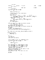
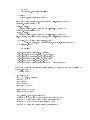
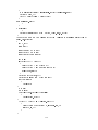
center (nucleus) was not a fundamental unit, but built up by particles called
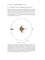
protons and neutrons (Fig. 1). The inner structure of the nucleus was studied
in high energy particle experiments.
Quark -18
size < 10 m
-18
Size <10 m
u
u
e-
d
d
d
u
u
d
d
u
u
Proton, neutron
-15
size 10
m
d
Nucleus,
about 10-14 m
Atom -10
size 10
m
Figure 1: Atom model.
Experiments on the inner structure of nuclear matter have revealed many types
of particles, each with specic well-dened properties, such a mass, electric
charge and intrinsic angular momentum (spin). The best examples are proton
and the neutron, which are the building blocks of the atomic nuclei. The other
particles are short-lived and decay to the more stable protons and neutrons,
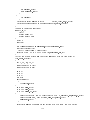
or to electrons. In 1964 the physicists postulated that many of the particles
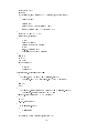
observed in the experiments are built up by smaller objects called quarks. Only
the particles classied as leptons are not built from quarks (Fig. 2).
2
Q U A R K S
Electric
Charge
Mass
(GeV )
Symbol
c2
Name
~ 175
1.5
-3
4x10
2/3
"charm"
"top"
4.7
-3
7x10
0.15
d
"down"
-1/3
t
c
u
"up"
b
s
"strange"
"bottom"
L E P T O N S
Electric
Charge
0.51
-1
0
< 17 eV
c2
e-
105.66
electron
< 0.27
υe
electronneutrino
1784
µ-
τ
-
tau
muon
υµ
< 35
muon-neutrino
Mass
(MeV )
Symbol
c2
Name
υτ
tau-neutrino
Fundamental Forces In Nature
Gravitational Electromagnetic
Weak nuclear
Strong nuclear
Mass
Electric
Charge
+
W-
foton
gravitino
Relative
Strength
Gauge
Boson
-38
10
g
10
-2
γ
Z
(GeV )
c2
80.60
91.16
gluon
-13
1
o
W,+ W, Z
g
10
Figure 2: Quark model.
We now know that there are at least six varieties of quarks, they occur in three
pairs of increasing mass. The lightest pair of quarks, u (for 'up') and d (for
'down'), form the protons and neutrons. The remaining four quarks, form heavy
particles which decay quickly to the lighter particles, as the quarks themselves
transmute to lighter types.
The four heavier quarks carry properties that are not seen in our world of u
and d quarks. For example, the s quark carries one 'negative' unit of a property known as strangeness. In similar way the c, b and t quarks carry their own
unique properties. All the quarks has their anti quark with the opposite charge,
with the same mass. Also leptons has their anti particles.
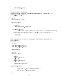
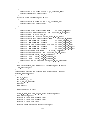
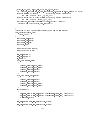
Experiments indicate that quarks can not exist alone. Instead they form clusters, - the baryons and mesons (Fig. 3). The quarks bind together through
the agency of the strong nuclear force.
3
Baryons are clusters of tree quarks. The proton is a baryon. Proton is a
stable baryon and consists of two d quarks and one u quark.
Mesons are cluster of one quark and one anti quark. The pion particle is
a meson.
BARIONS (spin 1/2)
life-time
Protons
uud
25
>1.6 10
Neutrons
udd
Σ+
uus
Λ+c
udc
MESONS
ο
ο
D, D
π +, π −
889 year
-16
0.799 10 s
-13
1.9 10 s
(spin 1)
uc, uc
ud, du
life-time
4.2 s
-8
2.603 10 s
Figure 3: Example of the baryons and mesons.
Quarks, like leptons, have an intrinsic spin angular momentum of 1/2. In
forming particles, the spin of the quarks can thus align in dierent ways. In
the case of baryons (three quarks), the arrangements of two spins parallel and
one anti parallel gives the states of lowest energy (the ground state), that is the
particle with lowest mass. Baryons in which the spins of the three quarks are
parallel have lighter mass. Similarly, mesons with anti parallel quark and anti
quark spin have lower mass than those where the spin is parallel (ref. [16]).
2.1.1 Forces and their particles
Physicists have identied four fundamental forces in nature.
Gravitational
Electro-weak
Weak nuclear
Strong nuclear
They are thought to operate through the agency of particles called gauge bosons.
A particle of matter, such as a quark, feels a force when it receives a gauge boson,
4
carrying energy, momentum and other properties emitted by another particles.
The particles interact via the gauge bosons, as the players in a game of rugby
interact as the they pass the ball.
Electromagnetic . The interaction particle is a photon, . It is a interaction
between electrically charged particles, both quarks and leptons. This is
the force that holds atoms and molecules together.
The strong nuclear force . Interaction particles gluons. These strong forces
acts between quarks and holds mesons and barions together. Energic
quarks can radiate gluons.
The weak nuclear force . Interaction particles are W and Z o. They are
responsible for the decay of quarks and leptons to lighter form which are
less energetic and therefore more stable. This force underlies radioactivity
and reactions that heats the sun and other stars.
Gravitational force . Interaction particles are the gravitons. They are the
weakest of the four powers, and holds matter together in bulk in planets,
stars and galaxies. The graviton has not been observed.
There exist an successful electro-weak theory, which combines the electro-magnetic
and weak forces. So-called 'grand unied theories' that incorporate the strong
force into electro-weak theory have not so far provided entirely successful. They
generally predict that protons should decay on a time scale of some 1032 years,
but there is no clear evidence for this. The inclusion of gravity in unied theories
presents still more fundamental diculties (ref. [16]).
2.1.2 The experiments
The quarks and leptons are very small, certainly less than 10?15 mm across, so
we can not see them directly. To investigate them, physicists employ an armory
of techniques, which reveal the tracks of particles and the products from their
collisions and interactions at high energies. The particles are driven to high
energies in the accelerators (ref. [16]).
2.2 CERN
CERN was commissioned in 1953 by the 12 countries of the Conseil Europeen
pour la Recherche Nuclaire. CERN's main object is to provide european physicists with accelerators that meet research demands at the boundaries of human knowledge. In the quest for higher interaction energies, the Laboratory
has played a leading role in developing colliding beam machines. Notable
'rsts' were the Intersection Storage Ring(ISR) proton-proton collider commissioned in 1971, and the proton- anti-proton collider at the Super Proton Synchrotron(SPS), which became operative in 1981 and produced the massive W
5
and Z particles two year later, conrming the unied theory of electro-magnetic
and weak forces.
The main impetus at present is from the Large Electron-Positron Collider(LEP)
where measurements unsurpassed in quantity and quality are testing our best
description of sub-atomic nature, the Standard Model, to a fraction of 1 percent soon to reach one part in a thousand. This year, the LEP energy will be
doubled to 90 GeV per beam (ref. [13]).
2.2.1 LHC (Large Hadron Collider)
LHC is the latest instrument in Europe's particle physics armory. This great
instrument is needed, because all evidence indicate that new physics, and answers to some of the most profound questions of our time lie at energies around
1 TeV. It is designed to share the 27-kilometer LEP tunnel, and will be fed by
existing particle sources and pre-accelerators. A challenging machine, the LHC
will use some of the most of advanced super-conducting magnets and accelerator technologies ever employed.
LHC can collide proton beams with energies around 7 on 7 TeV and beam
crossing points of unsurpassed brightness, providing the experiments with high
interaction rates. It can also collide heavy ions such as lead with total collision energy in excess of 1,250 TeV, which is much higher than any other Ion
Collider. Joint LHC/LEP operation can supply proton-electron collisions with
energy levels of 1.5 TeV. It will allow scientists to penetrate further into the
structure of matter and recreate the conditions prevailing in the Universe just
10?12 seconds after the "Big Bang" when the temperature was 1016 degrees.
(ref. [13]). The planned high luminosity detectors in the LHC ring are :
ATLAS : A Toroid Large hadron ApparatuS.
CMS : Compact Muon Solenoid. For muon physics.
These detectors have been optimized for the search for the SM Higgs boson
over a mass range to 1 TeV. In addition the detectors have been optimized for
a wide range of new studies :
- Super-symmetric particles
- An extended Higgs-sector
- studies of CP-violation
- new Gauge-bosons
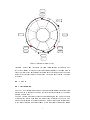
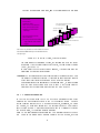
and Standard Model gauge couplings. The basic layout of the LHC is eight
long straight sections, each approximately 500 meters in length, available for
experimental insertions or utilities (Fig. 4). Two high luminosity proton-proton
experiments are located at diametrically opposite straight sections, Point 1
(ATLAS) and Point 5 (CMS). Two more low-beta insertions are located at
Point 2 (ALICE, Pb ions) and Point 8 (B-physics), which also contain the
two injection systems. The beams crosses from one to the other side at these
four locations. The remaining four long straight sections do not have beam
6
Low Beta
(pp)
CMS
Dump
n
6 Octan 7
Cleaning
8
Cleaning
ta
Octan 3 O
ct
an
Oc
4
Octan 5
n
Oc
ta
ta
n
Oc
2
Octan 1
ALICE
LHC-B
Low Beta
Injection
Injection
B-physics
ATLAS
Low Beta
(pp)
Figure 4: Schematic layout of LHC.
crossings. Point 3 and 7 are used for beam 'cleaning' and collimation. The
role of the cleaning is to allow for collimation and cleaning of the beam halo in
order to minimize the background in experiment detectors as well as the beam
losses in the cryogenic part of the machine. The beam abort system is located
at Point 6.
2.3 ATLAS
2.3.1 Introduction
The ATLAS Collaboration proposes to build a general-purpose proton-proton
detector which is designed to exploit the full discovery potential of the Large
Hadron Collider (LHC).
The LHC oers a wide range of physics opportunities, among which the origin
of mass at the electro-weak scale is a major focus of interest for ATLAS. The
detector optimization is therefore guided by physics issues such as sensitivity
to the largest possible Higgs mass range. Other important goals are the search
7
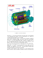
Figure 5: The ATLAS detector
for heavy W- Z- like objects, for super-symmetric particles, for compositeness
of the fundamental fermions, as well as the investigation of CP violation in
B-decays, and detailed studies of the top quark.
The most prominent issue for the LHC is the quest for the origin of the spontaneous symmetry-breaking mechanism in the electro-weak sector of the Standard
Model (SM). New direct experimental insight is required to advance in one of
the most fundamental questions of physics which is closely connected to this,
namely : What is the origin of the dierent particle masses ?
One of the possible manifestations of the spontaneous symmetry-breaking mechanism could be the existence of a SM Higgs boson (H), or a family of Higgs
particles (H, h, H and A) when considering the Minimal Super-symmetric
extension of the Standard Model (MSSM). The Higgs search is therefore used
as a rst benchmark for the detector optimization.
In particle collider concept we use a term called . This term denes at which
angle the detector is able to measure the resulting particles or photons after a
8
collision.
= ln(tan( 2 ))
(1)
Spheric coordinates are used to describe the detector0s geometry. The angels
are expressed in radians. The z-axis is along the pipeline. If we assume that
the inner detector covers to = 2.5, it means that the direction is covered
to 9:4 (ref. [12]).
The ATLAS detector will be built of following sub-systems.
Magnet system . The magnet conguration is based on an inner super-
conducting solenoid around the inner detector cavity, and large superconducting air-core toroids outside the calorimeters.
Inner Detector . Pattern recognition, momentum, vortex measurements, and
enhanced electron identication are achieved with a combination of discrete high resolution pixel and strip detectors in the inner part and continuous straw-tube tracking detectors. The inner detector is contained
within a cylinder , 6.8 m long and 1.15 m in radius, with a solenoidal
magnetic eld of 2 Tesla.
Calorimetry part . This high performance system must be capable of reconstructing the energy of electrons, photons and jets, as well as measuring
missing transverse energy.
There are two types of calorimeters :
1) E.M. calorimeter (Electro-magnetic calorimeter). This is used to identify and accurately reconstruct electrons, photons and leptons over a energy range of 2 GeV to 5 TeV. Many important processes in physics, such
as the decay of bosons into photons or electrons, or the detection of new
gauge bosons decaying to electrons, place stringent requirements on the
E.M. calorimeter in terms of acceptance, dynamic range, particle identication, energy resolution, and direct measurement. This calorimetry will
cover the region j j < 3.2.
2) Hadronic calorimeter. The major goals of hadronic calorimetry at
the LHC are to identify jets and measure their energy and direction, to
measure the total missing transverse energy, and to enhance the particle
identication capability of the E.M. calorimetry by measuring quantities
such as leakage and isolation. This calorimeter is made as end-caps in the
region 1.5 < j j < 3.2 and forward calorimeter in the region 3.2 < j j <
4.9.
Moun Spectrometer . The calorimeter is surrounded by the muon spectrometer. The air-core toroid system, with a long barrel and two inserted endcap magnets, generates a large eld volume and strong bending power.
An excellent muon momentum resolution is achieved with three stations
of high-precision tracking chambers.
The main component of the muon spectrometer is a system of three
large super-conducting air-core toroid magnets, precision tracking detectors with 60 m intrinsic resolution, and a powerful dedicated trigger
9
system. Emphasis is given to reliable, high resolution, stand-alone performance over energy range of 5 GeV to 1000 GeV. Good momentum
resolution is essential for the detection of decays containing muons, above
large backgrounds.
2.3.2 Inner detector
The inner detector is reconstructed to satisfy following specications :
High tracking eciency.
High electron-nding eciency.
High photon-nding eciency.
The layout of the inner detector aims to meet the above goals by applying a
consistent design concept over the whole acceptance. This is achieved by use of
a combination of a few high-precision, high-granularity layers in the inner part
of the tracker, and straw tubes in the outer part which supply a large number of measurement on the track trajectories. This concept oers the benets
to pattern recognition of a device which makes a large number of 'continuous'
track measurement over a long track length, as well as those of a smaller higherprecision points.
The large track density requires the use of tracking layers with high granularity, and the momentum-resolution and spatial-resolution targets demand a high
precision per point in both coordinates. Semiconductor devices on silicon oer
such resolution. A combination of pixel detectors and small-angle stereo-strip
tracking provides the required granularity.
However, such 'precision' layers must be equipped with local electronics, which
results in the presence of extra material and power dissipation in the tracker
volume, and high cost per unit area. This means that the total number of
precision layers must be limited. The layout of precision tracking is such that
every track within < j j < 2.5 crosses two layers of pixels and four strip layers.
Pixel detectors, are used nearest to the beam pipe. The ATLAS pixel
system includes two barrel layers and eight disk layers to provide at least
two tracking points within j j 2.5. These provide two-dimensional
spatial information for pattern recognition.
Strip detectors , are used for the larger-area precision trackers. High precision is obtained in the direction in both the barrel and in the forward
regions. Silicon detectors are foreseen in the barrel and forward region.
The pixel and silicon detectors together compromise the Semi-Conductor
Tracker (SCT). Each semiconductor-strip layer consist of two single-sided
detectors glued back-to-back to measure alternating combinations of 10
Figure 6: Inner detector.
11
and , or and v for the barrel, or combination of and v for the GaAs
forward disks. A precision point may therefore consist of a single pixel
hit, a pair of coordinates from the semiconductor strips.
The inner detector is made of dierent detectors like
TRT , The combined straw tracker and transition-radiation detector, TRT,
provides tracking and contributes to the electron identication over the
whole inner detector rapidity coverage. Its pattern-recognition capability
is strong due to the large number of measurement points, which will be
combined to perform the momentum measurement together with the SCT
precision detectors. The TRT can also provide a stand-alone momentum
measurement, but with a lower precision than the whole inner detector.
Layers of 4 mm diameter cylindrical drift tubes (straw detectors), are
interleaved with radiators to produce and detect X-ray emission from very
relativistic particles. The straw orientations are chosen to make optimal
use of the 2 T axial magnetic eld. The detector will be built in three
dierent blocks - two end-cap TRTs with radial straws and one barrel
TRT with axial-oriented straws. Hence, the barrel TRT measures R
while the end-cap TRT measures and z .
SCT , Semi-Conductor Tracker. The main requirement for SCT are to provide powerful track-nding and pattern-recognition performance, a sagittal resolution of 25m, a polar-angle resolution of 2 mrad.
(Fig. 6)
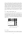
2.3.3 SCT
SCT are made of six barrel layers, two pixel layers in the center and four silicon
layers as shown in gure 7. The design of the SCT is a compromise between
two considerations :
- Minimize the amount of material, cost and hence the number of layers and
readout channels.
- Maintaining an adequate number of layers and readout granularity to facilitate
track nding at high luminosity and within jets at lower luminosity.
The pixel layers . The pixel system is chosen because of their extremely
good spatial resolution information for pattern recognition. The pixel
size is chosen to be the smallest allowed by the area required for readout
electronics. The pixel aspect ratio is chosen to improve the resolution
by the charge sharing, while maintaining excellent z segmentation. The
pixel system is composed of small modules precisely mounted on a stable
mechanical system that must also provide cooling to operate the silicon
detectors near 0C. The readout electronics chips are bumb-bonded directly to silicon detectors.
12
Figure 7: SCT.
The Silicon-strip detector layers . These layers stands for the central pre-
cision tracking. A total of 11 424 single-sided silicon-strip detectors is
required for the four outermost barrel layers.
A guiding principle has been to make the detector highly modular and to
minimize the number of dierent components required. All four cylinders
are built from identical modules, z-modules or R-modules. Each module
consisting of two pairs with readout strips aligned along the z axis; the
other rotated by 40 mrad. In one proposed assembly scheme, 14 modules
are rst mounted onto a stave and then the staves are assembled into
cylinders. Alternate cylinders are built of u ? and v ? layers. A total
of 2856 modules will be required.
In the forward direction a similar number of modules are mounted on
forward disks.
Barrel region . The engineering requirements of the barrel are to :
Support 41 m2 of pixel and silicon detectors with a stability at the
10m level in R, at a constant temperature.
Support 50000 straw tubes for the TRT detector with a stability of
30 m level in R.
Remove up to 20 kW of heat generated by local electronics by using a unied uid-cooling system. The pixels and silicon detectors
operate at a stable temperature of ?7 C with a tolerance of less
than 1 C. The TRT operates at the detector ambient temperature
of 20 C. A thermally-insulating enclosure, with a ow of cold
13
dry nitrogen, will be required around pixel and silicon detectors to
prevent condensation.
Figure 8: Silicon barrel at R= 60 cm.
In the forward direction the requirements are similar.
The cooling system . There are two major problems that each cooling concept has to address.
(1) The front-end electronics produce a well localized large power density
which has to be removed before it can heat up the silicon detectors. The
available surface area for cooling is small (less than 1 cm2 per chip and
very delicate).
(2) The silicon detectors also dissipate power. This is exponentially dependent on the temperature. The power is spread across a large area,
and due to it's temperature dependence, the power dissipation is largest
in those places which are hottest. This may lead to a situation where the
silicon detector thermally runs away in a badly cooled area.
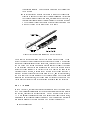
Two designs are being pursued for the silicon strips mechanics and cooling
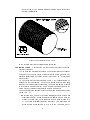
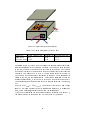
system (Fig. 8):
Beryllium rods, with built-in cooling channels, are used as the main
structural element. Silicon modules are mounted directly onto the
binary-ice cooled rods, which results in a short thermal path (Fig.
9). These are interconnected using four rings. This structure must
accommodate movements up to 0.5 mm in the z direction, due to
14
temperature changes. This rod-based solution is most suitable for
the Z-module.
The second scheme is based on the use of composite cylinders constructed to have a zero coecient of thermal expansion. In this case
the cooling pipes are clipped into place, but are allowed to move in z ,
thus avoiding transmission of thermal strains to the silicon modules.
A good thermal contact is provided by a heat-sink compound. This
method of cooling will be used for the R-module.
Figure 9: Beryllium stave equipped with the z -module.
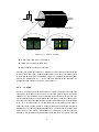
The module is the basic building block of the silicon detector system. It consists of two pairs of daisy-chained detectors glued back-to-back. Two dierent
topological congurations are being prototyped, these are the R-module and
the Z -module. The second option uses beryllia fan-ins to connect the strips
to the front-end chips which are mounted on the side of the module directly
above the cooling channel. The cooling for the R-module is the same as the
one used for the z-module, to attach the R-module to the cooling pipe line. A
single R-module is glued on to a cooling plate (Fig. 10), and this cooling plate,
the R-module on it is then attached to the cooling pipeline. The cooling uid
arrives in the cooling pipeline, the cooling plate will then be cooled down. The
cooled plate will then cool down the front-end electronics and the detectors.
2.3.4 R-module
In the R-module , the front-end chips are mounted on top of the silicon detectors. This is natural conguration for the electrical connections but complicates
the cooling, especially for a stave solution. The R-module is shown in Fig.
11. It is a natural conguration to use with axial or small angle stereo strips,
particularly on a cylindrical support structure. This is because the electronics
are oriented parallel to the strip direction. The module is designed to :
Be self supporting.
15
Y
R
φ
θ
Z
X
SILICON BARREL
Or
Cooling plate
Cooling pipe
R φ -Module
Z-Module
Cooling pipe
With new
cooling
Concept.
Figure 10: Z - and R-module
Minimize the number of components.
Maximum the signal-to-noise ratio.
Have open edges for ease of overlap.
The last tree points are realized by placing the front-end electronics near the
middle of the module unit. Reading signals out at the middle of the strips results
in the minimum noise and the maximum signal. This because the resistive input
load on the preamplier is 1/4 of the load with readout at the ends and the
signal dispersion through the strips is also reduced.
2.3.5 Z -module
On the Z -module beryllia fan-ins are used to connect the strips to the front-end
chips which are mounted on the side of the module directly above the cooling
channel. The detectors and the hybrid assembly are adjent to each other. The
cooling runs along the hybrid in z and makes contact between the readout chips.
The front-end electronics and silicon strips are interconnected by berylla fan-ins
(Fig. 12) which also serve to cool the detectors. Detectors are either back to
back single sided or double sided. The hybrid supports the front-end electronics
and provides the control,readout and bias lines. The front-end chips are placed
on both sides of the hybrid. One advance of this design is that the front end
electronics are decoupled electrically and thermally from the silicon. Another
16
60
120
Be compression plate
Kapton hybrid
Si 0.3 x 60 x 60mm3
Spacer
Be shield
Carbon spacer
2mm
Be shield
Be cooling plate
10mm
Cooling pipe
Figure 11: R-module.
advantage is that the cooling paths are short into the detectors. This geometry
provides optimal connectivity to services and as mentioned, ecient cooling.
2.3.6 Silicon-strip readout electronics
The requirements on the electronics and, in particular, on the front-end electronics can be summarized as follows:
The total noise after 10 years of operation should be less than 1500 elec-
trons equivalent noise charge (ENC), giving a signal-to-noise ratio (S/N)
above 12:1, in order to maintain high eciency and low noise levels compared to the hit rate from particles. Results obtained in the test beam,
using prototype LHC readout, indicates that a pulse-height threshold on
single strips, would be viable if these specications are met.
Power per unit area of detector < 40 mW cm?2.
Maximum signal of 6-8 minimum ionizing particles (mips).
17
Figure 12: z -module.
De-randomizing buers to assume < 0.1 percent data loss for maximum
mean rst level trigger (T1) at 100 kHz.
Operation with a 2 s rst level trigger latency.
Full functionality after exposure to 100 kGy of ionizing radiation and
21014 n cm?2 .
System design tolerant to the failure of any single circuit element.
Three separate approaches (Analog, Digital and Binary) to the development
of electronics , design have been followed. In all schemes, detector signals are
amplied, shaped, and stored in on-detector pipelines until a read request is
prompted by rst level trigger (T1). At that point either analog, digitized analog or binary data are transferred using optical links to the o-detector readout
buers.
In the analog architecture, a preamplier is followed by an analog pipeline, a
fast analog multiplexer, and optical analog readout of all pulse heights.
Prototypes for both the analog and binary options have already been evaluated
in test beams and have been shown to have the good noise performance. For example, a bipolar preamplier/shaper circuit has a measured noise performance
of 391e? + 27e? /C, where C is the capacitance in pF, at a power consumption
of 1.61 mW per channel and with a peaking time of 23 ns. (ref. [1]).
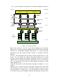
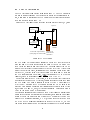
2.3.7 Trigger System
The ATLAS trigger is organized in tree trigger levels (LVL1, LVL2, LVL3), as
shown in Fig. 13.
18
At LVL 1, special-purpose processors act on reduced-granularity data from a
Latency
Rate [Hz]
CALO
MUON
TRACKING
40 x 10
pipeline
memories
LVL1
~2 us
(fixed)
LVL2
6
4
5
2
3
1
2
10 - 10
derandomaizing
buffers
MUX
MUX
MUX
digital buffer
memories
~1-10ms
(variable)
10 - 10
Readout/ Event Building
~1-10GB/s
Switch-farm
interface
LVL3
(processor
farm)
10 - 10
Data Storage
~10-100 MB/s
Figure 13: The Trigger System.
subset of the detectors. The LVL2 trigger uses full-granularity, full precision
data from most of the detectors, but examines only regions of the detector identied by LVL1 as containing interesting information. At LVL3, the full event
data are used to make the nal selection of events to be recorded for o-line
analysis.
The LVL1 trigger accepts data at the full LHC bunch-crossing rate of 40 MHz
(every 25 ns). The latency (time taken to form and distribute the LVL1 trigger
decision) is about 2 s, and the maximum output rate is limited to 100 kHz by
capabilities of the sub-detector readout systems and the LVL2 trigger. Hence,
the LVL1 trigger must select no more then one interaction in about 104 (one
bunch crossing in 400).
Muon and calorimeter trigger conditions are evaluated in separate LVL1 processors.
During the LVL1 trigger processing, the data from all parts of the detector are
held in pipeline memories. The LVL2 trigger must reduce the rate from up to
100 kHz after LVL1 to about 1kHz. LVL1 trigger system is used to identify
the regions of the detector containing interesting features such as clusters (elec19
trons/photons), jets and muons. LVL2 trigger then has to access and process
only a small fraction of the total detector data, with corresponding advantages
in terms of the required processing power and data-movement capacity.
The LVL2 trigger uses full-precision information from the inner-tracking, as
well as from the calorimeters and muon detectors. After an event is accepted
by the LVL2 trigger the full data are sent to the LVL3 processors via the event
builder (EB). Complete event reconstruction is possible at LVL3, with decision
times up to about 1 s. The LVL3 system must achieve a data-storage rate of
10-100 MB/s by reducing the event rate and/or event size. (ref. [1]).
20
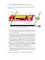
3 The prototype units for the ATLAS SCT
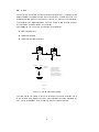
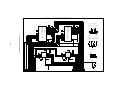
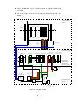
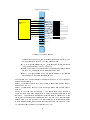
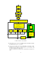
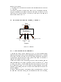
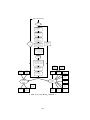
For the ATLAS SCT test-setups, following units for silicon-strip detector readout are used. (Fig : 14).
Strip Detector
Strip#32
Strip#2
Strip#1
MUX32
FElix32
11
00
00
11
00
11
00
11
00
11
00
11
00
11
00
11
00
11
BUFHOLD
CH#32
RBIT
CH#32
CH#2
CH#1
A
CH#2
CH#1
SF
BUFCLK
DFF
V
bias
OUT
111111
000000
000000
111111
000000
111111
000000
111111
000000
111111
000000
111111
000000
111111
000000
111111
RESETB
SF : Source Follower
DFF : D flip-flop
B : Output Buffer
Hybrid
PCB
Figure 14: The Front-end electronics.
Silicon-strip detectors. When a particle crosses the detector, it will release
some electrical charge, the charge drifts in the electric eld to the output
of the corresponding strip.
FElix , front-end chip. This chip contain several channels. Each channel
amplify and shape the signals coming from the corresponding strips of the
strip detector. The amplied signal in all channels are sampled by the
FElix, and sent to the outputs when a rst level trigger, T1, is received.
MUX , the multiplexer. The analog signals from the each channel of FElix
outputs are connected to the inputs of the MUX. The MUX will convert
the parallel signal coming from the FElix into a serial output sequence.
Hybrid . The front-end chips are mounted on this board. The chips are
connected together through the several hybrid layers. Many layers are
used to reduce the pickup noise on the the control- and power lines and
several layers are also needed for all the interconnections.
PCB . This is a support Printed Circuit Board for the hybrid. This
board function as the interface between hybrid and the VME system.
The signals from the front-end chips on the hybrid are send for further
analysis through the PCB.
All these modules are described in more detail in the following sections.
21
3.1 Silicon micro-strip detectors
Strip detectors are widely used for reconstructing the particle paths in the particle detectors. The ATLAS experiment being designed for the CERN LHC
will include a large micro-strip tracking detector. This detector must operate
in a high radiation environment for at least 10 years, maintaining a satisfactory detector performance despite the resulting severe changes in the material
properties of the silicon and dielectric.
The ATLAS tracker requires one 'barrel' detector design for the majority of
the silicon wafers and ve slightly dierent designs for the 'forward' detectors
which are to be built into disks. The same specications apply to all designs
except for the small geometrical dierences required for the 'forward' detectors.
The nal overall production requirement for the ATLAS will be for about 20
000 detectors (ref. [14]).
3.1.1 The properties
In silicon one gets an electron-hole pair for every 3.6 eV released by a particle
crossing the medium. The radiation sources sends the electrons at least 1
MeV. An other sensitive eect of the high density silicon is the high energy
eV . It give
loss of the incoming particle , the average energy loss is about 290 m
. There is no multiplication of the primary charge and
about 80 elec?holepairs
m
the collected signal is only a function of the thickness of the detector. The
practicle thickness limit is set by the signal to noise ratio and the thickness of
the depletion zone.
Silicon is an element of the group 4 and have 4 electrons in the valence shell.
The p- and n-type materials are obtained by replacing some of the silicon atoms
by atoms from group 3 or 5 respectively. The elements from group 5 are called
the donors, they have 5 electrons in the valence shell. This is called n-type
material and the majority carriers is the electrons. Doping atoms from the
atoms from group 3 is called the acceptors, in this p-type material the majority
carriers are the holes.
In both the p- and n-type materials the carriers of the other type, the minority
carriers, coming from the thermal excitation of silicon atoms. The densities of
electrons and holes in a semiconductor is given by
Ec ?Ef )
kT
n = Nc exp?
(
p = Nv exp?
(
(2)
Ef ?Ev )
kT
where Nc and Nv are eective densities of state at the conduction and valence
band edge respectively. Ec ; Ef and Ev are the energies of the conducting band,
Fermi level and the valence band, k is the Boltzmann constant and T is the
temperature.
22
Intrinsic carrier density, ni is
Eg
ni 2 = np = NcNv exp? kT
where Eg is the energy gap given by Eg = Ec ? Ev . For silicon, Eg = 1.1 eV at
room temperature.
The conductivity, , is given by
= eni(e ? h )
and the resistivity is just the inverse of .
Since the semiconductors are neutral, the negative and positive charge must be
equal
ND + p = N A + n
ND ; NA is donor and acceptor concentration. In n-type material NA=0 and n
>> p density, then n = ND
.
3.1.2 The silicon detector basic principle
N
P
+
-
-
+
+ + +
+
+ - -
-
Donor ion
+- - +
+- +
+
- + + +
+
Acceptor ion
- Electron
+ Hole
A depletion layer is
formed on either side
of the junction.
+
-
- +
-+
- -
w1
+
+ +
+
- --
- +
- -+
+
- + + +
a)
w2
b)
Dopant
concentration
c)
Space charge
density
x
d)
Carrier
density
x
e)
Electric
field
x
f)
Electric
potensial
x
x
Figure 15: pn junction.
23
Net charge density
showing zero charge
except for a dipole
layer at the junction.
Electron and hole density
through the crystal showing
no free carriers in the
depletion zone.
The principle of the operation of a silicon radiation detector is to deplete the
detector of free carriers through a reverse biased p-n junction. Depleted of free
carriers it behaves like a capacitor, drawing little current under the applied
voltage, but any charge deposited within its volume drift towards the junction
and can be collected. The particle detectors are made of high resistivity materials.
There is some built in potential, of the order of a few hundred V , between the
junctions.
If we regard the junctions as a detector, one sees that the charge created in the
depleted region by a transversing particle could be collected at the junctions
and read out. Charge created in the neutral, non-depleted zone recombines
with free carriers, and is lost. Increasing the width of the space charge region
(depleted zone), increases the collected signal. Ideally one would like to have
the hole thickness of the n-type silicon depleted of free carriers. It is possible by
applying an external potential dierence, Vbias , of the same sign as the builtin
potential, Vd . The barrier height would be given by VB = Vbias + Vd. The
junction is reverse biased.
The depletion width, w, is given by
w = w1 + w 2
where
w1
and
w2
v
u
t qN 2(1eV+B Na )
=u
a
Nd
d
Na
v
u
t qN 2(1eV+B Nd )
=u
Na is the acceptor concentration and Nc is the donor concentration.
Here we can see that the width of the space charge region depends on the reverse bias voltage, VB and the acceptor, donor concentration in the pn junction.
By increasing the VB the width can be increased.
A silicon strip detector is a p or n junction called bulk, with highly doped n or
p strips at the surface of bulk. Under the bulk is placed a highly doped n or
p plane for applying the Bias voltage. As shown in the Figure 15, there are
some guard-rings around the strips, these rings are used to protect the strips
from leakage from the detector edges. The guard rings are usually connected
to ground. The rings are incorporated to promote higher voltage operation.
3.1.3 The spatial resolution.
The resolution of the silicon micro strip detectors depends on many factors
which can be divided into two categories. The rst contain physical processes
like statistical uctuations of the energy loss. The second is the external parameters like strips, readout pitch and the electronics noise. However taking all
24
Read out
Pitch
Strip
width
Guard-rings
Thickness
h+
SiO2
p silicon strip.
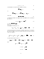
+ -+ e+ +-
n-type silicon bulk
n+silicon. (Back plane, V bias> 0)
Schematic of a silicon particle detector.
Figure 16: Silicon detector.
these constraints into account one can improve the precision and a localization
precision as good as 1.0 m can be achieved.
For events generating signals on just one strip, the track position is given by the
readout pitch. For events generating signal on two strips one can measure the
position more precisely by calculating the center of gravity. The best location
accuracy will be obtained for tracks crossing the detector between two strips
because the signal is equally shared on both of them and the inuence of noise
is small. The localization precision for tracks close to a strip is bad because the
noise is relatively important for the small signal on the neighbor. (Ref. [5]).
25
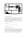
3.2 FElix
The FElix chip is designed to read out strip detectors at LHC. It provides a fast
analog signal at the output when a trigger is received 2 s after the event. The
signal output can either be the peak of 75 ns CR-RC pulse or of a (processed)
25 ns peaking time triangular pulse. The chip is said to run in 'peak mode' or
'de-convoluted mode' according to the output.
One channel in the FElix chip is composed of three parts:
Front-end amplier.
Analog data buer.
Analog pulse signal processor.
C
R
fp
fp
C
-
I
in
fs
R
fs
-
+
Source
C
V preamp
+
V out
Drain
MOSFET
transistor
Gate
V
R
fp
A mostfet transistor
is used as a resistor.
The resistor value is
regulated by regulating
the Vfs. The edges of
the resistor are source and
f=drain on the transistor.
fp
SOURCE
Source
Figure 17: Pre-amplier and shaper
The idea behind the design of the FElix chip was to keep the front-end power
to a minimum level, and at the same time retaining the speed necessary for
LHC timing. Standard CMOS technology is used to make this chip.
26
First level Trigger
T1
Input Signal
40 MHz
YES
Buffers
Sample
&
Hold Unit
Pre-amplifier
&
Shaper
NO
1.775 us delay
analog pipeline
Garbage
AMPLIFIER
ANALOG DELAY AND BUFFERING UNIT (ADB)
Signal height of shaped samples
Buffering
And
Amplification
+
+
APSP
35 ns/bin
ANALOG PULSE SHAPE
PROCESSOR
Time
Max Out
+
Weighted sum
performs
Deconvolution
APSP Out
Figure 18: A single channel of the FElix
3.2.1 Front End Amplier
This is the analog part of the FElix. The pre-amplier is a current-to-voltage
converter. The charge-sensitive pre-amplier has a gain of 1 mV/fC. The amplier has PMOS input device and a feedback capacitor of 0.75 pF (Fig. 17).
It is designed to run at 700 A current between 2 V. This gives a power
dissipation of 1.4 W. The pre-amlier and the shaper both give an overall
CR-RC shape with 75 ns peaking time. The noise slope has a function of load
capacitance given by this equation.
ENC = (220 + 27:5=pF )electrons
for peak mode, and
ENC = (500 + 60=pF )electrons
for de-convoluted mode.
3.2.2 Analog data buer (ADB)
Full read-out of millions of strips at a rate of 40 MHz, would be a impossible
task. Therefore the pipeline is needed to store the data until a rst level trigger
arrives. The ADB is divided into the actual pipeline which is 84 cells long and
the control logic which controls the overall timing of the pipeline and buering
mechanism. The input signal is continuously sampled by the Sample and Hold
unit which samples at rate of 40 MHz. These samples are then stored in the
27
pipeline. The samples travels through the pipeline, and when the pipeline is
full it starts to ll the pipeline from the start again. When the rst level trigger
arrives, four samples are tagged and protected from overwriting and becoming
buers. There are four such buer zones, one for each event. A total of 16
cells are used by four events. The stored events are read out sequentially, rst
in rst out. At the arrival of the rst level trigger, T1, the rst three of the
four samples are sent to APSP to produce a De-convoluted pulse. The peak is
rst sent on the output for 550 ns and then followed by the de-convoluted pulse
after 250 ns reset period. The de-convoluted pulse remains at the output for
550 ns. T1 can arrive at any time in the CR-RC pulse, the height of the signal
on the FElix output correspond to the value sampled, in the CR-RC pulse, by
the T1.
3.2.3 Analog Pulse Signal processor (APSP)
The APSP implements a nite impulse response lter by taking the three of
the four samples from an event and adding them with dierent weights. The
weights have such values that the sum of tree weighted samples always is zero,
except at the beginning of the CR-RC pulse. APSP unit de-convolute the
CR-RC shaping done by the pre-amplier/shaper and gives an output, that
is proportional to the shaped signal. The de-convoluted pulse have a peaking
time of 25 ns (g. 30). The De-convoluted pulse is then sent out to the FElix
output for 550 ns.
BCO
TR
(Scintillator)
CAL
S3
PEAK-MODE
Pulse from the
particle after
RC-CR shaping.
S2
S1
The RC-CR pulse
after De-convolution
T1
De-covolution :
Y = w1*S1 + w2*S2 + w3*S3
The parameters w1,w2 and w3 are such that the de-covoluted pulse, Y, allways is zero
except for these tree samples. This means that the parameter w1 and w2 have opposite
sign of w3.
Figure 19: The de-convoluted pulse.
3.2.4 FElix32
This FElix version contains 32 channels. In this chip one channel is broken into
its logical units in a way that each of the three blocks could be investigated
28
separately. This chip is designed for use with a 40 MHz clock. A multiplexer
(MUX) is also designed by Jan Kaplon for use with the FElix in lab testing and
beam tests. The MUX readout speed is 5 MHz.
This FElix chip has been successfully used in several beam tests [7].
3.2.5 FElix32 signals
The signals from the FElix can be divided into three groups.
Power supply lines.
Bias current lines.
Control signals lines.
The analog part of FElix, the front-end amplier in each channel is supplied by
the signals AVDD and AVSS. Other parts, Analog data buer (ADB) and the
Analog Pulse Signal Processor (APSP) is supplied by the signals DVDD and
DVSS.
Almost all of the control signals must be CMOS compatible, since the CMOS
technology is driven by 2 V, the logical signal is +2 V for high level and -2 V
for low level. Some of the signals are described in detail below.
VFP, PREB and VFS, SHAB . The analog supply voltages are used to
generate VFP and VFS, because internally in the chips these voltages
are provided to the gate of a MOSFET transistor coupled like a resistor.
The two edges of the resistor are used as source and drain. (As shown
in Fig. 17) By regulating VFP one can change the resistor value in the
Pre-amplier. The Pre-amplier is the integrator part of CR-RC pulse
creating. The PREB current is also used to control the integration time of
the pulse. The resistor in the shaper is controlled by VFS. By regulating
VFS one can control the shape of the pulse. SHAB current is also used
to shape the pulse (Fig. 18).
BUFB . Is the operating current of the Pre-amplier/shaper output buer.
BCO . This is a 40 MHz continuous clock signal to the FElix. The Sample
and Hold unit samples the pulse, coming from the Pre-amplier/shaper,
with the BCO rate and send it to the pipeline. BCOB is the inverted,
DUMMY, signal of BCO, it is just bonded to the FElix and have no
function inside the FElix.
RESETB . Reset signal for the FElix. The FElix must be reset for each readout period. It can be done in the beginning or at the end of a control
signal sequence. It is active low and it has to be held low for 8 clock cycles.
At CERN test-setup this signal is held low at the end of the sequence.
29
T1 . Is the rst level trigger, it must arrive at least within the time vailable
the demanded samples is at the end of the pipeline. This signal is active
high, when the signal is at least 0.5 V. Low is when the signal is less
than -0.5 V. At the arrival of T1 the last four samples in the pipeline are
pulled out and sent to the analog signal processor APSP. The continuous
readout frequency of the FElix is 250 kHz. If several triggers occurs in
short interval the FElix will put them out one at a time at a rate 4 s per
event. Processing a single event will take 4.775 s. The maximum trigger
rate is 100 kHZ. T1B is the DUMMY version of T1.
DTA . This is asserted when there is data ready on the FElix output. In
the old logic there was a DTA pulse which was divided into two by a
reset period of 250 ns. Also, rstly this signal is asserted for 550 ns
indicating that there are peak-data on the outputs. Secondly this signal
is un-asserted for reset before asserting this level again for another 550 ns
indicating that there are de-convoluted data available on the outputs. In
the new logic FElix the signal is also asserted for the while the outputs
are reseted. There can be many groups of the DTA's in a readout period.
This depends on the width of the T1.
BUSY . This signal can by used by the external electronics to slow down the
FElix read-out. The signal can be asserted at any time after one BCO
clock after the rst DTA and 13 BCO's after the second DTA. The FElix
will then nish the read-out of the event associated with these two DTA
pulses and it will not start to read-out any more events before BUSY is
brought low again.
3.2.6 FElix128
The FElix128 is an extension of the previous version to 128 channels, but it
also include several important changes :
Front-end is made faster, on the basis of the results from the 'broken
channel' of FElix32.
The on-chip buer stage between the front-end and the ADB was simplied and referenced to ground instead of an adjustable reference voltage.
Two bias voltages are now generated on-chip instead of using external
potentiometers.
All the control signals enter as ECL levels and are converted on-chip.
The rst change is now shown to be mistaken. From the analysis it can now be
shown that the previous version of the FElix had the correct shaping time [8],
and the problem was related to the output buer of the broken channel.
30
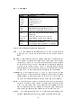
Table 1: FElix32 signals.
Signal
Description
AVDD
Analog power (+2 V)
AVSS
Analog power (-2 V)
DVDD
Digital power (+2 V)
DVSS
Digital power (-2 V)
GND
Ground
VFP
Pre-amplier feedback resistor (-0.4 V)
VFS
Shaper feedback resistor (0.3 V)
VDC
Grounded trough 100 nF capacitor, ADB storage
capacitor backplane.
VBP
Grounded trough 100 nF capacitors,
APSP backplane capacitors.
PREB
Pre-amplier bias current (700 A)
SHAB
Shaper bias current (120 A)
BUFB
Pre-amplier/shaper output buer (80 A)
APSPB APSP bias current (20 A)
BCO
40 MHz clock. At least 0.5 V swing around +0.2 V.
BCOB
Inverted of BCO, implemented to reduce pick up.
RESETB FElix reset. (Active low)
T1
First level FElix trigger.
T1B
Inverted of BCO.
DTA
Data on the FElix output.
DTAB
Inverted of DTA.
BUSY
Digital control input.
CAL
0.07 V step excite all channels from FElix with
1 MIP. Internal capacitor of 56 fF for each channel.
INP1
Analog input to inject a charge in rst broken
channel. 1 MIP for 2 mV step for external
capacitor 1.8 pF.
OUT1
Analog output from preamlier. In rst broken
channel.
OUT2
Output from pre-amp.
in second broken channel.
31
3.3 MUX
A dedicated analog multiplexer chip (AMUX) for the readout of silicon detectors was designed and manufactured, with the same CMOS technology as in
FElix. Data from all the channels in FElix are released at the same time at
the corresponding outputs. The operating computers read out the front-end
electronics serially. The AMUX is used to convert the parallel data from the
FElix into serial data. The outputs of the FElix are bonded to the inputs of the
multiplexer. A clock signal is provided to the MUX for sampling the signals at
the input and the signals are then sent out serially, one by one. The aim was
to design a multiplexer which had following parameters.
- power dissipation less than 50 mW for 32 channels.
- readout-speed 20 Mhz.
- dynamic range of the input 0 - 1 V, with 2 V power supply.
- maximum load capacitance 20 pF, typical 10 pF.
The multiplexer chip contains 32 input channels with Sample-and-Hold circuits.
In addition to the 32 input channels, one extra channel is used to cancel the
oset and the cross-talk from the digital parts. The output from this channel
can be used as a reference for the dierential output. Each channel consists of
an input switch, a storage capacitor and an input buer, designed as a source
follower based on an NMOS transistor biased with 20 A. This bias current is
called SFBI in our test-setup design. With this NMOS technology a slew-rate
of 75V/s is obtained. The multiplexing function is implemented as a simple
array of 32 NMOS switches controlled by a shift register connected by an analog bus line to the output buer. This shift register is controlled by sending a
signal called RBIT. By sending a logical one down trough the shift register, one
enables a new channel switch for each clock-cycle. The bit is clocked in on the
negative edge of the clock. There is also a reset line to the MUX. The MUX
reset signal is active low and this resets the register made by the D ip-ops.
32
3.3.1 The signals
Table 2: MUX signals.
Description
Analog power (+2 V).
Analog power (-2 V).
Digital power (+2 V).
Digital power (-2 V).
Ground.
Bias voltage for pull-up resistor (1 V).
Bias current for output buer (150 A).
Current for sample and hold buer (20 A).
Max. 20 MHz clock for the shift register,
active high.
MRESETB Resets the shift register. (Active low).
HOLDB
Select sample or hold. Hold when low.
RBIT
Input of shift register, active high.
MOUT
The analog MUX output.
OLEV
The reference part of analog MUX output.
Signal
AVDD
AVSS
DVDD
DVSS
GND
MPUL
BUBI
SFBI
CKL
Some of these signals are described in detail below.
CLK . MUX has a maximum operation speed of 20 MHz. When the FElix
is read, the MUX clock must be turned on while the HOLDB signal is
active.
HOLDB . Data is ready on the FElix outputs when the DTA signal from the
FElix is active. To sample these data the HOLDB must be set low inside
the active DTA pulse. MUX will hold the peak-data if HOLDB is turned
low in the rst 550 ns of the DTA pulse and the de-convoluted data when
it is held low in the last 550 ns. The MUX clock can then be started
anywhere inside the active HOLDB signal. This hold signal must be held
low until the MUX has clocked out all the data on the FElix output.
MRESETB . Reset signal for the MUX. The MUX must be reset for each
read-out period. It can be done in the beginning or at the end of a control
signal sequence. It is active low and it is held low for 8 clock cycles. In
the CERN test setup this signal is held low at the end of the sequence.
RBIT . One logical high bit is sent to the rst shift register to get the samples
on the MUX outputs. This bit has to be clocked in on the negative edge
of the CLK. One extra clock cycle is needed at the beginning or at the
end of a read-out period. By sending a logical one down through this
shift-register, one enables a new channel switch for each clock-cycle.
MOUT . This is an output from the MUX. Signals from each channel, with
the same duration as one clock cycle, is send out serially on this line.
33
OLEV . This output is implemented for having a dierential output.
In CERN test-setup a 5 MHz clock was used for the MUX to read out the
32
FElix32. This gives a readout time of 5MHz
= 6:4s. The time it takes to
read-out the MUX is more the minimum time between outputs from the FElix,
which is 4 s. Therefore to read-out the FElix without use of BUSY, a MUX
that can run at 40 MHz, is needed. This is implemented in the new version of
FElix, the FElix128. (Ref. [24]).
34
3.4 Hybrid
For detector read-out in the ATLAS inner detector, front-end electronics with
the following characteristics are needed in the ATLAS inner detector.
Low noice
High speed of operation, accuracy, low power consumption, low weight
and small size
High tolerance for changes in the operation environment, such as uctuating temperature.
Long lifetime with good reliability
To meet all these specications, thick lm hybrid technologies are found to be
most satisfactory. The feature of the thick lm hybrid technologies are high reliability and stability, of both the components and the interconnections compared
to the printed circuit board, PCB, technology. The level of packaging technology is also high, with the capabilities of multi-layer conductor patterns and
printed components integrated in the substrate area underneath the mounted
components. The substrate is made of ceramic and in the PCB the glass/epoxy
laminates are used. These technologies give high frequency characteristics compared to the PCB [9]. The substrate in the hybrid also give other important
properties
High thermal conductivity
High electrical resistivity, giving isolation between components, that reduce the pickup noise from neighboring components.
To reduce the radiation length, thin materials must be used in the detectors and
front-end electronics. The high luminosity leads to the need of radiation hard
technologies both for the detectors and front-end electronics. The Signal-toNoise ratio of the front-end electronics after 10 years of operation is 15. In this
way we can obtain and maintain an eciency above 99 % with and occupancy
below 10?3 and a spatial resolution better than 20 m.
3.4.1 Hybrid for FElix32 read-out
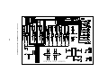
The Hybrid for FElix32 read-out is designed by Bjrn Magne Sundal and Ole
Dorholt at University of Oslo (Figure 20). To reduce the noise, the following
basic rules have been taken into account during the design of the circuit.
Keep the analog and digital signals well separated.
35
Separate power for the analog and the digital parts.
Make power and ground planes separated. Critical signals must be shielded
from each other by means of these planes.
Short tracks are better, because they reduces the capacitance of the tracks
and their ability to pick up nearby signals.
Signals with very fast rise and fall time should have its inverted signals
close to its own track in order to reduce pickup.
The hybrid has a track where the silicon strip detectors backplane can be glued
on the hybrid by leading adhesive [10].
Two connectors, CON 1 and CON 3 are implemented to receive and send the
digital and analog signals between the PCB and hybrid. For the detector power
supply CON 4 is used and CON2 is used for power supply of the FElix and
Multiplexer.
The hybrid for the FElix32 is constructed for two chip-sets (g. 20 and can be
used to read out 64 signals.
36
THE PROTOTYPE HYBRID.
GATE
1
2
3
4
6
5
7
8
9
11
10
12
CON4
DVDD
1
C5
100NF
100nF
CER
2
DECOUPLING
TO POWERPLANES
C6
VBP13
APSPB12
470NF
AVSS
DVSS
AVDD
100nF
CER
2
DVDD
1
1
CD2
CD1
1
100nF
CER
1
CD4
11DVDD
1
470NF
GROUND
BIAS
BUFB18
OUT117
OUT216
VDC15
DVDD214
1
VBP13
APSPB12
BCKPLN
AVDD
1U0F
MKT
DVDD
2
C3
1P8F
AVSS
2
AVSS
3RESETB
4BCOB
5BCO
6DTAB
7DTA
8T1B
9T1
10BUSY
100nF
CER
1P8F
CER
1
C2
100NF
FELIX
2DVSS
DVSS
DVDD
INP127
GND26
CAL25
VFP24
AVSS223
PREB22
AVDD21
20
VFS
SHAB19
2
1P8F
CER
1AVSS
AVSS
BUFB18
OUT117
OUT216
VDC15
DVDD214
1U0F
MKT
11DVDD
AVDD
1
DVDD
1P8F
AVSS
2
100nF
CER
100nF
CER
2
2
2
100
1
1
100nF
CER
100nF
CER
2
2
CVFS
100NF
VFP
CAL
INP1
OLEV2
MOUT2
OLEV1
MOUT1
MPUL
RBIT
CKL
VFS
PREB
BUBI
SFBI
APSPB
RESETB
OUTAMP22
BUFB
OUTAMP21
SHAB
DTAB2
HOLDB
DTA2
MRESETB
T1
T1B
DTA1
DTAB1
BCOB
BCO
1
2
3
4
5
6
7
2
1
3
4
5
7
6
8
9
10
11
12
13
14
15
16
17
18
19
20
21
22
23
24
1
2
3
5
4
6
7
8
9
10
11
12
13
14
15
16
17
18
19
20
21
22
23
24
CON1
CMPUL
100NF
8
1
2
9
CON2
AVSS
CVFP
100NF
100nF
CER
10
DVSS
DVDD
11
AVSS
DVSS
DVDD
12
BUBI13
OLEV12
DVSS7 RBIT9 AVSS
DVDD8
MPUL 11
10
13
BUBI12
OLEV
DVSS7 RBIT9 AVSS
DVDD8
MPUL 11
10
AVSS
AVDD
AVSS
ATST17
AVDD16
15
SFBI14
MOUT
DVSS
1
2TCKL
3TRB
HOLDB
4GND
5CKL
6
MRESETB
AVDD
DVSS
DVSS
17
ATST16
AVDD15
SFBI14
MOUT
MUX
AVDD
1TCKL
2
3TRB
4HOLDB
5GND
CKL
6
MRESETB
TSH
DVDD
MUX
AVDD
TSH
DVDD
DVSS
18
U4
18
nF
POWER
DVSS
DVSS
U3
OUTAMP11
OUTAMP12
37
Figure 20: FElix32 Hybrid.
DVSS
3RESETB
4
5BCOB
BCO
6DTAB
7
8DTA
T1B
9T1
10BUSY
C4
1
2DVSS
2
DVSS
1AVSS
FELIX
AVSS
FOR THE
DETECTOR PART
U2
C1
INP127
GND26
CAL25
VFP24
AVSS223
PREB22
AVDD21
20
VFS
SHAB19
CD3
U1
CON3
B.M.SUNDAL, UiO, jan. -95
3.5 PCB for Hybrid
The PCB used in the test setup is a simple double layer PCB with conductor
pattern on each side of the board. The PCB was constructed at University of
Oslo to support the hybrid in the test setups at the University of Oslo [10].
All the signals from the PCB to Hybrid are sent through Dupont connectors
by Kapton cables. Power supplies to the PCB and the Hybrid are supplied
through the connector CON5. The PCB is shown in gure 21.
All the biasing currents to the FElixes and MUXes on the Hybrid are generated by potentiometers on the PCB. These currents are generated by the
AVDD power line via a potensiometer. The bias-currents are sent through the
connector CON3 on the PCB to the corresponding connectors on the Hybrid.
The voltages Vfp and Vfs are used to regulate the feedback resistor in the
pre-amplier and the voltage in the shaper, respectively. These voltages are
generated in the same way from the analog supply voltage AVSS and AVSS.
The MPUL signal however, for the pull-up resistors in the MUX, is generated
from the digital power supply voltages DVSS and DVDD.
Digital input control signals for the FElixes and MUXes, which are generated
by the VME Sequencer module, are received on the CN7. These signals are
terminated on the PCB by AVSS and DVSS signals. Before the digital signals
enter the PCB, they have been level shifted from ECL level to CMOS level by
a level shifter. The signals are then sent to the Hybrid through the connector
CON1 and CON3. We also nd the output signals from FElixes and MUXes
on CON3. Output signals of FElix are :
(1) The DTA pulses with its converted DTAB.
(2) The outputs from the rst and second broken channel, OUTAMP11, OUTAMP21, OUTAMP12 and OUTAMP22, respectively, for both FElixes on the
hybrid. These signals are called (3) OUT1 and OUT2 on the FElix description
(Table 2).
From the MUXes we have the analog output signals MOUT and the reference
signal OLEV. All the FElix and MUX output signals are sent through line
drivers and out on the lemo connectors. Outputs from the rst broken channel,
OUTAMP11 and OUTAMP21 on both FElixes are sent to the lemo connectors
U15 and U19, respectively. The line drivers used are OP633; these are typical
coaxial cable drivers. Jumper CN13 is used to ground the lemo housings to the
ground on the PCB, if needed.
The lemo connector U22 is used for testing the broken channel by INP1. A
voltage step of 2 mV corresponds to 1MIP. The INP1 signal is sent through
an external capacitor (1.8 pF) mounted on the Hybrid. This capacitor gives a
MIP of 22000 electrons (q = C V = 1:8pF 2mV = 3:6fC ; This gives
3:6fC
= 22 000 electrons). Since the signal is received from a lemo cable this
1:610?
signal is terminated by grounding this signal via a 50 ohm resistor. An other
test input is CAL which is provided on the lemo plug U21. A Voltage step
of 64 mV corresponds to 1 MIP. Internally in the FElix it travels to separate
capacitors (56 fF) for each channel.
19
38
24
23
22
21
20
19
18
17
16
15
14
9
13
12
7
8
11
6
10
5
3
4
2
CON3
1
24
23
22
21
19
20
18
17
16
14
15
9
13
8
12
7
11
6
10
5
4
3
2
1
INP1
CON1
CAL
1
2
2
1
U22
2
2
1
1
1
U21
51R0
2
51R0
R79
CN11
R78
2
1
100nF
CER
C11
2
VFP
AVDD
1
3
AVSS
TP20K0
RP1
PRE-BIAS
AVDD
2
1
3
2
1K00
TP5K00
RP2
RP3
1
TP20K0
2
3
AVSS
1
RM2
2
2
2
2
OLEV1
MOUT1
1
U11
2
OLEV2
MOUT2
1
1
U12
1
U14
U13
2
2
2
1K00
1
2
3
1
3
1
RP8
1
C99
DVSS
1
1
U20
2
BU-BIAS
AVDD
TP25K0
MPUL
DVDD
2
U18
2
3
R88
1
1
2
SF-BIAS
AVDD
TP100K
RP7
47U
CN21
2
1K00
V-12
CN1
25V
47uF
2
2
2
100nF
CER
1
2
1
CN2
100nF
CER
100nF
CER
2
100nF
CER
1
1
100nF
CER
CNM2
3
1
3
1
100nF
CER
CNO2
AVDD
TP250K
RP6
OUTAMP21
DTA2
U17
2
2
R66
1K00
APSP-BIAS
2
680U
TRACEWIDTH=6
LN1
VN
2
N37
1
AVDD
RP5
R77
1
100nF
CER
CNM1
BUF-BIAS
TP50K0
LP1
TRACEWIDTH=6
VN
1
1
DTA1
1K00
V+12
VP
U10
-V5
1+V OUT8
2N1
3N2
4IN
N37
-V5
VN
OPA633KP
U9
2N1
1+V OUT8
3N2
4IN
N37
OPA633KP
U8
-V5
1+V OUT8
2N1
4IN
3N2
N37
-V5
VN
OPA633KP
U7
2N1
1+V OUT8
OUTAMP12
180R
VP
1
1
3N2
4IN
OPA633KP
N37
OUTAMP11
R55
2
180R
180R
180R
U6
-V5
1+V OUT8
2
RA21
VP
1
CN22
1
U16
2
U15
AVDD
RP4
680U
1
1
2N1
4IN
VN
VP
100nF
CER
CNO1
2
SHA-BIAS
TP25K0
1
1
100nF
CER
2
1K00
25V
47uF
1
CPD2
100nF
CER
2
1
2
R22
VP
1
3N2
N37
-V5
VN
OPA633KP
U5
2N1
1
CND2
100nF
CER
1+V OUT8
1
CPD1
VP
1
3N2
2
4IN
100nF
CER
2
OPA633KP
1
CND1
100nF
CER
2
RL22
180R
180R
N37
1+V OUT8
2N1
U4
3N2
-V5
1
CN11
100nF
CER
R12
VP
1
VN
1
CN12
1
RA22
RL12
CP1
CER
100nF
1
VP
4IN
N37
OPA633KP
U3
-V5
1+V OUT8
2N1
VN
1
R44
2
2
CP2
1
RD2
1
3N2
VN
4IN
VN
OPA633KP
N37
-V5
1+V OUT8
2N1
3N2
U2
4IN
N37
TP20K0
RP9
U19
2
12
11
10
9
8
7
6
5
4
3
2
1
CON4
AVSS
AVSS
AVSS
12
1
680U
1
1
1
CDBI
LD1
DVSS
AVDD
680U
AVDD
2
3
1
1
100nF
CER
100nF
CER
2
CDGA
AVDD
2
V+2
DVSS
10
9
8
7
6
5
AVDD
4
CON2
1
2
GATE
GROUND
BCKPLN
BIAS
47U
4
680U
TP5K00
1
25V
47uF
1K00
TRACEWIDTH=7
LS1
5
CER
100nF
1K00
RP21
330
CER
100nF
CD1
1
RDGA
TP5K00
2
7
6
2
CD2
2
1
47U
8
2
CS2
47uF
25V
9
RPL1
2
CS1
RDBI
2
1
10
3
3
DVDD
2
1
3
1
2
V-2 LPL1
680U
2
1
1
REDAC_LIB=7401
RDBC
2
5K10
2
CD3
CD4
5K10
CS4
1
BCOB
BCO
T1B
T1
HOLDB
MRESETB
CKL
RBIT
RESETB
1
47uF
25V
1
CS3
100nF
CER
2
RDGR
TRACEWIDTH=6
TRACEWIDTH=6
1
V+2
2
CN8
V-2
3
4
2
8
1
CN5
6
7
V-12
2
1
3
PCB FOR TEST HYBRID.
2
1
2
3
5
4
6
7
8
10
9
CN7
S3CON
DTCGND
5
V+12
CON6
LD2
1
100nF
CER
150NF
MKS2
DVDD
1
47U
25V
47uF
2
AVSS
2
47U
2
2
1
100nF
CER
1
LS2
1
680U
25V
47uF
C1
V-2
CPL2
2
47U
CPL1
DTCPOW
2
11
CN13
RP20
-V5
OPA633KP
U1
2N1
1+V OUT8
3N2
4IN
OPA633KP
VN
CER
100nF
2
VP
1
1
180R
RD1
VP
1
2
180R
180R
VP
2
CER
100nF
1
2
CP21
2
CER
100nF
47U
2
1
CP22
2
2
CPM2
1
CER
100nF
1
2
3
CPO2
1
CER
100nF
2
2
1
2
CPM1
1
CER
100nF
OUTAMP22
2
2
270R
RA11
RO2
2
CPO1
1
270R
RA12
RM1
2
1
RO1
2
1
270R
2
270R
1
1
2
2
1
2
1
1
AVDD
VFS
2
1
100nF
CER
C33
RDD2
270R
CER
100nF
270R
2
CER
100nF
RDU2
270R
CP11
2
270R
CP12
RDD1
2
RDU1
180R
39
Figure 21: Support PCB for The FElix32 Hybrid.
1
R22
CN9
TRACEWIDTH=6
TRACEWIDTH=6
B.M.SUNDAL, UiO, feb. -95
4 Silicon module-testing in H8-testbeam at CERN
SPS
4.1 Introduction
Many dierent congurations of electronics and semiconductor strip detectors
were studied in 1995 using the ATLAS tracking detector test area at the H8
beam-line of the CERN SPS.
Data has been collected with the ADAM, APV5 and FElix read-out chips on a
number of dierent detectors. The rst results are presented for readout with
LHC electronics of detectors with the ATLAS-A specication of 112.5 m pitch,
employing n-strip in n-type silicon, capacitive coupling and one intermediate
strip. It is demonstrated that with adequate signal/noise, a spatial resolution
of approximately 13 m is obtainable with these detectors.
Extensive R&D has been required to show the viability of 128 channel frontend read-out chips, fast enough to operate at 40 Mhz beam crossing rate at the
LHC whilst dissipating 4 mW of total power per channel. For high tracking
eciency, noise values of 1500 ENC are required at the capacitive load represented by a 12 cm length silicon strip detector.
There are two categories of electronics considered in this testbeam for ATLAS.
With digital electronics, the signal is digitized and the data sparsied by the
front-end electronics on the detector giving encoded pulse height and channel
number information for strips above a pre-set threshold. The signal is transmitted digitally to the control room. In the case of analog electronics, all the
amplied output levels for the trigger time slot are time-multiplexed o the
detector as an analog signals to be digitized and sparsied remotely.
Whilst an understanding of the electronics performance was a major concern for
the test-beam programme during 1995, development of full-sized ATLAS modules incorporating the prototype electronics and detectors was also undertaken.
These modules were shown to work satisfactory.
4.2 Prototype and Read Out Chip electronics
The following units were used for the test setup.
1. Detector
Two types of detectors were used in the 1995 test-beams.
1) FoxFET biased, 6 cm long, 350 m thick detectors of 50 m read-out
pitch fabricated by CSEM.
2) ATLAS-A capactively coupled polysilicon biassed detector. The device
we used was 6 cm long, 300 m thick with 112.5 m read-out pitch.
2. FElix chip.
The 128 channel FElix chip was tested.
40
4.3 Experimental Setup
The experimental setup can be divided into three main parts.
- Trigger system
- Detector and FElix biasing
- Data Acquisition System (DAS)
4.3.1 The trigger system
The trigger system is based on the coincidences of two scintillators located
before and after the silicon micro-strip detector (Fig. 22). The coincidences
are created by a crossing particle in the beamline.
4.3.2 Detector and FElix Biasing
A stable voltage supply unit for the detector biasing was used. Power supplies
for the FElix were provided by several low voltage bench power supplies, which
also provided the biasing for the FElix pre-amliers. It has been noticed that
the performance of the FElix128 strongly linked to variations on its bias power
supplies.
The main eects are :
- An increase in the noise level by a factor about 2.
- Global shift of the pedestal values of all the channels.
4.4 Data Acquisition System, Hardware Setup
The FElix read-out uses a VME Test System which is based around a RAID
processor, with OS9 operating system. Within the VME crate there is a VME
sequencer (SEQSI), a Sirocco card with a ash ADC, an interrupt unit and a
TDC.
All clocks and control signals for the FElix and the Analog Multiplexer are
generated by the sequencer. An interrupt handler, CORBO Card, that can
handle Start of Burst (SOB), End of Burst (EOB) and event interrupts is
needed. Within the VME crate there are the following modules :
VME display module. This module displays all the signal in the VME
Bus.
RAID 8235 CPU operating under Unix operative system.
CORBO, Interrupt handler.
TDC , Time to Digital Converter. Notes the time between active edge of
the pulse on the rst input and the active edge of the pulse on the second
input.
41
SEQSI , Sequencer modules. It produces clock and control signals for the
FElix chip.
SIROCCO's , Six ADC units for telescope, FElix read-out and the APV5
module.
H8 TEST-BEAM
AREA
20 cm
20 cm
5 cm
5 cm
BEAM
Scintillatot 1
Flat
Cables
(Bus)
CORBO TDC
CH (c)
SOB
(WE)
2,
3,
4
Scintillatot 2
CONTROL ROOM
Sequencer
for Felix128 ,APV5
Sirocco modules for telescopes
Viking Timer
Tr.
#1
#2
Tr
1111111111
0000000000
0000000000
1111111111
0000000000
1111111111
ADC
00
11
00To In
11
00
11
Telescope
00modules
11
#3
#4
EOB
(EE)
11111
00000
1010
00000
11111
00000
11111
1010
00000
11111
00000
11111
1010
00000
11111
00000
11111
00000 110011001010
11111
Telescope 1,
FElix128 ADAM
In
Busy
Sirocco modules
for Felix 128, APV5
Tr
Clk
11
00
00
11
00
11
00
11
00
11
11
00
00
11
00
11
00
11
00
11
VME modules
controlled by
OS9 operative
system. (RAID 8235)
TR*
1111
0000
8 dB
In Out
BCO To FElix
Dual Bipolar
Amplifier
Dual Timer
Strobed
Coincident Unit
Fan In/Out
CH #1
200 ns
Out
&
Out
TR
In
GATE
TR
CH #2
10 s
&
(b)
In
RESET
(a)
Coincident Unit
Out
VME operative
system independent
modules.
In
RESET
EOB
(EE)
Figure 22: Testbeam Setup
42
SOB
(WE)
All these modules are described in more detail in the following sub-sections.
There are also other NIM modules, like Coincident units, Quad Timer, Fast
Discriminater, Fan In/Out, Dual Timer and Timing Repeater. A Dual Bipolar
Amplier unit is used to adjust the level of a signal. A Viking sequencer is
used to generate the control signals for the Telescope modules. To store the
digitized values from the front-end-electronics, a 1 GB disk and Exabyte drive
is attached to the RAID. All these units are integrated into the setup shown in
g. 22
4.4.1 Module-control and readout of H8-testbeam
The read-out process starts with the SOB and EOB signal arriving from the
Beam Control Room. When a particle bunch is sent by the Beam Control
Room a SOB signal is set (g. 23). An EOB signal is set when the bunch has
Run
Signal
Burst
Signal
SOR
EOR
SOB
EOB
2.6 us
11.8 us
BURST
50000 - 100000 particles in a burst.
SOB
EOB
Each particle give a pulse in the scintillator.
Figure 23: The burst
passed through the scintillators and the detectors connected to the front-end
electronics. Each burst contains 50 000 - 100 000 particles. Each particle in the
burst give a signal in the scintillators. The duration of a burst is about 2.6 us
and the period of burst is about 14.4 us. It means that a new burst will occur
after 11.8 us. The start of run (SOR) is set active when the software is ready
for data taking. It is held active while the requested numbers of the events are
read out.
The scintillator-signals are discriminated and give NIM level pulses, and the coincidence between the the pulses from these scintillators are used as TRIGGER
for the whole hardware setup. The coincindence signal get through the Strobed
Coincidence unit only if the gate of this unit is active. The gates are set active
43
between the SOB and EOB signals and when the CORBO gives an interrupt
signal indicating that the previous readout cycle are nished. In other words,
the TRIGGER get through only when there are beams and the logic are ready
to begin the next readout cycle. The GATE signal are made by coincidence
between (a) and (c) :
Signal (a) : This signal is activated by the SOB signal and reset by the EOB
signal. This is done from the Dual Timer unit.
Signal (c) : This signal arrives from the BUSY output in channel 1 of the
CORBO unit. To form an active gate-signal this signal, (c), must be
low in the time period when signal (a) is high. It means that the BUSY
must be reset (logical low). The BUSY signal of this channel is set when
there is a TRIGGER and reset when an interrupt arrives from the VMECPU. The interrupts are sent from the o-line software when readout is
completed.
When the signal (a) is high and the signal (c) is low, the coincidence between
these signals will give an active signal (b) on the gate of Strobed Coincidence
unit (we are sending the signal (c) on the inverter input of the Coincidence
unit). Then the TRIGGER will get through the Strobed coincidence unit, and
activate the VME Modules, like TDC, Sequencer etc..
In this way the triggers from the background particles coming from space is
rejected. The coincidence between the three scintillators also sort out the noise
triggers from each Scintillator.
The TRIGGER starts all the Sequencers which makes the sequence for the
front-end electronics and a clock for the FElix Sirocco. The readout process of
the detectors starts. The signals from the detector are amplied and shaped
with 75 ns peaking time. The First level trigger, T1 or LVL1, samples the
signal. In each read-out period these analog signals are converted into digital
values by the Sirocco's. These are stored in the Sirocco's on-board memory for
a while. The adc-values are then read-out from the Sirocce's and stored onto
an hexabyte drive.
Channel one of the CORBO unit is used to detect the triggers, the input of
this channel is fed by the TRIGGER. Channel two detects the SOB signals and
channel four detects the number of EOB signals.
The TDC is feed by the TRIGGER signal on it's rst channel and the BCO
clock signal of the front-end electronics on the second channel. This unit notes
the time between active edge of the TRIGGER pulse and the rst active edge
of the front-end electronics BCO clock. This time delay is called t.
The information about the event number and the time delay t are stored with
the corresponding readout cycle.
44
4.4.2 Sequencer
INTRODUCTION
B29
B30
TR
CLK
B17
B16
B(0:19) and B(29:30) are output channels.
B(0:19) ECL level signals.
B(29:30) NIM level signals.
PL1
B0
B24
B19
PL2
B3
B0
Sequencer front panel
Figure 24: Sequencer panels.
The Sequencer is a programmable multi-channel pulse generator. This
module can be used to generate control signals to drive the front-end
electronics, such as the Felix chip used in ATLAS inner detector. This
module is controlled from the VME CPU. The sequence is dened by the
user, according to the electronics using the sequence. The Sequencer can
generate 22 signals in parallel for external use, together with 4 clock lines.
Twenty of the channels are available at a 50-way front panel IDC header
as balanced ECL levels, connector PL2. The two remaining channels, B29
and B30, are NIM level signals, these are sent through Lemo plugs.
A NIM level input is provided, here we send a trigger signal to initiate
the sequence. The sequencer is triggered on the leading edge of the trigger pulse. This pulse should be wider than 10 ns. The sequencer has 12
control registers. These registers are used to dene the sequence we want
to use to control external logic, such as front-end electronics.
The data memory of the module is 32 bits wide and 64 K deep. This memory is lled from VME. We use the address 0 to ll the lowest bits, bits
<0:15>, for the data memory, and address 2 is used to ll bits <16:31>
[3].
CONTROL REGISTERS
45
Seq.-memory data bits <0:15> register, Addr.0x0000. This regis-
ter is used to load the rst 16 bits of the 32 bits memory cell.
Seq.-memory data<16:31>, Addr. 0x0002. This register is used to
load the upper 16 bits of the 32 bits cell.
Jump register, Addr. 0x0004. A register loaded with a certain memory
address.
Interrupt register, Addr. 0x0006. It is used to control multiple triggers.
Clock control register, Addr. 0x0008. The sequencer is provided by
either 67 or 40 MHz crystal. 20, 10, 5 and 2.5 MHz clocks can be
selected, derived from the 40 MHz clock.
Polarity Control register, Addr. 0x000A. B(4:19) can individually be
inverted by setting a bit in this register.
Direct register, Addr. 0x000C. Each of these 16 bits, B(4:19) are the
OR of the data latch and a latch which is directly writable from this
register. It means that all these 16 outputs can directly be driven
from the VME.
Signal control register, Addr. 0x000E. The outputs B(0:3) can individually be delayed relative to the internal clock signal.
Memory address counter, Addr. 0x0016. After reading or writing
to the memory this counter is incremented. The counter and the
address latch provide word addresses, a word being 4 bytes. If the
counter is set to 1 it will address the 2nd 32-bit word of the sequence
memory.
Memory Data Register, Addr. 0x0018. This register latches all 32
bits of the sequence memory. At power up state all these bits are
unknown. Before any operation is performed on the sequencer this
register must be cleared.
HOW TO MAKE A SEQUENCE
Let us look at the main steps for making a sequence. We have an example
of a sequence in Fig. 25. Fig. 26 shows the steps needed to program the
sequencer. After these steps the sequencer is initialized. The sequencer
starts at point a, the address of this point is the content of the Address
memory address counter, by turning the clock on (Clock Control register,
step 9). From a the sequence goes to point b which is the address contained in the Jump Address reg. The sequence remains in the loop b to c
until a trigger arrives. The point c is the address where the sequence bit
is asserted. When the trigger arrives the sequence jumps to an address
which is the content of the Interrupt reg. Here the front-end electronic
readout sequence start. The sequence ends at the point e, when the sequence bit B31 is asserted again. This bit is dened by the programmer.
After ending, the sequence goes to point b again, and remains in the same
loop, b to c, until a new trigger arrives.
46
0
1
2
3
4
5
6
7
8
9
10
11
12
13
Internal
clock.
B0
B1
B6
B7
B8
B31
A
B
C
Start Addr.
State of the Address Counter
when clock turnes on.
D
E
Address where
B31 (Jump Bit) is set.
TRIGGER
Address the sequence jumps to,
at receipt of TRIGGER.
(Contents of Interrupt Reg.)
Jump Addr.
Contents of Jump Address Reg.)
Figure 25: Sequence loop.
4. The data can now be written or read from the memory.
0 0 0
0 0 0
0 0 0 0 0 0 0 0 0 0
Seq. Mem.
Address
(Hex)
0
1
2
3
4
ta<31:16>
Seq. M
B31
0
0
0
0
22
1 0
0
0
0
0
0
0
0
0
0
0
0
0
0
0
0
0
0
0
0
0
0
0
0
0
0
0
0
0
0
0
0
0
0
0
0
0
0
0
0
0
0
0
0
0
0
0
0
0
0
0
0
0
1111111111
0000000000
0000000000
1111111111
0000000000
1111111111
0
0
0
0
0 0 0
0
0
0
0
0
0
0
0
0
0
0
0
0
0
0
0
0
0
0
0
0
0
0
0
0 0 0 0 0 0
0
0
0
0
0
0
0
0
0
0
0
0
0
0 0 0 0 0
0 0 0 0 0
0 0 0 0 0
0 0 0 0 0
0 0 0 0 0
0
0
0
0
0
0
0
0
0
0
0
0
0 0 0 0 0
0
0
0
0
0 0
0 0
. Data<15:0>
1. To read or write the memory, the clock must be turned off.
This is done in the Clock Control reg.
B0
0
0
0
0
0
0
0
0
0
STEPS OF INITIATING THE SEQUENCER
0 0 0 0
B16 B15
0 0 0 0 0
0 0 0 0 0
0 0 0 0 0
0 0 0 0 0
1 0 0 0 0
1A
1B
1C
1D
0 0 0 0 0 0 0 0 1 1
0
0
0
0
0
0
0
0
0
0
0
0
0
0
0
0
0
0
0
0
0
0
0
0
0
0
0
0
0
0
0
0
0
0
0
0
0
0
0
0
0
0
0
0
0
0
0
0
0
0
0
0
0
1111111111
0000000000
0000000000
1111111111
0000000000
1111111111
0
0
0
0
0
0
0
0
0 0 0 1
0 0 0 1
0 0 0 1
0 0 1 1
0
0
0
0
0
0
0
0
0
0
0
0
0
0
0
0
0
0
0
0
0
0
0
0
0
0
0
0
0
0
0
1
0
0
0
1
1
0
0
0 0 0 0 0 0 0 0 0 0 0 0 0 0
2. Load the start address into the Jump Addr. reg.
3. The contents of address register, must now be moved
into Memory Addr. Counter reg. (The addr. of mem we
want to load the data into.)
5. Afer writing the Mem. Data reg., the Addr. pointer is
increased automatacally. So the next write will write in.
the next cell in the memory.
0 0 0
0 0 0
0 0 0 0 0 0 0 0 0 0 0 0 0 0 0 0 0
0 1 1
0 0 0 0
0 0
Memory Data register. (32 Bits)
7. Fill the Interrupt Register with adrress of the start point
for the sequence.
8. If you want to accept all arraiving triggers. put hex. 0F
in Interrupt Register.
For the security, we fills all the other register with zero
if we dont want to use the facility theese registers can
give.
So we can set the contains of the Direct Controll reg.
Signal Controll Reg, Polarity Controll reg. to zero.
9. The Clock Controll reg. is used.
to provide a clock signal at the Clk. NIM level lemo plug.
For 40 Mhz clock we set one in the register.
Figure 26: Writing to the sequencer memory.
47
4.4.3 Sirocco
INTRODUCTION
PX1
B32
A32
C32
J1
1
2
J2
D1
C1
A1
B1
PX2
Sirocco front panel.
Back panel.
Figure 27: Sirocco panels.
The Sirocco is used to convert analog signals to digital signals. The
converted Adc-values are then stored in the Sirocco's on-board memory,
until they are read out and saved to a le. The memory is 0x2008 long
(Hexa decimal), organized in 16 bits words, as shown in Fig. 28. The
Adc-values are stored in the range of 0-0x1FFE, in the memory. This
means that 4096 Adc-values can be stored in this memory. The memory
area has both read and write access. Further the memory contains four
registers. Register 1 and 2 are readable and writable, register 3 is readable
and register 4 is writable.
The Adc-values are 16 bits wide, but only the lowest 10 bits are used. The
10th bit is used for indicating overow. If the Adc-value is higher than
the values Sirocco can handle, than this bit is asserted. In the beginning,
before putting some Adc-values into the memory, all the 10 bits (ADC
count) are cleared.
The Sirocco is driven from VME. The analog signals have to be converted
and are sent through the two-polar lemo plug PX2. The Sirocco needs
a clock signal to convert the signal. External or internal clocks can be
selected. The external clock can be of NIM level or of ECL level type.
The NIM level clock signal must be sent through the lemo plug PX1. For
each ECL level signal there are both the inverted signal and the non48
15 14 13 12 11 10 9
YYXX,0000
8
7
6
5
4
3
2
1 0
ADC
Count Memory
(Read/Write)
YYXX,1FFE
YYXX,2000
REGISTER
1
(Read/Write)
REGISTER
2
(Read/Write)
REGISTER
3
(Read Only)
REGISTER
4
(Write Only)
YYXX,2002
YYXX,2004
YYXX,2006
15
9
Ovf
0
Adc
Count
Figure 28: Sirocco memory.
inverted. Then we have to send the non-inverted clock signal through pin
5 and the inverted signal through pin 6 on the J1 connector. To use an
external clock one must get some jumpers on the Sirocco. The jumper S6
is used to select the external clock or the external start/stop. If external
clock is selected then jumper S11 must be set on for NIM level signal or
jumper S12 must be set for ECL level signal. When the internal clock is
selected, then the Sirocco will generate the clock signal. If the conversion
is in progress the diode D1 will turn on (Fig. 27) [4]
.
The analog signal into the two-polar plug can oscillate between a minimum and a maximum value. This area is 0.6 V wide (Fig 3). These
two values (max/min) can be regulated by the DAC base line. The DAC
base is set in the 11 least signicant bits in register 2. The values can be
between 0-0x0f. When we set the value 0x0f into this register, then the
maximum value for the input signal is 0 V, and minimum value is -0.6 V.
By setting the value 0 in the register, we will get the working range for
the analog signal between 0 and +0.6 V. When the DAC value 0x800 is
used then the input signal can oscillate between +/-0.3 V around 0 V.
Furthermore this analog signal is amplied before it is send to the input
of the main converter chip (TDC1020). This chip can handle the input
values between +/- 2.0 V. The converted Adc-values will be lled (as described earlier) in the 10 lowest bits in the Adc count memory, which have
the address between 0-0x1e. When the DAC base line is not set correctly
or the analog signal is out of the 0.6 V range we have selected, then we
will get an over-/underow error. To indicate over-/underow, the 10th
49
+2.0 V
0x3FF
DAC Base line, voltage range
+0.3 V
0xFFF (-0.6V- 0V)
ADC Input on the TDC1020 chip
(ADCIN)
ADC Input
At the front panel (PX2)
-0.3 V
PX2
0x800
(-0.3 - +0.3V)
000
(0V- +0.6V)
000
-2.0 V
Analog values
Digital values
ADC
Figure 29: Analog input signals range.
bit in Register 2 is set by the Sirocco. The analog signal to the converter
chip has the value +2 Volt when all the 9 bits are set (0x03) and -2
Volt when all the bits are cleared (0x0000). Each step is of 586.510 uV.
On this Sirocco module the range was found to be 780 mV wide, which
means that one adc-value corresponds to 762.463 uV. The range of the
converter can be adjusted by a potentiometer on the Sirocco card.
HOW TO START.
The Sirocco must be initiated for processing. First we have to set the
memory, the registers, in write mode. This is done by clearing the rst
bit (Bit 0) in register 4. This register is also used to enable or disable the
Sirocco. Then the registers 1 and 2 are used for initiating the Sirocco,
register 3 is used to check the last memory address. The strip number,
lemo mode, convert mode and the clock are selected in the register 1.
Minimum strip number is 256. For a 32 strips detector we must choose
256. Select the number of clock pulses to skip before conversion. We can
select whenever we want to start or stop the conversion by an external
signal into the lemo plug (PX1, external start/stop), or we can select that
the conversion starts on the rst clock puls (Lemo disabled, remember the
jumpers). When external stop is selected, the conversion will stop after
converting all the selected 256 values. The lemo mode is selected by setting the register 1. We can select the frequency for the external clock, the
maximum frequency being 18 MHz.
The analog signal is sent, through plug PX2. After setting the registers
the conversion can be started by clearing Bit 0 in register 4. The conversion is stopped when the ADC have converted all 256 analog values. To
read the converted values from the Adc count memory, the memory must
be set in read mode.
50
Register 3 contains address of the last memory access. From this address
we can nd the adc values. (In the sirocco.c program we only use the
256 16-bit cells on the top of memory.) The memory lls from the top at
addr. 0x1FFE.
We can store all the ADC values into a le.
We had some problems with synchronizing the Sirocco with the analog
signal which had to be converted. When we read the converted Adcvalues from the Sirocco memory, we found that the Sirocco not always
started the converting in the top of memory as expected. So the adcvalues were always delayed some clock pulses from the top of the memory.
This problem was not detected before we started analyzing the data using
PAW. We solved this problem by using the external start for conversion
(Lemo plug PX1). We used a sequence bit from the Sequencer as a trigger
pulse for the Sirocco. After that the Sirocco memory was always lled
from the top (Addr.1f'Hex).
51
4.4.4 CORBO, VME Read-Out Control Board (Interrupt handler)
The VME module handles event interrupt signals. It takes care of VME interrupt generation, event counting, dead time generation and control. This
module houses four identical and independent channels. Each of them contains
a TRIGGER input, a BUSY output, two VME interrupt generators and two
counters.
In the test setup this module is used as follows.
When a trigger arrives at the TRIGGER input, a BUSY signal is asserted,
as well as a VME interrupt.
The Event Counter is incremented by one and the Dead Time Counter
starts counting the Slow Clock signal (100 s period)
The BUSY signal will remain active until it is cleared by a VME access.
As long as BUSY is asserted, no other TRIGGER is accepted.
The content of the Dead Time Counter give a measure of the BUSY active
time.
(Ref. [11]).
4.4.5 TDC
TRIGGER caused by a particle can arrive in any time interval of the front-end
electronics 40Mhz BCO clock period. The distribution of the time delay, t, is
therefore at.
TDC module notes the time between TRIGGER and the rst active edge of
the BCO clock. Each event is given a recorded time interval. In the data
analysis process, the events with TRIGGER, which is not synchronized with
BCO period, can be sorted out. The timing is started by the TRIGGER from
scintillators and is stopped by a pulse from the sequencer. The pulse is dened
by the sequence programmer, it is chosen to arrive n BCO clock periods after
TRIGGER from the scintillators. Time between the TRIGGER and n BCO
clocks is given by
t = t + n 25ns
t = t ? n 25ns
The TRIGGER is not syncronized with the BCO clock if t > 0.
The pulse after RC-CR shaping in the FElix chip has a peaking time of 75
ns, and at the top of this pulse there is little change in pulse level in a time
interval of one BCO period. Therefore in the peak-mode it is not so important
to care about the TRIGGER not being synchronized with the BCO clock (Fig.
30). In the de-convoluted mode the peaking time of the pulse is just 25 ns
and the width 50 ns. In the time interval of 25 ns this pulse change the level
very rapidly. The delay between TRIGGER and the BCO clock is therefore
necessary to measure.
52
BCO
TR
(Scintillator)
TDC - stop
(Sequencer)
∆t
n x 25ns
t
PEAK-MODE
Pulse from the
particle after
RC-CR shaping.
The RC-CR pulse
after De-convolution
∆t
∆t
T1
Figure 30: The Trigger from scintillators compared to the BCO clock.
4.4.6 Scintillators
The scintillation detector, is undoubtedly one of the most widely used particle
detector devices in nuclear and particle physics. It makes use of the fact that
certain materials when stuck by a nuclear particle or radiation, emit a small
ash of light, i.e. a scintillation. When coupled to an amplifying device such
as a photo-multiplier, these scintillations can be converted into electrical pulses
which can then be analyzed and counted electronically to give information concerning the incident radiation.
General Characteristics
Generally, the scintillator consist of a scintillating material which is optically coupled to a photo-multiplier either directly or via a light guide.
As radiation passes through the scintillator, it excites the atoms and
molecules making up the scintillator causing light to be emitted. This
light is transmitted to the photo-multiplier where it is converted into a
weak current of photoelectrons which are then further amplied by an
electron-multiplier system. The resulting current signal is nally analyzed
by an electronics system.
Scintillator are fast instruments in the sense that their response and recovery times are short relative to other types of detectors. This faster
response allows timing information.
Scintillator materials exhibit the property known as luminescence. Luminescent materials, when expose to certain forms for energy, for example
light, heat, radiation, etc., absorb and re-emit the energy in the form of
visible light. If the the re-emission occurs immediately after absorption
or more precisely within 10?8 , the process is called fluorescence. If the
reemition takes longer time, because the exited state is meta-stable, the
53
Power
Supply
Signal
Output
(NIM level)
Thin
Window
Mu metal Shield
Iron protected
Shield
Power
Supply
PM Base
(Voltage divider
network)
Scintillator
Photomultiplier
Signal
Output
(NIM level)
Figure 31: The scintillator
process is called phosphorescence or afterglow.
A good scintillator satisfy following requirements:
- high eciency for conversion of exciting energy to uorescent radiation
- transparency to its uorescent radiation so as to allow transmission of
the light
- emission in a spectral range consistent with the spectral response of existing photo-multipliers
- a short decay constant, .
In the test-setups we used a plastic scintillator. In nuclear and particle physics,
plastic scintillator are probably the most widely used of the organic detector. They are aromatic hydrocarbon compounds. Scintillation light in these
compound arises from transitions made by the free valence electrons of the
molecules. Plastic have extremely fast signal with a decay constant of about
2-3 ns and high light output. To avoid cracking of the plastic the scintillator is
protected by wearing a cotton or thick plastic tape.
The scintillator NE102A is used in the test-setups. It has a decay constant, ,
of 2.4 ns. It has an wave length of 423 nm at the maximum emission.
The detector must be feed by a voltage of 1-2 kV from a for power supply (Ref.
[15]).
54
4.5 DAQ Software
The whole test-setup system is controlled by a big, C program TB.001 under
the UNIX operative system, it runs on a RAID 8235 CPU, sitting in VME. The
TB.001 program uses the program Portable Buer Manager (PBM) DAQ for
SI strips (g. 32).
TB.001 controls the initiation and readout of the VME modules like CORBO,
TDC and the Sirocco's. The sequencers are programmed separately. The program is divided into small program routines. The Sirocco's are read out in the
subroutine tb-int. The read data are then stored into exabyte by the subroutine
called tb-exaxmit. The steps of running this program are drawn in g. 32 and
g. 36.
The DAQ is based on the portable buer manager developed by Patrick Elcombe. The purpose of the PBM is to maximize the exibility of the DAQ. For
this reason, standard calls are provided to access the next event in the buer
at the start of a program, and pass it on at the end. The structure of PBM is
set up in such a way that the DAQ operations are naturally done in a set of
small processes, rather than a large monolithic package. This approach is appropriate to UNIX and OS9, where image activation is quick and the operating
system is designed to handle many processes eciently. For the RAID systems,
a subroutine called tb-int is used to deal with events, SOB and EOB triggers.
The interrupt handling routine perform the readout that must be done while
the BUSY signal from the CORBO is held and nally release the BUSY. The
device used as interrupt handler is the CORBO.
The subroutines of the program TB.001, which are used in the test-beam :
tb-cong . This is the conguration le we want to use in the test-setup.
An example of such le is shown in g. 33. The rst eight items, in this
example of conguration le, are read in the PBM subroutine called pbminit(). The rst item is the requested area, in bytes, for each event. The
second is number of events the memory area is required for. The PBM
allocate the needed buer in the VME-accessible memory. The third item
is the number of the subroutines, of the TB.001, which has to be run. The
set of subroutines is called a stream. The subroutine, pbm-init() sets up
the needed descriptors for these TB.001 subroutines. The fourth item is
the total number of descriptor wanted. The items from second occurance
of '16384' is read in the subroutine tbc-init and will be discussed in the
item tbc-init. (Ref. [17], [18])
tbc-start The readout cycles are started by this subroutine :
'tbc-start 1234 50000'
The rst parameter is the run number, the second is the number of events
allowed before automatic stopping of the run. An error is displayed if a
run is already in progress. All the listed subroutines are run in the order
55
TB.001
(1)
PBM
(3)
TAPE
(2)
(3)
VME-accessible memory
TB.001
Sequencer
runseq.c
tbc_init
tb_int
tb_config
Sirocco
sirocco.c
tb_format
tb_exaxmit
Figure 32: DAQ software.
given in the conguration le. A signal is set active at the SOR and
cleared when the wanted numbers of the events are readout (g. 23).
tbc-init This le reads the conguration le tb-cong and allocate the requested memory area with use of the PBM subroutine pbm-init(). It also
set up the base addresses of dierent type of modules, like FElix- and
ADAM module. The number type of each module must be set up.
tb-int This routine initiate the CORBO module and all the sirocco modules.
The CORBO is programmed to handle the VME interrupts, the SOB and
EOB signals.
The logic ignores any triggers outside the run, and any SOB and EOB at
the wrong time. At the run start, the triggers will be ignored until next
56
Stream
1572864
16384
3
200
1
tb_int
tb_format
tb_exaxmit
16384
3
1 1
000000 4
2 4
C4000000
C6000000
C8000000
CA000000
3 1
70000000
Size re of quired memory buffer in bytes
Size of allocation quantum
Number of stages in this stream
Number of descriptors (i.e events)
Number of this streams
Name of each stage (the sub-rutines of TB.001)
Largest event permitted
Number of detector types to follow
Detector type and number of this type
Base address of mudule and user-defined number
1280
1280
1280
1280
0
Figure 33: The conguration le tb-cong
SOB.
After an initiation, the event-loop is started. The program waits for
signals from the RAID processor (g. 34).
When the SOB signal arrive, the following things are checked :
(1) If the data taking is not in run, the trigger will be ignored and
the BUSY from the CORBO is cleared. The routine jumps to the
start of event-loop and waits for the next signal.
(2) If the program is already in the SOB, then this false SOB will be
ignored. The BUSY is cleared and the routine jumps to the eventloop again.
(3) The right SOB is seen, the number of spill triggers is incremented. Keep the HOLD signals active. The program jumps out of
event loop.
When the EOB arrives, the following things are checked :
(1) If not in run, the trigger is ignored and the BUSY from the
CORBO is cleared. Back to start of the event-loop.
(2) If the program is already out of the EOB, then we get an EOB
signal before SOB, this will be ignored. The BUSY is cleared and
the program jumps to the beginning of the event-loop.
57
Initiating the
CORBO and the Siroccos
Wait for
burst signal
signal
Signal = SOB
no
yes
In run ?
yes
no
no
In run ?
yes
no
yes
Already in
burst
yes
Signal = EOB
?
no
In burst ?
yes
?
Signal = EVENT_SIGNAL
no
In run ?
yes
no
In burst ?
no
yes
Event readout
from all the modules
If event nr < total event nr
Reset the CORBO
for next event.
Else Exit
Figure 34: Interrupts handler and module readout routine
(3) The right EOB is seen. Keep the HOLD signal active. The program jumps out of the event loop.
When the event TRIGGER is arrived on the CORBO channel, the
following checks are made :
(1) If not in run, ignore the trigger and clear the BUSY signal. Goto
the beginning of the event-loop.
(2) If not in burst, ignore the spurious event and the BUSY is cleared.
The program jumps to the beginning of the event-loop.
(3) Count this event and jump out of the event-loop.
The readout of the modules starts, when there has been a valid TRIGGER. The event data from all the modules are lled in the memory allocated by the PBM subroutine pbm-getbuf(). First all the same kind of
modules are stored, then the next kind of modules, etc.. The format of
data storage is shown in the g. 35.
58
After the modules have been read, and if the event number is less than
Event count
Run number
Operation status
Max size of event allowed
Delay between the events
Number of events before
auto-stop.
The next sequence of the same
event data package
The data from other
modules
The read values from the
silicon detector.
The delay between the leading
edge of BCO clock and the
trigger.
The data from the ADAM
module
The data from the FElix128
module
The data from the telescopes
This is the way the data for each module are stored
into first the PBM memory area and then into the
exaxbyte tape.
Figure 35: The coding of data, or the data-format.
the given number of maximum events, the program jumps to the eventloop again. If all the events have been collected, the run signal is cleared
(EOR), see the g. 23.
In each burst 100-300 triggers can be handled, it means that upto 300
events can be collected in each burst.
tb-exaxmit This subroutine store the event data into the exaxbyte tape. First
the status of the tape are checked. If there are no tape inside the exabyte
or the tape is full then the program will exit from this routine.
This subroutine use the subroutine of the program PBM, to read the data
from the PBM memory and store it on to tape. This is done event by
event until all the event data are read from the PBM memory.
4.5.1 The address mapping
In the 1995 test beam setup the VME OS9 system was changed from being
based on the OS9 operative system to the UNIX operative system. The new
system required that all the VME modules like Sirocco, Sequencer, TDC and
the CORBO, be given some area in the VME accessible memory. This is neccesary for each module. A program routine was made in C language to reserve
the memory area, i.e to perform address mapping.
Each VME module require some area in the VME-accessible memory to operate. This memory area must be mapped specially for this module, no other
59
Offline hardware
control logic.for
Front-end electronic
LVL1 trigger
(T1)
TRIGGER
Offline modules
Hardware trigger
logic
Controll signals
(a)
FElix128
MUX
(b)
Sirocco FElix 128
(a)
(b)
Sirocco, tel. #1
(telescope 1)
(a)
(b)
Sirocco, tel. #2
(telescope 2)
(a)
Exadrive data
storage disk.
(b)
Sirocco, tel. #3
(telescope 3)
(b)
(a)
(telescope 4)
SCINTILLATORS
Data Readout
for
analyzes
Sirocco, tel. #4
(c)
TDC
(d)
CORBO
Figure 36: Data readout cycle
module must interface to this memory area. The width of area depends on the
module. The memory is divided into pages (g 37).
There exist a VME library that enables and controls the access to VME bus in
master or slave mode from the RAID 8235. This is called RD13Vme.c written
in the c ++ language. All the functions in this library return an integer representing the success of a certain operation or the code of error.
When the RAID 8235 is reset both the master and slave interface are enabled.
More over, half of the available pages are enabled for VME access. The only
way to have memory of the mapped and unmapped pages is inside the application or the program itself, and this cannot be made by a hardware control of
the registers.
To reserve the necessary pages for each VME module, following routine is used
in the program for the corresponding module.
int _RD13_VmeMap(address, AM, space, base)
This function maps a VME device in the raid Master interface. A pointer
that points to start of the reserved internal space is returned in the 'base'
parameter. Description of the parameters :
address : The rst parameter in this function is the physical address/
60
VME accessible memory
Space 1
RAID 8235
CPU
16 MByte
page 1
page 2
CORBO
TDC
Sequencer
Sirocco #1 ,telescope
Sirocco #2, telescope
Sirocco #3, telescope
Sirocco #4, telescope
Sirocco for FElix128
module for other
type of front-end
electronics
16 MByte
page 16
Figure 37: Address mapping
real address of the device, this is the address xed on the device. The
physical address must be of the type unsigned long.
AM : The second parameter, AM, is the address modier, an integer
type, in our programs it is set to be 0x39.
space : The third is the dimension of the addressing space mapped
on the VME, this parameter is of unsigned long type.
base : The fourth parameter is an integer pointer to the internal
base address of the space addressed in VME.
The external VME Master Interface is mapped on the RAID 8235 through 2
physical address spaces :
Space 1 : Contains 16 pages of 16 MByte each, mapped from 0x0800 0000 to
0x1800 0000. (g 37).
Space 2 : Contains 224 pages of 16 MByte each, mapped from 0x2000 0000 to
0x .
The RAID 8235 can only access space 1. The spaces are divided in pages of
16 MByte each. Each page is associated to a page descriptor contained in the
fast SRAM. The descriptor contains all the information to generate VME bus
cycles, plus the high address generated on the VME bus. The Master Interface
opens a page of 16 MBytes also if the space required in the parameter space
is more than adequate, and the page address starts from the rst byte of the
VME address that is passed to the routine (Ref. [19]).
61
4.5.2 The Sirocco program sirocco.c
This program initiate the Sirocco VME module for conversion of the analog
values from the front-end electronics, in our case the MUX128 for FElix128.
The converted analog values, adc-counts, are then read out and stored into a
buer. A pointer to the start of this buer, of type short (16 bits) is returned
to the routine tb-int of the program TB.001. This routine reads this buer
and store the adc-counts into the PBM VME accessible memory. The siroccos
for telescopes are read in the same way. Then the routine tb-exaxbyte() reads
the adc-counts of all the modules , related to this event, from the PBM VME
memory and store the event into the exabyte tape (g. 38).
As mentioned in the subsection of address mapping, all the VME modules must
TB.001
sirocco.c
sirocco_init()
set the addresses of
the registers
sirocco_AddrMap()
convert_disable()
tb_int
sirocco_init()
set_num_strips()
skip_pulses()
sirocco_prep()
set_lemo_mode()
sirocco_unprep()
set_conv_mode()
select_clock()
sirocco_read()
tb_exaxmit
sirocco_read()
set the addresses of
the registers
convert_enable()
Exaxbyte tape
no
end_of_convert ?
yes
convert_disable()
Short is 16 bits
int
is 32 bits
read the adc-counts and
put them into a buffer
Figure 38: The Sirocco program and the interface to the TB.001 program
have reserved their own memory area, such that interference of the modules to
the same memory area can be avoided. In this case all the Sirocco modules
have been reserved some area in the VME accessible memory area. Since the
62
memory of the Sirocco (g. 28) is 0x2008 long (and 16 bits wide) we need to
reserve at least this amount of memory area in the VME memory. The memory
size of 0x4000 is reserved for each Sirocco module. The physical addresses of
each Sirocco module are shown in the gure 33. The address mapping is done
by the subroutine sirocco-AddrMap() of the sirocco.c program. This subroutine
is called from the subroutine tb-int of the TB.001 program.
The steps of initiating and the reading the adc-count from a Sirocco module is
as follows (g. 38) :
The First step is address mapping. The routine, sirocco-AddrMap(), have
an input of integer type. This is the physical address of the module.
An output of integer type is returned, and this is the base address of
the module. This routine has a call to the address mapping function,
RD13-VmeMap(phys addr, 0x39, 0x4000, base-addr); these parameters
are explained in the subsection of address mapping. The parameter addr.
is the returned value of integer type. This is the base address of the
module.
The second step is the Sirocco initialization. The inputs of this routine
are the pointer (of 16 bits type) to the base address. The parameters are
:
(1) The DAC base line.
(2) The number of strips.
(3) The number of pulses to skip before conversion starts.
The number of strips of conversion, the pulses to be skipped are set in
the tb-int routine of TB.001.
The addresses of the dierent registers of the Sirocco, are found by adding
the oset of these registers to the base address. If the internal address
of a register is 0x2000, then the VME address is the base address plus
0x2000. Before writing to the registers, the ongoing conversion must be
stopped and memory made writable. Then the number of the strips to
be converted must be set and the external or internal clock be selected.
Further details of the initiating steps can be found in the Sirocco section.
The conversion starts by a NIM level signal to it's lemo input PX1 (g.
27). The Sirocco only needs to be initiated once in tb-int().
The Sirocco must be prepared before reading the adc-counts from it's
memory. In the preparation, the Sirocco is enabled to convert the analog
values coming into it's input from the front-end electronics.
The conversion must be stopped before reading the adc values. The
Sirocco waits for all the values for selected strips to be converted. Then
the adc-counts are stored in a buer. The pointer to the beginning of
this buer is returned to tb-int(). The input parameters for this routine
are the base address of the Sirocco, the pointer to the buer where the
adc-count are to be stored and the number of the strips to be read.
63
All the Sirocco's are initiated once in the tb-int. The sirocco readout routine is
implemented in an event loop in the tb-int() (g. 34). The tb-exaxmit() routine
stores the adc-values from all the front-end readout modules into an exabyte
tape.
4.5.3 The changes in the sirocco program
A Os9 version of the Sirocco program existed already. To run the Os9 version
under the UNIX operative system some major changes were made. An address
mapping routine was written. All addressing had to be modied.
The input parameters of the Sirocco-init routine was also changed. It is done to
Under Os9 operative system
Under UNIX
reg_1 = base_address + 0x1000;
reg_1 = (short *) (base_address + 0x2000)
The reg_1 and base_address are pointers of type short.
In UNIX we have to secure that the left side of the equal sign also is of the same
as the right side. This is done by typing that the left side also is of type short.
Figure 39: An example of a change in the Sirocco program
control more of the Sirocco parameters, like strip number, DAC value, number
of pulses to skip etc., from the TB.001 program. In Os9 version, a pointer to
the internal memory of the Sirocco was returned from the sirocco-read routine.
In the UNIX version no pointer is returned, but the adc-counts are stored into
a buer instead. A pointer to this buer is sent to the sirocco-read. Later
this buer is read in the tb-int. Some of the changes were necessary to run
this program under UNIX, and some changes were made to in order to make
the Sirocco program perform better. In this way the necessary changes in the
Sirocco program could be done by changing external parameters.
4.5.4 The Sequencer programs runseq.c and loadseq.c
In the H8 beam-test two dierent sequencer programs were run, runseq.c and
loadseq.c. These programs are used for loading and running a specic sequence
of digital control signals from the sequencer VME module. The sequence is
loaded from a le. The loaded sequence is stored in the on-board memory.
runseq.c
The runseq program was used to generate the control signals for the telescope modules (FElix32 modules). The original version of runseq.c program was made by Lars A. Gundersen. This program was initially run
64
on the Os9 operative system. This program has a user interface that it is
running until the user exits out of the program. In this program we can
delay the sequence one by one clock cycle. When delaying the sequence,
one bit is set in beginning of all the sequence channels, the level of this
bit is the same as the level of the rst bit in the corresponding channel.
It means that the sequence starts at the same time, but it has been one
clock cycle longer, g. 41 b. The sequence can also be modied one clock
cycle backward (smaller), g. 41 c.
As shown in the ow-diagram (g. 40) of this program, the TDC is also
The runseq.c program
The loadseq.c program
INITIATING THE SEQUENCER
Set the addresses of the
different registers.
Set the length of the sequence,
start point of the interrupt
Set the length of the sequence,
start point of the interrupt
set the sequence-file
set the sequence-file
Initiating the TDC
Setting the values in
the sequencer
registers
Setting values
into the resisters
Modify the
sequence
backward or
forward
Read the sequence-file
Read the sequence-file
Load the sequence into
the sequencer memory.
Load the sequence into
the sequencer memory.
Start the sequence
b or f
INITIATING THE SEQUENCER
Set the addresses of the
different registers.
Start the sequence
Type b : backward
f : forward
e : exit
EXIT
Exit and save the modified sequence
into a file.
Figure 40: runseq.c
initiated in this program. To modify the sequence backward or forward a
procedure is needed to send the rst level trigger, T1, at the peak value
of the CR-RC pulse in the front-end electronics (g. 41 d). The modied
sequence is stored into a buer. This buer is then read and the modied
65
sequence must be loaded into the sequencer memory again. The sequencer
is prepared by starting the internal clock of the sequencer. The sequence
appears at the outputs at the arrival of a trigger pulse on the modules
trigger input. The BCO clock is sent at the NIM level output, CLK. The
BCO is independent of the trigger, it is available at all times.
CLK
The file format of the sequence file.
a)
CH#1
sequence line
CH#6
blocks = 7
offset = 0 length = 3 width = 1
0000000000000010000010000000000
offset = 3 length = 1 width = 1
0100000000000010000010000000000
offset = 4 length = 1 width = 1
0000000000000000000010000000000
offset = 5 length = 1 width = 1
0000001000000000000000000000000
offset = 6 length = 8 width = 2
0000001000001010000010000000000
0000001000000010000010000000000
offset = 14 length = 2 width = 1
0000001000000010000010000000000
offset = 16 length = 1 width = 1
0000000000000010000010000000000
CH#12
CH#14
CH#20
Initial sequence
CH#1
CH#6
CH#12
CH#14
CH#20
b)
CH#1
CH#6
CH#12
CH#14
CH#20
c)
This file corresponds to the sequence
in fig. a.
BCO
The blocks is the number of different
sequence lines in the file.
Offset is the time at which the following
sequence line must be into the sequencer.
The parameter length, tells the sequencer
program, how many times the memory
must filled with this sequence line.
The parameter width tells the program
how many sequence lines there is in this
block.
T1
d)
CR-RC
pulse
in
the
pipeline
Figure 41: Sequence example
loadseq.c
This program is used to make the control signals for the FELix128 chip.
This is a simple program that read a sequence le and dump it into the
sequencer memory. At the arrival of a trigger, the sequence is seen on the
66
outputs. The BCO clock is send through the NIM level output, CLK. A
ow-diagram of this program is shown in g. 40.
4.5.5 The changes in the sequencer programs
Examples of the changes are shown in the g. 42. Both the runseq.c and loadUnder Os9 operative system
a = big_buff_ptr[i] & 0xffff
b = big_buff_ptr[i] >>16
Under UNIX
a = (short) (big_buff_ptr[i] & 0xffff)
b = (short)((bif_buff_ptr[i] >>16) & 0xffff)
a is a variable of type short (16 bits)
bg_buff_ptr[] if of type long (32 bits)
In the Os9 version :
The right side of the equal sign is automatically converted to be
of the same type of the variable in the left side.
Under UNIX version : The casting command must be used to convert the right side,
to the same type as the left side, before setting them equals to
each other.
Other example of change :
getc() read the data from the file stream. This command
is same as the command fgetc(). This command gives a
variable of type integer. It means that the left side of the
equal sign must be of type integer.
In the Os9 version it is not so important, since the right side
automatacally convert to the same type as the left side.
In UNIX this tegn variable must be of the same type as
getc() or the casting of the getc() to the char be done.
tegn = getc(f)
FILE *f ; (pointer to a file)
tegn variable is of type char
Figure 42: Examples of changes in the sequencer programs
seq.c programs are made under DOS. To make them UNIX compatible some
of the commands in the programs were changed. There were some of the same
type of changes as in the Sirocco programs. The address mapping routine were
also included in both programs.
Both programs read a sequence le that has a format like the example in g. 42.
4.5.6 The sequence used in the H8 test-beam
The FElix128 was set to use the control signals shown in the g. 43. The phase
dierences between the MUX128 clock and the Sirocco clock is 90 degree. This
delay is needed, to sample the signal from the MUX, in the middle of the pedalstal value of each channel (The analog value of each channel). The BUSY signal
of the FElix is set low at all times. The BUSY signal is used to slow down the
67
FElix readout. Since this signal is not asserted the FElix128 is running at
normal speed. The Sirocco must receive at least 260 clock pulses pr. readout
cycle. The rst four pulses is used as 'skipped pulses'. This sequence is used to
read the FElix128 in the peak mode.
0
Control signals for the FELix128 and MUX128
84 delay
CH #
2 12
5
T1
20
11
RB
10
5532
128 periods 2MHz
MUX
CLK
10
359
5572
8
SAMPLE
311
6
BUSY
260 periods 2MHz
29
SIR.CLK
364
RESET
FElix BAR
4
8
MUX
RESET
9
1
1
5506
31
JUMP BIT
83
5975
MUX CLK
Phase difference between MUX and the sirocco clock.
SIR.CLK
Jump Address = 0, Interrupt address = 84, delay = 205.
units
1 = 25 ns
Figure 43: The sequence, for FELix128, used in the H8 testmeam
4.6 Detector performance
Data has been collected with the ADAM, APV5 and FELix readout chips using
a number of dierent detectors.
The detectors used :
ATLAS-A : 112.5 m pitch, 56.25 m diode pitch, employing n-strips in ntype silicon (bulk) , capacitive coupling and intermediate strips. This detector
is demonstrated with adequate signal/noise and good resolution is attainable
68
with these detectors.
CSEM : 6 cm long FoxFET biased, 350 m thick with 50 m readout pitch.
Whilst an understanding of the electronics performance was a major concern
for the test-beam program during 1995, development of full-sized ATLAS modules incorporating the prototype electronics and detectors was also undertaken.
These modules were shown to work satisfactory.
The eency values are calculated with a cut on the cluster signal of four
Table 3: Detectors performance
DETECTOR TYPE CSEM ATLAS
Thickness
350 m 300 m
Readout Pitch
50 m 112.5 m
Peak mode
S/N
6 cm strips
33 : 1 17 : 1
Resolution
6 cm strips
4.6 m 12.8 m
Deconv. mode
S/N
6 cm strips
15 : 1 11 : 1
12 cm strips
11 : 1
Resolution
6 cm strips
9.1 m 15.7 m
Eciency
Peak mode
99.8 % 99.5 %
Deconv. mode
98.9 % 99.5 %
Noise hit
probability
10?4
10?4
time the noise. The corresponding noise hit probability is of the order 10?4
(table. 3).
The FELix chip in Deconvoluted mode gives higher signal to noise ratio. The
deconcolution is done by the Analog Pulse Shape Processor (APSP) unit in the
FElix chip. The convolution of the pulse gives 25 ns peaking time, but at the
cost of some increase in the noise.
The Telescope, the Viking chip modules, allows the position of tracks in the
test detector to be determined to better than 2 m. Using this information and
the pulse height information, has provided an opportunity to both the optimal
resolution, eciency and noise hit rate with a full analog signal treatment.
Several readout chips allowing pulse-height information to be transmitted o
the detector, have been tested at CERN. Detectors to the ATLAS specication for n-strip in n-type silicon were tested with two of the available readout
architectures. Measurements with these, and with simpler p-strip detectors,
demonstrate the advantage in spatial resolution one can achieve with an analog
69
Figure 44: Spatial resolution of the ATLAS-A detector in peak and deconv.
mode with FElix128.
readout scheme (Ref. [20]).
70
Figure 45: S/N ratio of the ATLAS-A detector in peak and deconv. mode with
FElix128.
71
5 The Lab system. Interface to the VME crate
The lab system is divided into two part.
The VME-crate where the o-line modules like Sequencer and Sirocco
are controlled. These modules are used to control the front-end readout
electronics.
The test setup for front-end readout electronics.
5.1 Interface to the VME crate
Two dierent systems are used to control the VME modules. Primarly the VME
system is based on a 64040 Motorola processor with Os9 operative system. The
C programming language is used to control the VME modules.
Secondly we used VME-MXI/PCI8000 interface system to control the VME
crate, this was done through LabVIEW. LabVIEW , like C or BASIC, is a
general-purpose programming system.
5.1.1 Os9 operative system
The Os9 operative system is used on a Nitro40, this is a single-board computer
that ts in the VME crate. A Nitro40 with Motorola 68040 32-bits microprocessor running at 33 Mhz is used as the interface to the VME crate. It has
32-bit internal architecture; 32-bit address and data path; a 4-kilobyte instruction cache and 4 a four-kilobyte data cache.
The Nitro40 uses the VIC64 intelligent VMEbus controller/arbiter. The VMEbus uses a 32-bit address bus with 16-, 24-, or 32 bit address modes and a 32-bit
data bus with 8-, 16-, 24-, 32-, or 64-bit board compatibility. The Nitro40 also
have two RS-232C serial I/O ports implemented, one is used for the monitor
and the second port is used for the terminal.
The VMEbus interface consists of the VIC64 VMEbus Interface Controller and
support circuitry to perform all VMEbus functions. The control logic for the
VMEbus allows numerous bus masters to share the resources on the bus. This
interface has 32 address lines, they can be used in dierent address modes. The
VIC64 handles seven interrupts and multiple local interrupts (Ref. [21])
The Os9 is a powerful and a versatile operating system that allow us to use
most of the 68000 system's (Nitro's) capabilities. Os9 oers a very wide selection of functions because it was designed to serve the needs of a broad audience.
This operating system is designed to provide a friendly software interface for
microcomputers. Some of the basic functions of Os9 are :
To provide an interface between the computer and the user.
To manage the input/output (I/O) operations of the system.
72
To load and execute programs.
To manage timesharing and multitasking. Multitasking capabilities make
it possible for eecient memory use, CPU time and I/O operations to be
shared by all programs without conict.
To allocate memory for various purposes.
The most visible function of the operating system is its role as an interface
between the user and the technically complex internal hardware and software
functions of the system. Os9 is a sophisticated operative system, it was made
to ease the use of powerful features of the CPU.
The Nitro40 Cache. A cache is a memory chip, it function like an interme-
diate station between CPU and the other chips on the CPU-card. The
cache is used to make the CPU operations faster and more exible. The
Nitro40 cache is divided into two parts, an instruction cache and a data
cache. Both caches are 32 bits I/O units. They only support 32 bits data
transfer between the CPU and VME crate. The wanted data and instruction blocks are transfered from memory to the corresponding caches. The
CPU brings the data to the external units (other chips on the CPU-card)
via these caches. CPU reads the instructions of how the control lines are
to be set, from the instruction cache. An instruction is a sequence of how
the sequence lines are to be set while talking to the external units. The
sequence of instructions is executed by the CPU, and the necessary data
are transfered to the external units via the data cache.
The data transfer to a VME module will be successful if the VME module
has 32 bits data interface. For 16 bits data interface modules, the bus
error will occur and the I/O cycle will fail. This happens because the
other 16 data bits are undened. The only way to talk with the external
modules, such as VME modules, is to turn of both the instruction- and
data-cache.
Under the Os9 operative system, there exists a C programmed include
le which can be used to control the cache. There are routines for enabling/disabling the instruction and data cache. There are also a routine
for ushing these caches. The cache routines are shown in g. 46. The
caches must be ushed before the user can enable or disable them.
The address mapping The address of a VME module must be within the
VME-standard-space of Nitro40 (g. 46c). A certain memory area must
be reserved for each VME module. This is a similar process as the addressmapping routine under UNIX Os9 system. This process avoids that different module interface in the same VME memory area. A permission-toaccess the VME-standard-space routine exist in a Os9-include le called
process.h :
-Os9-permit(BASE-ADDRESS, size, permission, 0) ;
BASE-ADDRESS is the 32 bit address pointer to VME module in the
73
Fig. (b)
Fig. (a)
Nitro40
Cache disabled
VME Connectors
32 bits
data trancefer
VIC64
Motorola
Cache
CPU
68040
cache.h include file
_os_cache(int_32 operation)
Operation :
00000000 : Flush all caches.
00000001 : Enable the
data cache.
00000002 : Disable data
cache.
00000004 : Flush data cache.
32 bits
data trancefer
Instruction
Data
00000010 : Enable
instruction cache.
00000020 : Disable
instruction cache.
00000040 : Flush
instruction cache.
Memory
Fig. (c)
Address lines
Datalines
Control lines
Address Map of Nitro40
FFFF FFFF
On-card I/O
VIC64 Registers
FF01 0000
FF00 0000
VME
Standard Space
Nitro40
Cache enabled
VIC64
VME Connectors
16 bits
data trancefer
32 bits
data trancefer
Motorola
CPU
68040
Instruction
Data
Cache
Flash ROM 3
Flash ROM 2
Flash ROM 1
On-card ROM
Reserved
FE00 0000
FDC0 0000
FD80 0000
FD40 0000
FD00 0000
FC80 0000
Flash ROM 0
FC00 0000
VME
Extended
Memory
Space
0100 0000
On-card RAM or
VME extended Space
Address lines
Datalines
Control lines
0080 0000
On-card RAM
0000 0000
Figure 46: The cache control.
VME-standard-space. The 'size' is the required VME memory area, it is
a 16 bit parameter. The third parameter is 'permission', this denes who
(owner, group, public) has access to the memory, and what kind of access(read, write, execute) it is. Typing 3 for this parameter gives us read,
write and execute access. The last parameter is a process identier of the
target process, this is not used in the Os9, it is set to zero (Ref[22],[23]).
74
5.1.2 VME-MXI/PCI8000
The VME-MXI/PCI8000 System
PC
VME-Crate
11111
00000
00000
11111
00000
11111
00000
11111
00000
11111
00000
11111
00000
11111
00000
11111
00000
11111
VME-MXI
Card
PCI Buss
LabVIEW
Programming
PCI-MXI
card
1
0
0
1
0
1
0
1
0
1
0
1
0
1
0
1
0
1
0
1
0
1
0
1
0
1
0
1
0
1
0
1
0
1
Sequencer
111
000
000
111
000
111
000
111
000
111
000
111
000
111
000
111
000
111
000
111
000
111
000
111
000
111
000
111
000
111
000
111
000
111
Sirocco
11
00
00
11
00
11
00
11
00
11
00
11
00
11
00
11
00
11
00
11
00
11
00
11
00
11
00
11
00
11
00
11
00
11
111
000
000
111
000
111
000
111
000
111
000
111
000
111
000
111
000
111
000
111
000
111
000
111
000
111
000
111
000
111
000
111
000
111
VME
Buss
MXI-2
Cable
Figure 47: The VME-MXI/PCI8000.
The VME-PC8000 interface kits link any computer with a PCI bus directly to
the VMEbus using the high speed Multisystem eXtension Interface bus (MXI2).
A PCI-based computer equipped with a VME-PCI8000 interface can function as
a VMEbus master and/or slave device. The VME-PC8000 makes the PC-based
computer behave as thought it was plugged directly into the VME backplane
as an embedded CPU VME module.
The VXI/VME-PCI8000 interface contains four main parts :
PCI-MXI-2 Interface board. The PCI-MXI is a PCI-compatible plug-in
circuit board that plugs into one of the expansion slots in the PCI-based
computer.
VME-MXI-2 Interface module. The VME-MXI2 module is a single-slot
VMEbus device with optimal VMEbus System Controller functions. It
uses address mapping to convert MXIbus cycles into VMEbus cycles and
vise versa. By connecting to the PCI-MXI-2 board, it links the PCI bus
to the VMEbus. The VME-MXI-2 can automatically determine if it is
located in the rst slot of the VMEbus chassis and if it is the MXIbus
System Controller.
There are up to 64 MB of on-board DRAM on the VME-MXI-2 that can
be shared with the VMEbus or used as a dedicated data buer.
75
MXI-2 Bus. The MXIbus is a general-purpose, 32-bit, multi-master sys-
tem bus on a cable. The MXI-2 expands the number of signals on a
standard MXI cable by including VME-triggers, all VME interrupts and
all of the utility bus signals.
NI-VXI software media for the PCI-MXI-2. NI-VXI bus interface software for Windows 95 is a fully 32-bit native Plug and Play driver for
Windows 95. Only 32-bit applications can be run with this driver. The
software includes a Resource Manager, graphical and text-based versions
of an interactive VXI resource editor program, a comprehensive library of
software routines for VME programming, and graphical and text-based
versions of an interactive control program for interacting with VME.
These modules are set up as shown in g. 47.
The RESMAN (RESourse MANager) program congures the VME-MXI-2 to
allow the PCI-MXI-2 to access devises in the VME chassis. RESMAN does not
congure the VME devices. However, it is recommended that the information
about the VME devices is entered into the VXIEDIT utility. RESMAN can than
properly congure the various device-specic VME address space and VME
interrupt lines. The PCI-MXI-2 interface module must have the logical address
of 0.
After RESMAN has detected and congured all VME the devices, we can view
specic information on each device in the system by using VXIEDIT utilities.
These utilities include a Resource Manager Display, which contains a description
for each device. We can interact with the VME devices by using the VIC
or VICTEXT utilities. These utilities let us interactively control the VME
devices without having to use a conventional programming language like C or
LabVIEW.
We used the National Instruments LabVIEW application program to ease the
programming task. LabVIEW match the modular virtual instrument capability
of VXI and can reduce the VMEbus software development time. LabVIEW is a
complete programming environment that departs from the sequentially nature
of traditional programming and features a graphical programming environment.
Further description of this program can be found in LabVIEW section.
At every power-up of the VME crate or/and the PC machine equipped with
the PCI-MXI, the PCI-MXI and the VME-MXI have to be initiated. This is
done by running RESMAN and VXI-init program (Ref. [25]).
5.2 LabVIEW
LabVIEW is a program development application, much like C or BASIC. However labVIEW is dierent from those applications in one important aspect.
Other programming systems use text-based languages to create lines of codes,
while labVIEW uses a graphical programming language, G, to create programs
in block diagram form.
76
LabVIEW like C or BASIC, is a general-purpose programming system with
extensive libraries of functions for any programming task. LabVIEW includes
libraries for data acquisition, GPIB, and serial instrumental control, data analyses, data presentation, and data storage. LabVIEW also include conventional
program development tools, so one can set breakpoints, animate the execution
to see how the data passes through the program, and single-step through the
program to make debugging and program development easier.
5.2.1 The LabVIEW programs
LabVIEW programs are called virtual instruments (VIs) because their appearance and operation can imitate actual instruments. However, VIs are similar
to the functions of conventional language programs. A VI consists of an interactive user interface, a data-ow diagram that serves as the source code, and
icon connections that allow the VI to be called from the higher level VIs. More
specially, VIs are structured as follows :
Front panel. This is the interactive user interface of a VI. It simulates the
panel of a physical instrument. The front panel can contain knobs, push
buttons, graphs, and other controls and indicators. One enters data using
a mouse and keyboard, and then view the result on the computer screen.
One can add controls and indicators to the front panel by selecting them
from the Controls palette. For doing that the right tool must be selected
from the Tools palette.
Block diagram. The VI receive the instructions from this diagram, which we
construct in G. The block diagram is pictorial solution to a programming
problem. The block diagram is also the source code for the VI. One construct the block diagram by wiring together objects that send or receive
data, perform specic functions, and control the ow of the execution.
The objects are selected from the functions palette.
Hierarchical. VIs are Hierarchical and modular. We can use them as top-level
programs, or as subprograms within other programs or subprograms. A
VI within other VI is called SubV I . The icon and connector of a VI work
like a graphical parameter list so that other VIs can pass data to a sub
VI.
With these features, LabVIEW promotes and adheres to the concept of
modular programming. We can divide an application into series of tasks, which
can be divided again until a complicated application becomes a series of simple
subtasks. One build a VI to accomplish each subtask and then combine these
VIs on another block diagrams to accomplish the larger task. Finally, we have
top-level VI contains a collection of sub VIs that represent application functions.
77
Each subVi can be executed by itself, apart from the rest of the application,
which make debugging much easier (Ref. [26]).
5.3 Software setup
Two dierent programming tools were used in the test setup. The programs
for the VME modules was made both in C programming language and in LabVIEW. The C programs were executed on the VME CPU called Nitro40, and
the LabVIEW programs used the PCI-MXI/ VME-MXI interface for the data
input/output to the VME crate.
A PC machine was used as console or terminal for the Nitro40. A FasTrak
programming package was used as Ethernet-interface between the PC and the
Nitro40. FasTrak for Windows development environment is an easy-to-use toolset for compiling, running, debugging, and updating programs for the OS9
operative system. FasTrak for Windows features a Graphical User Interface
presentation of the Microware Ultra C compiler and Source Level Debugger.
Commands and options aecting how programs are organized, debugged, and
executed are selected from windows and menus and specied in dialog boxes.
Programs may be created using any text editor, word processor, or desktop
publisher and saved in ASCII format for use with FasTrak for windows.
5.3.1 Software under OS9
A C-language program for the Sirocco module was made. The Sirocco module
has control lines, 24 address lines and 16 data lines. Data transfer to the Sirocco
module can only be done in 16 bit mode. The instruction Cache and data cache
of Nitro40 support just 32 bits data transfer (g. 46) to the VME crate.
This problem was found when executing of the Sirocco program, as data transfer
of 16 bits gave bus error. There is a cache control include le under Os9 system.
This le contains the routines for enabling/disabling the instruction- and data
cache. All the caches must be ushed and turned o before any communication
with this kind of VME module.
The caches have to be ushed and disabled before any other I/O operation in
the program, such as writing to the screen. After that the module must get
access to the VME standard memory space.
The steps in the sirocco.c program :
First a short type (16 bits) pointer is set to point at the base-address of
the Sirocco module. Short type pointers are declared for all the Sirocco
registers. Other variables are also declared.
Before any operation in the program, the cache is ushed and turned o.
78
Set the Sirocco
base-address and
the address of
registers.
Set DAC base line.
The DAC base line
regulates the range of
the ADC converter.
Turn of the instruction- and
data-cache.
Get permission for
memory access.
Disable
the Sirocco.
Initiate the Sirocco :
Set the number of strips to convert, number of pulses to skip before conversion,
the lemo mode, external/internal clock.
c
List the Sirocco
memory.
t
Test the
Sirocco.
b
d
List the
adc-counts
from the buffer
EXIT
Change the
DAC base-line.
while i < number of required events.
n
Select :
n : Read a given number of events.
c : List the sirocco memory.
t : Test the sirocco by writing/reading
to it’s memory.
b : List the adc-counts from the buffer.
d : Change the DAC base-line.
e : Exit
Convert
enable
(Starts the
conversion)
Wait for
end-of-convert
Stop the conversion.
Read the required
number of converted
values (adc-counts)
from the memory
and add them in
a buffer.
Read the adc-counts
from the buffer and
save them into a file
Figure 48: Sirocco.c ow diagram.
Permission to the VME memory-standard-space is necessary before any
communication with the VME module.
The Sirocco is initiated. Before the initialization, the ongoing (if any)
conversion must be stopped, i.e disable convert. In the initiating step,
the Sirocco registers are set such that :
(1) Sirocco skips four clock pulses before it converts all the required 256
strips.
79
(2) For synchronizing the Sirocco module with the front-end electronics,
the Sirocco must start the conversion by the same trigger as the trigger
to the Sequencer. It is called Lemo-start. The trigger is feed to the lemo
input of the Sirocco.
(3) The conversion is set to be use an external clock, this clock is generated
by the Sequencer (as the rest of control signals for front-end electronics.
(4) The range of the ADC converter must be set (The DAC base-line).
After the initialization an 'event loop' is entered. There exist many facilities in this loop :
(1) In the rst step of programming the Sirocco, we needed to know that
the Sirocco really works. This can be checked by writing some data into
it's memory, reading it back and comparing.
memory area of the Sirocco, have to be the same.
(2) Every read adc-count is stored to a buer before writing them to a
le. This buer can be displayed if necessary. Some times it is nice to
check the adc-count values before appending them to a le.
(3) The conversion range of the ADC can be changed by changing the
DAC base-line.
(4) Specied areas of the Sirocco memory can be displayed.
(5) The desired number of events can be converted. This is done in a
convert loop. The adc-counts, for desired number of events ,are stored
into a given le. The le format is shown in g. 49.
The clock for the conversion is fed to the J1 connector at the Sirocco's front
panel. The clock must be turned on at the same time as the analog values, the
pedestals for each channel, is avaliable. It is importent that the Sirocco-clock
level shifts in the middle of each pedestal. This will give the best converted
value of the pedestals. The Sirocco clock is also shown in the g. 58.
An sequencer program for the Os9 operative system existed allready, made
by Bjrn Magne Sundal. This was used to program the sequencer to give the
wanted sequences.
5.3.2 Software under LabVIEW
A LabVIEW program version was made to control the Sirocco VME module.
The sirocco VI program is divided into two diagrams, like every other LabVIEW
program. First is the Front panel, which functions like an user interface. The
second is the Block diagram were all the functional information is put.
The front panel. The Front panel of Sirocco-LabVIEW program is shown in
g. 50, and the Block diagram is shown in g. 52. In the front panel,
there is possibility to set the DAC base line, the number of pulses to skip
before conversion, and the number of events to read. It is also possible to
check the Sirocco memory, by a switch. It is done in the same way as in
80
510
514
480
503
CH#1
CH#2
CH#3
CH#4
Event 1
477
450
510
524
550
CH#n
Event 2
ASCII format
file.
450
477
510
Event i
514
Figure 49: The adc-count le format.
the C-program for this module. A value is set into the memory, afterward
the same memory area is read. If the read values are the same as the
written values, then there is contact with the Sirocco module.
The base address and the registers of the Sirocco are displayed on the
indicator. Successful contact with the module is indicated by lights. By
having the switch in the convert mode, the desired number of events will
be converted and stored into a given le with specied format. The le
name is entered in the 'Path controller'. The event number is displayed
on a digital indicator. A graph display the converted values in adc-counts,
the adc-counts are given in mV on an indicator. A light will ash during
convertion. The latest memory address is also displayed in a digital indicator.
The Block diagram. This diagram contains instruction of the base address
of the Sirocco, address of the registers and all the data that have to be
set for initializing and reading the Sirocco.
The programs is organized in ve main sub-diagrams, called sequence
structures, or sheets. The Sirocco is disabled in the sub-diagram on 0th.
sheet. On the second and third sheet, the Sirocco is initiated. The LabVIEW have VXI interface nodes, among these nodes is the 'VXIn' and
'VXIOut' node (g. 51). The nodes, which are written in the conventional
languages like C, can be used for communication between the VME modules and the PC.
The functions of all the dierent sub-diagrams are explained in the g. 53.
81
Figure 50: The Front panel of the Sirocco program
Accessparm
U16
Address
U32
Width
U16
Accessparm
U16
Address
U32
Width
U16
Value
U32
Accessparm : Type of access (Read, Write, Execute)
VXI
VXIin
VXI
U32 Value
Address
U16 Status
Width
: The address of the place to write into.
( Inside the VME module)
: Number of 16-bit package.
Value
: Read /Write 32 bit.
Status
: Indicate the success of I/O
operation.
U16 Status
VXIout
Figure 51: The LabVIEW VXI-Interface Nodes.
The adc-counts are stored into a le with the same format as the adc-count
le made by the sirocco.c program. This is done to keep the same adccount interface to the analyzer program, 'analyzer.s'.
There exist a LabVIEW program for the Sequencer module, this is made
by Shawn Roe at CERN.
82
Figure 52: The Block diagram of the Sirocco program
sirocco.vi
Initiating
Sirocco
Base addr.
The DAC
base line
Sheet 0
: Disable the ongoing conversion, if any.
sheet 1,2 : Set the registers.
Light on if succesful
Sheet 3,4 : read the registers
Light on if succesful
Sheet 5
:
TRUE
Test the
Sir. mem.
Number of
pulses to
skip
Sheet 0 : Convert disable
Sheet 1 : Write to Sirocco memory
Sheet 2 : Read from the Siroocco memory
# Events to
convert
FALSE
The file name
of where to
store the
adc-counts
The file
format
Convert
the signal
Sheet 0 :
Sheet 1 :
Sheet 2 :
Sheet 3 :
Light on if succesful
Light on if succesful
Convert enable (Start the conversion)
Wait for end-of-convert.
Light on
Convert disable
Read the 256 converted values
from the sir.mem., and store/append them
in an array.
Number of
events
If test Sir. mem.
is
selected.
The value to
write.
Store the adc-counts into a file.
Figure 53: The sub-diagrams sheets in the Block diagram.
83
6 The lab system. Test setups
The rst step in the test procedure was to measure the noise from the front-end
electronics.
6.1 Hardware setup
The following units were used in the test setup (g. 57).
Hybrid with two FElix32 chips mouted on it.
Support PCB for the hybrid. The PCB is a interface between the hybrid
and the Sequence.
Sequencer
Sirocco. This VME module converts the analoge signals from the frontend electronics into digital signals.
The Levelshifter. This PCB, made by Bjorn M. Sundal, converts the ECL
level signals to CMOS signals. The front-end electronics functions with
CMOS level signals.
Gain adjust module.
Pulse generator. It generates TRIGGER signal for the Sequencer.
VME crate, with the operative system.
Voltage supply unit.
The hybrid is connected to the PCB through the capton cables. A power supply
unit are used for the front-end electronics. The sequencer is used to generate
the control signals, and a level shifter is used to convert the ECL level signals to
CMOS level signals. The TRIGGER for the Sequencer is generated by the pulse
generater. The analoge signals from the front-end electronics are converted into
digital signals by an ADC called Sirocco. The DC level of the analogue signals
have to be inside the converter range of the Sirocco module (described in the
Sirocco subsection). The DC level of the analog signals are adjusted with the
Gain Adjust module, before they are sent to the Sirocco. The Sirocco module
store the adc-counts in it's memory before they are read by a program.
The memory of the Sirocco module will be lled up very rapidly, in a time of
614.25 s (We use a sequence from the sequencer which is 150 s long and the
memory of the Sirocco contains 4095 Adc-counts). Since Sirocco has limited
memory area, we must read the Adc-counts out from it periodically and store
these data into a le. A signal from the sequencer is used to synchronize the
Sirocco with the out-coming data The adc-count les are then transported to
84
PC terminal
to control the
VME crate
VME CPU
and the
modules
(2)
(1)
(3)
UNIX
terminal for
the data
analyses
Front-end
electronics
(1)
(2)
Control of the front-end
electronics and the data
readout.
(3)
Transferring the adc-count
file to an UNIX terminal for
further analyses.
Control of the VME modules,
and the storage of adc-counts
into a file.
Figure 54: The elements of the test-setup.
the UNIX workstation for further analyses. (Fig. 57).
The signals, the digital electronics makes, can have dierent levels. What the
logical signal 'high' and 'low' is depends on the electronic unit. In the lab, the
electronic units required a specic kind of signals. There exists, NIM, CMOS
and ECL level signals ( 4).
Table 4: The logical signals
Signal High
Low
CMOS +2.0 V -2.0 V
NIM -0.9 V -1.8 V
ECL -0.8 V -0.3 V
6.2 Testing steps
Before any data are read out from the FElix, it is important to check that
every part of the FElix chip is working normally. First the analog part must be
checked, there is no need for the digital signals in this procedure. The digital
signals are needed when the functionality of the digital parts of the front-end
electronics are tested. The BIAS currents set in the lab test setup can be found
in table 5.
Note that all the bias currents written in this section are given for both FElix
chips, and both MUX chips.
The voltage Vfp, for the feedback resistor in the preamplier, is set to -0.25 V.
The voltage Vfs, for the feedback resistor in shaper, is set to 0.30 V. All these
values are set by potensiometers on the PCB.
85
Table 5: The bias currents
FElix
PREB 1035 A
SHAB 230 A
BUFB 100 A
APSPB 40 A
MUX
BUBI 300 A
SFBI
40 A
By applying a step-pulse into CAL test-input, there must be a perfect CRRC shaped pulse out of rst broken channel OUT1, called OUTAMP11 and
OUTAMP21 on the PCB. This pulse should have a peaking time of 75 ns. After
setting the analoge signals, an approximately perfect CR-RC pulse is located
at the rst broken channel (Fig. 56). This indicates that the analog parts of
the FElixes are functioning well. The height of the shaped pulse is proportional
to the value of the step-signal to the CAL input of the FElix. With the given
BIAS currents, Vfp and Vfs the amplier got into saturation at 7 MIPs (448
mV).
All the data read from the front-end electronics are read from the second DTA
group. The available data in the rst DTA pulse is found to be garbage data.
The numbers of the DTA pulses can be controlled by the width of the rst level
trigger, T1
(table. 6).
Table 6: DTA pulse vs. width of the T1
T1 (ns)
100 300 400 450
DTA groups 1 2
3 4
The digital part of the FElix chips was tested by applying the digital signals.
To get the FElix chip to work, it must be applyed with the right sequence of
the control signals. The FElix chip must be reset at every sequence cycle. The
rst level trigger , T1, must arrive at the correct time. The BUSY signal of the
FElix must not be set throughout the readout cycle. When the digital part of
the FELix, is nished with the data handling, there will be sent a DTA signal
on the FElix output. The DTA was observed, this indicates that also the digital
parts is functioning.
The output buers, sample and hold unit of the MUX must be fed by the bias
currents to operate. (Note that all the bias currents written in this section are
given for both the FElix and the MUX chips). The sequence used in the test
setup is shown in g. 58. The easiest way of reducing the eects of inductive
coupling to an external interference sources, is to have each power line twisted
86
Figure 55: The rst broken channel.
Figure 56: First broken channel, zoomed.
with a ground line into loops of approximately equal area. The magnitude of
the interference voltage induced in a loop is canceled by an opposite voltage
magnitude induced in the next loops. In this way the electro-magnetic noise in
the conductor loops, in the PCB and the hybrid, is reduced.
In the lab there is two hybrids with old logic FElixes, and a detector is bonded
on both of these hybrids. There is also two hybrids with the new logic FElixes,
without the detectors.
6.3 The noise from front-end electronics with the detector
In this test setup we used the hybrid with old logic FElixes with a detector
bonded to the FElix inputs. The detector have a strip pitch of 25 s and a 50
s readout pitch. The detector is of size, 3 cm x 6 cm with a strip length of 6
cm, the thichness is of 350 m. The detector have p+ -strip and n-doped bulk.
Before any data readout for the noise measurement, the front-end electronics
87
Gain adjust
module
NIM Crate
In
Out
AC
Nitro40
Sequencer
B29
DC
VMECrate
Tr (In)
B30
Tr
Telescope
PC-terminal (DOS)
(For controlling the VME modules)
Clk
Control
signals
503
506
480
530
502
512
(Signal Input)
Sirocco
Level
shifter
Pulse generater Out
Power supply
FElix32
support hybrid
FElix32
1
2
8V
+8V
0V
-8V
0V
INP
CAL
2V
MUX
+2V
0V
-2V
0V
Mout1
PCB
Figure 57: Test Setup.
88
UNIX terminal
(For the data analyses)
FElix signals
BCO
6500
Reset
12
Busy
First level
Trigger
(T1)
Peak mode 12
97
MUX signals
16
Reset
6300
40
Read Bit
320
Typically #1100 wide
Hold
408 436
(Peak
(De-conv.)
Mode)
< 20 >
10
Clk
330
812
32 cycles
Sirocco
12
Trigger
390
< 20 >
Clk
727
260 cycles
Mux clk
Time
(# x 25 ns)
90 degree phase difference.
Sir. clk
Length of sequence is of
about 7000 units.
The idle loop is 20 units long.
Figure 58: The control signals for the test setup.
must be well shielded from electro-magnetic noise. It is done by placing the
front-end electronics in a totally shielded iron box. In such way the electromagnetic noise is reduced to minimum. For data taking the front-end electronics is supplied by the sequence shown in g 58. Both the noise in peakand de-convoluted mode were measured. The data was read from the Sirocco
and stored into several les with 500 to 600 events. This data was analyzed
by the analyzer program and analyzed graphically in PAW by the student Jan
Solbakken.
The denitions are :
The common mode noise , cm , is the RSM (standard deviation) of the variations in the DC level of all the channels.
The parameter, , is RSM of the pedestal distribution of each channel.
89
PCB
HYBRID
M
O
U
T1
M
O
U
T2
11
0
0 1
0
00
11
0
01
1
01
1 11
0
00000
11111
00
0
1
00
11
1
0
0
00000
11111
11
00
00
11
01
1
01
1
0
0 INP1
Detector
01
1
01
01
1
0 CAL
Vbias
(detector bias)
+8 V0 V-8 V
+2 V0 V-2 V
Figure 59: Front-end electronic shielding.
Table 7: The noise performance of the FElix32
Noise (V)
Common mode (cm ) pedestal ( ) Pedestal RSM(cms )
Peak mode
670
1410
1240
De-conv. mode 1100
2520
2270
The parameter, cms , is the RSM of the changes in pedestal value of each channel after subtraction of the common mode noise. There was big noise problems
in the lab, we had lot of problems with the common-mode noise. The common
mode noise is related to the noise from the power supply lines of the front-end
electronics. Compared to 1 MIP (64 mV) the common-mode noise is very high.
The common-mode noise can be subtracted in software. The measured noise
values in the lab, is more than accepted. These can be explained by that the
measured values above, is for the FElix chips with no detector bonded on it.
The measured noise is the noise from the FElix plus the noise from the detector,
or :
noise2 = noiseFElix 2 + noisedetector 2 The detector is not feed by any voltage
supply. This is same as that the FElix channels are connected, to a capacitive
load, or some antenna, that cache noise from the surroundings.
After the de-convolution the noise value should be increased by a factor 1.8,
compared to noise for the peak mode. This is veifyed by the results.
90
6.4 The CAL test method
The CAL test setup is same as the setup shown in g. 57. The CAL step pulse
is made by a pulse generator. The trigger which is used for the Sequencer module, is also used to synchronize the CAL signal with the front-end electronics.
How this is done is shown in g. 60.
We used CAL test-input to nd the delay between rst level trigger, T1, and
Sequencer
Pulse generator
Trigger Out
Out
Trig.
TR
TR
Trigger In
Level
Shifter
Out
ECL
Pulse generator
CMOS
CAL
VME
module
To the CAL input of FElix Sequence to
(Lemo plug U21 of the PCB). the front-end
electronics.
Figure 60: CAL Test Setup.
the CAL signal. This delay can be calculated. There is 84 cells in the FElix
pipe line and 67 of these cells are used for delay of the CR-CR pulse. The
BCO clocks the samples from one to next cell. The peak value of the CR-RC
pulse will be in the last cell after delay of 67 25 ns = 1675 ns. If the digital
part of the FElix is in order, all channels will be maximum exited at the right
timing of T1, or at the delay of 1675 ns between CAL pulse and T1. Between
the CAL-input and each FElix input, there is a capacitor of 56 fF. With this
e = 63 mV (g. 61).
capacitor, one Mip corresponds to Cq = 22000
56fF
The method used in the CAL test setup, is to hold the rst-level-trigger at a
x delay after the trigger TR. After that, change the delay between the T1and
the CAL signal. The delay is changed in a step of 25 ns. A step signal of 3
Mip (190 mV) was used for CAL to sample through the CR-RC pulse in the
pipeline. An maximum excitation of all channels was seen at a delay of 1500
ns, between CAL and T1, while, 1675 ns was calculated. There was a drop of
80 mV in the level with a 3 Mip step signal.
The second measurement was to nd how the DC level changed. Several small
delays in the system might account for the dierence, as a function of the input
signal. We held the delay between T1 and the CAL signal at 1500 ns. The
value of CAL signal was increased, 0 - 8 Mip, to nd the drop in the DC level
pr. MIP. The CAL signal was increased with steps of 1 Mip (Fig. 61, 66). The
common mode noise and the RMS of pedestals vs. number of Mips is measured
91
> 10 ns
TR
6450 ns
T1
1675 ns
Delay
# of MIP
CAL
Pipe line (84 cells, 67 cells are used for delay)
CAL
C cal
Pre-amlifier
Shaper
C cal = 56 fF
Detector, if any.
Vbias
1 Mip = 64 mV
A detector strip of the detector used in the lab test setup.
Figure 61: First level trigger compared to CAL step-signal.
(Fig. 68). The result is discussed in the next section.
Data with many events have been taken in the CAL test. The whole CR-RC
pulse in the pipeline have been 'scanned' by dierent delays between the CAL
pulse and the T1 (Fig. 61). The collected data have been stored in several
les. A program in C ('analyzer.c'), was made to analyze the data. In this program, many interesting parameters like, pedestals, the noise in the pedestals,
the common mode noise etc., are calculated. This desired parameters can be
stored into a le for further analyses in the graphical analyzer program PAW.
The sampled CR-RC pulse (Fig. 67) is drawn in PAW.
6.5 Source setup
The main goals of this setup was :
(1) Measure the noise performance of the detector.
(2) Collect the hits by radiating the detector.
(3) Find the signal to noise ratio.
The setup is the same as in g. 57, now the detector is also feed by the bias
voltage. In the rst test, to measure the noise performance of the detector, the
detector is not radiated by any source. The detector performance was measured
by changing the detector bias voltage. For the detector used in this setup, positive bias voltage (V bias > 0) is needed to depletion the detector. By increasing
92
Figure 62: Detector noise vs. the bias voltage.
(V bias > 0) the deplete zone of the detector zone will increase, this will result a
decrease in the noise from the detector (as discussed in the detector subsection).
Fig. 69 shows the noise performance of an ATLAS-A detector, the depletion
votage is around 25 V. After full depletion of the detector, there is very little
fall in the noise. As seen in the gure, the noise in the peak-mode is less than
for the de-convoluted mode. The collected data for dierent voltage steps, is
shown in g. 69. The gure shows the noise from the detector strips. The
strips, 0, 1, 13, 30 and 31 are not taken in account. These strips seems to be
dead, the noise performance for these strips compared to the rest of the strips
is shown in the g. 69. The results will be discussed in the next section.
The next step was search for hits, by radiating the detector. The setup is the
same as in g. 57, with a dierence in the trigger logic (g. 63). A 'nger'
scintillator is used to make the trigger, TR. The power supply to this scintillator
93
should not exceed 1200 V, or 1.2 V at the input of the amplier. The amplier
has a gain of a thousand. The trigger logic is shown in g. 64.
The folowing steps are necessary to create a trigger, TR.
(1) As seen in the g. 70, the signals from the scintillator can not be used to
trigger the sequencer. The signal must be converted into NIM level, wider
than 10 ns, before they can be used for triggering the front-end electronics.
The signal SCINT, is the signal from the scintillator. This signal has been
amplied, to - 800 mV, by using the Timing lter amplier module.
In the next step the integrater constant, , have been decreased, so the
pulse is now wider, SCINT B .
(2) We need the inverted of this signal, SCINT C . It is taken from the inverted
output from the same module, Timing lter amplier module. This signal
is not exactally the inverted, but the 'reected' signal of SCINT B , this
is 'reected' around 0 mV.
(3) The next step is to convert this to NIM again. This is done by the Gain
adjust module. The DC level of this signal is simply lowered to the NIM
level, the SCINT B .
(4) The signal,SCINT NIM , is the same as SCINT B , but it has the right NIM
shape. This signal can now be used as a trigger for the sequencer.
There is a problem with the SCINT B signal, the width of the pulse will oscillate, with oscillating positive edge (the active edge). The reason is that the
pulses from the scintillator have dierent widths and heights. The second problem is, that several pulses from the scintillator will arrive within the readout
cycle. This will results that the sequencer is triggered again before whole readout cycle is nished. These problems can be cured by making a new trigger,
TR. How this is done, is shown in g. 64 c. The trigger, TR, is an AND between the the SCINT B signal and a signal called B30. The B30 is a signal
from the sequencer, this arrives, with other control signals, at the output of
the sequencer. This happens at the rst positive edge of SCINT B . The next
SCINT B signal will not be accepted until the B30 is brought high again. The
B30 signal is programmed to be low at once the trigger is arrives, and it is
brought high again at the end of the sequence. In such a way, the unwanted
triggers can be blocked.
There was no AND NIM module in the lab, so the technic shown in g. 64 d
is used.
The -sources used in the test-setup :
Ru106;44 1.5 MBq, Energy = 3.500 MeV, (From Feb. 87, half time of 378 days)
Co60;27 Energy = 0.32 MeV , (From Aug. 74, half time of 5.272 years)
The detector was supplied by a bias voltage of 130 V. In silicon one gets an
electron-hole pair for every energy-loss of 3.6 eV released by a particle crossing
94
TR
in
til
la
to
rp
ul
se
s
Trigger logic
Sequencer
Sc
B30
Controll signals
Detector Bias (V b)
M
ou
t
Scintillator
Front-end electronics
The analog values
(to the Sirocco)
Supply voltage (V s)
Figure 63: Source test setup.
the media. The particles (electrons) of the sources are relativistic and will
behave as MIP's. As mentioned in the section of detectors, the average energyeV , the detector in the test setup is 350 m
loss in the detector is about 290 m
eV 350m
thickh, this will give m3:6eV = 28 194 electron hole pair.
The trigger logic has a delay of 50 ns, it means that there is a delay of 50 ns between the active edge of the SCINT B pulse and the trigger TR. With
this delay the rst level trigger, T1, has to arrive 50 ns earlier than the
calculated delay of pipeline of 1675 ns. The found delay was of 1500 ns. The
data was collected by varying the rst level trigger between 1400 - 1700 ns. The
'analyzer' program was used to nd the interresting events. By looking at the
strips-signicases of the collected data, which was symmetric around 0 V, one
could conclude that there were no hits at all (g. 65). The further analyses of
these data will be done in the next section.
290
6.6 New logic FElix32
In this version of the FElix, we found a delay of 1500 ns between CAL and rst
level trigger,T1. It is the same as the delay found for the FElix with the old
logic. Some problems with the DTA pulse was found. DTA is generated by the
internal clock of ASPS. DTA was oscillating with a period of 800 ns. After 800
ns it jumped to the initial position. Some times the DTA moved forward very
rapidly and created diculties with data taking in Peak- and De-convoluted
mode. The HOLD signal on the Mux had to be activated in the Peak- Deconvoluted time of DTA, to test in these modes. The DTA pulse was not xed
in time compare to the Mux HOLD signal. This problem occurs because this
FElix chip has a continous APSP clock. When a rst level trigger (T1) arrives,
it does not hit the active edge of the BCO clock, this results a delay of 25 ns
for the DTA. This happens at every T1. The APSP's clock runs at 1.25 MHz,
95
Fig.b
600 µ s
Timing filter
OR
amplifier module module
Scint
150 mV
In
(a)
(1)
(d)
In
A
Out
Out
(c)
0 mV
SCINTA
THE TRIGGER
LOGIC
Gain
adjust module
In
B
0 mV
SCINT
Out
Figure 64: The trigger logic.
96
this give the period of 800 ns. After a delay of 800 ns, the DTA begin a new
Fig. a
(b)
-800 mV (NIM level)
1.5 ms
SCINTB
TR
0 mV
SCINT
(c)
-800 mV
B30
(d)
1
800 mV
TR
(2)
0
= SCINT & B30
SCINTC
0 mV
Fig.c
Fig.d
SCINT
(3)
0 mV
SCINT B
B30
TR
SCINT
TR
B30
-800 mV
AND
0
SCINT
By De Morgan’s
laws
NIM
(4)
TR = SCINT * B30
TR = SCINT+ B30
A B AND
0 0
0
0 1
0
1 0
0
TR = TR = SCINT + B30
1
0 mV
1
-800 mV
Oscillations
NIM level : High : -800 mV
Low : 0 mV.
NOR
TR = SCINT * B30
1
1
A
1
1
0
0
B
1
0
1
0
NOR
0
0
0
1
Figure 65: The strip signicanse, peak mode.
period from start.
This problem can be resolved by generating the Mux HOLD signal from the
DTA pulse, then the HOLD signal will appear at the same time inside the
DTA. This will demand more external electronics, and is not feasible in the test
setups.
The DTA pulse in the NEW FElix chip ocillated so rapidally that we couldn't
make any CAL test on it. The only data we collected, before the sample signal
falled out of DTA, was the noise mesurement data. The noise performance is
given in table.
Table 8: The noise performance of the new-logic FElix32
Noise (V) Common mode (cm ) Pedestal ( ) Pedes.(cms )
Peak mode 547
818
590
97
Figure 66: Drop in the DC level pr. mip.
Figure 67: The sampled CR-RC pulse.
98
Figure 68: The Common mode noise vs. Mip, and the channel noise vs. Mip.
Figure 69: The channel noise vs. Mip.
99
Figure 70: The pulses from the Scintillator.
100
7 The analyses of data, PAW, KUMAC
The data from dierent test setups is collected for further analyses :
The setup for measuring the pedestal noise, common mode noise.
The CAL test setup.
The setup for detector performance.
The source setup.
Adc count data file
read from sirocco
Unix
Work
Station
Common mode
Distribution
Strip Noise
Distribution
Hit Significanse
Histogram
PAW
C program
Graphic Display of
Adc count Distribution
analyzer.c
Strip Significanse
Histogram
Cluster size
Histogram
And
Much More
Pedestal
Distribution
Hit Significanse
Adc count file
Look at one
Event
Distribution
Distribution
Strip Significanse
Adc count file
Hit Significanse
Distribution
Strip Significanse
Distribution
Cluster size
Distribution
Cluster size
file
Pedestal Rsm
Distribution
Pedestal Rsm
file
Pedestal
values
Figure 71: Analyzing the data.
All the adc-count les written on the VME system is transported to UNIX and
form the basis for further analyses.
7.1 PAW, KUMAC
PAW , The Physics Analysis Workstation, is used to analyze the event data.
A self made program, analyzer.c is also used to calculate dierent parameters,
like variance in common mode noise, the strip noise, signal to noise ratio and
make histograms. This program can nd which strip is not working, and can
identify hits.
101
7.2 The methods
The adc-count data is raw data read from the detector via the front-end electronics, FElix32. To read these data we use a module called Sirocco. Analog
signals from the detector are sent to the Sirocco, this module converts these
signals to digital signals. Sirocco is sitting in the VME crate and is programmed
from the OS9 system. The adc-count data can be data from the front-end electronics with or without the detector.
If we take the performance of the front-end electronics without the detector,
then all the noise coming from the electronics is found. It is noticed that the
performance of the front-end electronics is strongly linked to the variations on
its bias power supplies. There are two main type of noise.
Common mode noise.
This noise is made by front-end electronics power supplies and is the
variation or the standard deviation in the DC level of the signals coming
from all the dierent channels in the FElix. When calculating this noise
it is important to omit the dead channels, if they exist. Common mode
noise can be subtracted from the signals by essentially averaging over
the channels. The DC level of all channels will then be zero. After the
common mode noise subtraction there remains just the pedestal noise in
each channel. The data after the subtraction is called the common mode
subtracted data.
pedestal noise (channel noise).
This is the variations in the pedestal of each channel.
All the noise has a normal distribution. The noise will increase with the detector bonded to the electronics. Some of the detector noise is made by the
minority carriers in the non-depleted zone in the pn-junction. This kind of
noise will decrease by increasing the depleted zone by increasing the bias voltage. When the bias voltage is supplied to the detector the noise will decrease
by increasing the bias voltage. If the reverse bias voltage is high enough, then
the detector will be fully depleted and the noise from the detector will be at
its minimum. In our setup we used a detector with p+ strips and n-bulk. The
detector must be fully depleted to have a good performance. The detector we
used in the lab setup was a 350 m thick Foxfet biased detector with 50 m
readout pitch. The charge released by a tranceversing particle in this detector
holepair 350m = 28000 electron/hole pairs.
is about 80 elec?m
Only 64 strips are read from the detector by two FElix32. When a particle pass
through the detector it will release electrons along it's path. Since the detector
is supplied with bias voltage, there is an electric eld between the strips and
the bias back-plane. In our detector, the charges moves in the electric eld and
induses a negative signal on the strips. A particle passing vertically through
the detector gives a signal on at least one strip. If the particle pass in middle
of two strips it will give signal in two strips. A cluster is continuous strips with
102
signal, the cluster size is the number of strip in a cluster.
7.2.1 The reference data for location of hits
The rst pass.
From the rst 50 events of the event data, the mean and the standard
deviation or Rms is computed for each channel. This is called raw and
raw . If there are some hits in these data the raw mean of the pedestal
will increase or decrease depending on the detector type, for our detector
with p-type strips and n-type bulk the mean will decrease. The raw-data
Rms is also increased. These raw values will be to high to be used as
references to nd the hits.
The second pass.
In this pass the ner mean and Rms of the pedestal is found for each
channel from the next 50 events in the event le. This is done by sorting
out the strip data which is greater than 3 times raw-data Rms around
the raw , it means that we discard the data which are
adcvalue ? raw > j 3j
raw
All data above this threshold from each channel are discarded. For the
remaining data, the ne mean, fine and the Rms, fine value is calculated
for each channel.
If needed there can be an third pass by sorting out the data greater than
3 fine around the fine from the next 50 events. We call these for
finer and finer values for each channel.
Because the reference values are calculated out of the same event le they will
be the best reference values to nd the hits and clusters in the event data.
7.2.2 Hit and Cluster Search
In each event the impact point of the incident particles on the detector is obtained from a strip cluster search that proceeds as follows :
1. The strip signicance (s = charge collected in this event/noise = (V ?) ) is
computed for all channels.
V is the adc value on the strip.
is the mean of pedestal value.
is the standard deviation, Rms, in the channel.
2. Then the primary strip is dened as the channel with the highest strip signicance if s > 3.
3. Those strips within an interval of 5 strips around the primary strip with
s > 3 are included in the cluster.
4. The hit signicance is dened as the sum of the signicance of all strips
103
included in the cluster.
5. The search for more clusters in the same event continues until no strips with
s > 3 remains.
The signal to noise ratio is taken as the peak of the hit signicances distribution, as it compares to the charge collected in one strip with its noise. This is
done for all the strips in a cluster. The cluster is just given by the number of
strips in each cluster (Ref. [6]).
7.3 Self made data analyzer program, Analyzer.c
Input
000000
111111
000000
111111
111
000
000
111
000000
000111111
111
000
000000111
000111111
111
000
111
Adc count data file
Analyzer.c
1111111 1100 1100 1111111
0000000
0000000
0000000
1111111
00
11
00
11
0000000
0000000 1100 1100 1111111
1111111
0000000
1111111
0000000
1111111
00
11
00
11
0000000
1111111
0000
1111
0000
1111
0000000
1111111
00
11
00
11
0000000
1111111
0000
0000
1111
Hit Significance 1111
Pedestal Rsm or mean
file.
0000
1111
0000
Cluster
Strip 1111
file.
significance size
file .
file.
Outputs
Figure 72: Analyzer.c
7.3.1 The motivation for the programme
A program was made, which without use of PAW, we could calculate many
data like pedestal, Rms value for each channel and the cluster sizes. A program
which could compute the mean of the pedestal and the variation was needed.
It calculates all spesic data very easily, and we can design the program to
calculate other features we need to know.
When a trigger arrives from a scintillator, the whole setup is restarted, and the
data corresponding to this event is treated by the FElix and the MUX, before
it is sent to the Sirocco. The adc-values are read from the Sirocco to a le. This
le is transported to an UNIX work station for further analyses. Each event
contains 256 adc values, where only the rst 32 adc values are coming from the
detector channels.
We can get false triggers from the scintillator due to electronics noise. To avoid
the data from these false events, some procedures are made in the program,
104
that can sort out the false events.
Firstly this program read the event data from a le, and each event get a number, the events number. For the FElix with 32 channels the DC level of each
event is calculated. The DC level is the mean, of the values from all the active
channels. The dead channels (strips) are not taken into acount. When calculating the mean of channel n, the overow and underow values is not taken in
count. The mean value for each channel is used to nd the noise variance and
the standard deviation.
INPUT ; The adc count data le.
OUTPUTs ; There are ve outputs.
The Strip signicance le.
The Hit signicance le.
The Cluster size le.
The variance le with, Rms in all the active channels.
The mean of pedestals for all the active channels.
All other outputs are to the monitor
All these outputs can separately be written into les. Each le can then be
further analyzed by PAW. The program can also nd the mean and the most
probably value for each distribution like the NS or hit signicance ratio distribution and the pedestal value distribution.
105
Adc Count data file
Raw
Data
Compute the
DC levels of
all events.
Find the
highest & lowest
DC level.
Find the highest
& lowest
pedalstall values.
New
File
Compute the Rms
& the mean of
common mode noise
Raw or
common mode
substracted
data
Compute the Rms & means
of the pedestals from all
events.
Display : Max, min values
& the Rsm, means
for each pedals.
Check the
calculations.
Copute the Rms & means
for all pedestals from the
first 150 events. Use theese
values as the referanse
to find the hits.
Strip
significanse
distribution.
Find the possible
hits & clusters.
Save the
cluster
sizes.
Save the
channel
significances.
List some
Events.
Find the bad
events & strips.
Hit
significanse
distribution.
S/N
Distributions
Clustersize
Distribution.
DC level
of all
Events
Write the
computed data
into file.
00000
11111
00000
11111
11111
00000
Display
Events.
Histogram
over pedestal
values.
Save the
mean
of pedestal
Save the Rms
of pedestal
The strips
Vs.
The hits.
Save the
hit
significanses.
Events with
possible hits
in detaile.
Figure 73: Flow diagram, Analyzer.c
106
List the
referanses
data.
Events with
possible
hits.
7.3.2 Steps in the program
Read the event data le. A adc data count le is read and sorted in events
containing 256 adc values, where the number of active channels is 32.
Each event is characterized by its event number.
Compute the DC level. The DC level of each event is calculated, both for
the active channels and the rest of channels. At the same time the events
with some strips which have overow or underow values is marked as
bad events. In the further calculations these bad events is not taken into
account.
The lowest and highest DC level. The lowest and highest DC level is found
with the corresponding event number.
The lowest and highest pedestal value. The lowest and highest pedestal
value with the corresponding event number is found for each channel.
The Common mode noise. The mean and the Rms of the DC levels are
found. The mean variation in the DC level is called the common mode
noise.
Strip noise. The mean and the Rms of the pedestal is calculated for each
channel. The maximum, minimum pedestal and their corresponding event
number are displayed. The Mean and the Rms of pedestal for each channel
are also displayed.
Calculate the reference data. The method described in (chap.5.2.1) is used
to nd the reference finer and finer data for each channel. In this
program tree passes are used to nd these values.
Find the hits and clusters. By using the finer and finer the hits and the
clusters are found by the method described in (chap.5.2.2). The Strip
signicance is then calculated.
Display the bad events with the number of bad strips. The bad events
with the numbers of the bad strips are found and displayed. A bad event
is dened by that at least one strip in this event has an overow or underow adc value. A bad strip is dened as one strip that always has the
same value, overow or an underow in all the events. The Adc converter
Sirocco gives a channel underow or overow value if the analog signal
into the Adc converter is out of the converters range.
Hit signicance and cluster size. If there are any hits the Hit Signicances
and the cluster sizes are computed.
Display, All the data can be displayed on the monitor.
Some events with the channels and all the channel data like adc
value, the charge collected and if hit, the strip Signicance for the
channel.
107
The list of the events with the hits.
The number of the positive and negative hits on each strip.
These events can be displayed in detail.
The list of the reference data, this data is calculated as mentioned
in (secttion.7.2.1).
The list of DC level of all events.
Draw a histogram over the DC levels. The peak and the mean of the
DC level are also displayed.
The histogram over all pedestal values for a strip. The peak and the
mean values of the pedestal are displayed.
The cluster size distribution is shown in a table. (Furthermore the
program will be extended to draw the histogram and display the
peak and mean value of the cluster size. The drawing histogram
routine exist already.)
The strip distribution is shown in a table. (Furthermore the program
will be extended to draw the histogram and display the peak and
mean value of the strip distribution.)
The hit distribution is shown in a table. (Furthermore the program
will be extended to draw the histogram and display the peak and
mean value of the hit distribution.)
All the calculations can be done both for the raw or common mode subtracted
data, CMS data. The CMS data for a channel is just the adc-value subtracted
the DC level of this event.
For the calculations with CMS data there is a built-in test in the program. We
calculate the variance of the Common Mode noise, the variance in the pedestal
value for all the channels based on the raw-data, and the variance in the pedestal
value based on the common mode subtracted data. There is a relationship between these variances. This relationship is calculated in the noise relationship
chapter, equation(11). The calculated variances is checked against this equation.
If there are no hits in the event data, then the data will just contain the statistical 'hits' out of the 3 pedestal range. In this situation 99.97 percent
of the adc-values, will lay between this range. If all the strips are functioning,
then the sum of the positive and the negative hits be zero. If the detector is
radiated and the readout timing is correct, the data should contain much more
of one type of hits. For the detector used in the lab, p-type strips and n-type
bulk, there will be mostly negative hits.
108
7.4 The noise from the detector.
In events with tracks crossing the detector between two strips only a fraction of
the total charge is collected, but the problem at charge sharing is even more serious for tracks crossing the detector at large angles, when the charge is shared
by 3 or more strips.
The mean contribution of the noise come from the capacitance of the strips being read out to its neighbors and the backplane. It causes a signal loss and acts
as a load capacitance of the pre-amplier. These two eects can be minimized
by making coupling capacitance high and the inter-strip capacitance small. For
most readout electronics the load capacitance gives the main contribution of
the electronic noise. For conventional charge sensitive amplier the electronics
noise is calculated as an equivalent noise charge ENC given by
ENC = A + B C
(3)
A, B is constants, C detector capacitance.
B depends on the pre-amplier.
ENC is given as the number of electrons at the input, which would correspond
to the observed noise.
7.5 The noise relationships
In our setup we have two main types of noise. The Common mode noise and the
channel noise. Common mode noise is usually the variation in DC level of all
channels in the events. Since the Felix is sensitive to power supply uctuations
the DC level for each events will vary. Some times the Common mode noise
is very large, which make it impossible to see a mip signal without Common
mode correction.
If we have i events, then the Common mode noise can be dened by the standard deviation, cm , and the mean, cmi of the DC levels.
The strip noise is caused by electronics inside the Felix. The strip noise can be
calculated in two ways.
With the raw-data for a channel.
It is characterized by standard deviation, raw;n 2 , where n is the channel
number, and the mean value, Xn . X is the noise value in channel n.
Using the Common mode subtracted data.
After Common mode subtraction, the DC level of each event should be
zero. After subtraction all the strips have only the strip noise left. In this
way there is no Common mode noise left in the channels. The channel
noise is characterized by standard deviation, cms;n 2 , where n is the channel number, and cms is short for Common mode subtraction. The mean
109
of all values on one channel is yn . y is the noise value in channel n minus
the common mode for this event.
We have the following raw data from the events.
Event 1 :
X1,0
X 1,1
X 1,2
X 1,3
.
.
.
.
.
X
1,n
Event 2 :
X2,0
X 2,1
X 2,2
X 2,3
.
.
.
.
.
X
2,n
Event 3 :
X 3,0
X 3,1
X 3,2
X 3,3
.
.
.
.
.
X
3,3
.
.
.
.
.
.
.
.
.
.
.
.
.
.
.
X i,0
X i,1
X i,1
Event i :
X i,3
.
.
.
.
.
X
i,n
Figure 74: Events.
The DC level is given by
cmi = N1
XX
(4)
i;n
n
where N = n + 1.
The mean of the Common mode noise is given by
X
cm = 1 cm
i
(5)
i
i
The standard deviation for the common mode noise is given by
cm = ( 1i
X (cm ? cm) )
i
i
1
(6)
2 2
All channels have a bit of noise, the mean of the noise in channel n, is given by
X
(7)
X =1 X
n
i
i
i;n
The standard deviation for the channel noise is given by
X
row;n = ( 1i (Xi;x ? Xn)2 )
i
1
2
Here we have the channel data with common mode subtraction :
110
(8)
Yi;n = Xi;n ? cmi
(9)
The mean value of the noise for one channel is given by
X
Y =1 Y
n
or
i
X
Yn = 1i (Xi;n ? cmi )Yn = 1i
i
which gives
(10)
i;n
i
XX
1 X cm
i;n ?
i
i
i
i
Yn = Xn ? cmi
(11)
The standard deviation of the channel noise for an channel with Common mode
subtraction is
cms;n = ( 1i
X (Y
i;x ? Yn ) )
i
We replace Yn = Xn ? cmi
and Yi;n = Xi;n ? cmi .
The equation is then solved to be
1
(12)
2 2
X (X
2
2
2
cms;n
= raw;n
+ cm
? 2i
i;n ? Xn )(cmi ? cm)
i
(13)
This solution can be used to calculate the variance in noise with Common mode
subtraction in channel n. For a more general solution we must sum this solution
over all the channels :
X
n
2
cms;n
=
X
n
X
raw;n +
2
n
cm ?
2
X( 2 X (X
i
n
i
i;n ? Xn )(cmi ? cm))
The last element can be written by
X( 2 X (X ? X )(cm ? cm)) = X[ 2 X (X ? X )](cm ? cm)
i;n
i;n
n
i
n
i
and
n
i
i
X (X
n
i
i
XX
n
i;n ?
XX
= N cmi ?
XX
i;n ? Xn ) =
n
n
n
n
n
= N cmi ? N cm
111
(14)
The last element is calculated as shown below :
XX
n
n
=
XXX
i;n
n i
XXX
=
i;n
i n
X
= N cm
i
P
i
= N cm
1
And from (4) we have
n n Xi;n = cmi
P
From (5) we have i cmi = cm
In the analyses of the data, we found a relationship between Common mode
noise and the channel noise on the FElix. The relationship was found to be
(cms )2 = (raw )2 + (cm )2
cm 2 is the variances of the Common mode.
raw 2 is mean of the sum over the variance of all n channels.
112
(15)
7.6 Results of the data taking.
The data collected is analyzed with the analyses program 'analyzer.c' and PAW
(by Jan Solbakken).
7.6.1 The noise level with or without the detector.
There were two hybrids in the lab, both with the detectors. The data collected
is for the FElixes bonded to the detectors.
Figure 75: All the channels of the FElix32. In peak mode.
The rst gure in g 75 is based on raw data, and the second is based on
the data after common mode subtraction. The gure shows all the channels of
FELix32. Two events is drawn in the same g. The channel 23 seems to be
noisy. The noise from all the channels was similar, at about 1360 V, calculated
from the raw-data and 1260 V from the common mode subtracted data. The
noise in the pedestal is reduced after the common mode subtraction (g. 76).
The common mode noise is shown in (g. 77). Data in the de-convoluted mode
was also taken. The common mode noise was higher in the de-convoluted mode,
about two times higher than in the peak mode (table 8). The common mode
noise and the pedestal noise, found with the PAW program is similar to the
values calculated in the 'analyzer' program. The results in the lab at CERN,
shows that the noise in the de-convoluted mode is a factor 1.8 higher than for
the peak mode. The results shows that also in our test setup the factor is about
2.
113
Figure 76: The channel 23 of the FElix32. In peak mode.
Figure 77: The common mode noise. Peak mode and de-convoluted mode.
7.6.2 The CAL test setup results.
Several adc-count les from this setup was made. The collected data is :
(1) Pedestal vs. the delay between the CAL and the rst level trigger.
(2) DC level vs. number of Mips on the CAL input.
(3) Common mode noise vs. number of Mips on the CAL input.
The raw data from these setups is input the analyzer program. The selected
data is sorted, like the pedestal value and added to a le containing the data
of same set. In this way, all the adc-count les related to this setup is collected
and added to the same le. The le with the interesting data, as in our setups
in points (1-3), is transported to a UNIX workstation. Here they are run in
114
Figure 78: All the channels of the FElix32. In de-convoluted mode.
PAW, to produce the graphs.
An 5 Mip (320 mV) signal was used at the CAL input, g. 67 shows the sampled
CR-RC pulse.
The common mode noise increased by increasing the input. g. 77 This should
not happen, the common mode noise made by the FElix chips is constant. The
increase could be explained by that there is other noise sources close to the
front-end electronics. This could be the pulse-generator that generate the CAL
pulse. Since all the channels is exited by the CAL signal, there will be an
increase of noise in all channels, in the same way as in the common mode noise.
So the increase of noise we see at the channels is probably the increase in noise
from the pulse generator.
In the source setup, the detector was feed by the bias voltage, Vbias , to measure
the noise from the detector with respect to increase of the bias voltage. The
performance measured is shown in g. 78, the excepted performance is shown
in g. 69. The detector we used should fully depleted at the bias voltage of
25 V. In the lab measurement (g. 78), it can be seen that, in the rst 5
V, the noise from the detector is decreasing as expected. After 5 V it seems
to be fully depleted (some of the detector strips, like strip 13 and 31, seems to
be fractured, these strips seems to increase the noise with respect to the bias
voltage). Since the depletion voltage is about 25 V, it can be concluded that
the noise measured is a sum of noise from other sources around the setup. This
noise seems to be independent of the bias voltage of the detector. At Vbias <
5 V, the noise from the detector is dominating. After this bias voltage, the
noise seems to stabilize around 700 V. Since the one adc-count on the Sirocco
is of approximately same value (see the sirocco section), it could indicate that
the noise after bias voltage 5 V is the noise from the Sirocco. When an adcmeasurement is switching between two values, the Sirocco will produce noise
at the rate of around one adc-count, which is the same as the value seen in g.
78. This problem could be xed by changing the gain of the signal, which have
115
to be converted, to greater than one adc-count. This could have been done by
the gain adjust module, but would create problems when many MIP's are input
to the chip.
7.6.3 Hit and cluster Search. The cluster size.
C
strip
R
FElix
Ch
+++
+++
p
n
----Vbias > 0 V
i
electrons
holes
Vbias > 0 V
C
= 10 pF/cm
strip
Figure 79: By a hit, the electrons will travel to the strip.
The detector was later supplyed by bias a voltage of 130 V. This is must greater
than the depletion voltage of the detector.
Data was collected with delays between 1400 and 1700 ns, as written earlier.
The method used to nd the hits and clusters is described in the subsection for
'Hit and Cluster Search'. This method is also implemented in the 'analyzer'
program. To nd the hits, it is important to subtract the common mode noise
from the data. This must be done to avoid false hits. In the 'analyzer' program,
the number of hits, clusters, strips-signicances and the hit-signicances are
calculated automatically. There is many methods of locating the hits. We can
look at the number of hits, strip-signicances or the hit-signicances. If the
number of both 'negative'-hits and the 'positive'-hits are approximately the
same, then it is nothing more that the statistical uctuations. For the detector
type used in the lab, the hits should give a positive signal on the strips. Another
indication of hits can be seen from the distribution of strips-signicances. If
there have been hits, then the mean value of the strip-signicances should be
greater than zero, for the detector used in the lab. If there is no hits, then the
sum of all strip signicances will be zero. There are equal possibility of having
a noise-hits with the positive value as negative value.
All the data collected with the fully depleted detector, did not indicate any
hits. This was indicated by equal quantum 'positive'- as 'negative'-hits, and
the mean value of the strip-signicance is also zero (g. 65).
By calculating the number of expected hits inside the narrow road dened by
the 32 readout channels, this result is not surprising. It showed however, that
the system worked correctly.
116
8 Conclusions
Two dierent test setups for the front-end electronics, have been developed and
tested successfully.
Os9 operative system. This operating system runs on a Nitro40 processor
card. It is used through the graphical interface FasTrak from a PC. The
FasTrak system provide tools for compilation, debugging and execution
of C-programs.
PCI-MXI/VME-MXI. The VME interface package, LABVIEW, has been
used for VME and SCOPE control, through an MXI interface and a GPIB
interface, respectively. It is very user friendly interface, but it is very slow
compared to the Os9 system.
The data from the front-end electronics was collected successfully with both
systems.
In the later test setups, the Os9 will be run on an updated version of the
FasTrak. This is excepted to be more stable interface between the PC and
Nitro40. For further analyses of front-end electronics in the lab, both systems
will be used.
Software was developed for the analysis of the collected data. This software was
used to select data for further analyses in PAW. The analyses shows that both
online control systems work according to spesications. Futhermore, the oine
analysis tools developed will be used for future tests of hybrids and modules in
the lab.
117
118
#include <stdio.h>
#include <math.h>
#define
#define
#define
#define
#define
#define
#define
strips 256
o_point 504
active_strips 32
factor 0.76
raw_data 1
cm_subs_data 0
pass 3
/* Depends on the Sirocco adc-base line (zero point).*/
/* Number of the channels in the FElix. */
/* One adc-count from the Sirocco is scaled to be */
/* 0.76 mV. Raw data is adc-counts before common- */
/* mode subtraction. */
/* Number of 50-events passes to calculate the rsm and
mean for each channel. These values are further used
to find the particle hits in the adc-count file.*/
/* One event contains 256 adc-counts.*/
struct event
{
int event_nr;
/* Number of this event.
*/
int adccount[strips];
/* There is 256 adc-counts in this
*/
float adcvoltage[strips];
/* event. The adc-count converted to */
double signal[strips], s_n[strips];
/* mV. There is a signal in the if
|acdvoltage-mean| > 3*rsm. s_n is
STRIP SIGNIFICANE. */
double hit_significance[active_strips]; /* Hit significanse for this event. */
int cluster_size[active_strips];
/* And the cluster size.
*/
double DC,DC_all_strips;
/* DC level of the active and all */
double DC_cms,DC_all_strips_cms;
/* Channels. */
int bad_event,bad_val_on_str_nr;/*The bad_event parameter is set if event is */
int a, hit,garbage, nr_of_hits;
/* if this event is bad event. */
int strip_hit[active_strips];
struct event *next;
};
/****************************************************/
/* Each strip is caracterized by these parameters.*/
struct strip
{
int strip_nr;
double min_value, max_value;
int min_ev_nr, max_ev_nr;
double offset;
double raw_mean_noice, raw_stand_dev;
double cms_mean_noice, cms_stand_dev;
double mean_noice, stand_dev;
double mean_noice_ref, stand_dev_ref;
int hit ,nr_of_hits;
int p_hits, n_hits;
int type, bad_strip;
struct strip *next_strip;
};
119
/****************************************************/
/* In this struct the reference data is stored. */
/* These data, for each strip, is used to find the hits. */
/* These data is calculated by the procedure explayned in */
/* subsection 6.4.3. The number off passes is given by */
/* parameter 'pass'. */
struct rstrip
{
double mean_noice, stand_dev;
int strip_nr;
struct rstrip *next_strip;
};
struct event *list, *first_event;
struct strip *str;
struct rstrip *rstr;
/********* Declaration ******/
char filename[20], answar[20];
char *aa[] = { "Overflaw","Underflaw" };
char *data_t[] = {"COMMON MODE SUBSTRACTED DATA.","ROW DATA."};
double DC_highest,DC_lowest, DC_offset;
double DC_raw_stand_dev, DC_raw_stand_dev_ref;
double DC_mean, DC_mean_ref;
double mean_n, mean_n_ref;
double sn_mean, sn_std_dev;
double sn_mean_n, sn_std_dev_n;
double sn_mean_p, sn_std_dev_p;
double ss_mean, ss_std_dev;
double cs_mean, cs_std_dev;
float data_type[2], nrsm ;
int nr_of_events, f, f1, nr_of_bad_ev;
int foult_event[600], bad_strips[active_strips];
int l, h, c;
int nr_of_neg_hits, nr_of_pos_hits, total_nr_of_hits;
int tot_nr_of_clusters, nr_of_neg_clusters, nr_of_pos_clusters;
int type, ref_type, nr_of_bad_strips;
int nr_of_clusters_p, nr_of_clusters_n;
void writef_S_N(FILE *, char *);
void writef_pdstl_mean_or_rsm(FILE *, int);
/*******************************/
main()
{
int k,i,j,nr,ok;
struct event *pe;
120
ok = 0; c = 0;
f1 = 0;
nrsm = 3.0;
type = raw_data;
rstr = NULL;
readadcv();
/* Read the adc-count file.*/
while(!ok)
{
ok = 0;
f = 0;
pe = list;
create_strips(); /* Create the wanted number of strips.*/
DC_all_events(); /* Find the DC level of all events.*/
lowest_highest_DC();/* Find the lowest and highest DC level.*/
convert_data(type); /*Convert the data file in to common mode substracted */
strip_data();
/* or raw data. Find the highest/lowest value for a */
standard_dev(type); /* strip, and the corresponding event number.*/
display_stand_dev(); /*Find the common mode noise, and the pedestal noise.*/
ref_type = type;
referance_data();
/* Compute the referace data for finding the hits.*/
find_event();
/* Use the referance data to find the hits.*/
list_calculations(); /* List the number of hits etc.*/
test_calculations(type); /*Test the raw data and
common mode substracted data.*/
f = f1;
printf("\n Total Events %d \n",nr_of_events);
printf(" ************** %s ***************\n",data_t[type]);
printf(" The Cut area +/- %4.2f rsm.\n",nrsm);
printf("\n %4d Events Read from file %s \n",nr_of_events,filename);
printf("\n
MAIN MANU.\n
-----------------------------------\n");
printf("
d : Display events on the monitor.\n");
printf("
a : Define the 'cut', number rsm, to find events.(Defoult 3)\n");
printf("
r : Read a new file.
\n");
printf("
w : Write the data into file.\n");
printf("
c : Calculations with row data.\n");
printf("
s : Calculations with Common mode substracted data.\n");
printf("
q : Quit.
\n");
printf(" > ");
gets(answar);
switch(*answar)
{
case 'd' : display();
break;
case 'a' : printf(" Set the cut. (Defoult value 3)\n > ");
scanf("%f",&nrsm); nrsm = (double) nrsm;
if((nrsm < 3.0) || (nrsm > 10.0)) nrsm = (double) 3.0;
printf(" New Cut %4.2f \n",nrsm);
121
break;
case 'r' : readadcv();
create_strips();
break;
case 'w' : save();
break;
case 'c' : type = raw_data;
break;
case 's' : type = cm_subs_data;
break;
case 'q' : ok = 1;
break;
}
}
}
display()
{
char d[20];
int ok1,n1,n2;
double buffer[1000];
struct event *p=list;
ok1 =0;
while(!ok1)
{
average_noise_god_channels();
if(total_nr_of_hits > 0) compute_hit_significanses();
printf("\n
DISPLAY MENU
\n -----------------------------------\n");
printf(" a : List some events. \n");
printf(" b : DC levels of all events.\n");
printf(" c : Referances\n");
printf(" d : Events with possible hits.\n");
printf(" f : Events with possible hits in detayle.\n");
printf(" g : The strips versus the hits.\n");
printf(" h : Display cluster events.\n");
printf(" i : S/N distributions.\n");
printf(" j : Cluster size distribustion\n");
printf(" k : Histogram for an strip.\n");
printf(" l : Display Hit significanse, Strip sign. and Cluster size.\n");
printf(" m : DC level histogram.\n");
printf(" n : Set bad strips.\n");
printf(" o : Display bad strips.\n");
printf(" p : Set bad events.\n");
printf(" q : Display bad events.\n");
printf(" e : Exit \n");
122
printf("\n > ");
gets(d);
switch(*d)
{
case 'a' : list_some_events();
break;
case 'b' : list_events_DC();
break;
case 'c' : list_referance_data();
break;
case 'd' : list_possible_events();
break;
case 'f' : event_in_detayle();
break;
case 'g' : list_event_strips();
break;
case 'h' : display_cluster_events();
break;
case 'i' : display_s_n(buffer);
break;
case 'j' : display_cluster_size();
break;
case 'k' : pedalstall_hist(buffer);
break;
case 'l' : display_s_n_cluster_size();
break;
case 'm' : DC_level_hist(buffer);
break;
case 'n' : set_bad_strips();
break;
case 'o' : display_bad_strips();
break;
case 'p' : set_bad_events();
break;
case 'q' : display_bad_events();
break;
case 'e' : ok1 =1;
break;
}
printf("\n Total events %d \n",nr_of_events);
}
}
/* List the DC level of all events. */
list_events_DC()
{
struct event *p = list;
123
while(p!=NULL)
{
printf(" EVENT %d, DC (Common Mode, %3d Str.) "
, p->event_nr,active_strips);
printf(" %5.2f mV , all 256 val. %5.2f mV.\n"
, p->DC,p->DC_all_strips);
p = p->next;
}
printf(" Number of events. %d \n",nr_of_events);
}
/* List the charge collected on all strips in wanted events,
the DC level and the hitted strips (if any). */
list_some_events()
{
int n1,n2;
struct event *p = list;
printf(" Start from the event number. \n");
n1 = 0;
n2 = 0;
while(((n1<=0) || (n1>nr_of_events)) && ((n2<=n1) || (n2>nr_of_events)))
{
printf("\n Start >> ");
scanf("%d",&n1);
printf("\n End
>> ");
scanf("%d",&n2);
n2 = (n2==0) ? n1:n2;
}
p = list;
while(p!=NULL)
{
if(((p->event_nr) >= n1) && ((p->event_nr) <=n2)) display_event(p);
p = p->next;
}
}
display_event(q)
struct event *q;
{
int i;
double volt;
struct rstrip *rs = rstr;
printf(" Event nr. %d. \n",q->event_nr);
printf(" Strip.
PedalCharge
Cluster\n");
printf("
Stall (mV)
collected
124
Signal (mV)
(Difference)
S/N
(Strip
Hit
Signi-
Size.\n");
printf("
(Noise)
in this
signi
(Nr. of\n");
printf("
event.(mV)
ficanse)
Strips)\n");
for(i=active_strips-1;i>=0;i--)
{
printf(" Str[%2d] ",i);
if((q->strip_hit[i]) == 1) printf("*");
else printf(" ");
printf(" %6.2f
%6.2f
%6.2f
%5.2f"
,rs->mean_noice,q->adcvoltage[i],q->signal[i],q->s_n[i]);
if(q->hit_significance[i] !=0)
printf("
%5.2f
%2d"
,q->hit_significance[i], q->cluster_size[i]);
printf("\n");
rs = rs->next_strip;
}
printf("\n EVENT %d, DC value %5.2f mV for 32 strips
, all 256 values %5.2f mV.\n"
,q->event_nr,q->DC,q->DC_all_strips);
printf("\n DC (cm subs) value %5.2f mV for 32 strips.\n"
,q->DC_cms);
if(q->hit) display_hit_strip(q);
printf("\n********** %s **********\n",data_t[type]);
}
/*** Display the hitted strips, and the charge collected.*/
display_hit_strip(q)
struct event *q;
{
int i, j;
float max,min;
struct rstrip *rs = rstr;
printf(" Number of hits : %d \n",q->nr_of_hits);
for(i=active_strips-1;i>=0;i--)
{
if(q->strip_hit[i])
{
max = rs->mean_noice + (rs->stand_dev) * nrsm;
min = rs->mean_noice - (rs->stand_dev) * nrsm;
printf("\n Adcv[%2d] %5.2f, Signal %5.2f.\n"
,i,q->adcvoltage[i],q->signal[i]);
printf(" Fine pedalstall %5.2f mV. Rsm. %5.2f.\n"
,rs->mean_noice,rs->stand_dev);
printf(" No Hit Space. %5.2f mV to %5.2f.\n"
,min,max);
125
ficanse
}
rs = rs->next_strip;
}
}
/*** Hit is seen : *********/
/******** Display the Hit- , strip-significance and the cluster size. */
display_s_n_cluster_size()
{
int i;
struct event *p = list;
while(p != NULL)
{
if(p->hit)
for(i=0;i<active_strips;i++)
{
if(p->strip_hit[i])
printf(" Ev %3d Hit Sign.%5.2f Strip Sign.%5.2f Cluster size %2d\n",
p->event_nr, p->hit_significance[i], p->s_n[i], p->cluster_size[i]);
}
p = p->next;
}
}
/**** Calculate the DC level of all events, and find the bad events.***/
DC_all_events()
{
int nr;
float sum,sum_all_strips;
float sum1,sum_all_strips1;
struct event *p;
p =list;
while(p != NULL)
{
sum = 0;
sum_all_strips =0;
sum1 = 0;
sum_all_strips1 = 0;
for(nr=0;nr<strips;nr++)
{
if(nr<active_strips)
{
sum = sum + (o_point - p->adccount[nr]);
sum1 = sum1 + p->adcvoltage[nr];
}
126
sum_all_strips = sum_all_strips + (o_point - p->adccount[nr]);
sum_all_strips1 = sum_all_strips1 + p->adcvoltage[nr];
if((nr<active_strips) && ((p->adccount[nr] == 0x3ff) ||
(p->adccount[nr] ==0)))
{
f++;
foult_event[f] = p->event_nr;
p->bad_event = 1;
p->bad_val_on_str_nr = nr;
if(p->adccount[nr] == 0x3ff) p->a=1; /* Under flow. */
if(p->adccount[nr] == 0)
p->a=0; /* Over flow. */
}
}
p->DC = (sum/active_strips)*factor;
p->DC_all_strips = (sum_all_strips/strips)*factor;
p->DC_cms = (sum1/active_strips)*factor;
p->DC_all_strips_cms = (sum_all_strips1/strips)*factor;
p = p->next;
}
nr_of_bad_ev = f;
}
/****** Find the lower/highest DC level, and the corresponding event number. */
lowest_highest_DC()
{
struct event *p=list;
double dc, dc_all;
while(p->bad_event) p->next;
DC_highest = p->DC;
DC_lowest = p->DC;
p = list;
while(p!=NULL)
{
if(!(p->bad_event))
{
if(p->DC >= DC_highest)
{
h = p->event_nr;
DC_highest = p->DC;
}
if(p->DC <= DC_lowest)
{
l = p->event_nr;
DC_lowest = p->DC;
}
}
p= p->next;
127
}
DC_offset = DC_highest - DC_lowest;
}
/****** Find the lower/highest value of a strip,
and the corresponding event number. */
strip_data()
{
int i;
int sum_noice,sum_noice_all;
int strip_h[strips],strip_l[strips];
double temp1, temp2;
struct event *p=list;
struct event *q=list;
struct strip *s=str;
nr_of_bad_strips =0;
sum_noice = 0;
sum_noice_all = 0;
while(p->bad_event) p=p->next;
for(i=0;i<strips;i++)
{
strip_h[i] = p->adcvoltage[i];
strip_l[i] = p->adcvoltage[i];
}
s = str;
s->n_hits = 0;
s->p_hits = 0;
for(i=active_strips-1;i>=0;i--)
{
bad_strips[i] = 0;
p = list;
while(p!=NULL)
{
if(!(p->bad_event))
{
temp2 = p->adcvoltage[i];
if(temp2 >= strip_h[i])
{
strip_h[i] = temp2;
s->max_value = temp2;
s->max_ev_nr = p->event_nr;
}
if(temp2 <= strip_l[i])
{
strip_l[i] = temp2;
s->min_value = temp2;
128
s->min_ev_nr = p->event_nr;
}
}
p = p->next;
}
s->offset = s->max_value - s->min_value;
s = s->next_strip;
}
}
/***** Display the bad event if any with the bad strip(s). */
display_bad_events()
{
struct event *p = list;
printf("\n ---------------------------------------------------------------\n");
printf(" BAD EVENTS. %d\n",f);
printf(" Ev. | DC 32 strips.| DC all 256 | Overflaw/Underflaw on strip.|\n");
printf(" ---------------------------------------------------------------\n");
while(p!=NULL)
{
if(p->bad_event)
printf(" %3d | %5.2f mV.
|%5.2f mV.| %s
%3d |\n"
,p->event_nr,p->DC,p->DC_all_strips,aa[p->a],p->bad_val_on_str_nr);
p = p->next;
}
printf("\n");
}
/******* Display the events contaning Cluster (More than one strip hitted).*/
display_cluster_events()
{
int i;
struct event *p = list;
printf("\n ------------------------------\n");
printf(" CLUSTER EVENTS.\n",f);
printf(" Ev. | Cluster Size, Strip, S/N \n");
printf(" ------------------------------");
while(p!=NULL)
{
if(p->hit)
{
for(i=0; i<active_strips; i++) if(p->cluster_size[i] > 1)
{
printf("\n %3d | " ,p->event_nr);
i = active_strips;
}
for(i=0; i<active_strips; i++) if(p->cluster_size[i] > 1)
129
{
printf(" %d", p->cluster_size[i]);
if(p->hit_significance[i]>0)
printf("+");
else printf("-");
printf(" ([%3d] =%5.2f)",i,p->hit_significance[i]);
}
}
p = p->next;
}
printf("\n");
}
standard_dev(d_type)
int d_type;
{
int i;
double sum, sum1;
struct event *p = list;
struct strip *s = str;
/************** DC (Common Mode) - MEAN OF ALL DC
**************/
sum = 0;
p = list;
while(p!=NULL)
{
if(!(p->bad_event))
sum = sum + p->DC;
p = p->next;
}
DC_mean = sum/(nr_of_events - nr_of_bad_ev);
/************** **********************
**************/
/************** DC (Common Mode) - STANDARD DEVATION
**************/
sum = 0;
p = list;
while(p!=NULL)
{
if(!(p->bad_event))
sum = sum + pow((fabs(p->DC - DC_mean)),(double)2);
p = p->next;
}
DC_raw_stand_dev = sqrt(sum/((nr_of_events - nr_of_bad_ev)-1));
/************** **********************
**************/
/************** DC
s = str;
- NOICE MEAN FOR A STRIP **********/
130
for(i=active_strips-1;i>=0;i--)
{
sum = 0;
p = list;
while(p!=NULL)
{
if(!(p->bad_event)) sum = sum + p->adcvoltage[i];
p = p->next;
}
if(d_type == raw_data) s->raw_mean_noice = sum/nr_of_events;
else if(d_type == cm_subs_data) s->cms_mean_noice = sum/nr_of_events;
s->mean_noice = sum/nr_of_events;
s = s->next_strip;
}
/************** **********************
**************/
/********* NOICE STANDARD DEVATION FOR AN STRIP
s = str;
for(i=active_strips-1;i>=0;i--)
{
sum = 0;
sum1 = 0;
p = list;
while(p!=NULL)
******/
{
if(!(p->bad_event))
{
if(d_type == raw_data)
sum = sum
+ pow(fabs( p->adcvoltage[i] - s->raw_mean_noice),(double)2);
else if(d_type == cm_subs_data)
sum = sum
+ pow(fabs(p->adcvoltage[i] - s->cms_mean_noice),(double)2);
sum1 = sum1
+ pow(fabs(p->adcvoltage[i] - s->mean_noice),(double)2);
}
p = p->next;
}
if(d_type == cm_subs_data)
s->cms_stand_dev = sqrt(sum/(nr_of_events-1));
else if(d_type == raw_data)
s->raw_stand_dev = sqrt(sum/(nr_of_events-1));
s->stand_dev = sqrt(sum1/(nr_of_events-1));
s = s->next_strip;
}
}
/********** THis routine calculate the average of all the pedestals
131
moise. The bad strips is not taken in account. */
average_noise_god_channels()
{
struct strip *s = str;
/************** Mean of the noise from each channel **************/
mean_n = 0;
s =str;
while(s != NULL)
{
if(!s->bad_strip) mean_n = mean_n + s->stand_dev;
s = s->next_strip;
}
mean_n = mean_n/active_strips;
}
/**** Display the pedestals and the pedestal noise.*/
display_stand_dev()
{
int i;
struct strip *s = str;
printf(" Strip : Min (mV) Max(mV) Offs.(mV)
printf(" Noice Mean(mV) Std.dev.(mV) \n");
while(s!=NULL)
{
printf(" %2d
%7.2f
%7.2f"
,s->strip_nr, s->min_value, s->max_value);
printf("
%5.2f
%3d,%3d "
,s->offset, s->min_ev_nr, s->max_ev_nr);
printf("
%7.2f
%5.2f \n"
,s->mean_noice,s->stand_dev);
s = s->next_strip;
}
Ev. Nr. ");
}
/******** Calculate the referance data by using the method explained
in the subsection 6.2.1. */
calculate_ref_cm(p, bad , d_type)
int d_type, bad;
struct event *p;
{
int i, events,nr,n;
double sum;
struct event *pp = p;
struct strip *s = str;
events = 50;
132
n = 50;
nr = p->event_nr;
/************** DC (Common Mode) - MEAN OF ALL The ref DC *******/
sum = 0;
while((pp!=NULL) && (pp->event_nr >= (nr-events)))
{
if((!pp->bad_event) && (!pp->garbage))
sum = sum + pp->DC;
if(pp->garbage) printf("-");
pp = pp->next;
}
DC_mean_ref = sum/(n - bad);
/************** **********************
**************/
/************** DC (Common Mode) - STANDARD DEVATION of ref DC ****/
sum = 0;
pp = p;
while((pp!=NULL) && (pp->event_nr >= (nr-events)))
{
if((!pp->bad_event) && (!pp->garbage))
sum = sum + pow((fabs(pp->DC - DC_mean_ref)),(double)2);
pp = pp->next;
}
DC_raw_stand_dev_ref = sqrt(sum/((n - bad)-1));
/************** **********************
**************/
}
calculate_ref_noise(p, bad, d_type)
int d_type, bad;
struct event *p;
{
int i, events, nr, n;
double sum;
struct event *pp = p;
struct strip *s = str;
/************** DC - NOICE MEAN FOR A STRIP **********/
s = str;
events = 50;
n = 50;
nr = pp->event_nr;
for(i=active_strips-1;i>=0;i--)
{
sum = 0;
pp = p;
while((pp!=NULL) && (pp->event_nr >= (nr -events)))
{
133
if((!pp->bad_event) && (!pp->garbage))
sum = sum + pp->adcvoltage[i];
pp = pp->next;
}
s->mean_noice_ref = sum/(n-bad);
s = s->next_strip;
}
/************** **********************
**************/
/********* NOICE STANDARD DEVATION FOR AN STRIP
******/
s = str;
for(i=active_strips-1;i>=0;i--)
{
sum = 0;
pp = p;
while((pp!=NULL) && (pp->event_nr >= (nr-events)))
{
if((!pp->bad_event) && (!pp->garbage))
sum = sum +
pow(fabs(pp->adcvoltage[i] - s->mean_noice_ref),(double)2);
pp = pp->next;
}
s->stand_dev_ref = sqrt(sum/(n-1));
s = s->next_strip;
}
printf("*");
}
/********* Calculate the S/N ratio. ********/
calc_signal_to_noise_properties()
{
int i,j, nr_of_clusters;
int n1, nr_of_hits;
double sum, sum_p, sum_n, k, temp2, a[active_strips];
double sum_hs, sum_ss, sum_cs;
struct event *p = list;
struct rstrip *rs = rstr;
struct strip *s =str;
/************** Mean Hit Significance (S/N) **********/
sum = 0;
sum_cs = 0;
sum_ss = 0;
sum_p = 0;
sum_n = 0;
nr_of_clusters_n = 0;
nr_of_clusters_p = 0;
nr_of_clusters = 0;
134
nr_of_hits = 0;
p = list;
while(p!=NULL)
{
s = str;
for(i=active_strips-1;i>=0;i--)
{
if(p->hit)
if(p->hit_significance[i] != NULL)
{
sum = sum + p->hit_significance[i];
nr_of_clusters ++;
if(p->hit_significance[i] <0)
{
sum_n = sum_n + p->hit_significance[i];
nr_of_clusters_n ++;
}
if(p->hit_significance[i] >0)
{
sum_p = sum_p + p->hit_significance[i];
nr_of_clusters_p ++;
}
sum_cs = sum_cs + p->cluster_size[i];
}
if((p->s_n[i] != NULL) && (!s->bad_strip))
{
sum_ss = sum_ss + p->s_n[i];
nr_of_hits ++;
}
s = s->next_strip;
}
p =p->next;
}
sn_mean = sum / nr_of_clusters;
sn_mean_n = sum_n / nr_of_clusters_n;
sn_mean_p = sum_p / nr_of_clusters_p;
cs_mean = sum_cs / nr_of_clusters;
ss_mean = sum_ss / nr_of_hits;
/********* STANDARD DEVATION for Hit Significance ******/
sum = 0;
sum_n = 0;
sum_p = 0;
sum_cs = 0;
sum_ss = 0;
p = list;
while(p!=NULL)
{
135
s = str;
for(i=active_strips-1;i>=0;i--)
{
if(p->hit)
if(p->hit_significance[i] != NULL)
{
sum = sum + pow(fabs(p->hit_significance[i] -sn_mean),(double)2);
if(p->hit_significance[i] <0)
sum_n = sum_n +
pow(fabs(p->hit_significance[i] - sn_mean_n),(double)2);
if(p->hit_significance[i] >0)
sum_p = sum_p +
pow(fabs(p->hit_significance[i] - sn_mean_p),(double)2);
sum_cs = sum_cs +pow(fabs(p->cluster_size[i]-cs_mean),(double)2);
}
if((p->s_n[i] != NULL) && (!s->bad_strip))
sum_ss = sum_ss + pow(fabs(p->s_n[i] - ss_mean),(double)2);
s = s->next_strip;
}
p = p->next;
}
sn_std_dev = sqrt(sum/nr_of_clusters);
sn_std_dev_n = sqrt(sum_n/nr_of_clusters_n);
sn_std_dev_p = sqrt(sum_p/nr_of_clusters_p);
cs_std_dev = sqrt(sum_cs/nr_of_clusters);
ss_std_dev = sqrt(sum_ss/nr_of_hits);
/************** **********************
**************/
}
/* Display the Hit- Strip-significanse values, by distribution or histogram. */
display_s_n(buff)
double *buff;
{
int sum, s1, n;
int i, l, nr_of_clusters;
double j, k;
double *buf;
float interv;
char d[20], d1[20];
struct event *p = list;
struct strip *s =str;
calc_signal_to_noise_properties();
printf("\n a : For Strip Significance Distribution.\n");
printf(" b : Draw Strip Significance histogram.\n");
printf(" c : For S/N (Hit significanse) .\n");
printf(" d : Draw Hit Significance histogram.\n");
136
printf("\n > ");
gets(d);
if((strcmp(d,"a") == NULL) || (strcmp(d,"c") == NULL))
{
printf("\n");
interv = 0;
printf(" Set the intervall.\n");
while((interv <=0) || (interv > 2))
{
printf(" <0 - 2.0] > ");
scanf("%f",&interv);
}
l = 0;
printf("\n\n");
interv = (double) interv;
n = 0;
nr_of_clusters = 0;
for(j=-50;j<50;j=j+ interv)
{
sum = 0;
s1 = 0;
p = list;
while(p!=NULL)
{
s = str;
if(p->hit)
for(i=active_strips-1;i>=0;i--)
{
if((p->s_n[i] != NULL) && (!s->bad_strip))
if((p->s_n[i] > j) && (p->s_n[i] <= j + interv))
{
sum ++;
n ++;
}
if((p->hit_significance[i] != NULL) && (!s->bad_strip))
if((p->hit_significance[i] >= j) &&
(p->hit_significance[i] < j + interv))
{
s1 ++;
nr_of_clusters ++;
}
s = s->next_strip;
}
p =p->next;
}
if((sum != 0) && (strcmp(d,"a") == 0))
137
{
printf("\n S.S. %5.2f-%5.2f %3d | ",j,j+interv,sum);
for(i=1;i<=sum;i++) printf("*");
}
if((s1 != 0) && (strcmp(d,"c") == 0))
{
printf("\n S/N %5.2f-%5.2f %3d | ",j,j+interv,s1);
for(i=1;i<=s1;i++) printf("*");
}
}
printf("\n\n Strip Significance mean
%5.2f\n",ss_mean);
printf(" Strip Significance Std. Dev. %5.2f\n",ss_std_dev);
printf("\n Nr. of hits. %d",n);
printf("\n Tot nr. of hits. %d\n",total_nr_of_hits);
printf("\n S/N (Hit Significance) mean
%5.2f\n",sn_mean);
printf("
-- "" -- Pos. Signals
%5.2f\n",sn_mean_p);
printf("
-- "" -- Neg. Signals
%5.2f\n",sn_mean_n);
printf(" S/N (Hit Significance) Std. Dev. %5.2f\n",sn_std_dev);
printf("
-- "" -- Pos. Signals
%5.2f\n",sn_std_dev_p);
printf("
-- "" -- Neg. Signals
%5.2f\n",sn_std_dev_n);
printf("\n Cluster size mean
%5.2f\n", cs_mean);
printf(" Cluster size Std. Dev. %5.2f\n", cs_std_dev);
printf(" Clusters %d\n", nr_of_clusters);
printf("
Pos.
%d\n", nr_of_clusters_p);
printf("
Neg.
%d\n", nr_of_clusters_n);
printf(" Tot nr. of clusters. %d\n",tot_nr_of_clusters);
}
else if((strcmp(d,"b") == NULL) || (strcmp(d,"d") == NULL))
sn_hist(buff,d);
}
/*********** Display the Cluster size distribution. ******/
display_cluster_size()
{
int s, s_all;
int s1[200], l, j;
int i, nr_of_clusters;
double k;
char dd[20];
struct event *p = list;
if(nr_of_neg_hits > nr_of_pos_hits) strcpy(dd,"a");
else strcpy(dd,"b");
printf(" a : For neg. signals.\n");
printf(" b : For pos. signals.\n");
printf(" c : For both.\n");
printf(" Press enter for Defoult.(%s)",dd);
138
printf("\n > ");
gets(dd);
printf("\n\n");
printf("
Cluster Size.
Number\n");
printf(" (Number of Strips)
\n");
printf(" ---------------------------\n");
for(j=1;j<active_strips;j++)
{
p = list;
s = 0;
s_all = 0;
nr_of_clusters = 0;
while(p!=NULL)
{
if(p->hit)
for(i=active_strips-1;i>=0;i--)
{
if(p->hit_significance[i] != NULL)
{
k = p->signal[i];
if(p->cluster_size[i] == j)
s_all ++;
if(((k<0) && (strcmp(dd,"a") == 0)) ||
((k>0) && (strcmp(dd,"b") == 0)))
if(p->cluster_size[i] == j)
s ++;
}
}
p =p->next;
}
if(((s > 0) && (strcmp(dd,"a") == 0)) || ((s > 0) && (strcmp(dd,"b") == 0)))
{
printf("\n
%2d
%3d | ",j,s);
for(i=1;i<=s;i++) printf("*");
}
if((s_all > 0) && (strcmp(dd,"c") == 0))
{
printf("\n
%2d
%3d | ",j,s_all);
for(i=1;i<=s_all;i++) printf("*");
}
}
printf("\n Tot. Nr. of clusters. %d\n",tot_nr_of_clusters);
calc_signal_to_noise_properties();
}
/******************* Define the bad-strips (channels)
to skip in the calculations. ****/
set_bad_strips()
139
{
int i, n1;
struct strip *s = str;
n1 = 0;
while(n1 >-1)
{
printf("\n Strip nr. (Type -1 to get out of here) >> ");
scanf("%d",&n1);
if((n1>=0) && (n1<active_strips))
{
s= str;
while(s != 0)
{
if(s->strip_nr == n1)
{
s->bad_strip = 1;
nr_of_bad_strips ++;
bad_strips[c++] = n1;
}
s = s->next_strip;
}
}
if(n1 >= active_strips)
printf(" This is not an active strip (0-%d)\n",active_strips-1);
}
}
/* Display the bad strips. */
display_bad_strips()
{
struct strip *s = str;
printf(" Bad Strip\n ---------\n");
while(s!=NULL)
{
if(s->bad_strip) printf(" %3d \n",s->strip_nr);
s = s->next_strip;
}
}
/*** Some times there is a jump in all the channels, these events can also
be skipped. These events is found in other routine. ****/
set_bad_events()
{
int i, n1, n2, n3;
char dd[20];
struct event *p = list;
n1 = 0;
140
f1 = 0;
printf(" a : Event region.\n");
printf(" b : sigle events.\n");
printf("\n > ");
gets(dd);
printf(" Start from the event number. \n");
n2 = 0;
n3 = 0;
if(strcmp(dd,"a") == 0)
{
while(((n2<=0) || (n2>nr_of_events)) && ((n3<=n1) || (n3>nr_of_events)))
{
printf("\n Start >> ");
scanf("%d",&n2);
printf("\n End
>> ");
scanf("%d",&n3);
n3 = (n3==0) ? n2:n3;
}
for(i=n2;i<=n3;i++) set_bad_event(i);
}
else
while(n1 >-1)
{
printf("\n Event nr. (Type -1 to get out of here) >> ");
scanf("%d",&n1);
if((n1>=0) && (n1<=nr_of_events))
{
set_bad_event(n1);
}
if(n1 > nr_of_events)
printf(" Illigal event nr. (0-%d)\n",nr_of_events);
}
}
/* This routine is used by the above routine. */
set_bad_event(int n)
{
struct event *p = list;
p = list;
while(p != 0)
{
if(p->event_nr == n)
{
p->bad_event = 1;
f1 ++;
}
141
p = p->next;
}
}
/* This is used as sub-routine for finding the reference data. */
int unuseble_data(p)
struct event *p;
{
int i, g, nr, events,be;
double max, min ,value;
struct event *pp = p;
struct strip *s = str;
struct rstrip *rs = rstr;
g = 0;
events = 50;
nr = pp->event_nr;
if(rs!=NULL)
while((pp!=NULL) && (pp->event_nr >= (nr-events)))
{
s = str;
rs = rstr;
for(i=active_strips-1;i>=0;i--)
{
value = pp->adcvoltage[i];
max = rs->mean_noice + (rs->stand_dev) * nrsm;
min = rs->mean_noice - (rs->stand_dev) * nrsm;
if((value > max) || (value < min))
{
pp->garbage = 1;
g ++;
}
rs = rs->next_strip;
s = s->next_strip;
}
pp = pp->next;
}
be = 0;
pp = p;
while(pp->event_nr >= (nr -50))
{
if(pp->garbage) be ++;
pp = pp->next;
}
return be;
}
142
/* Set the calculated referance data into the ref struct. (rstrip)*/
set_ref()
{
int i, nr_of_ev;
struct rstrip *new_strip;
struct strip *s = str;
struct event *p = list;
rstr = NULL;
new_strip = rstr;
for(i=0;i<active_strips;i++)
{
s = str;
while(s!=NULL)
{
if((s->strip_nr) == i)
{
new_strip = (struct rstrip *)malloc(sizeof(struct rstrip));
new_strip->strip_nr = s->strip_nr;
new_strip->mean_noice = s->mean_noice_ref;
new_strip->stand_dev = s->stand_dev_ref;
new_strip->next_strip = rstr;
rstr = new_strip;
}
s = s->next_strip;
}
}
}
/* This is the main routine for calculating the referance data,
other routine are used by this routine.*/
referance_data()
{
int i, nr,j, nr_of_garbage_events;
struct event *p = list;
struct event *pp;
printf(" %s ", data_t[type]);
convert_data(type);
nr_of_garbage_events = 0;
while(p != NULL)
{
p->garbage = 0;
p = p->next;
}
p = list;
143
for(i=1;i<=pass;i++)
{
nr = p->event_nr;
calculate_ref_cm(p,nr_of_garbage_events,type);
calculate_ref_noise(p,nr_of_garbage_events,type);
set_ref();
while((p!=NULL) && (p->event_nr >= (nr-50))) p = p->next;
nr_of_garbage_events = unuseble_data(p);
}
printf("\n");
}
/* List the calculated reference data. */
list_referance_data()
{
char d[20];
int ok1,n1,n2, both;
struct rstrip *rs = rstr;
struct strip *s = str;
ok1 =0;
both = 0;
while(!ok1)
{
printf(" a : Referance data.\n");
printf(" b : Importent Referance data & the data for theese events.\n");
printf("\n > ");
gets(d);
if((strcmp(d,"a")) == 0) ok1 = 1;
else if(strcmp(d,"b") == 0)
{
ok1 = 1;
both = 1;
}
}
while(rs!=NULL)
{
printf(" Ref.Str[%2d] (mV) ", rs->strip_nr);
printf(" Mean %5.2f, Std.Dev %5.2f \n"
,rs->mean_noice, rs->stand_dev);
if(both)
{
printf("
Str[%2d] (mV) ", s->strip_nr);
if(strcmp(d,"a") == 0)
printf(" Max.%5.2f Min.%5.2f, Offs.%5.2f"
,s->max_value,s->min_value,s->offset);
if(ref_type == raw_data) printf(" Mean %5.2f, Std.Dev %5.2f \n"
144
,s->raw_mean_noice, s->raw_stand_dev);
if(ref_type == cm_subs_data) printf(" Mean %5.2f, Std.Dev %5.2f \n"
,s->cms_mean_noice, s->cms_stand_dev);
}
s = s->next_strip;
rs = rs->next_strip;
}
printf(" DC.Mean(mV) ref (%3d Strips)
%5.2f.\n"
,active_strips,DC_mean_ref);
printf(" DC Mean (mV) (All events %3d Strips) %5.2f.\n"
,active_strips,DC_mean_ref);
}
/** The reference data is used to find the events with hits, and the corresponding
hitted strip.**/
find_event()
{
int nr,i;
double value,min,max,k;
struct event *p = list;
struct rstrip *rs= rstr;
struct strip *s= str;
total_nr_of_hits = 0;
nr_of_neg_hits = 0;
nr_of_pos_hits = 0;
if(rs!=NULL)
while(p!=NULL)
{
s = str;
rs = rstr;
p->nr_of_hits = 0;
p->hit = 0;
if(!p->bad_event) for(i=active_strips-1;i>=0;i--)
{
p->strip_hit[i] = 0;
value = p->adcvoltage[i];
p->s_n[i] = 0;
k = (p->adcvoltage[i] - rs->mean_noice)/(rs->stand_dev);
p->s_n[i] = k;
if(((k > nrsm) || (k < (-1)*nrsm)) && (!s->bad_strip))
{
p->signal[i] = p->adcvoltage[i] - rs->mean_noice;
p->hit = 1;
p->nr_of_hits ++;
p->strip_hit[i] = 1;
s->hit = 1;
145
s->nr_of_hits ++;
total_nr_of_hits ++;
if(k<0)
{
s->n_hits ++;
nr_of_neg_hits ++;
}
else if(k>0)
{
s->p_hits++;
nr_of_pos_hits ++;
}
} else p->signal[i] = 0;
rs = rs->next_strip;
s = s->next_strip;
}
p = p->next;
}
}
/***** Compute the Hit significanse is there is any hit.**/
compute_hit_significanses()
{
int i, j, k, l;
double a, sum, temp;
struct event *p = list;
struct strip *s = str;
tot_nr_of_clusters = 0;
nr_of_neg_clusters = 0;
nr_of_pos_clusters = 0;
while(p != NULL)
{
for(j=0;j<active_strips;j++)
{
p->hit_significance[j] = 0;
p->cluster_size[j] = 0;
}
if(p->hit)
{
s = str;
i = active_strips-1;
while(i>0)
{
k = 0;
a = 0;
sum = 0;
146
l = 0;
temp = 0;
while((!p->strip_hit[i]) && (i<active_strips) && (i>=0))
{
i--;
s = s->next_strip;
}
while((p->strip_hit[i]) && (i<active_strips) && (i>=0))
{
if(!s->bad_strip)
{
sum = sum + p->s_n[i];
if(fabs(p->s_n[i]) > fabs(a))
{
a = p->s_n[i];
k = i;
}
temp = p->signal[i] ;
l ++;
}
i --;
s = s->next_strip;
}
p->hit_significance[k] = sum;
p->cluster_size[k] = l;
if(sum != 0) tot_nr_of_clusters ++;;
if(temp<0) nr_of_neg_clusters ++;
else if(temp>0) nr_of_pos_clusters ++;
}
}
p = p->next;
}
}
/** Draw the S/N histogram */
sn_hist(buff,d)
double *buff;
char d[20];
{
double *buf;
int nr, i;
struct event *p = list;
struct strip *s = str;
nr = 0;
buf = buff;
while(p!=NULL)
{
147
s = str;
for(i=active_strips-1;i>=0;i--)
{
if((p->s_n[i] != NULL) && (strcmp(d,"b")))
{
*buf++ = p->s_n[i];
nr ++;
}
if((p->hit_significance[i] != NULL) && (strcmp(d,"d")))
{
*buf++ = p->hit_significance[i];
nr ++;
}
s = s->next_strip;
}
p = p->next;
}
if(strcmp(d,"b") == 0)
draw_histogram(buf,ss_mean,ss_std_dev,301, nr);
else if(strcmp(d,"d") == 0)
draw_histogram(buf,sn_mean,sn_std_dev,302, nr);
}
/* Draw pedestal histogram. */
pedalstall_hist(buff)
double *buff;
{
double *buf, rsm, mean;
int nr, i;
struct event *p = list;
struct rstrip *rs = rstr;
buf = buff;
printf(" Strip nr. \n");
nr = active_strips + 1;
while((nr<0) || (nr>active_strips-1))
{
printf("\n > ");
scanf("%d",&nr);
}
while(p!=NULL)
{
if(!p->bad_event)
{
for(i=active_strips-1;i>=0;i--)
if(i == nr) *buf ++ = p->adcvoltage[i];
}
p = p->next;
148
}
while((rs!=NULL) && (rs->strip_nr != nr)) rs = rs->next_strip;
mean = rs->mean_noice;
rsm = rs->stand_dev;
printf(" STRIP *** %d ***.",rs->strip_nr);
draw_histogram(buff,mean,rsm,rs->strip_nr,nr_of_events);
}
/* Draw the Common mode histogram.*/
DC_level_hist(buff)
double *buff;
{
double *buf, rsm, mean;
int n1, i;
struct event *p = list;
struct rstrip *rs = rstr;
buf = buff;
while(p!=NULL)
{
if(!p->bad_event) *buf ++ = p->DC;
p = p->next;
}
draw_histogram(buff,DC_mean,DC_raw_stand_dev,260,nr_of_events);
}
/* This routine is sub-routine of the above routines.
This routine draw all type of histograms.
There is possibility of varying the axix.*/
draw_histogram(buff,mean,rsm,strip,nr)
double *buff;
double mean, rsm;
int strip, nr;
{
int i,n,ok1,r, sum, max_sum;
double *buf, mp_value, std_scale, zn, z, j, k;
char d[20];
ok1 = 0;
zn = 1;
r = 1;
sum = 0;
mp_value = 0;
std_scale = 0.5;
while(!ok1)
{
max_sum = 0;
printf("\n");
printf("
^
149
\n");
printf("
| \n");
for(j=-50;j<50;j=j+std_scale)
{
buf = buff;
sum = 0;
for(i=0;i<nr;i++)
{
k = (*buf-mean)/rsm;
if((k>=j) && (k<j+std_scale)) sum++;
buf ++;
}
if(sum > max_sum)
{
max_sum = sum;
mp_value = mean + j*rsm;
}
if(sum>0)
{
printf("%6.3f-%6.3f %3d |",j,j+std_scale,sum);
for(i=1;i<=sum;i++) for(n=0;n<zn;n++) if((i%r) == NULL) printf("*");
printf("\n");
}
}
printf("
| \n");
printf("
+------------------------------------");
printf("---------------------------------------------->\n");
printf("
");
for(i=1;i<=80;i++) if((i%5) == NULL) printf("%04.1f ",i*zn);
printf("
printf("\n\n The histogram over number of adcvalues
vs. standard deviation. \n");
if(strip<260) printf(" ****** STRIP %d
********\n",strip);
else if(strip == 260) printf(" ****** DC level
********\n");
else if(strip == 301) printf(" *** Strip Significanse ****\n");
else if(strip == 302) printf(" ***** Hit Significanse ****\n");
printf(" ***** Distribution ********\n");
printf(" MEAN
%5.2f, STANDARD DEV. %5.2f\n",mean,rsm);
printf(" MOST PROBABALLY value %5.2f \n\n",mp_value);
printf(" Number of Events %4d \n",nr_of_events);
printf(" ****** %s ******\n\n",data_t[type]);
printf(" i : Zoom in. The Number axis.\n");
printf(" o : Zoom out. The Number axis.\n");
printf(" z : Zoom in. The Std.dev axis.\n");
printf(" x : Zoom out. The Std.dev axis.\n");
printf(" n : Normal scala.\n");
printf(" a : Look at the samles in all std.dev. sample space.\n");
printf(" e : Exit.\n");
150
printf(" > ");
gets(d);
switch(*d)
{
case 'i' : if(zn < 2)
{
zn = zn*2;
r = 1;
}
break;
case 'o' : if((zn>=1) && (zn <= 4))
{
zn = zn/2;
if(zn == 0.5) r = r*2;
}
break;
case 'z' : if(std_scale>= 0.25) std_scale = std_scale/2;
break;
case 'x' : if(std_scale< 0.50) std_scale = std_scale*2;
break;
case 'n' : std_scale = 0.5;
zn = 1;
r = 1;
break;
case 'e' : ok1 = 1;
break;
}
}
}
/* List the events with the possible hits, and the strip number.*/
list_possible_events()
{
int i;
double k;
struct event *p = list;
struct rstrip *rs = rstr;
printf("\n Event Nr. Strip Nr.\n");
while(p!=NULL)
{
if(p->hit)
{
rs = rstr;
printf("\n %4d
",p->event_nr);
for(i=active_strips-1;i>=0;i--)
{
if(p->strip_hit[i])
151
{
k = (p->adcvoltage[i] - rs->mean_noice)/(rs->stand_dev);
printf(" %2d",i);
(k<0) ? printf("-") : printf("+");
}
rs = rs->next_strip;
}
}
p = p->next;
}
printf("\n Number of hits. %d \n",total_nr_of_hits);
}
/** Type the hits vs. the charge collected. (number of standard deviations.*/
event_in_detayle()
{
int i, all;
char d[20];
struct event *p = list;
struct strip *s = str;
struct rstrip *rs = rstr;
all = -1;
while((all<0) || (all>1))
{
printf("\n 1 : All Strips.");
printf("\n 0 : Not The bad strips.");
scanf("%d",&all);
}
printf(" all %d\n",all);
printf("\n Event Nr. Strip Nr.\n");
while(p!=NULL)
{
if(p->hit)
{
s = str;
rs = rstr;
for(i=active_strips-1;i>=0;i--)
{
if(p->strip_hit[i])
{
if(all || ((!all) && (!s->bad_strip)))
{
printf(" Ev.%3d Str[%3d].",p->event_nr,i);
write(p,rs,i);
}
}
152
s = s->next_strip;
rs = rs->next_strip;
}
}
p = p->next;
}
printf("\n Total Number of Hits.
%d \n",total_nr_of_hits);
printf("*************** %s ***************\n",data_t[type]);
}
/* Used by the above routine.*/
write(p,rs,i)
int i;
struct event *p;
struct rstrip *rs;
{
float j;
double k;
k = (p->adcvoltage[i] - rs->mean_noice)/(rs->stand_dev);
for(j=1;j<fabs(k);j++)
(k<0) ? printf("-") : printf("+");
printf(" Std.d. %5.2f S.%5.2f Std.d.\n",rs->stand_dev,k);
}
/* List the hitted strips and the total number of hits on this strip.*/
list_event_strips()
{
int i, po, ne, to,j;
struct event *p = list;
struct strip *s = str;
ne = 0;
po = 0;
to = 0;
s = str;
while(s!=NULL)
{
if(!s->bad_strip)
{
ne = ne + s->n_hits;
po = po + s->p_hits;
to = to + s->nr_of_hits;
}
printf(" Str[%3d] Nr. of Possible Hits. %3d. ",s->strip_nr,s->nr_of_hits);
printf(" %3d- hits, %3d+ hits\n",s->n_hits,s->p_hits);
s=s->next_strip;
}
printf("\n Number of events on all active str. %3d
153
Neg. %3d Pos. %d\n"
,total_nr_of_hits, nr_of_neg_hits, nr_of_pos_hits);
j = (active_strips - nr_of_bad_strips)*(nr_of_events - nr_of_events * 0.9970);
printf(" Number of events.
All strips, except bad strips.
%3d Neg. %3d Pos. %d\" ,to, ne, po);
printf(" Noise out of +/- 3 sigma. All strips, except bad strips.
%3d. Neg. %3d Pos. %d\n",j,j/2,j/2);
for(i=active_strips-1;i>=0;i--) if(bad_strips[i] != NULL)
printf(" Bad Strip %3d\n",bad_strips[i]);
}
/* Routine to test the calculations with the cms or raw data.*/
test_calculations(d_type)
int d_type;
{
double sum_raw_data;
double sum_cms_data;
double sum_cms_cm;
double cm_dev;
struct rstrip *rs = rstr;
struct strip *s = str;
sum_raw_data = 0;
sum_cms_data = 0;
cm_dev = 0;
if(d_type == raw_data)
{
convert_data(cm_subs_data);
standard_dev(cm_subs_data);
convert_data(raw_data);
standard_dev(raw_data);
}
if(d_type == cm_subs_data)
{
convert_data(raw_data);
standard_dev(raw_data);
convert_data(cm_subs_data);
standard_dev(cm_subs_data);
}
while(s!=NULL)
{
sum_raw_data = sum_raw_data + pow(s->raw_stand_dev, (double) 2);
sum_cms_data = sum_cms_data + pow(s->cms_stand_dev, (double) 2);
s =s->next_strip;
}
sum_raw_data = sum_raw_data/active_strips;
sum_cms_data = sum_cms_data/active_strips;
154
cm_dev = pow(DC_raw_stand_dev, (double) 2);
printf("\n");
printf(" Middelet av stoyen i alle kanalene, utenom de daarlige.
:
%5.2f \", mean_n);
printf(" Middelet av kvadratet av til stoyen i alle kanaler (raw data) :
%5.2f \n", sum_raw_data);
printf(" Middelet av kvadratet av til stoyen i alle kanaler (cms data) :
%5.2f \n", sum_cms_data);
printf(" Kvadratet av cm i annen
:
%5.2f \n", cm_dev);
sum_cms_cm = sum_cms_data + cm_dev;
printf(" Sum cms data & cm
:
%5.2f \n", sum_cms_cm);
if((sum_cms_cm > sum_raw_data - 0.1) && (sum_cms_cm < sum_raw_data + 0.10))
printf(" All Standard dev data is RIGHT CALCULATED !");
else printf(" Some Standard dev. data calculations have FAILED !");
}
/* List the common mode, Number of hits, clusters etc..*/
list_calculations()
{
printf("\n\n For The active strips.\n");
printf(" Event %3d Highest DC value %5.2f mV\n",h,DC_highest);
printf(" Event %3d Lowest DC value %5.2f mV\n",l,DC_lowest);
printf(" DC OFFSET. (%3d strips)
%5.2f mV\n",active_strips,DC_offset);
printf(" COMMON MODE MEAN (DC MEAN) %5.2f mV\n",DC_mean);
printf(" STANDARD DEVIATION.
%5.2f mV\n",DC_raw_stand_dev);
printf(" Number of HITS :
%d\n",total_nr_of_hits);
printf(" Number of Clusters :
%d",tot_nr_of_clusters);
printf(" %d+, %d- \n",nr_of_pos_clusters,nr_of_neg_clusters);
printf(" Number of EVENTS. %d, BAD Events %d.\n",nr_of_events,nr_of_bad_ev);
}
/* convert the adc-count data into raw-data or common mode subtracted data.*/
convert_data(d_type)
int d_type;
{
int i;
double data_type_a[2];
struct event *p=list;
while(p!=0)
{
data_type[raw_data] = 0;
data_type[cm_subs_data] = p->DC;
for(i=0;i<active_strips;i++)
p->adcvoltage[i] = (o_point - p->adccount[i])*factor - data_type[d_type];
155
p=p->next;
}
}
/****** Save the wanted type of data. The file made by this routine is used by
Jan Solbakken for further analyses in the PAW.*/
save()
{
FILE *f;
int i, ok;
char d[20], filename[20];
struct event *p =list;
printf(" a : Save the S/N distribution (Hit significanses).\n");
printf(" b : Save the strip significanses.\n");
printf(" c : Save the Cluster sizes.\n");
printf(" d : Save the Mean of pedalstall values into new file.\n");
printf(" e : Append the Mean of pedalstall values into old file.\n");
printf(" f : Save the Rsm of pedalstall values into new file.\n");
printf(" g : Append the Rsm of pedalstall values into old file.\n");
printf("\n > ");
gets(d);
printf("\n Name of the file to save into.\n");
printf("\n > ");
gets(filename);
printf(" Opening the file. \n");
if((strcmp(d,"a") == 0) || (strcmp(d,"b") == 0) || (strcmp(d,"c") == 0))
{
f = fopen(filename,"w");
writef_S_N(f,d);
}
else if((strcmp(d,"d") == 0) || (strcmp(d,"f") == 0)) f = fopen(filename,"w");
else if((strcmp(d,"e") == 0) || (strcmp(d,"g") == 0)) f = fopen(filename,"a");
printf(" Writing into the file. \n");
if((strcmp(d,"d") == 0) || (strcmp(d,"e") == 0)) writef_pdstl_mean_or_rsm(f,0);
if((strcmp(d,"f") == 0) || (strcmp(d,"g") == 0)) writef_pdstl_mean_or_rsm(f,1);
fclose(f);
printf(" \n The data is now written to the file %s .\n"
,filename);
}
/* Used by the above routine.*/
void writef_S_N(f, mode)
FILE *f;
char mode[20];
{
int i;
struct event *p = list;
156
printf("%d\n",tot_nr_of_clusters);
while(p != NULL)
{
for(i=0;i<active_strips;i++)
{
if(p->hit)
if((strcmp(mode,"a") == 0) && (p->hit_significance[i] != 0))
fprintf(f,"%5.2f\n",p->hit_significance[i]);
if((strcmp(mode,"b") == 0) && (p->s_n[i] != 0))
fprintf(f,"%5.2f\n",p->s_n[i]);
if(p->hit)
if((strcmp(mode,"c") == 0) && (p->cluster_size[i] > 0))
fprintf(f,"%2d\n",p->cluster_size[i]);
if(p->strip_hit[i])
printf(" Ev %3d, Hit Sign.%5.2f Strip Sign.%5.2f Cluster size %2d\n ",
p->event_nr, p->hit_significance[i], p->s_n[i], p->cluster_size[i]);
}
p = p->next;
}
}
/** Used ny the save() routine. */
void writef_pdstl_mean_or_rsm(f,mode)
FILE *f;
int mode;
{
int i, nr;
struct strip *s = str;
printf(" How many time > ");
scanf("%d",&nr);
if(nr<=0) nr = 1;
for(i=0;i<nr;i++)
{
s = str;
while(s != NULL)
{
if(mode == 0)
{
printf(" Strip %3d, pedal-stall mean : %5.2f mV\n",
s->strip_nr, s->mean_noice);
fprintf(f,"%5.2f\n",s->mean_noice);
}
else if(mode == 1)
{
printf(" Strip %3d, pedal-stall Rsm : %5.2f mV\n",
s->strip_nr, s->stand_dev);
fprintf(f,"%5.2f\n",s->stand_dev);
157
}
s = s->next_strip;
}
}
}
/* At the starting of the program, this routine is use to
allocate the area for the strips.*/
create_strips()
{
int i;
struct strip *new_strip, *s;
str = NULL;
for(i=0;i<active_strips;i++)
{
new_strip = (struct strip *)malloc(sizeof(struct strip));
new_strip->strip_nr = i;
new_strip->hit = 0;
/*
new_strip->n_hits = 0;
new_strip->p_hits = 0; */
new_strip->nr_of_hits = 0;
new_strip->bad_strip = 0;
new_strip->next_strip = str;
str = new_strip;
}
}
/* In this routine the adc-count file is read. The adc-count are made
by the Sirocco VME module, and stored into a file with the format
shown in fig. i section 5.6.1.*/
readadcv()
{
FILE *f;
char data[20];
int i,ok1,nr,j;
int volt,read;
struct event *new;
list = NULL;
f1 = 0;
printf(" Give the name of the file to read from.\n > ");
gets(filename);
printf(" ADC values from %s \n",filename);
f = fopen(filename,"r");
if(f==NULL)
{
printf(" Couldn't open %s file !\n",filename);
exit(0);
158
}
nr = 0;
i = 0;
new = (struct event *)malloc(sizeof(struct event));
new->event_nr = i;
new->bad_event = 0;
first_event= new;
fscanf(f,"%d\n",&read);
while(read != EOF)
{
new->adccount[nr] = read;
new->adcvoltage[nr] = (o_point - new->adccount[nr]) * factor;
new->signal[nr] = 0;
new->garbage = 0;
nr ++;
if(nr>255)
{
i++;
nr =0;
new->next = list;
list = new;
}
read = -1;
fscanf(f,"%d\n",&read);
if(nr==0)
{
new = (struct event *)malloc(sizeof(struct event));
new->event_nr = i;
}
}
fclose(f);
nr_of_events = i-1;
}
159
/* #ifdef OSK
@_sysedit: equ 9
#endif */
#include <stdio.h>
#include <cache.h>
#include <process.h>
#define only_strips 0
#define external_clk 0
#define
#define
#define
#define
internal_clk 1
lemo_start 1
lemo_stop 2
lemo_disable 0
/* To turn the Cache on and off
/* To get access to _os_permit()
/* Convertion required only for the strips. */
/* Sirocco's external clock is selected for the
convertion. */
/* Lemo start is selected for syncronize the */
/* convertion with front-end electronics.
*/
#define SIROCCO_PHYS 0xFEC80000 /* Base address of the sirocco.
#define permission 3
/* read & write on VME-bus.
#define size 0x2100
/* Size of VME-memory to reserve
for the Sirocco. Number of
integers (32-bits)
void Init_Sirocco(short *);
void convert_enable(void);
void convert_disable(void);
void skip_pulses(int);
void set_num_strips(int);
void set_lemo_mode(int);
void set_conv_mode(int);
void select_clock(int);
void write_to_reg1(void);
void display_binary(int);
void check_registers(void);
void saveadcv(short *,int);
void writef(short *, FILE *, int);
short
short
short
short
short
*/
*/
*/
*/
*/
*SIROCCO_BASE=(short *) SIROCCO_PHYS;
/* Addresses of the Sirocco's */
*REG_1 = (short *) (SIROCCO_PHYS+0x2000);/* internal registers.
*/
*REG_2 = (short *) (SIROCCO_PHYS+0x2002);
*REG_3 = (short *) (SIROCCO_PHYS+0x2004);
*REG_4 = (short *) (SIROCCO_PHYS+0x2006);
short *big_buff_ptr,*ADC_MEMORY ;
short *DAC_REG,*MEMORY;
char *addr;
int ADC_MEM;
short num_strips,num_skipped, register_1;
int yes;
160
main()
{
char answar[20];
short b,j,*in;
int nr_of_events,status,ok;
/* WE HAVE TO TURN OF THE CACHE BEFORE ANY
OPERATION ON THE VME STANDARD ADDRESS-SPACE */
cache_off();
printf("\n OS9 reply to wanted access of VME-address space .%d\n"
,_os_permit((void *)SIROCCO_PHYS,size,permission,0));
num_strips=256; /* Number of the strips, the conversion is requested for.
*/
num_skipped=4;
/* Number of clock pulses to skip before starting the conversion.*/
register_1 = 0;
printf("\n Initiating the Sirocco with base addr. %x \n",SIROCCO_BASE);
set_dac_baseline();
Init_Sirocco(SIROCCO_BASE);
printf(" Init done\n");
printf(" ADC MEM range. %x \n",ADC_MEM);
printf(" Number of strips. %d \n",num_strips);
big_buff_ptr = (short*)calloc(ADC_MEM,2); /* allocate a buffer */
printf(" Checking the registers.\n");
check_registers();
ok = 0;
while(!ok)
{
ok = 0;
in = big_buff_ptr;
menu();
printf("\n > ");
gets(answar);
if((strcmp(answar,"n")) == 0)
read_events(SIROCCO_BASE,in,num_strips);
else if((strcmp(answar,"c")) == 0) memory_check();
else if((strcmp(answar,"t")) == 0) Test_Sirocco();
else if((strcmp(answar,"b")) == 0)
{
printf(" How many events do you want to read.\n");
nr_of_events = 0;
while((nr_of_events <=0) || (nr_of_events >=16))
{
printf("\n Max. 15 events. > ");
scanf("%d",&nr_of_events);
}
printf("\n");
list_big_buf_ptr(in,nr_of_events,num_strips);
}
161
else if((strcmp(answar,"d")) == 0) set_dac_baseline();
else if((strcmp(answar,"e")) == 0) ok =1;
}
exit(0);
}
/*********************** SUBROUTINES **********************************/
void Init_Sirocco(base_address)
short *base_address;
{
int start_address, DAC_BASE;
int c;
ADC_MEM = 0x1ffe/2;
register_1 = 0;
start_address = (int)base_address;
/********* Start Setting the registers. **********************/
printf(" Start addr.
%x \n",start_address);
convert_disable(); /* Stop the eventually ongoing conversion before */
set_num_strips(num_strips);
/* writing to the registers. */
skip_pulses(num_skipped);
set_lemo_mode(lemo_start);
set_conv_mode(only_strips);
select_clock(external_clk);
write_to_reg1();
/*********** Finished the setting of registers. ***************/
}
Read_Sirocco(base_address,destination,n_strips)
short *base_address,*destination;
short n_strips;
{
int c,i,rem,des;
short j, last_addr,last_addr2;
short *start,*start1,*start2, *start_of_big_buf_ptr;
/************* Reads the sirocco. ***********************/
printf(" Base addr.
%x \n",base_address);
start_of_big_buf_ptr = destination;
convert_enable();
/* Start the the conversion.
*/
printf(".");
do{
/* Wait for that all the selected strips have converted. */
c=end_of_convert();
} while (c==0);
last_addr = latest_memory();
convert_disable();
/* Set the Sirocco memory in read mode.
*/
162
start = base_address+ADC_MEM;
for(j=0;j<n_strips;j++)
*destination ++ = *start--;
/* Pointer to top of the Sirocco mem.*/
/* Place the adc-counts from the
Sirocco mem. into a buffer.*/
}
/* If we want to check that the Sirocco works. */
Test_Sirocco()
{
int i;
short a,test;
test=0x000A;
printf(" ADC memory (words) : %8lX\n",ADC_MEM);
MEMORY=SIROCCO_BASE+ADC_MEM;
/* Dont you just love this
language? SIROCCO_BASE points to
a (short) variable, so ADC_MEM
(which is an integer) is MULTIPLIED
by the number of bytes before adding */
/* ....just to show this works
printf(" Top memory location : %8lX\n",MEMORY);
printf(" Testing memory...\n");
printf(" ADC mem %x \n",ADC_MEM);
convert_disable();
for(i=0;i<ADC_MEM;i=i+1)
{
MEMORY=SIROCCO_BASE+i;
/* remember! i is scaled */
big_buff_ptr[i]=test; /* write to buffer */
*MEMORY = big_buff_ptr[i];
/* write to memory */
a = *MEMORY;
/* read from memory */
if (a!=test)
/* check against original */
{
printf(" Location:%8lX Written:%8lX Read:%8lX\n",MEMORY,test,a);
}
}
for(i=0;i<10;i++)
{
MEMORY = SIROCCO_BASE + i;
printf(" ADC value %x \n",*MEMORY);
}
}
void convert_enable()
{
*REG_4=1;
/* Convert Enable, start the conversion. */
}
163
*/
void convert_disable()
{
*REG_4=0;
/* Convert Disable, stop the conversion. */
}
void write_to_reg1()
{
*REG_1 = (short) register_1;
}
void skip_pulses(num_skipped)
short num_skipped;
{
short reg_contents,mask;
/* Set the number of pulses to skip. */
mask=0x0FFF;
reg_contents = *REG_2& mask;
/* find the 12 lowest bits */
num_skipped=num_skipped & 0xF; /* reduce num skipped to 4 bits */
num_skipped=(~num_skipped)<<12; /* NOT num skipped and shift it */
reg_contents|=num_skipped;
/* OR it with original lowest bits */
*REG_2=reg_contents;
}
void set_num_strips(num_strips)
short num_strips;
{
short reg_contents,mask;
short mod256;
mask=0xFFF0;
/* Setting the number of strips to convert. */
mod256=num_strips/256;
reg_contents = register_1 & mask;
mod256=((~mod256)+1) & 0x000F;
reg_contents|=mod256;
register_1=reg_contents;
}
void set_lemo_mode(lemo_mode)
short lemo_mode;
{
short mask,reg_contents;
short m;
/* Setting the lemo mode.
mask=0xFFCF;
reg_contents =register_1 & mask;
m=lemo_mode & 0x0003;
m=m<<4;
164
*/
reg_contents|=m;
register_1=reg_contents;
}
void set_conv_mode(conv_mode)
short conv_mode;
{
short mask,reg_contents;
short m;
/* Setting the convert mode.
mask=0xFFBF;
reg_contents = register_1 & mask;
m= (short) (conv_mode & 0x0001);
m=m<<6;
reg_contents|=m;
register_1 = reg_contents;
}
*/
void select_clock(int_ext)
short int_ext;
{
short mask,reg_contents;
short m;
/* Selecting the clock. (External-/internal clock). */
mask=0xFF7F;
reg_contents =register_1 & mask;
m=int_ext & 1;
m=m<<7;
reg_contents|=m;
register_1=reg_contents;
}
end_of_convert()
{
short last_bit;
last_bit=(short)((((short)*REG_3) & 0x8000)>>15);
return ((~last_bit) & 1);
}
latest_memory()
{
short mem_loc;
mem_loc=(short)(((short)*REG_3) & 0x0FFF);
/*printf("\n Latest mem. location : %x \n",mem_loc); */
return mem_loc;
}
set_dac_baseline()
165
{
int DAC_BASE;
printf(" Set the DAC base line 0-FFF (0 for Default value, 800 hex).\n");
printf(" > ");
scanf("%x",&DAC_BASE);
if(DAC_BASE == 0) DAC_BASE = 0x800;
while((DAC_BASE < 0) || (DAC_BASE >0xfff))
{
printf("\n > ");
scanf("%x",&DAC_BASE);
if(DAC_BASE == 0) DAC_BASE = 0x800;
}
printf(" DAC Base Line, %x \n",DAC_BASE);
getchar();
DAC_REG = REG_2;
*DAC_REG = (short) DAC_BASE;
}
cache_off()
{
int i;
printf(" Disabling the cache..\n");
_os_cache(0x00000000);
/* flush all caches. */
_os_cache(0x00000002);
/* disable data cache. */
_os_cache(0x00000020);
/* disable instruction cache. */
}
/************************
UTILITY SUBROUTINES
void display_binary(bin_word)
int bin_word;
{
int i;
for (i=0x8000;i>0;i=i/2)
if(i & bin_word) printf("1");
else printf("0");
}
*************************/
/********************** CHECK REGISTERS ******************************/
void check_registers(void)
{
printf("\n REG_1 %4X %x
",REG_1,*REG_1);
display_binary(*REG_1);
166
printf("\n REG_2 %4X %x
display_binary(*REG_2);
printf("\n REG_3 %4X %x
display_binary(*REG_3);
printf("\n REG_4 %4x
",REG_2,*REG_2);
",REG_3,*REG_3);
\n",REG_4);
}
/********************* DISPLAY THE SIROCCO MEMORY ***********************/
memory_check()
{
int d,u,l,k,j,test;
short a;
test=0xA;
printf(" ADC memory (words) : %8lX\n",ADC_MEM);
printf(" Give the lower limit & upper limit for mem. check. (0-1ffe)");
printf("\n lower : ");
scanf("%x",&l);
printf("\n upper : (0 for defoult) ");
scanf("%x",&u);
if(u==0) u=l+256;
while( (l>u) | (l>0x1ffe) | (u>0x1ffe) )
{
printf("\n illigal value(s).");
printf("\n lower : ");
scanf("%x",&l);
printf("\n upper : ");
scanf("%x",&u);
if(u==0) u=l+256;
}
u = u/2;
l = l/2;
d = u-l;
MEMORY= SIROCCO_BASE + u;
printf(" Start addr %x \n",MEMORY);
printf(" Writing the memory...\n");
convert_disable();
for(k=l;k<=u;k++)
{
a = (short ) *MEMORY--;
printf(" Location:%8lX Read:%8ld\n",MEMORY,a);
}
getchar();
}
/********************** SAVE THE ADC-COUNTS TO A FILE *****************/
167
void saveadcv(buffer,events)
short *buffer;
int events;
{
FILE *f;
int i, ok;
char select[20], filename[20];
printf(" a : Save it into an new file.\n");
printf(" b : Append it into the old file.\n");
printf(" e : exit from save menu.\n");
ok = 0;
while(!ok)
{
printf("\n > ");
gets(select);
if ( (strcmp(select,"a") == 0) || (strcmp(select,"b") == 0))
{
printf("\n Name of the file to save into. %s \n",select);
printf("\n > ");
gets(filename);
printf(" Opening the file. \n");
if((strcmp(select,"a")) == 0) f=fopen(filename,"w");
else if(strcmp(select,"b")==0) f=fopen(filename,"a");
printf(" Writing into the file. \n");
writef(buffer,f,events);
fclose(f);
if(strcmp(select,"a") == 0)
printf(" \n The data is now written into file %s .\n",filename);
else if(strcmp(select,"b") ==0)
printf(" \n The data is now appended to the file %s .\n"
,filename);
ok = 1;
}
else if(strcmp(select,"e") == 0) ok=1;
else ok = 0;
}
}
void writef(buf, f, events)
short *buf;
FILE *f;
int events;
{
int i,j;
168
buf--; /* Save the adc-counts from the buffer to a file. Start at end of the buffer */
for(i=1; i<=events; i++)
for(j=0; j<num_strips; j++)
{
fprintf(f,"%d\n",*buf);
buf--;
}
}
/************************* CONTROLL READING OF THE SIROCCO ***************************/
read_events(base_addr,place,n_strips)
short *base_addr, *place;
short n_strips;
{
FILE *f;
char select[20], filename[20];
int nr_of_events,ok,i,j,k,l;
int q,m;
short *end_of_buffer, *inn;
char answar[20];
printf(" a : Save it into an new file.\n");
printf(" b : Append it into the old file.\n");
ok = 0;
while(!ok)
{
printf("\n > ");
gets(select);
if ( (strcmp(select,"a") == 0) || (strcmp(select,"b") == 0))
{
printf("\n Name of the file to save into. %s \n",select);
printf("\n > ");
gets(filename);
ok = 1;
}
else ok = 0;
}
m = 0;
while((m <=0) || (m >=100))
{
printf("\n 10 X n events. ( n :1 -99).
scanf("%d",&m);
}
l = 0;
nr_of_events = 10;
inn = place;
q = 1;
169
n > ");
for(q=0;q<m;q++)
{
inn = place;
l = l +10;
for(k=1; k<=nr_of_events; k++)
{
Read_Sirocco(base_addr,inn,n_strips);
inn = inn + n_strips;
if(k==2) strcpy(select,"b");
}
end_of_buffer = inn;
inn = place;
printf("\n Opening the file. \n");
if ((strcmp(select,"a")) == 0) f=fopen(filename,"w");
else if(strcmp(select,"b")==0) f=fopen(filename,"a");
printf("\n Writing into the file. %d ",q);
writef(end_of_buffer,f,nr_of_events);
fclose(f);
printf("\n Total Event saved
: %4d ",l);
printf("\n Into file %s.\n",filename);
}
end_of_buffer = inn;
inn = place;
printf(" %d events. \n",nr_of_events);
}
list_big_buf_ptr(destin,n_of_events,n_of_strips)
short *destin;
int n_of_events;
short n_of_strips;
{
int k,j;
char answar[20];
printf("\n Do you want to see the event-datas on monitor.\n ");
printf(" (y for yes, any key for no.) ? \n");
printf(" > ");
gets(answar);
if((strcmp(answar,"y")) == 0)
{
for(k=1; k<=n_of_events; k++)
for (j=0;j<n_of_strips;j++)
{
if(j<=60)
printf("\n Event %d
Strip- number : %d , ADC value %4d ",k,j,*destin++);
}
}
170
}
save_lagre_menu()
{
printf("\n s : To save the adc values.\n");
printf("
n : no save (second menu). \n");
printf(" > ");
}
menu()
{
printf("\n
printf("\n
printf("\n
printf("\n
printf("\n
printf("\n
}
n : Read the 990 Events. ");
c : To list the sirocco memory. ");
t : To test the sirocco. ");
b : to list the big_buf_ptr.");
d : Change the Dac Base line.");
e : exit.\n");
171
172
List of Figures
1
2
3
4
5
6
7
8
9
10
11
12
13
14
15
16
17
18
19
20
21
22
23
24
25
26
27
28
Atom model. . . . . . . . . . . . . . . . . . .
Quark model. . . . . . . . . . . . . . . . . . .
Example of the baryons and mesons. . . . . .
Schematic layout of LHC. . . . . . . . . . . .
The ATLAS detector . . . . . . . . . . . . . .
Inner detector. . . . . . . . . . . . . . . . . .
SCT. . . . . . . . . . . . . . . . . . . . . . . .
Silicon barrel at R= 60 cm. . . . . . . . . . .
Beryllium stave equipped with the z -module.
Z - and R-module . . . . . . . . . . . . . . .
R-module. . . . . . . . . . . . . . . . . . . .
z-module. . . . . . . . . . . . . . . . . . . . .
The Trigger System. . . . . . . . . . . . . . .
The Front-end electronics. . . . . . . . . . . .
pn junction. . . . . . . . . . . . . . . . . . . .
Silicon detector. . . . . . . . . . . . . . . . . .
Pre-amplier and shaper . . . . . . . . . . . .
A single channel of the FElix . . . . . . . . .
The de-convoluted pulse. . . . . . . . . . . . .
FElix32 Hybrid. . . . . . . . . . . . . . . . . .
Support PCB for The FElix32 Hybrid. . . . .
Testbeam Setup . . . . . . . . . . . . . . . . .
The burst . . . . . . . . . . . . . . . . . . . .
Sequencer panels. . . . . . . . . . . . . . . . .
Sequence loop. . . . . . . . . . . . . . . . . .
Writing to the sequencer memory. . . . . . .
Sirocco panels. . . . . . . . . . . . . . . . . .
Sirocco memory. . . . . . . . . . . . . . . . .
173
.
.
.
.
.
.
.
.
.
.
.
.
.
.
.
.
.
.
.
.
.
.
.
.
.
.
.
.
.
.
.
.
.
.
.
.
.
.
.
.
.
.
.
.
.
.
.
.
.
.
.
.
.
.
.
.
.
.
.
.
.
.
.
.
.
.
.
.
.
.
.
.
.
.
.
.
.
.
.
.
.
.
.
.
.
.
.
.
.
.
.
.
.
.
.
.
.
.
.
.
.
.
.
.
.
.
.
.
.
.
.
.
.
.
.
.
.
.
.
.
.
.
.
.
.
.
.
.
.
.
.
.
.
.
.
.
.
.
.
.
.
.
.
.
.
.
.
.
.
.
.
.
.
.
.
.
.
.
.
.
.
.
.
.
.
.
.
.
.
.
.
.
.
.
.
.
.
.
.
.
.
.
.
.
.
.
.
.
.
.
.
.
.
.
.
.
.
.
.
.
.
.
.
.
.
.
.
.
.
.
.
.
.
.
.
.
.
.
.
.
.
.
.
.
.
.
.
.
.
.
.
.
.
.
.
.
.
.
.
.
.
.
.
.
.
.
.
.
.
.
.
.
.
.
.
.
.
.
.
.
.
.
.
.
.
.
.
.
.
.
.
.
.
.
.
.
.
.
.
.
.
.
.
.
.
.
.
.
.
.
.
.
.
.
.
.
.
.
.
.
.
.
.
.
.
.
.
.
2
3
4
7
8
11
13
14
15
16
17
18
19
21
23
25
26
27
28
37
39
42
43
45
47
47
48
49
29
30
31
32
33
34
35
36
37
38
39
40
41
42
43
44
45
46
47
48
49
50
51
52
53
54
55
56
57
Analog input signals range. . . . . . . . . . . . . . . . . . . . . .
The Trigger from scintillators compared to the BCO clock. . . .
The scintillator . . . . . . . . . . . . . . . . . . . . . . . . . . . .
DAQ software. . . . . . . . . . . . . . . . . . . . . . . . . . . . .
The conguration le tb-cong . . . . . . . . . . . . . . . . . . .
Interrupts handler and module readout routine . . . . . . . . . .
The coding of data, or the data-format. . . . . . . . . . . . . . .
Data readout cycle . . . . . . . . . . . . . . . . . . . . . . . . . .
Address mapping . . . . . . . . . . . . . . . . . . . . . . . . . . .
The Sirocco program and the interface to the TB.001 program .
An example of a change in the Sirocco program . . . . . . . . . .
runseq.c . . . . . . . . . . . . . . . . . . . . . . . . . . . . . . . .
Sequence example . . . . . . . . . . . . . . . . . . . . . . . . . .
Examples of changes in the sequencer programs . . . . . . . . . .
The sequence, for FELix128, used in the H8 testmeam . . . . . .
Spatial resolution of the ATLAS-A detector in peak and deconv.
mode with FElix128. . . . . . . . . . . . . . . . . . . . . . . . . .
S/N ratio of the ATLAS-A detector in peak and deconv. mode
with FElix128. . . . . . . . . . . . . . . . . . . . . . . . . . . . .
The cache control. . . . . . . . . . . . . . . . . . . . . . . . . . .
The VME-MXI/PCI8000. . . . . . . . . . . . . . . . . . . . . . .
Sirocco.c ow diagram. . . . . . . . . . . . . . . . . . . . . . . . .
The adc-count le format. . . . . . . . . . . . . . . . . . . . . . .
The Front panel of the Sirocco program . . . . . . . . . . . . . .
The LabVIEW VXI-Interface Nodes. . . . . . . . . . . . . . . . .
The Block diagram of the Sirocco program . . . . . . . . . . . . .
The sub-diagrams sheets in the Block diagram. . . . . . . . . . .
The elements of the test-setup. . . . . . . . . . . . . . . . . . . .
The rst broken channel. . . . . . . . . . . . . . . . . . . . . . .
First broken channel, zoomed. . . . . . . . . . . . . . . . . . . . .
Test Setup. . . . . . . . . . . . . . . . . . . . . . . . . . . . . . .
174
50
53
54
56
57
58
59
60
61
62
64
65
66
67
68
70
71
74
75
79
81
82
82
83
83
85
87
87
88
58
59
60
61
62
63
64
65
66
67
68
69
70
71
72
73
74
75
76
77
78
79
The control signals for the test setup. . . . . . . . . . . . . . . . 89
Front-end electronic shielding. . . . . . . . . . . . . . . . . . . . . 90
CAL Test Setup. . . . . . . . . . . . . . . . . . . . . . . . . . . . 91
First level trigger compared to CAL step-signal. . . . . . . . . . . 92
Detector noise vs. the bias voltage. . . . . . . . . . . . . . . . . . 93
Source test setup. . . . . . . . . . . . . . . . . . . . . . . . . . . . 95
The trigger logic. . . . . . . . . . . . . . . . . . . . . . . . . . . . 96
The strip signicanse, peak mode. . . . . . . . . . . . . . . . . . 97
Drop in the DC level pr. mip. . . . . . . . . . . . . . . . . . . . . 98
The sampled CR-RC pulse. . . . . . . . . . . . . . . . . . . . . . 98
The Common mode noise vs. Mip, and the channel noise vs. Mip. 99
The channel noise vs. Mip. . . . . . . . . . . . . . . . . . . . . . 99
The pulses from the Scintillator. . . . . . . . . . . . . . . . . . . 100
Analyzing the data. . . . . . . . . . . . . . . . . . . . . . . . . . 101
Analyzer.c . . . . . . . . . . . . . . . . . . . . . . . . . . . . . . . 104
Flow diagram, Analyzer.c . . . . . . . . . . . . . . . . . . . . . . 106
Events. . . . . . . . . . . . . . . . . . . . . . . . . . . . . . . . . 110
All the channels of the FElix32. In peak mode. . . . . . . . . . . 113
The channel 23 of the FElix32. In peak mode. . . . . . . . . . . . 114
The common mode noise. Peak mode and de-convoluted mode. . 114
All the channels of the FElix32. In de-convoluted mode. . . . . . 115
By a hit, the electrons will travel to the strip. . . . . . . . . . . . 116
175
List of Tables
1
2
3
4
5
6
7
8
FElix32 signals. . . . . . . . . . . . . . . . . . . .
MUX signals. . . . . . . . . . . . . . . . . . . . .
Detectors performance . . . . . . . . . . . . . . .
The logical signals . . . . . . . . . . . . . . . . .
The bias currents . . . . . . . . . . . . . . . . . .
DTA pulse vs. width of the T1 . . . . . . . . . .
The noise performance of the FElix32 . . . . . .
The noise performance of the new-logic FElix32 .
176
.
.
.
.
.
.
.
.
.
.
.
.
.
.
.
.
.
.
.
.
.
.
.
.
.
.
.
.
.
.
.
.
.
.
.
.
.
.
.
.
.
.
.
.
.
.
.
.
.
.
.
.
.
.
.
.
.
.
.
.
.
.
.
.
.
.
.
.
.
.
.
.
31
33
69
85
86
86
90
97
Index
Z -module, 16
Scintillators, 53
SCT, 12
Sequencer, 42, 45
Sirocco, 42, 48
sirocco.c, 62
SOB, 43
Source setup, 92
Strip detector, 22
Strip detectors, 10
Address mapping, 59, 73
analyzer.c, 101
atom, 2
burst, 43
cache, 73
CAL, 38, 91
CERN, 5
Cluster, 103
common mode noise, 89
CORBO, 41, 52
TDC, 41, 52
VME, 41
VME-MXI, 75
DAQ software, 55
EOB, 43
FElix, 21
H8-testbeam, 40
Hardware setup, 84
Hybrid, 21, 35
Inner detector, 10
LabVIEW, 77
LHC, 6
MUX, 21, 32
NI-VXI software, 76
Nitro40, 73
Os9, 72
Particle hits, 103
PAW, 101
PCB, 21, 38
PCI-MXI, 75
pedestal, 89
quark, 2
R-module, 15
RAID, 41
resolution, 24
177
References
[1] ATLAS Technical Proposal, CERN 1995.
[2] Simulations and measeurements of the termalperformance of SCT prototype modules.
[3] SEQSI, M.Morrissey, Dec. 6th, 1993.
[4] LEPSI, SIROCCO FLASH. W.DULENSKI, Feb. 1992.
[5] Silicon microstrip detectors, Anna Peisert, Jan. 16th 1992.
[6] PERFORMANCE OF THE ATLAS-A SILICON DETECTOR WITH
ANALOGUE READ OUT, ATLAS INDET-NO-133, University of Liverpool, June 1996.
[7] http:/wwwcn.cern.ch/ sroe/Analogue.html. Motivation for Analogue
Readout in the ATLAS SCT.
[8] The Felix Chip: A users Guide. Release 1.0, Shaun Roe, Jan. 30th. 1996.
[9] Electronic components, packaging and production. LEIF HALBO, 1993.
[10] Development of a detector hybrid for the ATLAS experiment at LHC.
Bjrn Magne Sundal, Dec. 4th. 1995.
[11] RCB 8047, CORBO Read-Out Controll Board. User's manual Preliminary. Version 0.1 - Nov. 1992. CREATIVE ELECTRONIC SYSTEMS
S.A.
[12] The PCB; an interface between hybrid and VME-crate. Farzin Amiri,
June. 1996.
[13] http://www.cern.ch/CERN/LHC/pgs/general/history.html
[14] ATLAS Specications for Silicon Microstrip detectors. Compiled by
P.P.Allport, 14.th April 1997.
[15] Techniques for Nuclear and Particle Physics Experiments William R. Leo.
Second Revised Edition
[16] Revious of modern physics, vol56, April 1984
[17] H8 DAQ notes, J.C.Hill, Cambridge University, 20th. May 1995
[18] The BSP DAQ document, 17th. March 1995
[19] Basic libraries for IDT minotor, Stefano Buono. RD13 note n.7, 22 th.
Jan. 1992
178
[20] ATLAS SILICON STRIP BEAM TEST RESULTS. 3rd Dec. 1995 Presented by P.P allport at the 2nd International Symposium on the Development and Application of Semiconductor Tracking Detectors, Hiroshima
(1995)
[21] Nitro, Heurikon Corebus Single-Board Computer. User's Manual. Revision A, May 1994
[22] General Instrumentation Developments for the ATLAS silicon tracker at
LHC. Elin Solbakk, 22nd. Febr. 1996
[23] Microware system corporation Ultra C Library (page 2-367)
[24] Jan Kaplon. CERN and Crawcow. Analogue MUX for RD20 FE chip
readout. European Organization for Nuclear Research, RD20 TN31, Mar.
1994
[25] Getting started with your VXI/VME-PCI8000 Series and the NI-VXI
software for microsoft Operationg systems. Mar. 9996
[26] LabVIEW, User Manual. Addition 1997
179