1
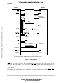
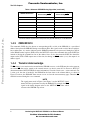
Freescale Semiconductor
Application Note
AN2247/D
Rev. 0, 1/2002
Freescale Semiconductor, Inc...
Interfacing the MCF5307
SDRAMC to an External
Master
Melissa Hunter
TECD Applications
This application note discusses the issues involved in designing external logic that allows the
ColdFire® processor’s on-chip SDRAM controller to work with external masters. Although
this document specifically refers to the MCF5307, it can be used to design an external
master-to-SDRAMC interface for the MCF5407 as well, since the SDRAMC modules are the
same.
This document assumes familiarity with the MCF5307 SDRAMC and working knowledge of
the initialization sequence required for proper SDRAM operation. For the purposes of this
application note, it is assumed that all SDRAM accesses are aligned and non-bursting. Refer
to the MCF5307 User’s Manual (MCF5307UM/D) and Using the SDRAM Controller on the
MCF5307 ColdFire Integrated Processor Application Note (AN1766/D) for more
information.
1.1
Overview
The block diagram in Figure 1 shows the connections between the MCF5307, PLD, SDRAM,
and the external master.
© Freescale Semiconductor, Inc., 2004. All rights reserved.
For More Information On This Product,
Go to: www.freescale.com
Freescale Semiconductor, Inc.
Overview
MCF5307
SDRAM
SRAS
RAS
SCAS
CAS
DRAMW
WE
SCKE
(muxed)
(linear)
Address1
CMD/AP/A10
PLD
Freescale Semiconductor, Inc...
CLK
BCLKO
TA
CLK
Address1
Address1
TS or AS
TS or AS
R/W
SIZ[1:0]
R/W
SIZ[1:0]
BG
BG
BD
BD
BR
BR
Vcc
Data[31:0]
CKE
Data[31:0]
External Master
Data[31:0]
1
RAS[1:0]
CS
CAS[3:0]
DQM
For this implementation, the MCF5307 and external master output a
linear address, while the PLD outputs a muxed address to the SDRAM.
Figure 1. Block Diagram
Once the external master is granted control of the bus, it initiates an SDRAM access by asserting either TS
or AS (only one signal can be used). The external master also needs to drive the linear address, data (if a
write cycle), SIZ[1:0], and R/W. Once the assertion of TS or AS alerts the MCF5307 to the beginning of a
new bus cycle, the processor latches the address, SIZ[1:0], and R/W signals to determine what type of bus
cycle is starting.
If the address hits in SDRAM space, the MCF5307 drives the SDRAM control signals (SRAS, SCAS,
DRAMW, SCKE (CMD), RAS, and CAS).
2
Interfacing the MCF5307 SDRAMC to an External Master
For More Information On This Product,
Go to: www.freescale.com
Freescale Semiconductor, Inc.
SDRAM Overview
The PLD’s primary responsibility is to detect SDRAM bus cycles and generate the correct muxed address
to the SDRAM. This means that the PLD needs to distinguish between an SDRAM access and an SDRAM
command, such as a refresh cycle. During read or write accesses the PLD needs to handle address muxing
and TA generation, but during other SDRAM commands the PLD should just pass the SDRAM control
signals generated by the MCF5307 through to the SDRAM.
1.2
SDRAM Overview
Freescale Semiconductor, Inc...
One of the main differences between synchronous and asynchronous DRAM is the use of commands to
control the memory’s state machine. During every clock cycle, the SDRAM latches in a new command
based on the encoding of the address and control lines. Table 1 lists all of the SDRAM commands that are
used by the MCF5307 SDRAM controller and the encoding of the ColdFire SDRAM control signals for the
associated command.
.
Table 1. SDRAM Commands Truth Table
Command
Description
RAS
SRAS
SCAS
R/W
SCKE
(CMD)
ACTV
Decode row address
L1
L
H2
H
V3
MRS
Mode register set
L
L
L
L
L
NOP
No operation
L
H
H
H
X4
PALL
Precharge all
L
L
H
L
H
READ
Read access
L
H
L
H
L
REF
Auto refresh
L
L
L
H
X
WRITE
Write access
L
H
L
L
L
1
L = Low
H = High
3 V = Valid
4 X = Don’t care
2
1.3
MCF5307 Signals
Table 2 describes the MCF5307 signals used to interface to the SDRAM and external master.
Table 2. MCF5307 Signals
Signal Name
Signal Description
SDRAMC Signals
SRAS
Synchronous row address strobe. Indicates a valid row address can be latched by the SDRAM.
Connects to SDRAM RAS input.
SCAS
Synchronous column address strobe. Indicates a valid column address can be latched by the
SDRAM. Connects to SDRAM CAS input.
DRAMW
DRAM write. Indicates direction of data transfer for SDRAM cycles:
• High indicates a read
• Low indicates a write
SCKE
Synchronous clock enable. Enables SDRAM’s self-refresh mode. When external multiplexing is
used, DCR[COC] allows the SCKE signal to provide command bit data for the SDRAM.
Interfacing the MCF5307 SDRAMC to an External Master
For More Information On This Product,
Go to: www.freescale.com
Freescale Semiconductor, Inc.
The PLD Outputs
Table 2. MCF5307 Signals (continued)
Signal Name
Signal Description
RAS[1:0]
Row address strobe. Used to select one of the two possible blocks of SDRAM that can be connected
to the MCF5307. The RAS signals should be connected to the chip select input of the SDRAM.
CAS[3:0]
Column address strobe. For SDRAM, the CAS signals function as byte enables. They should be
connected to the DQM pins of the SDRAM.
Bus Signals
BCLKO
Bus clock output. System bus clock output from the MCF5307.
Freescale Semiconductor, Inc...
Address[31:0] 32-bit address bus.
Data[31:0]
32-bit data bus.
TS or AS
Transfer start or address strobe. During external master bus cycles one of these signals must be
asserted to alert the MCF5307 to the start of a new bus cycle.
R/W
Read/write. Indicates direction of data transfer:
• High indicates a read
• Low indicates a write
SIZ
Size. Encoded signals that indicate longword, byte, word, or line transfer.
Bus Arbitration Signals
BG
Bus grant. Input to MCF5307 asserted to indicate that the MCF5307 can take mastership of the bus.
BD
Bus driven. Output from MCF5307 indicating that it is the current bus master and is driving the bus.
BR
Bus request. Output from MCF5307 to external master or arbiter to indicate that the MCF5307
requests bus mastership for one or more bus cycles.
1.4
The PLD Outputs
This section discusses each of the PLD outputs and explains how they are generated.
1.4.1
RAS, CAS, and WE
These signals are duplicates of the SRAS, SCAS, and DRAMW signals output by the MCF5307. The only
difference between the outputs of the PLD and the MCF5307 is that the PLD adds additional delay on the
signals. Care should be taken to ensure that this additional delay will not cause any timing conflicts. The
EDGESEL module can help compensate for the additional delay on the control signals; see Section 11.4.2,
“Using Edge Select (EDGESEL),” in the MCF5307 User’s Manual for more information.
1.4.2
Address
The primary function of the PLD is to generate the muxed row and column addresses for the SDRAM. The
SDRAM uses a two-phase address (a row and a column address) to access a single memory location. The
row address is latched during an ACTV command, and the column address is latched during READ or WRITE
commands (see Table 1 on page 3). Each is latched by the SDRAM during the appropriate address strobe
(SRAS and SCAS). Any method can be used to generate the muxing solution, including the muxing
algorithm already implemented by the MCF5307 SDRAMC.
4
Interfacing the MCF5307 SDRAMC to an External Master
For More Information On This Product,
Go to: www.freescale.com
Freescale Semiconductor, Inc.
1.4.2.1
The PLD Outputs
Muxing Example 1
In some cases it might be easiest to implement the same muxing scheme as used when the MCF5307 is
handling the address muxing. For more information, refer to the address multiplexing tables in Section
11.4.4.1, “Address Multiplexing,” in the MCF5307 User’s Manual.
For example, use the muxing shown in Table 3 when connecting to a 16-bit wide SDRAM port with 9
column addresses, 11 row addresses, and 2 bank selects.
Freescale Semiconductor, Inc...
Table 3. ColdFire SDRAM Muxing Algorithm Example
1
1.4.2.2
SDRAM Address Pin
Linear Address Signal
Driven during SRAS 1
Linear Address Signal
Driven during SCAS1
A0
A16
A1
A1
A15
A2
A2
A14
A3
A3
A13
A4
A4
A12
A5
A5
A11
A6
A6
A10
A7
A7
A9
A8
A8
A18
A17
A9
A20
A19
A10
A21
SCKE (CMD)
A11
A22
—
BA0
A23
—
BA1
A24
—
The linear address signals listed correspond to the physical address pin on the MCF5307.
Muxing Example 2
Using external logic to handle the address line muxing for all SDRAM bus cycles allows for any valid
muxing scheme to be used. Since the muxing scheme used by the SDRAMC is somewhat complicated, a
simpler muxing algorithm, such as that shown in Table 4, can be used instead.
Table 4. Alternate SDRAM Muxing Algorithm
SDRAM Address Pin
Linear Address Signal
Driven during SRAS 1
Linear Address Signal
Driven during SCAS1
A0
A1
A13
A1
A2
A14
A2
A3
A15
A3
A4
A16
A4
A5
A17
A5
A6
A18
Interfacing the MCF5307 SDRAMC to an External Master
For More Information On This Product,
Go to: www.freescale.com
Freescale Semiconductor, Inc.
The PLD Outputs
Freescale Semiconductor, Inc...
Table 4. Alternate SDRAM Muxing Algorithm (continued)
1
1.4.3
SDRAM Address Pin
Linear Address Signal
Driven during SRAS 1
Linear Address Signal
Driven during SCAS1
A6
A7
A19
A7
A8
A20
A8
A9
A21
A9
A10
A22
A10
A11
SCKE
A11
A12
—
BA0
A23
—
BA1
A24
—
The linear address signals listed correspond to the physical address pin on the MCF5307.
CMD/AP/A10
The command (CMD) bit (also known as auto-precharge(AP) or A10 of the SDRAM) is a specialized
address line input to the SDRAM. During a row address phase, this signal is used as a bit in the row address,
but, at other times, it is used to indicate specific SDRAM commands to be processed. Setting the COC bit
in the DRAM control register (DCR) allows the MCF5307 to drive the command data on the SCKE line
instead of driving the command on one of the address lines. So, the data from the SCKE line should be
output on the PLD’s CMD output most of the time, but during an SRAS strobe (ACTV) the output is an
address signal.
1.4.4
Transfer Acknowledge
The TA timing is not consistent for external master SDRAM accesses, so the PLD must be used to generate
an external TA that can be routed to the external master (see device errata #23 in Errata to MCF5307
(document number: MCF5307ER/D) for more information). Consider 2 basic cases—writes and reads. For
a write cycle, the data is latched by the SDRAM at the same time as the column address, as shown in
Figure 2; however, the SDRAMC must execute a PALL to close the current memory page. Therefore, TA
should be asserted during the PALL command.
NOTE
The signal names used in Figure 2 and Figure 3 are the MCF5307 signal
names NOT the signal names used by the SDRAM. For example, the RAS
signal in the timing diagram refers to the MCF5307 RAS lines which
connect to the SDRAM chip selects.
6
Interfacing the MCF5307 SDRAMC to an External Master
For More Information On This Product,
Go to: www.freescale.com
Freescale Semiconductor, Inc.
The PLD Outputs
Bus Cycle Terminated
during PALL Command
SDRAM Latches Data
BCLKO
TS
Address
Freescale Semiconductor, Inc...
Data
SRAS
SCAS
DRAMW
RAS
CAS
TA
ACTV
NOP
WRITE
NOP
PALL
Figure 2. SDRAM Write Cycle Termination Timing
During read cycles there is a delay between when the column address is latched and when the data becomes
available known as CAS latency (given in bus clocks). So for read cycles, once the PLD detects the end of
the column address phase, it then needs to wait the same number of clocks as the CAS latency before
terminating the bus cycle as shown in Figure 3.
Interfacing the MCF5307 SDRAMC to an External Master
For More Information On This Product,
Go to: www.freescale.com
Freescale Semiconductor, Inc.
The PLD Outputs
Data Latched by
SDRAM and Bus
Cycle Terminated
BCLKO
TS
Address
Freescale Semiconductor, Inc...
Data
SRAS
SCAS
DRAMW
RAS
CAS
TA
ACTV
NOP
READ
NOP
PALL
Figure 3. SDRAM Read Cycle Termination Timing
1.4.5
PLD Operation during SDRAM Commands
During all commands, the PLD should drive the SRAS, SCAS, and DRAMW on the RAS, CAS, and WE
outputs of the PLD. Table 5 describes the effect of each SDRAM command on PLD operation.
8
Interfacing the MCF5307 SDRAMC to an External Master
For More Information On This Product,
Go to: www.freescale.com
Freescale Semiconductor, Inc.
Programming the MCF5307 SDRAMC
Table 5. PLD Operation During SDRAM Commands
Freescale Semiconductor, Inc...
Command
1.5
PLD Operation
ACTV
Row address strobe and bank activation. During the ACTV command the
SDRAM latches the row address. The PLD should drive the row address for
the selected muxing algorithm.
MRS
Mode register set command. Sets the mode register physically located on the
SDRAM chip(s). The mode register controls some of the timing and mode
options for the SDRAM including the CAS latency. This command is unique in
that the data written to the mode register is latched from the address lines.
This means that the data to be written to the mode register must be mapped
onto the address lines. Refer to Section 11.5.5, “Mode Register Initialization,”
in the MCF5307 User’s Manual for an example on how to determine the
correct address to use during the mode register set command.
NOP
No operation. The PLD does not need to do anything.
PALL
Precharge all. Closes the current SDRAM page, so next access starts with an
ACTV command. PLD needs to drive command data from the SCKE line onto
A10 of the SDRAM.
READ
Read. The column address to be read is latched by SDRAM. PLD should drive
the column address for the selected muxing algorithm and drive command
data from SCKE line onto the SDRAM’s CMD pin. The READ command should
also start the PLD counter responsible for generating the TA.
REF
Refresh. Periodic refresh is required to retain data stored in SDRAM. PLD
should pass through SDRAM control signals.
Programming the MCF5307 SDRAMC
This application note is not intended to address the settings and procedures for programming the SDRAMC;
however, it is useful to note that the DRAM control register (DCR) should be configured with the no address
multiplexing (NAM) and command-on-SDRAM clock enable (COC) bits both set. The NAM bit turns off
the MCF5307’s internal muxing capability so that all address muxing is handled by the PLD. The COC bit
enables the SDRAMC to place the command bit information for the SDRAM on the SCKE line. The PLD
drives the command data from SCKE onto the SDRAM’s A10 address line. Since the SCKE signal is used
to provide the SDRAM’s command bit data, the self-refresh low-power mode is not available with this
implementation. The CKE signal on the SDRAM should be tied high to disable the self-refresh mode.
For more information on initializing the SDRAM see the SDRAM section of the MCF5307 User’s Manual.
Interfacing the MCF5307 SDRAMC to an External Master
For More Information On This Product,
Go to: www.freescale.com
Freescale Semiconductor, Inc.
Freescale Semiconductor, Inc...
Programming the MCF5307 SDRAMC
10
Interfacing the MCF5307 SDRAMC to an External Master
For More Information On This Product,
Go to: www.freescale.com
Freescale Semiconductor, Inc.
Freescale Semiconductor, Inc...
Programming the MCF5307 SDRAMC
Interfacing the MCF5307 SDRAMC to an External Master
For More Information On This Product,
Go to: www.freescale.com
Freescale Semiconductor, Inc...
Freescale Semiconductor, Inc.
Home Page:
www.freescale.com
email:
[email protected]
USA/Europe or Locations Not Listed:
Freescale Semiconductor
Technical Information Center, CH370
1300 N. Alma School Road
Chandler, Arizona 85224
(800) 521-6274
480-768-2130
[email protected]
Europe, Middle East, and Africa:
Freescale Halbleiter Deutschland GmbH
Technical Information Center
Schatzbogen 7
81829 Muenchen, Germany
+44 1296 380 456 (English)
+46 8 52200080 (English)
+49 89 92103 559 (German)
+33 1 69 35 48 48 (French)
[email protected]
Japan:
Freescale Semiconductor Japan Ltd.
Headquarters
ARCO Tower 15F
1-8-1, Shimo-Meguro, Meguro-ku
Tokyo 153-0064, Japan
0120 191014
+81 2666 8080
[email protected]
Asia/Pacific:
Freescale Semiconductor Hong Kong Ltd.
Technical Information Center
2 Dai King Street
Tai Po Industrial Estate,
Tai Po, N.T., Hong Kong
+800 2666 8080
[email protected]
For Literature Requests Only:
Freescale Semiconductor
Literature Distribution Center
P.O. Box 5405
Denver, Colorado 80217
(800) 441-2447
303-675-2140
Fax: 303-675-2150
LDCForFreescaleSemiconductor
@hibbertgroup.com
Information in this document is provided solely to enable system and software
implementers to use Freescale Semiconductor products. There are no express or
implied copyright licenses granted hereunder to design or fabricate any integrated
circuits or integrated circuits based on the information in this document.
Freescale Semiconductor reserves the right to make changes without further notice to
any products herein. Freescale Semiconductor makes no warranty, representation or
guarantee regarding the suitability of its products for any particular purpose, nor does
Freescale Semiconductor assume any liability arising out of the application or use of
any product or circuit, and specifically disclaims any and all liability, including without
limitation consequential or incidental damages. “Typical” parameters which may be
provided in Freescale Semiconductor data sheets and/or specifications can and do
vary in different applications and actual performance may vary over time. All operating
parameters, including “Typicals” must be validated for each customer application by
customer’s technical experts. Freescale Semiconductor does not convey any license
under its patent rights nor the rights of others. Freescale Semiconductor products are
not designed, intended, or authorized for use as components in systems intended for
surgical implant into the body, or other applications intended to support or sustain life,
or for any other application in which the failure of the Freescale Semiconductor product
could create a situation where personal injury or death may occur. Should Buyer
purchase or use Freescale Semiconductor products for any such unintended or
unauthorized application, Buyer shall indemnify and hold Freescale Semiconductor
and its officers, employees, subsidiaries, affiliates, and distributors harmless against all
claims, costs, damages, and expenses, and reasonable attorney fees arising out of,
directly or indirectly, any claim of personal injury or death associated with such
unintended or unauthorized use, even if such claim alleges that Freescale
Semiconductor was negligent regarding the design or manufacture of the part.
AN2247/D
For More Information On This Product,
Go to: www.freescale.com