1
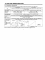
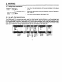
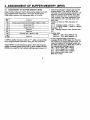
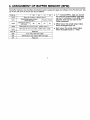
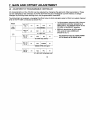
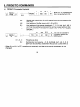
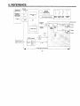
ADVANCED AND EVER ADVANCING
MITSUBISHI ELECTRIC
PROGRAMMABLE CONTROLLERS
SER'S MANUAL
r
-
%
..
5."
*+*%
8
s
..-... -..---
.*"
"
'
.-., ,
y....r.
"...."lit"
u
t
:"3
~ f . ~ u l l w a lJeLLlIlgs
G
by the TO instruction of the base unit.
sion unit.
1
Gain and offset can be adjusted using the procedure described on pages 13 ro 15.
Foreword
This manual provides technical information on the use
of the FX-2DA Analog Output Block in connection with
the FX programmable controller.
Users should ensure that the details of this manual are
studied and understood before attempting to install or
use these units.
CONTENTS
1. INTRODUCTION
2. OUTLINE SPECIFICATION
3. WIRING
4. ASSIGNMENT OF BUFFER MEMORY (BFM)
5. STATUS INFORMATION
6. EXAMPLE PROGRAMS
7. GAIN AND OFFSET ADJUSTMENT
8. FROMITO COMMANDS
9. REFERENCE
10. APPENDIX
1. INTRODUCTION
The FX-2DA analog output unit receives up to 2 channels of 12-bit digital data stored in 16-bit words
from an FX series programmable controller and converts it into 2 channels of analog output (either
voltage or current). Optical coupling is used to ensure that voltage surges do not damage other parts
of your equipment.
(1) Compatible Programmable Controllers
The FROM-TO command is used for
transferring data tolfrom the prograrnmable controller, so versions 2.0 or subsequent versions of the FX series
programmable controllers (those with
serial no. 13XXXX or larger) are required.
(3)
Analog Output Range
The preset ranges -10V to + 10V and
+4mA to +20mA can be selected individually for each channel. Current or
voltage selection is made by buffer mernory assignment and terminal wiring.
(4)
Gain and Offset
(2) Configuration Specifications
The FX-2DA occupies 8 110 points but
does not affect the addressing of normal input and output relays. It is important only when maximum I10 is
considered. The FX-2DA draws 30mA
from the 5V rail from the base or extension unit.
Gain and offset can be adjusted by the
user to give the desired output range.
The desired range must be within the
convertable maximum of the unit.
Adjustment can be made by the front
panel switches or by software settings
by the TO instruction of the base unit.
2. OUTLINE SPECIFICATION
(1)
Dimension mm (inch)
Weight: Approx. 0.5 kg (1.1 Ibs.)
Accessories: Self- adhesive labels for special block
number identification
2. OUTLINE SPECIFICATION
(2) Perfomance Specifications
The environmental specifications for the FX-2DA are the same as those for your base unit.
Gain and offset can be adjusted using the procedure described on pages 13 to 15.
9
3. WIRING
Programmable
controller
Extension cable
*2
*I Use a twisted pair shielded cable for the analog *4 Connect the ground terminal on the FX-2DA
output. This cable should be wired away from
with the ground terminal on the base unit of the
power lines or any other lines which could inprogrammable controller. Use class 3 groundduce noise.
ing on the base unit, if available.
* 2 Apply 1-point grounding at the load side of the Caution:
output cable (class 3 grounding: 100Q or less).
l
drive current
If electrical noise is caused from grounding, dis- (a) 'l%esame output ~ h a n n ecannot
and voltage output loads at the same time!
connect from ground.
*3 If electrical noise or a voltage ripple exists at the (b) Shorting the voltage output terminals may damage the unit!
output, connect a smoothing capacitor of 0.1
to 0.47,uF, 25V.
3. WIRING
(1)
Using crimp terminations
* Use only crimp terminations of the type indicated in the figure
6.8(0.27")
or less
at left.
For M3.5(0.14in.)
and 8kg.cm.
1
6.8(0-27'''
or less
(2)
* Secure the termination using a tightening torque of between 5
* Only use the terminations indicated at left.
Use with other special blocks
The FROM and TO commands are also used by other Special Function Blocks, (e.g. the analog input
blocks, high-speed counter blocks, pulse output blocks, etc.). These may be connected directly t o the
FX Programmable Controller's extension port or to any other extension unit's right side extension port.
Each special unit or block is consecutively numbered from 0 to 7 beginning from the one closest to the
base unit. A maximum of eight special blocks can be connected to one base unit.
FX-48MR
XO-X27
YO-Y27
FX-4AD
Special
block
No.0
FX8EX
X30X37
FX-2DA
Special
block
No.1
FX-32ER
X40-X57
Y30-Y47
FX-PAD-PT
Specla1 block
No.2
ASSIGNMENT OF BLlFFER MEMORY (BFM)
Data transfer between the FX-2DA analog output "nit and
the programmable controller is through the FX-2DA's
RAM buffer memory (32 addresses each of 16 bits).
(1)
. .
BFM
Contents
NO.
#O
Analog output mode (currentlvoltage) default = (HOO)
* #I
Output data CHI
'f2
Output data CH2
#3
Reserved
-
#4
:
* #5
*#6
to #lQ
Reserved
last data reset default = HOO
Reserved
In BFM's (buffer memory) with an "*", data can be written
from programmable controller using the TO command.
These BFM's should always be given when the programmable controller goes from STOP to RUN. Buffer memory
(BFMs) are reset t o their default settings upon power on.
1. Switching between voltage and current
Output modes. The value-0fBFM #O
switches the analog output between voltage and current on channels CHI and
CH2. It takes the form of a 2-character
HEX number. The least significant character controls CHI and the other controls CH2.
Control of each 0 HEX character of
HOO:
0 = 0 : Voltage output (-10V to + 10V)
0 = 1 : Current output ( + 4mA to + 20mA)
Example : H I 0
CHI : Voltage output, CH2: Current output
2. Output data:
BFM #1 : CHI data (default =0)
BFM #2 : CH2 data (default = 0)
3. If the programmable controller is
changed to the STOP state, the FX-2DA
will continue t o output the last value. To
reset the output to the offset value, set
the HEX characters of BFM #5 to one of
the appropriate settings below:
H01 : CH2 = Hold, CHI =Reset
H I 0 : CH2 = Reset, CHI = Hold
H11 : CH2 = Reset, CHI = Reset
Both channels are held when
BFM #5 = HOO.
4. ASSIGNMENT OF BUFFER MEMORY (BFM)
The buffer memory also handles information used to adjust the gain and offsets of the FX-2DA unit. Status of the unit such as errors are also available.
In "*" marked BFM's, data can be written from the programmable controller
via the TO command. From BFM #29
and #30, data can be read via the
FROM command.
a Offset value: the actual output value
when the digital input is 0.
a Gain value: the actual output value
when the digital input is
+ 1000.
4. ASSIGNMENT OF BUFFER MEMORY (BFM)
1. When BFM #20 is set to K1, all settings in the
buffer memory are reset to their default settings. This allows the buffer memory settings
to be set from the beginnivg again when many
settings have been corrupted.
2. If (b1,bO) of BFM #21 is set to (1,0), gain and
offset adjustments are prohibited. This is to
prevent inadvertent misuse by the operator. To
adjust the gain and offset, (b1,bO) of BFM #21
must have the values (0,l). The default is set
at (0,l).
3. Each time a TO instruction is used to send
data to BFM #22 (gainloffset setting command), the designated gain and offsets of
each channel (G202 G101) are adjusted with
the values in BFM #23 and #24. This action
causes the adjustments t o be written to internal non-volatile EEPROM memory. Limit this
action to as little as possible to preserve the
life of the EEPROM memory.
4. Gain and offset values in BFM #23 and #24
are set in units of mV or PA.
Due to the resolution of the unit, the actual re
sponse will be in steps of 5mV or 20pA.
Caution
Because of the time taken to wriie to the EEPROM memory, a delay of 300ms is needed between
instructions that cause a write to the EEPROM.
Therefore, a delay timer should be used before further writes to the EEPROM, after executing the
following:
Writing to BFM #0, #5 or #21.
The gainloffset command with BFM #22.
The default command with BFM #20.
5. STATUS INFORMATION
(1)
Status information BFM #29
(2)
Model code number BFM #30
The ldentification code for a Special Block is
read using the FROM command.
The ldentification code for the FX-2AD unit is
K3010.
The programmable controller can use this facility in the program to identify the special
block before commencing any data transfer
from and to the special block.
Caution
adjust prohibit
BFMXPl is Set
at (0,l)
Bits b5 to b7,b9, b l 1, and b13 are undefined.
Values of BFM #0, #5, #23 and #24 are copied
to EEPROM memory of the FX-2DA. BFM #21
and #22 are only copied when data is sent to
gainloffset command BFM #22. BFM #20 also
writes to the EEPROM memory.
The EEPROM has a life of about 10,000 cycles
(changes), so please do not use programs which
frequently change these BFMs.
Example #1
If the gain and offset settings are left at their default values, and the status information is ignored, you
can use the simple program which follows.
KO
1
pulse
Block No.
No.1
HID
I
I
BFM
#O
Voltage output on both CHI and CH2
KI
J
I
Transfer Number of
data HlO words
W~hdpAUdt~bCHlirtolhrdda~W.
WnbIlma~'qut~lo~Molhrbta~D1.
K1
DO
K2
Range: -2048 to +2047
(DO) BFM #1 (Output to CHI)
(Dl) BFM #2 (Output to CH2)
monltor
Procedure
1. Write the program into the programmable controller.
2. Connect the FX-2DA unit to the base unit of the programmable controller as the 2nd special block.
3. Set the MODE switch on the FX-2DA panel to READY.
4. Turn on the programmable controller and the FX-2DA unit.
Result :
When the programmable controller is in RUN mode, the voltage output on channels CHI and CH2 will
vary according to the digital values in data registers DO and D l . When the programmable controller is in
STOP mode the last output made during RUN mode will be maintained.
In the above program the FX-2DA unit occupies the position of special block No.1 (that is the 2nd closest
special block to the base unit). Voltage output from -10V to + 10V is produced from channel CHI and
+ 4mA to + 20mA from CH2.
6. EXAMPLE PROGRAMS
Example #2
In the following example, channel CHI is set to voltage output, while CH2 is set to current output. The
FX-2DA unit is connected at the position of special block No.1. If the programmable controller is
changed to the STOP mode, the last data sent will remain and the outputs will hold.
FNC 78
FROM
1 monitor
K,
U30
02
K1
1
Block No. 1, BFM #30 (Identification code)
Transfer to D2.
When Identification code is K3010 (FX9DA),
M I becomes ON.
FNC 7s
TO
K1
KO
nr D
KI
Block
No.1
BFM XO
Transfer
data H I 0
Number of
words
HlO+unit No. 1 BFM #O
CHI: voltage output, CH2: current output
(DO)+BFM #1 (output to CHI)
(Dl)-*BFM #2 (output to CH2)
BFM #29 (b15 to bO)+(M25 to M10)
Reads the status information.
... .
-
IY
Al
No error
A+, , I
-
'READY' O u t ~ u tranae
normal
Output data normal
6. EXAMPLE PROGRAMS
(1)
Operation
(2)
Abnormality check
extended cable for the FX-2DA are properly
connected.
The following can be checked with LEDs located
on the main panel of the FX-2DA.
POWER LED
2) 5V, 30mA is supplied from the base and extension units for the FX-2DA. Check that power
overload is not caused by this or any other
special block.
Lights up when 5V power is supplied from
the programmable controller. If not, check if
the extension cable is properly connected.
24V LED
3) When DC 24V power is supplied from the
Lights up when DC 24V power is supplied to
the terminal of the FX-2DA. If DC 24V +/10% is supplied but this does not light up,
failure may have occurred on the base unit.
D-A LED
1) Check if the output wiring, power wiring, and
base and extension units of the programmable controller, check that the current is below
the allowable service current on the programmable controller side (varies according to the
number of extension blocks connected).
4) Set the MODE switch on the FX-2DA to the
"READY" position, and turn the DC 24V power
on.
5) Turn the programmable controller and RUN
input ON. However, output mode of BFM #O
should be set in advance depending on voltagelcurrent output.
Lights up when Digital to Analog conversion
is executing normally. It goes off if b l to b4
of buffer memory #29 is generated ON for all
the channels.
7. GAIN AND OFFSET ADJUSTMENT
(1)
Standard characteristics of voltage output
I
+ 10.235
+'OV"
Analog output
-
Ga~n
-10.24V
(2)
/
.,--------
Digital output
+ 2047
-
Standard characteristics of current output
I
Analog
output
Offset
The solid lines show the I10 characteristics when
the gain and offsets are left at their default settings. The dashed lines show examples of adjustments to the gain and offsets. Voltage or current
output selection is set through the output wiring,
and by a command from the programmable controller.
Gain and offset settings will remain even after
power OFF.
Offset value:
the analog output when the
digital input is 0.
Gain value:
the analog output when digital input is + 1000.
When the gain value is small (implying a steep
slope), a small change in analog input will produce a large change in digital output.
\
+4mA
.'
0
,-
o
Digital output
-
1-
+ 1000
When the gain value is large (implying a gentle
slope), a large change in analog input will only
produce a small change in digital output.
7. GAlN AND OFFSET ADJUSTMENT
(3)
Gain and Offset Adjustment Using Switches on the FX-2DA Unit
The gain and offsets can be adjusted by using
the switches on the FX-2DA panel with the aid of
a voltmeter and an ammeter which are to be connected to the FX-2DA. With these procedures you
still need to set the input mode BFM #O.
5
Press the OFFSET button once with a ball
point pen. The D-A LED lights up. The present offset value (voltage or current) is output.
Use the UP,DOWN switch to reach the
desired OFFSET value. (ranae:
-5V to + 5V
.
or -20mA to +20mA)
w
After (bl, bO) of BFM #21 is changed to (1,0), you
Can no longer change the gainloffsets'
therefore write (0,1) to ( b l ,bO) of BFM #21 prior to
adjusting the gainloffset settings. (Note: (0.1) is the
default value)
1 Turn on DC 24V power of the FX-2DA. The
24V LED lights up.
2
3
4
7
Press the GAIN button once with a ball point
pen. The offset value is read and the
value is output.
8
Use the UPIDOWN switch to reach the
desired GAlN value.
range:
Gain value - offset value
= 1V to 15V (voltage output)
= 4mA to 32mA (current output)
Turn on the FX series programmable controller connected with the FX-2DA. The POWER
LED lights up. (The programmable controller
should be in STOP mode.)
9
Connect the load and voltmeter or ammeter
to the CHI terminal. (between V+ and V- terminals for voltage output, and between I +
and I-terminals for current output)
10 Repeat steps 3 to 9 for CH2 (if desired), then
set the MODE switch to READY. Adjustment
Set the MODE switch to CHI.
. ~ ~ -
Set the MODE switch
to the READY ~osition.
~.
The gain value is read, the^-A LED goes off,
and the offset value is output.
~
is completed.
7. GAIN AND OFFSET ADJUSTMENT
(4)
ADJUSTMENT BY PROGRAMMABLE CONTROLLER
I10 characteristics of the FX-2DA can be adjusted by changing the gain and offset parameters. 'These
can be changed by the switches of the FX-2DA with the aid of Voltage & Current meters or simply
changed by writting these settings from the programmable controller.
The following is an example, changing the offset value to OmA and gain value to 20mA on output channel
CH2 of the FX-2DA connected as block No.1.
In the program shown at left, the programmable controller should be in
RUN status, and MODE switch of the
FX-2DA in the READY position.
BFM #O should be of HEX value
H10, and (b1,bO) of BFM #21
should be (0,l).
HlO-BFM#O
Pulse
TO
Kl+BFM X21
FNC79
K23
K1
KO
This statement may be omitted BFM
-'#23
is already at its defautt value.
if
K1
KO- BFM #23 (offset)
I
I
I
. .
I
I
I
I
K20000- BFM Y 24 (gain)
FNC79
TO (PI
K1
K22
HC
K1
HC+BFM X22 (offsetlgain set)
8. FROMITO COMMANDS
(4)
FROMITO Commands Explained
FROM
m l:
rn2:
[D .] :
n:
ml
m2
[D.]
n
K1
K30
DO
K1
Special unit or block No. (KO to K7 starting from the one closest to the
base unit)
Head address of buffer memory (n2 = KO to K31)
Head address of the transfer destination. T, C, D, KnM, KnY, KnS, V
and Z can be specified and element No. can be coupled with an index.
Number of transfer points (K1 to K32 but K1 to K16 for DFROM,
DFROMP.)
ml
-
rnl ,m2 ,n:
.
BFM #30 in special block
No.0 is transferred to DO.
TO
KI
m2
[S']
D2
n _ D3, D2 are transferred
to special block No.1
t~
BFM #2, #l.
The same as above
Head device no. of source. T, C, D, KnX, KnM, KnY, YnS, V, 2,K,
[S.]:
and H can be specified, and element No. can be coupled with an
index.
When XI0 or X I 1 is OFF, transfer is not executed, and data at the transfer destination is not
changed.
9. REFERENCE
-
5~ bower
1
Command in-
formation
EEPROM
memory for
offset and gain 3
,
Buffer Memory
Itatus read
~nputparameter settings
I
I
I
FX ~erles
FROM
I
CPU
FX-2DA Analog Oulput Block
17
7 3
MODE OFF-SET QA'N
witch ~ w i l c h cwltch
UPIDOWN
&tch
10. APPENDIX
ATTENTION FOR WHEN SWITCHING SYSTEM ON/OFF
Due to the inevitable timing difference of the DC24v for the analog circuits and other power lines
of the base unit, the output of the analog output Mock may behave erroneously before settling
down to operational conditions in approximately 1sec. Therefore, ensure that this behavior is
taken into account such that the end performance of the system is not degraded.
power switch
(example)
cut analog lines
before switching
- r--1
DC24V
supply
FX-2DA
-Analog output block
-1
I
I
I
I
L - - A
External analog
machine
MEMO
Revisions
EDITION DATE
Jun. 1991
Aug. 1991
Nov. 1992
MANUAL NUMBER
REVISION
JY992D28301 A
First edition
JY992D28301 B
P.18 "ATTENTION FOR WHEN SWITCHING SYSTEM ON I OFF" added.
JY992D28301 C
Diagram corrections : Page 4
Text corrections
: Pages 6,9,14
EEPROM CAUTION : Page 8
Under no circumstances will Mitsubishi Electric be liable or responsible for any
consequential damage that may arise as a result of the installation or use of this
equipment.
All examples and diagrams shown in this manual are intended only as an aid to understanding the text, not to guarantee operation. Mitsubishi Electric will accept no
responsibility for actual use of the product based on these illustrative examples.
Owing to the very great variety in possible applications of this equipment, you
must satisfy yourself as to its suitability for your specific application.
A MITSUBISHI ELECTRIC CORPORATION
HEAD OFME: MITSUBISHI DENKI BUXj MARUNOWHI TOKYO 100 TELEX: J24532 CABLE MELCO TOKYO
HlMEJl WORKS: 840. CHIVODA CHO. HIMEJI. JAPAN
JY992D28301C
HI-IB-059-C (9211) (SEN) @
Effective NOV. 1992
Specifications are subject
to change without notice.