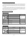
1
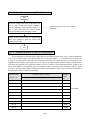
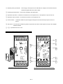
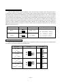
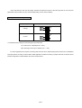
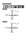
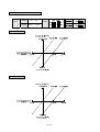
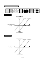
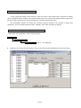
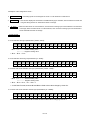
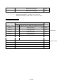
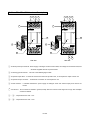
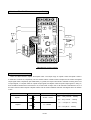
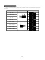
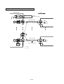
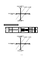
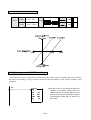
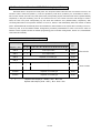
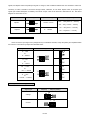
Chapter 18
AIO Module
18.1 FBs-6AD Analog Input Module
FBs-6AD is one of the analog input modules of FATEK FBs series PLC. It provides 6 channels A/D input with 12
or 14 bits effective resolution.. Base on the different jumper settings it can measure the varieties of current or voltage
signal. The reading value is represented by a 14-bit value no matter the effective resolution is set to 12 or 14 bits. In
order to filter out the field noise imposed on the signal, it also provides the average of sample input function.
18.1.1 Specifications of FBs-6AD
Item
Specifications
Total Channel
6 Channel
Digital Input Value
Span
Of
Analog
input
Bipolar*
Unipolar
Remark
−8192~+8191 or
0~16383(14 bits)
−2048~+2047 or
0~4095(12 bits)
*1.Voltage:−10~10V
5.Current:−20~20mA
5V
2. Voltage:−5~5V
6. Current:−10~10mA
10V
3. Voltage:0~10V
7. Current:0~20mA
5V
4. Voltage:0~5V
8. Current:0~10mA
10V*
Resolution
Finest resolution
*: It means the default setting
14 or 12 bits
Voltage:0.3mV
= Analog input signal / 16383
Current:0.61µA
I/O Points Occupied
6 IR(Input Register)
Accuracy
Within ±1% of full scale
Conversion Time
Updated each scan
Maximum absolute input
signal
Voltage:±15V(max)
Current:±30mA(max)
Input resistance
63.2KΩ(Voltage input)、250Ω(Current input)
Isolation
Transformer(Power) and photocouple(Signal)
Indicator(s)
5V PWR LED
Supply Power
24V-15%/+20%、2VA
Internal Power Consumption
5V、100mA
Operating Temperature
0 ~ 60 ℃
Storage Temperature
-20 ~ 80 ℃
Dimensions
40(W)x90(H)x80(D) mm
18-1
It may cause the destruction to
hardware if exceeds this value.
18.1.2 The Procedure of Using FBs-6AD Module
Start
Set the I/O voltage/current (V/I), polarity (B/U), and
the V/I range of each point before installation.
Connect FBs-6AD to the expansion interface on
-------
PLC in series and connect an external 24VDC
Please refer to section 18.1.4 for hardware
explanation.
source and analog output wires to the module.
Directly read the value of the six corresponding
value input registers to obtain the analog input
reading of CH0~CH63.
End
18.1.3 Address Allocation of FBs-PLC Analog Inputs
The I/O addressing of FBs-6AD inputs is beginning from the module closest to main unit, it is orderly numbered as
CH0~CH5 (1st module), CH6~CH11 (2nd module), CH12~CH17 (3rd module)…… and increased with occurring order
number, i.e. for each module, it adds with 6 and is totally 64 inputs from CH0~CH63, and they are corresponding to the
respective internal analogue input register of PLC (so called as IR register) R3840~R3903 as listed in following table.
After connecting FBs-6AD to the expansion interface on the PLC, FBs-PLC will automatically detect the number of AD
points. WinProladder will automatically detect and calculate the IRs on the system after connecting to the PLC. Users
may refer to the I/O Module Number Configuration provided by WinProladder in order to find out the exact I/O address of
each expansion module to facilitate programming.
Numeric Input
Content of IR (CH0~CH63)
Register(IR)
B 1 5 B 1 4 B 1 3 B 1 2 B 11 B 1 0 B 9 B 8 B 7 B 6 B 5 B 4 B 3 B 2 B 1 B 0
Input label
Of FBs6AD
IR+0
14/12 bit ; 14-bit , B14~ B15= B13 ; 12-bit, B12~ B15= B11
CH0
IR +1
14/12 bit ; 14-bit , B14~ B15= B13 ; 12-bit, B12~ B15= B11
CH1
IR +2
〃
CH2
IR +3
〃
CH3
IR +4
〃
CH4
IR +5
〃
CH5
IR +6
Depends on module type
CH X
IR +7
Depends on module type
CH X
IR +8
〃
CH X
IR +9
〃
CH X
18-2
F Bs - 6 AD
〃
CH X
R3 897
〃
CH X
R3 898
〃
CH X
R3 899
〃
CH X
R3 900
〃
CH X
R3 901
〃
CH X
R3 902
Depends on module type
CH X
R3 903
Depends on module type
CH X
~~
..... .
~~
..... .
~~
....
~~
R3 896
Other Modules
18.1.4 FBs-6AD Hardware Description
1
6
8
7
※ FBs-6AD contains 3 PCBs overlapping one
another. The lowest one is the power
2
supply unit (isolated power supply). The
24V IN
V
I0+
I1+
AG
I1I0-
middle one is the I/O board (connectors
are on this layer). The upper one is the
I U B 5V 10V
control board (control/expansion I/O
connections) as described below.:
4
POW
3
FBs-6AD
I4+
I5+
I2+
I3+
I4I5I2I3-
5
9
10 11 12
Outlook of top view
18-3
1
○
External power input terminal :Power supply of analogue circuit for FBs-6AD, the voltage can be 24VDC±20% and
should be supplied with 4W of power at least.
2
○
Protecting ground terminal:Connect to the shielding of the signal cable.
3
○
Expansion input cable:It should be connected to the front expansion unit, or the expansion output of main unit.
4
○
Expansion output connector:Provides the connection for next expansion unit.
5
○
Power indicator: It indicates whether the power supply at analogue circuit and external input power source are
normal.
6
○
AG Ground:No connection is needed in general; except when the common mode signal is too high. See examples
overleaf for details.
7 ~○
12 :Input terminal of CH0~CH5.
○
18.1.4.1
FBs-6AD Hardware Jumper Setting
B
U
JP5 V
I
JP1
JP4 V
I
B
JP3
U
JP2
5V
10V
V
I
V JP7
I
JP8 V
I
V
JP6
I
JP9 V
I
Pin layout in control board (open top cover)
Pin layout on I/O board (remove control board)
18-4
1. Input code format selection (JP1)
Users can select between unipolar and bipolar codes. The input range of unipolar codes and bipolar codes is
0~16383 and –8192~8191, respectively. The two extreme values of these formats correspond to the lowest and highest
input signal values, respectively (see table below). For example, if the input signal type is set to -10V~ +10V, the unipolar
code corresponding to the input is 8192 and the bipolar code corresponding to the input is 0 for 0V input. If the input is
10V, the unipolar code corresponding to the input is 16383 and the bipolar code corresponding to the input is 8191. In
general, the input code format is selected according to the form of input signals; i.e. unipolar codes for unipolar input
signals; and bipolar codes for bipolar input signals. In doing so, their correlations will become more heuristics. Unless it is
necessary to make a deviation conversion through FUN33; otherwise, do not select bipolar codes for unipolar input
signals (see FUN33 description for details). The format of input codes of all channels is selected from JP1. See above
diagram for the location of JP1:
Input Code Format
JP1 Setting
Input Value Range
- 819 2~ 8 191
Bipolar
Corresponding Input Signals
- 1 0 V~ 10 V(- 20mA~ 20 mA)
B
Unipolar
U
- 5 V~ 5V(-20mA~ 2 0m A)
0V~ 10 V(0 m A~ 20mA)
0~ 1638 3
0V~ 5 V( 0 m A~ 10 mA)
2. Input signal form setup (JP2&JP3)
Users can set the input signal form (voltage/current) of individual channels; except the polarity and amplitude which
are common. The location of jumpers are tabulated below:
Signal Form
JP3 Setting
JP2 Setting
0~ 10V
or
0~ 20mA
0~ 5V
or
0~ 10mA
-10~ +10V
or
-20~ +20mA
5V
10V
-5~ +5V
or
-10mA~ +10mA
5V
10V
18-5
CH0~CH5 share the JP2 and JP3 jumper, therefore all channels must be of the same type that is one of the four
types listed at above table. Only the current/voltage setting can be chosen arbitrary:
3. Voltage or current setting (JP4~JP9)
Signal Type
JP4(CH0) ~ JP9(CH5) Setting
Voltage
Current
*The default factory settings of 6AD analogue input module are:
Input code format Æ Bipolar(-8192~+8191)
Input signal type and range Æ Bipolar(-10V ~ +10V)
For those applications that require the setting differ than the above default setting should make some modifications
of jumper position according to above tables. While application, besides the setting of jumper should be conducted, the AI
module configuration of WinProladder also need to be performed.
18-6
18.1.5 FBs-6AD Input Circuit Diagram
Inputs
FBs-6AD
+15V
24V+
15V
+ 24VDC
External power supply
24V
+
+
V
I0+
I
I0
V
I1+
I
I1
V
CH0
Ch0Input
Input
(Voltage sou
(Voltage Source)
I
CH1
Ch1Input
Input
(Current sou
(Current Source)
V
CH5
Ch5Input
Input
(Voltage sou
(Voltage Source)
AG
I
I5+
V
I5
+
Voltage/
Current
selection
Twisted pair with shielding
18.1.6 FBs-6AD Input Characteristics and Jumper Setting
Users can select the Input ranges of FBs-6AD from the jumpers described above, such as V/I, U/B (I/O codes), U/B
(signal form), 5V/10V, etc. The Input signals conversion characteristics of these settings are illustrated below. Users can
adjust different Input forms by coordinating the conversion curve with various V/I (voltage/current) Input settings. See
Section 18.1.4 for details of V/I settings :
18-7
Diagram 1:Bipolar 10V(20mA)Span
Input
Range
Voltage
−1 0 V~ 10 V
Current
−2 0m A~ 20 mA
Jumper
Setting
14 bit input format
12 bit input format
18-8
Diagram 2:Bipolar 5V(10mA)Span
Input
Range
Voltage
−5 V~ 5V
Current
−1 0m A~ 10 mA
Jumper
Setting
14 bit input format
12 bit input format
18-9
Diagram 3:Unipolar 10V(20mA)Span
Input
Range
Voltage
0 V~ 1 0 V
Current
0 m A~ 20 mA
Jumper
Setting
14 bit input format
12 bit input format
18-10
Diagram 4:Unipolar 5V(10mA)Span
Input
Range
Voltage
0 V~ 5 V
Current
0 m A~ 10 mA
Jumper
Setting
14 bit input format
12 bit input format
Analog Input(MAX.)
+5V(+10mA)
Input Register Value
(12 bit)
-2048
Bipolar(B)
Unipolar(U)
+2047
+4095
0
0V(0mA)
Analog Input(Min.)
1 8 - 11
18.1.7 Configuration of Analog Input
For the analog input reading of FBs series PLC, there are 3 kinds of data formats used to represent the reading
value in compliance with the variation of the external analog inputs. Also, it supports the average method to improve the
drift of the reading value away from the noise interference or unstable original analog signal.
The WinProladder provides the friendly and convenient operation interface for the purpose of analog input
configuration. There are "analog input data format", "valid bits", and "number of average" for settings.
The procedures for analog inputs configuration with WinProladder
Click the item “I/O Configuration” which in Project Windows :
Project name
System Configuration
I/O Configuration
●
Æ Select “AI Configuration”
If FBs main unit connects with AD Expansion nodule, then it will auto detect and allotted the system resource(IR).
18-12
Description of the configuration screen:
●
AI Data Format
●
AI Modules
: All analog inputs can be assigned as 12-bit or 14-bit resolution of data format.
: This window displays the information of installed analog input modules, click the selective module will
bring the setting window for valid bits and times of average.
●
AI Setup
: When the data format is 12-bit resolution, each channel of analog input can be allowed to set the times
of average; When the data format is 14-bit resolution, each channel of analog input can be allowed to
set the valid bits and times of average.
AI Data Format
● 12-bit resolution with sign representation (-2048~2047):
B 1 5 B 1 4 B 1 3 B 1 2 B 11 B 1 0 B 9
B8
B7
B6
B5
B4
B3
B2
B1
B0
B 11 B 11 B 11 B 11 0 / 1
0/1
0/1
0/1
0/1
0/1
0/1
0/1
0/1
0/1
B8
B7
B6
B5
B4
B3
B2
B1
B0
0/1
0/1
0/1
0/1
0/1
0/1
0/1
0/1
0/1
0/1
0/1
* B 11 = 0 - - - - - - - - - Positive reading value
1 - - - - - - - - - Negative reading value
* B 1 5 ~ B 1 2 = B 11
● 12-bit resolution without sign representation (0~4095):
B 1 5 B 1 4 B 1 3 B 1 2 B 11 B 1 0 B 9
0
0
0
0
0/1
0/1
0/1
● 14-bit but valid 12-bit resolution with sign representation (-8192~8188):
B 1 5 B 1 4 B 1 3 B 1 2 B 11 B 1 0 B 9
B8
B7
B6
B5
B4
B3
B2
B1
B0
B13 B13 0/1
0/1
0/1
0/1
0/1
0/1
0/1
0/1
0
0
0/1
0/1
0/1
0/1
* B 1 3 = 0 - - - - - - - - - Positive reading value
1 - - - - - - - - - Negative reading value
* B15~ B14= B13 ; B1~ B0= 0
* In this Data Format, because B1 and B0 are fixed 0 then value change by times of 4.
● 14-bit but valid 12-bit resolution without sign representation (0~16380):
B 1 5 B 1 4 B 1 3 B 1 2 B 11 B 1 0 B 9
0
0
0/1
0/1
0/1
0/1
0/1
B8
B7
B6
B5
B4
B3
B2
B1
B0
0/1
0/1
0/1
0/1
0/1
0/1
0/1
0
0
*In this Data Format, because B1 and B0 are fixed 0 then value change by time of 4.
18-13
● 14-bit resolution with sign representation (-8192~8191):
B 1 5 B 1 4 B 1 3 B 1 2 B 11 B 1 0 B 9
B8
B7
B6
B5
B4
B3
B2
B1
B0
B13 B13 0/1
0/1
0/1
0/1
0/1
0/1
0/1
0/1
0/1
0/1
B8
B7
B6
B5
B4
B3
B2
B1
B0
0/1
0/1
0/1
0/1
0/1
0/1
0/1
0/1
0/1
0/1
0/1
0/1
0/1
* B 1 3 = 0 - - - - - - - - - Positive reading value
1 - - - - - - - - - Negative reading value
* B15~ B14= B13
● 14-bit resolution without sign representation (0~16383):
B 1 5 B 1 4 B 1 3 B 1 2 B 11 B 1 0 B 9
0
0
0/1
0/1
0/1
0/1
0/1
Relative registers of AI configuration
This introduction is for HMI or SCADA User, because they may modify through registers. Winprolader’s User can
ignore this introduction. When you configure Analog Input format with Winproladder, these value of registers will be
finished.
Register
Content
D4 042
5 612H
Description
all analog inputs are the 12-bit resolution ; it is allowed to set times of average for each
channel.
〃
5 614H
all analog inputs are the 14-bit resolution ; it is allowed to set times of average for each
channel.
Register
D4006
〃
D4006
D4007
〃
D4007
Content
Description
B0 = 0
AI channel 0 is valid 12-bit resolution.
B0 = 1
AI channel 0 is valid 14-bit resolution.
●
●
●
●
●
●
●
●
B15 = 0
AI channel 15 is valid 12-bit resolution.
B15 = 1
AI channel 15 is valid 14-bit resolution.
B0 = 0
AI channel 16 is valid 12-bit resolution.
B0 = 1
AI channel 16 is valid 14-bit resolution.
●
●
●
●
●
●
●
●
B15 = 0
AI channel 31 is valid 12-bit resolution.
B15 = 1
AI channel 31 is valid 14-bit resolution.
18-14
Register
D4008
〃
D4008
D4009
〃
D4009
Register
D4010
●
●
●
●
Content
B0 = 0
AI channel 32 is valid 12-bit resolution.
B0 = 1
AI channel 32 is valid 14-bit resolution.
●
●
●
●
●
●
●
●
B15 = 0
AI channel 47 is valid 12-bit resolution.
B15 = 1
AI channel 47 is valid 14-bit resolution.
B0 = 0
AI channel 48 is valid 12-bit resolution.
B0 = 1
AI channel 48 is valid 14-bit resolution.
●
●
●
●
●
●
●
●
B15 = 0
AI channel 63 is valid 12-bit resolution.
B15 = 1
AI channel 63 is valid 14-bit resolution.
Content
Description
1~ 16
Low byte is used to define the times of average for AI channel 0.
1~ 16
High byte is used to define the times of average for AI channel 1.
●
●
●
●
D4041
Description
●
●
●
●
1~ 16
Low byte is used to define the times of average for AI channel 62.
1~ 16
High byte is used to define the times of average for AI channel 63.
※
The default of AI data format is 14-bit resolution, valid 12-bit, and times of average is 1.
※
The legal setting value for times of average is 1~16, if it is not the value :
The default for times of average is 1 when it is valid 12-bit resolution.
The default for times of average is 8 when it is valid 14-bit resolution.
18.1.8 Tacking on the OFFSET Mode Input
For the process of input for signal source of offset mode (take 4~20mA input for example), the user can set A/D
input range to be 0 ~ 20mA, convert the IR value to unipolar (0 ~ 16383), lessen the offset (4mA) value
(16383x4/20=3276), then times the maximum input amount (20mA), and divide by the maximum span (4mA~20mA); and
it can acquire the offset input conversion from 4mA~20mA reflect to 0~16383, the procedure is as follows :
a . Set the A/D input range of analogue input module to be 0~20mA.
b . Add the IR (R3840~R3903) value with * 8192 and then store it into register Rn (the value of Rn is 0~16383).
4
) from value of register Rn, and store the calculated value back to register Rn; if the value is
c . Deduct 3276 (16383x
20
negative, clear the content of register Rn to 0 (the value of Rn is 0~13107).
18-15
d . The value of register Rn times 20 and then divide by 16 (Rn x
20
), and it will convert the 4mA~20mA input to
16
range of 0~16383.
e . To sum up the items from a~d, the mathematical equation is as follows:
Offset mode conversion value = [ IR+8 192( or 0) −( 163 83×
4
20
)] ×
20
16
; value is 0~ 163 83
※ Special to 4~20 mA Offset mode, you can use FUN32 to substitute for processing above, but another offset mode
please refer to above processing.
*
note : Step b “Add 8192” is means input code setting in bipolar mode( JP1 setting in position B). If input code setting in
unipolar mode (JP1 setting in position U) then you don’t have to “Add 8192”.
Using Linear Conversion(FUN33) reading on 4~20mA OFFSET mode
Except using the above mathematical methods and FUN32 to read 4~20mA analog reading conversion,
when the OS version is later than 4.08 (including), you may use linear conversion instruction (FUN33) to read
4~20mA conversion input parameters.
•
When M0 is “ON”, it will continuous perform
6 registers of conversion starting from R0,
where R1000 is the starting address of the
table of the conversion parameters, and the
corresponding values will be stored into
R50~R55.
The converted result is in below:
Ts
R1000
R1001
R1002
R1003
3276
16383
0
16383
S
R0
R1
R2
R3
R4
R5
0
3000
6000
9000
12000
16383
D
Ö
18-16
R50
R51
R52
R53
R54
R55
-4094
-345
3405
7155
10904
16383
18.2
FBs-4DA/2DA Analog Output Module
FBs-4DA and FBs-2DA are two of the analog output modules of FATEK FBs series PLC. They provide 4 and 2 channels
14 bits D/A output respectively. Base on the different jumper settings it can provide varieties of current or voltage output
signal. The output code can be configured as unipolar or bipolar which makes the relation of output code and real output
signal more intuitive. For safety, the output signal will be automatically forced to zero(0V or 0mA) when the module is not
serviced by CPU for 0.5 second.
18.2.1
Specifications of FBs-4DA/2DA
Item
Specifications
Total Channel
4 Channel(FBs-4DA)、2 Channel(FBs-2DA)
Digital Output Value
−8192~+8191(Bipolar) or 0~16383(Unipolar)
Span
Of
Analog
output
Bipolar*
*10V
*1. Voltage: −10~ 10V
5. Current: −20~ 20mA
5V
2. Voltage: −5~ 5V
6. Current: −10~ 10mA
10V
3. Voltage: 0~ 10V
7. Current: 0~ 20mA
5V
4. Voltage: 0~ 5V
8. Current: 0~ 10mA
Unipolar
Resolution
14 bits
Finest resolution
0.3mV(Voltage)、0.61µA(Current)
I/O Points Occupied
4(4DA) or 2(2DA) OR(Output register)
Accuracy
Within ±1% of full scale
Conversion Time
Updated each scan
Maximum accommodation
Voltage:500Ω~1MΩ
for resistance loading
Current:0Ω~500Ω
Isolation
Transformer(Power) and photocouple(Signal)
Indicator(s)
5V PWR LED
Internal Power Consumption
5V、20mA
Operating Temperature
0~60 ℃
Storage Temperature
-20~80 ℃
External power supply
24V-15%/+20%、120mA(4DA)、70mA(2DA)
Dimensions
40(W)x90(H)x80(D) mm
18-17
Remark
*: It means the default
setting
The deviation will be
enlarged if exceeding this
range
18.2.2 The Procedure of Using FBs-4DA/2DA Analog Output Module
Start
Set the I/O voltage/current (V/I), polarity (B/U), and the V/I
range
of
each
point
before
installation.
Connect
FBs-4DA/2DA to the expansion interface on PLC in series - - - - - - and connect an external 24VDC source and analog
Please refer to section 18.2.4 for hardware
explanation.
output wires to the module.
Directly fill the output value into the analogue output
registers R3904~R3967 to acquire the corresponding
analogue output span of CH0 ~ CH63 from output
module.
End
18.2.3
Address Allocation of FBs-PLC Analog Outputs
FBs-4DA/2DA Provides 4 points of outputs(4DA) or 2 points of outputs(2DA). The I/O addressing of output is
beginning from the module closest to main unit; it is orderly numbered as CH0~CH1 (1st module), CH2~CH3 (2nd
module), CH4~CH5 (3rd module)…… and increased with occurring order number, which reaches 64 points in total, and
they are corresponding to the respective internal analogue output registers (so called OR register) R3904~R3967. User
needs only to expand connecting FBs-DA modules through expansion interface, and main unit will automatically detect
the quantity of the outputs and send out the value to corresponding output of each DA modules. The following table is
detailed OR registers (R3904~R3967) corresponding to the expansion analogue outputs (CH0~CH63). WinProladder
will automatically detect and calculate the ORs on the system after connecting to the PLC. Users may refer to the I/O
Module Number Configuration provided by WinProladder in order to find out the exact I/O address of each expansion
module to facilitate programming.
I/O allocation of FBs-2DA
Numeric Output
Register(OR)
Contents (CH0~CH63)
Output lable
B 1 5 B 1 4 B 1 3 B 1 2 B 11 B 1 0 B 9 B 8 B 7 B 6 B 5 B 4 B 3 B 2 B 1 B 0 Of FBs-2DA
OR+ 1
* *
CH1 output value
CH1
OR+ 2
* *
CH2 output value
CH0
OR+ 3
* *
CH3 output value
CH1
B13
CH0 output value
B0
CH0
F Bs - 2D A
F Bs - 2D A
~~
..... .
~~
..... .
~~
~~
~~
..... .
* *
....
OR+ 0
Other modules
18-18
R3 966
Depends on module type
CHX
R3 967
Depends on module type
CHX
* * -- -- -- -- -- -- Unipolar code output (0~16383),B14、B15 = 00
Bipolar code output (-8192~8191),B14、B15 = B13
I/O allocation of FBs-4DA
Numeric Output
Contents ( C H 0 ~ C H 6 3 )
C H 0 output value
C H 1 output value
CH1
OR+ 2
* *
C H 2 output value
CH2
OR+ 3
* *
C H 3 output value
CH3
R3 964
Depends on module type
CH X
R3 965
Depends on module type
CH X
R3 966
Depends on module type
CH X
R3 967
Depends on module type
CH X
18-19
B0
CH0
F Bs - 4D A
... .
* *
... .
OR+ 1
... .
* *
... .
OR+ 0
~~
B13
~~
~~
~~
~~
R e g i s t e r ( O R ) B 1 5 B 1 4 B 1 3 B 1 2 B 11 B 1 0 B 9 B 8 B 7 B 6 B 5 B 4 B 3 B 2 B 1 B 0
Output lable
Of FBs-4DA
Other modules
18.2.4
FBs-2DA /4DA Hardware Description
1
6
8
7
1
2
6
8
7
2
24V IN
AG
V
O0+
O1+
O0O1-
24V IN
AG
I U B 5V 10V
V
O0+
O1+
O0O1-
I U B 5V 10V
4
4
POW
POW
3
3
FBs-4DA
FBs-2DA
O2+
O3+
O2O3-
5
5
9
FBS-4DA
FBS-2DA
1
○
10
External power input terminal:Power supply of analogue circuit for this module, the voltage can be 24VDC±20% and
should be supplied with 4W of power at least.
2
○
Protecting ground terminal: Connect to the shielding signal cable.
3
○
Expansion input cable: It should be connected to the front expansion unit, or the expansion output of main unit.
4
○
Expansion output connector: Provides the connection for next expansion unit.
5
○
Power indicator: It indicates whether the power supply at analogue circuit and external input power source are
normal.
6
○
AG Ground: No connection is needed in general; except when the common mode signal is too high. See examples
overleaf for details.
7 、○
8 : Output terminal of CH0~CH1.
○
9 、○
10 : Output terminal of CH2~CH3.
○
18-20
FBs-4DA/2DA Hardware Jumper Setting
CH0
CH0
CH1
CH1
JPA
U
B
V
I
18.2.4.1
CH2
CH2
CH3
CH3
JP1
5V
10V
JPB
U
B
FBs-4DA/2DA Jumper location
Output code format selection (JP1)
Users can select between unipolar and bipolar codes. The output range of unipolar codes and bipolar codes is
0~16383 and –8192~8191, respectively. The two extreme values of these formats correspond to the lowest and highest
output signal values, respectively (see table below). In general, the output code format is selected according to the form
of output signals; i.e. unipolar codes for unipolar output signals; and bipolar codes for bipolar output signals. In doing so,
their correlations will become more heuristics. Yet, as the format of output code on all channels is selected from JP1, it is
the user’s choice to select unipolar or bipolar codes if both are used on different channels. See diagram above for location
of JP1 :
Output Code Format
Bipolar
JP1 Setting
Output Value Range
- 819 2~ 8 191
Corresponding Input Signals
- 1 0 V~ 10 V(- 20mA~ 20 mA)
- 5 V~ 5V(-10mA~ 1 0m A)
0V~ 10 V(0 m A~ 20mA)
Unipolar
0~ 1638 3
18-21
0V~ 5 V( 0 m A~ 10 mA)
Output signal form setup (JPA&JPB)
Users can set the output signal form (voltage/current) of individual channels; except the polarity and amplitude which
are common.
Signal Form
JPA (voltage/current) Setting
0 V~ 1 0V
- 10 V~ 1 0V
0 V~ 5 V
- 5 V~ 5 V
0m A~ 2 0m A
-20 mA~ 20 mA
0m A~ 1 0m A
-10 mA~ 10 mA
18-22
JPB (polarity/amplitude) Setting
18.2.5
FBs-4DA/2DA Output Circuit Diagram
Output
FBs-4DA/2DA
+15V
24V+
15V
+ 24VDC
External power supply
24V
V
O0+
I
O0
CH0 Voltage output
V+
+
V
Voltage Input
FG
AG
V
On+
I
On
CHn Current output
I+
+
I
Current Input
Voltage/
Current output
selection
Twisted pair with shielding
n = 1 --- 2DA
n = 3 --- 4DA
18-23
FG
18.2.6
FBs-4DA/2DA Output Characteristics and Jumper Setting
Users can select the output ranges of FBs-4DA/2DA from the jumpers described above, such as V/I, U/B (I/O
codes), U/B (signal form), 5V/10V, etc. The Output signals conversion characteristics of these settings are illustrated
below. Users can adjust different Output forms by coordinating the conversion curve with various V/I (voltage/current)
Output settings. See Section 18.2.4 for details of V/I settings :
Diagram 1:Bipolar 10V(20mA)Span
Output
Voltage
−1 0 V~ 10 V
Current
−2 0m A~ 20 mA
Range
Jumper
Setting
Diagram 2:Bipolar 5V(10mA)Span
Output
Voltage
−5 V~ 5V
Current
−1 0m A~ 10 mA
Range
Jumper
Setting
18-24
Diagram 3:Unipolar 10V(20mA)Span
Output
Voltage
0 V~ 1 0 V
Current
0 m A~ 20 mA
Range
Jumper
Setting
18-25
Diagram 4:Unipolar 5V(10mA)Span
Output
Voltage
0 V~ 5 V
Range
Jumper
Setting
Current
0mA~ 10mA
18.2.7 Tracking on the OFFSET Mode Output
For the process of output for signal source of offset mode (take 4~20mA output for example), when the OS version is
later than 4.08 (including), you may use linear conversion instruction (FUN33) to read 4~20mA conversion output
parameters.
•When
M0 is “ON”, it will continuous perform 6
registers of conversion starting from R0,
where R1000 is the starting address of the
table of the conversion parameters, and the
corresponding values will be stored into
R50~R55.
18-26
The converted result is in below:
Ts
R1000
R1001
R1002
R1003
0
16383
3276
16383
S
R0
R1
R2
R3
R4
R5
0
3000
6000
9000
12000
16383
D
Ö
18-27
R50
R51
R52
R53
R54
R55
3276
5676
8076
10476
12876
16383
18.3
FBs-4A2D Analog Input/Output Module
FBs-4A2D is one of the analog I/O modules of FATEK FBs series PLC. For analog output it provides 2 channels of
14 bit D/A output. Base on the different jumper settings it can provide varieties of current or voltage output signal. The
output code can be configured as unipolar or bipolar which makes the relation of output code and real output signal more
intuitive. For safety, the output signal will be automatically forced to zero(0V or 0mA) when the module is not serviced by
CPU for 0.5 second.
For analog input it provides 4 channels A/D input with 12 or 14 bits effective resolution. Base on the different
jumper settings it can measure the varieties of current or voltage signal. The reading value is represented by a 14 bit
value no matter the effective resolution is set to 12 or 14 bits The output code also can be configured as unipolar or
bipolar which makes the relation of input code and real input signal more intuitive.. In order to filter out the field noise
imposed on the signal, it also provides the average of sample input function.
18.3.1
Specifications of FBs-4A2D
Analog output specifications
Item
Specifications
Output Channel
2 Channel ( 2 D A )
− 8 1 9 2 ~ + 8 1 9 1 ( Bipolar) o r 0 ~ 1 6 3 8 3 ( Unipolar)
Digital Output Value
Span
Of
Analog
output
Bipolar*
Unipolar
Remark
*1. Voltage: −10~ 10V
5. Current: −20~ 20mA
5V
2. Voltage: −5~ 5V
6. Current: −10~ 10mA
10V
3. Voltage: 0~ 10V
7. Current: 0~ 20mA
5V
4. Voltage: 0~ 5V
8. Current: 0~ 10mA
*10V
Resolution
14 bits
Finest resolution
0.3mV(Voltage)、0.61µA(Current)
I/O Points Occupied
2 OR(Output register)
Accuracy
Within ±1% of full scale
Conversion Time
Updated each scan
Maximum accommodation
Voltage:500Ω~1MΩ
for resistance loading
Current:0Ω~300Ω
*: It means the default
setting
The deviation will be
enlarged if exceeding this
range
Analog input specifications
Item
Specifications
Input Channel
4 Channel (4AD)
−8192~+8191or 0~16383(14bit)
Digital Input Value
Span
Of
Analog
Input
Resolution
Bipolar*
Unipolar
Remark
−2048~+2047or 0~4095(12bit)
*10V *1. Voltage:−10~10V
5. Current:−20~20mA
5V
2. Voltage:−5~5V
6. Current:−10~10mA
10V
3. Voltage:0~10V
7. Current:0~20mA
5V
4. Voltage:0~5V
8. Current:0~10mA
14 or 12 bit
18-28
*: It means the default
setting
=Analog Input Signal/
16383(rounded the third
decimal place)
Voltage:0.3mV
Finest resolution
Current:0.61µA
I/O Points Occupied
4 IR(Input register)
Accuracy
Within ±1% of full scale
Conversion Time
Updated each scan
Maximum absolute input
signal
Voltage:±15V(max)
Current:±30mA(max)
Input resistance
63.2KΩ(Voltage input)、250Ω(Current Input)
It may cause the
destruction to hardware if
exceeds this value.
General specifications
Isolation
Transformer(Power) and photocouple(Signal)
Indicator(s)
5V PWR LED
Internal Power
Consumption
5V、100mA
External power supply
24V-15%/+20%、100mA
Operating Temperature
0 ~ 60 ℃
Storage Temperature
-20 ~ 80 ℃
Dimensions
40(W)x90(H)x80(D) mm
18.3.2
The Procedure of Using FBs-4A2D Analog Input/Output Module
St a r t
Set the I/O voltage/current (V/I), polarity (B/U), and the V/I
range
of
each
point
before
installation.
Connect
FBs-4A2D to the expansion interface on PLC in series - - - - - - and connect an external 24VDC source and analog
output wires to the module.
Analog Input : Directly read the value of the four
corresponding IRs to obtain the analog input reading of
CH0~CH3.
Analog Output : Directly fill the output value into the
analogue output registers R3904~R3967 to acquire the
corresponding analogue output span of CH0~CH1 from
output module.
End
18-29
Please refer to section 18.3.4 for hardware
explanation.
18.3.3
Address Allocation of FBs-PLC Analog Inputs/Outputs
FBs-4A2D offers 4 AD points and 2 DA points. The AD points number starts from the one nearest to the PLC, the
number in order is CH0~CH3 (module 1); CH4~CH7 (module 2); CH8~CH11 (module 3); etc, accumulates in serial; i.e.
add 4 to each module, the total is 64 points (CH0~CH63) corresponding top the value IRs inside the PLC (R3840~R3903),
respectively. In DA point numbering, from the one nearest to the PLC, the number runs from CH0 through to CH63 in
serial, the total is 64 points corresponding top the value ORs inside the PLC (R3904~R3967), respectively. After
connecting FBs-4A2D to the expansion interface on the PLC, FBs-PLC will automatically detect the number of AD/DA
points. WinProladder will automatically detect and calculate the value IRs/ORs on the system after connecting to the PLC.
Users may refer to the I/O Module Number Configuration provided by WinProladder in order to find out the exact I/O
address of each expansion module to facilitate programming (see I/O Number Configuration, Section 12.6, WinProladder
User’s Manual for details).
Address allocation of FBs-4A2D(Analog output)
Numeric Output
Register(OR)
Content of OR (CH0~CH63)
Output
lable
B 1 5 B 1 4 B 1 3 B 1 2 B 11 B 1 0 B 9 B 8 B 7 B 6 B 5 B 4 B 3 B 2 B 1 B 0
OR+ 0
* *
OR+ 1
* *
OR+ 2
B13
C H 0 output value
B0
CH0
C H 1 output value
CH X
Depends on module type
R3 966
Depends on module type
CH X
R3 967
Depends on module type
CH X
* * -- -- -- -- -- -- Unipolar code output (0~16383),B14、B15 = 00
Bipolar code output (-8192~8191),B14、B15 = B13
18-30
~~
..... .
CH X
~~
..... .
..... .
~~
~~
....
OR+ 3
F Bs - 4 A2D
CH1
Other modules
Address allocation of FBs-4A2D(Analog input)
Numeric Input
Content of IR (CH0~CH63)
Input lable
Register(IR)
B 1 5 B 1 4 B 1 3 B 1 2 B 11 B 1 0 B 9 B 8 B 7 B 6 B 5 B 4 B 3 B 2 B 1 B 0
IR+0
14/12 bit ; 14-bit , B14~ B15= B13 ; 12-bit, B12~ B15= B11
CH0
IR+1
14/12 bit ; 14-bit , B14~ B15= B13 ; 12-bit, B12~ B15= B11
CH1
IR+3
〃
CH3
R3 900
Depends on module type
CH X
R3 901
Depends on module type
CH X
R3 902
〃
CH X
R3 903
〃
CH X
18.3.4
F Bs - 4 A2D
~~
~~
~~
~~
... .
CH2
... .
〃
... .
IR+2
Other modules
FBs-4A2D Hardware Description
1
6
8
7
※ FBs-4A2D contains 3 PCBs overlapping one
another. The lowest one is the power supply
2
+ 24V IN -
O0+
O0-
AG
V
O1+
O1-
unit (isolated power supply). The middle one
is the I/O board (connectors are on this
I U B 5V 10V
layer). The upper one is the control board
(control/expansion I/O connections) as
described below.:
4
POW
3
FBs-4A2D
I0+
I1+
I2+
I3+
I0I1I2I3-
5
9
10
11 12
Outlook of top view
18-31
1
○
External power input terminal : Power supply of analogue circuit for this module, the voltage can be 24VDC±20%
and should be supplied with 4W of power at least.
2
○
Protecting ground terminal: Connect to the shielding of signal cable.
3
○
Expansion input cable: It should be connected to the front expansion unit, or the expansion output of main unit.
4
○
Expansion output connector: Provides the connection for next expansion unit.
5
○
Power indicator: It indicates whether the power supply at analogue circuit and external input power source are
normal.
6
○
AG Ground: No connection is needed in general; except when the common mode signal is too high. See examples
overleaf for details.
7 、○
8 : Output terminal of CH0~CH1.
○
9 、○
12 : Input terminal of CH0~CH3.
○
CH0
CH0
CH1
CH1
JPA
JPB
JP3
U
B
U
JP4
5V
10V
Pin Layout in Control Board (open top cover)
5V
JP5 ~ JP8
I
V
U U
D/A
A/D
(Code)
JP1
JP1
B B
V
I
10V
B
U
5V
10V
B
FBs-4A2D Hardware Jumper Setting
V
I
18.3.4.1
Pin Layout on I/O Board (Remove Control Board)
● (Analog output)
1. Output code format selection (JP1)
Users can select between unipolar and bipolar codes. The output range of unipolar codes and bipolar codes is
0~16383 and –8192~8191, respectively. The two extreme values of these formats correspond to the lowest and highest
output signal values, respectively (see table below). In general, the output code format is selected according to the form
18-32
of output signals; i.e. unipolar codes for unipolar output signals; and bipolar codes for bipolar output signals. In doing so,
their correlations will become more heuristics. Yet, as the format of output code on all channels is selected from JP1, it is
the user’s choice to select unipolar or bipolar codes if both are used on different channels. See diagram above for location
of JP1 :
Output Code Format
JP1 Setting
Output Value Range
- 819 2~ 8 191
Bipolar
Corresponding Input Signals
- 1 0 V~ 10 V(- 20mA~ 20 mA)
- 5 V~ 5V(-10mA~ 1 0m A)
0V~ 10 V(0 m A~ 20mA)
0~ 1638 3
Unipolar
0V~ 5 V( 0 m A~ 10 mA)
2. Output signal form setup (JPA&JPB)
Users can set the output signal form (voltage/current) of individual channels; except the polarity and amplitude which
are common.
Signal Form
JPA (voltage/current) Setting
JPB (polarity/amplitude) Setting
0 V~ 1 0V
- 10 V~ 1 0V
0 V~ 5 V
- 5 V~ 5 V
I
-20 mA~ 20 mA
V
0m A~ 2 0m A
0m A~ 1 0m A
-10 mA~ 10 mA
● (Analog input)
1 . Input code format selection (JP1)
Users can select between unipolar and bipolar codes. The input range of unipolar codes and bipolar codes is
0~16383 and –8192~8191, respectively. The two extreme values of these formats correspond to the lowest and highest
input signal values, respectively (see table below). For example, if the input signal type is set to -10V~ +10V, the unipolar
code corresponding to the input is 8192 and the bipolar code corresponding to the input is 0 for 0V input. If the input is
10V, the unipolar code corresponding to the input is 16383 and the bipolar code corresponding to the input is 8191. In
general, the input code format is selected according to the form of input signals; i.e. unipolar codes for unipolar input
18-33
signals; and bipolar codes for bipolar input signals. In doing so, their correlations will become more heuristics. Unless it is
necessary to make a deviation conversion through FUN33; otherwise, do not select bipolar codes for unipolar input
signals (see FUN33 description for details). The format of input codes of all channels is selected from JP1. See above
diagram for the location of JP1:
Input Code Format
JP1 Setting
Input Value Range
- 819 2~ 8 191
Bipolar
Corresponding Input Signals
- 1 0 V~ 10 V(- 20mA~ 20 mA)
- 5 V~ 5V(-10mA~ 1 0m A)
0V~ 10 V(0 m A~ 20mA)
0~ 1638 3
Unipolar
0V~ 5 V( 0 m A~ 10 mA)
2 . Input signal form setup (JP3&JP4)
Users can set the input signal form (voltage/current) of individual channels; except the polarity and amplitude which
are common. The location of jumpers are tabulated below:
Signal Form
JP3 Setting
JP4Setting
0~ 10V
or
0~ 20mA
0~ 5V
or
0~ 10mA
-10~ +10V
or
-20~ +20mA
-5~ +5V
or
-10mA~ +10mA
5V
10V
5V
10V
U
5V
B
10V
3. Voltage or current setting (JP5~JP8)
Signal Type
JP5(CH0) ~ JP8(CH3) Setting
Current
18-34
V
I
Voltage
18.3.5
FBs-4A2D Input/Output Circuit Diagram
Output
FBs-4A2D
+15V
24V+
15V
+ 24VDC
External power supply
24V
CH0 Voltage output
V
O0+
V+
I
O0
V
+
Voltage Input
D/A
FG
CH1 Current Input
V
O1+
I+
I
O1
I
+
Current Input
Twisted pair with shielding
Voltage/
Current output
selection
FG
AG
FG
Input
A/D
V
I0+
I
I0
V
I1+
I
I1
V
I2+
I
I2
V
I3+
I
I3
Voltage/
Current input
selection
18.3.6
V
CH0 Input
(Voltage source)
CH1 Input
I (Current source)
CH2 Input
V
(Voltage source)
I
CH3 Input
(Current source)
Twisted pair with shielding
FBs-4A2D Input/Output Characteristics
Users can select the I/O ranges of FBs-4A2D from the jumpers described above, such as V/I, U/B (I/O codes), U/B
(signal form), 5V/10V, etc. The I/O conversion characteristics of these settings are illustrated below. Users can adjust
different I/O forms by coordinating the conversion curve with various V/I (voltage/current) I/O settings. See Section 18.3.4
for details of V/I settings.
18-35