1
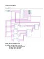
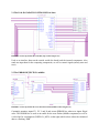
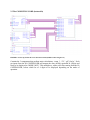
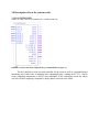
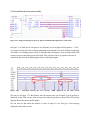
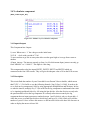
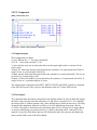
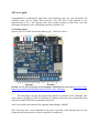
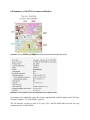
CALCULATRON
“The calculator most used by smart Alien investors!”
Developed by:
Doumet, Paul
260 226 189
Foucher, Simon
260 223 197
(G 07)
Developed for a CYCLONE II
EP2C20F256C8
FPGA Board
McGill University
December 1st, 2008
1.0 SYSTEM FEATURES
The Caluculatron is a financial calculator designed for you aliens to make wise decisions when it
comes to your financial investments. It has three important modes:
1) Computation of the future value: the calculatron is capable of calculating the future value of
any investment given the rate of interest ‘i’ offered by the bank or any other investment
company, the current present value and the number of years N.
2) Computation of the number of years needed to double your money (double time): Given the
rate of interest offered by your bank or investment company, the calculatron can give you the
number of years needed to double your money.
3) Computation of the interest rate: Given the desired Present Value, the desired Future Value
and the number of years desired the calculatron can calculate the rate of interest needed to
achieve your given goals.
Calculatron is your ticket to efficient, fast and reliable calculations. It can output any of your
desired variables in Economy’s most important formula: FV = PV*(1+i/100), where FV is the
future value, PV is the present value, ‘i’ is the rate of interest and N is the number of years of
your investment.
2.0 BLOCK DIAGRAM
FULL CIRCUIT:
FIGURE 2.1: Block diagram of the entire circuit
The calculatron can be divided into 3 major parts:
1. The IO & DATAPATH CONTROLLER (top)
2. The ERROR DETECTION (middle)
3. The COMPUTING CORE (green)
2.1 The IO & DATAPATH CONTROLLER (in blue)
FIGURE 2.2: Close up look at the controller (top section of figure 2.1)
Used as an interface between the outside world (the board) and the internal components. Also
sends out input data for the computing components, as well as control signals (mostly start and
reset)
2.2 The ERROR DETECTION (middle)
FIGURE 2.3: Close up look at the error detection circuits (middle section of figure 2.1)
Constantly monitors inputs PV, FV, I and N and asserts ERROR line when user inputs illegal
value. The ERROR line is used as an enable for the error flasher (Middle component) as well as
a select line for a multiplexer (DISPLAY_MUX, on the right) which selects either the calculated
data or a flashing ‘ERR ’
2.3 The COMPUTING CORE (bottom left)
FIGURE 2.4: Close up look at the error detection circuits (middle section of figure 2.1)
Contains the 3 components that perform major calculations: ‘comp_i’, ‘FV’, ‘g07_find_n’. Each
get inputs from the IO CONTROLLER and outputs the data, already separated in 4 digits and
ready to be displayed to ‘MODE_MUX’. This multiplexer, with a select line coming from the IO
CONTROLLER, selects which set of 4 digits to be displayed depending on the mode of
operation.
3.0 Description of how the system works
3.1 I/O CONTROLLER
[VHDL file /DSD_LAB 5/IO_INTERFACE/IO_CONTROLLER.vhd]
FIGURE 3.1: Closer look at the component IO_CONTROLLER from figure 2.1
The IO Controller is used as a main controller for the circuit as well as a sequential board
interfacing unit. It takes care of inputting data, outputting display, sending out FV, PV, I and N
to the computing components as well as start commands. It also controls the mode line which
will select which computing component’s display data to send out to the LEDs.
3.1.1
I/O CONTROLLER’s ports
3.1.1. A Board Interfacing
INPUTS:
sw: connected to the board’s 10 switches pins
key: connected to the board’s 4 switches pins
CLOCK: connected to the board’s 50 MHz clock pin
OUTPUTS:
LEDG0: Connected to the board’s green LED0, informs user that we are in mode ‘00’
LEDG1: Connected to the board’s green LED1, informs user that we are in mode ‘01’
LEDG2: Connected to the board’s green LED2, informs user that we are in mode ‘10’
LEDR0: Connected to the board’s red LED6, informs user that computation is done and
that there should be a decimal point between the rightmost digit and the second rightmost
digit. (Was originally connected to LED0, but we found out that the board’s display
points are not pinned)
hex0: Connects to the board’s leftmost digit (Our pin assignment is reversed, but so are
the signals going to the digits, to bots inversion balance out to regular display)
hex1: Connects to the board’s second leftmost digit
hex2: Connects to the board’s second rightmost digit
hex3: Connects to the board’s second rightmost digit
3.1.1. B Circuit Interfacing/ Data Lines
INPUTS:
DIG1: Inputs the data to be displayed on the board’s Digit 1. (The data is externally
multiplexed both for the mode of operation and for error detection, such that these lines contain
the appropriate result of the computation)
DIG2: Inputs the data to be displayed on the board’s Digit 2.
DIG3: Inputs the data to be displayed on the board’s Digit 3.
DIG4: Inputs the data to be displayed on the board’s Digit 4.
OUTPUTS:
PV_OUT: Sends out the value of PV to the computing components that need it to
operate, as entered via the user interface.
FV_OUT: Sends out the value of FV to the computing components that need it to
operate, as entered via the user interface
N_OUT: Sends out the value of N to the computing components that need it to operate,
as entered via the user interface
I_OUT : Sends out the value of PV to the computing components that need it to operate,
as entered via the user interface
3.1.1. B Circuit Interfacing/ Control Lines
INPUTS:
E_MODE: Since the error detection is done externally, this notifies the controller that the
value entered by the user is illegal, such that the controller can display a flashing error
instead of its regular message.
OUTPUTS:
RESET: When the user issues a reset command to the IO CONTROLLER, this line is
asserted while the command is issued and resets every synchronous component in the
whole circuit.
MODE : Is equal to the mode of operation as entered by the user. Used as a select line for
MODE_MUX; the multiplexor that selects which data to display.
START_FV: Sends out the start sequence to the component that computes FV (If the
machine is in compute FV mode)
START_DT: Sends out the start sequence to the component that computes DT (If the
machine is in compute DT mode)
START_I: Sends out the start sequence to the component that computes i (If the machine
is in compute i mode)
3.1.2
I/O CONTROLLER’s external components
COMPONENT SEGMENT_DECODER
[Relevant files in /DSD_LAB 5/SEGMENT_DECODER/]
Identical to the Segment Decoder described in Lab2 Report. It receives a 7 bit number in
binary and converts it to the sequence that will display it on the board’s LED display.
COMPONENT G07_binary_to_base100
[Relevant files in /DSD_LAB 5/compute_FV/CONVERT_B2100/]
Almost identical to G07_binary_to_base100 described in Lab4 Part1, except that this one
has a 27 bit binary input instead of 26 as designed. Its main function is to convert FV and PV to
displayable digits for the user to see (Does not play any essentially functional part of the
controller)
3.1.3
I/O CONTROLLER’s internal components and functions
FSM MACHINE
STATE: RESET
Reached asynchronously when all 4 buttons are pressed simultaneously and switch 9 is
OFF. The switch condition is because the transition out for the next state (ready) is done by
pressing button3 + sw9 ON, so had we not implemented the sw9 as a necessary condition for
reset, if the user let go of button 3 last, he would skip the ready state.
In this state, we reset PV and FV signals to 0 and N and I to 1 (because 0 is a illegal value
for N and I). We reset the mode to “11” which is an undefined mode and force the FSM to ready
state.
We also assert RESET_SIGNAL, which is sent out to all the external clocked
components and resets them.
The following states are all activated on rising clock edge.
STATE: READY
The purpose of this state is to select the mode of calculation. The first thing that is done
here is to reset “RESET_SIGNAL” to zero, in order to 'stop resetting' the external devices. When
in ready state, the controller will send out the values:
DISPLAY1 <= "0010110"; -- M(22)
DISPLAY2 <= "0000000"; -- O(00)
DISPLAY3 <= "0001101"; -- d(13)
DISPLAY4 <= "0001110"; -- E(14)
to the signal lines connected to the segment decoder, in order to display 'mode' on the screen.
In this state, if button 0 is pressed, the value of sw0 and sw1 is loaded into
“MODE_SIGNAL”. This signal is sent externally to MODE_MUX (see figure 2.4), which
selects which component's output to connect to the IO CONTROLLER's DIG[1,2,3,4] input
ports (which will eventually be sent to the segment decoders). MODE_SIGNAL is also used
further so that the controller knows in which mode it needs to operate.
The 3 modes of operation are “00” for compute I, “01” for compute FV and “10” for
compute double time (DT). They have been chosen as such because of the order in which the
components have been places in the circuit (see figure 2.4, this made it easy to look at the circuit
and extrapolate which data inputs was required by which state). As different modes are selected,
the 3 rightmost green LEDs will indicate to the user in which mode the calculator is set to.
To exit this state, the user needs to press button3 while sw9 = ON. Each state transition is
made using Button 3 + one unique switch, to avoid having many unintentional button reads. The
choice of switches might not seem incoherent to the user, but since the machine only captures the
data it needs for the selected mode of operation, it skips some states. Therefore, even though the
switches have been assigned according to the sequence of states, they do not appear sequential
from a user's perspective.
The next 8 states are used to capture user data. There are four data capture states, each
preceded buy a display data state (added last after re-reading the specs!).
In every data capture state, the controller will read the E_MODE line to know if we are in
error mode. As the user inputs the data, as soon as an out of bound value is detected (externally),
the error detecting circuitry will both warn the IO CONTROLLER of this condition and make
the DISPLAY_MUX pass the “ERR ” code generated by the error flasher, rather than the
component's output (see figure 2.3). Since these lines are hard wired back to the IO
CONTROLLER through the DIG[1.2.3.4] input ports, the IO CONTROLLER will send out that
code to the segments decoder to display a flashing error message on the board. The user will still
be able to get out of error mode by entering an allowed value.
If no error is detected, the CONTROLLER will display a number (which represents the
switch that needs to be high while button 3 is pressed; to avoid having to carry that information
on a chart), a dash, and the name of the data being entered (in, FV, PV, Yr)
To enter the data, the switches are used as raw data, and the buttons as 'load' commands.
Button 0 will load the switches into bits 9 downto 0 (6 downto 0 for I and 5 downto 0 for N), for
PV and FV, Button 1 loads bits 19 downto 0 and button 2 loads bits 26 downto 20. The data can
be modified as long as the user is in this state.
As soon as the user inputs a load command, the FSM will switch to “display data” mode
and momentary display the data that just got entered. This state is entered with a timer and exits
when the timer reaches zero (to avoid being in that state for milliseconds). The timer is also used
to know when to send out the start = 0 and start = 1 commands that will initiate the binary to
base 100 converter that will convert PV and FV into displayable data.
STATE: input_FV
If we are not in mode “00”, the FSM jumps to the next state as soon as it enters this state
(since compute I is the only operation which requires a FV).
If at any point an error is detected, the controller will pass a flashing “ERR” to the LEDs
(as described above), otherwise the controller will send:
DISPLAY1 <= "0001000"; -- SWITCH 8 TO PROCEED (08)
DISPLAY2 <= "0100101"; -- -(37)
DISPLAY3 <= "0001111"; -- F(15)
DISPLAY4 <= "0011110"; -- V(30)
Which means: (Button 3 AND) Switch 8 to proceed – enter FV
When data is entered, the FSM will reset the display timer and to go display_fv mode.
When button 3 is pressed while sw8 = ON, the FSM will go to state input_PV.
STATE: display FV.
When in this state, the controller will convert FV to displayable digits and display them
on the board. When the state is entered, the controller will issue a start = 0 command to the
convert to base 100 component. On the next count (next clock cycle), the controller will issue
start = 1 to the converter to initiate the conversion. Once the couter reaches zero, the FSM will
go back to 'input_FV' state.
STATE input_PV
This state is identical to input FV, except that the FSM will remain here if in mode
compute I and compute FV. Otherwise, the transition will be made to state input_i. Also, this
state manages the PV data vector, and displays
DISPLAY1 <= "0000111"; -- (07)
DISPLAY2 <= "0100101"; -- -(37)
DISPLAY3 <= "0011001"; -- P(25)
DISPLAY4 <= "0011110"; -- V(30)
Which means (button 3 AND) sw(7) – enter PV.
STATE display_PV
Copied and pasted from display FV, but managing PV data.
STATE input_i;
The FSM will stay here if MODE_SIGNAL is 01 (compute FV) or 10 (compute DT)
This state will manage the 7 bit i_signal vector and displays
DISPLAY1 <= "0000110"; -- sw toggle(06)
DISPLAY2 <= "0100101"; -- -(37)
DISPLAY3 <= "0000001"; -- i(01)
DISPLAY4 <= "0010110"; -- n(22)
for sw(6) to proceed and -in for interest rate.
STATE display_i
As soon as data is entered in state input_i, the controller will enter this state which is very
similar to display FV and PV, except that here, there is no need to use the binary to base 100
converter as SIGNAL_i can be directly fed into the decoder. Also, since the interest only takes
up at most a single digit on the display board, we've added “in=” as the first 3 digits (to enhance
user experience)
STATE: input_N
Very similar to input_i, except that the controller stays here only if MODE_SIGNAL =
"01" or MODE_SIGNAL = "00" (otherwise, goes to state start1). Also, this state managed the
N_SIGNAL vector and displays:
DISPLAY1 <= "0000101"; -- SW5 TO PROCEED (05)
DISPLAY2 <= "0100101"; -- (37)
DISPLAY3 <= "0100010"; -- Y(34)
DISPLAY4 <= "0011101"; -- R(29)
if the system is not in error mode.
When button 3 is pressed while sw(5) = ON, the FSM goes to state start1.
STATE: display_N
Very similar to display_i, except that since we display a 6 bit vector in a 7 bit segment
decoder, we add a 0 as the MSB. We also display “YR=” as the first 3 digits.
The data signal lines are connected to external ports of the controller, so as the data is
inputted by the user, it instantly reaches all the computing components that will require them for
proper operation. Therefore, at this point, the component corresponding to the mode of operation
has its data, the data values are within legal range and the display multiplexer is letting through
that component's result, already segmented on 4 digits and already fed back to the IO
CONTROLLER through input ports DIG[1,2,3,4].
The next 2 states issue a launch signal to the appropriate component.
STATE: start1
This state will innate the launch signal for the required component for the operation
selected.
IF MODE_SIGNAL = "00" THEN START_i <= '0';
IF MODE_SIGNAL = "01" THEN
START_FV <= '0';
IF MODE_SIGNAL = "10" THEN START_DT <= '0';
ELSE
If there were no mode signal = “11” (this condition is filtered earlier, but we added this as a
second safeguard), go back to ready state.
Once we sent out s start = 0 signal, move on to state start2.
STATE: start2
This state completes the initiation of the start sequence by sending out start = 1 to the
appropriate component, based on the mode of operation.
IF MODE_SIGNAL = "00" THEN
START_i <= '1';
IF MODE_SIGNAL = "01" THEN
START_FV <= '1';
IF MODE_SIGNAL = "10" THEN START_DT <= '1';
Afterwards, the FSM goes to the display state.
STATE: display_result;
Since earlier on, the controller communicated various messages to the user via the
segment decoders, this state is used to finally link the computed result to the board's LED. The
result of the computation is hard wired into input ports DIG[1,2,3,4] and gets passed to the
segment decoder.
The controller also lights up red LED 6, both to notify the user that the result has been
computed, and to remind him of the decimal point (since the board's points are not pinned)
At this point, to start over, the user has to launch a reset command.
3.2 Computing interest rate (comp_i component)
[VHDL file /DSD_LAB 5/ compute_i/ comp_i.vhd]
FIGURE 3.2.1: Closer look at the component comp_i from figure 2.1
comp_i’s ports
INPUTS:
Reset: Initiates a system reset, sent from the IO CONTROLLER
clk: Connected to the circuit's 50 MHz clock
start: Receives a start command from the IO CONTROLLER
Input_FV: FV Data vector from the CONTROLLER
Input_PV: PV Data vector from the CONTROLLER
Input_N: N data vector from the CONTROLLER
OUTPUTS:
DONE: Notifies that the computation is done (not used)
D1is: Left most digit of the computed result (to be displayed)
D2is: Left most digit of the computed result (to be displayed)
D3is: Left most digit of the computed result (to be displayed)
D4is: Left most digit of the computed result (to be displayed)
3.2.1 comp_i’s external components
Nth_Root_Machine
[Relevant files in /DSD_LAB 5/Nth_Root_MACHINE/]
Nth_Root_Machine identical to the Nth Root Device described in LAB 4. This
component inputs a number X, takes its Nth root and outputs the result already converted to 4
digits.
LPM_DIVIDE
[Component declared in the lpm library]
This component (for our use) divides the data presented on the FV lines by the data on
the PV lines. We only take note of the result of the division (the remainder is ignored).
comp_i’s internal components and functions
This component has a few asynchronous parts.
The LPM_DEVIDE is permanently wired to the FV DATA, and divides it by PV. The FSM
looks at the result whenever it needs it.
Also, the output ports are connected to '0' for the leftmost digit (since the interest rate will
be computed as x.xx in base 100)
FINITE STATE MACHINE (CONTROLLER)
STATE: S0 (reset state)
When the Reset port gets a 1 from the IO CONTROLLER, the state of the FSM is set to
S0 and the Nth_Root_Machine is reseted. The function of state 0 is to set DONE = 1, to notify
the outside world that no work is being accomplished at the moment, then the state transitions to
S1
STATE: S1 (wait for start 0)
In this state, the FSM waits for start = 0. This command is sent by the IO
CONTROLLER. As soon as start = 0, the FSM state gets set to state S2
.
STATE: S2 (wait for start 1)
In this state, we prepare the data presented in the input ports by the IO CONTROLLER
for division by converting PV and FV to sdt_logic_vectors for the LPM_DIVIDE component,
the we go to state 3.
STATE: S3 (Prepare to take the Nth Root)
The initial design of this component use to estimate the time required to take the Nth root
based on the size of N.
To so so, we calculated the worst time scenario, and best case scenario to give us a ball
park estimate of how much time it requires to produce a stable result. We estimated a worst case
(when taking the 63rd root of 99, see figure 3.2.2) took roughly 90 uS on a 37nS clock, so 2 432
clock pulses.
FIGURE 3.2.2: Worst case time requirement to take the Nth Root. Here, taking the 63rd Root of 99, we can
observe output stability of the last digit (DIGIT4) and the answer vector (implemented for testing) at roughly
90 uS
The best case (shortest time) result (taking the 1st root of 99, see figure 3.2.3) took
roughly 4.65nS on a 37nS clock. From this data, we can estimate that the fastest operation can be
completed in roughly 126 clock pulses.
FIGURE 3.2.3: Best time case time requirement to take the Nth Root. Here, taking the 1st Root of 99, we can
observe output stability of the last digit (DIGIT4) and the answer vector (implemented for testing) at roughly
4.6 uS
From this data, we made a basic linear approximation as follows:
[(MAX2432) / (NMAX63 – NMIN1 )] + 126 = (39 *N + 126) clock pulses given N. To be
conservative and avoid unpleasant surprises, we used 40 instead of 39.
In order to validate this estimate, we looked at a middle value (31st root of 99) and tested
our formula.
Clock pulses required = 126 + N*40
Clock pulses required = 126 + (31)*40 = 1366
Running a Quartus simulation, we found that this operation is stabilized within 50nS on a 37nS
clock (see figure 3.2.4), so within 1352 pulses, which is within our estimate.
FIGURE 3.2.4: Middle time requirement to take the Nth Root. Here, taking the 31st Root of 99, we can
observe output stability of the last digit (DIGIT4) and the answer vector (implemented for testing) at roughly
49.9 uS
In the end, all that work got thrown out and we opted for a more optimal hand shaking
mechanism between the Nth_Root_Machine and the comp_i component. Because of the way
Nth_Root was designed, it's DONE signal = 1 after a reset (to notify that no work is being done).
Since we will be listening to this done signal to find out when the operation is done, we
implemented a signal called 'WFD' (Wait for Done). This signal is simply used as a 3 bit counter
that counts from 7 to 0. We chose a 3 bits counter because we know that when a work order is
sent out to the Nth_Root_Machine, it takes 2-3 clock pulses to initialize before Done is reset to
0, and that the start sequence might take 2 more pulses (start 0, start 1). A 3 bit counter (7 to 0) is
large enough to accommodate for this overhead, and allows flexibility to be reused for
implementing other similar components (like the convert to binary).
So in state 3, we set WDF = 7 and go to state 4. This state is also used as a time buffer to
give time for the LPM_DIVITE to finish the division and for the result to travel to the input of
the Nth root component.
STATE: S4
Prepare the Nth_Root initiation by setting Nth_ROOT_ENABLE = 0 (connected to the
Nth Root start port)
STATE: S5
Finish initiating the Nth root operation by setting Nth_ROOT_ENABLE <= '1'. This state
also decrements WDF by 1. The FSM is locked into this state until WDF reaches 0. At this point,
it transitions to S6.
STATE: S6
At this point, the Nth root operation is on its way and DONE from the
Nth_Root_Machine has been reset to 1 to indicate that computation is happening. The FSM
waits in this state until Nth_ROOT_DONE = '1', then goes to S7.
STATE: S7
The Nth_Root_Machine outputs data already separated into digits (see figure 3.2.5), so
the only thing left to do is to subtract 1 from the interest rate calculated.
The digit signals are are connected to the comp_i's output ports D1is, D2is, D3is, D4is,
which make their way back to the IO CONTROLLER (See controller's description for more
details), so after the substation is done, the process is done. The FSM goes back to state 0.
FIGURE 3.2.5: The output of the Nth_Root_Machine comes already seperated into digits. In this example,
taking the square root of 2 dosplays 1-BLAKK-41-41, which represents 1.4141
3.3 Error detection component
[F:\DSD_LAB 5\ERROR_FINDER]
Figure 3.3.1 : Picture of our error finder component
3.3.1 Cases of error
This component sends an error signal whenever one of our inputs (Future Value, Present Value,
N the number of years or i the interest) are out of range.
1) Error gets assigned ‘1’ whenever the Future Value entered by the user is bigger than
100000000.
2) Error gets assigned ‘1’ whenever the Present Value entered by the user is bigger than
100000000.
3) Error gets assigned ‘1’ whenever the interest ‘i’ is bigger than 99 or equal to 0.
4) Error gets assigned ‘1’ whenever the number of years N is 0. N can never exceed 63 since N
has only 5 bits (‘11111’ = 63).
3.3.2 Waveforms
Figure 3.3.2:
Waveforms showing how the error signal gets assigned ‘1’ when the interest go out of bound.
Figure 3.3.3: Waveforms showing how the error signal gets assigned ‘1’ when the interest go out of bound.
We can see in Figure 3.3.2 that when our input N is equal to 0 our error signal is equal to ‘1’ and
when N gets assigned 1 afterwards the error signal goes back to ‘0’.
We can also see in figure 3.3.3 that when our interest is higher than 100, our error signal gets
assigned ‘1’.
3.3.3 Overall circuit of our error scroller
Figure 3.3.4 : Diagram showing how the error signal is transmitted throughout the overall circuit.
In Figure 3.3.4 when one of our inputs is out of bound, our error signal will be equal to ‘1’. This
error signal is fed to the error scrolling component created in lab3. Our error flashing component
will send a error flashing signal to the I/O controller that will display a error message on the LED
screens as soon as the inputs go out of bounds. This will not in any way stop the processes of
calculation, But instead of displaying the answer with illegal inputs.
Figure 3.3.5 : Waveform showing the error message ‘ERR’ displayed on the LED screens
We can see in Figure 3.3.5 that shortly after the interest gets out of bound, a error message is
displaced on the LED screens; And as soon as the interest gets back in bound The LED screens
displays the answer that it should display.
We can also see that when the number of years is equal to 0 we also get a error message
displayed on the LED screens.
3.4 N calculator component
[DSD_LAB5/compute_DT/]
Figure 3.4.1: Number of years calculator component.
3.4.1 Inputs/Outputs
This Component has 4 inputs:
1) reset: When reset = ‘1’ the code goes to the initial state.
2) CLK : clock with a period of 37 nS.
3) start: start has to go low at some point after reset has gone high so it can go from a state to
another.
4) Input_interest : The interest can only go from 1 to 99 which means Input_interest can only go
from “0000001” to “ 1100011”. This input is 6 bits long.
This component has also four inputs DIGIT1, DIGIT2, DIGIT3 and DIGIT4 which are
connected to the four LED screens. They will give the adequate value of N on the LED screens.
3.4.2 Description
This circuit finds the number of years N needed for our Present Value to double, which means
that FV/PV = 2. To find N we use the following formula: [log (2)/log (1+i/100)]. In order to do
so we feed our log component (i/100) by using appropriate multiplications and divisions. In fact,
we take the interest, multiply it by 2^11(in order for the log component to understand what value
we’re inputing) and then divide it by 100 using the lpm divider. After the division we only take
the quotient and feed it to the log component. It is already taken into account by the log
component that our input represents a number between 1 and 2 which is why we do not add a 1.
After that we use a second lpm divider to divide log2 and log of (1+i/100) which will yield the
number of years N. Once we have this answer we still need to feed it to the base 100 converter in
order to display the answer in base 100.
3.4.3 Summary of Description
Overall to find N:
1) Take the input, multiply it by 2^11 which will be understood as our interest ‘i’ by the log
component.
2) Take the result of the multiplication and divide it by 100 using an lpm divider so that we can
input i/100 to our log component. Again we do not need to add a 1 because it is taken into
account by the component.
3) Using a second lpm divider we divide log of 2 and log of (1+i/100) which will yield the
answer N.
4) The final step will be to feed our answer N to the base 100 converter.
Note: When converting to base 100 we use a WFD signal. This WFD signal is used in order to
avoid our VHDL code to jump from a state to another too quickly. In fact it is used to ignore the
Done signal of the Nth root when it is done with its calculations. See more in Control
inputs/outputs.
3.4.3 Waveforms
Figure 3.4.2: Waveform showing the resulting number of years displayed on the LED screens
In this waveform we have an interest of 10%, if we use a calculator we will find the answer to be
7.29 which is what is displayed on the waveform in ‘Answer’. 7 is displayed on the 3rd LED
screen while 29 get displayed on the 4th LED screen.
3.5 FV Component
[DSD_LAB/compute_FV/]
Figure 3.5.1: Future Value calculator component.
3.5.1 Inputs/Outputs
This component has 6 inputs:
1) reset: When reset = ‘1’ our state is initialized.
2) CLK : clock with a period of 37 nS.
3) start: start has to go low at some point after reset has gone high so that we can move from
state to state.
4) Input_PV: Enters the Present value desired by the consumer, it is represented with 26 bits. It
can go as low as 0 and as high as 999999.99
5) Input_interest: Enters the interest desired by the consumer, it is represented with 7 bits. It can
go as low as 1% and as high as 99%
6) Input_N: Enters the number of years desired by the consumer, it is represented with 6 bits. It
can go as low as 1 year and as high as 63 years.
The outputs of the components are DIGIT1, DIGIT2, DIGIT3 and DIGIT4 which are connected
to the four LED screens. They will give the adequate value of FV on the LED screens.
3.5.2 Description
The component takes the interest, the present value and the number of years as input and outputs
the future value. In order to do this calculation, we add 100 to our interest. If N > 0 we multiply
our interest (100+i) with our present value. After multiplying we divide the answer by 100 using
an lpm divider component, therefore it will be as if we are multiplying the present value by
(1+i/100). After that we decrement our N and check again if N>0. As long as N is bigger than 0
we keep on multiplying our present value by (1+i/100) as described earlier. Otherwise if N is
equal to 0 we get our final answer that we will feed into the base 100 converter and display the
answer on the LED screen of the Altera Board.
Note: If we want 10 as our present value, we multiply it by 100 to be able to represent the
fractional part in the output and on the altera board.
Example: if we want 5 as our present value, we enter 500 on the altera board. Using a present
value of 500 will yield to a Future value of 805.225 if our interest is 10% and the number of year
is 5, whereas a present value of 5 will yield a future value of 8.05. Our calculator in this case will
take the integer part of our modified Present value (which represents the full answer of our real
present value) and display it on the LED screens in base 100. In this example it will display 805
in base 10.
3.5.3 Summary of Description
Overall to find FV:
1) add 100 to the interest.
2) Check if N > 0, if yes then multiply the result in 1) by the Present Value x 100.
3) Divide answer in 2) by 100 and decrement N.
4) go back to 2) to check if N > 0 if yes then keep on going from step 2 to 4 until N = 0.
That way our PV*(1+i/100) is going to get multiplied by itself N times.
5) If N = 0 feed the overall answer to the base 100 Converter and output will be fed to the Altera
Board.
Waveform
Figure 3.5.2 : Waveform displaying the value of value of the Future value onthe LED screens.
In this Waveform we set our input interest to 10%, our Present value to 10000(which means that
we have a present value of 100) and our number of years N to 5. The Answer is 16105.1(using a
calculator). We take the integer part of this answer and display it on the LED screens as shown in
the waveform: Digit 1 gets assigned 0, Digit 2 gets assigned 1, Digit 3 gets assigned 61 and Digit
4 gets assigned 5. This answer is correct since the future value of a present value of 100 should
yield to 161.05.
.
4.0 User’s guide
Congratulations for making the right choice and purchasing your very own calculatron, the
calculator most used by smart Alien investors! You will find it both pleasant to use,
ergonomically fit for a 100 fingered alien, and versatile enough to make most every day
investment calculations, like evaluating the purchase of planets, etc…
4.1 Getting started
Unpack your CYCLONE II board and load up “g07_LAB5.sof” onto it.
FIGURE 4.1: The Altera board pins ans switch numbers. (Modified picture taken from http://www.cizgitagem.org/e-market/upload/product/altera-de1/DE1_intro_500x.png)
The first thing to do once the program has started is to send out a reset command. This
can be done by having sw9 OFF and pressing all 4 buttons. Once the reset command has been
activated, all the LEDs will be momentarily turned off.
After a successful reset command, the segments should display “MODE”.
Note: You may issue a reset command at any point to get back to the starting point. (In case
wrong data has been entered, or when an operation is completed)
4.2.1 Inputting Data
Button 0 will load the binary data interpreted from the switches (9 to 0) to the least
significant bits of what is being inputted. To help the user follow the operations, the LED will
display what is being inputted (FV, PV,in,YR).
In the case of loading values that are smaller than 10 bits (mode, years and interest), only
the rightmost switches will be read to the extent of the size of the data (mode will only look at
switches 0 and 1, year will look at the 6 rightmost switches, interest will read the 7 rightmost
switches).
For values greater than 10 bits (PV and FV), press button 1 to load the switches into bits
19 down to 10, and button 2 to load the 7 rightmost switches into bits 26 down to 20 of what is
displayed on the screen.
4.2.2 Flowing through the operations
Switching between states (mode select, data input and calculation) is done using button 3
in combination with a single switch. When inputting data, the LED will display which switch to
turn ON to get to the next state (For example, if the screen displays “7-FV”, this means that
pressing buttons 2,1 and 0 will input data into FV, and when done, pressing button 3 while
switch 7 is ON will go to the next state. If the screen displays “8-YR”, button 0 will load data
into ‘years’ and to get to the next state, the user needs to press button 3 while switch 8 is ON)
After a reset, to get out of “MODE” state, press button 3 while switch 9 is ON (the
leftmost switch)
4.2.3 Modes of operation
Your new calculatron can handle 3 modes of calculation:
MODE 00: Compute an interest rate given a Present Value, a Future Value, and N (number of
years)
MODE 01: Compute a Future Value, given a Present Value, interest and N
MODE 10: Compute the time required to double capital given an interest rate i
Once a mode of operation has been selected, it will appear as a lit green LED on the right
hand side of the board. The rightmost LED means mode 00, the second rightmost LED meand
mode 01 and the 3rd LED signified mode 10.If you want to change mode at any other time than
when in MODE state, a system reset will be required.
4.2.4 An example
1 – Reset the system by pressing all 4 buttons simultaneously while switch 1 is OFF. (Pressing
the center buttons first works best). After a reset, the display should read “MODE”
2 – Enter the mode of operation. For this example, we will compute FV, so set the rightmost
switches to “01” and press button 0.
Once the mode is selected, the second rightmost LED should be lit.
Note: you can change the mode of operation as many times as you wish while in “MODE” state.
3 – Go to input data.
Set the leftmost switch to 1 and press button 3. The screen should now read 7-PV. This means
that the calculatron is expecting a PV, and that to get to the next state, switch 7 will have to be
ON while pressing button 3.
4- Set the switches to “0001100100” and press button 0. This will load “1.00” as a present value.
While button 0 is pressed, the screen will read “BALNK BLANK 1 0”, which means that PV is
now set to 1,0.
Note: If you enter a PV out of bounds, error will start flashing, but you can get rid of it by
reloading a lower value while into that state. A reset is not needed.
Also, you may change the value of PV while button 0,1, or 2 is pressed an see what FV is being
set to.
5 – Set switch 7 to ON and press button 3 to go on. The screen should now read “6-in”. This
means that the calculatron is expecting an interest rate, and that to get to the next state, switch 6
will have to be ON while pressing button 3.
6 - Set the switches to “xxx0000000” and press button 0. While button 0 is pressed, you’ll see
in=0, meaning that you loaded 0 as an interest rate. Since N is an illegal value for the years, error
will start to flash indicating error mode.
Now set the switches to “xxx0001010” and press button 0. This will load “10” as an interest rate
(while button 0 is pressed, you’ll see “in=A”)
Note: If you enter an interest rate out of bounds, error will start flashing, but you can get rid of it
by reloading a lower value while into that state. A reset is not needed.
7 – Set switch 6 to ON and press button 3 to go on. The screen should now read “5-YR”. This
means that the calculatron is expecting N (Year), and that to get to the next state, switch 5 will
have to be ON while pressing button 3.
8 - Set the switches to “xxxx000010” and press button 0. This will load “2” as the number of
years over which to compound the interest. While button 0 is pressed, the screen will display
“Yr=2”.
Note: By default, N is set to 1. Since the calculator only reads the 6 rightmost switches, the only
out of range value we can have (between 1 and 63) is 0. If you entered 0 as a period, error will
start flashing, but you can get rid of it by reloading any other value while into that state. A reset
is not needed.
9 – Set switch 5 to ON and press button 3 to go on. The screen will now display “BLANK
BLANK 1 L” and a red LED will be lit. The red LED roughly represents the decimal point on
the board. (For some reason, the Altera people never assigned a pin to the decimal points on the
board).
The answer can be interpreted as 1.L in base 100, which is 1.21 in base 10.
10 – To start over, reset the system.
Note: Remember to have switch 9 OFF before issuing a reset command with the 4 buttons. This
is because button3 and sw9 ON will exit “MODE” state. If a user issues a reset command while
switch 1 is ON and button one gets let go last, the system will transit to the next state
immediately, which could cause user confusion.
Note: remember that some digits had appeared twice in the original base 100 number system
presented in the lab2 description, so 3 of the digits have been changed from the table presented in
lab2, based on comments made in the DSD discussion board.
5.0 Testing the circuit
In order to test our whole system we tried many different inputs for each one of our modes to
make sure that each one of them was working perfectly fine. These here are some of the of the
tests we performed on our system:
1) Testing of the Future Value Calculation: In order to test this we chose our Present Value to be
10$(therefore our input was 1000 as stated above), our interest rate to be 15% and our number of
years to be 3.
Using a calculator the value of our future value was 15.20875$.
Using our Altera Board the value displayed on the LED screen was
base 100 and the rightmost symbol represents 20 in base 100.
. ‘F’ represents 15 in
The error here is (15.20875-15.20)*100 = 0.8%
2) Testing of the Interest Rate Calculation: In order to test this we chose our Future Value to be
300$, our Present Value to be 100$ and the number of years to be 5.
Using a calculator the value of the interest was: 24.57309%
Using our Altera Board the value displayed on the LED screen was
. The leftmost
symbol represents 24 in base 100 and the rightmost symbol represents 57 in base 100.
The error is (24.57309-24.57)*100 = 0.4%
3) Testing of the double time: In order to test this we chose the interest rate to be 37% and we
already know that (Future Value)/ (Present Value) is equal to 2.
Using a calculator the double time was 2.2017 years.
. The Leftmost
Using the Altera Board the value displayed on the LED screens was:
symbol represents a 2 in base 100 and the rightmost symbol represents a 21 in base 100.
The error is: (2.21-2.20170)*100 = 0.8%
6.0 Summary of the FPGA resource utilization
FIGURE 6.1: Top view of the pin assignments on the Cyclone II board used by the circuit.
FIGURE 6.2: Flow summary after full compilation of the complete circuit
According to the compilation report, the circuit is implemented with 601 registers and 3145 logic
elements, roughly 17 % of the board’s capacity.
The I/O interface occupies a total of 47 pins (15%), and the ROM table used for the log2
component takes 32 kb of RAM.
7.0 Conclusion
We didn’t encounter any major issues during the design process. Everything was well
thought out and drawn out on paper before we built the circuit, and besides a few compilation
errors and minor issues, everything went very well and we had the board working after less than
2 hours of tweaking.
Some of the minor issues we encountered are as follow.
When we first inputted the board, the connections to the LEDs were backwards. It got
easily solved by switching the signals (You may notice in the controller that DIG1 is assigned to
DIGIT4, etc…) This had to be done because of improper pin assignments made in previous labs,
and it was much simpler to inverse the 4 display bus signals than to redo the pin assignment.
Also, originally, every input value was reset to 0, but when N = 0, the error detector
detects an error and automatically displays “ERR” on the screen, regardless of the state, This was
fixed by resetting N = 1.
We also ran into a timing issue between machine time and human time. Originally,
button3 was suppose to be used alone to detect a state change, but when the user pressed button 3
in human time (say for ½ second), the process read it at every clock pulse and sent the machine
into computation mode within a few milliseconds. Instead of implementing a timer, we found it
simpler to couple the button 3 press with a unique switch flag.
Once everything was working, we spent quite a bit of time enhancing the user experience
by displaying information on the screen. The original idea was to have button3 and sw9 to go to
state 2, then button 3 and sw8 to go to state 3, then button 3 and sw7 to go to state 4, etc… But,
since the process goes through all the input states (FV, PV, I,N) but only stays into the states it
needs for the mode selected, different modes yielded different switch order (as one might notice
while navigating through the calculator states). We found that displaying which switch to
activate while pressing button 3 was the most convenient way for the user to remember (instead
of having to look up a chart all the time).
We also had the issue of miss reading the system’s requirements of displaying data as it is
inputted. This was quickly resolved by implementing new “display” states while data is inputted.
Another problem arose when we were almost done testing our whole design : we realized
by re-reading the lab carefully that we omitted the part where the inputs entered by the consumer
must be displayed on the screens. This was very easily fixed due to the fact that our design is
extremely flexible and any change can be made very easily.
One unpleasant issue we encountered at the end of the design is that Altera never
assigned any pins to the decimal points on the LED display. We had seen them and waited until
the very end of the design to implement them by looking up the user’s manual (an added bonus
for the aliens!), only to find out that they were not accessible. We worked around it by lighting
up a red LED roughly under where the point was to be displayed.
In order to improve our design we could have added more components to it like calculating the
Future value, Number of years and interests with annuities. But due to time constraints we are
more than happy to have our current design work to perfection and our alien customers will be
quite pleased with the effectiveness of our calculator !