1
WWW.MWFTR.COM
ALTERA LABORATORY EXERCISES/DIGITAL_LOGIC/DE2/VERILOG
Laboratory Exercise 1
Switches, Lights, and Multiplexers
The purpose of this exercise is to learn how to connect simple input and output devices to an FPGA chip and
implement a circuit that uses these devices. We will use the switches SW17−0 on the DE2-series board as inputs
to the circuit. We will use light emitting diodes (LEDs) and 7-segment displays as output devices.
Part I
The DE2-series board provides 18 toggle switches, called SW17−0 , that can be used as inputs to a circuit, and
18 red lights, called LEDR17−0 , that can be used to display output values. Figure 3 shows a simple Verilog module
that uses these switches and shows their states on the LEDs. Since there are 18 switches and lights it is convenient
to represent them as vectors in the Verilog code, as shown. We have used a single assignment statement for all 18
LEDR outputs, which is equivalent to the individual assignments
assign LEDR[17] = SW[17];
assign LEDR[16] = SW[16];
...
assign LEDR[0] = SW[0];
The DE2-series board has hardwired connections between its FPGA chip and the switches and lights. To use
SW17−0 and LEDR17−0 it is necessary to include in your Quartus II project the correct pin assignments, which are
given in the DE2-series User Manual. For example, the manual specifies that on the DE2 board, SW0 is connected
to the FPGA pin N25 and LEDR0 is connected to pin AE23. On the DE2-70 board, SW0 is connected to the FPGA
pin AA23 and LEDR0 is connected to pin AJ6. Moreover, on the DE2-115 board, SW0 is connected to the FPGA
pin AB28 and LEDR0 is connected to pin G19. A good way to make the required pin assignments is to import into
the Quartus II software the file called DE2_pin_assignments.qsf for the DE2 board, DE2_70_pin_assignments.qsf
for the DE2-70 board, or DE2_115_pin_assignments.qsf for the DE2-115 board, which is provided on the DE2Series System CD and in the University Program section of Altera’s web site. The procedure for making pin
assignments is described in the tutorial Quartus II Introduction using Verilog Design, which is also available from
Altera.
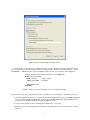
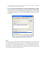
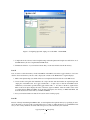
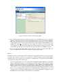
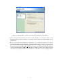
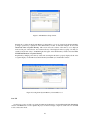
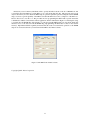
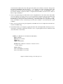
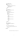
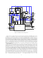
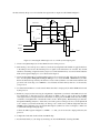
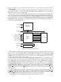
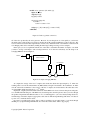
When importing the pin assignments file for the DE2-70 board, it is important to use Advanced Import Settings. To do so, click the Advanced... button on the Import Assignments screen as shown in Figure 1. Then,
check Global assignments check box as shown in Figure 2 and press the OK button. Please note that omitting
this step on a DE2-70 board may cause a compile time error.
Figure 1. DE2-70 Import Assignments window.
1
Figure 2. DE2-70 Advanced Import Settings window.
It is important to realize that the pin assignments in the .qsf file are useful only if the pin names given in the
file are exactly the same as the port names used in your Verilog module. The file uses the names SW[0] . . . SW[17]
and LEDR[0] . . . LEDR[17] for the switches and lights, which is the reason we used these names in Figure 3.
// Simple module that connects the SW switches to the LEDR lights
module part1 (SW, LEDR);
input [17:0] SW;
// toggle switches
output [17:0] LEDR; // red LEDs
assign LEDR = SW;
endmodule
Figure 3. Verilog code that uses the DE2-series board switches and lights.
Perform the following steps to implement a circuit corresponding to the code in Figure 3 on the DE2-series board.
1. Create a new Quartus II project for your circuit. If using the Altera DE2 board, select Cyclone II EP2C35F672C6
as the target chip, which is its FPGA chip. Select Cyclone II EP2C70F896C6 if using the DE2-70 board.
Or, select Cyclone IV EP4CE115F29C7 if using the DE2-115 board.
2. Create a Verilog module for the code in Figure 3 and include it in your project.
3. Include in your project the required pin assignments for the DE2-series board, as discussed above. Compile
the project.
2
4. Download the compiled circuit into the FPGA chip. Test the functionality of the circuit by toggling the
switches and observing the LEDs.
Part II
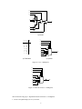
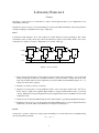
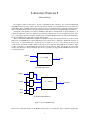
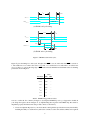
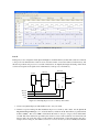
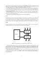
Figure 4a shows a sum-of-products circuit that implements a 2-to-1 multiplexer with a select input s. If s = 0 the
multiplexer’s output m is equal to the input x, and if s = 1 the output is equal to y. Part b of the figure gives a
truth table for this multiplexer, and part c shows its circuit symbol.
x
m
s
y
a) Circuit
s
s
m
0
1
x
y
x
y
b) Truth table
0
1
m
c) Symbol
Figure 4. A 2-to-1 multiplexer.
The multiplexer can be described by the following Verilog statement:
assign m = (∼s & x) | (s & y);
You are to write a Verilog module that includes eight assignment statements like the one shown above to
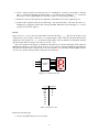
describe the circuit given in Figure 5a. This circuit has two eight-bit inputs, X and Y , and produces the eight-bit
output M . If s = 0 then M = X, while if s = 1 then M = Y . We refer to this circuit as an eight-bit wide 2-to-1
multiplexer. It has the circuit symbol shown in Figure 5b, in which X, Y , and M are depicted as eight-bit wires.
Perform the steps shown below.
3
s
x7
y7
0
x6
y6
0
1
1
m7
m6
s
X
Y
x0
y0
0
1
8
0
8
M
1
8
m0
a) Circuit
b) Symbol
Figure 5. A eight-bit wide 2-to-1 multiplexer.
1. Create a new Quartus II project for your circuit.
2. Include your Verilog file for the eight-bit wide 2-to-1 multiplexer in your project. Use switch SW17 on the
DE2-series board as the s input, switches SW7−0 as the X input and SW15−8 as the Y input. Connect the
SW switches to the red lights LEDR and connect the output M to the green lights LEDG7−0 .
3. Include in your project the required pin assignments for the DE2-series board. As discussed in Part I,
these assignments ensure that the input ports of your Verilog code will use the pins on the FPGA that are
connected to the SW switches, and the output ports of your Verilog code will use the FPGA pins connected
to the LEDR and LEDG lights.
4. Compile the project.
5. Download the compiled circuit into the FPGA chip. Test the functionality of the eight-bit wide 2-to-1
multiplexer by toggling the switches and observing the LEDs.
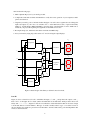
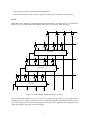
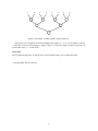
Part III
In Figure 4 we showed a 2-to-1 multiplexer that selects between the two inputs x and y. For this part consider a
circuit in which the output m has to be selected from five inputs u, v, w, x, and y. Part a of Figure 6 shows how
we can build the required 5-to-1 multiplexer by using four 2-to-1 multiplexers. The circuit uses a 3-bit select input
s2 s1 s0 and implements the truth table shown in Figure 6b. A circuit symbol for this multiplexer is given in part c
of the figure.
Recall from Figure 5 that an eight-bit wide 2-to-1 multiplexer can be built by using eight instances of a 2-to-1
multiplexer. Figure 7 applies this concept to define a three-bit wide 5-to-1 multiplexer. It contains three instances
of the circuit in Figure 6a.
4
s2
s1
s0
u
v
0
0
1
w
x
1
0
m
1
0
1
y
a) Circuit
s2 s1 s0
m
0
0
0
0
1
1
1
1
u
v
w
x
y
y
y
y
0
0
1
1
0
0
1
1
0
1
0
1
0
1
0
1
s2
s1
s0
u
v
000
001
010
011
100
w
x
y
b) Truth table
c) Symbol
Figure 6. A 5-to-1 multiplexer.
s2
s1
s0
U
V
W
X
Y
3
3
3
3
000
001
010
011
100
3
M
3
Figure 7. A three-bit wide 5-to-1 multiplexer.
Perform the following steps to implement the three-bit wide 5-to-1 multiplexer.
1. Create a new Quartus II project for your circuit.
5
m
2. Create a Verilog module for the three-bit wide 5-to-1 multiplexer. Connect its select inputs to switches
SW17−15 , and use the remaining 15 switches SW14−0 to provide the five 3-bit inputs U to Y . Connect the
SW switches to the red lights LEDR and connect the output M to the green lights LEDG2−0 .
3. Include in your project the required pin assignments for the DE2-series board. Compile the project.
4. Download the compiled circuit into the FPGA chip. Test the functionality of the three-bit wide 5-to-1
multiplexer by toggling the switches and observing the LEDs. Ensure that each of the inputs U to Y can be
properly selected as the output M .
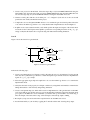
Part IV
Figure 8 shows a 7-segment decoder module that has the three-bit input c2 c1 c0 . This decoder produces seven
outputs that are used to display a character on a 7-segment display. Table 1 lists the characters that should be
displayed for each valuation of c2 c1 c0 . To keep the design simple, only four characters are included in the table
(plus the ‘blank’ character, which is selected for codes 100 − 111).
The seven segments in the display are identified by the indices 0 to 6 shown in the figure. Each segment is
illuminated by driving it to the logic value 0. You are to write a Verilog module that implements logic functions
that represent circuits needed to activate each of the seven segments. Use only simple Verilog assign statements
in your code to specify each logic function using a Boolean expression.
0
c2
c1
c0
5
7-segment
decoder
6
4
2
3
Figure 8. A 7-segment decoder.
c2 c1 c0
Character
000
001
010
011
100
101
110
111
H
E
L
O
Table 1. Character codes.
Perform the following steps:
1. Create a new Quartus II project for your circuit.
6
1
2. Create a Verilog module for the 7-segment decoder. Connect the c2 c1 c0 inputs to switches SW2−0 , and
connect the outputs of the decoder to the HEX0 display on the DE2-series board. The segments in this
display are called HEX00 , HEX01 , . . ., HEX06 , corresponding to Figure 8. You should declare the 7-bit port
output [0:6] HEX0;
in your Verilog code so that the names of these outputs match the corresponding names in the DE2-series
User Manual and the pin assignments file.
3. After making the required DE2-series board pin assignments, compile the project.
4. Download the compiled circuit into the FPGA chip. Test the functionality of the circuit by toggling the
SW2−0 switches and observing the 7-segment display.
Part V
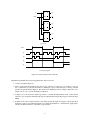
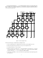
Consider the circuit shown in Figure 9. It uses a three-bit wide 5-to-1 multiplexer to enable the selection of five
characters that are displayed on a 7-segment display. Using the 7-segment decoder from Part IV this circuit can
display any of the characters H, E, L, O, and ‘blank’. The character codes are set according to Table 1 by using
the switches SW14−0 , and a specific character is selected for display by setting the switches SW17−15 .
An outline of the Verilog code that represents this circuit is provided in Figure 10. Note that we have used the
circuits from Parts III and IV as subcircuits in this code. You are to extend the code in Figure 10 so that it uses five
7-segment displays rather than just one. You will need to use five instances of each of the subcircuits. The purpose
of your circuit is to display any word on the five displays that is composed of the characters in Table 1, and be
able to rotate this word in a circular fashion across the displays when the switches SW17−15 are toggled. As an example, if the displayed word is HELLO, then your circuit should produce the output patterns illustrated in Table 2.
SW 17
SW 16
SW 15
SW 14 – 12
3
SW 11 – 9
3
SW 8 – 6
3
SW 5 – 3
SW 2 – 0
3
0
000
001
010
011
100
7-segment
decoder
3
7
5
6
4
2
3
3
Figure 9. A circuit that can select and display one of five characters.
7
1
module part5 (SW, HEX0);
input [17:0] SW;
// toggle switches
output [0:6] HEX0;
// 7-seg displays
wire [2:0] M;
mux_3bit_5to1 M0 (SW[17:15], SW[14:12], SW[11:9], SW[8:6], SW[5:3], SW[2:0], M);
char_7seg H0 (M, HEX0);
endmodule
// implements a 3-bit wide 5-to-1 multiplexer
module mux_3bit_5to1 (S, U, V, W, X, Y, M);
input [2:0] S, U, V, W, X, Y;
output [2:0] M;
. . . code not shown
endmodule
// implements a 7-segment decoder for H, E, L, O, and ‘blank’
module char_7seg (C, Display);
input [2:0] C;
// input code
output [0:6] Display; // output 7-seg code
. . . code not shown
endmodule
Figure 10. Verilog code for the circuit in Figure 9.
Character pattern
SW17 SW16 SW15
000
001
010
011
100
H
E
L
L
O
E
L
L
O
H
L
L
O
H
E
L
O
H
E
L
O
H
E
L
L
Table 2. Rotating the word HELLO on five displays.
Perform the following steps.
1. Create a new Quartus II project for your circuit.
2. Include your Verilog module in the Quartus II project. Connect the switches SW17−15 to the select inputs of
each of the five instances of the three-bit wide 5-to-1 multiplexers. Also connect SW14−0 to each instance
of the multiplexers as required to produce the patterns of characters shown in Table 2. Connect the outputs
of the five multiplexers to the 7-segment displays HEX4, HEX3, HEX2, HEX1, and HEX0.
3. Include the required pin assignments for the DE2-series board for all switches, LEDs, and 7-segment displays. Compile the project.
4. Download the compiled circuit into the FPGA chip. Test the functionality of the circuit by setting the proper
character codes on the switches SW14−0 and then toggling SW17−15 to observe the rotation of the characters.
8
Part VI
Extend your design from Part V so that is uses all eight 7-segment displays on the DE2 board. Your circuit should
be able to display words with five (or fewer) characters on the eight displays, and rotate the displayed word when
the switches SW17−15 are toggled. If the displayed word is HELLO, then your circuit should produce the patterns
shown in Table 3.
Character pattern
SW17 SW16 SW15
000
001
010
011
100
101
110
111
H
E
L
L
O
H
E
L
L
O
H
E
L
L
O
H
E
L
L
O
E
L
L
O
H
L
L
O
H
E
L
O
H
E
L
O
H
E
L
L
Table 3. Rotating the word HELLO on eight displays.
Perform the following steps:
1. Create a new Quartus II project for your circuit and select the appropriate target chip.
2. Include your Verilog module in the Quartus II project. Connect the switches SW17−15 to the select inputs of
each instance of the multiplexers in your circuit. Also connect SW14−0 to each instance of the multiplexers
as required to produce the patterns of characters shown in Table 3. (Hint: for some inputs of the multiplexers
you will want to select the ‘blank’ character.) Connect the outputs of your multiplexers to the 7-segment
displays HEX7, . . ., HEX0.
3. Include the required pin assignments for the DE2-series board for all switches, LEDs, and 7-segment displays. Compile the project.
4. Download the compiled circuit into the FPGA chip. Test the functionality of the circuit by setting the proper
character codes on the switches SW14−0 and then toggling SW17−15 to observe the rotation of the characters.
c
Copyright 2011
Altera Corporation.
9
Laboratory Exercise 2
Numbers and Displays
This is an exercise in designing combinational circuits that can perform binary-to-decimal number conversion
and binary-coded-decimal (BCD) addition.
Part I
We wish to display on the 7-segment displays HEX3 to HEX0 the values set by the switches SW15−0 . Let the
values denoted by SW15−12 , SW11−8 , SW7−4 and SW3−0 be displayed on HEX3, HEX2, HEX1 and HEX0,
respectively. Your circuit should be able to display the digits from 0 to 9, and should treat the valuations 1010 to
1111 as don’t-cares.
1. Create a new project which will be used to implement the desired circuit on the Altera DE2-series board.
The intent of this exercise is to manually derive the logic functions needed for the 7-segment displays. You
should use only simple Verilog assign statements in your code and specify each logic function as a Boolean
expression.
2. Write a Verilog file that provides the necessary functionality. Include this file in your project and assign
the pins on the FPGA to connect to the switches and 7-segment displays, as indicated in the User Manual
for the DE2-series board. The procedure for making pin assignments is described in the tutorial Quartus II
Introduction using Verilog Design, which is available on the DE2-Series System CD and in the University
Program section of Altera’s web site.
3. Compile the project and download the compiled circuit into the FPGA chip.
4. Test the functionality of your design by toggling the switches and observing the displays.
Part II
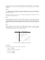
You are to design a circuit that converts a four-bit binary number V = v3 v2 v1 v0 into its two-digit decimal equivalent D = d1 d0 . Table 1 shows the required output values. A partial design of this circuit is given in Figure 1. It
includes a comparator that checks when the value of V is greater than 9, and uses the output of this comparator in
the control of the 7-segment displays. You are to complete the design of this circuit by creating a Verilog module
which includes the comparator, multiplexers, and circuit A (do not include circuit B or the 7-segment decoder at
this point). Your Verilog module should have the four-bit input V , the four-bit output M and the output z. The
intent of this exercise is to use simple Verilog assign statements to specify the required logic functions using
Boolean expressions. Your Verilog code should not include any if-else, case, or similar statements.
Binary value
Decimal digits
0000
0001
0010
...
0
0
0
...
0
1
2
...
1001
1010
1011
1100
1101
1110
1111
0
1
1
1
1
1
1
9
0
1
2
3
4
5
Table 1. Binary-to-decimal conversion values.
1
Perform the following steps:
1. Make a Quartus II project for your Verilog module.
2. Compile the circuit and use functional simulation to verify the correct operation of your comparator, multiplexers, and circuit A.
3. Augment your Verilog code to include circuit B in Figure 1 as well as the 7-segment decoder. Change the
inputs and outputs of your code to use switches SW3−0 on the DE2-series board to represent the binary
number V , and the displays HEX1 and HEX0 to show the values of decimal digits d1 and d0 . Make sure to
include in your project the required pin assignments for the DE2-series board.
4. Recompile the project, and then download the circuit into the FPGA chip.
5. Test your circuit by trying all possible values of V and observing the output displays.
d1
z
0
Comparator
Circuit B
v3
5
6
4
m3
0
0
7
1
2
3
1
d0
v2
m2
0
0
1
7-segment
decoder
v1
7
0
v0
1
m1
0
m0
5
6
4
1
2
3
1
Circuit A
Figure 1: Partial design of the binary-to-decimal conversion circuit.
Part III
Figure 2a shows a circuit for a full adder, which has the inputs a, b, and ci , and produces the outputs s and co .
Parts b and c of the figure show a circuit symbol and truth table for the full adder, which produces the two-bit
binary sum co s = a + b + ci . Figure 2d shows how four instances of this full adder module can be used to design
a circuit that adds two four-bit numbers. This type of circuit is usually called a ripple-carry adder, because of
the way that the carry signals are passed from one full adder to the next. Write Verilog code that implements this
circuit, as described below.
2
ci
s
a
ci
s
a
b
0
a) Full adder circuit
b a ci
0
0
0
0
1
1
1
1
0
0
1
1
0
0
1
1
0
1
0
1
0
1
0
1
co s
0
0
0
1
0
1
1
1
0
1
1
0
1
0
0
1
c) Full adder truth table
co
b
co
1
FA
b) Full adder symbol
b3 a3 c
3
b2 a2 c
2
FA
b1 a1 c
1
FA
c out s 3
FA
s2
b 0 a 0 c in
FA
s1
s0
d) Four-bit ripple-carry adder circuit
Figure 2: A ripple-carry adder circuit.
1. Create a new Quartus II project for the adder circuit. Write a Verilog module for the full adder subcircuit
and write a top-level Verilog module that instantiates four instances of this full adder.
2. Use switches SW7−4 and SW3−0 to represent the inputs A and B, respectively. Use SW8 for the carry-in
cin of the adder. Connect the SW switches to their corresponding red lights LEDR, and connect the outputs
of the adder, cout and S, to the green lights LEDG.
3. Include the necessary pin assignments for the DE2-series board, compile the circuit, and download it into
the FPGA chip.
4. Test your circuit by trying different values for numbers A, B, and cin .
Part IV
In part II we discussed the conversion of binary numbers into decimal digits. It is sometimes useful to build
circuits that use this method of representing decimal numbers, in which each decimal digit is represented using
four bits. This scheme is known as the binary coded decimal (BCD) representation. As an example, the decimal
value 59 is encoded in BCD form as 0101 1001.
You are to design a circuit that adds two BCD digits. The inputs to the circuit are BCD numbers A and B,
plus a carry-in, cin . The output should be a two-digit BCD sum S1 S0 . Note that the largest sum that needs to be
handled by this circuit is S1 S0 = 9 + 9 + 1 = 19. Perform the steps given below.
1. Create a new Quartus II project for your BCD adder. You should use the four-bit adder circuit from part III
to produce a four-bit sum and carry-out for the operation A + B. A circuit that converts this five-bit result,
which has the maximum value 19, into two BCD digits S1 S0 can be designed in a very similar way as the
binary-to-decimal converter from part II. Write your Verilog code using simple assign statements to specify
the required logic functions–do not use other types of Verilog statements such as if-else or case statements
for this part of the exercise.
3
2. Use switches SW7−4 and SW3−0 for the inputs A and B, respectively, and use SW8 for the carry-in.
Connect the SW switches to their corresponding red lights LEDR, and connect the four-bit sum and carryout produced by the operation A + B to the green lights LEDG. Display the BCD values of A and B on the
7-segment displays HEX6 and HEX4, and display the result S1 S0 on HEX1 and HEX0.
3. Since your circuit handles only BCD digits, check for the cases when the input A or B is greater than nine.
If this occurs, indicate an error by turning on the green light LEDG8 .
4. Include the necessary pin assignments for the DE2-series board, compile the circuit, and download it into
the FPGA chip.
5. Test your circuit by trying different values for numbers A, B, and cin .
Part V
Design a circuit that can add two 2-digit BCD numbers, A1 A0 and B1 B0 to produce the three-digit BCD sum
S2 S1 S0 . Use two instances of your circuit from part IV to build this two-digit BCD adder. Perform the steps
below:
1. Use switches SW15−8 and SW7−0 to represent 2-digit BCD numbers A1 A0 and B1 B0 , respectively. The
value of A1 A0 should be displayed on the 7-segment displays HEX7 and HEX6, while B1 B0 should be on
HEX5 and HEX4. Display the BCD sum, S2 S1 S0 , on the 7-segment displays HEX2, HEX1 and HEX0.
2. Make the necessary pin assignments and compile the circuit.
3. Download the circuit into the FPGA chip, and test its operation.
Part VI
In part V you created Verilog code for a two-digit BCD adder by using two instances of the Verilog code for a
one-digit BCD adder from part IV. A different approach for describing the two-digit BCD adder in Verilog code
is to specify an algorithm like the one represented by the following pseudo-code:
1
2
3
4
5
6
7
8
9
T0 = A0 + B0
if (T0 > 9) then
Z0 = 10;
c1 = 1;
else
Z0 = 0;
c1 = 0;
end if
S0 = T0 − Z0
10
11
12
13
14
15
16
17
18
19
T1 = A1 + B1 + c1
if (T1 > 9) then
Z1 = 10;
c2 = 1;
else
Z1 = 0;
c2 = 0;
end if
S1 = T1 − Z1
S2 = c2
4
It is reasonably straightforward to see what circuit could be used to implement this pseudo-code. Lines 1, 9, 10,
and 18 represent adders, lines 2-8 and 11-17 correspond to multiplexers, and testing for the conditions T0 > 9
and T1 > 9 requires comparators. You are to write Verilog code that corresponds to this pseudo-code. Note that
you can perform addition operations in your Verilog code instead of the subtractions shown in lines 9 and 18. The
intent of this part of the exercise is to examine the effects of relying more on the Verilog compiler to design the
circuit by using if-else statements along with the Verilog > and + operators. Perform the following steps:
1. Create a new Quartus II project for your Verilog code. Use the same switches, lights, and displays as in
part V. Compile your circuit.
2. Use the Quartus II RTL Viewer tool to examine the circuit produced by compiling your Verilog code.
Compare the circuit to the one you designed in Part V.
3. Download your circuit onto the DE2-series board and test it by trying different values for numbers A1 A0
and B1 B0 .
Part VII
Design a combinational circuit that converts a 6-bit binary number into a 2-digit decimal number represented in
the BCD form. Use switches SW5−0 to input the binary number and 7-segment displays HEX1 and HEX0 to
display the decimal number. Implement your circuit on the DE2-series board and demonstrate its functionality.
c
Copyright 2011
Altera Corporation.
5
Laboratory Exercise 3
Latches, Flip-flops, and Registers
The purpose of this exercise is to investigate latches, flip-flops, and registers.
Part I
Altera FPGAs include flip-flops that are available for implementing a user’s circuit. We will show how to make
use of these flip-flops in Part IV of this exercise. But first we will show how storage elements can be created in an
FPGA without using its dedicated flip-flops.
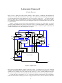
Figure 1 depicts a gated RS latch circuit. Two styles of Verilog code that can be used to describe this circuit
are given in Figure 2. Part a of the figure specifies the latch by instantiating logic gates, and part b uses logic
expressions to create the same circuit. If this latch is implemented in an FPGA that has 4-input lookup tables
(LUTs), then only one lookup table is needed, as shown in Figure 3a.
R_g
R
Qa (Q)
Clk
Qb
S_g
S
Figure 1: A gated RS latch circuit.
// A gated RS latch
module part1 (Clk, R, S, Q);
input Clk, R, S;
output Q;
wire R_g, S_g, Qa, Qb /* synthesis keep */ ;
and (R_g, R, Clk);
and (S_g, S, Clk);
nor (Qa, R_g, Qb);
nor (Qb, S_g, Qa);
assign Q = Qa;
endmodule
Figure 2a. Instantiating logic gates for the RS latch.
1
// A gated RS latch
module part1 (Clk, R, S, Q);
input Clk, R, S;
output Q;
wire R_g, S_g, Qa, Qb /* synthesis keep */ ;
assign R_g = R & Clk;
assign S_g = S & Clk;
assign Qa = ∼(R_g | Qb);
assign Qb = ∼(S_g | Qa);
assign Q = Qa;
endmodule
Figure 2b. Specifying the RS latch by using logic expressions.
Although the latch can be correctly realized in one 4-input LUT, this implementation does not allow its internal signals, such as R_g and S_g, to be observed, because they are not provided as outputs from the LUT. To
preserve these internal signals in the implemented circuit, it is necessary to include a compiler directive in the
code. In Figure 2 the directive /* synthesis keep */ is included to instruct the Quartus II compiler to use separate
logic elements for each of the signals R_g, S_g, Qa, and Qb. Compiling the code produces the circuit with four
4-LUTs depicted in Figure 3b.
R
Clk
S
Qa (Q)
4-LUT
(a) Using one 4-input lookup table for the RS latch.
R
R_g
Qa (Q)
4-LUT
4-LUT
Clk
S_g
S
4-LUT
4-LUT
Qb
(b) Using four 4-input lookup tables for the RS latch.
Figure 3. Implementation of the RS latch from Figure 1.
Create a Quartus II project for the RS latch circuit as follows:
2
1. Create a new project for the RS latch. Select the target chip as Cyclone II EP2C35F672C6 if using the
Altera DE2 board. Select the target chip as Cyclone II EP2C70F896C6 if using the Altera DE2-70 board.
Or, select the target chip as Cyclone IV EP4CE115F29C7 if using the Altera DE2-115 board.
2. Generate a Verilog file with the code in either part a or b of Figure 2 (both versions of the code should
produce the same circuit) and include it in the project.
3. Compile the code. Use the Quartus II RTL Viewer tool to examine the gate-level circuit produced from the
code, and use the Technology Viewer tool to verify that the latch is implemented as shown in Figure 3b.
4. In QSim, create a Vector Waveform File (.vwf) which specifies the inputs and outputs of the circuit. Draw
waveforms for the R and S inputs and use QSim to produce the corresponding waveforms for R_g, S_g, Qa,
and Qb. Verify that the latch works as expected using both functional and timing simulation.
Part II
Figure 4 shows the circuit for a gated D latch.
D
S
S_g
Qa (Q)
Clk
Qb
R
R_g
Figure 4. Circuit for a gated D latch.
Perform the following steps:
1. Create a new Quartus II project. Generate a Verilog file using the style of code in Figure 2b for the gated D
latch. Use the /* synthesis keep */ directive to ensure that separate logic elements are used to implement the
signals R, S_g, R_g, Qa, and Qb.
2. Select the appropriate target chip and compile the code. Use the Technology Viewer tool to examine the
implemented circuit.
3. Verify that the latch works properly for all input conditions by using functional simulation. Examine the
timing characteristics of the circuit by using timing simulation.
4. Create a new Quartus II project which will be used for implementation of the gated D latch on the DE2series board. This project should consist of a top-level module that contains the appropriate input and output
ports (pins) for the DE2-series board. Instantiate your latch in this top-level module. Use switch SW0 to
drive the D input of the latch, and use SW1 as the Clk input. Connect the Q output to LEDR0 .
5. Recompile your project and download the compiled circuit onto the DE2-series board.
6. Test the functionality of your circuit by toggling the D and Clk switches and observing the Q output.
3
Part III
Figure 5 shows the circuit for a master-slave D flip-flop.
Master
D
Clock
D
Q
Slave
Qm
Clk Q
D
Q
Clk Q
Qs
Q
Q
Figure 5. Circuit for a master-slave D flip-flop.
Perform the following:
1. Create a new Quartus II project. Generate a Verilog file that instantiates two copies of your gated D latch
module from Part II to implement the master-slave flip-flop.
2. Include in your project the appropriate input and output ports for the Altera DE2-series board. Use switch
SW0 to drive the D input of the flip-flop, and use SW1 as the Clock input. Connect the Q output to LEDR0 .
3. Compile your project.
4. Use the Technology Viewer to examine the D flip-flop circuit, and use simulation to verify its correct operation.
5. Download the circuit onto the DE2-series board and test its functionality by toggling the D and Clock
switches and observing the Q output.
Part IV
Figure 6 shows a circuit with three different storage elements: a gated D latch, a positive-edge triggered D flipflop, and a negative-edge triggered D flip-flop.
4
D
Clock
Q
Qa
Clk Q
Qa
Q
Qb
Q
Qb
Q
Qc
Q
Qc
D
D
D
(a) Circuit
Clock
D
Qa
Qb
Qc
(b) Timing diagram
Figure 6. Circuit and waveforms for Part IV.
Implement and simulate this circuit using Quartus II software as follows:
1. Create a new Quartus II project.
2. Write a Verilog file that instantiates the three storage elements. For this part you should no longer use
the /* synthesis keep */ directive from Parts I to III. Figure 7 gives a behavioral style of Verilog code that
specifies the gated D latch in Figure 4. This latch can be implemented in one 4-input lookup table. Use a
similar style of code to specify the flip-flops in Figure 6.
3. Compile your code and use the Technology Viewer to examine the implemented circuit. Verify that the
latch uses one lookup table and that the flip-flops are implemented using the flip-flops provided in the target
FPGA.
4. In QSim, create a Vector Waveform File (.vwf) which specifies the inputs and outputs of the circuit. Draw
the inputs D and Clock as indicated in Figure 6. Use functional simulation to obtain the three output signals.
Observe the different behavior of the three storage elements.
5
module D_latch (D, Clk, Q);
input D, Clk;
output reg Q;
always @ (D, Clk)
if (Clk)
Q = D;
endmodule
Figure 7. A behavioral style of Verilog code that specifies a gated D latch.
Part V
We wish to display the hexadecimal value of a 16-bit number A on the four 7-segment displays, HEX7 − 4. We
also wish to display the hex value of a 16-bit number B on the four 7-segment displays, HEX3 − 0. The values
of A and B are inputs to the circuit which are provided by means of switches SW15−0 . This is to be done by first
setting the switches to the value of A and then setting the switches to the value of B; therefore, the value of A
must be stored in the circuit.
1. Create a new Quartus II project which will be used to implement the desired circuit on the Altera DE2-series
board.
2. Write a Verilog file that provides the necessary functionality. Use KEY0 as an active-low asynchronous
reset, and use KEY1 as a clock input.
3. Include the Verilog file in your project and compile the circuit.
4. Assign the pins on the FPGA to connect to the switches and 7-segment displays, as indicated in the User
Manual for the DE2-series board.
5. Recompile the circuit and download it into the FPGA chip.
6. Test the functionality of your design by toggling the switches and observing the output displays.
c
Copyright 2011
Altera Corporation.
6
Laboratory Exercise 4
Counters
The purpose of this exercise is to build and use counters. The designed circuits are to be implemented on an
Altera DE2-series Board.
Students are expected to have a basic understanding of counters and sufficient familiarity with Verilog hardware
description language to implement various types of flip-flops.
Part I
Consider the circuit in Figure 1. It is a 4-bit synchronous counter which uses four T-type flip-flops. The counter
increments its value on each positive edge of the clock if the Enable signal is asserted. The counter is reset to 0 by
setting the Clear signal low. You are to implement a 8-bit counter of this type.
Enable
Clock
T
Q
Q
T
Q
T
Q
Q
Q
T
Q
Q
Clear
Figure 1: A 4-bit counter.
1. Write a Verilog file that defines a 8-bit counter by using the structure depicted in Figure 1. Your code should
include a T flip-flop module that is instantiated 8 times to create the counter. Compile the circuit. How
many logic elements (LEs) are used to implement your circuit? What is the maximum frequency, Fmax , at
which your circuit can be operated?
2. Simulate your circuit to verify its correctness.
3. Augment your Verilog file to use the pushbutton KEY0 as the Clock input, switches SW1 and SW0 as
Enable and Clear inputs, and 7-segment displays HEX1-0 to display the hexadecimal count as your circuit
operates. Make the necessary pin assignments needed to implement the circuit on the DE2-series board, and
compile the circuit.
4. Download your circuit into the FPGA chip and test its functionality by operating the implemented switches.
5. Implement a 4-bit version of your circuit and use the Quartus II RTL Viewer to see how Quartus II software
synthesized your circuit. What are the differences in comparison with Figure 1?
Part II
Another way to specify a counter is by using a register and adding 1 to its value. This can be accomplished using
the following Verilog statement:
Q <= Q + 1;
1
Compile a 16-bit version of this counter and determine the number of LEs needed and the Fmax that is attainable.
Use the RTL Viewer to see the structure of this implementation and comment on the differences with the design
from Part I.
Part III
Use an LPM from the Library of Parameterized modules to implement a 16-bit counter. Choose the LPM options
to be consistent with the above design, i.e. with enable and synchronous clear. How does this version compare
with the previous designs?
Note: The tutorial Using the Library of Parameterized Modules (LPM) explains the use of LPMs. It can be found
on the Altera University Program website.
Part IV
Design and implement a circuit that successively flashes digits 0 through 9 on the 7-segment display HEX0. Each
digit should be displayed for about one second. Use a counter to determine the one second intervals. The counter
should be incremented by the 50-MHz clock signal provided on the DE2-series board. Do not derive any other
clock signals in your design–make sure that all flip-flops in your circuit are clocked directly by the 50-MHz clock
signal.
Part V
Design and implement a circuit that displays the word HELLO, in ticker-tape fashion, on the eight 7-segment
displays HEX7-0. Make the letters move from right to left in intervals of about one second. The patterns that
should be displayed in successive clock intervals are given in Table 1.
Displayed pattern
Clock cycle
0
1
2
3
4
5
6
7
8
...
H
E
L
L
O
H
E
L
L
O
H
E
L
L
O
H
E
L
L
O
H
E
L
L
O
H
E
L
L
O
H
E
L
L
O
H
E
L
L
O
H
E
L
L
O
and so on
Table 1. Scrolling the word HELLO in ticker-tape fashion.
Preparation
The recommended preparation for this laboratory exercise includes:
1. Verilog code for Part I
2. Simulation of the Verilog code for Part I
3. Verilog code for Part II
4. Verilog code for Part III
2
In addition, a module that displays a hex digit on seven segment display the students designed in a previous lab
would be an asset.
c
Copyright 2011
Altera Corporation.
3
Laboratory Exercise 5
Timers and Real-time Clock
The purpose of this exercise is to study the use of clocks in timed circuits. The designed circuits are to be
implemented on an Altera DE2-series board.
Background
In Verilog hardware description language we can describe a variable-size counter by using a parameter declaration.
An example of an n-bit counter is shown in Figure 1.
module counter(clock, reset_n, Q);
parameter n = 4;
input clock, reset_n;
output [n-1:0] Q;
reg
[n-1:0] Q;
always @(posedge clock or negedge reset_n)
begin
if (˜reset_n)
Q <= ’d0;
else
Q <= Q + 1’b1;
end
endmodule
Figure 1: A Verilog description of an n-bit counter.
The parameter n specifies the number of bits in the counter. A particular value of this parameter is defined by
using a defparam statement. For example, an 8-bit counter can be specified as:
counter eight_bit(clock, reset_n, Q);
defparam eight_bit.N = 8;
By using parameters we can instantiate counters of different sizes in a logic circuit, without having to create a new
module for each counter.
Part I
Create a modulo-k counter by modifying the design of an 8-bit counter to contain an additional parameter. The
counter should count from 0 to k − 1. When the counter reaches the value k − 1 the value that follows should be
0.
Your circuit should use pushbutton KEY0 as an asynchronous reset, KEY1 as a manual clock input. The contents
of the counter should be displayed on red LEDs. Compile your design with Quartus II software, download your
design onto a DE2-series board, and test its operation. Perform the following steps:
1. Create a new Quartus II project which will be used to implement the desired circuit on the DE2-series board.
1
2. Write a Verilog file that specifies the desired circuit.
3. Include the Verilog file in your project and compile the circuit.
4. Simulate the designed circuit to verify its functionality.
5. Assign the pins on the FPGA to connect to the lights and pushbutton switches, by importing the appropriate
pin assignment file.
6. Recompile the circuit and download it into the FPGA chip.
7. Verify that your circuit works correctly by observing the display.
Part II
Implement a 3-digit BCD counter. Display the contents of the counter on the 7-segment displays, HEX2−0. Derive
a control signal, from the 50-MHz clock signal provided on the DE2-series board, to increment the contents of the
counter at one-second intervals. Use the pushbutton switch KEY0 to reset the counter to 0.
Part III
Design and implement a circuit on the DE2-series board that acts as a time-of-day clock. It should display the
hour (from 0 to 23) on the 7-segment displays HEX7−6, the minute (from 0 to 60) on HEX5−4 and the second
(from 0 to 60) on HEX3−2. Use the switches SW15−0 to preset the hour and minute parts of the time displayed by
the clock.
Part IV
An early method of telegraph communication was based on the Morse code. This code uses patterns of short and
long pulses to represent a message. Each letter is represented as a sequence of dots (a short pulse), and dashes (a
long pulse). For example, the first eight letters of the alphabet have the following representation:
A
B
C
D
E
F
G
H
•—
—•••
—•—•
—••
•
••—•
——•
••••
Design and implement a circuit that takes as input one of the first eight letters of the alphabet and displays the
Morse code for it on a red LED. Your circuit should use switches SW2−0 and pushbuttons KEY1−0 as inputs. When
a user presses KEY1 , the circuit should display the Morse code for a letter specified by SW2−0 (000 for A, 001 for
B, etc.), using 0.5-second pulses to represent dots, and 1.5-second pulses to represent dashes. Pushbutton KEY0
should function as an asynchronous reset. A high-level schematic diagram of the circuit is shown in Figure 2.
Hint: Use a counter to generate 0.5-second pulses, and another counter to keep the LEDR0 light on for either
0.5 or 1.5 seconds.
2
Pushbuttons and switches
Letter size register
Data
Enable
Load
Letter
Selection
Logic
Logic
Letter symbols shift register
Data
Enable
Load
2-bit counter
Reset
Enable
Figure 2: High-level schematic diagram of the circuit for part IV.
Preparation
The recommended preparation for this laboratory exercise includes:
1. Verilog code for Part I
2. Simulation of the Verilog code for Part I
3. Verilog code for Part II
4. Verilog code for Part III
c
Copyright 2011
Altera Corporation.
3
LEDR0
Laboratory Exercise 6
ci
Adders, Subtractors, and Multipliers
s
a
ci
s
a
The purpose of this exercise is to examine arithmetic circuitsFA
that add, subtract,
and multiply numbers. Each
c
b
b on an Altera DE2-serieso board.
circuit will be described in0 Verilog and implemented
c
o
1
Part I
a) Full adder circuit
b) Full adder symbol
Consider again the four-bit ripple-carry adder circuit used in lab exercise 2; its diagram is reproduced in Figure 1.
b a ci
0
0
0
0
1
1
1
1
0
0
1
1
0
0
1
1
0
1
0
1
0
1
0
1
co s
0
0
0
1
0
1
1
1
0
1
1
0
1
0
0
1
c) Full adder truth table
b3 a3 c
3
FA
c out s 3
b2 a2 c
2
b1 a1 c
1
FA
FA
s2
b 0 a 0 c in
FA
s1
s0
d) Four-bit ripple-carry adder circuit
Figure 1: A four-bit ripple carry adder.
This circuit can be implemented using a ’+’ sign in Verilog. For example, the following code fragment adds n-bit
numbers A and B to produce outputs sum and carry:
wire [n-1:0] sum;
wire carry;
...
assign {carry, sum} = A + B;
Use this construct to implement a circuit shown in Figure 2.
Design and compile your circuit with Quartus II software, download it onto a DE2-series board, and test its
operation as follows:
1. Create a new Quartus II project. Select the appropriate target chip that matches the FPGA chip on the Altera
DE2-series board. Implement the designed circuit on the DE2-series board.
2. Write Verilog code that describes the circuit in Figure 2.
3. Connect input A to switches SW7−0 , and use KEY0 as an active-low asynchronous reset and KEY1 as a
manual clock input. The sum output should be displayed on red LEDR7−0 lights and the carry-out should
be displayed on the red LEDR8 light.
4. Assign the pins on the FPGA to connect to the switches and 7-segment displays by importing the appropriate
pin assignment file.
5. Compile your design and use timing simulation to verify the correct operation of the circuit. Once the
simulation works properly, download the circuit onto the DE2-series board and test it by using different
values of A. Be sure to check that the Overflow output works correctly.
1
b3 a3 c
3
b2 a2 c
2
FA
b1 a1 c
1
FA
b 0 a 0 c in
FA
FA
6. Open the Quartus II Compilation Report and examine the results reported by the Timing Analyzer. What is
s 1 What is the slongest
the maximum operationcfrequency,
fmax , sof2 your circuit?
path in the circuit in terms of
out s 3
0
delay?
a) Four-bit ripple-carry adder circuit
A
8
R
Clock
Q
8
overflow
Q D
c in
+
0
8
R
Q
Overflow
S
b) Eight-bit
registeredaccumulator
adder circuit circuit.
Figure
2: An eight-bit
Part II
Extend the circuit from Part I to be able to both add and subtract numbers. To do so, add an add sub input to your
circuit. When add sub is 1, your circuit should subtract A from S, and add A and S as in Part I otherwise.
Part III
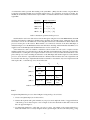
Figure 3a gives an example of paper-and-pencil multiplication P = A × B, where A = 11 and B = 12.
x
1 1
x 1 2
2 2
1 1
1 3 2
1
x 1
0
0 0
1 0 1
1 0 1 1
0 1 1
1 0 0
a) Decimal
a2
b2
a1
b1
a0
b0
a3 b0 a2 b0 a1 b0 a0 b0
a3 b1 a2 b1 a1 b1 a0 b1
0 0 0
0 0
1
1 0 0 0 0 1 0 0
a3
b3
a3 b2 a2 b2 a1 b2 a0 b2
a3 b3 a2 b3 a1 b3 a0 b3
p7
b) Binary
p6
p5
p4
p3
p2
p1
p0
c) Implementation
Figure 3: Multiplication of binary numbers.
We compute P = A × B as an addition of summands. The first summand is equal to A times the ones digit of B.
The second summand is A times the tens digit of B, shifted one position to the left. We add the two summands to
form the product P = 132.
Part b of the figure shows the same example using four-bit binary numbers. To compute P = A × B, we first
form summands by multiplying A by each digit of B. Since each digit of B is either 1 or 0, the summands are
either shifted versions of A or 0000. Figure 3c shows how each summand can be formed by using the Boolean
AND operation of A with the appropriate bit of B.
2
A four-bit circuit that implements P = A × B is illustrated in Figure 4. Because of its regular structure, this
type of multiplier circuit is called an array multiplier. The shaded areas correspond to the shaded columns in
Figure 3c. In each row of the multiplier AND gates are used to produce the summands, and full adder modules are
used to generate the required sums.
a3
a2
a3
a1
a2
a0
a1
a0
b0
b1
0
b
a
c o FA c i
b
a
c o FA c i
b
a
c o FA c i
b
a
c o FA c i
s
s
s
s
a2
a3
a1
0
a0
b2
a3
b
a
c o FA c i
b
a
c o FA c i
b
a
c o FA c i
b
a
c o FA c i
s
s
s
s
a2
a1
0
a0
b3
p7
b
a
c o FA c i
b
a
c o FA c i
b
a
c o FA c i
b
a
c o FA c i
s
s
s
s
p6
p5
p4
p3
0
p2
p1
p0
Figure 4: An array multiplier circuit.
Perform the following steps to implement the array multiplier circuit:
1. Create a new Quartus II project to implement the desired circuit on the Altera DE2-series board.
2. Generate the required Verilog file, include it in your project, and compile the circuit.
3. Use functional simulation to verify your design.
4. Augment your design to use switches SW11−8 to represent the number A and switches SW3−0 to represent
B. The hexadecimal values of A and B are to be displayed on the 7-segment displays HEX6 and HEX4,
respectively. The result P = A × B is to be displayed on HEX1 and HEX0.
5. Assign the pins on the FPGA to connect to the switches and 7-segment displays by importing the appropriate
pin assignment file.
3
6. Recompile the circuit and download it into the FPGA chip.
7. Test the functionality of your circuit by toggling the switches and observing the 7-segment displays.
Part IV
In Part III, an array multiplier was implemented using full adder modules. At a higher level, a row of full adders
functions as an n-bit adder and the array multiplier circuit can be represented as shown in Figure 5.
a3
a2
a1
a0
b0
a3
a0
a1
a2
b1
0
b3
co
a3
b2
s3
a3
a2
a2
b1 a1
n-bit Adder
s2
s1
a1
b0 a0
ci
s0
0
a0
b2
b3 a3
co
s3
a3
a2
b2
a2
b1 a1
n-bit Adder
s2
s1
a1
b0 a0
ci
s0
0
a0
b3
b3 a3
co
s3
p7
p6
b2
a2
b1 a1
n-bit Adder
s2
s1
p5
p4
b0 a0
ci
s0
p3
0
p2
p1
p0
Figure 5: An array multiplier implemented using n-bit adders.
Each n-bit adder adds a shifted version of A for a given row and the partial sum of the row above. Abstracting the
multiplier circuit as a sequence of additions allows us to build larger multipliers. The multiplier should consist of
n-bit adders arranged in a structure shown in Figure 5. Use this approach to implement an 8x8 multiplier circuit
with registered inputs and outputs, as shown in Figure 6.
4
A
B
5
Clock
5
D
D
Q
Q
Multiplier
10
D
R
Q
P
Figure 6: A registered multiplier circuit.
Perform the following steps:
1. Create a new Quartus II project.
2. Write the required Verilog file, include it in your project, and compile the circuit.
3. Use functional simulation to verify your design.
4. Augment your design to use switches SW15−8 to represent the number A and switches SW7−0 to represent
B. The hexadecimal values of A and B are to be displayed on the 7-segment displays HEX7-6 and HEX5-4,
respectively. The result P = A × B is to be displayed on HEX3-0.
5. Assign the pins on the FPGA to connect to the switches and 7-segment displays.
6. Recompile the circuit and download it into the FPGA chip.
7. Test the functionality of your design by toggling the switches and observing the 7-segment displays.
8. How large is the circuit in terms of the number of logic elements?
9. What is the fmax for this circuit?
Part V
Part IV showed how to implement multiplication A × B as a sequence of additions, by accumulating the shifted
versions of A one row at a time. Another way to implement this circuit is to perform addition using an adder tree.
An adder tree is a method of adding several numbers together in a parallel fashion. This idea is illustrated in
Figure 7. In the figure, numbers A, B, C, D, E, F , G, and H are added together in parallel. The addition A + B
happens simultaneously with C + D, E + F and G + H. The result of these operations are then added in parallel
again, until the final sum P is computed.
5
A
B
C
+
D
E
+
F
G
+
+
H
+
+
+
P
Figure 7: An example of adding 8 numbers using an adder tree.
In this part you are to implement an 8x8 array multiplier that computes P = A×B. Use an adder tree structure
to implement operations shown in Figure 5. Inputs A and B, as well as the output P should be registered as in
Part IV. What is the fmax for this circuit?
Preparation
The recommended preparation for this laboratory exercise includes Verilog code for Parts I through V.
c
Copyright 2011
Altera Corporation.
6
Laboratory Exercise 7
Finite State Machines
This is an exercise in using finite state machines.
Part I
We wish to implement a finite state machine (FSM) that recognizes two specific sequences of applied input symbols, namely four consecutive 1s or four consecutive 0s. There is an input w and an output z. Whenever w = 1 or
w = 0 for four consecutive clock pulses the value of z has to be 1; otherwise, z = 0. Overlapping sequences are
allowed, so that if w = 1 for five consecutive clock pulses the output z will be equal to 1 after the fourth and fifth
pulses. Figure 1 illustrates the required relationship between w and z.
Clock
w
z
Figure 1: Required timing for the output z.
A state diagram for this FSM is shown in Figure 2. For this part you are to manually derive an FSM circuit that
implements this state diagram, including the logic expressions that feed each of the state flip-flops. To implement
the FSM use nine state flip-flops called y8 , . . . , y0 and the one-hot state assignment given in Table 1.
Reset
A/0
w=0
w=1
1
B/0
F/0
0
w=0
1
1
0
G/0
C/0
w=0
D/0
1
0
1
0
w=0
0
1
H/0
1
E/1
I/1
Figure 2: A state diagram for the FSM.
1
1
Name
State Code
y8 y7 y6 y5 y4 y3 y2 y1 y0
A
B
C
D
E
F
G
H
I
000000001
000000010
000000100
000001000
000010000
000100000
001000000
010000000
100000000
Table 1: One-hot codes for the FSM.
Design and implement your circuit on the DE2-series board as follows:
1. Create a new Quartus II project for the FSM circuit. Select the appropriate target chip that matches the
FPGA chip on the Altera DE2-series board.
2. Write a Verilog file that instantiates the nine flip-flops in the circuit and which specifies the logic expressions
that drive the flip-flop input ports. Use only simple assign statements in your Verilog code to specify the
logic feeding the flip-flops. Note that the one-hot code enables you to derive these expressions by inspection.
Use the toggle switch SW0 on the DE2-series board as an active-low synchronous reset input for the FSM,
use SW1 as the w input, and the pushbutton KEY0 as the clock input which is applied manually. Use the
green light LEDG0 as the output z, and assign the state flip-flop outputs to the red lights LEDR8 to LEDR0 .
3. Include the Verilog file in your project, and assign the pins on the FPGA to connect to the switches and the
LEDs, as indicated in the User Manual for the DE2-series board. Compile the circuit.
4. Simulate the behavior of your circuit.
5. Once you are confident that the circuit works properly as a result of your simulation, download the circuit
into the FPGA chip. Test the functionality of your design by applying the input sequences and observing
the output LEDs. Make sure that the FSM properly transitions between states as displayed on the red LEDs,
and that it produces the correct output values on LEDG0 .
6. Finally, consider a modification of the one-hot code given in Table 1. When an FSM is going to be implemented in an FPGA, the circuit can often be simplified if all flip-flop outputs are 0 when the FSM is in the
reset state. This approach is preferable because the FPGA’s flip-flops usually include a clear input, which
can be conveniently used to realize the reset state, but the flip-flops often do not include a set input.
Table 2 shows a modified one-hot state assignment in which the reset state, A, uses all 0s. This is accomplished by inverting the state variable y0 . Create a modified version of your Verilog code that implements
this state assignment. (Hint: you should need to make very few changes to the logic expressions in your
circuit to implement the modified state assignment.) Compile your new circuit and test it both through
simulation and by downloading it onto the DE2-series board.
2
Name
State Code
y8 y7 y6 y5 y4 y3 y2 y1 y0
A
B
C
D
E
F
G
H
I
000000000
000000011
000000101
000001001
000010001
000100001
001000001
010000001
100000001
Table 2: Modified one-hot codes for the FSM.
Part II
For this part you are to write another style of Verilog code for the FSM in Figure 2. In this version of the code you
should not manually derive the logic expressions needed for each state flip-flop. Instead, describe the state table
for the FSM by using a Verilog case statement in an always block, and use another always block to instantiate
the state flip-flops. You can use a third always block or simple assignment statements to specify the output z. To
implement the FSM, use four state flip-flops y3 , . . . , y0 and binary codes, as shown in Table 3.
Name
State Code
y3 y2 y1 y0
A
B
C
D
E
F
G
H
I
0000
0001
0010
0011
0100
0101
0110
0111
1000
Table 3: Binary codes for the FSM.
A suggested skeleton of the Verilog code is given in Figure 3.
3
module part2 ( . . . );
. . . define input and output ports
. . . define signals
reg [3:0] y_Q, Y_D;
// y_Q represents current state, Y_D represents next state
parameter A = 4’b0000, B = 4’b0001, C = 4’b0010, D = 4’b0011, E = 4’b0100,
F = 4’b0101, G = 4’b0110, H = 4’b0111, I = 4’b1000;
always @(w, y_Q)
begin: state_table
case (y_Q)
A: if (!w) Y_D = B;
else Y_D = F;
. . . remainder of state table
default: Y_D = 4’bxxxx;
endcase
end // state_table
always @(posedge Clock)
begin: state_FFs
...
end // state_FFS
. . . assignments for output z and the LEDs
endmodule
Figure 3: Skeleton Verilog code for the FSM.
Implement your circuit as follows.
1. Create a new project for the FSM.
2. Include in the project your Verilog file that uses the style of code in Figure 3. Use the toggle switch SW0 on
the DE2-series board as an active-low synchronous reset input for the FSM, use SW1 as the w input, and the
pushbutton KEY0 as the clock input which is applied manually. Use the green light LEDG0 as the output
z, and assign the state flip-flop outputs to the red lights LEDR3 to LEDR0 . Assign the pins on the FPGA to
connect to the switches and the LEDs, as indicated in the User Manual for the DE2-series board.
3. Before compiling your code it is necessary to explicitly tell the Synthesis tool in Quartus II that you wish to
have the finite state machine implemented using the state assignment specified in your Verilog code. If you
do not explicitly give this setting to Quartus II, the Synthesis tool will automatically use a state assignment
of its own choosing, and it will ignore the state codes specified in your Verilog code. To make this setting,
choose Assignments > Settings in Quartus II, and click on the Analysis and Synthesis item on the left
side of the window, then click on the More Setting button. As indicated in Figure 4, change the parameter
State Machine Processing to the setting User-Encoded.
4. To examine the circuit produced by Quartus II open the RTL Viewer tool. Double-click on the box shown
in the circuit that represents the finite state machine, and determine whether the state diagram that it shows
properly corresponds to the one in Figure 2. To see the state codes used for your FSM, open the Compilation
Report, select the Analysis and Synthesis section of the report, and click on State Machines.
5. Simulate the behavior of your circuit.
6. Once you are confident that the circuit works properly as a result of your simulation, download the circuit
into the FPGA chip. Test the functionality of your design by applying the input sequences and observing
4
the output LEDs. Make sure that the FSM properly transitions between states as displayed on the red LEDs,
and that it produces the correct output values on LEDG0 .
7. In step 3 you instructed the Quartus II Synthesis tool to use the state assignment given in your Verilog
code. To see the result of removing this setting, open again the Quartus II settings window by choosing
Assignments > Settings, and click on the Analysis and Synthesis item, then click on the More Setting
button. Change the setting for State Machine Processing from User-Encoded to One-Hot. Recompile
the circuit and then open the report file, select the Analysis and Synthesis section of the report, and click
on State Machines. Compare the state codes shown to those given in Table 2, and discuss any differences
that you observe.
Figure 4: Specifying the state assignment method in Quartus II.
Part III
The sequence detector can be implemented in a straightforward manner using shift registers, instead of using
the more formal approach described above. Create Verilog code that instantiates two 4-bit shift registers; one
is for recognizing a sequence of four 0s, and the other for four 1s. Include the appropriate logic expressions in
your design to produce the output z. Make a Quartus II project for your design and implement the circuit on the
DE2-series board. Use the switches and LEDs on the board in a similar way as you did for Parts I and II and
observe the behavior of your shift registers and the output z. Answer the following question: could you use just
one 4-bit shift register, rather than two? Explain your answer.
5
Part IV
In this part of the exercise you are to implement a Morse-code encoder using an FSM. The Morse code uses patterns of short and long pulses to represent a message. Each letter is represented as a sequence of dots (a short
pulse), and dashes (a long pulse). For example, the first eight letters of the alphabet have the following representation:
A
B
C
D
E
F
G
H
•—
—•••
—•—•
—••
•
••—•
——•
••••
Design and implement a Morse-code encoder circuit using an FSM. Your circuit should take as input one of
the first eight letters of the alphabet and display the Morse code for it on a red LED. Use switches SW2−0 and
pushbuttons KEY1−0 as inputs. When a user presses KEY1 , the circuit should display the Morse code for a letter
specified by SW2−0 (000 for A, 001 for B, etc.), using 0.5-second pulses to represent dots, and 1.5-second pulses
to represent dashes. Pushbutton KEY0 should function as an asynchronous reset.
A high-level schematic diagram of a possible circuit for the Morse-code encoder is shown in Figure 5.
Pushbuttons and switches
Morse code length counter
Data
Enable
Load
Letter
selection
logic
FSM
Morse code shift register
Data
Enable
Load
Half-second counter
Figure 5: High-level schematic diagram of the circuit for Part IV.
Preparation
The recommended preparation for this exercise is to write Verilog code for Parts I through IV.
c
Copyright 2011
Altera Corporation.
6
LEDR0
Laboratory Exercise 8
Memory Blocks
In computer systems it is necessary to provide a substantial amount of memory. If a system is implemented
using FPGA technology it is possible to provide some amount of memory by using the memory resources that exist
in the FPGA device. If additional memory is needed, it has to be implemented by connecting external memory
chips to the FPGA. In this exercise we will examine the general issues involved in implementing such memory.
A diagram of the random access memory (RAM) module that we will implement is shown in Figure 1a. It
contains 32 eight-bit words (rows), which are accessed using a five-bit address port, an eight-bit data port, and a
write control input. We will consider two different ways of implementing this memory: using dedicated memory
blocks in an FPGA device, and using a separate memory chip.
The Cyclone II 2C35 FPGA that is included on the DE2 board provides dedicated memory resources called
M4K blocks. Each M4K block contains 4096 memory bits, which can be configured to implement memories of
various sizes. A common term used to specify the size of a memory is its aspect ratio, which gives the depth in
words and the width in bits (depth x width). Some aspect ratios supported by the M4K block are 4K x 1, 2K x
2, 1K x 4, and 512 x 8. We will utilize the 512 x 8 mode in this exercise, using only the first 32 words in the
memory. We should also mention that many other modes of operation are supported in an M4K block, but we will
not discuss them here.
Address
5
32 x 8 RAM
8
Data
Write
(a) RAM organization
Address
DataIn
5
5
8
8
32 x 8 RAM
8
DataOut
Write
Clock
(b) RAM implementation
Figure 1: A 32 x 8 RAM module.
There are two important features of the M4K block that have to be mentioned. First, it includes registers that
1
can be used to synchronize all of the input and output signals to a clock input. The registers on the input ports
must always be used, and the registers on the output ports are optional. Second, the M4K block has separate ports
for data being written to the memory and data being read from the memory. Given these requirements, we will
implement the modified 32 x 8 RAM module shown in Figure 1b. It includes registers for the address, data input,
and write ports, and uses a separate unregistered data output port.
Part I
Commonly used logic structures, such as adders, registers, counters and memories, can be implemented in an
FPGA chip by using LPM modules from the Quartus II Library of Parameterized Modules. Altera recommends
that a RAM module be implemented by using the RAM LPMs. In this exercise you are to use one of these LPMs
to implement the memory module in Figure 1b.
1. Create a new Quartus II project to implement the memory module. Select as the target chip the Cyclone II
EP2C35F672C6, which is the FPGA chip on the Altera DE2 board.
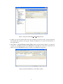
2. You can learn how the MegaWizard Plug-in Manager is used to generate a desired LPM module by reading
the tutorial Using Library Modules in Verilog Designs. This tutorial is provided in the University Program
section of Altera’s web site. In the first screen of the MegaWizard Plug-in Manager choose the RAM:
1-PORT LPM, which is found under the Memory Compiler category. As indicated in Figure 2, select
Verilog HDL as the type of output file to create, and give the file the name ramlpm.v. On the next page of
the Wizard specify a memory size of 32 eight-bit words, and select M4K as the type of RAM block. Accept
the default settings to use a single clock for the RAM’s registers, and then advance to the page shown in
Figure 3. On this page deselect the setting called ’q’ output port under the category Which ports should
be registered?. This setting creates a RAM module that matches the structure in Figure 1b, with registered
input ports and unregistered output ports. Accept defaults for the rest of the settings in the Wizard, and then
instantiate in your top-level Verilog file the module generated in ramlpm.v. Include appropriate input and
output signals in your Verilog code for the memory ports given in Figure 1b.
Figure 2: Choosing the RAM: 1-PORT LPM.
2
Figure 3: Configuring input and output ports on the RAM: 1-PORT LPM.
3. Compile the circuit. Observe in the Compilation Report that the Quartus II Compiler uses 256 bits in one of
the M4K memory blocks to implement the RAM circuit.
4. Simulate the behavior of your circuit and ensure that you can read and write data in the memory.
Part II
Now, we want to realize the memory circuit in the FPGA on the DE2 board, and use toggle switches to load some
data into the created memory. We also want to display the contents of the RAM on the 7-segment displays.
1. Make a new Quartus II project which will be used to implement the desired circuit on the DE2 board.
2. Create another Verilog file that instantiates the ramlpm module and that includes the required input and
output pins on the DE2 board. Use toggle switches SW7−0 to input a byte of data into the RAM location
identified by a 5-bit address specified with toggle switches SW15−11 . Use SW17 as the Write signal and use
KEY0 as the Clock input. Display the value of the Write signal on LEDG0 . Show the address value on the
7-segment displays HEX7 and HEX6, show the data being input to the memory on HEX5 and HEX4, and
show the data read out of the memory on HEX1 and HEX0.
3. Test your circuit and make sure that all 32 locations can be loaded properly.
Part III
Instead of directly instantiating the LPM module, we can implement the required memory by specifying its structure in the Verilog code. In a Verilog-specified design it is possible to define the memory as a multidimensional
array. A 32 x 8 array, which has 32 words with 8 bits per word, can be declared by the statement
reg [7:0] memory array [31:0];
3
In the Cyclone II FPGA, such an array can be implemented either by using the flip-flops that each logic element
contains or, more efficiently, by using the M4K blocks. There are two ways of ensuring that the M4K blocks will
be used. One is to use an LPM module from the Library of Parameterized Modules, as we saw in Part I. The other
is to define the memory requirement by using a suitable style of Verilog code from which the Quartus II compiler
can infer that a memory block should be used. Quartus II Help shows how this may be done with examples of
Verilog code (search in the Help for “Inferred memory”).
Perform the following steps:
1. Create a new project which will be used to implement the desired circuit on the DE2 board.
2. Write a Verilog file that provides the necessary functionality, including the ability to load the RAM and read
its contents as done in Part II.
3. Assign the pins on the FPGA to connect to the switches and the 7-segment displays.
4. Compile the circuit and download it into the FPGA chip.
5. Test the functionality of your design by applying some inputs and observing the output. Describe any
differences you observe in comparison to the circuit from Part II.
Part IV
The DE2 board includes an SRAM chip, called IS61LV25616AL-10, which is a static RAM having a capacity
of 256K 16-bit words. The SRAM interface consists of an 18-bit address port, A17−0 , and a 16-bit bidirectional
data port, I/O15−0 . It also has several control inputs, CE, OE, W E, U B, and LB, which are described in Table 1.
Name
Purpose
CE
OE
WE
UB
LB
Chip enable−asserted low during all SRAM operations
Output enable−can be asserted low during only read operations, or during all operations
Write enable−asserted low during a write operation
Upper byte−asserted low to read or write the upper byte of an address
Lower byte−asserted low to read or write the lower byte of an address
Table 1. SRAM control inputs.
The operation of the IS61LV25616AL chip is described in its data sheet, which can obtained from the DE2 System
CD that is included with the DE2 board, or by performing an Internet search. The data sheet describes a number
of modes of operation of the memory and lists many timing parameters related to its use. For the purposes of
this exercise a simple operating mode is to always assert (set to 0) the control inputs CE, OE, U B, and LB, and
then to control reading and writing of the memory by using only the W E input. Simplified timing diagrams that
correspond to this mode are given in Figure 4. Part (a) shows a read cycle, which begins when a valid address
appears on A17−0 and the W E input is not asserted. The memory places valid data on the I/O15−0 port after the
address access delay, tAA . When the read cycle ends because of a change in the address value, the output data
remains valid for the output hold time, tOHA .
4
t AA
A 17 – 0
t OHA
Address in
I/O 15 – 0
Data out
(a) SRAM read cycle timing
t AW
A 17 – 0
t HA
Address in
WE
t SA
I/O 15 – 0
Data in
t SD
t HD
(b) SRAM write cycle timing
Figure 4: SRAM read and write cycles.
Figure 4b gives the timing for a write cycle. It begins when W E is set to 0, and it ends when W E is set back to
1. The address has to be valid for the address setup time, tAW , and the data to be written has to be valid for the
data setup time, tSD , before the rising edge of W E. Table 2 lists the minimum and maximum values of all timing
parameters shown in Figure 4.
Parameter
Value
Min Max
tAA
−
10 ns
tOHA
3 ns
−
tAW
8 ns
−
tSD
6 ns
−
tHA
0
−
tSA
0
−
tHD
0
−
Table 2. SRAM timing parameter values.
You are to realize the 32 x 8 memory in Figure 1a by using the SRAM chip. It is a good approach to include in
your design the registers shown in Figure 1b, by implementing these registers in the FPGA chip. Be careful to
implement properly the bidirectional data port that connects to the memory.
1. Create a new Quartus II project for your circuit. Write a Verilog file that provides the necessary functionality,
including the ability to load the memory and read its contents. Use the same switches, LEDs, and 7-segment
5
displays on the DE2 board as in Parts II and III, and use the SRAM pin names shown in Table 3 to interface
your circuit to the IS61LV25616AL chip (the SRAM pin names are also given in the DE2 User Manual).
Note that you will not use all of the address and data ports on the IS61LV25616AL chip for your 32 x 8
memory; connect the unneeded ports to 0 in your Verilog module.
SRAM port name
A17−0
I/O15−0
CE
OE
WE
UB
LB
DE2 pin name
SRAM
SRAM
SRAM
SRAM
SRAM
SRAM
SRAM
ADDR17−0
DQ15−0
CE N
OE N
WE N
UB N
LB N
Table 3. DE2 pin names for the SRAM chip.
2. Compile the circuit and download it into the FPGA chip.
3. Test the functionality of your design by reading and writing values to several different memory locations.
Part V
The SRAM block in Figure 1 has a single port that provides the address for both read and write operations. For
this part you will create a different type of memory module, in which there is one port for supplying the address
for a read operation, and a separate port that gives the address for a write operation. Perform the following steps.
1. Create a new Quartus II project for your circuit. To generate the desired memory module open the MegaWizard Plug-in Manager and select the RAM: 2-PORT LPM in the Memory Compiler category. On Page 3 of
the Wizard choose the setting With one read port and one write port in the category called How will you
be using the dual port ram?. Advance through Pages 4 to 7 and make the same choices as in Part II. On
Page 8 choose the setting I don’t care in the category Mixed Port Read-During-Write for Single Input
Clock RAM. This setting specifies that it does not matter whether the memory outputs the new data being
written, or the old data previously stored, in the case that the write and read addresses are the same.
Page 10 of the Wizard is displayed in Figure 5. It makes use of a feature that allows the memory module
to be loaded with initial data when the circuit is programmed into the FPGA chip. As shown in the figure,
choose the setting Yes, use this file for the memory content data, and specify the filename ramlpm.mif.
To learn about the format of a memory initialization file (MIF), see the Quartus II Help. You will need to
create this file and specify some data values to be stored in the memory. Finish the Wizard and then examine
the generated memory module in the file ramlpm.v.
6
Figure 5: Specifying a memory initialization file (MIF).
2. Write a Verilog file that instantiates your dual-port memory. To see the RAM contents, add to your design a
capability to display the content of each byte (in hexadecimal format) on the 7-segment displays HEX1 and
HEX0. Scroll through the memory locations by displaying each byte for about one second. As each byte
is being displayed, show its address (in hex format) on the 7-segment displays HEX3 and HEX2. Use the
50 MHz clock, CLOCK 50, on the DE2 board, and use KEY0 as a reset input. For the write address and
corresponding data use the same switches, LEDs, and 7-segment displays as in the previous parts of this
exercise. Make sure that you properly synchronize the toggle switch inputs to the 50 MHz clock signal.
3. Test your circuit and verify that the initial contents of the memory match your ramlpm.mif file. Make sure
that you can independently write data to any address by using the toggle switches.
Part VI
The dual-port memory created in Part V allows simultaneous read and write operations to occur, because it has
two address ports. In this part of the exercise you should create a similar capability, but using a single-port RAM.
Since there will be only one address port you will need to use multiplexing to select either a read or write address
at any specific time. Perform the following steps.
1. Create a new Quartus II project for your circuit, and use the MegaWizard Plug-in Manager to again create
a RAM: 1-PORT LPM. For Pages 3 to 5 of the Wizard use the same settings as in Part I. On Page 6, shown
in Figure 6, specify the ramlpm.mif file as you did in Part V, but also make the setting Allow In-System
Memory Content Editor to capture and update content independently of the system clock. This
option allows you to use a feature of the Quartus II CAD system called the In-System Memory Content
Editor to view and manipulate the contents of the created RAM module. When using this tool you can
optionally specify a four-character ‘Instance ID’ that serves as a name for the memory; in Figure 7 we gave
the RAM module the name 32x8. Complete the final steps in the Wizard.
7
Figure 6: Configuring RAM: 1-PORT for use with the In-System Memory Content Editor.
2. Write a Verilog file that instantiates your memory module. Include in your design the ability to scroll
through the memory locations as in Part V. Use the same switches, LEDs, and 7-segment displays as you
did previously.
3. Before you can use the In-System Memory Content Editor tool, one additional setting has to be made. In
the Quartus II software select Assignments > Settings to open the window in Figure 7, and then open the
item called Default Parameters under Analysis and Synthesis Settings. As shown in the figure, type
the parameter name CYCLONEII SAFE WRITE and assign the value RESTRUCTURE. This parameter
allows the Quartus II synthesis tools to modify the single-port RAM as needed to allow reading and writing
of the memory by the In-System Memory Content Editor tool. Click OK to exit from the Settings window.
8
Figure 7: Setting the CYCLONEII SAFE WRITE parameter.
4. Compile your code and download the circuit onto the DE2 board. Test the circuit’s operation and ensure
that read and write operations work properly. Describe any differences you observe from the behavior of
the circuit in Part V.
5. Select Tools > In-System Memory Content Editor, which opens the window in Figure 8. To specify the
connection to your DE2 board click on the Setup button on the right side of the screen. In the window in
Figure 9 select the USB-Blaster hardware, and then close the Hardware Setup dialog.
Figure 8: The In-System Memory Content Editor window.
9
Figure 9: The Hardware Setup window.
Instructions for using the In-System Memory Content Editor tool can be found in the Quartus II Help.
A simple operation is to right-click on the 32x8 memory module, as indicated in Figure 10, and select
Read Data from In-System Memory. This action causes the contents of the memory to be displayed
in the bottom part of the window. You can then edit any of the displayed values by typing over them. To
actually write the new value to the RAM, right click again on the 32x8 memory module and select Write
All Modified Words to In-System Memory.
Experiment by changing some memory values and observing that the data is properly displayed both on the
7-segment displays on the DE2 board and in the In-System Memory Content Editor window.
Figure 10: Using the In-System Memory Content Editor tool.
Part VII
For this part you are to modify your circuit from Part VI (and Part IV) to use the IS61LV25616AL SRAM chip
instead of an M4K block. Create a Quartus II project for the new design, compile it, download it onto the DE2
boards, and test the circuit.
10
In Part VI you used a memory initialization file to specify the initial contents of the 32 x 8 RAM block, and
you used the In-System Memory Content Editor tool to read and modify this data. This approach can be used
only for the memory resources inside the FPGA chip. To perform equivalent operations using the external SRAM
chip you can use a special capability of the DE2 board called the DE2 Control Panel. Chapter 3 of the DE2 User
Manual shows how to use this tool. The procedure involves programming the FPGA with a special circuit that
communicates with the Control Panel software application, which is illustrated in Figure 11, and using this setup
to load data into the SRAM chip. Subsequently, you can reprogram the FPGA with your own circuit, which will
then have access to the data stored in the SRAM chip (reprogramming the FPGA has no effect on the external
memory). Experiment with this capability and ensure that the results of read and write operations to the SRAM
chip can be observed both in the your circuit and in the DE2 Control Panel software.
Figure 11: The DE2 Control Panel software.
c
Copyright 2011
Altera Corporation.
11
Laboratory Exercise 9
A Simple Processor
Figure 1 shows a digital system that contains a number of 16-bit registers, a multiplexer, an adder/subtracter
unit, and a control unit (finite state machine). Data is input to this system via the 16-bit DIN input. This data can
be loaded through the 16-bit wide multiplexer into the various registers, such as R0, . . . , R7 and A. The multiplexer also allows data to be transferred from one register to another. The multiplexer’s output wires are called a
bus in the figure because this term is often used for wiring that allows data to be transferred from one location in
a system to another.
Addition or subtraction is performed by using the multiplexer to first place one 16-bit number onto the bus
wires and loading this number into register A. Once this is done, a second 16-bit number is placed onto the bus,
the adder/subtracter unit performs the required operation, and the result is loaded into register G. The data in G
can then be transferred to one of the other registers as required.
16
16
R0 in
16
R7 in
R0
16
16
A in
R7
A
Clock
DIN
AddSub
16
Addsub
16
G in
Multiplexers
G
8
16
Bus
9
R0 out R7 out
G out
DIN out
IR in
IR
9
Control unit FSM
Run
Resetn
Done
Figure 1: A digital system.
The system can perform different operations in each clock cycle, as governed by the control unit. This unit
determines when particular data is placed onto the bus wires and it controls which of the registers is to be loaded
with this data. For example, if the control unit asserts the signals R0out and Ain , then the multiplexer will place
the contents of register R0 onto the bus and this data will be loaded by the next active clock edge into register A.
A system like this is often called a processor. It executes operations specified in the form of instructions.
Table 1 lists the instructions that the processor has to support for this exercise. The left column shows the name
1
of an instruction and its operand. The meaning of the syntax RX ← [RY] is that the contents of register RY are
loaded into register RX. The mv (move) instruction allows data to be copied from one register to another. For
the mvi (move immediate) instruction the expression RX ← D indicates that the 16-bit constant D is loaded into
register RX.
Operation
Function performed
mv Rx,Ry
Rx ← [Ry]
mvi Rx,#D
Rx ← D
add Rx, Ry
Rx ← [Rx] + [Ry]
sub Rx, Ry
Rx ← [Rx] − [Ry]
Table 1. Instructions performed in the processor.
Each instruction can be encoded and stored in the IR register using the 9-bit format IIIXXXYYY, where III
represents the instruction, XXX gives the RX register, and YYY gives the RY register. Although only two bits
are needed to encode our four instructions, we are using three bits because other instructions will be added to the
processor in later parts of this exercise. Hence IR has to be connected to nine bits of the 16-bit DIN input, as
indicated in Figure 1. For the mvi instruction the YYY field has no meaning, and the immediate data #D has to be
supplied on the 16-bit DIN input after the mvi instruction word is stored into IR.
Some instructions, such as an addition or subtraction, take more than one clock cycle to complete, because
multiple transfers have to be performed across the bus. The finite state machine in the control unit “steps through”
such instructions, asserting the control signals needed in successive clock cycles until the instruction has completed. The processor starts executing the instruction on the DIN input when the Run signal is asserted and the
processor asserts the Done output when the instruction is finished. Table 2 indicates the control signals that can
be asserted in each time step to implement the instructions in Table 1. Note that the only control signal asserted in
time step 0 is IRin , so this time step is not shown in the table.
T1
T2
T3
(mv): I0
RYout , RXin ,
Done
(mvi): I1
DINout , RXin ,
Done
(add): I2
RXout , Ain
RYout , Gin
Gout , RXin ,
Done
(sub): I3
RXout , Ain
RYout , Gin ,
AddSub
Gout , RXin ,
Done
Table 2. Control signals asserted in each instruction/time step.
Part I
Design and implement the processor shown in Figure 1 using Verilog code as follows:
1. Create a new Quartus II project for this exercise.
2. Generate the required Verilog file, include it in your project, and compile the circuit. A suggested skeleton
of the Verilog code is shown in parts a and b of Figure 2, and some subcircuit modules that can be used in
this code appear in Figure 2c.
3. Use functional simulation to verify that your code is correct. An example of the output produced by a
functional simulation for a correctly-designed circuit is given in Figure 3. It shows the value (2000)16 being
2
loaded into IR from DIN at time 30 ns. This pattern (the leftmost bits of DIN are connected to IR) represents
the instruction mvi R0,#D, where the value D = 5 is loaded into R0 on the clock edge at 50 ns. The
simulation then shows the instruction mv R1,R0 at 90 ns, add R0,R1 at 110 ns, and sub R0,R0 at 190 ns.
Note that the simulation output shows DIN as a 4-digit hexadecimal number, and it shows the contents of
IR as a 3-digit octal number.
4. Create a new Quartus II project which will be used for implementation of the circuit on the Altera DE2series board. This project should consist of a top-level module that contains the appropriate input and output
ports for the Altera board. Instantiate your processor in this top-level module. Use switches SW15−0 to drive
the DIN input port of the processor and use switch SW17 to drive the Run input. Also, use push button KEY0
for Resetn and KEY1 for Clock. Connect the processor bus wires to LEDR15−0 and connect the Done signal
to LEDR17 .
5. Add to your project the necessary pin assignments for the DE2-series board. Compile the circuit and download it into the FPGA chip.
6. Test the functionality of your design by toggling the switches and observing the LEDs. Since the processor’s
clock input is controlled by a push button switch, it is easy to step through the execution of instructions and
observe the behavior of the circuit.
module proc (DIN, Resetn, Clock, Run, Done, BusWires);
input [15:0] DIN;
input Resetn, Clock, Run;
output Done;
output [15:0] BusWires;
parameter T0 = 2’b00, T1 = 2’b01, T2 = 2’b10, T3 = 2’b11;
. . . declare variables
assign I = IR[1:3];
dec3to8 decX (IR[4:6], 1’b1, Xreg);
dec3to8 decY (IR[7:9], 1’b1, Yreg);
Figure 2a. Skeleton Verilog code for the processor.
3
// Control FSM state table
always @(Tstep_Q, Run, Done)
begin
case (Tstep_Q)
T0: // data is loaded into IR in this time step
if (!Run) Tstep_D = T0;
else Tstep_D = T1;
T1: . . .
endcase
end
// Control FSM outputs
always @(Tstep_Q or I or Xreg or Yreg)
begin
. . . specify initial values
case (Tstep_Q)
T0: // store DIN in IR in time step 0
begin
IRin = 1’b1;
end
T1: //define signals in time step 1
case (I)
...
endcase
T2: //define signals in time step 2
case (I)
...
endcase
T3: //define signals in time step 3
case (I)
...
endcase
endcase
end
// Control FSM flip-flops
always @(posedge Clock, negedge Resetn)
if (!Resetn)
...
regn reg_0 (BusWires, Rin[0], Clock, R0);
. . . instantiate other registers and the adder/subtracter unit
. . . define the bus
endmodule
Figure 2b. Skeleton Verilog code for the processor.
4
module dec3to8(W, En, Y);
input [2:0] W;
input En;
output [0:7] Y;
reg [0:7] Y;
always @(W or En)
begin
if (En == 1)
case (W)
3’b000: Y = 8’b10000000;
3’b001: Y = 8’b01000000;
3’b010: Y = 8’b00100000;
3’b011: Y = 8’b00010000;
3’b100: Y = 8’b00001000;
3’b101: Y = 8’b00000100;
3’b110: Y = 8’b00000010;
3’b111: Y = 8’b00000001;
endcase
else
Y = 8’b00000000;
end
endmodule
module regn(R, Rin, Clock, Q);
parameter n = 16;
input [n-1:0] R;
input Rin, Clock;
output [n-1:0] Q;
reg [n-1:0] Q;
always @(posedge Clock)
if (Rin)
Q <= R;
endmodule
Figure 2c. Subcircuit modules for use in the processor.
5
Figure 3. Simulation of the processor.
Part II
In this part you are to design the circuit depicted in Figure 4, in which a memory module and counter are connected
to the processor from Part I. The counter is used to read the contents of successive addresses in the memory, and
this data is provided to the processor as a stream of instructions. To simplify the design and testing of this circuit
we have used separate clock signals, PClock and MClock, for the processor and memory.
Processor
Memory
Counter
n
addr
Bus
16
data
16
Bus
DIN
Done
Run
Resetn
Done
MClock
PClock
Resetn
Run
Figure 4. Connecting the processor to a memory and counter.
1. Create a new Quartus II project which will be used to test your circuit.
2. Generate a top-level Verilog file that instantiates the processor, memory, and counter. Use the Quartus II
MegaWizard Plug-In Manager tool to create the memory module from the Altera library of parameterized
modules (LPMs). The correct LPM is found under the Memory Compiler category and is called ROM:
1-PORT. Follow the instructions provided by the wizard to create a memory that has one 16-bit wide read
data port and is 32 words deep. Page 4 of the wizard is shown in Figure 5. Since this memory has only a
read port, and no write port, it is called a synchronous read-only memory (synchronous ROM). Note that the
6
memory includes a register for synchronously loading addresses. This register is required due to the design
of the memory resources on the Cyclone FPGA; account for the clocking of this address register in your
design.
To place processor instructions into the memory, you need to specify initial values that should be stored in
the memory once your circuit has been programmed into the FPGA chip. This can be done by telling the
wizard to initialize the memory using the contents of a memory initialization file (MIF). The appropriate
screen of the MegaWizard Plug-In Manager tool is illustrated in Figure 6. We have specified a file named
inst_mem.mif, which then has to be created in the directory that contains the Quartus II project. Use the
Quartus II on-line Help to learn about the format of the MIF file and create a file that has enough processor
instructions to test your circuit.
3. Use functional simulation to test the circuit. Ensure that data is read properly out of the ROM and executed
by the processor.
4. Make sure your project includes the necessary port names and pin location assignments to implement the
circuit on the DE2-series board. Use switch SW17 to drive the processor’s Run input, use KEY0 for Resetn,
use KEY1 for MClock, and use KEY2 for PClock. Connect the processor bus wires to LEDR15−0 and connect
the Done signal to LEDR17 .
5. Compile the circuit and download it into the FPGA chip.
6. Test the functionality of your design by toggling the switches and observing the LEDs. Since the circuit’s
clock inputs are controlled by push button switches, it is easy to step through the execution of instructions
and observe the behavior of the circuit.
Figure 5. 1-PORT configuration.
7
Figure 6. Specifying a memory initialization file (MIF).
Enhanced Processor
It is possible to enhance the capability of the processor so that the counter in Figure 4 is no longer needed, and
so that the processor has the ability to perform read and write operations using memory or other devices. These
enhancements involve adding new instructions to the processor and the programs that the processor executes are
therefore more complex; they are described in a subsequent lab exercise available from Altera.
c
Copyright 2011
Altera Corporation.
8
Laboratory Exercise 10
An Enhanced Processor
In Laboratory Exercise 9 we described a simple processor. In Part I of that exercise the processor itself was
designed, and in Part II the processor was connected to an external counter and a memory unit. This exercise
describes subsequent parts of the processor design. Note that the numbering of figures and tables in this exercise
are continued from those in Parts I and II in the preceding lab exercise.
Part III
In this part you will extend the capability of the processor so that the external counter is no longer needed, and
so that the processor has the ability to perform read and write operations using memory or other devices. You
will add three new types of instructions to the processor, as displayed in Table 3. The ld (load) instruction loads
data into register RX from the external memory address specified in register RY. The st (store) instruction stores
the data contained in register RX into the memory address found in RY. Finally, the instruction mvnz (move if
not zero) allows a mv operation to be executed only under a certain condition; the condition is that the current
contents of register G are not equal to 0.
Operation
Function performed
ld Rx,[Ry]
Rx ← [[Ry]]
st Rx,[Ry]
[Ry] ← [Rx]
mvnz Rx, Ry
if G != 0, Rx ← [Ry]
Table 3. New instructions performed in the processor.
A schematic of the enhanced processor is given in Figure 7. In this figure, registers R0 to R6 are the same
as in Figure 1 of Laboratory Exercise 9, but register R7 has been changed to a counter. This counter is used
to provide the addresses in the memory from which the processor’s instructions are read; in the preceding lab
exercise, a counter external to the processor was used for this purpose. We will refer to R7 as the processor’s
program counter (PC), because this terminology is common for real processors available in the industry. When
the processor is reset, PC is set to address 0. At the start of each instruction (in time step 0) the contents of PC
are used as an address to read an instruction from the memory. The instruction is stored in IR and the PC is
automatically incremented to point to the next instruction (in the case of mvi the PC provides the address of the
immediate data and is then incremented again).
The processor’s control unit increments PC by using the incr_PC signal, which is just an enable on this counter.
It is also possible to directly load an address into PC (R7) by having the processor execute a mv or mvi instruction
in which the destination register is specified as R7. In this case the control unit uses the signal R7in to perform
a parallel load of the counter. In this way, the processor can execute instructions at any address in memory, as
opposed to only being able to execute instructions that are stored in successive addresses. Similarly, the current
contents of PC can be copied into another register by using a mv instruction. An example of code that uses the
PC register to implement a loop is shown below, where the text after the % on each line is just a comment. The
instruction mv R5,R7 places into R5 the address in memory of the instruction sub R4,R2. Then, the instruction
mvnz R7,R5 causes the sub instruction to be executed repeatedly until R4 becomes 0. This type of loop could be
used in a larger program as a way of creating a delay.
mvi
mvi
mv
sub
mvnz
R2,#1
R4,#10000000
R5,R7
R4,R2
R7,R5
% binary delay value
% save address of next instruction
% decrement delay count
% continue subtracting until delay count gets to 0
1
Bus
16
16
incr_pc
R7 in
R0
E
L
16
16
A in
Counter
(R7)
A
Clock
DIN
AddSub
16
Addsub
ADDR
R0 in
ADDR
DOUT
16
DOUT
16
G in
Multiplexers
G
8
16
9
DIN out
R0 out R7 out
G out
IR in
ADDR in
IR
DOUT in
9
Control FSM
W_D
W
Run
Resetn
Done
Figure 7. An enhanced version of the processor.
Figure 7 shows two registers in the processor that are used for data transfers. The ADDR register is used to
send addresses to an external device, such as a memory module, and the DOUT register is used by the processor to
provide data that can be stored outside the processor. One use of the ADDR register is for reading, or fetching, instructions from memory; when the processor wants to fetch an instruction, the contents of PC (R7) are transferred
across the bus and loaded into ADDR. This address is provided to memory. In addition to fetching instructions,
the processor can read data at any address by using the ADDR register. Both data and instructions are read into the
processor on the DIN input port. The processor can write data for storage at an external address by placing this
address into the ADDR register, placing the data to be stored into its DOUT register, and asserting the output of
the W (write) flip-flop to 1.
Figure 8 illustrates how the enhanced processor is connected to memory and other devices. The memory unit in
the figure supports both read and write operations and therefore has both address and data inputs, as well as a write
enable input. The memory also has a clock input, because the address, data, and write enable inputs must be loaded
into the memory on an active clock edge. This type of memory unit is usually called a synchronous random access
memory (synchronous RAM). Figure 8 also includes a 16-bit register that can be used to store data from the processor; this register might be connected to a set of LEDs to allow display of data on the DE2-series board. To allow
the processor to select either the memory unit or register when performing a write operation, the circuit includes
some logic gates that perform address decoding: if the upper address lines are A15 A14 A13 A12 = 0000, then the
memory module will be written at the address given on the lower address lines. Figure 8 shows n lower address
lines connected to the memory; for this exercise a memory with 128 words is probably sufficient, which implies
that n = 7 and the memory address port is driven by A6 . . . A0 . For addresses in which A15 A14 A13 A12 = 0001,
2
the data written by the processor is loaded into the register whose outputs are called LEDs in Figure 8.
A 12
…
A 15
Processor
ADDR
DOUT
Memory
4
16
n
16
addr
data
DIN
q
16
wr_en
W
Done
A 12
…
Resetn
Run
4
A 15
Clock
E
Resetn
16
Run
D
Q
LEDs
Figure 8. Connecting the enhanced processor to a memory and output register.
1. Create a new Quartus II project for the enhanced version of the processor.
2. Write Verilog code for the processor and test your circuit by using functional simulation: apply instructions
to the DIN port and observe the internal processor signals as the instructions are executed. Pay careful
attention to the timing of signals between your processor and external memory; account for the fact that the
memory has registered input ports, as we discussed for Figure 8.
3. Create another Quartus II project that instantiates the processor, memory module, and register shown in Figure 8. Use the Quartus II MegaWizard Plug-In Manager tool to create the RAM: 1-PORT memory module.
Follow the instructions provided by the wizard to create a memory that has one 16-bit wide read/write data
port and is 128 words deep. Use a MIF file to store instructions in the memory that are to be executed by
your processor.
4. Use functional simulation to test the circuit. Ensure that data is read properly from the RAM and executed
by the processor.
5. Include in your project the necessary pin assignments to implement your circuit on the DE2-series board.
Use switch SW17 to drive the processor’s Run input, use KEY0 for Resetn, and use the board’s 50 MHz
clock signal as the Clock input. Since the circuit needs to run properly at 50 MHz, make sure that a timing
constraint is set in Quartus II to constrain the circuit’s clock to this frequency. Read the Report produced by
the Quartus II Timing Analyzer to ensure that your circuit operates at this speed; if not, use the Quartus II
tools to analyze your circuit and modify your Verilog code to make a more efficient design that meets the
50-MHz speed requirement. Also note that the Run input is asynchronous to the clock signal, so make sure
to synchronize this input using flip-flops.
Connect the LEDs register in Figure 8 to LEDR15−0 so that you can observe the output produced by the
processor.
6. Compile the circuit and download it into the FPGA chip.
7. Test the functionality of your design by executing code from the RAM and observing the LEDs.
3
Part IV
In this part you are to connect an additional I/O module to your circuit from Part III and write code that is executed
by your processor.
Add a module called seg7_scroll to your circuit. This module should contain one register for each 7-segment
display on the DE2-series board. Each register should directly drive the segment lights for one 7-segment display,
so that the processor can write characters onto these displays. Create the necessary address decoding to allow the
processor to write to the registers in the seg7_scroll module.
1. Create a Quartus II project for your circuit and write the Verilog code that includes the circuit from Figure 8
in addition to your seg7_scroll module.
2. Use functional simulation to test the circuit.
3. Add appropriate timing constraints and pin assignments to your project, and write a MIF file that allows
the processor to write characters to the 7-segment displays. A simple program would write a word to the
displays and then terminate, but a more interesting program could scroll a message across the displays, or
scroll a word across the displays in the left, right, or both directions.
4. Test the functionality of your design by executing code from the RAM and observing the 7-segment displays.
Part V
Add to your circuit from Part IV another module, called port_n, that allows the processor to read the state of
some switches on the board. The switch values should be stored into a register, and the processor should be able
to read this register by using a ld instruction. You will have to use address decoding and multiplexers to allow the
processor to read from either the RAM or port_n units, according to the address used.
1. Draw a circuit diagram that shows how the port_n unit is incorporated into the system.
2. Create a Quartus II project for your circuit, write the Verilog code, and write a MIF file that demonstrates
use of the port_n module. One interesting application is to have the processor scroll a message across the 7segment displays and use the values read from the port_n module to change the speed at which the message
is scrolled.
3. Test your circuit both by using functional simulation and by downloading it and executing your processor
code on the DE2-series board.
Suggested Bonus Parts
The following are suggested bonus parts for this exercise.
1. Use the Quartus II tools to identify the critical paths in the processor circuit. Modify the processor design
so that the circuit will operate at the highest clock frequency that you can achieve.
2. Extend the instructions supported by your processor to make it more flexible. Some suggested instruction
types are logic instructions (AND, OR, etc), shift instructions, and branch instructions. You may also wish
to add support for logical conditions other than “not zero” , as supported by mvnz, and the like.
3. Write an Assembler program for your processor. It should automatically produces a MIF file from assembly
language code.
c
Copyright 2011
Altera Corporation.
4
Laboratory Exercise 11
Implementing Algorithms in Hardware
This is an exercise in using algorithmic state machine charts to implement algorithms as hardware circuits.
Background
Algorithmic State Machine (ASM) charts are an alternative representation for finite state machines, which allow designers to express larger state machines and circuits in a manner similar to a flow chart. An example of an
ASM chart is shown in Figure 1. It represents a circuit that counts the number of bits set to 1 in an n-bit input A
(A = an−1 an−2 ..a1 a0 ).
Reset
S1
Load A
result = 0
0
0
s
s
1
S2
1
S3
right-shift A
Done
1
A==0
result++
0
0
a0
1
Figure 1: ASM chart for a bit counting circuit.
In this ASM chart, state S1 is the initial state where we load input into shirt register A and wait for the start (s)
signal to begin operation. We then counter the number of 1’s in A in state S2, and wait in state S3 when counting
is completed.
The key distinction between ASM and flow charts is in what is known as implied timing. In contrast to a flow
1
chart, events that stem from a single state (rectangle) box in an ASM chart are considered to happen in the same
clock cycle. Any synchronous elements, such as counters or registers, update their value when the next state is
reached. Thus, the correct way to interpret the highlighted state in Figure 1 is as follows.
In state S2, the shift register A is enabled to shift contents at the next positive edge of the clock. Simultaneously,
its present value is tested to check if it is equal to 0. If A is not 0, then we check if the least-significant bit of A
(a0 ) is 1. If it is, then the counter named result will be incremented at the next positive edge of the clock. If A is
0, then we proceed to state S3.
The implementation of the bit counting circuit consists of components controlled by an FSM that functions
according to the ASM chart - we refer to these components as the datapath. The datapath components include a
counter to store result and a shift register A.
In this exercise you will design and implement several circuits using ASM charts.
Part I
Implement the bit-counting circuit using the ASM chart shown in Figure 1 on a DE2-series board. The inputs
to your circuit should consist of an 8-bit input connected to slider switches SW7−0 , an asynchronous reset connected to KEY0 , and a start signal (s) connected to switch SW8 . Your circuit should display the number of 1s in
the given 8-bit input value using red LEDs, and signal that the algorithm is finished by lighting up a green LED.
Part II
We wish to implement a binary search algorithm, which searches through an array to locate an 8-bit value A
specified via switches SW7−0 . A block diagram for the circuit is shown in Figure 2.
A7-0
Data_out
Start
Reset
Your FSM
Memory
Address
Your Datapath
L4-0
Found
Figure 2: A block diagram for a circuit that performs a binary search.
The binary search algorithm works on a sorted array. Rather than comparing each value in the array to the
one being sought, we first look at the middle element and compare the sought value to the middle element. If the
middle element has a greater value, then we know that the element we seek must be in the first half of the array.
Otherwise, the value we seek must be in the other half of the array. By applying this approach recursively, we can
locate the sought element in only a few steps.
In this circuit, the array is stored in an on-chip memory instantiated using MegaWizard Plug-In Manager. To
create the approriate memory block, use the the RAM: 1-PORT module from the MegaWizard Plug-In Manager
as shown in Figure 3.
2
Figure 3: Single-port memory selection using MegaWizard Plug-In Manager.
In the window in Figure 3, specify the Verilog HDL output file to be memory_block.v. When creating the
memory block, you should also specify a memory initilization file to be my_array.mif, so that the memory contents
can be set to contain an ordered array of numbers.
The circuit should produce a 5-bit value L that specifies the address in the memory where the number A is
located. In addition, a signal Found should be set high to indicate that the number A was found in the memory,
and set low otherwise.
Perform the following steps:
1. Create an ASM chart for the binary search algorithm. Keep in mind that it takes two clock cycles for the
data to be read from memory. You may assume that the array has a fixed size of 32 elements.
2. Implement the FSM and the datapath for your circuit.
3. Connect your FSM and datapath to the memory block as shown in Figure 2.
4. Include in your project the necessary pin assignments to implement your circuit on the DE2-series board.
Use switch SW8 to drive the processor’s Run input, use SW7 to SW0 to specify the value to be searched, use
KEY0 for Resetn, and use the board’s 50 MHz clock signal as the Clock input. Connect LEDR4 to LEDR0
to show the address in memory of the number A, and LEDG0 for the Found signal.
5. Create a file called my_array.mif and fill it with an ordered set of 32 eight-bit integer numbers. You can
do this in Quartus II by choosing File > New... from the main menu and selecting Memory Initialization
File. This will open a memory file editor, where the contents of the memory may be specified. After this file
is created and/or modified, your design needs to be fully recompiled, and downloaded onto the DE2-series
board for the changes to take effect.
Preparation
The recommended preparation for this exercise is to write Verilog code for Parts I and II.
c
Copyright 2011
Altera Corporation.
3
Laboratory Exercise 12
Basic Digital Signal Processing
This exercise is suggested for students who want to use the Audio CODEC on a Altera DE2-series board for
their project in an introductory digital logic course. Students will design circuit that takes input from an Audio
CODEC, alters the sound from the microphone by filtering out noise, and produces the resulting sound through
the speakers. In addition to a DE2-series board, a microphone and speakers will be required.
Background
Sounds, such as speech and music, are signals that change over time. The amplitude of a signal determines the
volume at which we hear it. The way the signal changes over time determines the type of sounds we hear. For
example, an ’ah’ sound is represented by a waveform shown in Figure 1.
Figure 1: A waveform for an ’ah’ sound.
The waveform is an analog signal, which can be stored in a digital form by using a relatively small number of
samples that represent the analog values at certain points in time. The process of producing such digital signals is
called sampling.
Figure 2: A sampled waveform for an ’ah’ sound.
1
The points in Figure 2 provide a sampled waveform. All points are spaced equally in time and they trace the
original waveform.
The Altera DE2-series board is equipped with an audio CODEC capable of sampling sound from a microphone
and providing it as input to a circuit. By default, the CODEC provides 48000 samples per second, which is
sufficient to accurately represent audible sounds.
In this exercise you will create several designs that take input from an Audio CODEC on the Altera DE2-series
board, record and process the sound from a microphone, and play it back through the speakers. To simplify your
task, a simple system that can record and playback sounds on an Altera DE2-series board is provided for you. The
system, shown in Figure 3, comprises a Clock Generator, an Audio CODEC Interface, and an Audio/Video
Configuration modules. This interface is a simplified version of the Altera University Program Audio IP Cores
you can find at http://university.altera.com.
I2C_SCLK
I2C_SDAT
Audio/Video
Configuration
CLOCK_50
read_ready
write_ready
read
write
readdata_left
readdata_right
writedata_left
writedata_right
AUD_BCLK
AUD_ADCLRCK
AUD_DACLRCK
AUD_ADCDAT
Audio
CODEC
Interface
AUD_DACDAT
Your Circuit
AUD_XCK
CLOCK_27
Clock Generator
Figure 3: Audio System for this exercise.
The left-hand side of Figure 3 shows the inputs and outputs of the system. These I/O ports supply the clock
inputs, as well as connect the Audio CODEC and Audio/Video Configuration modules to the corresponding
peripheral devices on the Altera DE2-series board. In the middle, a set of signals to and from the Audio CODEC
Interface module is shown. These signals allow your circuit, depicted on the right-hand side, to record sounds
from a microphone and play them back via speakers.
The system works as follows. Upon reset, the Audio/Video Configuration begins an autoinitialization sequence. The sequence sets up the audio device on the Altera DE2-series board to sample microphone input at a
rate of 48kHz and produce output through the speakers at the same rate. Once the autoinitialization is complete,
the Audio CODEC begins reading the data from the microphone once every 48000th of a second, and sends it
to the Audio CODEC Interface core in the system. Once received, the sample is stored in a 128-element buffer
in the Audio CODEC Interface core. The first element of the buffer is always visible on the readdata left and
readdata right outputs when the read ready signal is asserted. The next element can be read by asserting the
read signal, which ejects the current sample and a new one appears one or more clock cycles later, if read ready
signal is asserted.
To output sound through the speakers a similar procedure is followed. Your circuit should observe the
write ready signal, and if asserted write a sample to the Audio CODEC by providing it at the writedata left
and writedata right inputs and asserting the write signal. This operation stores a sample in a buffer inside of the
Audio CODEC Interface, which will then send the sample to the speakers at the right time.
A starter kit that contains this design is provided in a starterkit as part of this exercise.
2
Part I
In this part of the exercise, you are to make a simple modification to the provided circuit to pass the input from
the microphone to the speakers. You should take care to read data from and write data to the Audio CODEC
Interface only when its ready signals are asserted.
Compile your circuit and download it onto the Altera DE2-series board. Connect microphone and speakers to
the Mic and Line Out ports of the DE2-series board and speak to the microphone to hear your voice through the
speakers. After resetting the circuit, you should hear your own voice through the speakers when you talk to the
microphone.
Part II
In this part, you will learn a basic signal processing technique known as filtering. Filtering is a process of adjusting
a signal - for example, removing noise. Noise in a sound waveform is represented by small, but frequent changes
to the amplitude of the signal. A simple logic circuit that achieves the task of noise-filtering is an averaging Finite
Impulse Response (FIR) filter. The schematic diagram of the filter is shown in Figure 4.
Data in
DQ
24
÷8
DQ
DQ
DQ
DQ
DQ
DQ
÷8
÷8
÷8
÷8
÷8
÷8
÷8
+
+
+
+
+
+
+
24
Data out
Figure 4: A simple averaging FIR filter.
An averaging filter, like the one shown in Figure 4, removes noise from a sound by averaging the values of
adjacent samples. In this particular case, it removes small deviations in sound by looking at changes in the adjacent
8 samples. When using low-quality microphones, this filter should remove the noise produced when you speak to
the microphone, making your voice sound clearer.
You are to implement the circuit shown in Figure 4 to process the sound from the microphone, and output
the filtered sound through the speakers. Do you notice any difference between the quality of sound in this part as
compared to Part I?
NOTE:
It is possible to obtain high-quality microphone with noise-cancelling capabilities. In such circumstances, you are
unlikely to hear any effect from using this filter. If this is the case, we suggest introducing some noise into the
sound by adding the output of the circuit in Figure 5 to the sample produced by the Audio CODEC.
The circuit is a simple counter, whose value should be interpreted as a signed value. The circuit should be
clocked by a 50MHz clock, and the enable signal should be driven high when the Audio CODEC module can
both produce and accept a new sample.
To hear the effect of the noise generator, add the values produced by the circuit to each sample of sound from
the Audio CODEC in the circuit in part I.
Part III
The implementation of the averaging filter in part II may have been effective in removing some of the noise, and
3
module noise generator (clk, enable, Q);
input clk, enable;
output [23:0] Q;
reg [2:0] counter;
always@(posedge clk)
if (enable)
counter = counter + 1’b1;
assign Q = {{10{counter[2]}}, counter, 11’d0};
endmodule
Figure 5: Circuit to generate some noise.
all of the noise produced by the noise generator. However, if your microphone is of low-quality or you increate
the width of the counter in the noise generator, the filter in part II would be insufficient to remove the noise. The
reason for this is because the filter in part II only looked at a very small time frame over which the sound waveform
was changing. This can be remedied by making the filter larger, taking an average of more samples.
In this part, you are to experiment with the size of the filter to determine the number of samples over which
you have to average sound input to remove background noise. To do this more effectively, use the design of an
averaging FIR filter shown in Figure 6.
Data in
24
÷N
Datain
Dataout
FIFO of size N
Accumulator
QD
*(-1)
+
+
24
Data out
Figure 6: N-sample averaging FIR filter.
To compute the average of the last N samples, this circuit first divides the input sample by N . Then, the
resulting value is stored it in a First-In First-out (FIFO) buffer of length N and added to the accumulator. To make
sure the value in the accumulator is the average of the last N samples, the circuit subtracts the value that comes
out of the FIFO, which represents the (n + 1)th sample.
Implement, compule and download the circuit onto Altera DE2-series board. Connect microphone and speakers to the Mic and Line Out ports of the DE2-series board and speak to the microphone to hear your voice through
the speakers. Experiment with different values of N to see what happens to your voice and any background noise,
remembering to divide the samples by appropriate value. We recommend experimenting with values of N that are
a power of 2, to make the division easier.
If you have a portable music player, with a connector such that you can supply input to your circuit through
the Mic port, try experimenting with different sizes of the filter and its effect on the song you play.
c
Copyright 2011
Altera Corporation.
4