1
20-S3-CC410-042001
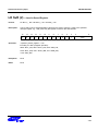
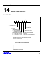
USER'S MANUAL
S3CC410
16-Bit CMOS
Microcontroller
Revision 0
S3CC410 (Preliminary Spec)
1
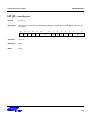
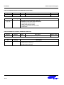
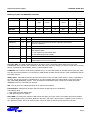
PRODUCT OVERVIEW
PRODUCT OVERVIEW
INTRODUCTION
S3CC410 single-chip CMOS microcontroller is designed for high-quality audio platform. It uses Samsung's newest
16-bit microcontroller, CalmRISC16 and 24-bit DSP engine, CalmMAC24.
FEATURES
CalmRISC16
•
16-bit low power & high performance RISC
microcontroller
•
Harvard style architecture : 4M byte program
memory space, 4M byte data memory space
•
5-stage pipelined instruction execution
•
16-bit instruction set
•
Sixteen 16-bit general purpose registers with eight
6-bit extension registers
access to control it
Internal Memory
•
Data memory : 48K byte SRAM for X memory,
24K byte SRAM for Y memory
•
Program memory : 16K byte SRAM for instruction
Cache Memory
•
Instruction cache : 4K byte direct-mapped cache
•
Data cache : 4K byte 2-way set associative
cache
CalmMAC24
•
24-bit high performance fixed-point DSP
coprocessor for CalmRISC16 microcontroller
Basic Timer & Watchdog Timer
•
1 cycle 24×24 MAC operation
•
•
Programmable basic timer (8-bit counter) &
watchdog timer (3-bit counter)
32K word (1 word = 24-bit) X data memory space
& 32K word Y data memory space
•
8 kinds of clock source
•
2 multiplier accumulator registers, 4 general
accumulator registers, and 8 pointer registers
•
Overflow of 8-bit counter makes a basic timer
interrupt and controls the oscillation warm-up time
•
Overflow of 3-bit counter makes a system reset
CalmBreaker16
Provides integrated on-chip debug support for
CalmRISC16
16-bit Timer
•
Programmable interval timer
Supports program/data address/value, watchpoint,
or realtime-view and their combinations with Four
event channels
•
Three 16-bit timers
•
Supports program downloads and uploads
•
Real time clock generation (0.5 or 1 second)
•
Supports parallel JTAG access or serial UART
•
Buzzer signal generation (1, 2, 4, or 8 kHz)
•
•
Real Time Clock
1-1
PRODUCT OVERVIEW
S3CC410 (Preliminary Spec)
FEATURES (Continued)
Serial I/O interface
SSFDC (SmartMedia) Interface
•
8-bit transmit/receive or 8-bit receive mode
•
LSB first or MSR first transmission selectable
•
Internal & external clock source
LCD Controller
Random Number Generator
•
Random number generation using LFSR (Linear
Feedback Shift Register)
External Interrupt
•
Support multiple screen size and multiple pixel
rates
•
•
Supports color/gray/monochrome STN LCD
(passive display mode)
A/D Converter
•
Supports color TFT LCD (active display mode)
I2C/I2S Interface
•
10 sources
Eight 10-bit resolution channels and
normal input
Power Down Mode
•
1 channel multi-master I C controller
•
Idle mode : only CPU clock stop
•
2 channel Sony/Philips I2S controller
•
Stop mode : system clock and CPU clock stop
2
UART Interface
Oscillation Sources
•
•
Clock synthesizer (Phase-locked loop circuit)
based on 32.768 kHz
•
CPU clock divider circuit (divided by 1, 2, 4, 8, 16,
32, 64, and 128)
Full-duplex UART controller
USB Specification Compliance (Ver 1.0, Ver 1.1)
•
Built-in full speed transceiver
•
Support 1 device address and 4 endpoints
•
One control endpoint and 3 data endpoints
•
One 16 bytes endpoint, one 32 bytes endpoint,
and two 64 bytes endpoints
•
Each data endpoint can be configurable as
interrupt, bulk and isochronous
Operating Condition
•
Temperature : -40 °C – 85 °C
•
Voltage : 3.0V – 3.6V
•
Frequency : 80 MHz
Package Type
Parallel Port Interface
•
Interrupt-based operation
•
Support IEEE standard 1284 communication
mode (compatibility, nibble, byte, and ECP mode)
•
Support ECP protocol with or without run-length
encoding
•
Automatic handshaking mode for any forward or
reverse protocol with software enable/disable
1-2
•
208-QFP
S3CC410 (Preliminary Spec)
PRODUCT OVERVIEW
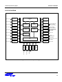
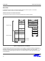
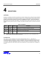
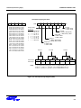
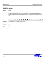
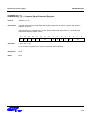
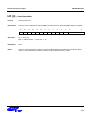
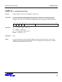
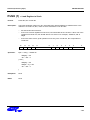
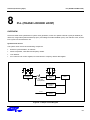
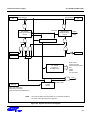
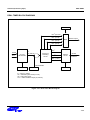
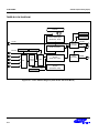
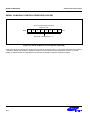
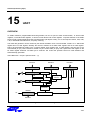
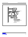
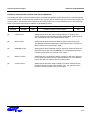
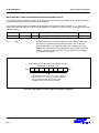
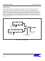
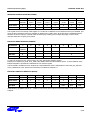
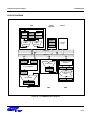
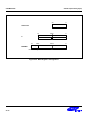
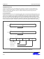
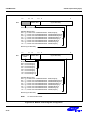
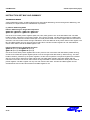
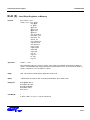
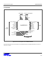
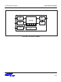
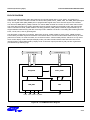
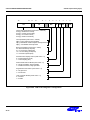
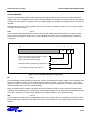
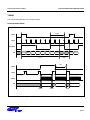
BLOCK DIAGRAM
Port 10
Port 6
P5.0-P5.7
Port 5
P4.0-P4.2
Port 4
P3.0-P3.7
Port 3
P2.0-P2.7
Port 2
Y-MEM
24-Kbyte SRAM
Instruction
Memory
16-Kbyte SRAM
SIO/UART
IIC/IIS
SI, Rx, SDA, SOI
SO, Tx, SOD
SCK, SCL, SOC
Timer A/B/C
TACK/TBCK
TAOUT/TBOUT
PPIC
BUSY/PERROR
nSTROBE, nINIT
PD0-PD7
USB
DP, DM
ADC
AVref
ADC0-ADC5
LCD
Controller
CalmMAC24
DSP
SSFDC
VD0-VD15
PCLK, LCLK, FCLK
ACBIAS
I/O0-I/O7
CalmBreaker16
Debugger
P6.0-P6.7
Instruction
Cache
4-Kbyte SRAM
DMA Controller
(YDMA, DDMA)
Port 7
X-MEM
48-Kbyte SRAM
OSC & PLL
(w/ RTC)
P7.0-P7.7
Data Cache
4-Kbyte SRAM
XO, BUZ
XI
Port 8
Port 0
P8.0-P8.3
Random
Number Gen.
P0.0-P0.7
Port 9
Port 1
P9.0-P9.6
Basic Timer
(w/ WDT)
CalmRISC
CPU
P1.0-P1.4
P10.0-P10.7
Figure 1-1. S3CC410 Top Block Diagram
1-3
PRODUCT OVERVIEW
S3CC410 (Preliminary Spec)
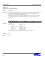
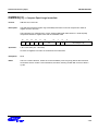
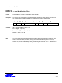
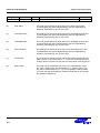
156
155
154
153
152
151
150
149
148
147
146
145
144
143
142
141
140
139
138
137
136
135
134
133
132
131
130
129
128
127
126
125
124
123
122
121
120
119
118
117
116
115
114
113
112
111
110
109
108
107
106
105
NSCS2
NSCS1
NSCS0
NRAS
NDWE
NDCS
VDD
NCAS
BA.1
BA.0
TMODE
NEXPACK
nRESETO
nRESET
PCLK
VSS
LCLK
FCLK
AC_BIAS
VD_LCD.7
VD_LCD.6
VDD
VD_LCD.5
VD_LCD.4
VD_LCD.3
VD_LCD.2
VD_LCD.1
VD_LCD.0
P10.7
VSS
P10.6
P10.5
P10.4
P10.3
P10.2
VDD
P10.1
P10.0
EVMAT.3
EVMAT.2
EVMAT.1
EVMAT.0
EXTBK.3
EXTBK.2
EXTBK.1
EXTBK.0
VSS
TDOTXD
RUNST
EVBP
UCLK
TMS
I/O DESCRIPTION
VSS
NSCS3
NSOE
NSWE
CKE
DQM
VDD
ICLK
EXTDA.0
EXTDA.1
EXTDA.2
EXTDA.3
EXTDA.4
VSS
EXTDA.5
EXTDA.6
EXTDA.7
EXTDA.8
EXTDA.9
VDD
EXTDA.10
EXTDA.11
EXTDA.12
EXTDA.13
EXTDA.14
VSS
EXTDA.15
EXTDA.16
EXTDA.17
EXTDA.18
EXTDA.19
VDD
EXTDA.20
DB.0
DB.1
DB.2
DB.3
DB.4
VSS
DB.5
DB.6
DB.7
DB.8
DB.9
VDD
DB.10
DB.11
DB.12
DB.13
DB.14
DB.15
VSS
157
158
159
160
161
162
163
164
165
166
167
168
169
170
171
172
173
174
175
176
177
178
179
180
181
182
183
184
185
186
187
188
189
190
191
192
193
194
195
196
197
198
199
200
201
202
203
204
205
206
207
208
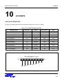
S3CC410
208-QFP
104
103
102
101
100
99
98
97
96
95
94
93
92
91
90
89
88
87
86
85
84
83
82
81
80
79
78
77
76
75
74
73
72
71
70
69
68
67
66
65
64
63
62
61
60
59
58
57
56
55
54
53
52
51
50
49
48
47
46
45
44
43
42
41
40
39
38
37
36
35
34
33
32
31
30
29
28
27
26
25
24
23
22
21
20
19
18
17
16
15
14
13
12
11
10
9
8
7
6
5
4
3
2
1
P3.6
P3.5
P3.4
P3.3
P3.2
P3.1
P3.0
VSS_PLL1
CZ1
CP1
VDD_PLL1
VSS_PLL0
CZ0
CP0
VDD_PLL0
VSS_USB
VDD_USB
AVREF
VSS_ADC
VDD_ADC
P2.7
P2.6
P2.5
P2.4
VSS
P2.3
P2.2
P2.1
P2.0
P1.4
VDD
P1.3
P1.2
P1.1
P1.0
XTI
XO
XI
VSS
XISEL
XIA
DP
DM
P0.7
P0.6
VDD
P0.5
P0.4
P0.3
P0.2
P0.1
P0.0
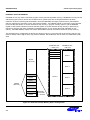
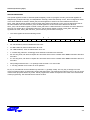
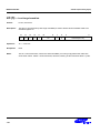
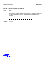
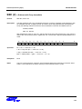
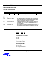
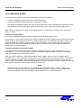
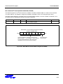
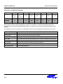
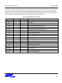
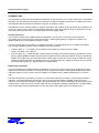
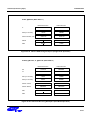
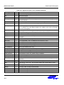
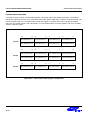
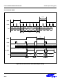
Figure 1-2. S3CC410 Pin Diagram
1-4
JTAGSEL
TDIRXD
TCKMCLK
NTRST
NGIDISX
BKREQX
VDD
P9.6
P9.5
P9.4
P9.3
P9.2
P9.1
P9.0
VSS
P8.3
P8.2
P8.1
P8.0
P7.7
P7.6
VDD
P7.5
P7.4
P7.3
P7.2
P7.1
P7.0
VSS
P6.7
P6.6
P6.5
P6.4
P6.3
P6.2
P6.1
VDD
P6.0
P5.7
P5.6
P5.5
P5.4
P5.3
P5.2
VSS
P5.1
P5.0
P4.2
P4.1
P4.0
P3.7
VDD
S3CC410 (Preliminary Spec)
PRODUCT OVERVIEW
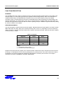
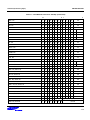
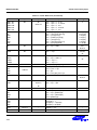
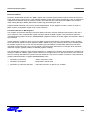
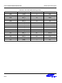
Table 1-1. S3CC410 Pin Description
Name
Type
P0.0-P0.7
I/O
Description
I/O port with bit programmable pins; Input or output
mode selected by software; Alternatively used as
parallel port data bus PD0-PD7.
Circuit
Type
Number
Shared
Pins
1
1-6,8-9
PD0-PD7
1
18-21,23
NACK
BUSY
SELECT
PERROR
NFAULT
4
24-27,
29-32
TACK
TAOUT
TBCK
TBOUT
BUZ
RX
TX
FVCO
5
46-52,
54
SI
SO
SCK
SCL
SDA
6, 3
55-57
INT8-INT9
CE2
P0.0/PD0-P0.7/PD7: Parallel port data bus
P1.0-P1.4
I/O
I/O port with bit programmable pins; Input or output
mode selected by software; Alternatively used as
parallel port control pins, NACK, BUSY, SELECT,
PERROR, and NFAULT pin.
P1.0/NACK: Not parallel port acknowledge
P1.1/BUSY: Parallel port busy
P1.2/SELECT: Parallel port select
P1.3/PERROR: Parallel port paper error
P1.4/NFAULT: Not parallel port fault
P2.0-P2.7
I/O
I/O port with bit programmable pins; Input or output
mode selected by software; Alternatively used as
TACK, TAOUT, TBCK, TBOUT, BUZ, RX, TX, and
FVCO pin.
P2.0/TACK: Timer A clock input
P2.1/TAOUT: Timer A capture input or PWM output
P2.2/TBCK: Timer B clock input
P2.3/TBOUT: Timer B capture input or PWM output
P2.4/BUZ: Buzzer output
P2.5/RX: Receive input for UART
P2.6/TX: Transmit output for UART
P2.7/FVCO: FVCO output
P3.0-P3.7
I/O
I/O port with bit programmable pins; Input or output
mode selected by software; Alternatively used as SI,
SO, SCK, SCL, SDA pin. N-channel open drains are
configurable.
P3.0/SI: Serial data input for SIO
P3.1/SO: Serial data output for SIO
P3.2/SCK: Serial clock for SIO
P3.3/SCL: Serial clock for I2C
P3.4/SDA: Serial data for I2C
P3.5-P3.7: Normal in/out
P4.0-P4.2
I/O
I/O port with bit programmable pins; Input or output
mode selected by software; Alternatively used as
inputs for external interrupts INT8-INT9 and assigned
pull-up by software, and output for CE2.
P4.0/INT8: Ext Interrupt 8
P4.1/INT9: Ext Interrupt 9
P4.2/CE2: Chip select for SmartMedia
1-5
PRODUCT OVERVIEW
S3CC410 (Preliminary Spec)
Table 1-1. S3CC410 Pin Description (Continued)
Name
Type
Description
Circuit
Type
Number
Shared
Pins
P5.0-P5.7
I
Input port with bit programmable pins; Normal input or
ADC input mode selected by software; software
assignable pull-up by software; Alternatively used as
inputs for external interrupts INT0-INT7 or ADC block.
7
58-59,
61-66
INT0-INT7
ADC0ADC7
1, 2
67,
CE0
CE1
CLE
ALE
R/B
WP
RE
WE
P5.0/INT0/ACD0:
P5.1/INT1/ACD1:
P5.2/INT2/ACD2:
P5.3/INT3/ACD3:
P5.4/INT4/ACD4:
P5.5/INT5/ACD5:
P5.6/INT6/ACD6:
P5.7/INT7/ACD7:
P6.0-P6.7
I/O
Ext Interrupt 0 or ACD0 input
Ext Interrupt 1 or ACD1 input
Ext Interrupt 2 or ACD2 input
Ext Interrupt 3 or ACD3 input
Ext Interrupt 4 or ACD4 input
Ext Interrupt 5 or ACD5 input
Ext Interrupt 6 or ACD6 input
Ext Interrupt 7 or ACD7 input
I/O port with bit programmable pins; Input or output
mode selected by software; Alternatively used as
CE0, CE1, CLE, ALE, R/B, WP, RE, and WE for
SmartMedia control signals.
69-75
P6.0/CE0: Chip select strobe output 0
P6.1/CE1: Chip select strobe output 1
P6.2/CLE: Command latch enable
P6.3/ALE: Address latch enable
P6.4/R/B: Ready and Busy status
P6.5/WP: Write protect
P6.6/RE: Read enable strobe
P6.7/WE: Write enable strobe
P7.0-P7.7
I/O
I/O port with bit programmable pins; Input or output
mode selected by software; Alternatively used as I/O
port for SmartMedia.
1
77-82,
I/O7-I/O0
84-85
P7.0/I/O0-P7.7/I/O7 : I/O port
P8.0-P8.3
I/O
I/O port with bit programmable pins; Input or output
mode selected by software; Alternatively used as
NSLCTIN, NSTROBE, NAUTOFD, and NINIT for
parallel port.
P8.0/NSLCTIN: Not select information
P8.1/NSTROBE: Not strobe
P8.2/NAUTOFD: Not autofeed
P8.3/NINIT: Not parallel port initialization
1-6
4
86-89
NSLCTIN
NSTROBE
NAUTOFD
NINIT
S3CC410 (Preliminary Spec)
PRODUCT OVERVIEW
Table 1-1. S3CC410 Pin Description (Continued)
Name
Type
P9.0-P9.6
I/O
Description
I/O port with bit programmable pins; Input or output
mode selected by software; Alternatively used as
WS0, SCLK0, SD0, WS1, SCLK1, SD1, and MCLK
for I2S.
Circuit
Type
Number
Shared
Pins
4
91-97
WS0
SCLK0
SD0
WS1
SCLK1
SD1
MCLK
4
119-120,
122-126,
128
VD15-VD8
P9.0/WS0: Word select for I2S0
P9.1/SCLK0: Bit serial clock for I2S0
P9.2/SD0: Serial data for I2S0
P9.3/WS1: Word select for I2S1
P9.4/SCLK1: Bit serial clock for I2S1
P9.5/SD1: Serial data for I2S1
P9.6/MCLK: Master clock for I2S0
P10.0P10.7
I/O
I/O port with bit programmable pins; Input or output
mode selected by software; Alternatively used as
upper byte data output for LCD.
P10.0/VD15-P10.7/VD.8
DM
I/O
USB transceive/receive port (minus)
–
10
–
DP
I/O
USB transceive/receive port (plus)
–
11
–
XIA
I
Alternative crystal input (test purpose)
–
12
–
XISEL
I
Clock input select
–
13
–
XI/XO
I/O
Ceramic oscillator signal for PLL reference frequency
32,768Hz
–
15,16
–
XTI
I
crystal input for PLL1 (test purpose)
–
17
–
VD_LCD0VD_LCD7
O
LCD lower byte data output
–
129-134,
136-137
–
AC_BIAS
O
LCD AC bias
–
138
–
FCLK
O
LCD frame synchronization clock
–
139
–
LCLK
O
LCD line synchronization clock
–
140
–
PCLK
O
LCD pixel synchronization clock
–
142
–
EXTDA.0EXTDA.20
O
External address bus for off-chip memory
–
165-169,
171-175,
177-181,
183-187,
189
–
DB.0-DB.15
I/O
External data bus for off-chip memory
–
190-194,
196-200,
202-207
–
NSCS0
O
Not external SRAM chip select 0
–
154
–
NSCS1
O
Not external SRAM chip select 1
–
155
–
NSCS2
O
Not external SRAM chip select 2
–
156
–
NSCS3
O
Not external SRAM chip select 3
–
158
–
1-7
PRODUCT OVERVIEW
S3CC410 (Preliminary Spec)
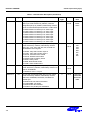
Table 1-1. S3CC410 Pin Description (Continued)
Circuit
Type
Number
Shared
Pins
Not external SRAM output enable
–
159
–
O
Not external SRAM write enable
–
160
–
NCAS
O
Not external DRAM column address strobe
–
149
–
NRAS
O
Not external DRAM row address strobe
–
153
–
NDCS
O
Not external DRAM chip select
–
151
–
NDWE
O
Not external DRAM write enable
–
152
–
CKE
O
External DRAM clock enable
–
161
–
DQM
O
External DRAM data input/output mask
–
162
–
BA.0-BA.1
O
External DRAM bank select address
–
147-148
–
ICLK
O
Internal system clock output
–
164
–
AVREF
I
Reference voltage for A/D converter
–
35
–
BKREQX
I
External break request
–
99
–
NGIDISX
I
Not External global interrupt disable
–
100
–
NTRST
I
Not test reset input for TAP controller; Alternatively
used as state initialization input in serial mode
–
101
UINIT
TCKMCLK
I
TAP controller test clock input
–
102
–
TDIRXD
I
TAP controller test data input; Alternatively used as
received data input in serial mode
–
103
RXD
JTAGSEL
I
JTAG interface mode selection
–
104
–
TMS
I
TAP controller test mode selection
–
105
–
UCLK
I
UART clock input
–
106
–
EVBP
O
Combinational event match indication
–
107
–
RUNST
O
Run-state indication
–
108
–
TDOTXD
O
TAP controller test data output; Alternatively used as
transmitted data output in serial mode
–
109
TXD
EXTBK.0EXTBK.3
I
External event match enable
–
111-114
–
EVMAT.0EVMAT.3
O
Event match from 4-event channel
–
115-118
–
NEXPACK
O
Not exception acknowledge
–
145
–
TMODE
I
Test mode selection
–
146
–
NRESET
I
Not global reset input
–
143
–
NRESETO
I
Not system reset output
–
144
–
1-8
Name
Type
NSOE
O
NSWE
Description
S3CC410 (Preliminary Spec)
PRODUCT OVERVIEW
Table 1-1. S3CC410 Pin Description (Continued)
Name
Type
CP0
–
CZ0
Description
Circuit
Type
Number
Shared
Pins
Loop filter VCO input for PLL 0
–
39
–
–
Loop filter pump output for PLL0
–
40
–
CP1
–
Loop filter VCO input for PLL 1
–
43
–
CZ1
–
Loop filter pump output for PLL1
–
44
–
VDD
–
Global power supply
–
7, 22,
53, 68,
83, 98,
121,135,
150,163,
176,188,
210
–
VSS
–
Global ground
–
14, 28,
60, 76,
90, 110,
127,141,
157,170,
182,195,
208
–
VDD_ADC
–
Power supply for A/D converter
–
33
–
VSS_ADC
–
Ground for A/D converter
–
34
–
VDD_USB
–
Power supply for USB
–
36
–
VSS_USB
–
Ground for USB
–
37
–
VDD_PLL0
–
Power supply for PLL 0
–
38
–
VSS_PLL0
–
Ground for PLL 0
–
41
–
VDD_PLL1
–
Power supply for PLL 1
–
42
–
VSS_PLL1
–
Ground for PLL 1
–
45
–
1-9
PRODUCT OVERVIEW
S3CC410 (Preliminary Spec)
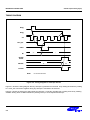
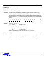
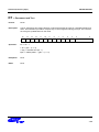
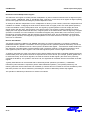
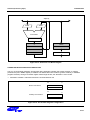
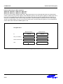
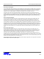
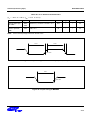
PIN CIRCUIT DIAGRAMS
Select
VDD
Port Data
Alternative Signal
M
U
X
Data
In/Out
Output Disable
Alternative Input
VSS
Normal Input
Figure 1-3. Pin Circuit Type 1 (Port 0, P1.0-P1.4, P6.0-P6.5, and Port 7)
VDD
Pull-up
Resistor
Pull-up Enable
Select
VDD
Port Data
Alternative Signal
M
U
X
Data
In/Out
Output Disable
Alternative Input
VSS
Normal Input
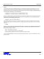
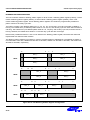
Figure 1-4. Pin Circuit Type 2 (P6.6 and P6.7)
1-10
S3CC410 (Preliminary Spec)
PRODUCT OVERVIEW
VDD
Pull-up
Resistor
Pull-up Enable
Select
VDD
Port Data
Alternative Signal
M
U
X
Data
In/Out
Output Disable
Alternative Input
VSS
Normal Input
Figure 1-5. Pin Circuit Type 3 (P4.2)
1-11
PRODUCT OVERVIEW
S3CC410 (Preliminary Spec)
Select
VDD
Port Data
Alternative Signal
M
U
X
Data
In/Out
Output Disable
Alternative Input
VSS
Normal Input
Figure 1-6. Pin Circuit Type 4 (Port 2, Port 8, Port 9, and Port 10)
VDD
Pull-up
Resistor
Pull-up Enable
Select
VDD
Port Data
Alternative Signal
M
U
X
Data
In/Out
Open-Drain
Output Disable
Alternative Input
VSS
Normal Input
Figure 1-7. Pin Circuit Type 5 (Port 3)
1-12
S3CC410 (Preliminary Spec)
PRODUCT OVERVIEW
VDD
Pull-up
Resistor
Pull-up Enable
VDD
Data
In/Out
Output Disable
Input
VSS
Noise
Filter
External
Interrupt Input
Figure 1-8. Pin Circuit Type 6 (P4.0, and P4.1)
VDD
Pull-up
Resistor
Pull-up Resistor
Enable
Normal Input Mode
Normal Input
Interrupt Input
Noise
Filter
A/D C Logic
+
-
In
VREF
Figure 1-9. Pin Circuit Type 7 (Port 5)
1-13
PRODUCT OVERVIEW
S3CC410 (Preliminary Spec)
VDD
In
Figure 1-10. Pin Circuit Type 8 (RESET
RESET)
In
Figure 1-11. Pin Circuit Type 9 (TEST)
1-14
S3CC410 (Preliminary Spec)
2
ADDRESS SPACE
ADDRESS SPACE
OVERVIEW
CalmRISC16 has 21-bit program address lines, PA[20:0], which supports up to 2M word of program memory.
The 2M word program memory space is divided into 8-kword internal program memory and instruction cache memory
area.
CalmRISC16 also has 22-bit data memory address lines, DA[21:0], which supports up to 4M byte.
The 4M byte data memory space is divided into 72K byte internal data memory and data cache memory area.
Memory configuration in CalmRISC16 side
Data Memory:
4K byte data cache
72K byte internal data memory
Code Memory:
4K byte instruction cache
8K word internal program memory
Memory configuration in CalmMAC24 side
Data Memory:
X-Memory area - 16K word internal memory (48K byte)
Y-Memory area - 8K word internal memory (24K byte)
Code Memory:
4K byte instruction cache
8K word internal program memory
2-1
ADDRESS SPACE
S3CC410 (Preliminary Spec)
PROGRAM MEMORY
Program memory configuration is shown in Figure 2-1. If PA of CalmRISC16 is higher than 3FBFFFH, the program
data is supported from the internal program memory. And if PA of CalmRISC16 is lower than 3FC000H, the program
data is supported from instruction cache controller.
3FFFFFH
Internal Program Memory
3FC000H
Chcheable Area
000000H
Byte
Figure 2-1. Program Memory Configuration
2-2
S3CC410 (Preliminary Spec)
ADDRESS SPACE
DATA MEMORY
Data memory configuration is shown in Figure 2.2. CalmMAC24 only can access the internal data memory and if the
memory request tries to access non-existent memory area, FIQ(Fast Interrupt request) is generated. In this case, if
FE bit in CalmRISC16’s SR register is 1, the violation service routine is called and served. CalmRISC16 can access
the internal data memory and data cache area. If DA[21] of CalmRISC16 is 1, the internal memory is accessed. And
if DA[21] of CalmRISC16 is 0, the data cache controller is accessed.
The memory violation( access the non-existent area ) FIQ can be also generated.
3FFFFFH
I/O Area
3F0000H
YMX1
YMX0
YMH1
YML1
YMH0
YML0
234000H
232000H
230000H
224000H
222000H
220000H
218000H
XMX
210000H
208000H
XMH
XML
200000H
Chcheable Area
000000H
Byte
Figure 2-2. Data Memory Configuration
2-3
ADDRESS SPACE
S3CC410 (Preliminary Spec)
EXTERNAL OFF-CHIP MEMORY
CalmRISC16 can only see the 2-M word program memory and 4-M byte data memory. CalmMAC24 can only see the
2-M word program memory and 64-K word data memory (192-K byte). But we designed S3CC410 to attach
maximum 16-M word memory(8-M word SRAM + 8-M word SDRAM). The larger physical memory than address
space is supported by instruction cache, data cache and DMA. The ICBASE register in instruction cache controller
is used as the base pointer to access external off-chip memory in program memory request. And the DCBASE
register in data cache controller is used as the base pointer to access external off-chip memory in data memory
request. By changing the value of ICBASE or DCBASE register, we can access the whole 16M-word off-chip
memory. Also DMA (DDMA, YDMA) can transfer data between internal memories and external off-chip memory.
The external memory configuration of S3CC410 is shown in Figure 2-3. The lower half of the memory space is only
used for SRAM, and the higher half is only used for SDRAM. The SRAM bank size is varies from 256K-word to 2Mword.
SRAM Bank Size
= 256K word
SRAM Bank Size
= 2M word
Bank 0
Bank 1
Bank 2
Bank 0
Bank 3
SRAM
(8M words)
Bank 1
Bank 0
Unused
Bank 0
Bank 2
Bank 1
SDRAM
(8M word)
Bank 1
Bank 2
Bank 2
Bank 3
Bank 3
Bank 3
SDRAM
Bank Size
= 2M word
Figure 2-3. External Off-Chip Memory Space Configuration
2-4
S3CC410 (Preliminary Spec)
3
CALM16CORE
CALM16CORE
INTRODUCTION
The main features of CalmRISC16, a 16-bit embedded RISC MCU core, are high performance, low power
consumption, and efficient coprocessor interface. It can operate up to 100MHz, and consumes 100µA/MHz @3.3V.
When operating with MAC2424, a 24-bit fixed point DSP coprocessor, CalmRISC16 can operate up to 80MHz.
Through efficient coprocessor interface, CalmRISC16 provides a powerful and flexible MCU+DSP solution. The
following gives brief summary of main features of CalmRISC16.
FEATURES
H/W Feature
Instruction Set
•
Power consumption: 100µA per MHz @3.3V,
0.35µ process
•
16-bit instruction width for 1-word instructions
•
32-bit instruction width for 2-word instructions
•
Maximum frequency: 100MHz @3.3V
•
Load/Store instruction architecture
•
0.78 mm2 die size
•
Delayed branch support
Architecture
•
C-language/OS support
•
Harvard RISC architecture
•
Bit operation for I/O process
•
5-Stage pipeline
Instruction Execution Time
Registers
•
•
Sixteen 16-bit general registers
Address Space
•
Eight 6-bit extension registers
•
4M byte for Program Memory
•
22-bit Program Counter (PC)
•
4M byte for Data Memory
•
16-bit Status Register (SR)
•
Seven saved registers for interrupts.
One instruction/cycle for basic instructions
3-1
CALM16CORE
S3CC410 (Preliminary Spec)
REGISTERS
In CalmRISC16 there are sixteen 16-bit general registers, eight 6-bit extension registers, a 16-bit Status
Register(SR), a program counter (PC), and five saved registers.
GENERAL REGISTERS & EXTENSION REGISTERS
The following figure shows the structure of the general registers and the extension registers.
16-bit
22-bit
R0
PC
R1
SPC_FIQ
.
.
.
Registers for Byte
SPC_IRQ
SR
R7
Address Registers
SSR_FIQ
E8
R8
E9
R9
.
.
.
.
.
.
E14
R14
Link Register
E15
R15
Stack Pointer
SSR_IRQ
SSR_SWI
16-bit
22-bit
Figure 3-1. Register Structure in CalmRISC16
The general registers (from R0 to R15) can be either a source register or a destination register for almost all ALU
operations, and can be used as an index register for memory load/store instructions (e.g., LDW R3, @[A8+R2]). The
6-bit extension registers (from E8 to E15) are used to form a 22-bit address register (from A8 to A15) by
concatenating with a general register (from R8 to R15). The address registers are used to generate 22-bit program
and data addresses.
3-2
S3CC410 (Preliminary Spec)
CALM16CORE
SPECIAL REGISTERS
The special registers consist of 16-bit SR (Status Register), 22-bit PC (Program Counter), and saved registers for
IRQ(interrupt), FIQ(fast interrupt), and SWI(software interrupt). When IRQ interrupt occurs, the most significant 6 bits
of the return address are saved in SPCH_IRQ, the least significant 16 bits of the return address are saved in
SPCL_IRQ, and the status register is saved in SSR_IRQ. When FIQ interrupt occurs, the most significant 6 bits of
the return address are saved in SPCH_FIQ, the least significant 16 bits of the return address are saved in
SPCL_FIQ, and the status register is saved in SSR_FIQ. When a SWI instruction is executed, the return address is
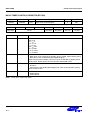
saved in A14 register (E14 concatenated with R14), and the status register is saved in SSR_SWI. The least
significant bit of PC, SPCL_IRQ and SPCL_FIQ is read only and its value is always 0.
— The 16-bit register SR has the following format.
15
T
–
–
–-
–
–
–
8
7
–
–
0
PM
Z1
Z0
V
TE
IE
FE
•
FE: FIQ enable bit, FIQ is enabled when FE is set.
•
IE: IRQ enable bit, IRQ is enabled when IE is set.
•
TE: TRQ enable bit, Trace is enabled when TE is set.
•
V: overflow flag, set/clear accordingly when arithmetic instructions are executed.
•
Z0: zero flag of R6, set when R6 equals zero and used as the branch condition when BNZD instruction with R6 is
executed.
•
Z1: zero flag of R7, set when R7 equals zero and used as the branch condition when BNZD instruction with R7 is
executed.
•
PM: privilege mode bit. PM = 1 for privilege mode and PM = 0 for user mode
•
T: true flag, set/clear as a result of an ALU operation.
FE, IE, TE, and PM bits can be modified only when PM = 1 (privilege mode). The only way to change from user
mode to privilege mode is via interrupts including SWI instructions. The reserved bit of SR (from bit 7 to bit 14) can be
used for other purposes without any notice. Hence programmers should not depend on the value of the reserved bits
in their programming. The reserved bits are read as 0 value.
3-3
CALM16CORE
S3CC410 (Preliminary Spec)
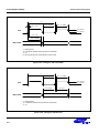
PIPELINE STRUCTURE
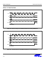
CalmRISC16 has a 5-stage pipeline architecture. It takes 5 cycles for an instruction to do its operation. In a pipeline
architecture, instructions are executed overlapped, hence the throughput is one instruction per cycle. Due to data
dependency, control dependency, and 2 word instructions, the throughput is about 1.2 on the average. The following
diagram depicts the 5-stage pipeline structure.
IF
ID
EX
MEM
WB
In the first stage, which is called IF (Instruction Fetch) stage, an instruction is fetched from program memory. In the
second stage, which is called ID (Instruction Decoding) stage, the fetched instruction is decoded, and the
appropriate operands, if any, for ALU operation are prepared. In the case of branch or jump instructions, the target
address is calculated in ID stage. In the third stage, which is called EX (Execution) stage, ALU operation and data
address calculation are executed. In the fourth stage, which is called MEM (Memory) stage, data transfer from/to
data memory or program memory is executed. In the fifth stage, which is called WB (Write Back) stage, a write-back
to register file can be executed. The following figure shows an example of pipeline progress when 3 consecutive
instructions are executed.
I1 : ADD R0, 3
I2 : ADD R1, R0
I3 : LD R2, R0
IF
ID
EX
MEM
WB
IF
ID
EX
MEM
WB
IF
ID
EX
MEM
WB
In the above example, the instruction I2 needs the result of the instruction I1 before I1 completes. To resolve this
problem, the EX stage result of I1 is forwarded to ID stage of I2. Similar forwarding mechanism occurs from MEM
stage of I1 to ID stage of I3.
The pipeline cannot progress (called a pipeline stall) due to a data dependency, a control dependency, or a resource
conflict.
When a source operand of an ALU instruction is from a register, which is loaded from memory in the previous
instruction, 1 cycle of pipeline stall occurs (called load stall). Such load stalls can be avoided by smart reordering of
the instruction sequences. CalmRISC16 has 2 classes of branch instructions, those with a delay slot and without a
delay slot. Non-delay slot branch instructions incurs a 1 cycle pipeline stall if the branch is taken, due to a control
dependency. For branch instructions with a delay slot, no cycle waste is incurred if the delay slot is filled with a
useful instruction (or non NOP instruction). Pipeline stalls due to resource conflicts occurs when two different
instructions access at the same cycle the same resource such as the data memory and the program memory. LDC
(data load from program memory) instruction causes a resource conflict on the program memory. Bit operations such
as BITR and BITS (read-modify-write instructions) cause a resource conflict on the data memory.
3-4
S3CC410 (Preliminary Spec)
CALM16CORE
INTERRUPTS
In CalmRISC16, there are five interrupts: RESET, FIQ, IRQ, TRQ, SWI. The RESET, FIQ, and IRQ interrupts
correspond to external requests. TRQ and SWI interrupts are initiated by an instruction (therefore, in a deterministic
way). The following table shows a summary of interrupts.
Name
Priority
Address
Description
RESET
1
000000h
Hardware Reset
FIQ
3
000002h
Fast Interrupt Request
IRQ
5
000004h
Interrupt Request
TRQ
2
000006h
Trace Request
SWI
4
000008h–
0000feh
Software Interrupt
When nRES (an input pin CalmRISC16 core) signal is released (transition from 0 to 1), “JMP addr:22” is
automatically executed by CalmRISC16. Among the 22-bit address addr:22, the most significant 6 bits are forced to
0, and the least significant 16 bits are the contents of 000000h (i.e., reset vector address) of the program memory.
In other words, “JMP {6’h00, PM[000000h]}” instruction is forced to the pipeline. The initial value of PM bit is 1 (that
is, in privilege mode) and the initial values of other bits in SR register are 0. All other registers are not initialized (i.e.,
unknown).
When nFIQ (an input pin CalmRISC16 core) signal is active (transition from 1 to 0), “JMP addr:22” instruction is
automatically executed by CalmRISC16. The address of FIQ interrupt service routine is in 000002h (i.e., FIQ vector
address) of the program memory (i.e., “JMP {6’h00, PM[000002h]}”). The return address is saved in {SPCH_FIQ,
SPCL_FIQ} register pair, and the SR value is saved in SSR_FIQ register. PM bit is set. FE, IE, and TE bits are
cleared. When RET_FIQ instruction is executed, SR value is restored from SSR_FIQ, and the return address is
restored into PC from {SPCH_FIQ, SPCL_FIQ}.
When nIRQ signal (an input pin CalmRISC16 core) is active (transition from 1 to 0), “JMP {6’h00, PM[000004h]}”
instruction is forced to the instruction pipeline. The return address is saved in {SPCH_IRQ, SPCL_IRQ} register pair,
and the SR value is saved in SSR_IRQ register. PM bit is set. IE and TE bits are cleared. When RET_IRQ instruction
is executed, SR value is restored from SSR_IRQ, and return address is restored to PC from {SPCH_IRQ,
SPCL_IRQ}.
When TE bit is set, TRQ interrupt happens and “JMP {6’h00, PM[000006h]}” instruction is executed right after each
instruction is executed. TRQ interrupt uses the saved registers of IRQ(that is, {SPCH_IRQ, SPCL_IRQ} register pair
and SSR_IRQ) to save the return address and SR, respectively. PM bit is set. IE, TE bits are cleared.
When “SWI imm:6” instruction is executed, the return address is saved in the register A14, and the value of SR is
saved in SSR_SWI. Then the program sequence jumps to the address (imm:6 * 4). PM bit is set. IE and TE bits are
cleared. “SWI 0” and “SWI 1” are prohibited because the addresses are reserved for other interrupts. When RET_SWI
instruction is executed, SR is restored from SSR_SWI, and the return address is restored to PC from A14.
NOTES:
1. 6’h00 is defined as 00 (or zero) in 6 bits
2. imm:6 is defined as 6-bit immediate number
3-5
CALM16CORE
S3CC410 (Preliminary Spec)
MEMORY FORMATS
CalmRISC16 adopts a big endian memory format. In a big endian memory format, the most significant byte of word
data is stored at an even address, and the least significant byte is stored at an odd address. For example let us
assume that the word data “1234h” is stored at the address 100h. Then the higher byte “12h” is stored at the address
100h, and the lower byte “34h” is stored at the address 101h. When the 22-bit data “123456h” is stored at the
address 100h by “LDW @An, Ai” instruction, “00h” is at the address 100h, “12h” is at the address 101h, “34h” is at
the address 102h, and “56h” is at the address 103h.
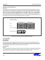
SIGNAL DESCRIPTION
Table 3-1. Signal Description
3-6
Name
Direction
Description
PA[20:0]
O
PD[15:0]
I
nPMCS
O
Program Memory Chip Selection
nLDC
O
Data load from program memory indicator
DA[21:0]
O
Data Memory Address
DA[4:0] is shared with SYS and CLD instructions
DI[15:0]
I
Input from Data Memory, Input from coprocessor for CLD instruction.
DO[15:0]
O
Output to Data Memory, Output to coprocessor for CLD instruction.
nDMCSH
O
Chip Selection for Higher Byte Data Memory
nDMCSL
O
Chip Selection for Lower Byte Data Memory
DMWR
O
Data Memory Write, 1 means transfer from Core to Memory
nDME
O
Data Bus Enable Signal.
nRES
I
Hardware Reset
nFIQ
I
Fast Interrupt Request
nIRQ
I
Interrupt Request
nEXPACK
O
nWAIT
I
nSYSID
O
MCLK
I
ECLK
O
Early Clock Output
ICLK
O
Clock Output
nCOPID
O
Coprocessor instruction indicator
nCLDID
O
Coprocessor Load instruction indicator
Program Memory Address, equivalent to PC[21:1]
Program Data
Exception Acknowledge
Wait signal, core is stopped when active.
SYS instruction indicator
Main Clock Input
S3CC410 (Preliminary Spec)
CALM16CORE
Table 3-1. Signal Description (Continued)
Name
Direction
Description
CLDWR
O
Write to Coprocessor indicator
COPIR[12:0]
O
Instruction to coprocessor, 13-bit immediate field in COP instruction.
EC[3:0]
I
nBRK
O
Software break indicator
nBKACK
O
Break Acknowledge
BKMODE[2:0]
O
Break Mode, indicates core state when core breaks.
BKREQ
I
Break Request
nGIDIS
I
Global interrupt disable, when active, all interrupt is disabled.
PDGRANT
I
Indicates program memory access is permitted.
PDWAIT
I
Indicates current program memory access is not complete.
DBGRANT
I
Indicates data memory access is permitted.
DBWAIT
I
Indicates current data memory access is not complete.
DBREQ
O
Signal asking for data bus permission.
PMODE
O
Privilege Mode Indicator
CGRANT
O
Indicates that coprocessor may use data bus.
CSTALL
I
Coprocessor indicates that coprocessor pipeline stall occurs.
CMW
I
Coprocessor indicates that coprocessor instruction is multiple word.
nSEQ
O
nINCPC
I
CCLK
O
External Conditions from coprocessor or peripherals.
Indicates that the next program address is sequential.
If it is 1, PC value is not incremented when sequential execution.
Clock output to coprocessor
3-7
CALM16CORE
S3CC410 (Preliminary Spec)
NOTES
3-8
S3CC410 (Preliminary Spec)
4
EXCEPTIONS
EXCEPTIONS
OVERVIEW
Exceptions in CalmRISC16 are listed in the table below. Exception handling routines, residing at the given addresses
in the table, are invoked when the corresponding exception occurs. The starting address of each exception routine is
specified by concatenating 0H (leading 4 bits of 0) and the 16-bit data in the exception vector listed in the table. For
example, the interrupt service routine for FIQ starts from 0H:PM[000002H]. Note that “:” means concatenation and
PM[*] stands for the 16-bit content at the address * of the program memory. When an IRQ or FIQ occurs, current PC
is pushed in the SPC_IRQ, SPC_FIQ on an exception. And if SWI is executed, current PC is pushed in the E14:R14
register.
Table 4-1. Exceptions
Name
Address
Priority
Reset
000000H
1 st
Exception due to reset release.
FIQ
000002H
3 rd
Exception due to nFIQ signal..Maskable by setting FE
IRQ
000004H
5 th
Exception due to nIRQ signal. Maskable by setting IE
TRQ
000006H
2 nd
Exception due to TE bit in SR register
SWI
000008H–
0000FEH
4 th
Exception due to SWI execution
NOTE:
Description
Break mode due to BKREQ has a higher priority than all the exceptions above. That is, when BKREQ is active,
even the exception due to reset release is not executed.
HARDWARE RESET
When nRES (an input pin CalmRISC16 core) signal is released (transition from 0 to 1), “JMP addr:22” is
automatically executed by CalmRISC16. Among the 22-bit address addr:22, the most significant 6 bits are forced to
0, and the least significant 16 bits are the contents of 000000h (i.e., reset vector address) of the program memory.
In other words, “JMP {6’h00, PM[000000h]}” instruction is forced to the pipeline. The initial value of PM bit is 1 (that
is, in privilege mode) and the initial values of other bits in SR register are 0. All other registers are not initialized (i.e.,
unknown).
4-1
EXCEPTIONS
S3CC410 (Preliminary Spec)
FIQ EXCEPTION
When nFIQ (an input pin CalmRISC16 core) signal is active (transition from 1 to 0), “JMP addr:22” instruction is
automatically executed by CalmRISC16. The address of FIQ interrupt service routine is in 000002h (i.e., FIQ vector
address) of the program memory (i.e., “JMP {6’h00, PM[000002h]}”). The return address is saved in {SPCH_FIQ,
SPCL_FIQ} register pair, and the SR value is saved in SSR_FIQ register. PM bit is set. FE, IE, and TE bits are
cleared. When RET_FIQ instruction is executed, SR value is restored from SSR_FIQ, and the return address is
restored into PC from {SPCH_FIQ, SPCL_FIQ}.
IRQ EXCEPTION
When nIRQ signal (an input pin CalmRISC16 core) is active (transition from 1 to 0), “JMP {6’h00, PM[000004h]}”
instruction is forced to the instruction pipeline. The return address is saved in {SPCH_IRQ, SPCL_IRQ} register pair,
and the SR value is saved in SSR_IRQ register. PM bit is set. IE and TE bits are cleared. When RET_IRQ instruction
is executed, SR value is restored from SSR_IRQ, and return address is restored to PC from {SPCH_IRQ,
SPCL_IRQ}.
TRQ EXCEPTION
When TE bit is set, TRQ interrupt happens and “JMP {6’h00, PM[000006h]}” instruction is executed right after each
instruction is executed. TRQ interrupt uses the saved registers of IRQ(that is, {SPCH_IRQ, SPCL_IRQ} register pair
and SSR_IRQ) to save the return address and SR, respectively. PM bit is set. IE, TE bits are cleared.
SWI EXCEPTION
When “SWI imm:6” instruction is executed, the return address is saved in the register A14, and the value of SR is
saved in SSR_SWI. Then the program sequence jumps to the address (imm:6 * 4). PM bit is set. IE and TE bits are
cleared. “SWI 0” and “SWI 1” are prohibited because the addresses are reserved for other interrupts. When RET_SWI
instruction is executed, SR is restored from SSR_SWI, and the return address is restored to PC from A14.
BREAK EXCEPTION
Break exception is reserved only for an in-circuit debugger. When a core input signal, BKREQ, is high, the
CalmRISC16 core is halted or in the break mode, until BKREQ is deactivated. Another way to drive the CalmRISC16
core into the break mode is by executing a break instruction, BREAK. When BREAK is fetched, it is decoded and
the CalmRISC16 core output signal nBKACK is generated. An in-circuit debugger generates BKREQ active by
monitoring nBKACK to be active. BREAK instruction is exactly the same as the NOP (no operation) instruction
except that it does not increase the program counter and activates nBKACK. There, once BREAK is encountered in
the program execution, it falls into a deadlock. BREAK instruction is reserved for in-circuit debuggers only, so it
should not be used in user programs.
NOTE:
4-2
imm:6 is defined as 6-bit immediate number
S3CC410 (Preliminary Spec)
EXCEPTIONS
FIQ Sources
The FIQ in S3CC410 is generated when several violations occur. The violated conditions are as follows.
— Access to data memory area not exist
— Access to IO space not exist ( higher than 3F018FH )
— Access to IO space in USER Mode
Any condition of these three cases matches, nIFQ to the CalmRISC16 is activated. If the FE bit in SR is 1, then FIQ
routine is called and executed.
INTERRUPT SOURCES (IRQ)
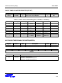
The ICU(Interrupt Control Unit) can manage 32 interrupt sources and 28-interrupt sources are implemented in
S3CC410. The details are described in the section ICU.
Interrupt Name
Interrupt Type
ICU0
ICU1
IRQ0
BT INT
EXT INT 0 (P5[0])
IRQ1
RTC INT
EXT INT 1 (P5[1])
IRQ2
TA INT
EXT INT 2 (P5[2])
IRQ3
TAOV INT
EXT INT 3 (P5[3])
IRQ4
TB INT
EXT INT 4 (P5[4])
IRQ5
TBOV INT
EXT INT 5 (P5[5])
IRQ6
TC INT
EXT INT 6 (P5[6])
IRQ7
TCOV INT
EXT INT 7 (P5[7])
IRQ8
USB INT
EXT INT8 (P4[0])
IRQ9
PPIC INT
EXT INT9 (P4[1])
IRQ10
UART_Rx/UART_Err/UART_tx INT
–
IRQ11
IIC INT
DDMA INT
IRQ12
SIO INT
YDMA INT
IRQ13
IIS0 INT
LCD INT
IRQ14
IIS1 INT
–
IRQ15
–
–
4-3
EXCEPTIONS
S3CC410 (Preliminary Spec)
MINIMIZING INTERRUPT LATENCY MODE (IRQ)
In general, there are many interrupt sources to make interrupt request signals. So as soon as interrupt service
routine is called, we must identify the interrupt source to serve the request. In other word, we must read the IIR
register in ICU and manipulate it then jump to the corresponding service routine by referencing the value. These
sequences increase the interrupt latency and make system performance lower. In S3CC410, there is special mode
to minimize interrupt latency, which we call MIL mode. In this mode, lower 64-bytes in internal program memory is
used to store interrupt service routine address. When nEXPACK is activated, the program data is supported from
internal program memory corresponding to the IIR value from the ICU. So if you use this MIL mode, you must make
the interrupt service routine address table in the internal program memory. And you must set the bit 0 in INTMODE
register of which located at 3F010CH. The MIL scheme is shown in Figure 4-1.
3FFFFFH
PA
CalmRISC16
{8'h00,IIR}
ICU
~nEXPACK &
(PA[1:0]==10)
Internal
Program
Memory
3FC040H
Interrupt
Table
Figure 4-1. Minimizing Interrupt Latency mode
4-4
3FC000H
S3CC410 (Preliminary Spec)
5
INTERRUPT CONTROL UNIT
INTERRUPT CONTROL UNIT
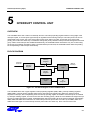
OVERVIEW
The CalmRISC16ICU has a total of 32 interrupt sources. The interrupt pending register catches a rising-edge of the
interrupt request, so a short pulse type interrupt is regarded as the meaning interrupt. The interrupt sources can be
categorized to two groups, the group of the higher priority (from index 0 to index 15) and the group of the lower
priority (from index 16 to index 31). It’s flexible to change the priority between interrupt sources belonged to the same
group. When some interrupts are enabled simultaneously, the CalmRISC16ICU resolves the only one of them using
the priority and masking information. When a resolved interrupt is serviced, the CalmRISC16ICU clears the pending
bit corresponding to the interrupt automatically.
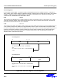
BLOCK DIAGRAM
Interrupt
Sources
Interrupt
Masking
Register
Interrupt
Pending
Register
Priority
Resolving
Logic
Global
Interrupt
Interrupt
Priority
Register
Auto-clear
Logic
Interrupt
ID
Register
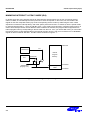
Figure 5-1. The Block Diagram of the CalmRISC16ICU
The CalmRISC16ICU has 4-types registers: interrupt pending registers (IRQ0, IRQ1), interrupt masking registers
(IMR0, IMR1), interrupt priority registers (IPR0, IPR1) and interrupt ID register (IIR). When any interrupt source
requests an interrupt, the corresponding bit of the interrupt pending register is enabled. If the interrupt is not masked
by interrupt masking register, it’s send to the core after checking priority. While the core identifies the target interrupt
source by reading interrupt ID register, CalmRISC16ICU clears the pending bit of the serviced interrupt automatically.
IRQ0, IMR0 and IPR0 control the lower 16 of the interrupt sources (from index 0 to index 15) and IRQ1, IMR1 and
IPR0 control the higher 16 of the interrupt sources (from index 16 to index 31). IIR is common to the both.
5-1
INTERRUPT CONTROL UNIT
S3CC410 (Preliminary Spec)
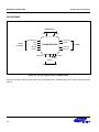
PIN DIAGRAM
Global Signal
CLK
nRES
SELREG[2:0]
nWR
to PeriController
nRD
nCLK_INT
nIACK
CalmRISC16ICU
to CORE
BYTEH
DO[15:0]
BYTEL
DI[15:0]
IRQI[31:0]
WAKEUP
nCLRIID
IID[4:0]
to Interrupt Sources
Figure 5-2. The pin diagram of the CalmRISC16ICU
Figure 5-2 shows the inputs and the outputs of the CalmRISC16ICU. CalmRISC16ICU has a total of 58 inputs and 24
outputs.
5-2
S3CC410 (Preliminary Spec)
INTERRUPT CONTROL UNIT
Table 5-1. Signal Description of the CalmRISC16ICU
Signal
I/O
Descriptions
nRES
I
Global RESET signal(negative enable)
CLK
I
Global Clock signal
SELREG[2:0]
I
Register selection signal :
IRQ0, IMR0, IPR0, IIR, IRQ1, IMR1, IPR1, IIR (increasing order, from 0 to 7).
Especially, IIR can be selected by index 3 and index 7.
nWR
I
Write enable signal(negative enable)
nRD
I
Read enable signal(negative enable)
BYTEH
I
Enable signal for the high byte in reading/writing.
BYTEL
I
Enable signal for the low byte in reading/writing.
nCLK_INT
O
Interrupt to the core in the 2nd phase of the clock (negative enable).
nIACK
I
Acknowledge signal from the core (negative enable).
DI[15:0]
I
Data input (in reading a register).
DO[15:0]
O
Data output (in writing a register).
IRQI[31:0]
I
Interrupt Sources.
IID[4:0]
O
The ID of the current serviced interrupt. If “nCLK_INT” is disabled, IID is
meaningless.
nCLRIID
O
When the core reads the IIR register or clears all interrupt, nCLRIID is set
(negative).
WAKEUP
O
Any unmasked interrupt causes to enable “WAKEUP”.
To read/write a register, “BYTEH” or “BYTEL” signal must be enabled.
5-3
INTERRUPT CONTROL UNIT
S3CC410 (Preliminary Spec)
INTERRUPT CONTROL REGISTERS
The CalmRISC16ICU has 4-types, 7 registers. All registers except interrupt ID register consist of two 16-bit registers.
The lower word is named to register0 and the higher word is named to register1. It’s possible to access not only the
word but also the byte of each register.
INTERRUPT PENDING REGISTER
It consists of two 16-bits registers IRQ0 and IRQ1 (IRQ1 is an interrupt pending register for interrupt sources [31:16]).
Interrupt pending register can be set by the rising-edge of the interrupt sources or by “write” command of the core.
You can clear the pending interrupt as the followings. It needs to identify the ID of interrupt source when any interrupt
is occurred. To do this, interrupt service routine must read the IIR. CalmRISC16ICU clears the bits of interrupt
pending register corresponding to the “IIR” value automatically during IIR is being read. If you want to clear any
pending interrupt intentionally, write the index of pending interrupt to “IIR” register. The latter method is described in
the section “Interrupt ID Register”. The core can not clear the pending interrupt by writing ‘0000’ to IRQ registers.
INTERRUPT MASKING REGISTER
It consists of two 16-bits registers IMR0 and IMR1 (IMR1 is an interrupt masking register for interrupt sources
[31:16]). The role of IMR masks the pending interrupt. Although any interrupt source sets the interrupt pending
register, the interrupt cannot be send to the core if the interrupt is masked.
0: mask (default value)
1: unmask
For example, if you want to pass only 5, 8 and 15th interrupt sources, you have to load the value “8120h” to the
“IMR0” register. “IMR0” and “IMR1” have initial value “0000”(all masking).
INTERRUPT PRIORITY REGISTER
It consists of two registers IPR0 and IPR1 (IPR1 is an interrupt priority register for interrupt sources [31:16]). Two
registers determine the serving order of interrupts when any interrupts of 32 sources occur simultaneously. The
priority of the interrupt sources is determined as following. For convenience, the interrupt sources can be grouped to
4 bytes: IRQI3, IRQI2, IRQI1, IRQI0 (from index 31 to index 24, from index 23 to index 16, from index 15 to index 8
and from index 7 to index 0)
1.
The interrupt sources with the lower indices (IRQI1 and IRQI0) are prior to the others (IRQI3 and IRQI2).
2.
The interrupts of IRQI1 and IRQI0 are generated by the order described in 13-bits register, IPR0. The lower 8 bits
of IPR0 can define the order of the both IRQI1 and IRQI0 as shown in figure 3. If you define the order of IRQI1 as
following: 15 < 14 < … < 8, the order of IRQ0 is defined as 7 < 6 < … < 0. The default value is “10h” which the
order is defined as decreasing order: 7 < 6 < … < 0. The higher 5 bits of IPR0 define the priority between the
subgroups of IRQI1 and IRQI0. Each subgroup can be shuffled as shown in figure 3.
3.
The priority in IRQI3 is not variable. Always the interrupts is ordered as:
23 < 22 < 21 < 20 < 19 < 18 < 17 < 16
4.
The priority in IRQI4 is controlled by IPR1, 8-bits register. IPR1 is same as the lower 8-bits of IPR0. Also the
default priority of IRQI4 is a decreasing order.
5-4
S3CC410 (Preliminary Spec)
INTERRUPT CONTROL UNIT
Interrupt Priority Register (IPR)
.4
.3
.2
.1
.0
xx000: X0>Y0>Z0>X1>Y1>Z1
x0100: X0>Y0>X1>Z0>Y1>Z1
01100: X0>Y0>X1>Y1>Z0>Z1
11100: X0>Y0>X1>Y1>Z1>Z0
x0010: X0>X1>Y0>Z0>Y1>Z2
00110: X0>X1>Y1>Y0>Z0>Z1
10110: X0>X1>Y1>Y0>Z1>Z0
01010: X0>Y1>Y0>Y1>Z0>Z1
11010: X0>X1>Y0>Y1>Z1>Z0
x1110: X0>X1>Y1>Z1>Y0>Z0
xx001: X1>Y1>Z1>X0>Y0>Z0
x0101: X1>Y1>X0>Z1>Y0>Z0
01101: X1>Y1>X0>Y0>Z1>Z0
11101: X1>Y1>X0>Y0>Z0>Z1
x0011: X1>X0>Y1>Z1>Y0>Z0
00111: X1>X0>Y0>Y1>Z1>Z0
10111: X1>X0>Y0>Y1>Z0>Z1
01011: X1>X0>Y1>Y0>Z1>Z0
11011: X1>X0>Y1>Y0>Z0>Z1
X1111: X1>X0>Y0>Z0>Y1>Z1
MSB
.7
.6
.5
.4
.3
.2
.1
.0
Group priority:
Group A
0 = IRQ0 > IRQ1
1 = IRQ1 > IRQ0
D7 D4 D1
0
0
0
0
1
1
1
1
0
0
1
1
0
0
1
1
0
1
0
1
0
1
0
1
LSB
Group B
0 = IRQ2 > (IRQ3, IRQ4)
1 = (IRQ3, IRQ4) > IRQ2
Subgroup B
0 = IRQ3 > IRQ4
1 = IRQ4 > IRQ3
= Undefined
=B>C>A
=A>B>C
=B>A>C
=C>A>B
=C>B>A
=A>C>B
= Not used
Group C
0 = IRQ5 > (IRQ6, IRQ7)
1 = (IRQ6, IRQ7) > IRQ5
Subgroup C
0 = IRQ6 > IRQ7
1 = IRQ7 > IRQ6
Group A
Group B
Group C
SubGroup 0
IRQ0
IRQ1
IRQ2
IRQ3
IRQ4
IRQ5
IRQ6
IRQ7
SubGroup 1
IRQ8
IRQ9
IRQ10
IRQ11
IRQ12
IRQ13
IRQ14
IRQ15
NOTE:
X, Y, Z represent priority groups (A or B or C) determined by bits (7, 4, 1).
If bits (7, 4, 1) are (1, 1, 1), then X, Y, Z is corresponded to A, B, C.
If bits (7, 4, 1) are (1, 0, 1), then X, Y, Z is corresponded to C, B, A.
Figure 5-3. Interrupt Priority Register (IPR)
5-5
INTERRUPT CONTROL UNIT
S3CC410 (Preliminary Spec)
INTERRUPT ID REGISTER
Interrupt ID register (IIR) represents an “ID” of the interrupt to be serviced. When any interrupt of 32 sources requests
a service from core, the core can selects the target interrupt source by reading IIR. IIR has a meaning only when the
core sends an acknowledge signal to the ICU. In other words, the IIR must be read only in interrupt service routine. If
interrupt 4 is generated, the IIR has a value “08h” which the interrupt ID (04h) is multiplied by 2. IIR has an another
usage, to clear an interrupt pending register. In the previous example, when the core reads IIR, the bit 4 of interrupt
pending register is cleared automatically. Also you can clear the bits of interrupt pending register by writing a target
ID * 2 to “IIR”. Writing any value because it is a read-only register can’t change the contents of IIR. For example, the
following code will clear the bit 15 of the pending register IRQ0 but IIR is not changed. (Warning: IIR is positioned on
the high byte address)
LD R0, 1e00h
LD @[A8+IIR], R0
The interrupt ID to be cleared must be positioned to bit [13:9], you can set IIR to the values “3e00h”, “3c00h”,
“3a00h”, …, “0400h”, “0200h” and “0000h”. Writing “4000h” to IIR is clearing all pending bits.
5-6
S3CC410 (Preliminary Spec)
INTERRUPT CONTROL UNIT
FUNCTION DESCRIPTION
INTERRUPT
The CalmRISC16ICU has a total of 32 interrupt sources. The interrupt pending register catches a rising-edge of the
interrupt request, so a short pulse type interrupt is regarded as the meaning interrupt. When some interrupts are
enabled simultaneously, the CalmRISC16ICU resolves the only one of them using the priority and masking
information. When a resolved interrupt is serviced, the CalmRISC16ICU clears the pending bit corresponding to the
interrupt automatically. The output signal, “nCLK_INT” is synchronized to the negative-edge of the clock. When any
interrupt source generates an interrupt, IMR can mask the pending interrupt. “WAKEUP” signal indicates the pending
bit, which is masked or not masked.
REGISTER READ/WRITE
The ICU has signals to read and write the internal registers. SELREG selects the target register to be read or written:
IRQ0, IMR0, IPR0, IIR, IRQ1, IMR1, IPR1 and IIR (increasing order, from 0 to 7). Especially, IIR can be selected by
index 3 and index 7. BYTEH and BYTEL determine the position and width of the data. nWR and nRD are the signals
to identify writing or reading.
Table 5-2. Register
Registers
Read
Write
IRQ
O
O (1)
IMR
O
O
IPR
O
O
IIR
O
X(2)
NOTES:
1. Not cleared by writing “0000h”
2. Not write to IIR but clear a pending bit.
Registers except IIR (read-only register) can be read and written. IRQ has two inputs, interrupt source and core bus.
So writing ‘0’ to IRQ register can not clear the pending bit by any interrupt source. The “write” to IIR has no effect to
IIR because it’s a read-only register but pending bit of IRQ register is cleared by that command. The usage is
described in the section “INTERRUPT CONTROL REGISTERS”.
5-7
INTERRUPT CONTROL UNIT
S3CC410 (Preliminary Spec)
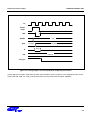
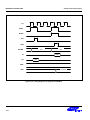
TIMING DIAGRAM
IRQ[i]
IRQ[i]
CK
nCLK_INT
nIACK
xx
IIR
i
BYTEH/
BYTEL
xx
SELREG
3h
nCLKIID
NOTE:
'xx' means unknown.
Figure 5-4. Timing Diagram for Interrupt Service
Figure 5-4 shows the timing diagram that any interrupt is generated and serviced. Only reading IIR clears the pending
bit. “nCLK_INT” will remain negative during any interrupt is remained to be serviced.
Figure 5-5 shows the interrupt by IMR. Initially the interrupt 1 is pending in IRQ[1] but not being serviced by masking
of IMR0. Writing ‘0000’ to IMR0 enables the pending interrupt 1 and requests the interrupt.
5-8
S3CC410 (Preliminary Spec)
INTERRUPT CONTROL UNIT
CK
BYTEH/
BYTEL
nWR
03h
SELREG
IMR0
DI
IRQ
16'h0001
16'h0000
16'h0
16'h0001
nCLK_INT
Figure 5-5. Timing Diagram for Interrupt Related to Masking Information
Timing diagram for register, especially byte-read and word-write is shown in figure 5-6. We suggests that the control
signal “nRD and “nWR” are a half-cycle signal because of timing hazard with the signal “SELREG”.
5-9
INTERRUPT CONTROL UNIT
S3CC410 (Preliminary Spec)
CK
BYTEL
BYTEH
nRD
nWR
01h
SELREG
DI
DO
02h
16'h0
8'h1
IMR0
IPR0
16'h01fd
16'h0000
Figure 5-6. Timing Diagram for Register Read/Write
5-10
S3CC410 (Preliminary Spec)
6
MEMORY MAP
MEMORY MAP
OVERVIEW
To support the control of peripheral hardware, the address for peripheral control registers are memory-mapped to the
area higher than 3F0000H. Memory mapping lets you use a mnemonic as the operand of an instruction in place of
the specific memory location.
In this section, detailed descriptions of the S3CC410 control registers are presented in an easy-to-read format.
You can use this section as a quick-reference source when writing application programs.
This memory area only can be accessed in privileged mode. If anyone tries to access this area in user mode, FIQ
(Fast Interrupt reQuest) occurs. And if you tries to access memory area higher than 3F018FH, FIQ occurs in
regardless of current operating mode. FIQ described here occurs only when the FE bit of the SR register is 1.
This control register is divided into six areas.
Control Register
3FFFFFH
Internal Program Memory
3F0190H
3F018FH
3F0150H
3F014FH
Violatation area (FIQ occurs if any
trial to access this region made)
LCD Control Register
External Memory Interface Register
ICACHE, DCACHE, MIU, DDMA, YDMA
3F0110H
3F010FH
Peripheral Control Register
3F0058H
3F0057H
Port Register Area
3F0030H
3F002FH
3F0008H
3F0007H
Timer16/ICU Area
System Control Register Area
3F0000H
Figure 6-1. Memory Mapped IO Registers
6-1
MEMORY MAP
S3CC410 (Preliminary Spec)
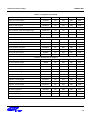
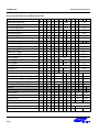
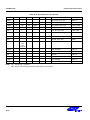
Table 6-1. Registers
Register Name
Mnemonic
Decimal
Hex
Reset
R/W
Location 00H are not mapped
Oscillator control register
Watch timer control register
OSCCON
1
01H
00H
R/W
WTCON
2
02H
00H
R/W
Location 03H are not mapped
Basic timer control register
BTCON
4
04H
00H
R/W
Basic timer counter
BTCNT
5
05H
00H
R
Watchdog timer enable register
WDTEN
6
06H
00H
R/W
Watchdog timer control register
WDTCON
7
07H
00H
R/W
Timer A control register
TACON
8
08H
00H
R/W
Timer A Pre-scalar register
TAPRE
9
09H
FFH
R/W
Timer A data register high
TADATAH
10
0AH
00H
R/W
Timer A data register low
TADATAL
11
0BH
00H
R/W
Timer A counter high
TACNTH
12
0CH
–
R
Timer A counter low
TACNTL
13
0DH
–
R
Location 1EH-1FH are not mapped
Timer B control register
TBCON
16
10H
00H
R/W
Timer B Pre-scalar register
TBPRE
17
11H
FFH
R/W
Timer B data register high
TBDATAH
18
12H
00H
R/W
Timer B data register low
TBDATAL
19
13H
00H
R/W
Timer B counter high
TBCNTH
20
14H
–
R
Timer B counter low
TBCNTL
21
15H
–
R
Location 16H-17H are not mapped
Timer C control register
TCCON
24
18H
00H
R/W
Timer C Pre-scalar register
TCPRE
25
19H
FFH
R/W
Timer C data register high
TCDATAH
26
1AH
00H
R/W
Timer C data register low
TCDATAL
27
1BH
00H
R/W
Timer C counter high
TCCNTH
28
1CH
–
R
Timer C counter low
TCCNTL
29
1DH
–
R
Location 1EH-1FH are not mapped
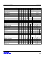
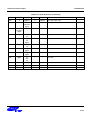
6-2
S3CC410 (Preliminary Spec)
MEMORY MAP
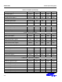
Table 6-1. Registers (Continued)
Register Name
Mnemonic
Decimal
Hex
Reset
R/W
Interrupt request register 0 high
IRQ0H
32
20H
–
R/W
Interrupt request register 0 low
IRQ0L
33
21H
–
R/W
Interrupt mask register 0 high
IMR0H
34
22H
00H
R/W
Interrupt mask register 0 low
IMR0L
35
23H
00H
R/W
Interrupt priority register 0 high
IPR0H
36
24H
00H
R/W
Interrupt priority register 0 low
IPR0L
37
25H
00H
R/W
Interrupt ID register 0 high
IIR0H
38
26H
–
R/W
Location 27H are not mapped
Interrupt request register 1 high
IRQ1H
40
28H
–
R/W
Interrupt request register 1 low
IRQ1L
41
29H
–
R/W
Interrupt mask register 1 high
IMR1H
42
2AH
00H
R/W
Interrupt mask register 1 low
IMR1L
43
2BH
00H
R/W
Interrupt priority register 1 high
IPR1H
44
2CH
00H
R/W
Interrupt priority register 1 low
IPR1L
45
2DH
00H
R/W
Location 2EH-2FH are not mapped
Port 0 data register
P0
48
30H
00H
R/W
Port 1 data register
P1
49
31H
00H
R/W
Port 2 data register
P2
50
32H
00H
R/W
Port 3 data register
P3
51
33H
00H
R/W
Port 4 data register
P4
52
34H
00H
R/W
Port 5 data register
P5
53
35H
00H
R
Port 6 data register
P6
54
36H
00H
R/W
Port 7 data register
P7
55
37H
00H
R/W
Port 8 data register
P8
56
38H
00H
R/W
Port 9 data register
P9
57
39H
00H
R/W
Port 10 data register
P10
58
3AH
00H
R/W
Location 3BH-3FH are not mapped
Port 0 control register
P0CON
64
40H
00H
R/W
Port 1 control register
P1CON
65
41H
00H
R/W
Port 2 control register high
P2CONH
66
42H
30H
R/W
Port 2 control register low
P2CONL
67
43H
00H
R/W
Port 3 control register high
P3CONH
68
44H
00H
R/W
Port 3 control register low
P3CONL
69
45H
00H
R/W
P3PUR
70
46H
00H
R/W
Port 3 pull-up resistor
Location 47H is not mapped
6-3
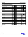
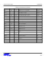
MEMORY MAP
S3CC410 (Preliminary Spec)
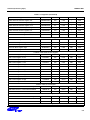
Table 6-1. Registers (Continued)
Register Name
Mnemonic
Decimal
Hex
Reset
R/W
Port 5 control register
P5CON
72
48H
00H
R/W
Port 5 pull-up resistor
P5PUR
73
49H
00H
R/W
Port 5 Int. Mode register High
P5INTMODH
74
4AH
00H
R/W
Port 5 Int. Mode register low
P5INTMODL
75
4BH
00H
R/W
P5INTCON
76
4CH
00H
R/W
Port 5 Int. control register
Location 4D-4FH are not mapped
Port 4 control register
P4CON
80
50H
00H
R/W
Port 4 Int. control register
P4INTCON
81
51H
00H
R/W
Port 4 Int. Mode register
P4INTMOD
82
52H
00H
R/W
Port 6 control register
P6CON
83
53H
00H
R/W
Port 7 control register
P7CON
84
54H
00H
R/W
Port 8 control register
P8CON
85
55H
00H
R/W
Port 9 control register
P9CON
86
56H
00H
R/W
Port 10 control register
P10CON
87
57H
00H
R/W
Smart Media control register
SMCON
88
58H
00H
R/W
ECC counter
ECCNT
89
59H
00H
R/W
ECC data register high
ECCH
90
5AH
00H
R/W
ECC data register low
ECCL
91
5BH
00H
R/W
ECC data register extension
ECCX
92
5CH
00H
R/W
ECCCLR
93
5DH
–
W
ECC result register high
ECCRSTH
94
5EH
00H
R/W
ECC result register low
ECCRSTL
95
5FH
00H
R/W
Parallel port data register
PPDATA
96
60H
00H
R/W
Parallel port command data register
PPCDATA
97
61H
00H
R/W
Parallel port status control register
PPSCON
98
62H
08H
R/W
Parallel port status register
PPSTAT
99
63H
3FH
R/W
Parallel port control register high
PPCONH
100
64H
00H
R/W
Parallel port control register low
PPCONL
101
65H
00H
R/W
Parallel port int. control register high
PPINTCONH
102
66H
00H
R/W
Parallel port int. control register low
PPINTCONL
103
67H
00H
R/W
Parallel port int. pending register high
PPINTPNDH
104
68H
00H
R/W
Parallel port int. pending register low
PPINTPNDL
105
69H
00H
R/W
Parallel port ack. width data register
PPACKD
106
6AH
xxH
R/W
ECC clear register
Location 6BH-6FH are not mapped
6-4
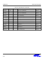
S3CC410 (Preliminary Spec)
MEMORY MAP
Table 6-1. Registers (Continued)
Register Name
Serial I/O control register
Serial I/O pre-scale register
Serial I/O data register
Mnemonic
Decimal
Hex
Reset
R/W
SIOCON
112
70H
00H
R/W
SIOPS
113
71H
00H
R/W
SIODATA
114
72H
00H
R/W
Location 73H are not mapped
A/D conversion result data register high
ADDATAH
116
74H
–
R
A/D conversion result data register low
ADDATAL
117
75H
–
R
ADCON
118
76H
00H
R/W
ADC control register
Location 77H-7FH are reserved for Future use
Function address register
FUNADDR
128
80H
00H
R
Power management register
PWRMAN
129
81H
00H
R
Frame number LO register
FRAMELO
130
82H
00H
R
Frame number HI register
FRAMEHI
131
83H
00H
R
Interrupt pending register
INTREG
132
84H
00H
R/W
Interrupt enable register
INTENA
133
85H
00H
R/W
Endpoint index register
EPINDEX
134
86H
00H
R/W
Locations 87H-88H are not mapped
Endpoint direction register
EPDIR
137
89H
00H
W
IN control status register
INCSR
138
8AH
00H
R/W
OUT control status register
OUTCSR
139
8BH
00H
R/W
IN MAX packet register
INMAXP
140
8CH
00H
R/W
OUT MAX packet register
OUTMAXP
141
8DH
00H
R/W
Write counter LO register
WRTCNTLO
142
8EH
00H
R/W
Write counter HI register
WRTCNTHI
143
8FH
00H
R/W
Endpoint 0 FIFO register
EP0FIFO
144
90H
00H
R/W
Endpoint 1 FIFO register
EP1FIFO
145
91H
00H
R/W
Endpoint 2 FIFO register
EP2FIFO
146
92H
00H
R/W
Endpoint 3 FIFO register
EP3FIFO
147
93H
00H
R/W
Location 94H – 9FH are invisible area for USB
IIS control register 0
IISCON0
160
A0H
00H
R/W
IIS mode register 0
IISMODE0
161
A1H
00H
R/W
IISPTR0
162
A2H
00H
R/W
IIS buffer pointer register 0
Location A3H is not mapped
6-5
MEMORY MAP
S3CC410 (Preliminary Spec)
Table 6-1. Registers (Continued)
Register Name
Mnemonic
Decimal
Hex
Reset
R/W
IIS control register 1
IISCON1
164
A4H
00H
R/W
IIS mode register 1
IISMODE1
165
A5H
00H
R/W
IISPTR1
166
A6H
00H
R/W
IIS buffer pointer register 1
Location A7H is not mapped
PLL0 data register higher
PLL0DATAH
168
A8H
–
R/W
PLL0 data register lower
PLL0DATAL
169
A9H
–
R/W
PLL0CON
170
AAH
0
R/W
PLL0 Control register
Location ABH is not mapped
PLL1 data register higher
PLL1DATAH
172
ACH
–
R/W
PLL1 data register lower
PLL1DATAL
173
ADH
–
R/W
PLL1CON
174
AEH
0
R/W
PLL1 Control register
Location AFH is not mapped
UART line control register
LCON
176
B0H
00H
R/W
UART control register
UCON
177
B1H
00H
R/W
UART status register
USSR
178
B2H
C0H
R
UART transmit buffer register
TBR
179
B3H
–
W
UART receive buffer register
RBR
180
B4H
–
R
UART baud rate divisor register
UBRDR
181
B5H
00H
R/W
UART interrupt pending register
UPEND
182
B6H
00
R/W
Location B7H is not mapped
IIC control register
IICCON
184
B8H
00H
R/W
IIC status register
IICSR
185
B9H
00H
R/W
IIC data register
IICDATA
186
BAH
–
R/W
IIC address register
IICADDR
187
BBH
–
R/W
IICPS
188
BCH
FFH
R/W
IICCNT
189
BDH
–
R
C0H FFH
–
R/W
IIC pre-scaler register
IIC pre-scaler count register for test
Location BEH – BFH are not mapped
64 Byte IIS I/O Buffer
BUF64
ID/Security register 0 higher
IDSC0H
256
100H
00H
R/W
ID/Security register 0 lower
IDSC0L
257
101H
–
R/W
ID/Security register 1 higher
IDSC1H
258
102H
–
R/W
ID/Security register 1 lower
IDSC1L
259
103H
–
R/W
ID/Security register 2 higher
IDSC2H
260
104H
–
R/W
ID/Security register 2 lower
IDSC2L
261
105H
–
R/W
ID/Security register 3 higher
IDSC3H
262
106H
–
R/W
6-6
S3CC410 (Preliminary Spec)
ID/Security register 3 lower
MEMORY MAP
IDSC3L
263
107H
–
R/W
6-7
MEMORY MAP
S3CC410 (Preliminary Spec)
Table 6-1. Registers (Continued)
Register Name
Mnemonic
Decimal
Hex
Reset
R/W
RANCON
264
108H
–
R/W
LFSR8
265
109H
–
R/W
16-bit linear feedback shift register higher
LFSR16H
266
10AH
–
R/W
16-bit linear feedback shift register lower
LFSR16L
267
10BH
–
R/W
Interrupt Service Mode register
INTMODE
268
10CH
00H
R/W
Control register for Random number generator
8-bit linear feedback shift register
Location 10D-10FH are not mapped
SRAM Configure register
MIUSCFG
272
110H
00H
R/W
SRAM Command register
MIUDCOM
273
111H
00H
R/W
SDRAM Configure register High
MIUDCFGH
274
112H
00H
R/W
SDRAM Configure register Low
MIUDCFGL
275
113H
00H
R/W
SDRAM Auto Refresh Count Value High
MIUDCNTH
276
114H
7H
R/W
SDRAM Auto Refresh Count Value Low
MIUDCNTL
277
115H
FFH
R/W
Location 116H – 11FHare not mapped
DDMA Command & Status register
DDMACOM
288
120H
00H
R/W
DDMA Configure register
DDMACFG
289
121H
00H
R/W
Location 122H are not mapped
DDMA Internal Address register eXt
DDMAIADRX
291
123H
–
R/W
DDMA Internal Address register High
DDMAIADRH
292
124H
–
R/W
DDMA Internal Address register Low
DDMAIADRL
293
125H
–
R/W
Location 126H are not mapped
DDMA External Address register eXt
DDMAEADRX
295
127H
–
R/W
DDMA External Address register High
DDMAEADRH
296
128H
–
R/W
DDMA External Address register Low
DDMAEADRL
297
129H
–
R/W
DDMA Transfer Number register High
DDMANUMH
298
12AH
–
R/W
DDMA Transfer Number register Low
DDMANUML
299
12BH
–
R/W
DDMA Transfer Count register High
DDMACNTH
300
12CH
00H
R
DDMA Transfer Count register Low
DDMACNTL
301
12DH
00H
R
DDMA Transfer Number register eXt
DDMANUMX
302
12EH
–
R/W
DDMA Transfer Count register eXt.
DDMACNTX
303
12FH
00H
R
YDMA Command & Status register
YDMACOM
304
130H
00H
R/W
YDMA Configure register
YDMACFG
305
131H
00H
R/W
YDMA Internal Address register High
YDMAIADRH
306
132H
–
R/W
YDMA Internal Address register Low
YDMAIADRH
307
133H
–
R/W
Location 134H are not mapped
6-8
S3CC410 (Preliminary Spec)
MEMORY MAP
Table 6-1. Registers (Continued)
Register Name
Mnemonic
Decimal
Hex
Reset
R/W
YDMA External Address register eXt
YDMAEADRX
309
135H
–
R/W
YDMA External Address register High
YDMAEADRH
310
136H
–
R/W
YDMA External Address register Low
YDMAEADRL
311
137H
–
R/W
YDMA Transfer Number register High
YDMANUMH
312
138H
–
R/W
YDMA Transfer Number register Low
YDMANUML
313
139H
–
R/W
YDMA Transfer Count register High
YDMACNTH
314
13AH
00H
R
YDMA Transfer Count register Low
YDMACNTL
315
13BH
00H
R
Location 13C-13FH are not mapped
CACHE Control register
CACHECON
320
140H
00H
R/W
ICACHE Base register High
ICBASEH
321
141H
00H
R/W
ICACHE Base register Low
ICBASEL
322
142H
00H
R/W
DCACHE Base register High
DCBASEH
323
143H
00H
R/W
DCACHE Base register Low
DCBASEL
324
144H
00H
R/W
Location 145H-14FH are not mapped
LCD Control register 0 High
LCNTR0H
336
150H
00H
R/W
LCD Control register 0 Low
LCNTR0L
337
151H
00H
R/W
LCD Control register 1 High
LCNTR1H
338
152H
00H
R/W
LCD Control register 1 Low
LCNTR1L
339
153H
00H
R/W
LCD Control register 2 High
LCNTR2H
340
154H
00H
R/W
LCD Control register 2 Low
LCNTR2L
341
155H
00H
R/W
LCD Control register 3 High
LCNTR3H
342
156H
00H
R/W
LCD Control register 3 Low
LCNTR3L
343
157H
00H
R/W
LCD Control register 4 High
LCNTR4H
344
158H
00H
R/W
LCD Control register 4 Low
LCNTR4L
345
159H
00H
R/W
LCD Control register 5 High
LCNTR5H
346
15AH
00H
R/W
LCD Control register 5 Low
LCNTR5L
347
15BH
00H
R/W
Location 15CH is not mapped
LCD DMA Channel 1 Base address High
LDBAR1H
349
15DH
00H
R/W
LCD DMA Channel 1 Base address Middle
LDBAR1M
350
15EH
00H
R/W
LCD DMA Channel 1 Base address Low
LDBAR1L
351
15FH
00H
R/W
Location 160H is not mapped
LCD DMA Channel 2 Base address High
LDBAR2H
353
161H
00H
R/W
LCD DMA Channel 2 Base address Middle
LDBAR2M
354
162H
00H
R/W
LCD DMA Channel 2 Base address Low
LDBAR2L
355
163H
00H
R/W
Location 164H is not mapped
6-9
MEMORY MAP
S3CC410 (Preliminary Spec)
Table 6-1. Registers (Continued)
Register Name
Mnemonic
Decimal
Hex
Reset
R/W
LCD DMA Channel 1 Current address High
LDCAR1H
349
165H
00H
R
LCD DMA Channel 1 Current address Middle
LDCAR1M
350
166H
00H
R
LCD DMA Channel 1 Current address Low
LDCAR1L
351
167H
00H
R
Location 168H is not mapped
LCD DMA Channel 2 Current address High
LDCAR2H
349
169H
00H
R
LCD DMA Channel 2 Current address Middle
LDCAR2M
350
16AH
00H
R
LCD DMA Channel 2 Current address Low
LDCAR2L
351
16BH
00H
R
Location 16CH is not mapped
LCD Status register
LSR
353
16DH
00H
R/W
LCD Red Lookup Table High-High
LRLUTRHH
354
16EH
00H
R/W
LCD Red Lookup Table High-Low
LRLUTRHL
355
16FH
00H
R/W
LCD Red Lookup Table Low-High
LRLUTRLH
356
170H
00H
R/W
LCD Red Lookup Table Low-Low
LRLUTRLL
357
171H
00H
R/W
LCD Green Lookup Table High-High
LGLUTRHH
358
172H
00H
R/W
LCD Green Lookup Table High-Low
LGLUTRHL
359
173H
00H
R/W
LCD Green Lookup Table Low-High
LGLUTRLH
360
174H
00H
R/W
LCD Green Lookup Table Low-Low
LGLUTRLL
361
175H
00H
R/W
LCD Blue Lookup Table Low-High
LBLUTRH
362
176H
00H
R/W
LCD Blue Lookup Table Low-Low
LBLUTRL
363
177H
00H
R/W
LCD 1/7 Dither Pattern register
LDP1_7
364
178H
00H
R/W
LCD 3/7 Dither Pattern register
LDP3_7
365
179H
00H
R/W
LCD 4/7 Dither Pattern register
LDP4_7
366
17AH
00H
R/W
LCD 5/7 Dither Pattern register
LDP5_7
367
17BH
00H
R/W
LCD 6/7 Dither Pattern register
LDP6_7
368
17CH
00H
R/W
Location 17DH is not mapped
LCD 1/5 Dither Pattern register
LDP1_5
370
17EH
00H
R/W
LCD 2/5 Dither Pattern register
LDP2_5
371
17FH
00H
R/W
LCD 3/5 Dither Pattern register
LDP3_5
372
180H
00H
R/W
LCD 4/5 Dither Pattern register
LDP4_5
373
181H
00H
R/W
LCD 1/4,1/2 Dither Pattern register
LDP1_4
374
182H
00H
R/W
LCD 3/4 Dither Pattern register
LDP3_4
375
183H
00H
R/W
LCD 1/3,2/3 Dither Pattern register
LDP1_3
376
184H
00H
R/W
Location 185H-18FH are not mapped
Location 190-FFFFH are not mapped
6-10
S3CC410 (Preliminary Spec)
MEMORY MAP
NOTES
6-11
S3CC410 (Preliminary Spec)
7
INSTRUCTION SET
INSTRUCTION SET
ALU INSTRUCTIONS
In operations between a 16-bit general register and an immediate value, the immediate value is zero-extended to 16bit. The following figure shows an example of 7-bit immediate numbers.
6
0
7-bits Immediate
imm: 7
15
7
'0'
7-bits Immediate
In operations between a 22-bit register and an immediate value, the immediate value is zero-extended to 22-bit. In
operations between a 22-bit register and a 16-bit register, the 16-bit register is zero-extended to 22-bit. The overflow
flag in a 16-bit arithmetic operation is saved to V flag in SR register. ALU instructions are classified into 3 classes as
follows.
•
ALUop Register, Immediate
•
ALUop Register, Register
•
ALUop Register
7-1
INSTRUCTION SET
S3CC410 (Preliminary Spec)
ALUOP REGISTER, IMMEDIATE
ADD/ADC/SUB/SBC/AND/OR/XOR/TST/CMP/CMPU Rn, #imm:16
The instructions perform an ALU operation of which source operands are a 16-bit general register Rn and a 16-bit
immediate value. In the instructions TST/CMP/CMPU, only T flag is updated accordingly as the result. In the
instructions ADD/ADC/SUB/SBC, the value of T flag is the carry flag of the operations, and the value of V flag
indicates whether overflow or underflow occurs. In the instructions AND/OR/XOR/TST, the value of T flag indicates
whether the result is zero (T=1). “CMP {GT|GE|EQ}, Rn, #imm:16” instructions are for signed comparison operations
(GT for greater than, GE for greater than or equal to and EQ for equal to), and “CMPU {GT|GE}, Rn, #imm:16”
instructions are for unsigned comparison operations.
NOTE:
imm:16 is defined as a 16-bit immediate number
ADD/SUB An, #imm:16
The immediate value is zero-extended to 22-bit value. No flag update occurs.
ADD/SUB Rn, #imm:7
The immediate value is zero-extended to 16-bit value. T flag is updated to the carry of the operation. V flag is
updated.
AND/OR/XOR/TST R0, #imm:8
The immediate value is zero-extended to 16-bit value. T flag indicates whether the lower 8-bit of the logical operation
result is zero.
CMP EQ, Rn, #imm:8
The immediate value is zero-extended to 16-bit value. Rn is restricted to R0 to R7. T flag is updated as the result of
the instruction.
CMP GE, Rn, #imm:6
The immediate value is zero-extended to 16-bit value. The instruction is for signed compare. T flag is updated as the
result of the instruction.
ADD/SUB An, #imm:5
The immediate value is zero-extended to 22-bit value. No flag is updated.
7-2
S3CC410 (Preliminary Spec)
INSTRUCTION SET
ALUOP REGISTER, REGISTER
ADD/SUB/ADC/SBC/AND/OR/XOR/TST/CMP/CMPU Rn, Ri
The instructions perform an ALU operation of which source operands are a pair of 16-bit general registers. In the
instructions TST/CMP/CMPU, only T flag is updated as the result. In the instructions ADD/ADC/SUB/SBC, the value
of T flag is the carry of the operations, and the value of V flag indicates whether overflow or underflow occurs. In the
instructions AND/OR/XOR/TST, the value of T flag indicates whether the result is zero. “CMP {GT|GE|EQ}, Rn, Ri”
instructions are for signed comparison, and “CMPU {GT|GE}, Rn, Ri” instructions are for unsigned comparison.
ADD/SUB An, Ri
16-bit general register Ri is zero-extended to 22-bit value. The result is saved in the 22-bit register An. No flag update
occurs.
CMP EQ, An, Ai
The instruction compares two 22-bit registers.
MUL {SS|SU|US|UU}, Rn, Ri
The general registers Rn and Ri can be one of R0 to R7. The instruction multiplies the lower byte of Rn and the
lower byte of Ri, and the 16-bit result is saved in Rn. The optional field, SS, SU, US, and UU, indicates whether the
source operands are signed value or unsigned value. The first letter of the two letter qualifiers corresponds to Rn, and
the second corresponds to Ri. For example, in the instruction “MUL SU, R0, R1”, the 8-bit signed value in the lower
byte of R0 and the 8-bit unsigned value in the lower byte of R1 are multiplied, and the 16-bit result is saved in R0.
RR/RL/RRC/SR/SRA/SLB/SRB/DT/INCC/DECC/COM/COM2/COMC/EXT Rn
For “DT Rn”(Decrement and Test) and “COM Rn”(Complement) instructions, T flag indicates whether the result is
zero. In the instruction of “EXT Rn”(Sign Extend), no flag update occurs. In all other instructions, carry-out of the
operation is transferred to T flag. In the instruction of DT, INCC, and DECC, V flag indicates whether overflow or
underflow occurs.
7-3
INSTRUCTION SET
S3CC410 (Preliminary Spec)
LOAD INSTRUCTIONS
“Load instructions” move data from register/memory/immediate to register/memory. When the destination is a
memory location, only general registers and extension registers can be the source. We can classify “Load
instructions” into the following 4 classes.
•
LD Register, Register
•
LD Register, Immediate
•
LD Data Memory, Register / LD Register, Data Memory
•
LD Register, Program Memory
LD REGISTER, REGISTER
LD Rn, Ri / LD An, Ai
The instructions move 16-bit or 22-bit data from the source register to the destination register. When the destination
register is R6/R7, the zero flag Z0/Z1 is updated. In all other cases, no flag update occurs.
LD Rn, Ei / LD En, Ri
In the instruction “LD Rn, Ei”, the 6-bit data in Ei is zero-extended to 16-bit data, and then transferred to Rn. When
the destination register is R6/R7, the zero flag Z0/Z1 is updated. In the instruction “LD En, Ri”, least significant 6 bits
of Ri are transferred to En. Rn/Ri is one of the registers from R0 to R7.
LD R0, SPR / LD SPR, R0
SPR : SR, SPCL_FIQ, SPCH_FIQ, SSR_FIQ, SPCL_IRQ, SPCH_IRQ, SSR_IRQ, SSR_SWI
The instructions transfer data between SPR (Special Purpose Registers) and R0. No flag update occurs except the
case that the destination register is SR.
LD An, PC
The instruction moves the value of (PC+4) to An.
7-4
S3CC410 (Preliminary Spec)
INSTRUCTION SET
LD REGISTER, DATA MEMORY / LD DATA MEMORY, REGISTER
LDW Rn, @[SP+edisp:9] / LDW @[SP+edisp:9], Rn
The instructions transfer 16-bit data between a general register Rn and the memory location at the address of
(SP+edisp:9). Note SP is another name of A15. edisp:9 is an even positive displacement from 0 to 510. edisp:9 is
encoded into an 8-bit displacement value in the instruction map because the LSB is always 0. When the address is
calculated, the 8-bit displacement field is shifted to the left by one bit, and then the result is added to the value of
SP. Even if the address might be specified as odd in assembly mnemonic, the LSB of the address should be
truncated to zero for word alignment.
LDW Rn, @[Ai+edisp:5] / LDW @[Ai+edisp:5], Rn
The instructions transfer 16-bit data between a general register Rn and the memory location at the address of
(Ai+edisp:5). edisp:5 is an even positive displacement from 0 to 30. edisp:5 is encoded into an 4-bit displacement
value in the instruction map because the LSB is always 0. When the address is calculated, the 4-bit displacement
field is shifted to the left by one bit, and then the result is added to the value of Ai. Even if the address might be
specified as odd in assembly mnemonic, the LSB of the address should be truncated to zero for word alignment.
LDW Rn, @[Ai+disp:16] / LDW @[Ai+disp:16], Rn
The instructions transfer 16-bit data between a general register Rn and the memory location at the address of
(Ai+disp:16). disp:16 is an positive displacement from 0 to FFFFh. If the address is odd, the LSB of the address is
set to zero for word alignment.
LDW Rn, @[Ai+Rj] / LDW @[Ai+Rj], Rn
The instructions transfer 16-bit data between a general register Rn and the memory location at the address of
(Ai+Rj). The value of Rj is zero-extended to 22-bit value. If the address is odd, the LSB of the address is set to zero
for word alignment.
LDW An, @[Ai+edisp:5] / LDW @[Ai+edisp:5], An
The instructions transfer 22-bit data between an address register An and the memory location at the address of
(Ai+edisp:5). edisp:5 is an even positive displacement from 0 to 30. edisp:5 is encoded into an 4-bit displacement
value in the instruction map because the LSB is always 0. When the address is calculated, the 4-bit displacement
field is shifted to the left by one bit, and then the result is added to the value of Ai. Even if the address might be
specified as odd in assembly mnemonic, the LSB of the address should be truncated to zero for word alignment.
LDW An, @[Ai+disp:16] / LDW @[Ai+disp:16], An
The instructions transfer 22-bit data between an address register An and the memory location at the address of
(Ai+disp:16). disp:16 is an positive displacement from 0 to FFFFh. If the address is odd, the LSB of the address is
set to zero for word alignment.
LDW An, @[Ai+Rj] / LDW @[Ai+Rj], An
The instructions transfer 22-bit data between an address register An and the memory location at the address of
(Ai+Rj). The value of Rj is zero-extended to 22-bit value. If the address is odd, the LSB of the address is set to zero
for word alignment.
7-5
INSTRUCTION SET
S3CC410 (Preliminary Spec)
PUSH Rn/PUSH Rn, Rm/PUSH An/ PUSH An, Am
The instruction “PUSH Rn” transfers 16-bit data from the register Rn to the memory location at the address of SP,
and then increments the value of SP by 2. The register Rn should not be R15. The operation of “PUSH R15” is
undefined. The instruction “PUSH Rn, Rm” pushes Rn and then Rm. The registers Rn and Rm should not be the
same. The registers Rn and Rm should not be R15. The instruction “PUSH An” pushes Rn and then En. When the
extension register En is pushed, the value of En is zero-extended to 16-bit data. The register An should not be A15.
The instruction “PUSH An, Am” pushes An and then Am. The registers An and Am should not be the same
POP Rn/POP Rn, Rm/POP An/ POP An, Am
The instruction “POP Rn” decrements the value of SP by 2, and then transfers 16-bit data to the register Rn from the
memory location at the address of SP. The register Rn should not be R15. The operation of “POP R15” is undefined.
The instruction “POP Rn, Rm” pops Rn and then Rm. The registers Rn and Rm should not be the same. The
registers Rn and Rm should not be R15. The instruction “POP An” pops En and then Rn. When the extension
register En is popped, the least significant 6 bits are transferred to En. The register An should not be A15. The
instruction “POP An, Am” pops An and then Am. The registers An and Am should not be the same
LDB Rn, @[Ai+disp:4] / LDB @[Ai+disp:4], Rn
The instructions transfer 8-bit data between the general register Rn and the memory location at the address of
(Ai+disp:4). disp:4 is a positive displacement from 0 to 15. The general register Rn is one R0 to R7. In the instruction
“LDB Rn, @[Ai+disp:4]”, the 8-bit data is zero-extended to 16-bit data, and then written into Rn. In the instruction
“LDB @[Ai+disp:8], Rn”, the least significant byte of Rn is transferred to the memory.
LDB Rn, @[Ai+disp:16] / LDB @[Ai+disp:16], Rn
The instructions transfer 8-bit data between the general register Rn and the memory location at the address of
(Ai+disp:16). disp:16 is a positive displacement from 0 to FFFFh. The general register Rn is one of R0 to R7. In the
instruction “LDB Rn, @[Ai+disp:16]”, the -bit data is zero-extended to 16-bit data, and then written into Rn. In the
instruction “LDB @[Ai+disp:16], Rn”, the least significant byte of Rn is transferred to the memory.
LDB R0, @[A8+disp:8] / LDB @[A8+disp:8], Rn
The instructions transfer 8-bit data between the general register R0 and the memory location at the address of
(A8+disp:8). disp:8 is a positive displacement from 0 to 255. In the instruction “LDB R0, @[A8+disp:8]”, the 8-bit
data is zero-extended to 16-bit data, and then written into R0. In the instruction “LDB @[A8+disp:8], R0”, the least
significant byte of R0 is transferred to the memory.
LDB Rn, @[Ai+Rj] / LDB @[Ai+Rj], Rn
The instructions transfer 8-bit data between the general register Rn and the memory location at the address of
(Ai+Rj). The value of Rj is zero-extended to 22-bit value. The general register Rn is one of the 8 registers from R0 to
R7. In the instruction “LDB Rn, @[Ai+Rj]”, the 8-bit data is zero-extended to 16-bit data, and then written into R0. In
the instruction “LDB @[Ai+Rj], Rn”, the least significant byte of Rn is transferred to the memory.
7-6
S3CC410 (Preliminary Spec)
INSTRUCTION SET
LD REGISTER, PROGRAM MEMORY
LDC Rn, @Ai
The instruction transfers 16-bit data to Rn from program memory at the address of Ai.
LD REGISTER, # IMMEDIATE
LD Rn, #imm:8 / LD Rn, #imm:16 / LD An, #imm:22
The instructions move an immediate data to a register. In the instruction “LD Rn, #imm:8”, the immediate value is
zero-extended to 16-bit value.
7-7
INSTRUCTION SET
S3CC410 (Preliminary Spec)
BRANCH INSTRUCTIONS
CalmRISC16 has 2 classes of branch instructions: with a delay slot and without a delay slot. If a delay slot is filled
with a useful instruction (or an instruction which is not NOP), then the performance degradation due to the control
dependency can be minimized. However, if the delay slot cannot be used, then it should be NOP instruction, which
can increase the program code size. In this case, the corresponding branch instruction without a delay slot can be
used to avoid using NOP.
Some instructions are not permitted to be in the delay slot. The prohibited instructions are as follows.
— All 2-word instructions
— All branch and jump instructions including SWI, RETD, RET_SWI, RET_IRQ, RET
— BREAK instructions
When a prohibited instruction is in the delay slot, the operation of CalmRISC16 is undefined or unpredictable.
BSRD eoffset:13
In the instruction, called branch subroutine with a delay slot, the value (PC + 4) is saved into A14 register, the
instruction in the delay slot is executed, and then the program sequence is moved to (PC + 2 + eoffset:13), where
PC is the address of the instruction “BSRD eoffset:13”. The immediate value eoffset:13 is sign-extended to 22-bit
and then added to (PC+2). In general, the 13-bit offset field appears as a label in assembly programs. If the
instruction in the delay slot reads the value of A14, the value (PC+4) is read. The even offset eoffset:13 is encoded to
12bit signed offset in instruction map by dropping the least significant bit.
BRA/BRAD/BRT/BRTD/BRF/BRFD eoffset:11
In the branch instructions, the target address is (PC + 2 + eoffset:11). The immediate value eoffset:11 is signextended to 22-bit and then added to (PC+2). The “D” in the mnemonic stands for a delay slot. In general, the 11-bit
offset field appears as a label in assembly programs. BRA and BRAD instructions always branch to the target
address. BRT and BRTD instructions branch to the target address if T flag is set. BRF and BRFD instructions
branch to the target address if T flag is cleared. BRAD/BRTD/BRFD instructions are delay slot branch instructions,
therefore the instruction in the delay slot is executed before the branch to the target address or the branch decision
is made. The even offset eoffset:11 is encoded to 10-bit signed offset in instruction map by dropping the least
significant bit.
BRA/BRAD EC:2, eoffset:8
In the branch instructions, the target address is (PC + 2 + eoffset:8). The immediate value eoffset:8 is sign-extended
to 22-bit and then added to (PC+2). The EC:2 field indicates one of the 4 external conditions from EC0 to EC3 (input
pin signals to CalmRISC16). When the external condition corresponding to EC:2 is set, the program branches to the
target address. BRAD has a delay slot. The even offset eoffset:8 is encoded to 7-bit signed offset in instruction map
by dropping the least significant bit.
7-8
S3CC410 (Preliminary Spec)
INSTRUCTION SET
BNZD R6/R7, eoffset:8
In the branch instruction, the target address is (PC + 2 + eoffset:8). The immediate value eoffset:8 is sign- extended
to 22-bit and then added to (PC+2). “BNZD R6, eoffset:8” instruction branches to the target address if Z0 flag is
cleared. “BNZD R7, eoffset:8” instruction branches if Z1 flag is cleared. Before the branch operation, the instruction
decrements R6/R7, updates Z0/Z1 flag according to the decrement result, and then executes the instruction in the
delay slot. The instruction is used to manage loop counter with just one cycle overhead. In the end of the loop, the
value of R6/R7 is –1. When the instruction in the delay slot read the Z0/Z1 flag, the result after the decrement is
read. The even offset eoffset:8 is encoded to 7-bit signed offset in instruction map by dropping the least significant
bit.
JMP/JPT/JPF/JSR addr:22
The target address of the instructions is addr:22. JMP always branches to the target address. JPT branches to the
target address if the T flag is set. JPF branches if the T flag is cleared. JSR always branches to the target address
with saving the return address (PC+4) into A14. The instructions are 2 word instructions.
JMP/JPT/JPF/JSR Ai
The target address of the instructions is the value of Ai. JMP always branches to the target address. JPT branches
to the target address if the T flag is set. JPF branches if the T flag is cleared. JSR always branches to the target
address with saving the return address (PC+2) into A14.
SWI #imm:6/ RET_SWI/RET_IRQ/RET_FIQ
refer to the section for interrupts.
RETD
The instruction branches to the address in A14 after the execution of the instruction in the delay slot. When there is
no useful instruction adequate to the delay slot, “JMP A14” can be used instead of “RETD”.
7-9
INSTRUCTION SET
S3CC410 (Preliminary Spec)
BIT OPERATION
The bit operations manipulate a bit in SR register or in a memory location.
BITR/BITS/BITC/BITT @[A8+R1], #imm:3
The source as well as the destination is the 8-bit data in the data memory at the address (A8 + R1). The #imm:3
field chooses a bit position among the 8 bits. BITR resets the bit #imm:3 of the source, and then writes the result to
the destination, the same memory location. BITS sets the bit #imm:3 of the source, and then writes the result to the
destination. BITC complements the bit #imm:3 of the source, and then writes the result to the destination. BITT does
not write any data to the destination. T flag indicates whether the bit #imm:3 of the source is zero. In other words,
when the bit #imm:3 of the source is zero, T flag is set. BITR and BITS can be used to implement a semaphore
mechanism or lock acquisition/release.
CLRSR/SETSR/TSTSR bit
bit : FE, IE, TE, Z0, Z1, V, PM
CLRSR instruction clears the corresponding bit of SR. SETSR instruction sets the corresponding bit of SR. TSTSR
tests whether the corresponding bit is zero, and stores the result in T flag. For example, when IE flag is zero,
“TSTSR IE” instruction sets the T flag. We can clear the T flag by the instruction “CMP GT, R0, R0”. We can set the
T flag by the instruction “CMP EQ, R0, R0”.
7-10
S3CC410 (Preliminary Spec)
INSTRUCTION SET
MISCELLANEOUS INSTRUCTIONS
SYS #imm:5
The instruction activates the output port nSYSID. The #imm:5 is transferred to outside on DA[4:0]. The most
significant 17 bits remain unchanged. The instruction is for system command to outside such as power down
modes.
COP #imm:13
The instruction activates the output port nCOPID. The #imm:13 is transferred to outside on COPIR[12:0]. The
instruction is used to transfer instruction to coprocessor. The #imm:13 may be from 200h to 1FFFh.
CLD Rn, #imm:5 / CLD #imm:5, Rn
The instruction activates the output port nCOPID, nCLDID, and CLDWR. The least significant 13 bits of the
instruction is transferred to outside on COPIR[12:0]. The #imm:5 is transferred to outside on DA[4:0]. The
instructions move 16-bit data between Rn and a coprocessor register implied by the #imm:5 field. CLDWR signal
indicates whether the data movement is from CalmRISC16 to coprocessor. The register Rn is one 8 registers from
R0 to R7.
NOP
No operation.
BREAK
The software break instruction activates nBRK signal, and holds PA for one cycle. It’s for debugging operation.
7-11
INSTRUCTION SET
S3CC410 (Preliminary Spec)
CALMRISC16 INSTRUCTION SET MAP
Table 7-1. CalmRISC16 Instruction Set Map
15
8 7
0
ADD Rn, #imm:7
0
0
0
0
Rn
0
Imm:7
SUB Rn, #imm:7
0
0
0
0
Rn
1
Imm:7
LD Rn, #imm:8
0
0
0
1
Rn
Imm:8
LDW Rn, @[SP + edisp:9]
0
0
1
0
Rn
Edisp:9
LDW @[SP + edisp:9], Ri
0
0
1
1
Ri
Edisp:9
LDW Rn, @[Ai + edisp:5]
0
1
0
0
Rn
0
Ai
Edisp:5
LDW Rn, @[Ai + Rj]
0
1
0
0
Rn
1
Ai
Rj
LDW @[An + edisp:5], Ri
0
1
0
1
Ri
0
An
Edisp:5
LDW @[An + Rm], Ri
0
1
0
1
Ri
1
An
Rm
LDB Dn, @[Ai + disp:4]
0
1
1
0
0
Dn
0
Ai
Disp:4
LDB Dn, @[Ai + Rj]
0
1
1
0
0
Dn
1
Ai
Rj
LDW An, @[Ai + disp:4]
0
1
1
0
1
An
0
Ai
Disp:4
LDW An, @[Ai + Rj]
0
1
1
0
1
An
1
Ai
Rj
LDB @[An + disp:4], Di
0
1
1
1
0
Di
0
An
Disp:4
LDB @[An + Rm], Di
0
1
1
1
0
Di
1
An
Rm
LDW @[An + disp:4], Ai
0
1
1
1
1
Ai
0
An
Disp:4
LDW @[An + Rm], Ai
0
1
1
1
1
Ai
1
An
Rm
ADD Rn, Ri
1
0
0
0
Rn
0
0
0
0
Ri
SUB Rn, Ri
1
0
0
0
Rn
0
0
0
1
Ri
ADC Rn, Ri
1
0
0
0
Rn
0
0
1
0
Ri
SBC Rn, Ri
1
0
0
0
Rn
0
0
1
1
Ri
AND Rn, Ri
1
0
0
0
Rn
0
1
0
0
Ri
OR Rn, Ri
1
0
0
0
Rn
0
1
0
1
Ri
XOR Rn, Ri
1
0
0
0
Rn
0
1
1
0
Ri
TST Rn, Ri
1
0
0
0
Rn
0
1
1
1
Ri
CMP GE, Rn, Ri
1
0
0
0
Rn
1
0
0
0
Ri
CMP GT, Rn, Ri
1
0
0
0
Rn
1
0
0
1
Ri
CMPU GE, Rn, Ri
1
0
0
0
Rn
1
0
1
0
Ri
CMPU GT, Rn, Ri
1
0
0
0
Rn
1
0
1
1
Ri
CMP EQ, Rn, Ri
1
0
0
0
Rn
1
1
0
0
Ri
LD Rn, Ri
1
0
0
0
Rn
1
1
0
1
Ri
RR Rn
1
0
0
0
0
0
0
0
1
1
1
0
Rn
RL Rn
1
0
0
0
0
0
0
1
1
1
1
0
Rn
7-12
S3CC410 (Preliminary Spec)
INSTRUCTION SET
Table 7-1. CalmRISC16 Instruction Set Map (Continued)
15
8 7
0
RRC Rn
1
0
0
0
0
0
1
0
1
1
1
0
Rn
SRB Rn
1
0
0
0
0
0
1
1
1
1
1
0
Rn
SR Rn
1
0
0
0
0
1
0
0
1
1
1
0
Rn
SRA Rn
1
0
0
0
0
1
0
1
1
1
1
0
Rn
JPF Ai
1
0
0
0
0
1
1
0
1
1
1
0
0
Ai
JPT Ai
1
0
0
0
0
1
1
0
1
1
1
0
1
Ai
JMP Ai
1
0
0
0
0
1
1
1
1
1
1
0
0
Ai
JSR Ai
1
0
0
0
0
1
1
1
1
1
1
0
1
Ai
SLB Rn
1
0
0
0
1
0
0
0
1
1
1
0
Rn
DT Rn
1
0
0
0
1
0
0
1
1
1
1
0
Rn
INCC Rn
1
0
0
0
1
0
1
0
1
1
1
0
Rn
DECC Rn
1
0
0
0
1
0
1
1
1
1
1
0
Rn
COM Rn
1
0
0
0
1
1
0
0
1
1
1
0
Rn
COM2 Rn
1
0
0
0
1
1
0
1
1
1
1
0
Rn
COMC Rn
1
0
0
0
1
1
1
0
1
1
1
0
Rn
EXT Rn
1
0
0
0
1
1
1
1
1
1
1
0
Rn
ADD Rn, #imm:16
1
0
0
0
0
0
0
0
1
1
1
1
Rn
ADD An, #imm:16
1
0
0
0
0
0
0
1
1
1
1
1
0
An
SUB An, #imm:16
1
0
0
0
0
0
0
1
1
1
1
1
1
An
ADC Rn, #imm:16
1
0
0
0
0
0
1
0
1
1
1
1
Rn
SBC Rn, #imm:16
1
0
0
0
0
0
1
1
1
1
1
1
Rn
AND Rn, #imm:16
1
0
0
0
0
1
0
0
1
1
1
1
Rn
OR Rn, #imm:16
1
0
0
0
0
1
0
1
1
1
1
1
Rn
XOR Rn, #imm:16
1
0
0
0
0
1
1
0
1
1
1
1
Rn
TST Rn, #imm:16
1
0
0
0
0
1
1
1
1
1
1
1
Rn
CMP GE, Rn, #imm:16
1
0
0
0
1
0
0
0
1
1
1
1
Rn
CMP GT, Rn, #imm:16
1
0
0
0
1
0
0
1
1
1
1
1
Rn
CMPU GE, Rn, #imm:16
1
0
0
0
1
0
1
0
1
1
1
1
Rn
CMPU GT, Rn, #imm:16
1
0
0
0
1
0
1
1
1
1
1
1
Rn
CMP EQ, Rn, #imm:16
1
0
0
0
1
1
0
0
1
1
1
1
Rn
LD Rn, #imm:16
1
0
0
0
1
1
0
1
1
1
1
1
Rn
Reserved
1
0
0
0
1
1
1
1
1
1
1
CMP EQ, Dn, #imm:8
1
0
0
1
0
AND R0, #imm:8
1
0
0
1
1
Dn
0
0
Imm:8
0
Imm:8
7-13
INSTRUCTION SET
S3CC410 (Preliminary Spec)
Table 7-1. CalmRISC16 Instruction Set Map (Continued)
15
8 7
0
OR R0, #imm:8
1
0
0
1
1
0
0
1
Imm:8
XOR R0, #imm:8
1
0
0
1
1
0
1
0
Imm:8
TST R0, #imm:8
1
0
0
1
1
0
1
1
Imm:8
LDB R0, @[A8+ disp:8]
1
0
0
1
1
1
0
0
Disp:8
LDB @[A8+ disp:8],R0
1
0
0
1
1
1
0
1
Disp:8
BITR @[A8+R1], bs:3
1
0
0
1
1
1
1
0
0
0
0
0
0
Bs:3
BITS @[A8+R1], bs:3
1
0
0
1
1
1
1
0
0
0
0
0
1
Bs:3
BITC @[A8+R1], bs:3
1
0
0
1
1
1
1
0
0
0
0
1
0
Bs:3
BITT @[A8+R1], bs:3
1
0
0
1
1
1
1
0
0
0
0
1
1
Bs:3
SYS #imm:5
1
0
0
1
1
1
1
0
0
0
1
SWI #imm:6
1
0
0
1
1
1
1
0
0
1
CLRSR bs:3
1
0
0
1
1
1
1
0
1
0
0
0
0
Bs:3
SETSR bs:3
1
0
0
1
1
1
1
0
1
0
0
0
1
Bs:3
TSTSR bs:3
1
0
0
1
1
1
1
0
1
0
0
1
0
Bs:3
NOP
1
0
0
1
1
1
1
0
1
0
0
1
1
0
0
0
BREAK
1
0
0
1
1
1
1
0
1
0
0
1
1
0
0
1
LD R0, SR
1
0
0
1
1
1
1
0
1
0
0
1
1
0
1
0
LD SR, R0
1
0
0
1
1
1
1
0
1
0
0
1
1
0
1
1
RET_FIQ
1
0
0
1
1
1
1
0
1
0
0
1
1
1
0
0
RET_IRQ
1
0
0
1
1
1
1
0
1
0
0
1
1
1
0
1
RET_SWI
1
0
0
1
1
1
1
0
1
0
0
1
1
1
1
0
RETD
1
0
0
1
1
1
1
0
1
0
0
1
1
1
1
1
LD R0, SPCL_FIQ
1
0
0
1
1
1
1
0
1
0
1
0
0
0
0
0
LD R0, SPCH_FIQ
1
0
0
1
1
1
1
0
1
0
1
0
0
0
0
1
LD R0, SSR_FIQ
1
0
0
1
1
1
1
0
1
0
1
0
0
0
1
0
Reserved
1
0
0
1
1
1
1
0
1
0
1
0
0
0
1
1
LD R0, SPCL_IRQ
1
0
0
1
1
1
1
0
1
0
1
0
0
1
0
0
LD R0, SPCH_IRQ
1
0
0
1
1
1
1
0
1
0
1
0
0
1
0
1
LD R0, SSR_IRQ
1
0
0
1
1
1
1
0
1
0
1
0
0
1
1
0
Reserved
1
0
0
1
1
1
1
0
1
0
1
0
0
1
1
1
Reserved
1
0
0
1
1
1
1
0
1
0
1
0
1
0
0
LD R0, SSR_SWI
1
0
0
1
1
1
1
0
1
0
1
0
1
0
1
0
Reserved
1
0
0
1
1
1
1
0
1
0
1
0
1
0
1
1
Reserved
1
0
0
1
1
1
1
0
1
0
1
0
1
1
7-14
Imm:5
Imm:6
S3CC410 (Preliminary Spec)
INSTRUCTION SET
Table 7-1. CalmRISC16 Instruction Set Map (Continued)
15
8 7
0
LD SPCL_FIQ, R0
1
0
0
1
1
1
1
0
1
0
1
1
0
0
0
0
LD SPCH_FIQ, R0
1
0
0
1
1
1
1
0
1
0
1
1
0
0
0
1
LD SSR_FIQ, R0
1
0
0
1
1
1
1
0
1
0
1
1
0
0
1
0
Reserved
1
0
0
1
1
1
1
0
1
0
1
1
0
0
1
1
LD SPCL_IRQ, R0
1
0
0
1
1
1
1
0
1
0
1
1
0
1
0
0
LD SPCH_IRQ, R0
1
0
0
1
1
1
1
0
1
0
1
1
0
1
0
1
LD SSR_IRQ, R0
1
0
0
1
1
1
1
0
1
0
1
1
0
1
1
0
Reserved
1
0
0
1
1
1
1
0
1
0
1
1
0
1
1
1
Reserved
1
0
0
1
1
1
1
0
1
0
1
1
1
0
0
LD SSR_SWI, R0
1
0
0
1
1
1
1
0
1
0
1
1
1
0
1
0
Reserved
1
0
0
1
1
1
1
0
1
0
1
1
1
0
1
1
Reserved
1
0
0
1
1
1
1
0
1
0
1
1
1
1
Reserved
1
0
0
1
1
1
1
0
1
1
0
Reserved
1
0
0
1
1
1
1
0
1
1
1
0
LD An, PC
1
0
0
1
1
1
1
0
1
1
1
1
0
Reserved
1
0
0
1
1
1
1
0
1
1
1
1
1
JPF adr:22
1
0
0
1
1
1
1
1
0
0
Adr[21:16]
JPT adr:22
1
0
0
1
1
1
1
1
0
1
Adr[21:16]
JMP adr:22
1
0
0
1
1
1
1
1
1
0
Adr[21:16]
JSR adr:22
1
0
0
1
1
1
1
1
1
1
Adr[21:16]
LDC Rn, @Ai
1
0
1
0
0
0
0
0
0
Reserved
1
0
1
0
0
0
0
0
1
LD Dn, Ei
1
0
1
0
0
Dn
0
0
0
1
0
Ei
LD En, Di
1
0
1
0
0
Di
0
0
0
1
1
En
CMP EQ, An, Ai
1
0
1
0
1
An
0
0
0
1
0
Ai
LD An, Ai
1
0
1
0
1
An
0
0
0
1
1
Ai
LDW Rn, @[Ai+disp:16]
1
0
1
0
Rn
0
0
1
0
0
Ai
LDW @[An+disp:16], Ri
1
0
1
0
Ri
0
0
1
0
1
An
LDB Dn, @[Ai+disp:16]
1
0
1
0
0
Dn
0
0
1
1
0
Ai
LDB @[An+disp:16], Di
1
0
1
0
0
Di
0
0
1
1
1
An
LDW An, @[Ai+disp:16]
1
0
1
0
1
An
0
0
1
1
0
Ai
LDW @[An+disp:16], Ai
1
0
1
0
1
Ai
0
0
1
1
1
An
CMP GE, Dn, #imm:6
1
0
1
0
0
Dn
0
1
ADD An, #imm:5
1
0
1
0
1
An
0
1
0
imm:5
SUB An, #imm:5
1
0
1
0
1
An
0
1
1
imm:5
Rn
An
Ai
Imm:6
7-15
INSTRUCTION SET
S3CC410 (Preliminary Spec)
Table 7-1. CalmRISC16 Instruction Set Map (Continued)
15
8 7
0
CMP EQ, An, #imm:22
1
0
1
0
0
An
1
0
Imm[21:16]
LD An, #imm:22
1
0
1
0
1
An
1
0
Imm[21:16]
ADD An, Ri
1
0
1
0
0
An
1
1
0
0
Ri
SUB An, Ri
1
0
1
0
1
An
1
1
0
0
Ri
MUL UU, Dn, Di
1
0
1
0
0
Dn
1
1
0
1
0
Di
MUL US, Dn, Di
1
0
1
0
0
Dn
1
1
0
1
1
Di
MUL SU, Dn, Di
1
0
1
0
1
Dn
1
1
0
1
0
Di
MUL SS, Dn, Di
1
0
1
0
1
Dn
1
1
0
1
1
Di
POP Rn[, Rm]
1
0
1
0
1
1
1
0
0
Rn
Reserved
1
0
1
0
0
1
1
1
0
1
POP An[, Am]
1
0
1
0
1
1
1
1
0
1
An
PUSH Rn[, Rm]
1
0
1
0
1
1
1
1
0
Rn
Reserved
1
0
1
0
0
1
1
1
1
1
PUSH An[, Am]
1
0
1
0
1
1
1
1
1
1
BSRD eoffset:13
1
0
1
1
BRA EC:2, eoffset:8
1
1
0
0
0
0
0
Reserved
1
1
0
0
0
0
1
BRAD EC:2, eoffset:8
1
1
0
0
0
1
BNZD H, eoffset:8
1
1
0
0
0
Reserved
1
1
0
0
BRA eoffset:11
1
1
0
BRAD eoffset:11
1
1
BRF eoffset:11
1
BRFD eoffset:11
Rm
Am
Rm
Am
An
Eoffset:13
EC:2
Eoffset:8
0
EC:2
Eoffset:8
1
1
H
Eoffset:8
0
1
1
0
1
0
Eoffset:11
0
0
1
1
Eoffset:11
1
0
1
0
0
Eoffset:11
1
1
0
1
0
1
Eoffset:11
BRT eoffset:11
1
1
0
1
1
0
Eoffset:11
BRTD eoffset:11
1
1
0
1
1
1
Eoffset:11
CLD Dn, imm:5
1
1
1
0
0
0
0
imm:5
0
Dn
CLD imm:5, Di
1
1
1
0
0
0
0
imm:5
1
Di
COP imm:13
1
1
1
0
1
Imm:13
•
Dn[15:0] : R0-R7
•
EC:2 : EC0,EC1,EC2,EC3
•
H[15:0] : R6, R7
•
Disp : unsigned displacement
•
An[21:0] : A8-A15, concatenation of En and Rn
•
Eoffset : even signed offset
•
En[5:0] : E8-E15, MS 6-bit of An
•
Edisp : even unsigned displacement
•
SP : equal to A15
7-16
S3CC410 (Preliminary Spec)
INSTRUCTION SET
QUICK REFERENCE
Table 7-2. Quick Reference
Instruction
op1
op2
operation
ADD
SUB
Rn
#imm:7
Ri
LD
Rn
#imm:8
#imm:16
Ri
op1 <- op2
Z0, Z1
LDW
Rn
@[SP+edisp:9]
@[Ai+edisp:5]
@[Ai+Rj]
@[Ai+disp:16]
op1 <- op2
–
LDW
@[SP+edisp:9]
@[An+edisp:5]
@[An+Rm]
@[Ai+disp:16]
Ri
op1 <- op2
–
LDW
An
@[Ai+edisp:5]
@[Ai+Rj]
@[Ai+disp:16]
op1 <- op2
–
LDW
@[An+edisp:5]
@[An+Rm]
@[Ai+disp:16]
Ai
op1 <- op2
–
LDB
Dn
@[SP+disp:8]
@[Ai+disp:4]
@[Ai+Rj]
@[Ai+disp:16]
op1<-{8’h0,op2[7:0]}
–
LDB
R0
@[A8+disp:8]
op1<-{8’h0,op2[7:0]}
–
LDB
@[SP+disp:8]
@[An+disp:4]
@[Ai+Rj]
@[Ai+disp:16]
Di
op1 <- op2[7:0]
–
LDB
@[A8+disp:8]
R0
op1 <- op2[7:0]
–
ADC
SBC
Rn
Ri
#imm:16
op1 <- op1 + op2 + T
op1 <- op1 + ~op2 + T
AND
OR
XOR
Rn
Ri
#imm:16
op1 <- op1 & op2
op1 <- op1 | op2
op1 <- op1 ^ op2
TST
Rn
Ri
#imm:16
op1 & op2
op1 <- op1 + op2
op1 <- op1 + ~op2 + 1
flag
T=C, Z0, Z1,V
T=C,V,
Z0,Z1
T=Z,
Z0,Z1
T=Z
7-17
INSTRUCTION SET
S3CC410 (Preliminary Spec)
Table 7-2. Quick Reference (Continued)
Instruction
op1
op2
CMP GE
CMP GT
CMPU GE
CMPU GT
CMP EQ
Rn
Ri
RR
RL
RRC
SRB
SR
SRA
SLB
Rn
DT
Rn
#imm:16
–
operation
flag
op1 + ~op2 + 1, T=~N
op1 + ~op2 + 1, T=~N&~Z
op1 + ~op2 + 1, T=C
op1 + ~op2 + 1, T=C&~Z
op1 + ~op2 + 1, T=Z
T
op1 <- {op1[0],op1[15:1]}
op1 <- {op1[14:0],op1[15]}
op1 <- {T,op1[15:1]}
op1 <- {8’h00,op1[15:8]}
op1 <- {0,op1[15:1]}
op1 <- {op1[15],op1[15:1]}
op1 <- {op1[7:0],8’h00}
T=op1[0]
T=op1[15]
T=op1[0]
T=op1[7]
T=op1[0]
T=op1[0]
T= op1[8]
op1 <- op1 + 0xffff
T=Z,
Z0,Z1,V
COM
Rn
op1 <- ~op1
T=Z,Z0,
Z1
INCC
DECC
COM2
COMC
Rn
op1 <- op1 + T
op1 <- op1 + 0xffff + T
op1 <- ~op1 + 1
op1 <- ~op1 + T
EXT
Rn
op1<-{8{op1[7]},op1[7:0]}
JPF
JPT
JMP
JSR
Ai
addr:22
if(T==0) PC <- op1
if(T==1) PC <- op1
PC <- op1
A14 <- PC+(2|4), PC<-op1
ADD
Rn
#imm:16
op1 <- op1 + op2
T=C,Z0,
Z1
Z0, Z1
–
T=C,
Z0,Z1,V
ADD
SUB
An
#imm:16
#imm:5
op1 <- op1 + op2
op1 <- op1 – op2
–
Ri
CMP EQ
Dn
#imm:8
op1 + ~op2 + 1
T=Z
AND
OR
XOR
TST
R0
#imm:8
op1 <- op1 & {8’h00,op2}
op1 <- op1 | {8’h00,op2}
op1 <- op1 ^ {8’h00,op2}
op1 & {8’h00,op2}
T=Z8
BITR
BITS
BITC
BITT
@[A8+R1]
bs:3
SYS
#imm:5
–
DA[4:0] <- op1
SWI
#imm:6
–
A14 <- PC+2, PC <- op2*4
7-18
op1[op2] <- 0
op1[op2] <- 1
op1[op2] <- ~op1[op2]
op1[op2] <- op1[op2]
T= op1[op2]
–
IE, TE
S3CC410 (Preliminary Spec)
INSTRUCTION SET
Table 7-2. Quick Reference (Continued)
Instruction
op1
op2
bs:3
–
SR[op1] <- 0
SR[op1] <- 1
T <- ~SR[op1]
–
–
–
PC <- A14
–
LD
R0
SR
SPCL_FIQ
SPCH_FIQ
SSR_FIQ
SPCL_IRQ
SPCH_IRQ
SSR_IRQ
SSR_SWI
op1 <- op2
–
LD
SR
SPCL_FIQ
SPCH_FIQ
SSR_FIQ
SPCL_IRQ
SPCH_IRQ
SSR_IRQ
SSR_SWI
R0
op1 <- op2
LD
An
PC
Ai
#imm:22
op1 <- op2 + 4
CLRSR
SETSR
TSTSR
RETD
operation
flag
–
op1 <- op2
op1 <- op2
CMP EQ
An
Ai
#imm:22
op1 + ~op2 + 1
T=Z22
LDC
Rn
@Ai
op1 <- PM[op2]
–
LD
Rn
Ei
op1 <- {10’h000, op2}
–
LD
En
Ri
op1 <- op2[5:0]
–
CMP GE
Dn
#imm:6
op1 + ~op2 + 1
T=~N
MUL
MUL
MUL
MUL
Dn
Di
POP
Rn
PUSH
Rn
UU
US
SU
SS
op1<-{0,op1[7:0]} * {0,op2[7:0]}
op1<-{0,op1[7:0]}*{op2[7],op2[7:0]}
op1<-{op1[7],op1[7:0]}*{0,op2[7:0]}
op1 <-{op1[7],op1[7:0]}*
{op2[7],op2[7:0]}
–
Rm
op1<-@[SP+2], op2<-@[SP+4],
SP<-SP+4
–
Rm
@[SP]<-op1,@[SP-2]<-op2,SP<-SP-4
–
7-19
INSTRUCTION SET
S3CC410 (Preliminary Spec)
Table 7-2. Quick Reference (Continued)
Instruction
op1
op2
POP
An
Am
En<-@[SP+2], Rn<-@[SP+4], Em<@[SP+6], Rm<-@[SP+8], SP<-SP+8
–
PUSH
An
Am
@[SP]<-Rn, @[SP-2]<-En, @[SP-4]<Rm, @[SP-6]<-Em, SP<-SP-8
–
BSRD
eoffset:13
–
A14 <- PC+2, PC <- PC + 2 + op1
–
EC:2
eoffset:8
if(EC:2 == 1) PC <- PC + 2 + op2
–
BNZD
R6
eoffset:8
if(Z0 == 0) PC <- PC + 2 + op2
R6 <- R6 – 1
Z0
BNZD
R7
eoffset:8
if(Z1 == 0) PC <- PC + 2 + op2
R7 <- R7 – 1
Z1
BRA/BRAD
eoffset:11
–
PC <- PC + 2 + op1
–
BRF/BRFD
eoffset:11
–
if(T==0) PC <- PC + 2 + op1
–
BRT/BRTD
eoffset:11
–
if(T==1) PC <- PC + 2+op1
–
CLD
Dn
imm:5
op1 <- Coprocessor[op2]
–
CLD
imm:5
Di
Coprocessor[op1] <- op2
COP
imm:13
–
COPIR <- op2
BRA/BRAD
7-20
operation
flag
S3CC410 (Preliminary Spec)
INSTRUCTION SET
ADC (1) – Add with Carry Register
Format:
ADC Rn, Ri
Description:
The ADC (Add with Carry Register) instruction is used to synthesize 32-bit addition. If register pairs
R0, R1 and R2, R3 hold 32-bit values (R0 and R2 hold the least-significant word), the following
instructions leave the 32-bit sum in R0, R1:
ADD R0, R2
ADC R1, R3
The instruction ADC R0, R0 produces a single-bit Rotate Left with Carry (17-bit rotate through the
carry) on R0.
ADC adds the value of register Rn, and the value of the Carry flag (stored in the T bit), and the value
of register Ri, and stores the result in register Rn. The T bit and the V flag are updated based on the
result.
7-21
INSTRUCTION SET
S3CC410 (Preliminary Spec)
ADC (2) – Add with Carry Immediate
Format:
ADC Rn, #<imm:16>
Description:
The ADC (Add with Carry Immediate) instruction is used to synthesize 32-bit addition with an
immediate operand. If register pair R0, R1 holds a 32-bit value (R0 holds the least-significant word),
the following instructions leave the 32-bit sum with 87653456h in R0, R1:
ADD R0, #3456h
ADC R1, #8765h
ADC adds the value of register Rn, and the value of the Carry flag (stored in the T bit), and the 16-bit
immediate operand, and stores the result in register Rd. The T bit and the V flag are updated based
on the result.
Operation:
15
14
13
12
11
10
9
8
7
6
5
4
1
0
0
0
0
0
1
0
1
1
1
1
3
0
Rn
Rn := Rn + <imm:16> + T bit
T bit := Carry from (Rn + <imm:16> + T bit)
V flag := Overflow from (Rn + <imm:16> + T bit)
if(Rn == R6/R7) Z0/Z1 flag := ((Rn + <imm:16>) == 0)
Exceptions:
None.
Notes:
This is a 2-word instruction, where the 16-bit immediate follows the instruction word shown above.
Unlike 1-word instructions, therefore, fetching of ADC Rn, <imm:16> takes 2 cycles.
7-22
S3CC410 (Preliminary Spec)
INSTRUCTION SET
ADD (1) – Add Register
Format:
ADD Rn, Ri
Description:
The ADD (Add Register) instruction is used to add two 16-bit values in registers. 32-bit addition can
be achieved by executing ADC instruction in pair with this instruction.
ADD adds the value of register Rn, and the value of register Ri, and stores the result in register Rn.
The T bit and the V flag are updated based on the result.
Operation:
15
14
13
12
1
0
0
0
11
8
Rn
7
6
5
4
0
0
0
0
3
0
Ri
Rn := Rn + Ri
T bit := Carry from (Rn + Ri)
V flag := Overflow from (Rn + Ri)
if(Rn == R6/R7) Z0/Z1 flag := ((Rn + Ri) == 0)
Exceptions:
None
Notes:
None
7-23
INSTRUCTION SET
S3CC410 (Preliminary Spec)
ADD (2) – Add Small Immediate
Format:
ADD Rn, #<imm:7>
Description:
This form of ADD instruction is used to add a 7-bit (positive) immediate value to a register
ADD adds the value of register Rn, and the value of <imm:7>, and stores the result in register Rn.
The T bit and the V flag are updated based on the result.
Operation:
15
14
13
12
1
0
0
0
11
8
Rn
Rn := Rn + <imm:7>
T bit := Carry from (Rn + <imm:7>)
V flag := Overflow from (Rn + <imm:7>)
if(Rn == R6/R7) Z0/Z1 flag := ((Rn + <imm:7>) == 0)
Exceptions:
None
Notes:
<imm:7> is an unsigned amount.
7-24
7
0
6
0
<imm:7>
S3CC410 (Preliminary Spec)
INSTRUCTION SET
ADD (3) – Add Immediate
Format:
ADD Rn, #<imm:16>
Description:
The ADD (Add Immediate) instruction is used to add a 16-bit immediate value to a register. 32-bit
addition or subtraction can be achieved by executing ADC or SBC instruction in pair with this
instruction.
ADD adds the value of register Rn, and the value of <imm:16>, and stores the result in register Rn.
The T bit and the V flag are updated based on the result.
Operation:
15
14
13
12
11
10
9
8
7
6
5
4
1
0
0
0
0
0
0
0
1
1
1
1
3
0
Rn
Rn := Rn + <imm:16>
T bit := Carry from (Rn + <imm:16>)
V flag := Overflow from (Rn + <imm:16>)
if(Rn == R6/R7) Z0/Z1 flag := ((Rn + <imm:16>) == 0)
Exceptions:
None
Notes:
This is a 2-word instruction, where the 16-bit immediate follows the instruction word shown above.
Unlike 1-word instructions, therefore, fetching of ADD Rn, <imm:16> takes 2 cycles. The instruction
“SUB Rn, #<imm:16>” does not exist.
The result of “SUB Rn, #<imm:16>” instruction is identical with the result of “ADD Rn, #(2’s
complement of <imm:16>)” except when <imm:16> is zero. In that case, “SUB Rn, #<imm:7>” can
be used.
7-25
INSTRUCTION SET
S3CC410 (Preliminary Spec)
ADD (4) – Add Extended Register
Format:
ADD An, Ri
Description:
The ADD (Add Extended Register) instruction is used to add a 16-bit unsigned register value to a
22-bit register.
This instruction adds the value of 16-bit register Ri, and the value of 22-bit register An, and stores
the result in register An.
15
14
13
12
11
1
0
1
0
0
Operation:
An := An + Ri
Exceptions:
None
Notes:
None
7-26
10
8
An
7
6
5
4
1
1
0
0
3
0
Ri
S3CC410 (Preliminary Spec)
INSTRUCTION SET
ADD (5) – Add Immediate to Extended Register
Format:
ADD An, #<imm:16>
Description:
This form of ADD instruction is used to add a 16-bit unsigned immediate value to a 22-bit register.
This instruction adds the value of <imm:16> to the value of An, and stores the result in register An.
15
14
13
12
11
10
9
8
7
6
5
4
3
1
0
0
0
0
0
0
1
1
1
1
1
0
2
0
An
Operation:
An := An + <imm:16>
Exceptions:
None
Notes:
This is a 2-word instruction, where the 16-bit immediate follows the instruction word shown above.
Unlike 1-word instructions, therefore, fetching of this instruction takes 2 cycles.
7-27
INSTRUCTION SET
S3CC410 (Preliminary Spec)
ADD (6) – Add 5-bit Immediate to Extended Register
Format:
ADD An, #<imm:5>
Description:
This form of ADD instruction is used to add a 5-bit unsigned immediate value to a 22-bit register.
This instruction adds the value of 5-bit immediate <imm:5>, and the value of 22-bit register An, and
stores the result in register An.
15
14
13
12
11
1
0
1
0
1
Operation:
An := An + <imm:5>
Exceptions:
None
Notes:
<imm:5> is an unsigned amount.
7-28
10
8
An
7
6
5
0
1
0
4
0
<imm:5>
S3CC410 (Preliminary Spec)
INSTRUCTION SET
AND (1) – AND Register
Format:
AND Rn, Ri
Description:
The AND (AND Register) instruction is used to perform bitwise AND operation on two values in
registers, Rn and Ri.
The result is stored in register Rn. The T bit is updated based on the result.
Operation:
15
14
13
12
1
0
0
0
11
8
Rn
7
6
5
4
0
1
0
0
3
0
Ri
Rn := Rn & Ri
T bit := ((Rn & Ri) == 0)
if(Rn == R6/R7) Z0/Z1 flag := ((Rn & Ri) == 0)
Exceptions:
None
Notes:
None
7-29
INSTRUCTION SET
S3CC410 (Preliminary Spec)
AND (2) – AND Small Immediate
Format:
AND R0, #<imm:8>
Description:
The AND (AND Small Immediate) instruction is used to perform an 8-bit bitwise AND operation on
two values in register R0 and <imm:8>.
The result is stored in register R0. The T bit is updated based on the result.
Operation:
15
14
13
12
11
10
9
8
1
0
0
1
1
0
0
0
7
0
<imm:8>
R0 := R0 & <imm:8>
T bit := ((R0 & <imm:8>)[7:0] == 0)
Exceptions:
None
Notes:
The register used in this operation is fixed to R0. Therefore, the operand should be placed in R0
before this instruction executes. <imm:8> is zero-extended to a 16-bit value before operation.
7-30
S3CC410 (Preliminary Spec)
INSTRUCTION SET
AND (3) – AND Large Immediate
Format:
AND Rn, #<imm:16>
Description:
This type of AND instruction is used to perform bitwise AND operation on two values in register Rn
and <imm:16>.
The result is stored in register Rn. The T bit is updated based on the result.
Operation:
15
14
13
12
11
10
9
8
7
6
5
4
1
0
0
0
0
1
0
0
1
1
1
1
3
0
Rn
Rn := Rn & <imm:16>
T bit := ((Rn & <imm:16>) == 0)
if(Rn == R6/R7) Z0/Z1 flag := ((Rn & <imm:16>) == 0)
Exceptions:
None
Notes:
This is a 2-word instruction, where the 16-bit immediate follows the instruction word shown above.
Unlike 1-word instructions, therefore, fetching of this instruction takes 2 cycles.
7-31
INSTRUCTION SET
S3CC410 (Preliminary Spec)
BITop – BIT Operation
Format:
BITop @[A8+R1], #<bs:3>
Description:
The BITop (Bit Operation) instruction is used to perform a bit operation on an 8-bit memory value.
The allowed operations include reset (BITR), set (BITS), complement (BITC), and test (BITT).
BITop fetches the value of memory location specified by @(A8+R1), performs the specified
operation on the specified bit, and stores the result back into the same memory location
Operation:
15
14
13
12
11
10
9
8
7
6
5
1
0
0
1
1
1
1
0
0
0
0
4
3
OP
2
0
<bs:3>
Temp := MEM[A8+R1]
T bit := ~Temp[<bs:3>]
if (BITop != BITT) {
Result := BITop(Temp, <bs:3>)
MEM[A8+R1] := Result
}
Here, BITop is BITR (OP == 00) | BITS (01) | BITC (10) | BITT (11). The bit location of these
operations is specified by <bs:3>.
Exceptions:
None
Notes:
The address used to access data memory is obtained from the addition of two registers A8 and R1.
No other registers can be used for this address calculation.
7-32
S3CC410 (Preliminary Spec)
INSTRUCTION SET
BNZD – Branch Not Zero with Autodecrement
Format:
BNZD H, <eoffset:8>
Description:
The BNZD (Branch Not Zero with Delay Slot) instruction is used to change the program flow when
the specified register value does not evaluate to zero. After evaluation, the value in register is
automatically decremented. A typical usage of this instruction is as a backward branch at the end
of a loop.
LOOP:
...
BNZD R6, LOOP
ADD R4, 3
// if (Z0 != 0) go back to LOOP
// delay slot
In the above example, R6 is used as the loop counter. After specified loop iterations, BNZD is not
taken and the control will come out of the loop, and R6 will have -1. For a loop with “N” iterations,
the counter register used should be initially set to “(N-1)”. BNZD has a single delay slot; the
instruction that immediately follows BNZD will be executed always regardless of whether BNZD is
taken or not.
Operation:
15
14
13
12
11
10
9
8
7
1
1
0
0
0
1
1
H
0
6
0
<eoffset:8>
if(H == R6) {
if(Z0 != 0) PC := PC + 2 + <eoffset:8>
R6 := R6 – 1
Z0 := ((R6-1) == 0)
} else { // H == R7
Same mechanism as the case R6
}
H is a register specifier denoting either R6 or R7.
Exceptions:
None
Notes:
When BNZD checks if H is zero by looking up the Z0 (for R6) or Z1 (for R7) bit in SR, these flags
are updated as BNZD decrements the value of the register. For the first iteration, however, the user
is responsible for resetting the flag, Z0 or Z1, before the loop starts execution.
7-33
INSTRUCTION SET
S3CC410 (Preliminary Spec)
BR – Conditional Branch
Format:
BRtype <eoffset:11>
Description:
The BR (Conditional Branch) instruction is used to change the program flow conditionally or
unconditionally. The allowed forms of the instruction include BRA (always), BRAD (always with
delay slot), BRT (when T bit is set), BRTD (when T bit is set, with delay slot), BRF (when T bit is
clear), and BRFD (when T bit is clear, with delay slot).
The branch target address is calculated by
1. sign-extending <offset:10> to 22 bits
2. adding this to the PC (which contains the address of the branch instruction plus 1)
Operation:
15
14
13
1
1
0
12
11
10
<Type>
D
9
0
<eoffset:11>
if (Condition)
PC := PC + 2 + <eoffset:11>
Here, the <Type> field determines whether this branch is BRA (01), BRF (10), or BRT (11). If D is
set, the branch instruction has one branch delay slot, meaning that the instruction following the
branch will be executed always, regardless of the branch outcome. If D is clear, the immediately
following instruction is NOT executed if the branch is taken.
Exceptions:
None
Notes:
None
7-34
S3CC410 (Preliminary Spec)
INSTRUCTION SET
BRA EC – Branch on External Condition
Format:
BRA(D) EC:2 <eoffset:8>
Description:
The BRA EC (Branch on External Condition) instruction is used to change the program flow when a
certain external condition is set. A typical usage of this instruction is to branch after a coprocessor
operation as shown below:
COP <operation>
NOP
NOP
BRA EC0 OVERFLOW
...
OVERFLOW: ...
...
The BRA EC instruction checks the specified external condition (instead of checking the T bit as
other branch instructions) and branch to the specified program address. There can be up to 4
external conditions, specified by the <EC:2> field in the instruction.
Operation:
15
14
13
12
11
10
9
8
7
1
1
0
0
0
D
0
<EC:2>
6
0
<eoffset:8>
if (ExternalCondition_n == True)
PC := PC + 2 + <eoffset:8>
Exceptions:
None
Notes:
None
7-35
INSTRUCTION SET
S3CC410 (Preliminary Spec)
BREAK – BREAK
Format:
BREAK
Description:
The BREAK instruction suspends the CalmRISC core for 1 cycle by keeping PC from increasing.
Processor resumes execution after 1 cycle. This instruction is used for debugging purposes only
and thus should not be used in normal operating modes. A core signal nBRK is asserted low for the
cycle.
15
14
13
12
11
10
9
8
7
6
5
4
3
2
1
0
1
0
0
1
1
1
1
0
1
0
0
1
1
0
0
1
Operation:
No operation with PC suspended for a single cycle.
Exceptions:
None
Notes:
None
7-36
S3CC410 (Preliminary Spec)
INSTRUCTION SET
BSRD – Branch Subroutine with Delay Slot
Format:
BSRD <eoffset:13>
Description:
The BSRD (Branch Subroutine with Delay slot) instruction is used to change the program flow to a
subroutine by assigning the address of the subroutine to PC after saving the return address (PC+4)
in the link register, or A14.
The address of the subroutine is calculated by:
1. sign-extending <eoffset:13> to 22 bits
2. adding this to the PC (which contains the address of the branch instruction plus 1)
After executing the subroutine, the program flow can return back to the instruction that follows the
BSRD instruction by setting PC with the value stored in A14 (see JMP Ai instruction in page 7-52
and RET instruction in page 7-85). This instruction has a delay slot; the instruction that immediately
follows BSRD will be always executed.
Operation:
15
14
13
12
1
0
1
1
11
0
<eoffset:13>
A14 := PC + 4
PC := PC + 2 + <eoffset:13>
Exceptions:
None
Notes:
None
7-37
INSTRUCTION SET
S3CC410 (Preliminary Spec)
CLD – Coprocessor Load
Format:
CLD Dn, <imm:5> / CLD <imm:5>, Di
Description:
The CLD (Coprocessor Load) instruction is used to transfer data from and to coprocessor by
generating the core signals nCLDID and CLDWR. The content of DA[4:0] is <imm:5>, the address
of coprocessor register to be read or written.
When a data item is read from coprocessor (CLD Dn, <imm:5>), it is stored in Dn. When a data
item is written to coprocessor, it should be prepared in Di.
Operation:
15
14
13
12
11
10
9
1
1
1
0
0
0
0
(M == 0, read)
DA[4:0] := <imm:5>
nCLDID := 0
CLDWR := 0
Dn := (<imm:5>)
(M == 1, write)
DA[4:0] := <imm:5>
nCLDID := 0
CLDWR := 1
(<imm:5>) := Di
Exceptions:
None
Notes:
None
7-38
8
4
imm:5
3
M
2
0
Dn/Di
S3CC410 (Preliminary Spec)
INSTRUCTION SET
CLRSR – Clear SR
Format:
CLRSR bs:3
Description:
The CLRSR (Clear SR) instruction is used to clear a specified bit in SR as follows:
CLRSR FE / IE / TE / V / Z0 / Z1 / PM
To clear the T bit, one can do as follows:
CMP GT, R0, R0
To turn on a specified bit in SR, the SETSR instruction is used.
15
14
13
12
11
10
9
8
7
6
5
4
3
1
0
0
1
1
1
1
0
1
0
0
0
0
Operation:
SR[<bs:3>] := 0
Exceptions:
None
Notes:
None
2
1
0
<bs:3>
7-39
INSTRUCTION SET
S3CC410 (Preliminary Spec)
CMP (1) – Compare Register
Format:
CMPmode Rn, Ri
Description:
The CMP (Compare Register) instruction is used to compare two values in registers Rn and Ri. The
allowed modes include GE (Greater or Equal), GT (Greater Than), UGE (Unsigned Greater or
Equal), UGT (Unsigned Greater Than), and EQ (Equal).
CMP subtracts the value of Ri from the value of Rn and performs comparison based on the result.
The contents of Rn and Ri are not changed after this operation. The T bit is updated for later
reference.
Operation:
15
14
13
12
1
0
0
0
11
8
Rn
7
1
6
5
4
<Mode>
Temp := Rn - Ri
T bit := ~Negative
~Negative && ~Zero
Carry
Carry && ~Zero
Zero
if (<Mode> == GE)
if (<Mode> == GT)
if (<Mode> == UGE)
if (<Mode> == UGT)
if (<Mode> == EQ)
<Mode> encoding: GE (000), GT (001), UGE (010), UGT (011), and EQ (100).
Exceptions:
None
Notes:
None
7-40
3
0
Ri
S3CC410 (Preliminary Spec)
INSTRUCTION SET
CMP (2) – Compare Immediate
Format:
CMPmode Rn, #<imm:16>
Description:
The CMP (Compare Immediate) instruction is used to compare two values in register Rn and
<imm:16>. The allowed modes include GE (Greater or Equal), GT (Greater Than), UGE (Unsigned
Greater or Equal), UGT (Unsigned Greater Than), and EQ (Equal).
CMP subtracts the value of <imm:16> from the value of Rn and performs comparison based on the
result. The contents of Rn is not changed, however, after this operation. The T bit is updated for later
reference.
Operation:
15
14
13
12
11
1
0
0
0
1
10
8
<Mode>
7
6
5
4
1
1
1
1
3
0
Rn
Temp := Rn - <imm:16>
T bit := ~Negative
if (<Mode> == GE)
~Negative && ~Zero if (<Mode> == GT)
Carry
Carry && ~Zero
Zero
if (<Mode> == UGE)
if (<Mode> == UGT)
if (<Mode> == EQ)
<Mode> encoding: GE (000), GT (001), UGE (010), UGT (011), and EQ (100).
Exceptions:
None
Notes:
This is a 2-word instruction, where the 16-bit immediate follows the instruction word shown above.
Unlike 1-word instructions, therefore, fetching of CMPmode #<imm:16> takes 2 cycles.
7-41
INSTRUCTION SET
S3CC410 (Preliminary Spec)
CMP (3) – Compare Short Immediate
Format:
CMP GE, Dn, #<imm:6>
Description:
The CMP (Compare Immediate) instruction is used to perform signed-comparison of the register Dn
and an unsigned immediate value <imm:6>. Dn is one of the registers from R0 to R7. CMP
subtracts the value of <imm:6> from the value of Dn and performs signed-comparison based on the
result. The contents of Dn is not changed, however, after this operation. The T bit is updated for later
reference.
15
14
13
12
11
1
0
1
0
0
10
Operation:
T bit := ~Negative of (Rn - <imm:6>)
Exceptions:
None
Notes:
None
7-42
9
Dn
8
7
6
0
1
5
4
3
2
imm:6
1
0
S3CC410 (Preliminary Spec)
INSTRUCTION SET
CMPEQ (1) – Compare Equal Extended Register
Format:
CMP EQ, An, Ai
Description:
The CMP EQ (Compare Equal Extended Register) instruction is used to compare two values in
registers An and Ai.
This instruction is a restricted form of more general CMPmode instructions for a 22-bit equality
comparison between register values.
Operation:
15
14
13
12
11
1
0
1
0
1
10
9
An
8
7
6
5
4
3
0
0
0
1
0
2
1
0
Ai
T bit := (An == Ai)
An or Ai refers to registers from A8 to A15 with their 6-bit extensions.
Exceptions:
None
Notes:
None
7-43
INSTRUCTION SET
S3CC410 (Preliminary Spec)
CMPEQ (2) – Compare Equal Small Immediate
Format:
CMP EQ, Dn, #<imm:8>
Description:
The CMP EQ (Compare Equal Small Immediate) instruction is used to compare two values in
register Dn and <imm:8>. <imm:8> is zero-extended to 16 bits before comparison.
This instruction is a restricted form of more general CMPmode instructions for an 8-bit equality
comparison between a register value and an immediate value.
Operation:
15
14
13
12
11
1
0
0
1
0
T bit := ((Dn - <imm:8>) == 0)
Dn refers to registers R0 - R8.
Exceptions:
None
Notes:
None
7-44
10
9
Dn
8
7
6
5
4
3
<imm:8>
2
1
0
S3CC410 (Preliminary Spec)
INSTRUCTION SET
CMPEQ (3) – Compare Equal Large Immediate
Format:
CMP EQ An, #<imm:22>
Description:
The CMP EQ (Compare Equal Large Immediate) instruction is used to compare two values in
register An and <imm:22>.
This instruction is a restricted form of more general CMPmode instructions for a 22-bit equality
comparison between a register value and an immediate value.
Operation:
15
14
13
12
11
1
0
1
0
0
10
8
An
7
6
1
0
5
0
<imm:22>[21:16]
T bit := Zero from (An - <imm:22>)
An refers to registers from A8 to A15 with their 6-bit extensions.
Exceptions:
None
Notes:
This is a 2-word instruction, where the 16-bit immediate (<imm:22>[15:0]) follows the instruction
word shown above. Unlike 1-word instructions, therefore, fetching of CMP EQ <imm:22> takes 2
cycles.
7-45
INSTRUCTION SET
S3CC410 (Preliminary Spec)
COM – Complement
Format:
COMmode Rn
Description:
The COM (Complement) instruction is used to compute 1’s or 2’s complement of a register value
Rn. Utilizing various modes, 32-bit complement operation can be done. If register pair R0, R1 holds
a 32-bit value (R0 holds the least-significant word), the following instructions leave the 32-bit 2’s
complement in R0, R1:
COM2 R0
// 2’s complement
COMC R1
// 2’s complement with carry
COM computes the 1’s complement of the value of register Rn. COM2 computes the 2’s
complement, and COMC computes the 2’s complement value when T bit has been set. If T bit is
clear, COM2 is equivalent to COM.
Operation:
15
14
13
12
11
10
1
0
0
0
1
1
if (<Mode> == 00) {
9
8
7
6
5
4
<Mode>
1
1
1
0
// COM
Rn := ~Rn
T bit := (Rn == 0)
}
if (<Mode> == 01) {
// COM2
Rn := ~Rn + 1
T bit := Carry from (~Rn + 1)
}
if (<Mode> == 10) {
// COMC
Rn := ~Rn + T bit
T bit := Carry from (~Rn + T)
}
Encoding of <Mode>:
00: COM, 01: COM2, 10: COMC
if(Rn == R6/R7) Z0/Z1 := Zero flag of the result.
Exceptions:
None
Notes:
None
7-46
3
0
Rn
S3CC410 (Preliminary Spec)
INSTRUCTION SET
COP – Coprocessor
Format:
COP <imm:13>
Description:
The COP (Coprocessor) instruction is used to perform a coprocessor operation, specified by
<imm:13>. Certain coprocessor operations set external conditions, upon which branches can be
executed (see BRECn instructions).
The <imm:13> should be greater or equal to 0x200.
Operation:
15
14
13
1
1
1
12
0
<imm:13>
Perform a coprocessor operation by placing signals on core output pins as follows:
Core output signal COPIR[12:0] := <imm:13>
Core output signal nCOPID := LOW
Exceptions:
None
Notes:
None
7-47
INSTRUCTION SET
S3CC410 (Preliminary Spec)
DECC – Decrement with Carry
Format:
DECC Rn
Description:
The DECC (Decrement with Carry) instruction is used to synthesize 32-bit decrement. If register
pair R0, R1 holds a 32-bit value (R0 holds the least-significant word), the following instructions leave
the 32-bit decremented value in R0, R1:
DEC R0
// this is implemented by ADD R0, -1
DECC R1
DECC decrements the value of Rn by 1 only if the Carry flag (stored in the T bit) is clear, and stores
the result back in register Rn. The T bit and the V flag are updated based on the result.
Operation:
15
14
13
12
11
10
9
8
7
6
5
4
1
0
0
0
1
0
1
1
1
1
1
0
Rn := Rn - 1 + T bit
T bit := Carry from (Rn - 1 + T bit)
V flag := Overflow from (Rn -1 + T bit)
if(Rn == R6/R7) Z0/Z1 := ((Rn – 1 + T) == 0)
Exceptions:
None
Notes:
None
7-48
3
0
Rn
S3CC410 (Preliminary Spec)
INSTRUCTION SET
DT – Decrement and Test
Format:
DT Rn
Description:
The DT (Decrement and Test) instruction is used to decrement the value of a specified register and
test it. This instruction provides a compact way to control register indexing for loops. The T bit and
the V flag are updated based on the result.
Operation:
15
14
13
12
11
10
9
8
7
6
5
4
1
0
0
0
1
0
0
1
1
1
1
0
3
0
Rn
Rn := Rn - 1
T bit := ((Rn - 1) == 0)
V flag := Overflow from (Rn - 1)
if(Rn == R6/R7) Z0/Z1 := ((Rn – 1) == 0)
Exceptions:
None
Notes:
None
7-49
INSTRUCTION SET
S3CC410 (Preliminary Spec)
EXT – Sign-Extend
Format:
EXT Rn
Description:
The EXT (Sign Extend) instruction is used to sign-extend an 8-bit value in Rn. This instruction
copies Rn[7] to Rn[15:8].
Operation:
15
14
13
12
11
10
9
8
7
6
5
4
1
0
0
0
1
1
1
1
1
1
1
0
All bits from Rn[15] to Rn[8] := Rn[7]
if(Rn == R6/R7) Z0/Z1 := (Result == 0)
Exceptions:
None
Notes:
None
7-50
3
0
Rn
S3CC410 (Preliminary Spec)
INSTRUCTION SET
INCC – Increment with Carry
Format:
INCC Rn
Description:
The INCC (Increment with Carry) instruction is used to synthesize 32-bit increment. If register pair
R0, R1 holds a 32-bit value (R0 holds the least-significant word), the following instructions leave the
32-bit incremented value in R0, R1:
INC R0
// will be replaced by ADD R0, 1
INCC R1
INCC increments the value of Rn by 1 only if the Carry flag (stored in the T bit) is set, and stores the
result back in register Rn. The T bit and the V flag are updated based on the result.
Operation:
15
14
13
12
11
10
9
8
7
6
5
4
1
0
0
0
1
0
1
0
1
1
1
0
3
0
Rn
Rn := Rn + T bit
T bit := Carry from (Rn + T bit)
V flag := Overflow from (Rn + T bit)
if(Rn == R6/R7) Z0/Z1 := ((Rn + T0) == 0)
Exceptions:
None
Notes:
None
7-51
INSTRUCTION SET
S3CC410 (Preliminary Spec)
JMP (1) – Jump Register
Format:
JPF/JPT/JMP/JSR Ai
Description:
The Jump Register instructions change the program flow by assigning the value of register Ai into
PC.
JPF and JPT are conditional jumps that check the T bit to determine whether or not to jump to the
target address. JMP unconditionally jumps to the target. JSR is an unconditional jump but saves
the return address (the immediately following instruction to JSR) in the link register, A14. At the end
of each subroutine, JMP A14 will change the program flow back to the original call site.
Operation:
15
14
13
12
11
10
9
8
7
6
5
4
3
1
0
0
0
0
1
1
M[1]
1
1
1
0
M[0]
2
1
0
Ai
(M == 00, JPF)
if (T bit == FALSE)
PC := Ai
(M == 01, JPT)
if (T bit == TRUE)
PC := Ai
(M == 10, JMP)
PC := Ai
(M == 11, JSR)
A14 := PC + 2
PC := Ai
Exceptions:
None
Notes:
There is no delay slot for these instructions. Therefore, when conditional branch JPF or JPT is
taken, the instruction in the pipeline which is fetched from PC+2 will be squashed. In case of JMP
and JSR (always taken), the following instruction fetched will be always squashed.
7-52
S3CC410 (Preliminary Spec)
INSTRUCTION SET
JMP (2) – Jump Immediate
Format:
JPF/JPT/JMP/JSR <imm:22>
Description:
The Jump Immediate instructions change the program flow by assigning the value of <imm:22> into
PC.
JPF and JPT are conditional jumps that check the T bit to determine whether or not to jump to the
target address. JMP unconditionally jumps to the target. JSR is an unconditional jump but saves
the return address (the immediately following instruction to JSR) in the link register, A14. At the end
of each subroutine, JMP A14 will change the program flow back to the original call site.
Operation:
15
14
13
12
11
10
9
8
7
6
1
0
0
1
1
1
1
1
<Mode>
5
0
<imm:22>[21:16]
(<Mode> == 00, JPF)
if (T bit == FALSE)
PC := <imm:22>
(<Mode> == 01, JPT)
if (T bit == TRUE)
PC := <imm:22>
(<Mode> == 10, JMP)
PC := <imm:22>
(<Mode> == 11, JSR)
A14 := PC + 4
PC := <imm:22>
Exceptions:
None
Notes:
These are 2-word instructions, where the 16-bit immediate (<imm:22>[15:0]) follows the instruction
word shown above. As fetching of a 2-word instruction takes 2 cycles, no later instructions will be in
processor pipeline when the branch is taken (thus no squashing).
7-53
INSTRUCTION SET
S3CC410 (Preliminary Spec)
LD (1) – Load Register
Format:
LD Rn, Ri
Description:
The LD (Load Register) instruction is used to transfer a register value to a register.
Operation:
15
14
13
12
1
0
0
0
11
Rn := Ri
if(Rn == R6/R7) Z0/Z1 := (Ri == 0)
Exceptions:
None
Notes:
None
7-54
8
Rn
7
6
5
4
1
1
0
1
3
0
Ri
S3CC410 (Preliminary Spec)
INSTRUCTION SET
LD (2) – Load Register
Format:
LD An, Ai
Description:
This form of LD instruction (Load Extended Register) is used to load a 22-bit register value to a 22bit register.
15
14
13
12
11
1
0
1
0
1
Operation:
An := Ai
Exceptions:
None
Notes:
None
10
8
An
7
6
5
4
3
0
0
0
1
1
2
0
Ai
7-55
INSTRUCTION SET
S3CC410 (Preliminary Spec)
LD (3) – Load Short Immediate
Format:
LD Rn, #<imm:8>
Description:
The LD (Load Short Immediate) instruction is used to load an 8-bit immediate value to a register.
Operation:
15
14
13
12
0
0
0
1
11
8
Rn
Rn[15:8] := 0, Rn[7:0] := <imm:8>
if(Rn == R6/R7) Z0/Z1 := (<imm:8> == 0)
Exceptions:
None
Notes:
None
7-56
7
0
<imm:8>
S3CC410 (Preliminary Spec)
INSTRUCTION SET
LD (4) – Load Immediate
Format:
LD Rn, #<imm:16>
Description:
This form of LD instruction (Load Immediate) is used to load a 16-bit immediate value to a register.
Operation:
15
14
13
12
11
10
9
8
7
6
5
4
1
0
0
0
1
1
0
1
1
1
1
1
3
0
Rn
Rn := <imm:16>
if(Rn == R6/R7) Z0/Z1 := (<imm:16> == 0)
Exceptions:
None
Notes:
This is a 2-word instruction, where the 16-bit immediate follows the instruction word shown above.
Unlike 1-word instructions, therefore, fetching of this instruction takes 2 cycles.
7-57
INSTRUCTION SET
S3CC410 (Preliminary Spec)
LD (5) – Load Large Immediate
Format:
LD An, #<imm:22>
Description:
This form of LD instruction (Load Large Immediate) is used to load a 22-bit immediate value to an
extended register An.
15
14
13
12
11
1
0
1
0
1
10
8
An
7
6
1
0
5
0
<imm:22>[21:16]
Operation:
An := <imm:22>
Exceptions:
None
Notes:
This is a 2-word instruction, where the 16-bit immediate (<imm:22>[15:0]) follows the instruction
word shown above. Unlike 1-word instructions, therefore, fetching of this instruction takes 2 cycles.
7-58
S3CC410 (Preliminary Spec)
INSTRUCTION SET
LD RExt – Load Register Extension
Format:
LD Dn, Ei / LD En, Di
Description:
The LD RExt (Load Register Extension) instructions are used to transfer a register value to and from
a 6-bit extension register.
Operation:
15
14
13
12
11
1
0
1
0
0
10
8
Dn(or Di)
7
6
5
4
3
0
0
0
1
M
2
0
Ei (or En)
(M == 0, LD Dn, Ei)
Dn := Ei (zero-extended to 16 bits)
(M == 1, LD En, Di)
En := Di (lower 6 bits only)
Exceptions:
None
Notes:
None
7-59
INSTRUCTION SET
S3CC410 (Preliminary Spec)
LDB (1) – Load Byte Register Disp.
Format:
LDB Dn, @[Ai+<disp:4>] / LDB @[An+<disp:4>], Di
Description:
The LDB (Load Byte Register Displacement) instruction is used to load a byte from or to data
memory at the location specified by the register Ai and a 4-bit displacement.
Operation:
15
14
13
12
11
0
1
1
M
0
10
(M == 0, LDB Dn, @[Ai+<disp:4>])
Dn := DM[(Ai+<disp:4>)]
(M == 1, LDB @[An+<disp:4>], Di)
DM[(An+<disp:4>)] := Di
Exceptions:
None
Notes:
None
7-60
8
Dn or Di
7
0
6
4
Ai or An
3
0
<disp:4>
S3CC410 (Preliminary Spec)
INSTRUCTION SET
LDB (2) – Load Byte Register Large Disp.
Format:
LDB Dn, @[Ai+<disp:16>] / LDB @[An+<disp:16>], Di
Description:
The LDB (Load Byte Register Large Displacement) instruction is used to load a byte from or to data
memory at the location specified by the register Ai and a 16-bit displacement.
Operation:
15
14
13
12
11
1
0
1
0
0
10
8
Dn or Di
7
6
5
4
3
0
0
1
1
M
2
0
Ai or An
(M == 0, LDB Dn, @[Ai+<disp:16>])
Dn := DM[(Ai+<disp:16>)]
(M == 1, LDB @[An+<disp:16>], Di)
DM[(An+<disp:16>)] := Di
Exceptions:
None
Notes:
This is a 2-word instruction, where the 16-bit immediate follows the instruction word shown above.
Unlike 1-word instructions, therefore, fetching of this instruction takes 2 cycles.
7-61
INSTRUCTION SET
S3CC410 (Preliminary Spec)
LDB (3) – Load Byte Register Indexed
Format:
LDB Dn, @[Ai+Rj] / LDB @[An+Rm], Di
Description:
The LDB (Load Byte Register Indexed) instruction is used to load a byte from or to data memory at
the location specified by the register Ai (or An) and the second register Rj (or Rm).
Operation:
15
14
13
12
11
0
1
1
M
0
(M == 0, LDB Dn, @[Ai+Rj])
Dn := DM[(Ai+Rj]
(M == 1, LDB @[An+Rm], Di)
DM[(An+Rm)] := Di
Exceptions:
None
Notes:
None
7-62
10
8
Dn or Di
7
1
6
4
Ai or An
3
0
Rj or Rm
S3CC410 (Preliminary Spec)
INSTRUCTION SET
LDB (4) – Load Byte to R0 Register Disp.
Format:
LDB R0, @[A8+<disp:8>] / LDB @[A8+<disp:8>], A8
Description:
The LDB (Load Byte to R0 Register Displacement) instruction is used to load a byte from or to data
memory at the location specified by the register A8 and an 8-bit displacement.
Operation:
15
14
13
12
11
10
9
8
1
0
0
1
1
1
0
M
7
0
<disp:8>
(M == 0, LDB R0, @[A8+<disp:8>])
R0 := DM[(A8+<disp:8>]
(M == 1, LDB @[A8+<disp:8>], R0)
DM[(A8+<disp:8>)] := R0
Exceptions:
None
Notes:
This single-word instruction allows a user to access a wider range of data memory than the LDB (1)
instruction by providing a larger displacement, at the expense of the restrictions that only the R0
and A8 registers are used for data transfer and address computation.
7-63
INSTRUCTION SET
S3CC410 (Preliminary Spec)
LDC – Load Code
Format:
LDC Rn, @Ai
Description:
The LDC instruction is used to transfer a register value from the program memory. The program
memory address is specified by the 22-bit register An. LDC is useful to look up the data stored in
program memory, such as the coefficient table for certain numerical algorithms.
15
14
13
12
1
0
1
0
Operation:
Rn := PM[Ai]
Exceptions:
None
Notes:
None
7-64
11
8
Rn
7
6
5
4
3
0
0
0
0
0
2
0
Ai
S3CC410 (Preliminary Spec)
INSTRUCTION SET
LD PC – Load Program Counter
Format:
LD An, PC
Description:
The LD PC (Load Program Counter) instruction is used to transfer the value of PC into a 22-bit
register An. This instruction provides a way to implement position independent code (PIC) on
CalmRISC16 even in the absence of general virtual memory support. After executing this instruction,
An will be used to compute a PC-relative location of a data item or a code section.
15
14
13
12
11
10
9
8
7
6
5
4
3
1
0
0
1
1
1
1
0
1
1
1
1
0
Operation:
An := PC + 4
Exceptions:
None
Notes:
None
2
0
An
7-65
INSTRUCTION SET
S3CC410 (Preliminary Spec)
LD SvR (1) – Load from Saved Register
Format:
LD R0, SPCL_* / LD R0, SPCH_* / LD R0, SSR_*
Description:
The LD SvR (Load from Saved Register) instructions are used to transfer a value from the specified
interrupt register, e.g., SSR_FIQ. Only R0 register is used for this data transfer.
Operation:
15
14
13
12
11
10
9
8
7
6
5
4
1
0
0
1
1
1
1
0
1
0
1
0
R0 := <specified_saved_register>
Encoding for <RS> (Register Specifier):
0000: SPCL_FIQ, 0001: SPCH_FIQ, 0010: SSR_FIQ,
0100: SPCL_IRQ, 0101: SPCH_IRQ, 0110: SSR_IRQ,
1010: SSR_SWI
Exceptions:
None
Notes:
None
7-66
3
0
<RS>
S3CC410 (Preliminary Spec)
INSTRUCTION SET
LD SvR (2) – Load to Saved Register
Format:
LD SPCL_*, R0 / LD SPCH_*, R0 / LD SSR_*, R0
Description:
The LD SvR (Load to Saved Register) instructions are used to transfer a value to the specified
interrupt register, e.g., SSR_FIQ. Only R0 register is used for this data transfer.
Operation:
15
14
13
12
11
10
9
8
7
6
5
4
1
0
0
1
1
1
1
0
1
0
1
1
3
0
<RS>
<specified_saved_register> := R0
Encoding for <RS> (Register Specifier):
0000: SPCL_FIQ, 0001: SPCH_FIQ, 0010: SSR_FIQ,
0100: SPCL_IRQ, 0101: SPCH_IRQ, 0110: SSR_IRQ,
1010: SSR_SWI
Exceptions:
None
Notes:
None
7-67
INSTRUCTION SET
S3CC410 (Preliminary Spec)
LD SR – Load Status Register
Format:
LD R0, SR / LD SR, R0
Description:
The LD SR (Load Status Register) instruction is used to transfer a value to and from SR. Only R0
register is used for this operation.
Operation:
15
14
13
12
11
10
9
8
7
6
5
4
3
2
1
0
1
0
0
1
1
1
1
0
1
0
0
1
1
0
1
M
(M == 0, LD R0, SR)
R0 := SR
(M == 1, LD SR, R0)
SR := R0
Exceptions:
None
Notes:
None
7-68
S3CC410 (Preliminary Spec)
INSTRUCTION SET
LDW (1) – Load Word Stack Disp.
Format:
LDW Rn, @[SP+<edisp:9>] / LDW @[SP+<edisp:9>], Ri
Description:
The LDW (Load Word Stack Displacement) instruction is used to load a word from or to data
memory at the location specified by the SP register (or A15) and an even 9-bit displacement.
<edisp:9>, from 0 to 510, is encoded into 8-bit displacement by dropping the least significant bit.
Operation:
15
14
13
12
0
0
1
M
11
8
Rn or Ri
7
0
<edisp:9>
(M == 0, LDW Rn, @[SP+<edisp:9>])
Rn := DM[(SP + <edisp:9>)]
(M == 1, LDW @[SP+<edisp:9>], Ri)
DM[(SP + <edisp:9>)] := Ri
Exceptions:
None
Notes:
For memory transfer per word, the (byte) address need to be aligned to be even. Thus, if (SP +
<edisp:9>) is an odd number, it will be made even by clearing the least significant bit. <edisp:9>
can denote an even number from 0 to 510.
7-69
INSTRUCTION SET
S3CC410 (Preliminary Spec)
LDW (2) – Load Word Register Small Disp.
Format:
LDW Rn, @[Ai+<edisp:5>] / LDW @[An+<edisp:5>], Ri
Description:
The LDW (Load Word Register Displacement) instruction is used to load a word from or to data
memory at the location specified by the register Ai and a 5-bit even displacement from 0 to 30.
<edisp:5> is encoded to 4-bit number by dropping the least significant bit.
Operation:
15
14
13
12
0
1
0
M
11
8
Rn or Ri
7
0
6
4
Ai or An
3
0
<edisp:5>
(M == 0, LDW Rn, @[Ai+<edisp:5>])
Rn := DM[(Ai + <edisp:5>)]
(M == 1, LDW @[An+<edisp:5>], Ri)
DM[(An + <edisp:5>)] := Ri
Exceptions:
None
Notes:
For memory transfer per word, the (byte) address need to be aligned to be even. Thus, if (Ai +
<edisp:5>) is an odd number, it will be made even by clearing the least significant bit. <edisp:5>
can denote an even number from 0 to 30.
7-70
S3CC410 (Preliminary Spec)
INSTRUCTION SET
LDW (3) – Load Word Register Disp.
Format:
LDW Rn, @[Ai+<disp:16>] / LDW @[An+<disp:16>], Ri
Description:
The LDW (Load Word Register Large Displacement) instruction is used to load a word from or to
data memory at the location specified by the register Ai and a 16-bit displacement.
Operation:
15
14
13
12
1
0
1
0
11
8
Rn or Ri
7
6
5
4
3
0
0
1
0
M
2
0
Ai or An
(M == 0, LDW Rn, @[Ai+<disp:16>])
Rn := DM[(Ai + <disp:16>)]
(M == 1, LDW @[An+<disp:16>], Ri)
DM[(An + <disp:16>)] := Ri
Exceptions:
None
Notes:
This is a 2-word instruction, where the 16-bit immediate follows the instruction word shown above.
Unlike 1-word instructions, therefore, fetching of this instruction takes 2 cycles. For memory
transfer per word, the (byte) address need to be aligned to be even. Thus, if (Ai + <disp:16>) is an
odd number, it will be made even by clearing the least significant bit.
7-71
INSTRUCTION SET
S3CC410 (Preliminary Spec)
LDW (4) – Load Word Register Indexed
Format:
LDW Rn, @[Ai+Rj] / LDW @[An+Rm], Ri
Description:
The LDW (Load Word Register Indexed) instruction is used to load a word from or to data memory
at the location specified by the register Ai (or An) and the second register Rj (or Rm), which is an
unsigned value.
Operation:
15
14
13
12
0
1
0
M
11
8
Rn or Ri
7
1
6
4
Ai or An
3
0
Rj or Rm
(M == 0, LDW Rn, @[Ai+Rj])
Rn := DM[(Ai+Rj]
(M == 1, LDW @[An+Rm], Ri)
DM[(An+Rm)] := Ri
Exceptions:
None
Notes:
For memory transfer per word, the (byte) address needs to be aligned to be even. Thus, if (Ai + Rj)
or (An + Rm) is an odd number, it will be made even by clearing the least significant bit.
7-72
S3CC410 (Preliminary Spec)
INSTRUCTION SET
LDW (5) – Load Word Register Small Disp.
Format:
LDW An, @[Ai+<edisp:5>] / LDW @[Ai+<edisp:5>], An
Description:
The LDW (Load Word Register Displacement) instruction is used to load 2 word from or to data
memory at the location specified by the register Ai and a 5-bit even displacement from 0 to 30.
<edisp:5> is encoded to 4-bit number by dropping the least significant bit.
Operation:
15
14
13
12
11
0
1
1
M
1
10
8
An
7
0
6
4
Ai
3
0
<edisp:5>
(M == 0, LDW An, @[Ai+<edisp:5>])
En := DM[(Ai + <edisp:5>)]
Rn := DM[(Ai + <edisp:5> + 2)]
(M == 1, LDW @[Ai+<edisp:5>], An)
DM[(Ai + <edisp:5>)] := En
DM[(Ai + <edisp:5> + 2)] := Rn
Exceptions:
None
Notes:
For memory transfer per word, the (byte) address need to be aligned to be even. Thus, if (Ai +
<edisp:5>) is an odd number, it will be made even by clearing the least significant bit. <edisp:5>
can denote an even number from 0 to 30.
7-73
INSTRUCTION SET
S3CC410 (Preliminary Spec)
LDW (6) – Load Word Register Disp.
Format:
LDW An, @[Ai+<disp:16>] / LDW @[Ai+<disp:16>], An
Description:
The LDW (Load Word Register Large Displacement) instruction is used to load 2 word from or to
data memory at the location specified by the register Ai and a 16-bit displacement.
Operation:
15
14
13
12
11
1
0
1
0
1
10
8
An
7
6
5
4
3
0
0
1
1
M
2
0
Ai
(M == 0, LDW An, @[Ai+<disp:16>])
En := DM[(Ai + <disp:16>)]
Rn := DM[(Ai + <disp:16> + 2)]
(M == 1, LDW @[Ai+<disp:16>], An)
DM[(Ai + <disp:16>)] := En
DM[(Ai + <disp:16> + 2)] := Rn
Exceptions:
None
Notes:
This is a 2-word instruction, where the 16-bit immediate follows the instruction word shown above.
Unlike 1-word instructions, therefore, fetching of this instruction takes 2 cycles. For memory
transfer per word, the (byte) address need to be aligned to be even. Thus, if (Ai + <disp:16>) is an
odd number, it will be made even by clearing the least significant bit.
7-74
S3CC410 (Preliminary Spec)
INSTRUCTION SET
LDW (7) – Load Word Register Indexed
Format:
LDW An, @[Ai+Rj] / LDW @[Ai+Rj], An
Description:
The LDW (Load Word Register Indexed) instruction is used to load 2 word from or to data memory
at the location specified by the register Ai and the second register Rj, which is an unsigned value.
Operation:
15
14
13
12
11
0
1
1
M
1
10
8
An
7
1
6
4
Ai
3
0
Rj
(M == 0, LDW An, @[Ai + Rj])
En := DM[(Ai + Rj)]
Rn := DM[(Ai + Rj + 2)]
(M == 1, LDW @[Ai + Rj], An)
DM[(Ai + Rj)] := En
DM[(Ai + Rj + 2)] := Rn
Exceptions:
None
Notes:
For memory transfer per word, the (byte) address needs to be aligned to be even. Thus, if (Ai + Rj)
is an odd number, it will be made even by clearing the least significant bit.
7-75
INSTRUCTION SET
S3CC410 (Preliminary Spec)
MUL – Multiplication
Format:
MUL Mode, Dn, Di
Description:
The instruction MUL performs 8x8 multiplication of the least significant byte of Dn and the least
significant byte of Di. Dn and Di are registers from R0 to R7. The 16-bit multiplication result is
written back to Dn. The mode is one of UU, US, SU, SS. The mode indicates each operand is
signed value or unsigned value.
Operation:
15
14
13
12
11
1
0
1
0
M1
if(M1 == 0 && M2 == 0)
10
8
7
6
5
4
3
1
1
0
1
M2
Dn
// mode = UU
Dn := lower 16 bits of ({0,Dn[7:0]} * {0, Di[7:0]})
else if(M1 == 0 && M2 == 1) // mode == US
Dn := lower 16 bits of ({0,Dn[7:0]} * {Di[7],Di[7:0]})
else if(M1 == 1 && M2 == 0) // mode == SU
Dn := lower 16 bits of ({Dn[7],Dn[7:0]} * {0,Di[7:0]})
else // mode == SS
Dn := lower 16 bits of ({Dn[7],Dn[7:0]} * {Di[7],Di[7:0]})
Exceptions:
None
Notes:
None
7-76
2
0
Di
S3CC410 (Preliminary Spec)
INSTRUCTION SET
NOP – No Operation
Format:
NOP
Description:
The NOP (No Operation) instruction does not perform any operation.
15
14
13
12
11
10
9
8
7
6
5
4
3
2
1
0
1
0
0
1
1
1
1
0
1
0
0
1
0
0
0
0
Operation:
None
Exceptions:
None
Notes:
None
7-77
INSTRUCTION SET
S3CC410 (Preliminary Spec)
OR (1) – OR Register
Format:
OR Rn, Ri
Description:
The OR (OR Register) instruction is used to perform bitwise OR operation on two values in
registers, Rn and Ri.
The result is stored in register Rn. The T bit is updated based on the result.
Operation:
15
14
13
12
1
0
0
0
11
8
Rn
Rn := Rn | Ri
T bit := ((Rn | Ri) == 0)
if(Rn == R6/R7) Z0/Z1 := ((Rn|Ri) == 0)
Exceptions:
None
Notes:
None
7-78
7
6
5
4
0
1
0
1
3
0
Ri
S3CC410 (Preliminary Spec)
INSTRUCTION SET
OR (2) – OR Small Immediate
Format:
OR R0, #<imm:8>
Description:
The OR (OR Small Immediate) instruction is used to perform bitwise OR operation on two values in
register R0 and <imm:8>.
The result is stored in register R0. The T bit is updated based on the result.
Operation:
15
14
13
12
11
10
9
8
1
0
0
1
1
0
0
1
7
0
<imm:8>
R0 := R0 | <imm:8>
T bit := ((R0 | <imm:8>)[7:0] == 0)
Exceptions:
None
Notes:
The register used in this operation is fixed to R0. Therefore, the operand should be placed in R0
before this instruction executes. <imm:8> is zero-extended to a 16-bit value before operation.
7-79
INSTRUCTION SET
S3CC410 (Preliminary Spec)
OR (3) – OR Large Immediate
Format:
OR Rn, #<imm:16>
Description:
This type of OR instruction is used to perform bitwise OR operation on two values in register Rn and
<imm:16>.
The result is stored in register R0. The T bit is updated based on the result.
Operation:
15
14
13
12
11
10
9
8
7
6
5
4
1
0
0
0
0
1
0
1
1
1
1
1
3
0
Rn
Rn := Rn | <imm:16>
T bit := ((Rn | <imm:16>) == 0)
if(Rn == R6/R7) Z0/Z1 := ((Rn | <imm:16>) == 0)
Exceptions:
None
Notes:
This is a 2-word instruction, where the 16-bit immediate follows the instruction word shown above.
Unlike 1-word instructions, therefore, fetching of this instruction takes 2 cycles.
7-80
S3CC410 (Preliminary Spec)
INSTRUCTION SET
POP (1) – Load Register from Stack
Format:
POP Rn, Rm / POP Rn
Description:
The POP instruction load one or two 16-bit data from software stack to general registers. In the
instruction of “POP Rn, Rm”, there are some restrictions on Rn and Rm.
Operation:
–
Rn and Rm should not be R15.
–
If Rn is one of the 8 registers from R0 to R7, Rm should also be one of them. If Rn is one of the
registers from R8 to R14, Rm should also be one of them. For example, “POP R7, R8” is illegal.
–
If Rn is the same as Rm, pop operation occurs only once. “POP Rn, Rn” is equivalent to “POP
Rn”.
15
14
13
12
1
0
1
0
11
8
Rm
7
6
5
4
3
1
1
1
0
0
2
0
Rn
if(Rn == Rm) { // POP Rn
Rn := DM[SP + 2]
SP := SP + 2
} else {
Rn := DM[SP + 2]
Rm := DM[SP + 4]
SP := SP + 4
}
Exceptions:
None
Notes:
None
7-81
INSTRUCTION SET
S3CC410 (Preliminary Spec)
POP (2) – Load Register from Stack
Format:
POP An, Am / POP An
Description:
The POP instruction load one or two 22-bit data from software stack to extended registers. In the
instruction of “POP An, Am”, there are some restrictions on An and Am.
Operation:
–
An and Am should not be A15.
–
If An is the same as Am, pop operation occurs only once. “POP An, An” is equivalent to “POP
An”.
15
14
13
12
11
1
0
1
0
1
10
if(An == Am) { // POP An
En := lower 6 bits of DM[SP + 2]
Rn := DM[SP + 4]
SP := SP + 4
} else {
En := lower 6 bits of DM[SP + 2]
Rn := DM[SP + 4]
Em := lower 6 bits of DM[SP + 6]
Rm := DM[SP + 8]
SP := SP + 8
}
Exceptions:
None
Notes:
None
7-82
8
Am
7
6
5
4
3
1
1
1
0
1
2
0
An
S3CC410 (Preliminary Spec)
INSTRUCTION SET
PUSH (1) – Load Register to Stack
Format:
PUSH Rn, Rm / PUSH Rn
Description:
The PUSH instruction load one or two 16-bit data from general registers to software stack. In the
instruction of “PUSH Rn, Rm”, there are some restrictions on Rn and Rm.
Operation:
–
Rn and Rm should not be R15.
–
If Rn is one of the 8 registers from R0 to R7, Rm should also be one of them. If Rn is one of the
registers from R8 to R14, Rm should also be one of them. For example, “PUSH R7, R8” is
illegal.
–
If Rn is the same as Rm, push operation occurs only once. “PUSH Rn, Rn” is equivalent to
“PUSH Rn”.
15
14
13
12
1
0
1
0
11
8
Rm
7
6
5
4
3
1
1
1
1
0
2
0
Rn
if(Rn == Rm) { // PUSH Rn
DM[SP] := Rn
SP := SP – 2
} else {
DM[SP] := Rn
DM[SP – 2] := Rm
SP := SP – 4
}
Exceptions:
None
Notes:
None
7-83
INSTRUCTION SET
S3CC410 (Preliminary Spec)
PUSH (2) – Load Register to Stack
Format:
PUSH An, Am / PUSH An
Description:
The PUSH instruction load one or two 22-bit data to software stack from extended registers. In the
instruction of “PUSH An, Am”, there are some restrictions on An and Am.
Operation:
–
An and Am should not be A15.
–
If An is the same as Am, push operation occurs only once. “PUSH An, An” is equivalent to
“PUSH An”.
15
14
13
12
11
1
0
1
0
1
10
if(An == Am) { // PUSH An
DM[SP] := Rn
DM[SP – 2] := {10’h000, En}
SP := SP – 4
} else {
DM[SP] := Rn
DM[SP – 2] := {10’h000, En}
DM[SP – 4] := Rm
DM[SP – 6] := {10’h000, Em}
SP := SP – 8
}
Exceptions:
None
Notes:
None
7-84
8
Am
7
6
5
4
3
1
1
1
1
1
2
0
An
S3CC410 (Preliminary Spec)
INSTRUCTION SET
RETD – Ret. from Subroutine with Delay Slot
Format:
RETD
Description:
The RETD (Return from Subroutine with Delay Slot) instruction is used to finish a subroutine and
return by jumping to the address specified by the link register or A14. The difference between RETD
and JMP A14 is that RETD has a delay slot, which allows efficient implementation of small
subroutines.
15
14
13
12
11
10
9
8
7
6
5
4
3
2
1
0
1
0
0
1
1
1
1
0
1
0
0
1
1
1
1
1
Operation:
PC := A14
Exceptions:
None
Notes:
None
7-85
INSTRUCTION SET
S3CC410 (Preliminary Spec)
RET_FIQ – Return from Fast Interrupt
Format:
RET_FIQ
Description:
The RET_FIQ (Return from Fast Interrupt) instruction is used to finish a FIQ handler and resume the
normal program execution. When this instruction is executed, SSR_FIQ (saved SR) is restored into
SR, and the program control transfers to (SPCH_FIQ:SPCL_FIQ).
Operation:
15
14
13
12
11
10
9
8
7
6
5
4
3
2
1
0
1
0
0
1
1
1
1
0
1
0
0
1
1
1
0
0
SR := SSR_FIQ
PC := (SPCH_FIQ:SPCL_FIQ)
Exceptions:
None
Notes:
Fast Interrupt is requested through the core signal nFIQ. When the request is acknowledged, SR
and current PC are saved in the designated registers (namely SSR_FIQ and SPCH_FIQ:SPCL_FIQ)
assigned for FIQ processing. Such bits in SR as FE, IE, and TE are cleared, and PM is set.
7-86
S3CC410 (Preliminary Spec)
INSTRUCTION SET
RET_IRQ – Return from Interrupt
Format:
RET_IRQ
Description:
The RET_IRQ (Return from Interrupt) instruction is used to finish an IRQ handler and resume the
normal program execution. When this instruction is executed, SSR_IRQ (saved SR) is restored into
SR, and the program control transfers to (SPCH_IRQ:SPCL_IRQ).
Operation:
15
14
13
12
11
10
9
8
7
6
5
4
3
2
1
0
1
0
0
1
1
1
1
0
1
0
0
1
1
1
0
1
SR := SSR_IRQ
PC := (SPCH_IRQ:SPCL_IRQ)
Exceptions:
None
Notes:
Interrupt is requested through the core signals nIRQ. When the request is acknowledged, SR and
current PC are saved in the designated registers (namely SSR_IRQ and SPCH_FIQ:SPCL_IRQ)
assigned for IRQ processing. Such bits in SR as IE and TE are cleared, and PM is set.
7-87
INSTRUCTION SET
S3CC410 (Preliminary Spec)
RET_SWI – Return from Software Interrupt
Format:
RET_SWI
Description:
The RET_SWI (Return from Software Interrupt) instruction is used to finish a SWI handler and
resume the normal program execution. When this instruction is executed, SSR_FIQ (saved SR) is
restored into SR, and the program control transfers to the address A14 (link register).
Operation:
15
14
13
12
11
10
9
8
7
6
5
4
3
2
1
0
1
0
0
1
1
1
1
0
1
0
0
1
1
1
1
0
SR := SSR_SWI
PC := A14
Exceptions:
None
Notes:
Software interrupt is initiated by executing a SWI instruction from applications. When SWI
instruction is executed, SR and current PC are saved in the designated registers
(namely SSR_SWI and A14) assigned for SWI processing.
7-88
S3CC410 (Preliminary Spec)
INSTRUCTION SET
RL – Rotate Left
Format:
RL Rn
Description:
The RL (Rotate Left) instruction rotates the value of Rn left by one bit and stores the result back in
Rn. T bit is updated as a result of this operation.
Operation:
15
14
13
12
11
10
9
8
7
6
5
4
1
0
0
0
0
0
0
1
1
1
1
0
3
0
Rn
Rn := Rn << 1, Rn[0] = MSB of Rn before rotation
T bit := MSB of Rn before rotation
Exceptions:
None
Notes:
None
7-89
INSTRUCTION SET
S3CC410 (Preliminary Spec)
RR – Rotate Right
Format:
RR Rn
Description:
The RR (Rotate Right) instruction rotates the value of Rn right by one bit and stores the result back
in Rn. T bit is updated as a result of this operation.
Operation:
15
14
13
12
11
10
9
8
7
6
5
4
1
0
0
0
0
0
0
0
1
1
1
0
Rn := Rn >> 1, MSB of Rn = Rn[0] before rotation
T bit := Rn[0] before rotation
Exceptions:
None
Notes:
None
7-90
3
0
Rn
S3CC410 (Preliminary Spec)
INSTRUCTION SET
RRC – Rotate Right with Carry
Format:
RRC Rn
Description:
The RRC (Rotate Right with Carry) instruction rotates the value of (Rn:T bit) right by one bit and
stores the result back in Rn. T bit is updated as a result of this operation.
Operation:
15
14
13
12
11
10
9
8
7
6
5
4
1
0
0
0
0
0
1
0
1
1
1
0
3
0
Rn
Rn := Rn >> 1, MSB of Rn = T bit before rotation
T bit := Rn[0] before rotation
Exceptions:
None
Notes:
None
7-91
INSTRUCTION SET
S3CC410 (Preliminary Spec)
SBC (1) – Subtract with Carry Register
Format:
SBC Rn, Ri
Description:
The SBC (Subtract with Carry) instruction is used to synthesize 32-bit subtraction. If register pairs
R0, R1 and R2, R3 hold 32-bit values (R0 and R2 hold the least-significant word), the following
instructions leave the 32-bit result in R0, R1:
SUB R0, R2
SBC R1, R3
SBC subtracts the value of register Ri, and the value of the Carry flag (stored in the T bit), from the
value of register Rn, and stores the result in register Rn. The T bit and the V flag are updated based
on the result.
Operation:
15
14
13
12
1
0
0
0
11
8
Rn
Rn := Rn + ~Ri + T bit
T bit := Carry from (Rn + ~Ri + T bit)
V flag := Overflow from (Rn + ~Ri + T bit)
if(Rn == R6/R7) Z0/Z1 := ((Rn + ~Ri + T) == 0)
Exceptions:
None
Notes:
None
7-92
7
6
5
4
0
0
1
1
3
0
Ri
S3CC410 (Preliminary Spec)
INSTRUCTION SET
SBC (2) – Subtract with Carry Immediate
Format:
SBC Rn, #<imm:16>
Description:
The SBC (Subtract with Carry immediate) instruction is used to synthesize 32-bit subtraction with
an immediate operand. If register pair R0, R1 holds a 32-bit value (R0 holds the least-significant
word), the following instructions leave the 32-bit subtraction result with 34157856h in R0, R1:
SUB R0, #7856h
SBC R1, #3415h
SBC subtracts the value of <imm:16>, and the value of the Carry flag (stored in the T bit), from the
value of Rn, and stores the result in register Rd. The T bit and the V flag are updated based on the
result.
Operation:
15
14
13
12
11
10
9
8
7
6
5
4
1
0
0
0
0
0
1
1
1
1
1
1
3
0
Rn
Rn := Rn + ~<imm:16> + T bit
T bit := Carry from (Rn + ~<imm:16> + T bit)
V flag := Overflow from (Rn + ~<imm:16> + T bit)
if(Rn == R6/R7) Z0/Z1 := ((Rn + ~<imm:16> + T) == 0)
Exceptions:
None
Notes:
This is a 2-word instruction, where the 16-bit immediate follows the instruction word shown above.
Unlike 1-word instructions, therefore, fetching of this instruction takes 2 cycles.
7-93
INSTRUCTION SET
S3CC410 (Preliminary Spec)
SETSR – Set SR
Format:
SETSR bs:3
Description:
The SETSR (Set SR) instruction is used to set a specified bit in SR as follows:
SETSR FE / IE / TE / V / Z0 / Z1 / PM
To set the T bit, one can do as follows:
CMP EQ, R0, R0
To clear a specified bit in SR, the CLRSR instruction is used.
15
14
13
12
11
10
9
8
7
6
5
4
3
1
0
0
1
1
1
1
0
1
0
0
0
1
Operation:
SR[<bs:3>] := 1
Exceptions:
None
Notes:
None
7-94
2
0
<bs:3>
S3CC410 (Preliminary Spec)
INSTRUCTION SET
SR – Shift Right
Format:
SR Rn
Description:
The SR (Shift Right) instruction shifts the value of Rn right by one bit and stores the result back in
Rn. T bit is updated as a result of this operation.
Operation:
15
14
13
12
11
10
9
8
7
6
5
4
1
0
0
0
0
1
0
0
1
1
1
0
3
0
Rn
Rn := Rn >> 1, with Rn[15] set to 0
T bit := Rn[0] before shifting
Exceptions:
None
Notes:
None
7-95
INSTRUCTION SET
S3CC410 (Preliminary Spec)
SRA – Shift Right Arithmetic
Format:
SRA Rn
Description:
The SRA (Shift Right Arithmetic) instruction shifts the value of Rn right by one bit and stores the
result back in Rn. While doing so, the original sign bit (most significant bit) is copied to the most
significant bit of the result. T bit is updated as a result of this operation.
Operation:
15
14
13
12
11
10
9
8
7
6
5
4
1
0
0
0
0
1
0
1
1
1
1
0
Rn := Rn >> 1, with Rn[15] set to the original value
T bit := Rn[0] before shifting
Exceptions:
None
Notes:
None
7-96
3
0
Rn
S3CC410 (Preliminary Spec)
INSTRUCTION SET
SRB – Shift Right Byte
Format:
SRB Rn
Description:
The SRB (Shift Right Byte) instruction shifts the value of Rn right by 8 bit and stores the result back
in Rn. The high 8 bit positions are filled with 0’s. T bit is updated as a result of this operation.
Operation:
15
14
13
12
11
10
9
8
7
6
5
4
1
0
0
0
0
0
1
1
1
1
1
0
3
2
1
0
Rn
Rn[7:0] := Rn[15:8] and Rn[15:8] := 8’h00
T bit := Rn[7] before shifting
Exceptions:
None
Notes:
None
7-97
INSTRUCTION SET
S3CC410 (Preliminary Spec)
SUB (1) – Subtract Register
Format:
SUB Rn, Ri
Description:
The SUB (Subtract Register) instruction is used to subtract a 16-bit register value from another 16bit register value. 32-bit subtraction can be achieved by executing SBC instruction in pair with this
instruction.
SUB subtracts the value of register Ri from the value of Rn, and stores the result in register Rn. The
T bit and the V flag are updated based on the result.
Operation:
15
14
13
12
1
0
0
0
11
8
Rn
Rn := Rn - Ri
T bit := Carry from (Rn - Ri)
V flag := Overflow from (Rn - Ri)
if(Rn == R6/R7) Z0/Z1 := ((Rn – Ri) == 0)
Exceptions:
None
Notes:
None
7-98
7
6
5
4
0
0
0
1
3
0
Ri
S3CC410 (Preliminary Spec)
INSTRUCTION SET
SUB (2) – Subtract Small Immediate
Format:
SUB Rn, #<imm:7>
Description:
This form of SUB instruction is used to subtract a 7-bit immediate value from a register.
It subtracts the value of <imm:7> from the value of register Rn, and stores the result in register Rn.
The T bit and the V flag is updated based on the result.
Operation:
15
14
13
12
0
0
0
0
11
8
Rn
7
1
6
0
<imm:7>
Rn := Rn - <imm:7>
T bit := Carry from (Rn - <imm:7>)
V flag := Overflow from (Rn - <imm:7>)
if(Rn == R6/R7) Z0/Z1 := ((Rn - <imm:7>) == 0)
Exceptions:
None
Notes:
<imm:7> is an unsigned amount.
7-99
INSTRUCTION SET
S3CC410 (Preliminary Spec)
SUB (3) – Subtract Extended Register
Format:
SUB An, Ri
Description:
This form of SUB instruction (Subtract Extended Register) is used to add a 16-bit unsigned register
value from a 22-bit value in register.
This instruction subtracts the value of 16-bit register Ri from the value of 22-bit register An, and
stores the result in register An.
15
14
13
12
11
1
0
1
0
1
Operation:
An := An - Ri
Exceptions:
None
Notes:
None
7-100
10
8
An
7
6
5
4
1
1
0
0
3
0
Ri
S3CC410 (Preliminary Spec)
INSTRUCTION SET
SUB (4) – Subtract Large Immediate
Format:
SUB An, #<imm:16>
Description:
The SUB (Subtract Large Immediate) instruction is used to subtract a 16-bit unsigned immediate
value from a 22-bit register.
SUB subtracts the value of <imm:16> from the value of An, and stores the result in register An.
15
14
13
12
11
10
9
8
7
6
5
4
3
1
0
0
0
0
0
0
1
1
1
1
1
1
2
0
An
Operation:
An := An - <imm:16>
Exceptions:
None
Notes:
This is a 2-word instruction, where the 16-bit immediate follows the instruction word shown above.
Unlike 1-word instructions, therefore, fetching of this instruction takes 2 cycles.
7-101
INSTRUCTION SET
S3CC410 (Preliminary Spec)
SUB (5) – Subtract 5-bit Immediate
Format:
SUB An, #<imm:5>
Description:
This form of SUB instruction (Subtract Extended Register) is used to subtract a 5-bit unsigned
immediate value from a 22-bit register.
This instruction subtracts the value of 5-bit immediate <imm:5> from the value of 22-bit register An,
and stores the result in register An.
15
14
13
12
11
1
0
1
0
1
Operation:
An := An - <imm:5>
Exceptions:
None
Notes:
None
7-102
10
8
An
7
6
5
0
1
1
4
0
<imm:5>
S3CC410 (Preliminary Spec)
INSTRUCTION SET
SWI – Software Interrupt
Format:
SWI #<imm:6>
Description:
The SWI (Software Interrupt) instruction performs a specified set of operations (i.e., an SWI
handler). This instruction can be used as an interface to the low-level system software such as
operating system.
Executing this instruction is similar to performing a function call. However, interrupts (IRQ and TRQ)
will be masked off so that when a software interrupt is handled, it can be seen as an uninterruptible
operation. Note that FIQ can still be triggered when an SWI is serviced. Return from a SWI handler
is done by RET_SWI unlike normal function calls.
Operation:
15
14
13
12
11
10
9
8
7
6
1
0
0
1
1
1
1
0
0
1
5
0
<imm:6>
A14 := PC + 2
SSR_SWI := SR
IE := 0, TE := 0
PC := <imm:6> << 2
Exceptions:
None
Notes:
Program addresses from 000000h to 0000feh are reserved for SWI handlers. SWI vectors 0 and 1
are not used, as the addresses from 000000h to 000007h are reserved for other interrupts.
7-103
INSTRUCTION SET
S3CC410 (Preliminary Spec)
SYS – System
Format:
SYS #<imm:5>
Description:
The SYS (System) instruction is used for system peripheral interfacing using DA[4:0] and nSYSID
core signals.
Operation:
15
14
13
12
11
10
9
8
7
6
5
1
0
0
1
1
1
1
0
0
0
1
core output signal DA[4:0] := <imm:5>, DA[21:5] := (unchanged)
core output signal nSYSID := LOW
Exceptions:
None
Notes:
None
7-104
4
0
<imm:5>
S3CC410 (Preliminary Spec)
INSTRUCTION SET
TST (1) – Test Register
Format:
TST Rn, Ri
Description:
The TST (TST Register) instruction is used to determine if many bits of a register are all clear, or if
at least one bit of a register is set.
TST performs a comparison by logically ANDing the value of register Rn with the value of Ri.
T bit is set according to the result.
Operation:
15
14
13
12
1
0
0
0
11
8
Rn
7
6
5
4
0
1
1
1
3
0
Ri
Temp := Rn & Ri
T bit := ((Rn & Ri) == 0)
Exceptions:
None
Notes:
None
7-105
INSTRUCTION SET
S3CC410 (Preliminary Spec)
TST (2) – Test Small Immediate
Format:
TST R0, #<imm:8>
Description:
This type of TST instruction is used to determine if many bits of a register are all clear, or if at least
one bit of a register is set.
TST performs a comparison by logically ANDing the value of register Rn with the value of Ri. T bit is
set according to the result.
Operation:
15
14
13
12
11
10
9
8
1
0
0
1
1
0
1
1
7
0
<imm:8>
Temp n := Rn & <imm:8>
T bit := ((Rn & <imm:8>)[7:0] == 0)
Exceptions:
None
Notes:
The register used in this operation is fixed to R0. Therefore, the operand should be placed in R0
before this instruction executes.
7-106
S3CC410 (Preliminary Spec)
INSTRUCTION SET
TST (3) – Test Large Immediate
Format:
TST Rn, #<imm:16>
Description:
This type of TST instruction is used to determine if many bits of a register are all clear, or if at least
one bit of a register is set.
TST performs a comparison by logically ANDing the value of register Rn with the value of Ri.
T bit is set according to the result.
Operation:
15
14
13
12
11
10
9
8
7
6
5
4
1
0
0
0
0
1
1
1
1
1
1
1
3
0
Rn
Temp := Rn & <imm:16>
T bit := ((Rn & <imm:16>) == 0)
Exceptions:
None
Notes:
This is a 2-word instruction, where the 16-bit immediate follows the instruction word shown above.
Unlike 1-word instructions, therefore, fetching of this instruction takes 2 cycles.
7-107
INSTRUCTION SET
S3CC410 (Preliminary Spec)
TSTSR – Test SR
Format:
TSTSR bs:3
Description:
The TSTSR (Test SR) instruction is used to test a specified bit in SR as the following example
shows:
TST FE / IE / TE / V / Z0 / Z1 / PM
To set or clear a specified bit, the SETSR or CLRSR instruction is used.
15
14
13
12
11
10
9
8
7
6
5
4
3
1
0
0
1
1
1
1
0
1
0
0
1
0
Operation:
T bit := ~SR[<bs:3>]
Exceptions:
None
Notes:
None
7-108
2
0
<bs:3>
S3CC410 (Preliminary Spec)
INSTRUCTION SET
XOR (1) – XOR Register
Format:
XOR Rn, Ri
Description:
The XOR (XOR Register) instruction is used to perform bitwise XOR operation on two values in
registers, Rn and Ri.
The result is stored in register Rn. The T bit is updated based on the result.
Operation:
15
14
13
12
1
0
0
0
11
8
Rn
7
6
5
4
0
1
1
0
3
0
Ri
Rn = Rn ^ Ri
T bit = ((Rn ^ Ri) == 0)
if(Rn == R6/R7) Z0/Z1 := ((Rn^Ri) == 0)
Exceptions:
None
Notes:
None
7-109
INSTRUCTION SET
S3CC410 (Preliminary Spec)
XOR (2) – XOR Small Immediate
Format:
XOR R0, #<imm:8>
Description:
This type of XOR instruction is used to perform bitwise XOR operation on two values in register R0
and <imm:8>.
The result is stored in register R0. The T bit is updated based on the result.
Operation:
15
14
13
12
11
10
9
8
1
0
0
1
1
0
1
0
7
0
<imm:8>
R0 = R0 ^ <imm:8>
T bit = ((R0 ^ <imm:8>)[7:0] == 0)
Exceptions:
None
Notes:
The register used in this operation is fixed to R0. Therefore, the operand should be placed in R0
before this instruction executes. <imm:8> is zero-extended to a 16-bit value before operation.
7-110
S3CC410 (Preliminary Spec)
INSTRUCTION SET
XOR (3) – XOR Large Immediate
Format:
XOR Rn, #<imm:16>
Description:
This type of XOR instruction is used to perform bitwise XOR operation on two values in register Rn
and <imm:16>.
The result is stored in register Rn. The T bit is updated based on the result.
Operation:
15
14
13
12
11
10
9
8
7
6
5
4
1
0
0
0
0
1
1
0
1
1
1
1
3
0
Rn
Rn = Rn ^ <imm:16>
T bit = ((Rn ^ <imm:16>) == 0)
if(Rn == R6/R7) Z0/Z1 := ((Rn^<imm:16>) == 0)
Exceptions:
None
Notes:
This is a 2-word instruction, where the 16-bit immediate follows the instruction word shown above.
Unlike 1-word instructions, therefore, fetching of this instruction takes 2 cycles.
7-111
INSTRUCTION SET
S3CC410 (Preliminary Spec)
NOTES
7-112
S3CC410 (Preliminary Spec)
8
PLL (PHASE LOCKED LOOP)
PLL (PHASE LOCKED LOOP)
OVERVIEW
S3CC410 builds clock synthesizer for system clock generation, which can operate external crystal (32.768KHz) for
reference, using internal phase-locked loop (PLL) and voltage-controlled oscillator (VCO). For real-time clock, 32.768
kHz crystal is recommended to use.
System Clock Circuit
The system clock circuit has the following component:
•
External crystal oscillator, 32.768 kHz.
•
Phase comparator, noise filter and frequency divider.
•
Lock detector
•
PLL control circuit: Control register, PLLCON and PLL frequency divider data register.
CP
X-TAL
Oscillator
CZ
Low-Pass
Filter
VCO
Phase
Comparator
Frequency
Divider
F OUT
Post
Scaler
Figure 8-1. Simple Circuit Diagram
8-1
PLL (PHASE LOCKED LOOP)
S3CC410 (Preliminary Spec)
PLL REGISTER DESCRIPTION
Table 8-1. Control Register Description
Register
Address
R/W/C
Description
PLL0CON
3F00AAH
R/W
PLL0 control register
PLL0DATAH,L
3F00A8H,
3F00A9H
R/W
PLL0 frequency divider data register
PLL1CON
3F00AEH
R/W
PLL1 control register
PLL1DATAH,L
3F00ACH,
3F00ADH
R/W
PLL1 frequency divider data register
PLL CONTROL REGISTER (PLL0CON, PLL1CON)
Register
Address
R/W
PLL0CON
3F00AAH
R/W
Description
Reset Value
PLL0 control register
00H
Bit
Bit Name
Description
[7:3]
–
–
[2]
Clock source selection
This bit controls the selection of XOUT or FOUT0 clock.
When this bit is set as "1", FOUT0, PLL0 output frequency is
selected as main clock oscillator.
[1]
LD
PLL0 lock detect signal. When this bit is set as “1”, FOUT0, PLL0
output frequency is target frequency.
[0]
8-2
Enable
This bit controls the operation of PLL0 block. When this bit is set
as "1", phase comparator, filter and VCO are activated.
S3CC410 (Preliminary Spec)
PLL (PHASE LOCKED LOOP)
PLL CONTROL REGISTER (PLL0CON, PLL1CON) (Continued)
Register
Address
R/W
PLL1CON
3F00AEH
R/W
Description
Reset Value
PLL1 control register
00H
Bit
Bit Name
Description
[7]
–
–
[6:4]
SAIU Clock selection
[3:2]
USB Clock selection
000: select a XTI
001: select a CPUCLK
010: select a Fxx2
011: select a Fxx4
100: select a FOUT1
101: select a "0"
00: select a XTI
01: select a CPUCLK
10: select a FOUT1
[1]
LD
PLL1 lock detect signal. When this bit is set as “1”, FOUT1, PLL1
output frequency is target frequency.
[0]
Enable
This bit controls the operation of PLL1 block. When this bit is set
as "1", phase comparator, filter and VCO are activated.
8-3
PLL (PHASE LOCKED LOOP)
S3CC410 (Preliminary Spec)
PLL FREQUENCY DIVIDER DATA REGISTER (PLL0DATA, PLL1DATA)
Register
Address
R/W
PLL0DATAH,L
3F00A8H,
3F00A9H
R/W
Bit
Bit Name
Data, M
[1:0]
post Scaler, S
Register
Address
R/W
PLL1DATAH,L
3F00ACH,
3F00ADH
R/W
8-4
Bit Name
[15:8]
[7:2]
Data, M
[1:0]
post Scaler, S
PLL0 frequency divider data register
Reset Value
00H
Description
[15:8]
[7:2]
Bit
Description
This frequency divider circuit divides the VCO frequency,
FOUT0, down to reference frequency for phase comparator. Dividing
equation is like below.
FOUT0 = ( ( M + 2) * FIN ) / 2S
Description
PLL1 frequency divider data register
Reset Value
00H
Description
This frequency divider circuit divides the VCO frequency,
FOUT1, down to reference frequency for phase comparator. Dividing
equation is like below.
FOUT1 = ( ( M + 2) * FIN ) / 2S
S3CC410 (Preliminary Spec)
PLL (PHASE LOCKED LOOP)
XISEL
XIA
WTCLK
PLL0CON[2]&~TEST
XI
CPUCLK
PLL0
PLL1CON[3:2]
USBCLK
PLL1
PLL1CON[6:4]
XTI
Fxx2
SAIUCLK
Fxx4
Figure 8-2. Clock Gen Block Diagram
8-5
PLL (PHASE LOCKED LOOP)
S3CC410 (Preliminary Spec)
SYSTEM CONTROL CIRCUIT
OSCILLATOR CONTROL REGISTER (OSCCON)
Register
Address
R/W
OSCCON
3F0001H
R/W
Reset Value
Oscillator control register
00H
Bit
Bit Name
Description
[7:4]
–
–
[3]
Main-clock control
Main-clock control bit:
0 = Main-clock oscillator RUN.
1 = Main-clock oscillator STOP.
[2]
Sub-clock control
Sub-clock control bit:
0 = Sub oscillator RUN.
1 = sub oscillator STOP.
[1]
[0]
8-6
Description
–
System clock selection
–
System (fxx) clock selection bit:
0 = PLL0 system oscillator select.
1 = subsystem clock oscillator (XTI) select.
S3CC410 (Preliminary Spec)
INT
PLL (PHASE LOCKED LOOP)
Stop Release
Sub-System
Clock input Control
Circuit
Stop Release
CPUCLK
XTI
Main-System
Oscillator & PLL
Circuit
INT
Watch
Timer
Selector 1
Stop
OSCCON.2
OSCCON.3
Stop
OSCCON.0
1/1-1/4096
Frequency
Dividing Circuit
Basic Timer
Timer/Counters
Watch Timer (fxx/128)
SIO
UART
PWM
A/D Converter
CPU
Oscillator
Control
Circuit
DA [7-0]
CPU stop signal
by idle or stop
Idle or stop instruction
makes DA [7-0] signal
( SYS intruction by CalmRISC16 )
NOTE:
The main-oscillator of S3CC410X01 is a 32.768 kHz oscillator
CPUCLK is the same signal in Figure 8-2.
Figure 8-3. System Clock Circuit Diagram
8-7
PLL (PHASE LOCKED LOOP)
S3CC410 (Preliminary Spec)
NOTES
8-8
S3CC410 (Preliminary Spec)
9
RESET AND POWER-DOWN
RESET AND POWER-DOWN
OVERVIEW
During a power-on reset, the voltage at VDD goes to High level and the RESET pin is forced to Low level. The RESET
signal is input through a Schmitt trigger circuit where it is then synchronized with the CPU clock. This procedure
brings S3CC410 into a known operating status.
For the time for CPU clock oscillation to stabilize, the RESET pin must be held to low level for a minimum time
interval after the power supply comes within tolerance. For the minimum time interval, see the electrical
characteristic.
In summary, the following sequence of events occurs during a reset operation:
— All interrupts are disabled.
— The watchdog function (basic timer) is enabled.
— All Ports are set to input mode.
— Peripheral control and data registers are disabled and reset to their default hardware values.
— The program counter (PC) is loaded with the program reset address in 00000H.
— When the programmed oscillation stabilization time interval has elapsed, the instruction stored in
location 00000H is fetched and executed.
NOTE:
To program the duration of the oscillation stabilization interval, you make the appropriate settings to the
basic timer control register, BTCON, before entering STOP mode. Also, if you do not want to use the basic timer
watchdog function (which causes a system reset if a basic timer counter overflow occurs), you can disable it by
writing ‘1010 0101b’ to the WDTEN register.
9-1
RESET AND POWER-DOWN
S3CC410 (Preliminary Spec)
NOTES
9-2
S3CC410 (Preliminary Spec)
10
I/O PORTS
I/O PORTS
PORT DATA REGISTERS
All thirteen port data registers have the identical structure shown in Figure 10-1 below:
Table 10-1. Port Data Register Summary
Register Name
Mnemonic
Address
Reset Value
R/W
Port 0 Data Register
P0
3F0030H
00H
R/W
Port 1 Data Register
P1
3F0031H
00H
R/W
Port 2 Data Register
P2
3F0032H
00H
R/W
Port 3 Data Register
P3
3F0033H
00H
R/W
Port 4 Data Register
P4
3F0034H
00H
R/W
Port 5 Data Register
P5
3F0035H
xxH
R
Port 6 Data Register
P6
3F0036H
00H
R/W
Port 7 Data Register
P7
3F0037H
00H
R/W
Port 8 Data Register
P8
3F0038H
00H
R/W
Port 9 Data Register
P9
3F0039H
00H
R/W
Port 10 Data Register
P10
3F003AH
00H
R/W
I/O Port n Data Register (n = 0-10)
n = 0-4, 6-10: R/W
n = 5:R
MSB
.7
.6
.5
.4
.3
.2
.1
.0
LSB
Pn.1 Pn.0
Pn.7
Pn.2
Pn.4 Pn.3
Pn.5
Pn.6
Figure 10-1. Port Data Register Structure
10-1
I/O PORTS
S3CC410 (Preliminary Spec)
PORT CONTROL REGISTERS
PORT 0 CONTROL REGISTER (P0CON)
Register
Address
R/W
P0CON
0x40
R/W
Bit
Setting
[7:0]
0 or 1
NOTE:
Description
Reset Value
Port 0 control register
00H
Description
Port 0 Setting
0: Normal C-MOS input mode
1: Normal C-MOS output mode
The parallel port control(PPCONL.1) register can assign port 0 to parallel printer port's data bus mode,
which is not effected by P0CON setting.
PORT 1 CONTROL REGISTER (P1CON)
Register
Address
R/W
P1CON
0x41
R/W
Bit
Setting
[4:0]
0 or 1
NOTE:
10-2
Description
Port 1 control register
Reset Value
00H
Description
P1.0, P1.1, P1.2, P1.3 or P1.4 Setting
0: Normal C-MOS input mode
1: Normal C-MOS output mode
The parallel port control(PPCONL.1) register can assign port 1 to parallel printer port's control bus mode,
which is not effected by P1CON.0-4 setting.
S3CC410 (Preliminary Spec)
I/O PORTS
PORT 2 CONTROL HIGH REGISTER (P2CONH)
Register
Address
R/W
P2CONH
0x42
R/W
Bit
Setting
[0]
0 or 1
P2.5 Setting
0: Schmitt trigger input mode or Rx input mode in UART
1: Normal C-MOS output mode
[2:1]
0 or 1
P2.6 Setting
00: Schmitt trigger input mode
01: Normal C-MOS output mode
10: Tx output mode in UART
11: Invalid
[3]
0 or 1
P2.7 Setting
0: Schmitt trigger input mode
1: Normal C-MOS output mode
[4]
0 or 1
P6.6 Pull-up Resistor Setting
0: Disable Pull-up resistor
1: Enable Pull-up resistor (Reset value)
[5]
0 or 1
P6.7 Pull-up Resistor Setting
0: Disable Pull-up resistor
1: Enable Pull-up resistor (Reset value)
NOTE:
Description
Port 2 control high register
Reset Value
30H
Description
The pull-up resistors of P6.6 and P6.7 can be assigned by P2CONH.4, 5.
10-3
I/O PORTS
S3CC410 (Preliminary Spec)
PORT 2 CONTROL LOW REGISTER (P2CONL)
Register
Address
R/W
P2CONL
0x43
R/W
Bit
Setting
[0]
0 or 1
P2.0 Setting
0: Schmitt trigger input mode or TACLK input mode
1: Normal C-MOS output mode
[2:1]
0 or 1
P2.1 Setting
00: Schmitt trigger input mode
01: Normal C-MOS output mode
10: TAOUT output mode
11: Invalid
[3]
0 or 1
P2.2 Setting
0: Schmitt trigger input mode or TBCLK input mode
1: Normal C-MOS output mode
[5:4]
0 or 1
P2.3 Setting
00: Schmitt trigger input mode
01: Normal C-MOS output mode
10: TBOUT output mode
11: Invalid
[7:6]
0 or 1
P2.4 Setting
00: Schmitt trigger input mode
01: Normal C-MOS output mode
10: Buzzer output mode
11: Invalid
10-4
Description
Port 2 control low register
Description
Reset Value
00H
S3CC410 (Preliminary Spec)
I/O PORTS
PORT 3 CONTROL HIGH REGISTER (P3CONH)
Register
Address
R/W
Description
P3CONH
0x44
R/W
Bit
Setting
[1:0]
0 or 1
P3.4 Setting
00: Schmitt trigger input mode
01: Normal C-MOS output mode
10: Serial clock port(SCL) for IIC(Schmitt trigger input or output mode)
11: Serial clock port(SCL) for IIC(Schmitt trigger input or N-ch open drain output
mode)
[3:2]
0 or 1
P3.5 Setting
00: Schmitt trigger input mode
01: Normal C-MOS output mode
10: Serial data port(SDA) for IIC(Schmitt trigger input/ C-MOS output mode)
11: Serial data port(SDA) for IIC(Schmitt trigger input and N-ch Open drain output
mode)
[5:4]
0 or 1
P3.6 Setting
00: Schmitt trigger input mode
01: Normal C-MOS output mode
10: N-Ch Open drain output mode
11: N-Ch Open drain output mode
[7:6]
0 or 1
P3.7 Setting
00: Schmitt trigger input mode
01: Normal C-MOS output mode
10: N-Ch Open drain output mode
11: N-Ch Open drain output mode
Port 3 control high register
Reset Value
00H
Description
10-5
I/O PORTS
S3CC410 (Preliminary Spec)
PORT 3 CONTROL LOW REGISTER (P3CONL)
Register
Address
R/W
Description
P3CONL
0x45
R/W
Bit
Setting
[1:0]
0 or 1
P3.0 Setting
00: Schmitt trigger input mode, serial data input(SI) for SIO(SPI)
01: Normal C-MOS output mode
10: N-Ch Open drain output mode
11: N-Ch Open drain output mode
[3:2]
0 or 1
P3.1 Setting
00: Schmitt trigger input mode
01: Normal C-MOS output mode
10: Normal C-MOS output, serial data output(SO) for SIO(SPI)
11: N-Ch Open-drain output, serial data output(SO) for SIO(SPI)
[5:4]
0 or 1
P3.2 Setting
00: Schmitt trigger input mode, serial clock input mode(SCK) for SIO(SPI)
01: Normal C-MOS output mode
10: Normal C-MOS output mode, serial clock output mode(SCK) for SIO(SPI)
11: N-Ch Open drain output, serial clock output mode(SCK) for SIO(SPI)
[7:6]
0 or 1
P3.3 Setting
00: Schmitt trigger input mode
01: Normal C-MOS output mode
10: N-Ch Open drain output mode
11: N-Ch Open drain output mode
Port 3 control low register
Reset Value
00H
Description
PORT 3 PULL-UP REGISTER (P3PUR)
Register
Address
R/W
P3PUR
0x46
R/W
Bit
Setting
[7:0]
0 or 1
10-6
Description
Port 3 pull-up resistor enable register
Description
P3.0-3.7 Pull-up Resistor Setting
0: Disable pull-up resistor
1: Enable pull-up resistor
Reset Value
00H
S3CC410 (Preliminary Spec)
I/O PORTS
PORT 4 CONTROL REGISTER (P4CON)
Register
Address
R/W
Description
Reset Value
P4CON
0x50
R/W
Bit
Setting
[1:0]
0 or 1
P4.0 Setting
00: Schmitt trigger input mode or external interrupt 8 input
01: Schmitt trigger input mode or external interrupt 8 input with pull-up resistor
10: Normal C-MOS output mode
11: Normal C-MOS output mode
[3:2]
0 or 1
P4.1 Setting
00: Schmitt trigger input mode or external interrupt 9 input
01: Schmitt trigger input mode or external interrupt 9 input with pull-up resistor
10: Normal C-MOS output mode
11: Normal C-MOS output mode
[5:4]
0 or 1
P4.2 Setting
00: Schmitt trigger input mode
01: Schmitt trigger input mode with pull-up resistor
10: Normal C-MOS output mode; Chip enable 2(CE2) for SmartMedia
11: Normal C-MOS output mode; Chip enable 2(CE2) for SmartMedia
Port 4 control register
00H
Description
PORT 4 INTERRUPT CONTROL REGISTER (P4INTCON)
Register
Address
R/W
P4INTCON
0x51
R/W
Bit
Setting
[1:0]
0 or 1
Description
Reset Value
Port 4 interrupt control register
00H
Description
Setting the external interrupt enable of P4.0(INT8), P4.1(INT9)
0: Disable External Interrupt
1: Enable External Interrupt
10-7
I/O PORTS
S3CC410 (Preliminary Spec)
PORT 4 INTERRUPT MODE REGISTER (P4INTMOD)
Register
Address
R/W
P4INTMOD
0x52
R/W
Bit
Setting
[1:0] [3:2]
0 or 1
Description
Port 4 interrupt mode register
Reset Value
00H
Description
Setting the external interrupt mode of P4.0(INT8) and P4.1(INT9)
00: Falling edge interrupt enable
01: Rising edge interrupt enable
10: High level interrupt enable
11: Low level interrupt enable
PORT 5 CONTROL REGISTER (P5CON)
Register
Address
R/W
P5CON
0x48
R/W
Bit
Setting
[0]
0 or 1
P5.0 Setting
0: Normal C-MOS input mode or external interrupt 0 input
1: ADC0 input mode
[1]
0 or 1
P5.1 Setting
0: Normal C-MOS input mode or external interrupt 1 input
1: ADC1 input mode
[2]
0 or 1
P5.2 Setting
0: Normal C-MOS input mode or external interrupt 2 input
1: ADC2 input mode
[3]
0 or 1
P5.3 Setting
0: Normal C-MOS input mode or external interrupt 3 input
1: ADC3 input mode
[4]
0 or 1
P5.4 Setting
0: Normal C-MOS input mode or external interrupt 4 input
1: ADC4 input mode
[5]
0 or 1
P5.5 Setting
0: Normal C-MOS input mode or external interrupt 5 input
1: ADC5 input mode
[6]
0 or 1
P5.6 Setting
0: Normal C-MOS input mode or external interrupt 6 input
1: ADC6 input mode
[7]
0 or 1
P5.7 Setting
0: Normal C-MOS input mode or external interrupt 7 input
1: ADC7 input mode
10-8
Description
Port 5 control register
Reset Value
00H
Description
S3CC410 (Preliminary Spec)
I/O PORTS
PORT 5 PULL-UP REGISTER (P5PUR)
Register
Address
R/W
P5PUR
0x49
R/W
Bit
Setting
[7:0]
0 or 1
Description
Port 5 pull-up resistor enable register
Reset Value
00H
Description
P5.0-5.7 Pull-up Resistor Setting
0: Disable pull-up resistor
1: Enable pull-up resistor
PORT 5 INTERRUPT MODE HIGH REGISTER (P5INTMODH)
Register
Address
R/W
Description
Reset Value
P5INTMODH
0x4A
R/W
Port 5 interrupt mode high register
00H
Bit
Setting
[1:0] [3:2]
[5:4] [7:6]
0 or 1
Description
Setting the external interrupt mode of
P5.4(INT4)/P5.5(INT5)/P5.6(INT6)/P5.7(INT7)
00: Falling edge interrupt enable
01: Rising edge interrupt enable
10: Falling or rising edge interrupt enable
11: Invalid value
10-9
I/O PORTS
S3CC410 (Preliminary Spec)
PORT 5 INTERRUPT MODE LOW REGISTER (P5INTMODL)
Register
Address
R/W
Description
P5INTMODL
0x4B
R/W
Port 5 interrupt mode low register
Bit
Setting
[1:0] [3:2]
[5:4] [7:6]
0 or 1
Reset Value
00H
Description
Setting the external interrupt mode of
P5.0(INT0)/P5.1(INT1)/P5.2(INT2)/P5.3(INT3)
00: Falling edge interrupt enable
01: Rising edge interrupt enable
10: Falling or rising edge interrupt enable
11: Invalid value
PORT 5 INTERRUPT CONTROL REGISTER (P5INTCON)
Register
Address
R/W
P5INTCON
0x4C
R/W
Bit
Setting
[7:0]
0 or 1
10-10
Description
Port 5 interrupt control register
Description
Setting the external interrupt enable of P5.0-P5.7 (INT0-7)
0: Disable External Interrupt
1: Enable External Interrupt
Reset Value
00H
S3CC410 (Preliminary Spec)
I/O PORTS
PORT 6 CONTROL REGISTER (P6CON)
Register
Address
R/W
Description
Reset Value
P6CON
0x53
R/W
Bit
Setting
[0]
0 or 1
P6.0 Setting
0: Normal C-MOS input mode
1: Normal C-MOS output mode; Chip enable 1(CE1) for SmartMedia
[1]
0 or 1
P6.1 Setting
0: Normal C-MOS input mode
1: Normal C-MOS output mode; Chip enable 0(CE0) for SmartMedia
[2]
0 or 1
P6.2 Setting
0: Normal C-MOS input mode
1: Normal C-MOS output mode; Command latch enable(CLE) for SmartMedia
[3]
0 or 1
P6.3 Setting
0: Normal C-MOS input mode
1: Normal C-MOS output mode; Address latch enable(ALE) for SmartMedia
[4]
0 or 1
P6.4 Setting
0: Normal C-MOS input mode; Ready/Busy (R/B) for SmartMedia
1: Normal C-MOS output mode
[5]
0 or 1
P6.5 Setting
0: Normal C-MOS input mode
1: Normal C-MOS output mode; Write protect(WP) for SmartMedia
[6]
0 or 1
P6.6 Setting
0: Normal C-MOS input mode
1: Normal C-MOS output mode; Read enable 3(RE) for SmartMedia
[7]
0 or 1
P6.7 Setting
0: Normal C-MOS input mode
1: Normal C-MOS output mode; Write enable(WE) for SmartMedia
Port 6 control register
00H
Description
NOTES:
1. When the SmartMedia control(SMCON) register is enabled, the access of port 7 generate the read or write strobe
signal to the SmartMedia memory. However, other pins for SmartMeida interface should set interface condition and
generate interface signal by CPU instruction. This provides the customer with the high speed memory access time,
small chip size and small power consumption together.
2. The pull-up resistors of P6.6 and P6.7can be assigned by P2CONH.4, 5.
10-11
I/O PORTS
S3CC410 (Preliminary Spec)
PORT 2 CONTROL HIGH REGISTER OR P6PUR (P2CONH)
Register
Address
R/W
P2CONH
0x42
R/W
Bit
Setting
[3:0]
0 or 1
P2.5,6,7 Setting
Please see the P2CONH register
[4]
0 or 1
P6.6 pull-up resistor Setting
0: Disable Pull-up resistor
1: Enable Pull-up resistor (Reset value)
[5]
0 or 1
P6.7 pull-up resistor Setting
0: Disable Pull-up resistor
1: Enable Pull-up resistor (Reset value)
10-12
Description
Port 2 control high register
Description
Reset Value
30H
S3CC410 (Preliminary Spec)
I/O PORTS
PORT 7 CONTROL REGISTER (P7CON)
Register
Address
R/W
P7CON
0x54
R/W
Bit
Setting
[7:0]
0 or 1
NOTE:
Description
Port 7 control register
Reset Value
00H
Description
Port 7 Setting
0: Normal C-MOS input mode
1: Normal C-MOS output mode
When the SmartMedia control(SMCON) register is enabled, the read or write operation for port 7 activates the
ECC block. The ECC block capture the data on port 7 access and execute ECC operation.
PORT 8 CONTROL REGISTER (P8CON)
Register
Address
R/W
P8CON
0x55
R/W
Bit
Setting
[0]
0 or 1
P8.0 Setting
0: Schmitt trigger level input mode
1: Normal C-MOS output mode
[1]
0 or 1
P8.1 Setting
0: Schmitt trigger level input mode
1: Normal C-MOS output mode
[2]
0 or 1
P8.2 Setting
0: Schmitt trigger level input mode
1: Normal C-MOS output mode
[3]
0 or 1
P8.3 Setting
0: Schmitt trigger level input mode
1: Normal C-MOS output mode
NOTE:
Description
Port 8 control register
Reset Value
00H
Description
The parallel port control(PPCONH.1) register can assign port 8 to parallel printer port's control bus mode,
which is not effected by P8CON.0-3 setting.
10-13
I/O PORTS
S3CC410 (Preliminary Spec)
PORT 9 CONTROL REGISTER (P9CON)
Register
Address
R/W
P9CON
0x56
R/W
Bit
Setting
[0]
0 or 1
P9.0 Setting
0: Schmitt trigger input mode, word selection input mode(WS0)
1: Normal C-MOS output mode, word selection output mode(WS0)
[1]
0 or 1
P9.1 Setting
0: Schmitt trigger input mode, bit shift clock input mode(SCLK0)
1: Normal C-MOS output mode, bit shift clock output mode(SCLK0)
[2]
0 or 1
P9.2 Setting
0: Schmitt trigger input mode, shift data input mode(SD0)
1: Normal C-MOS output mode, shift data output mode(SD0)
[3]
0 or 1
P9.3 Setting
0: Schmitt trigger input mode, word selection input mode(WS1)
1: Normal C-MOS output mode, word selection output mode(WS1)
[4]
0 or 1
P9.4 Setting
0: Schmitt trigger input mode, bit shift clock input mode(SCLK1)
1: Normal C-MOS output mode, bit shift clock output mode(SCLK1)
[5]
0 or 1
P9.5 Setting
0: Schmitt trigger input mode, shift data input mode(SD1)
1: Normal C-MOS output mode, shift data output mode(SD1)
[6]
0 or 1
P9.6 Setting
0: Schmitt trigger input mode
1: Normal C-MOS output mode, Master clock output mode(MCLK) for IIS0
NOTE:
10-14
Description
Reset Value
Port 9 control register
00H
Description
The direction of WS and SCLK port is decided by IISCON.3, MASTER, where is the output mode in the master
mode or the input mode in the slave mode. Also, the direction of SD port is decided by IISCON.2, TRANS,
where is the output mode in the transmitter mode or the input mode in the receive mode.
S3CC410 (Preliminary Spec)
I/O PORTS
PORT 10 CONTROL REGISTER (P10CON)
Register
Address
R/W
P10CON
0x57
R/W
Bit
Setting
[7:0]
0 or 1
Description
Port 10 control register
Reset Value
00H
Description
Port 10 Setting
0: Normal C-MOS input mode
1: Normal C-MOS output mode or VD[15:8] from LCD Controller
10-15
I/O PORTS
S3CC410 (Preliminary Spec)
NOTES
10-16
S3CC410 (Preliminary Spec)
11
BASIC TIMER
BASIC TIMER
OVERVIEW
The basic timer’s primary function is to measure a predefined time interval. The standard time interval is equal to 256
basic clock pulses and the period of a clock pulse can be selected by basic timer control register.
The 8-bit counter register, BTCNT, is increased each time the clock signal, which can be selected by the clock
signal selection field in basic timer control register, is detected. BTCNT will increase until an overflow occurs. An
overflow internally sets an interrupt pending flag to signal that the predefined time has elapsed. An interrupt request
(BTINT) is then generated, BTCNT is cleared to zero, and the counting continues from 00h.
Oscillation Stabilization Interval Timer Function
You can also use the basic timer to program a specific oscillation stabilization interval after a reset or when STOP
mode is released by an external interrupt.
In STOP mode, whenever a reset or an external interrupt occurs, the oscillator starts and releases the CPU from
STOP mode to normal mode. The BTCNT value then starts increasing at the rate of fOSC /2048 (for reset), or at the
rate of the preset clock source (for an external interrupt). When BTCNT is increased to 10h, basic timer generates
CPU start signal to indicate that the stabilization interval has elapsed, gating the clock signal on to the CPU so that
it can resume its normal operation.
In summary, the following events occur during the STOP mode release:
1.
We assume that, in STOP mode, a power-on reset or an external interrupt occurs to trigger a STOP mode
release and oscillation starts.
2.
If a power-on reset occurs, the BTCNT will increase at the rate of fOSC /2048. If an external interrupt is used to
release the STOP mode, the BTCNT value increases at the rate of the preset clock source.
3.
Clock oscillation stabilization interval begins and continues until BTCNT becomes 10h.
4.
When a BTCNT is 10h, the CPU start signal is generated and the normal CPU operation resumes.
Watchdog Timer Function
The basic timer can also be used as a “watchdog” timer to detect inadvertent program loops, i.e. infinite loop, by
system or program operation errors. For this purpose, instructions that clear the watchdog timer counter register
within a given period should be executed at proper points in a program. If an instruction that clears the watchdog
timer counter register is not executed within the period and the watchdog timer overflows, a reset signal is generated
so that the system will be restarted. Operations of a watchdog timer are as follows:
1.
Each time BTCNT overflows, the overflow signal is sent to the watchdog timer counter, WTCNT.
2.
If WDTCNT overflows, a system-reset signal is generated.
As the reset signal sets WDTCON as 00h and this value enables the watchdog timer, the application program must
disable watchdog timer or clear WDTCNT at a regular interval to prevent the WDTCNT overflow.
11-1
BASIC TIMER
S3CC410 (Preliminary Spec)
BASIC TIMER CONTROL REGISTER (BTCON)
Register
Address
R/W
BTCON
3F0004H
R/W
7
6
Not Used
NOTE:
11-2
5
BTCS
Description
Basic Timer Control Register
4
Size
Reset Value
8
00H
3
2
1
0
Not Used
BT CSEN
BT CLR
BT IEN
Bits
Name
Description
6:4
BTCS
2
BTCSEN
1
BTCLR
Basic Timer Counter Clear.
0: No effect
1: Clear BTCNT when BTIEN (BTCON[0]) is set. After clearing BTCNT, this flag
will be cleared to zero.
0
BTIEN
Basic Timer Interrupt Enable.
0: Disable BTINT
1: Enable BTINT
Basic Timer Clock Selection.
000: fOSC /2
001: fOSC /4
010: fOSC /16
011: fOSC /32
100: fOSC /128
101: fOSC /256
110: fOSC /1024
111: fOSC /2048
Basic Timer Clock Selection Enable.
0: Basic timer clock is selected by {RCOD_OPT6 *, RCOD_OPT5, RCOD_OPT4}
1: Basic timer clock is selected by BTCS(BTCON[6:4])
Under the initial reset condition, basic timer clock is selected by {RCOD_OPT6,
RCOD_OPT5, RCOD_OPT4} as the reset value of BTCSEN is zero.
RCOD_OPT = ROM Code Option
S3CC410 (Preliminary Spec)
BASIC TIMER
BASIC TIMER COUNTER REGISTER (BTCNT)
Register
Address
R/W
BTCNT
3F0005H
R
Description
Basic Timer Counter Register
Size
Reset Value
8
00H
Table 11-1. Basic Timer Counter Setting (at fOSC = 80 MHz, T = 0.0125 us)
BTCON[6]
BTCON[5]
BTCON[4]
Clock Source
Resolution
Max. Interval
0
0
0
fOSC /2
0.025 us
6.4 us
0
0
1
fOSC /4
0.050 us
12.8 us
0
1
0
fOSC /16
0.200 us
51.2 us
0
1
1
fOSC /32
0.400 us
102.4 us
1
0
0
fOSC /128
1.600 us
409.6 us
1
0
1
fOSC /256
3.200 us
819.2 us
1
1
0
fOSC /1024
12.800 us
3276.8 us
1
1
1
fOSC /2048
25.600 us
6553.6 us
Remark
WATCHDOG TIMER ENABLE REGISTER(WDTEN)
Register
Address
R/W
WDTEN
3F0006H
R/W
7
6
5
Description
Watchdog Timer Enable Register
4
3
2
Size
Reset Value
8
00H
1
0
WDTEN
Bits
Name
7:0
WDTEN
Description
Watchdog Timer Enable.
10100101 – Disable watchdog timer
Otherwise – Enable watchdog timer
11-3
BASIC TIMER
S3CC410 (Preliminary Spec)
WATCHDOG TIMER CONTROL REGISTER(WDTCON)
Register
Address
R/W
WDTCON
3F0007H
R/W
7
6
Description
4
3
3:0
WDTCON
8
00H
1
0
2
Not Used
Name
Reset Value
Watchdog Timer Control Register
5
Bits
Size
WDTCON
Description
Watchdog Timer Control.
1010 – Clear watchdog timer counter
Otherwise – Don’t care
WATCHDOG TIMER COUNTER REGISTER(WDTCNT)
Register
Address
R/W
WDTCNT
–
–
Description
Watchdog Timer Counter Register
Size
Reset Value
3
00H
The watchdog timer counter register, WDTCNT, is a free run 3-bit counter, used to specify the time out duration. a5h
value in the WDTEN enables the watchdog timer to overflow after predefined duration, which will issue a system
hardware reset.
Table 11-2. Watchdog Timer Counter Setting (at fOSC = 80 MHz, T = 0.0125 us)
BTCON[6]
BTCON[5]
BTCON[4]
Clock Source
Resolution
Overflow
Interval
0
0
0
fOSC /2
0.025 us
0.0512 ms
0
0
1
fOSC /4
0.050 us
0.1024 ms
0
1
0
fOSC /16
0.200 us
0.4096 ms
0
1
1
fOSC /32
0.400 us
0.8192 ms
1
0
0
fOSC /128
1.600 us
3.2768 ms
1
0
1
fOSC /256
3.200 us
6.5536 ms
1
1
0
fOSC /1024
12.800 us
26.2144 ms
1
1
1
fOSC /2048
25.600 us
52.4288 ms
11-4
Remark
S3CC410 (Preliminary Spec)
BASIC TIMER
BASIC TIMER & WATCHDOG TIMER BLOCK DIAGRAM
Data BUS
RCOD_OPT .6 .5 .4
Reset or Stop
BTCON.2
MUX
BTCON.1
BTCON.0
BTCON .6 .5 .4
Data BUS
1/2048
BT INT
Clear
1/1024
1/256
8-BIt Basic Counter
(Read Only)
1/128
BT OVF
MUX
1/32
Bit6
1/16
CPU start signal
(Power down release)
1/4
1/2
3-bit Watchdog
Timer Counter
WDT Enable
RESET
OVF
clear
WDTCON .3 .2 .1 .0
Reset
STOP
IDLE
Figure 11-1. Basic Timer & Watchdog Timer Block Diagram
11-5
BASIC TIMER
S3CC410 (Preliminary Spec)
NOTES
11-6
S3CC410 (Preliminary Spec)
12
REAL TIMER
REAL TIMER
OVERVIEW
Real time clock functions include real-time and watch-time measurement and interval timing for the system clock. To
start the real time clock operation, set bit 1 of the real time clock (watch timer) control register, WTCON[1] to "1".
After the real time clock starts and elapses a time, the real time clock interrupt is automatically set to "1", and
interrupt requests commence in 3.91ms, or, 0.25, 0.5 and 1-second intervals.
The watch timer can generate a steady 0.5 kHz, 1 kHz, 2 kHz or 4 kHz signal to the BUZZER output. By setting
WTCON[3:2] to "11b", the real time clock will function in high-speed mode, generating an interrupt every 3.91 ms.
High-speed mode is useful for timing events for program debugging sequences.
— Real-Time and Watch-Time Measurement
— Using a Main Oscillator or Sub Oscillator Clock Source
— Buzzer Output Frequency Generator
— Timing Tests in High-Speed Mode
12-1
REAL TIMER
S3CC410 (Preliminary Spec)
REAL TIMER CONTROL REGISTER (RTCON)
Register
Address
R/W
Description
RTCON
3F0002H
R/W
Real Timer Control Register
Bits
Name
[7:6]
–
Not Used
[5:4]
–
Buzzer Signal Output Selection
00: 0.5 kHz buzzer(BUZ) signal output (when RTCON[1] = "1")
01: 1 kHz buzzer(BUZ) signal output (when RTCON[1] = "1")
10: 2 kHz buzzer(BUZ) signal output (when RTCON[1] = "1")
11: 4 kHz buzzer(BUZ) signal output (when RTCON[1] = "1")
[3:2]
–
Real Timer Interrupt Interval Selection
00: Set real timer interrupt to 1S interval (when RTCON[1] = "1")
01: Set real timer interrupt to 0.5S interval (when RTCON[1] = "1")
10: Set real timer interrupt to 0.25S interval (when RTCON[1] = "1")
11: Set real timer interrupt to 3.91mS interval (when RTCON[1] = "1")
[1]
–
Real Timer Clock Selection
0: Select fxx/128 as the real timer clock
1: Select XOUT as the real timer clock
[0]
TEN
12-2
Size
Reset Value
8
00H
Description
Real Timer Stop/Run
0: Stop real timer counter; clear frequency dividing circuit
1: Run real timer counter
S3CC410 (Preliminary Spec)
REAL TIMER
REAL TIMER BLOCK DIAGRAM
WTCON .4 .5
fw/2 6 (0.5 kHz)
fw/2 5 (1 kHz)
fw/2 4 (2 kHz)
MUX
Buzzer output
fw/2 3 (4 kHz)
fxx/128
XOUT
CLOCK
SELECTOR
fw
(32,768 Hz)
fw/2 7
Frequency
Ddividing
Circuit
fw/2 13
fw/2 14
Selector
Circuit
WTINT
Overflow
fw/2 15 (1 H Z)
Enable/Disable
WTCON .1
WTCON .0
WTCON .2 .3
fx = F VCO or XOUT
fxx = Selected system clock (fx or fxt)
fxt = Sub system clock
XOUT = Main oscillator output (32,768 Hz)
Figure 12-1. Real Timer Block Diagram
12-3
REAL TIMER
S3CC410 (Preliminary Spec)
NOTES
12-4
S3CC410 (Preliminary Spec)
13
16-BIT TIMER
16-BIT TIMER
OVERVIEW
The 16-bit timer module has internally three 16-bit timers: TA, TB, and TC. TA and TB are fully functional timers with
three operating modes – interval mode, match & overflow mode, and capture mode - and selectable clock source
between internal clock and external clock. On the other hand, TC is partially functional timer with two operating
modes - interval mode and match & overflow mode – and uses only internal clock source. The internal clock is
selectable by setting the control register (TnCON) - fOSC /2, fOSC /16, and fOSC /256.
The procedure to use a timer n is as follows:
1.
Select the timer n operating mode(interval mode, capture mode, or match & overflow mode)
2.
Select the timer n input clock (internal or external clock. In case of using internal clock, users can set the
frequency of clock by setting TnCON[3:2])
3.
Clear and enable timer n. For the proper operation of timer module, users must first clear the counter register
and then enable it.
13-1
16-BIT TIMER
S3CC410 (Preliminary Spec)
OPERATING MODES
Timer A, B, and C have three operating modes, one of which you can use selectively by setting appropriate value to
TnCON:
— Interval mode
— Capture mode with a rising edge trigger, falling edge trigger, and rising/falling edge trigger at the input pin
(TnCAP) for TA and TB.
— Match & Overflow mode
Interval Mode
In interval mode, a match signal is generated when the counter value is equal to the value of data register (TnDATA).
The match signal generates a match interrupt, TnINT, and clears the counter. So users can use this mode to get a
signal with predefined period.
Capture Mode
In capture mode, the timer captures the counter value and saves it to TnDATA. This capture operation occurs when a
valid edge is detected in the input capture pin. The valid edge – falling edge, rising edge, and falling/rising edge - can
be selected by setting TnCON. So you can get the elapsed time of an external job which generates an end signal of
the job.
The captured data in TnDATA is retained until the next capture signal is generated. If a capture signal is not
generated until the counter value overflows, an overflow interrupt (TnOVINT) occurs and the counting continues from
the initial start value, 0000h.
Only TA and TB support this mode.
Match & overflow mode
In this mode, a match signal is generated when the counter value is equal to the value of TnDATA and the match
signal will generate a match interrupt (TnINT). Up to now, its operation is same with interval mode. But the match
signal does not clear the counter. Instead it runs continuously, eventually overflowing at ffffh, and then continues
increasing from 0000h. When an overflow occurs, an overflow interrupt (TnOVINT) is generated. A new period begins
and is repeated.
13-2
S3CC410 (Preliminary Spec)
16-BIT TIMER
TIMER CONTROL REGISTER (TNCON)
The timer control register, TnCON, is used to control the operation of the three 16-bit timers.
Register
Address
R/W
TACON
3F0008H
R/W
TBCON
3F0010H
TCCON
3F0018H
Description
Size
Reset Value
Timer A Control Register
8
00H
R/W
Timer B Control Register
8
00H
R/W
Timer C Control Register
8
00H
1
0
TCS
TEN
Timer A and Timer B
7
6
5
TCLR
4
TM
Bits
Name
7
TCLR
6:4
TM
3:2
TICS
Internal Clock Selection
00: None
01: fOSC /2
10: fOSC /16
11: fOSC /256
1
TCS
Clock Source Selection
0: Internal clock
1: External clock
0
TEN
Timer Enable/Disable
0: Disable Timer
1: Enable Timer
3
2
TICS
Description
Counter Clear
0: No effect
1: Clear the counter
Mode Selection
000: Interval mode
001: Match & overflow mode
100: Capture mode (falling edge)
101: Capture mode (rising edge)
110: Capture mode (falling and rising edge)
13-3
16-BIT TIMER
S3CC410 (Preliminary Spec)
Timer C
7
TCLR
6
5
Not used
4
3
TM
Bits
Name
7
TCLR
4
TM
3:2
TICS
Internal Clock Selection
00: None
01: fOSC /2
10: fOSC /16
11: fOSC /256
0
TEN
Timer Enable/Disable
0: Disable Timer
1: Enable Timer
2
TICS
1
0
–
TEN
Description
Counter Clear
0: No effect
1: Clear the counter
Mode Selection
0: Interval mode
1: Match & overflow mode
TIMER DATA REGISTER (TNDATA)
The timer data register, TnDATA, is used as a match value in interval mode and match & overflow mode. In capture
mode, however, TnDATA will get the captured value of timer counter register.
Register
Address
R/W
TADATA
3F000AH
R/W
TBDATA
3F0012H
TCDATA
3F001AH
13-4
Description
Size
Reset Value
Timer A Data Register
16
0000H
R/W
Timer B Data Register
16
0000H
R/W
Timer C Data Register
16
0000H
S3CC410 (Preliminary Spec)
16-BIT TIMER
TIMER COUNTER REGISTER (TNCNT)
The timer count register, TnCNT, has the counted value.
Register
Address
R/W
TACNT
3F000CH
R
TBCNT
3F0014H
TCCNT
3F001CH
Description
Size
Reset Value
Timer A Counter Register
16
0000H
R
Timer B Counter Register
16
0000H
R
Timer C Counter Register
16
0000H
TIMER PRE-SCALER REGISTER (TNPRE)
The timer pre-scaler register, TnPRE, is used to extend the period of the internal counting clock. If the pre-scaler
value is n, the pre-scaler factor is calculated as n + 1 and the period of counting clock is n + 1 times to that of the
basic clock which is selected by TnCON[3:2].
Register
Address
R/W
Description
Size
Reset Value
TAPRE
3F0009H
R/W
Timer A Pre-scaler Register
8
00H
TBPRE
3F0011H
R/W
Timer B Pre-scaler Register
8
00H
TCPRE
3F0019H
R/W
Timer C Pre-scaler Register
8
00H
13-5
16-BIT TIMER
S3CC410 (Preliminary Spec)
TIMER BLOCK DIAGRAM
Data Bus
16
TACON[6:4]
TACON[0]
Timer A Data Register
(Read/Write, 16-Bit)
TACAP
TAOVINT
Interrupt
Generator
TAINT
16-Bit Comparator
TACON[3:2]
TACON[1]
EXTCLK
fosc/256
fosc/16
fosc/2
MUX
Prescaling
Logic
MUX
0
TACON[7]
Clear
Timer A Counter
Register
(Read Only, 16-Bit)
PWM
Generator
Timer A Pre-scaler
Register
(Read/Write, 8-Bit)
Figure 13-1. Timer A Block Diagram (Timer B Has the Same Block)
13-6
TAPWM
S3CC410 (Preliminary Spec)
16-BIT TIMER
Data Bus
16
TCCON[6:4]
Timer C Data Register
(Read/Write, 16-Bit)
TCCON[0]
TCOVINT
16-Bit Comparator
TCCON[3:2]
fosc/256
fosc/16
fosc/2
MUX
TCINT
Timer C Counter
Register
(Read Only, 16-Bit)
Prescaling
Logic
0
TCCON[7]
Interrupt
Generator
Clear
Timer C Pre-scaler
Register
(Read/Write, 8-Bit)
Figure 13-2. Timer C Block Diagram
13-7
16-BIT TIMER
S3CC410 (Preliminary Spec)
NOTES
13-8
S3CC410 (Preliminary Spec)
14
SERIAL I/O INTERFACE
SERIAL I/O INTERFACE
BLOCK DIAGRAM
Serial I/O Module Control Registers
SIOCON: 3F0070H, R/W, Reset: 00H
MSB
.7
.6
.5
.4
.3
.2
.1
.0
LSB
Not used
SIO shift clock select bit:
0 = Internal clock (P.S clock)
1 = External clock (SCK)
SIOinterrupt enable bit:
0 = Disable SIO
1 = Enable SIO
Data direction control bit:
0 = MSB-first
1 = LSB-first
SIO shift operation enable bit:
0 = Disable shifter and clock
1 = Enable shfter and clock
SIO mode selction bit:
0 = Rececive-only mode
1 = Transmit/receive mode
Shift clock edge selction bit:
0 = Tx falling edges, Rx at rising
1 = Tx rising edges, Rx at falling
SIO counter clear and shift start bit:
0 = No action
1 = Clear 3-bit counter and start shifting
NOTES:
1. SIOCON.2 and SIOCON.3 should not be set simulta neously.
If it is done, the data can be lost.
2. SIOCON.3 must be set separately when starting communication.
Figure 14-1. SIO Function Block Diagram
NOTES
1.
Tx:
1) Set the bit 1 and 2 of SIOCON in advance.
2) Push data into SIODATA.
3) Set the bit 3 of SIOCON to start the transmission.
2.
Rx: 1) Set the bit 1 and 2 of SIOCON in advance.
2) Set the bit 3 of SIOCON to receive the data.
3) Read the data from SIODATA.
14-1
SERIAL I/O INTERFACE
S3CC410 (Preliminary Spec)
SERIAL I/O MODULE CONTROL REGISTERS (SIOCON)
SIO Pre-scaler Register (SIOPS)
3F0071H, R/W
MSB
.7
.6
.5
.4
.3
.2
.1
.0
LSB
Baud rate = (fxx /8)/(SIOPS + 1)
Figure 14-2. Serial I/O Module Control Registers (SIOCON)
Serial I/O module can transmit and receive the 8 bit data in the simple manner. This module has three 8-bit registers
– SIOCON, SIOPS and SIODATA. SIODATA register is used to fill data to be transmitted or received. In one-bit
shifting, a shifted-out data is transmitted and a received one-bit data is shifted in SIODATA register.
14-2
S3CC410 (Preliminary Spec)
SERIAL I/O INTERFACE
SIO PRE-SCALER REGISTER (SIOPS)
The control register for serial I/O interface module, SIOPS, is located at 3F0071H. The value stored in the SIO
pre-scaler registers, SIOPS, lets you determine the SIO clock rate (baud rate) as follows:
Baud rate = Input clock (fxx/8) / (Pre-scaler value + 1), or, SCLK input clock
where the input clock is fxx/4.
CLK
SIOCON.7
(Shift Clock
Source Select)
3-Bit Counter
Clear
SIOCON.1
(Interrupt Enable)
SIOCON.3
SIOCON.4
(Edge Select)
SCK
fxx/4
SIOPS
(3F0071H)
8-Bit P.S
1/2
SIO INT
SIOCON.2
(Shift Enable)
SIOCON.5
(Mode Select)
CLK 8-Bit SIO Shift Buffer
(SIODATA, 3F0072H)
Prescaler Value =1/(SIOPS + 1)
8
SO
SIOCON.6
(LSB/MSB First
Mode Select)
SI
Data Bus
Figure 14-3. SIO Pre-scaler Register (SIOPS)
14-3
SERIAL I/O INTERFACE
S3CC410 (Preliminary Spec)
SERIAL I/O TIMING DIAGRAM
SCK
SI
D17
D16
D15
D14
D13
D12
D11
D10
SO
DO7
DO6
DO5
DO4
DO3
DO2
DO1
DO0
Transmit
Complete
IRQS
Set SIOCON.3
Figure 14-4. Serial I/O Timing in Transmit/Receive Mode (Tx at falling, SIOCON.4=0)
SCK
SI
D17
D16
D15
D14
D13
D12
D11
D10
SO
DO7
DO6
DO5
DO4
DO3
DO2
DO1
DO0
Transmit
Complete
IRQS
Set SIOCON.3
Figure 14-5. Serial I/O Timing in Transmit/Receive Mode (Tx at rising, SIOCON.4=1)
14-4
S3CC410 (Preliminary Spec)
15
UART
UART
OVERVIEW
An UART contains a programmable baud rate generator, Rx and Tx port for UART communication, Tx and Rx shift
registers, Tx and Rx buffer registers, Tx and Rx control blocks and control registers. Important features of the UART
block include programmable baud rates, transmit/receive (full duplex mode), one or two stop bit insertion, 5-bit, 6-bit,
7-bit, or 8-bit data transmit/receive, and parity checking.
The baud rate generator can be clocked by the internal oscillation clock. The transmitter contains a Tx data buffer
register and a Tx shift register. Similarly the receiver contains an Rx data buffer register and an Rx shift register.
Data to be transmitted is written to the Tx buffer register, then copied to the Tx shift register, and shift out by the
transmit data pin (Tx). Data received is shifted in by the receive data pin (Rx), then copied from shift register to the
Rx buffer register whenever one data byte is received. The control unit provides control for mode selection and
status/interrupt generation.
UART Baud rate = fxx/(16 x (Divisor Value + 1))
Tx
Data Bus
Data Bus
Data Bus
Tx. Buffer Register
Rx. Buffer Register
LCON/UCON/USSR
Tx. Shift Register
Tx. Control
CK
Interrupt
Control
CK
Rx
Rx. Shift Register
Status
Rx. Control
Serial Clock
Generator
UBRDR
fxx
8-Bit Prescaler
Baud Rate Generator
Data Bus
Figure 15-1. UART Block Diagram
15-1
UART
15-2
S3CC410 (Preliminary Spec)
S3CC410 (Preliminary Spec)
UART
UART SPECIAL REGISTERS
UART LINE CONTROL REGISTER
The UART line control register, LCON, is used to control the UART.
Register
Address
R/W
LCON
3F00B0H
R/W
Description
Reset Value
UART line control register
00H
[7]
–
[6]
–
[5:3]
Parity mode (PMD)
The 3-bit parity mode value specifies how parity generation and
checking are to be performed during UART transmit and receive
operations. There are five options (see Figure 15-2).
[2]
Number of stop bits
LCON[2] specifies how many stop bits are used to signal end-offrame (EOF). When it is 0, one bit signals the EOF; when it is 1,
two bits signal EOF.
[1:0]
Word length (WL)
The two-bit word length value indicates the number of data bits to
be transmitted or received per frame. The options are 5-bit, 6-bit,
7-bit, and 8-bit.
7 6 5
3 2 1 0
PMD
WL
[1:0] Word-length per frame (WL)
00 = 5-bit
01 = 6-bit
10 = 7-bit
11 = 8-bit
[2] Number of stop bit at end of frame
0 = One stop bit per frame
1 = Two stop bits per frame
[5:3] Parity mode (PMD)
0xx = No parity bit in frame
100 = Odd parity
101 = Even parity
110 = Parity forced/checked as 1
111 = Parity forced/checked as 0
Figure 15-2. UART Line Control Register (LCON)
15-3
UART
S3CC410 (Preliminary Spec)
UART CONTROL REGISTER
The UART control register, UCON, is used to control the single-channel UART.
Register
Address
R/W
UCON
3F00B1H
R/W
Description
UART control register
Reset Value
00H
[7]
Loopback bit
Setting UCON[7] causes the UART to enter loopback mode. In loopback
mode, the transmit data output is sent High level and the transmit buffer
register (TBR) is internally connected to the receive buffer register
(RBR). This mode is provided for test purposes only.
[6]
Send break
Setting UCON[6] causes the UART to send a break. Break is defined
as a continuous Low level signal on the transmit data output with a
duration of more than one frame transmission time. By setting this bit
when the transmitter is empty (transmitter empty bit, SSR[7] = 1),
you can use the transmitter to time the frame. When SSR[7] is 1,
write the transmit buffer register, TBR, with the data to be transmitted.
Then poll the SSR[7] value. When it returns to 1, clear (reset) the send
break bit, UCON[6].
[5]
–
[4]
Tx enable
[3]
Tx interrupt enable
UART Tx interrupt control: 0 = Disable, 1 = Enable
[2]
Rx status interrupt enable
This bit enables the UART to generate an interrupt if an exception
(break, frame error, parity error, or overrun error) occurs during
a receive operation. When UCON[2] is set to 1, a receive status
interrupt will be generated each time an Rx exception occurs.
When UCON[2] is 0, no receive status interrupt will be generated.
[1]
Rx enable
UART Rx operation control: 0 = Disable, 1 = Enable
[0]
Rx interrupt enable
UART Rx interrupt control: 0 = Disable, 1 = Enable
15-4
S3CC410 (Preliminary Spec)
UART
UART STATUS REGISTER
The UART status register, USSR, is a read-only register that is used to monitor the status of serial I/O operations in
the single-channel UART.
Register
Address
R/W
USSR
3F00B2H
R
Description
UART status register
Reset Value
C0H
[7]
Transmitter empty (T)
USSR[7] is automatically set to 1 when the transmit buffer register has
no valid data to transmit and when the Tx shift register is empty.
When the transmitter empty bit is 1, it indicates to software that it can
now disable the transmitter function block.
[6]
Tx buffer register empty USSR[6] is automatically set to 1 when the transmit buffer register
(TBR)
does not contain valid data. In this case, the TBR can be written
with the
data to be transmitted. When this bit is 0, the TBR contains
valid Tx data that
has not yet been copied to the transmit shift register. In this case, the TBR
cannot be written with new Tx data. Depending on
the current setting of the
UART transmit mode bits, UCON[4:3], an
interrupt or a DMA request will be
generated whenever USSR[6] is 1.
[5]
Receive data ready
[4]
–
[3]
Break interrupt
USSR[3] is automatically set to 1 to indicate that a break signal has
been received. If the receive status interrupt enable bit, UCON[2], is 1,
a receive status interrupt will be generated if a break occurs.
The break interrupt bit is automatically cleared to 0 when you read
the UART status register.
[2]
Frame error
USSR[2] is automatically set to 1 whenever a frame error occurs during
a serial data receive operation. If the receive status interrupt enable bit,
UCON[2] is 1, a receive status interrupt will be generated if a frame
error occurs. The frame error bit is automatically cleared to 0 whenever
the UART status register (USSR) is read.
[1]
Parity error
USSR[1] is automatically set to 1 whenever a parity error occurs during
a serial data receive operation. If the receive status interrupt enable bit,
UCON[2] is 1, a receive status interrupt will be generated if a parity
error occurs. This bit is automatically cleared to 0 whenever the UART
status register (USSR) is read.
[0]
Overrun error
USSR[0] is automatically set to 1 whenever an overrun error occurs
during a serial data receive operation. If the receive status interrupt
enable bit, UCON[2] is 1, a receive status interrupt will be generated if
an overrun error occurs. This bit is automatically cleared to 0 whenever
the UART status register (USSR) is read.
USSR[5] is automatically set to 1 whenever the receive data buffer
register (RBR) contains valid data received over the serial port. The
receive data can then be read from the RBR. When this bit is 0, the RBR
does not contain valid data. Depending on the current setting of the
SIO receive mode bits, UCON[1:0], an interrupt or a DMA request is
generated when USSR[5] is 1.
15-5
UART
S3CC410 (Preliminary Spec)
UART TRANSMIT BUFFER REGISTER
The UART transmit holding register, TBR, contains an 8-bit data value to be transmitted over the single-channel
UART.
Register
Address
R/W
TBR
3F00B3H
W
[7:0]
Description
Serial transmit buffer register
Reset Value
xxH
Transmit data
This field contains the data to be transmitted over the single-channel
UART. When this register is written, the transmit buffer register empty
bit in the status register, USSR[6], should be 1. This prevents overwriting
transmit data that may already be present in the TBR. Whenever the
TBR is written
with a new value, the transmit register empty bit, SSR[6],
is automatically cleared to 0.
UART RECEIVE BUFFER REGISTER
The receive buffer register, RBR, contains an 8-bit field for received serial data.
Register
Address
R/W
RBR
3F00B4H
R
[7:0]
15-6
Receive data
Description
Serial receive buffer register
Reset Value
xxH
This field contains the data received over the single-channel UART.
When this register is read, the receive data ready bit in the UART status
register, USSR[5], should be 1. This prevents reading invalid receive
data that may already be present in the RBR. Whenever the RBR is
written with a new value, the receive data ready bit, USSR[5], is
automatically cleared to 0.
S3CC410 (Preliminary Spec)
UART
UART BAUD RATE PRESCALER REGISTERS
The value stored in the baud rate divisor register, UBRDR, is used to determine the serial Tx/Rx clock rate
(baud rate) as follows:
Baud rate = fxx/((Divisor value + 1) x 16)
Register
Address
R/W
UBRDR
3F00B5H
R/W
Description
Baud rate divisor register
Reset Value
0000H
UART INTERRUPT PENDING REGISTER (UPEND)
Register
Address
R/W
Description
UPEND
3F00B6H
R/W
Bit
Setting
Description
[7:3]
–
–
[2]
0 or 1
UART Tx interrupt pending bit
0: When read, interrupt is not pending. (When write, pending bit is clear)
1: When read, interrupt is pending. (When write, pending bit is not affected)
[1]
0 or 1
UART Error interrupt pending bit
0: When read, interrupt is not pending. (When write, pending bit is clear)
1: When read, interrupt is pending. (When write, pending bit is not affected)
[0]
0 or 1
UART Rx interrupt pending bit
0: When read, interrupt is not pending. (When write, pending bit is clear)
1: When read, interrupt is pending. (When write, pending bit is not affected)
UART interrupt pending register
Reset Value
00H
15-7
I2S BUS (INTER-IC SOUND)
S3CC410 (Preliminary Spec)
16
I2S BUS (INTER-IC SOUND)
OVERVIEW
Many digital audio systems are being introduced into the consumer audio market, including compact disc, digital
audio tape, digital sound processors, and digital TV-sound. The digital audio signals in these systems are being
processed by a number of VLSI ICs, such as:
•
A/D and D/A converters
•
Digital signal processors
•
Error correction for compact disc and digital recording
•
Digital filters
•
Digital input/output interfaces
Standard communication structures are vital for both the equipment and the IC manufacturer, because they increase
system flexibility. To this end, we have used the inter-IC sound (I2S) bus-a serial link especially for digital audio.
The bus has only to handle audio data, while the other signals, such as sub-coding and control, are transferred
separately. To minimise the number of pins required and to keep wiring simple, a 3-line serial bus is used consisting
of a line for two time-multiplexed data channels, a word select line and a clock line. Since the transmitter and
receiver have the same clock signal for data transmission, the transmitter as the master, has to generate the bit
clock, word-select signal and data. In complex systems however, there may be several transmitters and receivers,
which makes it difficult to define the master. In such systems, there is usually a system master controlling digital
audio data-flow between the various ICs. Transmitters then, have to generate data under the control of an external
clock, and so act as a slave.
Figure 16-1 illustrates some simple system configurations and the basic interface timing. Note that the system
master can be combined with a transmitter or receiver, and it may be enabled or disabled under software control or
by pin programming.
SCK
MCU
WS
SD
Digital
Sound
Interface
Figure 16-1. Simple System Configuration
16-1
I2S BUS (INTER-IC SOUND)
S3CC410 (Preliminary Spec)
THE I2S BUS
As shown in Figure 16-1, the bus has three lines:
•
Continuous serial clock (SCK)
•
Word select (WS)
•
Serial data (SD)
and the device generating SCK and WS is the master.
~
~
SCK
WS
MSB
Word n-1
Right Channel
~ ~
~ ~
~
~
SD
LSB
Word n
Left Channel
MSB
Word n+1
Right Channel
Figure 16-2. I2S Basic Interface Format (Phillips)
~
~
SCK
WS
Word n-1
Right Channel
~
~ ~
~ ~
~
SD
MSB
Word n
Left Channel
LSB
MSB
Word n+1
Right Channel
Figure 16-3. LSI Interface Format (Sony)
16-2
S3CC410 (Preliminary Spec)
I2S BUS (INTER-IC SOUND)
Serial Data
Serial data is transmitted in two's complement with the MSB first. The MSB is transmitted first because the
transmitter and receiver may have different word lengths. It isn't necessary for the transmitter to know how many bits
the receiver can handle, nor does the receiver need to know how many bits are being transmitted.
When the system word length is greater than the transmitter word length, the word is truncated (least significant data
bits are set to 0) for data transmission. If the receiver is sent more bits than its word length, the bits after the LSB
are ignored. On the other hand, if the receiver is sent fewer bits than its word length, the missing bits are set to zero
internally. And so, the MSB has a fixed position, whereas the position of the LSB depends on the word length. The
transmitter always sends the MSB of the next word one clock period after the WS changes.
Serial data sent by the transmitter may be synchronised with either the trailing (HIGH-to-LOW) or the leading (LOWto-HIGH) edge of the clock signal. However, the serial data must be latched into the receiver on the leading edge of
the serial clock signal, and so there are some restrictions when transmitting data that is synchronised with the
leading edge (see Figure 16-4 and Table 16-1).
Word Select
The word select line indicates the channel being transmitted:
•
WS = 0, channel 1 (left)
•
WS = 1, channel 2 (right)
WS may change either on a trailing or leading edge of the serial clock, but it does not need to be symmetrical.
In the slave, this signal is latched on the leading edge of the clock signal. The WS line changes one clock period
before the MSB is transmitted. This allows the slave transmitter to derive synchronous timing of the serial data that
will be set up for transmission. Furthermore, it enables the receiver to store the previous word and clear the input for
the next word (see Figure 16-2).
TIMING
In the I2S format, any device can act as the system master by providing the necessary clock signals. A slave will
usually derive its internal clock signal from an external clock input. This means, taking into account the propagation
delays between master clock and the data and/or word-select signals, that the total delay is simply the sum of:
•
The delay between the external (master) clock and the slave's internal clock; and
•
The delay between the internal clock and the data and/or word-select signals.
For data and word-select inputs, the external to internal clock delay is of no consequence because it only lengthens
the effective set-up time (see Figure 16-3). The major part of the time margin is to accommodate the difference
between the propagation delay of the transmitter, and the time required setting up the receiver.
All timing requirements are specified relative to the clock period or to the minimum allowed clock period of a device.
This means that higher data rates can be used in the future.
16-3
I2S BUS (INTER-IC SOUND)
S3CC410 (Preliminary Spec)
T
t LC => 0.35T
t RC => 0
tHC => 0.35T
VH = 2.0 V
VL = 0.8 V
SCK
th tr => 0
t dtr =< 0.8T
WS and SD
T = clock period
T tr = minimum allowed clock period for transmitter
T > T tr
t RC is only relevant for transmitters in slave mode.
Figure 16-4. Timing for I2S Transmitter
T
t LC => 0.35T
tHC => 0.35T
VH = 2.0 V
VL = 0.8 V
SCK
t sr => 0.2T
t hr => 0
WS and SD
T = clock period
T r = minimum allowed clock period for transmitter
T > T tr
Figure 16-5. Timing for I2S Receiver
16-4
I2S BUS (INTER-IC SOUND)
S3CC410 (Preliminary Spec)
Table 16-1. Master Transmitter with Data Rate of 2.5 MHz (10%) (Unit: ns)
Min
Typ
Max
Clock period T
360
400
440
Clock HIGH tHC
160
min > 0.35T = 140 (at typical data rate)
Clock LOW tLC
160
min > 0.35T = 140 (at typical data rate)
Delay tdtr
Hold time thtr
300
100
Condition
Ttr = 360
max < 0.80T = 320 (at typical data rate)
min > 0
Clock rise-time tRC
60
max > 0.15T = 54 (at relevant in slave mode)
Table 16-2. Slave Receiver with Data Rate of 2.5 MHz (10%) (Unit: ns)
Min
Typ
Max
Condition
Clock period T
360
400
440
Clock HIGH tHC
110
min < 0.35T = 126
Clock LOW tLC
110
min < 0.35T = 126
Set-up time tsr
60
min < 0.20T = 72
Hold time thtr
0
Ttr = 360
min < 0
16-5
I2S BUS (INTER-IC SOUND)
S3CC410 (Preliminary Spec)
I2S SPECIAL REGISTER DESCRIPTION
I2S CONTROL REGISTERS
Table 16-3. Function Register Description
Register
Address
R/W/C
Description
IISCON0
3F00A0H
R/W
I2S0 Control register
IISMODE0
3F00A1H
R/W
I2S0 Mode register
IISPTR0
3F00A2H
R/W
I2S0 buffer pointer register
IISCON1
3F00A4H
R/W
I2S1 Control register
IISMODE1
3F00A5H
R/W
I2S1 Mode register
IISPTR1
3F00A6H
R/W
I2S1 buffer pointer register
IISBUF
3F00C0H 3F00FFH
R/W
I2S Buffer registers
I2S CONTROL REGISTER0
Register
IISCON0
Address
3F00A0H
R/W
R/W
Description
Reset Value
I2S control register 0
00H
[7]
PSMODE
Select the Phillips IIS0 interface format or Sony LSI interface format
0: I2S, 1: LSI
[6]
LSBFIRST
Select MSB("0") first at or LSB("1") first in serial interface
[5]
CHPOL
Select the Left/Right channel polarity.
0: Left High
1: Left Low
[4]
SCKPOL
Select the serial clock0 polarity.
0: Active low
1: Active high
[3]
SLAVE
MCU generate the SCLK0 and WS0 signal to transmit or receive the
serial data.
0: Master mode, SCLK0 and WS0 are output mode.
1: Slave mode, SCK0 and WS0 are input mode.
[2]
SD0_OUT
Select the input or output mode for each I2S0 Serial Data pin.
Set SD0 pin as an input or an output.
0: Input
1: Output
[1:0]
16-6
I2S0 and MCLK
Enable I2S0 block when this bit is set as 1.
00: set P9.6 as normal I/O and I2S0 block disable.
01: set P9.6 as normal I/O and I2S0 block enable.
10: I2S0 block disable.
S3CC410 (Preliminary Spec)
I2S BUS (INTER-IC SOUND)
11: set P9.6 as MCLK output and I2S0 block enable.
16-7
I2S BUS (INTER-IC SOUND)
S3CC410 (Preliminary Spec)
I2S CONTROL REGISTER1
Register
Address
R/W
IISCON1
3F00A4H
R/W
Description
Reset Value
I2S control register 1
00H
[7]
PSMODE
Select the Phillips IIS0 interface format or Sony LSI interface format.
0: I2S, 1: LSI
[6]
LSBFIRST
Select MSB("0") first at or LSB("1") first in serial interface
[5]
CHPOL
Select the Left/Right channel polarity.
0: Left High
1: Left Low
[4]
SCKPOL
Select the serial clock1 polarity.
0: Active low
1: Active high
[3]
SLAVE
MCU generate the SCLK1 and WS1 signal to transmit or receive the
serial data.
0: Master mode, SCLK1 and WS1 are output mode.
1: Slave mode, SCK1 and WS1 are input mode.
[2]
SD1_OUT
Select the input or output mode for each I2S1 Serial Data pin.
Set SD1 pin as an input or an output.
0: Input
1: Output
[1]
–
–
[0]
I2S1 Enable
Enable I2S1 block when this bit is set as 1.
0: I2S1 block is disabled.
1: I2S1 block is enabled.
16-8
I2S BUS (INTER-IC SOUND)
S3CC410 (Preliminary Spec)
I2S MODE REGISTERS (IISMODE)
Register
Address
R/W
Description
Reset Value
IISMODE0
3F00A1H
R/W
I2S mode register 0
00H
IISMODE1
3F00A5H
R/W
I2S model register 1
00H
[4]
Input Clock Selection
0: 256 fs, 1: 384 fs
This bit is referred only when the IIS operates in master mode.
For example, if input clock is 256fs and 16 bit per slot mode is selected,
SCLK is generated by dividing input clock by 16. Five input clock
sources are possible: PLL1, external clock(XTI), CPU clock,
CPU clock/2, CPU clock/4 (refer PLL1 control registers).
[3:2]
Fs Bit Per Slot
00: 16 bit (Left 8bit, Right 8bit)
01: 32 bit (Left 16bit, Right 16bit)
10: 48 bit (384fs only when master mode)
11: 64 bit
[1:0]
BitPSlot
00:
01:
10:
11:
8 bit
16 bit
24 bit
32 bit
16-9
I2S BUS (INTER-IC SOUND)
S3CC410 (Preliminary Spec)
I2S POINTER REGISTERS (IISPTR)
Register
Address
R/W
IISPTR0
3F00A2H
R/W
I2S buffer pointer register 0
00H
IISPTR1
3F00A6H
R/W
I2S buffer pointer register 1
00H
[5:0]
Pointer
Description
Reset Value
Buffer pointer register. The bit 5 is not incremented but bit4-0 are
automatically incremented whenever buffer operation is done.
After pointer value, IISPTR[4:0] reached to 0x1F, interrupt request
flag is active. IISPTR will increment from the initial value to
IISPTR[4:0] = 0x1f, IISPTR[4:0] is cleared to 0x00.
However IISPTR[5] is not changed.
I2S BUFFER REGISTERS (IISBUF)
Register
Address
R/W
IISBUF
3F00C0H 3F00FFH
R/W
[7:0]
16-10
DATA
Description
I2S buffer registers
Reset Value
–
I2S buffer registers hold the audio data for transmitting data to audio
DAC or receiving data from external I.C.
I2S BUS (INTER-IC SOUND)
S3CC410 (Preliminary Spec)
NOTES
16-11
S3CC410 (Preliminary Spec)
17
SSFDC (SOLID STATE FLOPPY DISK CARD)
SSFDC (SOLID STATE FLOPPY DISK CARD)
OVERVIEW
S3CC410 build interface logic for SmartMedia™ card, called as SSFDC, solid state floppy disk card. The SSFDC
interface includes the use of simple hardware together with software to generate a basic control signal or ECC for
SmartMedia™.
The built-in SSFDC interface logic consists of ECC block and the read/write strobe signal generation block. The high
speed RISC CPU core, CalmRISC16 supports high speed control for other strobe signal generation and detection.
Therefore, ALE, CLE, CE and etc signal should be operated by CPU instruction. This mechanism provides the
balanced cost and power consumption without the de-graduation of SSFDC access speed.
Physical format is necessary to maintain wide compatibility. SmartMedia™ has a standard physical format. System
makers and controller manufacturers are requested to conform their products to such specifications. For logical
format, SmartMedia™ employs a DOS format on top of physical format. See PC Card Standard Vol.7 and other
references for more information. With all SmartMedia™ products, physical and logical formatting has been
completed at time of shipment.
17-1
SSFDC (SOLID STATE FLOPPY DISK CARD)
S3CC410 (Preliminary Spec)
nCE (P6.0, 1)
CLE (P6.2)
ALE (P6.3)
R/B (P6.4)
nWE (Dedicated Pins)
nRE (Dedicated Pins)
SSFDC
Interface Control
I/O0-I/O7
(Dedicated Pins)
MUX
Port 7
VS
ECC
Processor
DB0-DB7
Figure 17-1. Simple System Configuration
17-2
S3CC410 (Preliminary Spec)
SSFDC (SOLID STATE FLOPPY DISK CARD)
SSFDC REGISTER DESCRIPTION
Description of the register in the SSFDC, SmartMedia interface is listed the below table.
Table 17-1. Control Register Description
Register
Address
R/W/C
Description
SMCON
3F0058H
R/W
SmartMedia control register
ECCNT
3F0059H
R/W
ECC count register
ECCH/L/X
3F005AH
3F005BH
3F005CH
R/W
ECC data register high/low/extension
ECCCLR
3F005DH
W
ECCRSTH/L
3F005EH
3F005FH
R/W
ECC clear register
ECC result data register low/high
SMARTMEDIA CONTROL REGISTER (SMCON)
Register
Address
R/W
SMCON
3F0058H
R/W
Description
SmartMedia control register
Reset Value
00h
[0]
ECC Enable
This bit enables or disables the ECC operation in the SmartMedia
block. When this bit is set as "1", ECC block is activated and ECC
operation is done whenever accessing the Port 7.
"1”: Enable "0”: Disable.
[1]
Enable SmartMedia interface
This bit controls the operation of SmartMedia block. When this bit is
set as "1", Port 7 is activated as I/O data bus of SmartMedia
interface. SmartMedia control signal is generated whenever accessing
the Port 7.
[3:2]
Wait cycle control
These bit control the wait cycle insertion when access to SmartMedia
card.
00: No wait in nWE or nRD signal
01: 1 wait in nWE or nRD signal
10: 4 wait in nWE or nRD signal
11: 8 wait in nWE or nRD signal
17-3
SSFDC (SOLID STATE FLOPPY DISK CARD)
S3CC410 (Preliminary Spec)
SMARTMEDIA ECC COUNT REGISTER (ECCNT)
Register
Address
R/W
ECCNT
3F0059H
R/W
[7:0]
Count
Description
SmartMedia ECC count register
Reset Value
00h
This field acts as the up-counter. You can know the ECC count
number by reading this register. This register is cleared by setting the
SMCON.0, Start bit or overflow of counter.
SMARTMEDIA ECC DATA REGISTER (ECCDATA)
Register
Address
R/W
ECCX
3F005CH
R/W
SmartMedia ECC data extension register
00h
ECCH
3F005AH
R/W
SmartMedia ECC data high register
00h
ECCL
3F005BH
R/W
SmartMedia ECC data low register
00h
[7:0]
Data
Description
Reset Value
Data field acts as ECC data register when SMCON.0,
Enable bit is set. The access instruction to Port 7 executes a 1byte
ECC operation. The writing to ECCCLR register have all ECC data
registers clear to zero
SMARTMEDIA ECC RESULT DATA REGISTER (ECCRST)
Register
Address
R/W
ECCRSTH
3F005EH
R/W
SmartMedia ECC result data register high
00h
ECCRSTL
3F005FH
R/W
SmartMedia ECC result data register low
00h
[7:0]
Data
Description
After ECC compare operation is executed, ECC result out to ECC
result data register, ECCRST.
ECCRSTH[7:0] have the byte location with correctable error bit.
ECCRSTL[2:0] have the bit location where is correctable error bit.
ECCRSTL[4:3] have the error information.
00: No error occurred.
01: detect 1 bit error but recoverable
10: detect the multiple bit error.
11: detect the multiple bit error.
17-4
Reset Value
S3CC410 (Preliminary Spec)
SSFDC (SOLID STATE FLOPPY DISK CARD)
SSFDC
Interface Control
I/O0-I/O7
MUX
Port 7
VS
DB0-DB7
ECCDATA
(ECCX/H/L)
ECCCNT
X-OR
ECCRST
(ECCRST/H/L)
ECCRSTL[5:4]: Error Information
00: No error
01: 1 bit error in ECCRSTH.ECCRSTL[2:0]
(Randge: 0x00.0-0xFF.7
Byte address: ECCRSTH[7:0]
Bit location: ECCRSTL[2:0])
10: Multi bit error
11: Multi bit error
Figure 17-2. ECC Processor Block Diagram
17-5
SSFDC (SOLID STATE FLOPPY DISK CARD)
S3CC410 (Preliminary Spec)
NOTES
17-6
S3CC410 (Preliminary Spec)
18
PARALLEL PORT INTERFACE
PARALLEL PORT INTERFACE
OVERVIEW
The S3CC410’s parallel port interface controller(PPIC) supports four IEEE Standard 1284 communication modes:
— Compatibility mode (CentronicsTM)
— Nibble mode
— Byte mode
— Enhanced Capabilities Port (ECP) mode
The PPIC also supports all variants of these communication modes, including device ID requests and run-length
encoded (RLE) data compression. The PPIC contains specific hardware to support the following operations:
— Automatic hardware handshaking between host and peripheral in Compatibility and ECP modes
— Run-length detection and compression/decompression data between host and peripheral during ECP mode
transfers
These features can substantially improve data transfer rates when S3CC410 operates the parallel port in the
Compatibility or ECP mode.
In addition, hardware handshaking over the parallel port can be enabled or disabled by software. This gives you the
direct control of PPIC signals as well as the eventual use of future protocols. Other operations defined in the IEEE
Standard 1284, such as negotiation, Nibble mode and Byte mode data transfers, and termination cycles, must be
carried out by software. The IEEE 1284 EPP communications mode is not supported.
NOTE
Here we assume that you are familiar with the parallel port communication protocols specified in the IEEE
1284 Parallel Port Standard. If you are not, we strongly recommend for you to read this standard beforehand.
It would be helpful for you in understanding the contents described in this section.
18-1
PARALLEL PORT INTERFACE
S3CC410 (Preliminary Spec)
PPIC OPERATING MODES
The S3CC410 PPIC supports four kinds of handshaking modes for data transfers:
— Software handshaking mode to forward and reverse data transfers
— Compatibility hardware handshaking mode to forward data transfers
— ECP hardware handshaking without RLE support (ECP-without-RLE) mode to forward and reverse data transfers
— ECP hardware handshaking with RLE support (ECP-with-RLE) mode to forward and reverse data transfers
Mode selection is specified in the PPIC control register (PPCON). By setting the PPCON[6:4], one of these four
modes is enabled.
Software Handshaking Mode
This mode is enabled by setting the PPCON's mode-selection bits, PPCON[5:4], to "00.”
In this mode, you can use PPIC interrupt event registers (PPINTCON and PPINTPND) and the read/write PPIC status
register (PPSTAT and PPSCON) to detect and control the logic levels on all parallel port signal pins. Software can
control all parallel port operations, including all four kinds of parallel port communications protocols supported by
S3CC410 (refer to IEEE 1284 standard for operation control). In addition, it also gives software the flexibility of
adopting new and revised protocols.
Compatibility Hardware Handshaking Mode
Compatibility hardware handshaking mode is enabled by setting the PPCON's mode-selection bits as "01", i.e.
PPCON[5:4] = 01. In this mode, hardware generates all handshaking signals needed to implement compatibility
mode of the parallel port communication protocol.
When this mode is enabled, the PPIC automatically generates a BUSY signal to receive the leading edge of
nSTROBE from the host, and latches the logic levels on PPD7-PPD0 pins into the PPDATA register. The PPIC then
waits for nSTROBE to negate it and for the PPDATA's data field to be read. After the PPDATA is read, the PPIC
asserts nACK for the duration specified in the ACK Width Data Register (PPACKD), and then negates the nACK and
BUSY signal to conclude the data transfer, as shown in Figure 18-1.
NOTE
The BUSY-control bit initial value in the PPSCON register, PPSCON[3], which is "1" after a system reset,
results in the high logic level on BUSY output and handshaking disable. To enable hardware handshaking in
this mode, the BUSY-control bit PPSCON[3] must be cleared to "0" by software beforehand.
18-2
S3CC410 (Preliminary Spec)
PPD[7:0]
PARALLEL PORT INTERFACE
Data
nSTROBE
BUSY
nACK
Figure 18-1. Compatibility Hardware Handshaking Timing
ECP-without-RLE Mode
ECP-without-RLE hardware handshaking mode is enabled by setting the PPCON's mode-selection bits to "10", i.e.
PPCON[5:4] = 10. In this mode, hardware generates handshaking signals needed to implement ECP mode of the
parallel port communication protocol.
When receiving data from the host, the PPIC automatically responds to the high-to-low transition on the nSTROBE
by latching the logic levels on the nAUTOFD, PPD7-PPD0 to PPDATA[8:0]. The nAUTOFD logic level, which is also
latched to the PPINTPND[9] or [8], command or data received flags, indicates whether the current data on the
PPDATA[7:0] is a data-byte or a command-byte. When the PPDATA is read, the PPIC drives BUSY to high level and
waits for nSTROBE to go high level. It then drives BUSY to low level to conclude one forward data transfer operation,
as shown in Figure 18-2.
The reception of a command byte causes the command received-bit in the PPIC interrupt pending register,
PPINTPND[8], to be set to "1". By examining the PPDATA[8], software will interpret the command byte as a channel
address if it is "1" and carry out the corresponding operation, or interpret the command byte as a run-length count if
it is "0" and then perform data decompression.
During reverse data transfers, software is responsible for data compression, and writing data or command byte in
PPDATA to define the logic levels on PPD7-PPD0 and BUSY pins. The write to PPDATA[8] indicates whether the
current data on the PPD[7:0] is a data-byte or a command-byte. When ‘01xxh’ is written to PPDATA, that means
data-byte type and is output through the BUSY pin to high. When ‘00xxh’ is written to PPDATA, that means
command-byte type and is output through the BUSY pin to low. In response to writing the PPDATA, the PPIC
automatically drives the nACK to low level and waits for the nAUTOFD to go to high level. It then drives nACK to high
level to conclude one reverse data transfer operation, as shown in Figure 18-3.
18-3
PARALLEL PORT INTERFACE
PPD[7:0]
nAUTOFD
S3CC410 (Preliminary Spec)
Byte 0
Byte 1
Data byte
Command byte
nSTROBE
BUSY
Read PPDATA or PPCDATA
Read PPDATA or PPCDATA
Figure 18-2. ECP Hardware Handshaking Timing (Forward)
PPD[7:0]
BUSY
Byte 0
Byte 1
Data byte
Command byte
nACK
nAUTOFD
Write to PPDATA
Write to PPCDATA
Figure 18-3. ECP hardware Handshaking Timing (Reverse)
18-4
S3CC410 (Preliminary Spec)
PARALLEL PORT INTERFACE
ECP-with-RLE Mode
ECP-with-RLE hardware handshaking mode is enabled by setting the PPCON's mode-selection bits, PPCON[5:4], to
“11.” In this mode, the PPIC performs the same ECP mode handshaking as in ECP-without-RLE mode, except for
the fact that run-length compression/decompression is also carried out by hardware.
During forward data transfers, the PPIC automatically detects and intercepts run-length counts, and carries out data
decompression. Only the channel addresses will cause the command-received-bit in the PPINTPND register,
PPINTPND[9], to be set to one. If the command-receive interrupt occurs in ECP-with-RLE mode, the software
performs the operations associated with the channel address.
Similarly, the PPIC automatically carries out the data compression in PPDATA during the reverse data transfers
Digital Filtering
S3CC410 provides digital filtering function on host control signal inputs, nSELECTIN, nSTROBE, nAUTOFD and
nINIT, to improve noise immunity and make the PPIC more impervious to the inductive switching noise. The digital
filtering function can be enabled regardless of hardware handshaking or software handshaking.
If this function is enabled, the host control signal can be detected only when its input level keeps stable during three
sampling periods.
Digital filtering can be disabled to avoid signal missing in some specialized applications with high bandwidth
requirement. Otherwise, it is recommended that digital filtering be enabled.
18-5
PARALLEL PORT INTERFACE
S3CC410 (Preliminary Spec)
PPIC SPECIAL REGISTERS
PARALLEL PORT DATA/COMMAND DATA REGISTER
The parallel port data register, PPDATA, contains an 9-bit data field, PPDATA[8:0], that defines the logic level on the
nAUTOFD and parallel port data pins, PPD[7:0].
Register
Address
R/W
Description
Reset Value
PPDATA
3F0060H
R/W
Parallel port data register
100H
[8:0]
This is a 9-bit read/write field. When PPCON[7] is zero and this field(PPDATA) is read, this field
provides the logic level on the nAUTOFD and PPD[7:0], which is latched when the strobe input from
the host(nSTROBE) transits from high to low level. (The PPCON[7] bit determines the forward or
reverse dataflow direction of the parallel port.) When PPCON[7] is one and this field(PPDATA) is
written, the value of this field determines the logic level on the BUSY and PPD[7:0].
During the ECP forward data transfers, the logic level of the nAUTOFD is read from PPDATA[8],
command-byte received or data-byte received. The nAUTOFD indicates whether the data in the
PPDATA[7:0] is a data-byte or a command-byte.
When read PPDATA,
command-byte
: PPDATA[8] = '0b'
data-byte
: PPDATA[8] = '1b'
When the ECP data transfers are in reverse and the data bus output enable bit in the parallel port
control register, PPCON[7] is 1, the logic level of BUSY pin is written from PPDATA[8]. The BUSY
pin indicates whether the data written in the PPDATA[7:0] is a data-byte, or a command-byte.
BUSY pin
18-6
0: Command-byte in the PPDATA[7:0]
1: Data-byte in the PPDATA[7:0]
S3CC410 (Preliminary Spec)
PARALLEL PORT INTERFACE
PARALLEL PORT STATUS CONTROL AND STATUS REGISTER
The parallel port status control and status register, PPSCON and PPSTAT contain eleven bits to control the parallel
port interface signals. These eleven bits consist of four read-only bits to read the logic level of the host input pins, two
read-only bits to read the logic level on the BUSY and nACK output pins, and five read/write bits to control the logic
levels on the printer output pins by software for handshaking control
Register
Address
R/W
Description
Reset Value
PPSCON
3F0062H
R/W
Parallel port status control register
08H
[4]
nACK control
Setting this bit drives the external nACK output to low level by force.
This is generally done to disable hardware handshaking. When this bit is
zero, the external nACK is the internal nACK signal.
[3]
BUSY control
Setting this bit drives the external BUSY output to high level by force.
This disables hardware handshaking. When this bit is zero, the external
BUSY output is the internal BUSY signal.
[2]
PERROR control
Setting this bit drives PERROR output to high level; clearing it drives the
signal low level on the external PERROR pin. The PERROR informs the
host that a paper error has occurred in the engine.
[1]
SELECT control
Setting this bit to one drives the SELECT output to High level; clearing it
to zero drives the signal low on the external SELECT pin. The SELECT
informs the host of a response from the printer engine.
[0]
nFAULTcontrol
Setting this bit drives the nFAULT output to low level; clearing it drives
the signal high level on the external nFAULT pin. The nFAULT informs
the host of a fault condition in the printer engine.
18-7
PARALLEL PORT INTERFACE
S3CC410 (Preliminary Spec)
Register
Address
R/W
Description
Reset Value
PPSTAT
3F0063H
R/W
Parallel port status register
3FH
[5]
nINIT status
This read-only bit reflects the level read on the nINIT input pin after
synchronization and optional digital filtering when the digital filtering
enable bit, PPCONL[2:3], are not set to zero.
[4]
nAUTOFD status
This read-only bit reflects the level read on the nAUTOFD input pin after
synchronization and optional digital filtering when the digital filtering
enable bit, PPCONL[2:3], are not set to zero.
[3]
nSTROBE status
This read-only bit reflects the level read on the nSTROBE input pin after
synchronization and optional digital filtering when the digital filtering
enable bit, PPCONL[2:3], are not set to zero.
[2]
nSLCTIN status
This read-only bit reflects the level read on the nSLCTIN input pin after
synchronization and optional digital filtering when the digital filtering
enable bit, PPCONL[2:3], are not set to zero.
[1]
nACK status
This read-only bit reflects the level read on the external nACK output pin.
After a system reset, PPSTAT[1] is "1". When the PPSCON[4] is set to
be high, this bit is forced to be low and then the internal nACK is ignored.
[0]
BUSY status
This read-only bit reflects the logic level on the external BUSY output
pin. After a system reset, the PPSCON[3] is "1", which results in one,
the value of PPSTAT[0] being "1". So, for compatibility mode operation,
you must clear the PPSCON[3] by software beforehand so as to enable
the hardware handshaking.
18-8
S3CC410 (Preliminary Spec)
PARALLEL PORT INTERFACE
PARALLEL PORT CONTROL REGISTER
The parallel port control register, PPCON, is used to configure the PPI operations, such as handshaking, digital
filtering, operating mode, data bus output and abort operations. The PPCON[14:12] bits are read-only.
Register
Address
R/W
PPCON
3F0064H
R/W
Description
Parallel port control register
Reset Value
0000H
[14]
Data empty
In reverse ECP mode, this bit specifies the PPDATA is empty.
It is automatically cleared to zero while the PPDATA is written with
a new data.
[13]
Data latch status
If a data is latched to PPDATA, then this bit is set to '1'.
It is automatically cleared to zero when the PPDATA is read in software,
compatibility and forward ECP mode.
[12]
RLE status
This bit indicates that the run-length decompression is taking place
during forward data transfers in ECP-with-RLE mode. It is set when a
run-length count is received and loaded into the internal counter, and
cleared when the last read of the PPDATA data field occurs.
[11]
Error cycle
The error cycle bit is used to execute an error cycle in compatibility
mode. When PPCON[11] is set to "1", the BUSY status bit in the parallel
port status register, PPSTAT[0], is set to "1". This immediately causes
S3CC410 to drive the BUSY to high level. If you set the error cycle
bit while a compatibility mode handshaking sequence is in progress, the
PPSTAT[0] will remain to be set to one beyond the end of the current
cycle.
The error cycle bit does not affect the nACK pulse if it is already active,
but it will delay a nACK pulse if it is about to be generated. When
PPCON[11] is "1", software can set or clear the parallel port status
register control bits: PPSCON[0] (nFAULT control), PPSCON[1]
(SELECT control), and PPSCON[2] (PERROR control). When
PPCON[11] is cleared to “0", the parallel port interface controller
generates a delayed nACK pulse and makes BUSY low active to finish
the error cycle
[10]
Abort
The abort bit causes the parallel port interface controller to use
nSELECTIN to detect the time when the host suddenly aborts a reverse
transfer and returns to compatibility mode; If PPCON[11] is "1", the low
level on nSELECTIN causes the parallel port data bus output enable bit
PPCON[7] to be cleared, and the output drivers for the data bus lines
PPD[7:0] to be tri-stated.
[9]
Zero insert
When the run-length count is '0', this bit specifies whether or not to send
the RLE count during ECP-with-RLE reverse data transfers. If this bit is
set to '1', then the count "0" will be sent. Otherwise, it will not be sent.
18-9
PARALLEL PORT INTERFACE
S3CC410 (Preliminary Spec)
[8]
Flush request
When this bit is set to "1", the PPIC issues a flush request to send the
remaining data to the parallel port. The remaining data is the run-length
code and the data in the PPIC's buffer while reverse ECP-with-RLE
mode is operating.
[7]
Data bus output enable
The parallel port data bus output enable bit performs two functions:
1) It controls the state of the tri-state output drivers.
2) It qualifies the data latching from the output drivers into the parallel
port data register’s data field, PPDATA[7:0].
When PPCON[7] is "0", the parallel port data bus lines, PPD[7:0] are
disabled. This allows data to be latched onto the PPDATA’s data field.
When PPCON[7] is "1", the PPD[7:0] is enabled and data is prevented
from being latched onto the PPDATA’s data field. In this frozen state,
the data field is unaffected by the transition of nSTROBE.
The setting of the abort bit, PPCON[11], affects the operation of the data
bus output enable bit, PPCON[7]. If PPCON[11] is "1", the nSELECTIN
must remain high to allow PPCON[7] to be set, or to remain set. If
PPCON[7] is "1" and nSELECTIN goes low, the PPCON[7] is cleared
and setting this bit will have no effect.
[6:4]
Mode selection
This three-bit value selects the current operating mode of the parallel
port interface x00:Software mode,
x01: Compatibility mode,
010: Forward ECP mode without RLE,
011: Forward ECP mode with RLE.
110: Reverse ECP mode without RLE,
111: Reverse ECP mode with RLE.
Software mode: disables all hardware handshaking so that handshaking
can be performed by software.
Compatibility mode: Compatibility mode hardware handshaking can be
enabled during a forward data transfer.
You can change the mode selection at any time, but if a Compatibility
mode operation is currently in-progress, it will be completed as a normal
operation. Mode should be changed from Compatibility mode to another
mode only when BUSY is high level. This ensures that there is no
parallel port activity while the parallel port is being re-configured.
ECP-without-RLE mode: ECP mode hardware handshaking without
LE support can be enabled during forward or reverse data transfers.
You can change the mode selection at any time, but if an ECP cycle is
currently in progress, it will be completed as a normal operation.
ECP-with-RLE mode: ECP mode hardware handshaking with RLE
support can be enabled during forward or reverse data transfers.
Changing the mode doesn't affect current data transfer operation,
including compression/decompression, until data transfer operation is
completed. To abort an operation immediately, set the software-reset bit,
PPCON[0], to "1".
18-10
S3CC410 (Preliminary Spec)
PARALLEL PORT INTERFACE
[3:2]
Digital filter enable
Setting this bit enables digital filtering on all four host control signal
inputs: nSELECTIN, nSTROBE, nAUTOFD, and nINIT.
00: Disable
01: 2 Step filtering
10: 3 Step filtering
11: 3 Step filtering
[1]
PPIC enable
Setting this bit enables PPIC mode. Clearing this bit disable PPIC
operation and enter power saving mode.
[0]
Software reset
Setting the software reset bit causes the PPIC's handshaking control and
compression/decompression logic to immediately terminate the current
operation and return to software Idle state. When PPCON[0] is set to "1",
the run-length decompression status bit, PPCON[12], and the data latch
status bit, PPCON[13], are automatically cleared to "0".
18-11
PARALLEL PORT INTERFACE
S3CC410 (Preliminary Spec)
PARALLEL PORT INTERRUPT EVENT REGISTERS
The two parallel port interrupt event registers, PPINTCON and PPINTPND, control interrupt-related events for the
input signal originating from the host, as well as data reception, command reception, and invalid events. The parallel
port interrupt control register, PPINTCON, contains the interrupt enable bits for each interrupt event that is indicated
by the PPINTPND status bits. If the PPINTCON enable bit is "1", the corresponding event causes S3CC410 CPU to
generate an interrupt request. Otherwise, no interrupt request is issued.
NOTE
To clear the corresponding pending bit to zero after an interrupt service routine, write the pending bit to zero.
The value of the pending bit is changed from one to zero automatically
Register
Address
R/W
Description
Reset Value
PPINTCON
3F0066H
R/W
Parallel port interrupt control register
000H
PPINTPND
3F0068H
R/W
Parallel port interrupt pending register
000H
[11]
Transmit Data Empty
The bit of PPINTPND is set to one when the transmit data register
(=PPDATA) can be written during an ECP reverse data transfers
[10]
Invalid transition
The bit of PPINTPND is set when nSLCTIN transitions high-to-low in the
middle of an ECP forward data transfer handshaking sequence. This
interrupt is issued if nSLCTIN is low when nSTROBE is low or when
BUSY is high. This event can be detected only when ECP mode is
enabled and should return to compatibility mode.
[9]
Command received
The bit of PPINTPND is set when a command byte is latched into the
PPDATA register data field. If ECP-without-RLE mode is enabled, the
command received interrupt is issued whenever a run-length or channel
address is received. If ECP-with-RLE mode is enabled, the command
received interrupt is issued only when a channel address is received.
This event can be posted only when ECP mode is enabled. The
corresponding enable bit in the PPINTCON register determines whether
or not an interrupt request will be generated when a command byte is
received.
[8]
Data received
The bit of PPINTPND is set when data is latched into the PPDATA
register's data field. This occurs during every High-to-Low transition of
nSTROBE when the parallel port data bus enable bit, PPCON[7], is "0".
An interrupt is also generated if the ECP-with-RLE mode is enabled, and
if data decompression is in progress.
[7]
nINIT High-to-Low
The bit of PPINTPND is set when a High-to-Low transition in the nINIT is
detected. If the corresponding enable bit is set in the PPINTCON
register, an interrupt request is generated.
18-12
S3CC410 (Preliminary Spec)
PARALLEL PORT INTERFACE
[6]
nINIT Low-to-High
The bit of PPINTPND is set when a Low-to-High transition in the nINIT is
detected. If the corresponding enable bit is set in the PPINTCON
register, an interrupt request is generated.
[5]
nAUTOFD High-to-Low
The bit of PPINTPND is set when a High-to-Low transition in the
nAUTOFD is detected. If the corresponding enable bit is set in the
PPINTCON register, an interrupt request is generated.
[4]
nAUTOFD Low-to-High
The bit of PPINTPND is set when a Low-to-High transition in the
nAUTOFD is detected. If the corresponding enable bit is set in the
PPINTCON register, an interrupt request is generated.
[3]
nSTROBE High-to-Low
The bit of PPINTPND is set when a High-to-Low transition in the
nSTROBE is detected. If the corresponding enable bit is set in the
PPINTCON register, an interrupt request is generated.
[2]
nSTROBE Low-to-High
The bit of PPINTPND is set when a Low-to-High transition in the
nSTROBE is detected. If the corresponding enable bit is set in the
PPINTCON register, an interrupt request is generated.
[1]
nSLCTIN High-to-Low
The bit of PPINTPND is set when a High-to-Low transition on nSLCTIN
is detected. If the corresponding enable bit is set in the PPINTCON
register, an interrupt request is generated.
[0]
nSLCTIN Low-to-High
The bit of PPINTPND is set when a Low-to-High transition on nSLCTIN
is detected. If the corresponding enable bit is set in the PPINTCON
register, an interrupt request is generated.
18-13
PARALLEL PORT INTERFACE
S3CC410 (Preliminary Spec)
PARALLEL PORT ACK WIDTH REGISTER
This register contains the 8-bit nACK pulse width field. This value defines the nACK pulse width whenever the parallel
port interface controller enters Compatibility mode, that is, when the parallel port control register mode bits,
PPCONL[5:4], are set to “01”. The nACK pulse width is selectable from 0 to 255 XIN periods.
The nACK pulse width can be modified at any time and with any PPIC operation mode selection, but it can only be
used during a compatibility handshaking cycle. If you change the nACK width near the end of a data transfer (when
nACK is already low), the new pulse width value does not affect the current cycle. The new pulse width value would
be used at the start of the next cycle.
Register
Address
R/W
PPACKD
3F006AH
R/W
Description
Parallel port acknowledge width data register
Reset Value
xxH
The value in the 8-bit field defines the nACK pulse width when Compatibility mode is enabled (PPCONL[5:4]=01). The
period of the nACK pulse can range from 0 to 255 Xin with 2 Xin steps.
18-14
S3CC410 (Preliminary Spec)
19
10-BIT ANALOG-TO-DIGITAL CONVERTER
10-BIT ANALOG-TO-DIGITAL CONVERTER
OVERVIEW
S3CC410 has eight 10-bit resolution A/D converter input (ADC0 to ADC7). The 10-bit A/D converter (ADC) module
uses successive approximation logic to convert analog levels entering at one of the eight input channels to equivalent
10-bit digital values (ADDATAH, ADDATAL). The analog input level must lie between the AVREF and AVSS values.
The A/D converter has the following components:
•
Analog comparator with successive approximation logic
•
D/A converter logic (resistor string type)
•
ADC control register (ADCON)
•
Eight multiplexed analog data input pins (ADC0-ADC7)
•
10-bit A/D conversion data output register (ADDATAH, ADDATAL)
•
8-bit digital input port
•
Sample & Hold
•
AVREF and AVSS pins
FUNCTION DESCRIPTION
To initiate an analog-to-digital conversion procedure, you write the channel selection data in the A/D converter control
register ADCON to select one of the eight analog input pins (ADCn, n = 0-7) and set the conversion start or enable
bit, ADCON.0. The conversion result data load to {ADDATAH, ADDATAL} register.
During a normal conversion, A/D C logic initially sets the successive approximation register to 200H
(the approximate half-way point). This register is then updated automatically during each conversion step.
The successive approximation block performs 10-bit conversions for one input channel at a time. You can
dynamically select different channels by manipulating the channel selection bit value (ADCON.6-4) in the ADCON
register. To start the A/D conversion, you should set the enable bit, ADCON.0. When a conversion is completed,
ADCON.3, the end-of-conversion (EOC) bit is automatically set to 1 and the result is dumped into the {ADDATAH,
ADDATAL} register where it can be read. The A/D converter then enters an idle state. Remember to read the
contents of {ADDATAH, ADDATAL} before another conversion starts. Otherwise, the previous result will be
overwritten by the next conversion result.
NOTE
If the chip enters to STOP or IDLE mode in conversion process, there will be a leakage current path in A/D
block. You must use STOP or IDLE mode after A/D C operation is finished.
19-1
10-BIT ANALOG-TO-DIGITAL CONVERTER
S3CC410 (Preliminary Spec)
CONVERSION TIMING
The A/D conversion process requires 4 steps (4, 32, 64 or 128 clock edges) to convert each bit and 2 steps to setup
the A/D Converter block. Therefore, a total of 42 steps are required to complete a 10-bit conversion. One step can be
1 clock, 8 clocks, 16 clocks or 32 clocks by software.
With a 20 MHz CPU clock frequency, one clock cycle is 50 ns. The conversion rate is calculated as follows:
(Start 1 clock + (4 clock/bit × 8 bits) + EOC clock) = 42 clocks, 1 µs at 4 MHz (fxx/4)
To get the correct A/D conversion result data, A/D conversion time should be longer than 20µs whatever oscillation
frequency is used.
To ADCON.2 - .1
Clock Select
ADCON.4-.6
(Input Pin Select)
fxx/n
(n = 1, 4, 8, 16, 32)
To ADCON.3
(EOC Flag)
ADCON.0
(AD/C Enable)
M
Input Pins
ADC0-ADC7
(P5.0-P5.7)
U
-
Analog
Comparator
Successive
Approximation
Logic & Register
+
X
ADCON.0
(AD/C Enable)
10-bit D/A
Converter
AV REF
AV SS
Conversion
Result (ADDATA, L)
To Data Bus
Figure 19-1. A/D C Block Diagram
19-2
S3CC410 (Preliminary Spec)
10-BIT ANALOG-TO-DIGITAL CONVERTER
A/D C SPECIAL REGISTERS
A/D C CONTROL REGISTERS
The A/D C control registers, ADCON is used to control the operation of the six 10-bit A/D C channels.
Register
Address
R/W
ADCON
3F0076H
R/W
Description
A/D C control register
Reset Value
00H
A/D Converter control register has the following control bit settings:
[7]
Not used.
[6:4]
A/D C input select
000:
001:
010:
011:
100:
101:
110:
111:
[3]
EOC (read-only)
0: Conversion is not completed.
1: This flag is set after conversion
[2:1]
Select the Conversion Speed
00:
01:
10:
11:
[0]
ADSTR
0: A/D conversion is disabled.
1: A/D conversion begins and is cleared after conversion.
select
select
select
select
select
select
select
select
Step
Step
Step
Step
an
an
an
an
an
an
an
an
clock
clock
clock
clock
ADC0
ADC1
ADC2
ADC3
ADC4
ADC5
ADC6
ADC7
= fxx/16.
= fxx/8.
= fxx/4.
= fxx/1.
19-3
10-BIT ANALOG-TO-DIGITAL CONVERTER
S3CC410 (Preliminary Spec)
A/D CONVERTER DATA REGISTERS
The A/D Conversion data register, {ADDATAH, ADDATAL}, contains a conversion result value that specify analog
input channel.
Register
Address
R/W
ADDATAH
3F0074H
R
Description
Reset Value
A/DC Conversion Result data register
xxH
A/D Converter higher data register has the following bits:
[7:0]
A/D C DataH
This register has a higher A/D conversion result value.
Register
Address
R/W
ADDATAL
3F0075H
R
Description
Reset Value
A/DC Conversion Result lower data register
A/D Converter lower data register has the following bits:
[7:6]
A/D C DataL
[5:0]
Not-used
19-4
This register has a lower A/D conversion result value.
xxH
I2C-BUS INTERFACE
S3CC410 (Preliminary Spec)
20
I2C-BUS INTERFACE
OVERVIEW
The S3CC410 internal IC bus (I2C-bus) controller has the following important features:
•
It requires only two bus lines, a serial data line (SDA) and a serial clock line (SCL). When the I2C-bus is free,
both lines are High level.
•
Each device that is connected to the bus is software-addressable by a multi master using a unique address.
Slave relationships on the bus are constant. The bus master can be either a master-transmitter or a masterreceiver. The I2C bus controller supports multi master mode.
•
It supports 8-bit, bi-directional, serial data transfers.
•
The number of ICs that you can connect to the same I2C-bus is limited only by the maximum bus capacitance of
400 pF.
IICPS
(Prescaler Reg.)
fxx
IntPend
Serial Clock
Prescaler
SCL
Control
SCL
Data
Control
SDA
IIC-Bus
Control Logic
IICCON
IICSR
IICDATA
(Shift Data Reg.)
IICADDR
(Address Reg.)
Figure 20-1. Shows a Block Diagram of the S3CC410 I2C-bus Controller
20-1
I2C-BUS INTERFACE
20-2
S3CC410 (Preliminary Spec)
S3CC410 (Preliminary Spec)
I2C-BUS INTERFACE
FUNCTIONAL DESCRIPTION
The S3CC410 I2C bus controller is the master or slave of the serial I2C-bus. Using a prescaler register, you can
program the serial clock frequency that is supplied to the I2C bus controller. The serial clock frequency is calculated
as follows:
fxx/(4 × (prescaler register (IICPS) value + 1)): IICPS must not be 00h.
To initialize the serial I2C-bus, the programmer sends a Start code by writing "1" to bits [1] of the control register,
IICCON. The bus controller then sends the 7-bit slave address and a read/write control bit through shift buffer register.
The receiver sends an acknowledge by pulling the SDA line from High to Low during a master SCL pulse.
To continue the data write operation, you must check the Interrupt pending flag bit and then write the data to the Shift
buffer register when the pending bit is high. Whenever the shift buffer register is read or written, the interrupt pending
bit should be checked in advance. For the consecutive read/write operations, you must set the ACK bit in the control
status register.
For read operations, you can read the data after you have confirmed the pending bit in the interrupt pending register.
To signal the end of the read operation, you can reset the ACK bit to inform the receiver/transmitter when the last
byte is to be written/read.
Following a read/write operation, you set ICCCON[1] to "0" to generate a Stop code. If you want to complete another
data transfer before issuing the Stop code, you can send the Start code using the Repeat Start command (with
IICCON[1] = "1"). When the slave address and read/write control bit have been sent, and when the receive
acknowledge has been issued to control SCL timing, the data transfer is initiated.
20-3
I2C-BUS INTERFACE
S3CC410 (Preliminary Spec)
I2C SPECIAL REGISTERS
MULTI-MASTER I2C-BUS CONTROL REGISTER
The I2C-bus control register, IICCON, is used to control the I2C module.
Register
Address
R/W
IICCON
3F00B8H
R/W
Description
Reset Value
I2C-Bus control register
00H
[7]
Reset
If '1' is written to this bit, the I2C bus controller is reset to its
initial state.
[6]
–
–
[5]
I2C bus enable bit
This bit specifies whether I2C-bus is enabled or disabled.
0: Disable serial Tx/Rx
1: Enable serial Tx/Rx
[4]
I2C-bus acknowledge (ACK)
enable bit
This bit value determines whether I2C-bus enables
or disables the ACK signal generation.
[3:2]
I2C-bus Tx/Rx mode selection
This two-bit value determines which mode is currently able to
read/write data from/to IICDATA.
00: Slave Rx mode (default)
01: Slave Tx mode
10: Master Rx mode
11: Master Tx mode
[1]
Busy signal status flag (read)
In read operation for IICCON[1], the '0' status indicates that
I2C-bus is not busy and the '1' status means I2C-bus is busy.
In write operation for this bit, the '0' write operation asserts the
STOP signal on I2C-bus interface and the '1' asserts the START or
RESTART signal
Start/Stop control flag (write)
[0]
20-4
I2C-bus Interrupt control
This bit value determines that interrupt is enable or not to
read/write data from/to IICDATA.
0: No interrupt, pending
1: I2C interrupt
I2C-BUS INTERFACE
S3CC410 (Preliminary Spec)
MULTI-MASTER I2C-BUS CONTROL/STATUS REGISTER (IICSR)
The multi-master I2C-bus control/status register, IICSR, four bits, IICSR.3–IICSR.0, are read-only status flags.
IICSR register settings are used to control or monitor the following I2C-bus functions.
— I2C-bus busy status flag
— Failed bus arbitration procedure status flag
— Slave address/address register match or general call received status flag
— Slave address 00000000B (general call) received status flag
— Last received bit status flag (not ACK = "1", ACK = "0")
Register
IICSR
Address
3F00B9H
R/W
R/W
Description
Reset Value
I2C-bus status register
00H
[7:5]
–
[4]
Serial Clock Enable
Write: "1" Byte transfer start
Read: "0" Byte Transfer finished
When IICSR[4] is written to 1, I2C starts its running.
To start next cycle after finishing previous cycle (pending is set),
this bit must be set to 1 again.
[3]
Arbitration status flag
(read only)
IICSR[3] is automatically set to 1 to indicate that a bus
arbitration has been failed during I2C-bus interface.
The zero of IICSR[3] means okay status for the current
I2C-bus interface.
[2]
Master address call status flag
(read only)
IICSR[2] is automatically set to 1 whenever the received slave
address matches the address value in IICADDR register.
This bit is cleared after Start/stop condition is occurred.
[1]
General call status flag
(read only)
IICSR[1] is automatically set to 1 whenever '00000000B',
general call value is issued by the received slave address.
When the Start/stop condition was occurred, IICSR[1]
is cleared.
[0]
Last-received bit (LRB) status flag
(read only)
IICSR[0] is automatically set to 1 whenever an ACK signal is
not received during a last bit receive operation. When the last
receive bit is zero, an ACK signal is detected and the
last-received bit status flag is cleared.
20-5
I2C-BUS INTERFACE
S3CC410 (Preliminary Spec)
MULTI-MASTER I2C-BUS TRANSMIT/RECEIVE DATA REGISTER (IICDATA)
In a transmit operation, data that is written to the IICDATA is transmitted serially, MSB first. (For receive operations,
the input data is written into the IICDATA register LSB first.)
The IICCON.5 setting enables or disables serial transmit/receive operations. When IICCON.5 = "1", data can be
written to the I2C data register. The I2C-bus data register can, however, be read at any time, regardless of the current
IICCON.5 setting.
Register
Address
R/W
IICDATA
3F00BAH
R/W
[7:0]
Data
Description
Reset Value
I2C-bus data register
xxH
This data field acts as serial shift register and read buffer for interfacing
to the I2C-bus. All read and write operations to/from the I2C-bus are
done via this register. The IICDATA register is a combination of a shift
register and a data buffer. 8-bit parallel data is always written to the shift
register, and read from the data buffer. I2C-bus data is always shifted in
or out of the shift register.
Multi-Master I 2C-Bus Tx/Rx Data Shift Register (IICDATA)
Offset Address: 3F00BAH, R/W
MSB
.7
.6
.5
.4
.3
.2
.1
.0
LSB
8-bit data shift register for I 2 C-bus Tx/Rx operations:
When IICCON .5 = "1", IICDATA is write-enabled.
You can read the IICDATA value at any time,
regardless of the current IICCON.5 setting.
Figure 20-2. Multi-Master I2C-Bus Tx/Rx Data Register (IICDATA)
20-6
I2C-BUS INTERFACE
S3CC410 (Preliminary Spec)
MULTI-MASTER I2C-BUS ADDRESS REGISTER (IICADDR)
The address register for the I2C-bus interface, IICADDR, is located at address 0xBB. It is used to store a latched
7-bit slave address. This address is mapped to IICADDR.7–IICADDR.1; bit 0 is not used (see Figure 20-3).
The latched slave address is compared to the next received slave address. If a match condition is detected, and if
the latched value is 00000000B, a general call status is detected.
Register
Address
R/W
IICADDR
3F00BBH
R/W
Description
Reset Value
I2C-bus address register
xxH
Multi-Master I 2 C-Bus Address Register (IICADDR)
Address: 3F00BBH, R/W
MSB
.7
.6
.5
.4
.3
.2
.1
7-bit slave address, latched from the I2C-bus:
When IICCON.5 = "0", IICADDR is write-enabled.
You can read the IICDATA value at any time,
regardless of the current IICCON.5 setting.
-
LSB
Not used for the
S3CC410X01
Figure 20-3. Multi-Master I2C-Bus Address Register (IICADDR)
20-7
I2C-BUS INTERFACE
S3CC410 (Preliminary Spec)
PRESCALER REGISTER (IICPS)
The prescaler register for the I2C-bus is described in the following table.
Register
Address
R/W
IICPS
3F00BCH
R/W
[7:0]
Prescaler value
Description
Reset Value
I2C-bus Prescaler register
FFH
This prescaler value is used to generate the serial I2C-bus clock.
The system clock is divided by (4 × (prescaler value + 1) ) to make the
serial I2C clock. If the prescaler value is zero, I2C operation may be
worked incorrectly.
PRESCALER COUNTER REGISTER (IICCNT)
The prescaler counter register for the I2C-bus is described in the following table.
Register
Address
R/W
IICCNT
3F00BDH
R
[7:0]
20-8
Prescaler counter value
Description
Reset Value
I2C-bus Prescaler counter register
This 8-bit value is the value of the prescaler counter. It is read
(in test mode only) to check the counter's current value
xxH
I2C-BUS INTERFACE
S3CC410 (Preliminary Spec)
NOTES
20-9
S3CC410 (Preliminary Spec)
21
RANDOM NUMBER GENERATOR
RANDOM NUMBER GENERATOR
OVERVIEW
The S3CC410 internal random number generator block has the following features:
•
2 ring oscillators, which run at ~45.41MHz and ~10.85MHz. They operate in a fully asynchronous manner with
the CPU clock and are used as a clock to LFSR8.
•
An 8-bit register LFSR8 is a linear feedback shift register, which changes its state with the clock from the ring
oscillators. LFSR8 can serve as a source of the random number generation.
•
A 16-bit register LFSR16 is a 16-bit linear feedback shift register, whose coefficients are provided by LFSR8. It
changes its state when the lower byte is read.
•
For the maximum flexibility, the programmers can use either LFSR8 or LFSR16 as the random number generator
of their choice. If 16-bit or longer random numbers are required, LFSR16 can be preferred. Otherwise, LFSR8 can
be a better choice.
21-1
RANDOM NUMBER GENERATOR
S3CC410 (Preliminary Spec)
toggle3
15 14
8
LFSR16[15:8]
(LFSR16H)
7
6
5
4
toggle7
LFSR16[7:0] Write or
LFSR16[15:8] Read
3
2
1
LFSR8[0]
LFSR8[1]
LFSR8[2]
LFSR8[3]
LFSR8[4]
LFSR8[5]
LFSR8[6]
LFSR8[7]
7
6
5
4
RANCON[0]
3
2
1
0
LFSR8
LFSR8
Read or Write
Ring
Oscillator
7
5
4
3
Din[7:0]
RANCON
Write
6
0
LFSR16[7:0]
(LFSR16L)
LFSR8 = 0
RANCON[2]
Figure 21-1. Top Block Diagram of Random Number Generator
21-2
toggle0
Din[7:0]
toggle0
toggle1
toggle2
toggle3
toggle4
toggle5
toggle6
toggle7
toggle6
10 9
toggle1
Din[7:0]
LFSR16[15:8]
(LFSR16H) Write
or LFSR16[15:8]
(LFSR16H) Read
toggle5
12 11
Din[7:0]
toggle4
13
toggle2
2
1
0
RANCON
S3CC410 (Preliminary Spec)
RANDOM NUMBER GENERATOR
FUNCTIONAL DESCRIPTION
The S3CC410 random number generator has 4 registers, LFSR16[15:8] (LFSR16H), LFSR16[7:0] (LFSR16L),
LFSR8, and RANCON, which are addressed by 3F010AH, 3F010BH, 3F0109H, and 3F0108H, respectively. For
better randomness, it has two ring oscillators, the fast ring oscillator and the slow ring oscillator, which run at
~45.41MHz and ~10.85MHz, respectively.
RANDOM NUMBER CONTROL REGISTER
The random number control register, RANCON, is used to control the random number generator module.
Register
Address
R/W
RANCON
3F0108H
R/W
Description
Reset Value
Control Register for Random Number Generation
xxH
[7]
–
–
[6]
Fast Ring Off
If this bit value is set, the fast ring oscillator stops.
0: Fast Ring Oscillator Run 1: Fast Ring Oscillator Stop.
[5]
Slow Ring Off
If this bit value is set, the slow ring oscillator stops.
0: Slow Ring Oscillator Run 1: Slow Ring Oscillator Stop.
[4]
Test Bit
This bit is for Test Purpose. When RANCON[0] is set and the ring
oscillator makes a falling transition, then this is set.
[3]
Test Bit
This bit is for Test Purpose. When RANCON[0] is set and the ring
oscillator makes a rising transition, then this is set.
[2]
Polynomial Switch
If this bit is clear, the polynomial coefficients of LFSR16 are not
affected by the value of LFSR8. Otherwise, the polynomial
coefficients are determined by the value of LFSR8. Referring to the
top block diagram, this serves as the mask bit for toggle0, toggle1, …,
and toggle7.
0: Toggle Bits Mask
1: Toggle Bits On
[1]
Ring Oscillator Selection
The ring oscillator block consists of 2 ring oscillators, which run at
~45.41MHz and ~10.85MHz, respectively. This bit multiplexes the
two ring oscillators to the ring oscillator output.
0: Fast Ring Oscillator
1: Slow Ring Oscillator
[0]
LFSR8 Clock Selection or
Ring Oscillator Disable
This bit is used to select the clock source for LFSR8. LFSR8 can be
clocked either by the ring oscillator output or by the access signals
from the core. When this bit is set, the ring oscillator output signal is
tied to high. See the detailed description for LFSR8
0: Core R/W Signals
1: Ring Oscillator
21-3
RANDOM NUMBER GENERATOR
S3CC410 (Preliminary Spec)
RING OSCILLATOR
The ring oscillator block consist of 2 ring oscillators, one of which runs at ~45.41MHz, which is called “fast ring
oscillator” and the other runs at ~10.85MHz, which is called “slow ring oscillator”. The frequency of the ring
oscillators is determined by the gate size as well as the number of gates in the oscillator loop. Depending on a
specific application, programmers can select the fast or the slow ring oscillators, which can serve the application
best. Since the ring oscillators run totally asynchronously with the master clock of the chip, they can clock LFSR8m
which, in turn, can be used as an 8-bit random number generator. Because the ring oscillators are laid out to be
sensitive to fabrication conditions, the exact frequencies of the ring oscillators can vary from a chip to another. Each
ring oscillator can be stopped by setting the corresponding control bit, Fast Ring Off or Slow Ring Off, in order to
save power consumption.
Slow RIng Off
(RANCON[5])
0
1
Fast RIng Off
(RANCON[6])
Ring Oscillator Disable
(RANCON[0])
Ring Oscillator Selection
(RANCON[1])
Figure 21-2. Ring Oscillator Block
21-4
S3CC410 (Preliminary Spec)
RANDOM NUMBER GENERATOR
LINEAR FEEDBACK SHIFT REGISTER 8 (LFSR8)
LFSR8 is a register for generating 8-bit random numbers. When RANCON[0] (LFSR8 Clock Selection) is set,
LFSR8 is linear feedback shifted at the rising edge of the ring oscillator output. When RANCON[0] is clear, the core
(CalmRISC16) can parallel load the data through the input data bus (Din[7:0]) by writing the data to the address
0x3F0109. Also the core can read the contents of LFSR8 by reading the address 0x3F0109, regardless of the value
of RANCON[0]. Note that when the core reads in the contents of LFSR8, a single linear feedback shift operation is
performed right after the read operation if RANCON[0] = 0.
Register
Address
R/W
Description
LFSR8
3F0109H
R/W
8-bit linear feedback shift register
Bit
Bit Name
[7:0]
LFSR8[7:0]
Reset Value
xxH
Description
When RANCON[0] = 1, a linear feedback shift operation is performed
at the rising edge of the ring oscillator output. In this case, the core
(CalmRISC16) cannot write data into LFSR8.
When RANCON[0] = 0, the core can write data into LFSR8 by a load
instruction to the address 0x3F0109. A read operation on LFSR8 is
automatically followed by a linear feedback shift operation.
NOTE: When RANCON[0] = 1, a write operation by the core has
no effect and a linear feedback operation does not
automatically ensue after a core read operation.
21-5
RANDOM NUMBER GENERATOR
S3CC410 (Preliminary Spec)
LINEAR FEEDBACK SHIFT REGISTER 16 (LFSR16)
LFSR16 is a 16-bit linear feedback shift register, which can be parallel loaded through a core write operation or linear
feedback shifted by a core read operation on LFSR[15:8]. The polynomial coefficients of LFSR are determined by the
value of LFSR8, only when RANCON[2](Polynomial Switch) is set. Otherwise, the polynomial coefficient is fixed
such that LFSR16 performs a simple rotate operation.
Register
Address
R/W
LFSR16[15:8]
(LFSR16H)
3F010AH
R/W
LFSR16[7:0]
(LFSR16L)
3F010BH
R/W
Bit
[15:0]
21-6
Description
16-bit linear feedback shift register
Bit Name
LFSR16[15:8]
and LFSR16[7:0]
Reset Value
xxH
xxH
Description
LFSR16H[15:8] and LFSR16L[7:0] can be individually read and loaded. A linear
feedback shift operation is performed on LFSR16[15:0] right after
LFSR16H[15:8] is read. The linear feedback shift operations follow the rule
below: When RANCON[2](Polynomial Switch) = 0, LFSR16[15]
RANCON[2]=0
A simple rotate operation is executed.
LFSR16[15] = LFSR16[0]
LFSR16[14] = LFSR16[13]
LFSR16[0] = LFSR16[1]
RANCON[2]=1
A linear feedback operation is executed.
LFSR16[15] = (toggle0&LFSR16[2])^(toggle1&LFSR16[3])^
(toggle1&LFSR16[5])^(toggle1&LFSR16[9])^
LFSR16[0]
LFSR16[14] = LFSR16[15]
LFSR16[13] = toggle4^ LFSR16[14]
LFSR16[12] = toggle5^ LFSR16[13]
LFSR16[11] = LFSR16[12]
LFSR16[10] = toggle6^ LFSR16[11]
LFSR16[9] = LFSR16[10]
LFSR16[8] = LFSR16[9]
LFSR16[7] = LFSR16[8]
LFSR16[6] = toggle7^ LFSR16[7]
LFSR16[5] = LFSR16[6]
LFSR16[4] = LFSR16[5]
LFSR16[3] = LFSR16[4]
LFSR16[2] = LFSR16[3]
LFSR16[1] = LFSR16[2]
LFSR16[0] = LFSR16[1]
Where
toggle0 = LFSR8[0]&RANCON[2]
:
:
toggle7 = LFSR8[7]&RANCON[2]
S3CC410 (Preliminary Spec)
22
UNIVERSAL SERIAL BUS
UNIVERSAL SERIAL BUS
OVERVIEW
Universal Serial Bus (USB) is a communication architecture that supports serial data transfer between a host
computer and a wide range of PC peripherals (functions). USB is actually a cable bus in which the peripherals share
its bandwidth through a host-scheduled token-based protocol. The USB module used in S3CC410 provides full speed
USB communication capability according to USB specification revision 1.1 for S3CC410 to work as a function.
Please refer to the USB specification revision 1.1 for detail description of USB.
The USB module is consist of Serial Interface Engine, Function Interface Unit, MCU Interface Unit, Memory Control
Block and Function Interface Unit and work with 48Mhz clock separated from MCU (CalmRISC16) clock, so it can
work or be disabled independent of MCU's status.
General USB Features:
•
Support complete USB Specification Revision 1.1
•
On-chip USB transceivers
•
Automatic transmit/receive FIFO management
•
Suspend/Resume capability
•
Support full speed (12M bps) transmission
•
Provide USB interrupt vectors
22-1
UNIVERSAL SERIAL BUS
S3CC410 (Preliminary Spec)
General Function Features:
•
Control Endpoint
1 ea
•
Data Endpoints
3 ea
•
FIFO size
Endpoint
Endpoint
Endpoint
Endpoint
0
1
2
3
16 bytes
32 bytes
64 bytes
64 bytes
•
Direction of data endpoints
IN/OUT
•
Supported transfer types
Bulk/Interrupt/Isochronous/Control
Functional Specification:
•
Power management
•
General purpose full speed controller
•
Each data endpoints support interrupt, bulk and isochronous transfer
•
Protocol handling in hardware
•
Built-in full-speed transceiver
22-2
S3CC410 (Preliminary Spec)
UNIVERSAL SERIAL BUS
USB MODULE BLOCK DIAGRAM
ICLK
Serial
Interface
Engine
(SIE)
CLK 32K
Serial
Engine
Interface Unit
(SIU)
MC ADDR
USB DI
DP
DM
Transceiver
(XCVR)
Generic
Function
Interface
(GFI)
Micro
Controller
Interface
Unit
(UC)
USB DO
INT REQ
nWR
nRD
nRES
Figure 22-1. USB Module Block Diagram
22-3
UNIVERSAL SERIAL BUS
S3CC410 (Preliminary Spec)
FUNCTION DESCRIPTION
Transceivers (XCVR)
The transceivers consist of a differential receiver and driver as upstream root port. It is capable of transmitting and
receiving data at 12M bit/sec meeting the USB requirements.
Clock Circuitry (CLK)
The clock circuitry can take in the crystal or oscillator input and it generates 48MHz and 12MHz clock signals for
rest of the logic blocks. These clocks may need to stopped during the suspend mode depending on its current
consumption.
Serial Interface Engine (SIE)
The Serial Interface Engine implements the protocol layer of the USB. It does the clock recovery, error checking and
data conversion between serial and parallel data, do the handshake on the USB bus if the packet was directed to it,
bus timeout if response from the host is late, and all other USB protocol related functions.
It consists of Phase Locked Loop (PLL) for clock recovery from the incoming data, CRC checker and generator, bit
stuff and bit removal logic, NRZI encoder/decoder, shift register for serial/parallel conversion, PID decoder, data
toggler and sync detect logic.
SIE Interface Unit (SIU)
The SIE Interface Unit interfaces with SIE to get the parallel data and pass on to the GFI, to multiplex the data from
the GFI and send it to SIE. Other important function of the SIU is to compare the device and endpoint address in the
token packet with the valid device and endpoint addresses from the embedded function. And it generates an address
and sends a valid signal to the SIE so it can complete the handshake with the GFI to be able to get started waiting
for the data phase.
Generic Function Interface Unit (GFI)
Generic Function Interface Unit consists of Endpoint0 and three additional endpoints for the embedded function. The
Endpoint0 logic consists of 16-byte bi-directional FIFO and all the control logic necessary to interface with the SIE
on one side and with the MCU interface logic on the other side. The control logic keeps track of data toggle bit in a
multiple packet transaction and re-send of the data when the request is retried by the host. It handles the setting and
clearing of the endpoint stall bit. The OUT/SETUP data from the FIFO is read by the MCU interface and data for the
IN is loaded into the FIFO by MCU interface.
The three additional endpoints are programmable as In or Out endpoint, and they can be interrupt, bulk or
isochronous type endpoint. Each endpoint consists of 32(or 64)-byte bi-directional FIFOs used in one direction with
direction programmed via a control bit in their respective CSR register. Setting/clearing bits in the CSR control the
data transfer between the MCU and the FIFOs. Interrupt may be generated on occurrence of some significant events
and this interrupt can be disabled by the firmware.
MCU Interface Unit (UC)
This block of logic will allow the MCU to interface to the FIU unit. This block will handle the MCU timing, address
decoding and data multiplexing from various units of the USB module to the MCU.
22-4
S3CC410 (Preliminary Spec)
UNIVERSAL SERIAL BUS
CALMRISC16 PROGRAMMING
A CalmRISC16 firmware needs to support the USB module completely.
At the USB initialization step the firmware should release the clock to USB module and the reset of the module
(SYS_CTRL), enable an interrupt source of each endpoint to use (INTENA), set up an direction and max packet size
of each endpoint to use (EPDIR, IN or OUTMAXP respectively).
After initializing the USB module, it generates interrupt signal to CalmRISC16 at the end of successful IN or OUT
transaction with a host. On the interrupt signal the MCU should refer to interrupt pending register (INTREG) to find
out which endpoint had an transaction with the host.
OUT transaction:
When CalmRISC16 received the interrupt signal for an OUT transaction, FIFO contains data of which the host
transmitted to USB module. So CalmRISC16 should unload the data from FIFO (EPxFIFO) and clear the
OUT_PKT_RDY bit in control status register (OUTCSR) to prepare next OUT transaction.
IN transaction:
When CalmRISC16 received the interrupt signal for an IN transaction, the USB module transmitted a data, which
CalmRISC16 already had loaded on FIFO to the host. So CalmRISC16 should load the next data to transmitted on
FIFO (EPxFIFO) and set the IN PKT RDY bit in control status register (INCSR) to have USB module to transmit
them.
Endpoint 0 Control transaction:
When CalmRISC16 received the interrupt signal for an SETUP, OUT or IN control transaction of endpoint 0,
CalmRISC16 should unload/load the data from FIFO, decode them and do an appropriate process in USB
specification chapter 9. After finishing setup procedure you should set the DATA_END bit in EP0CSR to notify the
host of end of setup.
Suspend/Resume:
The suspend timer is used to detect inactivity on the upstream port. If no active transition detected on the port for
more than 3 ms USB module asserts SUSPEND signal in PWRMAN and generates interrupt. On detecting the
interrupt signal CalmRISC16 to stop the clock in the USB module by setting the system control register
(SYS_CTRL).
When resume is detected by the upstream port control logic, the USB module removes the SUSPEND signal and
generates interrupt signal to CalmRISC16 again.
CalmRISC16 can also do a remote wakeup by setting the system control register.
Register reading after writing:
Back up due to a timing difference between CalmRISC16 and USB module, you should put at least 10 NOP opcodes
before reading a register just written before or you may get ambiguous value of this register.
For more information please refer to following sections.
22-5
UNIVERSAL SERIAL BUS
S3CC410 (Preliminary Spec)
USB FUNCTION REGISTERS DESCRIPTION
Register Name
Address
R/W
Description
FUNADDR
3F0080H
R
Function Address Register
PWRMAN
3F0081H
R
Power Management Register
FRAMELO
3F0082H
R
Frame Number LO Register
FRAMEHI
3F0083H
R
Frame Number HI Register
INTREG
3F0084H
R/W
Interrupt Pending Register
INTENA
3F0085H
R/W
Interrupt Enable Register
EPINDEX
3F0086H
R/W
Endpoint Index Register
EPDIR
3F0089H
W
Endpoint Direction Register
INCSR (1)
(EP0CSR)
3F008AH
R/W
IN Control Status Register
(Endpoint 0 Status Register)
OUTCSR (1)
(EP0CSR)
3F008BH
R/W
OUT Control Status Register
(Endpoint 0 Status Register)
INMAXP (2)
(EP0MAXP)
3F008CH
R/W
IN MAX Packet Register
(Endpoint 0 MAX Packet Register)
OUTMAXP (2)
(EP0MAXP)
3F008DH
R/W
OUT MAX Packet Register
WRTCNTLO
3F008EH
R/W
Write Counter LO Register
WRTCNTHI
3F008FH
R/W
Write Counter HI Register
EP0FIFO
3F0090H
R/W
Endpoint 0 FIFO Register
EP1FIFO
3F0091H
R/W
Endpoint 1 FIFO Register
EP2FIFO
3F0092H
R/W
Endpoint 2 FIFO Register
EP3FIFO
3F0093H
R/W
Endpoint 3 FIFO Register
SYSCTRL
3F009EH
R/W
System Control Register
NOTES:
1. This register is used as EP0CSR, if EPINDEX = 00H.
2. This register is used as EP0MAXP, if EPINDEX = 00H.
22-6
S3CC410 (Preliminary Spec)
UNIVERSAL SERIAL BUS
USB RELATED REGISTERS
Some of the registers in the USB module are similar, specially pertaining to the endpoints. Hence the description of
those registers will be presented only once here in the USB Related registers to avoid duplication and avoid keep
both sets updated.
FUNCTION ADDRESS REGISTER (FUNADDR)
Bit Identifier
.7
.6
.5
.4
.3
Name
–
Address
Reset Value
0
00H
MCU R/W
–
R/W
.2
.1
.0
At reset the address is 00H. After the SET_ADDRESS control transfer is received by endpoint 0, CalmRISC16
should load the address received into this register. This register is enabled for address comparison after the "Status"
phase of the SET_ADDRESS control transfer. This is so that the status IN packet which will still have "0" address
can to be recognized for this embedded function by the hardware in the SIU. This register should be loaded before
setting DATA_END and clearing OUTPKTRDY in the EP0 CSR.
The USB module clears this register when USB_RESET has been received.
POWER MANAGEMENT REGISTER (PWRMAN)
Bit Identifier
.7
.6
.5
.4
.3
.2
.1
.0
Name
–
–
–
–
USB
_RESET
USB
_RESUME
UC
_RESUME
SUSPEND
Reset Value
0
0
0
0
0
0
0
0
USB R/W
–
–
–
–
W
W
R
W
MCU R/W
–
–
–
–
R
R
W
R
This Register is used for power management in the USB module.
SUSPEND: When the USB module receives a suspend signaling, the USB module sets this bit. This also generates
an interrupt to CalmRISC16. Upon seeing this bit set, CalmRISC16 can store its internal register and enter suspend
mode, disabling the clock of the USB module.
UC_RESUME: When CalmRISC16 is awaked from sleep state (i.e. keyboard stroke or mouse movement), it starts
its wakeup sequence and sets this bit. While this bit is set and the USB module is in suspend mode, the USB
module generates a resume signal as long as this bit is set for a 10 to 15 ms duration to start the resume signaling.
After the resume signaling, CalmRISC16 can clear both the SUSPEND and UC_RESUME bits.
USB_RESUME: When the USB module is in suspend mode and receives resume signal from host, this bit is set and
an interrupt is generated. CalmRISC16, see if this bit is set, can start wake-up sequence.
USB_RESET: When the USB module receives RESET signal from host, this bit is set and interrupt is generated.
CalmRISC16 sees if this bit is set and reset and initialize the USB module.
22-7
UNIVERSAL SERIAL BUS
S3CC410 (Preliminary Spec)
FRAME NUMBER REGISTER (FRAMELO/FRAMEHI)
Bit Identifier
.15:11
.11:0
Name
–
Frame Number
Reset Value
0
00H
USB R/W
–
W
MCU R/W
–
R
On detection of SOF from the host, this register is updated with the frame number received in the SOF packet.
INTERRUPT PENDING REGISTER (INTREG)
Bit Identifier
.7
.6
.5
.4
.3
.2
.1
.0
SUSPEND
_RESUME
EP3OUT
_INT
EP3IN
_INT
EP2OUT
_INT
EP2IN
_INT
EP1OUT
_INT
EP1IN
_INT
EP0
_INT
Reset Value
0
0
0
0
0
0
0
0
USB R/W
W
W
W
W
W
W
W
W
MCU R/W
R/C
R/C
R/C
R/C
R/C
R/C
R/C
R/C
Name
This register is used to indicate the condition that USB module sent and interrupt the CalmRISC16.
Bit Name
Condition for Interrupt
EP0_INT
The USB sets this bit under the following conditions.
1. OUT_PKT_RDY in EP0CSR is set
2. IN_PKT_RDY in EP0CSR is set
3. SENT_STALL in EP0CSR is cleared
4. IN_PKT_RDY in EP0CSR is cleared
EP1IN_INT
The USB sets this bit under the following conditions.
IN_PKT_RDY in INCSR is cleared
EP1OUT_INT
The USB sets this bit under the following conditions.
1. OUT_PKT_RDY in OUTCSR is set
2. FORCE_STALL in OUTCSR is set
EP2IN_INT
The USB sets this bit under the following conditions.
IN_PKT_RDY in INCSR is cleared
EP2OUT_INT
The USB sets this bit under the following conditions.
1. OUT_PKT_RDY in OUTCSR is set
2. FORCE_STALL in OUTCSR is set
EP3IN_INT
The USB sets this bit under the following conditions.
IN_PKT_RDY in INCSR is cleared
EP3OUT_INT
The USB sets this bit under the following conditions.
1. OUT_PKT_RDY in OUTCSR is set
2. FORCE_STALL in OUTCSR is set
RESET_RESUME
The USB sets this bit under the following conditions.
USB module is reset
USB module is resumed
22-8
S3CC410 (Preliminary Spec)
UNIVERSAL SERIAL BUS
INTERRUPT ENABLE REGISTER (INTENA)
Bit Identifier
Name
Reset Value
MCU R/W
.7
.6
.5
.4
.3
.2
.1
.0
SUSPEND
_RESUME
EP3OUT
_INTEN
EP3IN
_INTEN
EP2OUT
_INTEN
EP2IN
_INTEN
EP1OUT
_INTEN
EP1IN
_INTEN
EP0
_INTEN
0
0
0
0
0
0
0
0
R/W
R/W
R/W
R/W
R/W
R/W
R/W
R/W
This register serves as interrupt mask register. If a certain bit is cleared then the respective interrupt is disabled, and
when set then respective interrupt is enabled. By default upon system reset, all the interrupts are disabled. Before
firmware serves an interrupt, it should mask the interrupt by masking the corresponding bit(s) or when certain
interrupt status bits are going to be polled.
ENDPOINT INDEX REGISTER (EPINDEX)
Bit Identifier
.7
.6
.5
.4
.3
ISO
_UPDATE
–
–
–
–
FUNC_EP_SEL
Reset Value
0
0
0
0
0
0H
USB R/W
R
–
–
–
–
R
MCU R/W
R/W
–
–
–
–
R/W
Name
.2
.1
.0
To select an endpoint to use, set the FUNC_EP_SEL appropriate endpoint number.
Endpoint 0-3 registers (IN_CSR, OUT_CSR, CNT, MAXP) share the same address space. To select between them,
Endpoint Register is provided and CalmRISC16 can load the register.
The FIFO data is available for each endpoint at unique addresses and are independent of the FUNC_EP_SEL bits.
If ISO_UPDATE bit is set, Isochronous transaction is enabled in endpoint1-3.
ENDPOINT DIRECTION REGISTOR (EPDIR)
Bit Identifier
.7
.6
.5
.4
.3
.2
.1
.0
Name
–
–
–
–
–
EP3_DIR
EP2_DIR
EP1_DIR
Reset Value
0
0
0
0
0
0
0
0
USB R/W
–
–
–
–
–
R
R
R
MCU R/W
–
–
–
–
–
R/W
R/W
R/W
If ENDPOINT[1-3] DIRECTION bit is 1, endpoint x will serves as IN endpoint else ENDPOINT[1-3] will serves as OUT
endpoint.
22-9
UNIVERSAL SERIAL BUS
S3CC410 (Preliminary Spec)
ENDPOINT0 CSR REGISTER (EP0CSR)
Bit Identifier
.7
.6
.5
.4
.3
.2
.1
.0
CLR_
SETUP_
END
CLR_
OUT_
PKT_RDY
SETUP_
END
FORCE_
STALL
DATA_
END
SENT_
STALL
IN_PKT_
RDY
OUT_
PKT_RDY
Reset Value
0
0
0
0
0
0
0
0
USB R/W
R
R
W
R/C
R/C
W
R/C
W
MCU R/W
W
W
R/C
R/W
R/W
R/C
R/W
R/C
Name
When endpoint selection register (EPINDEX) is equal to zero, Selection of OUTCSR and INCSR register both
accesses the same Endpoint0 CSR (EP0CSR) register, so reading from and writing to either address affects both
registers.
This register has control and status bits for ENPOINT0. Since control transactions involve both IN and OUT token.
Bit Name
Description
OUT_PKT_RDY
Packet received from the Host is ready in the FIFO
IN_PKT_RDY
Packet to be sent to the Host is ready in the FIFO
SENT_STALL
USB sent a stall handshake to the Host.
DATA_END
Set by MCU when last data is loaded in FIFO or no Data is needed by the command
FORCE_STALL
Force a stall handshake to the Host
SETUP_END
Set when current control transaction needs to be aborted.
CLR_OUT_PKT_RDY
Clear the OUT PKT RDY bit.
CLR_SETUP_END
Clear the SETUPEND bit.
22-10
S3CC410 (Preliminary Spec)
UNIVERSAL SERIAL BUS
OUT_PKT_RDY: The USB module sets this bit, whenever it receives a valid OUT data in the endpt0 FIFO.
CalmRISC16 sees this bit is set, unloads the FIFO and clears this bit by setting CLR_OUT_PKT_RDY. If it is the
SETUP phase, then CalmRISC16 also decodes the SETUP token, and checks to see if it is a valid command and,
then clears this bit by setting CLR_OUT_PKT_RDY. At the time of clearing OUT_PKT_RDY, CalmRISC16 can also
set FORCE_STALL if it received a invalid command, and DATA END if the length of data transferred during data
phase was zero (no more DATA phase, viz., SET_ADDRESS).
IN_PKT_RDY: CalmRISC16 after loading the FIFO with an IN data, set this bit. CalmRISC16 must wait for this bit to
be cleared by the USB module before loading next IN data. If the USB module receives a valid IN token, while
CalmRISC16 then the endpt0 state machine does not set IN_PKT_RDY will issues a NAK handshake.
SENT_STALL: When the USB module decodes an illegal sequence from the host, it may send a STALL on its own
to the USB host. This bit is set to notify CalmRISC16 that the STALL has happened. This bit is informational only
and does not cause an interrupt, and it needs to be cleared by CalmRISC16.
DATA_END: During the DATA phase of a control transfer, after CalmRISC16 has finished loading/unloading the exact
number of bytes as specified in the SETUP phase, it sets this bit.
FORCE_STALL: When an illegal or unsupported command is decoded by the firmware it needs to set this bit. When
this bit is set, causes the USB module to return a STALL handshake to the host and is reset by this handshake.
This bit should not be set when the host does a SET_FEATURE STALL, as this will cause all transfers to/from
endpoint 0 to return STALL. This behavior is different for other endpoints.
Once CalmRISC16 sees this bit set, it should end the SETUP phase, stop loading/unloading the FIFO (Note:
CalmRISC16 does not set DATA_END in this case). Before USB module setting this bit flushes the FIFO, and
prevents CalmRISC16 accesses to the FIFO.
CLR_OUT_PKT_RDY: Write 1 to this bit to clear the out packet ready bit. This bit not sticky, It can be set in
conjunction with other bits.
CLR_SETUP_END: Write 1 to this bit to clear SETUP END bit. This also is not sticky and can be set together with
other bits
22-11
UNIVERSAL SERIAL BUS
S3CC410 (Preliminary Spec)
ENDPTX[1-3] IN CSR REGISTER (INCSR)
Bit Identifier
.7
.6
.5
.4
.3
.2
.1
.0
CLR
_DATA
_TOGGLE
FIFO
_FLUSH
IN_PKT
_RDY2
INTPT
_ENDP
ISO
FORCE
_STALL
UNDER
_RUN
INPKT
_ RDY
Reset Value
0
0
0
0
0
0
0
0
USB R/W
R
R/C
R/C
R
R
R/C
W
R/C
MCU R/W
W
W
R
R/W
R/W
R/W
R/C
R/W
Name
For Endpoints other than 0, separate in and out registers are available and firmware should read the exact register
the endpoint has been programmed for.
Bit Name
Description
IN_PKT_RDY
When packet has been loaded into FIFO by MCU and ready to transfer to the host,
write '1' to this bit. This bit may not be set if still there is room in the FIFO for one more
packet. .
UNDER_RUN
USB under-run error during isochronous transfer.
FORCE_STALL
Force a stall handshake to the host.
ISO
If set, indicates an isochronous endpoint.
INTPT_ENDPT
If set, USB sends packet whatever data is there in the FIFO.
IN_PKT_RDY2
When MCU writes a '1' to bit 0, this bit is always set. It is cleared by the USB when
the data has been transferred to the host.
FIFO_FLUSH
The MCU sets this bit if it intends to flush the IN FIFO.
The USB module clears this bit when the FIFO is flushed.
If a token is in progress, the USB waits until the transmissions in complete before the
FIFO is flushed.
CLR_DATA_TOGGLE
When the MCU writes a 1 to this bit, the data toggle bit is cleared.
This is a write-only.
IN_PKT_RDY: CalmRISC16 after filling the FIFO with an IN data, sets this bit. CalmRISC16 should wait for this bit to
be cleared by the USB module before loading next IN data into the FIFO. If the USB module receives a valid IN
token, while IN PKT RDY is not set by CalmRISC16 then the endpoint state machine will issue a NAK handshake.
UNDER_RUN: This bit is used in isochronous endpoints. It is set if the USB module times out to an IN token.
ISO: if this bit is set, the endpoint works as an isochronous endpoint.
FORCE_STALL: CalmRISC16 sets this bit. Whenever this bit is set, the USB module issues a STALL handshake to
the host. CalmRISC16 can set this bit for any fault condition within the USB module or when host set a
SET_FEATURE (ENDPOINT_STALL). It can be cleared by CalmRISC16 when it receives a CLEAR_FEATURE
(ENDPOINT_STALL) command from the host.
IN PKT RDY2: When CalmRISC16 writes a ‘1’ to bit 0 position, this bit always gets set and is cleared by the USB
module when all the packet data have been transferred to the host.
22-12
S3CC410 (Preliminary Spec)
UNIVERSAL SERIAL BUS
ENDPTX[1-3] OUT CSR REGISTER (OUTCSR)
Bit Identifier
.7
.6
.5
.4
.3
.2
.1
.0
Name
–
–
DATA
_ERR
FORCE
_STALL
ISO
SEND
_STALL
OVERRUN
OUT
_PKT
_RDY
Reset Value
0
0
0
0
0
0
0
0
USB R/W
–
–
W
R
W
R/C
W
W
MCU R/W
–
–
R/C
R/W
R/C
R/W
R/C
R/C
Bit Name
USB
MCU
OUT_PKT_RDY
W
R/C
Packet received from the host is ready in the FIFO
OVERRUN
W
R/C
This is set only in isochronous mode. USB sets this bit when
Overrun is detected.
R/C
R/W
MCU forces a stall handshake to the host.
FORCE_STALL
W
R/C
USB sets this bit when OUT transaction ended with STALL handshake.
This happens when:
1. Host sends more then MAXP data.
2. USB detected protocol violation.
ISO
R
R/W
If set, indicates an isochronous endpoint.
DATA_ERR
W
R/C
This is set only in isochronous mode. USB sets this bit at the time of setting
OUTPKTRDY if an error has occurred.
SEND_STALL
Description
OUT_PKT_RDY: The USB module sets this bit, whenever it has a valid token packet data in the OUT FIFO.
CalmRISC16 see if this bit is set, unloads the FIFO and clears this bit by writing ‘0’ to this bit. At the time of clearing
this bit, CalmRISC16 will set SEND_STALL if a stall condition exists.
OVERRUN: This is used for isochronous endpoints only, if an OUT token packet is received and the OUT_PKT_RDY
from the pervious transactions is not cleared, the USB discard the data and set this bit to notify CalmRISC16 that an
OUT data was lost.
SEND_STALL: CalmRISC16 sets this bit. Whenever this bit is set, the USB module issues a STALL handshake to
the host. This bit may be set by CalmRISC16 for any fault condition within the USB module or when host does a
SET_FEATURE (ENDPOINT_STALL). It can be cleared by CalmRISC16 when it receives a CLEAR_FEATURE
(ENDPOINT_STALL) command from the host.
ISO: if this bit is set, the endpoint behaves as an isochronous endpoint.
FORCE STALL: USB sets this bit when OUT transaction ended with STALL handshake.
This happens when:
1. Host sends more than MAXP data.
2. USB detected protocol violation.
DATA ERR: For isochronous endpoint, USB module sets OUT_PKT_RDY even if the module has protocol violation
(i.e. CRC/bit stuffing error). But DATA_ERR bit is also set in this case. If the firmware is capable of error recovery it
can unload the packet, else it can flush the FIFO, which will clear out the FIFO and reset OUT PKT RDY.
22-13
UNIVERSAL SERIAL BUS
S3CC410 (Preliminary Spec)
IN MAX PACKET REGISTER (INMAXP)
Bit Identifier
.7
.6
Name
.5
.4
.3
.2
.1
–
MAXP
0H
0H
USB R/W
–
R
MCU R/W
–
R/W
Reset Value
Bit Name
.0
Description
MAXP
If 0000, MAXP = 0
If 0001, MAXP = 8
If 0010, MAXP = 16
If 0011, MAXP = 24
If 0100, MAXP = 32
If 0101, MAXP = 40
If 0110, MAXP = 48
If 0111, MAXP = 56
If 1000, MAXP = 64
This register has Maximum packet size for the IN endpoint. The packet size is selectable in multiple of 8byte.
OUT MAX PACKET REGISTER (OUTMAXP)
Bit Identifier
Name
.7
.6
.5
.4
.3
.2
.1
–
MAXP
0H
0H
USB R/W
–
R
MCU R/W
–
R/W
Reset Value
Bit Name
MAXP
.0
Description
If 0000, MAXP = 0
If 0001, MAXP = 8
If 0010, MAXP = 16
If 0011, MAXP = 24
If 0100, MAXP = 32
If 0101, MAXP = 40
If 0110, MAXP = 48
If 0111, MAXP = 56
If 1000, MAXP = 64
This register has Maximum packet size for the OUT endpoint. The packet size is selectable in multiple of 8byte.
22-14
S3CC410 (Preliminary Spec)
UNIVERSAL SERIAL BUS
EP0 MAX PACKET REGISTER (EP0MAXP)
Bit Identifier
.7
.6
.5
Name
.4
.3
.2
.1
.0
–
MAXP
00H
0
USB R/W
–
R
MCU R/W
–
R/W
Reset Value
Bit Name
Description
MAXP
If 0, MAXP = 8
If 1, MAXP = 16
This register has Maximum packet size for the Endpoint0. The packet is selected as either 8 or 16 bytes.
WRITE COUNTER REGISTER (WRTCNT)
Bit Identifier
.15:8
.7:0
–
WRITE_COUNT_VALUE
00H
00H
USB R/W
–
W
MCU R/W
–
R
Name
Reset Value
When OUT_PKT_RDY is set for ENDPOINTx, this register contains the number of bytes of OUT data from host in
the ENDPOINTx FIFO.
ENDPOINT0 FIFO REGISTER (EP0FIFO)
Bit Identifier
Name
.7
.6
.5
.4
.3
.2
.1
.0
ENDPOINT0 FIFO REGISTER
Reset Value
00H
USB R/W
R/W
MCU R/W
R/W
This register is used to read the Endpoint0 FIFO. The Endpoint0 is bi-directional and can be accessed either by USB
or CalmRISC16. The default direction is from the USB module to CalmRISC16. However, once the Endpoint0
receives a SETUP token, and it has decoded the direction of the DATA phase of the control transfer to be IN, the
direction of the FIFO is changed.
22-15
UNIVERSAL SERIAL BUS
S3CC410 (Preliminary Spec)
ENDPOINTX[1-3] FIFO REGISTER (EP1FIFO, EP2FIFO, EP3FIFO)
Bit Identifier
.7
.6
.5
Name
ENDPOINTx FIFO REGISTER
Reset Value
00H
USB R/W
R/W
MCU R/W
R/W
.4
.3
.2
.1
.0
.3
.2
.1
.0
–
SYS_RST
_CTRL
CLK
_CTRL
00H
0
0
–
R/W
R/W
This register is used to access ENDPOINTx FIFO in the USB module.
SYSTEM CONTROL REGISTER (SYSCTRL)
Bit Identifier
Name
Reset Value
MCU R/W
Bit Name
.7
.6
.5
.4
Description
SYS_RST_CTRL
0 = force reset signal from CalmRISC16 to USB module
1 = Release reset signal
CLK_CTRL
0 = Disable 48Mhz clock into USB module
1 = Enable 48Mhz clock into USB module
22-16
S3CC410 (Preliminary Spec)
23
CalmMAC2424
CalmMAC2424
INTRODUCTION
CalmMAC24 is a 24-bit high performance fixed-point DSP coprocessor for CalmRISC16 microcontroller. CalmMAC24
is designed for the mid to high-end audio applications which require low power consumption and portability. It mainly
includes a 24-bit arithmetic unit (ARU), a barrel shifter & exponent unit (BEU), a 24-bit x 24-bit multiplier
accumulation unit (MAU), and a RAM pointer unit (RPU) for data address generation. Main datapaths are
constructed to 24-bit width for audio applications.
CalmMAC24 is designed to be the DSP coprocessor for CalmRISC16 microcontroller. It receives 13-bit instruction
code and command information from CalmRISC16 via special coprocessor interface and sends internal status
information to host processor, CalmRISC16 through external condition port.
ARCHITECTURE FEATURES
— 16-bit barrel shifting with support for multi-precision capability
— 24-bit exponent evaluation with support for multi-precision capability
— 4 data address RAM pointers with post-modification & modulo capability
— 4 index registers with 2 extended index registers: up to 8-bit index value
— 2 direct address RAM pointers for short direct addressing
— Min/Max instruction with pointer latching and modification
— Division step in single cycle
— Conditional instruction execution capability
— Four-Quadrant fractional/integer 24 x 24-bit multiplication in single cycle
— 24 x 24-bit multiplication and 52-bit accumulation in a single cycle
— 24-bit arithmetic operation
— 2 48-bit multiplier accumulator with 4-bit guard
— 2 32K x 24-bit data memory spaces
TECHNOLOGY FEATURES
— 0.35u triple metal CMOS technology
— 12ns cycle time at 3.0V, 125C, Worst Process condition
— Fully static design
23-1
CalmMAC2424
NEW FEATURES FROM PREVIOUS MAC2424
— Two multiplier accumulators (MA0/MA1) are accessible in all instructions.
— Multiplier accumulators are saturated during arithmetic operation.
— 16-bit operation mode is not supported.
— Two additional accumulator registers (C, D register)
— Auxiliary external port (EC3)
— 1-cycle MAX/MIN instruction
— 16-bit CLD instruction
— Auxiliary external port (EC3)
— 64K word (=24-bit) data memory space
— Alternative pointer register bank (RP0–RP3)
— Alternative index register bank (SD0–SD3, SD0E, SD3E)
— Associative direct addressing mode
— 24-bit barrel shifter with shift value in 7-bit SA register (-48–48-bit shift)
23-2
S3CC410 (Preliminary Spec)
S3CC410 (Preliminary Spec)
CalmMAC2424
BLOCK DIAGRAM
RPU
Status
Registers
RP0-3
RPD0-1
SD0-3
RP0-3
MC0-1
SD0-3
Control
MSR0
Modulo
Arithmetic
Modulo
Arithmetic
MSR1
Interface
Logic
MSR2
YB[23:0]
XB[23:0]
X0/X1
X0/X1
X0/X1
Y0/Y1
24-bit Adder
24 x 24 Multiplier
A/B
A/B/C/D
P
24-bit Exponent
Detector
SA
SI
24-bit Barrel
Shifter
52-bit Adder
SG
SR
MA0/1
MA0/1
MAU
ARU
BEU
Figure 23-1. CalmMAC24 Block Diagram
23-3
CalmMAC2424
S3CC410 (Preliminary Spec)
The block diagram shows the main blocks that compose the CalmMAC24:
— Multiplier Accumulator Unit (MAU)
— Arithmetic Unit (ARU)
— Barrel shifter & Exponent detection Unit (BEU)
— RAM Pointer Unit (RPU)
— Status Registers
— Interface Unit
The CalmMAC24 DSP coprocessor is organized around 2 24-bit data buses (XB, YB). Data movement between the
units and memories occur over XD and YD data buses. Each of this data bus has its dedicated 15-bit address bus
XA and YA respectively.
I/O DESCRIPTION
nXCS
nYCS MMWR
XA
15
YA
15
Memory Interface
ICLK
nRES
13
Host Interface
Strap
H32
CalmMAC2424
COPIR
nCOPID
CGRANT
CSTALL
CMW
4
EI
Bus Interface
24
24
XBI YBI
Debug Interface
24
XBO DBWAIT
FLOAT
Figure 23-2. CalmMAC24 Pin Diagram
23-4
S3CC410 (Preliminary Spec)
CalmMAC2424
Two data and address buses are provided with control signals. The address XA and YA are 15-bit, and accesses
data memories up to 32 K word with 24-bit data width. The host interface signals receive the coprocessor interface
signals from CalmRISC16 microcontroller, and send the status information through EI signals. For more information
about coprocessor interface signals, please refer to CalmRISC16 Architecture manual.
Table 23-1. MAC2424 Pin Description
Signal Name
Width
Direction
Description
ICLK
1
I
Input Clock
nRES
1
I
Reset Bar
COPIR
13
I
Instruction Bus
nCOPID
1
I
Instruction Bus Valid Indication Bar
CMW
1
O
CGRANT
1
I
CSTALL
1
O
Coprocessor Internal Stall Indication
EI
4
O
Internal Status Information
nXCS
1
O
X Memory Chip Select Bar
nYCS
1
O
Y Memory Chip Select Bar
MMWR
1
O
Memory Write Enable
XA
15
O
X Memory Address
YA
15
O
Y Memory Address
XBI
24
I
X Memory Data Input Bus
YBI
24
I
Y Memory Data Input Bus
XBO
24
O
DBWAIT
1
I
Data Bus Wait
H32
1
I
32-bit Host Processor Indication
FLOAT
1
I
Data Output Bus Disable
Multi-Word Coprocessor Instruction Indication
Coprocessor Instruction Execution Grant
X/Y Memory Data Output Bus
23-5
CalmMAC2424
S3CC410 (Preliminary Spec)
PROGRAMMING MODEL
In this chapter, the important features of each unit in CalmMAC24 are discussed in details. How the data memories
are organized is discussed and data memory addressing modes are explained.
The major components of the CalmMAC24 are :
•
Multiplier Accumulator Unit (MAU)
Multiplier
— Input Registers
— Output Register
Multiplier Accumulators
Saturation Logic
X0, X1, Y0, Y1
P
MA0, MA1
Multiplier Accumulator Shifter
52-bit Arithmetic Unit
Status Register
•
MSR1
Arithmetic Unit (ARU)
Accumulator
Saturation Logic
A, B, C, D
Accumulator Shifter
24-bit Arithmetic Unit
Status Registers
•
MSR0, MSR2
Barrel shifter & Exponent detection Unit (BEU)
24-bit Exponent Detector
24-bit Barrel Shifter
— Input Registers
— Output Registers
•
SA, SI
SG, SR
RAM Pointer Unit (RPU)
2 Modulo Address Generator
Bit-Reverse Generator
Indirect Address Pointers
RP0, RP1, RP2, RP3
Index Registers
SD0, SD1, SD2, SD3
Extended Index Registers
SD0E, SD3E
Direct Pointers
RPD0, RPD1
Modulo Configuration Registers
MC0, MC1
Alternative Bank Pointers
RP0, RP1, RP2, RP3
Alternative Bank Index Registers
SD0, SD1, SD2, SD3
Alternative Bank Extended Index Registers
SD0E, SD3E
23-6
S3CC410 (Preliminary Spec)
CalmMAC2424
MULTIPLIER AND ACCUMULATOR UNIT
The Multiplier and Accumulator Unit contains two main units, the Multiplier Unit and the Accumulator Unit. The
detailed block diagram of the Multiplier and Accumulator Unit is shown in Figure 23-3.
YB[23:0]
XB[23:0]
X0
Y0
X1
Y1
Shifter
24 x 24 Multiplier
Shifter
52-bit Adder
Saturation
Shifter/Saturation
MA0
MA1
P
Saturation
Figure 23-3. Multiplier and Accumulator Unit Block Diagram
23-7
CalmMAC2424
S3CC410 (Preliminary Spec)
Multiplier
The Multiplier unit consists of a 24 by 24 to 48 bit parallel 2’s complement single-cycle, non-pipelined multiplier, 4
24-bit input registers (X0, X1, Y0, and Y1), a 48-bit output product register (P), and output shifter & saturation logic.
The multiplier can perform 4-quadrant multiplication. (signed by signed, unsigned by signed, signed by unsigned, and
unsigned by unsigned) Together with 52-bit adder in MAU, the CalmMAC24 can perform a single-cycle MultiplyAccumulate (MAC) operation. The multiplier only operates when multiply instruction is executed. The P register is
not updated and the multiplier is not operates after a change in the input registers. This scheme reduces power
consumption in multiplier.
PSH1 bit of MSR1 register indicates whether multiplier output is shifted 1 bit to the left or not. If PSH1 bit is set,
multiplier output is shifted 1 bit to the left. This operation can be used in the signed fractional multiplication. USM bit
of MSR1 register indicates whether multiplier input register is signed or unsigned. When USM bit is set, X1 and Y1
register is interpreted as an unsigned operand. For example, if X1 and Y0 register is selected as multiplier input
register, unsigned by signed multiplication is performed. If X1 and Y1 register is selected, unsigned by unsigned
multiplication is performed.
The X or Y register can be read or written via the XB bus, and Y register can be written via YB when dual load
instruction is executed. The 24-bit most significant portion (MSP) of the P register (PH) or the 24-bit least significant
portion (LSP) of the P register (PL) can be written through the XB as an operand. When MSP of the P register is
written, LSP of the P register is forced to zero. When LSP of the P register is written, MSP of the P register is not
changed.
Overflow Protection in Multiplier
The only case the multiplier overflow occurs is when multiplying 800000h by 800000h in signed-by-signed fractional
multiplication. (These case means –1*-1) : the result should be normally 1, which overflows fractional format. Thus, in
this particular case, the multiplier saturation block forces the multiplier result to 7FFFFFFFFFFFh after internal 1-bit
shift to the left and write this value to the product register P.
— Saturation Condition: ~Prod[47] & Prod[46] & PSH1 & SX & SY
(Prod : product result, PSH1: Fractional Indication, SX: Signed X operand, SY: Signed Y operand)
Multiplier Accumulators
Each MAi (i=0,1) is organized as two regular 24-bit registers (MA0H, MA0L, MA1H, MA1L) and two 4-bit extension
nibble (MA0E, MA1E) in MSR1 register. The MAi accumulators can serve as the source operand, as well as the
destination operand of MA relevant instructions. 52-bit full data transfer between two MA accumulators is possible
through "ELD MA1, MA0" and "ELD MA0, MA1" instructions.
The 24-bit most significant portion (MSP) of the MA register (MAiH) or the 24-bit least significant portion (LSP) of the
MA register (MAiL) can be written by the XB as an operand. When MAiH register is written, MAiL register is forced to
zero and MAiE extension nibble is sign-extended. When MAiL register is written, MAiH and MAiE are not changed.
Registers MAiH and MAiL can also be used as general-purpose temporary 24-bit data registers.
23-8
S3CC410 (Preliminary Spec)
CalmMAC2424
Extension Nibbles
Extension nibbles MA0E and MA1E in MSR1 register offer protection against 48-bit overflows. When the result of a
52-bit adder output crosses bit 47, it sets VMi flag of MSR1 register (MA register Overflow flag). Upto 15 overflows or
underflows are possible using the extension nibble, after which the sign is lost beyond the MSB of the extension
nibble, setting MV flag of MSR1 (Memorized Overflow flag) and latching the value.
Registers MA0E and MA1E can not be accessed independently. Those registers are read or written as a part of
MSR1 register, during MSR1 register read or write instruction.
Overflow Protection in MA Registers
The multiplier accumulator saturation instruction (ESAT instruction) sets the destination MA register to the plus or
minus maximum value, if selected MA register overflows (VMi bit of MSR1 register is set). Saturation values are
7FFFFFFFFFFFh (positive overflow) or 800000000000h (negative overflow) for the MA register and extension nibble is
sign-extended.
Another saturation condition is when moving from MAiH register through XB bus. This saturation mode is enabled
when selected MA register overflows (VMi bit at MSR1 register is set), and overflow protection bit is enabled (OPM
bit at MSR1 register is set). In this case the saturation logic will substitute a limited data value having maximum
magnitude and the same sign as the source register. The MA register value itself is not changed at all. Saturation
values are 7FFFFFh (positive overflow) or 800000h (negative overflow).
The last saturation condition is when enabling saturation on multiplier accumulators during arithmetic calculations by
setting the OPMA bit of MSR1 register. When overflow from the high portion of an MAi accumulator to the extension
bits occurs during MAi arithmetic operation and the OPMA bit is set, the accumulator is limited to a full-scale 48-bit
positive (7FFFFFFFFFFFh) or negative (800000000000h) value.
— Saturation by Instruction
: "ESAT" Instruction & VMi
— Saturation by MA Read
: Read MAiH & VMi & OPM
— Saturation by Arithmetic Operation
: Arithmetic Instruction on MAi & Vmi & OPMA
23-9
CalmMAC2424
S3CC410 (Preliminary Spec)
23
0
Xi/Yi
X0/X1/Y0/Y1
Xi/Yi
47
2423
P
PH
51
MA0/MA1
0
P
4847
2423
0
MAi
MSR1_MAi
MA Guard Region
PL
MAH
MAL
Figure 23-4. MAU Registers Configuration
23-10
S3CC410 (Preliminary Spec)
CalmMAC2424
ARITHMETIC UNIT
The arithmetic unit performs several arithmetic operations on data operands. It is a 52-bit, single-cycle, non-pipelined
arithmetic unit. The arithmetic unit receives one operand from MAi, and another operand from P register. The source
and destination MA accumulator of arithmetic instruction is always the same.
The arithmetic unit can perform positive or negative accumulate, add, subtract, shift, and several other operations, all
of them in a single cycle. It uses two’s complement arithmetics. Some flags (VMi, MV flag) are affected as a result
of the arithmetic unit output value. The flags represent the MA register status.
Rounding Provision
Two rounding operations are enabled inside the CalmMAC24 : the first one concerns the whole 48-bit MAi
accumulator, the second concerns a higher 24-bit portion of MAi register (MAiH) or a higher 24-bi portion of P
register (PRN) during 24-bit arithmetic operation in ARU.
The first rounding facility is provided by the "ERND" instruction. It can be applied only to a multiplier accumulator.
The rounding operation is always a two's complement rounding operation.
— if bit 23 of MAiL is 1, 1 is added in bit 24 position of MA register, the result is stored in MAiH
register, and MAiL is not changed.
— if bit 15 of MAiL is 0, 1 MAiH and MAiL register remain unchanged. The second rounding is provided as a form of
source operand (MAiRN or PRN). When the source operand of 24-bit arithmetic operation in ARU is specified as
MAiRN, the rounded value of 24-bit higher portion of MAi register is read as a source operand. When the source
operand is specified as PRN, the rounded value of 24-bit higher portion of P register is read as a source operand.
The value of MA register or P register itself is not changed at all.
MA Shifting Capabilities
Two shift operations are enabled inside the CalmMAC24 : the first one concerns the whole 48-bit MAi accumulator
register and 4-bit extension nibble, the second concerns a higher 24-bit portion of MAi register (MAiH) during 24-bit
arithmetic operation in ARU. Each of the two multiplier accumulators can be shifted arithmetically by 1-bit left or
right.
The first shift operation is provided by the “ESLA” (1-bit shift left arithmetic) or "ESRA" (1-bit shift right arithmetic)
instruction. The second shifting is provided as a form of source operand (MAiSL or MAiSR). When the source
operand of 24-bit arithmetic operation in ARU is specified as MAiSL, the 1-bit left shifted value of 24-bit higher portion
of MAi register is read as a source operand. When the source operand is specified as MAiSR, the 1-bit right shifted
value of 24-bit higher portion of MAi register is read. The value of MA register itself is not changed at all.
23-11
CalmMAC2424
S3CC410 (Preliminary Spec)
Double Precision Multiplication Support
The arithmetic unit support for double precision multiplication by add or subtract instruction with an alignment option
of the P register. (“EADD MAi, PSH” or “ESUB MAi, PSH” instruction). In this case, the P register is aligned (shifting
24 bits to the right) before accumulating the partial multiplication result.
An example of different multiplication is in the multiplication of 48-bit by 24-bit numbers, where two multiplication and
a addition are needed : multiplying the 24-bit number with the lower and upper portion of a 48-bit (double precision)
number and addition of each partial product value. The signed by signed operation is used to multiply the 24-bit
signed number with the upper, signed portion of the 48-bit number. The signed by unsigned operation is used to
multiply the 24-bit signed number with the lower, unsigned portion of the 48-bit number. After the signed by unsigned
operation is executed, it is recommended to accumulate the aligned (using “EADD MAi, PSH” instruction) result of
the signed by unsigned operation with the signed by signed operation result. For the multiplication of two double
precision (48-bit) numbers, the unsigned by signed operation can be used. Note that in all case, only upper 48-bit
result can be calculated.
Division Possibilities
Two specific instructions (“EDIVQ” and “ERESR” instruction) are used to implement a non-restoring conditional
add/subtract division algorithm. The division can be only signed and two operands (dividend and divisor) must be all
positive number. The dividend must be a 48-bit operand, located in MA register. : 4-bit extension nibble contains the
sign extension of the MA register in 24-bit operation mode. The divisor must be a 24-bit operand located in 24-bit
most significant portion of the P register. The 24-bit least significant portion of the P register must be zero.
To obtain a valid result, the value of the divisor must be strictly smaller than the value of dividend (reading operand as
fractional data). Else, the quotient could not be expressed in the correct format. (for example, quotient greater than 1
for fractional format). At the end of algorithm, the result is stored in the MA register. (the same which previously
contained the dividend) : the quotient in the 24-bit LSP, the significant bit remainder stored in the 24 MSP of the MA
register.
Typically 48/24 division can be executed with 24 elementary divide operations, preceded by 1 initialization
instructions (This instruction is required to perform initial subtraction operation.), and possibly followed by one
restoring instruction which restores the true remainder (in case this last one is useful for the next calculations). Note
that lower precision can also be obtained by decreasing the number of elementary division step applied.
The operation of elementary instructions for division is as follows.
23-12
S3CC410 (Preliminary Spec)
CalmMAC2424
“EDIVQ” :
This single cycle instruction is repeatedly executed to generate division quotient bits. It calculates one bit of the
quotient at a time, computes the new partial remainder, sets NQ bit of the MSR1 register according to the new
partial remainder sign. First, this instruction calculates the new partial remainder by adding or subtracting the divisor
from the remainder, depending on current NQ bit value.
If current NQ = 0, new partial remainder = old partial remainder – divisor
If current NQ = 1, new partial remainder = old partial remainder + divisor
This add or subtract operation is performed between MA register and P register. Second, this instruction shifts one
bit left the new partial remainder and moves one bit quotient into the rightmost bit. The one bit quotient bit is the
inverted value of the new partial remainder sign-bit.
Quotient bit = ~(sign of new partial remainder)
Third, EDIVQ updates the MA register with shifted new partial remainder value, and updates the NQ bit of MSR1
register with sign value of the new partial remainder. This NQ update determines the operation of the next EDIVQ
instruction.
"ERESR" :
This single cycle instruction restores the true remainder value. In fact, due to the non-restoring nature of the division
algorithm, the last remainder has to be restored or not by adding 2 times the divisor, depending on the NQ bit of
MSR1 register previously computed.
If NQ = 0, No Operation is performed
If NQ = 1, Adds two times the divisor to the MA register.
(containing the last calculated remainder in the 24-bit most significant portion)
The new calculated remainder will have to be 24-bit right arithmetical shifted, in order to be represented in a usual
fractional format.
23-13
CalmMAC2424
S3CC410 (Preliminary Spec)
Dividend : 23 (0001 0111)
Divisor : 6 (0110)
Dividend : 17 (0001 0001)
Divisor : 6 (0110)
MA
MA
0 0001 0111
P
ESLA :
0110 0000
MA
+
EDIVQ :
0 0001 0001
P
0 0010 1110
1 1010 0000
ESLA :
0110 0000
MA
+
EDIVQ :
1 1100 1110
MA
EDIVQ :
+
1 1100 0010
MA
1 1001 1100
0 0110 0000
EDIVQ :
+
1 1111 1100
MA
EDIVQ :
+
EDIVQ :
+
MA
1 1111 1000
0 0110 0000
EDIVQ :
+
MA
0 1011 0001
1 1010 0000
ERESR :
ESRA :
+
0 1010 0011
0 0000 0000
MA
0 1010 0011
MA
0 0101 0001
EDIVQ :
+
0 0101 0001
1 1010 0000
1 1111 0001
Quotient
(3)
MA
ERESR :
ESRA :
+
0 1010 0011
MA
0 0101 0001
Figure 23-5. Integer Division Example
A 48/24 integer division example code is as follows
ER
NQ
// Initialize Division Step
ESLA
MA
// Arithmetic Shift Left 1
EDIVQ
MA, P // Division Step
….
EDIVQ
MA, P // Division Step (24 times)
ERESR
MA, P // Remainder Restoring
ESRA
MA
// Arithmetic Shift Right 1
1 1110 0010
0 0000 0000
MA
Remainder
(5)
23-14
1 1100 1000
0 0110 0000
0 0010 1000
0 0101 0001
MA
1 1000 0100
0 0110 0000
1 1110 0100
0 0101 1000
MA
0 0010 0010
1 1010 0000
Quotient
(2)
Remainder
(5)
S3CC410 (Preliminary Spec)
CalmMAC2424
Dividend : 23/128 (0001 0111)
Divisor : 6/8 (0110)
MA
Dividend : 29/128 (0001 1101)
Divisor : 6/8 (0110)
0 0001 0111
P
MA
0110 0000
MA
+
EDIVQ :
0 0001 1101
P
0 0001 0111
1 1010 0000
0110 0000
MA
+
EDIVQ :
1 1011 0111
MA
EDIVQ :
+
1 1011 1101
MA
1 0110 1110
0 0110 0000
EDIVQ :
+
1 1001 1100
MA
EDIVQ :
+
MA
+
MA
1 1001 1100
0 0110 0000
EDIVQ :
+
MA
1 1111 1000
0 0110 0000
ERESR :
+
MA
0 1010 0001
0 0000 0000
1 1011 0100
0 0110 0000
0 0001 0100
EDIVQ :
+
0 0101 1000
MA
1 0111 1010
0 0110 0000
1 1101 1010
1 1111 1100
EDIVQ :
0 0001 1101
1 1010 0000
0 0010 1001
1 1010 0000
1 1100 1001
Quotient
(1/8)
0 1011 0001
MA
ERESR :
+
MA
Remainder
(11/128)
1 1001 0010
0 1100 0000
Quotient
(2/8)
0 0101 0010
Remainder
(5/128)
Figure 23-6. Fractional Division Example
A 48/24 fractional division example code is as follows.
ER
NQ
// Initialize Division Step
EDIVQ
MA, P // Division Step
….
EDIVQ
MA, P // Division Step (24 times)
ERESR
MA, P // Remainder Restoring
Note that the validity of the division operand must be checked before all of these code : i.e. the divisor is strictly
smaller than the dividend. The previous two figures show division with 9-bit dividend and 8-bit divisor. (Assume that
the MA register and P register are 8-bit wide, and MA guard bit is 1-bit wide.)
23-15
CalmMAC2424
S3CC410 (Preliminary Spec)
STATUS REGISTER 1 (MSR1)
MSR1 register of three CalmMAC24 status registers (MSR0, MSR1, MSR2) is used to hold the flags, control bits,
status bits for MAU. The contents of each field definitions are described as follows. If MSR1 register is used as a 24bit source operand in 24-bit arithmetic operation, the 16-bit MSR1 register is zero-extended to a 24-bit operand.
15
12
11
MA1E
8
MA0E
7
6
5
4
2
1
0
OPMA NQ PSH1 USM OPM MV VM1 VM0
MA1 Register Extension Nibble
MA0 Register Extension Nibble
Arithmetic Overflow Protection
(0 when Reset)
Not Quotient
0 = Subtraction (Reset Value)
1 = Addition
Product Left Shift 1 Control
0 = No Shift (Reset Value)
1 = 1-bit Left Shift
Unsigned Multiplication Control
0 = Signed (Reset Value)
1 = Unsigned X1/Y1
MA Overflow Protection
(0 when Reset)
Memorized Overflow Flag
(0 when Reset)
MA1 Overflow Flag
MA0 Overflow Flag
Figure 23-7. MSR1 Register Configuration
23-16
3
S3CC410 (Preliminary Spec)
MA1E/MA0E
CalmMAC2424
– Bit 15-12 / Bit 11-8
These four bit nibbles are used as guard bits for MA registers. These bits are updated when MA register write
operation is occurred. These bits are also written during MSR1 register write operation.
OPMA
– Bit 7
The OPMA bit indicates that saturation arithmetic is provided or not when arithmetic operation on one of the MA
registers. When the OPMA bit is set (Overflow Protection is enabled) and overflow is occurred during arithmetic
operation, the saturation logic will substitute a limited data value having maximum magnitude and the same sign as
the source MA register. If the OPMA bit is clear, no saturation is performed. This bit has not effect on a “ESAT”
instruction, which always saturates the MA register value. The OPMA bit is modified by writing the MSR1 register or
“ER/ES OPMA” instruction. The OPMA bit is cleared by a processor reset.
NQ
– Bit 6
This bit defines next operation of division step. When this bit is clear, the next division instruction subtracts P
register from MA register, and when this bit is set, the next division instruction adds P register value from MA
register. It also defines next operation of restoring instruction. If this bit is set to 0, the next restoring instruction adds
0 to MA register and if this bit is set to 1, adds two times the divisor (P register value) to the MA. The NQ bit is
affected when MSR1 register write operation, “ER/ES NQ” instruction, or division step (“EDIVQ” instruction) is
executed. The NQ bit is cleared by a processor reset.
PSH1
– Bit 5
This bit defines multiplier output shift operation. When this bit is set, multiplier output result is 1-bit shifted left. This
property can be used for fractional format operand multiplication. When this bit is clear, no shift is executed on the
multiplier output. The PSH1 bit can be modified by writing to MSR1 register or “ER/ES PSH1” instruction. The PSH1
bit is cleared by a processor reset.
USM
– Bit 4
The USM bit indicates that the X1 or Y1 register is signed or unsigned as a multiplicand. When set, selected
multiplicand is interpreted as a unsigned number if X1 or Y1 register is selected. The other registers (X0, Y0) are
always signed numbers. The USM bit can be modified by writing to MSR1 register or “ER/ES USM” instruction. The
USM bit is cleared by a processor reset.
OPM
– Bit 3
The OPM bit indicates that saturation arithmetic is provided or not when moving from the higher portion of one of the
MA registers through the XB bus. When the OPM bit is set (Overflow Protection is enabled), the saturation logic will
substitute a limited data value having maximum magnitude and the same sign as the source MA register. If the OPM
bit is clear, no saturation is performed. This bit has not effect on a “ESAT” instruction, which always saturates the
MA register value. The OPM bit is modified by writing the MSR1 register or “ER/ES OPM” instruction. The OPM bit
is cleared by a processor reset.
MV
– Bit 2
The MV bit is a memorized 52-bit overflow. This bit indicates that the guard bits of MA register is overflowed during
previous arithmetic operations. This bit is set when overflow on guard bits is occurred and is not cleared when this
overflow is cleared. It is only cleared when “ER MV” instruction or MSR1 register write instruction is executed.
VM1/VM0
– Bit 1–0
These bits indicate arithmetic overflow on MA1 register and MA0 register respectively. One of these bits is set if an
arithmetic overflow (48-bit overflow) occurs after an arithmetic operation, and cleared otherwise. It represents that the
result of an operation cannot be represented in 48 bits. i.e. these bits are set when 5-bit value of MA[51:47] register
is not all the same in 24-bit mode. These bits are modified by writing the MSR1 register or all instructions that write
one of MA register.
23-17
CalmMAC2424
S3CC410 (Preliminary Spec)
RAM POINTER UNIT
The RAM Pointer Unit (RPU) performs all address storage and effective address calculations necessary to address
data operands in data memories. In addition, it supports latching of the modified register in maximum/minimum
operations and bit reverse address generation. This unit operates in parallel with other resources to minimize address
generation overhead. The RPU performs two types of arithmetics : linear or modulo. The RPU contains four 16-bit
indirect address pointer registers (RP0-RP3, also referred to RPi) for indirect addressing, two 16-bit direct address
pointer registers (RPD0-RPD1, also referred to RPDi) for short direct form addressing, four 16-bit indirect index
registers (SD0-SD3, also referred to SDi) and its extensions (SD0E and SD3E), and two 16-bit modulo configuration
registers (MC0 and MC1, also referred to MCi) for modulo control. The MC0 register has effect on RP0 and RP1
pointer register, and the MC1 register has effect on RP2 and RP3 register. In addition, it contains four alternative
bank pointer register (RP0B-RP3B), four alternative index registers (SD0B-SD3B), and two alternative bank extension
index register (SD0BE and SD3BE) supported by an individual bank exchange.
All indirect pointer registers (RPi) and direct pointer registers (RPDi) can be used for both XA and YA for instructions
which use only one address register. In this case the X memory and Y memory can be viewed as a single
continuous data memory space. the bit 14 to bit 0 of RPi register and RPDi register defines address for X or Y
memory, and the bit 15 determines whether the address is for X memory or Y memory. The bit 15 to bit 12 of MSR0
register (MEi bit) indicates whether the each pointer is updated with modulo arithmetic. The bit 15 to bit 12 of MSR2
register (BKi bit) defines the current bank of each pointer. When this bit is set to 1, the pointer register of alternative
bank is selected as a address register, and the index register of alternative bank is selected as a index value. “EBK
#imm:4” (Bank definition instruction) instruction specifies bank of each pointer and index register. Four bit immediate
field indicates each pointer and index, i.e. bit 3 of imm:4 specifies the bank of RP3 and SD3 register, and bit 2 of
imm:4 specifies the bank of RP2 and SD2 register. For example, if “EBK #1110b” instruction is executed, current
bank of RP3, RP2, and RP1 is bank 1, and current bank of RP0 is bank 0. When the bank of pointer register is
changed, the bank of each index register including extended index register is automatically changed. The bank of
pointer can be changed by executing “EBK” instruction, “ER/ES BKi” instruction, or the instruction that writes MSR2
register.
The RPU can access two data operand simultaneously over XA and YA buses. In dual access case, RP0 or RP1 is
selected as a X memory pointer and RP3 is selected as a Y memory pointer regardless of bit 15 of RP0 and RP3.
All registers in the RPU may be read or written to by the XB as 16-bit operands, thus can serve as general-purpose
register. If one of the RPU register is read as a 24-bit operand, the 16-bit value is zero-extended to 24-bit value.
The detailed block diagram of the RAM Pointer Unit is shown in Figure 23-8.
23-18
S3CC410 (Preliminary Spec)
CalmMAC2424
YA[14:0]
XA[14:0]
XB[23:0]
RPD0
RP0
RP0(B)
SD0(B)
RPD1
RP1
RP1(B)
SD1(B)
RP2
RP2(B)
SD2(B)
RP3
RP3(B)
SD3(B)
SD0E(B)
MC0
MC1
SD3E(B)
X Modulo Logic
Y Modulo Logic
Bit-Reverse
Logic
Figure 23-8. RAM Pointer Unit Block Diagram
23-19
CalmMAC2424
S3CC410 (Preliminary Spec)
ADDRESS MODIFICATION
The RPU can generate up to two 15-bit addresses every instruction cycle which can be post-modified by two
modifiers : linear and modulo modifier. The address modifiers allow the creation of data structures in the data
memory for circular buffers, delay lines, FIFOs, etc. Address modification is performed using 16-bit two’s
complement linear arithmetics.
Linear (Step) Modifier
During one instruction cycle, one or two of the pointer register, RPi, can be post incremented/decremented by a 2’s
complement 4-bit step (from –8 to +7). If XSD bit of MSR0 register is set, these 4-bit step is extended to 8-bit (from –
128 to +127) by concatenating index register with extended index register (SD0E, SD3E) when selected pointer is
RP0 or RP3. The selection of linear modifier type (one out of four) is included in the relevant instructions. The four
step values are stores in each index register SDi. If the instruction requires a data memory read operation, S0 (bit 3
to bit 0) or S1 (bit 7 to bit 4) field of SDi register is selected as an index value. If the instruction requires a data
memory write operation, D0 (bit 11 to bit 8) or D1 (bit 15 to bit 12) field of SDi register is selected as an index value.
15
0
RPi
PTRi
Address Pointer RPi
15
0
RPDi
PTRi
Address Pointer RPDi
15
SDi
12
D1
11
8
D0
7
4
S1
3
0
S0
Destination Index 1
Destination Index 0
Source Index 1
Source Index 0
Figure 23-9. Pointer Register and Index Register Configuration
23-20
S3CC410 (Preliminary Spec)
CalmMAC2424
Modulo Modifier
The two modulo arithmetic units (X, Y Modulo Logic) can update one or two address registers within one instruction
cycle. They are capable of performing modulo calculations of up to 210 (=1024). Each register can be set
independently to be affected or unaffected by the modulo calculation using the ME bits in the MSR0 register. Modulo
setting values are stored in 13 least significant bits of modulo configuration registers MC0 and MC1 respectively. The
bits 12 to bit 10 of MC0 and MC1 register determines maximum modulo size from 8 to 1024 and the bits 9 to bit 0 of
modulo control register defines upper boundary of modulo calculation in the current modulo size. The lower boundary
of modulo calculation is automatically defined by modulo size itself. (Refer to figure 23-10)
For proper modulo calculation, the following constraints must be satisfied. (M = modulo size, S = step size)
1.
Only the p LSBs of RPi can be modified during modulo operation, where p is the minimal integer that satisfies 2p
≥ M. RPi should be initiated with a number whose p LSBs are less than M.
2.
M≥S
The modulo modifier operation, which is a post-modification of the RPi register, is defined as follows
if ((RPi == Upper Boundary in k LSBs) and (S > 0)) then
RPi k LSB ← 0
else if ((RPi == Lower Boundary in k LSBs) and (S < 0)) then
RPi k LSB ← Upper Boundary in k LSBs
else
RPi k LSB ← RPi + S (k LSBs)
where k is defined by MCi[12:10]
The modulo calculation examples are as follows.
1.
Full Modulo with Step = 1 (selected by instruction and index register value)
MC0 = 000_001_0000000111 (Upper Boundary = 7, Lower Boundary = 0, Modulo Size = 8)
RPi = 0010h
0010h → 0011h → 0012h → 0013h → 0014h → 0015h → 0016h → 0017h → 0010h → 0011h
2.
Full Modulo with Step = 3 (selected by instruction and index register value)
MC0 = 000_001_0000000111 (Upper Boundary = 7, Lower Boundary = 0, Modulo Size = 8)
RPi = 0320h
0320h → 0323h → 0326h → 0321h → 0324h → 0327h → 0322h → 0325h → 0320h → 0323h
3.
Part Modulo with Step = -2 (selected by instruction and index register value)
MC0 = 000_001_0000000101(Upper Boundary = 5, Lower Boundary = 0, Modulo Size = 8)
RPi = 2014h
2014h → 2012h → 2010h → 2014h → 2102h
The total number of circular buffer (modulo addressing active area) is defined by 64K / Modulo size. i.e. if current
modulo size is 64, the total number of circular buffer is 1024.
23-21
CalmMAC2424
S3CC410 (Preliminary Spec)
15
13
MC0
12
10
9
Modulo Size
0
Upper Boundary
Reserved (Readable/Writable)
RP0/RP1 Modulo Size
000 = 2 10 , modulo area: dddd0000000000 - dddd,MC0[9:0]
001 = 2 3, modulo area: dddddddddddd000 - ddddddddddd,MC[2:0]
010 = 2 4, modulo area: ddddddddddd0000 - dddddddddd,MC[3:0]
011 = 2 5, modulo area: dddddddddd00000 - ddddddddd,MC[4:0]
100 = 2 6, modulo area: ddddddddd000000 - dddddddd,MC[5:0]
101 = 2 7, modulo area: dddddddd0000000 - ddddddd,MC[6:0]
110 = 2 8, modulo area: ddddddd00000000 - dddddd,MC[7:0]
111 = 2 9, modulo area: dddddd000000000 - ddddd,MC[8:0]
Modulo Upper Boundary
15
MC1
13
Bit-Reverse
Order
12
10
9
Modulo Size
0
Upper Boundary
Bit-Reverse Order
000 = reverse RPi[4:0]
001 = reverse RPi[5:0]
010 = reverse RPi[6:0]
011 = reverse RPi[7:0]
100 = reverse RPi[8:0]
101 = reverse RPi[9:0]
110 = reverse RPi[10:0]
111 = reverse RPi[11:0]
RP2/RP3 Modulo Size
000 = 2 10 , modulo area: dddd0000000000 - dddd,MC0[9:0]
001 = 2 3, modulo area: dddddddddddd000 - ddddddddddd,MC[2:0]
010 = 2 4, modulo area: ddddddddddd0000 - dddddddddd,MC[3:0]
011 = 2 5, modulo area: dddddddddd00000 - ddddddddd,MC[4:0]
100 = 2 6, modulo area: ddddddddd000000 - dddddddd,MC[5:0]
101 = 2 7, modulo area: dddddddd0000000 - ddddddd,MC[6:0]
110 = 2 8, modulo area: ddddddd00000000 - dddddd,MC[7:0]
111 = 2 9, modulo area: dddddd000000000 - ddddd,MC[8:0]
Modulo Upper Boundary
NOTE:
"d" means DON'T CARE.
Figure 23-10. Modulo Control Register Configuration
23-22
S3CC410 (Preliminary Spec)
CalmMAC2424
Bit Reverse Capabilities
The bit-reverse addressing is useful for radix-2 FFT(Fast Fourier Transform) calculations. The CalmMAC24 DSP
coprocessor does not support the bit-reverse addressing itself. But it supports the bit field reverse capabilities in the
form of instruction. The "ERPR" instruction selects a source address pointer RPi and performs bit reverse operation
according to the bit field specified in bit 15 to bit 13 of MC1 register. (Refer to figure 23-10) The result bit pattern is
written to the current bank RP3 register. In this way, RP3 has a bit-reversed address value of source pointer value.
Note that the data buffer size is always a power of 2 up to 212.
Index Extension
When an instruction with indirect addressing is executed, the current value of selected address pointer register RPi
provides address on XA and YA buses. Meanwhile, the current address is incremented by the value contained into
the selected index value contained into the selected bit field of selected index register, and stored back into RPi at
the end of instruction execution.
The 4-bit index values can be considered as a signed number, so the maximum increment value is 7(0111b) and the
maximum decrement value is –8(1000b). If the 4-bit index value is insufficient for use, the index values can be
extended to 8-bit values when RP0 or RP3 register is selected as an address pointer register. In this case, all index
values are extended to 8-bit by concatenating with SD0E or SD3E register. The bit field of SD0E and SD3E is the
same as other index register SDi. The index extension registers are enabled when the XSD bit of MSR0 register is
set. Otherwise, those are disabled. If the extension index registers are enabled, index values for indirect addressing
becomes to 8-bit during addressing with RP0 and RP3 pointer register, and current index register becomes the
extended index register instead of the regular index register: i.e. When a index register is read or written by a load
instruction, SD0E register or SD3E register is selected as a source operand or a destination operand, instead of SD0
or SD3 register. For each of SD0/SD0E or SD3/SD3E, only one register is accessible at a time.
23-23
CalmMAC2424
S3CC410 (Preliminary Spec)
DATA MEMORY SPACES AND ORGANIZATION
The CalmMAC24 DSP coprocessor has only data memory spaces. The program memory can only be accessed by
CalmRISC, host processor. The data memory space is shared with host processor. The CalmRISC has 22-bit data
memory address, so it can access up to 4M byte data memory space.
The CalmMAC24 access data memory with 24-bit width. It can access upto 64K word (word = 3-bytes). The data
space is divided into a lower 32K word X data space and a higher 32K word Y data space. When two data memory
access are needed in an instruction, one is accessed in X data space, and the other is accessed in Y memory
space. When one data memory access is needed, the access is occurred in X or Y data memory space according
to the address.
FFFFh
32 Kword
Y Memory
YE
(32 Kbyte)
YH/YL
(32 * 2 Kbyte)
8000h
7FFFh
32 Kword
X Memory
XE
(32 Kbyte)
XH/XL
(32 * 2 Kbyte)
0000h
Figure 23-11. CalmMAC24 Data Memory Space Map
Each space is divided into three 32K byte XE/XH/XL or YE/YH/YL region. Each space can contain RAM or ROM,
and can be off-chip or on-chip. The configuration of this region depends on the specific chip configuration. (Figure 2311) Lower 16-bit data of X memory (XH and XL memory), higher 8-bit of X memory (XE memory), lower 16-bit data of
Y memory (YH and YL memory), and higher 8-bit of Y memory (YE memory) can be allocated to any 256K byte
region from 4M byte data memory space of CalmRISC16. The X memory space and Y memory space can be
mapped in the separated region, but CalmMAC24 can access a continuous data space i.e. looking at the two
memory as a single continuous data memory.
The data memory space of CalmMAC24 may contain slow memories and peripherals as well as fast memories and
peripherals. When using slow memories, additional wait cycles have to be inserted through DBWAIT pin of
CalmMAC24.
23-24
S3CC410 (Preliminary Spec)
CalmMAC2424
3FFFFFh
32K word
CalmMAC24
Y Memory
(1 word = 3 bytes)
3FFFFEh
YE
(32K byte)
YH
(32K byte)
YL
(32K byte)
2M word
CalmRISC16
Data Memory
(1 word = 2 bytes)
32K word
CalmMAC24
X Memory
(1 word = 3 bytes)
000001h
XE
(32K byte)
XH
(32K byte)
XL
(32K byte)
000000h
Figure 23-12. CalmMAC24 Data Memory Allocation
23-25
CalmMAC2424
S3CC410 (Preliminary Spec)
ARITHMETIC UNIT
The Arithmetic Unit (ARU) performs all arithmetic operations on data operands. It is a 24-bit, single cycle, nonpipelined arithmetic unit. The CalmMAC24 is a coprocessor of CalmRISC16 microcontroller. So, all the logical
operation and other bit manipulation operations can be performed in CalmRISC16. Thus, the CalmMAC24 has not
logical units and bit manipulation units at all.
The ARU receives one operand from Ai (A or B) or Ci (C or D) register, and another operand from either the MSB part
of MA register, the XB bus, or from Ai or Ci. Operations between the two accumulator registers are possible. The
source and destination accumulator register of an ARU instruction is always the same. The XB bus input is used for
transferring one of the CalmMAC24 register content, an immediate operand, or the content of a data memory
location, addressed in direct addressing mode or in indirect addressing mode as a source operand. The flags in the
MSR0 register are affected as a result of the ARU output. But the flags are not affected during data load from data
memory location to a accumulator or during CLD instruction. In most of the instructions where the ARU result is
transferred to one of accumulator registers, the flags represent the accumulator register status. The detailed block
diagram of the Arithmetic Unit is shown in Figure 23-13.
The ARU can perform add, subtract, compare, several other arithmetic operations (such as increment, decrement,
negate, and absolute), and some arithmetic shift operations. It uses two’s complement arithmetic.
Main Accumulators: A/B
Each Ai (A or B) register is organized as a regular 24-bit register. The Ai accumulators can serve as the source
operand, as well as the destination operand of all ARU instructions and serve as a source operand of exponent
instruction. The Ai registers can be read or written though the XB bus. It can be read or written to the data memory
during some MAU instructions and some ARU instructions (parallel move)
Auxiliary Accumulators: C/D
Each Ci (C or D) register is organized as a regular 24-bit register and can serve as the source operand, as well as
the destination operand of some ARU instructions and serve as a source operand of exponent instruction. Some
ARU instruction can only access main accumulators A/B as a source or destination operand, and auxiliary
accumulators C/D are only accessed in some special instructions. The Ci registers can be read or written though the
XB bus. It can be read or written to the data memory during some ARU instructions (parallel move)
23-26
S3CC410 (Preliminary Spec)
CalmMAC2424
XB[23:0]
Shifter
Shifter
24-bit Adder
Saturation
A
MSR0
B
MSR2
C
D
EI Generation
Figure 23-13. Arithmetic Unit Block Diagram
OVERFLOW PROTECTION IN ACCUMULATORS
The Ai or Ci accumulator saturation is performed during arithmetic operation that causes overflow, if overflow
protection bit (OP in MSR0 register) is enabled. The limited values are 7FFFFFh (positive overflow), or 800000h
(negative overflow). During accumulator register read through XB bus, the saturation is not occurred.
— Saturation Condition: Arithmetic instruction & 24-bit Overflow & OP
23
Main Accumulators
0
A/B
A/B
23
Auxiliary Accumulators
0
C/D
C/D
Figure 23-14. Accumulator Register Configuration
23-27
CalmMAC2424
S3CC410 (Preliminary Spec)
Maximum-Minimum Possibilities
A single Cycle maximum/minimum operation is available with pointer latching and modification. One of the Ai
accumulator registers, defined in the instruction, holds the maximum value in a “EMAX” instruction, or the minimum
value in a “EMIN” instruction. In one cycle, the two accumulators are compared, and when a new maximal or minimal
number is found, this value is copied to the above defined accumulator. In the same instruction, one of pointer
register RPi (except RP3 pointer) can be used as a buffer pointer. The address pointer register that generates
address can be post-modified according to the specified mode in the instruction. When the new maximum or
minimum number is found, the address register (user invisible register) value is latched into RP3 pointer register. The
address register stores original pointer register value during pointer modification instructions (instructions with
indirect addressing, “ERPS/ERPD” instruction, or “ERPN” instruction). For more details, refer to “EMAX” and “EMIN”
instructions.
The examples which searches block elements are as follows
ELD C, @RP0+S0
// 1st Data load
EMAX(EMIN) A,C C,@RP0+S0
JP Loop_start
EMAX(EMIN) A,C
// 1st Min/Max evaluation, 2nd Data load
Loop_start:
// Last Min/Max evaluation
Conditional Instruction Execution
Some instructions can be performed according to the T flag value of MSR0 register. These instructions may operate
when the T flag is set, and do nothing if the T flag is cleared. The instructions which have suffix “T” are this type of
instructions. (“emod1” type instruction. Refer to instruction set in chapter 4) The conditional instruction execution
capabilities can reduce the use of branch instructions which require several cycles.
Shifting Operations
A few options of shifting are available in the ARU and all of them are performed in a single cycle. All shift operations
performed in the ARU are arithmetic shift operations : i.e. right shift filling the MSBs with sign values and left shift
filling with LSBs with zeros. The source and destination operands are one of 24-bit Ai or Ci accumulator registers.
The shift instructions performed in the ARU are all conditional instructions. The shift amount is limited to 1 and 8,
right or left respectively. The shift with carry is also supported.
Multi-Precision Support
Various instructions which help multi-precision arithmetic operation, are provided in the CalmMAC24. The
instructions with suffix “C” indicates that the operation is performed on source operand and current carry flag value.
By using these instructions, double precision or more precision arithmetics can be accomplished. The following
shows one example of multi-precision arithmetic.
EADD B, D
EINCC A
EADD A, C
23-28
// 3-cycle Double Precision Addition (A:B + C:D)
// Lower Part Addition
// Carry Propagation
// Higher Part Addition
S3CC410 (Preliminary Spec)
CalmMAC2424
EXTERNAL CONDITION GENERATION UNIT
The CalmMAC24 can generates and send the status information or control information after instruction execution to
the host processor CalmRISC16 through EI[3:0] pin (Refer to Pin Diagram). The CalmRISC16 can change the
program sequence according to this information by use of a conditional branch instruction that uses EI pin values as
a branch condition. The EI generation block in the ARU selects one of status register value or combination of status
register values according to the SECi (I=0,1,2) field in the MSR2 register for EI[2:0]. (Refer to MSR2 register
configuration) EI[3] pin selects one of status register value or combination of status register values according to the
test field of “ETST cc EC3” instruction. So, the EI[2:0] pin is always changes the value if corresponding status
register bit value is changed, but EI[3] is only changed after executing “ETST cc EC3” instruction.
In a high speed system, which operates at full clock speed (80MHz) with CalmRISC16 and CalmMAC24, a branch
instruction using EI[2:0] value as a branch condition can not immediately follow the instruction that changes EI[2:0]
value. In this case, a “NOP” (no operation) instruction must be inserted between the branch instruction and the ARU
instruction. On the other hand, in a medium and low speed system, the branch instruction can immediately follow
any instruction that changes EI values. The following shows the examples.
EADD A,C
ENOP
BRA EC0, Label1
EADD B,D
BRA EC1, Label2
// Branching in high speed system
// Update Status Flags & EI[2:0]
// Branching in medium to low speed system
// Update Status Flags & EI[2:0]
In case of branch instruction using EI[3] as a branch condition, a “ETST cc EC3” instruction must be executed
before the branch instruction, because only the “ETST” instruction evaluates the EI[3] pin values. The following shows
an example of branching with EI[3]
EADD A,C
ETST NC, EC3
BRA EC3, Label3
// Branching with EI[3]
// Update Status Flags
// Update EI[3] port value
23-29
CalmMAC2424
S3CC410 (Preliminary Spec)
STATUS REGISTER 0 (MSR0)
MSR0 register of three CalmMAC24 status registers (MSR0, MSR1, MSR2) is used to hold the flags, control bits,
status bits for the ARU and BEU(Barrel Shifter and Exponent Unit). The contents of each field definitions are
described as follows.
15
14
13
12
11
ME3 ME2 ME1 ME0
10
9
XSD OP
8
7
6
5
VS
V
4
Modulo Enable RPi
0 = RPi Modulo Disable (Reset Value)
1 = RPi Module Enable
Extended Index Enable
0 = No Extension (Reset Value)
1 = SD0/SD3 Extension
Accumulator Overflow Protection
(0 when Reset)
Reserved (Read as 0)
Barrel Shifter/Exponent Overflow Flag
Accumulator Overflow Flag
Reserved (Read as 0)
Negative Flag
Zero Flag
Carry Flag
Test Flag
Figure 23-15. MSR0 Register Configuration
23-30
3
2
1
0
N
Z
C
T
S3CC410 (Preliminary Spec)
CalmMAC2424
ME3 / ME2 / ME1 / ME0 – Bit 15-Bit 12
These bits define modulo options of the corresponding pointer register for address modification. When this bit is
cleared, the current bank of corresponding RPi register will be modified as specified by the instruction regardless of
the modulo options that is specified in MCi registers. When this bit is set, the current bank of pointer register will be
modified using the suitable modulo. The MEi bits are cleared by a processor reset. The MEi bits can be modified by
writing to MSR0 register, or “ER/ES” instruction.
XSD
– Bit 10
This bit defines current bank of index register for index register read or write operation, and the length of index value
for address modification. When this bit is set, the current bank of index register is SD0E and SD3E instead of SD0
and SD3, respectively. When clear, the current index registers are SD0 and SD3. (reset state) During indirect
addressing mode, pointer register RPi is post-modified by index register value. If XSD is set, the width of index value
becomes to 8-bit by concatenating extension index register and normal index register. If clear, the normal 4-bit index
value is applied. The XSD bit can be modified by writing to MSR0 register or “ER/ES XSD” instruction. The XSD bit is
cleared by a processor reset.
OP
– Bit 9
The OP bit indicates that saturation arithmetic in the ARU is provided or not when overflow is occurred during
arithmetic operation. The overflow protection can be applied to all of the four accumulator registers. If this bit is set,
the saturation logic will substitute a limited value having maximum magnitude and the same sign as the source
accumulator register during overflow. If clear, no saturation is performed, and overflow is not protected by the
CalmMAC24. The OP bit can be modified by writing to MSR0 register or “ER/ES OP” instruction. The OP bit is
cleared by a processor reset.
VS
– Bit 6
The VS bit is a overflow flag for BEU(Barrel Shifter and Exponent Unit). This bit is set if arithmetic overflow is
occurred during shift operation or exponent evaluation on BEU registers. When the instructions which performs BEU
operation writes this bit as a overflow flag instead of V bit. The VS bit indicates that the result of a shift operation can
not be represented in 16-bit SR register, or the source value of an exponent operation is all zero or all one. The VS
bit can be modified by writing to MSR0 register instruction.
23-31
CalmMAC2424
V
S3CC410 (Preliminary Spec)
– Bit 5
The V bit is a overflow flag for ARU accumulators. This bit is set if arithmetic overflow is occurred during arithmetic
operation on a destination accumulator register in ARU. The V bit indicates that the result of an arithmetic operation
can not be represented in 24-bit accumulator register. The V bit can be modified simultaneously by writing to MSR0
register instruction.
N
– Bit 3
The N bit is a sign flag for ARU or BEU operation result. This bit is set if ARU or BEU operation result value is a
negative value, and cleared otherwise. The N flag is the same as the MSB of the output if current operation does not
generate overflow. If overflow is occurred during instruction execution, the value of N flag is the negated value of the
MSB of the output. The N bit can be modified by instructions writing to MSR0 register.
Z
– Bit 2
The Z bit is a zero flag for ARU or BEU operation result. This bit is set when ARU or BEU operation result value is
zero, and cleared otherwise. The Z bit can be modified by instructions writing to MSR0 register, explicitly.
C
– Bit 1
The C bit is a carry flag for ARU or BEU operation result. This bit is set when ARU or BEU operation generates carry,
and cleared otherwise. The C bit is not affected by "ELD" instruction because this instruction does not generate
carry all the times. The C bit can be modified by instructions writing to MSR0 register, explicitly.
T
– Bit 0
The T bit is a test flag that evaluates various conditions when "ETST cc T" instruction is executed. This flag value can
be used as a condition during executing a conditional instruction (instructions that have a suffix "T"). The conditional
instructions can only be executed when the T bit is set. Otherwise, performs no operation. The T bit can be modified
by instructions writing to MSR0 register, explicitly.
23-32
S3CC410 (Preliminary Spec)
CalmMAC2424
STATUS REGISTER 2 (MSR2)
MSR2 register of three CalmMAC24 status registers (MSR0, MSR1, MSR2) is used to select EI[2:0] port of the
CalmMAC24 from various flags and status information in MSR0 and MSR1 register and to specify current bank of
each pointer and index register. The MSR2 register is used at external condition generation unit in the ARU. The
contents of each field definitions are described as follows.
15
14
13
12
BK3 BK2 BK1 BK0
11
8
SEC2
7
4
3
SEC1
0
SEC0
Bank Selection RPi/SDi
0 = Bank 0 RPi/SDi (Reset Value)
1 = Bank 1 RPi/SDi
EC2 Selection
0000 = Z
0001 = ~Z
0010 = N
0011 = ~Z
0100 = C
0101 = ~C
0110 = V
0111 = ~V
1000 = GT
1001 = LE
1010 = VM0
1011 = VM1
1100 = VS
1101 = reverved
1110 = MV
1111 = T
EC1 Selection
0000 = Z
0001 = ~Z
0010 = N
0011 = ~Z
0100 = C
0101 = ~C
0110 = V
0111 = ~V
1000 = GT
1001 = LE
1010 = VM0
1011 = VM1
1100 = VS
1101 = reverved
1110 = MV
1111 = T
EC0 Selection
0000 = Z
0001 = ~Z
0010 = N
0011 = ~Z
0100 = C
0101 = ~C
0110 = V
0111 = ~V
1000 = GT
1001 = LE
1010 = VM0
1011 = VM1
1100 = VS
1101 = reverved
1110 = MV
1111 = T
Figure 23-16. MSR2 Register Configuration
23-33
CalmMAC2424
BK3 / BK2 / BK1 / BK0
S3CC410 (Preliminary Spec)
– Bit 15-Bit 12
These bits define current banks of the corresponding pointer and index register for address generation and address
modification.
Clear
: bank 0 pointer and index register is selected
Set
: bank 1 pointer and index register is selected.
The BKi bits are cleared by a processor reset. The BKi bits can be modified by writing to MSR2 register, “ER/ES
BKi” instruction, or "EBK" instruction. The writing to MSR2 and “EBK” instruction can change the whole four banks of
each pointer register and index register. On the other hand, “ER/ES” instruction changes only one bank of pointer
and index register.
SEC2 / SEC1 / SEC0
– Bit 11-Bit 0
These bits defines the logic state of the EI[2:0] pin according to status information of CalmMAC24 processor. For
example, if SEC2 value is "0000b", the EI[2] pin monitors Z flag value of MSR0 register. The logic state of the EI pin
is changed immediately after SECi bit field value is changed or corresponding condition flag bit value is changed. The
SECi bits can be modified by a instruction writing to the MSR2 register, or "ESECi" instructions.
23-34
S3CC410 (Preliminary Spec)
CalmMAC2424
BARREL SHIFTER AND EXPONENT UNIT
The Barrel Shifter and Exponent Unit (BEU) performs several shifting operations and exponent evaluations. It
contains a 24-bit, single cycle, non-pipelined barrel shifter and 24-bit exponent evaluation unit. The detailed block
diagram of the Barrel Shifter and Exponent Unit is shown in figure 23-17.
from A/B/C/D
XB[23:0]
SI
24-bit Exponent
24-bit Barrel Shifter
SA
SG
SR
Figure 23-17. Barrel Shifter and Exponent Unit Block Diagram
23-35
CalmMAC2424
S3CC410 (Preliminary Spec)
BARREL SHIFTER
The barrel shifter performs standard arithmetic and logical shift, and several special shift operations. It is a 48-bit left
and right, single-cycle, non-pipelined barrel shifter. The barrel shifter receives the source operand from either one of
the 24-bit two Ai (A or B) accumulator registers or 24-bit SI register. It also receives the shift amount value from
either one of the 24-bit two Ai accumulator registers or 7-bit SA register. Because the maximum amount of shift is
from –48 (right shift 48-bit) to +48 (left shift 48 bit), 7-bit shift amount is sufficient. When Ai register is used as the
shift amount register, 7 LSBs of 24-bit register value are only valid. If the shift value is greater than 48 or less than –
48, the shifter generates the same result as shift 48-bit or shift –48-bit. The amount of shifts is only determined by a
value in the one of these three register and can not be determined by a constant embedded in the instruction opcode
(immediate shift amount is not supported). The barrel shifter takes 24-bit input operand and 7-bit amount value, and
generates 48-bit shifted output values. The destination of shifted value is two 24-bit shift output register SG and SR
register. The SG register holds the value of shifted out, and the SR register holds the shifted 24-bit values.
The flags are affected as a result of the barrel shifter output, as well as a result of the ARU output. When the result is
transferred into the barrel shifter output register, the flags represent the shifter output register status. The C, N, and Z
flag in MSR0 register is used common to the ARU and the BEU, but the V flag is different. The ARU uses the V flag
as overflow flag, and the BEU uses the VS flag as overflow flag.
Shifting Operations
Several shift operations are available using the barrel shifter. All of them are performed in a single cycle. The detailed
operations of each shift instruction are depicted in figure 23-17. If 7-bit shift amount value is positive, shift left
operation is performed and if negative, shift right operation is performed. After all barrel shifter operation is performed,
the carry flag has the bit value which is shifted out finally.
“ESFT” instruction performs a standard logical shift operation. The shifted bit pattern is stored into the 24-bit SR
register (Shifter Result register), and the shifted out bit pattern is stored into the 24-bit SG register (Shifter Guard
register). When shift left operation, MSBs of SG register and LSBs of SR register is filled with zeros. When shift right
operation, LSBs of SG register and MSBs of SR register is filled with zeros. “ESFTA” instruction performs a standard
arithmetic shift operation. The operation is all the same as a logical shift except that the MSBs of SG register or
MSBs of SR register is sign-extended instead of being filled with zeros.
“ESFTD” instruction is provided for double precision shift operation. With this instruction, one can shift 48-bit number
stored in two registers. Unlike standard logical and arithmetic shift, this instruction only updates the SG register with
the values that is ORed previous SG register value and shifted out result from barrel shifter. The following codes are
examples of double precision shift operation.
23-36
ESFT
ESFTD
A,SA
B,SA
ESFT
ESFT
B,SA
A,SA
// Double Precision Left ({SG,SR} <- {B,A} <<SA
// Lower Part Shift
// Upper Part Shift
// Double Precision Right ({SR,SG} <- {B,A}>>SA
// Upper Part Shift
// Lower Part Shift
S3CC410 (Preliminary Spec)
CalmMAC2424
ESFT (Logical Shift)
23
0
Input
23
47
0
0's
0's
23
0 23
SG
47
0
0
0's
Shifter Output
23
Registers
SR
0
Input
Shifter Input
0's
0 23
SG
0
SR
ESFTA (Arithmetic Shift)
23
0
Input
47
sign's
23
0
0's
23
0 23
SG
47
0
0
sign's
Shifter Output
SR
0
Input
Shifter Input
23
0's
0 23
SG
Registers
0
SR
ESFTD (Double-Precision Shift)
23
0
Input
23
0
0's
0's
23
Input
Shifter Input
47
0
47
0
0
0's
Shifter Output
23
SG
0's
0
SG
Registers
ESFTL (Linked Shift)
23
0
Input
23
47
0
0's
0's
23
0 23
SG
47
Left Shift Operations
0
0's
Shifter Output
0
SR
0
Input
Shifter Input
23
Registers
0's
0 23
SG
0
SR
Right Shift Operations
Figure 23-18. Various Barrel Shifter Instruction Operation
23-37
CalmMAC2424
S3CC410 (Preliminary Spec)
ESFTL” instruction is used for bit-stream manipulation. It links the previously shifted data with the current data. The
operation of this instruction is the same as logical shift instruction except that the shifted out result is ORed with
previous SG register values. This ORing process makes it possible to concatenate the previous data and the current
data. This instruction is valid only when the magnitude of shift amount is greater than 24. The linking process
example is as follows.
ESFT
ESUB
ESFTL
B,A
A,#24
SI,A
// Left Link ({SG,SR} <- B<<A and link SI
// Previous Data Shift
// Preprocessing for Linking
// Current Data Shift
ESFT
EADD
ESFTL
B,A
A,#24
SI,A
// Right Link ({SR,SG} <- B>>A and link SI
// Previous Data Shift
// Preprocessing for Linking
// Current Data Shift
Bit-Field Operation
The barrel shifter supports a bit-field masking operation. This operation can be used for data bit-stream manipulation
only. Various bit-field operations such as bit set, bit reset, bit change, and bit test operation is supported in
CalmRISC16, host processor. So the CalmMAC24 need not powerful bit operation capabilities. “ENMSK” instruction
is provided for bit-pattern masking. This instruction masks MSBs of SG register with selected mask pattern. The
mask pattern is generated according to the 4-bit immediate operand embedded in the instruction.
23-38
S3CC410 (Preliminary Spec)
CalmMAC2424
EXPONENT BLOCK
The exponent block performs exponent evaluation of one of the four 24-bit accumulator registers A, B, C, D. The
result of this operation is a signed 7-bit value, and transferred into the Shift Amount register (SA). The source
operand is unaffected by this calculation.
Table 23-2. Exponent Evaluation and Normalization Example
Evaluated Number
N
Exponent Result
Normalized Number
00001101….
4
3 (shift left by 3)
01101….
11101010….
3
2 (shift left by 2)
101010…
00000011….
6
5 (shift left by 5)
011….....
11111011….
5
4 (shift left by 4)
1011…….
The algorithm for determining the exponent result for a 24-bit number is as follows. Let N be the number of the sign
bits (i.e. the number of MSBs equal to bit 23) found in the evaluated number. The exponent result is N-1. This means
that the exponent is evaluated with respect to bit 24. Therefore, the exponent result is always greater than or equal to
zero. (Refer to following table as examples) A non-zero result represents an un-normalized number. When evaluating
the exponent value of one of the accumulator register, the result is the amount of left shifts that should be executed
in order to normalize the source operand. An exponent result equal to zero represents a normalized number.
Normalization
Full normalization can be achieved in 2 cycles, using “EEXP” instruction, followed by “ESFT” instruction. The “EEXP”
instruction evaluates the exponent value of one of the Ai register. The second instruction “ESFT” is shifting the
evaluated number, according to the exponent result stored at SA register.
// Normalization
EEXP A
ESFT A,SA
The block normalization is also possible using the exponent unit and “EMIN” instruction. The “EMIN” instruction can
select the minimum exponent value from all evaluated exponent result.
Double Precision Supports
The CalmMAC24 DSP coprocessor has an instruction which can evaluate exponent values of double precision 48-bit
data operand. Double precision exponent evaluation can be achieved in 2 cycles, using a standard exponent
valuation instruction (“EEXP”), followed by “EEXPC” instruction. The “EEXP” instruction sets the VS flag when the
source operand has the all one value or the all zero value and sets the C flag with the LSB bit value of the source
operand. The C flag transfer the sign information of higher 24-bit data. After “EEXP” instruction is executed, the
“EEXPC” instruction evaluates the exponent value of lower 24-bit data and carry if the VS flag is set. And then the
calculated exponent value is added with previous SA register value. In this way, full double precision exponent
calculation can be done.
// Double Precision Exponent Evaluation about {A,B}
EEXP
EEXPC
A
B
23-39
CalmMAC2424
S3CC410 (Preliminary Spec)
INSTRUCTION SET MAP AND SUMMARY
ADDRESSING MODES
Various addressing modes, including indirect linear and modulo addressing, short and long direct addressing, and
immediate, are implemented in the CalmMAC24 coprocessor.
(1) Indirect Addressing Mode
Indirect Addressing for Single Read Operation
@RP0+S0 / @RP0+S1 / @RP1+S0 / @RP1+S1 /
@RP2+S0 / @RP2+S1 / @RP3+S0 / @RP3+S1
One of the current bank pointer registers (RP0, RP1, RP2, RP3) points to one of the 64K data words. The data
location content, pointed to by the pointer register, is the source operand. The RPi pointer register is modified with
one of two 4-bit or 8-bit source index values (S0 or S1 field) which reside in the index register after the instruction is
executed. The source index values are sign extended to 16-bit and added to 16-bit pointer values in RPi register. The
RP1 and RP2 register can only use 4-bit source index value. The RP0 and RP3 register can use extended 8-bit
source index value if XSD bit of MSR0 register is set.
Indirect Addressing for Dual Read Operation
@RP0+Si (i = 0,1) and @RP3+Si (i = 0,1)
@RP1+Si (i = 0,1) and @RP3+Si (i = 0,1)
One of the current bank pointer registers RP0 or RP1 points to one of the lower 32K data words (X data memory),
and the current bank RP3 pointer register points to one of the upper 32K data words (Y data memory). The data
location contents, pointed to by the pointer registers, are the source operands. The pointer registers are modified
with one of two 4-bit or 8-bit source index values (S0 or S1 field) which reside in the index register after the
instruction is executed. The source index values are sign extended to 16-bit and added to 16-bit pointer values in
pointer registers. The RP1 register can only use 4-bit source index value. The RP0 and RP3 register can use
extended 8-bit source index value if XSD bit of MSR0 register is set.
23-40
S3CC410 (Preliminary Spec)
CalmMAC2424
ELD A, @RP0+S1 (When XSD = 1)
Before Execution
A
After Execution
008010h
000011h
0010h
0033h
Data Loacation 10h
000011h
000011h
SD0E
0122h
0122h
SD0
F333h
F333h
RP0 (no modulo)
Figure 23-19. Indirect Addressing Example I (Single Read Operation)
ELD X0, @RP1+S0, Y1, @RP3+S1 (When XSD = 0)
Before Execution
After Execution
X0
123456h
654321h
Y1
789ABCh
CBA987h
RP1 (no modulo)
1001h
1000h
RP3 (no modulo)
8001h
8003h
Data in 1001h
654321h
654321h
Data in 8001h
CBA987h
CBA987h
SD1
1F1Fh
1F1Fh
SD3
2E2Eh
2E2Eh
Figure 23-20. Indirect Addressing Example II (Dual Read Operation)
23-41
CalmMAC2424
S3CC410 (Preliminary Spec)
Indirect Addressing for Write Operation
@RP0+D0 / @RP0+D1 / @RP1+D0 / @RP1+D1 /
@RP2+D0 / @RP2+D1 / @RP3+D0 / @RP3+D1
One of the current pointer registers (RP0, RP1, RP2, RP3) points to one of the 64K data words. The data location
content, pointed to by the pointer register, is the destination operand. The RPi pointer register is modified with one of
two 4-bit or 8-bit destination index values (D0 or D1 field) which reside in the index register after the instruction is
executed. The destination index values are sign extended to 16-bit and added to 16-bit pointer value in RPi register.
The RP1 and RP2 register can only use 4-bit source index value. The RP0 and RP3 register can use extended 8-bit
source index value if XSD bit of MSR0 register is set.
ELD @RP1+D0, B
Before Execution
B
RP1 (no modulo)
Data Loacation 20h
SD1
After Execution
008010h
008010h
0020h
0018h
000011h
008010h
1819h
1819h
Figure 23-21. Indirect Addressing Example III (Write Operation)
23-42
S3CC410 (Preliminary Spec)
CalmMAC2424
(2) Direct Addressing Mode
Short direct Addressing
RPD0.adr:5 / RPD1.adr:5
The data location, one of the 64K data word, is one of the source operand or destination operand. The 16-bit data
location is composed of the page number in the MSB 11 bits of RPD0 or RPD1 register and the direct address field
(the offset in the page) in the instruction code. The short direct addressing uses RPD0 or RPD1 register specified in
instruction code as a page value. The LSB 5 bits of RPD0 or RPD1 register is not used at all.
ELD A, RPD0.3h
Before Execution
A
RPD0
Data Loacation 23h
008010h
000011h
0028h
0028h
000011h
000011h
14
Address Generation
After Execution
5 4
0
0000000001
00011
RPD0[15:5]
adr:5
Figure 23-22. Short Direct Addressing Example
Long Direct Addressing
adr:16
The data location, one of the 64K data word, is one of the source operand or destination operand. The 16-bit data
location is specified as the second word of the instruction. There is no use of the page bits in the RPDi register in
this mode.
ELD 1234h, B
Before Execution
After Execution
B
008010h
008010h
Data Loacation 1234h
000011h
008010h
14
Address Generation
0
001001000110100
adr:16
Figure 23-23. Long Direct Addressing Example
23-43
CalmMAC2424
S3CC410 (Preliminary Spec)
Short Direct Associated Addressing
RPD1.adr:2
The data location, one of the 64K data word, is one of the source operand or destination operand. The 16-bit data
location is composed of the page number in the MSB 10 bits of RPD1 register, the 2-bit direct address field (the
offset in the page) in the instruction code, and destination or source register name itself. The source or destination
register will be one of a set of pointer register (RP0 - RP3), two sets of index register (SD0_0 - SD3_0 and SD0_1 SD3_1), and two sets of modulo control register (MC0_0 - MC1_0 and MC0_1 - MC1_1). One of 16 registers itself
specifies 4-bit address field. With this addressing mode, user can keep up to 4 sets of pointer registers, 8 set of
index registers, and 8 set of modulo control registers at one time. The short direct associated addressing uses only
RPD1 register as a page value. The LSB 6 bits of RPD0 register is not used at all.
ELD RPD1.3H, SD0_0
Before Execution
After Execution
SD0
8010h
8010h
RPD1
0088h
0088h
000011h
008010h
Data Location 00a3h
15
Address Generation
6 5
2 1 0
0000000010 1000 11
RPD1[15:6] SD0_0 adr:2
Figure 23-24. Short Direct Associated Addressing Example
(3) Immediate Mode
Short Immediate
form I : #imm:4
form II: #imm:5
The form I is used for 4-bit register field load in “ESDi” instruction, “EBK” instruction, and “ESECi” instruction, or
masking pattern generation in “ENMSK” instruction. The form II is used for one of the source operands. The 5-bit
value is right-justified and sign-extended to the 24-bit operand when the destination register has 24-bit width. If the
destination register has 16-bit width, it is sign-extended to the 16-bit operand.
Long Immediate
#imm:16
The long immediate form is used for one of the source operands. The 16-bit value is right-justified and sign-extended
to the 24-bit operand when the destination operand is 24-bit. When the destination register has 16-bit width, the
immediate value is no changed. The long immediate requires the second instruction code.
23-44
S3CC410 (Preliminary Spec)
CalmMAC2424
INSTRUCTION CODING
(1) Abbreviation Definition and Encoding
• rps
Mnemonic
Encoding
Description
RP0+S0
000
RP0 post-modified by SD0 S0 field
RP1+S0
001
RP1 post-modified by SD1 S0 field
RP2+S0
010
RP2 post-modified by SD2 S0 field
RP3+S0
011
RP3 post-modified by SD3 S0 field
RP0+S1
100
RP0 post-modified by SD0 S1 field
RP1+S1
101
RP1 post-modified by SD1 S1 field
RP2+S1
110
RP2 post-modified by SD2 S1 field
RP3+S1
111
RP3 post-modified by SD3 S1 field
Mnemonic
Encoding
RP0+D0
000
RP0 post-modified by SD0 D0 field
RP1+D0
001
RP1 post-modified by SD1 D0 field
RP2+D0
010
RP2 post-modified by SD2 D0 field
RP3+D0
011
RP3 post-modified by SD3 D0 field
RP0+D1
100
RP0 post-modified by SD0 D1 field
RP1+D1
101
RP1 post-modified by SD1 D1 field
RP2+D1
110
RP2 post-modified by SD2 D1 field
RP3+D1
111
RP3 post-modified by SD3 D1 field
Mnemonic
Encoding
RP0+S0
00
RP0 post-modified by SD0 S0 field
RP1+S0
01
RP1 post-modified by SD1 S0 field
RP0+S1
10
RP0 post-modified by SD0 S1 field
RP1+S1
11
RP1 post-modified by SD1 S1 field
• rpd
Description
• rp01s
Description
23-45
CalmMAC2424
S3CC410 (Preliminary Spec)
(1) Abbreviation Definition and Encoding (Continued)
• rp3s
Mnemonic
Encoding
Description
RP3+S0
0
RP3 post-modified by SD3 S0 field
RP3+S1
1
RP3 post-modified by SD3 S1 field
Mnemonic
Encoding
Y0
000
Y0[23:0] register
Y1
001
Y1[23:0] register
X0
010
X0[23:0] register
X1
011
X1[23:0] register
MA0(H)
100
MA0[51:0] / MA0[47:24] register
MA0L
101
MA0[23:0] register
MA1(H)
110
MA1[51:0] / MA1[47:24] register
MA1L
111
MA1[23:0] register
Mnemonic
Encoding
RP0
000
current bank RP0[15:0] register
RP1
001
current bank RP1[15:0] register
RP2
010
current bank RP2[15:0] register
RP3
011
current bank RP3[15:0] register
RPD0
100
RPD0[15:0] register
RPD1
101
RPD1[15:0] register
MC0
110
MC0[15:0] register
MC1
111
MC1[15:0] register
• mg1
Description
• mg2
23-46
Description
S3CC410 (Preliminary Spec)
CalmMAC2424
(1) Abbreviation Definition and Encoding (Continued)
• sdi
Mnemonic
Encoding
Description
SD0
00
current bank SD0[15:0] register (SD0 or SD0E)
SD1
01
current bank SD1[15:0] register
SD2
10
current bank SD2[15:0] register
SD3
11
current bank SD3[15:0] register (SD3 or SD3E)
Mnemonic
Encoding
A
0
A[23:0] register
B
1
B[23:0] register
Mnemonic
Encoding
C
0
C[23:0] register
D
1
D[23:0] register
Mnemonic
Encoding
A
00
A[23:0] register
B
01
B[23:0] register
C
10
C[23:0] register
D
11
D[23:0] register
• Ai
Description
• Ci
Description
• An
Description
23-47
CalmMAC2424
S3CC410 (Preliminary Spec)
(1) Abbreviation Definition and Encoding (Continued)
• rpui
Mnemonic
Encoding
Description
RP0
0000
current bank RP0[15:0] register
RP1
0001
current bank RP1[15:0] register
RP2
0010
current bank RP2[15:0] register
RP3
0011
current bank RP3[15:0] register
MC0_0
0100
MC0[15:0] register (set 0)
MC1_0
0101
MC1[15:0] register (set 0)
MC0_1
0110
MC0[15:0] register (set 1)
MC1_1
0111
MC1[15:0] register (set 1)
SD0_0
1000
current bank SD0[15:0] register (set 0)
SD1_0
1001
current bank SD1[15:0] register (set 0)
SD2_0
1010
current bank SD2[15:0] register (set 0)
SD3_0
1011
current bank SD3[15:0] register (set 0)
SD0_1
1100
current bank SD0[15:0] register (set 1)
SD1_1
1101
current bank SD1[15:0] register (set 1)
SD2_1
1110
current bank SD2[15:0] register (set 1)
SD2_1
1111
current bank SD3[15:0] register (set 1)
Mnemonic
Encoding
MA0
00
MA0[51:0] / MA0[47:24] register
MA1
01
MA1[51:0] / MA1[47:24] register
A
10
A[23:0] register
B
11
B[23:0] register
Mnemonic
Encoding
Y0
00
Y0[23:0] register
Y1
01
Y1[23:0] register
X0
10
X0[23:0] register
X1
11
X1[23:0] register
• mga
Description
• mgx
23-48
Description
S3CC410 (Preliminary Spec)
CalmMAC2424
(1) Abbreviation Definition and Encoding (Continued)
• mg
NOTE:
Mnemonic
Encoding
Description
MA0(H)
00000
MA0[51:0] / MA0[47:24] register
MA0L
00001
MA0[23:0] register
MA1(H)
00010
MA1[51:0] / MA1[47:24] register
MA1L
00011
MA1[23:0] register
MA0SR
00100
arithmetic right one bit shifted MA0[47:24] register
MA0SL
00101
arithmetic left one bit shifted MA0[47:24] register
MA1SR
00110
arithmetic right one bit shifted MA1[47:24] register
MA1SL
00111
arithmetic left one bit shifted MA1[47:24] register
RP0
01000
current bank RP0[15:0] register
RP1
01001
current bank RP1[15:0] register
RP2
01010
current bank RP2[15:0] register
RP3
01011
current bank RP3[15:0] register
RPD0
01100
RPD0[15:0] register
RPD1
01101
RPD1[15:0] register
MC0
01110
MC0[15:0] register
MC1
01111
MC1[15:0] register
SD0
01000
current bank SD0[15:0]/SD0E register
SD1
01001
current bank SD1[15:0] register
SD2
01010
current bank SD2[15:0] register
SD3
01011
current bank SD3[15:0]/SD3E register
SA
01100
SA[6:0] register
SI
01101
SI[23:0] register
SG
01110
SG[23:0] register
SR
01111
SR[23:0] register
P(H)
11000
P[47:24] register
PL
11001
P[23:0] register
MA0RN
11010
rounded MA0[47:24] register
MA1RN
11011
rounded MA1[47:24] register
MSR0
11100
MSR0[15:0] register
MSR1
11101
MSR1[15:0] register
MSR2
11110
MSR2[15:0] register
PRN
11111
rounded P[47:24] register
Grayed Field: read only register
23-49
CalmMAC2424
S3CC410 (Preliminary Spec)
(1) Abbreviation Definition and Encoding (Continued)
• mci
Mnemonic
Encoding
Description
MC0
0
MC0[15:0] register
MC1
1
MC1[15:0] register
Mnemonic
Encoding
SA
00
SA[6:0] register
SI
01
SI[23:0] register
SG
10
SG[23:0] register
SR
11
SR[23:0] register
Mnemonic
Encoding
A
00
A[23:0] register
B
01
B[23:0] register
SI
10
SI[23:0] register
SR
11
SR[23:0] register
Mnemonic
Encoding
A
00
A[6:0] register
B
01
B[6:0] register
SA
10
SA[6:0] register
–
11
reserved
• srg
Description
• asr
Description
• asa
23-50
Description
S3CC410 (Preliminary Spec)
CalmMAC2424
(1) Abbreviation Definition and Encoding (Continued)
• bs
Mnemonic
Encoding
Description
BK0
0000
MSR2[12]
BK1
0001
MSR2[13]
BK2
0010
MSR2[14]
BK3
0011
MSR2[15]
ME0
0100
MSR0[12]
ME1
0101
MSR0[13]
ME2
0110
MSR0[14]
ME3
0111
MSR0[15]
OPM
1000
MSR1[3]
OPMA
1001
MSR1[7]
OP
1010
MSR0[9]
USM
1011
MSR1[4]
MV
1100
MSR1[2]
XSD
1101
MSR0[10]
PSH1
1110
MSR1[5]
NQ
1111
MSR1[6]
Mnemonic
Encoding
AH
0000
A[23:16] register
BH
0001
B[23:16] register
CH
0010
C[23:16] register
DH
0011
D[23:16] register
A
0100
A[15:0] register
B
0101
B[15:0] register
C
0110
C[15:0] register
D
0111
D[15:0] register
SA
1000
SA[6:0] register
SI
1001
SI[15:0] register
SG
1010
SG[15:0] register
SR
1011
SR[15:0] register
–
1100
reserved
–
1101
reserved
–
1110
reserved
• ereg
Description
23-51
CalmMAC2424
–
23-52
S3CC410 (Preliminary Spec)
1111
reserved
S3CC410 (Preliminary Spec)
CalmMAC2424
(1) Abbreviation Definition and Encoding (Continued)
• ns
Mnemonic
Encoding
Description
S0
00
SDi[3:0] register
S1
01
SDi[7:4] register
D0
10
SDi[11:8] register
D1
11
SDi[15:12] register
Mnemonic
Encoding
ELD
00
Load
EADD
01
Add
ESUB
10
Subtract
ECP
11
Compare
Mnemonic
Encoding
P(H)
0
P[47:24] register
PL
1
P[23:0] register
Mnemonic
Encoding
Z
0000
Z=1
NZ
0001
Z=0
NEG
0010
N=1
POS
0011
N=0
C
0100
C=1
NC
0101
C=0
V
0110
V=1
NV
0111
V=0
GT
1000
N = 0 and Z = 0
LE
1001
N = 1 or Z = 1
VM0
1010
VM0 = 1
VM1
1011
VM1 = 1
VS
1100
VS = 1
–
1101
reserved
• emod0
Description
• Pi
Description
• cct
Description
23-53
CalmMAC2424
23-54
S3CC410 (Preliminary Spec)
MV
1110
MV = 1
–
1111
reserved
S3CC410 (Preliminary Spec)
CalmMAC2424
(1) Abbreviation Definition and Encoding (Continued)
• emod1
NOTE:
Mnemonic
Encoding
Description
ESRA(T)
0000
Arithmetic shift right 1-bit
ESLA(T)
0001
Arithmetic shift left 1-bit
ESRA8(T)
0010
Arithmetic shift right 8-bit
ESLA8(T)
0011
Arithmetic shift left 8-bit
ESRC(T)
0100
Arithmetic shift right 1-bit with Carry
ESLC(T)
0101
Arithmetic shift left 1-bit with Carry
EINCC(T)
0110
Increment with Carry
EDECC(T)
0111
Decrement with Carry
ENEG(T)
1000
Negate
EABS(T)
1001
Absolute
EFS16(T)
1010
Force to Sign bit 23–bit 8 by bit 7
EFZ16(T)
1011
Force to Zero bit 23–bit 8
EFS8(T)
1100
Force to Sign bit 23–bit 16 by bit 15
EFZ8(T)
1101
Force to Zero bit 23–bit 16
EEXP(T)
1110
Exponent detection
EEXPC(T)
1111
Exponent detection with Carry
"T" suffix means that instruction is executed when T flag is set.
• emod2
Mnemonic
Encoding
Description
ESRA
0000
Arithmetic shift right 1-bit
ESLA
0001
Arithmetic shift left 1-bit
ERND
0010
Rounding
ECR
0011
Clear
ESAT
0100
Saturate
ERESR
0101
Restore Remainder
–
0110
reserved
–
0111
reserved
ELD MAi,MAi’
1000
Load from MAi’ to MAi
–
1001
reserved
EADD MAi,P
1010
Add MAi and P
ESUB MAi,P
1011
Subtract P from MAi
EADD MAi,PSH
1100
Add MAi and 24-bit right shifted P
ESUB MAi,PSH
1101
Subtract 24-bit right shifted P from MAi
EDIVQ
1110
Division Step
–
1111
reserved
23-55
CalmMAC2424
S3CC410 (Preliminary Spec)
(1) Abbreviation Definition and Encoding (Continued)
• XiYi
Mnemonic
Encoding
Description
X0Y0
00
X0[23:0] * Y0[23:0]
X0Y1
01
X0[23:0] * Y1[23:0]
X1Y0
10
X1[23:0] * Y0[23:0]
X1Y1
11
X1[23:0] * Y1[23:0]
Mnemonic
Encoding
X0 / Y0
0
X0[23:0] / Y0[23:0] register
X1 / Y1
1
X1[23:0] / Y1[23:0] register
Mnemonic
Encoding
ER
0
Bit Reset Instruction
ES
1
Bit Set Instruction
Mnemonic
Encoding
MA0
0
MA0[47:0] register
MA1
1
MA1[47:0] register
Mnemonic
Encoding
RP0
00
current bank RP0[15:0] register
RP1
01
current bank RP1[15:0] register
RP2
10
current bank RP2[15:0] register
RP3
11
current bank RP3[15:0] register
• Xi / Yi
Description
• rs
Description
• Mi
Description
• rpi
23-56
Description
S3CC410 (Preliminary Spec)
CalmMAC2424
(2) Overall COP Instruction Set Map
Instruction
12
11
10
9
ECLD
0
0
0
0
ELD mg,#imm:16
0
0
0
1
0
EMOD0 An,#imm:16
0
0
0
1
1
0
mod0
ELD mgx,#imm:16
0
0
0
1
1
1
0
ERPN rpi, #imm:16
0
0
0
1
1
1
ELD An,adr:16
0
0
0
1
1
ELD adr:16,An
0
0
0
1
1
EMAD Mi, XiYi, mgx,@rps
0
0
1
0
XiYi
mgx
0
rps
EMSB Mi, XiYi, mgx,@rps
0
0
1
0
XiYi
mgx
1
rps
EMLD Mi, XiYi, mgx,@rps
0
0
1
1
XiYi
mgx
0
rps
EMUL XiYi, mgx,@rps
0
0
1
1
XiYi
mgx
1
0
rps
EADD Mi,P, mgx,@rps
0
0
1
1
0
Mi
mgx
1
1
rps
ESUB Mi,P, mgx,@rps
0
0
1
1
1
Mi
mgx
1
1
rps
EADD Mi,P, An,@rps
0
1
0
0
0
Mi
An
0
0
rps
ESUB Mi,P, An,@rps
0
1
0
0
0
Mi
An
0
1
rps
ELD Mi,P, An,@rps
0
1
0
0
0
Mi
An
1
0
rps
ELD Mi,P, mgx,@rps
0
1
0
0
0
Mi
mgx
1
1
rps
EADD Mi,P, @rpd,mga
0
1
0
0
1
Mi
mga
0
0
rpd
ESUB Mi,P, @rpd,mga
0
1
0
0
1
Mi
mga
0
1
rpd
ELD Mi,P, @rpd,mga
0
1
0
0
1
Mi
mga
1
0
rpd
EADD Mi,P, @rpd,P
0
1
0
0
1
Mi
0
0
1
1
rpd
ESUB Mi,P, @rpd,P
0
1
0
0
1
Mi
0
1
1
1
rpd
ELD Mi,P, @rpd,P
0
1
0
0
1
Mi
1
0
1
1
rpd
reserved
0
1
0
0
1
d
1
1
1
1
EADD Ai,Mi, mgx,@rps
0
1
0
1
0
Mi
mgx
0
Ai
rps
ESUB Ai,Mi, mgx,@rps
0
1
0
1
0
Mi
mgx
1
Ai
rps
ELD Ai,Mi, mgx,@rps
0
1
0
1
1
Mi
mgx
0
Ai
rps
EADD Ai,Mi, Mi,@rps
0
1
0
1
1
Mi
0
0
1
Ai
rps
ESUB Ai,Mi, Mi,@rps
0
1
0
1
1
Mi
0
1
1
Ai
rps
ELD Ai,Mi, Mi,@rps
0
1
0
1
1
Mi
1
0
1
Ai
rps
ELD Pi,@rps
0
1
0
1
1
Pi
1
1
1
0
rps
reserved
0
1
0
1
1
d
1
1
1
1
NOTE:
8
7
6
5
4
3
imm:5
2
LS
1
0
Dn
mg
imm:3
An
imm:3
0
mgx
imm:3
0
1
rpi
imm:3
1
1
0
An
adr:3
1
1
1
An
adr:3
d
d
d
d
d
d
"d" means don't care.
23-57
CalmMAC2424
S3CC410 (Preliminary Spec)
(2) Overall COP Instruction Set Map (Continued)
Instruction
12
11
10
9
8
7
EADD Ai,Mi, @rpd,mga
0
1
1
0
0
Mi
ESUB Ai,Mi, @rpd,mga
0
1
1
0
0
ELD Ai,Mi, @rpd,mga
0
1
1
0
EADD Ai,Mi, @rpd,P
0
1
1
ESUB Ai,Mi, @rpd,P
0
1
ELD Ai,Mi, @rpd,P
0
ELD @rpd,P
4
3
mga
0
Ai
rpd
Mi
mga
1
Ai
rpd
1
Mi
mga
0
Ai
rpd
0
1
Mi
0
0
1
Ai
rpd
1
0
1
Mi
0
1
1
Ai
rpd
1
1
0
1
Mi
1
0
1
Ai
rpd
0
1
1
0
1
Pi
1
1
1
0
rpd
reserved
0
1
1
0
1
d
1
1
1
1
EADD Ai,Ci, Cj,@rps
0
1
1
1
0
0
0
Ci
Cj
Ai
rps
ESUB Ai,Ci, Cj,@rps
0
1
1
1
0
0
1
Ci
Cj
Ai
rps
ELD Ai,Ci, Cj,@rps
0
1
1
1
0
1
0
Ci
Cj
Ai
rps
EMAX Ai,Ci, Ci,@rps
0
1
1
1
0
1
1
Ci
0
Ai
rps
EMIN Ai,Ci, Ci,@rps
0
1
1
1
0
1
1
Ci
1
Ai
rps
ELD mg1,@rps
0
1
1
1
1
0
0
rps
ELD An,@rps
0
1
1
1
1
0
An
0
1
rps
ELD srg,@rps
0
1
1
1
1
1
srg
0
1
rps
ELD @rpd,mg1
0
1
1
1
1
1
0
rpd
ELD @rpd,An
0
1
1
1
1
0
An
1
1
rpd
ELD @rps,srg
0
1
1
1
1
1
srg
1
1
rpd
EMAD Mi, XiYi, Xi,@rp01s, Yi,@rp3s
1
0
0
0
XiYi
Xi
Yi
0
Mi
rp3
rp01s
EMSB Mi, XiYi, Xi,@rp01s, Yi,@rp3s
1
0
0
0
XiYi
Xi
Yi
1
Mi
rp3
rp01s
EMLD Mi, XiYi, Xi,@rp01s, Yi,@rp3s
1
0
0
1
XiYi
Xi
Yi
0
Mi
rp3
rp01s
EMUL XiYi, Xi,@rp01s, Yi,@rp3s
1
0
0
1
XiYi
Xi
Yi
1
0
rp3
rp01s
ELD Xi,@rp01s, Yi,@rp3s
1
0
0
1
0
0
Xi
Yi
1
1
rp3
rp01s
reserved
1
0
0
1
0
1
d
d
1
1
d
d
d
reserved
1
0
0
1
1
d
d
d
1
1
d
d
d
ESFT asr,asa
1
0
1
0
0
0
0
0
0
asr
asa
ESFTA asr,asa
1
0
1
0
0
0
0
0
1
asr
asa
ESFTL asr,asa
1
0
1
0
0
0
0
1
0
asr
asa
ESFTD asr,asa
1
0
1
0
0
0
0
1
1
asr
asa
ELD SA,#imm:5
1
0
1
0
0
0
1
0
ENMSK SG,#imm:4
1
0
1
0
0
0
1
1
0
ELD srgd,srgd
1
0
1
0
0
0
1
1
1
23-58
6
5
mg1
mg1
2
d
1
0
d
d
imm:5
imm:4
srgs
srgd
S3CC410 (Preliminary Spec)
CalmMAC2424
(2) Overall COP Instruction Set Map (Continued)
Instruction
12
11
10
9
8
7
6
5
4
3
2
1
0
ELD rpui,rpd1.adr:2
1
0
1
0
0
1
0
adr:2
rpui
ELD rpd1.adr:2,rpui
1
0
1
0
0
1
1
adr:2
rpui
ESD0 ns,#imm:4
1
0
1
0
1
0
0
ns
imm:4
ESD1 ns,#imm:4
1
0
1
0
1
0
1
ns
imm:4
ESD2 ns,#imm:4
1
0
1
0
1
1
0
ns
imm:4
ESD3 ns,#imm:4
1
0
1
0
1
1
1
ns
imm:4
ELD An,rpdi.adr:5
1
0
1
1
0
rpd
An
adr:5
ELD rpdi.adr:5,An
1
0
1
1
1
rpd
An
adr:5
EMOD0 An,mg
1
1
0
0
mod0
An
mg
EMOD0 An,Am
1
1
0
1
0
0
An
0
mod0
Am
EMOD0 An,mgx
1
1
0
1
0
0
An
1
mod0
mgx
ELD mg,An
1
1
0
1
0
1
An
EMAD Mi, XiYi, Ai,Mj
1
1
0
1
1
0
0
0
Mi
Ai
Mj
XiYi
EMSB Mi, XiYi, Ai,Mj
1
1
0
1
1
0
0
1
Mi
Ai
Mj
XiYi
EMLD Mi, XiYi, Ai,Mj
1
1
0
1
1
0
1
0
Mi
Ai
Mj
XiYi
EMUL XiYi, Ai,Mj
1
1
0
1
1
0
1
1
0
Ai
Mj
XiYi
EMAX Ai,Ci
1
1
0
1
1
0
1
1
1
Ai
Ci
0
0
EMIN Ai,Ci
1
1
0
1
1
0
1
1
1
Ai
Ci
0
1
EMAX Ai,Ai’
1
1
0
1
1
0
1
1
1
Ai
0
1
0
EMIN Ai,Ai’
1
1
0
1
1
0
1
1
1
Ai
0
1
1
NOP
1
1
0
1
1
0
1
1
1
d
1
1
d
ELD mg1d,mg1s
1
1
0
1
1
1
0
mg1s
mg1d
ELD mg2d,mg2s
1
1
0
1
1
1
1
mg2s
mg2d
EMAD Mi, XiYi, Ai,MjSL
1
1
1
0
0
0
0
0
Mi
Ai
Mj
XiYi
EMSB Mi, XiYi, Ai,MjSL
1
1
1
0
0
0
0
1
Mi
Ai
Mj
XiYi
EMLD Mi, XiYi, Ai,MjSL
1
1
1
0
0
0
1
0
Mi
Ai
Mj
XiYi
EMUL XiYi, Ai,MjSL
1
1
1
0
0
0
1
1
0
Ai
Mj
XiYi
EMAD Mi, XiYi
1
1
1
0
0
0
1
1
1
0
Mi
XiYi
EMSB Mi, XiYi
1
1
1
0
0
0
1
1
1
1
Mi
XiYi
mg
23-59
CalmMAC2424
S3CC410 (Preliminary Spec)
(2) Overall COP Instruction Set Map (Continued)
Instruction
12
11
10
9
8
7
6
5
4
3
2
EMAD Mi, XiYi, Ai,MjSR
1
1
1
0
0
1
0
0
Mi
Ai
Mj
XiYi
EMSB Mi, XiYi, Ai,MjSR
1
1
1
0
0
1
0
1
Mi
Ai
Mj
XiYi
EMLD Mi, XiYi, Ai,MjSR
1
1
1
0
0
1
1
0
Mi
Ai
Mj
XiYi
EMUL XiYi, Ai,MjSR
1
1
1
0
0
1
1
1
0
Ai
Mj
XiYi
EMLD Mi, XiYi
1
1
1
0
0
1
1
1
1
0
Mi
XiYi
EMUL XiYi
1
1
1
0
0
1
1
1
1
1
0
XiYi
ERPR rpi
1
1
1
0
0
1
1
1
1
1
1
rpi
ELD An,#imm:5
1
1
1
0
1
0
An
imm:5
EADD An,#imm:5
1
1
1
0
1
1
An
imm:5
ECP An,#imm:5
1
1
1
1
0
0
An
imm:5
EMOD1 An
1
1
1
1
0
1
An
ERPN rpi,An
1
1
1
1
1
0
0
0
0
ERPS rps
1
1
1
1
1
0
0
0
1
0
rps
ERPD rpd
1
1
1
1
1
0
0
0
1
1
rpd
EMOD2 Mi
1
1
1
1
1
0
0
1
Mi
mod2
ETST cc T/EC3
1
1
1
1
1
0
1
0
TE
cc
ER/ES bs
1
1
1
1
1
0
1
1
ES
bs
ELD Pi,mg1
1
1
1
1
1
1
0
0
0
Pi
mg1
ELD mg1,Pi
1
1
1
1
1
1
0
0
1
Pi
mg1
ELD mgx,An
1
1
1
1
1
1
0
1
0
An
mgx
ELD sdid,sdis
1
1
1
1
1
1
0
1
1
sdis
sdid
EBK #imm:4
1
1
1
1
1
1
1
0
0
imm:4
ESEC0 #imm:4
1
1
1
1
1
1
1
0
1
imm:4
ESEC1 #imm:4
1
1
1
1
1
1
1
1
0
imm:4
ESEC2 #imm:4
1
1
1
1
1
1
1
1
1
imm:4
23-60
T
1
0
mod1
An
rpi
S3CC410 (Preliminary Spec)
CalmMAC2424
QUICK REFERENCE
Table 23-3. Quick Reference
opc
EMAD
op1
op2
op3
op4
op5
op6
Mi
XiYi
mgx
@rps
–
–
Function
Flag
Mi←Mi+P, P←Xi*Yi, op3←op4
VMi
EMSB
Mi←Mi-P, P←Xi*Yi, op3←op4
VMi
EMLD
Mi← P, P←Xi*Yi, op3←op4
VMi
P←Xi*Yi, op3←op4
VMi
Mi←Mi+P, P←Xi*Yi, op3←op4
VMi,
V,N,Z
EMSB
Mi←Mi-P, P←Xi*Yi, op3←op4
VMi,
V,N,Z
EMLD
Mi← P, P←Xi*Yi, op3←op4
VMi,
V,N,Z
P←Xi*Yi, op3←op4
VMi,
V,N,Z
EMUL
–
EMAD
Mi
EMUL
–
EMAD
Mi
XiYi
XiYi
Ai
Xi
Mj
MjSR
MjSL
@rp01
s
–
Yi
–
@rp3s Mi←Mi+P, P←Xi*Yi, op3←op4, op5←op6
VMi
EMSB
Mi←Mi-P, P←Xi*Yi, op3←op4, op5←op6
VMi
EMLD
Mi← P, P←Xi*Yi, op3←op4, op5←op6
VMi
P←Xi*Yi, op3←op4, op5←op6
VMi
Mi←Mi+P, P←Xi*Yi
VMi
EMSB
Mi←Mi-P, P←Xi*Yi
VMi
EMLD
Mi← P, P←Xi*Yi
VMi
P←Xi*Yi
VMi
Mi←Mi+P, op3←op4
VMi
ESUB
Mi←Mi-P, op3←op4
VMi
ELD
Mi←P, op3←op4
VMi
Mi←Mi+P, op3←op4
VMi
ESUB
Mi←Mi-P, op3←op4
VMi
ELD
Mi←P, op3←op4
VMi
Ai←Ai+Mi, op3←op4
V,N,Z,C
EMUL
–
EMAD
Mi
EMUL
–
EADD
Mi
EADD
EADD
Mi
Ai
XiYi
P
P
Mi
–
mgx
An
@rpd
mgx
–
@rps
mga
P
@rps
–
–
–
–
–
–
–
–
23-61
CalmMAC2424
S3CC410 (Preliminary Spec)
Table 23-3. Quick Reference (Continued)
opc
op1
op2
op3
op4
op5
op6
Function
Flag
ESUB
Ai←Ai-Mi, op3←op4
V,N,Z,C
ELD
Ai←Mi, op3←op4
V,N,Z
Ai←Ai+Mi, op3←op4
V,N,Z,C,VMi
ESUB
Ai←Ai-Mi, op3←op4
V,N,Z,C,VMi
ELD
Ai← Mi, op3←op4
V,N,Z,VMi
Ai←Ai+Mi, op3←op4
V,N,Z,C
ESUB
Ai←Ai-Mi, op3←op4
V,N,Z,C
ELD
Ai←Mi, op3←op4
V,N,Z
An←op2
V,N,Z
EADD
An←An+op2
V,N,Z,C
ESUB
An←An-op2
V,N,Z,C
ECP
An-op2
V,N,Z,C
An←op2
V,N,Z
EADD
An←An+op2
V,N,Z,C
ECP
An-op2
V,N,Z,C
EADD
EADD
ELD
ELD
NOTE:
23-62
Ai
Ai
An
An
Mi
Mi
mg
Am
mgx
imm:16
imm:5
Mi
@rpd
–
–
@rps
mga
P
–
–
–
–
–
–
–
–
–
–
opc – opcode, opi – operand I
VMi – VM0 or VM1 according to Mi (when VMi is written, MV is written)
S3CC410 (Preliminary Spec)
CalmMAC2424
Table 23-3. Quick Reference (Continued)
opc
op1
op2
op3
op4
Function
Flag
ELD
Xi
@rp01s
Yi
@rp3s
ELD
An
adr:16
rpdi.adr:5
@rps
–
–
An←op2
V,N,Z
ELD
adr:16
rpdi.adr:5
@rpd
An
–
–
op1←An
–
ELD
mgx
imm:16
An
–
–
op1←op2
–
ELD
mg1
mg1
Pi
@rps
–
–
op1←op2
-(VMi)*
ELD
mg
imm:16
An
–
–
op1←op2
-(VMi)*
ELD
Pi
mg1
@rps
–
–
op1←op2
–
ELD
srg
srg
@rps
–
–
op1←op2
–
ELD
@rpd
Pi
mg1
srg
–
–
op1←op2
–
ELD
rpui
rpd1.adr:2
–
–
op1←op2
–
ELD
rpd1.adr:2
rpui
–
–
op1←op2
–
ELD
Mi
Mi’
–
–
Mi←Mi’
op1←op2, op3←op4
–
VMi
23-63
CalmMAC2424
S3CC410 (Preliminary Spec)
Table 23-3. Quick Reference (Continued)
opc
EADD
op1
op2
op3
op4
Mi
P
PSH
–
–
Function
Flag
Mi←Mi+op2
VMi
Mi←Mi-op2
VMi
Ai←Ai+Ci, op3←op4
V,N,Z,C
ESUB
Ai←Ai-Ci, op3←op4
V,N,Z,C
ECP
Ai-Ci, op3←op4
V,N,Z,C
Ai←max(Ai,Ci), op3←op4, RP3←address
V,N,Z,C
Ai←min(Ai,Ci), op3←op4, RP3←address
V,N,Z,C
ESUB
EADD
EMAX
Ai
Ai
Ci
Ci
Cj
Ci
@rps
@rps
EMIN
ERPN
rpi
imm:16
An
–
–
rpi←mod(rpi+op2)
–
ECLD
Dn
ereg
–
–
Dn←ereg
–
ECLD
ereg
Dn
–
–
ereg←Dn
–
ELD
SA
imm:5
–
–
SA←op2
–
EMAX
Ai
Ci
Ai’
–
–
Ai←max(Ai,op2), RP3←address
V,N,Z,C
Ai←min(Ai,op2), RP3←address
V,N,Z,C
EMIN
ELD
mg2
mg2
–
–
op1←op2
–
ELD
sdi
sdi
–
–
op1←op2
–
–
–
–
–
No Operation
–
ENOP
NOTE:
23-64
VMi is affected when op1 is MAi(H)
S3CC410 (Preliminary Spec)
CalmMAC2424
Table 23-3. Quick Reference (Continued)
opc
ESFT
op1
op2
asr
asa
Function
Flag
{SG,SR}←op1<</>>op2 (logical)
VS,N,Z,C
ESFTA
{SG,SR}←op1<</>>op2 (arithmetic)
VS,N,Z,C
ESFTL
SG←SG|(op1<</>>op2)
VS,N,Z,C
ESFTD
SR←op1<</>>op2, SG←SG|(op1<</>>op2)
VS,N,Z,C
VS,N,Z
ENMSK
SG
imm:4
SG←SG&(mask_pattern by imm)
ESD0
ns
imm:4
SD0.ns←op2
–
ESD1
SD1.ns←op2
–
ESD2
SD2.ns←op2
–
ESD3
SD3.ns←op2
–
ERPS
rps
–
op1←mod(op1+Si)
–
ERPD
rpd
–
op1←mod(op1+Di)
–
ERPR
rpi
–
RP3←bit_reverse(op1)
–
ESEC0
imm:4
–
MSR2.SEC0←op1
–
ESEC1
MSR2.SEC1←op1
–
ESEC2
MSR2.SEC2←op1
–
EBK
ER
imm:4
–
MSR2[15:12]←op1
–
bs
–
op1←0
–
op1←1
–
op2←1 if (cct )
–
ES
ETST
cct
T
EC3
EDIVQ
Mi
–
Division Step
VMi, NQ
ERESR
Mi←Mi+2P if (NQ=1)
VMi
ESLA
Mi←Mi<<1
VMi
ESRA
Mi←Mi>>1
VMi
ECR
Mi←0
VMi
ESAT
Mi←saturated(Mi)
VMi
ERND
Mi←Mi+800000h
VMi
23-65
CalmMAC2424
S3CC410 (Preliminary Spec)
Table 23-3. Quick Reference (Continued)
opc
op1
op2
ESLA(T*)
An
–
Function
Flag
op1←op1<<1 (arithmetic)
V,N,Z,C
ESRA(T*)
op1←op1>>1 (arithmetic)
V,N,Z,C
ESLA8(T*)
op1←op1<<8 (arithmetic)
V,N,Z,C
ESRA8(T*)
op1←op1>>8 (arithmetic)
V,N,Z,C
ESLC(T*)
op1←{op1[22:0],C}
V,N,Z,C
ESRC(T*)
op1←{C,op1[23:1]}
V,N,Z,C
EINCC(T*)
op1←op1+C
V,N,Z,C
EDECC(T*)
op1←op1-C’
V,N,Z,C
EABS(T*)
op1←|op1}
V,N,Z,C
ENEG(T*)
op1←op1’+1
V,N,Z,C
EFS16(T*)
op1[23:8]←op1[7]
V,N,Z,C
EFZ16(T*)
op1[23:8]←0
V,N,Z,C
EFS8(T*)
op1[23:16]←op1[15]
V,N,Z,C
EFZ8(T*)
op1[23:16]←0
V,N,Z,C
EEXP(T*)
SA←exp(op1)
VS,N,Z,C
EEXPC(T*)
SA←SA+exp(C,op1)
VS,N,Z,C
NOTE:
23-66
if T=1, instruction is executed
S3CC410 (Preliminary Spec)
CalmMAC2424
INSTRUCTION SET
GLOSSARY
This chapter describes the CalmMAC24 instruction set, with the details of each instruction. The following notations
are used for the description.
Notation
Interpretation
<opN>
Operand N. N can be omitted if there is only one operand. Typically,
<op1> is the destination (and source) operand and <op2> is a source operand.
<dest>, <src>
Destination and source operand for load.
adr:N
N-bit direct address specifier
imm:N
N-bit immediate number
&
Bit-wise AND
|
Bit-wise OR
~
Bit-wise NOT
^
Bit-wise XOR
N**M
Mth power of N
It is further noted that only the affected flags are described in the tables in this section. That is, if a flag is not
affected by an operation, it is NOT specified.
23-67
CalmMAC2424
S3CC410 (Preliminary Spec)
EABS/EABST* – Absolute
Format:
EABS(T) An
Operation:
An ← |An|
This instruction calculates the absolute value of one of 24-bit Accumulator (An), and stores the
result back into the same Accumulator.
Flags:
C: set if carry is generated. Reset if not.
Z: set if result is zero. Reset if not.
V: set if overflow is generated. Reset if not.
N: exclusive OR of V and MSB of result.
Notes:
* EABST instruction can be executed only when the T flag is set.
Otherwise, No operation is performed.
Examples:
EABS A
EABST C
# of Words:
1
23-68
S3CC410 (Preliminary Spec)
CalmMAC2424
EADD (1) – Add Accumulator
Format:
EADD An, <op>
<op>: #simm:5 / #simm:16
Am
mg / mgx
Operation:
An ← An + <op>
This instruction adds the values of one of 24-bit Accumulators (An) and <op> together, and
stores the result back into the same Accumulator. If <op> is immediate value, it is first right
adjusted and sign-extended to 24-bit value. If <op> is 16-bit register, it is zero-extended.
Flags:
C: set if carry is generated. Reset if not.
Z: set if result is zero. Reset if not.
V: set if overflow is generated. Reset if not.
N: exclusive OR of V and MSB of result.
Notes:
None
Examples:
EADD A, #0486h
EADD C, A
EADD A, RP0
# of Words:
1
2 when <op> is : #simm:16
23-69
CalmMAC2424
S3CC410 (Preliminary Spec)
EADD (2) – Add Accumulator with One Parallel Move
Format:
1. EADD Ai, Mi, <dest>,<src>
<dest>,<src>: mgx, @rps
Mi, @rps
@rpd, mga
@rpd, P
2. EADD Ai, Ci, Cj, @rps
Operation:
1. Ai ← Ai + Mi, <dest> ← <src>
2. Ai ← Ai + Ci, Cj ← @rps
This instruction adds the values of 24-bit Accumulator Ai (A or B register) and higher 24-bit part
of Multiplier Accumulator MAi (MA0 or MA1 register) or the value of 24-bit Accumulator Ci (C or D
register) together, and stores the result back into Accumulator Ai. This instruction also stores a
source operand from memory or register to the destination register or memory location.
Flags:
C: set if carry is generated by addition. Reset if not.
Z: set if result is zero by addition. Reset if not.
V: set if overflow is generated by addition. Reset if not.
N: exclusive OR of V and MSB of result by addition.
VMi*: set if result is overflowed to guard-bits. Reset if not.
Notes:
* VMi denotes for VM0 or VM1 according to Mi if <dest> is Mi.
Examples:
EADD A, MA0, X0,@RP0+S1
EADD B, MA1, MA1,@RP1+S0
EADD A, MA1, @RP3+D1, MA0
EADD B, D, C, @RP2+S1
# of Words:
1
23-70
S3CC410 (Preliminary Spec)
CalmMAC2424
EADD (3) – Add Multiplier Accumulator
Format:
EADD Mi, <op>
<op>: P / PSH
Operation:
MAi ← MAi + <op>
This instruction adds the values of 52-bit Multiplier Accumulator MAi (MA0 or MA1 register) and
<op> together, and stores the result back into Multiplier Accumulator MAi. The “PSH” means 24bit arithmetic right shifted P register value.
Flags:
VMi*: set if result is overflowed to guard-bits. Reset if not.
MV: set if guard-bit is overflowed. Unchanged if not.
Notes:
* VMi denotes for VM0 or VM1 according to Mi.
Examples:
EADD MA0, P
EADD MA1, PSH
# of Words:
1
23-71
CalmMAC2424
S3CC410 (Preliminary Spec)
EADD (4) – Add Multiplier Accumulator with One Parallel Move
Format:
EADD Mi, P, <dest>,<src>
<dest>,<src>: mgx, @rps
An, @rps
@rpd, mga
@rpd, P
Operation:
MAi ← MAi + P, <dest> ← <src>
This instruction adds the values of 52-bit Multiplier Accumulator MAi (MA0 or MA1 register) and
Product Register P together, and stores the result back into Multiplier Accumulator MAi. This
instruction also stores source operand from memory or register to destination register or
memory.
Flags:
VMi*: set if result is overflowed to guard-bits. Reset if not.
MV: set if guard-bit is overflowed. Unchanged if not.
Notes:
* VMi denotes for VM0 or VM1 according to the destination Mi.
Examples:
EADD MA0, P, Y0, @RP1+S1
EADD MA1, P, C, @RP2+S0
EADD MA1, P, @RP0+D0, B
# of Words:
1
23-72
S3CC410 (Preliminary Spec)
CalmMAC2424
EBK – Pointer/Index Register Bank Select
Format:
EBK #imm:4
Operation:
MSR2[15:12] ← imm:4
This instruction loads the 4-bit immediate value to the specified bit field of MSR2 register (bit 15–
bit 12). Only 4-bit field of 16-bit register value is changed
Flags:
–
Notes:
–
Examples:
EBK #1010b
# of Words:
1
23-73
CalmMAC2424
S3CC410 (Preliminary Spec)
ECLD – Coprocessor Accumulator Load from Host Processor
Format:
ECLD ereg, Dn
ECLD Dn, ereg
Operation:
ereg ← Dn or Dn ← ereg
This instruction moves the selected 16-bit general purpose register value of host processor to the
selected 16-bit field or 8-bit filed of An (A, B, C, or D) accumulator register or shifter register (SA,
SR, SG, SI), or vice versa. This instruction is mapped to “CLD” instruction of CalmRISC
microcontroller.
Flags:
–
Notes:
–
Examples:
ECLD A, R0
ECLD R3, BH
ECLD SI, R3
# of Words:
1
23-74
S3CC410 (Preliminary Spec)
CalmMAC2424
ECP (1) – Compare Accumulator
Format:
ECP An, <op>
<op>: #simm:5 / #simm:16
Am
mg / mgx
Operation:
An - <op>
This Instruction compares the values of Accumulator An and <op> by subtracting <op> from
Accumulator. Content of Accumulator is not changed. If <op> is immediate value, it is first right
adjusted and sign-extended to 24-bit value. If <op> is 16-bit register, it is zero-extended.
Flags:
C: set if carry is generated. Reset if not.
Z: set if result is zero. Reset if not.
V: set if overflow is generated. Reset if not.
N: exclusive OR of V and MSB of result.
Notes:
–
Examples:
ECP A, #0486h
ECP C, A
ECP D, RP0
# of Words:
1
2 when <op> is : #simm:16
23-75
CalmMAC2424
ECP (2)
S3CC410 (Preliminary Spec)
– Compare Accumulator with One Parallel Move
Format:
ECP Ai, Ci, Cj,@rps
Operation:
Ai - Ci, Cj ← @rps
This Instruction compares the values of Accumulator Ai (A or B register) and Ci (C or D register)
by subtracting Ci from Ai. Content of Accumulator Ai is not changed. This instruction also stores
a source operand from memory or register to the destination register or memory location.
Flags:
C: set if carry is generated by addition. Reset if not.
Z: set if result is zero by addition. Reset if not.
V: set if overflow is generated by addition. Reset if not.
N: exclusive OR of V and MSB of result by addition.
Notes:
None.
Examples:
ECP B, D, C,@RP2+S1
# of Words:
1
23-76
S3CC410 (Preliminary Spec)
CalmMAC2424
ECR – Clear MA Accumulator
Format:
ECP An, <op>
<op>: #simm:5 / #simm:16
Am
mg / mgx
Operation:
An - <op>
This Instruction compares the values of Accumulator An and <op> by subtracting <op> from
Accumulator. Content of Accumulator is not changed. If <op> is immediate value, it is first right
adjusted and sign-extended to 24-bit value. If <op> is 16-bit register, it is zero-extended.
Flags:
C: set if carry is generated. Reset if not.
Z: set if result is zero. Reset if not.
V: set if overflow is generated. Reset if not.
N: exclusive OR of V and MSB of result.
Notes:
–
Examples:
ECP A, #0486h
ECP C, A
ECP D, RP0
# of Words:
1
2 when <op> is : #simm:16
23-77
CalmMAC2424
S3CC410 (Preliminary Spec)
EDECC/EDECCT * – Decrement with Carry
Format:
EDECC(T) An
Operation:
An ← An - ~C
This instruction subtracts 1 from the value of one of 24-bit Accumulator (An) if current carry flag is
cleared, and stores the result back into the same Accumulator.
Flags:
C: set if carry is generated. Reset if not.
Z: set if result is zero. Reset if not.
V: set if overflow is generated. Reset if not.
N: exclusive OR of V and MSB of result.
Notes:
* EDECCT instruction can be executed only when the T flag is set.
Otherwise, No operation is performed.
Examples:
EDECC A
EDECCT D
# of Words:
1
23-78
S3CC410 (Preliminary Spec)
CalmMAC2424
EDIVQ – Division Step
Format:
EDIVQ Mi,P
Operation:
if (NQ = 0)
Adder output ← MAi – P
else
Adder output ← MAi + P
if (Adder output > 0)
MAi ← Adder output * 2 + 1
else
MAi ← Adder output * 2
This Instruction adds or subtracts one of the MAi accumulator from P register according to the
NQ bit value and calculates one bit quotient and new partial remainder.
Flags:
NQ: if (Adder output > 0) NQ ← 0, else NQ ← 1
VMi*: set if result is overflowed to guard-bits. Reset if not.
MV: set if guard-bit is overflowed. Unchanged if not.
Notes:
* VMi denotes for VM0 or VM1 according to the Mi.
Examples:
EDIVQ MA0,P
# of Words:
1
23-79
CalmMAC2424
S3CC410 (Preliminary Spec)
EEXP/EEXPT* – Exponent Value Evaluation
Format:
EEXP(T) An
Operation:
SA ← exponent(An)
This instruction evaluates the exponent value of one of 24-bit Accumulator (An), and stores the
result back into 7-bit SA register.
Flags:
C: set if LSB of source An accumulator is 1. Reset if not.
Z: set if exponent evaluation result is zero. Reset if not.
VS: set if the value of source An accumulator is all zeroes or all ones. Reset if not.
N: reset.
Notes:
* EEXPT instruction can be executed only when the T flag is set.
Otherwise, No operation is performed.
Examples:
EEXP A
EEXPT C
# of Words:
1
23-80
S3CC410 (Preliminary Spec)
CalmMAC2424
EEXPC/EEXPCT * – Exponent Value Evaluation with Carry
Format:
EEXPC(T) An
Operation:
if (VS = 1)
SA ← exponent({C,An})
else
no operation
This instruction evaluates the exponent value which concatenates carry and one of 24-bit
Accumulator (An), adds the result with SA register value, and stores the added result back into
7-bit SA register. It can be used for multi-precision exponent evaluation.
Flags:
C: set if LSB of source An accumulator is 1. Reset if not.
Z: set if exponent evaluation result is zero. Reset if not.
VS: set if the value of carry and source An accumulator is all zeroes or all ones. Reset if not.
N: reset.
Notes:
* EEXPCT instruction can be executed only when the T flag is set.
Otherwise, No operation is performed.
Examples:
EEXPC D
EEXPCT B
# of Words:
1
23-81
CalmMAC2424
S3CC410 (Preliminary Spec)
EFS16/EFS16T * – Force to Sign MSB16 bits
Format:
EFS16(T) An
Operation:
An ← {16{An[7]},An[7:0]}
This instruction forces the value of MSB 16 bits of 24-bit Accumulator (An) with byte sign bit of
An register (An[7]), and stores the result back into the same Accumulator.
Flags:
C: Reset.
Z: set if result is zero. Reset if not.
V: Reset.
N: MSB of result.
Notes:
* EFS16T instruction can be executed only when the T flag is set.
Otherwise, No operation is performed.
Examples:
EFS16 A
EFS16T D
# of Words:
1
23-82
S3CC410 (Preliminary Spec)
CalmMAC2424
EFS8/EFS8T * – Force to Sign MSB8 bits
Format:
EFS8(T) An
Operation:
An ← {8{An[15]},An[15:0]}
This instruction forces the value of MSB 8 bits of 24-bit Accumulator (An) with word sign bit of An
register (An[15]), and stores the result back into the same Accumulator.
Flags:
C: Reset.
Z: set if result is zero. Reset if not.
V: Reset.
N: MSB of result.
Notes:
* EFS8T instruction can be executed only when the T flag is set.
Otherwise, No operation is performed.
Examples:
EFS8 A
EFS8T B
# of Words:
1
23-83
CalmMAC2424
S3CC410 (Preliminary Spec)
EFZ16/EFZ16T * – Force to Zero MSB16 bits
Format:
EFZ16(T) An
Operation:
An ← {16{0},An[7:0]}
This instruction forces the value of MSB 16 bits of 24-bit Accumulator (An) with zero, and stores
the result back into the same Accumulator.
Flags:
C: Reset.
Z: set if result is zero. Reset if not.
V: Reset.
N : Reset.
Notes:
* EFZ16T instruction can be executed only when the T flag is set.
Otherwise, No operation is performed.
Examples:
EFZ16 C
EFZ16T B
# of Words:
1
23-84
S3CC410 (Preliminary Spec)
CalmMAC2424
EFZ8/EFZ8T * – Force to Zero MSB8 bits
Format:
EFZ8(T) An
Operation:
An ← {8{0}, An[15:0]}
This instruction forces the value of MSB 8 bits of 24-bit Accumulator (An) with zero, and stores
the result back into the same Accumulator.
Flags:
C: Reset.
Z: set if result is zero. Reset if not.
V: Reset.
N: Reset.
Notes:
* EFZ8T instruction can be executed only when the T flag is set.
Otherwise, No operation is performed.
Examples:
EFZ8 A
EFZ8T B
# of Words:
1
23-85
CalmMAC2424
S3CC410 (Preliminary Spec)
EINCC/EINCCT * – Increment with Carry
Format:
EINCC(T) An
Operation:
An ← An + C
This instruction adds 1 from the value of one of 24-bit Accumulator (An) if current carry flag is set,
and stores the result back into the same Accumulator.
Flags:
C: set if carry is generated. Reset if not.
Z: set if result is zero. Reset if not.
V: set if overflow is generated. Reset if not.
N: exclusive OR of V and MSB of result.
Notes:
* EINCCT instruction can be executed only when the T flag is set.
Otherwise, No operation is performed.
Examples:
EINCC A
EINCCT C
# of Words:
1
23-86
S3CC410 (Preliminary Spec)
CalmMAC2424
ELD (1) – Load Accumulator
Format:
1. ELD An, <mem>
<mem>: @rps
rpdi.adr:5 / adr:16
2. ELD An, <op>
<op>: Am
#simm:5 / #simm:16
mgx / mg
Operation:
An ← <mem> or <op>
This instruction load <mem> or <op> value to the one of 24-bit Accumulator (An). If <op> is
immediate value, it is first right adjusted and sign-extended to 24-bit value. If <op> is 16-bit
register, it is zero-extended.
Flags:
Z*: set if result is zero. Reset if not.
V*: set if overflow is generated. Reset if not.
N*: set if loaded value is negative.
Notes:
* Flags are not affected when a source operand is from memory.
Examples:
ELD A, @RP0+S0
ELD B, RPD1.5h
ELD C, #0486h
ELD D, A
ELD A, RP0
# of Words:
1
2 when <op> is : adr:16 or #simm:16
23-87
CalmMAC2424
S3CC410 (Preliminary Spec)
ELD (2) – Load Accumulator with One Parallel Move
Format:
ELD Ai, Mi, <dest>,<src>
<dest>,<src>: mgx, @rps
Mi, @rps
@rpd, mga
@rpd, P
Operation:
Ai ← MAi, <dest> <- <src>
This instruction load higher 24-bit part of Multiplier Accumulator MAi to the 24-bit Accumulator
Ai. This instruction also stores source operand from memory or register to destination register or
memory.
Flags:
Z: set if result is zero by load. Reset if not.
V: set if overflow is generated by load. Reset if not.
N: set if loaded value is negative.
VMi*: set if result is overflowed to guard-bits. Reset if not.
Notes:
* VMi denotes for VM0 or VM1 according to Mi if <dest> is Mi.
Examples:
ELD A, MA0
ELD A, MA0
ELD A, MA0
# of Words:
1
23-88
X0,@RP0+S1
MA0,@RP1+S0
@RP3+D1, A
S3CC410 (Preliminary Spec)
CalmMAC2424
ELD (3) – Load Multiplier Accumulator
Format:
ELD MA0, MA1
ELD MA1, MA0
Operation:
MAi ← MAi’
This instruction loads the value of the one 52-bit Multiplier Accumulator MAi from the other
Multiplier Accumulator.
Flags:
VMi*: set if result is overflowed to guard-bits. Reset if not.
Notes:
* VMi denotes for VM0 or VM1 according to destination Multiplier Accumulator.
Examples:
ELD MA1, MA0
ELD MA0, MA1
# of Words:
1
23-89
CalmMAC2424
S3CC410 (Preliminary Spec)
ELD (4) – Load Multiplier Accumulator with One Parallel Move
Format:
ELD Mi, P, <dest>,<src>
<dest>,<src>: mgx, @rps
An, @rps
@rpd, mga
@rpd, P
Operation:
MAi ← P, <dest> ← <src>
This instruction load sign-extended 48-bit Product register P to the 52-bit Multiplier Accumulator
MAi. This instruction also stores source operand from memory or register to destination register
or memory.
Flags:
VMi*: set if result is overflowed to guard-bits. Reset if not
Notes:
* VMi denotes for VM0 or VM1 according to destination Multiplier Accumulator.
Examples:
ELD MA0, P,
ELD MA1, P,
ELD MA1, P,
# of Words:
1
23-90
X0,@RP0+S1
A,@RP1+S0
@RP3+D1, A
S3CC410 (Preliminary Spec)
CalmMAC2424
ELD (5) – Load Other Registers or Memory
Format:
ELD <dest>, <src>
<dest>,<src>: mg1, @rps
srg, @rps
Pi, @rps
@rpd, An
@rpd, mg1
@rpd, srg
@rpd, Pi
rpui, rpd1.adr:2
rpd1.adr:2, rpui
rpdi.adr:5, An
adr:16, An
mgx, #simm:16
mg, #simm:16
SA, #simm:5
mg1d, mg1s
mg2d, mg2s
sdid, sdis
srgd, srgs
mg, An
mgx, An
Pi, mg1
mg1, Pi
Operation:
<dest> ← <src>
This instruction load <src> value to <dest>. If the width of immediate is less than the width of
<dest>, the immediate field is sign-extended and if the width of <src> is more than the width of
<dest>, LSB part of <src> is written to <dest>.
Flags:
VMi*: set if result is overflowed to guard-bits. Reset if not.
Notes:
* VMi denotes for VM0 or VM1 according to destination Mi if <dest> is Mi.
Examples:
ELD @RP0+D0, B
ELD RPD1.5h, RP2
ELD MC0, #0486h
ELD RPD1, MC0
ELD X0, Y1
# of Words:
1
2 when <dest> or <src> is : adr:16 or #imm:16
23-91
CalmMAC2424
S3CC410 (Preliminary Spec)
ELD (6) – Double Load
Format:
ELD Xi,@rp01s, Yi,@rp3s
Operation:
Xi ← operand1 by @rp01s, Yi ← operand2 by @rp3s
This instruction loads two operands from data memory (one from X memory space, and the other
from Y memory space) to the specified 24-bit Xi and Yi register, respectively.
Flags:
–
Notes:
–
Examples:
ELD X0,@RP1+S1, Y1,@RP3+S0
# of Words:
1
23-92
S3CC410 (Preliminary Spec)
CalmMAC2424
EMAD (1) – Multiply and Add
Format:
EMAD Mi, XiYi
Operation:
MAi ← MAi + P, P ← Xi * Yi
This instruction adds the values of 52-bit Multiplier Accumulator MAi and P register together, and
stores the result back into Multiplier Accumulator MAi. At the same time, multiplier multiplies Xi
register value and Yi register value, and stores the result to the P register.
Flags:
VMi*: set if result is overflowed to guard-bits. Reset if not.
MV: set if guard-bit is overflowed. Unchanged if not.
Notes:
* VMi denotes for VM0 or VM1 according to Mi.
Examples:
EMAD MA0, X1Y0
# of Words:
1
23-93
CalmMAC2424
S3CC410 (Preliminary Spec)
EMAD (2) – Multiply and Add with One Parallel Move
Format:
EMAD Mi, XiYi, <dest>,<src>
<dest>,<src>: Ai,Mj
Ai,MjSR*
Ai,MjSL**
mgx,@rps
Operation:
MAi ← MAi + P, P ← Xi * Yi, <dest> ← <src>
This instruction adds the values of 52-bit Multiplier Accumulator MAi and P register together, and
stores the result back into Multiplier Accumulator MAi. At the same time, multiplier multiplies Xi
register value and Yi register value, and stores the result to the P register. This instruction also
stores source operand from data memory or 24-bit higher portion of the MAj register to the
destination register.
Flags:
VMi***: set if result is overflowed to guard-bits. Reset if not.
MV: set if guard-bit is overflowed. Unchanged if not.
When <dest> is Ai
Z: set if the value to Ai is zero by load. Reset if not.
V: set if overflow is generated by load. Reset if not.
N: set if loaded value is negative.
Notes:
* MjSR: 1-bit right shifted MAj[47:24]
** MjSL: 1-bit left shifted MAj[47:24]
*** Vmi denotes for VM0 or VM1 according to the Mi.
Examples:
EMAD MA0, X1Y0, A,MA1SR
EMAD MA1, X0Y0, X0,@RP1+S1
# of Words:
1
23-94
S3CC410 (Preliminary Spec)
CalmMAC2424
EMAD (3) – Multiply and Add with Two Parallel Moves
Format:
EMAD Mi, XiYi, Xi,@rp01s, Yi,@rp3s
Operation:
MAi ← MAi + P, P ← Xi * Yi, Xi ← operand1 by @rp01s, Yi ← operand2 by @rp3s
This instruction adds the values of 52-bit Multiplier Accumulator MAi and P register together, and
stores the result back into Multiplier Accumulator MAi. At the same time, multiplier multiplies Xi
register value and Yi register value, and stores the result to the P register. This instruction also
stores two source operands from data memory (one from X memory space and one from Y
memory space) to the 24-bit Xi register and Yi register respectively.
Flags:
VMi*: set if result is overflowed to guard-bits. Reset if not.
MV: set if guard-bit is overflowed. Unchanged if not.
Notes:
* VMi denotes for VM0 or VM1 according to the current MA bank.
Examples:
EMAD MA0, X1Y0, X0, @RP0+S1, Y0, @RP3+S0
# of Words:
1
23-95
CalmMAC2424
S3CC410 (Preliminary Spec)
EMAX (1) – Maximum Value Load
Format:
EMAX Ai, <op>
<op>: Ci
Ai’
Operation:
if (<op> >= Ai)
Ai ← <op>, RP3 ← previous address with RPi register
This instruction conditionally loads <op> value to the one of 24-bit Accumulator(Ai) and latches
the previous address value to the RP3 pointer when <op> is greater than or equal to Ai.
Otherwise, no operation is performed.
Flags:
C*: set if carry is generated. Reset if not.
Z*: set if result is zero. Reset if not.
V*: set if overflow is generated. Reset if not.
N*: exclusive OR of V and MSB of result.
Notes:
* Flags are generated from the operation (Ai - <op>)
Examples:
EMAX A, C
# of Words:
1
23-96
S3CC410 (Preliminary Spec)
CalmMAC2424
EMAX (2) – Maximum Value Load with One Parallel Move
Format:
EMAX Ai, Ci, Ci,@rps
Operation:
if (Ci >= Ai)
Ai ← Ci, Ci ← @rps, RP3 ← previous address with RPi register
This instruction conditionally loads Ci value to the one of 24-bit Accumulator (Ai) and latches the
previous address value to the RP3 pointer when <op> is greater than or equal to Ai. Otherwise,
no operation is performed. This instruction also stores source operand from data memory to the
destination accumulator (the same accumulator register Ci). RP3 register can not be used as a
pointer register of parallel move part.
Flags:
C*: set if carry is generated. Reset if not.
Z*: set if result is zero. Reset if not.
V*: set if overflow is generated. Reset if not.
N*: exclusive OR of V and MSB of result.
Notes:
* Flags are generated from the operation (Ai – Ci)
Examples:
EMAX A, D, D, @RP1+S1
# of Words:
1
23-97
CalmMAC2424
S3CC410 (Preliminary Spec)
EMIN (1) – Minimum Value Load
Format:
EMIN Ai, <op>
<op>: Ci
Ai’
Operation:
if (<op> <= Ai)
Ai ← <op>, RP3 ← previous address with RPi register
This instruction conditionally loads <op> value to the one of 24-bit Accumulator(Ai) and latches
the previous address value to the RP3 pointer when <op> is less than or equal to Ai. Otherwise,
no operation is performed.
Flags:
C*: set if carry is generated. Reset if not.
Z*: set if result is zero. Reset if not.
V*: set if overflow is generated. Reset if not.
N*: exclusive OR of V and MSB of result.
Notes:
* Flags are generated from the operation (<op> - Ai)
Examples:
EMIN B, D
# of Words:
1
23-98
S3CC410 (Preliminary Spec)
CalmMAC2424
EMIN (2) – Minimum Value Load with One Parallel Load
Format:
EMIN Ai, Ci, Ci,@rps
Operation:
if (Ci <= Ai)
Ai ← Ci, Ci ← @rps, RP3 ← previous address with RPi register
This instruction conditionally loads <op> value to the one of 24-bit Accumulator (Ai) and latches
the previous address value to the RP3 pointer when <op> is less than or equal to Ai. Otherwise,
no operation is performed. This instruction also stores source operand from data memory to the
destination accumulator (the same accumulator register Ci). RP3 register can not be used as a
pointer register of parallel move part.
Flags:
C*: set if carry is generated. Reset if not.
Z*: set if result is zero. Reset if not.
V*: set if overflow is generated. Reset if not.
N*: exclusive OR of V and MSB of result.
Notes:
* Flags are generated from the operation (Ci - Ai)
Examples:
EMIN B, D, D, @RP0+S1
# of Words:
1
23-99
CalmMAC2424
S3CC410 (Preliminary Spec)
EMLD (1) – Multiply and Load
Format:
EMLD Mi, XiYi
Operation:
MAi ← P, P ← Xi * Yi
This instruction loads the P register value to the values of 52-bit Multiplier Accumulator MAi At
the same time, multiplier multiplies Xi register value and Yi register value, and stores the result to
the P register.
Flags:
VMi*: set if result is overflowed to guard-bits. Reset if not.
MV: set if guard-bit is overflowed. Unchanged if not.
Notes:
* VMi denotes for VM0 or VM1 according to Mi.
Examples:
EMLD MA0, X1Y0
# of Words:
1
23-100
S3CC410 (Preliminary Spec)
CalmMAC2424
EMLD (2) – Multiply and Load with One Parallel Move
Format:
EMLD Mi, XiYi, <dest>,<src>
<dest>,<src>: Ai,Mj
Ai,MjSR*
Ai,MjSL**
mgx,@rps
Operation:
MAi ← P, P ← Xi * Yi, <dest> ← <src>
This instruction loads the P register value to the one of 52-bit Multiplier Accumulator MAi. At the
same time, multiplier multiplies Xi register value and Yi register value, and stores the result to the
P register. This instruction also stores source operand from data memory or 24-bit higher portion
of the MAj register to the destination register.
Flags:
VMi***: set if result is overflowed to guard-bits. Reset if not.
MV: set if guard-bit is overflowed. Unchanged if not.
When <dest> is Ai
Z: set if the value to Ai is zero by load. Reset if not.
V: set if overflow is generated by load. Reset if not.
N: set if loaded value is negative.
Notes:
* MjSR : 1-bit right shifted MAj[47:24]
** MjSL : 1-bit left shifted MAj[47:24]
*** VMi denotes for VM0 or VM1 according to Mi.
Examples:
EMLD MA0, X1Y0, A,MA1SR
EMLD MA1, X0Y0, X0,@RP1+S1
# of Words:
1
23-101
CalmMAC2424
S3CC410 (Preliminary Spec)
EMLD (3) – Multiply and Load with Two Parallel Moves
Format:
EMLD Mi, XiYi, Xi,@rp01s, Yi,@rp3s
Operation:
MAi ← P, P ← Xi * Yi, Xi ← operand1 by @rp01s, Yi ← operand2 by @rp3s
This instruction loads the P register value to one of 52-bit Multiplier Accumulator MAi. At the
same time, multiplier multiplies Xi register value and Yi register value, and stores the result to the
P register. This instruction also stores two source operands from data memory (one from X
memory space and one from Y memory space) to the 24-bit Xi register and Yi register
respectively.
Flags:
VMi*: set if result is overflowed to guard-bits. Reset if not.
MV: set if guard-bit is overflowed. Unchanged if not.
Notes:
* VMi denotes for VM0 or VM1 according to Mi.
Examples:
EMLD MA1, X1Y0, X0,@RP1+S1, Y0,@RP3+S0
# of Words:
1
23-102
S3CC410 (Preliminary Spec)
CalmMAC2424
EMSB (1) – Multiply and Subtract
Format:
EMSB Mi, XiYi
Operation:
MAi ← MAi - P, P ← Xi * Yi
This instruction subtracts the P register from the values of 52-bit Multiplier Accumulator MAi, and
stores the result back into the same Multiplier Accumulator MAi. At the same time, multiplier
multiplies Xi register value and Yi register value, and stores the result to the P register.
Flags:
VMi*: set if result is overflowed to guard-bits. Reset if not.
MV: set if guard-bit is overflowed. Unchanged if not.
Notes:
* VMi denotes for VM0 or VM1 according to Mi.
Examples:
EMSB MA0, X1Y0
# of Words:
1
23-103
CalmMAC2424
S3CC410 (Preliminary Spec)
EMSB (2) – Multiply and Subtract with One Parallel Move
Format:
EMSB Mi, XiYi, <dest>,<src>
<dest>,<src>: Ai,Mj
Ai,MjSR*
Ai,MjSL**
mgx,@rps
Operation:
MAi ← MAi - P, P ← Xi * Yi, <dest> ← <src>
This instruction subtracts the P register from the values of 52-bit Multiplier Accumulator MAi, and
stores the result back into the same Multiplier Accumulator MAi. At the same time, multiplier
multiplies Xi register value and Yi register value, and stores the result to the P register. This
instruction also stores source operand from data memory or 24-bit higher portion of the MAj
register to the destination register.
Flags:
VMi***: set if result is overflowed to guard-bits. Reset if not.
MV: set if guard-bit is overflowed. Unchanged if not.
When <dest> is Ai
Z: set if the value to Ai is zero by load. Reset if not.
V: set if overflow is generated by load. Reset if not.
N: set if loaded value is negative.
Notes:
* MjSR: 1-bit right shifted MAj[47:24]
** MjSL: 1-bit left shifted MAj[47:24]
*** VMi denotes for VM0 or VM1 according to Mi.
Examples:
EMSB MA0, X1Y0, A,MA0SR
EMSB MA1, X0Y0, X0,@RP1+S1
# of Words:
1
23-104
S3CC410 (Preliminary Spec)
CalmMAC2424
EMSB (3) – Multiply and Subtract with Two Parallel Moves
Format:
EMSB Mi, XiYi, Xi,@rp01s, Yi,@rp3s
Operation:
MAi ← MAi - P, P ← Xi * Yi, Xi ← operand1 by @rp01s, Yi ← operand2 by @rp3s
This instruction subtracts the P register from the values of 52-bit Multiplier Accumulator MAi, and
stores the result back into the same Multiplier Accumulator MAi. At the same time, multiplier
multiplies Xi register value and Yi register value, and stores the result to the P register. This
instruction also stores two source operands from data memory (one from X memory space and
one from Y memory space) to the 24-bit Xi register and Yi register respectively.
Flags:
VMi*: set if result is overflowed to guard-bits. Reset if not.
MV: set if guard-bit is overflowed. Unchanged if not.
Notes:
* VMi denotes for VM0 or VM1 according to Mi.
Examples:
EMSB MA1, X1Y0, X0,@RP0+S1, Y0,@RP3+S0
# of Words:
1
23-105
CalmMAC2424
S3CC410 (Preliminary Spec)
EMUL (1) – Multiply
Format:
EMLU XiYi
Operation:
P ← Xi * Yi
This instruction multiplies Xi register value and Yi register value, and stores the result to the P
register.
Flags:
–
Notes:
–
Examples:
EMUL X1Y0
# of Words:
1
23-106
S3CC410 (Preliminary Spec)
CalmMAC2424
EMUL (2) – Multiply with One Parallel Move
Format:
EMUL XiYi, <dest>,<src>
<dest>,<src>: Ai,Mj
Ai,MjSR*
Ai,MjSL**
mgx,@rps
Operation:
P ← Xi * Yi, <dest> ← <src>
This instruction multiplies Xi register value and Yi register value, and stores the result to the P
register. This instruction also stores source operand from data memory or 24-bit higher portion of
the MAj register to the destination register.
Flags:
When <dest> is Ai
Z: set if the value to Ai is zero by load. Reset if not.
V: set if overflow is generated by load. Reset if not.
N: set if loaded value is negative.
Notes:
* MjSR: 1-bit right shifted MAj[47:24]
** MjSL: 1-bit left shifted MAj[47:24]
Examples:
EMUL X1Y0, A,MA1SR
EMUL X0Y0, X0,@RP1+S1
# of Words:
1
23-107
CalmMAC2424
S3CC410 (Preliminary Spec)
EMUL (3) – Multiply with Two Parallel Moves
Format:
EMUL XiYi, Xi,@rp01s, Yi,@rp3s
Operation:
P ← Xi * Yi, Xi ← operand1 by @rp01s, Yi ← operand2 by @rp3s
This instruction multiplies Xi register value and Yi register value, and stores the result to the P
register. This instruction also stores two source operands from data memory (one from X memory
space and one from Y memory space) to the 24-bit Xi register and Yi register respectively.
Flags:
–
Notes:
–
Examples:
EMUL X1Y0, X0,@RP0+S1, Y0,@RP3+S0
# of Words:
1
23-108
S3CC410 (Preliminary Spec)
CalmMAC2424
ENEG/ENEGT* – Negate
Format:
ENEG(T) An
Operation:
An ← ~An + 1
This instruction negates the value of one of 24-bit Accumulator (An), and stores the result back
into the same Accumulator.
Flags:
C: set if carry is generated. Reset if not.
Z: set if result is zero. Reset if not.
V: set if overflow is generated. Reset if not.
N: exclusive OR of V and MSB of result. Refer to Chapter 2 for more detailed explanation about
this convention.
Notes:
* ENEGT instruction can be executed only when the T flag is set.
Otherwise, No operation is performed.
Examples:
ENEG A
ENEGT C
# of Words:
1
23-109
CalmMAC2424
S3CC410 (Preliminary Spec)
ENMSK – Masking SG
Format:
ENMSK SG,#imm:4
Operation:
SG[23:16] ← 0, SG[15:0] ← SG[15:0] & mask pattern
This instruction masks MSB n bit (n = 16 - #imm:4) of SG[15:0] register, and stores back the
result into the SG[15:0] register. The SG[23:16] is always zero.
Flags:
Z: set if result is zero. Reset if not.
VS: Reset.
N: MSB of result.
Notes:
–
Examples:
ENMSK SG,#3h
# of Words:
1
23-110
S3CC410 (Preliminary Spec)
CalmMAC2424
ENOP – No Operation
Format:
ENOP
Operation:
No operation.
Flags:
–
Notes:
–
Examples:
ENOP
# of Words:
1
23-111
CalmMAC2424
S3CC410 (Preliminary Spec)
ER – Bit Reset
Format:
ER bs
Operation:
specified bit in bs field ← 0
This instruction sets the specified bit in bs field to 0.
Flags:
–
Notes:
–
Examples:
ER OP
ER ME3
# of Words:
1
23-112
S3CC410 (Preliminary Spec)
CalmMAC2424
ERESR – Restoring Remainder
Format:
ERESR Mi,P
Operation:
if (NQ = 0)
Adder output ← MAi + 0
else
Adder output ← MAi + 2*P
This Instruction adds two times of the P register and one of the MAi accumulator when NQ bit of
MSR1 register is set. Else, performs no operation. It calculates true remainder value of nonrestoring division.
Flags:
VMi*: set if result is overflowed to guard-bits. Reset if not.
MV: set if guard-bit is overflowed. Unchanged if not.
Notes:
* VMi denotes for VM0 or VM1 according to Mi.
Examples:
ERESR MA1,P
# of Words:
1
23-113
CalmMAC2424
S3CC410 (Preliminary Spec)
ERND – Round
Format:
ERND Mi
Operation:
MAi ← MAi + 0000000800000h
This Instruction adds one of the 52-bit MAi accumulator and rounding constant and stores the
result value into the same accumulator register. It performs two’s complement rounding.
Flags:
VMi*: set if result is overflowed to guard-bits. Reset if not.
MV: set if guard-bit is overflowed. Unchanged if not.
Notes:
* VMi denotes for VM0 or VM1 according to Mi.
Examples:
ERND MA0
# of Words:
1
23-114
S3CC410 (Preliminary Spec)
CalmMAC2424
ERPD – Update Pointer with Destination Index
Format:
ERPD rpd
Operation:
RPi ← mod (RPi + D0/D1)
This Instruction updates the selected pointer with the selected index value. The modulo
arithmetic affect the result value when ME bit of selected pointer is set. It only modifies the
pointer without memory access.
Flags:
–
Notes:
–
Examples:
ERPD RP0+D1
# of Words:
1
23-115
CalmMAC2424
ERPN
S3CC410 (Preliminary Spec)
– Update Pointer with Immediate Value
Format:
ERPN rpi,<op>
<op>: #imm:16
An
Operation:
RPi ← mod (RPi + <op>)
This Instruction updates the selected pointer with 16-bit <op> value. If <op> is one of 24-bit An
register, LSB 16-bit of the accumulator An is only valid. The modulo arithmetic affect the result
value when ME bit of selected pointer is set. It only modifies the pointer without memory access.
Flags:
–
Notes:
–
Examples:
ERPN RP3,#1555h
ERPN RP1,A
# of Words:
1
2 when <op> is #imm:16
23-116
S3CC410 (Preliminary Spec)
CalmMAC2424
ERPR – Bit-Reverse Pointer
Format:
ERPR rpi
Operation:
RP3 ← bit-reverse (RPi)
This Instruction generates the reversed bit pattern on LSB n bit of the selected pointer according
to the MC1[15:13] bit values which specifies bit reverse order. (Refer to MC1 register
configuration) The result bit pattern is written to current bank RP3 register pointer field. The
source pointer value is not changed at all.
Flags:
–
Notes:
–
Examples:
ERPR RP2
# of Words:
1
23-117
CalmMAC2424
S3CC410 (Preliminary Spec)
ERPS – Update Pointer with Source Index
Format:
ERPS rps
Operation:
RPi ← mod (RPi + S0/S1)
This Instruction updates the selected pointer with the selected index value. The modulo
arithmetic affect the result value when ME bit of selected pointer is set. It only modifies the
pointer without memory access.
Flags:
–
Notes:
–
Examples:
ERPS RP0+S1
# of Words:
1
23-118
S3CC410 (Preliminary Spec)
ES
CalmMAC2424
– Bit Set
Format:
ES bs
Operation:
specified bit in bs field ← 1
This instruction sets the specified bit in bs field to 1.
Flags:
–
Notes:
–
Examples:
ES OP
ES ME3
# of Words:
1
23-119
CalmMAC2424
S3CC410 (Preliminary Spec)
ESAT – Saturate
Format:
ESAT Mi
Operation:
if (VMi == 1)
MAi ← maximum magnitude
This Instruction sets the 52-bit MAi accumulator to the plus or minus maximum value when
selected MAi register overflows. When no overflow occur, the MAi register is not changed.
Flags:
VMi*: Reset
Notes:
* VMi denotes for VM0 or VM1 according to Mi.
Examples:
ESAT MA0
# of Words:
1
23-120
S3CC410 (Preliminary Spec)
CalmMAC2424
ESD0/ESD1/ESD2/ESD3 – Source/Destination Index Load
Format:
ESD0* ns, #imm:4
ESD1 ns, #imm:4
ESD2 ns, #imm:4
ESD3* ns, #imm:4
Operation:
specified SDi register bit field in ns field ← #imm:4
This instruction loads 4-bit immediate value to the specified bit field of current bank SDi register.
Only 4-bit field of 16-bit value is changed.
Flags:
–
Notes:
* If XSD bit of MSR0 register is 1, the selected register is the extended index registers (SD0E
and SD3E). Else, the selected register is the regular index register. (SD0 and SD3)
Examples:
ESD0 D0, #3h
ESD1 S1, #Fh
# of Words:
1
23-121
CalmMAC2424
S3CC410 (Preliminary Spec)
ESEC0/ESEC1/ESEC2 – EI Selection Field Load
Format:
ESEC0 #imm:4
ESEC1 #imm:4
ESEC2 #imm:4
Operation:
specified SECi (I=0~2) field of MSR2 register ← #imm:4
This instruction loads 4-bit immediate value to the specified bit field of MSR2 register. Only 4-bit
field of 16-bit value is changed.
Flags:
–
Notes:
–
Examples:
ESEC0 #3h
ESEC1 #Fh
# of Words:
1
23-122
S3CC410 (Preliminary Spec)
CalmMAC2424
ESFT – Logical Shift by Barrel Shifter
Format:
ESFT asr,asa
Operation:
{SR,SG} ← asr<<asa
This instruction shifts the value of 24-bit asr values by the amount of 7-bit asa. If the value of asa
is positive, left shift operation is performed, and if the value of asa is negative right shift operation
is performed. The 24-bit shifted result is stored into SR register and the 24-bit shifted out result is
stored into SG register. The other bits of SR and SG register are filled with zeros.
Flags:
C: set if last shifted out bit is 1. Reset if not. Unchanged when shift amount is 0.
Z: set if SR result is zero. Reset if not.
VS: Reset.
N: MSB of SR result.
Notes:
–
Examples:
ESFT A, B
ESFT SI,SA
# of Words:
1
23-123
CalmMAC2424
S3CC410 (Preliminary Spec)
ESFTA – Arithmetic Shift by Barrel Shifter
Format:
ESFTA asr,asa
Operation:
{SR,SG} ← asr<<asa
This instruction shifts the value of 24-bit asr values by the amount of 7-bit asa. If the value of asa
is positive, left shift operation is performed, and if the value of asa is negative right shift operation
is performed. The 24-bit shifted result is stored into SR register and the 24-bit shifted out result is
stored into SG register. The remainder MSB bits of SR or SG register are sign extended and the
remainder LSB bits are filled with zeros.
Flags:
C: set if last shifted out bit is 1. Reset if not. Unchanged when shift amount is 0.
Z: set if SR result is zero. Reset if not.
VS: set if overflow is generated. Reset if not.
N: MSB of SR result.
Notes:
–
Examples:
ESFTA A, B
ESFTA SI,SA
# of Words:
1
23-124
S3CC410 (Preliminary Spec)
CalmMAC2424
ESFTD – Double Shift by Barrel Shifter
Format:
ESFTD asr,asa
Operation:
SG ← SG | (asr<<asa)
This instruction shifts the value of 24-bit asr values by the amount of 7-bit asa. If the value of asa
is positive, left shift operation is performed, and if the value of asa is negative right shift operation
is performed. The 24-bit shifted result is ORed with previous SG register value ,and then stored
into SG register.
Flags:
C: set if last shifted out bit is 1. Reset if not. Unchanged when shift amount is 0.
Z: set if SG result is zero. Reset if not.
VS: Reset.
N: MSB of SG result.
Notes:
–
Examples:
ESFTD A, B
ESFTD SI,SA
# of Words:
1
23-125
CalmMAC2424
S3CC410 (Preliminary Spec)
ESFTL – Linked Shift by Barrel Shifter
Format:
ESFTL asr,asa
Operation:
SR ← asr<<asa, SG ← SG | (asr<<asa)
This instruction shifts the value of 24-bit asr values by the amount of 7-bit asa. If the value of asa
is positive, left shift operation is performed, and if the value of asa is negative right shift operation
is performed. The 24-bit shifted result is stored into SR register and the 24-bit shifted out result is
ORed with previous SG value and stored into SG register. The other bits of SR register are filled
with zeros.
Flags:
C: set if last shifted out bit is 1. Reset if not. Unchanged when shift amount is 0.
Z: set if SR result is zero. Reset if not.
VS: Reset.
N: MSB of SR result.
Notes:
–
Examples:
ESFTL A, B
ESFTL SI,SA
# of Words:
1
23-126
S3CC410 (Preliminary Spec)
CalmMAC2424
ESLA (1) / ESLAT * – Arithmetic 1-bit Left Shift Accumulator
Format:
ESLA(T) An
Operation:
An ← An<<1
This instruction shifts the value of one of 24-bit Accumulator (An) to 1-bit left , and stores the
result back into the same accumulator.
Flags:
C: set if shifted out bit is 1. Reset if not.
Z: set if result is zero. Reset if not.
V: set if overflow is generated. Reset if not.
N: exclusive OR of V and MSB of result.
Notes:
* ESLAT instruction can be executed only when the T flag is set.
Otherwise, No operation is performed.
Examples:
ESLA A
ESLAT D
# of Words:
1
23-127
CalmMAC2424
S3CC410 (Preliminary Spec)
ESLA (2) – Arithmetic 1-bit Left Shift Multiplier Accumulator
Format:
ESLA Mi
Operation:
MAi ← MAi <<1
This instruction shifts one of the 52-bit Multiplier Accumulator MAi to 1-bit left , and stores the
result back into the same Multiplier Accumulator.
Flags:
VMi*: set if result is overflowed to guard-bits. Reset if not.
MV: set if guard-bit is overflowed. Unchanged if not.
Notes:
* VMi denotes for VM0 or VM1 according to Mi.
Examples:
ESLA MA0
# of Words:
1
23-128
S3CC410 (Preliminary Spec)
CalmMAC2424
ESLA8/ESLA8T * – Arithmetic 8-bit Left Shift Accumulator
Format:
ESLA8(T) An
Operation:
An ← An <<8
This instruction shifts the value of one of 24-bit Accumulator (An) to 8-bit left , and stores the
result back into the same accumulator.
Flags:
C: set if last shifted out bit is 1. Reset if not.
Z: set if result is zero. Reset if not.
V: set if overflow is generated. Reset if not.
N: exclusive OR of V and MSB of result. Refer to Chapter 2 for more detailed explanation about
this convention.
Notes:
* ESLA8T instruction can be executed only when the T flag is set.
Otherwise, No operation is performed.
Examples:
ESLA8 C
ESLA8T B
# of Words:
1
23-129
CalmMAC2424
S3CC410 (Preliminary Spec)
ESLC/ESLCT * – Arithmetic 1-bit Left Shift Accumulator with Carry
Format:
ESLC(T) An
Operation:
An ← An <<1, An[0] ← C
This instruction shifts the value of one of 24-bit Accumulator (An) to 1-bit left with carry : i.e. the
carry bit is shifted into LSB of An register, and stores the result back into the same accumulator.
Flags:
C: set if shifted out bit is 1. Reset if not.
Z: set if result is zero. Reset if not.
V: set if overflow is generated. Reset if not.
N: exclusive OR of V and MSB of result. Refer to Chapter 2 for more detailed explanation about
this convention.
Notes:
* ESLCT instruction can be executed only when the T flag is set.
Otherwise, No operation is performed.
Examples:
ESLC A
ESLCT C
# of Words:
1
23-130
S3CC410 (Preliminary Spec)
CalmMAC2424
ESRA (1) / ESRAT * – Arithmetic 1-bit Right Shift Accumulator
Format:
ESRA(T) An
Operation:
An ← An >>1
This instruction shifts the value of one of 24-bit Accumulator (An) to 1-bit right, and stores the
result back into the same accumulator.
Flags:
C: set if shifted out bit is 1. Reset if not.
Z: set if result is zero. Reset if not.
V: set if overflow is generated. Reset if not.
N: exclusive OR of V and MSB of result. Refer to Chapter 2 for more detailed explanation about
this convention.
Notes:
* ESLRT instruction can be executed only when the T flag is set.
Otherwise, No operation is performed.
Examples:
ESRA A
ESRAT B
# of Words:
1
23-131
CalmMAC2424
S3CC410 (Preliminary Spec)
ESRA (2) – Arithmetic 1-bit Right Shift Multiplier Accumulator
Format:
ESRA Mi
Operation:
MAi ← MAi >>1
This instruction shifts one of the 52-bit Multiplier Accumulator MAi to 1-bit right, and stores the
result back into the same Multiplier Accumulator.
Flags:
VMi*: set if result is overflowed to guard-bits. Reset if not.
MV: set if guard-bit is overflowed. Unchanged if not.
Notes:
* VMi denotes for VM0 or VM1 according to Mi.
Examples:
ESRA MA1
# of Words:
1
23-132
S3CC410 (Preliminary Spec)
CalmMAC2424
ESRA8/ESRA8T * – Arithmetic 8-bit Right Shift Accumulator
Format:
ESRA8(T) An
Operation:
An ← An >>8
This instruction shifts the value of one of 24-bit Accumulator (An) to 8-bit right, and stores the
result back into the same accumulator.
Flags:
C: set if last shifted out bit is 1. Reset if not.
Z: set if result is zero. Reset if not.
V: set if overflow is generated. Reset if not.
N: exclusive OR of V and MSB of result.
Notes:
* ESRA8T instruction can be executed only when the T flag is set.
Otherwise, No operation is performed.
Examples:
ESRA8 D
ESRA8T B
# of Words:
1
23-133
CalmMAC2424
S3CC410 (Preliminary Spec)
ESRC/ESRCT * – Arithmetic 1-bit Right Shift Accumulator with Carry
Format:
ESRC(T) An
Operation:
An ← An >>1, An[23] ← C
This instruction shifts the value of one of 24-bit Accumulator (An) to 1-bit right with carry : i.e. the
carry bit is shifted into MSB of An register, and stores the result back into the same
accumulator.
Flags:
C: set if shifted out bit is 1. Reset if not.
Z: set if result is zero. Reset if not.
V: set if overflow is generated. Reset if not.
N: exclusive OR of V and MSB of result.
Notes:
* ESRCT instruction can be executed only when the T flag is set.
Otherwise, No operation is performed.
Examples:
ESRC A
ESRCT B
# of Words:
1
23-134
S3CC410 (Preliminary Spec)
CalmMAC2424
ESUB (1) – Subtract Accumulator
Format:
ESUB An, <op>
<op>: #simm:16
Am
mg / mgx
Operation:
An ← An - <op>
This instruction subtracts <op> value from the value of one of 24-bit Accumulator (An), and stores
the result back into the same Accumulator. If <op> is immediate value, it is first right adjusted
and sign-extended to 24-bit value. If <op> is 16-bit register, it is zero-extended.
Flags:
C: set if carry is generated. Reset if not.
Z: set if result is zero. Reset if not.
V: set if overflow is generated. Reset if not.
N: exclusive OR of V and MSB of result.
Notes:
–
Examples:
SUB A, #0486h
ESUB B, C
ESUB D, RP0
# of Words:
1
2 when <op> is : #simm:16
23-135
CalmMAC2424
S3CC410 (Preliminary Spec)
ESUB (2) – Subtract Accumulator with One Parallel Move
Format:
1. ESUB Ai, Mi, <dest>,<src>
<dest>,<src>: mgx, @rps
Mi, @rps
@rpd, mga
@rpd, P
2. ESUB Ai, Ci, Cj, @rps
Operation:
1. Ai ← Ai - Mi, <dest> ← <src>
2. Ai ← Ai - Ci, Cj <-@rps
This instruction subtracts higher 24-bit part of Multiplier Accumulator MAi (MA0 or MA1 register)
or the value of 24-bit Accumulator Ci (C or D register) from the values of 24-bit Accumulator Ai (A
or B register), and stores the result back into the same accumulator Ai. This instruction also
stores a source operand from memory or register to the destination register or memory location.
Flags:
C: set if carry is generated by addition. Reset if not.
Z: set if result is zero by addition. Reset if not.
V: set if overflow is generated by addition. Reset if not.
N: exclusive OR of V and MSB of result by addition.
VMi*: set if result is overflowed to guard-bits. Reset if not.
Notes:
* VMi denotes for VM0 or VM1 according to Mi if <dest> is Mi.
Examples:
ESUB A, MA0,
ESUB B, MA1,
ESUB B, MA0,
ESUB A, C,
# of Words:
1
23-136
X0,@RP0+S1
MA1,@RP1+S0
@RP3+D1, A
C, @RP2+S1
S3CC410 (Preliminary Spec)
CalmMAC2424
ESUB (3) – Subtract Multiplier Accumulator
Format:
ESUB Mi, <op>
<op>: P / PSH
Operation:
MAi ← MAi - <op>
This instruction subtracts <op> value from the values of 52-bit Multiplier Accumulator MAi, and
stores the result back into the same Multiplier Accumulator MAi. The “PSH” means 24-bit
arithmetic right shifted P register value.
Flags:
VMi*: set if result is overflowed to guard-bits. Reset if not.
MV: set if guard-bit is overflowed. Unchanged if not.
Notes:
* VMi denotes for VM0 or VM1 according to Mi.
Examples:
ESUB MA0, P
ESUB MA1, PSH
# of Words:
1
23-137
CalmMAC2424
S3CC410 (Preliminary Spec)
ESUB (4) – Subtract Multiplier Accumulator with One Parallel Move
Format:
ESUB Mi, P <dest>,<src>
<dest>,<src>: mgx, @rps
An, @rps
@rpd, mga
@rpd, P
Operation:
MAi ← MAi - P, <dest> ← <src>
This instruction subtracts the value of the Product register P from the value of 52-bit Multiplier
Accumulator MAi, and stores the result back into the same Multiplier Accumulator MAi. This
instruction also stores source operand from memory or register to destination register or
memory.
Flags:
VMi*: set if result is overflowed to guard-bits. Reset if not.
MV: set if guard-bit is overflowed. Unchanged if not.
Notes:
* VMi denotes for VM0 or VM1 according to Mi.
Examples:
ESUB MA0, P, Y0, @RP1+S1
ESUB MA1, P, C, @RP2+S0
ESUB MA1, P, @RP0+D0, B
# of Words:
1
23-138
S3CC410 (Preliminary Spec)
CalmMAC2424
ETST – Test
Format:
ETST cct, <op>
<op>: T
EC3
Operation:
if (cct is true)
<op> ← 1
else
<op> ← 0
This instruction sets the T flag of MSR0 register or EC[3] output port of CalmMAC24 to 1 if
condition specified in cct field is evaluated to truth. Else, resets <op>. This instruction must be
executed before executing the conditional instructions or branch instruction with EC3 as a
condition code.
Flags:
T: set/reset according to the condition
Notes:
–
Examples:
ETST GT, EC3
ETST NEG, T
# of Words:
1
23-139
CalmMAC2424
S3CC410 (Preliminary Spec)
NOTES
23-140
S3CC410 (Preliminary Spec)
24
MIU (MEMORY INTERFACE UNIT)
MIU (MEMORY INTERFACE UNIT)
OVERVIEW
S3CC410 supports up to 16M words external memory, which consists of 8M words SRAM, and 8M words SDRAM.
SRAM resides from 0 to 7FFFFF, and SDRAM resides from 800000 to FFFFFF. External memory interface is 16
bits only.
SRAM CONFIGURATION REGISTER
Register
Address
R/W
MIUSCFG
3F0110H
R/W
Description
SRAM Configure Register
Reset Value
Width
07H
5bit
[4:3]
SRAM Bank size
Since there are 4 banks for SRAM, SRAM area is from 0 to
(Bank size)*4. For example, if the bank size is 256K words,
bank0 is from 0 to 3FFFFH, bank1 is from 40000 to 7FFFF,
bank2 is from 80000 to BFFFF, and bank3 is from C0000 to FFFFF.
00: 2M words per bank
01: 1M words per bank
10: 512K words per bank
11: 256K words per bank
[2:0]
SRAM access speed
If the value is n, SRAM access takes (n+1) cycles.
Possible access cycles are from 1 cycle to 8 cycles.
S3CC410 supports up to 8M words (128M bits) external SDRAM. The area from 800000 to 9FFFFF is bank0,
A00000 to BFFFFF is bank1, C00000 to DFFFFF is bank2, and E00000 to FFFFFF is bank3. CAS latency is fixed
to 2 cycles.
24-1
MIU (MEMORY INTERFACE UNIT)
S3CC410 (Preliminary Spec)
SDRAM COMMAND REGISTER
When a command is written to MIUDCMD register, corresponding SDRAM command is executed.
Register
Address
R/W
MIUDCMD
3F0112H
R/W
[2:0]
24-2
Description
SDRAM Command Register
Reset Value
Width
0H
3bit
000: enter precharge power down mode
This command makes the SDRAM enter power down mode. If there are data access
during power down mode, the SDRAM wakes from power down mode automatically,
services the access, and then reenter power down mode. The auto refresh is also service
during power down mode. Since the wake up from power down mode consumes only 1
cycle, when the frequency of data access is low, SDRAM operation with power down
mode is recommended.
001: exit from power down or self refresh
010: Mode Register Set
(Burst Type : sequential, Burst Length : Full Page)
011: Precharge all banks (power up sequence only)
100: Auto refresh
101: enter self refresh
(2048 or 4096 cycle of burst auto refresh is required before self refresh entry and after
self refresh exit)
S3CC410 (Preliminary Spec)
MIU (MEMORY INTERFACE UNIT)
SDRAM CONFIGURATION REGISTER
Register
Address
R/W
MIUDCFG
3F0113H
R/W
Description
SDRAM Configure Register
Reset Value
Width
000H
7bit
[6]
Last data in to row
delay from write to precharge precharge (tRDL)
[5:4]
Row active time (tRAS)
tRAS = (tRCD + n + 1) cycles.
[3:2]
Row precharge time (tRP)
tRP = (n+1) cycles.
[1:0]
nRAS to nCAS delay (tRCD)
tRCD = (n+1) cycles.
SDRAM AUTO REFRESH COUNTER REGISTER
Register
Address
R/W
MIUDCNT
3F0114H3F0115H
R/W
Description
SDRAM Auto refresh count value
Reset Value
Width
000H
12bit
[11]
Refresh enable bit
0: disable refresh operation
1: enable refresh operation
[10:0]
Refresh count value
This value defines the refresh period for the SDRAM in CPU clock
cycles. If the counter value is n, auto refresh operation occurs once in
(n+1) CPU clock cycles.
24-3
MIU (MEMORY INTERFACE UNIT)
S3CC410 (Preliminary Spec)
NOTES
24-4
S3CC410 (Preliminary Spec)
25
INSTRUCTION CACHE
INSTRUCTION CACHE
OVERVIEW
The CalmRISC16ICACHE is a direct-mapped, 512x4-words wide cache. All invalidation and one line invalidation are
provided for initialization and partial invalidation. The program address space of S3CC410 over 22 bits is accessible
by setting the instruction cache base register. The value of the base register acts as base address added to a
program address in the only user mode. In privileged mode, the base register has no effect on the program address.
To support high-speed of CalmRISC16, the CalmRISC16ICACHE provides “IC_FAST_MODE” to allow a direct fetch
to a fast external program memory. If it’s possible for core to fetch an external program memory within one cycle,
“IC_FAST_MODE” can be enabled. Disabling “IC_FAST_MODE” makes the fetch of the external memory stall a 1cycle. Enabling/disabling cache is independent to the invalidation of the cache because of non-cacheable area.
S3CC410 has a non-cacheable, internal memory and the fetch to the internal memory causes to disable an
instruction cache but all data in cache memories must be valid. If you want to enable the cache, you must not omit
the invalidation. For example, assume that cache-enable bit is setting but cache-all-invalidation bit is not setting in
the fields of the cache control register. The CalmRISC16ICACHE operates wrong because of missing invalidation.
The cache-invalidation bit has to be set when the CalmRISC16ICACHE is enabled. In the case of disabling cache,
core can use the cache as the simple interface between core and MIU (Memory Interface Unit).
FEATURES
•
Direct-mapped cache
•
Line size is 4 words (64 bits wide Cache Data Memory)
•
512x13 bits wide Cache Tag Memory
•
Base Register for extending the address space in the user mode
•
Supports the invalidation of the valid memory
•
Possible to control an access cycle delay of the external memory to 1 or 0
25-1
INSTRUCTION CACHE
S3CC410 (Preliminary Spec)
BLOCK DIAGRAM
PA_CORE[20:0]
DA[8:0]
Cache
Tag
Memory
512x13
IC_BASE
13-bits
Adder
6
Cache
Valid
Memory
64x8
DA[8:0]
Invalidation
Logic
8
DI[12:0]
DO[12:0]
Cache
Data
Memory
512x64
DI[15:0]
mx8
3
DO[63:0]
EDBI[15:0]
64
=?
13-bits
comparator
Valid
16
Match
16
16
16
Change Hit
IC_FAST_MODE
Cache
Controller
REQ
READY
GRANT
PA_CHE
[23:0]
PDWAIT_CORE
Figure 25-1. The Block Diagram of the CalmRISC16ICACHE
The CalmRISC16ICACHE consists of tag memory, data memory, valid memory and cache controller. In cachedisable mode, all memories of the cache are disabled and only cache controller is enabled to support the interface
between core and MIU. The cache is ready to respond any requests after enabling and invalidation. In user mode, the
cache compares the tag memory output by the core address, “PA_CORE” with the address added to base address.
If the matching causes to the cache miss, CalmRISC16ICACHE requests the target line to MIU. During the line fill or
invalidation, the cache generates “PDWAIT” signal to the core. The line data except the first word can be usefulness
because CalmRISC16ICACHE requests the sequent 4-words from the missing address in the same line. In line-fill
action, the cache sends data to reduce the stall cycles of the line fill.
25-2
S3CC410 (Preliminary Spec)
INSTRUCTION CACHE
PIN DIAGRAM
Global Signal
ECLK
to Cache Control Register
IC_BASE[12:0]
ECLK
CLK
IC_FAST
NBYPASS
CACHE_DISBALE
PA_CACHE[23:0]
NWR
EDBI[15:0]
DI[1:0]
ONFLYPD
PMODE
to Pericontroller
REQ
GRANT
CalmRISC16ICU
READY
ACK_IINT
CCONT
PAEN_ICACHE
RCONT
NPMCS_C
to MIU
WR_BUS
PD[15:0]
PA_CORE[20:0]
NSEQ
PART_INVAL
NLDC
LDC_INVALID
PDWAIT_CORE
PDWAIT
EXT_PDWAIT
to CORE
Figure 25-2. The pin diagram of the CalmRISC16ICACHE
Figure 25-2 shows the inputs and the outputs of the CalmRISC16ICACHE. CalmRISC16ICACHE has a total of 70
inputs and 47 outputs.
25-3
INSTRUCTION CACHE
S3CC410 (Preliminary Spec)
Table 25-1. Signal Description of the CalmRISC16ICACHE
Signal
I/O
Descriptions
NRESET
I
Global RESET signal (negative enable)
CLK
I
Global Clock signal
ECLK
I
Global Faster Clock signal
CACHE_DISABLE
I
If it is high, cache is disabled. This signal is active when the internal program
memory is fetched.
NWR
I
Active low if any value is written in the cache control register.
DI[1:0]
I
The values written in the cache control register. (cache invalidation and cache
enable)
ICBASE[12:0]
I
The external program memory address is the sum of base address and PA_CORE.
The “IC_BASE” is the base address added to PA_CORE in user mode. (In privileged
mode, it’s meaningless)
IC_FAST
I
If the core fetches the “PD” data in the cycle that the external program memory
drives “PD” bus, you can enable “IC_FAST”. Default value is disable.
ACK_IINT
I
Interrupt Acknowledge
EXT_PDWAIT
I
The PDWAIT of the external peripherals.
LDC_INVALID
I
If it is high, the address referred by all “LDC” instruction is the address for
invalidation.
NLDC
I
Low if the current instruction performs “LDC”
NBYPASS
I
If it is high(disable), cache is disabled but the interface is active
NPMCS_C
I
If it is high, core doesn’t get the program data in current cycle
NSEQ
I
If it is low, the next address is sequential
PMODE
I
User mode/privilege mode (low/high)
PA_CORE[20:0]
I
The program address.(from core)
PART_INVAL
I
If it is high, the address is invalidated. (from Debugger)
ONFLYPD
I
It is high when the debugger drives the “PD” bus
EDBI[15:0]
I
Data Bus for external program memory
PAEN_ICACHE
O
ICACHE sets it to drive “PA_CORE” during invalidation
PA_CACHE[23:0]
O
The external program address send to “MIU”
PD[15:0]
O
Program Data Bus
PDWAIT
O
In the case of “cache miss”, the ICACHE enables PDWAIT to hold program
sequence
PDWAIT_CORE
O
It is enabled in the case of both “PDWAIT’ and “EXT_PDWAIT”
REQ
O
In the case of “cache miss”, the ICACHE requests data corresponding to target
address to MIU.
GRANT
READY
I
If it is high, “MIU” is ready to get the address.
I
If it is high, “MIU” is ready to send the data.
WR_BUS
O
DRAM interface signal
CCONT
O
DRAM interface signal
RCONT
O
DRAM interface signal
25-4
S3CC410 (Preliminary Spec)
INSTRUCTION CACHE
CACHE CONTROL REGISTER
The cache control register is not in CalmRISC16ICACHE and each bits of the cache control register are inputs of
CalmRISC16ICACHE: ICBASE[12:0], IC_FAST, LDC_INVALID and NBYPASS. “ICBASE” is the base address to
expand program address space. In user mode, the address for MIU is the sum of core address and {ICBASE, 11’h0}.
“IC_FAST” is the bit for access mode due to the speed of the external memory. An example that makes the core
stall is shown in figure 25-3. In figure 1, the external memory puts the program data on “PD” bus through “EDBI” bus.
If the data can be put on “PD” bus within “cycle 1” shown in figure 25-3, the core can fetch the data without stall.
Normally, the core fetches the program data in the cycle of “cycle 2”.
“LDC_INVALID” is for partial invalidation (cache flushing). If it is set, all LDC instruction invalidates the target address.
“NBYPASS” is the cache enable bit. Another bit of cache control register, “invalidation” bit gives its information to
CalmRISC16ICACHE in the form of “NWR” and “DI[1]”. When the core writes ‘1’ to invalidation bit of the cache control
register, CalmRISC16ICACHE begins the invalidation of the valid memory from “NWR” and “DI[1]”.
CYCLE 1
CYCLE 1
CLK
READY
EDBI
Valid Program Data
PD
Valid Program Data
Figure 25-3. Critical Path Due to the Speed of the External Memory
25-5
INSTRUCTION CACHE
S3CC410 (Preliminary Spec)
FUNCTION DESCRIPTION
After invalidation, CalmRISC16ICACHE gives the program data to the core while cache data is hit. When cache miss
occurs, cache interfaces with MIU to perform line fill. The followings describe each function in detail.
Interface with MIU
REQ, GRANT and READY are control signals to interface with MIU. If cache miss occurs, the CalmRISC16ICACHE
generates a signal REQ while all address of one line is granted. After generating REQ, CalmRISC16ICACHE sends
address to MIU when GRANT is high and gets data from MIU when READY is high. Figure 25-4 represents the
timing for interface with MIU.
CLK
REQ
GRANT
READY
1
2
3
1
2
4
3
Figure 25-4. Timing Diagram for Interface with MIU
25-6
4
S3CC410 (Preliminary Spec)
INSTRUCTION CACHE
Invalidataion
CalmRISC16ICACHE supports 3-type invalidation: all invalidation, partial invalidation from pin and partial invalidation
by program. All invalidation is the initialization for cache. Writing a value 1 to the invalidation bit of the cache control
register invalidates over all address of the valid memory. Partial invalidation is provided to use the cache actively.
S3CC410 has a DMA action and changing data of the program memory by DMA mismatches the cache data and
program memory. You can solve the mismatch problem using partial invalidation. Debugger can do it by driving
“PART_INVAL” directly. For partial invalidation by program, “LDC_INVALID” of the cache control register has to be
set and LDC instruction is not “LDC” instruction but “partial invalidation” instruction.
Line Fill
The line size of CalmRISC16ICACHE is 4 words and line fill by cache miss stalls the core. CalmRISC16ICACHE
reduces the stall cycles shown in figure 25-5. In figure 25-5, when the program flows sequentially (under the condition
of “input signal NSEQ == 1’b0”), CalmRISC16ICACHE sends the program data during line fill to reduce the stall cycle
of the line fill. The timing diagram of figure 25-5 is independent of “IC_FAST” mode.
Clock
Internal
Address
External
Address
01
02
01
02
03
03
04
04
Wait
External
Bus
Internal
Bus
*(01)
*(02)
*(03)
*(01)
*(02)
*(04)
*(03)
*(04)
Ready
Line Fill
Figure 25-5. Timing Diagram for Line Fill
25-7
INSTRUCTION CACHE
S3CC410 (Preliminary Spec)
NOTES
25-8
S3CC410 (Preliminary Spec)
26
DATA CACHE
DATA CACHE
OVERVIEW
CalmRISC16DCACHE adopts a 2-way set-associative with 4-words line size (total of 256x128 bits). It has a writeback policy. When cache miss occurs, one line is fetched sequentially according to LRU (Least Recently Used)
algorithm. Invalidation and flushing are provided as user operation. The program address space of S3CC410 over 22
bits is accessible by setting the data cache base register. The value of the base register acts as base address
added to a data address in only user mode. In privileged mode, the base register has no effect on the data address.
FEATURES
•
2-way set-associative cache
•
Line size is 4 words (128 bits wide Cache Data Memory)
•
256x28 bits wide Cache Tag Memory
•
Base Register for extending the address space in the user mode
•
Supports the invalidation and the flushing by user.
26-1
DATA CACHE
S3CC410 (Preliminary Spec)
CACHE OPERATION
CACHE ORGANIZATION
CalmRISC16DCACHE has a 256x28 bits wide tag memory that consists of 2-bit CS (Cache Status) and two sets of
tag memories for set 0 and 1. The 2-bit CS indicates the validity of cached data of the corresponding cache memory
line. It is also used for the cache-replacing algorithm and for selecting the data coming from set 0 and 1. Each set
has 256-lines and each line has 4-words of memory space (128-bits).
CACHE REPLACE ALGORITHM
After the system is initialized, the value of CS is set to “00”, signifying that the contents of set 0 and set 1 cache
memories are invalid. When a cache fill occurs, the value of CS is changing to “01” at the specified line, which
signifies that only set 0 is valid. When the subsequent cache fill occurs, the value of CS will be “11” at the specified
line, which represents that the contents of both set 0 and set 1 are valid. When the contents of the two sets are valid
and the content replacement is required due to the cache miss, the value of CS is changing to “10” at the specified
line, signifying that the content of set 0 is replaced. When the value of CS is “10” and another contents replacement
is required due to the cache miss, the content of set 1 will be replaced by changing the value of CS to “11”.
In conclusion, at a normal steady state, the value of CS will be changed from 11 to 10(10 to 11), which indicates the
information for the implementation of a 2-bit pseudo LRU replacement policy.
CACHE FLUSHING/INVALIDATION
To use data cache, the invalidation must be performed by user program. All invalidation and all flushing rely on the
cache control register. Cache flushing makes the cache invalid. In cache flushing or cache invalidation, data cache
access is rejected.
CACHE BASE ADDRESS
When the data cache accesses the external memory, the base address “DCBASE” is added to the data address.
You can set DCBASE by 1K word boundary.
26-2
S3CC410 (Preliminary Spec)
DATA CACHE
PIN DIAGRAM
Global Signal
NRES
ICLK
to Cache Control Register
DC_BASE[13:0]
DC_FLUSH
DC_ALL
DCACHE_READY
to Pericontroller
NDMCSH
ADDR_BUS[23:0]
NDMCSL
DBUS[15:0]
DMWR
CCONT
NDME
RCONT
DBWAIT_DCACHE
GRANT_DCACHE
CalmRISC16DCACHE
READY_DCACHE
to DDMA
DDMA_REQ
DDMA_ACCEPT
WR_BUS
DI_PAD[15:0]
REQ_DCACHE
DDMA_DA[23:0]
to MIU
XBUS[15:0]
DA[21:0]
DO_CORE[15:0]
DDMA_WAIT
to CORE
Figure 26-1. The Pin Diagram of the CalmRISC16DCACHE
Figure 26-1 shows the inputs and the outputs of the CalmRISC16DCACHE. CalmRISC16DCACHE has a total of 81
inputs and 64 outputs.
26-3
DATA CACHE
S3CC410 (Preliminary Spec)
Table 26-1. Signal Description of the CalmRISC16DCACHE
Signal
I/O
Descriptions
NRES
I
Global RESET signal(negative enable)
ICLK
I
Global Clock signal
NDMCSH
I
Chip selection for high byte(negative enable)
NDMCSL
I
Chip selection for low byte(negative enable)
DMWR
I
Memory write
NDME
I
Data Memory Enable
DBWAIT_DCACHE
O
Wait signal for Data Bus
REQ_DCACHE
O
Cache requests to the MIU when cache miss occurs and sets it high
GRANT_DCACHE
I
When MIU permits to grant the target address to the address bus, it is high.
READY_DCACHE
I
When MIU is ready to send the data, it is high
DDMA_DA[23:0]
I
Target address when DMA accesses the data cache
DDMA_REQ
I
The request signal from DDMA
DDMA_ACCEPT
O
The accept signal to MIU
DDMA_WAIT
O
The wait signal to MIU
DA[21:0]
I
The data address from core
DO_CORE[15:0]
I
Data outputs from core
DCBASE[13:0]
I
The base address for data memory
DC_FLUSH
I
If it is high, flushing occurs
DC_ALL
I
If it is high, all invalidation over cache occurs
DCACHE_READY
DI_PAD[15:0]
O
I
If it is high, data cache can be accessed
Data inputs from PAD
XBUS[15:0]
O
Data outputs for X memory
ADDR_BUS[23:0]
O
The address of the external memory
DBUS[15:0]
O
The data bus to MIU
WR_BUS
O
DRAM interface signal
CCONT
O
DRAM interface signal
RCONT
O
DRAM interface signal
26-4
S3CC410 (Preliminary Spec)
27
YDMA CONTROL REGISTERS
YDMA CONTROL REGISTERS
OVERVIEW
S3CC410 supports the DMA between Y-memory and external memory. This is called YDMA. The function of YDMA
is very simple but users take notice of the difference of each word addressing. Both Y-memory and external memory
is accessed in word addressing. However, Y-memory has 24bit word addressing mode and external memory has
16bit word addressing mode. So, the main mission of YDMA controller is word converting. For this, YDMA controller
has 48bit buffer.
There is another point that users are aware of. That is, YDMA access has the highest priority in Y-memory access.
Y-memory is divided into 2 blocks. Each block has 12KB(4K 24bits). If core or coprocessor access the same Ymemory block that is accessed by YDMA, they are stalled until YDMA is completed.
27-1
YDMA CONTROL REGISTERS
S3CC410 (Preliminary Spec)
REGISTER MAP
YDMA controller has 6 memory-mapped IO registers. The detail descriptions are as follows.
YDMA COMMAND & STATUS REGISTER
Register
Address
R/W
Description
Reset Value
Width
YDMACOM
3F0130H
R/W
YDMA Command & Status Register
00H
5bit
[7]
Reserved
[6]
Block indicator
0: Y-memory block 0.
1: Y-memory block 1.
[5:4]
Command
00: stop
01: start
10: continue
[3:2]
Reserved
[1]
Complete (read only)
0: complete
1: incomplete
[0]
DMA status (read only)
0: idle
1: busy
YDMA[6] (Block indicator) is Y-memory block number. Most significant bit of the internal Y-memory address (13
bits) indicates Y-memory block number. Internal counter and address generators are set in “start” command, but
maintain previous values in “continue” command
The right figure is the finite state machine (FSM) of YDMA controller. There is two state (idle and busy) and three
input command (stop, start and continue).
Complete DMA
01, 10
01, 10
BUSY
IDLE
00
00: Stop
01: Start
10: Continue
Figure 27-1. YDMA Command & Status Register
27-2
00
S3CC410 (Preliminary Spec)
YDMA CONTROL REGISTERS
YDMA CONFIGURE REGISTER
Register
Address
R/W
YDMACFG
3F0131H
R/W
Description
YDMA Configure Register
[7:4]
Reserved
[3]
Reserved
[2]
Reserved
[1]
Direction of transfer
0: external memory to Y-memory
1: Y-memory to external memory
[0]
Stop interrupt enable
0: YDMA stop interrupt disable
1: YDMA stop interrupt enable
Reset Value
Width
00H
2bit
Reset Value
Width
XXH
12bit
Reset Value
Width
XXXXH
24bit
YDMA INTERNAL MEMORY ADDRESS REGISTER
Register
Address
R/W
YDMAIADR
3F0132H 3F0133H
R/W
Description
YDMA Internal Memory Address
The addressing mode is word (3 bytes) addressing and data size is 24 bits.
•
3F0132H: Most significant 4 bits for the 12bit address
3F0133H: Least significant byte for the 12bit address
YDMA EXTERNAL MEMORY ADDRESS REGISTER
Register
Address
R/W
YDMAEADR
3F0134H 3F0137H
R/W
Description
YDMA External Memory Address
The addressing mode is a word (2 bytes) addressing.
•
3F0134H: reserved
3F0135H: Most significant byte for the 24bit address
3F0136H: Middle byte for the 24bit address
3F0137H: Least significant byte for the 24bit address
27-3
YDMA CONTROL REGISTERS
S3CC410 (Preliminary Spec)
YDMA DESIRED NUMBER REGISTER
Register
Address
R/W
YDMANUM
3F0138H 3F0139H
R/W
Description
YDMA Desired Number
Reset Value
Width
00H
13bit
The value of YDMANUM indicates the number of words that user wants to be transferred.
The maximum of desired number is 1000H(4K).
This register is accessed as a 16-bit width register, but most significant 3 bits are ignored.
YDMA TRANSFER COUNTER REGISTER
Register
Address
R/W
YDMACNT
3F013AH 3F013BH
R
Description
YDMA transfer counter
Reset Value
Width
00H
13bit
The value of YDMACNT indicates the number of words that must be transferred.
When YDMACOM[5:4] has the value of “01” or “10” that is “start”, reset the counter to the value of YDMANUM[12:0].
When one line (24bit) is transferred, the value of counter is decreased by 1.
The maximum of counter value is 1000H(4K) as YDMANUM.
This register is accessed as a 16-bit width register, but most significant 3 bits are ignored.
YDMANUM[0] and YDMACNT[0] are fixed to 0. In another words, It permits the even number YDMA. Although you
write the odd number(X) into the YDMA, the number of X-1 should be written in YDMANUM.
Register
27-4
Address
R/W
3F014CH 3F014FH
R
Description
Reserved
Reset Value
Width
00H
8bit
S3CC410 (Preliminary Spec)
YDMA CONTROL REGISTERS
BLOCK DIAGRAM
ICLK
nRESET
NYCS0
NCSH
RADDR[3:1]
Y-memory
Side
Interface
NWR
NCSL
DBIN[15:0]
NRD
INTERRUPT
DBOUT[15:0]
Register
MIU Side
Interface
YDMACOM[4:0]
MREQ
MGRANT
YDMACFG[1:0]
NYCS1
MADDR[23:0]
YADDR[11:0]
YDMAIADR[11:0]
MRW_SIG
YWR
YC0DMA
YC1DMA
YDMAEADR[23:0]
FSM
&
Controller
FSM
&
Controller
YDMANUM[12:0]
MRCONT
MCCONT
MREADY
YDMACNT[12:0]
YDATA[23:0]
Buffer_02
Buffer_01
Buffer_00
Buffer_12
Buffer_11
Buffer_10
MDATA[15:0]
Datapath
Figure 27-2. YDMA Internal Block Diagram
27-5
YDMA CONTROL REGISTERS
S3CC410 (Preliminary Spec)
WRBUF_data
WRBUF_data
Control 1
Control 2
YMEM0
YMEM1
0
[23:16] [15:8]
[7:0]
3FF
0
[23:16] [15:8]
[7:0]
Control 3
[23:0]
[23:0]
YDMA_data
YBUS[23:0]
XBUS[23:0]
Figure 27-3. Y-memory Side Interface Diagram
27-6
3FF
S3CC410 (Preliminary Spec)
YDMA CONTROL REGISTERS
External Memory
System Bus[15:0]
Grant Signals
Data Ready Signals
FDMA
Controller
Instruction
Cache
Controller
Data
Cache
Controller
YDMA
Controller
DDMA
Controller
Control Signals
Request Signals
MIU
(Memory Interface Unit)
MIU Address Bus[23:0]
MIU NWR Bus
MIU RCONT Bus
MIU CCONT Bus
Figure 27-4. MIU Side Interface Diagram
27-7
YDMA CONTROL REGISTERS
S3CC410 (Preliminary Spec)
NOTES
27-8
S3CC410 (Preliminary Spec)
28
DDMA CONTROL REGISTERS
DDMA CONTROL REGISTERS
OVERVIEW
The DDMA transfers data between external memory (SRAM or SDRAM) and internal memory (program memory or Xdata memory or data cache memory) via MIU (Memory Interface Unit). The data transfer operation starts when the
START command is executed, and stops at the end of all transfer. During data transfer that we call BUSY state, it
can be stopped by STOP command and it goes to WAIT state. In WAIT state, the data transfer can be resumed by
CONTINUE command. The current state of DDMA can be known by reading the DDMA command register. At the
end of data transfer, the DDMA can generate interrupt to CalmRISC16 when we set the bit 0 of the DDMA
configuration register. The structure of DDMA is shown as Figure 28-1.
28-1
DDMA CONTROL REGISTERS
S3CC410 (Preliminary Spec)
OPERATIONS
The transfer mode of DDMA can be divided into E2I mode and I2E mode. In the E2I mode, the DDMA transfers data
from external off-chip memory to internal memory and in the I2E mode, it transfers data from internal memory to
external off-chip memory. The internal memory described in this chapter is composed of data cache memory,
program memory and X-data memory. In E2I mode, the target internal memory is either program memory or X-data
memory. In I2E mode, the source internal memory is one of the three internal memory types. These modes can be
selected by setting the DDMA configuration register.
PROGRAM MEMORY TRANSFER
When the value of both the bit3 and bit2 of DDMACFG (DDMA configuration register) is set to 0, the internal program
memory becomes the source or the destination of data transfer depending on the bit 1 of the DDMACFG. In this
mode, the CalmRISC16 and CalmMAC24 are stalled until the transfer ends. The maximum transfer number in this
mode is 2000h because the size of the internal program memory is 8K-word(16K byte) and the bits in the
DDMAIADR register of higher bit position than bit 14 are ignored in this mode. The DDMA adapted byte-addressing
mode to access the internal program memory. Therefore, the bit0 of the DDMAIADR register is always ignored.
X-DATA MEMORY TRANSFER
The DDMA transfers data between external memory and the internal X-data memory in this mode. During data
transfer in this mode, the DBGRANT signal to the CalmRISC16 is deactivated and the CalmRISC16 and CalmMAC24
are stalled if any memory access cycle occurs. The DDMA adapted byte-addressing mode to access the internal Xdata memory. Therefore, the bit0 of the DDMAIADR register is ignored. The direction of data transfer can be select
by change the bit1 of DDMACFG.
DATA CACHE MEMORY TRANSFER
In this mode, the DDMA transfers data from data cache memory to external memory. The DDMA goes to this mode
when both the bit3 and bit1 of the DDMACFG is 1. The mode can be applied to move data from external memory to
external memory. If you want to make this operation, you must set the DDMAIADR register with the source address
value. And then, Set the DDMAEADR register with the source address value. After that, you may command the
DDMA to start data transfer. If the data cache is in service of the memory request of the CalmRISC16, the DDMA
waits until the end of the service. We adapted the word-addressing mode and you must set the full 24bit DDMAIADR
register.
28-2
S3CC410 (Preliminary Spec)
DDMA CONTROL REGISTERS
XM
Interface
MIU
Interface
Data Buffer
(4 x 16 bit)
PM
Interface
DCACHE
Interface
Control
Logic
Register
Block
Figure 28-1. The structure of DDMA
28-3
DDMA CONTROL REGISTERS
S3CC410 (Preliminary Spec)
REGISTERS IN DDMA
There are 15 registers in DDMA as follows and the address space of the DDMA begins at 3F0120H and ends at
3F012FH.
DDMA COMMAND REGISTER
•
Register
Address
R/W
Description
Reset Value
Width
DDMACOM
3F0120H
R/W
DDMA Command & Status Register
0H
4bit
[3:2]
Command
00: STOP
01: START
10: CONTINUE
11: Not Defined
[1:0]
DMA status
(read only flag)
00: IDLE state
10: WAIT state
11: BUSY state
When DMA is in BUSY state, If you write STOP command, DMA doesn’t go to WAIT state Until All requested
data Granted by MIU (Memory Interface Unit) is received and transferred to Internal Memory. You must execute
START command when the DDMA is in IDLE state. And in WAIT state, the only CONTINUE command is
permitted.
DDMA CONFIGURATION REGISTER
•
Register
Address
R/W
DDMACFG
3F0121H
R/W
Description
Reset Value
Width
0H
4bit
DDMA Configure Register
[3:2]
Selection of Internal Memory
00: Program Memory
01: X-Memory
1X: Data Cache Memory
[1]
Direction of transfer
0: external memory to Internal memory
1: Internal memory to external memory
[0]
interrupt enable
0: DDMA stop interrupt disable
1: DDMA stop interrupt enable
If DDMACFG[0] is set, the completion of DMA is informed to CORE by interrupt. The DDMACFG register must
be written only when the DDMA is in IDLE mode. If you don’t change the value of the DDMACFG register in IDLE
state, the data transfer of the DDMA will not be performed well.
28-4
S3CC410 (Preliminary Spec)
DDMA CONTROL REGISTERS
DDMA INTERNAL ADDRESS REGISTER
•
Register
Address
R/W
DDMAIADRX
3F0123H
R/W
DDMAIADRH
3F0124H
DDMAIADRL
3F0125H
Description
Reset Value
Width
Internal Memory Address eXtension
XXH
8bit
R/W
Internal Memory Address High
XXH
8bit
R/W
Internal Memory Address Low
XXH
8bit
The addressing mode is byte addressing. (Bit0 is not used)
DDMA EXTERNAL ADDRESS REGISTER
•
Register
Address
R/W
Description
Reset Value
Width
DDMAEADRX
3F0127H
R/W
External Memory Address eXtension
XXH
8bit
XXH
8bit
XXH
8bit
Reset Value
Width
DDMAEADRH
3F0128H
R/W
External Memory Address High.
DDMAEADRL
3F0129H
R/W
External Memory Address Low.
The addressing mode is word (2 bytes) addressing.
DDMA TRANSFER NUMBER REGISTER
•
Register
Address
R/W
Description
DDMANUMH
3F012AH
R/W
Transfer Number High
–
8bit
DDMANUML
3F012BH
R/W
Transfer Number Low
–
8bit
The value of DDMANUMH/L must be set the number of words that user wants to be transferred.
DDMA TRANSFER COUNT REGISTER
•
Register
Address
R/W
DDMACNTH
3F012CH
R
DDMACNTL
3F012DH
R
Description
Reset Value
Width
Transfer Counter High
00H
8bit
Transfer Counter Low
00H
8bit
The value of DDMANUM is transferred to DDMACNT at START command, and the value of DDMACNT
decrements per one transfer
DDMA TRANSFER NUMBER/COUNT EXTENSION REGISTER
Register
Address
R/W
DDMANUMX
3F012EH
R/W
DDMACNTX
3F012FH
R
Description
Reset Value
Width
Transfer Number eXtension
–
5bit
Transfer Counter eXtension
00H
5bit
28-5
DDMA CONTROL REGISTERS
S3CC410 (Preliminary Spec)
NOTES
28-6
S3CC410 (Preliminary Spec)
29
CalmLCD DEVELOPER'S SPECIFICATION
CalmLCD DEVELOPER'S SPECIFICATION
INTRODUCTION
The CalmLCD LCD controller within S3CC410 supports 3 types of displays:
Passive Monochrome Mode
Support 2, 4 out of 16, 16 gray-scale levels (1/2/4-bit per pixel)
Passive Color Mode
Support 256 colors out of 4096 (8-bit per pixel)
Active Color Mode
Support 65536 colors (16-bit per pixel)
Display sizes up to 1024 × 1024 pixels are supported. The LCD controller also supports single or dual panel
displays. Encoded pixel data is stored in the external memory in a frame buffer in 1, 2, 4, 8, 16-bit increments and is
loaded into a 10 entry FIFO (16 bits per entry) on a demand basis using the LCD’s dedicated dual-channel DMA
controller. One for single-panel and two for dual-panel displays.
The 2-bit encoded pixel values are used by the LCD controller as pointer to index into a 4-entry × 4-bit wide palette in
monochrome mode, and the 8-bit encoded pixels as pointers to index into a 8-entry × 4-bit wide red palette, 8-entry
× 4-bit wide green palette, and 4-entry × 4-bit wide blue palette in passive color mode. When 1 or 4-bit per pixel
mode is selected, the pixel values bypass the palette and are fed directly to the CalmLCD's dither logic. When active
color mode is enabled, the pixel values bypass the palette and the dither logic.
The dither logic uses a space- and time-based dithering algorithm to produce the pixel data that is output to the
screen. The data output from the dither logic is placed out on the CalmLCD's pins and driven to the display using
pixel clock. Depending on the type of panel used and operation mode, the LCD controller is programmed to use
either 4-, 8-, or 16-pixel data output pins. In passive mode, single-panel displays use four data pins to output, and
dual-panel mode, which causes the data lines to be split into two groups (top half and bottom half), use eight data
pins. In active display mode, the LCD controller uses 16 data output pins and drives TFT displays.
29-1
CalmLCD DEVELOPER'S SPECIFICATION
S3CC410 (Preliminary Spec)
FEATURES
— DMA support for fetching image from frame buffer located in external memory
— Support multiple screen size and multiple pixel clock rates
PASSIVE DISPLAY MODE
— Supports color/gray/monochrome STN LCD
— Supports 3 types of LCD panels : 4-bit single panel, 4-bit dual-panel, 8-bit single panel
— Supports 4 gray levels out of 16 levels
— Support 16 gray levels
— Support 256 level color out of 4096 levels
ACTIVE DISPLAY MODE
— Supports color TFT LCD
— Supports 65536 color levels
29-2
S3CC410 (Preliminary Spec)
CalmLCD DEVELOPER'S SPECIFICATION
BLOCK DIAGRAM
The LCD controller transfers video data (VD[15:0]) and control signals (FCLK, LCLK, PCLK, AC_BIAS) to the
external LCD. The LCD controller consists of 4 blocks, REG_BANK, DUAL_FDMA, VDP, and TIME_GEN (See figure
29-1). The register bank (REG_BANK) has 27 programmable register sets, which are used by the LCD controller.
The dual frame DMA (DUAL_FDMA) consists of 2 channel DMA controller and 2 FIFO in which video data is stored.
The video data processing unit (VDP) generates VD[15:0] signals according to the display mode, after frame buffer
data is received from DUAL_FDMA module. The timing generator (TIME_GEN) consists of programmable logic to
support different interface timing and rate commonly found in different LCD drivers. The TIME_GEN module generates
FCLK, LCLK, PCLK, and AC_BIAS signals.
The description of data flow is as follows. When FIFO in DUAL_FDMA module is empty, DUAL_FDMA requests
burst mode by the DMA request and transfers 8 successive data in word from external frame buffer memory to FIFO.
(FIFO has 20 words, 10 words for FIFO0, and 10 words for FIFO1. FIFO0 is always active, and FIFO1 is only active
when current display mode is dual-panel display mode.) The VDP module transfers video data from FIFO to the
internal register, and translates data by display mode. It becomes output pixel data by VD port after it generates
pixel data through dithering logic.
REG_BANK
FDMA Bus[15:0]
DATAIN[15:0]
DO[15:0]
DO[15:0]
System Bus[15:0]
DUAL_FDMA
32
TIME_GEN
32
VDP
16
FCLK LCLK PCLK AC_BIAS
VD
Figure 29-1. CalmMAC24 Block Diagram
29-3
CalmLCD DEVELOPER'S SPECIFICATION
S3CC410 (Preliminary Spec)
I/O DESCRIPTION
FGRANT
DREADY
FREQ
FRCONT
FCCONT
nFRD
FADDR
DATAIN
24
16
ICLK
DMA Interface
Interrupt
LCD_INT
CalmLCD
Host Interface
Configuration
CNTR0_PA
nRES
LCD Interface
nRD
nWR
nCSL
FCLK
LCLK
PCLK
AC_BIAS
Figure 29-2. CalmLCD Pin Diagram
29-4
ADDR
nCSH
16
VD
5
S3CC410 (Preliminary Spec)
CalmLCD DEVELOPER'S SPECIFICATION
Table 29-1. CalmLCD Pin Description
Signal Name
Width
Direction
Description
ICLK
1
I
Input Clock
nRES
1
I
Reset Bar
nRD
1
I
LCD Register Read Indication Bar
nWR
1
I
LCD Register Write Indication Bar
nCSH
1
I
LCD Even Address Register Chip Select Bar
nCSL
1
I
LCD Odd Address Register Chip Select Bar
ADDR
5
I
LCD Register Address
DI
16
I
System Data Input Bus
FGRANT
1
I
Frame Buffer DMA Request Grant Indication
DREADY
1
I
Frame Buffer DMA Data Ready Indication
DATAIN
16
I
Frame Buffer DMA Data Input
DO
16
O
System Data Output Bus
CNTR0_PA
1
O
Passive/Active LCD Indication
FREQ
1
O
Frame Buffer DMA Request
FRCONT
1
O
Frame Buffer DMA Row Address Continue
FCCONT
1
O
Frame Buffer DMA Column Address Continue
nFRD
1
O
Frame Buffer DMA Read Indication Bar
FADDR
24
O
Frame Buffer DMA Address
LCD_INT
1
O
LCD Interrupt Request
FCLK
1
O
LCD Frame Synchronization Clock
LCLK
1
O
LCD Line Synchronization Clock
PCLK
1
O
LCD Pixel Synchronization Clock
AC_BIAS
1
O
LCD AC bias
VD
16
O
LCD Pixel Data Output
29-5
CalmLCD DEVELOPER'S SPECIFICATION
S3CC410 (Preliminary Spec)
LCD CONTROLLER OPERATION
The LCD controller supports a variety of user-programmable options including display type and size, frame buffer,
encoded pixel size, and output data width. Although all programmable combinations are possible, the selection of
displays available within the market dictate which combinations of these options are practical. The type of external
memory system implemented by the user limits the bandwidth of the LCD’s DMA controller, which limits the size
and type of screen. The user must also determine the maximum bandwidth of the C-PAD3’s external bus that the
LCD is allowed to use without negatively affecting all other functions. Note that the LCD’s DMA has the highest
priority and can starve other masters on the bus.
FDMA TO MEMORY INTERFACE
Encoded pixel data are stored in off-chip memory in the frame buffer and are transferred to the LCD controller’s 10entry × 16-bit wide input FIFO, on a demand basis, using the LCD controller’s dedicated DMA controller (refer to
FDMA). The FDMA contains two channels. One channel is used for single-panel display and two are used for dualpanel display.
The LCD controller issues a service request to the DMA after it has been initialized and enabled. The DMA
automatically performs 8 word transfers, filling all but 2 entry of the FIFO. Values are fetched from the bottom of the
FIFO, two entries at a time, and each 32-bit value is unpacked into individual pixel encodings, of 1, 2, 4, 8, or 16 bits
each. After value is removed from the FIFO, the entries are invalidated. When 8 of 10 entries are empty, a service
request is issued to the DMA. If DMA is not able to keep the FIFO filled with enough pixel data due to insufficient
external memory access speed and the FIFO is empty, the FIFO underrun status bit is set and an interrupt request
is made.
FRAME BUFFER
The frame buffer is in an off-chip memory area used to supply enough encoded pixel values to fill the entire screen
one or more times. The pixel data buffer contains one encoded pixel values for each of the pixels present on the
screen. The number of pixel data values depends on the size of the screen. Figure 29-3 and figure 29-4 show the
memory organization within the frame buffer for each size pixel encoding.
In dual-panel mode, pixels are presented to two halves of the screen at the same time (upper and lower). A second
DMA channel and input FIFO exist to support dual-panel operation. The DMA channel altercates service requests
when filling he two input FIFOs. The base address points to the top of the encoded pixel values for channel 2. The
DMA controller contains a base and current address pointer register. The end address is calculated automatically by
the LCD using the display information such as pixels per line, lines per frame, single or dual-panel mode, color or
monochrome mode, and bits per pixel, which are programmed by user.
29-6
S3CC410 (Preliminary Spec)
CalmLCD DEVELOPER'S SPECIFICATION
1-Bit Per Pixel Data Memory Organization
0
Encoded Pixel Data[0]
1 bits/pixel
15
14
13
12
11
10
9
8
7
6
5
4
3
2
1
0
Pixel0 Pixel1 Pixel2 Pixel3 Pixel4 Pixel5 Pixel6 Pixel7 Pixel8 Pixel9 Pixel10Pixel11Pixel12Pixel13Pixel14Pixel15
Base
Base + 2 Pixel16Pixel17Pixel18Pixel19Pixel20Pixel21Pixel22Pixel23Pixel24Pixel25Pixel26Pixel27Pixel28Pixel29Pixel30Pixel31
2-Bits Per Pixel Data Memory Organization
1
15
0
Encoded Pixel Data[1:0]
2 bits/pixel
14
13
12
11
10
9
8
7
6
5
4
3
2
1
0
Base
Pixel0
Pixel1
Pixel2
Pixel3
Pixel4
Pixel5
Pixel6
Pixel7
Base + 2
Pixel8
Pixel9
Pixel10
Pixel11
Pixel12
Pixel13
Pixel14
Pixel15
4-Bits Per Pixel Data Memory Organization
3
2
1
0
Encoded Pixel Data[3:0]
4 bits/pixel
15
12
11
8
7
4
3
0
Base
Pixel0
Pixel1
Pixel2
Pixel3
Base + 2
Pixel4
Pixel5
Pixel6
Pixel7
Figure 29-3. Passive Monochrome Mode Pixel Data Memory Organization
The frame buffer must contain an even multiple of 8 pixels for every line and must be aligned on a word boundary.
Thus for the displays that do not use an even multiple of 8 encoded pixel values, the use must adjust the start
address for each line by adding dummy pixel values to the end of the previous line.
The user must add extra space at the end of the frame buffer. The LCD’s DMA may overshoot the end of the frame
buffer by one burst cycle. The LCD’s DMA reads these extra values, but they are flushed from the input FIFO each
time the frame clock is pulsed. The user must ensure that 8 words immediately following the end of the frame buffer
reside in legal memory space.
29-7
CalmLCD DEVELOPER'S SPECIFICATION
S3CC410 (Preliminary Spec)
8-Bits Per Pixel Data (Passive Color Mode) Memory Organization
7
8 bits/pixel
5
Red Data[2:0]
15
4
2
1
Green Data[2:0]
8
0
Blue Data[1:0]
7
0
Pixel0
Pixel2
Base
Base + 2
Pixel1
Pixel3
16-Bits Per Pixel Data (Active Color Mode) Memory Organization
15
16 bits/pixel
15
0
Encoded Pixel Data[15:0]
8
7
Base
Pixel0
Base + 2
Pixel1
Base + 4
Pixel2
Base + 6
Pixel3
Figure 29-4. Passive & Active Color Mode Pixel Data Memory Organization
29-8
0
S3CC410 (Preliminary Spec)
CalmLCD DEVELOPER'S SPECIFICATION
INPUT FIFO
Data from the LCD’s DMA is directed to the input FIFO. The LCD controller contains a 10-entry × 16-bit wide input
FIFO that is used to store encoded pixels fetched from the frame buffer. The FIFO signals a service request to the
DMA whenever 8 entries of the FIFO are empty. In turn, the DMA automatically fills the FIFO with an 8-word burst.
Depending on the number of bits per pixel, as 2 words are taken from the bottom of the FIFO, they are unpacked and
supplied to the lookup palette in 2-bits (2 bits/pixel) or bytes (8 bits/pixel), to the dither logic (4 bits/pixel), or directly
to the pins in 1-bit (1 bit/pixel) or half-word increments (16-bits/pixel). Each time 2 words are taken from the bottom
of the FIFO, the entries are invalidated and all data in the FIFO moves down two positions. When 8 entries are
empty, a service request is issued to the DMA.
LOOKUP PALETTE
The encoded pixel data taken from the bottom entries of the input FIFO is used as an address to index and select
individual palette locations. In monochrome mode, 2-bit pixel encoding uses a lookup palette, which allows any 4
gray level to be selected out of the 16 possible gray levels. The 2-bit pixel gray lookup table uses the blue lookup
table register (BLUTR[15:0]) control bits as programmable lookup table entries. The 16-bit BLUTR register field is
divided into 4 nibbles: BLUTR[15:12], BLUTR[11:8], BLUTR[7:4], and BLUTR[3:0]. Each nibble corresponds to one of
the 4 gray scales selected out of the 16 possible gray levels, each with 2-bit per pixel bits from system memory
used to lookup one of these 4 gray scale at a time.
In passive color mode, the 8-bit per pixel is encoded into 3-bits of red, 3-bits of green, 2-bits of blue field. The passive
color mode uses separate lookup palette for red, green, and blue. Each lookup palette uses red lookup table register
RLUTR[31:0], green lookup table register GLUTR[31:0], and blue lookup table register BLUTR[15:0] control bits as
the programmable lookup table entries. The 32-bit RLUTR register field is divided into 8 nibbles. Each nibble then
corresponds to one of the 8 shades selected out of 16 that are possible. The GLUTR register configuration is
identical to the RLUTR register.
DITHERING & FRAME RATE CONTROL
For passive displays, entries selected from the lookup palette register are sent to the space/time-based dither
generator. Each 4-bit value is used to select one of 16 intensity levels. The intensity is controlled by turning individual
pixels on and off at varying periodic rates. The dither logic contains 4 modulo counters, such as modulo 7, modulo 5,
modulo 4, and modulo 3 counter. The output of the 4 modulo counter is used to lookup the programmable dithering
patterns configured in the dithering pattern registers. Each new frame and line count looks up a different value of the
appropriate dither pattern, resulting in a space/time-based dithered pattern with the desired duty cycle. Table 29-1
denotes recommended values for each of these dither patterns. The LCD controller has seven programmable dither
pattern registers. The values of these registers determine the duty rates.
In color mode, three separate dither blocks are used to process the three-color components: red, green, and blue.
29-9
CalmLCD DEVELOPER'S SPECIFICATION
S3CC410 (Preliminary Spec)
Table 29-2. Recommended Dithering Pattern
29-10
Dither Value
Pattern Register
Modulation Rate
Recommended Pattern
0000
-(VSS)
0
0000
0001
DP1_7
1/7
0000001
0010
DP1_5
1/5
10000
0011
DP1_4
1/4
1000
0100
DP1_3
1/3
100
0101
DP2_5
2/5
00110
0110
DP3_7
3/7
1010100
0111
DP1_2
1/2
0110
1000
DP4_7
4/7
0101011
1001
DP3_5
3/5
01011
1010
DP2_3
2/3
011
1011
DP5_7
5/7
1101101
1100
DP3_4
3/4
0111
1101
DP4_5
4/5
11101
1110
DP6_7
6/7
0111111
1111
-(VDD)
1
1111
S3CC410 (Preliminary Spec)
CalmLCD DEVELOPER'S SPECIFICATION
OUTPUT PINS
Pixel data is driven in parallel onto the LCD’s data lines on the edge selected by the pixel clock polarity bit (POL[0]).
For a 4-bit wide bus, data is driven onto the LCD data lines VD[3:0] starting with the most significant bit. For an 8-bit
wide bus, data is driven onto VD[7:0] and for a 16-bit bus, GPIO10[7:0] and VD[7:0]. In dual-panel mode, the pixels
for the upper half of the screen are driven onto VD[3:0] and the lower half to VD[7:4].
When an entire line of pixels has been output to the LCD controller screen, the line clock pin (LCLK) is toggled.
Likewise, when an entire frame of pixels has been output to the LCD controller screen, the frame clock pin (FCLK) is
toggled. To prevent a dc charge from building within a passive display, its power and ground supplies must be
switched periodically. The LCD controller signals the display to switch the polarity by toggling the ac bias pin
(AC_BIAS). The user can control the frequency of the bias pin by programming the number of line clock transitions
between each toggle.
When active display mode is enabled, the timing of the pixel, line, frame clocks and the ac bias pin changes. The
pixel clock transitions continuously in this mode as long as the LCD is enabled. The ac bias pin functions as an
output enable. When it is asserted, the display latches data from the LCD’s pin using the pixel clock. The line clock
pin is used as the horizontal synchronization signal and the frame clock as the vertical synchronization signal. The
timing of the line and frame clock pins is programmable to support both passive and active mode. Programming
options include: wait-state insertion both at the beginning and end of each line and frame; pixel clock; line clock;
frame clock; output enable signal polarity; and frame clock pulse width.
29-11
CalmLCD DEVELOPER'S SPECIFICATION
S3CC410 (Preliminary Spec)
REGISTER DEFINITIONS
The LCD controller contains 6 control registers, 8 DMA address registers, 1 status register, 5 lookup table registers,
and 7 dithering pattern registers.
CONTROL REGISTERS
Control Register 0
LCD controller control register 0 (LCNTR0) contains 7 bit fields that are used to control various functions within the
LCD controller. The LCNTR0 register is mapped on memory mapped register of CalmRISC16 and address is from
3F0150H to 3F0151H. The contents of each field definitions are described as follows.
LEN
– Bit 0
The LCD enable bit (LEN) is used to enable and disable all LCD controller operation. When LEN = 0, the LCD
controller is disabled. When LEN = 1, the LCD controller is enabled. Note that all other control registers should be
initialized before setting LEN. The use can program LCNTR0 last, and configure all 13-bit fields at the same time via
a word write to the register. If user clears LEN while LCD controller is enabled, it will complete transmission of the
current frame before being disabled. Completion of the current frame is signaled by the LCD when it sets the LCD
disable done flag (LDD bit) of LCD status register that generates an interrupt request. The user should use a readmodify-write procedure to clear LEN because the other bit-fields to be used by the LCD controller after LEN is
cleared until the frame that is currently in progress completes.
SD
– Bit 2
In passive mode, the single-/dual-panel select bit (SD) is used to select the type of display control that is
implemented by the LCD screen. When SD = 0, single-panel operation is selected (pixel presented to screen a line
at a time), and when SD = 1, dual-panel operation is selected (pixels presented to screen two lines at a time). When
dual-panel mode is programmed, both of the LCD controller’s DMA channels are used. DMA channel 1 is used to
drive the upper half of the display, and DMA channel 2 drives the lower half. The two channels altercate when fetching
data for both halves of the screen, placing encoded pixel values within two separate input FIFOs. When dual-panel
operation is enabled, the LCD controller doubles its pin uses. Table 29-3 shows the LCD data pins and GPIO10 pins
used for each mode of operation and ordering of pixels delivered to a screen for each mode.
Table 29-3. LCD controller Data Pin Utilization
Active/Passive
Color/Monochrome
Single/Dual
Screen Portion
Pins
Passive
Monochrome
(1/2/4-bit/pixel)
Single
Whole
VD[3:0]
VD[7:0]*
Dual
Color
(8-bit/pixel)
Single
Top
VD[3:0]
Bottom
VD[7:4]
Whole
VD[3:0]
VD[7:0]*
Dual
Active
NOTE:
29-12
–
Double Pixel Data mode (DPD=1)
–
Top
VD[3:0]
Bottom
VD[7:4]
–
GPIO10[7:0],VD[7:0]
S3CC410 (Preliminary Spec)
DPD
CalmLCD DEVELOPER'S SPECIFICATION
– Bit 3
The double pixel data (DPD) pin mode bit selects whether four or eight data pins are used to output pixel data to LCD
screen in single-panel mode. When DPD = 0, VD[3:0] pins are used to output 4-pixel values (monochrome mode) or
1 1/3 pixel values (color mode) each pixel clock transition; when DPD = 1, VDD[7:0] pins are used to output 8-pixel
values (monochrome mode) or 2 2/3 pixel values (color mode) each pixel clock.
PA
– Bit 4
The passive/active display select bit (PA) selects whether LCD controller operates in passive (STN) or active (TFT)
display mode. When PA = 0, passive STN mode is selected, all LCD data flow operates normally (including the use
of dithering logic).
When PA = 1, active TFT mode is selected. Each 16-bit value is transferred via the DMA from off-chip memory to
input FIFO. The value bypasses both the lookup table and dither logic, and is directly placed on the LCD’s data pins.
Note that the pin timing is changes when active mode is selected. Also note that user must configure GPIO10[7:0]
pins as output by setting appropriate bits within GPIO control register. (See GPIO reference manual)
BPP
– Bit 6-5
The bit per pixel select bits (BPP) pin select whether the LCD controller operates in color mode, black and white
mode, 4-level gray mode, or 16-level gray mode. When BPP = 00, "black and write" (1-bit/pixel) mode is selected.
The black and write mode bypasses lookup table and dither logic. When BPP = 01, 4-level gray mode (2-bits/pixel)
is selected and when BPP = 10, 16-level gray mode (4-bits/pixel) is selected. The 16-level gray mode doesn't use
lookup table and each set of these 4 gray scale bits maps to one pixel generated by the dither logic. When BPP =
11, color mode (8-bits/pixel) is selected. The 8-bit pixel is encoded into 3 bits of red, 3 bits of green, and 2 bits of
blue. The color mode uses separate lookup tables for red, green, and blue.
29-13
CalmLCD DEVELOPER'S SPECIFICATION
15
12
POL
S3CC410 (Preliminary Spec)
11
10
8
7
IM
6
5
BPP
4
3
PA DPD
Output Signal Polarities (reset value = 4'b0000)
POL[3] = AC Bias Pin Polarity
POL[2] = Frame Clock Polarity
POL[1] = Line Clock Polarity
POL[0] = Pixel Clock Polarity
Interrupt Masks (reset value = 3'b000)
IM[2] = FIFO Underrun Interrupt Mask
IM[1] = DMA Base Address Update Interrupt Mask
IM[0] = LCD Disable Interrupt Mask
Bit Per Pixel Select (reset value = 2'b00)
00 = Black & White (1 bit/pixel)
01 = 4-Level Gray (2 bits/pixel)
10 = 16-Level Gray (4 bits/pixel)
11 = 256 Color (8 bits/pixel)
Passive/Active Display Select (reset value = 0)
0 = Passive Display (STN)
1 = Active Display (TFT)
Double Pixel Data Pin Mode (reset value = 0)
0 = Single Pixel Rate, VD[3:0] Enable
1 = Double Pixel Rate, VD[7:0] Enable
Single/Dual Panel Select (reset value = 0)
0 = Single Panel
1 = Dual Panel
LCD Controller Enable (reset value = 0)
0 = Disable
1 = Enable
Figure 29-5. LCD Control Register 0 Configuration
29-14
2
SD
1
0
LEN
S3CC410 (Preliminary Spec)
IM
CalmLCD DEVELOPER'S SPECIFICATION
– Bit 10-8
The interrupt mask bits (IM[2:0]) are used to mask or enable interrupt requests. The IM[0] bit is the LCD disable done
interrupt mask bit. The LCD disable done interrupt is asserted after the LCD is disabled and the frame currently being
output to the pins has completed. When IM[0] = 0, the interrupt is enabled, and whenever LCD disable done status
bit (LDD) within LCD status register (LSR) is set, an interrupt request is made to the interrupt controller. When IM[0]
= 1, the interrupt is masked and the state of LDD bit is ignored. Note that IM[0]=1 does not affect the current state of
LDD bit. It only blocks the generation of the interrupt request.
The IM[1] bit is the base address update interrupt mask bit. The base address update interrupt is occurred at the
beginning of each frame when the LCD’s base address pointer is transferred to the current address pointer within
LCD’s DMA. When IM[1] = 0, the interrupt is enabled, and whenever the base address update status bit (BAU) within
LCD status register is set, an interrupt is made to the interrupt controller. When IM[1] = 1, the interrupt is masked
and the state of BAU bit is ignored. Note that IM[1]=1 does not affect the current state of BAU bit. It only blocks the
generation of the interrupt request.
The IM[2] bit is the FIFO underrun interrupt mask bit. The FIFO underrun interrupt is occurred when the LCD’s input
FIFO underrun error is occurred. When IM[2] = 0, the interrupt is enabled, and whenever any of input FIFO underrun
status bits (IUR[0], IUR[1]) within LCD status register is set, an interrupt is made to the interrupt controller. When
IM[2] = 1, the interrupt is masked and the state of IUR[1:0] bits are ignored. Note that IM[2]=1 does not affect the
current state of IUR[1:0] bits. It only blocks the generation of the interrupt request.
POL
– Bit 15-12
The pixel clock polarity bit (POL[0]) is used to select which edge of the pixel clock data is driven out onto the LCD’s
data pins. When POL[0] is 0, data is driven onto the LCD’s data pins on the rising edge of PCLK pin and when
POL[1] is 1, data is driven on the falling edge of PCLK pin.
The horizontal sync polarity bit (POL[1]) is used to select the active and inactive states of LCLK pin. When POL[1] is
0, LCLK pin is active high and inactive low. When POL[1] is 1, LCLK pin is active low and inactive high. The vertical
sync polarity bit (POL[2]) is used to select the active and inactive states of FCLK pin. When POL[2] is 0, FCLK pin
is active high and inactive low. When POL[2] is 1, FCLK pin is active low and inactive high.
The AC bias polarity bit (POL[3]) is used to select the active and inactive states of the output enable signal in active
display mode. In this mode, the ac bias pin is used as an enable that signals the off-chip device when data is
actively being driven out using the pixel clock. The pixel clock continuously toggles during operation of active mode.
When POL[3] is 0, AC_BIAS pin is active high and inactive low. When POL[3] is 1, AC_BIAS pin is active low and
inactive high.
29-15
CalmLCD DEVELOPER'S SPECIFICATION
S3CC410 (Preliminary Spec)
Control Register 1
LCD controller control register 1 (LCNTR1) contains 2 bit fields that are used as modulus values for a collection of
down counters, each of which performs a different function to control the timing of several of LCD’s pins. The LCNTR1
register is mapped on memory mapped register of CalmRISC16 and address is from 3F0152H to 3F0153H. The
contents of each field definitions are described as follows.
LPC
– Bit 9-0
The line pixel count bit-field (LPC) is used to specify the number of pixels in each line on the screen. LPC is 10-bit
value that represents between 8 and 1024 pixels per line. LPC is used to count the correct number of pixel clocks
that must occur before the line clock can be asserted.
LPW
– Bit 15-10
The 6-bit line pulse width field (LPW) is used to specify the pulse width of the line clock. LCLK is asserted each time
a line of pixels is output to the display and a programmable number of pixel clock wait states have elapsed. When
line clock is asserted, the value in LPW is transferred to 6-bit down counter, which uses the programmed pixel clock
frequency to decrement. When the counter reaches zero, the line clock is negated. LPW can be programmed to
generate a line clock pulse width ranging from 1 to 64 pixel clock periods. User should program LPW with the
desired number of pixel clocks minus one.
Control Register 1
15
9
8
0
LPW
LPC
Line Pulse Width (reset value = 6'b000000)
1-64
Line Pixel Count (reset value = 10'b0000000000)
1-1024
Control Register 2
15
8
7
LSWC
0
LEWC
Line Start Wait Count (reset value = 8'b00000000)
1-256
Line End Wait Count (reset value = 8'b00000000)
1-256
Figure 29-6. LCD Control Register 1 and 2 Configuration
29-16
S3CC410 (Preliminary Spec)
CalmLCD DEVELOPER'S SPECIFICATION
Control Register 2
LCD controller control register 2 (LCNTR2) contains 2 bit fields that are used as modulus values for a collection of
down counters, each of which performs a different function to control the timing of several of LCD’s pins. The LCNTR2
register is mapped on memory mapped register of CalmRISC16 and address is from 3F0154H to 3F0155H. The
contents of each field definitions are described as follows.
LEWC
– Bit 7-0
The 8-bit line end wait count field (LEWC) is used to specify the number of dummy pixel clocks to insert at the end
of each line of pixels before pulsing the line clock pin. Once a complete line of pixels is transmitted to the LCD driver,
the value in LEWC is used to count the number of pixel clocks to wait before pulsing the line clock. LEWC generates
a wait period ranging from 1 to 256 pixel clock cycle. The user should program LEWC with the desired number of
pixel clocks minus 1. Note that PCLK does not transition during these dummy pixel clock cycles in passive mode.
LSWC
– Bit 15-8
The 8-bit line start wait count field (LSWC) is used to specify the number of dummy pixel clocks to insert at the
beginning of each line of pixels. After the line clock for the previous line has been negated, the value in LSWC is
used to count the number of pixel clocks to wait before starting to output the first set of pixels in the next line. LSWC
generates a wait period ranging from 1 to 256 pixel clock cycle. The user should program LSWC with the desired
number of pixel clocks minus 1. Note that PCLK does not transition during these dummy pixel clock cycles in
passive mode.
Control Register 3
LCD controller control register 3 (LCNTR3) contains 2 bit fields that are used as modulus values for a collection of
down counters, each of which performs a different function to control the timing of several of LCD’s pins. The LCNTR3
register is mapped on memory mapped register of CalmRISC16 and address is from 3F0156H to 3F0157H. The
contents of each field definitions are described as follows.
FLC
– Bit 9-0
The frame line count bit-field (FLC) is used to specify the number of lines in each frame on the screen. In single-panel
mode, it represents the total number of lines for the entire LCD display. In dual-panel mode, it represents half the
number of lines of the entire LCD display because it is split into two panels. FLC is 10-bit value that represents
between 1 and 1024 lines per frame. User should program FLC with the desired height of the display minus 1. FLC is
used to count the correct number of line clocks that must occur before the frame clock can be pulsed.
29-17
CalmLCD DEVELOPER'S SPECIFICATION
S3CC410 (Preliminary Spec)
Control Register 3
15
10
9
0
FPW
FLC
Frame Pulse Width (reset value = 6'b000000)
1-64
Frame Line (reset value = 10'b0000000000)
1-1024
Control Register 4
15
8
7
FSWC
0
FEWC
Frame Start Wait Count (reset value = 8'b00000000)
0-255
Line End Wait Count (reset value = 8'b00000000)
0-255
Figure 29-7. LCD Control Register 3 and 4 Configuration
29-18
S3CC410 (Preliminary Spec)
FPW
CalmLCD DEVELOPER'S SPECIFICATION
– Bit 15-10
The 6-bit frame pulse width field (FPW) is used to specify the pulse width of the frame clock in active mode, or is
used to add extra dummy line clock wait states between the end and beginning of frame in passive mode.
In active mode, FCLK is asserted each time the last line of pixels for a frame is output to the display and a
programmable number of line clock wait states have elapsed as specified by LEWC. When FCLK is asserted the
value in FPW is transferred to a 6-bit down counter, which uses the line clock frequency to decrement. When the
counter reaches to zero, FCLK is negated. FPW can be programmed to generate a vertical sync pulse width ranging
from 1 to 64 line clock periods. User should program FPW with the desired number of line clocks minus 1. Note that
the line clock does not transition during the generation of the vertical sync pulse.
In passive mode, FPW does not affect the timing of FCLK pin, but rather can be used to add extra line clock wait
states between the end of each frame and the beginning of the next frame. When the last line clock of a frame is
negated, the value in FPW is transferred to a 6-bit down counter that uses the line clock frequency to decrement.
When the counter reaches zero, the next frame is permitted to begin. FPW can be programmed to generate from 1
to 64 dummy line clock periods between each frame. Use should program FPW properly to ensure that enough wait
states occur between frames such that LCD’s DMA is able to allow a sufficient number of encoded pixel values to be
input from the frame buffer, to be processed by the dither logic, and ready to be output to the LCD’s data pins. The
number of wait states required is system dependent. Note that LCLK does transition during the insertion of the line
clock wait state periods.
Control Register 4
LCD controller control register 4 (LCNTR4) contains 2 bit fields that are used as modulus values for a collection of
down counters, each of which performs a different function to control the timing of several of LCD’s pins. The LCNTR4
register is mapped on memory mapped register of CalmRISC16 and address is from 3F0158H to 3F0159H. The
contents of each field definitions are described as follows.
FEWC
– Bit 7-0
The 8-bit frame end wait count field (FEWC) is used in active mode to specify the number of line clocks to insert at
the end of each frame. Once a complete frame of pixels is transmitted to the LCD driver, the value in FEWC is used
to count the number of line clocks to wait. After the count has elapsed, the FCLK signal is pulsed. FEWC generates
a wait period ranging from 0 to 255 line clock cycles. Note that LCLK does not transition during the generation of
FEWC line clock period.
In passive mode, FEWC should be set to 0 such that no end-of-frame wait states are generated. FPW should be
used exclusively in passive mode to insert line clock wait states.
FSWC
– Bit 15-8
The 8-bit frame start wait count field (FSWC) is used in active mode to specify the number of line clocks to insert at
the beginning of each frame. FSWC count starts just after FCLK signal for the previous frame has been negated.
After this has occurred, the value in FSWC is used to count the number of line clocks to insert before starting to
output pixels in the next frame. FSWC generates a wait period ranging from 0 to 255 line clock cycles. Note that
PCLK does transition during these line clock wait periods.
In passive mode, FSWC should be set to 0 such that no beginning-of-frame wait states are generated. FPW should
be used exclusively in passive mode to insert line clock wait states.
29-19
CalmLCD DEVELOPER'S SPECIFICATION
S3CC410 (Preliminary Spec)
Control Register 5
LCD controller control register 5 (LCNTR5) contains 2 bit fields that are used as modulus values for a collection of
down counters, each of which performs a different function to control the timing of several of LCD’s pins. The LCNTR5
register is mapped on memory mapped register of CalmRISC16 and address is from 3F015AH to 3F015AH. The
contents of each field definitions are described as follows.
CLKDIV
– Bit 7-0
The 8-bit pixel clock divisor field (CLKDIV) is used to select the frequency of the pixel clock. CLKDIV can be any
value from 3 to 255 and is used to generate a range of pixel clock frequencies from ICLK/6 to ICLK/510 (where ICLK
is the internal system clock). The pixel clock frequency should be adjusted to meet the required screen refresh rate.
The frequency of the pixel clock for a set of CLKDIV value can be calculated using the following equations. Note that
programming CLKDIV less than 3 is illegal.
Pixel Clock = ICLK / (2*CLKDIV)
Control Register 5
15
8
7
ACDIV
0
CLKDIV
AC_BIAS Pin Frequency (reset value = 8'b00000000)
3-255
Pixel Clock Divisor (reset value = 8'b00000000)
1-256
Figure 29-8. LCD Control Register 5 Configuration
ACDIV
– Bit 15-8
The 8-bit ac bias frequency field (ACDIV) is used to specify the number of line clock periods to count between each
toggle of AC_BIAS pin. In passive mode, after LCD controller is enabled, the value in ACDIV is loaded to an 8-bit
down counter and the counter begins to decrement using the line clock. When the counter reaches to zero, it stops,
the state of AC_BIAS is reversed, and the whole procedure starts again. The number of line clocks between each
AC_BIAS transition ranges from 1 to 256. User should program ACDIV with the desired number of line clocks minus
1.
AC_BIAS pin is used to periodically reverse the polarity of the power supplied to the screen to eliminate dc offset.
Note that ACDIV has no effect on AC_BIAS in active mode. Because the pixel clock transitions continuously in
active mode, AC_BIAS is used as an output enable signal. It is asserted automatically by LCD controller whenever
pixel data is driven to output pins to signal the display when it may latch pixels using the pixel clock.
29-20
S3CC410 (Preliminary Spec)
CalmLCD DEVELOPER'S SPECIFICATION
DMA REGISTERS
The LCD controller has two fully independent DMA channels used to transfer frame buffer data from off-chip memory
to LCD’s input FIFO. DMA channel 1 is used for single-panel display mode and the upper screen in dual-panel mode.
DMA channel 2 is used exclusively for the lower screen in dual-panel mode. Both DMA channels contain a 24-bit
base address pointer and 24-bit current address pointer registers. The LCD is given the highest priority to prevent
other masters from starving the LCD screen.
The two DMA channels use a separate set of base address and current address pointers. Use must initialize the
base address pointer registers before enabling LCD. Once enabled, the base address is transferred to the current
address pointer.
After LCD is enabled, the input FIFO requests a DMA transfer and DMA makes a 8-word burst access from off-chip
memory using the address contained within the current address pointer. Each of the 8 words from the burst is loaded
into the top of the FIFO. The LCD then takes two values at a time from the bottom of the FIFO, unpacks it into
individual encoded pixel values, and uses the values to index into the palette. Each time the input FIFO contains 8
empty entries, another DMA request is made. When the current address pointer reaches the calculated end of buffer
address, the value in the base address pointer is again transferred to the current address pointer.
DMA Channel 1/2 Base Address Register
DMA channel 1/2 base address register (LDBAR1/LDBAR2) is a 32-bit register (used only lower 24-bit) that is used
to specify the base address of the off-chip frame buffer for DMA channel 1/2. The base address pointer register can
be both read and write. The LDBAR1 register is mapped on memory mapped register of CalmRISC16 and address is
from 3F015CH to 3F015FH, and the LDBAR2 register is from 3F0160H to 3F0163H.
User must initialize the base address register before enabling LCD, and can also write a new value while LCD is
enabled to allow a new frame buffer to be used for the next frame. User can change the state of LDBAR1/2 wile LCD
controller is active just after the base address update status bit (BAU) is set in LSR register, which generates
interrupt request. This status bit indicates that the value in the base address register has transferred to the current
address register and that it is safe to write a new base address value.
DMA Channel 1/2 Current Address Register
DMA channel 1/2 current address register (LDCAR1/LDCAR2) is a 32-bit register (used only lower 24-bit) that is
used to keep track of the address of the DMA transfer currently in progress or the address of the next DMA transfer.
The LDCAR1 register is mapped on memory mapped register of CalmRISC16 and address is from 3F0164H to
3F0167H, and the LDCAR2 register is from 3F0168H to 3F016BH.
Any time LCD is first enabled or the value in the current address register equals the calculated end address, the
contents of the base address register is transferred to the current address register. Note that LDCAR1/2 is a readonly register that is not reset and is not initialized until LCD is first enabled, causing the contents of the base
address register to be transferred to it.
29-21
CalmLCD DEVELOPER'S SPECIFICATION
15
S3CC410 (Preliminary Spec)
8
7
0
DMA Channel 1 Base Address Pointer [23:16]
LDBAR1
DMA Channel 1 Base Address Pointer [15:0]
15
8
7
0
DMA Channel 2 Base Address Pointer [23:16]
LDBAR2
DMA Channel 2 Base Address Pointer [15:0]
15
8
7
0
DMA Channel 1 Current Address Pointer [23:16]
LDCAR1
DMA Channel 1 Current Address Pointer [15:0]
15
8
7
0
DMA Channel 2 Current Address Pointer [23:16]
LDCAR2
DMA Channel 2 Current Address Pointer [15:0]
Figure 29-9. LCD DMA Registers Configuration
29-22
S3CC410 (Preliminary Spec)
CalmLCD DEVELOPER'S SPECIFICATION
STATUS REGISTER
The LCD controller status register (LSR) contains bits that signal underrun errors for the input FIFOs, DMA base
update ready, and LCD disabled. Each of these hardware-detected events signals an interrupt request to the interrupt
controller. The LSR register is mapped on memory mapped register of CalmRISC16 and address is from 3F016CH to
3F016DH.
Status bits are sticky (once set by hardware, they must be cleared by software). Writing a one to a sticky bit clears
it; writing a zero has no effect.
LDD
– Bit 0
The LCD disable done flag (LDD) is set after the LCD has been disabled and the frame that is now active, finishes
being output to the data pins. When LEN = 0, the LCD allows the current frame to complete before it is disabled.
After the last set of pixels is clocked out, the LCD is disabled, LDD is set, and an interrupt request is made if it is
not masked.
15
4
3
2
IUR
1
0
BU
LDD
Input FIFO Underrun Flag (reset value = 2'b00)
IUR[0] : Input FIFO1 Underrun Flag
IUR[1] : Input FIFO2 Underrun Flag
DMA Base Address Update Flag (reset value = 0)
LCD Disable Done Flag (reset value = 0)
Figure 29-10. LCD Status Register Configuration
BU
– Bit 1
The base address update flag (BU) is set after the contents of the DMA base address register 1 are transferred to the
DMA current address register 1 and is cleared when base address register 1 is written. When BU = 1, an interrupt
request is made if it is not masked. This interrupt allows user to program the DMA with a new base address value to
alternate between two or more frame buffer locations.
When dual-panel mode is enabled, both DMA channels are enabled, and BU is set only after both channels’ base
addresses are transferred to their corresponding current address registers and is cleared when base address register
2 is written. Therefore, user must always update the base address register 1 first in dual-panel mode.
IUR
– Bit 3-2
The input FIFO1/2 underrun status (IUR[0]/IUR[1]) is set when the input FIFO1/2 is completely empty and the LCD’s
pixel unpacking logic attempts to fetch data from the FIFO. When this bit set, an interrupt request is made if it is not
masked.
29-23
CalmLCD DEVELOPER'S SPECIFICATION
S3CC410 (Preliminary Spec)
LOOKUP TABLE REGISTERS
The LCD controller contains 3 lookup table registers: a 32-bit red lookup table register (LRLUTR), a 32-bit green
lookup table register (LGLUTR), and a 16-bit blue lookup table register (LBLUTR). In 4-level monochrome mode, 2-bit
pixel encodings select one of 4 palette entries in LBLUTR register. In passive color mode, 8-bit pixel encodings
select one of 8 palette entries in LRLUTR register, one of 8 palette entries in LGLUTR register, and one of 4 palette
entries in LGLUTR register.
15
12
11
8
7
4
3
0
Red Palette Entry 7
Red Palette Entry 6
Red Palette Entry 5
Red Palette Entry 4
Red Palette Entry 3
Red Palette Entry 2
Red Palette Entry 1
Red Palette Entry 0
15
11
7
3
LRLUTR
12
8
4
0
Green Palette Entry 7 Green Palette Entry 6 Green Palette Entry 5 Green Palette Entry 4
LGLUTR
Green Palette Entry 3 Green Palette Entry 2 Green Palette Entry 1 Green Palette Entry 0
15
LBLUTR
12
Blue Palette Entry 3
11
8
Blue Palette Entry 2
7
4
Blue Palette Entry 1
3
Blue Palette Entry 0
Figure 29-11. LCD Lookup Table Register Configuration
29-24
0
S3CC410 (Preliminary Spec)
CalmLCD DEVELOPER'S SPECIFICATION
Red Lookup Table Register
The red lookup table register (LRLUTR) is a 32-bit register that is used to specify 8 red palette entries. The LRLUTR
register is divided into 8 nibbles: LRLUTR[31:28], LRLUTR[27:24], LRLUTR[23:20], LRLUTR[19:16], LRLUTR[15:12],
LRLUTR[11:8], LRLUTR[7:4], and LRLUTR[3:0]. Each nibble represents red scale level. The LRLUTR register is
mapped on memory mapped register of CalmRISC16 and address is from 3F016EH to 3F0171H.
The passive color mode uses a lookup table register, which allows any 8 red level to be selected out of the 16
possible red levels. The most significant 3-bit of 8-bit encoded pixel address 8 red palette locations. Once a palette
entry is selected by the encoded pixel value, the 4-bit component of the entry is sent to the red dithering circuit. The
selected 4-bit values represent one of 16 intensity levels. Note that LRLUTR register is only used in passive color
mode.
Green Lookup Table Register
The green lookup table register (LGLUTR) is a 32-bit register that is used to specify 8 green palette entries. The
LGLUTR register is divided into 8 nibbles: LGLUTR[31:28], LGLUTR[27:24], LGLUTR[23:20], LGLUTR[19:16],
LGLUTR[15:12], LGLUTR[11:8], LGLUTR[7:4], and LGLUTR[3:0]. Each nibble represents green scale level. The
LGLUTR register is mapped on memory mapped register of CalmRISC16 and address is from 3F0172H to 3F0175H.
The passive color mode uses a lookup table register, which allows any 8 green level to be selected out of the 16
possible green levels. The bit 4 to bit 2 of 8-bit encoded pixel address 8 green palette locations. Once a palette entry
is selected by the encoded pixel value, the 4-bit component of the entry is sent to the green dithering circuit. The
selected 4-bit values represent one of 16 intensity levels. Note that LGLUTR register is only used in passive color
mode.
Blue Lookup Table Register
The blue lookup table register (LBLUTR) is a 16-bit register that is used to specify 4 blue palette entries. The
LBLUTR register is divided into 4 nibbles: LBLUTR[15:12], LBLUTR[11:8], LBLUTR[7:4], and LBLUTR[3:0]. Each
nibble represents blue scale level in color mode or gray scale level in 4-level gray mode. The LBLUTR register is
mapped on memory mapped register of CalmRISC16 and address is from 3F0176H to 3F0177H.
The passive color mode uses a lookup table register, which allows any 4 green level to be selected out of the 16
possible blue levels. The least significant 2-bit of 8-bit encoded pixel address 4 blue palette locations. Once a palette
entry is selected by the encoded pixel value, the 4-bit component of the entry is sent to the blue dithering circuit. The
selected 4-bit values represent one of 16 intensity levels.
Note that LBLUTR register is also used in 4-level gray mode to specify 4 gray level out of 16 gray level. In this mode,
LBLUTR register is only used for palette register.
29-25
CalmLCD DEVELOPER'S SPECIFICATION
S3CC410 (Preliminary Spec)
DITHERING PATTERN REGISTERS
The LCD controller contains 4 dithering pattern register: a 48-bit modulo 7 dithering pattern register (LDPR7), a 32-bit
modulo 5 dithering pattern register (LDPR5), a 16-bit modulo 4 dithering pattern register (LDPR4), and a 16-bit
modulo 3 dithering pattern register. These dithering pattern registers can contain the programmable pre-dithered
pattern values for each duty cycle ratio.
The LDPR7 contains 5 pre-dithered patterns for 1/7, 3/7, 4/7, 5/7, and 6/7 duty cycle rate. Each field of LDPR7 is 7bit long. The LDPR5 has 4 pre-dithered pattern fields for 1/5, 2/5, 3/5, and 4/5 duty cycle rate. Each field of LDPR5 is
5-bit long. The LDPR4 has 3 pre-dithered pattern fields for 1/4, 1/2(=2/4), and 3/4 duty cycle rate, and each field is 4bit long. Likewise, the LDPR3 has 2 fields for 1/3 and 2/3 duty cycle rate with 3-bit length.
Note that the pre-dithered data for 1 and 0 is not defined in the dithering pattern register, because these values are
implemented with VDD and VSS condition.
The dithering pattern registers are mapped on memory mapped registers of CalmRISC16. The address of LDPR7 is
from 3F0178H to 3F017DH, LDPR5 from 3F017EH to 3F0181H, LDPR4 from 3F0182H to 3F0183H, and LDPR3 from
3F0184H to 3F0185H, respectively.
15
8
LDPR7
7
6
0
DP1_7
DP3_7
DP4_7
DP5_7
DP6_7
15
13
12
8
7
5
4
0
DP1_5
DP2_5
DP3_5
DP4_5
LDPR5
15
LDPR4
11
DP1_4
15
LDPR3
12
14
7
DP1_2
12
DP1_3
8
11
10
4
3
DP3_4
8
7
DP2_3
Figure 29-12. LCD Dithering Pattern Register Configuration
29-26
0
0
S3CC410 (Preliminary Spec)
CalmLCD DEVELOPER'S SPECIFICATION
TIMING
This chapter describes the LCD controller timings.
PASSIVE MODE TIMING
ACDIV
FCLK
LCLK
AC_BIAS
VD
Line 0 Line 1
...
...
...
...
...
Line n
Line 0 Line 1
FLC
FPW
LPC
FCLK
LCLK
PCLK
VD
Line 0
LSWC
Line 1
LEWC
Line 2
FPW
Figure 29-13. LCD Controller Passive Mode Signal Timing
29-27
CalmLCD DEVELOPER'S SPECIFICATION
S3CC410 (Preliminary Spec)
ACTIVE MODE TIMING
FPW
FCLK
LCLK
VD
Line 0 Line 1
FSWC
...
Line n
FLC
Line 0
FEWC
LPC
FCLK
LCLK
PCLK
AC_BIAS
VD
Line 0
LSWC
Line 1
LEWC
Figure 29-14. LCD Controller Active Mode Signal Timing
29-28
Line 2
FPW
S3CC410 (Preliminary Spec)
30
ELECTRICAL DATA
ELECTRICAL DATA
OVERVIEW
Table 30-1. Absolute Maximum Ratings
(TA = 25°C)
Parameter
Symbol
Conditions
Rating
Unit
VDD
–
– 0.3 to + 4.5
V
Input voltage
VI
–
– 0.3 to VDD + 0.3
V
Output voltage
VO
–
– 0.3 to VDD + 0.3
V
Output current
IOH
One I/O pin active
– 15
mA
All I/O pins active
– 100
One I/O pin active
+ 20
Total pin current
+ 150
Supply voltage
high
Output current
IOL
low
mA
Operating
temperature
TA
–
– 40 to + 85
°C
Storage
temperature
TSTG
–
– 65 to + 150
°C
Table 30-2. D.C. Electrical Characteristics
(TA = – 40°C to + 85°C, VDD = 3.0 V to 3.6 V)
Parameter
Symbol
Conditions
Operating Voltage
VDD
f OSC = 40 MHz
Input high voltage
VIH1
RESET
VIH2
All input pins except VIH0,VIH1
and VIH3
VIH3
XTI, XI
VIL1
RESET
VIL2
All input pins except VIL1 and VIL3
VIL2
XI, XTI
Input low voltage
Min
Typ
Max
Unit
3.0
–
3.6
V
0.85 VDD
–
VDD
V
–
0.2 VDD
V
0.8 VDD
VDD– 0.5
0
0.3 VDD
0.4
30-1
ELECTRICAL DATA
S3CC410 (Preliminary Spec)
Table 30-2. D.C. Electrical Characteristics (Continued)
(TA = – 40°C to + 85°C, VDD = 3.0 V to 3.6 V)
Parameter
Symbol
Output high voltage
VOH1
Conditions
VDD = 3.0 V to 3.6 V
Min
Typ
Max
Unit
VDD– 1.0
–
–
V
–
–
1.0
V
–
–
3
uA
IOH = – 1 mA
Output low voltage
VOL1
VDD = 3.0 V to 3.6 V
IOL = 5 mA
All output pins
Input high leakage
current
Input low leakage
current
ILIH1
VIN = VDD
All input pins except ILIH2
ILIH2
VIN = VDD
XI, XTI
ILIL1
VIN = 0 V
20
–
–
-3
All input pins except ILIL2
ILIL2
VIN = 0 V
-20
XI, XTI, RESET
Output high leakage
current
ILOH
VOUT = VDD
All I/O pins and Output pins
–
–
5
Output low leakage
current
ILOL
VOUT = 0 V
–
–
-5
Pull-up resistor
RL1
VIN = 0 V; VDD = 3 V; TA =25°C
All input pins except RL2
50
100
200
RL2
VIN = 0 V; VDD = 3 V; TA =25°C
RESET only
100
250
400
IDD1
VDD = 3 V ± 10%
–
45
80
mA
150
300
uA
8
16
mA
15
30
uA
1
10
uA
Supply current (1)
All I/O pins and Output pins
KΩ
40 MHz crystal oscillator
VDD = 3 V ± 10%
32.768kHz crystal
IDD2
Idle mode: VDD = 3 V ± 10%
40 MHz crystal oscillator
–
Idle mode: VDD = 3 V ± 10%
32.768kHz crystal oscillator
IDD3
NOTE:
30-2
Stop mode
VDD = 3 V ± 10%
–
Supply current does not include current drawn through internal pull-up resistors or external output current loads.
S3CC410 (Preliminary Spec)
ELECTRICAL DATA
Table 30-3. A.C. Electrical Characteristics
(TA = –40°C to + 85°C, VDD = 3.0 V to 3.6 V)
Parameter
Symbol
Conditions
Min
Typ
Max
Unit
Interrupt input high,
low width
tINTH,
P4.0–P4.1, P5.0–P5.7 at VDD = 3 V
200
–
–
ns
RESET input low
width
tRSL
VDD = 3 V
10
–
–
us
NOTE:
tINTL
User must keep a larger value than the Min value.
t INTL
t INTH
0.8 V DD
0.2 V DD
Figure 30-1. Input Timing for External Interrupts (Port 4, Port5)
t RSL
RESET
0.2 VDD
Figure 30-2. Input Timing for RESET
30-3
ELECTRICAL DATA
S3CC410 (Preliminary Spec)
Table 30-4. Input/Output Capacitance
(TA = – 40 °C to + 85 °C, VDD = 0 V )
Parameter
Input capacitance
Output capacitance
I/O capacitance
Symbol
CIN
Conditions
f = 1 MHz; unmeasured pins are
returned to VSS
Min
Typ
Max
Unit
–
–
10
pF
Min
Typ
Max
Unit
–
10
–
bit
–
–
±4
COUT
CIO
Table 30-5. A/D Converter Electrical Characteristics
(TA = – 40 °C to + 85 °C, VDD = 3.0 V to 3.6 V, VSS = 0 V)
Parameter
Symbol
Conditions
Resolution
Total
accuracy
VDD = 3.3 V
Conversion time = 5us
Integral Linearity Error
ILE
AVREF = 3.3 V
–
±1
Differential Linearity
Error
DLE
AVSS = 0 V
–
±1
Offset Error of Top
EOT
±1
±2
Offset Error of Bottom
EOB
± 0.5
±2
Conversion time (1)
tCON
–
20
–
–
us
Analog input voltage
VIAN
–
AVSS
–
AVREF
V
Analog input
impedance
RAN
–
2
1000
–
Mohm
Analog reference
voltage
AVREF
–
VDD
–
VDD
V
Analog ground
AVSS
–
VSS
–
VSS
V
Analog input current
IADIN
AVREF = VDD = 3.3 V
–
–
10
uA
Analog block
IADC
AVREF = VDD = 3.3 V
1
3
mA
0.5
1.5
mA
current (2)
AVREF = VDD = 3 V
NOTES:
1. 'Conversion time' is the time required from the moment a conversion operation starts until it ends.
2. IADC is an operating current during A/D conversion.
30-4
LSB
S3CC410 (Preliminary Spec)
ELECTRICAL DATA
Table 30-6. I2S Master Transmitter with Data Rate of 2.5 MHz (10%) (Unit: ns)
Parameter
Min
Typ
Max
Clock period T
360
400
440
Clock HIGH tHC
160
min > 0.35T = 140 (at typical data rate)
Clock LOW tLC
160
min > 0.35T = 140 (at typical data rate)
Delay tdtr
300
Hold time thtr
100
Condition
Ttr = 360
max < 0.80T = 320 (at typical data rate)
min > 0
Clock rise-time tRC
60
max > 0.15T = 54 (atrelevent in slave mode)
Table 30-7. I2S Slave Receiver with Data Rate of 2.5 MHz (10%) (Unit: ns)
Parameter
Min
Typ
Max
Condition
Clock period T
360
400
440
Clock HIGH tHC
110
min < 0.35T = 126
Clock LOW tLC
110
min < 0.35T = 126
Set-up time tsr
60
min < 0.20T = 72
Hold time thtr
0
Ttr = 360
min < 0
Table 30-8. Data Retention Supply Voltage in Stop Mode
(TA = – 40°C to + 85°C, VDD = 3.0 V to 3.6V)
Parameter
Symbol
Data retention supply
voltage
VDDDR
Data retention supply
current
IDDDR
NOTE:
Conditions
VDDDR = 2V
Min
Typ
Max
Unit
2
–
3.6
V
–
–
1
µA
Supply current does not include a current which drawn through internal pull-up resistors or external output current
loads.
30-5
ELECTRICAL DATA
S3CC410 (Preliminary Spec)
RESET
Occur
~
~
Stop Mode
Oscillation
Stabilization Time
Normal
Operating Mode
Data Retention Mode
~
~
VDD
VDDDR
Execution of
STOP Instruction
RESET
0.2VDD
NOTE:
tWAIT
t WAIT is the same as 2048 x 16 x 1/fxx
Figure 30-3. Stop Mode Release Timing When Initiated by a RESET
Osc Start
up time
Oscillation
Stabilization Time
~
~
Stop Mode
Normal
Operating
Mode
Data Retention
~
~
VDD
VDDDR
Execution of
STOP Instruction
INT
0.2VDD
t WAIT
NOTE:
t WAIT is the same as 2048 x 16 x 1/fxx. The value of 2048 which is selected for the clock
source of the basic timer counter can be changed. Then the value of tWAIT will be changed.
Figure 30-4. Stop Mode Release Timing When Initiated by Interrupts
30-6
S3CC410 (Preliminary Spec)
ELECTRICAL DATA
Table 30-9. Synchronous SIO Electrical Characteristics
(TA = – 40°C to + 85°C VDD = 3.0 V to 3.6 V, VSS = 0 V, fxx = 30 MHz oscillator )
Parameter
Symbol
Conditions
Min
Typ
Max
Unit
SCK Cycle time
tCYC
–
200
–
–
ns
Serial Clock
High Width
tSCKH
–
60
–
–
Serial Clock
Low Width
tSCKL
–
60
–
–
Serial Output data
delay time
tOD
–
–
–
50
Serial Input data
setup time
tID
–
40
–
–
Serial Input data
Hold time
tIH
–
100
–
–
t CYC
t SCKL
t SCKH
SCK
0.8 V DD
0.2 V DD
t ID
SI
t IH
Input Data
0.8 V DD
0.2 V DD
tOD
SO
Output Data
Figure 30-5. Serial Data Transfer Timing
30-7
ELECTRICAL DATA
S3CC410 (Preliminary Spec)
Table 30-10. Main Oscillator Frequency (fOSC1)
(TA = – 40°C to + 85°C VDD = 3.0 V to 3.6 V)
Oscillator
Crystal
Clock Circuit
XIN
XOUT
C1
Test Condition
Min
Typ
Max
Unit
32
32.768
35
kHz
–
1
3
s
XIN input frequency
32
–
35
kHz
XIN input high and low level
14
–
16
us
Oscillation frequency
C2
Stabilization time
External clock
XIN
XOUT
width (t XH, tXL)
NOTE:
Oscillation stabilization time (tST1) is the time that the amplitude of a oscillator input rich to 0.8 VDD,
after a power-on occurs, or when Stop mode is ended by a RESET or a interrupt signal.
Table 30-11. Sub Oscillator Frequency (fOSC2)
(TA = – 40°C to + 85°C VDD = 3.0 V to 3.6 V)
Oscillator
Ceramic
Clock Circuit
XIN
XOUT
C1
External clock
XIN
Test Condition
Min
Typ
Max
Unit
Ceramic oscillation frequency
–
–
80
MHz
Stabilization time
–
–
4
ms
XIN input frequency
–
–
80
MHz
17
–
–
ns
C2
XOUT
XIN input high and low level
width (t XH, tXL)
NOTE:
Oscillation stabilization time (tST1) is the time that the amplitude of a oscillator input rich to 0.8 VDD,
after a power-on occurs, or when Stop mode is ended by a RESET or a interrupt signal.
30-8
S3CC410 (Preliminary Spec)
ELECTRICAL DATA
1/fosc1
tXL
tXH
XIN
VDD - 0.1 V
0.1 V
Figure 30-6. Clock Timing Measurement at XIN
30-9
ELECTRICAL DATA
S3CC410 (Preliminary Spec)
NOTES
30-10
S3CC410 (Preliminary Spec)
31
MECHANICAL DATA
MECHANICAL DATA
PACKAGE DIMENSIONS
30.60 BSC
0-7
28.00 BSC
+ 0.05
28.00 BSC
208-QFP-2828
0.08 MAX
0.45-0.75
30.60 BSC
0.15 - 0.06
#208
#1
0.50 BSC
+ 0.07
0.20 - 0.03
0.08 MAX
0.25 MIN
(1.25)
3.40 ± 0.20
4.10 MAX
NOTE: Dimensions are in millimeters.
Figure 31-1. 208-QFP-2828 Package Dimensions
31-1
MECHANICAL DATA
S3CC410 (Preliminary Spec)
NOTES
31-2