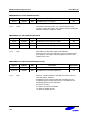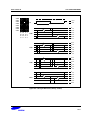
1
S3CC11B/FC11B
CalmRISC 16-Bit CMOS
MICROCONTROLLER
USER'S MANUAL
Revision 0
Important Notice
The information in this publication has been carefully
checked and is believed to be entirely accurate at the
time of publication. Samsung assumes no
responsibility, however, for possible errors or
omissions, or for any consequences resulting from
the use of the information contained herein.
Samsung reserves the right to make changes in its
products or product specifications with the intent to
improve function or design at any time and without
notice and is not required to update this
documentation to reflect such changes.
This publication does not convey to a purchaser of
semiconductor devices described herein any license
under the patent rights of Samsung or others.
Samsung makes no warranty, representation, or
guarantee regarding the suitability of its products for
any particular purpose, nor does Samsung assume
any liability arising out of the application or use of any
product or circuit and specifically disclaims any and
all liability, including without limitation any
consequential or incidental damages.
"Typical" parameters can and do vary in different
applications. All operating parameters, including
"Typicals" must be validated for each customer
application by the customer's technical experts.
Samsung products are not designed, intended, or
authorized for use as components in systems
intended for surgical implant into the body, for other
applications intended to support or sustain life, or for
any other application in which the failure of the
Samsung product could create a situation where
personal injury or death may occur.
Should the Buyer purchase or use a Samsung
product for any such unintended or unauthorized
application, the Buyer shall indemnify and hold
Samsung and its officers, employees, subsidiaries,
affiliates, and distributors harmless against all claims,
costs, damages, expenses, and reasonable attorney
fees arising out of, either directly or indirectly, any
claim of personal injury or death that may be
associated with such unintended or unauthorized use,
even if such claim alleges that Samsung was
negligent regarding the design or manufacture of said
product.
S3CC11B/FC11B 16-Bit CMOS Microcontroller
User's Manual, Revision 0
Publication Number: 20-S3-CC11B/FC11B-102004
© 2004 Samsung Electronics
All rights reserved. No part of this publication may be reproduced, stored in a retrieval system, or transmitted in any
form or by any means, electric or mechanical, by photocopying, recording, or otherwise, without the prior written
consent of Samsung Electronics.
Samsung Electronics' microcontroller business has been awarded full ISO-14001
certification (BVQ1 Certificate No. 9330). All semiconductor products are designed and
manufactured in accordance with the highest quality standards and objectives.
Samsung Electronics Co., Ltd.
San #24 Nongseo-Ri, Giheung- Eup
Yongin-City, Gyeonggi-Do, Korea
C.P.O. Box #37, Suwon 449-900
TEL:
FAX:
(82)-(331)-209-1907
(82)-(331)-209-1889
Home-Page URL:
Http://www.samsungsemi.com/
Printed in the Republic of Korea
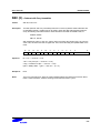
Preface
The S3CC11B/FC11B Microcontroller User's Manual is designed for application designers and programmers who are
using the S3CC11B/FC11B microcontroller for application development. It is organized in two main parts:
Part I
Programming Model
Part II
Hardware Descriptions
Part I contains software-related information to familiarize you with the microcontroller's architecture, programming
model, instruction set, and interrupt structure. It has seven chapters:
Chapter 1
Chapter 2
Chapter 3
Product Overview
Address Spaces
Calm16Core
Chapter 4
Chapter 5
Chapter 6
Exceptions
Memory Map
Instruction Set
Chapter 1, "Product Overview," is a high-level introduction to S3CC11B/FC11B with general product descriptions, as
well as detailed information about individual pin characteristics and pin circuit types.
Chapter 2, "Address Spaces," describes program and data memory spaces. Chapter 2 also describes ROM code
option.
Chapter 3, " Calm16Core," describes the special registers.
Chapter 4, " Exceptions ," describes the internal register file.
Chapter 5, " Memory Map," describes the S3CC11B/FC11B memory map structure in detail.
Chapter 6, " Instruction Set," describes the S3CC11B/FC11B instruction set structure in detail.
A basic familiarity with the information in Part I will help you to understand the hardware module descriptions in Part
II. If you are not yet familiar with the S3CK-series microcontroller family and are reading this manual for the first time,
we rec ommend that you first read Chapters 1–3 carefully. Then, briefly look over the detailed information in Chapters
4, 5 and 6. Later, you can reference the information in Part I as necessary.
Part II "hardware Descriptions," has detailed information about specific hardware components of the
S3CC11B/FC11B microcontroller. Also included in Part II are electrical, mechanical. It has 20 chapters:
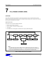
Chapter 7
Chapter 8
Chapter 9
Chapter 10
Chapter 11
Chapter 12
Chapter 13
Chapter 14
Chapter 15
Chapter 16
Chapter 17
PLL (Phase Locked Loop)
RESET and Power-Down
I/O Ports
Basic Timer
Watch Timer
8-bit Timer 0
16-Bit Timer 1 (8-Bit Timer A & B)
Serial I/O Interface
SSFDC (Solid State Floppy Disk Card)
10-Bit Analog-to-Digital Converter
CODEC
Chapter 18
Chapter 19
Chapter 20
Chapter 21
Chapter 22
Chapter 23
Chapter 24
Chapter 25
Chapter 26
LCD Controller / Driver
Battery Level Detector
8/16-Bit Serial Interface for
External Codec
CaimMAC1616
Program Memory Access Speed
Electrical Data
Mechanical Data
S3FC11B Flash MCU
Development Tools
One order form is included at the back of this manual to facilitate customer order for S3CC11B/FC11B
microcontrollers: the Flash Factory Writing Order Form.
You can photocopy this form, fill it out, and then forward it to your local Samsung Sales Representative.
S3CC11B/FC11B MICROCONTROLLER
iii
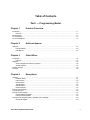
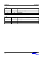
Table of Contents
Part I — Programming Model
Chapter 1
Product Overview
Introduction................................ ................................ ................................ ................................ ......... 1-1
Features................................ ................................ ................................ ................................ ..... 1-1
Block Diagram .................................................................................................................................... 1-3
Pin Assignment................................................................................................................................... 1-4
Pin Circuit Diagrams ............................................................................................................................ 1-9
Chapter 2
Address Spaces
Overview................................ ................................ ................................ ................................ ............. 2-1
Program Memory ................................ ................................ ................................ ......................... 2-2
Data Memory .............................................................................................................................. 2-4
Chapter 3
Calm16Core
Introduction................................ ................................ ................................ ................................ ......... 3-1
Features................................ ................................ ................................ ................................ ..... 3-1
Registers ............................................................................................................................................ 3-2
General Registers & Extension Registers ...................................................................................... 3-2
Special Registers ........................................................................................................................ 3-3
Pipeline Structure ................................................................................................................................ 3-4
Interrupts ............................................................................................................................................ 3-5
Chapter 4
Exceptions
Overview................................ ................................ ................................ ................................ ............. 4-1
Hardware Reset........................................................................................................................... 4-1
FIQ Exception................................ ................................ ................................ ............................. 4-2
IRQ Exception................................ ................................ ................................ ............................. 4-2
TRQ Exception............................................................................................................................ 4-2
SWI Exception ............................................................................................................................ 4-2
Break Exception.......................................................................................................................... 4-2
Interrupt Sources (IRQ) ........................................................................................................................ 4-3
Interrupt Structure................................................................................................................................ 4-4
Interrupt Control Register...................................................................................................................... 4-5
Interrupt Masking Register............................................................................................................ 4-5
Interrupt Proirity Register.............................................................................................................. 4-5
Interrupt Prority Registers (IPRH: 3F0008H, IPRL: 3F0009H) ................................................................... 4-8
Interrupt Id Register ................................ ................................ ................................ ..................... 4-9
S3CC11B/FC11B MICROCONTROLLER
v
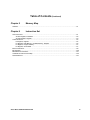
Table of Contents (Continued)
Chapter 5
Memory Map
Overview................................ ................................ ................................ ................................ ............. 5-1
Chapter 6
Instruction Set
ALU Instructions.................................................................................................................................. 6-1
ALUOP Register, Immediate................................ ................................ ................................ ......... 6-2
ALUOP Register, Register............................................................................................................ 6-3
Load Instructions................................ ................................ ................................ ................................ . 6-4
LD Regis ter, Register................................................................................................................... 6-4
LD Register, Data Memory / LD Data Memory, Register.................................................................. 6-5
LD Register, Program Memory...................................................................................................... 6-7
LD Register, # Immediate................................ ................................ ................................ ............. 6-7
Branch Instructions.............................................................................................................................. 6-8
Bit Operation....................................................................................................................................... 6-10
Miscellaneous Instructions ................................................................................................................... 6-11
CalmRISC16 Instruction Set Map.......................................................................................................... 6-12
Quick Reference.................................................................................................................................. 6-17
S3CC11B/FC11B MICROCONTROLLER
vii
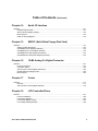
Table of Contents (Continued)
Part II — Hardware Descriptions
Chapter 7
PLL (Phase Locked Loop)
Overview................................ ................................ ................................ ................................ ............. 7-1
Chapter 8
RESET and Power-Down
Overview................................ ................................ ................................ ................................ ............. 8-1
Chapter 9
I/O Ports
Port Data Registers ................................ ................................ ................................ ............................. 9-1
Chapter 10
Basic Timer
Overview................................ ................................ ................................ ................................ ............. 10-1
Basic Timer & Watchdog Timer Block Diagram .............................................................................. 10-4
Chapter 11
Watch Timer
Overview................................ ................................ ................................ ................................ ............. 11-1
Watch Timer Block Diagram................................ ................................ ................................ ......... 11-3
Chapter 12
8-Bit Timer 0
Overview................................ ................................ ................................ ................................ ............. 12-1
Function Description .................................................................................................................... 12-2
Timer 0 Control Register (T0CON) ................................ ................................ ................................ . 12-3
Block Diagram ............................................................................................................................ 12-4
Chapter 13
16-Bit Timer 1 (8-Bit Timer A & B)
Overview................................ ................................ ................................ ................................ ............. 13-1
Interval Timer Function................................ ................................ ................................ ................. 13-1
Block Diagram ............................................................................................................................ 13-4
viii
S3CC11B/FC11B MICROCONTROLLER
Table of Contents (Continued)
Chapter 14
Serial I/O Interface
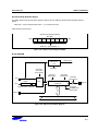
Overview................................ ................................ ................................ ................................ ............. 14-1
Programming Procedure............................................................................................................... 14-1
SIO Pre-Scaler Register (SIOPS).................................................................................................. 14-3
Block Diagram ............................................................................................................................ 14-3
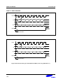
Serial I/O Timing Diagrams ........................................................................................................... 14-4
Chapter 15
SSFDC (Solid State Floppy Disk Card)
Overview................................ ................................ ................................ ................................ ............. 15-1
SSFDC Register Description ........................................................................................................ 15-3
SmartMedia Control Register (SMCON) ................................ ................................ ......................... 15-3
SmartMedia ECC Count Register (ECCNT) .................................................................................... 15-4
SmartMedia ECC Data Register (ECCDATA) ................................ ................................ ................. 15-4
SmartMedia ECC Result Data Register (ECCRST) ................................ ................................ ......... 15-4
Chapter 16
10-Bit Analog-To-Digital Converter
Overview................................ ................................ ................................ ................................ ............. 16-1
Function Description .................................................................................................................... 16-1
Conversion Timing ....................................................................................................................... 16-2
A/D Converter Control Register (ADCON10) ................................................................................... 16-2
Internal Reference Voltage Levels.................................................................................................. 16-3
Block Diagram ............................................................................................................................ 16-3
Chapter 17
Codec
Overview................................ ................................ ................................ ................................ ............. 17-1
Features................................ ................................ ................................ ................................ ..... 17-1
A/D Converter Control Register (ADCON)....................................................................................... 17-2
Chapter 18
LCD Controller/Driver
Overview................................ ................................ ................................ ................................ ............. 18-1
LCD Circuit Diagram .................................................................................................................... 18-2
LCD Display Registers................................ ................................ ................................ ................. 18-3
LCD Control Register (LCON) ....................................................................................................... 18-3
LCD Voltage Dividing Resistors................................ ................................ ................................ ..... 18-6
S3CC11B/FC11B MICROCONTROLLER
ix
Table of Contents (Continued)
Chapter 19
Battery Level Detector
Overview................................ ................................ ................................ ................................ ............. 19-1
Battery Level Detector Control Register (BLDCON) ................................ ................................ ......... 19-2
Chapter 20
8/16-Bit Serial Interface for External Codec
Overview................................ ................................ ................................ ................................ ............. 20-1
Programming Procedure............................................................................................................... 20-1
CSIO Control Register (CSIOCON)................................................................................................ 20-2
Chapter 21
CaimMAC1616
Introduction................................ ................................ ................................ ................................ ......... 21-1
Architecture Features .................................................................................................................. 21-1
Technology Features ................................................................................................................... 21-1
Block Diagram ............................................................................................................................ 21-2
Programming Model................................ ................................ ................................ ............................. 21-3
Multiplier and Accumulator Unit .................................................................................................... 21-4
Arithmetic Unit ............................................................................................................................ 21-7
Status Register 1 (MSR1) ............................................................................................................ 21-11
Ram Pointer Unit ................................ ................................ ................................ ......................... 21-13
Address Modification ................................................................................................................... 21-15
Data Memory Spaces and Organization................................ ................................ ......................... 21-19
Arithmetic Unit ............................................................................................................................ 21-21
Overflow Protection in Accumulators ................................ ................................ ............................. 21-22
External Condition Generation Unit................................................................................................ 21-24
Status Register 0 (MSR0) ............................................................................................................ 21-25
Status Register 2 (MSR2) ............................................................................................................ 21-27
Barrel Shifter and Exponent Unit ................................................................................................... 21-29
Barrel Shifter............................................................................................................................... 21-29
Shifting Operations ...................................................................................................................... 21-30
Exponent Block........................................................................................................................... 21-33
Instruction Set Map and Summary ........................................................................................................ 21-34
Addressing Modes....................................................................................................................... 21-34
Instruction Coding........................................................................................................................ 21-39
Quick Reference.......................................................................................................................... 21-55
Instruction Set................................ ................................ ................................ ................................ ..... 21-60
Glossary ................................ ................................ ................................ ................................ ..... 21-60
x
S3CC11B/FC11B MICROCONTROLLER
Table of Contents (Continued)
Chapter 22
Program Memory Access Speed
Overview................................ ................................ ................................ ................................ ............. 22-1
Chapter 23
Electrical Data
Overview................................ ................................ ................................ ................................ ............. 23-1
Chapter 24
Mechanical Data
Overview................................ ................................ ................................ ................................ ............. 24-1
Chapter 25
S3FC11B Flash MCU
Overview................................ ................................ ................................ ................................ ............. 25-1
Chapter 26
Development Tools
Overview................................ ................................ ................................ ................................ ............. 26-1
CalmSHINE: IDE (Integrated Development Environment).................................................................. 26-1
In-Circuit Emulator....................................................................................................................... 26-1
CalmRISC16 C-Compiler: CalmCC16................................ ................................ ............................. 26-1
CalmRISC16 Relocatable Assembler: Calm8ASM .......................................................................... 26-1
CalmRISC16 Linker: Calm8LINK ................................................................................................... 26-1
Emulation Probe Board Configuration .................................................................................................... 26-2
Use Clock Setting for External Clock Mode.................................................................................... 26-3
Sub Clock Setting ....................................................................................................................... 26-3
The Lowpass Filter for PLL ........................................................................................................... 26-3
Power Selection.......................................................................................................................... 26-4
Clock Selection........................................................................................................................... 26-4
JP1, JP2 Pin Assignment................................ ................................ ................................ ............. 26-5
JP11 Pin Assignment .................................................................................................................. 26-5
S3CC11B/FC11B MICROCONTROLLER
xi
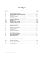
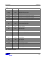
List of Figures
Figure
Number
Title
Page
Number
1-1
1-2
1-3
1-4
1-5
1-6
1-7
1-8
1-9
1-10
1-11
1-12
1-13
S3CC11B/FC11B Top Block Diagram ............................................................................... 1-3
S3CC11B/FC11B Pin Assignments (100-QFP-1420C) ........................................................ 1-4
S3CC11B/FC11B Pin Assignments (100-TQFP-1414) ........................................................ 1-5
Pin Circuit Type 1 ........................................................................................................... 1-9
Pin Circuit Type 2 (nRESET) ............................................................................................ 1-9
Pin Circuit Type 3 ........................................................................................................... 1-9
Pin Circuit Type 4 (P0.4-P0.7, P1, P2, P3.4-P3.7, P4.0)................................ ..................... 1-10
Pin Circuit Type 5 (P0.0-P0.3).......................................................................................... 1-10
Pin Circuit Type 6 (P3.0-P3.3).......................................................................................... 1-11
Pin Circuit Type 7 ........................................................................................................... 1-11
Pin Circuit Type 7 (P6, P7, P8, P9) .................................................................................. 1-12
Pin Circuit Type 9 (P4.1-P4.3, P5) .................................................................................... 1-12
Pin Circuit Type 10 (P4.4-P4.7) ........................................................................................ 1-13
2-1
2-2
Program Memory Configuration ........................................................................................ 2-2
Data Memory Configuration.............................................................................................. 2-4
3-1
Register Structure in CalmRISC16 .................................................................................... 3-2
4-1
4-2
4-3
Interrupt Sources (IRQ).................................................................................................... 4-3
Interrupt Structure ........................................................................................................... 4-4
Interrupt Priority Register (IPR) ................................ ................................ ......................... 4-8
5-1
Memory Mapped IO Registers.......................................................................................... 5-1
7-1
7-2
7-3
Phase-Locked Loop Circuit Diagram ................................ ................................ ................. 7-1
System Clock Circuit Diagram ................................ ................................ ......................... 7-4
External Loop Filter for PLL.............................................................................................. 7-5
9-1
Port Data Register Structure ............................................................................................ 9-1
10-1
Basic Timer & Watchdog Timer Block Diagram.................................................................. 10-4
11-1
Watch Timer Block Diagram ............................................................................................ 11-3
12-1
Timer 0 Functional Block Diagram .................................................................................... 12-4
13-1
Timer 1 Block Diagram .................................................................................................... 13-4
S3CC11B/FC11B MICROCONTROLLER
xiii
List of Figures (Continued)
Figure
Number
Title
Page
Number
14-1
14-2
14-3
14-4
SIO Pre-scaler Register (SIOPS)...................................................................................... 14-3
SIO Functional Block Diagram ................................ ................................ ......................... 14-3
Serial I/O Timing in Transmit/Receive Mode (Tx at falling, SIOCON.4 = 0) ............................ 14-4
Serial I/O Timing in Transmit/Receive Mode (Tx at rising, SIOCON.4 = 1) ............................. 14-4
15-1
15-2
Simple System Configuration ........................................................................................... 15-2
ECC Processor Block Diagram ........................................................................................ 15-5
16-1
16-2
16-3
16-4
A/D Converter Control Register (ADCON10)....................................................................... 16-2
A/D Converter Data Register (ADDATAH10/ADDATAL10) ................................................... 16-3
A/D Converter Functional Block Diagram ........................................................................... 16-3
Recommended A/D Converter Circuit for Highest Absolute Accuracy ................................... 16-4
17-1
17-2
CODEC Block Diagram ................................................................................................... 17-4
Single-Ended Input Application................................ ................................ ......................... 17-5
18-1
18-2
18-3
18-4
18-5
18-6
18-7
18-9
LCD Function Diagram .................................................................................................... 18-1
LCD Circuit Diagram ........................................................................................................ 18-2
LCD Display Register Organization................................................................................... 18-3
LCD Voltage Dividing Registers Connection....................................................................... 18-6
LCD Signal Waveforms (1/3 Duty, 1/3 Bias)....................................................................... 18-7
LCD Signal Waveforms (1/4 Duty, 1/3 Bias)....................................................................... 18-8
LCD Signal Waveforms (1/8 Duty, 1/4 Bias)....................................................................... 18-9
LCD Signal Waveforms (1/8 Duty, 1/5 Bias)....................................................................... 18-11
19-1
19-2
Block Diagram for Battery Level Detect ................................ ................................ ............. 19-1
Battery Level Detector Circuit and Control Register ............................................................ 19-2
20-1
20-2
20-3
SIO Block Diagram for External Codec.............................................................................. 20-4
8-Bit SIO Timing Diagram for External Codec ................................ ................................ ..... 20-5
16-Bit SIO Timing Diagram for External Codec ................................................................... 20-6
xiv
S3CC11B/FC11B MICROCONTROLLER
List of Figures (Continued)
Figure
Number
Title
Page
Number
21-1
21-2
21-3
21-4
21-5
21-6
21-7
21-8
21-9
21-10
21-11
21-12
21-13
21-14
21-15
21-16
21-17
21-18
21-19
21-20
21-21
21-22
21-23
CalmMAC1616 Block Diagram ................................ ................................ ......................... 21-2
Multiplier and Accumulator Unit Block Diagram.................................................................. 21-4
MAU Registers Configuration ........................................................................................... 21-6
Integer Division Example.................................................................................................. 21-9
Fractional Division Example................................ ................................ ............................. 21-10
MSR1 Register Configuration ........................................................................................... 21-11
RAM Pointer Unit Block Diagram...................................................................................... 21-14
Pointer Register and Index Register Configuration.............................................................. 21-15
Modulo Control Register Configuration............................................................................... 21-17
CalmMAC16 Data Memory Space Map................................ ................................ ............. 21-19
CalmMAC16 Data Memory Allocation ............................................................................... 21-20
Arithmetic Unit Block Diagram ................................ ................................ ......................... 21-22
Accumulator Register Configuration.................................................................................. 21-23
MSR0 Register Configuration ........................................................................................... 21-25
MSR2 Register Configuration ........................................................................................... 21-27
Barrel Shifter and Exponent Unit Block Diagram ................................................................ 21-29
Various Barrel Shifter Instruction Operation ....................................................................... 21-31
Indirect Addressing Example I (Single Read Operation) ...................................................... 21-34
Indirect Addressing Example II (Dual Read Operation) ........................................................ 21-35
Indirect Addressing Example III (Write Operation)............................................................... 21-36
Short Direct Addressing Example................................ ................................ ..................... 21-36
Long Direct Addressing Example...................................................................................... 21-37
Short Direct Associated Addressing Example.................................................................... 21-38
23-1
23-2
23-3
23-4
23-5
23-6
23-7
23-8
Operating Voltage Range................................ ................................ ................................ . 23-4
Input Timing for External Interrupts (Ports 0, Ports 4).......................................................... 23-5
Input Timing for RESET ................................................................................................... 23-5
Stop Mode Release Timing When Initiated by a nRESET.................................................... 23-6
Stop Mode(main) Release Timing Initiated by Interrupts...................................................... 23-7
Stop Mode(sub) Release Timing Initiated by Interrupts........................................................ 23-7
Clock Timing Measurement at XIN................................ ................................ ..................... 23-8
Clock Timing Measurement at XTIN ................................................................................... 23-9
24-1
24-2
100-QFP-1420C Package Dimensions .............................................................................. 24-2
100-TQFP-1414 Package Dimensions............................................................................... 24-3
25-1
25-2
S3FC11B Pin Assignments (100-QFP-1420C) ................................................................... 25-2
S3FC11B Pin Assignments (100-TQFP-1414).................................................................... 25-3
26-1
Emulation Probe Board Configuration ................................................................................ 26-2
S3CC11B/FC11B MICROCONTROLLER
xv
List of Tables
Table
Number
Titl e
Page
Number
1-1
S3CC11B/FC11B Pin Description................................ ................................ ..................... 1-6
4-1
Exceptions................................ ................................ ................................ ..................... 4-1
5-1
Registers ....................................................................................................................... 5-2
6-1
6-2
CalmRISC16 Instruction Set Map ................................ ................................ ..................... 6-12
Quick Reference................................ ................................ ................................ ............. 6-17
9-1
Port Data Register Summary ........................................................................................... 9-1
15-1
Control Register Description................................ ................................ ............................. 15-3
19-1
BLDCON Value and Detection Level ................................ ................................ ................. 19-2
21-1
Exponent Evaluation and Normalization Example............................................................... 21-33
23-1
23-2
23-3
23-4
23-5
23-6
23-7
23-8
23-9
23-10
Absolute Maximum Ratings ................................ ................................ ............................. 23-1
D.C. Electrical Characteristics ................................ ................................ ......................... 23-1
A.C. Electrical Characteristics ................................ ................................ ......................... 23-5
Data Retention Supply Voltage in Stop Mode .................................................................... 23-6
Main Oscillator Characteristics................................ ................................ ......................... 23-8
Sub Oscillator Frequency ................................................................................................ 23-9
BLD Electrical Characteristics.......................................................................................... 23-10
PLL Electrical Characteristics.......................................................................................... 23-10
10-Bit A/D Converter Electrical Characteristics ................................ ................................ . 23-10
ADC/DAC Electrical Characteristics ................................ ................................ ................. 23-11
25-1
Descriptions of Pins Used to Read/Write the FLASH ROM................................ ................. 25-4
S3CC11B/FC11B MICROCONTROLLER
xvii
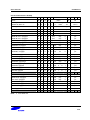
List of Instruction Descriptions
Instruction
Mnemonic
ADC (1)
ADC (2)
ADD (1)
ADD (2)
ADD (3)
ADD (4)
ADD (5)
ADD (6)
AND (1)
AND (2)
AND (3)
BITop
BNZD
BR
BRA EC
BREAK
BSRD
CLD
CLRSR
CMP (1)
CMP (2)
CMP (3)
CMPEQ (1)
CMPEQ (2)
CMPEQ (3)
COM
COP
DECC
DT
EXT
INCC
JMP (1)
JMP (2)
LD (1)
LD (2)
LD (3)
LD (4)
LD (5)
LD RExt
LDB (1)
LDB (2)
LDB (3)
LDB (4)
LDC
LD PC
LD SvR (1)
Full Instruction Name
Page
Number
Add with Carry Register....................................................................................... 6-21
Add with Carry Immediate .................................................................................... 6-22
Add Register ...................................................................................................... 6-23
Add Small Immediate.......................................................................................... 6-24
Add Immediate ................................................................................................... 6-25
Add Extended Register........................................................................................ 6-26
Add Immediate to Extended Register .................................................................... 6-27
Add 5-bit Immediate to Extended Register................................ ............................. 6-28
AND Register ................................ ................................ ................................ ..... 6-29
AND Small Immediate................................ ................................ ......................... 6-30
AND Large Immediate ................................ ................................ ......................... 6-31
BIT Operation ................................ ................................ ................................ ..... 6-32
Branch Not Zero with Autodecrement .................................................................... 6-33
Conditional Branch.............................................................................................. 6-34
Branch on External Condition............................................................................... 6-35
BREAK.............................................................................................................. 6-36
Branch Subroutine with Delay Slot........................................................................ 6-37
Coprocessor Load............................................................................................... 6-38
Clear SR ............................................................................................................ 6-39
Compare Register ............................................................................................... 6-40
Compare Immediate ............................................................................................ 6-41
Compare Short Immediate ................................................................................... 6-42
Compare Equal Extended Register ....................................................................... 6-43
Compare Equal Small Immediate.......................................................................... 6-44
Compare Equal Large Immediate.......................................................................... 6-45
Complement....................................................................................................... 6-46
Coprocessor....................................................................................................... 6-47
Decrement with Carry.......................................................................................... 6-48
Decrement and Test ............................................................................................ 6-49
Sign-Extend ....................................................................................................... 6-50
Increment with Carry ........................................................................................... 6-51
Jump Register .................................................................................................... 6-52
Jump Immediate ................................ ................................ ................................ . 6-53
Load Register ................................ ................................ ................................ ..... 6-54
Load Register ................................ ................................ ................................ ..... 6-55
Load Short Immediate ................................ ................................ ......................... 6-56
Load Immediate.................................................................................................. 6-57
Load Large Immediate................................ ................................ ......................... 6-58
Load Register Extension...................................................................................... 6-59
Load Byte Register Disp. ................................ ................................ ..................... 6-60
Load Byte Register Large Disp. ............................................................................ 6-61
Load Byte Register Indexed................................ ................................ ................. 6-62
Load Byte to R0 Register Disp. ............................................................................ 6-63
Load Code.......................................................................................................... 6-64
Load Program Counter................................ ................................ ......................... 6-65
Load from Saved Register .................................................................................... 6-66
S3CC11B/FC11B MICROCONTROLLER
xix
List of Instruction Descriptions (Contin ued)
Instruction
Mnemonic
LD SvR (2)
LD SR
LDW (1)
LDW (2)
LDW (3)
LDW (4)
LDW (5)
LDW (6)
LDW (7)
MUL
NOP
OR (1)
OR (2)
OR (3)
POP (1)
POP (2)
PUSH (1)
PUSH (2)
RETD
RET_FIQ
RET_IRQ
RET_SWI
RL
RR
RRC
SBC (1)
SBC (2)
SETSR
SLB
SR
SRA
SRB
SUB (1)
SUB (2)
SUB (3)
SUB (4)
SUB (5)
SWI
SYS
TST (1)
TST (2)
TST (3)
TSTSR
XOR (1)
XOR (2)
XOR (3)
xx
Full Instruction Name
Page
Number
Load to Saved Register........................................................................................ 6-67
Load Status Register........................................................................................... 6-68
Load Word Stack Disp. ....................................................................................... 6-69
Load Word Register Small Disp............................................................................ 6-70
Load Word Register Disp. .................................................................................... 6-71
Load Word Register Indexed ................................................................................ 6-72
Load Word Register Small Disp............................................................................ 6-73
Load Word Register Disp. .................................................................................... 6-74
Load Word Register Indexed ................................................................................ 6-75
Multiplication...................................................................................................... 6-76
No Operation...................................................................................................... 6-77
OR Register ....................................................................................................... 6-78
OR Small Immediate ........................................................................................... 6-79
OR Large Immediate ........................................................................................... 6-80
Load Register from Stack .................................................................................... 6-81
Load Register from Stack .................................................................................... 6-82
Load Register to Stack ........................................................................................ 6-83
Load Register to Stack ........................................................................................ 6-84
Ret. from Subroutine with Delay Slot................................ ................................ ..... 6-85
Return from Fast Interrupt .................................................................................... 6-86
Return from Interrupt............................................................................................ 6-87
Return from Software Interrupt.............................................................................. 6-88
Rotate Left ................................ ................................ ................................ ......... 6-89
Rotate Right ....................................................................................................... 6-90
Rotate Right with Carry........................................................................................ 6-91
Subtract with Carry Register ................................................................................ 6-92
Subtract with Carry Immediate ................................ ................................ ............. 6-93
Set SR............................................................................................................... 6-94
Shift Left Byte................................ ................................ ................................ ..... 6-95
Shift Right.......................................................................................................... 6-96
Shift Right Arithmetic .......................................................................................... 6-97
Shift Right Byte .................................................................................................. 6-98
Subtract Register ................................................................................................ 6-99
Subtract Small Immediate.................................................................................... 6-100
Subtract Extended Register ................................ ................................ ................. 6-101
Subtract Large Immediate .................................................................................... 6-102
Subtract 5-bit Immediate...................................................................................... 6-103
Software Interrupt ................................................................................................ 6-104
System .............................................................................................................. 6-105
Test Register...................................................................................................... 6-106
Test Small Immediate.......................................................................................... 6-107
Test Large Immediate.......................................................................................... 6-108
Test SR ................................ ................................ ................................ ............. 6-109
XOR Register...................................................................................................... 6-110
XOR Small Immediate ................................ ................................ ......................... 6-111
XOR Large Immediate.......................................................................................... 6-112
S3CC11B/FC11B MICROCONTROLLER
S3CC11B/FC11B
1
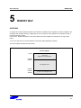
PRODUCT OVERVIEW
PRODUCT OVERVIEW
INTRODUCTION
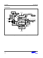
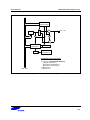
The S3FC11B is a calmRISC16 and MAC1616 core-based CMOS single-chip microcontroller. It contains ROM,
RAM, 77 I/O pins, programmable 8/16-bit timer/counters, CODEC, PLL, 4-ch A/D converter, 36SEG x 8COM LCD
controller/driver, and etc. The S3FC11B can be used for dedicated control functions in a variety of applications, and
is especially designed for application with voice synthesizer, voice recognition, or etc.
FEATURES
Memory
One 16-Bit Timer/Counter 1
•
24K x 16 bits program memory (mtp flash ROM)
•
One 16-bit timer/counter mode
•
•
8K x 16 bits data memory (mtp flash ROM)
10K x 8 bits data memory (excluding LCD RAM)
•
Two 8-bit timer/counters A/B mode
Watch Timer
77 I/O Pins
•
•
•
Interval time: 3.91ms, 0.25S, 0.5S, and 1S at
32.768 kHz
•
0.5/1/2/4 kHz selectable buzzer output
I/O: 33 pins
I/O 44 pins (Sharing with segment drive output)
SSFDC Interface Logic
LCD Controller/Driver
•
•
36 segments and 8 common terminals
•
•
3, 4 and 8 common selectable
Internal resistor circuit for LCD bias
Two selection pins (nCE0, nCE1)
8-Bit Basic Timer
•
Programmable interval timer
•
8 kinds of clock sourc e
•
Watch-dog timer's clock source
(overflow of 8-bit counter)
8-Bit Serial Interface
•
Four programmable operating modes
8/16-Bit Serial Interface for External Codec
Watchdog Timer
•
Internal/External clock source selectable
•
•
Two programmable operating modes
System reset when 3-bit counter overflow
One 8-Bit Timer/Counter 0
•
Programmable interval timer
•
External event counter function
•
PWM function and capture function
1-1
PRODUCT OVERVIEW
S3CC11B/FC11B
FEATURES (Continued)
Battery Level Detector
Operating Voltage Range
•
Programmable low voltage detector
•
•
Two criteria voltage (2.45 V, 2.70 V)
2.0 V to 3.6 V
Operating Temperature Range
Phase -Locked Loop (PLL)
•
•
–25 °C to +85 °C
Programmable clock synthesizer
Current Consumption
Codec
•
Sub idle current: 6.0 uA at V DD = 3.3V
•
14-bit A/D converter, 14-bit D/A converter
•
3.6 kHz –11 kHz sampling frequency
Package Type
•
3.0 V–3.6 V operating voltage range
•
Analog to Digital Converter (10-bit resolution)
•
4-channel analog inputs
•
•
25uS conversion time
3.0 V–3.6 V operation voltage range
Two Power-Down Modes
•
Idle: Only CPU clock stops
•
Stop: Selected system clock and CPU clock stop
Oscillation Sources
•
Crystal or ceramic for main clock
•
•
Programmable oscillation sources for main clock
32.768 kHz crystal oscillation circuit for sub clock
•
CPU clock divider circuit (divided by 1, 2, 4, or 8)
Instruction Execution Times
•
Main clocks:
30 ns at 32 MHz when 1 cycle instructions
60 ns at 32 MHz when 2 cycle instructions
•
Sub clocks (32.768 kHz):
30.52 us when 1 cycle instructions
61.04 us when 2 cycle instructions
1-2
100-QFP, 100-TQFP package
S3CC11B/FC11B
PRODUCT OVERVIEW
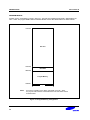
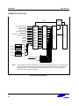
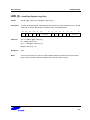
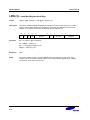
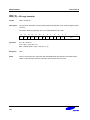
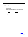
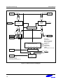
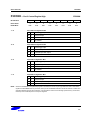
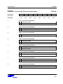
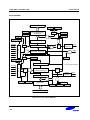
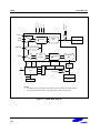
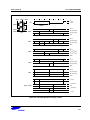
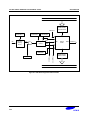
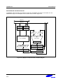
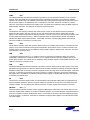
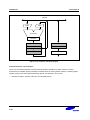
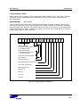
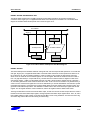
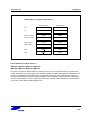
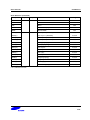
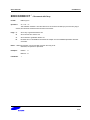
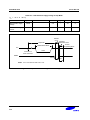
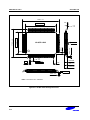
BLOCK DIAGRAM
X IN X OUT XTin XTout
VDD1, VDD2,
VDD3
VSS1, VSS2, VSS3
AVDD1, AVSS1
P5.0-P5.7/
SEG7-SEG14
P4.0/CDR
P4.1/CDX/SEG0
P4.2/CFS/SEG1
P4.3/CCLK/SEG2
P4.4-P4.7/INT4-INT7/
SEG3-SEG6
P3.0-P3.2/
CIN0-CIN2
P3.3/T0CLK
P3.4/T0OUT/T0PWM/T0CAP
P3.5/BUZ/T1CLK
P3.6/TAOUT
P3.7/TBOUT
WDT
BASIC
TIMER
PORT 7
P7.0-P7.7/
SEG23-SEG30
PORT 8
P8.0-P8.4/
SEG31-SEG35
PORT 9
P9.0-P9.7/
COM7-COM0
PORT 6
PORT 5
CalmRISC CPU
SI/P0.5
SO/P0.6
SCK/P0.7
SIO
PORT 4
T0CLK/P3.3
TIMER 0
TIMER A
TIMER B
PORT 3
P2.0/nWE
P2.1/nRE
P2.2/WP
P2.3/ R/nB
P2.4/ALE
P2.5/CLE
P2.6/nCE0
P2.7/nCE1
PORT 2
P1.0-P1.7
I/O0-I/O7
PORT 1
P0.0-P0.3/
INT0-INT3
P0.4
P0.5/SI
P0.6/SO
P0.7/SCK
PORT 0
I/O0 / P1.0-I/O7 /P1.7
CLE, ALE,WP,nWE,nRE,nCE0,nCE1
R/nB
X-Memory
Y-Memory
(6144 Bytes) (4096 Bytes)
RAM
(196 Bytes)
MAC1616
(DSP)
T0OUT/T0PWM/
T0CAP/P3.4
T1CLK/P3.5/BUZ
TAOUT/P3.6
TBOUT/P3.7
WATCH
TIMER
BUZ/P3.5/T1CLK
SIO for
ext. Codec
CDR/P4.0
CDX/P4.1/SEG0
CFS/P4.2/SEG1
CCLK/P4.3/SEG2
A/DC
Flash ROM
(32k x 16)
TIMER1
P6.0-P6.7/
SEG15-SEG22
MAIN OSC.
SUB OSC.
PLL
AD0-AD2/P3.0-P3.2
AD3/P3.3/T0CLK
BLD
CODEC
AVDD2
AVSS2
ADINP
ADINN
ADGAIN
DAOUT
VREFOUT
COM0-COM7/P9.7-P9.0
Smartmedia
Interface
LCD Driver/
Controller
SEG0-SEG35/P4.1-P8.4
VLC1
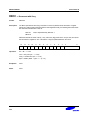
Figure 1-1. S3CC11B/FC11B Top Block Diagram
1-3
PRODUCT OVERVIEW
S3CC11B/FC11B
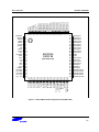
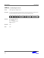
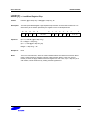
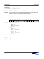
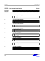
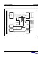
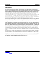
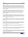
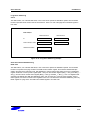
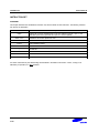
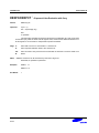
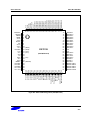
100
99
98
97
96
95
94
93
92
91
90
89
88
87
86
85
84
83
82
81
P0.5/SI
P0.6/SO
P0.7/SCK
VLC1
COM0/P9.7
COM1/P9.6
COM2/P9.5
COM3/P9.4
COM4/P9.3
COM5/P9.2
COM6/P9.1
COM7/P9.0
SEG35/P8.4
SEG34/P8.3
SEG33/P8.2
SEG32/P8.1
SEG31/P8.0
SEG30/P7.7
SEG29/P7.6
SEG28/P7.5
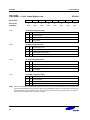
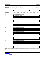
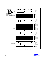
PIN ASSIGNMENT
1
2
3
4
5
6
7
8
9
10
11
12
13
14
15
16
17
18
19
20
21
22
23
24
25
26
27
28
29
30
S3CC11B/
S3FC11B
(100-QFP-1420C)
80
79
78
77
76
75
74
73
72
71
70
69
68
67
66
65
64
63
62
61
60
59
58
57
56
55
54
53
52
51
SEG27/P7.4
SEG26/P7.3
SEG25/P7.2
SEG24/P7.1
SEG23/P7.0
SEG22/P6.7
SEG21/P6.6
SEG20/P6.5
SEG19/P6.4
SEG18/P6.3
SEG17/P6.2
SEG16/P6.1
SEG15/P6.0
SEG14/P5.7
VDD2
VSS2
SEG13/P5.6
SEG12/5.5
SEG11/P5.4
SEG10/P5.3
SEG9/P5.2
SEG8/P5.1
SEG7/P5.0
SEG6/P4.7/INT7
SEG5/P4.6/INT6
SEG4/P4.5/INT5
SEG3/P4.4/INT4
SEG2/P4.3/CCLK
SEG1/P4.2/CFS
SEG0/P4.1/CDX
P1.5/ I/O5
P1.6/ I/O6
P1.7/ I/O7
P2.0/nWE
P2.1/nRE
P2.2/WP
P2.3/ R/nB
P2.4/ALE
P2.5/CLE
P2.6/nCE0
P2.7/nCE1
P3.0/AD0
P3.1/AD1
P3.2/AD2
P3.3/AD3/T0CLK
P3.4/T0PWM
P3.5/BUZ/T1CLK
P3.6/TAOUT
P3.7/TBOUT
P4.0/CDR
31
32
33
34
35
36
37
38
39
40
41
42
43
44
45
46
47
48
49
50
VDD3
VSS3
VREFOUT
ADGAIN
ADINN
ADINP
AVDD2
AVSS2
DAOUT
LPF
AVDD1
AVSS1
P0.4
P0.3/INT3
VDD1
VSS1
Xout
XIN
TEST
XTin
XTout
nRESET
P0.2/INT2
P0.1/INT1
P0.0/INT0
P1.0/ I/O0
P1.1/ I/O1
P1.2/ I/O2
P1.3/ I/O3
P1.4/ I/O4
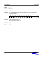
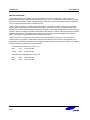
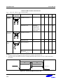
Figure 1-2. S3CC11B/FC11B Pin Assignments (100-QFP-1420C)
1-4
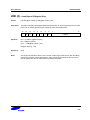
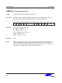
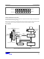
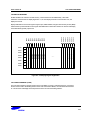
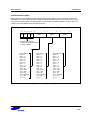
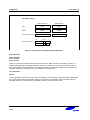
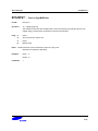
PRODUCT OVERVIEW
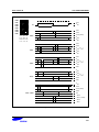
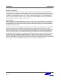
S3CC11B/
S3FC11B
(100-TQFP-1414)
75
74
73
72
71
70
69
68
67
66
65
64
63
62
61
60
59
58
57
56
55
54
53
52
51
SEG24/P7.1
SEG23/P7.0
SEG22/P6.7
SEG21/P6.6
SEG20/P6.5
SEG19/P6.4
SEG18/P6.3
SEG17/P6.2
SEG16/P6.1
SEG15/P6.0
SEG14/P5.7
VDD2
VSS2
SEG13/P5.6
SEG12/5.5
SEG11/P5.4
SEG10/P5.3
SEG9/P5.2
SEG8/P5.1
SEG7/P5.0
SEG6/P4.7/INT7
SEG5/P4.6/INT6
SEG4/P4.5/INT5
SEG3/P4.4/INT4
SEG2/P4.3/CCLK
26
27
28
29
30
31
32
33
34
35
36
37
38
39
40
41
42
43
44
45
46
47
48
49
50
1
2
3
4
5
6
7
8
9
10
11
12
13
14
15
16
17
18
19
20
21
22
23
24
25
P1.2/ I/O2
P1.3/ I/O3
P1.4/ I/O4
P1.5/ I/O5
P1.6/ I/O6
P1.7/ I/O7
P2.0/nWE
P2.1/nRE
P2.2/WP
P2.3/ R/nB
P2.4/ALE
P2.5/CLE
P2.6/nCE0
P2.7/nCE1
P3.0/AD0
P3.1/AD1
P3.2/AD2
P3.3/AD3/T0CLK
P3.4/T0PWM
P3.5/BUZ/T1CLK
P3.6/TAOUT
P3.7/TBOUT
P4.0/CDR
SEG0/P4.1/CDX
SEG1/P4.2/CFS
VREFOUT
ADGAIN
ADININ
ADINP
AVDD2
AVSS2
DAOUT
LPF
AVDD1
AVSS1
P0.4
P0.3/INT3
VDD1
VSS1
Xout
Xin
TEST
XTin
XTout
nRESET
P0.2/INT2
P0.1/INT1
P0.0/INT0
P1.0/ I/O0
P1.1/ I/O1
100
99
98
97
96
95
94
93
92
91
90
89
88
87
86
85
84
83
82
81
80
79
78
77
76
VSS3
VDD3
P0.5/SI
P0.6/SO
P0.7/SCK
VLC1
COM0/P9.7
COM1/P9.6
COM2/P9.5
COM3/P9.4
COM4/P9.3
COM5/P9.2
COM6/P9.1
COM7/P9.0
SEG35/P8.4
SEG34/P8.3
SEG33/P8.2
SEG32/P8.1
SEG31/P8.0
SEG30/P7.7
SEG29/P7.6
SEG28/P7.5
SEG27/P7.4
SEG26/P7.3
SEG25/P7.2
S3CC11B/FC11B
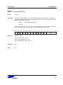
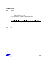
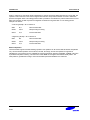
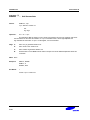
Figure 1-3. S3CC11B/FC11B Pin Assignments (100-TQFP-1414)
1-5
PRODUCT OVERVIEW
S3CC11B/FC11B
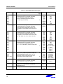
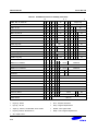
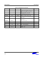
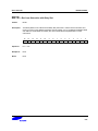
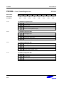
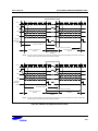
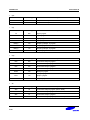
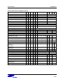
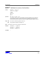
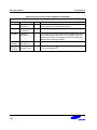
Table 1-1. S3CC11B/FC11B Pin Description
Name
Type
P0.0
P0.1
P0.2
P0.3
P0.4
P0.5
P0.6
P0.7
P1.0 – P1.7
I/O
P2.0
P2.1
P2.2
P2.3
P2.4
P2.5
P2.6
P2.7
P3.0
P3.1
P3.2
P3.3
P3.4
P3.5
P3.6
P3.7
I/O
P4.0
P4.1
P4.2
P4.3
P4.4 – P4.7
I/O
P5.0 – P5.6
I/O
P5.7
P6.0 – P6.7
I/O
P7.0 – P7.7
I/O
NOTE:
1-6
I/O
I/O
Description
I/O port with bit programmable pins;
Schmitt trigger input or push-pull, open-drain
output and software assignable pull-ups;
P0.0-P0.3 is alternatively used for external
interrupt input (noise filters).
Circuit
Type
5
4
I/O port with nibble-programmable pins;
Schmitt trigger input or push-pull, open-drain
output and software assignable pull-ups; Also
configurable as smartmedia interface lines I/O0 –
I/O7.
I/O port with bit-programmable pins;
Schmitt trigger input or push-pull, open-drain
output and software assignable pull-ups; Also
configurable as smartmedia interface lines nWE,
nRE, WP, R/nB, ALE, CLE, nCE0, and nCE1.
4
I/O port with bit-programmable pins;
Schmitt trigger input or push-pull, open-drain
output and software assignable pull-ups.
P3.0 – P3.3 is alternatively used for analog input.
6
4
4
I/O port with bit-programmable pins; Schmitt
trigger input or push-pull, open-drain output and
software assignable pull-ups. P4.4 – P4.7 is
alternatively used for external interrupt input
(noise filters, interrupt enable control).
I/O port with bit-programmable pins;
Schmitt trigger input or push-pull, open-drain
output and software assignable pull-ups.
I/O port with nibble-programmable pins; Schmitt
trigger input or push-pull output and software
assignable pull-ups.
Same general characteristics as port6.
The parentheses are a pin num ber of 100 -TQFP package.
4
9
10
9
8
8
Number
Shared Pins
25(23)
24(22)
23(21)
14(12)
13(11)
100(98)
99(97)
98(96)
26 – 33
(24–31)
INT0
INT1
INT2
INT3
–
SI
SO
SCK
I/O0 - I/O7
34(32)
35(33)
36(34)
37(35)
38(36)
39(37)
40(38)
41(39)
42(40)
43(41)
44(42)
45(43)
46(44)
47(45)
48(46)
49(47)
nWE
nRE
WP
R/nB
ALE
CLE
nCE0
nCE1
AD0
AD1
AD2
AD3/T0CLK
T0OUT/T0PWM/T0
CAP
BUZ/T1CLK
TAOUT
TBOUT
CDR
CDX/SEG0
CFS/SEG1
CCLK/SEG2
INT4-INT7/
SEG3 -SEG6
SEG7–SEG13
50(48)
51(49)
52(50)
53(51)
54 – 57
(52–55)
58 – 64
(56–62)
67(65)
68 – 75
(66–73)
76 – 83
(74–81)
SEG14
SEG15–SEG22
SEG23–SEG30
S3CC11B/FC11B
PRODUCT OVERVIEW
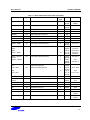
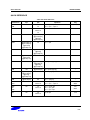
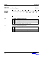
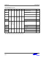
Table 1 -1. S3CC11B/FC11B Pin Description (Continued)
Name
Type
Description
Circuit
Type
Number
Shared Pins
P8.0 – P8.4
I/O
Same general characteristics as port6.
8
84 – 88
(82–86)
SEG31–
SEG35
P9.0 – P9.7
I/O
Same general characteristics as port6.
8
89 – 96
(87–94)
COM7–COM0
I
Analog negative input pin.
–
5(3)
–
I
ADINN
ADINP
Analog positive input pin.
–
6(4)
–
ADGAIN
I/O
Analog input gain control pin.
–
4(2)
–
VREFOUT
O
Vref output pin.
–
3(1)
–
DAOUT
O
Digital to analog converter output pin.
–
9(7)
–
LPF
I/O
PLL loop filter pin
–
10(8)
–
COM0 – COM7
I/O
LCD common data output pins.
8
96–89
(94–87)
P9.7-P9.0
SEG0
SEG1
SEG2
SEG3 – SEG6
I/O
LCD segment data output pins.
9
51(49)
52(50)
53(51)
54 – 57
(52–55)
P4.1/CDX
P4.2/CFS
P4.3/CCLK
P4.4-P4.7/
INT4-INT7
SEG7 – SEG13
SEG14
SEG15 – SEG35
I/O
P5.0-P5.6
8
58–64
(56–62)
67(65)
68–88
(66–86)
LCD power supply pins.
–
97(95)
–
External interrupt input pins.
5
P0.0 - P0.2
10
25–23
(23–21)
14(12)
54 – 57
(52–55)
VLC1
10
–
INT0 – INT2
I/O
LCD segment data output pins.
INT3
INT4 – INT7
9
P5.7
P6.0-P8.4
P0.3
P4.4 – P4.7
T1CLK
I/O
Timer 1/A external clock input pin.
4
47(45)
P3.5/BUZ
TAOUT
TBOUT
I/O
Timer 1/A and B clock output pins.
4
48(46)
49(47)
P3.6
P3.7
BUZ
I/O
Buzzer signal output pin.
4
47(45)
P3.5/T1CLK
SI
I/O
Serial data input pin.
4
100(98)
P0.5
SO
I/O
Serial data output pin.
4
99(97)
P0.6
SCK
I/O
Serial I/O interface clock signal pin.
4
98(96)
P0.7
T0OUT
I/O
Timer0’s interval output pin.
4
46(44)
P3.4/T0PWM/
T0CAP
T0PWM
I/O
Timer0’s PWM output pin.
4
46(44)
P3.4/T0OUT/
T0CAP
NOTE:
The parentheses are a pin number of 100 -TQFP package.
1-7
PRODUCT OVERVIEW
S3CC11B/FC11B
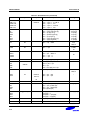
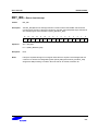
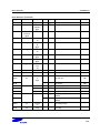
Table 1 -1. S3CC11B/FC11B Pin Description (Continued)
Name
Type
Description
Circuit
Type
4
T0CAP
I/O
Timer0’s Capture input pin.
T0CLK
nWE
nRE
WP
R/nB
ALE
CLE
nCE0
nCE1
I/O0 – I/O7
I/O
I/O
I/O
I/O
I/O
I/O
I/O
I/O
I/O
I/O
Timer0’s external clock input pin.
Write enable pin.
Read enable pin.
Write protect pin.
Ready and busy status pin.
Address latch enable pin.
Command latch enable pin.
Chip enable 0 pin.
Chip enable 1 pin.
Smartmedia interface lines.
6
4
4
4
4
4
4
4
4
4
AD0 – AD2
I/O
Analog input pins for A/D converter.
6
AD3
CDR
CDX
CFS
CCLK
AV DD1,
AV SS1
AV DD2,
AV SS2
nRESET
XTin,XTout
Receive data input pin for external codec.
Transmit data output pin for external codec.
Frame sync pulse for external codec.
Master and bit clock for external codec.
Analog power pins for PLL block.
4
9
9
9
–
–
Analog power pins for CODEC block.
–
I
–
System reset pin.
Crystal oscillator pins for sub clock.
2
–
Xin, Xout
–
Main oscillator pins.
–
TEST
VDD1 , VSS1
I
–
Input pin for test.(must be connected to V SS)
Power input pins for CPU.
–
–
VDD2 , VSS2
–
Power input pins for peripheral block.
–
VDD3 , VSS3
–
Power input pins for peripheral block.
–
NOTE:
1-8
I/O
I/O
I/O
I/O
–
The parentheses are a pin number o f 100-TQFP package.
Number Shared Pins
46(44)
45(43)
34(32)
35(33)
36(34)
37(35)
38(36)
39(37)
40(38)
41(39)
26 – 33
(24–31)
42 – 44
(40–42)
45(43)
50(48)
51(49)
52(50)
53(51)
11, 12
(9, 10)
7, 8
(5, 6)
22(20)
20, 21
(18, 19)
18, 17
(16, 15)
19(17)
15, 16
(13, 14)
66, 65
(64, 63)
2,1
(99,100)
P3.4/T0OUT/
T0PWM
P3.3/AD3
P2.0
P2.1
P2.2
P2.3
P2.4
P2.5
P2.6
P2.7
P1.0 – P1.7
P3.0 – P3.2
P3.3/T0CLK
P4.0
P4.1/SEG0
P4.2/SEG1
P4.3/SEG2
–
–
–
–
–
–
–
–
–
S3CC11B/FC11B
PRODUCT OVERVIEW
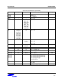
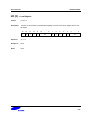
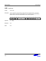
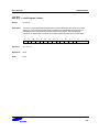
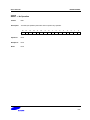
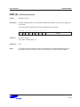
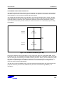
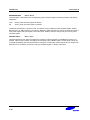
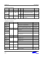
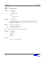
PIN CIRCUIT DIAGRAMS
VDD
VDD
P-CHANNEL
PULL-UP
RESISTOR
IN
N-CHANNEL
IN
SCHMITT TRIGGER
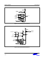
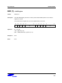
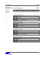
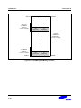
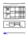
Figure 1-4. Pin Circuit Type 1
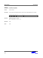
Figure 1-5. Pin Circuit Type 2 (nRESET)
VDD
Data
P-Channel
Out
Output
Disable
N-Channel
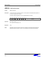
Figure 1-6. Pin Circuit Type 3
1-9
PRODUCT OVERVIEW
S3CC11B/FC11B
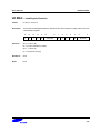
V DD
Pull-up
Resistor
VDD
Resistor
Enable
Open Drain
P-CH
Data
I/O
N-CH
Output
Disable
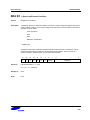
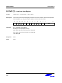
Figure 1-7. Pin Circuit Type 4 (P0.4-P0.7, P1, P2, P3.4-P3.7, P4.0)
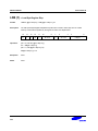
V DD
VDD
Pull-up
Resistor
Resistor
Enable
Open Drain
P-CH
Data
I/O
N-CH
Output
Disable
External
Interrupt
Input
Noise
Filter
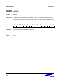
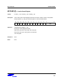
Figure 1-8. Pin Circuit Type 5 (P0.0-P0.3)
1-10
S3CC11B/FC11B
PRODUCT OVERVIEW
VDD
Pull-up
Enable
V DD
Open Drain
Enable
P-CH
I/O
Out Data
N-CH
Output
Disable
Digital In
Analog In
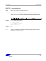
Figure 1-9. Pin Circuit Type 6 (P3.0-P3.3)
VDD
Pull-up
Resistor
Pull-up Enable
Select
VDD
Port Data
Alternative Signal
M
U
X
Data
In/Out
Open-Drain
Output Disable
Alternative Input
VSS
Normal Input
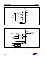
Figure 1-10. Pin Circuit Type 7
1-11
PRODUCT OVERVIEW
S3CC11B/FC11B
V DD
Pull-up
Resistor
Resistor
Enable
Data
Output
Disable 1
COM/SEG
Output
Disable 2
Circuit
Type 3
I/O
Circuit
Type 7
Figure 1-11. Pin Circuit Type 7 (P6, P7, P8, P9)
V DD
VDD
Pull-up
Resistor
Resistor
Enable
Open-Drain
P-CH
Data
I/O
N-CH
Output
Disable
SEG
Output
Disable
Circuit
Type 7
Figure 1-12. Pin Circuit Type 9 (P4.1-P4.3, P5)
1-12
S3CC11B/FC11B
PRODUCT OVERVIEW
V DD
VDD
Pull-up
Resistor
Resistor
Enable
Open Drain
P-CH
Data
I/O
N-CH
Output
Disable
Circuit
Type 7
SEG
Output
Disable
External
Interrupt
Input
Noise
Filter
Figure 1-13. Pin Circuit Type 10 (P4.4-P4.7)
1-13
PRODUCT OVERVIEW
S3CC11B/FC11B
NOTES
1-14
S3CC11B/FC11B
2
ADDRESS SPACE
ADDRESS SPACE
OVERVIEW
CalmRISC16 has 21-bit program address lines, PA[20:0] (equivalent to PC[21:1]), which supports up to 32K word of
program memory.
The 32K word program memory space is divided into 24K word internal program memory and 8K word Data Memory
(Data ROM) area.
CalmRISC16 also has 22-bit data memory address lines, DA[21:0], which supports up to 10K byte.
Memory configuration in CalmRISC16 side
Data Memory:
10K byte internal data memory
Program Memory:
24K word internal program memory
8K word data memory (Data ROM: YROM)
Memory configuration in CalmMAC24 side
Data Memory:
X-Memory area - 3K word internal memory (6K byte)
Y-Memory area - 2K word internal memory (4K byte)
Program Memory:
24K word internal program memory
8K word data memory (Data ROM: YROM)
2-1
ADDRESS SPACE
S3CC1 1B/FC11B
PROGRAM MEMORY
Program memory configuration is shown in Figure 2-1. The total size of ROM (Program ROM + Data ROM) is the
32K × 16 bits. The program ROM’s address is 0000H–BFFEH and the data ROM's address is C000H–FFFEH.
3FFFFEH
Not used
00FFFEH
Data ROM
00BFFEH
Program Memory
000000H
Byte
NOTE:
The total size of ROM (Program ROM + Data ROM) is the 32K × 16bits.
The program ROM's address is 0000H-BFFEH and the data ROM's address
is C000H-FFFEH.
Figure 2-1. Program Memory Configuration
2-2
S3CC11B/FC11B
ADDRESS SPACE
DATA MEMORY
Data memory configuration is shown in Figure 2.2. CalmMAC16 only can access the internal data memory and if the
memory request tries to access non-existent memory area, FIQ(Fast Interrupt request) is generated. In this case, if
FE bit in CalmRISC16’s SR register is 1, the violation service routine is called and served. CalmRISC16 can access
the internal data memory. But the FIQ is not used in the S3CC11B. The address of the CalmRISC16 consists of 8
bits, while the address of the MAC1616 consists of 16bits. So, if the address of the CalmRISC16 is E800H, the
address of the MAC1616 is 7400H. Program ROM can be accessed in the view of ROM (with LDC instruction) that
has 0000–BFFEH address. Also and in the view of RAM (with LDB, LDW instructions) that has same address.
Data ROM can be accessed in the view of ROM (with LDC instruction) that has C000 – FFFEH address. Also and in
the view of RAM (with LDB, LDW instructions) that has 11000 – 14FFFH address. Of course, Data ROM can be
accessed by MAC1616. (The address ranges are 8800H to A7FFH.)
The memory violation (access the non-existent area) FIQ can be also generated.
2-3
ADDRESS SPACE
S3CC1 1B/FC11B
Address of
CalmRISC16
Address of
MAC1616
3FFFFEH
Not used
3F00A4H
3F00A3H
3F0080H
3F007FH
3F0000H
3EFFFFH
LCD Display Registers
I/O Area
Control Registers
Not used
015000H
014FFFH
011000H
010FFFH
010000H
00FFFFH
00E800H
00E7FFH
Data ROM
Y-Memory
(Data RAM)
X-Memory
(Data RAM)
A7FFH
8800H
87FFH
8000H
7FFFH
7400H
Not used
00BFFFH
.7
.15
.7
7400H
.15
7401H
0E803H
0E802H
0E801H
0E800H
.7
.15
.7
.15
.6 .5 . 4 .3 .2
.14 .13 .12 .11 .10
.6 .5 . 4 .3 .2
.14 .13 .12 .11 .10
-MAC1616-
.1
.9
.1
.9
.0
.8
.0
.8
.6 .5 . 4 .3 .2 . 1
.14 .13 .12 .11 .10 . 9
.6 .5 . 4 .3 .2 . 1
.14 .13 .12 .11 .10 . 9
-CalmRISC16-
.0
.8
.0
.8
Program ROM
000000H
Byte
NOTES:
1. The address of the calmRISC consists of 8-bits, while the address of the MAC1616 consists of 16-bits.
2. The total size of ROM (Program ROM + Data ROM) is the 32K x 16bits. The program ROM's address is
0000H-BFFFH and the data ROM's address is C000H-FFFEH.
3. The data of program memroy (Program ROM) can be loaded to a register by load instructions.
Figure 2-2. Data Memory Configuration
2-4
S3CC11B/FC11B
3
Calm16Core
Calm16Core
INTRODUCTION
The main features of CalmRISC16, a 16-bit embedded RISC MCU core, are high performance, low power
consumption, and efficient coprocessor interface. It can operate up to 32MHz, and consumes 200µA/MHz @3.3V.
When operating with MAC1616, a 16-bit fixed point DSP coprocessor, CalmRISC16 can operate up to 32MHz.
Through efficient coprocessor interface, CalmRISC16 provides a powerful and flexible MCU+DSP solution. The
following gives brief summary of main features of CalmRISC16.
FEATURES
Architecture
Instruction Set
•
Harvard RISC architecture
•
16-bit instruction width for 1-word instructions
•
5-Stage pipeline
•
32-bit instruction width for 2-word instructions
•
Load/Store instruction architecture
•
Delayed branch support
•
C-language/OS support
•
Bit operation for I/O process
Registers
•
Sixteen 16-bit general registers
•
Eight 6-bit extension registers
•
22-bit Program Counter (PC)
•
16-bit Status Register (SR)
Instruction Execution Time
•
Five saved registers for interrupts.
•
One instruction/cycle for basic instructions
Address Space
•
2M word for Program Memory
•
4M byte for Data Memory
3-1
Calm16Core
S3CC11B/FC11B
REGISTERS
In CalmRISC16 there are sixteen 16-bit general registers, eight 6-bit extension registers, a 16-bit Status
Register(SR), a program counter (PC), and five saved registers.
GENERAL REGISTERS & EXTENSION REGISTERS
The following figure shows the structure of the general registers and the extension registers.
16-bit
22-bit
R0
PC
R1
SPC_FIQ
.
.
.
Registers for Byte
SPC_IRQ
SR
R7
Address Registers
SSR_FIQ
E8
R8
E9
R9
.
.
.
.
.
.
E14
R14
Link Register
E15
R15
Stack Pointer
SSR_IRQ
SSR_SWI
16-bit
22-bit
Figure 3-1. Register Structure in CalmRISC16
The general registers (from R0 to R15) can be either a source register or a destination register for almost all ALU
operations, and can be used as an index register for memory load/store instructions (e.g., LDW R3, @[A8+R2]). The
6-bit extension registers (from E8 to E15) are used to form a 22-bit address register (from A8 to A15) by
concatenating with a general register (from R8 to R15). The address registers are used to generate 22-bit program
and data addresses.
3-2
S3CC11B/FC11B
Calm16Core
SPECIAL REGISTERS
The special registers consist of 16-bit SR (Status Register), 22-bit PC (Program Counter), and saved registers for
IRQ(interrupt), FIQ(fast interrupt), and SWI(software interrupt). When IRQ interrupt occurs, the most significant 6 bits
of the return address are saved in SPCH_IRQ, the least significant 16 bits of the return address are saved in
SPCL_IRQ, and the status register is saved in SSR_IRQ. When FIQ interrupt occurs, the most significant 6 bits of
the return address are saved in SPCH_FIQ, the least significant 16 bits of the return address are saved in
SPCL_FIQ, and the status register is saved in SSR_FIQ. When a SWI instruction is executed, the return address is
saved in A14 register (E14 concatenated with R14), and the status register is saved in SSR_SWI. The least
significant bit of PC, SPCL_IRQ and SPCL_FIQ is read only and its value is always 0.
— The 16-bit register SR has the following format.
15
T
–
–
–-
–
–
–
8
7
–
–
0
PM
Z1
Z0
V
TE
IE
FE
•
FE: FIQ enable bit, FIQ is enabled when FE is set.
•
IE: IRQ enable bit, IRQ is enabled when IE is set.
•
TE: TRQ enable bit, Trace is enabled when TE is set.
•
V: overflow flag, set/clear accordingly when arithmetic instructions are executed.
•
Z0: zero flag of R6, set when R6 equals zero and used as the branch condition when BNZD instruction with R6 is
executed.
•
Z1: zero flag of R7, set when R7 equals zero and used as the branch condition when BNZD instruction with R7 is
executed.
•
PM: privilege mode bit. PM = 1 for privilege mode and PM = 0 for user mode
•
T: true flag, set/clear as a result of an ALU operation.
FE, IE, TE, and PM bits can be modified only when PM = 1 (privilege mode). The only way to change from user
mode to privilege mode is via interrupts including SWI instructions. The reserved bit of SR (from bit 7 to bit 14) can be
used for other purposes without any notice. Hence programmers should not depend on the value of the reserved bits
in their programming. The reserved bits are read as 0 value.
3-3
Calm16Core
S3CC11B/FC11B
PIPELINE STRUCTURE
CalmRISC16 has a 5-stage pipeline architecture. It takes 5 cycles for an instruction to do its operation. In a pipeline
architecture, instructions are executed overlapped, hence the throughput is one instruction per cycle. Due to data
dependency, control dependency, and 2 word instructions, the throughput is about 1.2 on the average. The following
diagram depicts the 5-stage pipeline structure.
IF
ID
EX
MEM
WB
In the first stage, which is called IF (Instruction Fetch) stage, an instruction is fetched from program memory. In the
second stage, which is called ID (Instruction Decoding) stage, the fetched instruction is decoded, and the
appropriate operands, if any, for ALU operation are prepared. In the case of branch or jump instructions, the target
address is calculated in ID stage. In the third stage, which is called EX (Execution) stage, ALU operation and data
address calculation are executed. In the fourth stage, which is called MEM (Memory) stage, data transfer from/to
data memory or program memory is executed. In the fifth stage, which is called WB (Write Back) stage, a write-back
to register file can be executed. The following figure shows an example of pipeline progress when 3 consecutive
instructions are executed.
I1 : ADD R0, 3
I2 : ADD R1, R0
I3 : LD R2, R0
IF
ID
EX
MEM
WB
IF
ID
EX
MEM
WB
IF
ID
EX
MEM
WB
In the above exam ple, the instruction I2 needs the result of the instruction I1 before I1 completes. To resolve this
problem, the EX stage result of I1 is forwarded to ID stage of I2. Similar forwarding mechanism occurs from MEM
stage of I1 to ID stage of I3.
The pipeline cannot progress (called a pipeline stall) due to a data dependency, a control dependency, or a resource
conflict.
When a source operand of an ALU instruction is from a register, which is loaded from memory in the previous
instruction, 1 cycle of pipeline stall occurs (called load stall). Such load stalls can be avoided by smart reordering of
the instruction sequences. CalmRISC16 has 2 classes of branch instructions, those with a delay slot and without a
delay slot. Non-delay slot branch instructions incurs a 1 cycle pipeline stall if the branch is taken, due to a control
dependency. For branch instructions with a delay slot, no cycle waste is incurred if the delay slot is filled with a
useful instruction (or non NOP instruction). Pipeline stalls due to resource conflicts occurs when two different
instructions access at the same cycle the same resource such as the data memory and the program memory. LDC
(data load from program memory) instruction causes a resource conflict on the program memory. Bit operations such
as BITR and BITS (read-modify-write instructions) cause a resource conflict on the data memory.
3-4
S3CC11B/FC11B
Calm16Core
INTERRUPTS
In CalmRISC16, there are five interrupts: RESET, FIQ, IRQ, TRQ, SWI. The RESET, FIQ, and IRQ interrupts
correspond to external requests. TRQ and SWI interrupts are initiated by an instruction (therefore, in a deterministic
way). The following table shows a summary of interrupts.
Name
Priority
Address
Description
RESET
1
000000h
Hardware Reset
FIQ
3
000002h
Fast Interrupt Request
IRQ
5
000004h
Interrupt Request
TRQ
2
000006h
Trace Request
SWI
4
000008h–
0000feh
Software Interrupt
When nRES (an input pin CalmRISC16 core) signal is released (transition from 0 to 1), “JMP addr:22” is
automatically executed by CalmRISC16. Among the 22-bit address addr:22, the most significant 6 bits are forced to
0, and the least significant 16 bits are the contents of 000000h (i.e., reset vector address) of the program memory.
In other words, “JMP {6’h00, PM[000000h]}” instruction is forced to the pipeline. The initial value of PM bit is 1 (that
is, in privilege mode) and the initial values of other bits in SR register are 0. All other registers are not initialized (i.e.,
unknown).
When nFIQ (an input pin CalmRISC16 core) signal is active (transition from 1 to 0), “JMP addr:22” instruction is
automatically executed by CalmRISC16. The address of FIQ interrupt service routine is in 000002h (i.e., FIQ vector
address) of the program memory (i.e., “JMP {6’h00, PM[000002h]}”). The return address is saved in {SPCH_FIQ,
SPCL_FIQ} register pair, and the SR value is saved in SSR_FIQ register. PM bit is set. FE, IE, and TE bits are
cleared. When RET_FIQ instruction is executed, SR value is restored from SSR_FIQ, and the return address is
restored into PC from {SPCH_FIQ, SPCL_FIQ}.
When nIRQ signal (an input pin CalmRISC16 core) is active (transition from 1 to 0), “JMP {6’h00, PM[000004h]}”
instruction is forced to the instruction pipeline. The return address is saved in {SPCH_IRQ, SPCL_IRQ} register pair,
and the SR value is saved in SSR_IRQ register. PM bit is set. IE and TE bits are cleared. When RET_IRQ instruction
is executed, SR value is restored from SSR_IRQ, and return address is restored to PC from {SPCH_IRQ,
SPCL_IRQ}.
When TE bit is set, TRQ interrupt happens and “JMP {6’h00, PM[000006h]}” instruction is executed right after each
instruction is executed. TRQ interrupt uses the saved registers of IRQ(that is, {SPCH_IRQ, SPCL_IRQ} register pair
and SSR_IRQ) to save the return address and SR, respectively. PM bit is set. IE, TE bits are cleared.
When “SWI imm:6” instruction is executed, the return address is saved in the register A14, and the value of SR is
saved in SSR_SWI. Then the program sequence jumps to the address (imm:6 * 4). PM bit is set. IE and TE bits are
cleared. “SWI 0” and “SWI 1” are prohibited because the addresses are reserved for other interrupts. When RET_SWI
instruction is executed, SR is restored from SSR_SWI, and the return address is restored to PC from A14.
NOTES
1.
2.
6’h00 is defined as 00 (or zero) in 6 bits
imm:6 is defined as 6-bit immediate number
3-5
Calm16Core
S3CC11B/FC11B
NOTES
3-6
S3CC11B/FC11B
4
EXCEP TIONS
EXCEPTIONS
OVERVIEW
Exceptions in CalmRISC16 are listed in the table below. Exception handling routines, residing at the given addresses
in the table, are invoked when the corresponding exception occurs. The starting address of each exception routine is
specified by concatenating 0H (leading 4 bits of 0) and the 16-bit data in the exception vector listed in the table. For
example, the interrupt service routine for FIQ starts from 0H:PM[000002H]. Note that “:” means concatenation and
PM[*] stands for the 16-bit content at the address * of the program memory. When an IRQ or FIQ occurs, current PC
is pushed in the SPC_IRQ, SPC_FIQ on an exception. And if SWI is executed, current PC is pushed in the E14:R14
register.
Table 4-1. Exceptions
Name
Address
Priority
Reset
000000H
1st
Exception due to reset release.
FIQ
000002H
3rd
Exception due to nFIQ signal. Maskable by setting FE
IRQ
000004H
5th
Exception due to nIRQ signal. Maskable by setting IE
TRQ
000006H
2nd
Exception due to TE bit in SR register
SWI
000008H–
0000FEH
4th
Exception due to SWI execution
NOTE:
Description
Break mode due to BKREQ has a higher priority than all the exceptions above. That is, when BKREQ is active,
even the exception due to reset release is not exec uted.
HARDWARE RESET
When nRES (an input pin CalmRISC16 core) signal is released (transition from 0 to 1), “JMP addr:22” is
automatically executed by CalmRISC16. Among the 22-bit address addr:22, the most significant 6 bits are forced to
0, and the least significant 16 bits are the contents of 000000h (i.e., reset vector address) of the program memory.
In other words, “JMP {6’h00, PM[000000h]}” instruction is forced to the pipeline. The initial value of PM bit is 1 (that
is, in privilege mode) and the initial values of other bits in SR register are 0. All other registers are not initialized (i.e.,
unknown).
4-1
EXCEPTIONS
S3CC11B/FC11B
FIQ EXCEPTION
When nFIQ (an input pin CalmRISC16 core) signal is active (transition from 1 to 0), “JMP addr:22” instruction is
automatically executed by CalmRISC16. The address of FIQ interrupt service routine is in 000002h (i.e., FIQ vector
address) of the program memory (i.e., “JMP {6’h00, PM[000002h]}”). The return address is saved in {SPCH_FIQ,
SPCL_FIQ} register pair, and the SR value is saved in SSR_FIQ register. PM bit is set. FE, IE, and TE bits are
cleared. When RET_FIQ instruction is executed, SR value is restored from SSR_FIQ, and the return address is
restored into PC from {SPCH_FIQ, SPCL_FIQ}. But the FIQ is not used in the S3CC11B.
IRQ EXCEPTION
When nIRQ signal (an input pin CalmRISC16 core) is active (transition from 1 to 0), “JMP {6’h00, PM[000004h]}”
instruction is forced to the instruction pipeline. The return address is saved in {SPCH_IRQ, SPCL_IRQ} register pair,
and the SR value is saved in SSR_IRQ register. PM bit is set. IE and TE bits are cleared. When RET_IRQ instruction
is executed, SR value is restored from SSR_IRQ, and return address is restored to PC from {SPCH_IRQ,
SPCL_IRQ}.
TRQ EXCEPTION
When TE bit is set, TRQ interrupt happens and “JMP {6’h00, PM[000006h]}” instruction is executed right after each
instruction is executed. TRQ interrupt uses the saved registers of IRQ(that is, {SPCH_IRQ, SPCL_IRQ} register pair
and SSR_IRQ) to save the return address and SR, respectively. PM bit is set. IE, TE bits are cleared.
SWI EXCEPTION
When “SWI imm:6” instruction is executed, the return address is saved in the register A14, and the value of SR is
saved in SSR_SWI. Then the program sequence jumps to the address (imm:6 * 4). PM bit is set. IE and TE bits are
cleared. “SWI 0” and “SWI 1” are prohibited because the addresses are reserved for other interrupts. When RET_SWI
instruction is executed, SR is restored from SSR_SWI, and the return address is restored to PC from A14.
BREAK EXCEPTION
Break exception is reserved only for an in-circuit debugger. When a core input signal, BKREQ, is high, the
CalmRISC16 core is halted or in the break mode, until BKREQ is deactivated. Another way to drive the CalmRISC16
core into the break mode is by executing a break instruction, BREAK. When BREAK is fetched, it is decoded and
the CalmRISC16 core output signal nBKACK is generated. An in-circuit debugger generates BKREQ active by
monitoring nBKACK to be active. BREAK instruction is exactly the same as the NOP (no operation) instruction
except that it does not increase the program counter and activates nBKACK. There, once BREAK is encountered in
the program execution, it falls into a deadlock. BREAK instruction is reserved for in-circuit debuggers only, so it
should not be used in user programs.
NOTE
imm:6 is defined as 6-bit immediate number
4-2
S3CC11B/FC11B
EXCEP TIONS
FIQ Sources
If the memory request tries to access non-existent memory area, FIQ is generated. In this case, if the FE bit in SR
is 1, then FIQ routine is called and executed. But the FIQ is not used in the S3CC11B.
INTERRUPT SOURCES (IRQ)
Level
Vector
Priority
RESET
000000H
1
Hardware Reset
-
FIQ
000002H
3
Fast Interrupt Request
H/W, S/W
Timer 0 match/capture
H/W, S/W
IRQ
000002H
5
Source
RESET (CLEAR)
Timer 0 overflow
H/W, S/W
Timer 1/A match
H/W, S/W
Timer B match
H/W, S/W
Basic Timer overflow
H/W, S/W
CODEC INT
H/W, S/W
SIO INT for external Codec
H/W, S/W
Watch timer INT
H/W, S/W
SIO INT
H/W, S/W
Ext INT0
H/W, S/W
Ext INT1
H/W, S/W
Ext INT2
H/W, S/W
Ext INT3
H/W, S/W
Ext INT4
H/W, S/W
Ext INT5
Ext INT6
Ext INT7
TRQ
000006H
2
Trace Interrupt Request
H/W
SWI
000008H
~
0000FEH
4
Software Interrupt
-
NOTES:
1. The IRQ vector has several interrupt sources. The priority of the sources is controlled by setting the
IPRH/IPRL registers.
2. External interrupts are triggered by a rising or falling edge, depending on the corresponding control
register setting. Ext INT4-Ext INT7 have no interrupt pending bit but have an enable bit.
Figure 4-1. Interrupt Sources (IRQ)
4-3
EXCEPTIONS
S3CC11B/FC11B
INTERRUPT STRUCTURE
Clear
Timer 0 match/capture
Timer 0 overflow
Timer 1/A match
Timer B match
Basic timer overflow
CODEC INT
SIO INT for external Codec
Watch Timer INT
SIO INT
Ext INT0
Ext INT1
Ext INT2
Ext INT3
P4INT.0
Ext INT4
P4INT.1
IRR0
IRR1
IRR2
IRR3
IRR4
IRR5
IRR6
IRR7
IRR8
IRR9
IRR10
IRR11
IRR12
IRR13
IRR14
IRR15
IIR
IRQ
IMR0
Logic
IPR
Logic
Core
Ext INT5
P4INT.2
Ext INT6
P4INT.3
Ext INT7
Stop & Idle
Release
NOTE:
The pending bit is cleared by hardware when the CPU reads the IIR register value in an interrupt service
routine. But also the corresponding pending bit is cleared by S/W when it is written ID × 2 value to the
IIR register. Where the ID is a bit of IRR (for example, the ID of SIO INT is "8"). All pending bits are
cleared when "80H" is written to IIR register.
Figure 4-2. Interrupt Structure
4-4
S3CC11B/FC11B
EXCEP TIONS
INTERRUPT CONTROL REGISTER
The calmRISC16 has 4-types registers, IRR, IMR, IIR, IPR.
INTERRUPT MASKING REGISTER
Interrupt masking register is IMR. The role of IMR masks the pending interrupt. Although any interrupt source sets
the nterrupt pending register, the interrupt cannot be send to the core if the interrupt is masked.
0: mask (defaule value)
1: unmask
INTERRUPT PROIRITY REGISTER
Interrupt priority register is IPR. The IPR register determine the serving order of interrupts when any interrupts of 21
sources occur simultaneously.
4-5
EXCEPTIONS
S3CC11B/FC11B
IMRH — Interrupt Mask Register High
3F0006H
Bit Identifier
.7
.6
.5
.4
.3
.2
.1
.0
Reset Value
–
–
0
0
0
0
0
0
Read/Write
–
–
R/W
R/W
R
R/W
R/W
R/W
Addressing Mode
Register addressing mode only
.7–.6
Bits 7–6
0
.5
.4
.3
.2
.1
.0
4-6
Always logic "0"
External P4.4-P4.7(IRR.13) Interrupt Enable Bit
0
Disable interrupt request
1
Enable interrupt request
External P0.3(IRR.12)
0
Disable interrupt request
1
Enable interrupt request
External P0.2(IRR.11) Interrupt Enable Bit
0
Disable interrupt request
1
Enable interrupt request
External P0.1(IRR.10) Interrupt Enable Bit
0
Disable interrupt request
1
Enable interrupt request
External P0.0(IRR.9) Interrupt Enable Bit
0
Disable interrupt request
1
Enable interrupt request
Serial I/O(IRR.8) Interrupt Enable Bit
0
Disable interrupt request
1
Enable interrupt request
S3CC11B/FC11B
EXCEP TIONS
IMRL — Interrupt Mask Register Low
3F0007H
Bit Identifier
.7
.6
.5
.4
.3
.2
.1
.0
Reset Value
0
0
0
0
0
0
0
0
Read/Write
R/W
R/W
R/W
R/W
R
R/W
R/W
R/W
Addressing Mode
Register addressing mode only
.7
Watch Timer(IRR.7) Interrupt Enable Bit
.6
.5
.4
.3
.2
.1
.0
0
Disable Interrupt request
1
Enable Interrupt request
SIO for External Codec(IRR.6) Interrupt Enable Bit
0
Disable Interrupt request
1
Enable Interrupt request
CODEC(IRR.5) Interrupt Enable Bit
0
Disable Interrupt request
1
Enable Interrupt request
Basic Timer Overflow(IRR.4) Interrupt Enable Bit
0
Disable interrupt request
1
Enable interrupt request
Timer B Match(IRR.3) Interrupt Enable Bit
0
Disable interrupt request
1
Enable interrupt request
Timer 1/A Match(IRR.2) Interrupt Enable Bit
0
Disable interrupt request
1
Enable interrupt request
Timer 0 Overflow(IRR.1) Interrupt Enable Bit
0
Disable interrupt request
1
Enable interrupt request
Timer 0 Match or Capture(IRR.0) Interrupt Enable Bit
0
Disable interrupt request
1
Enable interrupt request
4-7
EXCEPTIONS
S3CC11B/FC11B
INTERRUPT PRORITY REGISTERS (IPRH: 3F0008H, IPRL: 3F0009H)
Not used
.12
.11
.10
.9
xx000: X0 > Y0 > Z0 > X1 > Y1 > Z1
x0100: X0 > Y0 > X1 > Z0 > Y1 > Z1
01100: X0 > Y0 > X1 > Y1 > Z0 > Z1
11100: X0 > Y0 > X1 > Y1 > Z1 > Z0
x0010: X0 > X1 > Y0 > Z0 > Y1 > Z1
00110: X0 > X1 > Y1 > Y0 > Z0 > Z1
10110: X0 > X1 > Y1 > Y0 >Z1 > Z0
01010: X0 > X1 > Y0 > Y1 > Z0 > Z1
11010: X0 > X1 > Y0 > Y1 > Z1 >Z0
x1110: X0 > X1 > Y1 > Z1 > Y0 > Z0
xx001: X1 > Y1 > Z1 > X0 > Y0 > Z0
x0101: X1 > Y1 > X0 > Z1 > Y0 > Z0
01101: X1 > Y1 > X0 > Y0 > Z1 > Z0
11101: X1 > Y1 > X0 > Y0 > Z0 > Z1
x0011: X1 > X0 > Y1 > Z1 > Y0 > Z0
00111: X1 > X0 > Y0 > Y1 > Z1 > Z0
10111: X1 > X0 > Y0 > Y1 > Z0 > Z1
01011: X1 > X0 > Y1 > Y0 > Z1 > Z0
11011: X1 > X0 > Y1 > Y0 > Z0 > Z1
x1111: X1 > X0 > Y0 > Z0 > Y1 > Z1
.8
IPRH(000008H)
.7
.6
.5
.4
.3
.2
.0
IPRL(000009H)
Group A
0 = IRR0 > IRR1
1 = IRR1 > IRR0
Gjroup Priority:
.7 .6 .5
000=A>B>C
001=B>C>A
010=A>B>C
011=B>A>C
100=C>A>B
101=C>B>A
110=A>C>B
111=A>B>C
Group B
0 = IRR2 > (IRR3, IRR4)
1 = (IRR3, IRR4) > IRR2
Subgroup B
0 = IRR3 > IRR4
1 = IRR4 > IRR3
Group C
0 = IRR5 > (IRR6, IRR7)
1 = (IRR6, IRR7) > IRR3
Subgroup C
0 = IRR6 > IRR7
1 = IRR7 > IRR6
Group C
Group B
Group A
Group 0 (X0, Y0, Z0
IRR7
IRR6
IRR5
IRR4
IRR3
IRR2
IRR1
IRR0
IPRL (000005H)
Group 1 (X1, X1, Z1)
IRR15
IRR14
IRR13
IRR12
IRR11
IRR10
IRR9
IRR8
IPRH (000004H)
NOTES:
1. X, Y, Z represent priority groups (A, B, or C) determined by bits (7, 4, 1)
2 If bits (7, 4, 1) are (1, 1, 1), then X, Y, Z is corresponded to A, B, C.
3 If bits (7, 4, 1) are (1, 0, 1), then X, Y, Z is corresponded to C, B, A.
Figure 4-3. Interrupt Priority Register (IPR)
4-8
.1
S3CC11B/FC11B
EXCEP TIONS
INTERRUPT ID REGISTER
Interrupt ID register (IIR) represents an "ID" of the interrupt to be serviced. When any interrupt of 21 sources
requests a service from core, the core can selects the target interrupt source by reading IIR.
The pending bit is cleared by hardware when the CPU reads the IIR register value in an interrupt service routine. But
also the corresponding bit is cleared by S/W when it is written ID*2 value to the IIR register.
Where the ID is a bit of IRR (For example, the ID of SIO INT is "8"). All pending bits are cleared when "80H" is
written to IIR register.
4-9
EXCEPTIONS
S3CC11B/FC11B
NOTES
4-10
S3CC11B/FC11B
5
MEMORY MAP
MEMORY MAP
OVERVIEW
To support the control of peripheral hardware, the address for peripheral control registers are memory -mapped to the
area higher than 3F0000H. Memory mapping lets you use a mnemonic as the operand of an instruction in place of
the specific memory location.
In this section, detailed descriptions of the S3CC11B/FC11B control registers are presented in an easy-to-read
format.
You can use this section as a quick-reference source when writing application programs.
This control register is divided into three areas.
Control Register
3F007F
Timer and
Peripheral Control Register
3F0040H
3F003FH
Port Register Area
3F0010H
3F000FH
System Control Register Area
3F0000H
Figure 5-1. Memory Mapped IO Registers
5-1
MEMORY MAP
S3CC11B/FC11B
Table 5-1. Registers
Register Name
Mnemonic
Hex
Reset
R/W
Locations 3F0000H, 3F0001H are not mapped
Clock control register
CLKCON
3F0002H
00H
R/W
Oscillator control register
OSCCON
3F0003H
00H
R/W
Interrupt request register high
IRRH
3F0004H
00H
R/W
Interrupt request register low
IRRL
3F0005H
00H
R/W
Interrupt mask register high
IMRH
3F0006H
00H
R/W
Interrupt mask register low
IMRL
3F0007H
00H
R/W
Interrupt priority register high
IPRH
3F0008H
00H
R/W
IPRL
3F0009H
00H
R/W
Interrupt priority register low
Location 3F000AH is not mapped
Interrupt ID register
IIR
3F000BH
–
R/W
Basic timer control register
BTCON
3F000CH
70H
R/W
Basic timer counter
BTCNT
3F000DH
00H
R
Watchdog timer enable register
WDTEN
3F000EH
00H
R/W
Location 3F000FH is not mapped
Port 0 data register
P0
3F0010H
00H
R/W
Port 1 data register
P1
3F0011H
00H
R/W
Port 2 data register
P2
3F0012H
00H
R/W
Port 3 data register
P3
3F0013H
00H
R/W
Port 4 data register
P4
3F0014H
00H
R/W
Port 5 data register
P5
3F0015H
00H
R/W
Port 6 data register
P6
3F0016H
00H
R/W
Port 7 data register
P7
3F0017H
00H
R/W
Port 8 data register
P8
3F0018H
00H
R/W
P9
3F0019H
00H
R/W
Port 9 data register
Locations 3F001AH-3F001FH are not mapped
Port 0 control register high
P0CONH
3F0020H
00H
R/W
Port 0 control register low
P0CONL
3F0021H
00H
R/W
Port 0 pull-up resistors enable register
P0PUR
3F0022H
00H
R/W
Port 0 interrupt state setting register
P0STA
3F0023H
00H
R/W
Port 1 control register
P1CON
3F0024H
00H
R/W
Locations 3F0025H-3F0027H are not mapped
Port 2 control register high
P2CONH
3F0028H
00H
R/W
Port 2 control register low
P2CONL
3F0029H
00H
R/W
P2PUR
3F002AH
00H
R/W
Port 2 pull-up resistors enable register
Location 3F002BH is not mapped
5-2
S3CC11B/FC11B
MEMORY MAP
Table 5-1. Registers (Continued)
Register Name
Port 3 control register high
Port 3 control register low
Port 3 pull-up resistors enable register
Mnemonic
Decimal
Hex
P3CONH
3F002CH
P3CONL
3F002DH
P3PUR
3F002EH
Location 3F002FH is not mapped
Port 4 control register high
P4CONH
3F0030H
Port 4 control register low
P4CONL
3F0031H
Port 4 pull-up resistors enable register
P4PUR
3F0032H
Port 4 interrupt control register
P4INT
3F0033H
Port 5 control register high
P5CONH
3F0034H
Port 5 control register low
P5CONL
3F0035H
Port 5 pull-up resistors enable register
P5PUR
3F0036H
Location 3F0037H is not mapped
Port 6 control register
P6CON
3F0038H
Location 3F0039H is not mapped
Port 7 control register
P7CON
3F003AH
Location 3F003BH is not mapped
Port 8 control register
P8CON
3F003CH
Location 3F003DH is not mapped
Port 9 control register
P9CON
3F003EH
Location 3F003FH is not mapped
Timer 0 counter register
T0CNT
3F0040H
Timer 0 data register
T0DATA
3F0041H
Timer 0 control register
T0CON
3F0042H
Location 3F0043H is not mapped
Timer A counter register
TACNT
3F0044H
Timer B counter register
TBCNT
3F0045H
Timer A data register
TADATA
3F0046H
Timer B data register
TBDATA
3F0047H
Timer 1/A control register
TACON
3F0048H
Timer B control register
TBCON
3F0049H
Locations 3F004AH-3F004BH are not mapped
SIO data register high byte for external codec
CSIODATAH
3F004CH
SIO control register low byte for external codec
CSIODATAL
3F004DH
SIO control register for external codec
CSIOCON
3F004EH
Locations 3F004FH-3F0050H are not mapped
10-bit A/D converter control register
ADCON10
3F0051H
10-bit A/D converter data register high
ADDATAH10
3F0052H
10-bit A/D converter data register low
ADDATAL10
3F0053H
Reset
00H
00H
00H
R/W
R/W
R/W
R/W
00H
00H
00H
00H
00H
00H
00H
R/W
R/W
R/W
R/W
R/W
R/W
R/W
00H
R/W
00H
R/W
00H
R/W
00H
R/W
00H
FFH
00H
R
R/W
R/W
00H
00H
FFH
FFH
00H
00H
R
R
R/W
R/W
R/W
R/W
00H
00H
00H
R/W
R/W
R/W
00H
–
–
R/W
R/W
R/W
5-3
MEMORY MAP
S3CC11B/FC11B
Table 5-1. Registers (Continued)
Register Name
Mnemonic
Decimal
Hex
Reset
R/W
SmartMedia control register
SMCON
3F0058H
x0H
R/W
ECC count register
ECCNT
3F0059H
00H
R/W
ECC data register high
ECCH
3F005AH
00H
R/W
ECC data register low
ECCL
3F005BH
00H
R/W
ECC data register extension
ECCX
3F005CH
00H
R/W
ECCCLR
3F005DH
00H
W
ECC result data register high
ECCRSTH
3F005EH
00H
R/W
ECC result data register low
ECCRSTL
3F005FH
00H
R/W
00H
R/W
ECC clear register
Locations 3F0060H-3F0063H are not mapped
Codec control register
CDCON
3F0064H
Locations 3F0065H-3F0067H are not mapped
A/D data register high
ADDATAH
3F0068H
–
R
A/D data register low
ADDATAL
3F0069H
–
R
D/A data register high
DADATAH
3F006AH
00H
R/W
D/A data register low
DADATAL
3F006BH
00H
R/W
SIO data register
SIODATA
3F006CH
00H
R/W
SIOPS
3F006DH
00H
R/W
SIOCON
3F006EH
00H
R/W
00H
R/W
SIO pre-scale register
SIO control register
Location 3F006FH is not mapped
Watch timer control register
WTCON
3F0070H
Location 3F0071H is not mapped
LCD control register
LCON
3F0072H
00H
R/W
LCD mode register
LMOD
3F0073H
00H
R/W
BLDCON
3F0074H
00H
R/W
Battery level detector control register
Location 3F0075H is not mapped
PLL control register
PLLCON
3F0076H
00H
R/W
PLL data register
PLLDATA
3F0077H
00H
R/W
FMCON
3F0078H
00H
R/W
Flash memory control register
Locations 3F0079H-3F007FH are not mapped
5-4
S3CC11B/FC11B
6
INSTRUCTION SET
INSTRUCTION SET
ALU INSTRUCTIONS
In operations between a 16-bit general register and an immediate value, the immediate value is zero-extended to 16bit. The following figure shows an example of 7-bit immediate numbers.
6
0
7-bits Immediate
imm: 7
15
7
'0'
7-bits Immediate
In operations between a 22-bit register and an immediate value, the immediate value is zero-extended to 22-bit. In
operations between a 22-bit register and a 16-bit register, the 16-bit register is zero-extended to 22-bit. The overflow
flag in a 16-bit arithmetic operation is saved to V flag in SR register. ALU instructions are classified into 3 classes as
follows.
•
ALUop Register, Immediate
•
ALUop Register, Register
•
ALUop Register
6-1
INSTRUCTION SET
S3CC11B/FC11B
ALUOP REGISTER, IMMEDIATE
ADD/ADC/SUB/SBC/AND/OR/XOR/TST/CMP/CMPU Rn, #imm:16
The instructions perform an ALU operation of which source operands are a 16-bit general register Rn and a 16-bit
immediate value. In the instructions TST/CMP/CMPU, only T flag is updated accordingly as the result. In the
instructions ADD/ADC/SUB/SBC, the value of T flag is the carry flag of the operations, and the value of V flag
indicates whether overflow or underflow occurs. In the instructions AND/OR/XOR/TST, the value of T flag indicates
whether the result is zero (T=1). “CMP {GT|GE|EQ}, Rn, #imm:16” instructions are for signed comparison operations
(GT for greater than, GE for greater than or equal to and EQ for equal to), and “CMPU {GT|GE}, Rn, #imm:16”
instructions are for unsigned comparison operations.
NOTE:
imm:16 i s defined as a 16-bit immediate number
ADD/SUB An, #imm:16
The immediate value is zero-extended to 22-bit value. No flag update occurs.
ADD/SUB Rn, #imm:7
The immediate value is zero-extended to 16-bit value. T flag is updated to the carry of the operation. V flag is
updated.
AND/OR/XOR/TST R0, #imm:8
The immediate value is zero-extended to 16-bit value. T flag indicates whether the lower 8-bit of the logical operation
result is zero.
CMP EQ, Rn, #imm:8
The immediate value is zero-extended to 16-bit value. Rn is restricted to R0 to R7. T flag is updated as the result of
the instruction.
CMP GE, Rn, #imm:6
The immediate value is zero-extended to 16-bit value. The instruction is for signed compare. T flag is updated as the
result of the instruction.
ADD/SUB An, #imm:5
The immediate value is zero-extended to 22-bit value. No flag is updated.
6-2
S3CC11B/FC11B
INSTRUCTION SET
ALUOP REGISTER, REGISTER
ADD/SUB/ADC/SBC/AND/OR/XOR/TST/CMP/CMPU Rn, Ri
The instructions perform an ALU operation of which source operands are a pair of 16-bit general registers. In the
instructions TST/CMP/CMPU, only T flag is updated as the result. In the instructions ADD/ADC/SUB/SBC, the value
of T flag is the carry of the operations, and the value of V flag indicates whether overflow or underflow occurs. In the
instructions AND/OR/XOR/TST, the value of T flag indicates whether the result is zero. “CMP {GT|GE|EQ}, Rn, Ri”
instructions are for signed comparison, and “CMPU {GT|GE}, Rn, Ri” instructions are for unsigned comparison.
ADD/SUB An, Ri
16-bit general register Ri is zero-extended to 22-bit value. The result is saved in the 22-bit register An. No flag update
occurs.
CMP EQ, An, Ai
The instruction compares two 22-bit registers.
MUL {SS|SU|US|UU}, Rn, Ri
The general registers Rn and Ri can be one of R0 to R7. The instruction multiplies the lower byte of Rn and the
lower byte of Ri, and the 16-bit result is saved in Rn. The optional field, SS, SU, US, and UU, indicates whether the
source operands are signed value or unsigned value. The first letter of the two letter qualifiers corresponds to Rn, and
the second corresponds to Ri. For example, in the instruction “MUL SU, R0, R1”, the 8-bit signed value in the lower
byte of R0 and the 8-bit unsigned value in the lower byte of R1 are multiplied, and the 16-bit result is saved in R0.
RR/RL/RRC/SR/SRA/SLB/SRB/DT/INCC/DECC/COM/COM2/COMC/EXT Rn
For “DT Rn”(Decrement and Test) and “COM Rn”(Complement) instructions, T flag indicates whether the result is
zero. In the instruction of “EXT Rn”(Sign Extend), no flag update occurs. In all other instructions, carry-out of the
operation is transferred to T flag. In the instruction of DT, INCC, and DECC, V flag indicates whether overflow or
underflow occurs.
6-3
INSTRUCTION SET
S3CC11B/FC11B
LOAD INSTRUCTIONS
“Load instructions” move data from register/memory/immediate to register/memory. When the destination is a
memory location, only general registers and extension registers can be the source. We can classify “Load
instructions” into the following 4 classes.
•
LD Register, Register
•
LD Register, Immediate
•
LD Data Mem ory, Register / LD Register, Data Memory
•
LD Register, Program Memory
LD REGISTER, REGISTER
LD Rn, Ri / LD An, Ai
The instructions move 16-bit or 22-bit data from the source register to the destination register. When the destination
register is R6/R7, the zero flag Z0/Z1 is updated. In all other cases, no flag update occurs.
LD Rn, Ei / LD En, Ri
In the instruction “LD Rn, Ei”, the 6-bit data in Ei is zero-extended to 16-bit data, and then transferred to Rn. When
the destination register is R6/R7, the zero flag Z0/Z1 is updated. In the instruction “LD En, Ri”, least significant 6 bits
of Ri are transferred to En. Rn/Ri is one of the registers from R0 to R7.
LD R0, SPR / LD SPR, R0
SPR : SR, SPCL_FIQ, SPCH_FIQ, SSR_FIQ, SPCL_IRQ, SPCH_IRQ, SSR_IRQ, SSR_SWI
The instructions transfer data between SPR (Special Purpose Registers) and R0. No flag update occurs except the
case that the destination register is SR.
LD An, PC
The instruction moves the value of (PC+4) to An.
6-4
S3CC11B/FC11B
INSTRUCTION SET
LD REGISTER, DATA MEMORY / LD DATA MEMORY, REGISTER
LDW Rn, @[SP+edisp:9] / LDW @[SP+edisp:9], Rn
The instructions transfer 16-bit data between a general register Rn and the memory location at the address of
(SP+edisp:9). Note SP is another name of A15. edisp:9 is an even positive displacement from 0 to 510. edisp:9 is
encoded into an 8-bit displacement value in the instruction map because the LSB is always 0. When the address is
calculated, the 8-bit displacement field is shifted to the left by one bit, and then the result is added to the value of
SP. Even if the address might be specified as odd in assembly mnemonic, the LSB of the address should be
truncated to zero for word alignment.
LDW Rn, @[Ai+edisp:5] / LDW @[Ai+edisp:5], Rn
The instructions transfer 16-bit data between a general register Rn and the memory location at the address of
(Ai+edisp:5). edisp:5 is an even positive displacement from 0 to 30. edisp:5 is encoded into an 4-bit displacement
value in the instruction map because the LSB is always 0. When the address is calculated, the 4-bit displacement
field is shifted to the left by one bit, and then the result is added to the value of Ai. Even if the address might be
specified as odd in assembly mnemonic, the LSB of the address should be truncated to zero for word alignment.
LDW Rn, @[Ai+disp:16] / LDW @[Ai+disp:16], Rn
The instructions transfer 16-bit data between a general register Rn and the memory location at the address of
(Ai+disp:16). disp:16 is an positive displacement from 0 to FFFFh. If the address is odd, the LSB of the address is
set to zero for word alignment.
LDW Rn, @[Ai+Rj] / LDW @[Ai+Rj], Rn
The instructions transfer 16-bit data between a general register Rn and the memory location at the address of
(Ai+Rj). The value of Rj is zero-extended to 22-bit value. If the address is odd, the LSB of the address is set to zero
for word alignment.
LDW An, @[Ai+edisp:5] / LDW @[Ai+edisp:5], An
The instructions transfer 22-bit data between an address register An and the memory location at the address of
(Ai+edisp:5). edisp:5 is an even positive displacement from 0 to 30. edisp:5 is encoded into an 4-bit displacement
value in the instruction map because the LSB is always 0. When the address is calculated, the 4-bit displacement
field is shifted to the left by one bit, and then the result is added to the value of Ai. Even if the address might be
specified as odd in assembly mnemonic, the LSB of the address should be truncated to zero for word alignment.
LDW An, @[Ai+disp:16] / LDW @[Ai+disp:16], An
The instructions transfer 22-bit data between an address register An and the memory location at the address of
(Ai+disp:16). disp:16 is an positive displacement from 0 to FFFFh. If the address is odd, the LSB of the address is
set to zero for word alignment.
LDW An, @[Ai+Rj] / LDW @[Ai+Rj], An
The instructions transfer 22-bit data between an address register An and the memory location at the address of
(Ai+Rj). The value of Rj is zero-extended to 22-bit value. If the address is odd, the LSB of the address is set to zero
for word alignment.
6-5
INSTRUCTION SET
S3CC11B/FC11B
PUSH Rn/PUSH Rn, Rm/PUSH An/ PUSH An, Am
The instruction “PUSH Rn” transfers 16-bit data from the register Rn to the memory location at the address of SP,
and then decrements the value of SP by 2. The register Rn should not be R15. The operation of “PUSH R15” is
undefined. The instruction “PUSH Rn, Rm” pushes Rn and then Rm. The registers Rn and Rm should not be the
same. The registers Rn and Rm should not be R15. The instruction “PUSH An” pushes Rn and then En. When the
extension register En is pushed, the value of En is zero-extended to 16-bit data. The register An should not be A15.
The instruction “PUSH An, Am” pushes An and then Am. The registers An and Am should not be the same
POP Rn/POP Rn, Rm/POP An/ POP An, Am
The instruction “POP Rn” increments the value of SP by 2, and then transfers 16-bit data to the register Rn from the
memory location at the address of SP. The register Rn should not be R15. The operation of “POP R15” is undefined.
The instruction “POP Rn, Rm” pops Rn and then Rm. The registers Rn and Rm should not be the same. The
registers Rn and Rm should not be R15. The instruction “POP An” pops En and then Rn. When the extension
register En is popped, the least significant 6 bits are transferred to En. The register An should not be A15. The
instruction “POP An, Am” pops An and then Am. The registers An and Am should not be the same
LDB Rn, @[Ai+disp:4] / LDB @[Ai+disp:4], Rn
The instructions transfer 8-bit data between the general register Rn and the memory location at the address of
(Ai+disp:4). disp:4 is a positive displacement from 0 to 15. The general register Rn is one R0 to R7. In the instruction
“LDB Rn, @[Ai+disp:4]”, the 8-bit data is zero-extended to 16-bit data, and then written into Rn. In the instruction
“LDB @[Ai+disp:8], Rn”, the least significant byte of Rn is transferred to the memory.
LDB Rn, @[Ai+disp:16] / LDB @[Ai+disp:16], Rn
The instructions transfer 8-bit data between the general register Rn and the memory location at the address of
(Ai+disp:16). disp:16 is a positive displacement from 0 to FFFFh. The general register Rn is one of R0 to R7. In the
instruction “LDB Rn, @[Ai+disp:16]”, the -bit data is zero-extended to 16-bit data, and then written into Rn. In the
instruction “LDB @[Ai+disp:16], Rn”, the least significant byte of Rn is transferred to the memory.
LDB R0, @[A8+disp:8] / LDB @[A8+disp:8], Rn
The instructions transfer 8-bit data between the general register R0 and the memory location at the address of
(A8+disp:8). disp:8 is a positive displacement from 0 to 255. In the instruction “LDB R0, @[A8+disp:8]”, the 8-bit
data is zero-extended to 16-bit data, and then written into R0. In the instruction “LDB @[A8+disp:8], R0”, the least
significant byte of R0 is transferred to the memory.
LDB Rn, @[Ai+Rj] / LDB @[Ai+Rj], Rn
The instructions transfer 8-bit data between the general register Rn and the memory location at the address of
(Ai+Rj). The value of Rj is zero-extended to 22-bit value. The general register Rn is one of the 8 registers from R0 to
R7. In the instruction “LDB Rn, @[Ai+Rj]”, the 8-bit data is zero-extended to 16-bit data, and then written into R0. In
the instruction “LDB @[Ai+Rj], Rn”, the least significant byte of Rn is transferred to the memory.
6-6
S3CC11B/FC11B
INSTRUCTION SET
LD REGISTER, PROGRAM MEMORY
LDC Rn, @Ai
The instruction transfers 16-bit data to Rn from program memory at the address of Ai.
LD REGISTER, # IMMEDIATE
LD Rn, #imm:8 / LD Rn, #imm:16 / LD An, #imm:22
The instructions move an immediate data to a register. In the instruction “LD Rn, #imm:8”, the immediate value is
zero-extended to 16-bit value.
6-7
INSTRUCTION SET
S3CC11B/FC11B
BRANCH INSTRUCTIONS
CalmRISC16 has 2 classes of branch instructions: with a delay slot and without a delay slot. If a delay slot is filled
with a useful instruction (or an instruction which is not NOP), then the performance degradation due to the control
dependency can be minimized. However, if the delay slot cannot be used, then it should be NOP instruction, which
can increase the program code size. In this case, the corresponding branch instruction without a delay slot can be
used to avoid using NOP.
Some instructions are not permitted to be in the delay slot. The prohibited instructions are as follows.
— All 2-word instructions
— All branch and jump instructions including SWI, RETD, RET_SWI, RET_IRQ, RET
— BREAK instructions
When a prohibited instruction is in the delay slot, the operation of CalmRISC16 is undefined or unpredictable.
BSRD eoffset:13
In the instruction, called branch subroutine with a delay slot, the value (PC + 4) is saved into A14 register, the
instruction in the delay slot is executed, and then the program sequence is moved to (PC + 2 + eoffset:13), where
PC is the address of the instruction “BSRD eoffset:13”. The immediate value eoffset:13 is sign-extended to 22-bit
and then added to (PC+2). In general, the 13-bit offset field appears as a label in assembly programs. If the
instruction in the delay slot reads the value of A14, the value (PC+4) is read. The even offset eoffset:13 is encoded to
12bit signed offset in instruction map by dropping the least significant bit.
BRA/BRAD/BRT/BRTD/BRF/BRFD eoffset:11
In the branch instructions, the target address is (PC + 2 + eoffset:11). The immediate value eoffset:11 is signextended to 22-bit and then added to (PC+2). The “D” in the mnemonic stands for a delay slot. In general, the 11-bit
offset field appears as a label in assembly programs. BRA and BRAD instructions always branch to the target
address. BRT and BRTD instructions branch to the target address if T flag is set. BRF and BRFD instructions
branch to the target address if T flag is cleared. BRAD/BRTD/BRFD instructions are delay slot branch instructions,
therefore the instruction in the delay slot is executed before the branch to the target address or the branch decision
is made. The even offset eoffset:11 is encoded to 10-bit signed offset in instruction map by dropping the least
significant bit.
BRA/BRAD EC:2, eoffset:8
In the branch instructions, the target address is (PC + 2 + eoffset:8). The immediate value eoffset:8 is sign-extended
to 22-bit and then added to (PC+2). The EC:2 field indicates one of the 4 external conditions from EC0 to EC3 (input
pin signals to CalmRISC16). When the external condition corresponding to EC:2 is set, the program branches to the
target address. BRAD has a delay slot. The even offset eoffset:8 is encoded to 7-bit signed offset in instruction map
by dropping the least significant bit.
6-8
S3CC11B/FC11B
INSTRUCTION SET
BNZD R6/R7, eoffset:8
In the branch instruction, the target address is (PC + 2 + eoffset:8). The immediate value eoffset:8 is sign- extended
to 22-bit and then added to (PC+2). “BNZD R6, eoffset:8” instruction branches to the target address if Z0 flag is
cleared. “BNZD R7, eoffset:8” instruction branches if Z1 flag is cleared. Before the branch operation, the instruction
decrements R6/R7, updates Z0/Z1 flag according to the decrement result, and then executes the instruction in the
delay slot. The instruction is used to manage loop counter with just one cycle overhead. In the end of the loop, the
value of R6/R7 is –1. When the instruction in the delay slot read the Z0/Z1 flag, the result after the decrement is
read. The even offset eoffset:8 is encoded to 7-bit signed offset in instruction map by dropping the least significant
bit.
JMP/JPT/JPF/JSR addr:22
The target address of the instructions is addr:22. JMP always branches to the target address. JPT branches to the
target address if the T flag is set. JPF branches if the T flag is cleared. JSR always branches to the target address
with saving the return address (PC+4) into A14. The instructions are 2 word instructions.
JMP/JPT/JPF/JSR Ai
The target address of the instructions is the value of Ai. JMP always branches to the target address. JPT branches
to the target address if the T flag is set. JPF branches if the T flag is cleared. JSR always branches to the target
address with saving the return address (PC+2) into A14.
SWI #imm:6/ RET_SWI/RET_IRQ/RET_FIQ
refer to the section for interrupts.
RETD
The instruction branches to the address in A14 after the execution of the instruction in the delay slot. When there is
no useful instruction adequate to the delay slot, “JMP A14” can be used instead of “RETD”.
6-9
INSTRUCTION SET
S3CC11B/FC11B
BIT OPERATION
The bit operations manipulate a bit in SR register or in a memory location.
BITR/BITS/BITC/BITT @[A8+R1], #imm:3
The source as well as the destination is the 8-bit data in the data memory at the address (A8 + R1). The #imm:3
field chooses a bit position among the 8 bits. BITR resets the bit #imm:3 of the source, and then writes the result to
the destination, the same memory location. BITS sets the bit #imm:3 of the source, and then writes the result to the
destination. BITC complements the bit #imm:3 of the source, and then writes the result to the destination. BITT does
not write any data to the destination. T flag indicates whether the bit #imm:3 of the source is zero. In other words,
when the bit #imm:3 of the source is zero, T flag is set. BITR and BITS can be used to implement a semaphore
mechanism or lock acquisition/release.
CLRSR/SETSR/TSTSR bit
bit : FE, IE, TE, Z0, Z1, V, PM
CLRSR instruction clears the corresponding bit of SR. SETSR instruction sets the corresponding bit of SR. TSTSR
tests whether the corresponding bit is zero, and stores the result in T flag. For example, when IE flag is zero,
“TSTSR IE” instruction sets the T flag. We can clear the T flag by the instruction “CMP GT, R0, R0”. We can set the
T flag by the instruction “CMP EQ, R0, R0”.
6-10
S3CC11B/FC11B
INSTRUCTION SET
MISCELLANEOUS INSTRUCTIONS
SYS #imm:5
The instruction activates the output port nSYSID. The #imm:5 is transferred to outside on DA[4:0]. The most
significant 17 bits remain unchanged. The instruction is for system command to outside such as power down
modes.
COP #imm:13
The instruction activates the output port nCOPID. The #imm:13 is transferred to outside on COPIR[12:0]. The
instruction is used to transfer instruction to coprocessor. The #imm:13 may be from 200h to 1FFFh.
CLD Rn, #imm:5 / CLD #imm:5, Rn
The instruction activates the output port nCOPID, nCLDID, and CLDWR. The least significant 13 bits of the
instruction is transferred to outside on COPIR[12:0]. The #imm:5 is transferred to outside on DA[4:0]. The
instructions move 16-bit data between Rn and a coprocessor register implied by the #imm:5 field. CLDWR signal
indicates whether the data movement is from CalmRISC16 to coprocessor. The register Rn is one 8 registers from
R0 to R7.
NOP
No operation.
BREAK
The software break instruction activates nBRK signal, and holds PA for one cycle. It’s for debugging operation.
6-11
INSTRUCTION SET
S3CC11B/FC11B
CALMRISC16 INSTRUCTION SET MAP
Table 6-1. CalmRISC16 Instruction Set Map
15
8 7
0
ADD Rn, #imm:7
0
0
0
0
Rn
0
Imm:7
SUB Rn, #imm:7
0
0
0
0
Rn
1
Imm:7
LD Rn, #imm:8
0
0
0
1
Rn
Imm:8
LDW Rn, @[SP + edisp:9]
0
0
1
0
Rn
Edisp:9
LDW @[SP + edisp:9], Ri
0
0
1
1
Ri
Edisp:9
LDW Rn, @[Ai + edisp:5]
0
1
0
0
Rn
0
Ai
Edisp:5
LDW Rn, @[Ai + Rj]
0
1
0
0
Rn
1
Ai
Rj
LDW @[An + edisp:5], Ri
0
1
0
1
Ri
0
An
Edisp:5
LDW @[An + Rm], Ri
0
1
0
1
Ri
1
An
Rm
LDB Dn, @[Ai + disp:4]
0
1
1
0
0
Dn
0
Ai
Disp:4
LDB Dn, @[Ai + Rj]
0
1
1
0
0
Dn
1
Ai
Rj
LDW An, @[Ai + disp:4]
0
1
1
0
1
An
0
Ai
Disp:4
LDW An, @[Ai + Rj]
0
1
1
0
1
An
1
Ai
Rj
LDB @[An + disp:4], Di
0
1
1
1
0
Di
0
An
Disp:4
LDB @[An + Rm], Di
0
1
1
1
0
Di
1
An
Rm
LDW @[An + disp:4], Ai
0
1
1
1
1
Ai
0
An
Disp:4
LDW @[An + Rm], Ai
0
1
1
1
1
Ai
1
An
Rm
ADD Rn, Ri
1
0
0
0
Rn
0
0
0
0
Ri
SUB Rn, Ri
1
0
0
0
Rn
0
0
0
1
Ri
ADC Rn, Ri
1
0
0
0
Rn
0
0
1
0
Ri
SBC Rn, Ri
1
0
0
0
Rn
0
0
1
1
Ri
AND Rn, Ri
1
0
0
0
Rn
0
1
0
0
Ri
OR Rn, Ri
1
0
0
0
Rn
0
1
0
1
Ri
XOR Rn, Ri
1
0
0
0
Rn
0
1
1
0
Ri
TST Rn, Ri
1
0
0
0
Rn
0
1
1
1
Ri
CMP GE, Rn, Ri
1
0
0
0
Rn
1
0
0
0
Ri
CMP GT, Rn, Ri
1
0
0
0
Rn
1
0
0
1
Ri
CMPU GE, Rn, Ri
1
0
0
0
Rn
1
0
1
0
Ri
CMPU GT, Rn, Ri
1
0
0
0
Rn
1
0
1
1
Ri
CMP EQ, Rn, Ri
1
0
0
0
Rn
1
1
0
0
Ri
LD Rn, Ri
1
0
0
0
Rn
1
1
0
1
Ri
RR Rn
1
0
0
0
0
0
0
0
1
1
1
0
Rn
RL Rn
1
0
0
0
0
0
0
1
1
1
1
0
Rn
6-12
S3CC11B/FC11B
INSTRUCTION SET
Table 6-1. CalmRISC16 Instruction Set Map (Continued)
15
8 7
0
RRC Rn
1
0
0
0
0
0
1
0
1
1
1
0
Rn
SRB Rn
1
0
0
0
0
0
1
1
1
1
1
0
Rn
SR Rn
1
0
0
0
0
1
0
0
1
1
1
0
Rn
SRA Rn
1
0
0
0
0
1
0
1
1
1
1
0
Rn
JPF Ai
1
0
0
0
0
1
1
0
1
1
1
0
0
Ai
JPT Ai
1
0
0
0
0
1
1
0
1
1
1
0
1
Ai
JMP Ai
1
0
0
0
0
1
1
1
1
1
1
0
0
Ai
JSR Ai
1
0
0
0
0
1
1
1
1
1
1
0
1
Ai
SLB Rn
1
0
0
0
1
0
0
0
1
1
1
0
Rn
DT Rn
1
0
0
0
1
0
0
1
1
1
1
0
Rn
INCC Rn
1
0
0
0
1
0
1
0
1
1
1
0
Rn
DECC Rn
1
0
0
0
1
0
1
1
1
1
1
0
Rn
COM Rn
1
0
0
0
1
1
0
0
1
1
1
0
Rn
COM2 Rn
1
0
0
0
1
1
0
1
1
1
1
0
Rn
COMC Rn
1
0
0
0
1
1
1
0
1
1
1
0
Rn
EXT Rn
1
0
0
0
1
1
1
1
1
1
1
0
Rn
ADD Rn, #imm:16
1
0
0
0
0
0
0
0
1
1
1
1
Rn
ADD An, #imm:16
1
0
0
0
0
0
0
1
1
1
1
1
0
An
SUB An, #imm:16
1
0
0
0
0
0
0
1
1
1
1
1
1
An
ADC Rn, #imm:16
1
0
0
0
0
0
1
0
1
1
1
1
Rn
SBC Rn, #imm:16
1
0
0
0
0
0
1
1
1
1
1
1
Rn
AND Rn, #imm:16
1
0
0
0
0
1
0
0
1
1
1
1
Rn
OR Rn, #imm:16
1
0
0
0
0
1
0
1
1
1
1
1
Rn
XOR Rn, #imm:16
1
0
0
0
0
1
1
0
1
1
1
1
Rn
TST Rn, #imm:16
1
0
0
0
0
1
1
1
1
1
1
1
Rn
CMP GE, Rn, #imm:16
1
0
0
0
1
0
0
0
1
1
1
1
Rn
CMP GT, Rn, #imm:16
1
0
0
0
1
0
0
1
1
1
1
1
Rn
CMPU GE, Rn, #imm:16
1
0
0
0
1
0
1
0
1
1
1
1
Rn
CMPU GT, Rn, #imm:16
1
0
0
0
1
0
1
1
1
1
1
1
Rn
CMP EQ, Rn, #imm:16
1
0
0
0
1
1
0
0
1
1
1
1
Rn
LD Rn, #imm:16
1
0
0
0
1
1
0
1
1
1
1
1
Rn
Reserved
1
0
0
0
1
1
1
1
1
1
1
CMP EQ, Dn, #imm:8
1
0
0
1
0
AND R0, #imm:8
1
0
0
1
1
Dn
0
0
Imm:8
0
Imm:8
6-13
INSTRUCTION SET
S3CC11B/FC11B
Table 6-1. CalmRISC16 Instruction Set Map (Continued)
15
8 7
0
OR R0, #imm:8
1
0
0
1
1
0
0
1
Imm:8
XOR R0, #imm:8
1
0
0
1
1
0
1
0
Imm:8
TST R0, #imm:8
1
0
0
1
1
0
1
1
Imm:8
LDB R0, @[A8+ disp:8]
1
0
0
1
1
1
0
0
Disp:8
LDB @[A8+ disp:8],R0
1
0
0
1
1
1
0
1
Disp:8
BITR @[A8+R1], bs:3
1
0
0
1
1
1
1
0
0
0
0
0
0
Bs:3
BITS @[A8+R1], bs:3
1
0
0
1
1
1
1
0
0
0
0
0
1
Bs:3
BITC @[A8+R1], bs:3
1
0
0
1
1
1
1
0
0
0
0
1
0
Bs:3
BITT @[A8+R1], bs:3
1
0
0
1
1
1
1
0
0
0
0
1
1
Bs:3
SYS #imm:5
1
0
0
1
1
1
1
0
0
0
1
SWI #imm:6
1
0
0
1
1
1
1
0
0
1
CLRSR bs:3
1
0
0
1
1
1
1
0
1
0
0
0
0
Bs:3
SETSR bs:3
1
0
0
1
1
1
1
0
1
0
0
0
1
Bs:3
TSTSR bs:3
1
0
0
1
1
1
1
0
1
0
0
1
0
Bs:3
NOP
1
0
0
1
1
1
1
0
1
0
0
1
1
0
0
0
BREAK
1
0
0
1
1
1
1
0
1
0
0
1
1
0
0
1
LD R0, SR
1
0
0
1
1
1
1
0
1
0
0
1
1
0
1
0
LD SR, R0
1
0
0
1
1
1
1
0
1
0
0
1
1
0
1
1
RET_FIQ
1
0
0
1
1
1
1
0
1
0
0
1
1
1
0
0
RET_IRQ
1
0
0
1
1
1
1
0
1
0
0
1
1
1
0
1
RET_SWI
1
0
0
1
1
1
1
0
1
0
0
1
1
1
1
0
RETD
1
0
0
1
1
1
1
0
1
0
0
1
1
1
1
1
LD R0, SPCL_FIQ
1
0
0
1
1
1
1
0
1
0
1
0
0
0
0
0
LD R0, SPCH_FIQ
1
0
0
1
1
1
1
0
1
0
1
0
0
0
0
1
LD R0, SSR_FIQ
1
0
0
1
1
1
1
0
1
0
1
0
0
0
1
0
Reserved
1
0
0
1
1
1
1
0
1
0
1
0
0
0
1
1
LD R0, SPCL_IRQ
1
0
0
1
1
1
1
0
1
0
1
0
0
1
0
0
LD R0, SPCH_IRQ
1
0
0
1
1
1
1
0
1
0
1
0
0
1
0
1
LD R0, SSR_IRQ
1
0
0
1
1
1
1
0
1
0
1
0
0
1
1
0
Reserved
1
0
0
1
1
1
1
0
1
0
1
0
0
1
1
1
Reserved
1
0
0
1
1
1
1
0
1
0
1
0
1
0
0
LD R0, SSR_SWI
1
0
0
1
1
1
1
0
1
0
1
0
1
0
1
0
Reserved
1
0
0
1
1
1
1
0
1
0
1
0
1
0
1
1
Reserved
1
0
0
1
1
1
1
0
1
0
1
0
1
1
6-14
Imm:5
Imm:6
S3CC11B/FC11B
INSTRUCTION SET
Table 6-1. CalmRISC16 Instruction Set Map (Continued)
15
8 7
0
LD SPCL_FIQ, R0
1
0
0
1
1
1
1
0
1
0
1
1
0
0
0
0
LD SPCH_FIQ, R0
1
0
0
1
1
1
1
0
1
0
1
1
0
0
0
1
LD SSR_FIQ, R0
1
0
0
1
1
1
1
0
1
0
1
1
0
0
1
0
Reserved
1
0
0
1
1
1
1
0
1
0
1
1
0
0
1
1
LD SPCL_IRQ, R0
1
0
0
1
1
1
1
0
1
0
1
1
0
1
0
0
LD SPCH_IRQ, R0
1
0
0
1
1
1
1
0
1
0
1
1
0
1
0
1
LD SSR_IRQ, R0
1
0
0
1
1
1
1
0
1
0
1
1
0
1
1
0
Reserved
1
0
0
1
1
1
1
0
1
0
1
1
0
1
1
1
Reserved
1
0
0
1
1
1
1
0
1
0
1
1
1
0
0
LD SSR_SWI, R0
1
0
0
1
1
1
1
0
1
0
1
1
1
0
1
0
Reserved
1
0
0
1
1
1
1
0
1
0
1
1
1
0
1
1
Reserved
1
0
0
1
1
1
1
0
1
0
1
1
1
1
Reserved
1
0
0
1
1
1
1
0
1
1
0
Reserved
1
0
0
1
1
1
1
0
1
1
1
0
LD An, PC
1
0
0
1
1
1
1
0
1
1
1
1
0
Reserved
1
0
0
1
1
1
1
0
1
1
1
1
1
JPF adr:22
1
0
0
1
1
1
1
1
0
0
Adr[21:16]
JPT adr:22
1
0
0
1
1
1
1
1
0
1
Adr[21:16]
JMP adr:22
1
0
0
1
1
1
1
1
1
0
Adr[21:16]
JSR adr:22
1
0
0
1
1
1
1
1
1
1
Adr[21:16]
LDC Rn, @Ai
1
0
1
0
0
0
0
0
0
Reserved
1
0
1
0
0
0
0
0
1
LD Dn, Ei
1
0
1
0
0
Dn
0
0
0
1
0
Ei
LD En, Di
1
0
1
0
0
Di
0
0
0
1
1
En
CMP EQ, An, Ai
1
0
1
0
1
An
0
0
0
1
0
Ai
LD An, Ai
1
0
1
0
1
An
0
0
0
1
1
Ai
LDW Rn, @[Ai+disp:16]
1
0
1
0
Rn
0
0
1
0
0
Ai
LDW @[An+disp:16], Ri
1
0
1
0
Ri
0
0
1
0
1
An
LDB Dn, @[Ai+disp:16]
1
0
1
0
0
Dn
0
0
1
1
0
Ai
LDB @[An+disp:16], Di
1
0
1
0
0
Di
0
0
1
1
1
An
LDW An, @[Ai+disp:16]
1
0
1
0
1
An
0
0
1
1
0
Ai
LDW @[An+disp:16], Ai
1
0
1
0
1
Ai
0
0
1
1
1
An
CMP GE, Dn, #imm:6
1
0
1
0
0
Dn
0
1
ADD An, #imm:5
1
0
1
0
1
An
0
1
0
imm:5
SUB An, #imm:5
1
0
1
0
1
An
0
1
1
imm:5
Rn
An
Ai
Imm:6
6-15
INSTRUCTION SET
S3CC11B/FC11B
Table 6-1. CalmRISC16 Instruction Set Map (Continued)
15
8 7
0
CMP EQ, An, #imm:22
1
0
1
0
0
An
1
0
Imm[21:16]
LD An, #imm:22
1
0
1
0
1
An
1
0
Imm[21:16]
ADD An, Ri
1
0
1
0
0
An
1
1
0
0
Ri
SUB An, Ri
1
0
1
0
1
An
1
1
0
0
Ri
MUL UU, Dn, Di
1
0
1
0
0
Dn
1
1
0
1
0
Di
MUL US, Dn, Di
1
0
1
0
0
Dn
1
1
0
1
1
Di
MUL SU, Dn, Di
1
0
1
0
1
Dn
1
1
0
1
0
Di
MUL SS, Dn, Di
1
0
1
0
1
Dn
1
1
0
1
1
Di
POP Rn[, Rm]
1
0
1
0
1
1
1
0
0
Rn
Reserved
1
0
1
0
0
1
1
1
0
1
POP An[, Am]
1
0
1
0
1
1
1
1
0
1
An
PUSH Rn[, Rm]
1
0
1
0
1
1
1
1
0
Rn
Reserved
1
0
1
0
0
1
1
1
1
1
PUSH An[, Am]
1
0
1
0
1
1
1
1
1
1
BSRD eoffset:13
1
0
1
1
BRA EC:2, eoffset:8
1
1
0
0
0
0
0
Reserved
1
1
0
0
0
0
1
BRAD EC:2, eoffset:8
1
1
0
0
0
1
BNZD H, eoffset:8
1
1
0
0
0
Reserved
1
1
0
0
BRA eoffset:11
1
1
0
BRAD eoffset:11
1
1
BRF eoffset:11
1
BRFD eoffset:11
Rm
Am
Rm
Am
An
Eoffset:13
EC:2
Eoffset:8
0
EC:2
Eoffset:8
1
1
H
Eoffset:8
0
1
1
0
1
0
Eoffset:11
0
0
1
1
Eoffset:11
1
0
1
0
0
Eoffset:11
1
1
0
1
0
1
Eoffset:11
BRT eoffset:11
1
1
0
1
1
0
Eoffset:11
BRTD eoffset:11
1
1
0
1
1
1
Eoffset:11
CLD Dn, imm:5
1
1
1
0
0
0
0
imm:5
0
Dn
CLD imm:5, Di
1
1
1
0
0
0
0
imm:5
1
Di
COP imm:13
1
1
1
0
1
Imm:13
•
Dn[15:0] : R0-R7
•
EC:2 : EC0,EC1,EC2,EC3
•
H[15:0] : R6, R7
•
Disp : unsigned displacement
•
An[21:0] : A8-A15, concatenation of En and Rn
•
Eoffset : even signed offset
•
En[5:0] : E8-E15, MS 6-bit of An
•
Edisp : even unsigned displacement
•
SP : equal to A15
6-16
S3CC11B/FC11B
INSTRUCTION SET
QUICK REFERENCE
Table 6-2. Quick Reference
Instruction
op1
op2
operation
ADD
SUB
Rn
#imm:7
Ri
LD
Rn
#imm:8
#imm:16
Ri
op1 <- op2
Z0, Z1
LDW
Rn
@[SP+edisp:9]
@[Ai+edisp:5]
@[Ai+Rj]
@[Ai+disp:16]
op1 <- op2
–
LDW
@[SP+edisp:9]
@[An+edisp:5]
@[An+Rm]
@[Ai+disp:16]
Ri
op1 <- op2
–
LDW
An
@[Ai+edisp:5]
@[Ai+Rj]
@[Ai+disp:16]
op1 <- op2
–
LDW
@[An+edisp:5]
@[An+Rm]
@[Ai+disp:16]
Ai
op1 <- op2
–
LDB
Dn
@[SP+disp:8]
@[Ai+disp:4]
@[Ai+Rj]
@[Ai+disp:16]
op1<-{8’h0,op2[7:0]}
–
LDB
R0
@[A8+disp:8]
op1<-{8’h0,op2[7:0]}
–
LDB
@[SP+disp:8]
@[An+disp:4]
@[Ai+Rj]
@[Ai+disp:16]
Di
op1 <- op2[7:0]
–
LDB
@[A8+disp:8]
R0
op1 <- op2[7:0]
–
ADC
SBC
Rn
Ri
#imm:16
op1 <- op1 + op2 + T
op1 <- op1 + ~op2 + T
AND
OR
XOR
Rn
Ri
#imm:16
op1 <- op1 & op2
op1 <- op1 | op2
op1 <- op1 ^ op2
TST
Rn
Ri
#imm:16
op1 & op2
op1 <- op1 + op2
op1 <- op1 + ~op2 + 1
flag
T=C, Z0, Z1,V
T=C,V,
Z0,Z1
T=Z,
Z0,Z1
T=Z
6-17
INSTRUCTION SET
S3CC11B/FC11B
Table 6-2. Quick Reference (Continued)
Instruction
op1
op2
CMP GE
CMP GT
CMPU GE
CMPU GT
CMP EQ
Rn
Ri
RR
RL
RRC
SRB
SR
SRA
SLB
Rn
DT
Rn
#imm:16
–
operation
flag
op1 + ~op2 + 1, T=~N
op1 + ~op2 + 1, T=~N&~Z
op1 + ~op2 + 1, T=C
op1 + ~op2 + 1, T=C&~Z
op1 + ~op2 + 1, T=Z
T
op1 <- {op1[0],op1[15:1]}
op1 <- {op1[14:0],op1[15]}
op1 <- {T,op1[15:1]}
op1 <- {8’h00,op1[15:8]}
op1 <- {0,op1[15:1]}
op1 <- {op1[15],op1[15:1]}
op1 <- {op1[7:0],8’h00}
T=op1[0]
T=op1[15]
T=op1[0]
T=op1[7]
T=op1[0]
T=op1[0]
T= op1[8]
op1 <- op1 + 0xffff
T=Z,
Z0,Z1,V
COM
Rn
op1 <- ~op1
T=Z,Z0,
Z1
INCC
DECC
COM2
COMC
Rn
op1 <- op1 + T
op1 <- op1 + 0xffff + T
op1 <- ~op1 + 1
op1 <- ~op1 + T
EXT
Rn
op1<-{8{op1[7]},op1[7:0]}
JPF
JPT
JMP
JSR
Ai
addr:22
if(T==0) PC <- op1
if(T==1) PC <- op1
PC <- op1
A14 <- PC+(2|4), PC< -op1
ADD
Rn
#imm:16
op1 <- op1 + op2
T=C,Z0,
Z1
Z0, Z1
–
T=C,
Z0,Z1,V
ADD
SUB
An
#imm:16
CMP EQ
Dn
#imm:8
op1 + ~op2 + 1
AND
OR
XOR
TST
R0
#imm:8
op1 <- op1 & {8’h00,op2}
op1 <- op1 | {8’h00,op2}
op1 <- op1 ^ {8’h00,op2}
op1 & {8’h00,op2}
BITR
BITS
BITC
BITT
@[A8+R1]
bs:3
SYS
#imm:5
–
DA[4:0] <- op1
SWI
#imm:6
–
A14 <- PC+2, PC <- op2*4
#imm:5
op1 <- op1 + op2
op1 <- op1 – op2
–
Ri
6-18
op1[op2]
op1[op2]
op1[op2]
op1[op2]
<<<<-
0
1
~op1[op2]
op1[op2]
T=Z
T=Z[7:0]
T= ~op1[op2]
–
IE, TE
S3CC11B/FC11B
INSTRUCTION SET
Table 6-2. Quick Reference (Continued)
Instruction
op1
op2
bs:3
–
SR[op1] <- 0
SR[op1] <- 1
T <- ~SR[op1]
–
–
–
PC <- A14
–
LD
R0
SR
SPCL_FIQ
SPCH_FIQ
SSR_FIQ
SPCL_IRQ
SPCH_IRQ
SSR_IRQ
SSR_SWI
op1 <- op2
–
LD
SR
SPCL_FIQ
SPCH_FIQ
SSR_FIQ
SPCL_IRQ
SPCH_IRQ
SSR_IRQ
SSR_SWI
R0
op1 <- op2
–
LD
An
PC
Ai
#imm:22
op1 <- op2 + 4
–
CLRSR
SETSR
TSTSR
RETD
operation
flag
op1 <- op2
op1 <- op2
CMP EQ
An
Ai
#imm:22
op1 + ~op2 + 1
T=Z[22:0]
LDC
Rn
@Ai
op1 <- PM[op2]
–
LD
Rn
Ei
op1 <- {10’h000, op2}
–
LD
En
Ri
op1 <- op2[5:0]
–
CMP GE
Dn
#imm:6
op1 + ~op2 + 1
T=~N
MUL
MUL
MUL
MUL
Dn
Di
POP
Rn
PUSH
Rn
UU
US
SU
SS
op1<-{0,op1[7:0]} * {0,op2[7:0]}
op1<-{0,op1[7:0]}*{op2[7],op2[7:0]}
op1<-{op1[7],op1[7:0]}*{0,op2[7:0]}
op1 <-{op1[7],op1[7:0]}*
{op2[7],op2[7:0]}
–
Rm
op1<-@[SP+2], op2<-@[SP+4],
SP<-SP+4
–
Rm
@[SP]<-op1,@[SP-2]<-op2,SP<-SP-4
–
6-19
INSTRUCTION SET
S3CC11B/FC11B
Table 6-2. Quick Reference (Continued)
Instruction
op1
op2
POP
An
Am
En<-@[SP+2], Rn< -@[SP+4], Em<@[SP+6], Rm<-@[SP+8], SP<-SP+8
–
PUSH
An
Am
@[SP]<-Rn, @[SP-2]<-En, @[SP-4]<Rm, @[SP-6]<-Em, SP<-SP-8
–
BSRD
eoffset:13
–
A14 <- PC+2, PC <- PC + 2 + op1
–
EC:2
eoffset:8
if(EC:2 == 1) PC <- PC + 2 + op2
–
BNZD
R6
eoffset:8
if(Z0 == 0) PC <- PC + 2 + op2
R6 <- R6 – 1
Z0
BNZD
R7
eoffset:8
if(Z1 == 0) PC <- PC + 2 + op2
R7 <- R7 – 1
Z1
BRA/BRAD
eoffset:11
–
PC <- PC + 2 + op1
–
BRF/BRFD
eoffset:11
–
if(T==0) PC <- PC + 2 + op1
–
BRT/BRTD
eoffset:11
–
if(T==1) PC <- PC + 2+op1
–
Dn
imm:5
op1 <- Coprocessor[op2]
–
CLD
imm:5
Di
Coprocessor[op1] <- op2
COP
imm:13
–
COPIR <- op2
BRA/BRAD
CLD
6-20
operation
flag
S3CC11B/FC11B
INSTRUCTION SET
ADC (1) – Add with Carry Register
Format:
ADC Rn, Ri
Description:
The ADC (Add with Carry Register) instruction is used to synthesize 32-bit addition. If register pairs
R0, R1 and R2, R3 hold 32-bit values (R0 and R2 hold the least-significant word), the following
instructions leave the 32-bit sum in R0, R1:
ADD R0, R2
ADC R1, R3
The instruction ADC R0, R0 produces a single-bit Rotate Left with Carry (17-bit rotate through the
carry) on R0.
ADC adds the value of register Rn, and the value of the Carry flag (stored in the T bit), and the value
of register Ri, and stores the result in register Rn. The T bit and the V flag are updated based on the
result.
6-21
INSTRUCTION SET
S3CC11B/FC11B
ADC (2) – Add with Carry Immediate
Format:
ADC Rn, #<imm:16>
Description:
The ADC (Add with Carry Immediate) instruction is used to synthesize 32-bit addition with an
immediate operand. If register pair R0, R1 holds a 32-bit value (R0 holds the least-significant word),
the following instructions leave the 32-bit sum with 87653456h in R0, R1:
ADD R0, #3456h
ADC R1, #8765h
ADC adds the value of register Rn, and the value of the Carry flag (stored in the T bit), and the 16-bit
immediate operand, and stores the result in register Rd. The T bit and the V flag are updated based
on the result.
Operation:
15
14
13
12
11
10
9
8
7
6
5
4
1
0
0
0
0
0
1
0
1
1
1
1
3
0
Rn
Rn := Rn + <imm:16> + T bit
T bit := Carry from (Rn + <imm:16> + T bit)
V flag := Overflow from (Rn + <imm:16> + T bit)
if(Rn == R6/R7) Z0/Z1 flag := ((Rn + <imm:16>) == 0)
Exceptions:
None.
Notes:
This is a 2-word instruction, where the 16-bit immediate follows the instruction word shown above.
Unlike 1-word instructions, therefore, fetching of ADC Rn, <imm:16> takes 2 cycles.
6-22
S3CC11B/FC11B
INSTRUCTION SET
ADD (1) – Add Register
Format:
ADD Rn, Ri
Description:
The ADD (Add Register) instruction is used to add two 16-bit values in registers. 32-bit addition can
be achieved by executing ADC instruction in pair with this instruction.
ADD adds the value of register Rn, and the value of register Ri, and stores the result in register Rn.
The T bit and the V flag are updated based on the result.
Operation:
15
14
13
12
1
0
0
0
11
8
Rn
7
6
5
4
0
0
0
0
3
0
Ri
Rn := Rn + Ri
T bit := Carry from (Rn + Ri)
V flag := Overflow from (Rn + Ri)
if(Rn == R6/R7) Z0/Z1 flag := ((Rn + Ri) == 0)
Exceptions:
None
Notes:
None
6-23
INSTRUCTION SET
S3CC11B/FC11B
ADD (2) – Add Small Immediate
Format:
ADD Rn, #<imm:7>
Description:
This form of ADD instruction is used to add a 7-bit (positive) immediate value to a register
ADD adds the value of register Rn, and the value of <imm:7>, and stores the result in register Rn.
The T bit and the V flag are updated based on the result.
Operation:
15
14
13
12
1
0
0
0
11
8
Rn
7
0
Rn := Rn + <imm:7>
T bit := Carry from (Rn + <imm:7>)
V flag := Overflow from (Rn + <imm:7>)
if(Rn == R6/R7) Z0/Z1 flag := ((Rn + <imm:7>) == 0)
Exceptions:
None
Notes:
<imm:7> is an unsigned amount.
6-24
6
0
<imm:7>
S3CC11B/FC11B
INSTRUCTION SET
ADD (3) – Add Immediate
Format:
ADD Rn, #<imm:16>
Description:
The ADD (Add Immediate) instruction is used to add a 16-bit immediate value to a register. 32-bit
addition or subtraction can be achieved by executing ADC or SBC instruction in pair with this
instruction.
ADD adds the value of register Rn, and the value of <imm:16>, and stores the result in register Rn.
The T bit and the V flag are updated based on the result.
Operation:
15
14
13
12
11
10
9
8
7
6
5
4
1
0
0
0
0
0
0
0
1
1
1
1
3
0
Rn
Rn := Rn + <imm:16>
T bit := Carry from (Rn + <imm:16>)
V flag := Overflow from (Rn + <imm:16>)
if(Rn == R6/R7) Z0/Z1 flag := ((Rn + <imm:16>) == 0)
Exceptions:
None
Notes:
This is a 2-word instruction, where the 16-bit immediate follows the instruction word shown above.
Unlike 1-word instructions, therefore, fetching of ADD Rn, <imm:16> takes 2 cycles. The instruction
“SUB Rn, #<imm:16>” does not exist.
The result of “SUB Rn, #<imm:16>” instruction is identical with the result of “ADD Rn, #(2’s
complement of <imm:16>)” except when <imm:16> is zero. In that case, “SUB Rn, #<imm:7>” can
be used.
6-25
INSTRUCTION SET
S3CC11B/FC11B
ADD (4) – Add Extended Register
Format:
ADD An, Ri
Description:
The ADD (Add Extended Register) instruction is used to add a 16-bit unsigned register value to a
22-bit register.
This instruction adds the value of 16-bit register Ri, and the value of 22-bit register An, and stores
the result in register An.
15
14
13
12
11
1
0
1
0
0
Operation:
An := An + Ri
Exceptions:
None
Notes:
None
6-26
10
8
An
7
6
5
4
1
1
0
0
3
0
Ri
S3CC11B/FC11B
INSTRUCTION SET
ADD (5) – Add Immediate to Extended Register
Format:
ADD An, #<imm:16>
Description:
This form of ADD instruction is used to add a 16-bit unsigned immediate value to a 22-bit register.
This instruction adds the value of <imm:16> to the value of An, and stores the result in register An.
15
14
13
12
11
10
9
8
7
6
5
4
3
1
0
0
0
0
0
0
1
1
1
1
1
0
2
0
An
Operation:
An := An + <imm:16>
Exceptions:
None
Notes:
This is a 2-word instruction, where the 16-bit immediate follows the instruction word shown above.
Unlike 1-word instructions, therefore, fetching of this instruction takes 2 cycles.
6-27
INSTRUCTION SET
S3CC11B/FC11B
ADD (6) – Add 5-bit Immediate to Extended Register
Format:
ADD An, #<imm:5>
Description:
This form of ADD instruction is used to add a 5-bit unsigned immediate value to a 22-bit register.
This instruction adds the value of 5-bit immediate <imm:5>, and the value of 22-bit register An, and
stores the result in register An.
15
14
13
12
11
1
0
1
0
1
10
Operation:
An := An + <imm:5>
Exceptions:
None
Notes:
<imm:5> is an unsigned amount.
6-28
8
An
7
6
5
0
1
0
4
0
<imm:5>
S3CC11B/FC11B
INSTRUCTION SET
AND (1) – AND Register
Format:
AND Rn, Ri
Description:
The AND (AND Register) instruction is used to perform bitwise AND operation on two values in
registers, Rn and Ri.
The result is stored in register Rn. The T bit is updated based on the result.
Operation:
15
14
13
12
1
0
0
0
11
8
Rn
7
6
5
4
0
1
0
0
3
0
Ri
Rn := Rn & Ri
T bit := ((Rn & Ri) == 0)
if(Rn == R6/R7) Z0/Z1 flag := ((Rn & Ri) == 0)
Exceptions:
None
Notes:
None
6-29
INSTRUCTION SET
S3CC11B/FC11B
AND (2) – AND Small Immediate
Format:
AND R0, #<imm:8>
Description:
The AND (AND Small Immediate) instruction is used to perform an 8-bit bitwise AND operation on
two values in register R0 and <imm:8>.
The result is stored in register R0. The T bit is updated based on the result.
Operation:
15
14
13
12
11
10
9
8
1
0
0
1
1
0
0
0
7
0
<imm:8>
R0 := R0 & <imm:8>
T bit := ((R0 & <imm:8>)[7:0] == 0)
Exceptions:
None
Notes:
The register used in this operation is fixed to R0. Therefore, the operand should be placed in R0
before this instruction executes. <imm:8> is zero-extended to a 16-bit value before operation.
6-30
S3CC11B/FC11B
INSTRUCTION SET
AND (3) – AND Large Immediate
Format:
AND Rn, #<imm:16>
Description:
This type of AND instruction is used to perform bitwise AND operation on two values in register Rn
and <imm:16>.
The result is stored in register Rn. The T bit is updated based on the result.
Operation:
15
14
13
12
11
10
9
8
7
6
5
4
1
0
0
0
0
1
0
0
1
1
1
1
3
0
Rn
Rn := Rn & <imm:16>
T bit := ((Rn & <imm:16>) == 0)
if(Rn == R6/R7) Z0/Z1 flag := ((Rn & <imm:16>) == 0)
Exceptions:
None
Notes:
This is a 2-word instruction, where the 16-bit immediate follows the instruction word shown above.
Unlike 1-word instructions, therefore, fetching of this instruction takes 2 cycles.
6-31
INSTRUCTION SET
S3CC11B/FC11B
BITop – BIT Operation
Format:
BITop @[A8+R1], #<bs:3>
Description:
The BITop (Bit Operation) instruction is used to perform a bit operation on an 8-bit memory value.
The allowed operations include reset (BITR), set (BITS), complement (BITC), and test (BITT).
BITop fetches the value of memory location specified by @(A8+R1), performs the specified
operation on the specified bit, and stores the result back into the same memory location
Operation:
15
14
13
12
11
10
9
8
7
6
5
1
0
0
1
1
1
1
0
0
0
0
4
3
OP
2
0
<bs:3>
Temp := MEM[A8+R1]
T bit := ~Temp[<bs:3>]
if (BITop != BITT) {
Result := BITop(Temp, <bs:3>)
MEM[A8+R1] := Result
}
Here, BITop is BITR (OP == 00) | BITS (01) | BITC (10) | BITT (11). The bit location of these
operations is specified by <bs:3>.
Exceptions:
None
Notes:
The address used to access data memory is obtained from the addition of two registers A8 and R1.
No other registers can be used for this address calculation.
If you want to use a instruction which cause the change of T flag, you must add the nop instruction
between two instructions.
BITR
NOP
CMP
6-32
@[A8+R1], #<bs:3>
EQ, R0, R2
S3CC11B/FC11B
INSTRUCTION SET
BNZD – Branch Not Zero with Autodecrement
Format:
BNZD H, <eoffset:8>
Description:
The BNZD (Branch Not Zero with Delay Slot) instruction is used to change the program flow when
the specified register value does not evaluate to zero. After evaluation, the value in register is
automatically decremented. A typical usage of this instruction is as a backward branch at the end
of a loop.
LOOP:
...
BNZD R6, LOOP
ADD R4, 3
// if (Z0 != 0) go back to LOOP
// delay slot
In the above example, R6 is used as the loop counter. After specified loop iterations, BNZD is not
taken and the control will come out of the loop, and R6 will have -1. For a loop with “N” iterations,
the counter register used should be initially set to “(N-1)”. BNZD has a single delay slot; the
instruction that immediately follows BNZD will be executed always regardless of whether BNZD is
taken or not.
Operation:
15
14
13
12
11
10
9
8
7
1
1
0
0
0
1
1
H
0
6
0
<eoffset:8>
if(H == R6) {
if(Z0 != 0) PC := PC + 2 + <eoffset:8>
R6 := R6 – 1
Z0 := ((R6-1) == 0)
} else { // H == R7
Same mechanism as the case R6
}
H is a register specifier denoting either R6 or R7.
Exceptions:
None
Notes:
When BNZD checks if H is zero by looking up the Z0 (for R6) or Z1 (for R7) bit in SR, these flags
are updated as BNZD decrements the value of the register. For the first iteration, however, the user
is responsible for resetting the flag, Z0 or Z1, before the loop starts execution.
6-33
INSTRUCTION SET
S3CC11B/FC11B
BR – Conditional Branch
Format:
BRtype <eoffset:11>
Description:
The BR (Conditional Branch) instruction is used to change the program flow conditionally or
unconditionally. The allowed forms of the instruction include BRA (always), BRAD (always with
delay slot), BRT (when T bit is set), BRTD (when T bit is set, with delay slot), BRF (when T bit is
clear), and BRFD (when T bit is clear, with delay slot).
The branch target address is calculated by
1. sign-extending <offset:10> to 22 bits
2. adding this to the PC (which contains the address of the branch instruction plus 1)
Operation:
15
14
13
1
1
0
12
11
10
<Type>
D
9
0
<eoffset:11>
if (Condition)
PC := PC + 2 + <eoffset:11>
Here, the <Type> field determines whether this branch is BRA (01), BRF (10), or BRT (11). If D is
set, the branch instruction has one branch delay slot, meaning that the instruction following the
branch will be executed always, regardless of the branch outcome. If D is clear, the immediately
following instruction is NOT executed if the branch is taken.
Exceptions:
None
Notes:
None
6-34
S3CC11B/FC11B
INSTRUCTION SET
BRA EC – Branch on External Condition
Format:
BRA(D) EC:2 <eoffset:8>
Description:
The BRA EC (Branch on External Condition) instruction is used to change the program flow when a
certain external condition is set. A typical usage of this instruction is to branch after a coprocessor
operation as shown below:
COP <operation>
NOP
NOP
BRA EC0 OVERFLOW
...
OVERFLOW: ...
...
The BRA EC instruction checks the specified external condition (instead of checking the T bit as
other branch instructions) and branch to the specified program address. There can be up to 4
external conditions, specified by the <EC:2> field in the instruction.
Operation:
15
14
13
12
11
10
9
8
7
1
1
0
0
0
D
0
<EC:2>
6
0
<eoffset:8>
if (ExternalCondition_n == True)
PC := PC + 2 + <eoffset:8>
Exceptions:
None
Notes:
None
6-35
INSTRUCTION SET
S3CC11B/FC11B
BREAK – BREAK
Format:
BREAK
Description:
The BREAK instruction suspends the CalmRISC core for 1 cycle by keeping PC from increasing.
Processor resumes execution after 1 cycle. This instruction is used for debugging purposes only
and thus should not be used in normal operating modes. A core signal nBRK is asserted low for the
cycle.
15
14
13
12
11
10
9
8
7
6
5
4
3
2
1
0
1
0
0
1
1
1
1
0
1
0
0
1
1
0
0
1
Operation:
No operation with PC suspended for a single cycle.
Exceptions:
None
Notes:
None
6-36
S3CC11B/FC11B
INSTRUCTION SET
BSRD – Branch Subroutine with Delay Slot
Format:
BSRD <eoffset:13>
Description:
The BSRD (Branch Subroutine with Delay slot) instruction is used to change the program flow to a
subroutine by assigning the address of the subroutine to PC after saving the return address (PC+4)
in the link register, or A14.
The address of the subroutine is calculated by:
1. sign-extending <eoffset:13> to 22 bits
2. adding this to the PC (which contains the address of the branch instruction plus 1)
After executing the subroutine, the program flow can return back to the instruction that follows the
BSRD instruction by setting PC with the value stored in A14 (see JMP Ai instruction in page 7-52
and RET instruction in page 7-85). This instruction has a delay slot; the instruction that immediately
follows BSRD will be always executed.
Operation:
15
14
13
12
1
0
1
1
11
0
<eoffset:13>
A14 := PC + 4
PC := PC + 2 + <eoffset:13>
Exceptions:
None
Notes:
None
6-37
INSTRUCTION SET
S3CC11B/FC11B
CLD – Coprocessor Load
Format:
CLD Dn, <imm:5> / CLD <imm:5>, Di
Description:
The CLD (Coprocessor Load) instruction is used to transfer data from and to coprocessor by
generating the core signals nCLDID and CLDWR. The content of DA[4:0] is <imm:5>, the address
of coprocessor register to be read or written.
When a data item is read from coprocessor (CLD Dn, <imm:5>), it is stored in Dn. When a data
item is written to coprocessor, it should be prepared in Di.
Operation:
15
14
13
12
11
10
9
1
1
1
0
0
0
0
8
4
imm:5
3
M
(M == 0, read)
DA[4:0] := <imm:5>
nCLDID := 0
CLDWR := 0
Dn := (<imm:5>)
(M == 1, write)
DA[4:0] := <imm:5>
nCLDID := 0
CLDWR := 1
(<imm:5>) := Di
Exceptions:
None
Notes:
This instruction has a delay slot, because this instruction is 2-cycle instruction.
6-38
2
0
Dn/Di
S3CC11B/FC11B
INSTRUCTION SET
CLRSR – Clear SR
Format:
CLRSR bs:3
Description:
The CLRSR (Clear SR) instruction is used to clear a specified bit in SR as follows:
CLRSR FE / IE / TE / V / Z0 / Z1 / PM
To clear the T bit, one can do as follows:
CMP GT, R0, R0
To turn on a specified bit in SR, the SETSR instruction is used.
15
14
13
12
11
10
9
8
7
6
5
4
3
1
0
0
1
1
1
1
0
1
0
0
0
0
Operation:
SR[<bs:3>] := 0
Exceptions:
None
Notes:
None
2
1
0
<bs:3>
6-39
INSTRUCTION SET
S3CC11B/FC11B
CMP (1) – Compare Register
Format:
CMPmode Rn, Ri
Description:
The CMP (Compare Register) instruction is used to compare two values in registers Rn and Ri. The
allowed modes include GE (Greater or Equal), GT (Greater Than), UGE (Unsigned Greater or
Equal), UGT (Unsigned Greater Than), and EQ (Equal).
CMP subtracts the value of Ri from the value of Rn and performs comparison based on the result.
The contents of Rn and Ri are not changed after this operation. The T bit is updated for later
reference.
Operation:
15
14
13
12
1
0
0
0
11
8
Rn
7
1
6
5
4
3
<Mode>
Temp := Rn - Ri
T bit := ~Negative
~Negative && ~Zero
Carry
if (<Mode> == GE)
if (<Mode> == GT)
if (<Mode> == UGE)
Carry && ~Zero
if (<Mode> == UGT)
Zero
if (<Mode> == EQ)
<Mode> encoding: GE (000), GT (001), UGE (010), UGT (011), and EQ (100).
Exceptions:
None
Notes:
None
6-40
0
Ri
S3CC11B/FC11B
INSTRUCTION SET
CMP (2) – Compare Immediate
Format:
CMPmode Rn, #<imm:16>
Description:
The CMP (Compare Immediate) instruction is used to compare two values in register Rn and
<imm:16>. The allowed modes include GE (Greater or Equal), GT (Greater Than), UGE (Unsigned
Greater or Equal), UGT (Unsigned Greater Than), and EQ (Equal).
CMP subtracts the value of <imm:16> from the value of Rn and performs comparison based on the
result. The contents of Rn is not changed, however, after this operation. The T bit is updated for
later reference.
Operation:
15
14
13
12
11
1
0
0
0
1
10
8
<Mode>
7
6
5
4
1
1
1
1
3
0
Rn
Temp := Rn - <imm:16>
T bit := ~Negative
if (<Mode> == GE)
~Negative && ~Zero if (<Mode> == GT)
Carry
Carry && ~Zero
Zero
if (<Mode> == UGE)
if (<Mode> == UGT)
if (<Mode> == EQ)
<Mode> encoding: GE (000), GT (001), UGE (010), UGT (011), and EQ (100).
Exceptions:
None
Notes:
This is a 2-word instruction, where the 16-bit immediate follows the instruction word shown above.
Unlike 1-word instructions, therefore, fetching of CMPmode #<imm:16> takes 2 cycles.
6-41
INSTRUCTION SET
S3CC11B/FC11B
CMP (3) – Compare Short Immediate
Format:
CMP GE, Dn, #<imm:6>
Description:
The CMP (Compare Immediate) instruction is used to perform signed-comparison of the register Dn
and an unsigned immediate value <imm:6>. Dn is one of the registers from R0 to R7. CMP
subtracts the value of <imm:6> from the value of Dn and performs signed-comparison based on the
result. The contents of Dn is not changed, however, after this operation. The T bit is updated for
later reference.
15
14
13
12
11
1
0
1
0
0
10
Operation:
T bit := ~Negative of (Rn - <imm:6>)
Exceptions:
None
Notes:
None
6-42
9
Dn
8
7
6
0
1
5
4
3
2
imm:6
1
0
S3CC11B/FC11B
INSTRUCTION SET
CMPEQ (1) – Compare Equal Extended Register
Format:
CMP EQ, An, Ai
Description:
The CMP EQ (Compare Equal Extended Register) instruction is used to compare two values in
registers An and Ai.
This instruction is a restricted form of more general CMPmode instructions for a 22-bit equality
comparison between register values.
Operation:
15
14
13
12
11
1
0
1
0
1
10
9
An
8
7
6
5
4
3
0
0
0
1
0
2
1
0
Ai
T bit := (An == Ai)
An or Ai refers to registers from A8 to A15 with their 6-bit extensions.
Exceptions:
None
Notes:
None
6-43
INSTRUCTION SET
S3CC11B/FC11B
CMPEQ (2) – Compare Equal Small Immediate
Format:
CMP EQ, Dn, #<imm:8>
Description:
The CMP EQ (Compare Equal Small Immediate) instruction is used to compare two values in
register Dn and <imm:8>. <imm:8> is zero-extended to 16 bits before comparison.
This instruction is a restricted form of more general CMPmode instructions for an 8-bit equality
comparison between a register value and an immediate value.
Operation:
15
14
13
12
11
1
0
0
1
0
T bit := ((Dn - <imm:8>) == 0)
Dn refers to registers R0 - R8.
Exceptions:
None
Notes:
None
6-44
10
9
Dn
8
7
6
5
4
3
<imm:8>
2
1
0
S3CC11B/FC11B
INSTRUCTION SET
CMPEQ (3) – Compare Equal Large Immediate
Format:
CMP EQ An, #<imm:22>
Description:
The CMP EQ (Compare Equal Large Immediate) instruction is used to compare two values in
register An and <imm:22>.
This instruction is a restricted form of more general CMPmode instructions for a 22-bit equality
comparison between a register value and an immediate value.
Operation:
15
14
13
12
11
1
0
1
0
0
10
8
An
7
6
1
0
5
0
<imm:22>[21:16]
T bit := Zero from (An - <imm:22>)
An refers to registers from A8 to A15 with their 6-bit extensions.
Exceptions:
None
Notes:
This is a 2-word instruction, where the 16-bit immediate (<imm:22>[15:0]) follows the instruction
word shown above. Unlike 1-word instructions, therefore, fetching of CMP EQ <imm:22> takes 2
cycles.
6-45
INSTRUCTION SET
S3CC11B/FC11B
COM – Complement
Format:
COMmode Rn
Description:
The COM (Complement) instruction is used to compute 1’s or 2’s complement of a register value
Rn. Utilizing various modes, 32-bit complement operation can be done. If register pair R0, R1 holds
a 32-bit value (R0 holds the least-significant word), the following instructions leave the 32-bit 2’s
complement in R0, R1:
COM2 R0
// 2’s complement
COMC R1
// 2’s complement with carry
COM computes the 1’s complement of the value of register Rn. COM2 computes the 2’s
complement, and COMC computes the 2’s complement value when T bit has been set. If T bit is
clear, COM2 is equivalent to COM.
Operation:
15
14
13
12
11
10
1
0
0
0
1
1
if (<Mode> == 00) {
9
8
7
6
5
4
<Mode>
1
1
1
0
// COM
Rn := ~Rn
T bit := (Rn == 0)
}
if (<Mode> == 01) {
// COM2
Rn := ~Rn + 1
T bit := Carry from (~Rn + 1)
}
if (<Mode> == 10) {
// COMC
Rn := ~Rn + T bit
T bit := Carry from (~Rn + T)
}
Encoding of <Mode>:
00: COM, 01: COM2, 10: COMC
if(Rn == R6/R7) Z0/Z1 := Zero flag of the result.
Exceptions:
None
Notes:
None
6-46
3
0
Rn
S3CC11B/FC11B
INSTRUCTION SET
COP – Coprocessor
Format:
COP <imm:13>
Description:
The COP (Coprocessor) instruction is used to perform a coprocessor operation, specified by
<imm:13>. Certain coprocessor operations set external conditions, upon which branches can be
executed (see BRECn instructions).
The <imm:13> should be greater or equal to 0x200.
Operation:
15
14
13
1
1
1
12
0
<imm:13>
Perform a coprocessor operation by placing signals on core output pins as follows:
Core output signal COPIR[12:0] := <imm:13>
Core output signal nCOPID := LOW
Exceptions:
None
Notes:
None
6-47
INSTRUCTION SET
S3CC11B/FC11B
DECC – Decrement with Carry
Format:
DECC Rn
Description:
The DECC (Decrement with Carry) instruction is used to synthesize 32-bit decrement. If register
pair R0, R1 holds a 32-bit value (R0 holds the least-significant word), the following instructions leave
the 32-bit decremented value in R0, R1:
DEC R0
// this is implemented by ADD R0, -1
DECC R1
DECC decrements the value of Rn by 1 only if the Carry flag (stored in the T bit) is clear, and stores
the result back in register Rn. The T bit and the V flag are updated based on the result.
Operation:
15
14
13
12
11
10
9
8
7
6
5
4
1
0
0
0
1
0
1
1
1
1
1
0
Rn := Rn - 1 + T bit
T bit := Carry from (Rn - 1 + T bit)
V flag := Overflow from (Rn -1 + T bit)
if(Rn == R6/R7) Z0/Z1 := ((Rn – 1 + T) == 0)
Exceptions:
None
Notes:
None
6-48
3
0
Rn
S3CC11B/FC11B
INSTRUCTION SET
DT – Decrement and Test
Format:
DT Rn
Description:
The DT (Decrement and Test) instruction is used to decrement the value of a specified register and
test it. This instruction provides a compact way to control register indexing for loops. The T bit and
the V flag are updated based on the result.
Operation:
15
14
13
12
11
10
9
8
7
6
5
4
1
0
0
0
1
0
0
1
1
1
1
0
3
0
Rn
Rn := Rn - 1
T bit := ((Rn - 1) == 0)
V flag := Overflow from (Rn - 1)
if(Rn == R6/R7) Z0/Z1 := ((Rn – 1) == 0)
Exceptions:
None
Notes:
None
6-49
INSTRUCTION SET
S3CC11B/FC11B
EXT – Sign-Extend
Format:
EXT Rn
Description:
The EXT (Sign Extend) instruction is used to sign-extend an 8-bit value in Rn. This instruction
copies Rn[7] to Rn[15:8].
Operation:
15
14
13
12
11
10
9
8
7
6
5
4
1
0
0
0
1
1
1
1
1
1
1
0
All bits from Rn[15] to Rn[8] := Rn[7]
if(Rn == R6/R7) Z0/Z1 := (Result == 0)
Exceptions:
None
Notes:
None
6-50
3
0
Rn
S3CC11B/FC11B
INSTRUCTION SET
INCC – Increment with Carry
Format:
INCC Rn
Description:
The INCC (Increment with Carry) instruction is used to synthesize 32-bit increment. If register pair
R0, R1 holds a 32-bit value (R0 holds the least-significant word), the following instructions leave the
32-bit incremented value in R0, R1:
INC R0
// will be replaced by ADD R0, 1
INCC R1
INCC increments the value of Rn by 1 only if the Carry flag (stored in the T bit) is set, and stores the
result back in register Rn. The T bit and the V fl ag are updated based on the result.
Operation:
15
14
13
12
11
10
9
8
7
6
5
4
1
0
0
0
1
0
1
0
1
1
1
0
3
0
Rn
Rn := Rn + T bit
T bit := Carry from (Rn + T bit)
V flag := Overflow from (Rn + T bit)
if(Rn == R6/R7) Z0/Z1 := ((Rn + T0) == 0)
Exceptions:
None
Notes:
None
6-51
INSTRUCTION SET
S3CC11B/FC11B
JMP (1) – Jump Register
Format:
JPF/JPT/JMP/JSR Ai
Description:
The Jump Register instructions change the program flow by assigning the value of register Ai into
PC.
JPF and JPT are conditional jumps that check the T bit to determine whether or not to jump to the
target address. JMP unconditionally jumps to the target. JSR is an unconditional jump but saves
the return address (the immediately following instruction to JSR) in the link register, A14. At the end
of each subroutine, JMP A14 will change the program flow back to the original call site.
Operation:
15
14
13
12
11
10
9
8
7
6
5
4
3
1
0
0
0
0
1
1
M[1]
1
1
1
0
M[0]
2
1
0
Ai
(M == 00, JPF)
if (T bit == FALSE)
PC := Ai
(M == 01, JPT)
if (T bit == TRUE)
PC := Ai
(M == 10, JMP)
PC := Ai
(M == 11, JSR)
A14 := PC + 2
PC := Ai
Exceptions:
None
Notes:
There is no delay slot for these instructions. Therefore, when conditional branch JPF or JPT is
taken, the instruction in the pipeline which is fetched from PC+2 will be squashed. In case of JMP
and JSR (always taken), the following instruction fetched will be always squashed.
6-52
S3CC11B/FC11B
INSTRUCTION SET
JMP (2) – Jump Immediate
Format:
JPF/JPT/JMP/JSR <imm:22>
Description:
The Jump Immediate instruc tions change the program flow by assigning the value of <imm:22> into
PC.
JPF and JPT are conditional jumps that check the T bit to determine whether or not to jump to the
target address. JMP unconditionally jumps to the target. JSR is an unconditional jum p but saves
the return address (the immediately following instruction to JSR) in the link register, A14. At the end
of each subroutine, JMP A14 will change the program flow back to the original call site.
Operation:
15
14
13
12
11
10
9
8
7
6
1
0
0
1
1
1
1
1
<Mode>
5
0
<imm:22>[21:16]
(<Mode> == 00, JPF)
if (T bit == FALSE)
PC := <imm:22>
(<Mode> == 01, JPT)
if (T bit == TRUE)
PC := <imm:22>
(<Mode> == 10, JMP)
PC := <imm:22>
(<Mode> == 11, JSR)
A14 := PC + 4
PC := <imm:22>
Exceptions:
None
Notes:
These are 2-word instructions, where the 16-bit immediate (<imm:22>[15:0]) follows the instruction
word shown above. As fetching of a 2-word instruction takes 2 cycles, no later instructions will be in
processor pipeline when the branch is taken (thus no squashing).
6-53
INSTRUCTION SET
S3CC11B/FC11B
LD (1) – Load Register
Format:
LD Rn, Ri
Description:
The LD (Load Register) instruction is used to transfer a register value to a register.
Ope ration:
15
14
13
12
1
0
0
0
11
Rn := Ri
if(Rn == R6/R7) Z0/Z1 := (Ri == 0)
Exceptions:
None
Notes:
None
6-54
8
Rn
7
6
5
4
1
1
0
1
3
0
Ri
S3CC11B/FC11B
INSTRUCTION SET
LD (2) – Load Register
Format:
LD An, Ai
Description:
This form of LD instruction (Load Extended Register) is used to load a 22-bit register value to a 22bit register.
15
14
13
12
11
1
0
1
0
1
Operation:
An := Ai
Exceptions:
None
Notes:
None
10
8
An
7
6
5
4
3
0
0
0
1
1
2
0
Ai
6-55
INSTRUCTION SET
S3CC11B/FC11B
LD (3) – Load Short Immediate
Format:
LD Rn, #<imm:8>
Description:
The LD (Load Short Immediate) instruction is used to load an 8-bit immediate value to a register.
Operation:
15
14
13
12
0
0
0
1
11
8
Rn
Rn[15:8] := 0, Rn[7:0] := <imm:8>
if(Rn == R6/R7) Z0/Z1 := (<imm:8> == 0)
Exceptions:
None
Notes:
None
6-56
7
0
<imm:8>
S3CC11B/FC11B
INSTRUCTION SET
LD (4) – Load Immediate
Format:
LD Rn, #<imm:16>
Description:
This form of LD instruction (Load Immediate) is used to load a 16-bit immediate value to a register.
Operation:
15
14
13
12
11
10
9
8
7
6
5
4
1
0
0
0
1
1
0
1
1
1
1
1
3
0
Rn
Rn := <imm:16>
if(Rn == R6/R7) Z0/Z1 := (<imm:16> == 0)
Exceptions:
None
Notes:
This is a 2-word instruction, where the 16-bit immediate follows the instruction word shown above.
Unlike 1-word instructions, therefore, fetching of this instruction takes 2 cycles.
6-57
INSTRUCTION SET
S3CC11B/FC11B
LD (5) – Load Large Immediate
Format:
LD An, #<imm:22>
Description:
This form of LD instruction (Load Large Immediate) is used to load a 22-bit immediate value to an
extended register An.
15
14
13
12
11
1
0
1
0
1
10
8
An
7
6
1
0
5
0
<imm:22>[21:16]
Operation:
An := <imm:22>
Exceptions:
None
Notes:
This is a 2-word instruction, where the 16-bit immediate (<imm:22>[15:0]) follows the instruction
word shown above. Unlike 1-word instructions, therefore, fetching of this instruction takes 2 cycles.
6-58
S3CC11B/FC11B
INSTRUCTION SET
LD RExt – Load Register Extension
Format:
LD Dn, Ei / LD En, Di
Description:
The LD RExt (Load Register Extension) instructions are used to transfer a register value to and from
a 6-bit extension register.
Operation:
15
14
13
12
11
1
0
1
0
0
10
8
Dn(or Di)
7
6
5
4
3
0
0
0
1
M
2
0
Ei (or En)
(M == 0, LD Dn, Ei)
Dn := Ei (zero-extended to 16 bits)
(M == 1, LD En, Di)
En := Di (lower 6 bits only)
Exceptions:
None
Notes:
None
6-59
INSTRUCTION SET
S3CC11B/FC11B
LDB (1) – Load Byte Register Disp.
Format:
LDB Dn, @[Ai+<disp:4>] / LDB @[An+<disp:4>], Di
Description:
The LDB (Load Byte Register Displacement) instruction is used to load a byte from or to data
memory at the location specified by the register Ai and a 4-bit displacement.
Operation:
15
14
13
12
11
0
1
1
M
0
10
(M == 0, LDB Dn, @[Ai+<disp:4>])
Dn := DM[(Ai+<disp:4>)]
(M == 1, LDB @[An+<disp:4>], Di)
DM[(An+<disp:4>)] := Di
Exceptions:
None
Notes:
None
6-60
8
Dn or Di
7
0
6
4
Ai or An
3
0
<disp:4>
S3CC11B/FC11B
INSTRUCTION SET
LDB (2) – Load Byte Register Large Disp.
Format:
LDB Dn, @[Ai+<disp:16>] / LDB @[An+<disp:16>], Di
Description:
The LDB (Load Byte Register Large Displacement) instruction is used to load a byte from or to data
memory at the location specified by the register Ai and a 16-bit displacement.
Operation:
15
14
13
12
11
1
0
1
0
0
10
8
Dn or Di
7
6
5
4
3
0
0
1
1
M
2
0
Ai or An
(M == 0, LDB Dn, @[Ai+<disp:16>])
Dn := DM[(Ai+<disp:16>)]
(M == 1, LDB @[An+<disp:16>], Di)
DM[(An+<disp:16>)] := Di
Exceptions:
None
Notes:
This is a 2-word instruction, where the 16-bit immediate follows the instruction word shown above.
Unlike 1-word instructions, therefore, fetching of this instruction takes 2 cycles.
6-61
INSTRUCTION SET
S3CC11B/FC11B
LDB (3) – Load Byte Register Indexed
Format:
LDB Dn, @[Ai+Rj] / LDB @[An+Rm], Di
Description:
The LDB (Load Byte Register Indexed) instruction is used to load a byte from or to data memory at
the location specified by the register Ai (or An) and the second register Rj (or Rm).
Operation:
15
14
13
12
11
0
1
1
M
0
(M == 0, LDB Dn, @[Ai+Rj])
Dn := DM[(Ai+Rj]
(M == 1, LDB @[An+Rm], Di)
DM[(An+ Rm)] := Di
Exceptions:
None
Notes:
None
6-62
10
8
Dn or Di
7
1
6
4
Ai or An
3
0
Rj or Rm
S3CC11B/FC11B
INSTRUCTION SET
LDB (4) – Load Byte to R0 Register Disp.
Format:
LDB R0, @[A8+<disp:8>] / LDB @[A8+<disp:8>], A8
Description:
The LDB (Load Byte to R0 Register Displacement) instruction is used to load a byte from or to data
memory at the location specified by the register A8 and an 8-bit displacement.
Operation:
15
14
13
12
11
10
9
8
1
0
0
1
1
1
0
M
7
0
<disp:8>
(M == 0, LDB R0, @[A8+<disp:8>])
R0 := DM[(A8+<disp:8>]
(M == 1, LDB @[A8+<disp:8>], R0)
DM[(A8+<disp:8>)] := R0
Exceptions:
None
Notes:
This single-word instruction allows a user to access a wider range of data memory than the LDB (1)
instruction by providing a larger displacement, at the expense of the restrictions that only the R0
and A8 registers are used for data transfer and address computation.
6-63
INSTRUCTION SET
S3CC11B/FC11B
LDC – Load Code
Format:
LDC Rn, @Ai
Description:
The LDC instruction is used to transfer a register value from the program memory. The program
memory address is specified by the 22-bit register An. LDC is useful to look up the data stored in
program memory, such as the coefficient table for certain numerical algorithms.
15
14
13
12
1
0
1
0
Operation:
Rn := PM[Ai]
Exceptions:
None
Notes:
None
6-64
11
8
Rn
7
6
5
4
3
0
0
0
0
0
2
0
Ai
S3CC11B/FC11B
INSTRUCTION SET
LD PC – Load Program Counter
Format:
LD An, PC
Description:
The LD PC (Load Program Counter) instruction is used to transfer the value of PC into a 22-bit
register An. This instruction provides a way to implement position independent code (PIC) on
CalmRISC16 even in the absence of general virtual memory support. After executing this
instruction, An will be used to compute a PC-relative location of a data item or a code section.
15
14
13
12
11
10
9
8
7
6
5
4
3
1
0
0
1
1
1
1
0
1
1
1
1
0
Operation:
An := PC + 4
Exceptions:
None
Notes:
None
2
0
An
6-65
INSTRUCTION SET
S3CC11B/FC11B
LD SvR (1) – Load from Saved Register
Format:
LD R0, SPCL_* / LD R0, SPCH_* / LD R0, SSR_*
Description:
The LD SvR (Load from Saved Register) instructions are used to transfer a value from the specified
interrupt register, e.g., SSR_FIQ. Only R0 register is used for this data transfer.
Operation:
15
14
13
12
11
10
9
8
7
6
5
4
1
0
0
1
1
1
1
0
1
0
1
0
R0 := <specified_saved_register>
Encoding for <RS> (Register Specifier):
0000: SPCL_FIQ, 0001: SPCH_FIQ, 0010: SSR_FIQ,
0100: SPCL_IRQ, 0101: SPCH_IRQ, 0110: SSR_IRQ,
1010: SSR_SWI
Exceptions:
None
Notes:
None
6-66
3
0
<RS>
S3CC11B/FC11B
INSTRUCTION SET
LD SvR (2) – Load to Saved Register
Format:
LD SPCL_*, R0 / LD SPCH_*, R0 / LD SSR_*, R0
Description:
The LD SvR (Load to Saved Register) instructions are used to transfer a value to the specified
interrupt register, e.g., SSR_FIQ. Only R0 register is used for this data transfer.
Operation:
15
14
13
12
11
10
9
8
7
6
5
4
1
0
0
1
1
1
1
0
1
0
1
1
3
0
<RS>
<specified_saved_register> := R0
Encoding for <RS> (Register Specifier):
0000: SPCL_FIQ, 0001: SPCH_FIQ, 0010: SSR_FIQ,
0100: SPCL_IRQ, 0101: SPCH_IRQ, 0110: SSR_IRQ,
1010: SSR_SWI
Exceptions:
None
Notes:
None
6-67
INSTRUCTION SET
S3CC11B/FC11B
LD SR – Load Status Register
Format:
LD R0, SR / LD SR, R0
Description:
The LD SR (Load Status Register) instruction is used to transfer a value to and from SR. Only R0
register is used for this operation.
Operation:
15
14
13
12
11
10
9
8
7
6
5
4
3
2
1
0
1
0
0
1
1
1
1
0
1
0
0
1
1
0
1
M
(M == 0, LD R0, SR)
R0 := SR
(M == 1, LD SR, R0)
SR := R0
Exceptions:
None
Notes:
None
6-68
S3CC11B/FC11B
INSTRUCTION SET
LDW (1) – Load Word Stack Disp.
Format:
LDW Rn, @[SP+<edisp:9>] / LDW @[SP+<edisp:9>], Ri
Description:
The LDW (Load Word Stack Displacement) instruction is used to load a word from or to data
memory at the location specified by the SP register (or A15) and an even 9-bit displacement.
<edisp:9>, from 0 to 510, is encoded into 8-bit displacement by dropping the least significant bit.
Operation:
15
14
13
12
0
0
1
M
11
8
Rn or Ri
7
0
<edisp:9>
(M == 0, LDW Rn, @[SP+<edisp:9>])
Rn := DM[(SP + <edisp:9>)]
(M == 1, LDW @[SP+<edisp:9>], Ri)
DM[(SP + <edisp:9>)] := Ri
Exceptions:
None
Notes:
For memory transfer per word, the (byte) address need to be aligned to be even. Thus, if (SP +
<edisp:9>) is an odd number, it will be made even by clearing the least significant bit. <edisp:9>
can denote an even number from 0 to 510.
6-69
INSTRUCTION SET
S3CC11B/FC11B
LDW (2) – Load Word Register Small Disp.
Format:
LDW Rn, @[Ai+<edisp:5>] / LDW @[An+<edisp:5>], Ri
Description:
The LDW (Load Word Register Displacement) instruction is used to load a word from or to data
memory at the location specified by the register Ai and a 5-bit even displacement from 0 to 30.
<edisp:5> is encoded to 4-bit number by dropping the least significant bit.
Operation:
15
14
13
12
0
1
0
M
11
8
Rn or Ri
7
0
6
4
Ai or An
3
0
<edisp:5>
(M == 0, LDW Rn, @[Ai+<edisp:5>])
Rn := DM[(Ai + <edisp:5>)]
(M == 1, LDW @[An+<edisp:5>], Ri)
DM[(An + <edisp:5>)] := Ri
Exceptions:
None
Notes:
For memory transfer per word, the (byte) address need to be aligned to be even. Thus, if (Ai +
<edisp:5>) is an odd number, it will be made even by clearing the least significant bit. <edisp:5>
can denote an even number from 0 to 30.
6-70
S3CC11B/FC11B
INSTRUCTION SET
LDW (3) – Load Word Register Disp.
Format:
LDW Rn, @[Ai+<disp:16>] / LDW @[An+<disp:16>], Ri
Description:
The LDW (Load Word Register Large Displacement) instruction is used to load a word from or to
data memory at the location specified by the register Ai and a 16-bit displacement.
Operation:
15
14
13
12
1
0
1
0
11
8
Rn or Ri
7
6
5
4
3
0
0
1
0
M
2
0
Ai or An
(M == 0, LDW Rn, @[Ai+<disp:16>])
Rn := DM[(Ai + <disp:16>)]
(M == 1, LDW @[An+<disp:16>], Ri)
DM[(An + <disp:16>)] := Ri
Exceptions:
None
Notes:
This is a 2-word instruction, where the 16-bit immediate follows the instruction word shown above.
Unlike 1-word instructions, therefore, fetching of this instruction takes 2 cycles. For memory
transfer per word, the (byte) address need to be aligned to be even. Thus, if (Ai + <disp:16>) is an
odd number, it will be made even by clearing the least significant bit.
6-71
INSTRUCTION SET
S3CC11B/FC11B
LDW (4) – Load Word Register Indexed
Format:
LDW Rn, @[Ai+Rj] / LDW @[An+Rm], Ri
Description:
The LDW (Load Word Register Indexed) instruction is used to load a word from or to data memory
at the location specified by the register Ai (or An) and the second register Rj (or Rm), which is an
unsigned value.
Operation:
15
14
13
12
0
1
0
M
11
8
Rn or Ri
7
1
6
4
Ai or An
3
0
Rj or Rm
(M == 0, LDW Rn, @[Ai+Rj])
Rn := DM[(Ai+Rj]
(M == 1, LDW @[An+Rm], Ri)
DM[(An+Rm)] := Ri
Exceptions:
None
Notes:
For memory transfer per word, the (byte) address needs to be aligned to be even. Thus, if (Ai + Rj)
or (An + Rm) is an odd number, it will be made even by clearing the least significant bit.
6-72
S3CC11B/FC11B
INSTRUCTION SET
LDW (5) – Load Word Register Small Disp.
Format:
LDW An, @[Ai+<edisp:5>] / LDW @[Ai+<edisp:5>], An
Description:
The LDW (Load Word Register Displacement) instruction is used to load 2 word from or to data
memory at the location specified by the register Ai and a 5-bit even displacement from 0 to 30.
<edisp:5> is encoded to 4-bit number by dropping the least significant bit.
Operation:
15
14
13
12
11
0
1
1
M
1
10
8
An
7
0
6
4
Ai
3
0
<edisp:5>
(M == 0, LDW An, @[Ai+<edisp:5>])
En := DM[(Ai + <edisp:5>)]
Rn := DM[(Ai + <edisp:5> + 2)]
(M == 1, LDW @[Ai+<edisp:5>], An)
DM[(Ai + <edisp:5>)] := En
DM[(Ai + <edisp:5> + 2)] := Rn
Exceptions:
None
Notes:
For memory transfer per word, the (byte) address need to be aligned to be even. Thus, if (Ai +
<edisp:5>) is an odd number, it will be made even by clearing the least significant bit. <edisp:5>
can denote an even number from 0 to 30.
6-73
INSTRUCTION SET
S3CC11B/FC11B
LDW (6) – Load Word Register Disp.
Format:
LDW An, @[Ai+<disp:16>] / LDW @[Ai+<disp:16>], An
Description:
The LDW (Load Word Register Large Displacement) instruction is used to load 2 word from or to
data memory at the location specified by the register Ai and a 16-bit displacement.
Operation:
15
14
13
12
11
1
0
1
0
1
10
8
An
7
6
5
4
3
0
0
1
1
M
2
0
Ai
(M == 0, LDW An, @[Ai+<disp:16>])
En := DM[(Ai + <disp:16>)]
Rn := DM[(Ai + <disp:16> + 2)]
(M == 1, LDW @[Ai+<disp:16>], An)
DM[(Ai + <disp:16>)] := En
DM[(Ai + <disp:16> + 2)] := Rn
Exceptions:
None
Notes:
This is a 2-word instruction, where the 16-bit immediate follows the instruction word shown above.
Unlike 1-word instructions, therefore, fetching of this instruction takes 2 cycles. For memory
transfer per word, the (byte) address need to be aligned to be even. Thus, if (Ai + <disp:16>) is an
odd number, it will be made even by clearing the least significant bit.
6-74
S3CC11B/FC11B
INSTRUCTION SET
LDW (7) – Load Word Register Indexed
Format:
LDW An, @[Ai+Rj] / LDW @[Ai+Rj], An
Description:
The LDW (Load Word Register Indexed) instruction is used to load 2 word from or to data memory
at the location specified by the register Ai and the second register Rj, which is an unsigned value.
Operation:
15
14
13
12
11
0
1
1
M
1
10
8
An
7
1
6
4
Ai
3
0
Rj
(M == 0, LDW An, @[Ai + Rj])
En := DM[(Ai + Rj)]
Rn := DM[(Ai + Rj + 2)]
(M == 1, LDW @[Ai + Rj], An)
DM[(Ai + Rj)] := En
DM[(Ai + Rj + 2)] := Rn
Exceptions:
None
Notes:
For memory transfer per word, the (byte) address needs to be aligned to be even. Thus, if (Ai + Rj)
is an odd number, it will be made even by clearing the least significant bit.
6-75
INSTRUCTION SET
S3CC11B/FC11B
MUL – Multiplication
Format:
MUL Mode, Dn, Di
Description:
The instruction MUL performs 8x8 multiplication of the least significant byte of Dn and the least
significant byte of Di. Dn and Di are registers from R0 to R7. The 16-bit multiplication result is
written back to Dn. The mode is one of UU, US, SU, SS. The mode indicates each operand is
signed value or unsigned value.
Operation:
15
14
13
12
11
1
0
1
0
M1
if(M1 == 0 && M2 == 0)
10
8
Dn
7
6
5
4
3
1
1
0
1
M2
// mode = UU
Dn := lower 16 bits of ({0,Dn[7:0]} * {0, Di[7:0]})
else if(M1 == 0 && M2 == 1) // mode == US
Dn := lower 16 bits of ({0,Dn[7:0]} * {Di[7],Di[7:0]})
else if(M1 == 1 && M2 == 0) // mode == SU
Dn := lower 16 bits of ({Dn[7],Dn[7:0]} * {0,Di[7:0]})
else // mode == SS
Dn := lower 16 bits of ({Dn[7],Dn[7:0]} * {Di[7],Di[7:0]})
Exceptions:
None
Notes:
None
6-76
2
0
Di
S3CC11B/FC11B
INSTRUCTION SET
NOP – No Operation
Format:
NOP
Description:
The NOP (No Operation) instruction does not perform any operation.
15
14
13
12
11
10
9
8
7
6
5
4
3
2
1
0
1
0
0
1
1
1
1
0
1
0
0
1
0
0
0
0
Operation:
None
Exceptions:
None
Notes:
None
6-77
INSTRUCTION SET
S3CC11B/FC11B
OR (1) – OR Register
Format:
OR Rn, Ri
Description:
The OR (OR Register) instruction is used to perform bitwise OR operation on two values in
registers, Rn and Ri.
The result is stored in register Rn. The T bit is updated based on the result.
Operation:
15
14
13
12
1
0
0
0
11
8
Rn
Rn := Rn | Ri
T bit := ((Rn | Ri) == 0)
if(Rn == R6/R7) Z0/Z1 := ((Rn|Ri) == 0)
Exceptions:
None
Notes:
None
6-78
7
6
5
4
0
1
0
1
3
0
Ri
S3CC11B/FC11B
INSTRUCTION SET
OR (2) – OR Small Immediate
Format:
OR R0, #<imm:8>
Description:
The OR (OR Small Immediate) instruction is used to perform bitwise OR operation on two values in
register R0 and <imm:8>.
The result is stored in register R0. The T bit is updated based on the result.
Operation:
15
14
13
12
11
10
9
8
1
0
0
1
1
0
0
1
7
0
<imm:8>
R0 := R0 | <imm:8>
T bit := ((R0 | <imm:8>)[7:0] == 0)
Exceptions:
None
Notes:
The register used in this operation is fixed to R0. Therefore, the operand should be placed in R0
before this instruction executes. <imm:8> is zero-extended to a 16-bit value before operation.
6-79
INSTRUCTION SET
S3CC11B/FC11B
OR (3) – OR Large Immediate
Format:
OR Rn, #<imm:16>
Description:
This type of OR instruction is used to perform bitwise OR operation on two values in register Rn and
<imm:16>.
The result is stored in register R0. The T bit is updated based on the result.
Operation:
15
14
13
12
11
10
9
8
7
6
5
4
1
0
0
0
0
1
0
1
1
1
1
1
3
0
Rn
Rn := Rn | <imm:16>
T bit := ((Rn | <imm:16>) == 0)
if(Rn == R6/R7) Z0/Z1 := ((Rn | <imm:16>) == 0)
Exceptions:
None
Notes:
This is a 2-word instruction, where the 16-bit immediate follows the instruction word shown above.
Unlike 1-word instructions, therefore, fetching of this instruction takes 2 cycles.
6-80
S3CC11B/FC11B
INSTRUCTION SET
POP (1) – Load Register from Stack
Format:
POP Rn, Rm / POP Rn
Description:
The POP instruction load one or two 16-bit data from software stack to general registers. In the
instruction of “POP Rn, Rm”, there are some restrictions on Rn and Rm.
Operation:
–
Rn and Rm should not be R15.
–
If Rn is one of the 8 registers from R0 to R7, Rm should also be one of them. If Rn is one of the
registers from R8 to R14, Rm should also be one of them. For example, “POP R7, R8” is
illegal.
–
If Rn is the same as Rm, pop operation occurs only once. “POP Rn, Rn” is equivalent to “POP
Rn”.
15
14
13
12
1
0
1
0
11
8
Rm
7
6
5
4
3
1
1
1
0
0
2
0
Rn
if(Rn == Rm) { // POP Rn
Rn := DM[SP + 2]
SP := SP + 2
} else {
Rn := DM[SP + 2]
Rm := DM[SP + 4]
SP := SP + 4
}
Exceptions:
None
Notes:
None
6-81
INSTRUCTION SET
S3CC11B/FC11B
POP (2) – Load Register from Stack
Format:
POP An, Am / POP An
Description:
The POP instruction load one or two 22-bit data from software stack to extended registers. In the
instruction of “POP An, Am”, there are some restrictions on An and Am.
Operation:
–
An and Am should not be A15.
–
If An is the same as Am, pop operation occurs only once. “POP An, An” is equivalent to “POP
An”.
15
14
13
12
11
1
0
1
0
1
10
if(An == Am) { // POP An
En := lower 6 bits of DM[SP + 2]
Rn := DM[SP + 4]
SP := SP + 4
} else {
En := lower 6 bits of DM[SP + 2]
Rn := DM[SP + 4]
Em := lower 6 bits of DM[SP + 6]
Rm := DM[SP + 8]
SP := SP + 8
}
Exceptions:
None
Notes:
None
6-82
8
Am
7
6
5
4
3
1
1
1
0
1
2
0
An
S3CC11B/FC11B
INSTRUCTION SET
PUSH (1) – Load Register to Stack
Format:
PUSH Rn, Rm / PUSH Rn
Description:
The PUSH instruction load one or two 16-bit data from general registers to software stack. In the
instruction of “PUSH Rn, Rm”, there are some restrictions on Rn and Rm.
Operation:
–
Rn and Rm should not be R15.
–
If Rn is one of the 8 registers from R0 to R7, Rm should also be one of them. If Rn is one of the
registers from R8 to R14, Rm should also be one of them. For example, “PUSH R7, R8” is
illegal.
–
If Rn is the same as Rm, push operation occurs only once. “PUSH Rn, Rn” is equivalent to
“PUSH Rn”.
15
14
13
12
1
0
1
0
11
8
Rm
7
6
5
4
3
1
1
1
1
0
2
0
Rn
if(Rn == Rm) { // PUSH Rn
DM[SP] := Rn
SP := SP – 2
} else {
DM[SP] := Rn
DM[SP – 2] := Rm
SP := SP – 4
}
Exceptions:
None
Notes:
None
6-83
INSTRUCTION SET
S3CC11B/FC11B
PUSH (2) – Load Register to Stack
Format:
PUSH An, Am / PUSH An
Description:
The PUSH instruction load one or two 22-bit data to software stack from extended registers. In the
instruction of “PUSH An, Am”, there are some restrictions on An and Am.
Operation:
–
An and Am should not be A15.
–
If An is the same as Am, push operation occurs only once. “PUSH An, An” is equivalent to
“PUSH An”.
15
14
13
12
11
1
0
1
0
1
10
if(An == Am) { // PUSH An
DM[SP] := Rn
DM[SP – 2] := {10’h000, En}
SP := SP – 4
} else {
DM[SP] := Rn
DM[SP – 2] := {10’h000, En}
DM[SP – 4] := Rm
DM[SP – 6] := {10’h000, Em}
SP := SP – 8
}
Exceptions:
None
Notes:
None
6-84
8
Am
7
6
5
4
3
1
1
1
1
1
2
0
An
S3CC11B/FC11B
INSTRUCTION SET
RETD – Ret. from Subroutine with Delay Slot
Format:
RETD
Description:
The RETD (Return from Subroutine with Delay Slot) instruction is used to finish a subroutine and
return by jumping to the address specified by the link register or A14. The difference between RETD
and JMP A14 is that RETD has a delay slot, which allows efficient implementation of small
subroutines.
15
14
13
12
11
10
9
8
7
6
5
4
3
2
1
0
1
0
0
1
1
1
1
0
1
0
0
1
1
1
1
1
Operation:
PC := A14
Exceptions:
None
Notes:
None
6-85
INSTRUCTION SET
S3CC11B/FC11B
RET_FIQ – Return from Fast Interrupt
Format:
RET_FIQ
Description:
The RET_FIQ (Return from Fast Interrupt) instruction is used to finish a FIQ handler and resume the
normal program execution. When this instruction is executed, SSR_FIQ (saved SR) is restored into
SR, and the program control transfers to (SPCH_FIQ:SPCL_FIQ).
Operation:
15
14
13
12
11
10
9
8
7
6
5
4
3
2
1
0
1
0
0
1
1
1
1
0
1
0
0
1
1
1
0
0
SR := SSR_FIQ
PC := (SPCH_FIQ:SPCL_FIQ)
Exceptions:
None
Notes:
Fast Interrupt is requested through the core signal nFIQ. When the request is acknowledged, SR
and current PC are saved in the designated registers (namely SSR_FIQ and SPCH_FIQ:SPCL_FIQ)
assigned for FIQ processing. Such bits in SR as FE, IE, and TE are cleared, and PM is set.
6-86
S3CC11B/FC11B
INSTRUCTION SET
RET_IRQ – Return from Interrupt
Format:
RET_IRQ
Description:
The RET_IRQ (Return from Interrupt) instruction is used to finish an IRQ handler and resume the
normal program execution. When this instruction is executed, SSR_IRQ (saved SR) is restored into
SR, and the program control transfers to (SPCH_IRQ:SPCL_IRQ).
Operation:
15
14
13
12
11
10
9
8
7
6
5
4
3
2
1
0
1
0
0
1
1
1
1
0
1
0
0
1
1
1
0
1
SR := SSR_IRQ
PC := (SPCH_IRQ:SPCL_IRQ)
Exceptions:
None
Notes:
Interrupt is requested through the core signals nIRQ. When the request is acknowledged, SR and
current PC are saved in the designated registers (namely SSR_IRQ and SPCH_FIQ:SPCL_IRQ)
assigned for IRQ processing. Such bits in SR as IE and TE are cleared, and PM is set.
6-87
INSTRUCTION SET
S3CC11B/FC11B
RET_SWI – Return from Software Interrupt
Format:
RET_SWI
Description:
The RET_SWI (Return from Software Interrupt) instruction is used to finish a SWI handler and
resume the normal program execution. When this instruction is executed, SSR_FIQ (saved SR) is
restored into SR, and the program control transfers to the address A14 (link register).
Operation:
15
14
13
12
11
10
9
8
7
6
5
4
3
2
1
0
1
0
0
1
1
1
1
0
1
0
0
1
1
1
1
0
SR := SSR_SWI
PC := A14
Exceptions:
None
Notes:
Software interrupt is initiated by executing a SWI instruction from applications. When SWI
instruction is executed, SR and current PC are saved in the designated registers
(namely SSR_SWI and A14) assigned for SWI processing.
6-88
S3CC11B/FC11B
INSTRUCTION SET
RL – Rotate Left
Format:
RL Rn
Description:
The RL (Rotate Left) instruction rotates the value of Rn left by one bit and stores the result back in
Rn. T bit is updated as a result of this operation.
Operation:
15
14
13
12
11
10
9
8
7
6
5
4
1
0
0
0
0
0
0
1
1
1
1
0
3
0
Rn
Rn := Rn << 1, Rn[0] = MSB of Rn before rotation
T bit := MSB of Rn before rotation
Exceptions:
None
Notes:
None
6-89
INSTRUCTION SET
S3CC11B/FC11B
RR – Rotate Right
Format:
RR Rn
Description:
The RR (Rotate Right) instruction rotates the value of Rn right by one bit and stores the result back
in Rn. T bit is updated as a result of this operation.
Operation:
15
14
13
12
11
10
9
8
7
6
5
4
1
0
0
0
0
0
0
0
1
1
1
0
Rn := Rn >> 1, MSB of Rn = Rn[0] before rotation
T bit := Rn[0] before rotation
Exceptions:
None
Notes:
None
6-90
3
0
Rn
S3CC11B/FC11B
INSTRUCTION SET
RRC – Rotate Right with Carry
Format:
RRC Rn
Description:
The RRC (Rotate Right with Carry) instruction rotates the value of (Rn:T bit) right by one bit and
stores the result back in Rn. T bit is updated as a result of this operation.
Operation:
15
14
13
12
11
10
9
8
7
6
5
4
1
0
0
0
0
0
1
0
1
1
1
0
3
0
Rn
Rn := Rn >> 1, MSB of Rn = T bit before rotation
T bit := Rn[0] before rotation
Exceptions:
None
Notes:
None
6-91
INSTRUCTION SET
S3CC11B/FC11B
SBC (1) – Subtract with Carry Register
Format:
SBC Rn, Ri
Description:
The SBC (Subtract with Carry) instruction is used to synthesize 32-bit subtraction. If register pairs
R0, R1 and R2, R3 hold 32-bit values (R0 and R2 hold the least-significant word), the following
instructions leave the 32-bit result in R0, R1:
SUB R0, R2
SBC R1, R3
SBC subtracts the value of register Ri, and the value of the Carry flag (stored in the T bit), from the
value of register Rn, and stores the result in register Rn. The T bit and the V flag are updated based
on the result.
Operation:
15
14
13
12
1
0
0
0
11
8
Rn
Rn := Rn + ~Ri + T bit
T bit := Carry from (Rn + ~Ri + T bit)
V flag := Overflow from (Rn + ~Ri + T bit)
if(Rn == R6/R7) Z0/Z1 := ((Rn + ~Ri + T) == 0)
Exceptions:
None
Notes:
None
6-92
7
6
5
4
0
0
1
1
3
0
Ri
S3CC11B/FC11B
INSTRUCTION SET
SBC (2) – Subtract with Carry Immediate
Format:
SBC Rn, #<imm:16>
Description:
The SBC (Subtract with Carry immediate) instruction is used to synthesize 32-bit subtraction with
an immediate operand. If register pair R0, R1 holds a 32-bit value (R0 holds the least-significant
word), the following instructions leave the 32-bit subtraction result with 34157856h in R0, R1:
SUB R0, #7856h
SBC R1, #3415h
SBC subtracts the value of <imm:16>, and the value of the Carry flag (stored in the T bit), from the
value of Rn, and stores the result in register Rd. The T bit and the V flag are updated based on the
result.
Operation:
15
14
13
12
11
10
9
8
7
6
5
4
1
0
0
0
0
0
1
1
1
1
1
1
3
0
Rn
Rn := Rn + ~<imm:16> + T bit
T bit := Carry from (Rn + ~<imm:16> + T bit)
V flag := Overflow from (Rn + ~<imm:16> + T bit)
if(Rn == R6/R7) Z0/Z1 := ((Rn + ~<imm:16> + T) == 0)
Exceptions:
None
Notes:
This is a 2-word instruction, where the 16-bit immediate follows the instruction word shown above.
Unlike 1-word instructions, therefore, fetching of this instruction takes 2 cycles.
6-93
INSTRUCTION SET
S3CC11B/FC11B
SETSR – Set SR
Format:
SETSR bs:3
Description:
The SETSR (Set SR) instruction is used to set a specified bit in SR as follows:
SETSR FE / IE / TE / V / Z0 / Z1 / PM
To set the T bit, one can do as follows:
CMP EQ, R0, R0
To clear a specified bit in SR, the CLRSR instruction is used.
15
14
13
12
11
10
9
8
7
6
5
4
3
1
0
0
1
1
1
1
0
1
0
0
0
1
Operation:
SR[<bs:3>] := 1
Exceptions:
None
Notes:
None
6-94
2
0
<bs:3>
S3CC11B/FC11B
INSTRUCTION SET
SLB – Shift Left Byte
Format:
SLB Rn
Description:
The SLB (Shift Left Byte) instruction shift the value of Rn left by 8 bit and stores the result back in
Rn. The low 8 bit positions are filled with 0's. T bit is updated as a result of this operation.
Operation:
15
14
13
12
11
10
9
8
7
6
5
4
1
0
0
1
1
1
1
0
1
0
0
0
3
0
Rn
SR[15:8] := Rn[7:0] and Rn[7:0] := 8'h00
T bit := Rn[8] before shifting
Exceptions:
None
Notes:
None
6-95
INSTRUCTION SET
S3CC11B/FC11B
SR – Shift Right
Format:
SR Rn
Description:
The SR (Shift Right) instruction shifts the value of Rn right by one bit and stores the result back in
Rn. T bit is updated as a result of this operation.
Operation:
15
14
13
12
11
10
9
8
7
6
5
4
1
0
0
0
0
1
0
0
1
1
1
0
Rn := Rn >> 1, with Rn[15] set to 0
T bit := Rn[0] before shifting
Exceptions:
None
Notes:
None
6-96
3
0
Rn
S3CC11B/FC11B
INSTRUCTION SET
SRA – Shift Right Arithmetic
Format:
SRA Rn
Description:
The SRA (Shift Right Arithmetic) instruction shifts the value of Rn right by one bit and stores the
result back in Rn. While doing so, the original sign bit (most significant bit) is copied to the most
significant bit of the result. T bit is updated as a result of this operation.
Operation:
15
14
13
12
11
10
9
8
7
6
5
4
1
0
0
0
0
1
0
1
1
1
1
0
3
0
Rn
Rn := Rn >> 1, with Rn[15] set to the original value
T bit := Rn[0] before shifting
Exceptions:
None
Notes:
None
6-97
INSTRUCTION SET
S3CC11B/FC11B
SRB – Shift Right Byte
Format:
SRB Rn
Description:
The SRB (Shift Right Byte) instruction shifts the value of Rn right by 8 bit and stores the result back
in Rn. The high 8 bit positions are filled with 0’s. T bit is updated as a result of this operation.
Opera tion:
15
14
13
12
11
10
9
8
7
6
5
4
1
0
0
0
0
0
1
1
1
1
1
0
Rn[7:0] := Rn[15:8] and Rn[15:8] := 8’h00
T bit := Rn[7] before shifting
Exceptions:
None
Notes:
None
6-98
3
2
1
Rn
0
S3CC11B/FC11B
INSTRUCTION SET
SUB (1) – Subtract Register
Format:
SUB Rn, Ri
Description:
The SUB (Subtract Register) instruction is used to subtract a 16-bit register value from another 16bit register value. 32-bit subtraction can be achieved by executing SBC instruction in pair with this
instruction.
SUB subtracts the value of register Ri from the value of Rn, and stores the result in register Rn. The
T bit and the V flag are updated based on the result.
Operation:
15
14
13
12
1
0
0
0
11
8
Rn
7
6
5
4
0
0
0
1
3
0
Ri
Rn := Rn - Ri
T bit := Carry from (Rn - Ri)
V flag := Overflow from (Rn - Ri)
if(Rn == R6/R7) Z0/Z1 := ((Rn – Ri) == 0)
Exceptions:
None
Notes:
None
6-99
INSTRUCTION SET
S3CC11B/FC11B
SUB (2) – Subtract Small Immediate
Format:
SUB Rn, #<imm:7>
Description:
This form of SUB instruction is used to subtract a 7-bit immediate value from a register.
It subtracts the value of <imm:7> from the value of register Rn, and stores the result in register Rn.
The T bit and the V flag is updated based on the result.
Operation:
15
14
13
12
0
0
0
0
11
8
Rn
Rn := Rn - <imm:7>
T bit := Carry from (Rn - <imm:7>)
V flag := Overflow from (Rn - <imm:7>)
if(Rn == R6/R7) Z0/Z1 := ((Rn - <imm:7>) == 0)
Exceptions:
None
Notes:
<imm:7> is an unsigned amount.
6-100
7
1
6
0
<imm:7>
S3CC11B/FC11B
INSTRUCTION SET
SUB (3) – Subtract Extended Register
Format:
SUB An, Ri
Description:
This form of SUB instruction (Subtract Extended Register) is used to add a 16-bit unsigned register
value from a 22-bit value in register.
This instruction subtracts the value of 16-bit register Ri from the value of 22-bit register An, and
stores the result in register An.
15
14
13
12
11
1
0
1
0
1
Operation:
An := An - Ri
Exceptions:
None
Notes:
None
10
8
An
7
6
5
4
1
1
0
0
3
0
Ri
6-101
INSTRUCTION SET
S3CC11B/FC11B
SUB (4) – Subtract Large Immediate
Format:
SUB An, #<imm:16>
Description:
The SUB (Subtract Large Immediate) instruction is used to subtract a 16-bit unsigned immediate
value from a 22-bit register.
SUB subtracts the value of <imm:16> from the value of An, and stores the result in register An.
15
14
13
12
11
10
9
8
7
6
5
4
3
1
0
0
0
0
0
0
1
1
1
1
1
1
2
0
An
Operation:
An := An - <imm:16>
Exceptions:
None
Notes:
This is a 2-word instruction, where the 16-bit immediate follows the instruction word shown above.
Unlike 1-word instructions, therefore, fetching of this instruction takes 2 cycles.
6-102
S3CC11B/FC11B
INSTRUCTION SET
SUB (5) – Subtract 5-bit Immediate
Format:
SUB An, #<imm:5>
Description:
This form of SUB instruction (Subtract Extended Register) is used to subtract a 5-bit unsigned
immediate value from a 22-bit register.
This instruction subtracts the value of 5-bit immediate <imm:5> from the value of 22-bit register An,
and stores the result in register An.
15
14
13
12
11
1
0
1
0
1
Operation:
An := An - <imm:5>
Exceptions:
None
Notes:
None
10
8
An
7
6
5
0
1
1
4
0
<imm:5>
6-103
INSTRUCTION SET
S3CC11B/FC11B
SWI – Software Interrupt
Format:
SWI #<imm:6>
Description:
The SWI (Software Interrupt) instruction performs a specified set of operations (i.e., an SWI
handler). This instruction can be used as an interface to the low-level system software such as
operating system.
Executing this instruction is similar to performing a function call. However, interrupts (IRQ and TRQ)
will be masked off so that when a software interrupt is handled, it can be seen as an uninterruptible
operation. Note that FIQ can still be triggered when an SWI is serviced. Return from a SWI handler
is done by RET_SWI unlike normal function calls.
Operation:
15
14
13
12
11
10
9
8
7
6
1
0
0
1
1
1
1
0
0
1
5
0
<imm:6>
A14 := PC + 2
SSR_SWI := SR
IE := 0, TE := 0
PC := <imm:6> << 2
Exceptions:
None
Notes:
Program addresses from 000000h to 0000feh are reserved for SWI handlers. SWI vectors 0 and 1
are not used, as the addresses from 000000h to 000007h are reserved for other interrupts.
6-104
S3CC11B/FC11B
INSTRUCTION SET
SYS – System
Format:
SYS #<imm:5>
Description:
The SYS (System) instruction is used for system peripheral interfacing using DA[4:0] and nSYSID
core signals.
Operation:
15
14
13
12
11
10
9
8
7
6
5
1
0
0
1
1
1
1
0
0
0
1
4
0
<imm:5>
core output signal DA[4:0] := <imm:5>, DA[21:5] := (unchanged)
core output signal nSYSID := LOW
Exceptions:
None
Notes:
None
6-105
INSTRUCTION SET
S3CC11B/FC11B
TST (1) – Test Register
Format:
TST Rn, Ri
Description:
The TST (TST Register) instruction is used to determine if many bits of a register are all clear, or if
at least one bit of a register is set.
TST performs a comparison by logically ANDing the value of register Rn with the value of Ri.
T bit is set according to the result.
Operation:
15
14
13
12
1
0
0
0
Temp := Rn & Ri
T bit := ((Rn & Ri) == 0)
Exceptions:
None
Notes:
None
6-106
11
8
Rn
7
6
5
4
0
1
1
1
3
0
Ri
S3CC11B/FC11B
INSTRUCTION SET
TST (2) – Test Small Immediate
Format:
TST R0, #<imm:8>
Description:
This type of TST instruction is used to determine if many bits of a register are all clear, or if at least
one bit of a register is set.
TST performs a comparison by logically ANDing the value of register Rn with the value of Ri. T bit is
set according to the result.
Operation:
15
14
13
12
11
10
9
8
1
0
0
1
1
0
1
1
7
0
<imm:8>
Temp n := Rn & <imm:8>
T bit := ((Rn & <imm:8>)[7:0] == 0)
Exceptions:
None
Notes:
The register used in this operation is fixed to R0. Therefore, the operand should be placed in R0
before this instruction executes.
6-107
INSTRUCTION SET
S3CC11B/FC11B
TST (3) – Test Large Immediate
Format:
TST Rn, #<imm:16>
Description:
This type of TST instruction is used to determine if many bits of a register are all clear, or if at least
one bit of a register is set.
TST performs a comparison by logically ANDing the value of register Rn with the value of Ri.
T bit is set according to the result.
Operation:
15
14
13
12
11
10
9
8
7
6
5
4
1
0
0
0
0
1
1
1
1
1
1
1
3
0
Rn
Temp := Rn & <imm:16>
T bit := ((Rn & <imm:16>) == 0)
Exceptions:
None
Notes:
This is a 2-word instruction, where the 16-bit immediate follows the instruction word shown above.
Unlike 1-word instructions, therefore, fetching of this instruction takes 2 cycles.
6-108
S3CC11B/FC11B
INSTRUCTION SET
TSTSR – Test SR
Format:
TSTSR bs:3
Description:
The TSTSR (Test SR) instruction is used to test a specified bit in SR as the following example
shows:
TST FE / IE / TE / V / Z0 / Z1 / PM
To set or clear a specified bit, the SETSR or CLRSR instruction is used.
15
14
13
12
11
10
9
8
7
6
5
4
3
1
0
0
1
1
1
1
0
1
0
0
1
0
Operation:
T bit := ~SR[<bs:3>]
Exceptions:
None
Notes:
None
2
0
<bs:3>
6-109
INSTRUCTION SET
S3CC11B/FC11B
XOR (1) – XOR Register
Format:
XOR Rn, Ri
Description:
The XOR (XOR Register) instruction is used to perform bitwise XOR operation on two values in
registers, Rn and Ri.
The result is stored in register Rn. The T bit is updated based on the result.
Operation:
15
14
13
12
1
0
0
0
11
8
Rn
Rn = Rn ^ Ri
T bit = ((Rn ^ Ri) == 0)
if(Rn == R6/R7) Z0/Z1 := ((Rn^Ri) == 0)
Exceptions:
None
Notes:
None
6-110
7
6
5
4
0
1
1
0
3
0
Ri
S3CC11B/FC11B
INSTRUCTION SET
XOR (2) – XOR Small Immediate
Format:
XOR R0, #<imm:8>
Description:
This type of XOR instruction is used to perform bitwise XOR operation on two values in register R0
and <imm:8>.
The result is stored in register R0. The T bit is updated based on the result.
Operation:
15
14
13
12
11
10
9
8
1
0
0
1
1
0
1
0
7
0
<imm:8>
R0 = R0 ^ <imm:8>
T bit = ((R0 ^ <imm:8>)[7:0] == 0)
Exceptions:
None
Notes:
The register used in this operation is fixed to R0. Therefore, the operand should be placed in R0
before this instruction executes. <imm:8> is zero-extended to a 16-bit value before operation.
6-111
INSTRUCTION SET
S3CC11B/FC11B
XOR (3) – XOR Large Immediate
Format:
XOR Rn, #<imm:16>
Description:
This type of XOR instruction is used to perform bitwise XOR operation on two values in register Rn
and <imm:16>.
The result is stored in register Rn. The T bit is updated based on the result.
Operation:
15
14
13
12
11
10
9
8
7
6
5
4
1
0
0
0
0
1
1
0
1
1
1
1
3
0
Rn
Rn = Rn ^ <imm:16>
T bit = ((Rn ^ <imm:16>) == 0)
if(Rn == R6/R7) Z0/Z1 := ((Rn^<imm:16>) == 0)
Exceptions:
None
Notes:
This is a 2-word instruction, where the 16-bit immediate follows the instruction word shown above.
Unlike 1-word instructions, therefore, fetching of this instruction takes 2 cycles.
6-112
S3CC11B/FC11B
7
PLL (Phase Locked Loop)
PLL (PHASE LOCKED LOOP)
OVERVIEW
S3CC11B/FC11B builds clock synthesizer for system clock generation, which can operate external crystal for
reference, using internal phase-locked loop (PLL) and voltage-controlled oscillator (VCO). The input clock to the PLL
block should be 2.048 MHz by the pre-scaler.
System Clock Circuit
The system clock circuit has the following component:
•
External crystal oscillator 32.768 kHz
•
Phase comparator, noise filter and frequency divider.
•
Lock detector
•
PLL control circuit: Control register, PLLCON and PLL frequency divider data register.
fxin
fin
Pre-Scaler
PLLCON.0
PLLDATA.6-.5
FVCO
PLL
VCO
Feedback
Divider
Fout
fx
Post-Scaler
Selector
PLLDATA.1-.0
PLLCON.1
PLLDATA.4-.2
NOTES:
1. By a system reset, the PLL block is disabled and the fxin is selected for the fx with the PLLCON.0 = "0".
2. It should be written to the PLLCON.1-0 with a "11" to use the PLL output frequency, fout, as system clock.
3. If the PLL block is disabled with the PLLCON.0 = "0", a current through the PLL block should be under 1uA.
4. The PLL block should be disabled by software before entering power down mode (STOP mode).
Figure 7-1. Phase -Locked Loop Circuit Diagram
7-1
PLL (Phase Locked Loop)
S3CC11B/FC11B
PLLCON — PLL Data Register
3F0076H
Bit Identifier
.7
.6
.5
.4
.3
.2
.1
.0
Reset Value
–
–
–
–
–
–
0
0
Read/Write
–
–
–
–
–
–
R/W
R/W
.7–.2
Bits 7–2
Not used
.1
fx Selection Bit
0
Select fxin
1
Select fout
Note:
.0
Where fxin is the main oscillator clock and fout is the PLL clock.
PLL Enable Bit
0
Disable PLL
0
Enable PLL
PLLDATA — PLL Data Register
3F0077H
Bit Identifier
.7
.6
.5
.4
.3
.2
.1
.0
Reset Value
–
0
0
0
0
0
0
0
Read/Write
–
R/W
R/W
R/W
R/W
R/W
R/W
R/W
.7
Bits 7
Not used
.6–.5
Pre-Scaler Bits
fxin ÷ 2N , N = 0, 1, and 2.
.4–.2
Feedback Divider Bits
fvco ÷ (N + 8), N = 0, 2, 4, 6, ……………, and 14.
.1–.0
Post-Scaler Bits
fvco ÷ (N + 1), N = 0, 1, 2, and 3.
7-2
S3CC11B/FC11B
PLL (Phase Locked Loop)
OSCCON — Oscillator Control Register
3F0003H
Bit Identifier
.7
.6
.5
.4
Reset Value
–
–
–
–
0
0
0
0
Read/Write
–
–
–
–
R/W
R/W
R/W
R/W
.7–.4
.3
.2
.1
.0
Bits 7–4
Not used
.3
.2
.1
Main Oscillator Control Bit
0
Main oscillator RUN
1
Main oscillator STOP
Sub Oscillator Control Bit
0
Sub oscillator RUN
1
Sub oscillator STOP
Bit 1
Not used
.0
System Clock Source Selection Bit
0
Select main oscillator for system clock
1
Select sub oscillator for system clock
CLKCON — Clock Control Register
3F0002H
Bit Identifier
.7
.6
.5
.4
.3
.2
.1
.0
Reset Value
–
–
–
–
–
–
0
0
Read/Write
–
–
–
–
–
–
R/W
R/W
.7–.2
Bits 7–2
Not used
.1–.0
System Clock Selection Bits
0
0
fxx/8
0
1
fxx/4
1
0
fxx/2
1
1
fxx/1
7-3
PLL (Phase Locked Loop)
INT
PLLCON
S3CC11B/FC11B
Stop Release
Stop Release
Main Oscillator and
PLL Circuit
fx
fxt
Sub-System
Oscillator
Circuit
INT
Watch Timer
BLD
Selector 1
Stop
OSCCON.3
OSCCON.2
Stop
OSCCON.0
1/1 - 1/4096
Frequency Dividing Circuit
1/1
CLKCON.1-.0
1/2
1/3
1/8
Basic Timer
Timer/Counters
Watch Timer (fxin/128)
Battery Level Detector
LCD Controller
Serial I/O
PWM Modules
SSFDC Interface
CODEC
Serial Interface for ext. Codec
Selector 2
CPU
DA [7-0]
Oscillator
Control
Circuit
CPU stop signal
by idle or stop
Idle or stop instruction
makes DA [7-0] signal
( SYS intruction by CalmRISC16 )
Figure 7-2. System Clock Circuit Diagram
7-4
S3CC11B/FC11B
PLL (Phase Locked Loop)
R13
LPF
20k
C27
1000pF
C28
250pF
Figure 7-3. External Loop Filter for PLL
7-5
PLL (Phase Locked Loop)
S3CC11B/FC11B
NOTES
7-6
S3CC11B/FC11B
8
RESET AND POWER-DOWN
RESET AND POWER-DOWN
OVERVIEW
During a power-on reset, the voltage at VDD goes to High level and the nRESET pin is forced to Low level. The
nRESET signal is input through a Schmitt trigger circuit where it is then synchronized with the CPU clock. This
procedure brings S3CC11B into a known operating status.
For the time for CPU clock oscillation to stabilize, the nRESET pin must be held to low level for a minimum time
interval after the power supply comes within tolerance. For the minimum time interval, see the electrical
characteristic.
In summary, the following sequence of events occurs during a reset operation:
— All interrupts are disabled.
— The watchdog function (basic timer) is disabled.
— All Ports are set to input mode.
— Peripheral control and data registers are disabled and reset to their default hardware values.
— The program counter (PC) is loaded with the program reset address in 00000H.
— When the programmed oscillation stabilization time interval has elapsed, the instruction stored in
location 00000H is fetched and executed.
NOTE
To program the duration of the oscillation stabilization interval, you make the appropriate settings to the
basic timer control register, BTCON, before entering STOP mode. Also, if you want to use the basic timer
watchdog function, you can enable it by writing some value other than '1010 0101b' to the WDTEN register.
8-1
RESET AND POWER-DOWN
S3CC11B/FC11B
NOTES
8-2
S3CC11B/FC11B
9
I/O PORTS
I/O PORTS
PORT DATA REGISTERS
All ten port data registers have the identical structure shown in Figure 9-1 below:
Table 9 -1. Port Data Register Summary
Register Name
Mnemonic
Address
Reset Value
R/W
Port 0 Data Register
P0
3F0010H
00H
R/W
Port 1 Data Register
P1
3F0011H
00H
R/W
Port 2 Data Register
P2
3F0012H
00H
R/W
Port 3 Data Register
P3
3F0013H
00H
R/W
Port 4 Data Register
P4
3F0014H
00H
R/W
Port 5 Data Register
P5
3F0015H
00H
R/W
Port 6 Data Register
P6
3F0016H
00H
R/W
Port 7 Data Register
P7
3F0017H
00H
R/W
Port 8 Data Register
P8
3F0018H
00H
R/W
Port 9 Data Register
P9
3F0019H
00H
R/W
I/O Port n Data Register (n = 0-9)
n = 0-9: R/W
MSB
.7
.6
.5
.4
.3
.2
.1
.0
LSB
Pn.1 Pn.0
Pn.7
Pn.6 Pn.5
Pn.4
Pn.3 Pn.2
Figure 9-1. Port Data Register Structure
9-1
I/O PORTS
S3CC11B/FC11B
P0CONH — Port 0 Control Register High
3F0020H
Bit Identifier
.7
.6
.5
.4
.3
.2
.1
.0
Reset Value
0
0
0
0
0
0
0
0
Read/Write
R/W
R/W
R/W
R/W
R/W
R/W
R/W
R/W
.7–.6
.5–.4
.3–.2
.1–.0
9-2
P0.7/SCK Configuration Bits
0
0
Schmitt trigger input(SCK input)
0
1
Push-pull output
1
0
N-channel open-drain output
1
1
Alternative function(SCK output)
P0.6/SO Configuration Bits
0
0
Schmitt trigger input
0
1
Push-pull output
1
0
N-channel open-drain output
1
1
Alternative function(SO output)
P0.5/SI Configuration Bits2
0
0
Schmitt trigger input(SI input)
0
1
Push-pull output
1
0
N-channel open-drain output
1
1
Not available
P0.4 Configuration Bits
0
0
Schmitt trigger input
0
1
Push-pull output
1
0
N-channel open-drain output
1
1
Not available
S3CC11B/FC11B
I/O PORTS
P0CONL — Port 0 Control Register Low
3F0021H
Bit Identifier
.7
.6
.5
.4
.3
.2
.1
.0
Reset Value
0
0
0
0
0
0
0
0
Read/Write
R/W
R/W
R/W
R/W
R/W
R/W
R/W
R/W
.7–.6
.5–.4
.3–.2
.1–.0
P0.3/INT3 Configuration Bits
0
0
Schmitt trigger input
0
1
Push-pull output
1
0
N-channel open-drain output
1
1
Not available
P0.2/INT2 Configuration Bits
0
0
Schmitt trigger input
0
1
Push-pull output
1
0
N-channel open-drain output
1
1
Not available
P0.1/INT1 Configuration Bits
0
0
Schmitt trigger input
0
1
Push-pull output
1
0
N-channel open-drain output
1
1
Not available
P0.0/INT0 Configuration Bits
0
0
Schmitt trigger input
0
1
Push-pull output
1
0
N-channel open-drain output
1
1
Not available
9-3
I/O PORTS
S3CC11B/FC11B
P0PUR — Port 0 Pull-Up Resistors Enable Register
3F0022H
Bit Identifier
.7
.6
.5
.4
.3
.2
.1
.0
Reset Value
0
0
0
0
0
0
0
0
Read/Write
R/W
R/W
R/W
R/W
R/W
R/W
R/W
R/W
.7
.6
.5
.4
.3
.2
.1
.0
9-4
P0.7's Pull-up Resistor Enable Bit
0
Disable pull-up resistor
1
Enable pull-up resistor
P0.6's Pull-up Resistor Enable Bit
0
Disable pull-up resistor
1
Enable pull-up resistor
P0.5's Pull-up Resistor Enable Bit
0
Disable pull-up resistor
1
Enable pull-up resistor
P0.4's Pull-up Resistor Enable Bit
0
Disable pull-up resistor
1
Enable pull-up resistor
P0.3's Pull-up Resistor Enable Bit
0
Disable pull-up resistor
1
Enable pull-up resistor
P0.2's Pull-up Resistor Enable Bit
0
Disable pull-up resistor
1
Enable pull-up resistor
P0.1's Pull-up Resistor Enable Bit
0
Disable pull-up resistor
1
Enable pull-up resistor
P0.0's Pull-up Resistor Enable Bit
0
Disable pull-up resistor
1
Enable pull-up resistor
S3CC11B/FC11B
I/O PORTS
P0STA — Port 0 Interrupt State Setting Register
3F0023H
Bit Identifier
.7
.6
.5
.4
.3
.2
.1
.0
Reset Value
0
0
0
0
0
0
0
0
Read/Write
R/W
R/W
R/W
R/W
R/W
R/W
R/W
R/W
.7–.4
Bits 7–4
Not used
.3
.2
.1
.0
P0.3's Interrupt State Setting Bit
0
Falling edge interrupt
1
Rising edge interrupt
P0.2's Interrupt State Setting Bit
0
Falling edge interrupt
1
Rising edge interrupt
P0.1's Interrupt State Setting Bit
0
Falling edge interrupt
1
Rising edge interrupt
P0.0's Interrupt State Setting Bit
0
Falling edge interrupt
1
Rising edge interrupt
9-5
I/O PORTS
S3CC11B/FC11B
P1CON — Port 1 Control Register
3F0024H
Bit Identifier
.7
.6
.5
.4
.3
.2
.1
.0
Reset Value
–
–
0
0
0
0
0
0
Read/Write
–
–
R/W
R/W
R/W
R/W
R/W
R/W
.7–.6
Bits 7–6
Not used
.5–.3
.2–.0
NOTE:
9-6
P1.7/ I/O7 – P1.4/ I/O4 Configuration Bits
0
0
0
Schmitt trigger input
0
0
1
Schmitt trigger input; Pull-up resis tor enable
0
1
0
Push-pull output
0
1
1
N-channel open-drain output
1
0
0
N-channel open-drain output; Pull-up resistor enable
P1.3/ I/O3 – P1.0/ I/O0 Configuration Bits
0
0
0
Schmitt trigger input
0
0
1
Schmitt trigger input; Pull-up resistor enable
0
1
0
Push-pull output
0
1
1
N-channel open-drain output
1
0
0
N-channel open-drain output; Pull-up resistor enable
When the SmartMedia control(SMCON) register is enabled, the read or write operation for port 1 activate the ECC
block and the pull-up resistors should be automatically disabled to reduce current consumption through them. The
ECC block capture the data on port 1 access and execute ECC operation.
S3CC11B/FC11B
I/O PORTS
P2CONH — Port 2 Control Register High
3F0028H
Bit Identifier
.7
.6
.5
.4
.3
.2
.1
.0
Reset Value
0
0
0
0
0
0
0
0
Read/Write
R/W
R/W
R/W
R/W
R/W
R/W
R/W
R/W
.7–.6
.5–.4
.3–.2
.1–.0
NOTE:
P2.7/nCE1 Configuration Bits
0
0
Schmitt trigger input
0
1
Push-pull output
1
0
N-channel open-drain output
1
1
Not available
P2.6/nCE0 Configuration Bits
0
0
Schmitt trigger input
0
1
Push-pull output
1
0
N-channel open-drain output
1
1
Not available
P2.5/CLE Configuration Bits
0
0
Schmitt trigger input
0
1
Push-pull output
1
0
N-channel open-drain output
1
1
Not available
P2.4/ALE Configuration Bits
0
0
Schmitt trigger input
0
1
Push-pull output
1
0
N-channel open-drain output
1
1
Not available
When the SmartMedia control(SMCON) register is enabled, the access of port 2 generate the read or write strobe
signal to the SmartMedia memory. However, other pins for SmartMedia interface should set interface condition and
generate interface signal by CPU instruction. This provide the custom er with the high speed memory access time,
small chip size and small power consumption together.
9-7
I/O PORTS
S3CC11B/FC11B
P2CONL — Port 2 Control Register Low
3F0029H
Bit Identifier
.7
.6
.5
.4
.3
.2
.1
.0
Reset Value
0
0
0
0
0
0
0
0
Read/Write
R/W
R/W
R/W
R/W
R/W
R/W
R/W
R/W
.7–.6
.5–.4
.3–.2
.1–.0
NOTE:
9-8
P2.3/ R/nB Configuration Bits
0
0
Schmitt trigger input
0
1
Push-pull output
1
0
N-channel open-drain output
1
1
Not available
P2.2/WP Configuration Bits
0
0
Schmitt trigger input
0
1
Push-pull output
1
0
N-channel open-drain output
1
1
Not available
P2.1/nRE Configuration Bits
0
0
Schmitt trigger input
0
1
Push-pull output
1
0
N-channel open-drain output
1
1
Not available
P2.0//nWE Configuration Bits
0
0
Schmitt trigger input
0
1
Push-pull output
1
0
N-channel open-drain output
1
1
Not available
When the SmartMedia control(SMCON) register is enabled, the access of port 2 generate the read or write strobe
signal to the SmartMedia memory. However, other pins for SmartMedia interface should set interface condition and
generate interface signal by CPU instruction. This provide the customer with the high speed memory access time,
small chip size and small power consumption to gether.
S3CC11B/FC11B
I/O PORTS
P2PUR — Port 2 Pull-Up Resistors Enable Register
Bit Identifier
.7
.6
.5
.4
3F002AH
.3
.2
.1
.0
Reset Value
0
0
0
0
0
0
0
0
Read/Write
R/W
R/W
R/W
R/W
R/W
R/W
R/W
R/W
.7
.6
.5
.4
.3
.2
.1
.0
NOTE:
to
P2.7's Pull-up Resistor Enable Bit
0
Disable pull-up resistor
1
Enable pull-up resistor
P2.6's Pull-up Resistor Enable Bit
0
Disable pull-up resistor
1
Enable pull-up resistor
P2.5's Pull-up Resistor Enable Bit
0
Disable pull-up resistor
1
Enable pull-up resistor
P2.4's Pull-up Resistor Enable Bit
0
Disable pull-up resistor
1
Enable pull-up resistor
P2.3's Pull-up Resistor Enable Bit
0
Disable pull-up resistor
1
Enable pull-up resistor
P2.2's Pull-up Resistor Enable Bit
0
Disable pull-up resistor
1
Enable pull-up resistor
P2.1's Pull-up Resistor Enable Bit
0
Disable pull-up resistor
1
Enable pull-up resistor
P2.0's Pull-up Resistor Enable Bit
0
Disable pull-up resistor
1
Enable pull-up resistor
When the SmartMedia control(SMCON) register is enabled, the pull-up resistors should be automatically disabled
reduce current comsuption through them.
9-9
I/O PORTS
S3CC11B/FC11B
P3CONH — Port 3 Control Register High
3F002CH
Bit Identifier
.7
.6
.5
.4
.3
.2
.1
.0
Reset Value
0
0
0
0
0
0
0
0
Read/Write
R/W
R/W
R/W
R/W
R/W
R/W
R/W
R/W
.7–.6
.5–.4
.3–.2
.1–.0
9-10
P3.7/TBOUT Configuration Bits
0
0
Schmitt trigger input
0
1
Push-pull output
1
0
N-channel open-drain output
1
1
Alternative function (TBOUT output)
P3.6/TAOUT Configuration Bits
0
0
Schmitt trigger input
0
1
Push-pull output
1
0
N-channel open-drain output
1
1
Alternative function (TAOUT output)
P3.5/BUZ/T1CLK Configuration Bits
0
0
Schmitt trigger input (T1CLK input)
0
1
Push-pull output
1
0
N-channel open-drain output
1
1
Alternative function (BUZ output)
P3.4/T0OUT/T0PWM/T0CAP Configuration Bits
0
0
Schmitt trigger input (Capture input at T0CAP)
0
1
Push-pull output
1
0
N-channel open-drain output
1
1
Alternative function (T0OUT or T0PWM output)
S3CC11B/FC11B
I/O PORTS
P3CONL — Port 3 Control Register Low
3F002DH
Bit Identifier
.7
.6
.5
.4
.3
.2
.1
.0
Reset Value
0
0
0
0
0
0
0
0
Read/Write
R/W
R/W
R/W
R/W
R/W
R/W
R/W
R/W
.7–.6
.5–.4
.3–.2
.1–.0
3.3/AD3/T0CLK Configuration Bits
0
0
Schmitt trigger input (T0CK input)
0
1
Push-pull output
1
0
N-channel open-drain output
1
1
Alternative function (AD3 input)
P3.2/AD2 Configuration Bits
0
0
Schmitt trigger input
0
1
Push-pull output
1
0
N-channel open-drain output
1
1
Alternative function (AD2 input)
P3.1/AD1 Configuration Bits
0
0
Schmitt trigger input
0
1
Push-pull output
1
0
N-channel open-drain output
1
1
Alternative function (AD1 input)
P3.0/AD0 Configuration Bits
0
0
Schmitt trigger input
0
1
Push-pull output
1
0
N-channel open-drain output
1
1
Alternative f Alternative function (AD0 input)
9-11
I/O PORTS
S3CC11B/FC11B
P3PUR — Port 3 Pull-Up Resistors Enable Register
Bit Identifier
.7
.6
.5
.4
3F002EH
.3
.2
.1
.0
Reset Value
0
0
0
0
0
0
0
0
Read/Write
R/W
R/W
R/W
R/W
R/W
R/W
R/W
R/W
.7
.6
.5
.4
.3
.2
.1
.0
9-12
P3.7's Pull-up Resistor Enable Bit
0
Disable pull-up resistor
1
Enable pull-up resistor
P3.6's Pull-up Resistor Enable Bit
0
Disable pull-up resistor
1
Enable pull-up resistor
P3.5's Pull-up Resistor Enable Bit
0
Disable pull-up resistor
1
Enable pull-up resistor
P3.4's Pull-up Resistor Enable Bit
0
Disable pull-up resistor
1
Enable pull-up resistor
P3.3's Pull-up Resistor Enable Bit
0
Disable pull-up resistor
1
Enable pull-up resistor
P3.2's Pull-up Resistor Enable Bit
0
Disable pull-up resistor
1
Enable pull-up resistor
P3.1's Pull-up Resistor Enable Bit
0
Disable pull-up resistor
1
Enable pull-up resistor
P3.0's Pull-up Resistor Enable Bit
0
Disable pull-up resistor
1
Enable pull-up resistor
S3CC11B/FC11B
I/O PORTS
P4CONH — Port 4 Control Register High
3F0030H
Bit Identifier
.7
.6
.5
.4
.3
.2
.1
.0
Reset Value
0
0
0
0
0
0
0
0
Read/Write
R/W
R/W
R/W
R/W
R/W
R/W
R/W
R/W
.7–.6
.5–.4
.3–.2
.1–.0
P4.7/SEG6 Configuration Bits
0
0
Schmitt trigger input
0
1
Push-pull output
1
0
N-channel open-drain output
1
1
Alternative function (SEG6 output)
P4.6/SEG5 Configuration Bits
0
0
Schmitt trigger input
0
1
Push-pull output
1
0
N-channel open-drain output
1
1
Alternative function (SEG5 output)
P4.5/SEG4 Configuration Bits
0
0
Schmitt trigger input
0
1
Push-pull output
1
0
N-channel open-drain output
1
1
Alternative function (SEG4 output)
P4.4/SEG3 Configuration Bits
0
0
Schmitt trigger input
0
1
Push-pull output
1
0
N-channel open-drain output
1
1
Alternative function (SEG3 output)
9-13
I/O PORTS
S3CC11B/FC11B
P4CONL — Port 4 Control Register Low
3F0031H
Bit Identifier
.7
.6
.5
.4
.3
.2
.1
.0
Reset Value
0
0
0
0
0
0
0
0
Read/Write
R/W
R/W
R/W
R/W
R/W
R/W
R/W
R/W
.7–.6
.5–.4
.3–.2
.1–.0
9-14
P4.3/SEG2/CCLK Configuration Bits
0
0
Schmitt trigger input
0
1
Push-pull output
1
0
N-channel open-drain output
1
1
Alternative function (SEG2 or CCLK output)
P4.2/SEG1/CFS Configuration Bits
0
0
Schmitt trigger input
0
1
Push-pull output
1
0
N-channel open-drain output
1
1
Alternative function (SEG1 or CFS output)
P4.1/SEG0/CDX Configuration Bits
0
0
Schmitt trigger input
0
1
Push-pull output
1
0
N-channel open-drain output
1
1
Alternative function (SEG0 or CDX output)
P4.0/CDR Configuration Bits
0
0
Schmitt trigger input (CDR input)
0
1
Push-pull output
1
0
N-channel open-drain output
1
1
Not available
S3CC11B/FC11B
I/O PORTS
P4PUR — Port 4 Pull-Up Resistors Enable Register
Bit Identifier
.7
.6
.5
.4
3F0032H
.3
.2
.1
.0
Reset Value
0
0
0
0
0
0
0
0
Read/Write
R/W
R/W
R/W
R/W
R/W
R/W
R/W
R/W
.7
.6
.5
.4
.3
.2
.1
.0
P4.7's Pull-up Resistor Enable Bit
0
Disable pull-up resistor
1
Enable pull-up resistor
P4.6's Pull-up Resistor Enable Bit
0
Disable pull-up resistor
1
Enable pull-up resistor
P4.5's Pull-up Resistor Enable Bit
0
Disable pull-up resistor
1
Enable pull-up resistor
P4.4's Pull-up Resistor Enable Bit
0
Disable pull-up resistor
1
Enable pull-up resistor
P4.3's Pull-up Resistor Enable Bit
0
Disable pull-up resistor
1
Enable pull-up resistor
P4.2's Pull-up Resistor Enable Bit
0
Disable pull-up resistor
1
Enable pull-up resistor
P4.1's Pull-up Resistor Enable Bit
0
Disable pull-up resistor
1
Enable pull-up resistor
P4.0's Pull-up Resistor Enable Bit
0
Disable pull-up resistor
1
Enable pull-up resistor
9-15
I/O PORTS
S3CC11B/FC11B
P4INT — Port 4 Interrupt Control Register
Bit Identifier
.7
.6
.5
3F0033H
.4
.3
.2
.1
.0
Reset Value
0
0
0
0
0
0
0
0
Read/Write
R/W
R/W
R/W
R/W
R/W
R/W
R/W
R/W
.7
.6
.5
.4
.3
.2
.1
.0
9-16
P4.7's Interrupt State Setting Bit
0
Falling edge interrupt
1
Rising edge interrupt
P4.6's Interrupt State Setting Bit
0
Falling edge interrupt
1
Rising edge interrupt
P4.5's Interrupt State Setting Bit
0
Falling edge interrupt
1
Rising edge interrupt
P4.4's Interrupt State Setting Bit
0
Falling edge interrupt
1
Rising edge interrupt
P4.7's Interrupt Enable Bit
0
Disable interrupt
1
Enable interrupt
P4.6's Interrupt Enable Bit
0
Disable interrupt
1
Enable interrupt
P4.5's Interrupt Enable Bit
0
Disable interrupt
1
Enable interrupt
P4.4's Interrupt Enable Bit
0
Disable interrupt
1
Enable interrupt
S3CC11B/FC11B
I/O PORTS
P5CONH — Port 5 Control Register High
3F0034H
Bit Identifier
.7
.6
.5
.4
.3
.2
.1
.0
Reset Value
0
0
0
0
0
0
0
0
Read/Write
R/W
R/W
R/W
R/W
R/W
R/W
R/W
R/W
.7–.6
.5–.4
.3–.2
.1–.0
P5.7/SEG14 Configuration Bits
0
0
Schmitt trigger input
0
1
Push-pull output
1
0
N-channel open-drain output
1
1
Alternative function (SEG14 output)
P5.6/SEG13 Configuration Bits
0
0
Schmitt trigger input
0
1
Push-pull output
1
0
N-channel open-drain output
1
1
Alternative function (SEG13 output)
P5.5/SEG12 Configuration Bits
0
0
Schmitt trigger input
0
1
Push-pull output
1
0
N-channel open-drain output
1
1
Alternative function (SEG12 output)
P5.4/SEG11 Configuration Bits
0
0
Schmitt trigger input
0
1
Push-pull output
1
0
N-channel open-drain output
1
1
Alternative function (SEG11 output)
9-17
I/O PORTS
S3CC11B/FC11B
P5CONL — Port 5 Control Register Low
3F0035H
Bit Identifier
.7
.6
.5
.4
.3
.2
.1
.0
Reset Value
0
0
0
0
0
0
0
0
Read/Write
R/W
R/W
R/W
R/W
R/W
R/W
R/W
R/W
.7–.6
.5–.4
.3–.2
.1–.0
9-18
P5.3/SEG10 Configuration Bits
0
0
Schmitt trigger input
0
1
Push-pull output
1
0
N-channel open-drain output
1
1
Alternative function (SEG10 output)
P5.2/SEG9 Configuration Bits
0
0
Schmitt trigger input
0
1
Push-pull output
1
0
N-channel open-drain output
1
1
Alternative function (SEG9 output)
P5.1/SEG8 Configuration Bits
0
0
Schmitt trigger input
0
1
Push-pull output
1
0
N-channel open-drain output
1
1
Alternative function (SEG8 output)
P5.0/SEG7 Configuration Bits
0
0
Schmitt trigger input
0
1
Push-pull output
1
0
N-channel open-drain output
1
1
Alternative function (SEG7 output)
S3CC11B/FC11B
I/O PORTS
P5PUR — Port 5 Pull-Up Resistors Enable Register
Bit Identifier
.7
.6
.5
.4
3F0036H
.3
.2
.1
.0
Reset Value
0
0
0
0
0
0
0
0
Read/Write
R/W
R/W
R/W
R/W
R/W
R/W
R/W
R/W
.7
.6
.5
.4
.3
.2
.1
.0
P5.7's Pull-up Resistor Enable Bit
0
Disable pull-up resistor
1
Enable pull-up resistor
P5.6's Pull-up Resistor Enable Bit
0
Disable pull-up resistor
1
Enable pull-up resistor
P5.5's Pull-up Resistor Enable Bit
0
Disable pull-up resistor
1
Enable pull-up resistor
P5.4's Pull-up Resistor Enable Bit
0
Disable pull-up resistor
1
Enable pull-up resistor
P5.3's Pull-up Resistor Enable Bit
0
Disable pull-up resistor
1
Enable pull-up resistor
P5.2's Pull-up Resistor Enable Bit
0
Disable pull-up resistor
1
Enable pull-up resistor
P5.1's Pull-up Resistor Enable Bit
0
Disable pull-up resistor
1
Enable pull-up resistor
P5.0's Pull-up Resistor Enable Bit
0
Disable pull-up resistor
1
Enable pull-up resistor
9-19
I/O PORTS
S3CC11B/FC11B
P6CON — Port 6 Control Register
3F0038H
Bit Identifier
.7
.6
.5
.4
.3
.2
.1
.0
Reset Value
–
–
–
–
0
0
0
0
Read/Write
–
–
–
–
R/W
R/W
R/W
R/W
.7–.4
Bits 7–4
Not used
.3–.2
.1–.0
9-20
P6.7/SEG22 – P6.4/SEG19 Configuration Bits
0
0
Schmitt trigger input
0
1
Schmitt trigger input; Pull-up resistor enable
1
0
Push-pull output
1
1
Alternative function (SEG22 – SEG19 signal output)
P6.3/SEG18 – P6.0/SEG15 Configuration Bits
0
0
Schmitt trigger input
0
1
Schmitt trigger input; Pull-up resistor enable
1
0
Pus h-pull output
1
1
Alternative function (SEG18 – SEG15 signal output)
S3CC11B/FC11B
I/O PORTS
P7CON — Port 7 Control Register
3F003AH
Bit Identifier
.7
.6
.5
.4
.3
.2
.1
.0
Reset Value
–
–
–
–
0
0
0
0
Read/Write
–
–
–
–
R/W
R/W
R/W
R/W
.7–.4
Bits 7–4
Not used
.3–.2
.1–.0
P7.7/SEG30 – P7.4/SEG27 Configuration Bits
0
0
Schmitt trigger input
0
1
Schmitt trigger input; Pull-up resistor enable
1
0
Push-pull output
1
1
Alternative function (SEG30 – SEG27 signal output)
P7.3/SEG26 – P7.0/SEG23 Configuration Bits
0
0
Schmitt trigger input
0
1
Schmitt trigger input; Pull-up resistor enable
1
0
Push-pull output
1
1
Alternative function (SEG26 - SEG23 signal output)
9-21
I/O PORTS
S3CC11B/FC11B
P8CON — Port 8 Control Register
3F003CH
Bit Identifier
.7
.6
.5
.4
.3
.2
.1
.0
Reset Value
–
–
–
–
0
0
0
0
Read/Write
–
–
–
–
R/W
R/W
R/W
R/W
.7–.4
Bits 7–4
Not used
.3–.2
.1–.0
9-22
P8.4/SEG35 Configuration Bits
0
0
Schmitt trigger input
0
1
Schmitt trigger input; Pull-up resistor enable
1
0
Push-pull output
1
1
Alternative function (SEG35 signal output)
P8.3/SEG34 – P8.0/SEG31 Configuration Bits
0
0
Schmitt trigger input
0
1
Schmitt trigger input; Pull-up resistor enable
1
0
Push-pull output
1
1
Alternative function (SEG31 – SEG34 signal output)
S3CC11B/FC11B
I/O PORTS
P9CON — Port 9 Control Register
3F003EH
Bit Identifier
.7
.6
.5
.4
.3
.2
.1
.0
Reset Value
–
–
0
0
0
0
0
0
Read/Write
–
–
R/W
R/W
R/W
R/W
R/W
R/W
.7–.6
Bits 7–6
Not used
.5–.4
.3–.2
.1–.0
P9.5/COM2 – P9.7/COM0 Configuration Bits
0
0
Schmitt trigger input
0
1
Schmitt trigger input; Pull-up resistor enable
1
0
Push-pull output
1
1
Alternative function (COM0 – COM2 signal output)
P9.4/COM3 Configuration Bits
0
0
Schmitt trigger input
0
1
Schmitt trigger input; Pull-up resistor enable
1
0
Push-pull output
1
1
Alternative function (COM3 signal output)
P9.0/COM7 – P9.3/COM4 Configuration Bits
0
0
Schmitt trigger input
0
1
Schmitt trigger input; Pull-up resistor enable
1
0
Push-pull output
1
1
Alternative function (COM4 – COM7 signal output)
9-23
I/O PORTS
S3CC11B/FC11B
NOTES
9-24
S3CC11B/FC11B
10
BASIC TIMER
BASIC TIMER
OVERVIEW
The basic timer’s primary function is to measure a predefined time interval. The standard time interval is equal to 256
basic clock pulses and the period of a clock pulse can be selected by basic timer control register.
The 8-bit counter register, BTCNT, is increased each time the clock signal, which can be selected by the clock
signal selection field in basic timer control register, is detected. BTCNT will increase until an overflow occurs. An
overflow internally sets an interrupt pending flag to signal that the predefined time has elapsed. An interrupt request
(BTINT) is then generated, BTCNT is cleared to zero, and the counting continues from 00h.
Oscillation Stabilization Interval Timer Function
You can also use the basic timer to program a specific oscillation stabilization interval after a reset or when STOP
mode is released by an external interrupt.
In STOP mode, whenever a reset or an external interrupt occurs, the oscillator starts and releases the CPU from
STOP mode to normal mode. The BTCNT value then starts increasing at the rate of fOSC /2048 (for reset), or at the
rate of the preset clock source (for an external interrupt). When BTCNT is increased to 80h, basic timer generates
CPU start signal to indicate that the stabilization interval has elapsed, gating the clock signal on to the CPU so that
it can resume its normal operation.
In summary, the following events occur during the STOP mode release:
1.
We assume that, in STOP mode, a power-on reset or an external interrupt occurs to trigger a STOP mode
release and oscillation starts.
2.
If a power-on reset occurs, the BTCNT will increase at the rate of fOSC /2048. If an external interrupt is used to
release the STOP mode, the BTCNT value increases at the rate of the preset clock source.
3.
Clock oscillation stabilization interval begins and continues until BTCNT becomes 80h.
4.
When a BTCNT is 10h, the CPU start signal is generated and the normal CPU operation resumes.
Watchdog Timer Function
The basic timer can also be used as a "watchdog" timer to detect inadvertent program loops, i.e. infinite loop, by
system or program operation errors. For this purpose, instructions that clear the watchdog timer counter register
within a given period should be executed at proper points in a program. If an instruction that clears the watchdog
timer counter register is not executed within the period and the watchdog timer overflows, a reset signal is generated
so that the system will be restarted. Operations of a watchdog timer are as follows:
1.
Each time BTCNT overflows, the overflow signal is sent to the watchdog timer counter, WTCNT.
2.
If WDTCNT overflows, a system-reset signal is generated.
As the reset signal sets WDTCON as A5H and this value disables the watchdog timer.
10-1
BASIC TIMER
S3CC11B/FC11B
BTCON — Basic Timer Control Register
3F000CH
Bit Identifier
.7
.6
.5
.4
.3
.2
.1
.0
Reset Value
–
1
1
1
–
–
0
0
Read/Write
–
R/W
R/W
R/W
–
–
R/W
R/W
.7
Not used
.6–.4
Basic Timer Clock Selection Bits
.3–.2
0
0
0
fxx/2
0
0
1
fxx/4
0
1
0
fxx/16
0
1
1
fxx/32
1
0
0
fxx/128
1
0
1
fxx/256
1
1
0
fxx/1024
1
1
1
fxx/2048
Bits 3–2
Not used
.1
.0
10-2
Basic Timer Counter Clear Bit
0
Don't care
1
Clear basic timer counter
Watchdog Timer Counter Clear Bit
0
Don't care
1
Clear watchdog timer counter
S3CC11B/FC11B
BASIC TIMER
WDTEN — Watch-Dog Timer Enable Register
3F000EH
Bit Identifier
.7
.6
.5
.4
.3
.2
.1
.0
Reset Value
0
0
0
0
0
0
0
0
Read/Write
R/W
R/W
R/W
R/W
R/W
R/W
R/W
R/W
.7–.0
Watch-dog Timer Enable Bits
10100101
Disable watch-dog timer
Other values
Enable watch-dog timer
10-3
BASIC TIMER
S3CC11B/FC11B
BASIC TIMER & WATCHDOG TIMER BLOCK DIAGRAM
BTCON .6 .5 .4
Reset or Stop,
or BTCON.1
Data BUS
fxx/2048
Clear
fxx/1024
fxx/256
fb
fxx/128
fxx/32
8-BIt Basic Counter
(read only)
BT OVF
BT INT
MUX
BTCNT.7
fxx/16
CPU Start Signal
(power down release)
fxx/4
fxx/2
OVF
3-bit Watchdog
Timer Counter
WDTEN.7-.0
RESET
clear
BTCON.0
Reset
STOP
IDLE
NOTES:
1.
The basic timer counter is cleared to "00H" when a "1" is written to BTCON.1, and immediately the
write operation the bit is automatically cleared to "0"
2.
The watch-dog timer counter is cleared to "0H" when a "1" is written to BTCON.0, and immediately
the write operation the bit is automatically cleared to "0".
Figure 10-1. Basic Timer & Watchdog Timer Block Diagram
10-4
S3CC11B/FC11B
11
WATCH TIMER
WATCH TIMER
OVERVIEW
Watch timer functions include read time and watch-time measurements. After the watch timer starts and time
elapses, the watch timer interrupt is automatically set to"1" , and interrupt requests commence in 3.91ms, 0.25s,
0.5s or 1 second intervals.
The watch timer can generate a steady 0.5 kHz, 1 kHz, 2 kHz or 4 kHz signal to the BUZZER output. By setting
WTCON[3:2] to "11b", the real time clock will function in high-speed mode, generating an interrupt every 3.91 ms.
High-speed mode is useful for timing events for program debugging sequences.
— Real-Time and Watch-Time Measurement
— Using a Main Oscillator or Sub Oscillator Clock Source
— Buzzer Output Frequency Generator
— Timing Tests in High-Speed Mode
11-1
WATCH TIMER
S3CC11B/FC11B
WTCON — Watch Timer Control Register
3F0070H
Bit Identifier
.7
.6
.5
.4
.3
.2
.1
.0
Reset Value
–
0
0
0
0
0
0
0
Read/Write
–
R/W
R/W
R/W
R/W
R/W
R/W
R/W
.7
Bit 7
Not used
.6
.5–.4
.3–.2
.1
.0
11-2
Watch Timer Clock Source Selection Bit (When WTCON.1 = "0" Only)
0
fxin/128
1
fxin/64
Buzzer Signal Selection Bits
0
0
0.5 kHz
0
1
1 kHz
1
0
2 kHz
1
1
4 kHz
Watch Timer Speed Selection Bits
0
0
Set watch timer interrupt to 1s
0
1
Set watch timer interrupt to 0.5s
1
0
Set watch timer interrupt to 0.25s
1
1
Set watch timer interrupt to 3.91ms
Watch Timer Clock Selection Bit
0
Select clock divided by 2 6 or 2 7 (fxin/64 or fxin/128)
1
Select sub clock (fxt)
Watch Timer Enable Bit
0
Disable watch timer; Clear frequency dividing circuits
1
Enable watch timer
S3CC11B/FC11B
WATCH TIMER
WATCH TIMER BLOCK DIAGRAM
WTCON.7
BUZZER Output
WTCON.6
WTCON.5
MUX
WTCON.4
fW /64 (0.5 kHz)
fW /32 (1 kHz)
fW /16 (2 kHz)
fW /8 (4 kHz)
WTCON.3
WTCON.2
Enable/Disable
Clock
Selector
fW
32.768 kHz
Frequency
Dividing
Circuit
fW /27
fW /2 13
fW /214
fW /215 (1 Hz)
fLCD = 2048 Hz
MUX
fxt
WTCON.6
fXin = Main clock (where fxin = 4.19 MHz)
fxt = Sub clock (32.768 kHz)
fW = Watch timer frequency
fXin /128
WTCON.0
Watch Timer INT
Selector
Circuit
WTCON.1
fXin/64
8
Figure 11-1. Watch Timer Block Diagram
11-3
WATCH TIMER
S3CC11B/FC11B
NOTES
11-4
S3CC11B/FC11B
12
8-BIT TIMER 0
8-BIT TIMER 0
OVERVIEW
The 8-bit timer 0 is an 8-bit general-purpose timer/counter. Timer 0 has three operating modes, one of which you
select using the appropriate T0CON setting:
— Interval timer mode (Toggle output at T0 pin)
— Capture input mode with a rising or falling edge trigger at the T0CAP pin
— PWM mode (T0PWM)
12-1
8-BIT TIMER 0
S3CC1 1B/FC11B
FUNCTION DESCRIPTION
Timer 0 Interrupts
The Timer 0 module can generate two interrupts: the Timer 0 overflow interrupt (T0OVF), and the Timer 0 match/
capture interrupt (T0INT).
Interval Timer Function
The Timer 0 module can generate an interrupt: the Timer 0 match interrupt (T0INT).
In interval timer mode, a match signal is generated(,) and T0 is toggled when the counter value is identical to the
value written to the T0 reference data register, T0DATA. The match signal generates a Timer 0 match interrupt and
clears the counter.
If, for example, you write the value 10H to T0DATA and 0AH to T0CON, the counter will increment until it reaches
10H. At this point, the T0 interrupt request is generated and the counter value is reset and counting resumes.
Pulse Width Modulation Mode
Pulse width modulation (PWM) mode lets you program the width (duration) of the pulse that is output at the T0PWM
pin. As in interval timer mode, a match signal is generated when the counter value is identical to the value written to
the Timer 0 data register. In PWM mode, however, the match signal does not clear the counter but can generate a
match interrupt. The counter runs continuously, overflowing at FFH, and then repeats the incrementing from 00H.
Whenever an overflow occurs, an overflow(OVF) interrupt can be generated.
Although you can use the match or the overflow interrupt in PWM mode, interrupts are not typically used in PWMtype applications. Instead, the pulse at the T0PWM pin is held to High level as long as the reference data value is
less than or equal to ( ≤ ) the counter value, and then the pulse is held to Low level for as long as the data value is
greater than ( > ) the counter value. One pulse width is equal to tCLK × 256.
Capture Mode
In capture mode, a signal edge that is detected at the T0CAP pin opens a gate and loads the current counter value
into the T0 data register. You can select the rising or falling edges to trigger this operation.
Timer 0 also gives you capture input source: the signal edge at the T0CAP pin. You select the capture input by
setting the value of the Timer 0 capture input selection bit in the port control register.
Both kinds of Timer 0 interrupts can be used in capture mode: the Timer 0 overflow interrupt is generated whenever a
counter overflow occurs; the Timer 0 match/capture interrupt is generated whenever the counter value is loaded into
the T0 data register.
By reading the captured data value in T0DATA and assuming a specific value for the Timer 0 clock frequency, you
can calculate the pulse width (duration) of the signal that is being input at the T0CAP pin.
12-2
S3CC11B/FC11B
8-BIT TIMER 0
TIMER 0 CONTROL REGISTER (T0CON)
You use the Timer 0 control register, T0CON, to
•
Select the Timer 0 operating mode (interval timer, capture mode, or PWM mode)
•
Select the Timer 0 input clock frequency
•
Clear the Timer 0 counter, T0CNT
•
Enable the Timer 0 counter
A reset clears T0CON to '00H'. This sets Timer 0 to normal interval timer mode, selects an input clock frequency of
fOSC/4096, and disables Timer 0 counting operation. You can clear the Timer 0 counter at any time during normal
operation by writing a "1" to T0CON.3.
12-3
8-BIT TIMER 0
S3CC1 1B/FC11B
BLOCK DIAGRAM
T0CON. 7-.5
Data Bus
Overflow INT
T0CON. 0
1/14096
1/256
1/16
8-Bit Up Counter R
(T0CNT, Read-Only)
MUX
1/1
Clear
T0CON.1
Match
T0CLK
P3.3
T0CAP
P3.4
8-Bit Comparator
M
U
X
Timer 0 Buffer
Register
M
U
X
Match or Capture INT
T0CON. 3-.2
T0CON. 3-.2
Match Signal
T0CLR
T0OVF
Timer 0 Data
Register
Data Bus
Figure 12-1. Timer 0 Functional Block Diagram
12-4
T0OUT
T0PWM
P3.4
S3CC11B/FC11B
8-BIT TIMER 0
T0CON — Timer 0 Control Register
3F0042H
Bit Identifier
.7
.6
.5
.4
.3
.2
.1
.0
Reset Value
0
0
0
–
0
0
0
0
Read/Write
R/W
R/W
R/W
–
R/W
R/W
R/W
R/W
.7–.5
Timer 0 Clock Selection Bits
0
0
0
fxx/4096
0
0
1
fxx/256
0
1
0
fxx/16
0
1
1
fxx/1
1
0
0
External clock (at T0CLK pin)
Other values
.4
Not used for S3FC11B
Bit 4
fxin/128
.3–.2
.1
.0
Timer 0 Operating Mode Selection Bits
0
0
Interval mode
0
1
Capture mode (capture on rising edge, counter running, OVF)
1
0
Capture mode (capture on falling edge, counter running, OVF)
1
1
PWM mode (OVF interrupt can occur)
Timer 0 Counter Clear Bit
0
No effect
1
Clear the timer 0 counter (when write)
Timer 0 Counter Enable Bit
0
Disable counting operation
1
Enable counting operation
12-5
8-BIT TIMER 0
S3CC1 1B/FC11B
NOTES
12-6
S3CC11B/FC11B
13
16-BIT TIMER 1 (8-BIT TIMER A & B)
16-BIT TIMER 1 (8-BIT TIMER A & B)
OVERVIEW
The 16-bit timer 1 is used in one 16-bit timer or two 8-bit timers. When Bit 2 of TBCON is "1", it operates as one 16bit timer. When it is "0", it operates as two 8-bit timers. When it operates as one 16-bit timer, the TBCNT's clock
source can be selected by setting TBCON.3. If TBCON.3 is "0", the timer A's overflow would be TBCNT's clock
source. If it is "1", the timer A's interval out would be TBCNT's clock source. The timer clock source can be selected
by the S/W.
INTERVAL TIMER FUNCTION
The timer A&B module can generate an interrupt: the Timer A and/or Timer B match interrupt (TAINT, TBINT). In
interval timer mode, a match signal is generated when the counter value is identical to the value written to the
reference data register, TADATA/TBDATA. The match signal generates Timer A and/or Timer B match interrupt and
clears the counter.
TB pin can be toggled whenever the timer B match interrupt occurs if I/O port setting is appropriate.
13-1
16-BIT TIMER 1 (8-BIT TIMER A & B)
S3CC11B/FC11B
TACON — Timer 1/A Control Register
3F0048H
Bit Identifier
.7
.6
.5
.4
.3
.2
.1
.0
Reset Value
–
0
0
0
–
–
0
0
Read/Write
–
R/W
R/W
R/W
–
–
R/W
R/W
.7
Bit 7
Not used
.6–.4
.3–.2
Timer 1/A Clock Selection Bits
0
0
0
fxx/4096
0
0
1
fxx/512
0
1
0
fxx/64
0
1
1
fxx/8
1
0
0
fxx (system clock)
1
0
1
fxt (sub clock)
1
1
0
T1CLK (external clock)
1
1
1
Not used for S3FC11B
Bit 3–2
Not used
.1
.0
13-2
Timer 1/A Counter Clear Bit
0
No effect
1
Clear the timer 1/A counter (when write)
Timer 1/A Counter Enable Bit
0
Disable counting operation
1
Enable counting operation
S3CC11B/FC11B
16-BIT TIMER 1 (8-BIT TIMER A & B)
TBCON — Timer B Control Register
3F0049H
Bit Identifier
.7
.6
.5
.4
.3
.2
.1
.0
Reset Value
–
0
0
0
0
0
0
0
Read/Write
–
R/W
R/W
R/W
R/W
R/W
R/W
R/W
.7
Bit 7
Not used
.6–.4
Timer B Clock Selection Bits
0
0
0
fxx/4096
0
0
1
fxx/512
0
1
0
fxx/64
0
1
1
fxx/8
1
0
0
fxt (sub clock)
Other values
.3
.2
.1
.0
Not used for S3FC11B
16-Bit Operation Timer B Clock Input Selection Bit
0
Timer A overflow out
1
Timer A interval out
Timer B Mode Selection Bit
0
8-bit operation mode
1
16-bit operation mode
Timer B Counter Clear Bit
0
No effect
1
Clear the timer B counter (when write)
Timer B Counter Enable Bit
0
Disable counting operation
1
Enable counting operation
13-3
16-BIT TIMER 1 (8-BIT TIMER A & B)
S3CC11B/FC11B
BLOCK DIAGRAM
Data Bus
TACON.1
8
TBCON.2
TBCON.0
Timer A Data Register
(Read/Write)
TBCON.1
MUX
TBCON.2
TBCON.3
TACON.0
TACON.6,.5,.4
Timer A Buffer Register
0
1
fxx/4096
MUX
fxx/512
8-Bit Comparator
fxx/64
fxx/8
fxx/1
0
Interval
TAOUT
Output Gen.
MUX
1
M
U
X
TACNT (8-Bit
Up-Counter, Read Only)
TAINT
fxt/1
0
T1CK
1
MUX
TBCON.3
TBCON.2
TBCON.6,.5,.4
8-Bit Comparator
0 and 1 means mux input
fxx/4096
fxx/512
fxx/64
fxx/8
M
U
X
1
MUX
TBCNT (8-Bit
Up-Counter, Read Olny)
MUX
0
1
0
fxt/1
Timer B Buffer Register
TBCON.2
TBCON.0
Timer B Data Register
(Read/Write)
TBCON.1
8
Data Bus
Figure 13-1. Timer 1 Block Diagram
13-4
Interval
Output Gen.
TBCON.2
TBCON.3
TBOUT
TBINT
S3CC11B/FC11B
14
SERIAL I/O INTERFACE
SERIAL I/O INTERFACE
OVERVIEW
The SIO module can transmit or receive 8-bit serial data at a frequency determined by its corresponding control
register settings. To ensure flexible data transmission rates, you can select an internal or external clock source.
PROGRAMMING PROCEDURE
To program the SIO modules, follow these basic steps:
1.
Configure the I/O pins at port (SO,nSCK, SI) by loading the appropriate value to the P0CONH register, if
necessary.
2.
Load an 8-bit value to the SIOCON register to properly configure the serial I/O module. In this operation,
SIOCON.2 must be set to "1" to enable the data shifter.
3.
When you transmit data to the serial buffer, write data to SIODATA and set SIOCON.3 to 1, the shift operation
starts.
4.
When the shift operation (transmit/receive) is completed, the SIO pending bit is set to "1", and a SIO interrupt
request is generated.
14-1
SERIAL I/O INTERFACE
S3CC11B/FC11B
SIOCON — Serial I/O Control Register
3F006EH
Bit Identifier
.7
.6
.5
.4
.3
.2
.1
.0
Reset Value
0
0
0
0
0
0
–
–
Read/Write
R/W
R/W
R/W
R/W
R/W
R/W
–
–
.7
.6
.5
.4
.3
.2
.1–.0
Serial I/O Shift Clock Selection Bit
0
Internal clock
1
External clock(SCK)
Data Direction Control Bit
0
MSB-first mode
1
LSB-first mode
Serial I/O Mode Selection Bit
0
Receive-only mode
1
Transmit/receive mode
Tx/Rx Edge Selection Bit
0
Tx at falling edges, Rx at rising edges
1
Rx at falling edges, Tx at rising edges
Serial I/O Counter Clear and Shift Start Bit
0
No effect
1
Clear 3-bit counter and start shifting
(This bit is automatically cleared to logic zero immediately after starting shift)
Serial I/O Shift Operation Enable Bit
0
Disable shifter and clock counter
1
Enable shifter and clock counter
Bits 1–0
Not used
14-2
S3CC11B/FC11B
SERIAL I/O INTERFACE
SIO PRE-SCALER REGISTER (SIOPS)
The values stored in the SIO pre-scaler registers, SIOPS, lets you determine the SIO clock rate (baud rate) as
follows:
Baud rate = Input clock/(Pre-scaler value + 1), or SCLK input clock
where the input clock is fxx/4
SIO Pre-scaler Register (SIOPS)
6DH, R/W
MSB
.7
.6
.5
.4
.3
.2
.1
.0
LSB
Baud rate = (fxx/4)/(SIOPS + 1)
Figure 14-1. SIO Pre-scaler Register (SIOPS)
BLOCK DIAGRAM
Serial I/O INT
3-Bit Counter
CLK
CLEAR
SIOCON.3
SIOCON.7
(Shift Clock
Source Select)
SIOCON.4
(Edge Select)
SIOCON.2
(Shift Enable)
SCK
MUX
SIOPS
fxin/2
8-Bit P.S
1/2
CLK
SIOCON.5
(Mode Select)
8-Bit SIO Shift Buffer
(SIODATA)
Prescaled Value = 1/(SIOPS + 1)
8
SO(P0.6)
SIOCON.6
(LSB/MSB First
Mode Select)
SI(P0.5)
Data Bus
Figure 14-2. SIO Functional Block Diagram
14-3
SERIAL I/O INTERFACE
S3CC11B/FC11B
SERIAL I/O TIMING DIAGRAMS
nSCK
SI
DI7
DI6
DI5
DI4
DI3
DI2
DI1
DI0
SO
DO7
DO6
DO5
DO4
DO3
DO2
DO1
DO0
Transmit
Complete
IRQS
Set SIOCON.3
Figure 14-3. Serial I/O Timing in Transmit/Receive Mode (Tx at falling, SIOCON.4 = 0)
nSCK
SI
DI7
DI6
DI5
DI4
DI3
DI2
DI1
DI0
SO
DO7
DO6
DO5
DO4
DO3
DO2
DO1
DO0
Transmit
Complete
IRQS
Set SIOCON.3
Figure 14-4. Serial I/O Timing in Transmit/Receive Mode (Tx at rising, SIOCON.4 = 1)
14-4
S3CC11B/FC11B
15
SSFDC (Solid State Floppy Disk Card)
SSFDC (SOLID STATE FLOPPY DISK CARD)
OVERVIEW
S3CC11B/FC11B build interface logic for SmartMedia™ card, called as SSFDC, solid state floppy disk card. The
SSFDC interface includes the use of simple hardware together with software to generate a basic control signal or
ECC for SmartMedia™.
The built-in SSFDC interface logic consists of ECC block and the read/write strobe signal generation block. The high
speed RISC CPU core, CalmRISC16 supports high speed control for other strobe signal generation and detection.
Therefore, ALE, CLE, CE and etc signal should be operated by CPU instruction. This mechanism provides the
balanced cost and power consumption without the de-graduation of SSFDC access speed.
Physical format is necessary to maintain wide compatibility. SmartMedia™ has a standard physical format. System
makers and controller manufacturers are requested to conform their products to such specifications. For logical
format, SmartMedia™ employs a DOS format on top of physical format. See PC Card Standard Vol.7 and other
references for more information. With all SmartMedia™ products, physical and logical formatting has been
completed at time of shipment.
15-1
SSFDC (Solid State Floppy Disk Card)
S3CC11B/FC11B
nCE (P2.6, 7)
CLE (P2.5)
ALE (P2.4)
R/B (P2.3)
nWE (Dedicated Pins)
nRE (Dedicated Pins)
SSFDC
Interface Control
I/O0 - I/O7
(Dedicated Pins)
MUX
Port 1
VS
ECC
Processor
DB0 - DB7
Figure 15-1. Simple System Configuration
15-2
S3CC11B/FC11B
SSFDC (Solid State Floppy Disk Card)
SSFDC REGISTER DESCRIPTION
Description of the register in the SSFDC, SmartMedia interface is listed the below table.
Table 15-1. Control Register Description
Register
Address
R/W/C
Description
SMCON
3F0058H
R/W
SmartMedia control register
ECCNT
3F0059H
R/W
ECC count register
ECCH/L/X
3F005AH
3F005BH
3F005CH
R/W
ECC data register high/low/extension
ECCCLR
3F005DH
W
ECCRSTH/L
3F005EH
3F005FH
R/W
ECC clear register
ECC result data register low/high
SMARTMEDIA CONTROL REGISTER (SMCON)
Register
Address
R/W
SMCON
3F0058H
R/W
Description
SmartMedia control register
Reset Value
00H
[0]
ECC Enable
This bit enables or disables the ECC operation in the SmartMedia
block. When this bit is set as "1", ECC block is activated and ECC
operation is done whenever accessing the Port 1.
"1”: Enable "0”: Disable.
[1]
Enable SmartMedia interface
This bit controls the operation of SmartMedia block. When this bit is
set as "1", Port 1 is activated as I/O data bus of SmartMedia
interface. SmartMedia control signal is generated whenever accessing
the Port 1.
[3:2]
Wait cycle control
These bit control the wait cycle insertion when access to SmartMedia
card.
00: No wait in nWE or nRD signal
01: 1 wait in nWE or nRD signal
10: 4 wait in nWE or nRD signal
11: 8 wait in nWE or nRD signal
15-3
SSFDC (Solid State Floppy Disk Card)
S3CC11B/FC11B
SMARTMEDIA ECC COUNT REGISTER (ECCNT)
Register
Address
R/W
ECCNT
3F0059H
R/W
[7:0]
Count
Description
SmartMedia ECC count register
Reset Value
00h
This field acts as the up-counter. You can know the ECC count
number by reading this register. This register is cleared by setting the
SMCON.0, Start bit or overflow of counter.
SMARTMEDIA ECC DATA REGISTER (ECCDATA)
Register
Address
R/W
ECCX
3F005CH
R/W
SmartMedia ECC data extension register
00h
ECCH
3F005AH
R/W
SmartMedia ECC data high register
00h
ECCL
3F005BH
R/W
SmartMedia ECC data low register
00h
[7:0]
Data
Description
Reset Value
Data field acts as ECC data register when SMCON.0,
Enable bit is set. The access instruction to Port 1 executes a 1byte
ECC operation. The writing to ECCCLR register have all ECC data
registers clear to zero
SMARTMEDIA ECC RESULT DATA REGISTER (ECCRST)
Register
Address
R/W
ECCRSTH
3F005EH
R/W
SmartMedia ECC result data register high
00h
ECCRSTL
3F005FH
R/W
SmartMedia ECC result data register low
00h
[7:0]
Data
Description
After ECC compare operation is executed, ECC result out to ECC
result data register, ECCRST.
ECCRSTH[7:0] have the byte location with correctable error bit.
ECCRSTL[2:0] have the bit location where is correctable error bit.
ECCRSTL[4:3] have the error information.
00: No error occurred.
01: detect 1 bit error but recoverable
10: detect the multiple bit error.
11: detect the multiple bit error.
15-4
Reset Value
S3CC11B/FC11B
SSFDC (Solid State Floppy Disk Card)
SSFDC
Interface Control
I/O0 - I/O7
MUX
Port 1
VS
DB0 - DB7
ECCDATA
(ECCX/H/L)
ECCCNT
X-OR
ECCRST
(ECCRST/H/L)
ECCRSTL[5:4]: Error Information
00: No error
01: 1 bit error in ECCRSTH.ECCRSTL[2:0]
(Randge: 0x00.0-0xFF.7
Byte address: ECCRSTH[7:0]
Bit location: ECCRSTL[2:0])
10: Multi bit error
11: Multi bit error
Figure 15-2. ECC Processor Block Diagram
15-5
SSFDC (Solid State Floppy Disk Card)
S3CC11B/FC11B
NOTES
15-6
S3CC11B/FC11B
16
10-BIT A/D CONVERTER
10-BIT ANALOG-TO-DIGITAL CONVERTER
OVERVIEW
The 10-bit A/D converter (ADC) module uses successive approximation logic to convert analog levels entering at one
of the eight input channels to equivalent 10-bit digital values. The analog input level must lie between the AV REF and
AVSS values. The A/D converter has the following components:
— Analog comparator with successive approximation logic
— D/A converter logic (resistor string type)
— ADC control register (ADCON10)
— Four multiplexed analog data input pins (AD0–AD3)
— 10-bit A/D conversion data output register (ADDATAH10/ADDATAL10)
FUNCTION DESCRIPTION
To initiate an analog-to-digital conversion procedure, at first you must set with alternative function for ADC input
enable at port 3, the pin set with alternative function can be used for ADC analog input. And you write the channel
selection data in the A/D converter control register ADCON10.4–.5 to select one of the eight analog input pins (AD0–
AD3) and set the conversion start or enable bit, ADCON10.0. The read-write ADCON10 register is located in address
51H. The pins which are not used for ADC can be used for normal I/O or T0CLK signal.
During a normal conversion, ADC logic initially sets the successive approximation register to 800H (the approximate
half-way point of an 10-bit register). This register is then updated automatically during each conversion step. The
successive approximation block performs 10-bit conversions for one input channel at a time. You can dynamically
select different channels by manipulating the channel selection bit value (ADCON10.5–.4) in the ADCON10 register.
To start the A/D conversion, you should set the enable bit, ADCON10.0. When a conversion is completed,
ADCON10.3, the end-of-conversion(EOC) bit is automatically set to 1 and the result is dumped into the
ADDATAH10/ADDATAL10 register where it can be read. The A/D converter then enters an idle state. Remember to
read the contents of ADDATAH10/ADDATAL10 before another conversion starts. Otherwise, the previous result will
be overwritten by the next conversion result.
NOTE
Because the A/D converter has no sample-and-hold circuitry, it is very important that fluctuation in the analog level at
the AD0–AD3 input pins during a conversion procedure be kept to an absolute minimum. Any change in the input
level, perhaps due to noise, will invalidate the result. If the chip enters to STOP or IDLE mode in conversion process,
there will be a leakage current path in A/D block. You must use STOP or IDLE mode after ADC operation is finished.
16-1
10-BIT A/D CONVERTER
S3CC11B/FC11B
CONVERSION TIMING
The A/D conversion process requires 4 steps (4 clock edges) to convert each bit and 10 clocks to set-up A/D
conversion. Therefore, total of 50 clocks are required to complete an 10-bit conversion: When fxx/8 is selected for
conversion clock with an 4.5 MHz fxx clock frequency, one clock cycle is 1.78 us. Each bit conversion requires 4
clocks, the conversion rate is calculated as follows:
4 clocks/bit ×
10-bit + set-up time = 50 clocks, 50 clock × 1.78 us = 89 us at 0.56 MHz (4.5 MHz/8)
Note that A/D converter needs at least 25µs for conversion time.
A/D CONVERTER CONTROL REGISTER (ADCON10)
The A/D converter control register, ADCON10, is located at address 51H. It has three functions:
— Analog input pin selection (bits 4–5)
— End-of-conversion status detection (bit 3)
— ADC clock selection (bits 2 and 1)
— A/D operation start or disable (bit 0 )
After a reset, the start bit is turned off. You can select only one analog input channel at a time. Other analog input
pins (AD0–AD3) can be selected dynamically by manipulating the ADCON10.4–.5 bits. And the pins not used for
analog input can be used for normal I/O or T0CLK function.
A/D Converter Control Register (ADCON10)
51H, R/W (EOC bit is read-only)
MSB
.7
.6
.5
.4
Always logic zero
A/D input pin selection bits:
00 = AD0
01 = AD1
10 = AD2
11 = AD3
.3
.2
.1
.0
LSB
Start or disable bit
0 = Disable operation
1 = Start operation
(This bit is cleared automatically
after End-of-Conversion.)
Clock Selection bits:
00 = fxx/16
01 = fxx/8
10 = fxx/4
11 = fxx/1
End-of-conversion bit
0 = Not complete Conversion
1 = Complete Conversion
Figure 16-1. A/D Converter Control Register (ADCON10)
16-2
S3CC11B/FC11B
10-BIT A/D CONVERTER
ADDATAH10
ADDATAL10
.7
.6
.5
.4
.3
.2
.9
.8
000052H
.1
.0
000053H
Figure 16-2. A/D Converter Data Register (ADDATAH10/ADDATAL10)
INTERNAL REFERENCE VOLTAGE LEVELS
In the ADC function block, the analog input voltage level is compared to the reference voltage. The analog input level
must remain within the range AVSS to AVREF .
Different reference voltage levels are generated internally along the resistor tree during the analog conversion process
for each conversion step. The reference voltage level for the first conversion bit is always 1/2 AVREF .
BLOCK DIAGRAM
ADCON10.2-.1
ADCON10.4-.5
(Select one input pin of the assigned pins)
Clock
Selector
To ADCON10.3
(EOC Flag)
ADCON10.0
(AD/C Enable)
Input Pins
AD0-AD3
(P3.0-P3.3)
M
-
..
.
U
Analog
Comparator
+
Successive
Approximation
Logic & Register
X
ADCON10.0
(AD/C Enable)
P3CONL
(Assign Pins to ADC Input)
10-bit D/A
Converter
V DD
Conversion Result
(ADDATAH10/ADDATAL10)
V SS
Figure 16-3. A/D Converter Functional Block Diagram
16-3
10-BIT A/D CONVERTER
S3CC11B/FC11B
V DD
Reference
Voltage Input
(AV REF ≤ VDD )
R
AV REF
10 µF
+
-
C 103
VDD
Analog
Input Pin
AD0-AD3
C 101
S3CC11B/FC11B
AV SS
NOTE:
The symbol "R" signifies an offset resistor with a value of from 50 to 100 Ω.
Figure 16-4. Recommended A/D Converter Circuit for Highest Absolute Accuracy
16-4
S3CC11B/FC11B
17
CODEC
CODEC
OVERVIEW
The CODEC is Sigma-Delta type ADC for speech and telephony applications. The CODEC contains both digital
IIR/FIR filters, and an on-chip voltage reference circuit is included to allow supply operations.
FEATURES
•
256X oversampling
•
On chip decimation filter for ADC
•
On chip interpolation filter for DAC
17-1
CODEC
S3CC11B/FC11B
CODEC CONTROL REGISTER (CDCON)
User can select the CODEC input clock for dividing higher crystal by controlling CDCON.
A/D converted data are 14-bit resolution and are input to ADDATAH (High byte), ADDATAL (Low byte) in 16-bit data
format also, D/A converted data are 14-bit resolution and are input to DADATAH (high byte), DADATAL (low byte) in
16-bit data format. Because CODEC use 256X over-sampling, for 8 kHz sampling, when crystal is 2.048 MHz (= 8
kHz × 256), user must select fx as CODEC input clock.
And when crystal is 4.096 MHz (= 2 × 8 kHz × 256), user must select fx/2 as CODEC input clock.
17-2
S3CC11B/FC11B
CODEC
CDCON — CODEC Control Register
3F0064H
Bit Identifier
.7
.6
.5
.4
.3
.2
.1
.0
Reset Value
0
0
0
0
–
0
0
0
Read/Write
R/W
R/W
R/W
R/W
–
R/W
R/W
R/W
.7
.6
.5
.4
.3
A/D Converter Enable Bit
0
Disable A/D converter
1
Enable A/D converter
D/A Converter Enable Bit
0
Disable D/A converter
1
Enable D/A converter
Codec Frequency Dividing Circuit Enable Bit
0
Disable codec frequency dividing circuit
1
Enable codec frequency dividing circuit
Mute Control Bit
0
Enable mute(Low out)
1
Disable mute(Data out)
Bit 3
Not used
.2–.0
Codec Input Clock Selection Bits
0
0
0
f256S = fxin ÷ 1
0
0
1
f256S = fxin ÷ 2
0
1
0
f256S = fxin ÷ 3
0
1
1
f256S = fxin ÷ 4
1
0
0
f256S = fxin ÷ 5
1
0
1
f256S = fxin ÷ 6
1
1
0
f256S = fxin ÷ 8
1
1
1
f256S = fxin ÷ 10
17-3
Codec INT
Enable
V SS3
V DD3
AVSS2
S3CC11B/FC11B
AVDD2
CODEC
ADGAIN
ADINN
-
ADINP
+
VREFOUT
Σ
ADDATAL
Voltage Reference
Analog
Postfilter
DAOUT
f16s
Frequency Dividing
Circuit
Σ
Modulator
fs
CDCON.2-.0
f256s
fxin
ADDATAH
Decimal
Filter
Modulator
CDCON.7
CDCON.6
Interpolation
Filter
DADATA
Buffer
Enable
Codec INT
Enable
DADATAH
Disable
DADATAL
CDCON.5
NOTES:
1. The CODEC interupt is generated every 1/fs interval and the ADDATA is updated at that time.
2. The interrupt generation is started in a group delay after enabling the A/D converter
Figure 17-1. CODEC Block Diagram
17-4
S3CC11B/FC11B
CODEC
V DD
R2
ADGAIN
ADINN
C0
-
R1
R1
C1
ADINP
GND
+
AVREFOUT
R2
Voltage Gain:
2 x R1
R2 = 2 x R1
R1>10 kΩ
C1 = 1 x 10⁻⁵/R2
Example:
R1 = 100 kΩ
R2 = 200 kΩ
C1 = 50 pF
Figure 17-2. Single-Ended Input Application
17-5
CODEC
S3CC11B/FC11B
NOTES
17-6
S3CC11B/FC11B
18
LCD CONTROLLER/DRIVER
LCD CONTROLLER / DRIVER
OVERVIEW
The S3CC11B/FC11B microcontroller can directly drive an up-to-288-dot (36 segments x 8 commons) LCD panel.
Its LCD block has the following components:
— LCD controller/driver
— Display RAM for storing display data
— 36 segment output pins (SEG0–SEG35)
— 8 common output pins (COM0–COM7)
— Internal resistor circuit for LCD bias
— VLC1 pin for controlling the driver and bias voltage
The LCD control register, LCON, is used to turn the LCD display on and off, switch the current to the dividing
resistors for the LCD display, and frame frequency. Data written to the LCD display RAM can be automatically
transferred to the segment signal pins without any program control.
When a subsystem clock is selected as the LCD clock source, the LCD display is enabled even in the main clock
stop or idle mode.
8-Bit Data Bus
V LC1
8
LCD
Controller/
Driver
1
COM0 - COM7
8
SEG0 - SEG35
36
Figure 18-1. LCD Function Diagram
18-1
LCD CONTROLLER/DRIVER
S3CC11B/FC11B
LCD CIRCUIT DIAGRAM
SEG35/P8.4
Display
RAM
36
Selector
fLC
SEG0/P4.1
COM7/P9.0
COM6/P9.1
Data Bus
Timing
Controller
COM5/P9.2
COM
Control
COM4/P9.3
COM3/P9.4
COM2/P9.5
LMOD
COM1/P9.6
COM0/P9.7
LCON
LCD
Voltage
Control
Figure 18-2. LCD Circuit Diagram
18-2
V LC1
S3CC11B/FC11B
LCD CONTROLLER/DRIVER
LCD DISPLAY REGISTERS
3F0080–3F00A3H are used as LCD data memory. These locations can be addressed by 1-bit or 8-bit
instructions. If the bit value of a display segment is "1", the LCD display is turned on. If the bit value is "0", the
display is turned off.
SEG31
SEG32
SEG33
SEG34
SEG35
3F009FH
3F00A1H
3F00A2H
3F00A3H
SEG30
3F00A0H
SEG29
SEG9
3F009EH
SEG8
3F0089H
------
3F009DH
SEG7
b7
3F0088H
COM7
SEG6
b6
3F0087H
COM6
3F0086H
b5
SEG5
COM5
SEG4
b4
3F0085H
COM4
SEG3
b3
3F0084H
COM3
3F0083H
b2
SEG2
COM2
SEG1
b1
3F0082H
COM1
SEG0
b0
3F0081H
COM0
3F0080H
Display RAM data are sent out through the segment pins, SEG0–SEG35, using the direct memory access (DMA)
method that is synchronized with the fLCD signal. RAM addresses in this location that are not used for LCD display
can be allocated to general-purpose use.
Figure 18-3. LCD Display Register Organization
LCD CONTROL REGISTER (LCON)
The LCD control register (LCON) is used to turn the LCD display on and off, LCD frame frequency, and control
the flow of the current to the dividing resistors in the LCD circuit. After a RESET, all LCON values are cleared to
"0". This turns the LCD display off and stops the flow of the current to the dividing resistors.
18-3
LCD CONTROLLER/DRIVER
S3CC11B/FC11B
LCON — LCD Control Register
Bit Identifier
.7
3F0072H
.6
.5
.4
.3
.2
.1
.0
Reset Value
0
0
–
–
0
0
0
0
Read/Write
R/W
R/W
–
–
R/W
R/W
R/W
R/W
.7–.6
.5–.4
LCD Display Control Bits
0
0
Display off, P-Tr off
0
1
Normal display (using VLC1 with external voltage), P-Tr off
1
0
Not available
1
1
Normal display (using VLC1 with internal voltage), P-Tr on
Bits 5–4
Not used
.3–.2
.1–.0
18-4
LCD Duty and Bias Selection Bits
0
0
1/3 duty (COM0 – COM2 select), 1/3bias
0
1
1/4 duty (COM0 – COM3 select), 1/3bias
1
0
1/8 duty (COM0 – COM7 select), 1/4bias
1
1
1/8 duty (COM0 – COM7 select), 1/5bias
LCD Clock Selection Bits
0
0
fw/2 7(256 Hz when fw is 32.768 kHz)
0
1
fw/2 6(512 Hz when fw is 32.768 kHz)
1
0
fw/2 5(1,024 Hz when fw is 32.768 kHz)
1
1
fw/2 4(2,048 Hz when fw is 32.768 kHz)
S3CC11B/FC11B
LCD CONTROLLER/DRIVER
LMOD — LCD Mode Control Register
3F0073H
Bit Identifier
.7
.6
.5
.4
.3
Reset Value
–
–
–
–
–
0
0
0
Read/Write
–
–
–
–
–
R/W
R/W
R/W
.7–.3
.2
.1
.0
Bits 7–3
Not used
.2
.1
.0
SEG2 Signal Selection Bit (When P4.3 is selected as alternative function only)
0
CCLK output
1
SEG2 output
SEG1 Signal Selection Bit (When P4.2 is selected as alternative function only)
0
CFS output
1
SEG1 output
SEG0 Signal Selection Bit (When P4.1 is selected as alterna tive function only)
0
CDX output
1
SEG0 output
18-5
LCD CONTROLLER/DRIVER
S3CC11B/FC11B
LCD VOLTAGE DIVIDING RESISTORS
On-chip voltage dividing resistors for the LCD drive power supply are fixed to the VLC1–VLC5 pins. Figure 15-5
shows the bias connections for the S3CC11B/FC11B LCD drive power supply. To cut off the flow of current
through the dividing resistor, manipulate bits 7 and 6 of the LCON register.
Application Without Contrast Control
Application With Contrast Control
S3FC11B
S3FC11B
VDD
V DD
VDD
LCON.7-.6(on)
LCON.7-.6(off)
VLC1
V LC1
R1
Fixed
R1
VLC2
Fixed
VLC2
R2
VLC3
R3
VLC4
R2
V LCD = VDD
VLC3
R3
VLCD
VLC4
R4
VLC5
R4
VLC5
R5
VSS
R5
V SS
NOTES:
1. The V LC3/VLC4 is short circuit when 1/4 bias is selected by LCON.3-.2.
2. The V LC2/VLC3 and VLC4/V LC5 is short circuit, respectively, when 1/3 bias is selected by LCON.3-.2.
Figure 18-4. LCD Voltage Dividing Registers Connection
18-6
S3CC11B/FC11B
SEG2
SEG1
LCD CONTROLLER/DRIVER
SEG0
0
1
2
0
1
2
VLC1
VSS
FR
COM0
1 FRAME
VLC1
COM1
COM2
COM0
VLC2 ( V LC3)
VLC4 ( V LC5)
VSS
VLC1
COM1
VLC2 ( V LC3)
VLC4 ( V LC5)
VSS
VLC1
COM2
VLC2 ( V LC3)
VLC4 ( V LC5)
VSS
VLC1
SEG0
VLC2 ( V LC3)
VLC4 ( V LC5)
VSS
VLC1
SEG1
VLC2 ( V LC3)
VLC4 ( V LC5)
VSS
+ V LC1
+ 1/3 V LC1
SEG0 −COM 0
0V
− 1/3 V LC1
− V LC1
Figure 18-5. LCD Signal Waveforms (1/3 Duty, 1/3 Bias)
18-7
LCD CONTROLLER/DRIVER
SEG1
S3CC11B/FC11B
SEG0
0
1
2
3
0
1
2
3
V LC1
V SS
FR
COM0
1 FRAME
COM1
COM2
COM3
COM0
V LC1
V LC2 ( VLC3)
V LC4 ( VLC5)
V SS
COM1
VLC1
VLC2 ( V LC3)
VLC4 ( V LC5)
VSS
COM2
VLC1
VLC2 ( V LC3)
VLC4 ( V LC5)
VSS
COM3
SEG0
VLC1
VLC2 ( V LC3)
VLC4 ( V LC5)
VLC1
VLC2 ( V LC3)
VLC4 ( V LC5)
VSS
SEG1
VLC1
VLC2 ( V LC3)
VLC4 ( V LC5)
VSS
+ V LC1
SEG0 −COM 0
+ 1/3 V LC1
0V
− 1/3 V LC1
− V LC1
Figure 18-6. LCD Signal Waveforms (1/4 Duty, 1/3 Bias)
18-8
S3CC11B/FC11B
LCD CONTROLLER/DRIVER
COM0
COM1
COM2
COM3
COM4
COM5
COM6
COM7
0
1 2 3 4 5 6 7 0 1 2 3 4 5 6 7
FR
VLC1
VSS
1 FRAME
VLC1
VLC2
S
E
G
5
S
E
G
6
S
E
G
7
S
E
G
8
S
E
G
9
COM0
VLC3 ( VLC4)
VLC5
VSS
VLC1
VLC2
COM1
VLC3 ( VLC4)
VLC5
VSS
VLC1
VLC2
COM2
VLC3 ( VLC4)
VLC5
VSS
VLC1
VLC2
VLC3 ( VLC4)
SEG5
VLC5
VSS
VLC1
VLC2
VLC3 ( VLC4)
VLC5
SEG5 −COM0
0V
−VLC5
−VLC3 ( −V LC4)
−VLC2
−VLC1
Figure 18-7. LCD Signal Waveforms (1/8 Duty, 1/4 Bias)
18-9
LCD CONTROLLER/DRIVER
S3CC11B/FC11B
0 1 2 3 4 5 6 7 0 1 2 3 4 5 6 7
VLC1
VSS
FR
1 FRAME
VLC1
VLC2
SEG6
VLC3 ( V LC4)
VLC5
VSS
VLC1
VLC2
VLC3 ( V LC4)
VLC5
SEG6 −COM0
0V
−VLC5
−VLC3 (−VLC4)
−VLC2
−VLC1
Figure 18-8. LCD Signal Waveforms (1/8 Duty, 1/4 Bias) (Continued)
18-10
S3CC11B/FC11B
LCD CONTROLLER/DRIVER
COM0
COM1
COM2
COM3
COM4
COM5
COM6
COM7
0 1 2 3
7 0 1 2 3
7
VLC1
VSS
FR
1 FRAME
V LC1
V LC2
S
E
G
5
S
E
G
6
S
E
G
7
S
E
G
8
S
E
G
9
COM0
V LC3
V LC4
V LC5
Vss
V LC1
V LC2
COM1
V LC3
V LC4
V LC5
V SS
V LC1
V LC2
COM2
V LC3
V LC4
V LC5
V SS
V LC1
V LC2
SEG5
V LC3
V LC4
V LC5
V SS
Figure 18-9. LCD Signal Waveforms (1/8 Duty, 1/5 Bias)
18-11
LCD CONTROLLER/DRIVER
S3CC11B/FC11B
0 1 2 3
7 0 1 2 3
7
V LC1
V SS
FR
1 FRAME
V LC1
V LC2
SEG6
V LC3
V LC4
V LC5
V SS
V LC1
V LC2
V LC3
V LC4
SEG5 −COM0
V LC5
0V
−V LC5
−V LC4
−V LC3
−V LC2
−V LC1
V LC1
V LC2
V LC3
V LC4
V LC5
SEG6 −COM0
0V
−V LC5
−V LC4
−V LC3
−VLC2
−V LC1
Figure 18-10. LCD Signal Waveforms (1/8 Duty, 1/5 Bias) (Continued)
18-12
S3CC11B/FC11B
19
BATTERY LEVEL DETECTOR
BATTERY LEVEL DETECTOR
OVERVIEW
The S3CC11B/FC11B micro-controller has a built-in BLD (Battery Level Detector) circuit which allows detection of
power voltage drop through software. Turning the BLD operation on and off can be controlled by software. Because
the IC consumes a large amount of current during BLD operation. It is recommended that the BLD operation should
be kept OFF unless it is necessary. Also the BLD criteria voltage can be set by the software. The criteria voltage can
be set by matching to one of the 2 kinds of voltage.
2.45 V or 2.70 V (VDD reference voltage)
The BLD block works only when BLDCON.0 is set. If VDD level is lower than the reference voltage selected with
BLDCON.4–.2, BLDCON.1 will be set. If VDD level is higher, BLDCON.1 will be cleared. When users need to
minimize current consumption, do not operate the BLD block.
VDD Pin
Battery
Level
Detector
fBLD
BLDCON.1
BLD Out
BLDCON.0
Battery
Level
Setting
BLD Run
BLDCON.4-.2
Set the Level
Figure 19-1. Block Diagram for Battery Level Detect
19-1
BATTERY LEVEL DETECTOR
S3CC11B/FC11B
BATTERY LEVEL DETECTOR CONTROL REGISTER (BLDCON)
The bit 0 of BLDCON controls to run or disable the operation of battery level detect. Basically this VBLD is set as
invalid by system reset and it can be changed in 2 kinds voltages by selecting Battery Level Detect Control register
(BLDCON). When you write 3-bit data value to BLDCON, an established resistor string is selected and the VBLD is
fixed in accordance with this resistor. Table 16-1 shows specific VBLD of 2 levels.
Battery Level Detector Control Register (BLDCON)
74H, R/W, Reset: 00H
Resistor String
MSB
.7
.6
.5
.4
.3
.2
.1
.0
Not used
RVLD
VIN
Comparator
BLD OUT
VREF
Bias
BANDGAP
BLD Enable/Disable
NOTES:
1. The reset value of BLDCON is #00H.
2. VREF is about 1 volt.
Figure 19-2. Battery Level Detector Circuit and Control Register
Table 19-1. BLDCON Value and Detection Level
19-2
VLDCON .4–.2
VBLD
0 0 0
–
0 0 1
2.45 V
1 1 1
2.70 V
LSB
S3CC11B/FC11B
20
8/16-BIT SERIAL INTERFACEFOR EXTERNAL CODEC
8/16-BIT SERIAL INTERFACE FOR
EXTERNAL CODEC
OVERVIEW
8/16-bit serial interface for external codec, CSIO, can interface with voice CODEC(note). The components of each
CSIO function block are :
— 8-bit control register (CSIOCON)
— 16-bit Data buffer (CSIODATAH, CSIODATAL)
— Serial data I/O pins (CDX, CDR)
— Frame sync. pin (CFS)
— External clock input/out pin (CCLK)
The CSIO module can transmit or receive 16-bit serial data configured by its corresponding control register
settings. The CSIO module operates with master mode only.
PROGRAMMING PROCEDURE
To program the CSIO modules, follow these basic steps:
1.
Load an 8-bit value to the CSIOCON control register to properly configure the CSIO module.
2.
The CSIO interrupt request is automatically generated at the end of 16-bit shifting.
3.
In the CSIO interrupt routine, read/write ADC/DAC data.
4.
Repeat steps 3 to 4.
NOTE
Voice codec: MC145483DW
20-1
8/16- BIT SERIAL INTERFACE FOR EXTERNAL CODEC
S3CC11B/FC11B
CSIO CONTROL REGISTER (CSIOCON)
The control register for CSIO interface module, CSIOCON, is located at 4E. It has the control settings for the
CSIO module.
— 8/16 serial interface for external codec
— Shift clock selection
— Short/long frame sync type selection
— Edge selection for shift operation
— Shift operation (transmit/receive) enable
20-2
S3CC11B/FC11B
8/16-BIT SERIAL INTERFACEFOR EXTERNAL CODEC
CSIOCON — SIO Control Register for External Codec
Bit Identifier
.7
Reset Value
–
0
0
0
0
0
0
0
Read/Write
–
R/W
R/W
R/W
R/W
R/W
R/W
R/W
.7
.6
.5
.4
.3
3F004EH
.2
.1
.0
Bit 7
Not used
.6
.5–.3
.2
.1
.0
8/16-Bit Serial I/O Selection Bit
0
Select 8-bit serial interface for external codec
1
Select 16-bit serial interface for external codec
Shift Clock Selection Bits
0
0
0
fCSIO = fxin ÷ 1
0
0
1
fCSIO = fxin ÷ 2
0
1
0
fCSIO = fxin ÷ 3
0
1
1
fCSIO = fxin ÷ 4
1
0
0
fCSIO = fxin ÷ 5
1
0
1
fCSIO = fxin ÷ 6
1
1
0
fCSIO = fxin ÷ 8
1
1
1
fCSIO = fxin ÷ 10
Frame Sync Type Selection Bit
0
Select short frame sync type
1
Select long frame sync type
Shift Clock Edge Selection Bit
0
DX at rising edges, DR at falling edges
1
DX at falling edges, DR at rising edges
Shift Operation Control Bit
0
Disable shift operation (SIO for external codec)
1
Enable shift operation (SIO for external codec)
20-3
8/16- BIT SERIAL INTERFACE FOR EXTERNAL CODEC
S3CC11B/FC11B
16
CSIODATAH/L
Transmit Buffer
CDR/P4.0
CSIOCON.5-.3
fxin
Frequency
Dividing
Circuit
CSIOCON.2
CSIOCON.6
CFS
fCSIO
Timing and
Control
8/16-bit
Shifter
LSB
CCLK
CSIOCON.1
CSIODATAH/L
Receive Buffer
CCLK/P4.3
CSIOCON.0
CFS/P4.2
(Edge Selection)
Figure 20-1. SIO Block Diagram for External Codec
20-4
16
MSB
CDX/P4.1
S3CC11B/FC11B
8/16-BIT SERIAL INTERFACEFOR EXTERNAL CODEC
Short Frame Sync Timing
CCLK
CFS
CDX
CDR
SIO INT
for External
Codec
Interval Time: 256/f CSIO
Interrupt Interval Time: 256/fCSIO
Disable Pull-Up Resister of
CDR/P4.0
NOTE:
Enable Pull-Up Resister of
CDR/P4.0
Disable Pull-Up Resister of
CDR/P4.0
The pull-up resistor of CDR/P4.0 is automatically controlled as the above timing diagram when the pin is selected as
input with pull-up resistor and SIO for external codec is enabled.
Long Frame Sync Timing
CCLK
CFS
CDX
CDR
SIO INT
for External
Codec
Interval Time: 256/f CSIO
Interrupt Interval Time: 256/fCSIO
Disable Pull-Up Resister of
CDR/P4.0
NOTE:
Enable Pull-Up Resister of
CDR/P4.0
Disable Pull-Up Resister of
CDR/P4.0
The pull-up resistor of CDR/P4.0 is automatically controlled as the above timing diagram when the pin is selected as
input with pull-up resistor and SIO for external codec is enabled.
Figure 20-2. 8-Bit SIO Timing Diagram for External Codec
20-5
8/16- BIT SERIAL INTERFACE FOR EXTERNAL CODEC
S3CC11B/FC11B
Short Frame Sync Timing
CCLK
CFS
CDX
CDR
SIO INT
for External
Codec
Interval Time: 256/fCSIO
Interrupt Interval Time: 256/fCSIO
Disable Pull-Up Resister of
CDR/P4.0
NOTE:
Enable Pull-Up Resister of
CDR/P4.0
Disable Pull-Up Resister of
CDR/P4.0
The pull-up resistor of CDR/P4.0 is automatically controlled as the above timing diagram when the pin is selected as
input with pull-up resistor and SIO for external codec is enabled.
Long Frame Sync Timing
CCLK
CFS
CDX
CDR
SIO INT
for External
Codec
Interval Time: 256/fCSIO
Interrupt Interval Time: 256/fCSIO
Disable Pull-Up Resister of
CDR/P4.0
NOTE:
Enable Pull-Up Resister of
CDR/P4.0
Disable Pull-Up Resister of
CDR/P4.0
The pull-up resistor of CDR/P4.0 is automatically controlled as the above timing diagram when the pin is selected as
input with pull-up resistor and SIO for external codec is enabled.
Figure 20-3. 16-Bit SIO Timing Diagram for External Codec
20-6
S3CC11B/FC11B
21
CaImMAC1616
CaImMAC1616
INTRODUCTION
CalmMAC16 is a 16-bit high performance fixed-point DSP coprocessor for CalmRISC16 microcontroller. CalmMAC16
is designed for the mid to high-end audio applications which require low power consumption and portability. It mainly
includes a 16-bit arithmetic unit (ARU), a barrel shifter & exponent unit (BEU), a 16-bit x 16-bit multiplier
accumulation unit (MAU), and a RAM pointer unit (RPU) for data address generation. Main datapaths are
constructed to 16-bit width for audio applications.
CalmMAC16 is designed to be the DSP coprocessor for CalmRISC16 microcontroller. It receives 13-bit instruction
code and command information from CalmRISC16 via special coprocessor interface and sends internal status
information to host processor, CalmRISC16 through external condition port.
ARCHITECTURE FEATURES
— 16-bit barrel shifting with support for multi-precision capability
— 16-bit exponent evaluation with support for multi-precision capability
— 4 data address RAM pointers with post-modification & modulo capability
— 4 index registers with 2 extended index registers : up to 8-bit index value
— 2 direct address RAM pointers for short direct addressing
— Min/Max instruction with pointer latching and modification
— Division step in single cycle
— Conditional instruction execution capability
— Four-Quadrant fractional/integer 16 x 16-bit multiplication in single cycle
— 16 x 16-bit multiplication and 36-bit accumulation in a single cycle
— 16-bit arithmetic operation
— 2 32-bit multiplier accumulator with 4-bit guard
— 2 32K x 16-bit data memory spaces
TECHNOLOGY FEATURES
— 0.35u triple metal CMOS technology
— 12ns cycle time at 3.0V, 125C, Worst Process condition
— Fully static design
21-1
CaImMAC1616
S3CC11B/FC11B
BLOCK DIAGRAM
Status
Registers
RPU
RP0-3
RPD0-1
SD0-3
RP0-3
MC0-1
SD0-3
Control
MSR0
Modulo
Arithmetic
Modulo
Arithmetic
MSR1
Interface
Logic
MSR2
YB[15:0]
XB[15:0]
X0/X1
X0/X1
X0/X1
Y0/Y1
16-bit Adder
16 x 16 Multiplier
A/B
A/B/C/D
P
16-bit Exponent
Detector
SA
SI
16-bit Barrel
Shifter
36-bit Adder
SG
SR
MA0/1
MA0/1
MAU
ARU
Figure 21-1. CalmMAC1616 Block Diagram
The block diagram shows the main blocks that compose the CalmMAC16:
— Multiplier Accumulator Unit (MAU)
— Arithmetic Unit (ARU)
— Barrel shifter & Exponent detection Unit (BEU)
— RAM Pointer Unit (RPU)
— Status Registers
— Interface Unit
21-2
BEU
S3CC11B/FC11B
CaImMAC1616
PROGRAMMING MODEL
In this chapter, the important features of each unit in CalmMAC16 are discussed in details. How the data memories
are organized is discussed and data memory addressing modes are explained.
The major components of the CalmMAC16 are:
•
Multiplier Accumulator Unit (MAU)
Multiplier
– Input Registers
– Output Register
Multiplier Accumulators
Saturation Logic
X0, X1, Y0, Y1
P
MA0, MA1
Multiplier Accumulator Shifter
36-bit Arithmetic Unit
Status Register
•
MSR1
Arithmetic Unit (ARU)
Accumulator
Saturation Logic
A, B, C, D
Accumulator Shifter
16-bit Arithmetic Unit
Status Registers
•
MSR0, MSR2
Barrel shifter & Exponent detection Unit (BEU)
16-bit Exponent Detector
16-bit Barrel Shifter
– Input Registers
– Output Registers
•
SA, SI
SG, SR
RAM Pointer Unit (RPU)
2 Modulo Address Generator
Bit-Reverse Generator
Indirect Address Pointers
RP0, RP1, RP2, RP3
Index Registers
SD0, SD1, SD2, SD3
Extended Index Registers
SD0E, SD3E
Direct Pointers
RPD0, RPD1
Modulo Configuration Registers
MC0, MC1
Alternative Bank Pointers
RP0, RP1, RP2, RP3
Alternative Bank Index Registers
Alternative Bank Extended Index Registers
SD0, SD1, SD2, SD3
SD0E, SD3E
21-3
CaImMAC1616
S3CC11B/FC11B
MULTIPLIER AND ACCUMULATOR UNIT
The Multiplier and Accumulator Unit contains two main units, the Multiplier Unit and the Accumulator Unit. The
detailed block diagram of the Multiplier and Accumulator Unit is shown in Figure 21-2.
YB[15:0]
XB[15:0]
X0
Y0
X1
Y1
Shifter
16 x 16 Multiplier
Shifter
36-bit Adder
Saturation
Shifter/Saturation
MA0
MA1
P
Saturation
Figure 21-2. Multiplier and Accumulator Unit Block Diagram
21-4
S3CC11B/FC11B
CaImMAC1616
Multiplier
The Multiplier unit consists of a 16 by 16 to 32 bit parallel 2’s complement single-cycle, non-pipelined multiplier, 4
16-bit input registers (X0, X1, Y0, and Y1), a 32-bit output product register (P), and output shifter & saturation logic.
The multiplier can perform 4-quadrant multiplication. (signed by signed, unsigned by signed, signed by unsigned, and
unsigned by unsigned) Together with 36-bit adder in MAU, the CalmMAC16 can perform a single-cycle MultiplyAccumulate (MAC) operation. The multiplier only operates when multiply instruction is executed. The P register is
not updated and the multiplier is not operates after a change in the input registers. This scheme reduces power
consumption in multiplier.
PSH1 bit of MSR1 register indicates whether multiplier output is shifted 1 bit to the left or not. If PSH1 bit is set,
multiplier output is shifted 1 bit to the left. This operation can be used in the signed fractional multiplication. USM bit
of MSR1 register indicates whether multiplier input register is signed or unsigned. When USM bit is set, X1 and Y1
register is interpreted as an unsigned operand. For example, if X1 and Y0 register is selected as multiplier input
register, unsigned by signed multiplication is performed. If X1 and Y1 register is selected, unsigned by unsigned
multiplication is performed.
The X or Y register can be read or written via the XB bus, and Y register can be written via YB when dual load
instruction is executed. The 16-bit most significant portion (MSP) of the P register (PH) or the 16-bit least
significant portion (LSP) of the P register (PL) can be written through the XB as an operand. When MSP of the P
register is written, LSP of the P register is forced to zero. When LSP of the P register is written, MSP of the P
register is not changed.
Overflow Protection in Multiplier
The only case the multiplier overflow occurs is when multiplying 8000h by 8000h in signed-by-signed fractional
multiplication. (These case means –1*-1) : the result should be normally 1, which overflows fractional format. Thus, in
this particular case, the multiplier saturation block forces the multiplier result to 7FFFFFFFh after internal 1-bit shift
to the left and write this value to the product register P.
— Saturation Condition: ~Prod[31] & Prod[30] & PSH1 & SX & SY
(Prod : product result, PSH1 : Fractional Indication, SX : Signed X operand, SY : Signed Y operand)
Multiplier Accuulators
Each MAi (i=0,1) is organized as two regular 16-bit registers (MA0H, MA0L, MA1H, MA1L) and two 4-bit extension
nibble (MA0E, MA1E) in MSR1 register. The MAi accumulators can serve as the source operand, as well as the
destination operand of MA relevant instructions. 36-bit full data transfer between two MA accumulators is possible
through “ELD MA1, MA0” and “ELD MA0, MA1” instructions.
The 16-bit most significant portion (MSP) of the MA register (MAiH) or the 16-bit least significant portion (LSP) of the
MA register (MAiL) can be written by the XB as an operand. When MAiH register is written, MAiL register is forced to
zero and MAiE extension nibble is sign-extended. When MAiL register is written, MAiH and MAiE are not changed.
Registers MAiH and MAiL can also be used as general-purpose temporary 16-bit data registers.
21-5
CaImMAC1616
S3CC11B/FC11B
Extension Nibbles
Extension nibbles MA0E and MA1E in MSR1 register offer protection against 32-bit overflows. When the result of a
36-bit adder output crosses bit 31, it sets VMi flag of MSR1 register (MA register Overflow flag). Upto 15 overflows or
underflows are possible using the extension nibble, after which the sign is lost beyond the MSB of the extension
nibble, setting MV flag of MSR1 (Memorized Overflow flag) and latching the value.
Registers MA0E and MA1E can not be accessed independently. Those registers are read or written as a part of
MSR1 register, during MSR1 register read or write instruction.
Overflow Protection in MA Registers
The multiplier accumulator saturation instruction (ESAT instruction) sets the destination MA register to the plus or
minus maximum value, if selected MA register overflows (VMi bit of MSR1 register is set). Saturation values are
7FFFFFFFh (positive overflow) or 80000000h (negative overflow) for the MA register and extension nibble is signextended.
Another saturation condition is when moving from MAiH register through XB bus. This saturation mode is enabled
when selected MA register overflows (VMi bit at MSR1 register is set), and overflow protection bit is enabled (OPM
bit at MSR1 register is set). In this case the saturation logic will substitute a limited data value having maximum
magnitude and the same sign as the source register. The MA register value itself is not changed at all. Saturation
values are 7FFFh (positive overflow) or 8000h (negative overflow).
The last saturation condition is when enabling saturation on multiplier accumulators during arithmetic calculations
by setting the OPMA bit of MSR1 register. When overflow from the high portion of an MAi accumulator to the
extension bits occurs during MAi arithmetic operation and the OPMA bit is set, the accumulator is limited to a fullscale 32-bit positive (7FFFFFFFh) or negative (80000000h) value.
— Saturation by Instruction
: “ESAT” Instruction & VMi
— Sturation by MA Read
: Read MAiH & VMi & OPM
— Saturation by Arithmetic Operation
: Arithmetic Instruction on MAi & VMi & OPMA
15
0
Xi/Yi
X0/X1/Y0/Y1
Xi/Yi
31
1615
P
(PH)
35
MA0/MA1
32 31
PL
1615
0
MAi
MSR1_MAi
MA Guard Region
(MAiH)
Figure 21-3. MAU Registers Configuration
21-6
0
P
MAiL
S3CC11B/FC11B
CaImMAC1616
ARITHMETIC UNIT
The arithmetic unit performs several arithmetic operations on data operands. It is a 36-bit, single-cycle, non-pipelined
arithmetic unit. The arithmetic unit receives one operand from MAi, and another operand from P register. The source
and destination MA accumulator of arithmetic instruction is always the same.
The arithmetic unit can perform positive or negative accumulate, add, subtract, shift, and several other operations, all
of them in a single cycle. It uses two’s complement arithmetics. Some flags (VMi, MV flag) are affected as a result
of the arithmetic unit output value. The flags represent the MA register status.
Rounding Provision
Two rounding operations are enabled inside the CalmMAC16 : the first one concerns the whole 32-bit MAi
accumulator, the second concerns a higher 16-bit portion of MAi register (MAiH) or a higher 16-bi portion of P
register (PRN) during 16-bit arithmetic operation in ARU.
The first rounding facility is provided by the “ERND” instruction. It can be applied only to a multiplier accumulator. The
rounding operation is always a two’s complement rounding operation.
— If bit 15 of MAiL is 1, 1 is added in bit 16 position of MA register, the result is stored in MAiH register, and MAiL
is not changed.
— If bit 15 of MAiL is 0 MAiH and MAiL register remain unchanged. The second rounding is provided as a form of
source operand (MAiRN or PRN). When the source operand of 16-bit arithmetic operation in ARU is specified as
MAiRN, the rounded value of 16-bit higher portion of MAi register is read as a source operand. When the source
operand is specified as PRN, the rounded value of 16-bit higher portion of P register is read as a source operand.
The value of MA register or P register itself is not changed at all.
MA Shifting Capabilities
Two shift operations are enabled inside the CalmMAC16 : the first one concerns the whole 32-bit MAi accumulator
register and 4-bit extension nibble, the second concerns a higher 16-bit portion of MAi register (MAiH) during 16-bit
arithmetic operation in ARU. Each of the two multiplier accumulators can be shifted arithmetically by 1-bit left or
right.
The first shift operation is provided by the “ESLA” (1-bit shift left arithmetic) or “ESRA” (1-bit shift right arithmetic)
instruction. The second shifting is provided as a form of source operand (MAiSL or MAiSR). When the source
operand of 16-bit arithmetic operation in ARU is specified as MAiSL, the 1-bit left shifted value of 16-bit higher portion
of MAi register is read as a source operand. When the source operand is specified as MAiSR, the 1-bit right shifted
value of 16-bit higher portion of MAi register is read. The value of MA register itself is not changed at all.
Double Precision Multiplication Support
The arithmetic unit support for double precision multiplication by add or subtract instruction with an alignment option
of the P register. (“EADD MAi, PSH” or “ESUB MAi, PSH” instruction). In this case, the P register is aligned (shifting
16 bits to the right) before accumulating the partial multiplication result.
An example of different multiplication is in the multiplication of 32-bit by 16-bit numbers, where two multiplication and
a addition are needed : multiplying the 16-bit number with the lower and upper portion of a 32-bit (double precision)
number and addition of each partial product value. The signed by signed operation is used to multiply the 16-bit
signed number with the upper, signed portion of the 32-bit number. The signed by unsigned operation is used to
multiply the 16-bit signed number with the lower, unsigned portion of the 32-bit number. After the signed by unsigned
operation is executed, it is recommended to accumulate the aligned (using “EADD MAi, PSH” instruction) result of
the signed by uns igned operation with the signed by signed operation result. For the multiplication of two double
precision (32-bit) numbers, the unsigned by signed operation can be used. Note that in all case, only upper 32-bit
result can be calculated.
21-7
CaImMAC1616
S3CC11B/FC11B
Division Possibilities
Two specific instructions (“EDIVQ” and “ERESR” instruction) are used to implement a non-restoring conditional
add/subtract division algorithm. The division can be only signed and two operands (dividend and divisor) must be all
positive number. The dividend must be a 32-bit operand, located in MA register. : 4-bit extension nibble contains the
sign extension of the MA register in 16-bit operation mode. The divisor must be a 16-bit operand located in 16-bit
most significant portion of the P register. The 16-bit least significant portion of the P register must be zero.
To obtain a valid result, the value of the dividend must be strictly smaller than the value of divisor (reading operand as
fractional data). Else, the quotient could not be expressed in the correct format. (for example, quotient greater than 1
for fractional format). At the end of algorithm, the result is stored in the MA register. (the same which previously
contained the dividend) : the quotient in the 16-bit LSP, the significant bit remainder stored in the 16 MSP of the MA
register.
Typically 32/16 division can be executed with 16 elementary divide operations, preceded by 1 initialization
instructions (This instruction is required to perform initial subtraction operation.), and possibly followed by one
restoring instruction which restores the true remainder (in case this last one is useful for the next calculations). Note
that lower precision can also be obtained by decreasing the number of elementary division step applied.
The operation of elementary instructions for division is as follows.
"EDIVQ" :
This single cycle instruction is repeatedly executed to generate division quotient bits. It calculates one bit of the
quotient at a time, computes the new partial remainder, sets NQ bit of the MSR1 register according to the new
partial remainder sign. First, this instruction calculates the new partial remainder by adding or subtracting the divisor
from the remainder, depending on current NQ bit value.
If current NQ = 0, new partial remainder = old partial remainder – divisor
If current NQ = 1, new partial remainder = old partial remainder + divisor
This add or subtract operation is performed between MA register and P register. Second, this instruction shifts one
bit left the new partial remainder and moves one bit quotient into the rightmost bit. The one bit quotient bit is the
inverted value of the new partial remainder sign-bit.
Quotient bit = ~(sign of new partial remainder)
Third, EDIVQ updates the MA register with shifted new partial remainder value, and updates the NQ bit of MSR1
register with sign value of the new partial remainder. This NQ update determines the operation of the next EDIVQ
instruction.
"ERESR" :
This single cycle instruction restores the true remainder value. In fact, due to the non-restoring nature of the division
algorithm, the last remainder has to be restored or not by adding 2 times the divisor, depending on the NQ bit of
MSR1 register previously computed.
If NQ = 0, No Operation is performed
If NQ = 1, Adds two times the divisor to the MA register.
(containing the last calculated remainder in the 16-bit most significant portion)
The new calculated remainder will have to be 16-bit right arithmetical shifted, in order to be represented in a usual
fractional format.
21-8
S3CC11B/FC11B
CaImMAC1616
Dividend : 23 (0001 0111)
Divisor : 6 (0110)
Dividend : 17 (0001 0001)
Divisor : 6 (0110)
MA
MA
0 0001 0111
P
ESLA :
0110 0000
MA
+
EDIVQ :
0 0001 0001
P
0 0010 1110
1 1010 0000
ESLA :
0110 0000
MA
+
EDIVQ :
1 1100 1110
MA
EDIVQ :
1 1100 0010
MA
1 1001 1100
+
0 0110 0000
EDIVQ :
1 1000 0100
+
1 1111 1100
MA
EDIVQ :
+
MA
+
1 1111 1000
0 0110 0000
MA
EDIVQ :
+
MA
0 1011 0001
1 1010 0000
ERESR :
ESRA :
0 1010 0011
+
0 0000 0000
MA
0 1010 0011
MA
0 0101 0001
1 1100 1000
0 0110 0000
0 0010 1000
EDIVQ :
+
0 0101 0001
MA
0 0110 0000
1 1110 0100
0 0101 1000
EDIVQ :
0 0010 0010
1 1010 0000
0 0101 0001
1 1010 0000
1 1111 0001
Quotient
(3)
MA
ERESR :
ESRA :
1 1110 0010
+
0 0000 0000
MA
0 1010 0011
MA
0 0101 0001
Quotient
(2)
Remainder
Remainder
(5)
(5)
Figure 21-4. Integer Division Example
A 32/16 integer division example code is as follows
ER
NQ
// Initialize Division Step
ESLA
MA
// Arithmetic Shift Left 1
EDIVQ MA, P
// Division Step
….
EDIVQ MA, P
// Division Step (16 times)
ERESR MA, P
// Remainder Restoring
ESRA MA
// Arithmetic Shift Right 1
21-9
CaImMAC1616
S3CC11B/FC11B
Dividend : 23/128 (0001 0111)
Divisor : 6/8 (0110)
MA
0 0001 0111
P
MA
0110 0000
MA
+
EDIVQ :
Dividend : 29/128 (0001 1101)
Divisor : 6/8 (0110)
0 0001 1101
P
0 0001 0111
1 1010 0000
0110 0000
MA
+
EDIVQ :
1 1011 0111
MA
EDIVQ :
1 1011 1101
MA
1 0110 1110
+
0 0110 0000
EDIVQ :
1 0111 1010
+
1 1001 1100
MA
EDIVQ :
+
EDIVQ :
+
1 1001 1100
0 0110 0000
MA
EDIVQ :
+
MA
1 1111 1000
0 0110 0000
ERESR :
0 1010 0001
+
MA
0 0000 0000
1 1011 0100
0 0110 0000
0 0001 0100
EDIVQ :
+
0 0101 1000
MA
0 0110 0000
1 1101 1010
1 1111 1100
MA
0 0001 1101
1 1010 0000
0 0010 1001
1 1010 0000
1 1100 1001
Quotient
(1/8)
MA
ERESR :
0 1011 0001
1 1001 0010
+
MA
0 1100 0000
Quotient
(2/8)
0 0101 0010
Remainder
(11/128)
Remainder
(5/128)
Figure 21-5. Fractional Division Example
A 32/16 fractional division example code is as follows.
ER
NQ
// Initialize Division Step
EDIVQ MA, P
// Division Step
….
EDIVQ MA, P
ERESR
// Division Step (16 times)
MA, P
// Remainder Restoring
Note that the validity of the division operand must be checked before all of these code : i.e. the dividend is strictly
smaller than the divisor. The previous two figures show division with 9-bit dividend and 8-bit divisor. (Assume that the
MA register and P register are 8-bit wide, and MA guard bit is 1-bit wide.)
21-10
S3CC11B/FC11B
CaImMAC1616
STATUS REGISTER 1 (MSR1)
MSR1 register of three CalmMAC16 status registers (MSR0, MSR1, MSR2) is used to hold the flags, control bits,
status bits for MAU. The contents of each field definitions are described as follows. If MSR1 register is used as a 16bit source operand in 16-bit arithmetic operation, the 16-bit MSR1 register is zero-extended to a 16-bit operand.
15
12
11
MA1E
8
MA0E
7
6
5
4
3
2
OPMA NQ PSH1 USM OPM MV
1
0
VM1 VM0
MA1 Register Extension Nibble
MA0 Register Extension Nibble
Arithmetic Overflow Protection
(0 when Reset)
Not Quotient
0 = Subtraction (Reset Value)
1 = Addition
Product Left Shift 1 Control
0 = No Shift (Reset Value)
1 = 1-bit Left Shift
Unsigned Multiplication Control
0 = Signed (Reset Value)
1 = Unsigned X1/Y1
MA Overflow Protection
(0 when Reset)
Memorized Overflow Flag
(0 when Reset)
MA1 Overflow Flag
MA0 Overflow Flag
Figure 21-6. MSR1 Register Configuration
MA1E/MA0E
– Bit 15~12 / Bit 11~8
These four bit nibbles are used as guard bits for MA registers. These bits are updated when MA register write
operation is occurred. These bits are also written during MSR1 register write operation.
21-11
CaImMAC1616
OPMA
S3CC11B/FC11B
– Bit 7
The OPMA bit indicates that saturation arithmetic is provided or not when arithmetic operation on one of the MA
registers. When the OPMA bit is set (Overflow Protection is enabled) and overflow is occurred during arithmetic
operation, the saturation logic will substitute a limited data value having maximum magnitude and the same sign as
the source MA register. If the OPMA bit is clear, no saturation is perfo rmed. This bit has not effect on a “ESAT”
instruction, which always saturates the MA register value. The OPMA bit is modified by writing the MSR1 register or
“ER/ES OPMA” instruction. The OPMA bit is cleared by a processor reset.
NQ
– Bit 6
This bit defines next operation of division step. When this bit is clear, the next division instruction subtracts P
register from MA register, and when this bit is set, the next division instruction adds P register value from MA
register. It also defines next operation of restoring instruction. If this bit is set to 0, the next restoring instruction adds
0 to MA register and if this bit is set to 1, adds two times the divisor (P register value) to the MA. The NQ bit is
affected when MSR1 register write operation, “ER/ES NQ” instruction, or division step (“EDIVQ” instruction) is
executed. The NQ bit is cleared by a processor reset.
PSH1
– Bit 5
This bit defines multiplier output shift operation. When this bit is set, multiplier output result is 1-bit shifted left. This
property can be used for fractional format operand multiplication. When this bit is clear, no shift is executed on the
multiplier output. The PSH1 bit can be modified by writing to MSR1 register or “ER/ES PSH1” instruction. The PSH1
bit is cleared by a proc essor reset.
USM
– Bit 4
The USM bit indicates that the X1 or Y1 register is signed or unsigned as a multiplicand. When set, selected
multiplicand is interpreted as a unsigned number if X1 or Y1 register is selected. The other registers (X0, Y0) are
always signed numbers. The USM bit can be modified by writing to MSR1 register or “ER/ES USM” instruction. The
USM bit is cleared by a processor reset.
OPM
– Bit 3
The OPM bit indicates that saturation arithmetic is provided or not when moving from the higher portion of one of the
MA registers through the XB bus. When the OPM bit is set (Overflow Protection is enabled), the saturation logic will
substitute a limited data value having maximum magnitude and the same sign as the source MA register. If the OPM
bit is clear, no saturation is performed. This bit has not effect on a “ESAT” instruction, which always saturates the
MA register value. The OPM bit is modified by writing the MSR1 register or “ER/ES OPM” instruction. The OPM bit
is cleared by a processor res et.
MV
– Bit 2
The MV bit is a memorized 36-bit overflow. This bit indicates that the guard bits of MA register is overflowed during
previous arithmetic operations. This bit is set when overflow on guard bits is occurred and is not cleared when this
overflow is cleared. It is only cleared when “ER MV” instruction or MSR1 register write instruction is executed.
VM1/VM0
– Bit 1 – 0
These bits indicate arithmetic overflow on MA1 register and MA0 register respectively. One of these bits is set if an
arithmetic overflow (32-bit overflow) occurs after an arithmetic operation, and cleared otherwise. It represents that the
result of an operation cannot be represented in 32 bits. i.e. these bits are set when 5-bit value of MA[35:31] register
is not all the same in 16-bit mode. These bits are modified by writing the MSR1 register or all instructions that write
one of MA register.
21-12
S3CC11B/FC11B
CaImMAC1616
RAM POINTER UNIT
The RAM Pointer Unit (RPU) performs all address storage and effective address calculations necessary to address
data operands in data memories. In addition, it supports latching of the modified register in maximum/minimum
operations and bit reverse address generation. This unit operates in parallel with other resources to minimize address
generation overhead. The RPU performs two types of arithmetics : linear or modulo. The RPU contains four 16-bit
indirect address pointer registers (RP0 ~ RP3, also referred to RPi) for indirect addressing, two 16-bit direct address
pointer registers (RPD0 ~ RPD1, also referred to RPDi) for short direct form addressing, four 16-bit indirect index
registers (SD0 ~ SD3, also referred to SDi) and its extensions (SD0E and SD3E), and two 16-bit modulo
configuration registers (MC0 and MC1, also referred to MCi) for modulo control. The MC0 register has effect on RP0
and RP1 pointer register, and the MC1 register has effect on RP2 and RP3 register. In addition, it contains four
alternative bank pointer register (RP0B ~ RP3B), four alternative index registers (SD0B ~ SD3B), and two alternative
bank extension index register (SD0BE and SD3BE) supported by an individual bank exchange.
All indirect pointer registers (RPi) and direct pointer registers (RPDi) can be used for both XA and YA for instructions
which use only one address register. In this case the X memory and Y memory can be viewed as a single
continuous data memory space. the bit 14 to bit 0 of RPi register and RPDi register defines address for X or Y
memory, and the bit 15 determines whether the address is for X memory or Y memory. The bit 15 to bit 12 of MSR0
register (MEi bit) indicates whether the each pointer is updated with modulo arithmetic. The bit 15 to bit 12 of MSR2
register (BKi bit) defines the current bank of each pointer. When this bit is set to 1, the pointer register of alternative
bank is selected as a address register, and the index register of alternative bank is selected as a index value. “EBK
#imm:4” (Bank definition instruction) instruction specifies bank of each pointer and index register. Four bit immediate
field indicates each pointer and index, i.e. bit 3 of imm:4 specifies the bank of RP3 and SD3 register, and bit 2 of
imm:4 specifies the bank of RP2 and SD2 register. For example, if “EBK #1110b” instruction is executed, current
bank of RP3, RP2, and RP1 is bank 1, and current bank of RP0 is bank 0. When the bank of pointer register is
changed, the bank of each index register including extended index register is automatically changed. The bank of
pointer can be changed by executing “EBK” instruction, “ER/ES BKi” instruction, or the instruction that writes MSR2
register.
The RPU can access two data operand simultaneously over XA and YA buses. In dual access case, RP0 or RP1 is
selected as a X memory pointer and RP3 is selected as a Y memory pointer regardless of bit 15 of RP0 and RP3.
All registers in the RPU may be read or written to by the XB as 16-bit operands, thus can serve as general-purpose
register. If one of the RPU register is read as a 16-bit operand, the 16-bit value is zero-extended to 16-bit value.
The detailed block diagram of the RAM Pointer Unit is shown in Figure 21-7.
21-13
CaImMAC1616
S3CC11B/FC11B
YA[14:0]
XA[14:0]
XB[15:0]
RPD0
RP0
RP0(B)
SD0(B)
RPD1
RP1
RP1(B)
SD1(B)
RP2
RP2(B)
SD2(B)
RP3
RP3(B)
SD3(B)
SD0E(B)
MC1
SD3E(B)
X Modulo Logic
Y Modulo Logic
Bit-Reverse
Logic
Figure 21-7. RAM Pointer Unit Block Diagram
21-14
MC0
S3CC11B/FC11B
CaImMAC1616
ADDRESS MODIFICATION
The RPU can generate up to two 15-bit addresses every instruction cycle which can be post-modified by two
modifiers : linear and modulo modifier. The address modifiers allow the creation of data structures in the data
memory for circular buffers, delay lines, FIFOs, etc. Address modification is performed using 16-bit two’s
complement linear arithmetics.
Linear (Step) Modifier
During one instruction cycle, one or two of the pointer register, RPi, can be post incremented/decremented by a 2’s
complement 4-bit step (from –8 to +7). If XSD bit of MSR0 register is set, these 4-bit step is extended to 8-bit (from –
128 to +127) by concatenating index register with extended index register (SD0E, SD3E) when selected pointer is
RP0 or RP3. The selection of linear modifier type (one out of four) is included in the relevant instructions. The four
step values are stores in each index register SDi. If the instruction requires a data memory read operation, S0 (bit 3
to bit 0) or S1 (bit 7 to bit 4) field of SDi register is selected as an index value. If the instruction requires a data
memory write operation, D0 (bit 11 to bit 8) or D1 (bit 15 to bit 12) field of SDi register is selected as an index value.
15
0
RPi
PTRi
Address Pointer RPi
15
0
RPDi
PTRi
Address Pointer RPDi
15
SDi
12
D1
11
8
D0
7
4
S1
3
0
S0
Destination Index 1
Destination Index 0
Source Index 1
Source Index 0
Figure 21-8. Pointer Register and Index Register Configuration
21-15
CaImMAC1616
S3CC11B/FC11B
Modulo Modifier
The two modulo arithmetic units (X, Y Modulo Logic) can update one or two address registers within one instruction
cycle. They are capable of performing modulo calculations of up to 210 (=1024). Each register can be set
independently to be affected or unaffected by the modulo calculation using the ME bits in the MSR0 register. Modulo
setting values are stored in 13 least significant bits of modulo configuration registers MC0 and MC1 respectively. The
bits 12 to bit 10 of MC0 and MC1 register determines maximum modulo size from 8 to 1024 and the bits 9 to bit 0 of
modulo control register defines upper boundary of modulo calculation in the current modulo size. The lower boundary
of modulo calculation is automatically defined by modulo size itself. (Refer to Figure 21-9)
For proper modulo calculation, the following constraints must be satisfied. (M = modulo size, S = step size)
1.
Only the p LSBs of RPi can be modified during modulo operation, where p is the minimal integer that satisfies 2P
≥ M. RPi should be initiated with a number whose p LSBs are less than M.
2.
M ≥ S
The modulo modifier operation, which is a post-modification of the RPi register, is defined as follows
if ((RPi == Upper Boundary in k LSBs) and (S > 0)) then
RPi k LSB ← 0
else if ((RPi == Lower Boundary in k LSBs) and (S < 0)) then
RPi k LSB ← Upper Boundary in k LSBs
else
RPi k LSB ← RPi + S (k LSBs)
where k is defined by MCi[12:10]
The modulo calculation examples are as follows.
1.
Full Modulo with Step = 1 (selected by instruction and index register value)
MC0 = 000_001_0000000111 (Upper Boundary = 7, Lower Boundary = 0, Modulo Size = 8)
RPi = 0010h
0010h → 0011h → 0012h → 0013h → 0014h → 0015h → 0016h → 0017h → 0010h → 0011h
2.
Full Modulo with Step = 3 (selected by instruction and index register value)
MC0 = 000_001_0000000111 (Upper Boundary = 7, Lower Boundary = 0, Modulo Size = 8)
RPi = 0320h
0320h → 0323h → 0326h → 0321h → 0324h → 0327h → 0322h → 0325h → 0320h → 0323h
3.
Part Modulo with Step = –2 (selected by instruction and index register value)
MC0 = 000_001_0000000101(Upper Boundary = 5, Lower Boundary = 0, Modulo Size = 8)
RPi = 2014h
2014h → 2012h → 2010h → 2014h → 2102h
The total number of circular buffer (modulo addressing active area) is defined by 64K / Modulo size. i.e. if current
modulo size is 64, the total number of circular buffer is 1024.
21-16
S3CC11B/FC11B
CaImMAC1616
15
13
MC0
12
10
9
Modulo Size
0
Upper Boundary
Reserved (Readable/Writable)
RP0/RP1 Modulo Size
000 = 2 10, modulo area: dddd0000000000 - dddd,MC0[9:0]
001 = 2 3, modulo area: dddddddddddd000 - ddddddddddd,MC[2:0]
010 = 2 4, modulo area: ddddddddddd0000 - dddddddddd,MC[3:0]
011 = 2 5, modulo area: dddddddddd00000 - ddddddddd,MC[4:0]
100 = 2 6, modulo area: ddddddddd000000 - dddddddd,MC[5:0]
101 = 2 7, modulo area: dddddddd0000000 - ddddddd,MC[6:0]
110 = 2 8, modulo area: ddddddd00000000 - dddddd,MC[7:0]
111 = 2 9, modulo area: dddddd000000000 - ddddd,MC[8:0]
Modulo Upper Boundary
15
MC1
13
Bit-Reverse
Order
12
10
9
Modulo Size
0
Upper Boundary
Bit-Reverse Order
000 = reverse RPi[4:0]
001 = reverse RPi[5:0]
010 = reverse RPi[6:0]
011 = reverse RPi[7:0]
100 = reverse RPi[8:0]
101 = reverse RPi[9:0]
110 = reverse RPi[10:0]
111 = reverse RPi[11:0]
RP2/RP3 Modulo Size
000 = 2 10, modulo area: dddd0000000000 - dddd,MC0[9:0]
001 = 2 3, modulo area: dddddddddddd000 - ddddddddddd,MC[2:0]
010 = 2 4, modulo area: ddddddddddd0000 - dddddddddd,MC[3:0]
011 = 2 5, modulo area: dddddddddd00000 - ddddddddd,MC[4:0]
100 = 2 6, modulo area: ddddddddd000000 - dddddddd,MC[5:0]
101 = 2 7, modulo area: dddddddd0000000 - ddddddd,MC[6:0]
110 = 2 8, modulo area: ddddddd00000000 - dddddd,MC[7:0]
111 = 2 9, modulo area: dddddd000000000 - ddddd,MC[8:0]
Modulo Upper Boundary
NOTE:
"d" means DON'T CARE.
Figure 21-9. Modulo Control Register Configuration
21-17
CaImMAC1616
S3CC11B/FC11B
Bit Reverse Capabilities
The bit-reverse addressing is useful for radix-2 FFT(Fast Fourier Transform) calculations. The CalmMAC16 DSP
coprocessor does not support the bit-reverse addressing itself. But it supports the bit field reverse capabilities in the
form of instruction. The “ERPR” instruction selects a source address pointer RPi and performs bit reverse operation
according to the bit field specified in bit 15 to bit 13 of MC1 register. (Refer to Figure 21-9) The result bit pattern is
written to the current bank RP3 register. In this way, RP3 has a bit-reversed address value of source pointer value.
Note that the data buffer size is always a power of 2 up to 2 12.
Index Extension
When an instruction with indirect addressing is executed, the current value of selected address pointer register RPi
provides address on XA and YA buses. Meanwhile, the current address is incremented by the value contained into
the selected index value contained into the selected bit field of selected index register, and stored back into RPi at
the end of instruction execution.
The 4-bit index values can be considered as a signed number, so the maximum increment value is 7(0111b) and the
maximum decrement value is –8(1000b). If the 4-bit index value is insufficient for use, the index values can be
extended to 8-bit values when RP0 or RP3 register is selected as an address pointer register. In this case, all index
values are extended to 8-bit by concatenating with SD0E or SD3E register. The bit field of SD0E and SD3E is the
same as other index register SDi. The index extension registers are enabled when the XSD bit of MSR0 register is
set. Otherwise, those are disabled. If the extension index registers are enabled, index values for indirect addressing
becomes to 8-bit during addressing with RP0 and RP3 pointer register, and current index register becomes the
extended index register instead of the regular index register: i.e. When a index register is read or written by a load
instruction, SD0E register or SD3E register is selected as a source operand or a destination operand, instead of SD0
or SD3 register. For each of SD0/SD0E or SD3/SD3E, only one register is accessible at a time.
21-18
S3CC11B/FC11B
CaImMAC1616
DATA MEMORY SPACES AND ORGANIZATION
The CalmMAC16 DSP coprocessor has only data memory spaces. The program memory can only be accessed by
CalmRISC, host processor. The data memory space is shared with host processor. The CalmRISC has 22-bit data
memory address, so it can access up to 4M byte data memory space.
The CalmMAC16 access data memory with 16-bit width. It can access upto 64K word (word = 2-bytes). The data
space is divided into a lower 32K word X data space and a higher 32K word Y data space. When two data memory
access are needed in an instruction, one is accessed in X data space, and the other is accessed in Y memory
space. When one data memory access is needed, the access is occurred in X or Y data memory space according
to the address.
FFFFh
32K word
Y Memory
YH/YL
(32 x 2K byte)
8000h
7FFFh
32K word
X Memory
XH/XL
(32 x 2K byte)
0000h
Figure 21-10. CalmMAC16 Data Memory Space Map
Each space is divided into three 32K byte XH/XL or YH/YL region. Each space can contain RAM or ROM, and can
be off-chip or on-chip. The configuration of this region depends on the specific chip configuration. (Figure 21-10) 16-bit
data of X memory (XH and XL memory), 16-bit data of Y memory (YH and YL memory), can be allocated to any 256K
byte region from 4M byte data memory space of CalmRISC16. The X memory space and Y memory space can be
mapped in the separated region, but CalmMAC16 can access a continuous data space i.e. looking at the two
memory as a single continuous data memory.
The data memory space of CalmMAC16 may contain slow memories and peripherals as well as fast memories and
peripherals. When using slow memories, additional wait cycles have to be inserted through DBWAIT pin of
CalmMAC16.
21-19
CaImMAC1616
S3CC11B/FC11B
3FFFFFh
32K word
CalmMAC16
Y Memory
(1 word = 2 bytes)
3FFFFEh
YH
(32K byte)
YL
(32K byte)
2M word
CalmRISC16
Data Memory
(1 word = 2 bytes)
32K word
CalmMAC16
X Memory
(1 word = 2 bytes)
000001h
XH
(32K byte)
XL
(32K byte)
000000h
Figure 21-11. CalmMAC16 Data Memory Allocation
21-20
S3CC11B/FC11B
CaImMAC1616
ARITHMETIC UNIT
The Arithmetic Unit (ARU) performs all arithmetic operations on data operands. It is a 16-bit, single cycle, nonpipelined arithmetic unit. The CalmMAC16 is a coprocessor of CalmRISC16 microcontroller. So, all the logical
operation and other bit manipulation operations can be performed in CalmRISC16. Thus, the CalmMAC16 has not
logical units and bit manipulation units at all.
The ARU receives one operand from Ai (A or B) or Ci (C or D) register, and another operand from either the MSB part
of MA register, the XB bus, or from Ai or Ci. Operations between the two accumulator registers are possible. The
source and destination accumulator register of an ARU instruction is always the same. The XB bus input is used for
transferring one of the CalmMAC16 register content, an immediate operand, or the content of a data memory
location, addressed in direct addressing mode or in indirect addressing mode as a source operand. The flags in the
MSR0 register are affected as a result of the ARU output. But the flags are not affected during data load from data
memory location to a accumulator or during CLD instruction. In most of the instructions where the ARU result is
transferred to one of accumulator registers, the flags represent the accumulator register status. The detailed block
diagram of the Arithmetic Unit is shown in Figure 21-12.
The ARU can perform add, subtract, compare, several other arithmetic operations (such as increment, decrement,
negate, and absolute), and some arithmetic shift operations. It uses two’s complement arithmetic.
Main Accumulators : A/B
Each Ai (A or B) register is organized as a regular 16-bit register. The Ai accumulators can serve as the source
operand, as well as the destination operand of all ARU instructions and serve as a source operand of exponent
instruction. The Ai registers can be read or written though the XB bus. It can be read or written to the data memory
during some MAU instructions and some ARU instructions (parallel move)
Auxiliary Accumulators : C/D
Each Ci (C or D) register is organized as a regular 16-bit register and can serve as the source operand, as well as
the destination operand of some ARU instructions and serve as a source operand of exponent instruction. Some
ARU instruction can only acces s main accumulators A/B as a source or destination operand, and auxiliary
accumulators C/D are only accessed in some special instructions. The Ci registers can be read or written though the
XB bus. It can be read or written to the data memory during some ARU instructions (parallel move)
21-21
CaImMAC1616
S3CC11B/FC11B
XB[15:0]
Shifter
Shifter
16-bit Adder
Saturation
A
MSR0
B
MSR2
C
D
EI Generation
Figure 21-12. Arithmetic Unit Block Diagram
Overflow Protection in Accumulators
The Ai or Ci accumulator saturation is performed during arithmetic operation that causes overflow, if overflow
protection bit (OP in MSR0 register) is enabled. The limited values are 7FFFh (positive overflow), or 8000h (negative
overflow). During accumulator register read through XB bus, the saturation is not occurred.
— Saturation Condition: Arithmetic instruction & 16-bit Overflow & OP
21-22
S3CC11B/FC11B
CaImMAC1616
15
Main Accumulators
0
A/B
A/B
15
Auxiliary Accumulators
0
C/D
C/D
Figure 21-13. Accumulator Register Configuration
Maximum -Minimum Possibilities
A single Cycle maximum/minimum operation is available with pointer latching and modification. One of the Ai
accumulator registers, defined in the instruction, holds the maximum value in a “EMAX” instruction, or the minimum
value in a “EMIN” instruction. In one cycle, the two accumulators are compared, and when a new maximal or minimal
number is found, this value is copied to the above defined accumulator. In the same instruction, one of pointer
register RPi (except RP3 pointer) can be used as a buffer pointer. The address pointer register that generates
address can be post-modified according to the specified mode in the instruction. When the new maximum or
minimum number is found, the address register (user invisible register) value is latched into RP3 pointer register. The
address register stores original pointer register value during pointer modification instructions (instructions with
indirect addressing, “ERPS/ERPD” instruction, or “ERPN” instruction). For more details, refer to “EMAX” and “EMIN”
instructions in chapter 4 on the instruction set.
The examples which searches block elements are as follows
ELD C, @RP0+S0
// 1st Data load
Loop_start:
EMAX(EMIN) A,C C,@RP0+S0 // 1st Min/Max evaluation, 2nd Data load
JP Loop_start
EMAX(EMIN) A,C
// Last Min/Max evaluation
Conditional Instruction Execution
Some instructions can be performed according to the T flag value of MSR0 register. These instructions may operate
when the T flag is set, and do nothing if the T flag is cleared. The instructions which have suffix “T” are this type of
instructions. (“emod1” type instruction.) The conditional instruction execution capabilities can reduce the use of
branch instructions which require several cycles.
Shifting Operations
A few options of shifting are available in the ARU and all of them are performed in a single cycle. All shift operations
performed in the ARU are arithmetic shift operations : i.e. right shift filling the MSBs with sign values and left shift
filling with LSBs with zeros. The source and destination operands are one of 16-bit Ai or Ci accumulator registers.
The shift instructions performed in the ARU are all conditional instructions. The shift amount is limited to 1 and 8,
right or left respectively. The shift with carry is also supported.
21-23
CaImMAC1616
S3CC11B/FC11B
Multi-Precision Support
Various instructions which help multi-precision arithmetic operation, are provided in the CalmMAC16. The
instructions with suffix “C” indicates that the operation is performed on source operand and current carry flag value.
By using these instructions, double precision or more precision arithmetics can be accomplished. The following
shows one example of multi-precision arithmetic.
// 3-cycle Double Precision Addition (A:B + C:D)
EADD B, D
// Lower Part Addition
EINCC A
// Carry Propagation
EADD A, C
// Higher Part Addition
EXTERNAL CONDITION GENERATION UNIT
The CalmMAC16 can generates and send the status information or control information after instruction execution to
the host processor CalmRISC16 through EI[3:0] pin (Refer to Pin Diagram). The CalmRISC16 can change the
program sequence according to this information by use of a conditional branch instruction that uses EI pin values as
a branch condition. The EI generation block in the ARU selects one of status register value or combination of status
register values according to the SECi (I=0,1,2) field in the MSR2 register for EI[2:0]. (Refer to MSR2 register
configuration) EI[3] pin selects one of status register value or combination of status register values according to the
test field of “ETST cc EC3” instruction. So, the EI[2:0] pin is always changes the value if corresponding status
register bit value is changed, but EI[3] is only changed after executing “ETST cc EC3” instruction. (Refer to “ETST”
instruction)
In a high speed system, which operates at full clock speed (32 MHz) with CalmRISC16 and CalmMAC16, a branch
instruction using EI[2:0] value as a branch condition can not immediately follow the instruction that changes EI[2:0]
value. In this case, a “NOP” (no operation) instruction must be inserted between the branch instruction and the ARU
instruction. On the other hand, in a medium and low speed system, the branch instruction can immediately follow
any instruction that changes EI values. The following shows the examples.
// Branching in high speed system
EADD A,C
// Update Status Flags & EI[2:0]
ENOP
BRA EC0, Label1
// Branching in medium to low speed system
EADD B,D
// Update Status Flags & EI[2:0]
BRA EC1, Label2
In case of branch instruction using EI[3] as a branch condition, a “ETST cc EC3” instruction must be executed
before the branch instruction, because only the “ETST” instruction evaluates the EI[3] pin values. The following shows
an example of branching with EI[3]
// Branching with EI[3]
EADD A,C
// Update Status Flags
ETST NC, EC3
// Update EI[3] port value
BRA EC3, Label3
21-24
S3CC11B/FC11B
CaImMAC1616
STATUS REGISTER 0 (MSR0)
MSR0 register of three CalmMAC16 status registers (MSR0, MSR1, MSR2) is used to hold the flags, control bits,
status bits for the ARU and BEU(Barrel Shifter and Exponent Unit). The contents of each field definitions are
described as follows.
ME3/ME2/ME1/ME0
– Bit 15 – Bit 12
These bits define modulo options of the corresponding pointer register for address modification. When this bit is
cleared, the current bank of corresponding RPi register will be modified as specified by the instruction regardless of
the modulo options that is specified in MCi registers. When this bit is set, the current bank of pointer register will be
modified using the suitable modulo. The MEi bits are cleared by a processor reset. The MEi bits can be modified by
writing to MSR0 register, or “ER/ES” instruction.
15
14
13
12
11
ME3 ME2 ME1 ME0
10
9
XSD OP
8
7
6
5
VS
V
4
3
2
1
0
N
Z
C
T
Modulo Enable RPi
0 = RPi Modulo Disable (Reset Value)
1 = RPi Module Enable
Extended Index Enable
0 = No Extension (Reset Value)
1 = SD0/SD3 Extension
Accumulator Overflow Protection
(0 when Reset)
Reserved (Read as 0)
Barrel Shifter/Exponent Overflow Flag
Accumulator Overflow Flag
Reserved (Read as 0)
Negative Flag
Zero Flag
Carry Flag
Test Flag
Figure 21-14. MSR0 Register Configuration
21-25
CaImMAC1616
XSD
S3CC11B/FC11B
– Bit 10
This bit defines current bank of index register for index register read or write operation, and the length of index value
for address modification. When this bit is set, the current bank of index register is SD0E and SD3E instead of SD0
and SD3, respectively. When clear, the current index registers are SD0 and SD3. (reset state) During indirect
addressing mode, pointer register RPi is post-modified by index register value. If XSD is set, the width of index value
becomes to 8-bit by concatenating extension index register and normal index register. If clear, the normal 4-bit index
value is applied. The XSD bit can be modified by writing to MSR0 register or “ER/ES XS D” instruction. The XSD bit is
cleared by a processor reset.
OP
– Bit 9
The OP bit indicates that saturation arithmetic in the ARU is provided or not when overflow is occurred during
arithmetic operation. The overflow protection can be applied to all of the four accumulator registers. If this bit is set,
the saturation logic will substitute a limited value having maximum magnitude and the same sign as the source
accumulator register during overflow. If clear, no saturation is performed, and overflow is not protected by the
CalmMAC16. The OP bit can be modified by writing to MSR0 register or “ER/ES OP” instruction. The OP bit is
cleared by a processor reset.
VS
– Bit 6
The VS bit is a overflow flag for BEU(Barrel Shifter and Exponent Unit). This bit is set if arithmetic overflow is
occurred during shift operation or exponent evaluation on BEU registers. When the instructions which performs BEU
operation writes this bit as a overflow flag instead of V bit. The VS bit indicates that the result of a shift operation can
not be represented in 16-bit SR register, or the source value of an exponent operation is all zero or all one. The VS
bit can be modified by writing to MSR0 register instruction.
V
– Bit 5
The V bit is a overflow flag for ARU accumulators. This bit is set if arithmetic overflow is occurred during arithmetic
operation on a destination accumulator register in ARU. The V bit indicates that the result of an arithmetic operation
can not be represented in 16-bit accumulator register. The V bit can be modified simultaneously by writing to MSR0
register instruction.
N
– Bit 3
The N bit is a sign flag for ARU or BEU operation result. This bit is set if ARU or BEU operation result value is a
negative value, and cleared otherwise. The N flag is the same as the MSB of the output if current operation does not
generate overflow. If overflow is occurred during instruction execution, the value of N flag is the negated value of the
MSB of the output. The N bit can be modified by instructions writing to MSR0 register.
Z
– Bit 2
The Z bit is a zero flag for ARU or BEU operation result. This bit is set when ARU or BEU operation result value is
zero, and cleared otherwise. The Z bit can be modified by instructions writing to MSR0 register, explicitly.
C
– Bit 1
The C bit is a carry flag for ARU or BEU operation result. This bit is set when ARU or BEU operation generates carry,
and cleared otherwise. The C bit is not affected by “ELD” instruction because this instruction does not generate carry
all the times. The C bit can be modified by instructions writing to MSR0 register, explicitly.
T
– Bit 0
The T bit is a test flag that evaluates various conditions when “ETST cc T” instruction is executed. This flag value can
be used as a condition during executing a conditional instruction (instructions that have a suffix “T”). The conditional
instructions can only be executed when the T bit is set. Otherwise, performs no operation. The T bit can be modified
by instructions writing to MSR0 register, explicitly.
21-26
S3CC11B/FC11B
CaImMAC1616
STATUS REGISTER 2 (MSR2)
MSR2 register of three CalmMAC16 status registers (MSR0, MSR1, MSR2) is used to select EI[2:0] port of the
CalmMAC16 from various flags and status information in MSR0 and MSR1 register and to specify current bank of
each pointer and index register. The MSR2 register is used at external condition generation unit in the ARU. The
contents of each field definitions are described as follows.
15
14
13
12
BK3 BK2 BK1 BK0
11
8
SEC2
7
4
3
SEC1
0
SEC0
Bank Selection RPi/SDi
0 = Bank 0 RPi/SDi (Reset Value)
1 = Bank 1 RPi/SDi
EC2 Selection
0000 = Z
0001 = ~Z
0010 = N
0011 = ~N
0100 = C
0101 = ~C
0110 = V
0111 = ~V
1000 = GT
1001 = LE
1010 = VM0
1011 = VM1
1100 = VS
1101 = reverved
1110 = MV
1111 = T
EC1 Selection
0000 = Z
0001 = ~Z
0010 = N
0011 = ~N
0100 = C
0101 = ~C
0110 = V
0111 = ~V
1000 = GT
1001 = LE
1010 = VM0
1011 = VM1
1100 = VS
1101 = reverved
1110 = MV
1111 = T
EC0 Selection
0000 = Z
0001 = ~Z
0010 = N
0011 = ~N
0100 = C
0101 = ~C
0110 = V
0111 = ~V
1000 = GT
1001 = LE
1010 = VM0
1011 = VM1
1100 = VS
1101 = reverved
1110 = MV
1111 = T
Figure 21-15. MSR2 Register Configuration
21-27
CaImMAC1616
BK3/BK2/BK1/BK0
S3CC11B/FC11B
– Bit 15 – Bit 12
These bits define current banks of the corresponding pointer and index register for address generation and address
modification.
Clear
- bank 0 pointer and index register is selected
Set
- bank 1 pointer and index register is selected.
The BKi bits are cleared by a processor reset. The BKi bits can be modified by writing to MSR2 register, “ER/ES
BKi” instruction, or “EBK” instruction. The writing to MSR2 and “EBK” instruction can change the whole four banks of
each pointer register and index register. On the other hand, “ER/ES” instruction changes only one bank of pointer
and index register.
SEC2/SEC1/SEC0
– Bit 11 – Bit 0
These bits defines the logic state of the EI[2:0] pin according to status information of CalmMAC16 processor. For
example, if SEC2 value is “0000b”, the EI[2] pin monitors Z flag value of MSR0 register. The logic state of the EI pin
is changed immediately after SECi bit field value is changed or corresponding condition flag bit value is changed. The
SECi bits can be modified by a instruction writing to the MSR2 register, or “ESECi” instructions.
21-28
S3CC11B/FC11B
CaImMAC1616
BARREL SHIFTER AND EXPONENT UNIT
The Barrel Shifter and Exponent Unit (BEU) performs several shifting operations and exponent evaluations. It
contains a 16-bit, single cycle, non-pipelined barrel shift er and 16-bit exponent evaluation unit. The detailed block
diagram of the Barrel Shifter and Exponent Unit is shown in Figure 21-16.
from A/B/C/D
XB[15:0]
SI
16-bit Exponent
16-bit Barrel Shifter
SA
SG
SR
Figure 21-16. Barrel Shifter and Exponent Unit Block Diagram
BARREL SHIFTER
The barrel shifter performs standard arithmetic and logical shift, and several special shift operations. It is a 32-bit left
and right, single-cycle, non-pipelined barrel shifter. The barrel shifter receives the source operand from either one of
the 16-bit two Ai (A or B) accumulator registers or 16-bit SI register. It also receives the shift amount value from
either one of the 16-bit two Ai accumulator registers or 7-bit SA register. Because the maximum amount of shift is
from –32 (right shift 32-bit) to +32 (left shift 32 bit), 7-bit shift amount is sufficient. When Ai register is used as the
shift amount register, 7 LSBs of 16-bit register value are only valid. If the shift value is greater than 32 or less than –
32, the shifter generates the same result as shift 32-bit or shift –32-bit. The amount of shifts is only determined by a
value in the one of these three register and can not be determined by a constant embedded in the instruction opcode
(immediate shift amount is not supported). The barrel shifter takes 16-bit input operand and 7-bit amount value, and
generates 32-bit shifted output values. The destination of shifted value is two 16-bit shift output register SG and SR
register. The SG register holds the value of shifted out, and the SR register holds the shifted 16-bit values.
The flags are affected as a result of the barrel shifter output, as well as a result of the ARU output. When the result is
transferred into the barrel shifter output register, the flags represent the shifter output register status. The C, N, and Z
flag in MSR0 register is used common to the ARU and the BEU, but the V flag is different. The ARU uses the V flag
as overflow flag, and the BEU uses the VS flag as overflow flag.
21-29
CaImMAC1616
S3CC11B/FC11B
SHIFTING OPERATIONS
Several shift operations are available using the barrel shifter. All of them are performed in a single cycle. The
detailed operations of each shift instruction are depicted in figure 2.16. If 7-bit shift amount value is positive, shift left
operation is performed and if negative, shift right operation is performed. After all barrel shifter operation is performed,
the carry flag has the bit value which is shifted out finally.
“ESFT” instruction performs a standard logical shift operation. The shifted bit pattern is stored into the 16-bit SR
register (Shifter Result register), and the shifted out bit pattern is stored into the 16-bit SG register (Shifter Guard
register). When shift left operation, MSBs of SG register and LSBs of SR register is filled with zeros. When shift right
operation, LSBs of SG register and MSBs of SR register is filled with zeros. “ESFTA” instruction performs a standard
arithmetic shift operation. The operation is all the same as a logical shift except that the MSBs of SG register or
MSBs of SR register is sign-extended instead of being filled with zeros.
“ESFTD” instruction is provided for double precision shift operation. With this instruction, one can shift 32-bit
number stored in two registers. Unlike standard logical and arithmetic shift, this instruction only updates the SG
register with the values that is ORed previous SG register value and shifted out result from barrel shifter. The following
codes are examples of double precision shift operation.
// Double Precision Left ({SG,SR} <- {B,A} <<SA
ESFT
A,SA
// Lower Part Shift
ESFTD
B,SA
// Upper Part Shift
// Double Precision Right ({SR,SG} <- {B,A}>>SA
ESFT
B,SA
// Upper Part Shift
ESFT
A,SA
// Lower Part Shift
21-30
S3CC11B/FC11B
CaImMAC1616
ESFT (Logical Shift)
15
0
Input
15
31
0
0's
0's
15
0 15
SG
31
0
0
0's
Shifter Output
15
Registers
SR
0
Input
Shifter Input
0's
0 15
SG
0
SR
ESFTA (Arithmetic Shift)
15
0
31
sign's
15
Shifter Input
Input
0
0's
15
0 15
SG
31
0
0
sign's
Shifter Output
SR
0
Input
15
0's
0 15
SG
Registers
0
SR
ESFTD (Double-Precision Shift)
15
0
15
Shifter Input
Input
31
0
0's
0's
15
0
Input
31
0
0
0's
Shifter Output
15
Registers
SG
0's
0
SG
ESFTL (Linked Shift)
15
0
15
Shifter Input
Input
31
0
0's
0's
15
0 15
SG
31
Left Shift Operations
0
0's
Shifter Output
0
SR
0
Input
15
Registers
0's
0 15
SG
0
SR
Right Shift Operations
Figure 21-17. Various Barrel Shifter Instruction Operation
21-31
CaImMAC1616
S3CC11B/FC11B
“ESFTL” instruction is used for bit-stream manipulation. It links the previously shifted data with the current data. The
operation of this instruction is the same as logical shift instruction except that the shifted out result is ORed with
previous SG register values. This ORing process makes it possible to concatenate the previous data and the current
data. This instruction is valid only when the magnitude of shift amount is greater than 16. The linking process
example is as follows.
// Left Link ({SG,SR} <- B<<A and link SI
ESFT
B,A
// Previous Data Shift
ESUB
A,#16
// Preprocessing for Linking
ESFTL
SI,A
// Current Data Shift
// Right Link ({SR,SG} <- B>>A and link SI
ESFT
B,A
// Previous Data Shift
EADD
A,#16
// Preprocessing for Linking
ESFTL
SI,A
// Current Data Shift
Bit-Field Operation
The barrel shifter supports a bit-field masking operation. This operation can be used for data bit-stream manipulation
only. Various bit-field operations such as bit set, bit reset, bit change, and bit test operation is supported in
CalmRISC16, host processor. So the CalmMAC16 need not powerful bit operation capabilities. “ENMSK” instruction
is provided for bit-pattern masking. This instruction masks MSBs of SG register with selected mask pattern. The
mask pattern is generated according to the 4-bit immediate operand embedded in the instruction.
21-32
S3CC11B/FC11B
CaImMAC1616
EXPONENT BLOCK
The exponent block performs exponent evaluation of one of the four 16-bit accumulator registers A, B, C, D. The
result of this operation is a signed 7-bit value, and transferred into the Shift Amount register (SA). The source
operand is unaffected by this calculation.
Table 21-1. Exponent Evaluation and Normalization Example
Evaluated Number
N
Exponent Result
Normalized Number
00001101….
4
3 (shift left by 3)
01101….
11101010….
3
2 (shift left by 2)
101010…
00000011….
6
5 (shift left by 5)
011….....
11111011….
5
4 (shift left by 4)
1011…….
The algorithm for determining the exponent result for a 16-bit number is as follows. Let N be the number of the sign
bits (i.e. the number of MSBs equal to bit 15) found in the evaluated number. The exponent result is N-1. This means
that the exponent is evaluated with respect to bit 16. Therefore, the exponent result is always greater than or equal to
zero. (Refer to following table as examples) A non-zero result represents an un-normalized number. When evaluating
the exponent value of one of the accumulator register, the result is the amount of left shifts that should be executed
in order to normalize the source operand. An exponent result equal to zero represents a normalized number.
Normalization
Full normalization can be achieved in 2 cycles, using “EEXP” instruction, followed by “ESFT” instruction. The “EEXP”
instruction evaluates the exponent value of one of the Ai register. The sec ond instruction “ESFT” is shifting the
evaluated number, according to the exponent result stored at SA register.
// Normalization
EEXP A
ESFT A,SA
The block normalization is also possible using the exponent unit and “EMIN” instruction. The “EMIN” instruction can
select the minimum exponent value from all evaluated exponent result.
Double Precision Supports
The CalmMAC16 DSP coprocessor has an instruction which can evaluate exponent values of double precision 32-bit
data operand. Double precision exponent evaluation can be achieved in 2 cycles, using a standard exponent
valuation instruction (“EEXP”), followed by “EEXPC” instruction. The “EEXP” instruction sets the VS flag when the
source operand has the all one value or the all zero value and sets the C flag with the LSB bit value of the source
operand. The C flag transfer the sign information of higher 16-bit data. After “EEXP” instruction is executed, the
“EEXPC” instruction evaluates the exponent value of lower 16-bit data and carry if the VS flag is set. And then the
calculated exponent value is added with previous SA register value. In this way, full double precision exponent
calculation can be done.
// Double Precision Exponent Evaluation about {A,B}
EEXP
A
EEXPC
B
21-33
CaImMAC1616
S3CC11B/FC11B
INSTRUCTION SET MAP AND SUMMARY
ADDRESSING MODES
Various addressing modes, including indirect linear and modulo addressing, short and long direct addressing, and
immediate, are implemented in the CalmMAC16 coprocessor.
Indirect Addressing Mode
Indirect Addressing for Single Read Operati on
@RP0+S0 / @RP0+S1 / @RP1+S0 / @RP1+S1 /
@RP2+S0 / @RP2+S1 / @RP3+S0 / @RP3+S1
One of the current bank pointer registers (RP0, RP1, RP2, RP3) points to one of the 64K data words. The data
location content, pointed to by the pointer register, is the source operand. The RPi pointer register is modified with
one of two 4-bit or 8-bit source index values (S0 or S1 field) which reside in the index register after the instruction is
executed. The source index values are sign extended to 16-bit and added to 16-bit pointer values in RPi register. The
RP1 and RP2 register can only use 4-bit source index value. The RP0 and RP3 register can use extended 8-bit
source index value if XSD bit of MSR0 register is set.
Indirect Addressing for Dual Read Operation
@RP0+Si (i = 0,1) and @RP3+Si (i = 0,1)
@RP1+Si (i = 0,1) and @RP3+Si (i = 0,1)
One of the current bank pointer registers RP0 or RP1 points to one of the lower 32K data words (X data memory),
and the current bank RP3 pointer register points to one of the upper 32K data words (Y data memory). The data
location contents, pointed to by the pointer registers, are the source operands. The pointer registers are modified
with one of two 4-bit or 8-bit source index values (S0 or S1 field) which reside in the index register after the
instruction is executed. The source index values are sign extended to 16-bit and added to 16-bit pointer values in
pointer registers. The RP1 register can only use 4-bit source index value. The RP0 and RP3 register can use
extended 8-bit source index value if XSD bit of MSR0 register is set.
EADD A, @RP0+S1 (When XSD = 1)
Before Execution
After Execution
A
8010h
0011h
RP0 (no modulo)
0010h
0033h
Data Loacation 10h
0011h
0011h
SD0E
0122h
0122h
SD0
F333h
F333h
Figure 21-18. Indirect Addressing Example I (Single Read Operation)
21-34
S3CC11B/FC11B
CaImMAC1616
ELD X0, @RP1+S0, Y1, @RP3+S1 (When XSD = 0)
Before Execution
After Execution
X0
3456h
4321h
Y1
9ABCh
A987h
RP1 (no modulo)
1001h
1000h
RP3 (no modulo)
8001h
8003h
Data in 1001h
4321h
4321h
Data in 8001h
A987h
A987h
SD1
1F1Fh
1F1Fh
SD3
2E2Eh
2E2Eh
Figure 21-19. Indirect Addressing Example II (Dual Read Operation)
Indirect Addressing for Write Operation
@RP0+D0 / @RP0+D1 / @RP1+D0 / @RP1+D1 /
@RP2+D0 / @RP2+D1 / @RP3+D0 / @RP3+D1
One of the current pointer registers (RP0, RP1, RP2, RP3) points to one of the 64K data words. The data location
content, pointed to by the pointer register, is the destination operand. The RPi pointer register is modified with one of
two 4-bit or 8-bit destination index values (D0 or D1 field) which reside in the index register after the instruction is
executed. The destination index values are sign extended to 16-bit and added to 16-bit pointer value in RPi register.
The RP1 and RP2 register can only use 4-bit source index value. The RP0 and RP3 register can use extended 8-bit
source index value if XSD bit of MSR0 register is set.
21-35
CaImMAC1616
S3CC11B/FC11B
ELD @RP1+D0, B
Before Execution
After Execution
B
8010h
8010h
RP1 (no modulo)
0020h
0018h
Data Loacation 20h
0011h
8010h
SD1
1819h
1819h
Figure 21-20. Indirect Addressing Example III (Write Operation)
Direct Addressing Mode
Short direct Addressing
RPD0.adr:5 / RPD1.adr:5
The data location, one of the 64K data word, is one of the source operand or destination operand. The 16-bit data
location is composed of the page number in the MSB 11 bits of RPD0 or RPD1 register and the direct address field
(the offset in the page) in the instruction code. The short direct addressing uses RPD0 or RPD1 register specified in
instruction code as a page value. The LSB 5 bits of RPD0 or RPD1 register is not used at all.
ELD A, RPD0.3h
Before Execution
After Execution
A
8010h
0011h
RPD0
0028h
0028h
Data Loacation 23h
0011h
0011h
Address Generation
0000000001
00011
RPD0[15:5]
adr:5
Figure 21-21. Short Direct Addressing Example
21-36
S3CC11B/FC11B
CaImMAC1616
Long Direct Addressing
adr:16
The data location, one of the 64K data word, is one of the source operand or destination operand. The 16-bit data
location is specified as the second word of the instruction. There is no use of the page bits in the RPDi register in
this mode.
ELD 1234h, B
Before Execution
After Execution
B
8010h
8010h
Data Loacation 1234h
0011h
8010h
Address Generation
001001000110100
adr:16
Figure 21-22. Long Direct Addressing Example
Short Direct Associated Addressing
RPD1.adr:2
The data location, one of the 64K data word, is one of the source operand or destination operand. The 16-bit data
location is composed of the page number in the MSB 10 bits of RPD1 register, the 2-bit direct address field (the
offset in the page) in the instruction code, and destination or source register name itself. The source or destination
register will be one of a set of pointer register (RP0 ~ RP3), two sets of index register (SD0_0 ~ SD3_0 and SD0_1 ~
SD3_1), and two sets of modulo control register (MC0_0 ~ MC1_0 and MC0_1 ~ MC1_1). One of 16 registers itself
specifies 4-bit address field. With this addressing mode, user can keep up to 4 sets of pointer registers, 8 set of
index registers, and 8 set of modulo control registers at one time. The short direct associated addressing uses only
RPD1 register as a page value. The LSB 6 bits of RPD0 register is not used at all.
21-37
CaImMAC1616
S3CC11B/FC11B
ELD RPD1.3H, SD0_0
Before Execution
After Execution
SD0
8010h
8010h
RPD1
0088h
0088h
Data Location 00a3h
0011h
8010h
15
Address Generation
6 54 3
1
0000000010 11 1000
RPD1[15:6] adr:2 SD0_0
Figure 21-23. Short Direct Associated Addressing Example
Immediate Mode
Short Immediate
form I : #imm:4
form II: #imm:5
The form I is used for 4-bit register field load in “ESDi” instruction, “EBK” instruction, and “ESECi” instruction, or
masking pattern generation in “ENMSK” instruction. The form II is used for one of the source operands. The 5-bit
value is right-justified and sign-extended to the 16-bit operand when the destination register has 16-bit width. If the
destination register has 16-bit width, it is sign-extended to the 16-bit operand.
Long Immediate
#imm:16
The long immediate form is used for one of the source operands. The 16-bit value is right-justified and sign-extended
to the 16-bit operand when the destination operand is 16-bit. When the destination register has 16-bit width, the
immediate value is no changed. The long immediate requires the second instruction code.
21-38
S3CC11B/FC11B
CaImMAC1616
INSTRUCTION CODING
Abbreviation Definition and Encoding
•
•
•
rps
Mnemonic
Encoding
Description
RP0+S0
000
RP0 post-modified by SD0 S0 field
RP1+S0
001
RP1 post-modified by SD1 S0 field
RP2+S0
010
RP2 post-modified by SD2 S0 field
RP3+S0
011
RP3 post-modified by SD3 S0 field
RP0+S1
100
RP0 post-modified by SD0 S1 field
RP1+S1
101
RP1 post-modified by SD1 S1 field
RP2+S1
110
RP2 post-modified by SD2 S1 field
RP3+S1
111
RP3 post-modified by SD3 S1 field
rpd
Mnemonic
Encoding
Description
RP0+D0
000
RP0 post-modified by SD0 D0 field
RP1+D0
001
RP1 post-modified by SD1 D0 field
RP2+D0
010
RP2 post-modified by SD2 D0 field
RP3+D0
011
RP3 post-modified by SD3 D0 field
RP0+D1
100
RP0 post-modified by SD0 D1 field
RP1+D1
101
RP1 post-modified by SD1 D1 field
RP2+D1
110
RP2 post-modified by SD2 D1 field
RP3+D1
111
RP3 post-modified by SD3 D1 field
rp01s
Mnemonic
Encoding
Description
RP0+S0
00
RP0 post-modified by SD0 S0 field
RP1+S0
01
RP1 post-modified by SD1 S0 field
RP0+S1
10
RP0 post-modified by SD0 S1 field
RP1+S1
11
RP1 post-modified by SD1 S1 field
21-39
CaImMAC1616
•
•
•
•
S3CC11B/FC11B
rp3s
Mnemonic
Encoding
Description
RP3+S0
0
RP3 post-modified by SD3 S0 field
RP3+S1
1
RP3 post-modified by SD3 S1 field
mg1
Mnemonic
Encoding
Description
Y0
000
Y0[15:0] register
Y1
001
Y1[15:0] register
X0
010
X0[15:0] register
X1
011
X1[15:0] register
MA0(H)
100
MA0[35:0] / MA0[31:16] register
MA0L
101
MA0[15:0] register
MA1(H)
110
MA1[35:0] / MA1[31:16] register
MA1L
111
MA1[15:0] register
mg2
Mnemonic
Encoding
Description
RP0
000
Current bank RP0[15:0] register
RP1
001
Current bank RP1[15:0] register
RP2
010
Current bank RP2[15:0] register
RP3
011
Current bank RP3[15:0] register
RPD0
100
RPD0[15:0] register
RPD1
101
RPD1[15:0] register
MC0
110
MC0[15:0] register
MC1
111
MC1[15:0] register
Mnemonic
Encoding
SD0
00
Current bank SD0[15:0] register (SD0 or SD0E)
SD1
01
Current bank SD1[15:0] register
SD2
10
Current bank SD2[15:0] register
SD3
11
Current bank SD3[15:0] register (SD3 or SD3E)
sdi
21-40
Description
S3CC11B/FC11B
•
•
•
•
CaImMAC1616
Ai
Mnemonic
Encoding
Description
A
0
A[15:0] register
B
1
B[15:0] register
Mnemonic
Encoding
C
0
C[15:0] register
D
1
D[15:0] register
Mnemonic
Encoding
A
00
A[15:0] register
B
01
B[15:0] register
C
10
C[15:0] register
D
11
D[15:0] register
Mnemonic
Encoding
RP0
0000
Current bank RP0[15:0] register
RP1
0001
Current bank RP1[15:0] register
RP2
0010
Current bank RP2[15:0] register
RP3
0011
Current bank RP3[15:0] register
MC0_0
0100
MC0[15:0] register (set 0)
MC1_0
0101
MC1[15:0] register (set 0)
MC0_1
0110
MC0[15:0] register (set 1)
MC1_1
0111
MC1[15:0] register (set 1)
SD0_0
1000
Current bank SD0[15:0] register (set 0)
SD1_0
1001
Current bank SD1[15:0] register (set 0)
SD2_0
1010
Current bank SD2[15:0] register (set 0)
SD3_0
1011
Current bank SD3[15:0] register (set 0)
SD0_1
1100
Current bank SD0[15:0] register (set 1)
SD1_1
1101
Current bank SD1[15:0] register (set 1)
SD2_1
1110
Current bank SD2[15:0] register (set 1)
SD2_1
1111
Current bank SD3[15:0] register (set 1)
Ci
Description
An
Description
rpui
Description
21-41
CaImMAC1616
•
•
S3CC11B/FC11B
mga
Mnemonic
Encoding
Description
MA0
00
MA0[35:0] / MA0[31:16] register
MA1
01
MA1[35:0] / MA1[31:16] register
A
10
A[15:0] register
B
11
B[15:0] register
Mnemonic
Encoding
Y0
00
Y0[15:0] register
Y1
01
Y1[15:0] register
X0
10
X0[15:0] register
X1
11
X1[15:0] register
mgx
21-42
Description
S3CC11B/FC11B
•
CaImMAC1616
mg
Mnemonic
Encoding
MA0(H)
00000
MA0[35:0] / MA0[31:16] register
MA0L
00001
MA0[15:0] register
MA1(H)
00010
MA1[35:0] / MA1[31:16] register
MA1L
00011
MA1[15:0] register
MA0SR
00100
Arithmetic right one bit shifted MA0[31:16] register
MA0SL
00101
Arithmetic left one bit shifted MA0[31:16] register
MA1SR
00110
Arithmetic right one bit shifted MA1[31:16] register
MA1SL
00111
Arithmetic left one bit shifted MA1[31:16] register
RP0
01000
Current bank RP0[15:0] register
RP1
01001
Current bank RP1[15:0] register
RP2
01010
Current bank RP2[15:0] register
RP3
01011
Current bank RP3[15:0] register
RPD0
01100
RPD0[15:0] register
RPD1
01101
RPD1[15:0] register
MC0
01110
MC0[15:0] register
MC1
01111
MC1[15:0] register
SD0
01000
Current bank SD0[15:0]/SD0E register
SD1
01001
Current bank SD1[15:0] register
SD2
01010
Current bank SD2[15:0] register
SD3
01011
Current bank SD3[15:0]/SD3E register
SA
01100
SA[6:0] register
SI
01101
SI[15:0] register
SG
01110
SG[15:0] register
SR
01111
SR[15:0] register
P(H)
11000
P[31:16] register
PL
11001
P[15:0] register
MA0RN
11010
Rounded MA0[31:16] register
MA1RN
11011
Rounded MA1[31:16] register
MSR0
11100
MSR0[15:0] register
MSR1
11101
MSR1[15:0] register
MSR2
11110
MSR2[15:0] register
PRN
11111
Rounded P[31:16] register
NOTE:
Description
Grayed Field : read only register
21-43
CaImMAC1616
•
•
•
•
S3CC11B/FC11B
mci
Mnemonic
Encoding
Description
MC0
0
MC0[15:0] register
MC1
1
MC1[15:0] register
Mnemonic
Encoding
SA
00
SA[6:0] register
SI
01
SI[15:0] register
SG
10
SG[15:0] register
SR
11
SR[15:0] register
Mnemonic
Encoding
A
00
A[15:0] register
B
01
B[15:0] register
SI
10
SI[15:0] register
SR
11
SR[15:0] register
Mnemonic
Encoding
A
00
A[6:0] register
B
01
B[6:0] register
SA
10
SA[6:0] register
–
11
reserved
srg
Description
asr
Description
asa
21-44
Description
S3CC11B/FC11B
•
•
CaImMAC1616
bs
Mnemonic
Encoding
Description
BK0
0000
MSR2[12]
BK1
0001
MSR2[13]
BK2
0010
MSR2[14]
BK3
0011
MSR2[15]
ME0
0100
MSR0[12]
ME1
0101
MSR0[13]
ME2
0110
MSR0[14]
ME3
0111
MSR0[15]
OPM
1000
MSR1[3]
OPMA
1001
MSR1[7]
OP
1010
MSR0[9]
USM
1011
MSR1[4]
MV
1100
MSR1[2]
XSD
1101
MSR0[10]
PSH1
1110
MSR1[5]
NQ
1111
MSR1[6]
Mnemonic
Encoding
–
0000
Reserved
–
0001
Reserved
–
0010
Reserved
–
0011
Reserved
A
0100
A[15:0] register
B
0101
B[15:0] register
C
0110
C[15:0] register
D
0111
D[15:0] register
SA
1000
SA[6:0] register
SI
1001
SI[15:0] register
SG
1010
SG[15:0] register
SR
1011
SR[15:0] register
–
1100
Reserved
–
1101
Reserved
–
1110
Reserved
1111
Reserved
ereg
Description
21-45
CaImMAC1616
•
•
•
S3CC11B/FC11B
ns
Mnemonic
Encoding
Description
S0
00
SDi[3:0] register
S1
01
SDi[7:4] register
D0
10
SDi[11:8] register
D1
11
SDi[15:12] register
emod0
Mnemonic
Encoding
Description
ELD
00
Load
EADD
01
Add
ESUB
10
Subtract
ECP
11
Compare
Mnemonic
Encoding
P(H)
0
P[31:16] register
PL
1
P[15:0] register
Pi
21-46
Description
S3CC11B/FC11B
•
CaImMAC1616
cct
Mnemonic
Encoding
Description
Z
0000
Z=1
NZ
0001
Z=0
NEG
0010
N= 1
POS
0011
N=0
C
0100
C=1
NC
0101
C=0
V
0110
V=1
NV
0111
V=0
GT
1000
N = 0 and Z = 0
LE
1001
N = 1 or Z = 1
VM0
1010
VM0 = 1
VM1
1011
VM1 = 1
VS
1100
VS = 1
–
1101
Reserved
MV
1110
MV = 1
–
1111
Reserved
21-47
CaImMAC1616
•
S3CC11B/FC11B
emod1
Mnemonic
Encoding
ESRA(T)
0000
Arithmetic shift right 1-bit
ESLA(T)
0001
Arithmetic shift left 1-bit
ESRA8(T)
0010
Arithmetic shift right 8-bit
ESLA8(T)
0011
Arithmetic shift left 8-bit
ESRC(T)
0100
Arithmetic shift right 1-bit with Carry
ESLC(T)
0101
Arithmetic shift left 1-bit with Carry
EINCC(T)
0110
Increment with Carry
EDECC(T)
0111
Decrement with Carry
ENEG(T)
1000
Negate
EABS(T)
1001
Absolute
EFS8(T)
1010
Force to Sign bit 15 ~ bit 8 by bit 7
EFZ8(T)
1011
Force to Zero bit 15 ~ bit 8
–
1100
Reserved
–
1101
Reserved
EEXP(T)
1110
Exponent detection
EEXPC(T)
1111
Exponent detection with Carry
NOTE:
21-48
Description
“T” suffix means that instruction is executed when T flag is set.
S3CC11B/FC11B
•
•
•
CaImMAC1616
emod2
Mnemonic
Encoding
Description
ESRA
0000
Arithmetic shift right 1-bit
ESLA
0001
Arithmetic shift left 1-bit
ERND
0010
Rounding
ECR
0011
Clear
ESAT
0100
Saturate
ERESR
0101
Restore Remainder
–
0110
Reserved
–
0111
Reserved
ELD MAi,MAi’
1000
Load from MAi’ to MAi
–
1001
Reserved
EADD MAi,P
1010
Add MAi and P
ESUB MAi,P
1011
Subtract P from MAi
EADD MAi,PSH
1100
Add MAi and 16-bit right shifted P
ESUB MAi,PSH
1101
Subtract 16-bit right shifted P from MAi
EDIVQ
1110
Division Step
–
1111
Reserved
Mnemonic
Encoding
X0Y0
00
X0[15:0] * Y0[15:0]
X0Y1
01
X0[15:0] * Y1[15:0]
X1Y0
10
X1[15:0] * Y0[15:0]
X1Y1
11
X1[15:0] * Y1[15:0]
XiYi
Description
Xi / Yi
Mnemonic
Encoding
Description
X0 / Y0
0
X0[15:0] / Y0[15:0] register
X1 / Y1
1
X1[15:0] / Y1[15:0] register
21-49
CaImMAC1616
•
•
•
S3CC11B/FC11B
rs
Mnemonic
Encoding
Description
ER
0
Bit reset instruction
ES
1
Bit set instruction
Mnemonic
Encoding
MA0
0
MA0[31:0] register
MA1
1
MA1[31:0] register
Mnemonic
Encoding
RP0
00
Current bank RP0[15:0] register
RP1
01
Current bank RP1[15:0] register
RP2
10
Current bank RP2[15:0] register
RP3
11
Current bank RP3[15:0] register
Mi
Description
rpi
21-50
Description
S3CC11B/FC11B
CaImMAC1616
Overall COP Instruction Set Map
Instruction
12
11
10
9
ECLD
0
0
0
0
ELD mg,#imm:16
0
0
0
1
0
EMOD0 An,#imm:16
0
0
0
1
1
0
mod0
ELD mgx,#imm:16
0
0
0
1
1
1
0
ERPN rpi, #imm:16
0
0
0
1
1
1
0
ELD An,adr:16
0
0
0
1
1
1
ELD adr:16,An
0
0
0
1
1
1
EMAD Mi, XiYi, mgx,@rps
0
0
1
0
XiYi
mgx
0
rps
EMSB Mi, XiYi, mgx,@rps
0
0
1
0
XiYi
mgx
1
rps
EMLD Mi, XiYi, mgx,@rps
0
0
1
1
XiYi
mgx
0
rps
EMUL XiYi, mgx,@rps
0
0
1
1
XiYi
mgx
1
0
rps
EADD Mi,P, mgx,@rps
0
0
1
1
0
Mi
mgx
1
1
rps
ESUB Mi,P, mgx,@rps
0
0
1
1
1
Mi
mgx
1
1
rps
EADD Mi,P, An,@rps
0
1
0
0
0
Mi
An
0
0
rps
ESUB Mi,P, An,@rps
0
1
0
0
0
Mi
An
0
1
rps
ELD Mi,P, An,@rps
0
1
0
0
0
Mi
An
1
0
rps
ELD Mi,P, mgx,@rps
0
1
0
0
0
Mi
mgx
1
1
rps
EADD Mi,P, @rpd,mga
0
1
0
0
1
Mi
mga
0
0
rpd
ESUB Mi,P, @rpd,mga
0
1
0
0
1
Mi
mga
0
1
rpd
ELD Mi,P, @rpd,mga
0
1
0
0
1
Mi
1
0
rpd
EADD Mi,P, @rpd,P
0
1
0
0
1
Mi
0
0
1
1
rpd
ESUB Mi,P, @rpd,P
0
1
0
0
1
Mi
0
1
1
1
rpd
ELD Mi,P, @rpd,P
0
1
0
0
1
Mi
1
0
1
1
Reserved
0
1
0
0
1
d
1
1
1
1
EADD Ai,Mi, mgx,@rps
0
1
0
1
0
Mi
mgx
0
Ai
rps
ESUB Ai,Mi, mgx,@rps
0
1
0
1
0
Mi
mgx
1
Ai
rps
ELD Ai,Mi, mgx,@rps
0
1
0
1
1
Mi
mgx
0
Ai
rps
EADD Ai,Mi, Mi,@rps
0
1
0
1
1
Mi
0
0
1
Ai
rps
ESUB Ai,Mi, Mi,@rps
0
1
0
1
1
Mi
0
1
1
Ai
rps
ELD Ai,Mi, Mi,@rps
0
1
0
1
1
Mi
1
0
1
Ai
rps
ELD Pi,@rps
0
1
0
1
1
Pi
1
1
1
0
Reserved
0
1
0
1
1
d
1
1
1
1
NOTE:
8
7
6
5
4
3
imm:5
2
LS
1
0
Dn
mg
imm:3
An
imm:3
0
mgx
imm:3
1
rpi
imm:3
1
0
An
adr:3
1
1
An
adr:3
mga
rpd
d
d
d
rps
d
d
d
“d” means DON’T Care.
21-51
CaImMAC1616
S3CC11B/FC11B
Overall COP Instruction Set Map (Continued)
Instruction
12
11
10
9
8
7
4
3
EADD Ai,Mi, @rpd,mga
0
1
1
0
0
Mi
mga
0
Ai
rpd
ESUB Ai,Mi, @rpd,mga
0
1
1
0
0
Mi
mga
1
Ai
rpd
ELD Ai,Mi, @rpd,mga
0
1
1
0
1
Mi
EADD Ai,Mi, @rpd,P
0
1
1
0
1
Mi
0
0
0
Ai
rpd
1
Ai
rpd
ESUB Ai,Mi, @rpd,P
0
1
1
0
1
Mi
0
1
1
Ai
rpd
ELD Ai,Mi, @rpd,P
0
1
1
0
1
Mi
ELD @rpd,P
0
1
1
0
1
Pi
1
0
1
Ai
rpd
1
1
1
0
rpd
reserved
0
1
1
0
1
d
1
1
1
1
EADD Ai,Ci, Cj,@rps
0
1
1
1
0
0
0
Ci
Cj
Ai
rps
ESUB Ai,Ci, Cj,@rps
0
1
1
1
0
0
1
Ci
Cj
Ai
rps
ECP Ai,Ci, Cj,@rps
0
1
EMAX Ai,Ci, Ci,@rps
0
1
1
1
0
1
0
Ci
Cj
Ai
rps
1
1
0
1
1
Ci
0
Ai
rps
EMIN Ai,Ci, Ci,@rps
0
1
1
1
0
1
1
Ci
1
Ai
rps
ELD mg1,@rps
0
1
1
1
1
0
0
rps
ELD An,@rps
0
1
1
1
1
0
An
0
1
rps
ELD srg,@rps
0
1
1
1
1
1
srg
0
1
rps
ELD @rpd,mg1
0
1
1
1
1
1
0
rpd
ELD @rpd,An
0
1
1
1
1
0
An
1
1
rpd
ELD @rps,srg
0
1
1
1
1
1
srg
1
1
rpd
EMAD Mi, XiYi, Xi,@rp01s, Yi,@rp3s
1
0
0
0
XiYi
Xi
Yi
0
Mi
rp3
rp01s
EMSB Mi, XiYi, Xi,@rp01s, Yi,@rp3s
1
0
0
0
XiYi
Xi
Yi
1
Mi
rp3
rp01s
EMLD Mi, XiYi, Xi,@rp01s, Yi,@rp3s
1
0
0
1
XiYi
Xi
Yi
0
Mi
rp3
rp01s
EMUL XiYi, Xi,@rp01s, Yi,@rp3s
1
0
0
1
Xi
Yi
1
0
rp3
rp01s
ELD Xi,@rp01s, Yi,@rp3s
1
0
0
1
0
0
Xi
Yi
1
1
rp3
rp01s
reserved
1
0
0
1
0
1
d
d
1
1
d
d
d
reserved
1
0
0
1
1
d
d
d
1
1
d
d
d
ESFT asr,asa
1
0
1
0
0
0
0
0
0
asr
asa
ESFTA asr,asa
1
0
1
0
0
0
0
0
1
asr
asa
ESFTL asr,asa
1
0
1
0
0
0
0
1
0
asr
asa
ESFTD asr,asa
1
0
1
0
0
0
0
1
1
asr
asa
ELD SA,#imm:5
1
0
1
0
0
0
1
0
ENMSK SG,#imm:4
1
0
1
0
0
0
1
1
0
ELD srgd,srgd
1
0
1
0
0
0
1
1
1
21-52
6
5
mga
mg1
mg1
XiYi
2
d
1
0
d
d
imm:5
imm:4
srgs
srgd
S3CC11B/FC11B
CaImMAC1616
Overall COP Instruction Set Map (Continued)
Instruction
12
11
10
9
8
7
6
ELD rpui,rpd1.adr:2
1
0
1
0
0
1
0
adr:2
rpui
ELD rpd1.adr:2,rpui
1
0
1
0
0
1
1
adr:2
rpui
ESD0 ns,#imm:4
1
0
1
0
1
0
0
ns
imm:4
ESD1 ns,#imm:4
1
0
1
0
1
0
1
ns
imm:4
ESD2 ns,#imm:4
1
0
1
0
1
1
0
ns
imm:4
ESD3 ns,#imm:4
1
0
1
0
1
1
1
ns
imm:4
ELD An,rpdi.adr:5
1
0
1
1
0
rpd
An
adr:5
ELD rpdi.adr:5,An
1
0
1
1
1
rpd
An
adr:5
EMOD0 An,mg
1
1
0
0
An
mg
EMOD0 An,Am
1
1
0
1
0
0
An
0
mod0
Am
EMOD0 An,mgx
1
1
0
1
0
0
An
1
mod0
mgx
ELD mg,An
1
1
0
1
0
1
An
EMAD Mi, XiYi, Ai,Mj
1
1
0
1
1
0
0
0
Mi
Ai
Mj
XiYi
EMSB Mi, XiYi, Ai,Mj
1
1
0
1
1
0
0
1
Mi
Ai
Mj
XiYi
EMLD Mi, XiYi, Ai,Mj
1
1
0
1
1
0
1
0
Mi
Ai
Mj
XiYi
EMUL XiYi, Ai,Mj
1
1
0
1
1
0
1
1
0
Ai
Mj
XiYi
EMAX Ai,Ci
1
1
0
1
1
0
1
1
1
Ai
Ci
0
0
EMIN Ai,Ci
1
1
0
1
1
0
1
1
1
Ai
Ci
0
1
EMAX Ai,Ai’
1
1
0
1
1
0
1
1
1
Ai
0
1
0
EMIN Ai,Ai’
1
1
0
1
1
0
1
1
1
Ai
0
1
1
NOP
1
1
0
1
1
0
1
1
1
d
1
1
d
ELD mg1d,mg1s
1
1
0
1
1
1
0
mg1s
mg1d
ELD mg2d,mg2s
1
1
0
1
1
1
1
mg2s
mg2d
EMAD Mi, XiYi, Ai,MjSL
1
1
1
0
0
0
0
0
Mi
Ai
Mj
XiYi
EMSB Mi, XiYi, Ai,MjSL
1
1
1
0
0
0
0
1
Mi
Ai
Mj
XiYi
EMLD Mi, XiYi, Ai,MjSL
1
1
1
0
0
0
1
0
Mi
Ai
Mj
XiYi
EMUL XiYi, Ai,MjSL
1
1
1
0
0
0
1
1
0
Ai
Mj
XiYi
EMAD Mi, XiYi
1
1
1
0
0
0
1
1
1
0
Mi
XiYi
EMSB Mi, XiYi
1
1
1
0
0
0
1
1
1
1
Mi
XiYi
mod0
5
4
3
2
1
0
mg
21-53
CaImMAC1616
S3CC11B/FC11B
Overall COP instruction set map (Continued)
Instruction
12
11
10
9
8
7
6
5
4
3
2
EMAD Mi, XiYi, Ai,MjSR
1
1
1
0
0
1
0
0
Mi
Ai
Mj
XiYi
EMSB Mi, XiYi, Ai,MjSR
1
1
1
0
0
1
0
1
Mi
Ai
Mj
XiYi
EMLD Mi, XiYi, Ai,MjSR
1
1
1
0
0
1
1
0
Mi
Ai
Mj
XiYi
EMUL XiYi, Ai,MjSR
1
1
1
0
0
1
1
1
0
Ai
Mj
XiYi
EMLD Mi, XiYi
1
1
1
0
0
1
1
1
1
0
Mi
XiYi
EMUL XiYi
1
1
1
0
0
1
1
1
1
1
0
XiYi
ERPR rpi
1
1
1
0
0
1
1
1
1
1
1
rpi
ELD An,#imm:5
1
1
1
0
1
0
An
imm:5
EADD An,#imm:5
1
1
1
0
1
1
An
imm:5
ECP An,#imm:5
1
1
1
1
0
0
An
imm:5
EMOD1 An
1
1
1
1
0
1
An
ERPN rpi,An
1
1
1
1
1
0
0
0
0
ERPS rps
1
1
1
1
1
0
0
0
1
0
rps
ERPD rpd
1
1
1
1
1
0
0
0
1
1
rpd
EMOD2 Mi
1
1
1
1
1
0
0
1
Mi
mod2
ETST cc T/EC3
1
1
1
1
1
0
1
0
TE
cc
ER/ES bs
1
1
1
1
1
0
1
1
ES
bs
ELD Pi,mg1
1
1
1
1
1
1
0
0
0
Pi
mg1
ELD mg1,Pi
1
1
1
1
1
1
0
0
1
Pi
mg1
ELD mgx,An
1
1
1
1
1
1
0
1
0
An
mgx
ELD sdid,sdis
1
1
1
1
1
1
0
1
1
sdis
sdid
EBK #imm:4
1
1
1
1
1
1
1
0
0
imm:4
ESEC0 #imm:4
1
1
1
1
1
1
1
0
1
imm:4
ESEC1 #imm:4
1
1
1
1
1
1
1
1
0
imm:4
ESEC2 #imm:4
1
1
1
1
1
1
1
1
1
imm:4
21-54
T
1
0
mod1
An
rpi
S3CC11B/FC11B
CaImMAC1616
QUICK REFERENCE
opc
op1
op2
op3
op4
op5
op6
EMAD
Mi
XiYi
mgx
@rps
–
–
Function
Flag
Mi<-Mi+P, P<-Xi*Yi, op3<-op4
VMi
EMSB
Mi<-Mi-P, P<-Xi*Yi, op3< -op4
VMi
EMLD
Mi<- P, P<-Xi*Yi, op3< -op4
VMi
P<-Xi*Yi, op3< -op4
VMi
EMUL
–
EMAD
Mi
XiYi
Ai
Mj
–
–
Mi<-Mi+P, P<-Xi*Yi, op3<-op4
VMi,
V,N,Z
EMSB
Mi<-Mi-P, P<-Xi*Yi, op3< -op4
VMi,
V,N,Z
EMLD
Mi<- P, P<-Xi*Yi, op3< -op4
VMi,
V,N,Z
P<-Xi*Yi, op3< -op4
VMi,
V,N,Z
MjSR
MjSL
EMUL
–
EMAD
Mi
Mi<-Mi+P, P<-Xi*Yi, op3<-op4,
op5<-op6
VMi
EMSB
Mi<-Mi-P, P<-Xi*Yi, op3< -op4,
op5<-op6
VMi
EMLD
Mi<- P, P<-Xi*Yi, op3< -op4,
op5<-op6
VMi
P<-Xi*Yi, op3< -op4, op5< -op6
VMi
Mi<-Mi+P, P<-Xi*Yi
VMi
EMSB
Mi<-Mi-P, P<-Xi*Yi
VMi
EMLD
Mi<- P, P<-Xi*Yi
VMi
P<-Xi*Yi
VMi
Mi<-Mi+P, op3<-op4
VMi
ESUB
Mi<-Mi-P, op3<-op4
VMi
ELD
MißP, op3<-op4
VMi
Mi<-Mi+P, op3<-op4
VMi
ESUB
Mi<-Mi-P, op3<-op4
VMi
ELD
MißP, op3<-op4
VMi
EMUL
–
EMAD
Mi
EMUL
–
EADD
Mi
XiYi
XiYi
P
Xi
–
mgx
@rp01s
–
@rps
Yi
–
–
@rp3s
–
–
An
EADD
Mi
P
@rpd
mga
–
–
P
EADD
Ai
Mi
mgx
@rps
–
–
Ai<-Ai+Mi, op3< -op4
V,N,Z,C
ESUB
Ai<-Ai-Mi, op3<-op4
V,N,Z,C
ELD
Ai<- Mi, op3< -op4
V,N,Z
21-55
CaImMAC1616
S3CC11B/FC11B
QUICK REFERENCE (Continued)
opc
EADD
op1
op2
op3
op4
op5
op6
Ai
Mi
Mi
@rps
–
–
Function
Flag
Ai<-Ai+Mi, op3<-op4
V,N,Z,C,
VMi
ESUB
Ai<-Ai-Mi, op3< -op4
V,N,Z,C,
VMi
ELD
Ai<- Mi, op3<-op4
V,N,Z,V
Mi
Ai<-Ai+Mi, op3<-op4
V,N,Z,C
ESUB
Ai<-Ai-Mi, op3< -op4
V,N,Z,C
ELD
Ai<- Mi, op3<-op4
V,N,Z
An< -op2
V,N,Z
EADD
Ai
Mi
@rpd
mga
–
–
P
ELD
An
mg
Am
mgx
imm:16
–
–
–
–
EADD
An< -An+op2
V,N,Z,C
ESUB
An< -An-op2
V,N,Z,C
ECP
An-op2
V,N,Z,C
ELD
An
imm:5
–
–
–
–
An< -op2
V,N,Z
EADD
An< -An+op2
V,N,Z,C
ECP
An-op2
V,N,Z,C
* opc – opcode, opi- operand I
VMi – VM0 or VM1 according to Mi (w hen VMi is written, MV is written)
21-56
S3CC11B/FC11B
CaImMAC1616
Quick Reference (Continued)
opc
op1
op2
op3
op4
Function
ELD
Xi
@rp01s
Yi
@rp3s
ELD
An
adr:16
rpdi.adr:5
@rps
–
–
An<-op2
V,N,Z
ELD
adr:16
rpdi.adr:5
@rpd
An
–
–
op1<-An
–
ELD
mgx
imm:16
An
–
–
op1<-op2
–
ELD
mg1
mg1
Pi
@rps
–
–
op1<-op2
–(VMi)*
ELD
mg
imm:16
–
–
op1<-op2
–(VMi)*
op1<-op2, op3<-op4
Flag
–
An
ELD
Pi
mg1
@rps
–
–
op1<-op2
–
ELD
srg
srg
@rps
–
–
op1<-op2
–
ELD
@rpd
Pi
mg1
srg
–
–
op1<-op2
–
ELD
rpui
rpd1.adr:2
–
–
op1<-op2
–
ELD
rpd1.adr:2
rpui
–
–
op1<-op2
–
ELD
Mi
Mi’
–
–
Mi<-Mi’
VMi
EADD
Mi
P
PSH
–
–
Mi<-Mi+op2
VMi
–
–
Mi<-Mi-op2
VMi
Ci
Cj
@rps
Ai<-Ai+Ci, op3<-op4
V,N,Z,C
ESUB
–
–
–
Ai<-Ai-Ci, op3<-op4
V,N,Z,C
ECP
–
–
–
Ai-Ci, op3< -op4
V,N,Z,C
Ci
Ci
@rps
Ai<-max (Ai,Ci), op3<-op4, RP3<address
V,N,Z,C
–
–
Ai<-min(Ai,Ci), op3<-op4, RP3<address
V,N,Z,C
ESUB
EADD
EMAX
Ai
Ai
EMIN
ERPN
rpi
imm:16
An
–
–
rpi<-mod(rpi+op2)
–
ECLD
Dn
ereg
–
–
Dn<-ereg
–
21-57
CaImMAC1616
S3CC11B/FC11B
Quick Reference (Continued)
opc
op1
op2
op3
op4
ECLD
ereg
Dn
–
–
ereg< -Dn
–
ELD
SA
imm:5
–
–
SA<-op2
–
EMAX
Ai
Ci
Ai’
–
–
Ai<-max(Ai,op2), RP3<-address
V,N,Z,C
–
–
Ai<-min(Ai,op2), RP3< -address
V,N,Z,C
EMIN
Function
Flag
ELD
mg2
mg2
–
–
op1<-op2
–
ELD
sdi
sdi
–
–
op1<-op2
–
–
–
–
–
No Operation
–
ENOP
NOTE:
VMi is affected when op1 is MAi(H)
Quick Reference (Continued)
opc
ESFT
op1
op2
asr
asa
Function
Flag
{SG,SR}<-op1<</>>op2 (logical)
VS,N,Z,C
ESFTA
{SG,SR}<-op1<</>>op2 (arithmetic)
VS,N,Z,C
ESFTL
SG<-SG|(op1<</>>op2)
VS,N,Z,C
ESFTD
SR<-op1<</>>op2, SG<-SG|(op1<</>>op2)
VS,N,Z,C
ENMSK
SG
imm:4
SG<-SG&(mask_pattern by imm)
VS,N,Z
ESD0
ns
imm:4
SD0.ns<-op2
–
ESD1
SD1.ns<-op2
–
ESD2
SD2.ns<-op2
–
ESD3
SD3.ns<-op2
–
ERPS
rps
–
op1<-mod(op1+Si)
–
ERPD
rpd
–
op1<-mod(op1+Di)
–
ERPR
rpi
–
RP3< -bit_reverse(op1)
–
ESEC0
imm:4
–
MSR2.SEC0< -op1
–
ESEC1
MSR2.SEC1< -op1
–
ESEC2
MSR2.SEC2< -op1
–
EBK
ER
imm:4
–
MSR2[15:12]<-op1
–
bs
–
op1<-0
–
op1<-1
–
op2<-1 if (cct )
–
ES
ETST
cct
T
EC3
EDIVQ
ERESR
21-58
Mi
–
Division Step
Mi<-Mi+2P if (NQ=1)
VMi, NQ
VMi
S3CC11B/FC11B
CaImMAC1616
Quick Reference (Continued)
opc
op1
op2
Function
Flag
ESLA
Mi<-Mi<<1
VMi
ESRA
Mi<-Mi>>1
VMi
ECR
Mi<-0
VMi
ESAT
Mi<-saturated(Mi)
VMi
ERND
Mi<-Mi+8000h
VMi
ESLA(T*)
An
–
op1<-op1<<1 (arithmetic)
V,N,Z,C
ESRA(T*)
op1<-op1>>1 (arithmetic )
V,N,Z,C
ESLA8(T*)
op1<-op1<<8 (arithmetic)
V,N,Z,C
ESRA8(T*)
op1<-op1>>8 (arithmetic)
V,N,Z,C
ESLC(T*)
op1<-{op1[14:0],C}
V,N,Z,C
ESRC(T*)
op1<-{C,op1[15:1]}
V,N,Z,C
EINCC(T*)
op1<-op1+C
V,N,Z,C
EDECC(T*)
op1<-op1-C’
V,N,Z,C
EABS(T*)
op1<-|op1}
V,N,Z,C
ENEG(T*)
op1<-op1’+1
V,N,Z,C
EFS8(T*)
op1[15:8]<-op1[7]
V,N,Z,C
EFZ8(T*)
op1[15:8]<-0
V,N,Z,C
EEXP(T*)
SA<-exp(op1)
VS,N,Z,C
EEXPC(T*)
SA<-SA+exp(C,op1)
VS,N,Z,C
* if T=1, instruction is executed
21-59
CaImMAC1616
S3CC11B/FC11B
INSTRUCTION SET
GLOSSARY
This chapter describes the CalmMAC16 instruction set, with the details of each instruction. The following notations
are used for the description.
Notation
<opN>
<dest>,<src>
adr:N
imm:N
Interpretation
Operand N. N can be omitted if there is only one operand. Typically, <op1> is the
destination (and source) operand and <op2> is a source operand.
Destination and source operand for load.
N-bit direct address specifier
N-bit immediate number
&
Bit-wise AND
|
Bit-wise OR
~
Bit-wise NOT
^
Bit-wise XOR
N**M
Mth power of N
It is further noted that only the affected flags are described in the tables in this section. That is, if a flag is not
affected by an operation, it is NOT specified.
21-60
S3CC11B/FC11B
CaImMAC1616
EABS/EABST (Note) – Absolute
Format:
EABS(T) An
Operation:
An <- |An|
This instruction calculates the absolute value of one of 16-bit Accumulator (An), and stores the
result back into the same Accumulator.
Flags: C:
Set if carry is generated. Reset if not.
Z:
Set if result is zero. Reset if not.
V:
Set if overflow is generated. Reset if not.
N:
Exclusive OR of V and MSB of result. Refer to Chapter 2 for more detailed explanation about this
convention.
Notes:
EABST instruction can be executed only when the T flag is set.
Otherwise, No operation is performed.
Examples:
EABS
A
EABST C
# of Words: 1
21-61
CaImMAC1616
EADD
(1)
Format:
S3CC11B/FC11B
– Add Accumulator
EADD An, <op>
<op>: #simm:5 / #simm:16
Am
mg / mgx
Operation:
An <- An + <op>
This instruction adds the values of one of 16-bit Accum ulators (An) and <op> together, and stores
the result back into the same Accumulator. If <op> is immediate value, it is first right adjusted and
sign-extended to 16-bit value. If <op> is 16-bit register, it is zero-extended.
Flags: C:
Set if carry is generated. Reset if not.
Z:
Set if result is zero. Reset if not.
V:
Set if overflow is generated. Reset if not.
N:
Exclusive OR of V and MSB of result. Refer to Chapter 2 for more detailed explanation about this
convention.
Notes: None
Example s:
EADD A, #0486h
EADD C, A
EADD A, RP0
# of Words:
1
2 when <op> is : #simm:16
21-62
S3CC11B/FC11B
EADD
(2)
Format:
CaImMAC1616
– Add Accumulator w/ One Parallel Move
1. EADD Ai, Mi, <dest>,<src>
<dest>,<src>: mgx, @rps
Mi, @rps
@rpd, mga
@rpd, P
2. EADD Ai, Ci, Cj, @rps
Operation:
1. Ai < - Ai + Mi, <dest> < - <src>
2. Ai < - Ai + Ci, Cj < -@rps
This instruction adds the values of 16-bit Accumulator Ai (A or B register) and higher 16-bit part of
Multiplier Accumulator MAi (MA0 or MA1 register) or the value of 16-bit Accumulator Ci (C or D
register) together, and stores the result back into Accumulator Ai. This instruction also stores a
source operand from memory or register to the destination register or memory location.
Flags: C:
Set if carry is generated by addition. Reset if not.
Z:
Set if result is zero by addition. Reset if not.
V:
Set if overflow is generated by addition. Reset if not.
N:
Exclusive OR of V and MSB of result by addition. Refer to Chapter 2 for more detailed explanation
about this convention.
VMi *:
Set if result is overflowed to guard-bits. Reset if not.
Notes:
* VMi denotes for VM0 or VM1 according to Mi if <dest> is Mi.
Examples:
EADD A, MA0, X0,@RP0+S1
EADD B, MA1, MA1,@RP1+S0
EADD A, MA1, @RP3+D1, MA0
EADD B, D,
# of Words:
C, @RP2+S1
1
21-63
CaImMAC1616
EADD
(3)
Format:
S3CC11B/FC11B
– Add Multiplier Accumulator
EADD Mi, <op>
<op>: P / PSH
Operation:
MAi <- MAi + <op>
This instruction adds the values of 36-bit Multiplier Accumulator MAi (MA0 or MA1 register) and
<op> together, and stores the result back into Multiplier Accumulator MAi. The “PSH” means 16bit arithmetic right shifted P register value.
Flags: VMi *:
MV:
Set if result is overflowed to guard-bits. Reset if not.
Set if guard-bit is overflowed. Unchanged if not.
Notes: * VMi denotes for VM0 or VM1 according to Mi.
Examples:
EADD MA0, P
EADD MA1, PSH
# of Words:
21-64
1
S3CC11B/FC11B
CaImMAC1616
EADD (4) – Add Multiplier Accumulator w/ One Parallel Move
Format:
EADD Mi, P,
<dest>,<src>
<dest>,<src>: mgx, @rps
An, @rps
@rpd, mga
@rpd, P
Operation:
MAi <- MAi + P, <dest> <- <src>
This instruction adds the values of 36-bit Multiplier Accumulator MAi (MA0 or MA1 register) and
Product Register P together, and stores the result back into Multiplier Accumulator MAi. This
instruction also stores source operand from memory or register to destination register or memory.
Flags: VMi *:
MV:
Set if result is overflowed to guard-bits. Reset if not.
Set if guard-bit is overflowed. Unchanged if not.
Notes: * VMi denotes for VM0 or VM1 according to the destination Mi.
Examples:
# of Words:
EADD MA0, P,
Y0, @RP1+S1
EADD MA1, P,
C, @RP2+S0
EADD MA1, P,
@RP0+D0, B
1
21-65
CaImMAC1616
S3CC11B/FC11B
EBK – Pointer/Index Register Bank Select
Format:
EBK #imm:4
Operation:
MSR2[15:12] <- imm:4
This instruction loads the 4-bit immediate value to the specified bit field of MSR2 register (bit 15 ~
bit 12). Only 4-bit field of 16-bit register value is changed
Flags:
–
Notes:
–
Examples:
EBK #1010b
# of Words:
1
21-66
S3CC11B/FC11B
CaImMAC1616
ECLD – Coprocessor Accumulator Load from host processor
Format:
ECLD ereg, Dn
ECLD Dn, ereg
Operation:
ereg <- Dn or Dn <- ereg
This instruction moves the selected 16-bit general purpose register value of host processor to the An
(A, B, C, or D) accumulator register or shifter register (SA, SR, SG, SI), or vice versa. This
instruction is mapped to “CLD” instruction of CalmRISC microcontroller.
Flags:
–
Notes:
This instruction has delay slot. Because this instruction is 2-cycle instruction.
Examples:
ECLD A, R0
ECLD R3, BH
ECLD SI, R3
# of Words:
1
21-67
CaImMAC1616
ECP (1)
Format:
S3CC11B/FC11B
– Compare Accumulator
ECP An, <op>
<op>: #simm:5 / #simm:16
Am
mg / mgx
Operation:
An - <op>
This Instruction compares the values of Accumulator An and <op> by subtracting <op> from
Accumulator. Content of Accumulator is not changed. If <op> is immediate value, it is first right
adjusted and sign-extended to 16-bit value. If <op> is 16-bit register, it is zero-extended.
Flags: C:
Set if carry is generated. Reset if not.
Z:
Set if result is zero. Reset if not.
V:
Set if overflow is generated. Reset if not.
N:
Exclusive OR of V and MSB of result. Refer to Chapter 2 for more detailed explanation about this
convention.
Notes:
–
Examples:
ECP A, #0486h
ECP C, A
ECP D, RP0
# of Words:
1
2 when <op> is : #simm:16
21-68
S3CC11B/FC11B
CaImMAC1616
ECP (2) – Compare Accumulator w/ One Parallel Move
Format:
ECP Ai, Ci, Cj,@rps
Operation:
Ai - Ci, Cj <- @rps
This Instruction compares the values of Accumulator Ai (A or B register) and Ci (C or D register)
by subtracting Ci from Ai. Content of Accumulator Ai is not changed. This instruction also stores a
source operand from memory or register to the des tination register or memory location.
Flags: C:
Set if carry is generated by addition. Reset if not.
Z:
Set if result is zero by addition. Reset if not.
V:
Set if overflow is generated by addition. Reset if not.
N:
Exclusive OR of V and MSB of result by addition. Refer to Chapter 2 for more detailed explanation
about this convention.
Notes: None.
Examples:
ECP B, D, C,@RP2+S1
# of Words:
1
21-69
CaImMAC1616
S3CC11B/FC11B
ECR – Clear MA Accumulator
Format:
ECR Mi
Operation:
MAi <- 0
This Instruction clears the value of 36-bit MAi (MA0 or MA1) accumulator. The extension nibble of
selected MA accumulator is also cleared.
Flags: VMi *:
0.
Notes: * VMi denotes for VM0 or VM1 according to Mi.
Examples:
ECR MA1
# of Words:
1
21-70
S3CC11B/FC11B
CaImMAC1616
EDECC/EDECCT * – Decrement with Carry
Format:
EDECC(T) An
Operation:
An <- An - ~C
This instruction subtracts 1 from the value of one of 16-bit Accumulator (An) if current carry flag is
cleared, and stores the result back into the same Accumulator.
Flags: C:
Set if carry is generated. Reset if not.
Z:
Set if result is zero. Reset if not.
V:
Set if overflow is generated. Reset if not.
N:
Exclusive OR of V and MSB of result. Refer to Chapter 2 for more detailed explanation about this
convention.
Notes: * EDECCT instruction can be executed only when the T flag is set.
Otherwise, No operation is performed.
Examples:
EDECC
A
EDECCT D
# of Words:
1
21-71
CaImMAC1616
S3CC11B/FC11B
EDIVQ – Division Step
Format:
EDIVQ Mi,P
Operation:
if (NQ = 0)
Adder output <- MAi – P
else
Adder output <- MAi + P
(Adder output > 0)
MAi <- Adder output * 2 + 1
else
MAi <- Adder output * 2
This Instruction adds or subtracts one of the MAi accumulator from P register according to the NQ
bit value and calculates one bit quotient and new partial remainder.
Flags: NQ:
If (Adder output > 0) NQ <- 0, else NQ <- 1
*
VMi :
Set if result is overflowed to guard-bits. Reset if not.
MV:
Set if guard-bit is overflowed. Unchanged if not.
Notes: * VMi denotes for VM0 or VM1 according to the Mi.
Examples:
EDIVQ MA0,P
# of Words:
1
21-72
S3CC11B/FC11B
CaImMAC1616
EEXP/EEXPT * – Exponent Value Evaluation
Format:
EEXP(T) An
Operation:
SA <- exponent(An)
This instruction evaluates the exponent value of one of 16-bit Accumulator (An), and stores the
result back into 7-bit SA register.
Flags: C:
Set if LSB of source An accumulator is 1. Reset if not.
Z:
Set if exponent evaluation result is zero. Reset if not.
VS:
Set if the value of source An accumulator is all zeroes or all ones. Reset if not.
N:
Reset.
Notes: * EEXPT instruction can be executed only when the T flag is set.
Otherwise, No operation is performed.
Examples:
EEXP
A
EEXPT C
# of Words:
1
21-73
CaImMAC1616
S3CC11B/FC11B
EEXPC/EEXPCT * – Exponent Value Evaluation with Carry
Format:
EEXPC(T) An
Operation:
if (V S = 1)
SA <- exponent({C,An})
else
no operation
This instruction evaluates the exponent value which concatenates carry and one of 16-bit
Accumulator (An), adds the result with SA register value, and stores the added result back into 7bit SA register. It can be used for multi-precision exponent evaluation.
Flags: C:
Set if LSB of source An accumulator is 1. Reset if not.
Z:
Set if exponent evaluation result is zero. Reset if not.
VS:
Set if the value of carry and source An accumulator is all zeroes or all ones. Reset if not.
N:
Reset.
Notes: * EEXPCT instruction can be executed only when the T flag is set.
Otherwise, No operation is performed.
Examples:
EEXPC
D
EEXPCT B
# of Words:
21-74
1
S3CC11B/FC11B
CaImMAC1616
EFS/EFST
*
– Force to Sign MSB8 bits
Format:
EFS(T) An
Operation:
An <- {8{An[7]},An[7:0]}
This instruction forces the value of MSB 8 bits of 16-bit Accumulator (An) with byte sign bit of An
register (An[7]), and stores the result back into the same Accumulator.
Flags: C:
Reset.
Z:
Set if result is zero. Reset if not.
V:
Reset.
N:
MSB of result.
Notes: * EFS8T instruction can be executed only when the T flag is set.
Otherwise, No operation is performed.
Examples:
EFS8
A
EFS8T D
# of Words:
1
21-75
CaImMAC1616
S3CC11B/FC11B
EFZ/EFZT
*
– Force to Zero MSB 8bits
Format:
EFZ(T) An
Operation:
An <- {8{0},An[7:0]}
This instruction forces the value of MSB 16 bits of 16-bit Accumulator (An) with zero, and stores
the result back into the same Accumulator.
Flags: C:
Reset.
Z:
Set if result is zero. Reset if not.
V:
Reset.
N:
Reset.
Notes: * EFZ8T instruction can be executed only when the T flag is set.
Otherwise, No operation is performed.
Examples:
EFZ8
C
EFZ8T B
# of Words:
21-76
1
S3CC11B/FC11B
CaImMAC1616
EINCC/EINCCT * – Increment with Carry
Format:
EINCC(T) An
Operation:
An <- An + C
This instruction adds 1 from the value of one of 16-bit Accumulator (An) if current carry flag is set,
and stores the result back into the same Accumulator.
Flags: C:
Set if carry is generated. Reset if not.
Z:
Set if result is zero. Reset if not.
V:
Set if overflow is generated. Reset if not.
N:
Exclusive OR of V and MSB of result. Refer to Chapter 2 for more detailed explanation about this
convention.
Notes: * EINCCT instruction can be executed only when the T flag is set.
Otherwise, No operation is performed.
Examples:
EINCC
A
EINCCT C
# of Words:
1
21-77
CaImMAC1616
(1)
ELD
Format:
S3CC11B/FC11B
– Load Accumulator
1. ELD An, <mem>
<mem> : @rps
rpdi.adr:5 / adr:16
2. ELD An, <op>
<op> : Am
#simm:5 / #simm:16
mgx / mg
Operation:
An <- <mem> or <op>
This instruction load <mem> or <op> value to the one of 16-bit Accumulator (An). If <op> is
immediate value, it is first right adjusted and sign-extended to 16-bit value. If <op> is 16-bit
register, it is zero-extended.
Flags: Z*:
Set if result is zero. Reset if not.
*
Set if overflow is generated. Reset if not.
*
Set if loaded value is negative.
V:
N:
Notes: * Flags are not affected when a source operand is from memory.
Examples:
ELD A, @RP0+S0
ELD B, RPD1.5h
ELD C, #0486h
ELD D, A
ELD A, RP0
# of Words:
1
2 when <op> is : adr:16 or #simm:16
21-78
S3CC11B/FC11B
CaImMAC1616
ELD (2) – Load Accumulator w/ One Parallel Move
Format:
ELD Ai, Mi, <dest>,<src>
<dest>,<src>: mgx, @rps
Mi, @rps
@rpd, mga
@rpd, P
Operation:
Ai < - MAi, <dest> <- <src>
This instruction load higher 16-bit part of Multiplier Accumulator MAi to the 16-bit Accumulator Ai.
This instruction also stores source operand from memory or register to destination register or
memory.
Flags: Z:
Set if result is zero by load. Reset if not.
V:
Set if overflow is generated by load. Reset if not.
N:
Set if loaded value is negative.
*
VMi :
Set if result is overflowed to guard-bits. Reset if not.
Notes: * VMi denotes for VM0 or VM1 according to Mi if <dest> is Mi.
Examples:
# of Words:
ELD A, MA
X0,@RP0+S1
ELD A, MA
MA,@RP1+S0
ELD A, MA
@RP3+D1, A
1
21-79
CaImMAC1616
(3)
ELD
S3CC11B/FC11B
– Load Multiplier Accumulator
Format:
ELD MA0, MA1
ELD MA1, MA0
Operation:
MAi <- MAi’
This instruction loads the value of the one 36-bit Multiplier Accumulator MAi from the other
Multiplier Accumulator.
Flags: VMi *:
Set if result is overflowed to guard-bits. Reset if not.
Notes: * VMi denotes for VM0 or VM1 according to destination Multiplier Accumulator.
Examples:
ELD MA1, MA0
ELD MA0, MA1
# of Words:
21-80
1
S3CC11B/FC11B
(4)
ELD
CaImMAC1616
– Load Multiplier Accumulator w/ One Parallel Move
Format:
ELD Mi, P,
<dest>,<src>
<dest>,<src>: mgx, @rps
An, @rps
@rpd, mga
@rpd, P
Operation:
MAi <- P, <dest> <- <src>
This instruction load sign-extended 32-bit Product register P to the 36-bit Multiplier Accumulator
MAi. This instruction also stores source operand from memory or register to destination register or
memory.
Flags: VMi *:
Set if result is overflowed to guard-bits. Reset if not
Notes: * VMi denotes for VM0 or VM1 according to destination Multiplier Accumulator.
Examples:
# of Words:
ELD MA0, P,
X0,@RP0+S1
ELD MA1, P,
A,@RP1+S0
ELD MA1, P,
@RP3+D1, A
1
21-81
CaImMAC1616
ELD
(5)
Format:
S3CC11B/FC11B
– Load Other Registers or Memory
ELD <dest>, <src>
<dest>,<src>: mg1, @rps
srg, @rps
Pi, @rps
@rpd, An
@rpd, mg1
@rpd, srg
@rpd, Pi
rpui, rpd1.adr:2
rpd1.adr:2, rpui
rpdi.adr:5, An
adr:16, An
mgx, #simm:16
mg, #simm:16
SA, #simm:5
mg1d, mg1s
mg2d, mg2s
sdid, sdis
srgd, srgs
mg, An
mgx, An
Pi, mg1
mg1, Pi
Operation:
<dest> < - <src>
This instruction load <src> value to <dest>. If the width of immediate is less than the width of
<dest>, the immediate field is sign-extended and if the width of <src> is more than the width of
<dest>, LSB part of <src> is written to <dest>.
Flags: VMi *:
Set if result is overflowed to guard-bits. Reset if not.
Notes: * VMi denotes for VM0 or VM1 according to destination Mi if <dest> is Mi.
21-82
S3CC11B/FC11B
ELD
(5)
Examples:
CaImMAC1616
– Load Other Registers or Memory (Continued)
ELD @RP0+D0, B
ELD RPD1.5h, RP2
ELD MC0, #0486h
ELD RPD1, MC0
ELD X0, Y1
# of Words:
1
2 when <dest> or <src> is : adr:16 or #imm:16
21-83
CaImMAC1616
(6)
ELD
S3CC11B/FC11B
– Dual Load
Format:
ELD Xi,@rp01s, Yi,@rp3s
Operation:
Xi <- operand1 by @rp01s, Yi <- operand2 by @rp3s
This instruction loads two operands from data memory (one from X memory space, and the other
from Y memory space) to the specified 16-bit Xi and Yi register, respectively.
Flags:
–
Notes:
–
Examples:
ELD X0,@RP1+S1, Y1,@RP3+S0
# of Words:
1
21-84
S3CC11B/FC11B
CaImMAC1616
EMAD (1) – Multiply and Add
Format:
EMAD Mi, XiYi
Operation:
MAi <- MAi + P, P <- Xi * Yi
This instruction adds the values of 36-bit Multiplier Accumulator MAi and P register together, and
stores the result back into Multiplier Accumulator MAi. At the same time, multiplier multiplies Xi
register value and Yi register value, and stores the result to the P register.
Flags: VMi *:
MV:
Set if result is overflowed to guard-bits. Reset if not.
Set if guard-bit is overflowed. Unchanged if not.
Notes: * VMi denotes for VM0 or VM1 according to Mi.
Examples:
EMAD MA0, X1Y0
# of Words:
1
21-85
CaImMAC1616
S3CC11B/FC11B
EMAD (2) – Multiply and Add w/ One Parallel Move
Format:
EMAD Mi, XiYi, <dest>,<src>
<dest>,<src> : Ai,Mj
Ai,MjSR*
Ai,MjSL**
mgx,@rps
Operation:
MAi <- MAi + P, P <- Xi * Yi, <dest> <- <src>
This instruction adds the values of 36-bit Multiplier Accumulator MAi and P register together, and
stores the result back into Multiplier Accumulator MAi. At the same time, multiplier multiplies Xi
register value and Yi register value, and stores the result to the P register. This instruction also
stores source operand from data memory or 16-bit higher portion of the MAj register to the
destination register.
Flags: VMi *** : Set if result is overflowed to guard-bits. Reset if not.
MV:
Set if guard-bit is overflowed. Unchanged if not.
When <dest> is Ai
Z:
Set if the value to Ai is zero by load. Reset if not.
V:
Set if overflow is generated by load. Reset if not.
N:
Set if loaded value is negative.
Notes: * MjSR : 1-bit right shifted MAj[31:16]
** MjSL : 1-bit left shifted MAj[31:16]
*** VMi denotes for VM0 or VM1 according to the Mi.
Examples:
EMAD MA0, X1Y0, A,MA1SR
EMAD MA1, X0Y0, X0,@RP1+S1
# of Words:
21-86
1
S3CC11B/FC11B
CaImMAC1616
EMAD (3) – Multiply and Add w/ Two Parallel Moves
Format:
EMAD Mi, XiYi, Xi,@rp01s, Yi,@rp3s
Operation:
MAi <- MAi + P, P <- Xi * Yi, Xi <- operand1 by @rp01s, Yi <- operand2 by @rp3s
This instruction adds the values of 36-bit Multiplier Accumulator MAi and P register together, and
stores the result back into Multiplier Accumulator MAi. At the same time, multiplier multiplies Xi
register value and Yi register value, and stores the result to the P register. This instruction also
stores two source operands from data memory (one from X memory space and one from Y memory
space) to the 16-bit Xi register and Yi register respectively.
Flags: VMi *:
MV:
Set if result is overflowed to guard-bits. Reset if not.
Set if guard-bit is overflowed. Unchanged if not.
Notes: * VMi denotes for VM0 or VM1 according to the current MA bank.
Examples:
EMAD MA0, X1Y0, X0,@RP0+S1, Y0,@RP3+S0
# of Words:
1
21-87
CaImMAC1616
S3CC11B/FC11B
EMAX (1) – Maximum Value Load
Format:
EMAX Ai, <op>
<op>: Ci
Ai’
Operation:
if (<op> >= Ai)
Ai < - <op>, RP3 <- previous address with RPi register
This instruction conditionally loads <op> value to the one of 16-bit Accumulator(Ai) and latches the
previous address value to the RP3 pointer when <op> is greater than or equal to Ai. Otherwise, no
operation is performed.
Flags: C*:
Set if carry is generated. Reset if not.
Z*:
Set if result is zero. Reset if not.
V*:
Set if overflow is generated. Reset if not.
N*:
Exclusive OR of V and MSB of result. Refer to Chapter 2 for more detailed explanation about this
convention.
Notes: * Flags are generated from the operation (Ai - <op>)
Examples:
EMAX A, C
# of Words:
1
21-88
S3CC11B/FC11B
CaImMAC1616
EMAX (2) – Maximum Value Load w/ One Parallel Move
Format:
EMAX Ai, Ci, Ci,@rps
Operation:
if (Ci >= Ai)
Ai < - Ci, Ci <- @rps, RP3 <- previous address with RPi register
This instruction conditionally loads Ci value to the one of 16-bit Accumulator (Ai) and latches the
previous address value to the RP3 pointer when <op> is greater than or equal to Ai. Otherwise, no
operation is performed. This instruction also stores source operand from data memory to the
destination accumulator (the same accumulator register Ci). RP3 register can not be used as a
pointer register of parallel move part.
Flags: C*:
Set if carry is generated. Reset if not.
Z*:
Set if result is zero. Reset if not.
V*:
Set if overflow is generated. Reset if not.
N*:
Exclusive OR of V and MSB of result. Refer to Programming MODEL Part for more detailed
explanation about this convention.
Notes: * Flags are generated from the operation (Ai – Ci)
Examples:
EMAX A, D, D, @RP1+S1
# of Words:
1
21-89
CaImMAC1616
EMIN
(1)
Format:
S3CC11B/FC11B
– Minimum Value Load
EMIN Ai, <op>
<op>: Ci
Ai’
Operation:
if (<op> <= Ai)
Ai < - <op>, RP3 <- previous address with RPi register
This instruction conditionally loads <op> value to the one of 16-bit Accumulator(Ai) and latches the
previous address value to the RP3 pointer when <op> is less than or equal to Ai. Otherwise, no
operation is performed.
Flags: C*:
Set if carry is generated. Reset if not.
Z*:
Set if result is zero. Reset if not.
V*:
Set if overflow is generated. Reset if not.
N*:
Exclusive OR of V and MSB of result. Refer to Chapter 2 for more detailed explanation about this
convention.
Notes: * Flags are generated from the operation (<op> - Ai)
Examples:
EMIN B, D
# of Words:
1
21-90
S3CC11B/FC11B
CaImMAC1616
EMIN (2) – Minimum Value Load w/ One Parallel Load
Format:
EMIN Ai, Ci, Ci,@rps
Operation:
if (Ci <= Ai)
Ai < - Ci, Ci <- @rps, RP3 <- previous address with RPi register
This instruction conditionally loads <op> value to the one of 16-bit Accumulator (Ai) and latches the
previous address value to the RP3 pointer when <op> is less than or equal to Ai. Otherwise, no
operation is performed. This instruction also stores source operand from data memory to the
destination accumulator (the same accumulator register Ci). RP3 register can not be used as a
pointer register of parallel move part.
Flags: C*:
Set if carry is generated. Reset if not.
Z*:
Set if result is zero. Reset if not.
V*:
Set if overflow is generated. Reset if not.
N*:
Exclusive OR of V and MSB of result. Refer to Chapter 2 for more detailed explanation about this
convention.
Notes: * Flags are generated from the operation (Ci - Ai)
Examples:
EMIN B, D, D, @RP0+S1
# of Words:
1
21-91
CaImMAC1616
EMLD
S3CC11B/FC11B
(1)
– Multiply and Load
Format:
EMLD Mi, XiYi
Operation:
MAi <- P, P <- Xi * Yi
This instruction loads the P register value to the values of 36-bit Multiplier Accumulator MAi At the
same time, multiplier multiplies Xi register value and Yi register value, and stores the result to the
P register.
Flags: VMi *:
MV:
Set if result is overflowed to guard-bits. Reset if not.
Set if guard-bit is overflowed. Unchanged if not.
Notes: * VMi denotes for VM0 or VM1 according to Mi.
Examples:
EMLD MA0, X1Y0
# of Words:
1
21-92
S3CC11B/FC11B
EMLD
Format:
CaImMAC1616
(2)
– Multiply and Load w/ One Parallel Move
EMLD Mi, XiYi, <dest>,<src>
<dest>,<src> : Ai,Mj
Ai,MjSR*
Ai,MjSL**
mgx,@rps
Operation:
MAi <- P, P <- Xi * Yi, <dest> <- <src>
This instruction loads the P register value to the one of 36-bit Multiplier Accumulator MAi. At the
same time, multiplier multiplies Xi register value and Yi register value, and stores the result to the P
register. This instruction also stores source operand from data memory or 16-bit higher portion of the
MAj register to the destination register.
Flags: VMi *** : Set if result is overflowed to guard-bits. Reset if not.
MV:
Set if guard-bit is overflowed. Unchanged if not.
When <dest> is Ai
Z:
Set if the value to Ai is zero by load. Reset if not.
V:
Set if overflow is generated by load. Reset if not.
N:
Set if loaded value is negative.
Notes: * MjSR: 1-bit right shifted MAj[31:16]
** MjSL: 1-bit left shifted MAj[31:16]
*** VMi denotes for VM0 or VM1 according to Mi.
Examples:
EMLD MA0, X1Y0, A,MA1SR
EMLD MA1, X0Y0, X0,@RP1+S1
# of Words:
1
21-93
CaImMAC1616
S3CC11B/FC11B
EMLD (3) – Multiply and Load w/ Two Parallel Moves
Format:
EMLD Mi, XiYi, Xi,@rp01s, Yi,@rp3s
Operation:
MAi <- P, P <- Xi * Yi, Xi <- operand1 by @rp01s, Yi <- operand2 by @rp3s
This instruction loads the P register value to one of 36-bit Multiplier Accumulator MAi. At the same
time, multiplier multiplies Xi register value and Yi register value, and stores the result to the P
register. This instruction also stores two source operands from data memory (one from X memory
space and one from Y memory space) to the 16-bit Xi register and Yi register respectively.
Flags: VMi *:
MV:
Set if result is overflowed to guard-bits. Reset if not.
Set if guard-bit is overflowed. Unchanged if not.
Notes: * VMi denotes for VM0 or VM1 according to Mi.
Examples:
EMLD MA1, X1Y0, X0,@RP1+S1, Y0,@RP3+S0
# of Words:
1
21-94
S3CC11B/FC11B
CaImMAC1616
EMSB (1) – Multiply and Subtract
Format:
EMSB Mi, XiYi
Operation:
MAi <- MAi - P, P <- Xi * Yi
This instruction subtracts the P register from the values of 36-bit Multiplier Accumulator MAi, and
stores the result back into the same Multiplier Accumulator MAi. At the same time, multiplier
multiplies Xi register value and Yi register value, and stores the result to the P register.
Flags: VMi *:
MV:
Set if result is overflowed to guard-bits. Reset if not.
Set if guard-bit is overflowed. Unchanged if not.
Notes: * VMi denotes for VM0 or VM1 according to Mi.
Examples:
EMSB MA0, X1Y0
# of Words:
1
21-95
CaImMAC1616
S3CC11B/FC11B
EMSB (2) – Multiply and Subtract w/ One Parallel Move
Format:
EMSB Mi, XiYi, <dest>,<src>
<dest>,<src> : Ai,Mj
Ai,MjSR*
Ai,MjSL**
mgx,@rps
Operation:
MAi <- MAi - P, P <- Xi * Yi, <dest> <- <src>
This instruction subtracts the P register from the values of 36-bit Multiplier Accumulator MAi, and
stores the result back into the same Multiplier Accumulator MAi. At the same time, multiplier
multiplies Xi register value and Yi register value, and stores the result to the P register. This
instruction also stores source operand from data memory or 16-bit higher portion of the MAj register
to the destination register.
Flags: VMi *** : Set if result is overflowed to guard-bits. Reset if not.
MV:
Set if guard-bit is overflowed. Unchanged if not.
When <dest> is Ai
Z:
Set if the value to Ai is zero by load. Reset if not.
V:
Set if overflow is generated by load. Reset if not.
N:
Set if loaded value is negative.
Notes: * MjSR : 1-bit right shifted MAj[31:16]
** MjSL : 1-bit left shifted MAj[31:16]
*** VMi denotes for VM0 or VM1 according to Mi.
Examples:
EMSB MA0, X1Y0, A,MA0SR
EMSB MA1, X0Y0, X0,@RP1+S1
# of Words:
21-96
1
S3CC11B/FC11B
CaImMAC1616
EMSB (3) – Multiply and Subtract w/ Two Parallel Moves
Format:
EMSB Mi, XiYi, Xi,@rp01s, Yi,@rp3s
Operation:
MAi <- MAi - P, P <- Xi * Yi, Xi <- operand1 by @rp01s, Yi <- operand2 by @rp3s
This instruction subtracts the P register from the values of 36-bit Multiplier Accumulator MAi, and
stores the result back into the same Multiplier Accumulator MAi. At the same time, multiplier
multiplies Xi register value and Yi register value, and stores the result to the P register. This
instruction also stores two source operands from data memory (one from X memory space and one
from Y memory space) to the 16-bit Xi register and Yi register respectively.
Flags: VMi *:
MV:
Set if result is overflowed to guard-bits. Reset if not.
Set if guard-bit is overflowed. Unchanged if not.
Notes: * VMi denotes for VM0 or VM1 according to Mi.
Examples:
EMSB MA1, X1Y0, X0,@RP0+S1, Y0,@RP3+S0
# of Words:
1
21-97
CaImMAC1616
S3CC11B/FC11B
EMUL (1) – Multiply
Format:
EMLU XiYi
Operation:
P < - Xi * Yi
This instruction multiplies Xi register value and Yi register value, and stores the result to the P
register.
Flags:
–
Notes:
–
Examples:
EMUL X1Y0
# of Words:
1
21-98
S3CC11B/FC11B
CaImMAC1616
EMUL (2) – Multiply w/ One Parallel Move
Format:
EMUL XiYi, <dest>,<src>
<dest>,<src> : Ai,Mj
Ai,MjSR*
Ai,MjSL**
mgx,@rps
Operation:
P < - Xi * Yi, <dest> <- <src>
This instruction multiplies Xi register value and Yi register value, and stores the result to the P
register. This instruction also stores source operand from data memory or 16-bit higher portion of the
MAj register to the destination register.
Flags:
When <dest> is Ai
Z:
Set if the value to Ai is zero by load. Reset if not.
V:
Set if overflow is generated by load. Reset if not.
N:
Set if loaded value is negative.
Notes: * MjSR : 1-bit right shifted MAj[31:16]
** MjSL : 1-bit left shifted MAj[31:16]
Examples:
EMUL X1Y0, A,MA1SR
EMUL X0Y0, X0,@RP1+S1
# of Words:
1
21-99
CaImMAC1616
S3CC11B/FC11B
EMUL (3) – Multiply w/ Two Parallel Moves
Format:
EMUL XiYi, Xi,@rp01s, Yi,@rp3s
Operation:
P < - Xi * Yi, Xi <- operand1 by @rp01s, Yi <- operand2 by @rp3s
This instruction multiplies Xi register value and Yi register value, and stores the result to the P
register. This instruction also stores two source operands from data memory (one from X memory
space and one from Y memory space) to the 16-bit Xi register and Yi register respectively.
Flags:
–
Notes:
–
Examples:
EMUL X1Y0, X0,@RP0+S1, Y0,@RP3+S0
# of Words:
1
21-100
S3CC11B/FC11B
CaImMAC1616
ENEG/ENEGT
*
– Negate
Format:
ENEG(T) An
Operation:
An <- ~An + 1
This instruction negates the value of one of 16-bit Accumulator (An), and stores the result back
into the same Accumulator.
Flags: C:
set if carry is generated. Reset if not.
Z:
set if result is zero. Reset if not.
V:
set if overflow is generated. Reset if not.
N:
exclusive OR of V and MSB of result. Refer to Chapter 2 for more detailed explanation about this
convention.
Notes: * ENEGT instruction can be executed only when the T flag is set.
Otherwise, No operation is performed.
Examples:
ENEG
A
ENEGT C
# of Words:
1
21-101
CaImMAC1616
S3CC11B/FC11B
ENMSK – Masking SG
Format:
ENMSK SG,#imm:4
Operation:
SG[15:0] <- SG[15:0] & mask pattern
This instruction masks MSB n bit (n = 16 - #imm:4) of SG[15:0] register, and stores back the result
into the SG[15:0] register.
Flags: Z:
Set if result is zero. Reset if not.
VS:
Reset.
N:
Reset.
Notes:
Examples:
ENMSK SG,#3h
# of Words:
1
21-102
S3CC11B/FC11B
CaImMAC1616
ENOP – No Operation
Format:
ENOP
Operation:
No operation.
Flags:
–
Notes:
–
Examples:
ENOP
# of Words:
1
21-103
CaImMAC1616
S3CC11B/FC11B
ER – Bit Reset
Format:
ER bs
Operation:
Specified bit in bs field <- 0
This instruction sets the specified bit in bs field to 0.
Flags:
–
Notes:
–
Examples:
ER
OP
ER
ME3
# of Words:
21-104
1
S3CC11B/FC11B
CaImMAC1616
ERESR – Restoring Remainder
Format:
ERESR Mi,P
Operation:
if (NQ = 0)
Adder output <- MAi + 0
else
Adder output <- MAi + 2*P
This In struction adds two times of the P register and one of the MAi accumulator when NQ bit of
MSR1 register is set. Else, performs no operation. It calculates true remainder value of non-restoring
division.
Flags: VMi *:
MV:
Set if result is overflowed to guard-bits. Reset if not.
Set if guard-bit is overflowed. Unchanged if not.
Notes: * VMi denotes for VM0 or VM1 according to Mi.
Examples:
ERESR MA1,P
# of Words:
1
21-105
CaImMAC1616
S3CC11B/FC11B
ERND – Round
Format:
ERND Mi
Operation:
MAi <- MAi + 000008000h
This Instruction adds one of the 36-bit MAi accumulator and rounding constant and stores the result
value into the same accumulator register. It performs two’s complement rounding.
Flags: VMi *:
MV:
Set if result is overflowed to guard-bits. Reset if not.
Set if guard-bit is overflowed. Unchanged if not.
Notes: * VMi denotes for VM0 or VM1 according to Mi.
Examples:
ERND MA0
# of Words:
1
21-106
S3CC11B/FC11B
CaImMAC1616
ERPD – Update Pointer w/ Destination Index
Format:
ERPD rpd
Operation:
RPi <- mod (RPi + D0/D1)
This Instruction updates the selected pointer with the selected index value. The modulo arithmetic
affect the result value when ME bit of selected pointer is set. It only modifies the pointer without
memory access.
Flags:
–
Notes:
–
Examples:
ERPD RP0+D1
# of Words:
1
21-107
CaImMAC1616
ERPN
Format:
S3CC11B/FC11B
– Update Pointer w/ Immediate Value
ERPN rpi,<op>
<op> : #imm:16
An
Operation:
RPi <- mod (RPi + <op>)
This Instruction updates the selected pointer with 16-bit <op> value. If <op> is one of 16-bit An
register, LSB 16-bit of the accumulator An is only valid. The modulo arithmetic affect the result value
when ME bit of selected pointer is set. It only modifies the pointer without memory access.
Flags:
–
Notes:
–
Examples:
ERPN RP3,#1555h
ERPN RP1,A
# of Words:
1
2 when <op> is #imm:16
21-108
S3CC11B/FC11B
ERPR
CaImMAC1616
– Bit-Reverse Pointer
Format:
ERPR rpi
Operation:
RP3 <- bit-reverse (RPi)
This Instruction generates the reversed bit pattern on LSB n bit of the selected pointer according to
the MC1[15:13] bit values which specifies bit reverse order. (Refer to MC1 register configuration in
chapter 2) The result bit pattern is written to current bank RP3 register pointer field. The source
pointer value is not changed at all.
Flags:
–
Notes:
–
Examples:
ERPR RP2
# of Words:
1
21-109
CaImMAC1616
S3CC11B/FC11B
ERPS – Update Pointer w/ Source Index
Format:
ERPS rps
Operation:
RPi <- mod (RPi + S0/S1)
This Instruction updates the selected pointer with the selected index value. The modulo arithmetic
affect the result value when ME bit of selected pointer is set. It only modifies the pointer without
memory access.
Flags:
–
Notes:
–
Examples:
ERPS RP0+S1
# of Words:
1
21-110
S3CC11B/FC11B
ES
CaImMAC1616
– Bit Set
Format:
ES bs
Operation:
Specified bit in bs field <- 1
This instruction sets the specified bit in bs field to 1.
Flags:
–
Notes:
–
Examples:
ES
OP
ES
ME3
# of Words:
1
21-111
CaImMAC1616
S3CC11B/FC11B
ESAT – Saturate
Format:
ESAT Mi
Operation:
if (VMi == 1)
MAi <- maximum magnitude
This Instruction sets the 36-bit MAi accumulator to the plus or minus maximum value when selected
MAi register overflows. When no overflow occur, the MAi register is not changed.
Flags: VMi *:
Reset
Notes: * VMi denotes for VM0 or VM1 according to Mi.
Examples:
ESAT MA0
# of Words:
1
21-112
S3CC11B/FC11B
CaImMAC1616
ESD0/ESD1/ESD2/ESD3 – Source/Destination Index Load
Format:
ESD0* ns, #imm:4
ESD1 ns, #imm:4
ESD2 ns, #imm:4
ESD3* ns, #imm:4
Operation:
Secified SDi register bit field in ns field <- #imm:4
This instruction loads 4-bit immediate value to the specified bit field of current bank SDi register.
Only 4-bit field of 16-bit value is changed.
Flags:
–
Notes:
* If XSD bit of MSR0 register is 1, the selected register is the extended index registers (SD0E and
SD3E). Else, the selected register is the regular index register. (SD0 and SD3)
Examples:
D0 D0, #3h
ESD1 S1, #Fh
# of Words:
1
21-113
CaImMAC1616
S3CC11B/FC11B
ESEC0/ESEC1/ESEC2 – EI Selection Field Load
Format:
ESEC0 #imm:4
ESEC1 #imm:4
ESEC2 #imm:4
Operation:
Specified SECi (I=0~2) field of MSR2 register <- #imm:4
This instruction loads 4-bit immediate value to the specified bit field of MSR2 register. Only 4-bit field
of 16-bit value is changed.
Flags:
–
Notes:
–
Examples:
ESEC0 #3h
ESEC1 #Fh
# of Words:
21-114
1
S3CC11B/FC11B
CaImMAC1616
ESFT – Logical Shift by Barrel Shifter
Format:
ESFT asr,asa
Operation:
{SR,SG} <- asr<<asa
This instruction shifts the value of 16-bit asr values by the amount of 7-bit asa. If the value of asa
is positive, left shift operation is performed, and if the value of asa is negative right shift operation
is performed. The 16-bit shifted result is stored into SR register and the 16-bit shifted out result is
stored into SG register. The other bits of SR and SG register are filled with zeros.
Flags: C:
Set if last shifted out bit is 1. Reset if not. Unchanged when shift amount is 0.
Z:
Set if SR result is zero. Reset if not.
VS:
Reset.
N:
MSB of SR result.
Notes:
–
Examples:
ESFT A, B
ESFT SI,SA
# of Words:
1
21-115
CaImMAC1616
S3CC11B/FC11B
ESFTA – Arithmetic Shift by Barrel Shifter
Format:
ESFTA asr,asa
Operation:
{SR,SG} <- asr<<asa
This instruction shifts the value of 16-bit asr values by the amount of 7-bit asa. If the value of asa is
positive, left shift operation is performed, and if the value of asa is negative right shift operation is
performed. The 16-bit shifted result is stored into SR register and the 16-bit shifted out result is
stored into SG register. The remainder MSB bits of SR or SG register are sign extended and the
remainder LSB bits are filled with zeros.
Flags: C:
Set if last shifted out bit is 1. Reset if not. Unchanged when shift amount is 0.
Z:
Set if SR result is zero. Reset if not.
VS:
Set if overflow is generated. Reset if not.
N:
MSB of SR result.
Notes:
–
Examples:
ESFTA A, B
ESFTA SI,SA
# of Words:
21-116
1
S3CC11B/FC11B
CaImMAC1616
ESFTD – Double Shift by Barrel Shifter
Format:
ESFTD asr,asa
Operation:
SG <- SG | (asr<<asa)
This instruction shifts the value of 16-bit asr values by the amount of 7-bit asa. If the value of asa is
positive, left shift operation is performed, and if the value of asa is negative right shift operation is
performed. The 16-bit shifted result is ORed with previous SG register value ,and then stored into SG
register.
Flags: C:
Set if last shifted out bit is 1. Reset if not. Unchanged when shift amount is 0.
Z:
Set if SG result is zero. Reset if not.
VS:
Reset.
N:
MSB of SG result.
Notes:
–
Examples:
ESFTD A, B
ESFTD SI,SA
# of Words:
1
21-117
CaImMAC1616
S3CC11B/FC11B
ESFTL – Linked Shift by Barrel Shifter
Format:
ESFTL asr,asa
Operation:
SR< - asr<<asa, SG <- SG | (asr<<asa)
This instruction shifts the value of 16-bit asr values by the amount of 7-bit asa. If the value of asa is
positive, left shift operation is performed, and if the value of asa is negative right shift operation is
performed. The 16-bit shifted result is stored into SR register and the 16-bit shifted out result is
ORed with previous SG value and stored into SG register. The other bits of SR register are filled with
zeros.
Flags: C:
Set if last shifted out bit is 1. Reset if not. Unchanged when shift amount is 0.
Z:
Set if SR result is zero. Reset if not.
VS:
Reset.
N:
MSB of SR result.
Notes:
–
Examples:
ESFTL A, B
ESFTL SI,SA
# of Words:
21-118
1
S3CC11B/FC11B
ESLA
CaImMAC1616
(1)
/ESLAT
Format:
ESLA(T) An
Operation:
An <- An<<1
*
– Arithmetic 1 -bit Left Shift Accumulator
This instruction shifts the value of one of 16-bit Accumulator (An) to 1-bit left , and stores the result
back into the same accumulator.
Flags: C:
Set if shifted out bit is 1. Reset if not.
Z:
Set if result is zero. Reset if not.
V:
Set if overflow is generated. Reset if not.
N:
Exclusive OR of V and MSB of result. Refer to Chapter 2 for more detailed explanation about this
convention.
Notes: * ESLAT instruction can be executed only when the T flag is set.
Otherwise, No operation is performed.
Examples:
ESLA
A
ESLAT D
# of Words:
1
21-119
CaImMAC1616
ESLA
(2)
S3CC11B/FC11B
– Arithmetic 1-bit Left Shift Multiplier Accumulator
Format:
ESLA Mi
Operation:
MAi <- MAi <<1
This instruction shifts one of the 36-bit Multiplier Accumulator MAi to 1-bit left , and stores the result
back into the same Multiplier Accumulator.
Flags: VMi *:
MV:
Set if result is overflowed to guard-bits. Reset if not.
Set if guard-bit is overflowed. Unchanged if not.
Notes: * VMi denotes for VM0 or VM1 according to Mi.
Examples:
ESLA
# of Words:
1
21-120
MA0
S3CC11B/FC11B
CaImMAC1616
ESLA8/ESLA8T
Format:
ESLA8(T) An
Operation:
An <- An <<8
*
– Arithmetic 8 -bit Left Shift Accumulator
This instruction shifts the value of one of 16-bit Accumulator (An) to 8-bit left , and stores the result
back into the same accumulator.
Flags: C:
Set if last shifted out bit is 1. Reset if not.
Z:
Set if result is zero. Reset if not.
V:
Set if overflow is generated. Reset if not.
N:
Exclusive OR of V and MSB of result. Refer to Chapter 2 for more detailed explanation about this
convention.
Notes: * ESLA8T instruction can be executed only when the T flag is set.
Otherwise, No operation is performed.
Examples:
# of Words:
ESLA8
C
ESLA8T
B
1
21-121
CaImMAC1616
S3CC11B/FC11B
ESLC/ESLCT* – Arithmetic 1 -bit Left Shift Accumulator w/ Carry
Format:
ESLC(T) An
Operation:
An <- An <<1, An[0] <- C
This instruction shifts the value of one of 16-bit Accumulator (An) to 1-bit left with carry : i.e. the
carry bit is shifted into LSB of An register, and stores the result back into the same accumulator.
Flags: C:
Set if shifted out bit is 1. Reset if not.
Z:
Set if result is zero. Reset if not.
V:
Set if overflow is generated. Reset if not.
N:
Exclusive OR of V and MSB of result. Refer to Chapter 2 for more detailed explanation about this
convention.
Notes: * ESLCT instruction can be executed only when the T flag is set.
Otherwise, No operation is performed.
Example s:
ESLC
A
ESLCT C
# of Words:
21-122
1
S3CC11B/FC11B
ESRA
CaImMAC1616
(1)
/ESRAT
Format:
ESRA(T) An
Operation:
An <- An >>1
*
– Arithmetic 1-bit Right Shift Accumulator
This instruction shifts the value of one of 16-bit Accumulator (An) to 1-bit right, and stores the result
back into the same accumulator.
Flags: C:
Set if shifted out bit is 1. Reset if not.
Z:
Set if result is zero. Reset if not.
V:
Set if overflow is generated. Reset if not.
N:
Exclusive OR of V and MSB of result. Refer to Chapter 2 for more detailed explanation about this
convention.
Notes: * ESLRT instruction can be executed only when the T flag is set.
Otherwise, No operation is performed.
Examples:
ESRA
A
ESRAT B
# of Words:
1
21-123
CaImMAC1616
ESRA
(2)
S3CC11B/FC11B
– Arithmetic 1 -bit Right Shift Multiplier Accumulator
Format:
ESRA Mi
Operation:
MAi <- MAi >>1
This instruction shifts one of the 36-bit Multiplier Accumulator MAi to 1-bit right, and stores the
result back into the same Multiplier Accumulator.
Flags: VMi *:
MV:
Set if result is overflowed to guard-bits. Reset if not.
Set if guard-bit is overflowed. Unchanged if not.
Notes: * VMi denotes for VM0 or VM1 according to Mi.
Examples:
ESRA
# of Words:
1
21-124
MA1
S3CC11B/FC11B
CaImMAC1616
ESRA8/ESRA8T
Format:
ESRA8(T) An
Operation:
An <- An >>8
*
– Arithmetic 8-bit Right Shift Accumulator
This instruction shifts the value of one of 16-bit Accumulator (An) to 8-bit right, and stores the result
back into the same accumulator.
Flags: C:
Set if last shifted out bit is 1. Reset if not.
Z:
Set if result is zero. Reset if not.
V:
Set if overflow is generated. Reset if not.
N:
Exclusive OR of V and MSB of result. Refer to Chapter 2 for more detailed explanation about this
convention.
Notes: * ESRA8T instruction can be executed only when the T flag is set.
Otherwise, No operation is performed.
Examples:
ESRA8
D
ESRA8T B
# of Words:
1
21-125
CaImMAC1616
S3CC11B/FC11B
ESRC/ESRCT * – Arithmetic 1-bit Right Shift Accumulator w/ Carry
Format:
ESRC(T) An
Operation:
An <- An >>1, An[15] <- C
This instruction shifts the value of one of 16-bit Accumulator (An) to 1-bit right with carry : i.e. the
carry bit is shifted into MSB of An register, and stores the result back into the same accumulator.
Flags: C:
Set if shifted out bit is 1. Reset if not.
Z:
Set if result is zero. Reset if not.
V:
Set if overflow is generated. Reset if not.
N:
Exclusive OR of V and MSB of result. Refer to Chapter 2 for more detailed explanation about this
convention.
Notes: * ESRCT instruction can be executed only when the T flag is set.
Otherwise, No operation is performed.
Examples:
ESRC
A
ESRCT B
# of Words:
21-126
1
S3CC11B/FC11B
ESUB
Format:
(1)
CaImMAC1616
– Subtract Accumulator
ESUB An, <op>
<op>: #simm:16
Am
mg / mgx
Operation:
An <- An - <op>
This instruction subtracts <op> value from the value of one of 16-bit Accumulator (An), and stores
the result back into the same Accumulator. If <op> is immediate value, it is first right adjusted and
sign-extended to 16-bit value. If <op> is 16-bit register, it is zero-extended.
Flags: C:
Set if carry is generated. Reset if not.
Z:
Set if result is zero. Reset if not.
V:
Set if overflow is generated. Reset if not.
N:
Exclusive OR of V and MSB of result. Refer to Chapter 2 for more detailed explanation about this
convention.
Notes:
–
Examples:
SUB A, #0486h
ESUB B, C
ESUB D, RP0
# of Words:
1
2 when <op> is : #simm:16
21-127
CaImMAC1616
S3CC11B/FC11B
ESUB (2) – Subtract Accumulator w/ One Parallel Move
Format:
1. ESUB Ai, Mi,
<dest>,<src>
<dest>,<src>: mgx, @rps
Mi, @rps
@rpd, mga
@rpd, P
2. ESUB Ai, Ci, Cj, @rps
Operation:
1. Ai < - Ai - Mi, <dest> <- <src>
2. Ai < - Ai - Ci, Cj <-@rps
This instruction subtracts higher 16-bit part of Multiplier Accumulator MAi (MA0 or MA1 register) or
the value of 16-bit Accumulator Ci (C or D register) from the values of 16-bit Accumulator Ai (A or B
register), and stores the result back into the same accumulator Ai. This instruction also stores a
source operand from memory or register to the destination register or memory location.
Flags: C:
Set if carry is generated by addition. Reset if not.
Z:
Set if result is zero by addition. Reset if not.
V:
Set if overflow is generated by addition. Reset if not.
N:
Exclusive OR of V and MSB of result by addition. Refer to Chapter 2 for more detailed explanation
about this convention.
VMi *:
Set if result is overflowed to guard-bits. Reset if not.
Notes: * VMi denotes for VM0 or VM1 according to Mi if <dest> is Mi.
Examples:
ESUB A, MA0,
X0,@RP0+S1
ESUB B, MA1,
MA1,@RP1+S0
ESUB B, MA0,
@RP3+D1, A
ESUB A, C,
# of Words:
21-128
1
C, @RP2+S1
S3CC11B/FC11B
CaImMAC1616
ESUB (3) – Subtract Multiplier Accumulator
Format:
ESUB Mi, <op>
<op>: P / PSH
Operation:
MAi <- MAi - <op>
This instruction subtracts <op> value from the values of 36-bit Multiplier Accumulator MAi, and
stores the result back into the same Multiplier Accumulator MAi. The “PSH” means 16-bit arithmetic
right shifted P register value.
Flags: VMi *:
MV:
Set if result is overflowed to guard-bits. Reset if not.
Set if guard-bit is overflowed. Unchanged if not.
Notes: * VMi denotes for VM0 or VM1 according to Mi.
Examples:
ESUB MA0, P
ESUB MA1, PSH
# of Words:
1
21-129
CaImMAC1616
S3CC11B/FC11B
ESUB (4) – Subtract Multiplier Accumulator w/One Parallel Move
Format:
ESUB Mi, P
<dest>,<src>
<dest>,<src>: mgx, @rps
An, @rps
@rpd, mga
@rpd, P
Operation:
MAi <- MAi - P, <dest> <- <src>
This instruction subtracts the value of the Product register P from the value of 36-bit Multiplier
Accumulator MAi, and stores the result back into the same Multiplier Accumulator MAi. This
instruction also stores source operand from memory or register to destination register or memory.
Flags: VMi *:
MV:
Set if result is overflowed to guard-bits. Reset if not.
Set if guard-bit is overflowed. Unchanged if not.
Notes: * VMi denotes for VM0 or VM1 according to Mi.
Examples:
# of Words:
21-130
ESUB MA0, P,
Y0, @RP1+S1
ESUB MA1, P,
C, @RP2+S0
ESUB MA1, P,
@RP0+D0, B
1
S3CC11B/FC11B
CaImMAC1616
ETST – Test
Format:
ETST cct, <op>
<op> : T
EC3
Operation:
if (cct is true)
<op> <- 1
else
<op> <- 0
This instruction sets the T flag of MSR0 register or EC[3] output port of CalmMAC16 to 1 if condition
specified in cct field is evaluated to truth. Else, resets <op>. This instruction must be executed
before executing the conditional instructions or branch instruction with EC3 as a condition code.
Flags: T :
Set/reset according to the condition
Notes:
–
Examples:
ETST
GT, EC3
ETST
NEG, T
# of Words:
1
21-131
CaImMAC1616
S3CC11B/FC11B
NOTES
21-132
S3CC11B/FC11B
22
PROGR AM MEMORY ACCESS SPEED
PROGRAM MEMORY ACCESS SPEED
OVERVIEW
The FMCON.0 had better be set logic "1" when the CPU clock is under 10 MHz. It will be helped to reduction current
consumption. In order to enable Y-Data ROM, FMCON.[1] is set to "1".
3F0078H
Bit Identifier
.7
.6
.5
.4
.3
.2
.1
.0
Reset Value
–
–
–
–
–
–
0
0
Read/Write
–
–
–
–
–
–
R/W
R/W
.7–.2
Bits 7–2
–
.1
.0
Not used
Y-Data ROM Control Bit
0
Disable Y-Data ROM
1
Enable Y-Data ROM
Flash Memory Accessing Speed Selection Bit
0
When fxx is more than 10 MHz
1
When fxx is under 10 MHz
22-1
PROGRAM MEMORY ACCES S SPEED
S3CC11B/FC11B
NOTES
22-2
S3CC11B/FC11B
23
ELECTRICAL DATA
ELECTRICAL DATA
OVERVIEW
Table 23-1. Absolute Maximum Ratings
(TA = 25 ° C)
Parameter
Symbol
Conditions
Rating
Unit
VDD
–
– 0.3 to + 4.6
V
Input voltage
VI
–
– 0.3 to V DD + 0.3
V
Output voltage
VO
–
– 0.3 to V DD + 0.3
V
Output current
I OH
One I/O pin active
– 18
mA
All I/O pins active
– 60
One I/O pin active
+ 30
Total pin current
+ 100
Supply voltage
high
Output current
I OL
low
mA
Operating
temperature
TA
–
– 25 to + 85
°C
Storage
temperature
TSTG
–
– 65 to + 150
°C
Table 23-2. D.C. Electrical Characteristics
(TA = – 25° C to + 85 ° C, V DD = 2.0 V to 3.6 V)
Parameter
Operating Voltage
Input high voltage
Input low voltage
Symbol
VDD
Conditions
Min
Typ
Max
Unit
fx = 32MHz
3.0
–
3.6
V
fx = 4MHz
2.0
–
3.6
0.8 VDD
–
VDD
VDD–0.1
–
VDD
V IH1
Ports 0 – 9, nRESET
V IH2
XIN and XtIN
VIL1
Ports 0 – 9, nRESET
–
–
0.2 V DD
VIL2
XIN and XTIN
–
–
0.1
V
V
23-1
ELECTRICAL DATA
S3CC11B/FC11B
Table 23-2. D.C. Electrical Characteristics (Continued)
(TA = – 25° C to + 85 ° C, V DD = 2.0 V to 3.6 V)
Parameter
Symbol
Output high voltage
V OH
Output low voltage
VOL
Ports 0–9
VDD = 3.0 V to 3.6 V
ILIH1
IOL = 15 mA
Ports 0–9
VI = V DD
ILIH2
All input pins except ILIH2
VIN = VDD
Input high leakage
current
Conditions
Min
Typ
Max
Unit
VDD = 3.0 V to 3.6 V
IOH = – 1 mA
V DD-1.0
–
–
V
–
–
1.0
V
–
–
3
uA
20
XIN, XOUT, XTIN
Input low leakage
current
ILIL1
VIN = 0 V
ILIL2
All input pins except ILIL2
VIN = 0 V
–
–
–3
–20
XIN, XOUT, XTIN
Output high leakage
current
ILOH
VOUT = V DD
–
–
3
Output low leakage
current
ILOL
All Output pins
VOUT = 0 V
–
–
–3
Pull-up resistor
RL1
All Output pins
VIN = 0 V; VDD = 3.3 V;
3
60
90
150
300
450
RLCD
nRESET
TA = 25 °C
30
50
70
kΩ
VDC
–15 uA per common pin
–
–
120
mV
VDS
–15 uA per common pin
–
–
120
V LC2
VDD = 2.4V to 3.6V, 1/5 bias
0.8VDD-0.2
0.8VDD
0.8VDD+0.2
V LC3
0.6VDD-0.2
0.6VDD
0.6VDD+0.2
V LC4
0.4VDD-0.2
0.4VDD
0.4VDD+0.2
V LC5
0.2VDD-0.2
0.2VDD
0.2VDD+0.2
kΩ
TA = 25° C
RL2
LCD Voltage
Dividing Resistor
VLCD-COMi
Voltage Drop
(i = 0-7)
VLCD-SEGx
Voltage Drop
(x = 0–39)
Middle Output
Voltage (1)
NOTE:
23-2
Ports 0–9
VIN = 0 V; VDD = 3.3 V;
TA = 25° C
LCD clock = 0Hz, V LC1 = VDD
It is middle output voltage when LCD controller/driver is 1/8 duty and 1/5 bias.
V
S3CC11B/FC11B
ELECTRICAL DATA
Table 23-2. D.C. Electrical Characteristics (Continued)
(TA = – 25° C to + 85 ° C, V DD = 2.0 V to 3.6 V)
Parameter
Supply
Current (1)
Symbol
Min
Typ
Max
Units
–
16.0
4.0
32.0
8.0
mA
Crystal oscillator
20 MHz
4 MHz
fx=fOUT, 2.048 MHz X-tal
32.768 MHz
–
25.0
50.0
IDD2 (2)
Idle mode
VDD = 3.3 V ± 10%
Crystal oscillator
20 MHz
4 MHz
–
1.0
0.4
2.0
0.8
mA
IDD3 (3)
VDD = 3.3 V ± 10%
32 kHz crystal oscillator
–
60
100
uA
IDD4 (3)
Idle mode;
VDD = 3.3 V ± 10%
32 kHz crystal oscillator
TA = –5 ° C to
–
6.0
20
uA
Stop mode;
VDD = 3.3 V ± 10%
TA = 25 °C
XTIN
= 0V
0.2
2.0
uA
–
10
IDD1 (2)
IDD5
Conditions
VDD = 3.3 V ± 10%
+ 85 ° C
25 °C
–25°C~
85° C
NOTES:
1. Supply current does not include current drawn through internal pull -up resistors, PWM, PLL, or external output current
loads.
2. IDD1 and IDD2 include power consumption through sub clock oscillation and main oscillator is in normal mode.
3.
IDD3 and IDD4 are current when main clock oscillation stops and the sub clock is used in normal mode.
4.
5.
Every value in this table is measured when bits 1-0 of the clock control register (CLKCON.1 -.0) is set to 11B.
If the fout (PLL’s output clock) is used for the system clock, the current consumption is added by 0.2mA/1MHz at VDD =
3.3V and the current through PLL block to IDD1 .
6.
The current is added a little when Y-ROM is enabled.
23-3
ELECTRICAL DATA
S3CC11B/FC11B
CPU Clock
32 MHz
4 MHz
0.4 kHz
2.0V
3.0V
3.6V
Figure 23-1. Operating Voltage Range
23-4
S3CC11B/FC11B
ELECTRICAL DATA
Table 23-3. A.C. Electrical Characteristics
(TA = – 25 °C to + 85 ° C, VDD = 2.0 V to 3.6 V)
Parameter
Symbol
Interrupt input high,
low width
t INTH,
t INTL
RESET input low
width
t RSL
Conditions
Min
Typ
Max
Unit
P0.0 – P0.3, P4.4 – P4.7;
VDD = 3.3 V
200
–
–
ns
VDD = 3.3 V
10
–
–
us
tINTL
t INTH
0.8 VDD
0.2 VDD
Figure 23-2. Input Timing for External Interrupts (Ports 0, Ports 4)
tRSL
RESET
0.2 VDD
Figure 23-3. Input Timing for nRESET
23-5
ELECTRICAL DATA
S3CC11B/FC11B
Table 23-4. Data Retention Supply Voltage in Stop Mode
(TA = – 25 ° C to + 85 ° C)
Parameter
Symbol
Data retention supply
voltage
V DDDR
Data retention supply
current
IDDDR
Conditions
V DDDR = 1.5 V
Min
Typ
Max
Unit
2.0
–
3.6
V
–
–
2
uA
RESET
Occur
~
~
Stop Mode
Oscillation
Stabilization Time
Normal
Operating Mode
Data Retention Mode
~
~
VDD
VDDDR
Execution of
STOP Instruction
RESET
0.2V DD
tWAIT
NOTE: t WAIT is the same as 2048 x 32 x 1/fxx
Figure 23-4. Stop Mode Release Timing When Initiated by a nRESET
23-6
S3CC11B/FC11B
ELECTRICAL DATA
Osc Start
up Time
Oscillation
Stabilization Time
~
~
Normal
Operating
Mode
Stop Mode
Data Retention Mode
~
~
V DD
V DDDR
Execution of
STOP Instruction
INT
0.2VDD
tWAIT
NOTE:
tWAIT is the same as 2048 x 32 x 1/fxx. The value of 2048 which is selected for the clock
source of the basic timer counter can be changed. And then the value of tWAIT will be changed.
Figure 23-5. Stop Mode(main) Release Timing Initiated by Interrupts
Osc Start
up Time
Oscillation
Stabilization Time
~
~
Stop Mode
Normal
Operating
Mode
Data Retention Mode
~
~
V DD
V DDDR
Execution of
STOP Instruction
INT
0.2VDD
tWAIT
NOTE:
tWAIT is the same as 2048 x 32 x 1/fxx. The oscillator start up time is less then 100ms.
The value of 256 which is selected for the clock source of basic timer counter can be changed.
And then the value of t WAIT will be changed.
Figure 23-6. Stop Mode(sub) Release Timing Initiated by Interrupts
23-7
ELECTRICAL DATA
S3CC11B/FC11B
Table 23-5. Main Oscillator Characteristics
(TA = – 25 ° C to + 85 ° C, VDD = 2.0 V to 3.6 V)
Oscillator
Clock
Configuration
Ceramic
Oscillator
XIN
C1
X OUT
sParameter
Test Condition
Min
Typ
Max
Unit
–
0.4
–
20
MHz
Stabilization
occurs when V DD
is equal to the
minimum oscillator
voltage range.
–
–
4
ms
–
0.4
–
20
MHz
Stabilization time (2)
VDD=2.0V to 3.6V
–
–
30
ms
XIN input frequency (1)
–
0.4
–
20
MHz
XIN input high and low
–
62.0
–
1250
ns
Oscillation frequency (1)
C2
Stabilization time (2)
Crystal
Oscillator
XIN
C1
External
Clock
XIN
X OUT
Oscillation frequency (1)
C2
XOUT
level width (t XH, t XL)
NOTES:
1. Oscillation frequency and XIN input frequency data are for oscillator characteristics only.
2.
Stabilization time is the interval required for o scillating stabilization after a power-on occurs, or when stop mode is
terminated.
1/fXIN
t XL
t XH
XIN
VDD - 0.1 V
0.1 V
Figure 23-7. Clock Timing Measurement at X IN
23-8
S3CC11B/FC11B
ELECTRICAL DATA
Table 23-6. Sub Oscillator Frequency
(TA = – 25 ° C to + 85 ° C, VDD = 2.0 V to 3.6 V)
Oscillator
Crystal
Oscillator
Clock
Configuration
XTIN XTOUT
C1
Parameter
Test Condition
Min
Typ
Max
Unit
–
32
32.768
35
kHz
V DD=3.0V to 3.6V
–
1.0
2
s
V DD=2.0V to 3.6V
–
3.0
10
s
XTIN input frequency
–
32
–
100
kHz
XTIN input high and low
–
5
–
15
us
Oscillation frequency (1)
C2
Stabilization time (2)
External
Clock
XTIN XTOUT
level width (t XTH, t XTL )
NOTES:
1. Oscillation frequency and XTin input frequency data are for oscillator characteristics only.
2.
Stabilization time is the interval required for oscillating stabilization after a power-on occurs .
1/fXT
tXTL
tXTH
XTIN
VDD - 0.1 V
0.1 V
Figure 23-8. Clock Timing Measurement at XT IN
23-9
ELECTRICAL DATA
S3CC11B/FC11B
Table 23-7. BLD Electrical Characteristics
(TA = – 25 ° C, VDD = 2.0 V to 3.6 V)
Paramete r
Symbol
Conditions
Min
Typ
Max
Unit
V B0
BLDCON.4–.2 = 001B
2.2
2.45
2.7
V
V B1
BLDCON.4–.2 = 111B
2.45
2.70
2.95
BLD Circuit Response
Time
tB
fW = 32.768 kHz
–
–
1.0
mS
BLD Operating Current
IBL
–
–
50
100
uA
BLD Voltage
Table 23-8. PLL Electrical Characteristics
(TA = – 25 ° C to + 85 ° C, VDD = 3.0 V to 3.6 V)
Parameter
Symbol
Conditions
Min
Typ
Max
Units
fin
–
–
2.048
–
MHz
fvco
–
16.38
–
32.768
Output Clock Duty
–
–
40
–
60
%
Settling Time
Td
V DD = 3.3V
–
–
600
uS
Accuracy
–
–
–
–
1
%
Input Clock Frequency
Output Clock Frequency
Table 23-9. 10-Bit A/D Converter Electrical Characteristics
(TA = –25 °C to + 85 ° C, VDD = 3.0 V to 3.6 V)
Parameter
Symbol
Condition
Min
Typ
Max
Units
Resolution
–
–
–
10
–
bit
Total Accuracy
–
V DD = 3.3V
–
–
±3
LSB
ADC clock = 2MHz
Integral Linearity Error
ILE
–
–
±2
Differential Linearity Error
DLE
–
–
±1
Offset Error of Top
EOT
–
±1
±3
Offset Error of Bottom
EOB
–
±1
±3
Conversion Time (1)
TCON
–
25
–
–
uS
Analog Input Voltage
V IAN
–
VSS
–
VDD
V
Analog Input Impedance
RA N
–
2
1000
–
MΩ
Analog Input Current
IADIN
V DD = 3.3V
–
–
10
uA
Analog Block Current
IADC
–
1
3
mA
NOTES:
1. Conversion time' is the time required from the moment a conversion operation starts until it ends.
2. IADC is an operating cu rrent during A/D conversion
23-10
S3CC11B/FC11B
ELECTRICAL DATA
Table 23-10. 14-bit ADC/DAC Electrical Characteristics
(TA = 0 ° C to + 70 °C, VDD = 3.0 V to 3.6 V, VSS = 0 V)
Parameter
Symbol
Conditions
Min
Typ
Max
Units
ADC Operating Current
IADC
VDD = 3.3 V, fs = 8 kHz
–
1.5
3
mA
DAC Operating Current
IDAC
VDD = 3.3 V, fs = 8 kHz
–
1.5
3
mA
Sampling Frequency
fs
-
3.6
8
11
kHz
Resolution
–
–
14
–
bits
Offset Error
–
–
–
±20
mV
Signal-to-(Noise + THD)
Ratio
–
70
75
–
dB
ADC Input Voltage Range
–
V DD = 3.3V
–
–
1.8
Vpp
DAC Output Voltage Range
–
V DD = 3.3V
–
–
1.8
Input sine wave: 1 kHz
Measurement Bandwidth:
20 Hz – 4 kHz
fs = 8 kHz
23-11
ELECTRICAL DATA
S3CC11B/FC11B
NOTES
23-12
S3CC11B/FC11B
24
M ECHA NICAL DATA
MECHANICAL DATA
OVERVIEW
The S3CC11B/FC11B microcontroller is currently available in a 100-pin QFP and TQFP package.
24-1
M ECHANICAL DATA
S3CC11B/FC11B
23.90 ±
20.00
0.30
0-8
± 0.20
+ 0.10
#100
#1
0.65
0.30
0.20
0.80 ±
± 0.20
14.00
0.10 MAX
100-QFP-1420C
(0.83)
0.30
17.90 ±
0.15 - 0.05
+ 0.10
- 0.05
0.05 MIN
0.15 MAX
(0.58)
2.65 ±
0.10
3.00 MAX
0.10 MAX
0.80 ±
0.20
NOTE: Dimensions are in millimeters.
Figure 24-1. 100-QFP -1420C Package Dimensions
24-2
S3CC11B/FC11B
M ECHA NICAL DATA
16.00 ± 0.20
0-7
14.00
14.00
+ 0.073
- 0.037
0.08 MAX
100-TQFP-1414
0.45-0.75
16.00 ± 0.20
0.127
#100
#1
0.20
+ 0.07
- 0.03
0.50
0.05-0.15
(1.00)
1.00 ± 0.05
1.20 MAX
NOTE: Dimensions are in millimeters.
Figure 24-2. 100-TQFP-1414 Package Dimensions
24-3
M ECHANICAL DATA
S3CC11B/FC11B
NOTES
24-4
S3CC11B/FC11B
25
S3FC11B FLASH MCU
S3FC11B FLASH MCU
OVERVIEW
The S3FC11B single-chip CMOS microcontroller is the FLASH ROM version of the S3CC11B microcontroller. It has an
on-chip FLASH ROM instead of masked ROM. The FLASH ROM is accessed by serial data formats.
The S3FC11B is fully compatible with S3CC11B, both in function and in electrical characteristics. Because of its simple
programming requirements, the S3FC11B is ideal for use as an evaluation for the S3CC11B.
25-1
S3CC11B/FC11B
100
99
98
97
96
95
94
93
92
91
90
89
88
87
86
85
84
83
82
81
P0.5/SI
P0.6/SO
P0.7/SCK
VLC1
COM0/P9.7
COM1/P9.6
COM2/P9.5
COM3/P9.4
COM4/P9.3
COM5/P9.2
COM6/P9.1
COM7/P9.0
SEG35/P8.4
SEG34/P8.3
SEG33/P8.2
SEG32/P8.1
SEG31/P8.0
SEG30/P7.7
SEG29/P7.6
SEG28/P7.5
S3FC11B FLASH MCU
1
2
3
4
5
6
7
8
9
10
11
12
13
14
15
16
17
18
19
20
21
22
23
24
25
26
27
28
29
30
(SDAT)
(SCLK)
(VDD1)
(VSS1 )
S3FC11B
(100-QFP-1420C)
(VPP)
(nRESET)
80
79
78
77
76
75
74
73
72
71
70
69
68
67
66
65
64
63
62
61
60
59
58
57
56
55
54
53
52
51
P1.5/ I/O5
P1.6/ I/O6
P1.7/ I/O7
P2.0/nWE
P2.1/nRE
P2.2/WP
P2.3/ R/nB
P2.4/ALE
P2.5/CLE
P2.6/nCE0
P2.7/nCE1
P3.0/AD0
P3.1/AD1
P3.2/AD2
P3.3/AD3/T0CLK
P3.4/T0PWM
P3.5/BUZ/T1CLK
P3.6/TAOUT
P3.7/TBOUT
P4.0/CDR
31
32
33
34
35
36
37
38
39
40
41
42
43
44
45
46
47
48
49
50
VDD3
VSS3
VREFOUT
ADGAIN
ADINN
ADINP
AVDD2
AVSS2
DAOUT
LPF
AVDD1
AVSS1
P0.4
P0.3/INT3
VDD1
VSS1
XOUT
XIN
TEST
XTin
XTout
nRESET
P0.2/INT2
P0.1/INT1
P0.0/INT0
P1.0/ I/O0
P1.1/ I/O1
P1.2/ I/O2
P1.3/ I/O3
P1.4/ I/O4
Figure 25-1. S3FC11B Pin Assignments (100-QFP -1420C)
25-2
SEG27/P7.4
SEG26/P7.3
SEG25/P7.2
SEG24/P7.1
SEG23/P7.0
SEG22/P6.7
SEG21/P6.6
SEG20/P6.5
SEG19/P6.4
SEG18/P6.3
SEG17/P6.2
SEG16/P6.1
SEG15/P6.0
SEG14/P5.7
VDD2
VSS2
SEG13/P5.6
SEG12/5.5
SEG11/P5.4
SEG10/P5.3
SEG9/P5.2
SEG8/P5.1
SEG7/P5.0
SEG6/P4.7/INT7
SEG5/P4.6/INT6
SEG4/P4.5/INT5
SEG3/P4.4/INT4
SEG2/P4.3/CCLK
SEG1/P4.2/CFS
SEG0/P4.1/CDX
S3FC11B FLASH MCU
(SDAT)
(SCLK)
(VDD1)
(VSS1)
S3FC11B
(100-TQFP-1414)
(VPP)
(nRESET)
75
74
73
72
71
70
69
68
67
66
65
64
63
62
61
60
59
58
57
56
55
54
53
52
51
SEG24/P7.1
SEG23/P7.0
SEG22/P6.7
SEG21/P6.6
SEG20/P6.5
SEG19/P6.4
SEG18/P6.3
SEG17/P6.2
SEG16/P6.1
SEG15/P6.0
SEG14/P5.7
V DD2
V SS2
SEG13/P5.6
SEG12/5.5
SEG11/P5.4
SEG10/P5.3
SEG9/P5.2
SEG8/P5.1
SEG7/P5.0
SEG6/P4.7/INT7
SEG5/P4.6/INT6
SEG4/P4.5/INT5
SEG3/P4.4/INT4
SEG2/P4.3/CCLK
26
27
28
29
30
31
32
33
34
35
36
37
38
39
40
41
42
43
44
45
46
47
48
49
50
1
2
3
4
5
6
7
8
9
10
11
12
13
14
15
16
17
18
19
20
21
22
23
24
25
P1.2/ I/O2
P1.3/ I/O3
P1.4/ I/O4
P1.5/ I/O5
P1.6/ I/O6
P1.7/ I/O7
P2.0/nWE
P2.1/nRE
P2.2/WP
P2.3/ R/nB
P2.4/ALE
P2.5/CLE
P2.6/nCE0
P2.7/nCE1
P3.0/AD0
P3.1/AD1
P3.2/AD2
P3.3/AD3/T0CLK
P3.4/T0PWM
P3.5/BUZ/T1CLK
P3.6/TAOUT
P3.7/TBOUT
P4.0/CDR
SEG0/P4.1/CDX
SEG1/P4.2/CFS
VREFOUT
ADGAIN
ADININ
ADINP
AV DD2
AVSS2
DAOUT
LPF
AV DD1
AVSS1
P0.4
P0.3/INT3
V DD1
VSS1
Xout
Xin
TEST
XTin
XTout
nRESET
P0.2/INT2
P0.1/INT1
P0.0/INT0
P1.0/ I/O0
P1.1/ I/O1
100
99
98
97
96
95
94
93
92
91
90
89
88
87
86
85
84
83
82
81
80
79
78
77
76
V SS3
V DD3
P0.5/SI
P0.6/SO
P0.7/SCK
VLC1
COM0/P9.7
COM1/P9.6
COM2/P9.5
COM3/P9.4
COM4/P9.3
COM5/P9.2
COM6/P9.1
COM7/P9.0
SEG35/P8.4
SEG34/P8.3
SEG33/P8.2
SEG32/P8.1
SEG31/P8.0
SEG30/P7.7
SEG29/P7.6
SEG28/P7.5
SEG27/P7.4
SEG26/P7.3
SEG25/P7.2
S3CC11B/FC11B
Figure 25-2. S3FC11B Pin Assignments (100-TQFP-1414)
25-3
S3FC11B FLASH MCU
S3CC11B/FC11B
Table 25-1. Descriptions of Pins Used to Read/Write the FLASH ROM
During Programming
Pin Name
Pin No.
I/O
SDAT (P0.4)
100 QFP: 13
100 TQFP: 11
I/O
Serial data pin. Output port when reading and input port when writing.
Can be assigned as a Input/push-pull output port.
SCLK (P0.3)
100 QFP: 14
100 TQFP: 12
I/O
Serial clock pin. Input only pin.
VPP (TEST)
100 QFP: 19
100 TQFP: 17
I
Power supply pin for FLASH ROM cell writing (indicates that FLASH
enters into the writing mode). When 12.5 V is applied, FLASH is in
writing mode and when 3.3 V is applied, FLASH is in reading mode.
When FLASH is operating, hold GND.
RESET
(nRESET)
100 QFP: 22
100 TQFP: 20
I
Chip initialization
VDD1/VSS1
(VDD1 /VSS1 )
100 QFP: 15/16
100 TQFP: 13/14
I
Logic power supply pin. VDD should be tied to
3.3 V during programming.
25-4
Function
S3CC11B/FC11B
26
DEVELOPMENT TOOLS
DEVELOPMENT TOOLS
OVERVIEW
Samsung provides a powerful and easy-to-use development support system in turnkey form. The development support
system is configured with a host system, debugging tools, and support software. For the host system, any standard
computer that operates with windows95/98/NT/XP as its operating system can be used. One type of debugging tool
including hardware and software is provided: the effective cost and powerful in-circuit emulator, InvisibleMDS, for
CalmRISC16. Samsung also offers support software that includes debugger, Compiler, Assembler, and a program for
setting options.
CalmSHINE: IDE (INTEGRATED DEVELOPMENT ENVIR ONMENT)
CalmRISC16 Samsung Host Interface for In-circuit Emulator, CalmSHINE, is a multi window based debugger for
CalmRISC16. CalmSHINE provides pull-down, pop-up and tool-bar menus, mouse support, function/hot keys, syntax
highlight, tool-tip, drag-and-drop and context -sensitive hyper-linked help. It has an advanced, multiple-windowed user
interface that emphasizes ease of use. Each window can be sized, moved, scrolled, highlighted, added or removed,
docked or undocked completely.
IN-CIRCUIT EMULATOR
The evaluation chip of CalmRISC16 has a basic debugging utility block. Using this block, evaluation chip directly interfaces
with host through only communication wire. So, InvisibleMDS offers simple and powerful debugging environment.
CalmRISC16 C -COMPILER: CalmCC16
The CalmRISC16 Compiler offers the standard features of the C language, plus many extensions for MCU applications,
such as interrupt handling in C and data placement controls, designed to take fully advantage of CalmRISC16 facilities. It
conforms to the ANSI specification. It supports standard library of functions applicable to MCU systems. The standard
library also conforms to the ANSI standard. It generates highly size -optimized code for CalmRISC16 by fully utilizing
CalmRISC16 architecture. It is available in a Windows version integrated with the CalmSHINE.
CalmRISC16 REL OCATABLE ASSEMBLER: Calm8ASM
The CalmRISC16 Assembler is a relocatable assembler for Samsung's CalmRISC16 MCU and its MAC1616 and
MAC2424 coprocessors. It translates a source file containing assembly language statements into a relocatable machine
object code file in Samsung format. It runs on WINDOWS95 compatible operating systems. It supports macros and
conditional assembly. It produces the relocatable object code only, so the user should link object files. Object files can be
linked with other object files and loaded into memory.
CalmRISC16 LINKER: Calm8LINK
The CalmRISC16 Linker combines Samsung object format files and library files and generates absolute, machine-code
executable hex programs or binary files for CalmRISC16 MCU and its MAC1616 and MAC2424 coprocessors. It
generates the map file, which shows the physical addresses to which each section and symbol is bounded, start
addresses of each section and symbol, and size of them. It runs on WINDOWS95 compatible operating systems.
26-1
DEVELOPMENT TOOLS
S3CC11B/FC11B
EMULATION PROBE BOARD CONFIGURATION
JTAG10
JTAG20
osc1
JP1 JP2
Power
OFF
VCC
ON
JPI1
SubX-TAL
osc
X-TAL Main
X-TAL
U1
User
V SS
V DD
OFF
Y-ROM
U3
U2
BUS
Width
RESET
Figure 26-1. Emulation Probe Board Configuration
20-pin/normal Pitch (2.54mm) = JTAG
Pin No.
Pin Name
Pin No.
Pin Name
1
VDD
11
ETDO_TXD
3
ENJRST_UINIT
13
NC
5
ETDI_RXD
15
NC
7
ETMS
17
EOCLK
9
ETCK_MCLK
19
VDD
2,4,6,8,10,12,14,1
6,18,20
GND
NOTE:
26-2
JTAG (10-pin) is not used.
S3CC11B/FC11B
DEVELOPMENT TOOLS
USE CLOCK SETTING FOR EXTERNAL CLOCK MODE
Proper crystal and capacitors for main clock should be inserted into pin socket on the IE Board as follows;
C
X IN
Y2
XOUT
C
X-Tal
SUB C LOCK SETTING
For sub-clock mode a crystal, 32.768 kHz and capacitors should be inserted into pin socket on the IE Board as follows;
C
XTIN
Y1
XTOUT
R
C
X-Tal
NOTE:
The value of resistor is 0 kΩ .
THE LOWPASS FILTER FOR PLL
R
MLPF
20k
C
1000pF
C
250pF
26-3
DEVELOPMENT TOOLS
S3CC11B/FC11B
POWER SELECTION
JP10 State
USER
_V DD
POWER
_V DD
Description
Same Power Source from Target System
User
Power
OFF
Target
System
OFF
USER
_V DD
POWER
_V DD
CPU
VSS
MDS
DC
Jack
Power
CPU
VSS
MDS
DC
Jack
Power
Same Power Source from DC Jack
User
Power
OFF
V SS
Target
System
OFF
V SS
CLOCK SELECTION
U1 State
X-TAL
Description
OSC is used to clock source for evaluation chip
MXOUT
XMIN
OSC CLK
CPU
OSC
X-TAL
X-TAL is used to clock source for evaluation chip
XTALI
XTALO
MXOUT
XMIN
CPU
OSC
26-4
S3CC11B/FC11B
DEVELOPMENT TOOLS
JP1, JP2 PIN ASSIGNM ENT
JP1
Function
JP1
Function
JP2
Function
JP2
Function
1
VDD
2
GND
1
MP4_1
2
MP4_2
3
NC
4
NC
3
MP4_3
4
MP4_4
5
NC
6
NC
5
MP4_5
6
MP4_6
7
NC
8
AGND
7
MP4_7
8
MP5_0
9
NC
10
NC
9
MP5_1
10
MP5_2
11
NC
12
AGND
11
MP5_3
12
MP5_4
13
MP0_4
14
MP0_3
13
MP5_5
14
MP5_6
15
VDD
16
GND
15
GND
16
VDD
17
MXOUT
18
MXIN
17
MP5_7
18
MP6_0
19
MTEST
20
MXTIN
19
MP6_1
20
MP6_2
21
MXTOUT
22
MRESETB
21
MP6_3
22
MP6_4
23
MP0_2
24
MP0_1
23
MP6_5
24
MP6_6
25
MP0_0
26
MP1_0
25
MP6_7
26
MP7_0
27
MP1_1
28
MP1_2
27
MP7_1
28
MP7_2
29
MP1_3
30
MP1_4
29
MP7_3
30
MP7_4
31
MP1_5
32
MP1_6
31
MP7_5
32
MP7_6
33
MP1_7
34
MP2_0
33
MP7_7
34
MP8_0
35
MP2_1
36
MP2_2
35
MP8_1
36
MP8_2
37
MP2_3
38
MP2_4
37
MP8_3
38
MP8_4
39
MP2_5
40
MP2_6
39
MP9_0
40
MP9_1
41
MP2_7
42
MP3_0
41
MP9_2
42
MP9_3
43
MP3_1
44
MP3_2
43
MP9_4
44
MP9_5
45
MP3_3
46
MP3_4
45
MP9_6
46
MP9_7
47
MP3_5
48
MP3_6
47
MVLC1
48
MP0_7
49
MP3_7
50
MP4_0
49
MP0_6
50
MP0_5
Pin No.
1
2
3
4
5
6
Pin Name
AVSS2
DAOUT
ADINP
ADINN
ADGAIN
AVDD2
JP11 PIN ASSIGNMENT
26-5
DEVELOPMENT TOOLS
S3CC11B/FC11B
NOTES
26-6