1
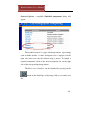
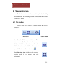
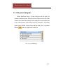
Bloch wave Simulator
User’s Manual
v. 1.0
Copyright © 2003-2009 AnaliteX
February 2009
Visit our web-page at: www.analitex.com
Bloch Simulator User’s Manual
Table of Contents
1
Preface ....................................................................................... 2-4
1.1
General introduction
2-4
1.2
Support offerings
2-4
1.3
Reporting problems
2-4
2
Installing Bloch wave Simulator ............................................... 2-5
2.1
Installation
2-5
2.2
User interface
2-5
3
Bloch Wave Simulator .............................................................. 3-7
3.1
Brief description of the Bloch wave theory
3-7
3.2
Speed of calculations
3-9
3.3
Limiting number of beams
3-10
3.4
Calculations type
3-12
4
Supported file formats ............................................................. 4-14
4.1
Native format XBLOCH
4-14
4.2
Crystallographic file types
4-15
5
The user interface .................................................................... 5-16
2-2
Bloch Simulator User’s Manual
5.1
The toolbar
5-16
5.2
Side panel dialog bar.
5-18
5.2.1
The Zone Axis and Tilt dialog panel .............................. 5-19
5.2.2
The Bloch Settings dialog panel ..................................... 5-20
5.2.3
The Thickness dialog panel ............................................ 5-22
5.3
Optimal Bloch settings
5-23
5.4
Colour control
5-24
6
Performing Bloch wave calculations ...................................... 6-25
7
Examples ................................................................................. 7-27
8
Suggested literature ................................................................. 8-31
2-3
Bloch Simulator User’s Manual
1 Preface
This preface provides information about the Bloch wave
Simulator User’s Manual and links to AnaliteX technical support.
1.1 General introduction
Bloch Simulator is a program which allows you to calculate and
visualize dynamical Convergent Beam Electron Diffraction (CBED)
patterns by the Bloch wave method.
1.2 Support offerings
You can always contact AnaliteX at [email protected]
find out how the Bloch wave Simulator program can meet your needs
and for technical support.
1.3 Reporting problems
If you can have problems while running Bloch wave Simulator
or any of its components, please report them to the AnaliteX support
team by email ([email protected]).
2-4
Bloch Simulator User’s Manual
2 Installing Bloch wave Simulator
Bloch wave Simulator runs under Windows® 2000, XP or Vista,
and is usually included as an optional component in the eMap
software package.
2.1 Installation
Install the program by clicking on Setup.exe located in the
directory eMap on the CD. The program will ask you to choose
destination location, the default is C:\Program Files\AnaliteX\eMap.
Use Browse if you want to put the program in another directory, or on
another drive. Click Next when the program folder and drive are as
required. Then you will be asked to select program folders under
which eMap is run from the Start menu. Select the program folder
(default = eMap) and click on Finish.
2.2 User interface
The Bloch wave Simulator module can be initiated from the
Start page. NOTE: This page will only appear if the MS Internet
Explorer is installed. In the case when eMap fails to locate the
2-5
Bloch Simulator User’s Manual
Internet Explorer, a simplified Installed components dialog will
appear.
The modules browser is a page with image buttons representing
each available module. A short description text is displayed on the
right side when you select the button using a mouse. To launch a
required component, click on the short description text on the right
side of the corresponding image button.
The Bloch wave Simulator can be launched by pressing on the
button on the Start Page or choosing a link to a recently used
file.
2-6
Bloch Simulator User’s Manual
3 Bloch Wave Simulator
The Bloch wave Simulator module is designed for the
calculation
and
visualization
of
Convergent
Beam
Electron
Diffraction (CBED) dynamical electron diffraction patterns.
The Bloch wave method:
•
conforms to calculations of diffraction patterns of
structures with small unit cell parameters;
•
is fast with high accuracy for a perfect crystal in a
<u,v,w> direction with low symmetry i.e. small number
of beams;
•
calculates CBED patterns in any <u,v,w> direction.
3.1 Brief description of the Bloch wave theory
The time-independent wave equation (Helmholtz equation or
elliptic partial differential equation) is:
where Ψ is the wave function, K0 is the relativistic wave number in the
form of 1/λ and
=
λ
with σ as the interaction constant and V(r) as the electrostatic (lattice)
potential.
3-7
Bloch Simulator User’s Manual
The lattice potential can be expanded into a Fourier series and
the electron wave inside the crystal for an arbitrary wave vector k can
be written as a Bloch wave,
Ψ = ∑ ,
where Cg are called Bloch wave coefficients.
Substituting Ψ(r) into the wave equation gives the following
form,
∑ − + + ∑ = 0,
or
− + + ∑ = 0.
This equation can be represented in a matrix form as followed,
− $ # #
⋮
# #
⋮
#
" &
− + ⋮
⋮
&
…
…
⋱
…
…
⋮
− + )
⋮
&
…
…
…
⋱
…
&
- $ &
, # ,
,# ⋮ ,
⋮
, = 0.
&
# ,
, ⋮
⋮
,# ,
− + * + "& +
The final problem can be solved using matrix diagonalization to
determine the wave vectors, k, and all the Bloch coefficients, Cg.
The Bloch wave Simulator uses an optimized diagonalization
functions from Intel® Math Kernel Library (Intel® MKL).
3-8
Bloch Simulator User’s Manual
3.2 Speed of calculations
The calculation speed depends on several parameters which are
described below.
Parameter
Description
gmax
Limits the total resolution of the simulated
diffraction pattern. Reflections with ghkl > gmax
will not be included in the calculations.
Sg,max
Maximum value for the excitation error, Sg.
Limits the number of exact beams.
Sg,Bethe
Maximum value for the excitation error, Sg.
Limits the number of Bethe beams.
HOLZ layers
Maximum number of HOLZ layers to include in
the calculations.
Voltage
At low voltages more HOLZ reflections can fall
within gmax.
Number of points
Every disk, line etc. will be digitized with
resolution equal to the specified number of
points. For example, in case of the CBED disk
the number of points Npoints corresponds to the
3-9
Bloch Simulator User’s Manual
CBED disk diameter. In this case the total
number of points inside every CBED disk would
be round(π·Npoints2).
NOTE: The total number of beams N produces a matrix of size
N*N with complex numbers of double precision as matrix elements.
With N=300, the memory requirements for the matrix storage will be
~1.4 Mb. The time needed to diagonalize a matrix with N=300 may
vary depending on the processor’s speed. For Intel® Core2 Quad this
time is less than 1 second per diagonalization. However, increasing
the number of beams can significantly increase the calculation time.
Note that in the case of a CBED disk the single matrix diagonalization
time will be multiplied by the number of pixels inside the disk. For
example a typical CBED pattern of a simple silicon crystal structure in
the [111] zone axis orientation with a CBED disk size of 16 pixels
would take about 20-30 sec to calculate on the Intel® Core2 Quad
processor.
3.3 Limiting number of beams
There are several options which can speed up the calculations,
especially in the case when the type of calculations is set to the CBED
disk with a large number of points.
3-10
Bloch Simulator User’s Manual
Figure. The geometry of the Bloch wave calculations
(see text for explanations).
Voltage. The curvature of the Ewald sphere increases with
lower accelerating voltage values (1Vacc < 2Vacc). Decreasing the
voltage can increase the total number of reflections, provided that
other parameters remain unchanged.
Sg,max. Increasing Sg,max will increase the number of reflections,
which will be counted as exact (blue area around the reciprocal layers
on Figure) and will participate in the matrix diagonalization.
Sg,Bethe. Increasing Sg,Bethe will increase the number of
reflections, which will be counted as Bethe (red area around the
reciprocal layers on Figure) and will participate only in Generalized
Bethe Approximation.
3-11
Bloch Simulator User’s Manual
Number of points. The total number of matrix diagonalizations
in the case of CBED disk calculation mode can be approximately
evaluated by the following equation:
./0/12 = 345678 ∙ .:0
;/< = ∙ .>?1&< .
where Nbeams is the total number of the exact beams in the diffraction
pattern. In the case of other calculation types the Ntotal will vary.
HOLZ layers. Changing the number of HOLZ layers will
increase the total number of reflections within the given gmax value.
3.4 Calculations type
There are several calculation types available in the Bloch wave
Simulator:
1.
Point. The dynamical diffraction pattern will be
calculated as a point (spot or regular) diffraction pattern.
2.
CBED disk. The dynamical diffraction pattern will be
calculated as a disk diffraction pattern.
3.
Rectangle. The dynamical diffraction pattern will be
calculated as a diffraction pattern with rectangular
reflections.
4.
Circle. The dynamical diffraction intensities will be
calculated only along every disk, forming circles with
3-12
Bloch Simulator User’s Manual
empty centres similar to a TEM DIFF mode with the
rocking beam on and without descan. The width (pixels)
of the circle stroke and circle radius (pixels) can be
specified in the Bloch Settings Panel.
5.
Precession. This calculation mode is similar to the
Circle mode except that after the calculations the
intensities will be averaged along the circle. The pattern
will be displayed as a regular dynamical spot precession
electron diffraction pattern similar to a TEM DIFF mode
with rocking beam on and with descan. The width
(pixels) of the circle stroke and circle radius (pixels) can
be specified in the Bloch Settings Panel
6.
LACBED. This calculation mode is similar to CBED
mode except only the 000 reflection will be shown.
7. Line. In this calculation mode a line segment of a CBED
disk will be calculated. The line slope (degrees), length
(pixels) and width (pixels) can be specified in the Bloch
Settings Panel.
3-13
Bloch Simulator User’s Manual
4 Supported file formats
Bloch wave Simulator supports several input data file types.
4.1 Native format XBLOCH
The native format of the Bloch wave Simulator is the XML file
format with custom file extension *.xbloch. The Bloch wave Simulator
will automatically generate files in this format and prompt for the
user’s permission to save before exit from the program.
The XBLOCH XML files contain the entire Bloch wave
Simulator settings and Bloch wave calculated data, if any calculations
were performed.
A XBLOCH file contains the complete crystallographic
information about the loaded crystal needed for Bloch wave
calculations. This crystallographic data includes:
•
the symmetry (space group number and extension);
•
the unit cell parameters;
•
information about unique atoms (chemical element name, xyz
fractional coordinates, occupancies and temperature factors).
4-14
Bloch Simulator User’s Manual
4.2 Crystallographic file types
The Bloch wave Simulator can load files which contain
crystallographic information such as symmetry, unit cell and atomic
positions. The file types are SHELX INS, CIF, XYZ, TXT (see the
eMap manual), AT and PDB.
4-15
Bloch Simulator User’s Manual
5 The user interface
The Bloch wave Simulator has several ways for data handling
and calculations. The following sections will describe the available
commands in details.
5.1 The toolbar
There is one extra toolbar available in the Bloch wave
Simulator:
Description
Toolbar button
Run. Starts the Bloch wave calculations. This
button can be disabled when the Bloch wave
Simulator finished the calculations or a file with
Bloch calculations was loaded. In order to restart
press the Create new document button (
).
Crystal structure view. Switches to the structure
preview mode (in the current zone axis
orientation).
5-16
Bloch Simulator User’s Manual
Diffraction pattern view. Switches to the
simulated diffraction pattern preview mode.
Colour control. Shows the colour control dialog
in
order
to
change
gamma/contrast/brightness
the
of
values
the
of
calculated
electron diffraction pattern.
5-17
Bloch Simulator User’s Manual
5.2 Side panel dialog bar.
Bloch Simulator offers a 3-panel dialog bar on the right side
(default) of the main view. This bar can be relocated to any side of the
current view or the main window (left or right sides are preferable due
to the vertical nature of the dialog bar items placement). Any dialog
panel can be hidden or closed any time by using the 2 respective
buttons
in the top-right corner of the bar.
The side panel Dialog bar
5-18
Bloch Simulator User’s Manual
5.2.1 The Zone Axis and Tilt dialog panel
The Zone Axis and Tilt dialog panel
allows the user to control the current
zone axis indices and the tilt away
from the zone axis (within values of
2D plane hk indices).
These controls may be disabled if the
Bloch data was calculated. In order to
The Zone Axis and Tilt dialog
reset the data and be able to modify
panel.
the zone axis and tilt press the Create
new document button (
).
5-19
Bloch Simulator User’s Manual
5.2.2 The Bloch Settings dialog panel
The Bloch Settings dialog panel allows
the user to control the current settings
for the Bloch wave calculations.
If the calculations type is Point then the
Number of points edit box will be set
to 1 and disabled automatically.
These controls may be disabled if the
Bloch data was calculated. In order to
reset the data and be able to modify
controls
press
document button (
the
Create
new
).
For the Line calculation mode the line
Width (in mrad) and the Slope (in
degrees) to the a-axis of the diffraction
pattern can be modified.
For the Circle and Precession modes
the Width (in mrad) of the ring can be
The Bloch Settings dialog panel.
modified.
5-20
Bloch Simulator User’s Manual
NOTE: Line specific settings. The Number of points has no
effect on the lined width and determines the sampling (resolution
along the line). The line width determined by the convergence angle –
it is a segment which is the result of the intersection of an infinite line
and the CBED disk.
The line slope related to the electron diffraction pattern axis, the line width and
length are marked.
5-21
Bloch Simulator User’s Manual
5.2.3 The Thickness dialog panel
The Thickness dialog panel allows the
user to control the current thickness
value, and to add and remove thickness
values to the list. The thickness list is
always enabled. Changing the selection
in the list will automatically change the
calculated
diffraction
dynamical
pattern.
The
electron
thickness
selection doesn’t affect the diffraction
pattern in preview mode (the mode with
blue circles representing the spots, see
The Thickness dialog panel.
next section).
5-22
Bloch Simulator User’s Manual
5.3 Optimal Bloch settings
Consider the following example. The electron diffraction pattern
of silicon along the [111] zone axis with current settings will be
displayed as:
Some overlapping of reflections is due to large values of Sg.
The optimal settings such as the beam convergence angle,
excitation error values Sg, maximum HOLZ number etc. can be
controlled visually in run-time via the side docking panels.
NOTE: The Sg value can be related to the kinematical crystal
thickness t and the kinematical extension of reflections in reciprocal
space as Sg = 1/t.
5-23
Bloch Simulator User’s Manual
.
The user can modify the numbers in the dialog boxes or change
them by dragging the corresponding scroll bars.
In the preview mode each blue circle corresponds to a CBED
disk. Some information (such as hkl, d and kinematical Fhkl values)
can be recalled by pointing the mouse to the centre of the
corresponding disk. The information will be shown in the bottomright corner.
5.4 Colour control
The following dialog will appear after pressing the colour
control button
.
5-24
Bloch Simulator User’s Manual
The user can modify the gamma, brightness and contrast values
of the calculated dynamical electron diffraction pattern in order to
increase the visual representation of some features on a diffraction
pattern.
It has affect only on the calculated electron diffraction pattern.
6 Performing Bloch wave calculations
In order to start the Bloch calculations press the Run button on
the Bloch wave Simulator toolbar. This button may be disabled if the
previous calculated Bloch data hasn’t been cleared or reset. In order to
reset the data and be able to run new calculations press the Create
new document button (
).
6-25
Bloch Simulator User’s Manual
When the calculations starts the following control dialog will
appear:
The calculations can be stopped at any time by pressing the Stop
button. Firstly the program will calculate the secular matrix while
informing the user about the current row been calculated.
After that the program will start the matrix diagonalization
procedure with the following dialog.
NOTE: the current time (in the first row) is exact, however the
estimated (total) time is only an approximation and may vary.
6-26
Bloch Simulator User’s Manual
7 Examples
The following dynamical electron diffraction patterns were
calculated by the Bloch method using the Bloch wave Simulator. The
conditions were:
Crystal: silicon;
Zone axis: [111]
Voltage: 200 kV
CBED disk size: 64 pixels
Convergence angle: 8 mrad
HOLZ included: 2
Thickness values: 100, 300, 500 and 1000 Å.
7-27
Bloch Simulator User’s Manual
100 Å
300 Å
7-28
Bloch Simulator User’s Manual
500 Å
1000 Å
7-29
Bloch Simulator User’s Manual
1000 Å, zoomed with FOLZ visible.
7-30
Bloch Simulator User’s Manual
8 Suggested literature
1. Z.L. Wang. Elastic and Inelastic Scattering in Electron Diffraction and
Imaging. Springer. 1995, 476 pp.
2. E.J. Kirkland. Advanced Computing in Electron Microscopy. Springer.
1998, 250 pp.
3. Marc De Graef. Introduction to Conventional Transmission Electron
Microscopy. Cambridge University Press. 2003, 718 pp.
4. L.-M. Peng, S.L. Dudarev, M.J. Whelan. High-Energy Electron
Diffraction and Microscopy. Oxford University Press. 2004, 536 pp.
8-31