1
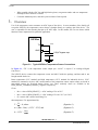
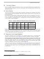
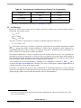
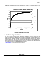
Freescale Semiconductor
Application Note
Using the 56F83xx
Temperature Sensor
Michael Stanley
1.
Contents
1. Introduction....................................... 1
2. Features and Benefits........................ 1
3. Overview........................................... 2
Introduction
The 56F83xx controllers developed by Freescale include an
on-chip temperature sensor. This module generates an output
voltage which is directly proportional to the internal junction
temperature of the device. Software running on the controller
can measure this voltage using the on-chip Analog-to-Digital
Converter (ADC), and that measured value can then be used to
calculate temperature.
2.
AN1980
Rev. 1, 9/2005
Features and Benefits
The 56F83xx temperature sensor offers these benefits:
•
Generates a temperature-dependent voltage over the
full temperature range specified for the device
•
Greater than 1 bit/degree C sensitivity at 10 bits of
resolution1
Room and/or hot temperature sensor trim values2 are
stored in on-chip non-volatile memory at the factory
Can be used for intelligent power control--powering
down portions of the system when temperatures near
specified maximums
Can be used as an input to temperature compensate
other portions of the system
Works in concert with the on-chip Analog-to-Digital
Converter (ADC)
•
•
•
•
1. The 56F83xx Analog-to-Digital Converters actually have 12
bits of resolution; therefore, the sensitivity can be restated to
be greater than 4 LSB/degree C.
2. Consult the Data Sheet for your specific device to determine
how it was trimmed at the factory.
© Freescale Semiconductor, Inc., 2005. All rights reserved.
4. Accuracy Issues ................................ 3
4.1 Sensor Linearity.................................. 3
4.2 Temperature Sensor Output
Impedance ........................................... 3
4.3 Random Noise .................................... 6
4.4 Trim Accuracy .................................... 6
4.5 Self-Heating ........................................ 7
5. Software Implementation............... 9
6. Conclusion ...................................10
7.References .....................................10
Overview
•
•
3.
When coupled with the ADC low and high limit registers, can generate under- and over-temperature
interrupts with no software overhead
Consumes minimum power, and can be powered down if not required
Overview
Use of the temperature sensor consumes an ADC input of the device. In most members of the family (all
except the 56F8322), the temperature sensor voltage is brought directly to a package pin of the device. The
user is responsible for then shorting that pin to an ADC input. In this manner, the user can choose which
function is more important to his particular application.
56F83xx
VTS
TS
ANA7
0.01µF bypass cap
Figure 3-1. Typical 56F83xx Temperature Sensor Connections
In Figure 3-1, “TS” is the temperature sensor output pin. “ANA7” is input #7 to Analog-to-Digital
Converter A.
The 56F8322 device connects the temperature sensor and ANA7 inside the package, and that node is not
brought outside the device.
Room temperature (25°C nominal) and high temperature (125°C nominal for industrial devices; 150°C
nominal for automotive devices) ADC measurements of the temperature sensor output voltage are stored in
non-volatile storage by Freescale during factory test. These read-only values are available in the
HFM_IFROPT_2 and HFM_IFROPT_0 registers, respectively.
Given:
•
RRT = value of HFM_IFROPT_2 = ADC reading of VTS at 25°C
•
RHT = value of HFM_IFROPT_0 = ADC reading of VTS at 125°C (or 150°C)
•
R = current ADC result of measuring VTS
then temperature T is approximated by:
R
+ b , where:
m
m = (RHT - RRT) / (125°C - 25°C) and
R
b = 125°C - HT
m
T=
(Equation 1)
(Equation 2)
(Equation 3)
56F8300 ADC, Rev. 1
2
Freescale Semiconductor
Temperature Sensor Output Impedance
4.
Accuracy Issues
There are a number of factors which affect the accuracy of measurements made using the temperature sensor.
These include inherent limitations of the device, trim accuracy and board impacts, and are discussed in the
following subsections.
4.1 Sensor Linearity
There are two major blocks involved in taking a temperature measurement: the temperature sensor block,
which generates the temperature-dependent voltage and the Analog-to-Digital Converter, which converts the
value into digital form.
In a recent set of lab measurements, the analog output voltage of the sensor was oversampled (by 10x) at 25°C,
125°C, 135°C and 150°C for a number of devices. The averages of each of those temperatures was used to
extract an equation for each individual device1. The standard error of estimate about those lines ranged from
2.6mV to 8.3mV, as shown in Table 4-1.
Table 4-1. Variance in Measured Temperature Sensor Analog Voltage
VRT
(25°C)
VHT
(135°C)
Average
s (V/C)
k (V)
Standard Error of
Estimate (V)
0.00746
1.429
0.0046
Minimum
1.576
2.40
0.00729
1.387
0.0026
Maximum
1.684
2.50
0.00769
1.498
0.0083
Table 4-1 dealt with the temperature sensor voltage as measured by an external monitor. In practice, the
on-chip ADC will be used to perform this conversion. The 56F83xx family’s ADCs are expected to operate
with an effective number of bits (ENOB) of 9 or 10. Assuming 3.3V full range for the ADC, this equates to
+/-3.2 to 6.4mV accuracy for the ADC conversion itself.
4.2 Temperature Sensor Output Impedance
The 56F83xx temperature sensor was designed to use a minimum amount of power. A fairly high output
impedance was the design trade-off made. Figure 4-1 illustrates the limited drive capability of this module.
The typical application externally connects the temperature sensor output to an ADC input. The 56F83xx ADC
has a switched capacitor sample-and-hold circuit in its input stage. When this switch closes (at the rising edge
of the ADC's sample clock), there can be an instantaneous current, required to charge up the sampling
capacitor. Though this capacitor is quite small, the high output impedance of the temperature sensor's output
can result in a disturbance of the node's voltage, as shown in Figure 4-2.
Adding a 0.01µF bypass capacitor to the temperature sensor output/ADC input node effectively mitigates this
error source. However, if the ADC is used to sample the node continuously and at a high-enough frequency,
the temperature sensor output will see a low load impedance and this source of measurement error will
re-manifest itself.
1. V= (s * T) + k, where “s” is in volts/degree C, “T” is in degrees C and “k” is in volts
56F8300 ADC, Rev. 1
Freescale Semiconductor
3
Accuracy Issues
"Temperature Sense Pin IV Curve"
50
40
uA
30
20
10
0
-10
1
1.5
2
2.5
3
3.5
4
Volts
Figure 4-1. Temperature Sensor Output I/V Curve
Figure 4-2. Temperature Sensor Output Droop
56F8300 ADC, Rev. 1
4
Freescale Semiconductor
Temperature Sensor Output Impedance
The workaround has four components:
•
Add a 0.01µF capacitor to the sensor output/ADC input node
•
Limit the time between ADC samples on this node to greater than or equal to 1µs
•
Allow at least 10ms after powering up the temperature sensor before initiating any measurements,
which allows the temperature sensor time to charge up the bypass capacitor
•
Program the ADC so that the channel assigned to the temperature sensor is never the last to be
measured in any given measurement sequence1
These steps effectively remove any effects of the sensor output impedance from the measurement.
However, an issue still exists for the 56F8322, in which the sensor output is not brought to a package pin. In
this case, there are two alternatives:
•
Live with the decreased accuracy. Characterizations are not complete at the time of this writing, but
measurements made on an early 56F8345 device (with no bypass capacitor on the temperature sensor
output) indicates that the standard error of estimate for the converted voltage may increase to 60mV or
more.
•
Lower the ADC clock rate so that the sample/hold circuit closes after the sensor has recharged the
internal switched cap circuits, effectively bypassing the “droop”. Decreasing the ADC clock rate to
125KHz or slower should take care of this problem.
1. During some modes of operation, the 56F83xx ADC sample & hold circuit will continuously sample the
last input(s) listed in the ADC Channel List registers between sample periods. For this reason, the channel assigned for use in sampling the temperature sensor voltage should never be the last channel sampled.
56F8300 ADC, Rev. 1
Freescale Semiconductor
5
Accuracy Issues
4.3 Random Noise
56F8357 Temp Sensor Voltage
Histogram of "RT under power" measurements (5000)
600
Frequency
500
Maximum = 1.948096
Mean = 1.938688
Minimum = 1.925537
StdDev = 0.002976
Max - Min = 0.0226
400
300
200
100
1.947
1.945
1.943
1.941
1.939
1.937
1.935
1.933
1.931
1.929
1.927
1.926
0
TS Voltage as Measured by the ADC
Figure 4-3. Temperature Sensor Voltage as Measured by the ADC
The printed circuit board layout must be considered in any system that performs Analog-to-Digital
conversions, as short traces and clean analog supplies are essential for accurate results. Additionally, since
temperature will be changing extremely slowly compared with virtually any other system input, it can be
oversampled to filter out much of the random noise.
Figure 4-3 summarizes 5,000 temperature sensor measurements that were taken of a device on a socketed
board. The device was first allowed to run at speed for 20 minutes in order to reach thermal equilibrium before
the measurements were taken. Note that the spread of measured values is approximately 23mV, which
corresponds to about 3°C.
Finally, the value of the DIV field in ADCR2 controls the frequency of the ADC internal clock versus the
master system/peripheral clock. The amount of noise showing up on ADC measurements can often be reduced
by slight changes in the value of this prescaler. The device shown Figure 4-3 was running with a DIV value of
7 under nominal conditions with a 0.0047µF bypass capacitor on TS (The recommended bypass capacitor
value is 0.01µF).
4.4 Trim Accuracy
Specifications for TRT and THT are shown in Table 4-2. This variance must obviously be factored into the final
calculated value for T.
56F8300 ADC, Rev. 1
6
Freescale Semiconductor
Self-Heating
Table 4-2. Environmental Conditions During Factory Trim Programming
Temperature
Nominal Value
Variance
TRT
26°C
+/- 2°C
THT (Industrial)
125°C
+/- 3°C
THT (Automotive)
150°C
+/- 3°C
Trim accuracy is also limited by self-heating. See Section 4.5 for details.
4.5 Self-Heating
Because the 56F83xx devices draw non-zero supply current, they consume power and are therefore subject to
self-heating. For example, assume:
VDD = 3.3V
IDD = 120mA
ThetaJA = 40°C/W
The device can then be expected to have a junction-to-ambient temperature difference of:
3.3 x .12 x 40 = 16°C
IDD is a function of device type, frequency of operation, code being executed, number of peripherals enabled
and VDD, among other things. Accurate estimation of 56F83xx power dissipation will be addressed in a
separate application note. Likewise, ThetaJA is a function of the device, package, heat sink, board design, TA
and TJ. See the device Data Sheet for further information.
One question which arises is “Just how fast does the device self-heat after power-up?”. An experiment was
performed in an effort to answer this. A 56F83xx device was placed in a low-power Stop mode assumed to
have minimal self-heating and allowed some time to reach thermal equilibrium. The mode was then switched
to Run at 60MHz, and the temperature sensor sampled at regular intervals.1
These readings can be used with Equations (1) through (3) (See Section 3.) to calculate Tj. Both VTS and Tj
are shown in Figure 4-4 and Figure 4-5. The data is the same for both figures, although Figure 4-4 has an
expanded time scale to focus on the initial seconds.
From these, it is apparent that the device has an initial burst of self-heating, followed by a slower ramp rate
upward. It seems logical to assume that the first represents the period at which the device is primarily heating
just the package, and the second is when heat transfer to the PC board dominates.
1. Node TS was not bypassed on the bench used for these measurements. This can account for some of the
noise seen in the figures.
56F8300 ADC, Rev. 1
Freescale Semiconductor
7
Accuracy Issues
Temperature Sensor Voltage Versus Time
1.82
25
20
1.78
Volts
1.76
15
1.74
1.72
10
1.7
1.68
5
Approximate change in
temperature (C)
1.8
1.66
1.64
0
0
10
20
seconds
30
40
Figure 4-4. Estimated Tj Over Time (A)
Because each device/board combination will vary, it is important not to focus too closely on the specific
numbers shown. The point to be taken is that, given time, the device Tj will rise significantly above ambient
temperature. Time to thermal equilibrium is measured in minutes, although the initial burst of self-heating
occurs in only a few seconds.
Because of this characteristic, Freescale measures trim values for the temperature sensor very early in the
production test sequence, before the bulk of self-heating has occurred. The trim values are typically completed
during the first 20ms after the device is powered up.
56F8300 ADC, Rev. 1
8
Freescale Semiconductor
Self-Heating
Additionally, it is important to note that the temperature sensor measures Tj of the 56F83xx devices. It does
NOT measure the ambient temperature.
Temperature Sensor Voltage Versus Time
1.82
25
1.8
Volts
1.76
15
1.74
1.72
10
1.7
1.68
Approximate change in
temperature (C)
20
1.78
5
1.66
1.64
0
100
200
seconds
300
0
400
Figure 4-5. Estimated Tj Over Time (B)
5.
Software Implementation
The 56F83xx Analog-to-Digital Converter implementation has numerous modes of operation. All these
features are available to code which implements temperature-sensing functions. For instance, the ADC can be
set to continuously sample the temperature sensor voltage at some frequency, comparing each conversion
result with either the ADC high or low limit registers. Exceeding either one or both values could then result in
an interrupt service routine being called. Thus, either an under- or over-temperature alarm can be implemented
with essentially zero software overhead on the main processing loop.
Code Example 5-1 illustrates the steps required to measure Tj.
56F8300 ADC, Rev. 1
Freescale Semiconductor
9
Conclusion
Code Example 5-1. Steps Required to Measure Tj
#define TSENSOR_CONTROL 0x00F270
#define ADCA_POWER 0x00F229
#define ADCB_POWER 0x00F269
#define HFM_IFROPT_2 0x00F41C
#define HFM_IFROPT_0 0x00F41A
#define ADCA_ADCR1 0x00F200
#define ADCA_ADLST1 0x00F203
#define ADCA_ADSDIS 0x00F205
#define ADCA_ADSTAT 0x00F206
#define ADCA_ADRSLT0 0x00F209
0x0001 => TSENSOR_CONTROL # enable temp sensor
0x00D0 => ADCA_POWER # turn on ADC A
rrt <= HFM_IFROPT_2 # Room temperature trim value
rht <= HFM_IFROPT_0 # Hot temperature trim value
m = (150 - 25)/(rht - rrt) # slope of the T vs ADC result curve
b = 150 - m * rht
# the y-intercept
0x0004 => ADCA_ADCR1 # Triggered Sequential
0x7707 => ADCA_ADLST1 # ADLST1 set to sample ANA7
0x00FC => ADCA_ADSDIS # enable only sample1 0 and 1
# allow sufficient time for ADC reference and temperature
# sensor circuits to power up (25msec recommended).
0x2004 => ADCR1
# ADCR1 - initiate the conversion
status = 0
# wait for the conversion to complete
while (status not equal to 0x0803) status <= ADSTAT
adc_result <= ADCA_ADRSLT0
temperature = m * adc_result + b
Notes: It is best to oversample and filter (not shown).
6.
Conclusion
The 56F83xx temperature sensor module provides a convenient and inexpensive way to adjust for temperature
variances and restrictions. The results obtained are subject to a number of limitations, and proper system
design based on the issues discussed in this application note can significantly increase its accuracy.
7.
References
1. 56F8300 Peripheral User Manual, MC56F8300UM
2. 56F83xx Technical Data document specific to the device you’re implementing, MC56F83xx
3. DSP56800E Reference Manual, DSP56800ERM
56F8300 ADC, Rev. 1
10
Freescale Semiconductor
Self-Heating
56F8300 ADC, Rev. 1
Freescale Semiconductor
11
How to Reach Us:
Home Page:
www.freescale.com
E-mail:
[email protected]
USA/Europe or Locations Not Listed:
Freescale Semiconductor
Technical Information Center, CH370
1300 N. Alma School Road
Chandler, Arizona 85224
+1-800-521-6274 or +1-480-768-2130
[email protected]
Europe, Middle East, and Africa:
Freescale Halbleiter Deutschland GmbH
Technical Information Center
Schatzbogen 7
81829 Muenchen, Germany
+44 1296 380 456 (English)
+46 8 52200080 (English)
+49 89 92103 559 (German)
+33 1 69 35 48 48 (French)
[email protected]
Japan:
Freescale Semiconductor Japan Ltd.
Headquarters
ARCO Tower 15F
1-8-1, Shimo-Meguro, Meguro-ku,
Tokyo 153-0064, Japan
0120 191014 or +81 3 5437 9125
[email protected]
Asia/Pacific:
Freescale Semiconductor Hong Kong Ltd.
Technical Information Center
2 Dai King Street
Tai Po Industrial Estate
Tai Po, N.T., Hong Kong
+800 2666 8080
[email protected]
For Literature Requests Only:
Freescale Semiconductor Literature Distribution Center
P.O. Box 5405
Denver, Colorado 80217
1-800-441-2447 or 303-675-2140
Fax: 303-675-2150
[email protected]
Information in this document is provided solely to enable system and
software implementers to use Freescale Semiconductor products. There are
no express or implied copyright licenses granted hereunder to design or
fabricate any integrated circuits or integrated circuits based on the
information in this document.
Freescale Semiconductor reserves the right to make changes without further
notice to any products herein. Freescale Semiconductor makes no warranty,
representation or guarantee regarding the suitability of its products for any
particular purpose, nor does Freescale Semiconductor assume any liability
arising out of the application or use of any product or circuit, and specifically
disclaims any and all liability, including without limitation consequential or
incidental damages. “Typical” parameters that may be provided in Freescale
Semiconductor data sheets and/or specifications can and do vary in different
applications and actual performance may vary over time. All operating
parameters, including “Typicals”, must be validated for each customer
application by customer’s technical experts. Freescale Semiconductor does
not convey any license under its patent rights nor the rights of others.
Freescale Semiconductor products are not designed, intended, or authorized
for use as components in systems intended for surgical implant into the body,
or other applications intended to support or sustain life, or for any other
application in which the failure of the Freescale Semiconductor product could
create a situation where personal injury or death may occur. Should Buyer
purchase or use Freescale Semiconductor products for any such unintended
or unauthorized application, Buyer shall indemnify and hold Freescale
Semiconductor and its officers, employees, subsidiaries, affiliates, and
distributors harmless against all claims, costs, damages, and expenses, and
reasonable attorney fees arising out of, directly or indirectly, any claim of
personal injury or death associated with such unintended or unauthorized
use, even if such claim alleges that Freescale Semiconductor was negligent
regarding the design or manufacture of the part.
Freescale™ and the Freescale logo are trademarks of Freescale Semiconductor,
Inc. All other product or service names are the property of their respective owners.
This product incorporates SuperFlash® technology licensed from SST.
© Freescale Semiconductor, Inc. 2005. All rights reserved.
AN1980
Rev. 1
9/2005