1
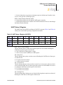
High-Performance 8-Bit Microcontrollers
Z8 Encore! XP® F082A
Series
Product Specification
PS022825-0908
Copyright ©2008 by Zilog®, Inc. All rights reserved.
www.zilog.com
Warning: DO NOT USE IN LIFE SUPPORT
LIFE SUPPORT POLICY
ZILOG'S PRODUCTS ARE NOT AUTHORIZED FOR USE AS CRITICAL COMPONENTS IN LIFE
SUPPORT DEVICES OR SYSTEMS WITHOUT THE EXPRESS PRIOR WRITTEN APPROVAL OF
THE PRESIDENT AND GENERAL COUNSEL OF ZILOG CORPORATION.
As used herein
Life support devices or systems are devices which (a) are intended for surgical implant into the body, or (b)
support or sustain life and whose failure to perform when properly used in accordance with instructions for
use provided in the labeling can be reasonably expected to result in a significant injury to the user. A
critical component is any component in a life support device or system whose failure to perform can be
reasonably expected to cause the failure of the life support device or system or to affect its safety or
effectiveness.
Document Disclaimer
©2008 by Zilog, Inc. All rights reserved. Information in this publication concerning the devices,
applications, or technology described is intended to suggest possible uses and may be superseded. ZILOG,
INC. DOES NOT ASSUME LIABILITY FOR OR PROVIDE A REPRESENTATION OF ACCURACY
OF THE INFORMATION, DEVICES, OR TECHNOLOGY DESCRIBED IN THIS DOCUMENT.
Z I L O G A L S O D O E S N O T A S S U M E L I A B I L I T Y F O R I N T E L L E C T U A L P R O P E RT Y
INFRINGEMENT RELATED IN ANY MANNER TO USE OF INFORMATION, DEVICES, OR
TECHNOLOGY DESCRIBED HEREIN OR OTHERWISE. The information contained within this
document has been verified according to the general principles of electrical and mechanical engineering.
Z8, Z8 Encore!, and Z8 Encore! XP are registered trademarks of Zilog, Inc. All other product or service
names are the property of their respective owners.
PS022825-0908
Z8 Encore! XP® F082A Series
Product Specification
iii
Revision History
Each instance in Revision History reflects a change to this document from its previous
revision. For more details, refer to the corresponding pages and appropriate links in the
table below.
Date
PS022825-0908
Revision
Level
Description
Page Number
September
2008
25
Added the references to F042A series back 3, 9, 16, 19, 37,
251
in Table 1, Available Packages, Table 5,
Table 7, Table 13, Ordering Information
sections.
May 2008
24
Changed title to Z8 Encore! XP F082A
Series and removed references to F042A
series in Table 1, Available Packages,
Table 5, Table 7, Table 13, Ordering
Information sections.
All
December
2007
23
Updated Figure 3, Table 14, Table 58
through Table 60.
10, 41, and 95
July 2007
22
Updated Table 15 and Table 128. Updated 44, 221
Power consumption in Electrical
Characteristics chapter.
June 2007
21
Revision number update.
All
Revision History
Z8 Encore! XP® F082A Series
Product Specification
iv
Table of Contents
Overview . . . . . . . . . . . . . . . . . . . . . . . . . . . . . . . . . . . . . . . . . . . . . . . . . . . . . . 1
Features . . . . . . . . . . . . . . . . . . . . . . . . . . . . . . . . . . . . . . . . . . . . . . . . . . . . . . .
Part Selection Guide . . . . . . . . . . . . . . . . . . . . . . . . . . . . . . . . . . . . . . . . . . . . . .
Block Diagram . . . . . . . . . . . . . . . . . . . . . . . . . . . . . . . . . . . . . . . . . . . . . . . . . . .
CPU and Peripheral Overview . . . . . . . . . . . . . . . . . . . . . . . . . . . . . . . . . . . . . .
eZ8 CPU Features . . . . . . . . . . . . . . . . . . . . . . . . . . . . . . . . . . . . . . . . . . . .
10-Bit Analog-to-Digital Converter . . . . . . . . . . . . . . . . . . . . . . . . . . . . . . . . .
Low-Power Operational Amplifier . . . . . . . . . . . . . . . . . . . . . . . . . . . . . . . . .
Internal Precision Oscillator . . . . . . . . . . . . . . . . . . . . . . . . . . . . . . . . . . . . . .
Temperature Sensor . . . . . . . . . . . . . . . . . . . . . . . . . . . . . . . . . . . . . . . . . . .
Analog Comparator . . . . . . . . . . . . . . . . . . . . . . . . . . . . . . . . . . . . . . . . . . . .
External Crystal Oscillator . . . . . . . . . . . . . . . . . . . . . . . . . . . . . . . . . . . . . . .
Low Voltage Detector . . . . . . . . . . . . . . . . . . . . . . . . . . . . . . . . . . . . . . . . . .
On-Chip Debugger . . . . . . . . . . . . . . . . . . . . . . . . . . . . . . . . . . . . . . . . . . . .
Universal Asynchronous Receiver/Transmitter . . . . . . . . . . . . . . . . . . . . . . .
Timers . . . . . . . . . . . . . . . . . . . . . . . . . . . . . . . . . . . . . . . . . . . . . . . . . . . . . .
General-Purpose Input/Output . . . . . . . . . . . . . . . . . . . . . . . . . . . . . . . . . . .
Direct LED Drive . . . . . . . . . . . . . . . . . . . . . . . . . . . . . . . . . . . . . . . . . . . . . .
Flash Controller . . . . . . . . . . . . . . . . . . . . . . . . . . . . . . . . . . . . . . . . . . . . . . .
Non-Volatile Data Storage . . . . . . . . . . . . . . . . . . . . . . . . . . . . . . . . . . . . . . .
Interrupt Controller . . . . . . . . . . . . . . . . . . . . . . . . . . . . . . . . . . . . . . . . . . . .
Reset Controller . . . . . . . . . . . . . . . . . . . . . . . . . . . . . . . . . . . . . . . . . . . . . .
1
2
4
5
5
5
6
6
6
6
6
6
6
7
7
7
7
7
7
8
8
Pin Description . . . . . . . . . . . . . . . . . . . . . . . . . . . . . . . . . . . . . . . . . . . . . . . . . 9
Available Packages . . . . . . . . . . . . . . . . . . . . . . . . . . . . . . . . . . . . . . . . . . . . . . . 9
Pin Configurations . . . . . . . . . . . . . . . . . . . . . . . . . . . . . . . . . . . . . . . . . . . . . . . . 9
Signal Descriptions . . . . . . . . . . . . . . . . . . . . . . . . . . . . . . . . . . . . . . . . . . . . . . 11
Pin Characteristics . . . . . . . . . . . . . . . . . . . . . . . . . . . . . . . . . . . . . . . . . . . . . . 13
Address Space . . . . . . . . . . . . . . . . . . . . . . . . . . . . . . . . . . . . . . . . . . . . . . . . 15
Register File . . . . . . . . . . . . . . . . . . . . . . . . . . . . . . . . . . . . . . . . . . . . . . . . . . .
Program Memory . . . . . . . . . . . . . . . . . . . . . . . . . . . . . . . . . . . . . . . . . . . . . . . .
Data Memory . . . . . . . . . . . . . . . . . . . . . . . . . . . . . . . . . . . . . . . . . . . . . . . . . . .
Flash Information Area . . . . . . . . . . . . . . . . . . . . . . . . . . . . . . . . . . . . . . . . . . .
15
15
17
17
Register Map . . . . . . . . . . . . . . . . . . . . . . . . . . . . . . . . . . . . . . . . . . . . . . . . . . 19
PS022825-0908
Table of Contents
Z8 Encore! XP® F082A Series
Product Specification
v
Reset, Stop Mode Recovery, and Low Voltage Detection . . . . . . . . . . . . . . 23
Reset Types . . . . . . . . . . . . . . . . . . . . . . . . . . . . . . . . . . . . . . . . . . . . . . . . . . .
Reset Sources . . . . . . . . . . . . . . . . . . . . . . . . . . . . . . . . . . . . . . . . . . . . . . . . . .
Power-On Reset . . . . . . . . . . . . . . . . . . . . . . . . . . . . . . . . . . . . . . . . . . . . .
Voltage Brownout Reset . . . . . . . . . . . . . . . . . . . . . . . . . . . . . . . . . . . . . . .
Watchdog Timer Reset . . . . . . . . . . . . . . . . . . . . . . . . . . . . . . . . . . . . . . . .
External Reset Input . . . . . . . . . . . . . . . . . . . . . . . . . . . . . . . . . . . . . . . . . .
External Reset Indicator . . . . . . . . . . . . . . . . . . . . . . . . . . . . . . . . . . . . . . .
On-Chip Debugger Initiated Reset . . . . . . . . . . . . . . . . . . . . . . . . . . . . . . .
Stop Mode Recovery . . . . . . . . . . . . . . . . . . . . . . . . . . . . . . . . . . . . . . . . . . . . .
Stop Mode Recovery Using Watchdog Timer Time-Out . . . . . . . . . . . . . . .
Stop Mode Recovery Using a GPIO Port Pin Transition . . . . . . . . . . . . . . .
Stop Mode Recovery Using the External RESET Pin . . . . . . . . . . . . . . . . .
Low Voltage Detection . . . . . . . . . . . . . . . . . . . . . . . . . . . . . . . . . . . . . . . . . . .
Reset Register Definitions . . . . . . . . . . . . . . . . . . . . . . . . . . . . . . . . . . . . . . . . .
23
25
25
26
27
27
28
28
28
29
29
30
30
30
Low-Power Modes . . . . . . . . . . . . . . . . . . . . . . . . . . . . . . . . . . . . . . . . . . . . . . 33
STOP Mode . . . . . . . . . . . . . . . . . . . . . . . . . . . . . . . . . . . . . . . . . . . . . . . . . . . .
HALT Mode . . . . . . . . . . . . . . . . . . . . . . . . . . . . . . . . . . . . . . . . . . . . . . . . . . . .
Peripheral-Level Power Control . . . . . . . . . . . . . . . . . . . . . . . . . . . . . . . . . . . .
Power Control Register Definitions . . . . . . . . . . . . . . . . . . . . . . . . . . . . . . . . . .
33
34
34
34
General-Purpose Input/Output . . . . . . . . . . . . . . . . . . . . . . . . . . . . . . . . . . . . 37
GPIO Port Availability By Device . . . . . . . . . . . . . . . . . . . . . . . . . . . . . . . . . . . .
Architecture . . . . . . . . . . . . . . . . . . . . . . . . . . . . . . . . . . . . . . . . . . . . . . . . . . . .
GPIO Alternate Functions . . . . . . . . . . . . . . . . . . . . . . . . . . . . . . . . . . . . . . . . .
Direct LED Drive . . . . . . . . . . . . . . . . . . . . . . . . . . . . . . . . . . . . . . . . . . . . . . . .
Shared Reset Pin . . . . . . . . . . . . . . . . . . . . . . . . . . . . . . . . . . . . . . . . . . . . . . .
Shared Debug Pin . . . . . . . . . . . . . . . . . . . . . . . . . . . . . . . . . . . . . . . . . . . . . . .
Crystal Oscillator Override . . . . . . . . . . . . . . . . . . . . . . . . . . . . . . . . . . . . . . . .
5 V Tolerance . . . . . . . . . . . . . . . . . . . . . . . . . . . . . . . . . . . . . . . . . . . . . . . . . .
External Clock Setup . . . . . . . . . . . . . . . . . . . . . . . . . . . . . . . . . . . . . . . . . . . . .
GPIO Interrupts . . . . . . . . . . . . . . . . . . . . . . . . . . . . . . . . . . . . . . . . . . . . . . . . .
GPIO Control Register Definitions . . . . . . . . . . . . . . . . . . . . . . . . . . . . . . . . . . .
Port A–D Address Registers . . . . . . . . . . . . . . . . . . . . . . . . . . . . . . . . . . . .
Port A–D Control Registers . . . . . . . . . . . . . . . . . . . . . . . . . . . . . . . . . . . . .
Port A–D Data Direction Sub-Registers . . . . . . . . . . . . . . . . . . . . . . . . . . .
Port A–D Alternate Function Sub-Registers . . . . . . . . . . . . . . . . . . . . . . . .
PS022825-0908
37
38
38
39
39
39
40
40
40
45
45
46
46
47
47
Table of Contents
Z8 Encore! XP® F082A Series
Product Specification
vi
Port A–C Input Data Registers . . . . . . . . . . . . . . . . . . . . . . . . . . . . . . . . . .
Port A–D Output Data Register . . . . . . . . . . . . . . . . . . . . . . . . . . . . . . . . . .
LED Drive Enable Register . . . . . . . . . . . . . . . . . . . . . . . . . . . . . . . . . . . . .
LED Drive Level High Register. . . . . . . . . . . . . . . . . . . . . . . . . . . . . . . . . . .
LED Drive Level Low Register . . . . . . . . . . . . . . . . . . . . . . . . . . . . . . . . . . .
51
52
52
53
53
Interrupt Controller . . . . . . . . . . . . . . . . . . . . . . . . . . . . . . . . . . . . . . . . . . . . . 55
Interrupt Vector Listing . . . . . . . . . . . . . . . . . . . . . . . . . . . . . . . . . . . . . . . . . . .
Architecture . . . . . . . . . . . . . . . . . . . . . . . . . . . . . . . . . . . . . . . . . . . . . . . . . . . .
Operation . . . . . . . . . . . . . . . . . . . . . . . . . . . . . . . . . . . . . . . . . . . . . . . . . . . . . .
Master Interrupt Enable . . . . . . . . . . . . . . . . . . . . . . . . . . . . . . . . . . . . . . . .
Interrupt Vectors and Priority . . . . . . . . . . . . . . . . . . . . . . . . . . . . . . . . . . . .
Interrupt Assertion . . . . . . . . . . . . . . . . . . . . . . . . . . . . . . . . . . . . . . . . . . . .
Software Interrupt Assertion . . . . . . . . . . . . . . . . . . . . . . . . . . . . . . . . . . . .
Watchdog Timer Interrupt Assertion . . . . . . . . . . . . . . . . . . . . . . . . . . . . . .
Interrupt Control Register Definitions . . . . . . . . . . . . . . . . . . . . . . . . . . . . . . . .
Interrupt Request 0 Register . . . . . . . . . . . . . . . . . . . . . . . . . . . . . . . . . . . .
Interrupt Request 1 Register . . . . . . . . . . . . . . . . . . . . . . . . . . . . . . . . . . . .
Interrupt Request 2 Register . . . . . . . . . . . . . . . . . . . . . . . . . . . . . . . . . . . .
IRQ0 Enable High and Low Bit Registers . . . . . . . . . . . . . . . . . . . . . . . . . .
IRQ1 Enable High and Low Bit Registers . . . . . . . . . . . . . . . . . . . . . . . . . .
IRQ2 Enable High and Low Bit Registers . . . . . . . . . . . . . . . . . . . . . . . . . .
Interrupt Edge Select Register . . . . . . . . . . . . . . . . . . . . . . . . . . . . . . . . . .
Shared Interrupt Select Register . . . . . . . . . . . . . . . . . . . . . . . . . . . . . . . . .
Interrupt Control Register . . . . . . . . . . . . . . . . . . . . . . . . . . . . . . . . . . . . . .
55
57
57
57
58
58
59
59
60
60
61
62
62
63
65
66
66
67
Timers . . . . . . . . . . . . . . . . . . . . . . . . . . . . . . . . . . . . . . . . . . . . . . . . . . . . . . . . 69
Architecture . . . . . . . . . . . . . . . . . . . . . . . . . . . . . . . . . . . . . . . . . . . . . . . . . . . .
Operation . . . . . . . . . . . . . . . . . . . . . . . . . . . . . . . . . . . . . . . . . . . . . . . . . . . . . .
Timer Operating Modes . . . . . . . . . . . . . . . . . . . . . . . . . . . . . . . . . . . . . . . .
Reading the Timer Count Values . . . . . . . . . . . . . . . . . . . . . . . . . . . . . . . .
Timer Pin Signal Operation . . . . . . . . . . . . . . . . . . . . . . . . . . . . . . . . . . . . .
Timer Control Register Definitions . . . . . . . . . . . . . . . . . . . . . . . . . . . . . . . . . .
Timer 0–1 Control Registers . . . . . . . . . . . . . . . . . . . . . . . . . . . . . . . . . . . .
Timer 0–1 High and Low Byte Registers . . . . . . . . . . . . . . . . . . . . . . . . . . .
Timer Reload High and Low Byte Registers . . . . . . . . . . . . . . . . . . . . . . . .
Timer 0-1 PWM High and Low Byte Registers . . . . . . . . . . . . . . . . . . . . . .
69
70
70
82
82
83
83
87
87
88
Watchdog Timer . . . . . . . . . . . . . . . . . . . . . . . . . . . . . . . . . . . . . . . . . . . . . . . 91
Operation . . . . . . . . . . . . . . . . . . . . . . . . . . . . . . . . . . . . . . . . . . . . . . . . . . . . . . 91
Watchdog Timer Refresh . . . . . . . . . . . . . . . . . . . . . . . . . . . . . . . . . . . . . . 92
PS022825-0908
Table of Contents
Z8 Encore! XP® F082A Series
Product Specification
vii
Watchdog Timer Time-Out Response . . . . . . . . . . . . . . . . . . . . . . . . . . . . .
Watchdog Timer Reload Unlock Sequence . . . . . . . . . . . . . . . . . . . . . . . .
Watchdog Timer Calibration . . . . . . . . . . . . . . . . . . . . . . . . . . . . . . . . . . . . . . .
Watchdog Timer Control Register Definitions . . . . . . . . . . . . . . . . . . . . . . . . . .
Watchdog Timer Control Register . . . . . . . . . . . . . . . . . . . . . . . . . . . . . . . .
Watchdog Timer Reload Upper, High and Low Byte Registers . . . . . . . . . .
92
93
93
94
94
94
Universal Asynchronous Receiver/Transmitter . . . . . . . . . . . . . . . . . . . . . . 97
Architecture . . . . . . . . . . . . . . . . . . . . . . . . . . . . . . . . . . . . . . . . . . . . . . . . . . . . 97
Operation . . . . . . . . . . . . . . . . . . . . . . . . . . . . . . . . . . . . . . . . . . . . . . . . . . . . . . 98
Data Format . . . . . . . . . . . . . . . . . . . . . . . . . . . . . . . . . . . . . . . . . . . . . . . . 98
Transmitting Data using the Polled Method . . . . . . . . . . . . . . . . . . . . . . . . 99
Transmitting Data using the Interrupt-Driven Method . . . . . . . . . . . . . . . . 100
Receiving Data using the Polled Method . . . . . . . . . . . . . . . . . . . . . . . . . 101
Receiving Data using the Interrupt-Driven Method . . . . . . . . . . . . . . . . . . 102
Clear To Send (CTS) Operation . . . . . . . . . . . . . . . . . . . . . . . . . . . . . . . . 103
MULTIPROCESSOR (9-bit) Mode . . . . . . . . . . . . . . . . . . . . . . . . . . . . . . 103
External Driver Enable . . . . . . . . . . . . . . . . . . . . . . . . . . . . . . . . . . . . . . . 104
UART Interrupts . . . . . . . . . . . . . . . . . . . . . . . . . . . . . . . . . . . . . . . . . . . . 105
UART Baud Rate Generator . . . . . . . . . . . . . . . . . . . . . . . . . . . . . . . . . . . 107
UART Control Register Definitions . . . . . . . . . . . . . . . . . . . . . . . . . . . . . . . . . 108
UART Control 0 and Control 1 Registers . . . . . . . . . . . . . . . . . . . . . . . . . 108
UART Status 0 Register . . . . . . . . . . . . . . . . . . . . . . . . . . . . . . . . . . . . . . 111
UART Status 1 Register . . . . . . . . . . . . . . . . . . . . . . . . . . . . . . . . . . . . . . 112
UART Transmit Data Register . . . . . . . . . . . . . . . . . . . . . . . . . . . . . . . . . . 113
UART Receive Data Register . . . . . . . . . . . . . . . . . . . . . . . . . . . . . . . . . . 113
UART Address Compare Register . . . . . . . . . . . . . . . . . . . . . . . . . . . . . . 114
UART Baud Rate High and Low Byte Registers . . . . . . . . . . . . . . . . . . . . 114
Infrared Encoder/Decoder . . . . . . . . . . . . . . . . . . . . . . . . . . . . . . . . . . . . . . 117
Architecture . . . . . . . . . . . . . . . . . . . . . . . . . . . . . . . . . . . . . . . . . . . . . . . . . . .
Operation . . . . . . . . . . . . . . . . . . . . . . . . . . . . . . . . . . . . . . . . . . . . . . . . . . . . .
Transmitting IrDA Data . . . . . . . . . . . . . . . . . . . . . . . . . . . . . . . . . . . . . . .
Receiving IrDA Data . . . . . . . . . . . . . . . . . . . . . . . . . . . . . . . . . . . . . . . . .
Infrared Encoder/Decoder Control Register Definitions . . . . . . . . . . . . . . . . .
117
117
118
119
120
Analog-to-Digital Converter . . . . . . . . . . . . . . . . . . . . . . . . . . . . . . . . . . . . . 121
Architecture . . . . . . . . . . . . . . . . . . . . . . . . . . . . . . . . . . . . . . . . . . . . . . . . . . . 121
Operation . . . . . . . . . . . . . . . . . . . . . . . . . . . . . . . . . . . . . . . . . . . . . . . . . . . . . 122
Data Format . . . . . . . . . . . . . . . . . . . . . . . . . . . . . . . . . . . . . . . . . . . . . . . 122
PS022825-0908
Table of Contents
Z8 Encore! XP® F082A Series
Product Specification
viii
Hardware Overflow . . . . . . . . . . . . . . . . . . . . . . . . . . . . . . . . . . . . . . . . . .
Automatic Powerdown . . . . . . . . . . . . . . . . . . . . . . . . . . . . . . . . . . . . . . . .
Single-Shot Conversion . . . . . . . . . . . . . . . . . . . . . . . . . . . . . . . . . . . . . . .
Continuous Conversion . . . . . . . . . . . . . . . . . . . . . . . . . . . . . . . . . . . . . . .
Interrupts . . . . . . . . . . . . . . . . . . . . . . . . . . . . . . . . . . . . . . . . . . . . . . . . . .
Calibration and Compensation . . . . . . . . . . . . . . . . . . . . . . . . . . . . . . . . .
ADC Compensation Details . . . . . . . . . . . . . . . . . . . . . . . . . . . . . . . . . . . .
Input Buffer Stage . . . . . . . . . . . . . . . . . . . . . . . . . . . . . . . . . . . . . . . . . . .
ADC Control Register Definitions . . . . . . . . . . . . . . . . . . . . . . . . . . . . . . . . . .
ADC Control Register 0 . . . . . . . . . . . . . . . . . . . . . . . . . . . . . . . . . . . . . . .
ADC Control/Status Register 1 . . . . . . . . . . . . . . . . . . . . . . . . . . . . . . . . .
ADC Data High Byte Register . . . . . . . . . . . . . . . . . . . . . . . . . . . . . . . . . .
ADC Data Low Byte Register . . . . . . . . . . . . . . . . . . . . . . . . . . . . . . . . . .
123
123
123
124
125
125
127
129
130
130
132
132
133
Low Power Operational Amplifier . . . . . . . . . . . . . . . . . . . . . . . . . . . . . . . . 134
Overview . . . . . . . . . . . . . . . . . . . . . . . . . . . . . . . . . . . . . . . . . . . . . . . . . . . . . 134
Operation . . . . . . . . . . . . . . . . . . . . . . . . . . . . . . . . . . . . . . . . . . . . . . . . . . . . . 134
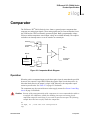
Comparator . . . . . . . . . . . . . . . . . . . . . . . . . . . . . . . . . . . . . . . . . . . . . . . . . . 135
Operation . . . . . . . . . . . . . . . . . . . . . . . . . . . . . . . . . . . . . . . . . . . . . . . . . . . . . 135
Comparator Control Register Definitions . . . . . . . . . . . . . . . . . . . . . . . . . . . . . 136
Temperature Sensor . . . . . . . . . . . . . . . . . . . . . . . . . . . . . . . . . . . . . . . . . . . 139
Temperature Sensor Operation . . . . . . . . . . . . . . . . . . . . . . . . . . . . . . . . . . . . 139
Flash Memory . . . . . . . . . . . . . . . . . . . . . . . . . . . . . . . . . . . . . . . . . . . . . . . . 141
Architecture . . . . . . . . . . . . . . . . . . . . . . . . . . . . . . . . . . . . . . . . . . . . . . . .
Flash Information Area . . . . . . . . . . . . . . . . . . . . . . . . . . . . . . . . . . . . . . . . . .
Operation . . . . . . . . . . . . . . . . . . . . . . . . . . . . . . . . . . . . . . . . . . . . . . . . . . . . .
Flash Operation Timing Using the Flash Frequency Registers . . . . . . . . .
Flash Code Protection Against External Access . . . . . . . . . . . . . . . . . . . .
Flash Code Protection Against Accidental Program and Erasure . . . . . . .
Byte Programming . . . . . . . . . . . . . . . . . . . . . . . . . . . . . . . . . . . . . . . . . . .
Page Erase . . . . . . . . . . . . . . . . . . . . . . . . . . . . . . . . . . . . . . . . . . . . . . . .
Mass Erase . . . . . . . . . . . . . . . . . . . . . . . . . . . . . . . . . . . . . . . . . . . . . . . .
Flash Controller Bypass . . . . . . . . . . . . . . . . . . . . . . . . . . . . . . . . . . . . . .
Flash Controller Behavior in DEBUG Mode . . . . . . . . . . . . . . . . . . . . . . .
Flash Control Register Definitions . . . . . . . . . . . . . . . . . . . . . . . . . . . . . . . . . .
Flash Control Register . . . . . . . . . . . . . . . . . . . . . . . . . . . . . . . . . . . . . . . .
Flash Status Register . . . . . . . . . . . . . . . . . . . . . . . . . . . . . . . . . . . . . . . .
Flash Page Select Register . . . . . . . . . . . . . . . . . . . . . . . . . . . . . . . . . . . .
PS022825-0908
141
142
143
145
145
145
147
147
147
148
148
149
149
150
150
Table of Contents
Z8 Encore! XP® F082A Series
Product Specification
ix
Flash Sector Protect Register . . . . . . . . . . . . . . . . . . . . . . . . . . . . . . . . . . 151
Flash Frequency High and Low Byte Registers . . . . . . . . . . . . . . . . . . . . 152
Flash Option Bits . . . . . . . . . . . . . . . . . . . . . . . . . . . . . . . . . . . . . . . . . . . . . . 153
Operation . . . . . . . . . . . . . . . . . . . . . . . . . . . . . . . . . . . . . . . . . . . . . . . . . . . . .
Option Bit Configuration By Reset . . . . . . . . . . . . . . . . . . . . . . . . . . . . . . .
Option Bit Types . . . . . . . . . . . . . . . . . . . . . . . . . . . . . . . . . . . . . . . . . . . .
Reading the Flash Information Page . . . . . . . . . . . . . . . . . . . . . . . . . . . . .
Flash Option Bit Control Register Definitions . . . . . . . . . . . . . . . . . . . . . . . . .
Trim Bit Address Register . . . . . . . . . . . . . . . . . . . . . . . . . . . . . . . . . . . . .
Trim Bit Data Register . . . . . . . . . . . . . . . . . . . . . . . . . . . . . . . . . . . . . . . .
Flash Option Bit Address Space . . . . . . . . . . . . . . . . . . . . . . . . . . . . . . . . . . .
Flash Program Memory Address 0000H . . . . . . . . . . . . . . . . . . . . . . . . . .
Flash Program Memory Address 0001H . . . . . . . . . . . . . . . . . . . . . . . . . .
Trim Bit Address Space . . . . . . . . . . . . . . . . . . . . . . . . . . . . . . . . . . . . . . . . . .
Trim Bit Address 0000H . . . . . . . . . . . . . . . . . . . . . . . . . . . . . . . . . . . . . .
Trim Bit Address 0001H . . . . . . . . . . . . . . . . . . . . . . . . . . . . . . . . . . . . . .
Trim Bit Address 0002H . . . . . . . . . . . . . . . . . . . . . . . . . . . . . . . . . . . . . .
Trim Bit Address 0003H . . . . . . . . . . . . . . . . . . . . . . . . . . . . . . . . . . . . . .
Trim Bit Address 0004H . . . . . . . . . . . . . . . . . . . . . . . . . . . . . . . . . . . . . .
Zilog Calibration Data . . . . . . . . . . . . . . . . . . . . . . . . . . . . . . . . . . . . . . . . . . .
ADC Calibration Data . . . . . . . . . . . . . . . . . . . . . . . . . . . . . . . . . . . . . . . .
Temperature Sensor Calibration Data . . . . . . . . . . . . . . . . . . . . . . . . . . . .
Watchdog Timer Calibration Data . . . . . . . . . . . . . . . . . . . . . . . . . . . . . . .
Serialization Data . . . . . . . . . . . . . . . . . . . . . . . . . . . . . . . . . . . . . . . . . . .
Randomized Lot Identifier . . . . . . . . . . . . . . . . . . . . . . . . . . . . . . . . . . . . .
153
153
154
155
155
155
156
156
156
158
158
158
159
159
159
161
161
161
164
164
165
166
Non-Volatile Data Storage . . . . . . . . . . . . . . . . . . . . . . . . . . . . . . . . . . . . . . 169
Operation . . . . . . . . . . . . . . . . . . . . . . . . . . . . . . . . . . . . . . . . . . . . . . . . . . . . .
NVDS Code Interface . . . . . . . . . . . . . . . . . . . . . . . . . . . . . . . . . . . . . . . . . . .
Byte Write . . . . . . . . . . . . . . . . . . . . . . . . . . . . . . . . . . . . . . . . . . . . . . . . .
Byte Read . . . . . . . . . . . . . . . . . . . . . . . . . . . . . . . . . . . . . . . . . . . . . . . . .
Power Failure Protection . . . . . . . . . . . . . . . . . . . . . . . . . . . . . . . . . . . . . .
Optimizing NVDS Memory Usage for Execution Speed . . . . . . . . . . . . . .
169
169
169
170
171
171
On-Chip Debugger . . . . . . . . . . . . . . . . . . . . . . . . . . . . . . . . . . . . . . . . . . . . 173
Architecture . . . . . . . . . . . . . . . . . . . . . . . . . . . . . . . . . . . . . . . . . . . . . . . . . . .
Operation . . . . . . . . . . . . . . . . . . . . . . . . . . . . . . . . . . . . . . . . . . . . . . . . . . . . .
OCD Interface . . . . . . . . . . . . . . . . . . . . . . . . . . . . . . . . . . . . . . . . . . . . . .
DEBUG Mode . . . . . . . . . . . . . . . . . . . . . . . . . . . . . . . . . . . . . . . . . . . . . .
PS022825-0908
173
174
174
175
Table of Contents
Z8 Encore! XP® F082A Series
Product Specification
x
OCD Data Format . . . . . . . . . . . . . . . . . . . . . . . . . . . . . . . . . . . . . . . . . . .
OCD Auto-Baud Detector/Generator . . . . . . . . . . . . . . . . . . . . . . . . . . . . .
OCD Serial Errors . . . . . . . . . . . . . . . . . . . . . . . . . . . . . . . . . . . . . . . . . . .
OCD Unlock Sequence (8-Pin Devices Only) . . . . . . . . . . . . . . . . . . . . . .
Breakpoints . . . . . . . . . . . . . . . . . . . . . . . . . . . . . . . . . . . . . . . . . . . . . . . .
Runtime Counter . . . . . . . . . . . . . . . . . . . . . . . . . . . . . . . . . . . . . . . . . . . .
On-Chip Debugger Commands . . . . . . . . . . . . . . . . . . . . . . . . . . . . . . . . . . . .
On-Chip Debugger Control Register Definitions . . . . . . . . . . . . . . . . . . . . . . .
OCD Control Register . . . . . . . . . . . . . . . . . . . . . . . . . . . . . . . . . . . . . . . .
OCD Status Register . . . . . . . . . . . . . . . . . . . . . . . . . . . . . . . . . . . . . . . . .
176
176
177
178
178
179
179
184
184
185
Oscillator Control . . . . . . . . . . . . . . . . . . . . . . . . . . . . . . . . . . . . . . . . . . . . . 187
Operation . . . . . . . . . . . . . . . . . . . . . . . . . . . . . . . . . . . . . . . . . . . . . . . . . . . . .
System Clock Selection . . . . . . . . . . . . . . . . . . . . . . . . . . . . . . . . . . . . . . .
Clock Failure Detection and Recovery . . . . . . . . . . . . . . . . . . . . . . . . . . .
Oscillator Control Register Definitions . . . . . . . . . . . . . . . . . . . . . . . . . . . . . . .
187
187
189
190
Crystal Oscillator . . . . . . . . . . . . . . . . . . . . . . . . . . . . . . . . . . . . . . . . . . . . . . 193
Operating Modes . . . . . . . . . . . . . . . . . . . . . . . . . . . . . . . . . . . . . . . . . . . . . . . 193
Crystal Oscillator Operation . . . . . . . . . . . . . . . . . . . . . . . . . . . . . . . . . . . . . . 193
Oscillator Operation with an External RC Network . . . . . . . . . . . . . . . . . . . . . 195
Internal Precision Oscillator . . . . . . . . . . . . . . . . . . . . . . . . . . . . . . . . . . . . . 197
Operation . . . . . . . . . . . . . . . . . . . . . . . . . . . . . . . . . . . . . . . . . . . . . . . . . . . . . 197
eZ8 CPU Instruction Set . . . . . . . . . . . . . . . . . . . . . . . . . . . . . . . . . . . . . . . . 199
Assembly Language Programming Introduction . . . . . . . . . . . . . . . . . . . . . . .
Assembly Language Syntax . . . . . . . . . . . . . . . . . . . . . . . . . . . . . . . . . . . . . .
eZ8 CPU Instruction Notation . . . . . . . . . . . . . . . . . . . . . . . . . . . . . . . . . . . . .
eZ8 CPU Instruction Classes . . . . . . . . . . . . . . . . . . . . . . . . . . . . . . . . . . . . .
eZ8 CPU Instruction Summary . . . . . . . . . . . . . . . . . . . . . . . . . . . . . . . . . . . .
199
200
200
202
207
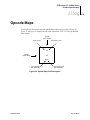
Opcode Maps . . . . . . . . . . . . . . . . . . . . . . . . . . . . . . . . . . . . . . . . . . . . . . . . . 216
Electrical Characteristics . . . . . . . . . . . . . . . . . . . . . . . . . . . . . . . . . . . . . . . 221
Absolute Maximum Ratings . . . . . . . . . . . . . . . . . . . . . . . . . . . . . . . . . . . . . . .
DC Characteristics . . . . . . . . . . . . . . . . . . . . . . . . . . . . . . . . . . . . . . . . . . . . .
AC Characteristics . . . . . . . . . . . . . . . . . . . . . . . . . . . . . . . . . . . . . . . . . . . . . .
On-Chip Peripheral AC and DC Electrical Characteristics . . . . . . . . . . . . . . .
General Purpose I/O Port Input Data Sample Timing . . . . . . . . . . . . . . . .
PS022825-0908
221
222
227
229
234
Table of Contents
Z8 Encore! XP® F082A Series
Product Specification
xi
General Purpose I/O Port Output Timing . . . . . . . . . . . . . . . . . . . . . . . . . 236
On-Chip Debugger Timing . . . . . . . . . . . . . . . . . . . . . . . . . . . . . . . . . . . . 237
UART Timing . . . . . . . . . . . . . . . . . . . . . . . . . . . . . . . . . . . . . . . . . . . . . . . 238
Packaging . . . . . . . . . . . . . . . . . . . . . . . . . . . . . . . . . . . . . . . . . . . . . . . . . . . 241
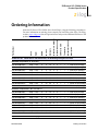
Ordering Information . . . . . . . . . . . . . . . . . . . . . . . . . . . . . . . . . . . . . . . . . . 251
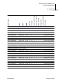
Index . . . . . . . . . . . . . . . . . . . . . . . . . . . . . . . . . . . . . . . . . . . . . . . . . . . . . . . . 261
Customer Support . . . . . . . . . . . . . . . . . . . . . . . . . . . . . . . . . . . . . . . . . . . . . 271
PS022825-0908
Table of Contents
Z8 Encore! XP® F082A Series
Product Specification
1
Overview
Zilog’s Z8 Encore!® MCU family of products are the first in a line of Zilog® microcontroller products based upon the 8-bit eZ8 CPU. Zilog’s Z8 Encore! XP® F082A Series
products expand upon Zilog’s extensive line of 8-bit microcontrollers. The Flash in-circuit
programming capability allows for faster development time and program changes in the
field. The new eZ8 CPU is upward compatible with existing Z8® instructions. The rich
peripheral set of the Z8 Encore! XP F082A Series makes it suitable for a variety of applications including motor control, security systems, home appliances, personal electronic
devices, and sensors.
Features
The key features of Z8 Encore! XP F082A Series products include:
PS022825-0908
•
•
•
•
•
•
•
•
•
•
•
•
20 MHz eZ8 CPU
•
Infrared Data Association (IrDA)-compliant infrared encoder/decoders, integrated
with UART
•
•
•
•
Two enhanced 16-bit timers with capture, compare, and PWM capability
1 KB, 2 KB, 4 KB, or 8 KB Flash memory with in-circuit programming capability
256 B, 512 B, or 1 KB register RAM
Up to 128 B non-volatile data storage (NVDS)
Internal precision oscillator trimmed to ±1% accuracy
External crystal oscillator, operating up to 20 MHz
Optional 8-channel, 10-bit analog-to-digital converter (ADC)
Optional on-chip temperature sensor
On-chip analog comparator
Optional on-chip low-power operational amplifier (LPO)
Full-duplex UART
The UART baud rate generator (BRG) can be configured and used as a basic 16-bit
timer
Watchdog Timer (WDT) with dedicated internal RC oscillator
Up to 20 vectored interrupts
6 to 25 I/O pins depending upon package
Overview
Z8 Encore! XP® F082A Series
Product Specification
2
•
•
•
•
•
•
Up to thirteen 5 V-tolerant input pins
•
•
•
•
Power-On Reset (POR)
Up to 8 ports capable of direct LED drive with no current limit resistor required
On-Chip Debugger (OCD)
Voltage Brownout (VBO) protection
Programmable low battery detection (LVD) (8-pin devices only)
Bandgap generated precision voltage references available for the ADC, comparator,
VBO, and LVD
2.7 V to 3.6 V operating voltage
8-, 20-, and 28-pin packages
0 °C to +70 °C and -40 °C to +105 °C for operating temperature ranges
Part Selection Guide
Table 1 on page 3 identifies the basic features and package styles available for each device
within the Z8 Encore! XP® F082A Series product line.
PS022825-0908
Overview
Z8 Encore! XP® F082A Series
Product Specification
3
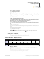
Table 1. Z8 Encore! XP® F082A Series Family Part Selection Guide
Part
Number
Flash RAM
(KB)
(B)
NVDS1
(B)
I/O
Comparator
Advanced ADC
Analog2 Inputs Packages
Z8F082A
8
1024
0
6–23
Yes
Yes
4–8
8-, 20- and 28-pin
Z8F081A
8
1024
0
6–25
Yes
No
0
8-, 20- and 28-pin
Z8F042A
4
1024
128
6–23
Yes
Yes
4–8
8-, 20- and 28-pin
Z8F041A
4
1024
128
6–25
Yes
No
0
8-, 20- and 28-pin
Z8F022A
2
512
64
6–23
Yes
Yes
4–8
8-, 20- and 28-pin
Z8F021A
2
512
64
6–25
Yes
No
0
8-, 20- and 28-pin
Z8F012A
1
256
16
6–23
Yes
Yes
4–8
8-, 20- and 28-pin
Z8F011A
1
256
16
6–25
Yes
No
0
8-, 20- and 28-pin
1Non-volatile
2Advanced
data storage.
Analog includes ADC, temperature sensor, and low-power operational amplifier.
PS022825-0908
Overview
Z8 Encore! XP® F082A Series
Product Specification
4
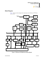
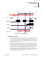
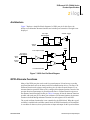
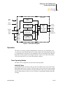
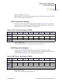
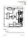
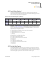
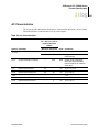
Block Diagram
Figure 1 displays the block diagram of the architecture of the Z8 Encore! XP® F082A
Series devices.
System
Clock
Oscillator
Control
XTAL/RC
Oscillator
Internal
Precision
Oscillator
Low Power
RC Oscillator
On-Chip
Debugger
eZ8
CPU
Interrupt
Controller
POR/VBO
and Reset
Controller
WDT
Memory Busses
Register Bus
UART
Timers
IrDA
Comparator
Temperature
Sensor
ADC
Low
Power
Op Amp
NVDS
Controller
Flash
Controller
Flash Memory
RAM
Controller
RAM
GPIO
Figure 1. Z8 Encore! XP F082A Series Block Diagram
PS022825-0908
Overview
Z8 Encore! XP® F082A Series
Product Specification
5
CPU and Peripheral Overview
eZ8 CPU Features
The eZ8 CPU, Zilog’s latest 8-bit Central Processing Unit (CPU), meets the continuing
demand for faster and more code-efficient microcontrollers. The eZ8 CPU executes a
superset of the original Z8® instruction set. The features of eZ8 CPU include:
•
Direct register-to-register architecture allows each register to function as an
accumulator, improving execution time and decreasing the required program
memory.
•
Software stack allows much greater depth in subroutine calls and interrupts than
hardware stacks.
•
•
•
Compatible with existing Z8 code.
•
•
Pipelined instruction fetch and execution.
•
•
•
•
New instructions support 12-bit linear addressing of the Register File.
Expanded internal Register File allows access of up to 4 KB.
New instructions improve execution efficiency for code developed using higherlevel programming languages, including C.
New instructions for improved performance including BIT, BSWAP, BTJ, CPC,
LDC, LDCI, LEA, MULT, and SRL.
Up to 10 MIPS operation.
C-Compiler friendly.
2 to 9 clock cycles per instruction.
For more information on eZ8 CPU, refer to eZ8 CPU Core User Manual (UM0128) available for download at www.zilog.com.
10-Bit Analog-to-Digital Converter
The optional analog-to-digital converter (ADC) converts an analog input signal to a 10-bit
binary number. The ADC accepts inputs from eight different analog input pins in both
single-ended and differential modes. The ADC also features a unity gain buffer when high
input impedance is required.
PS022825-0908
Overview
Z8 Encore! XP® F082A Series
Product Specification
6
Low-Power Operational Amplifier
The optional low-power operational amplifier (LPO) is a general-purpose amplifier
primarily targeted for current sense applications. The LPO output may be routed internally
to the ADC or externally to a pin.
Internal Precision Oscillator
The internal precision oscillator (IPO) is a trimmable clock source that requires no
external components.
Temperature Sensor
The optional temperature sensor produces an analog output proportional to the device temperature. This signal can be sent to either the ADC or the analog comparator.
Analog Comparator
The analog comparator compares the signal at an input pin with either an internal programmable voltage reference or a second input pin. The comparator output can be used to
drive either an output pin or to generate an interrupt.
External Crystal Oscillator
The crystal oscillator circuit provides highly accurate clock frequencies with the use of an
external crystal, ceramic resonator or RC network.
Low Voltage Detector
The low voltage detector (LVD) is able to generate an interrupt when the supply voltage
drops below a user-programmable level. The LVD is available on 8-pin devices only.
On-Chip Debugger
The Z8 Encore! XP® F082A Series products feature an integrated on-chip debugger
(OCD) accessed via a single-pin interface. The OCD provides a rich-set of debugging
capabilities, such as reading and writing registers, programming Flash memory, setting
breakpoints, and executing code.
PS022825-0908
Overview
Z8 Encore! XP® F082A Series
Product Specification
7
Universal Asynchronous Receiver/Transmitter
The full-duplex universal asynchronous receiver/transmitter (UART) is included in all Z8
Encore! XP package types. The UART supports 8- and 9-bit data modes and selectable
parity. The UART also supports multi-drop address processing in hardware. The UART
baud rate generator (BRG) can be configured and used as a basic 16-bit timer.
Timers
Two enhanced 16-bit reloadable timers can be used for timing/counting events or for
motor control operations. These timers provide a 16-bit programmable reload counter and
operate in ONE-SHOT, CONTINUOUS, GATED, CAPTURE, CAPTURE RESTART,
COMPARE, CAPTURE and COMPARE, PWM SINGLE OUTPUT and PWM DUAL
OUTPUT modes.
General-Purpose Input/Output
The Z8 Encore! XP F082A Series features 6 to 25 port pins (Ports A–D) for general- purpose input/output (GPIO). The number of GPIO pins available is a function of package,
and each pin is individually programmable. 5 V tolerant input pins are available on all
I/Os on 8-pin devices and most I/Os on other package types.
Direct LED Drive
The 20- and 28-pin devices support controlled current sinking output pins capable of
driving LEDs without the need for a current limiting resistor. These LED drivers are
independently programmable to four different intensity levels.
Flash Controller
The Flash Controller programs and erases Flash memory. The Flash Controller supports
several protection mechanisms against accidental program and erasure, as well as factory
serialization and read protection.
Non-Volatile Data Storage
The non-volatile data storage (NVDS) uses a hybrid hardware/software scheme to
implement a byte programmable data memory and is capable of over 100,000 write cycles.
Note:
PS022825-0908
Devices with 8 KB Flash memory do not include the NVDS feature.
Overview
Z8 Encore! XP® F082A Series
Product Specification
8
Interrupt Controller
The Z8 Encore! XP® F082A Series products support up to 20 interrupts. These
interrupts consist of 8 internal peripheral interrupts and 12 general-purpose I/O pin
interrupt sources. The interrupts have three levels of programmable interrupt priority.
Reset Controller
The Z8 Encore! XP F082A Series products can be reset using the RESET pin,
Power-On Reset, Watchdog Timer (WDT) time-out, STOP mode exit, or Voltage
Brownout (VBO) warning signal. The RESET pin is bi-directional, that is, it functions as
reset source as well as a reset indicator.
PS022825-0908
Overview
Z8 Encore! XP® F082A Series
Product Specification
9
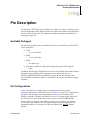
Pin Description
The Z8 Encore! XP® F082A Series products are available in a variety of packages styles
and pin configurations. This chapter describes the signals and available pin configurations
for each of the package styles. For information on physical package specifications, see
Packaging on page 241.
Available Packages
The following package styles are available for each device in the Z8 Encore! XP F082A
Series product line:
•
SOIC
– 8-, 20-, and 28-pin
•
PDIP
– 8-, 20-, and 28-pin
•
SSOP
– 20- and 28- pin
•
QFN (this is an MLF-S, a QFN style package with an 8-pin SOIC footprint)
– 8-pin
In addition, the Z8 Encore! XP F082A Series devices are available both with and without
advanced analog capability (ADC, temperature sensor and op amp). Devices
Z8F082A, Z8F042A, Z8F022A, and Z8F012A contain the advanced analog, while
devices Z8F081A, Z8F041A, Z8F021A, and Z8F011A do not have the advanced analog
capability.
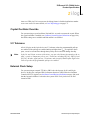
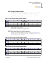
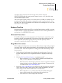
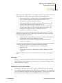
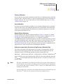
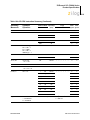
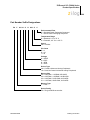
Pin Configurations
Figure 2 through Figure 4 display the pin configurations for all the packages
available in the Z8 Encore! XP F082A Series. See Table 2 on page 11 for a description of
the signals. The analog input alternate functions (ANAx) are not available on the
Z8F081A, Z8F041A, Z8F021A, and Z8F011A devices. The analog supply pins (AVDD
and AVSS) are also not available on these parts, and are replaced by PB6 and PB7.
At reset, all Port A, B and C pins default to an input state. In addition, any alternate
functionality is not enabled, so the pins function as general purpose input ports until
programmed otherwise. At powerup, the PD0 pin defaults to the RESET alternate
function.
PS022825-0908
Pin Description
Z8 Encore! XP® F082A Series
Product Specification
10
The pin configurations listed are preliminary and subject to change based on
manufacturing limitations.
VDD
PA0/T0IN/T0OUT/XIN//DBG
PA1/T0OUT/XOUT/ANA3/VREF/CLKIN
PA2/RESET/DE0/T1OUT
1
2
3
4
8
7
6
5
VSS
PA5/TXD0/T1OUT/ANA0/CINP/AMPOUT
PA4/RXD0/ANA1/CINN/AMPINN
PA3/CTS0/ANA2/COUT/AMPINP/T1IN
Figure 2. Z8F08xA, Z8F04xA, Z8F02xA, and Z8F01xA in 8-Pin SOIC, QFN/MLF-S, or PDIP Package
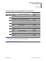
PB1/ANA1/AMPINN
PB2/ANA2/AMPINP
PB3/CLKIN/ANA3
VDD
PA0/T0IN/T0OUT/XIN
PA1/T0OUT/XOUT
VSS
PA2/DE0
PA3/CTS0
PA4/RXD0
1
2
3
4
5
6
7
8
9
10
20
19
18
17
16
15
14
13
12
11
PB0/ANA0/AMPOUT
PC3/COUT/LED
PC2/ANA6/LED/VREF
PC1/ANA5/CINN/LED
PC0/ANA4/CINP/LED
DBG
RESET/PD0
PA7/T1OUT
PA6/T1IN/T1OUT
PA5/TXD0
Figure 3. Z8F08xA, Z8F04xA, Z8F02xA, and Z8F01xA in 20-Pin SOIC, SSOP or PDIP Package
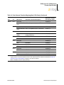
PB2/ANA2/AMPINP
PB4/ANA7
PB5/VREF
PB3/CLKIN/ANA3
(PB6) AVDD
VDD
PA0/T0IN/T0OUT/XIN
PA1/T0OUT/XOUT
VSS
(PB7) AVSS
PA2/DE0
PA3/CTS0
PA4/RXD0
PA5/TXD0
1
2
3
4
5
6
7
8
9
10
11
12
13
14
28
27
26
25
24
23
22
21
20
19
18
17
16
15
PB1/ANA1/AMPINN
PB0/ANA0/AMPOUT
PC3/COUT/LED
PC2/ANA6/LED
PC1/ANA5/CINN/LED
PC0/ANA4/CINP/LED
DBG
RESET/PD0
PC7/LED
PC6/LED
PA7/T1OUT
PC5/LED
PC4/LED
PA6/T1IN/T1OUT
Figure 4. Z8F08xA, Z8F04xA, Z8F02xA, and Z8F01xA in 28-Pin SOIC, SSOP or PDIP Package
PS022825-0908
Pin Description
Z8 Encore! XP® F082A Series
Product Specification
11
Signal Descriptions
Table 2 describes the Z8 Encore! XP F082A Series signals. See Pin Configurations on
page 9 to determine the signals available for the specific package styles.
Table 2. Signal Descriptions
Signal Mnemonic
I/O
Description
General-Purpose I/O Ports A–D
PA[7:0]
I/O
Port A. These pins are used for general-purpose I/O.
PB[7:0]
I/O
Port B. These pins are used for general-purpose I/O. PB6 and PB7 are
available only in those devices without an ADC.
PC[7:0]
I/O
Port C. These pins are used for general-purpose I/O.
PD[0]
I/O
Port D. This pin is used for general-purpose output only.
Note: PB6 and PB7 are only available in 28-pin packages without ADC. In 28-pin packages with ADC, they are
replaced by AVDD and AVSS.
UART Controllers
TXD0
O
Transmit Data. This signal is the transmit output from the UART and IrDA.
RXD0
I
Receive Data. This signal is the receive input for the UART and IrDA.
CTS0
I
Clear To Send. This signal is the flow control input for the UART.
DE
O
Driver Enable. This signal allows automatic control of external RS-485
drivers. This signal is approximately the inverse of the TXE (Transmit
Empty) bit in the UART Status 0 register. The DE signal may be used to
ensure the external RS-485 driver is enabled when data is transmitted by
the UART.
T0OUT/T1OUT
O
Timer Output 0–1. These signals are outputs from the timers.
T0OUT/T1OUT
O
Timer Complement Output 0–1. These signals are output from the timers
in PWM Dual Output mode.
T0IN/T1IN
I
Timer Input 0–1. These signals are used as the capture, gating and
counter inputs.
CINP/CINN
I
Comparator Inputs. These signals are the positive and negative inputs to
the comparator.
COUT
O
Comparator Output.
Timers
Comparator
PS022825-0908
Pin Description
Z8 Encore! XP® F082A Series
Product Specification
12
Table 2. Signal Descriptions (Continued)
Signal Mnemonic
I/O
Description
Analog
ANA[7:0]
VREF
I
I/O
Analog Port. These signals are used as inputs to the analog-to-digital
converter (ADC).
Analog-to-digital converter reference voltage input, or buffered output for
internal reference.
Low-Power Operational Amplifier (LPO)
AMPINP/AMPINN
I
LPO inputs. If enabled, these pins drive the positive and negative amplifier
inputs respectively.
AMPOUT
O
LPO output. If enabled, this pin is driven by the on-chip LPO.
XIN
I
External Crystal Input. This is the input pin to the crystal oscillator. A
crystal can be connected between it and the XOUT pin to form the
oscillator. In addition, this pin is used with external RC networks or external
clock drivers to provide the system clock.
XOUT
O
External Crystal Output. This pin is the output of the crystal oscillator. A
crystal can be connected between it and the XIN pin to form the oscillator.
I
Clock Input Signal. This pin may be used to input a TTL-level signal to be
used as the system clock.
O
Direct LED drive capability. All port C pins have the capability to drive an
LED without any other external components. These pins have
programmable drive strengths set by the GPIO block.
I/O
Debug. This signal is the control and data input and output to and from the
On-Chip Debugger.
Oscillators
Clock Input
CLKIN
LED Drivers
LED
On-Chip Debugger
DBG
Caution: The DBG pin is open-drain and requires a pull-up resistor to ensure proper operation.
Reset
RESET
PS022825-0908
I/O
RESET. Generates a Reset when asserted (driven Low). Also serves as a
reset indicator; the Z8 Encore! XP forces this pin low when in reset. This
pin is open-drain and features an enabled internal pull-up resistor.
Pin Description
Z8 Encore! XP® F082A Series
Product Specification
13
Table 2. Signal Descriptions (Continued)
Signal Mnemonic
I/O
Description
Power Supply
VDD
I
Digital Power Supply.
AVDD
I
Analog Power Supply.
VSS
I
Digital Ground.
AVSS
I
Analog Ground.
Note: The AVDD and AVSS signals are available only in 28-pin packages with ADC. They are replaced by PB6 and
PB7 on 28-pin packages without ADC.
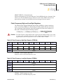
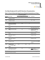
Pin Characteristics
Table 3 describes the characteristics for each pin available on the Z8 Encore! XP F082A
Series 20- and 28-pin devices. Data in Table 3 is sorted alphabetically by the pin symbol
mnemonic.
Table 4 on page 14 provides detailed information about the characteristics for each pin
available on the Z8 Encore! XP F082A Series 8-pin devices.
All six I/O pins on the 8-pin packages are 5 V-tolerant (unless the pull-up devices are
enabled). The column in Table 3 below describes 5 V-tolerance for the 20- and 28-pin
packages only.
Note:
Table 3. Pin Characteristics (20- and 28-pin Devices)
Direction
Reset
Direction
Active
Low
or
Active
High
Tristate
Output
AVDD
N/A
N/A
N/A
N/A
N/A
AVSS
N/A
N/A
N/A
N/A
DBG
I/O
I
N/A
PA[7:0]
I/O
I
PB[7:0]
I/O
I
Symbol
Mnemonic
PS022825-0908
Internal Pull- Schmittup
Trigger
or Pull-down
Input
Open Drain
Output
5V
Tolerance
N/A
N/A
N/A
N/A
N/A
N/A
NA
Yes
Yes
Yes
Yes
No
N/A
Yes
Programmable
Pull-up
Yes
Yes,
Programmable
PA[7:2]
unless
pullups
enabled
N/A
Yes
Programmable
Pull-up
Yes
Yes,
Programmable
PB[7:6]
unless
pullups
enabled
Pin Description
Z8 Encore! XP® F082A Series
Product Specification
14
Table 3. Pin Characteristics (20- and 28-pin Devices) (Continued)
Direction
Reset
Direction
Active
Low
or
Active
High
Tristate
Output
PC[7:0]
I/O
I
N/A
Yes
RESET/PD0
I/O
I/O (defaults
to RESET)
Low (in
Reset
mode)
VDD
N/A
N/A
N/A
N/A
N/A
N/A
VSS
N/A
N/A
N/A
N/A
N/A
N/A
Open Drain
Output
5V
Tolerance
Symbol
Mnemonic
Internal Pull- Schmittup
Trigger
or Pull-down
Input
Open Drain
Output
5V
Tolerance
PC[7:3]
unless
pullups
enabled
Programmable
Pull-up
Yes
Yes,
Programmable
Yes (PD0 Programmable
only)
for PD0; always
on for RESET
Yes
Programmable Yes, unless
for PD0; always
pullups
on for RESET
enabled
PB6 and PB7 are available only in those devices without ADC.
Note:
Table 4. Pin Characteristics (8-Pin Devices)
)
Symbol
Mnemonic
Direction
Reset
Direction
Active
Low
or
Active
High
Tristate
Output
Internal Pullup
or Pull-down
SchmittTrigger
Input
PA0/DBG
I/O
I (but can
change
during reset
if key
sequence
detected)
N/A
Yes
Programmable
Pull-up
Yes
Yes,
Yes, unless
Programmable
pull-ups
enabled
PA1
I/O
I
N/A
Yes
Programmable
Pull-up
Yes
Yes,
Yes, unless
Programmable
pull-ups
enabled
RESET/PA2
I/O
I/O (defaults
to RESET)
Low (in
Reset
mode)
Yes
Programmable
for PA2; always
on for RESET
Yes
Programmable Yes, unless
for PA2; always
pull-ups
on for RESET
enabled
PA[5:3]
I/O
I
N/A
Yes
Programmable
Pull-up
Yes
Yes,
Yes, unless
Programmable
pull-ups
enabled
VDD
N/A
N/A
N/A
N/A
N/A
N/A
N/A
N/A
VSS
N/A
N/A
N/A
N/A
N/A
N/A
N/A
N/A
PS022825-0908
Pin Description
Z8 Encore! XP® F082A Series
Product Specification
15
Address Space
The eZ8 CPU can access the following three distinct address spaces:
1. The Register File contains addresses for the general-purpose registers and the eZ8
CPU, peripheral, and general-purpose I/O port control registers.
2. The Program Memory contains addresses for all memory locations having executable
code and/or data.
3. The Data Memory contains addresses for all memory locations that contain data only.
These three address spaces are covered briefly in the following subsections. For more
information on eZ8 CPU and its address space, refer to eZ8 CPU Core User Manual
(UM0128) available for download at www.zilog.com.
Register File
The Register File address space in the Z8 Encore!® MCU is 4 KB (4096 bytes). The
Register File is composed of two sections: control registers and general-purpose registers.
When instructions are executed, registers defined as sources are read, and registers defined
as destinations are written. The architecture of the eZ8 CPU allows all general-purpose
registers to function as accumulators, address pointers, index registers, stack areas, or
scratch pad memory.
The upper 256 bytes of the 4 KB Register File address space are reserved for control of the
eZ8 CPU, the on-chip peripherals, and the I/O ports. These registers are located at
addresses from F00H to FFFH. Some of the addresses within the 256 B control register
section are reserved (unavailable). Reading from a reserved Register File address returns
an undefined value. Writing to reserved Register File addresses is not recommended and
can produce unpredictable results.
The on-chip RAM always begins at address 000H in the Register File address space. The
Z8 Encore! XP® F082A Series devices contain 256 B to 1 KB of on-chip RAM.
Reading from Register File addresses outside the available RAM addresses (and not
within the control register address space) returns an undefined value. Writing to these
Register File addresses produces no effect.
Program Memory
The eZ8 CPU supports 64 KB of Program Memory address space. The Z8 Encore! XP
F082A Series devices contain 1 KB to 8 KB of on-chip Flash memory in the Program
Memory address space, depending on the device. Reading from Program Memory
PS022825-0908
Address Space
Z8 Encore! XP® F082A Series
Product Specification
16
addresses outside the available Flash memory addresses returns FFH. Writing to these
unimplemented Program Memory addresses produces no effect. Table 5 describes the
Program Memory Maps for the Z8 Encore! XP F082A Series products.
Table 5. Z8 Encore! XP F082A Series Program Memory Maps
Program Memory Address (Hex)
Function
Z8F082A and Z8F081A Products
0000–0001
Flash Option Bits
0002–0003
Reset Vector
0004–0005
WDT Interrupt Vector
0006–0007
Illegal Instruction Trap
0008–0037
Interrupt Vectors*
0038–0039
Reserved
003A–003D
Oscillator Fail Trap Vectors
003E–1FFF
Program Memory
Z8F042A and Z8F041A Products
PS022825-0908
0000–0001
Flash Option Bits
0002–0003
Reset Vector
0004–0005
WDT Interrupt Vector
0006–0007
Illegal Instruction Trap
0008–0037
Interrupt Vectors*
0038–0039
Reserved
003A–003D
Oscillator Fail Trap Vectors
003E–0FFF
Program Memory
Address Space
Z8 Encore! XP® F082A Series
Product Specification
17
Table 5. Z8 Encore! XP F082A Series Program Memory Maps (Continued)
Program Memory Address (Hex)
Function
Z8F022A and Z8F021A Products
0000–0001
Flash Option Bits
0002–0003
Reset Vector
0004–0005
WDT Interrupt Vector
0006–0007
Illegal Instruction Trap
0008–0037
Interrupt Vectors*
0038–0039
Reserved
003A–003D
Oscillator Fail Trap Vectors
003E–07FF
Program Memory
Z8F012A and Z8F011A Products
0000–0001
Flash Option Bits
0002–0003
Reset Vector
0004–0005
WDT Interrupt Vector
0006–0007
Illegal Instruction Trap
0008–0037
Interrupt Vectors*
0038–0039
Reserved
003A–003D
Oscillator Fail Trap Vectors
003E–03FF
Program Memory
* See Table
32 on page 56 for a list of the interrupt vectors.
Data Memory
The Z8 Encore! XP F082A Series does not use the eZ8 CPU’s 64 KB Data Memory
address space.
Flash Information Area
Table 6 on page 18 describes the Z8 Encore! XP F082A Series Flash Information Area.
This 128 B Information Area is accessed by setting bit 7 of the Flash Page Select Register
to 1. When access is enabled, the Flash Information Area is mapped into the Program
Memory and overlays the 128 bytes at addresses FE00H to FF7FH. When the Information
Area access is enabled, all reads from these Program Memory addresses return the InforPS022825-0908
Address Space
Z8 Encore! XP® F082A Series
Product Specification
18
mation Area data rather than the Program Memory data. Access to the Flash Information
Area is read-only.
Table 6. Z8 Encore! XP F082A Series Flash Memory Information Area Map
Program Memory Address (Hex) Function
PS022825-0908
FE00–FE3F
Zilog Option Bits/Calibration Data
FE40–FE53
Part Number
20-character ASCII alphanumeric code
Left justified and filled with FFH
FE54–FE5F
Reserved
FE60–FE7F
Zilog Calibration Data
FE80–FFFF
Reserved
Address Space
Z8 Encore! XP® F082A Series
Product Specification
19
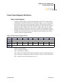
Register Map
Table 7 provides the address map for the Register File of the Z8 Encore! XP® F082A
Series devices. Not all devices and package styles in the Z8 Encore! XP F082A Series
support the ADC, or all of the GPIO Ports. Consider registers for unimplemented peripherals as Reserved.
Table 7. Register File Address Map
Address (Hex) Register Description
Mnemonic
Reset (Hex)
Page No
General-Purpose RAM
Z8F082A/Z8F081A Devices
000–3FF
General-Purpose Register File RAM
—
XX
400–EFF
Reserved
—
XX
Z8F042A/Z8F041A Devices
000–3FF
General-Purpose Register File RAM
—
XX
400–EFF
Reserved
—
XX
Z8F022A/Z8F021A Devices
000–1FF
General-Purpose Register File RAM
—
XX
200–EFF
Reserved
—
XX
Z8F012A/Z8F011A Devices
000–0FF
General-Purpose Register File RAM
—
XX
100–EFF
Reserved
—
XX
F00
Timer 0 High Byte
T0H
00
87
F01
Timer 0 Low Byte
T0L
01
87
F02
Timer 0 Reload High Byte
T0RH
FF
88
F03
Timer 0 Reload Low Byte
T0RL
FF
88
F04
Timer 0 PWM High Byte
T0PWMH
00
88
Timer 0
F05
Timer 0 PWM Low Byte
T0PWML
00
89
F06
Timer 0 Control 0
T0CTL0
00
83
F07
Timer 0 Control 1
T0CTL1
00
84
F08
Timer 1 High Byte
T1H
00
87
F09
Timer 1 Low Byte
T1L
01
87
F0A
Timer 1 Reload High Byte
T1RH
FF
88
Timer 1
XX=Undefined
PS022825-0908
Register Map
Z8 Encore! XP® F082A Series
Product Specification
20
Table 7. Register File Address Map (Continued)
Address (Hex) Register Description
Mnemonic
Reset (Hex)
Page No
F0B
Timer 1 Reload Low Byte
T1RL
FF
88
F0C
Timer 1 PWM High Byte
T1PWMH
00
88
F0D
Timer 1 PWM Low Byte
T1PWML
00
89
F0E
Timer 1 Control 0
T1CTL0
00
83
F0F
Timer 1 Control 1
T1CTL1
00
84
F10–F6F
Reserved
—
XX
F40
UART Transmit/Receive Data Registers
TXD, RXD
XX
113
F41
UART Status 0 Register
U0STAT0
00
111
F42
UART Control 0 Register
U0CTL0
00
108
F43
UART Control 1 Register
U0CTL1
00
108
F44
UART Status 1 Register
U0STAT1
00
112
F45
UART Address Compare Register
U0ADDR
00
114
F46
UART Baud Rate High Byte Register
U0BRH
FF
114
F47
UART Baud Rate Low Byte Register
U0BRL
FF
114
ADC Control 0
ADCCTL0
00
130
F71
ADC Control 1
ADCCTL1
80
130
F72
ADC Data High Byte
ADCD_H
XX
133
F73
ADC Data Low Bits
ADCD_L
XX
133
F74–F7F
Reserved
—
XX
UART
Analog-to-Digital Converter (ADC)
F70
Low Power Control
F80
Power Control 0
PWRCTL0
80
35
F81
Reserved
—
XX
F82
LED Drive Enable
LEDEN
00
52
F83
LED Drive Level High Byte
LEDLVLH
00
53
F84
LED Drive Level Low Byte
LEDLVLL
00
54
F85
Reserved
—
XX
LED Controller
Oscillator Control
F86
Oscillator Control
OSCCTL
A0
F87–F8F
Reserved
—
XX
Comparator 0 Control
CMP0
14
190
Comparator 0
F90
136
XX=Undefined
PS022825-0908
Register Map
Z8 Encore! XP® F082A Series
Product Specification
21
Table 7. Register File Address Map (Continued)
Address (Hex) Register Description
Mnemonic
Reset (Hex)
F91–FBF
—
XX
Reserved
Page No
Interrupt Controller
FC0
Interrupt Request 0
IRQ0
00
60
FC1
IRQ0 Enable High Bit
IRQ0ENH
00
63
FC2
IRQ0 Enable Low Bit
IRQ0ENL
00
63
FC3
Interrupt Request 1
IRQ1
00
61
FC4
IRQ1 Enable High Bit
IRQ1ENH
00
64
FC5
IRQ1 Enable Low Bit
IRQ1ENL
00
64
FC6
Interrupt Request 2
IRQ2
00
62
FC7
IRQ2 Enable High Bit
IRQ2ENH
00
65
FC8
IRQ2 Enable Low Bit
IRQ2ENL
00
65
FC9–FCC
Reserved
—
XX
FCD
Interrupt Edge Select
IRQES
00
67
FCE
Shared Interrupt Select
IRQSS
00
67
FCF
Interrupt Control
IRQCTL
00
67
Port A Address
PAADDR
00
45
GPIO Port A
FD0
FD1
Port A Control
PACTL
00
47
FD2
Port A Input Data
PAIN
XX
47
FD3
Port A Output Data
PAOUT
00
47
FD4
Port B Address
PBADDR
00
45
FD5
Port B Control
PBCTL
00
47
FD6
Port B Input Data
PBIN
XX
47
FD7
Port B Output Data
PBOUT
00
47
FD8
Port C Address
PCADDR
00
45
FD9
Port C Control
PCCTL
00
47
FDA
Port C Input Data
PCIN
XX
47
FDB
Port C Output Data
PCOUT
00
47
FDC
Port D Address
PDADDR
00
45
FDD
Port D Control
PDCTL
00
47
FDE
Reserved
—
XX
GPIO Port B
GPIO Port C
GPIO Port D
XX=Undefined
PS022825-0908
Register Map
Z8 Encore! XP® F082A Series
Product Specification
22
Table 7. Register File Address Map (Continued)
Address (Hex) Register Description
Mnemonic
Reset (Hex)
Page No
FDF
Port D Output Data
PDOUT
00
47
FE0–FEF
Reserved
—
XX
Watchdog Timer (WDT)
FF0
Reset Status (Read-only)
RSTSTAT
X0
30
Watchdog Timer Control (Write-only)
WDTCTL
N/A
94
FF1
Watchdog Timer Reload Upper Byte
WDTU
00
95
FF2
Watchdog Timer Reload High Byte
WDTH
04
95
95
FF3
Watchdog Timer Reload Low Byte
WDTL
00
FF4–FF5
Reserved
—
XX
Trim Bit Control
FF6
Trim Bit Address
TRMADR
00
155
FF7
Trim Bit Data
TRMDR
00
156
Flash Memory Controller
FF8
Flash Control
FCTL
00
149
FF8
Flash Status
FSTAT
00
150
Flash Page Select
FPS
00
151
Flash Sector Protect
FPROT
00
151
FF9
FFA
Flash Programming Frequency High Byte FFREQH
00
152
FFB
Flash Programming Frequency Low Byte FFREQL
00
152
Flags
XX
Refer to eZ8
CPU Core
User Manual
(UM0128)
eZ8 CPU
FFC
—
FFD
Register Pointer
RP
XX
FFE
Stack Pointer High Byte
SPH
XX
FFF
Stack Pointer Low Byte
SPL
XX
XX=Undefined
PS022825-0908
Register Map
Z8 Encore! XP® F082A Series
Product Specification
23
Reset, Stop Mode Recovery, and Low
Voltage Detection
The Reset Controller within the Z8 Encore! XP® F082A Series controls Reset and Stop
Mode Recovery operation and provides indication of low supply voltage conditions. In
typical operation, the following events cause a Reset:
•
•
•
Power-On Reset (POR)
•
External RESET pin assertion (when the alternate RESET function is enabled by
the GPIO register)
•
On-chip debugger initiated Reset (OCDCTL[0] set to 1)
Voltage Brownout (VBO)
Watchdog Timer time-out (when configured by the WDT_RES Flash Option Bit
to initiate a reset)
When the device is in STOP mode, a Stop Mode Recovery is initiated by either of the
following:
•
•
Watchdog Timer time-out
GPIO Port input pin transition on an enabled Stop Mode Recovery source
The low voltage detection circuitry on the device (available on the 8-pin product versions
only) performs the following functions:
•
Generates the VBO reset when the supply voltage drops below a minimum safe
level.
•
Generates an interrupt when the supply voltage drops below a user-defined level
(8-pin devices only).
Reset Types
The Z8 Encore! XP F082A Series provides several different types of Reset operation. Stop
Mode Recovery is considered as a form of Reset. Table 8 lists the types of Reset and their
operating characteristics. The System Reset is longer if the external crystal oscillator is
enabled by the Flash option bits, allowing additional time for oscillator start-up.
PS022825-0908
Reset, Stop Mode Recovery, and Low Voltage Detection
Z8 Encore! XP® F082A Series
Product Specification
24
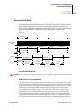
Table 8. Reset and Stop Mode Recovery Characteristics and Latency
Reset Characteristics and Latency
Reset Type
Control Registers
eZ8
CPU Reset Latency (Delay)
System Reset
Reset (as applicable)
Reset 66 Internal Precision Oscillator Cycles
System Reset with Crystal Reset (as applicable)
Oscillator Enabled
Reset 5000 Internal Precision Oscillator Cycles
Stop Mode Recovery
Reset 66 Internal Precision Oscillator Cycles
+ IPO startup time
Unaffected, except
WDT_CTL and
OSC_CTL registers
Stop Mode Recovery with Unaffected, except
Crystal Oscillator Enabled WDT_CTL and
OSC_CTL registers
Reset 5000 Internal Precision Oscillator Cycles
During a System Reset or Stop Mode Recovery, the Internal Precision Oscillator requires
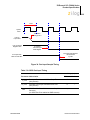
4 µs to start up. Then the Z8 Encore! XP F082A Series device is held in Reset for 66
cycles of the Internal Precision Oscillator. If the crystal oscillator is enabled in the Flash
option bits, this reset period is increased to 5000 IPO cycles. When a reset occurs because
of a low voltage condition or Power-On Reset (POR), this delay is measured from the time
that the supply voltage first exceeds the POR level. If the external pin reset remains
asserted at the end of the reset period, the device remains in reset until the pin is deasserted.
At the beginning of Reset, all GPIO pins are configured as inputs with pull-up resistor disabled, except PD0 (or PA2 on 8-pin devices) which is shared with the reset pin. On reset,
the PD0 is configured as a bidirectional open-drain reset. The pin is internally driven low
during port reset, after which the user code may reconfigure this pin as a general purpose
output.
During Reset, the eZ8 CPU and on-chip peripherals are idle; however, the on-chip crystal
oscillator and Watchdog Timer oscillator continue to run.
Upon Reset, control registers within the Register File that have a defined Reset value are
loaded with their reset values. Other control registers (including the Stack Pointer,
Register Pointer, and Flags) and general-purpose RAM are undefined following Reset.
The eZ8 CPU fetches the Reset vector at Program Memory addresses 0002H and 0003H
and loads that value into the Program Counter. Program execution begins at the Reset
vector address.
As the control registers are re-initialized by a system reset, the system clock after reset is
always the IPO. The software must reconfigure the oscillator control block, such that the
correct system clock source is enabled and selected.
PS022825-0908
Reset, Stop Mode Recovery, and Low Voltage Detection
Z8 Encore! XP® F082A Series
Product Specification
25
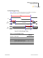
Reset Sources
Table 9 lists the possible sources of a system reset.
Table 9. Reset Sources and Resulting Reset Type
Operating Mode
Reset Source
Special Conditions
NORMAL or HALT
modes
Power-On Reset/Voltage
Brownout
Reset delay begins after supply voltage
exceeds POR level.
Watchdog Timer time-out
when configured for Reset
None.
RESET pin assertion
All reset pulses less than three system clocks
in width are ignored.
On-Chip Debugger initiated Reset System Reset, except the On-Chip Debugger
(OCDCTL[0] set to 1)
is unaffected by the reset.
STOP mode
Power-On Reset/Voltage
Brownout
Reset delay begins after supply voltage
exceeds POR level.
RESET pin assertion
All reset pulses less than the specified analog
delay are ignored. See Table 131 on
page 229.
DBG pin driven Low
None.
Power-On Reset
Z8 Encore! XP F082A Series devices contain an internal Power-On Reset
circuit. The POR circuit monitors the supply voltage and holds the device in the Reset
state until the supply voltage reaches a safe operating level. After the supply voltage
exceeds the POR voltage threshold (VPOR), the device is held in the Reset state until the
POR Counter has timed out. If the crystal oscillator is enabled by the option bits, this
timeout is longer.
After the Z8 Encore! XP F082A Series device exits the Power-On Reset state, the eZ8
CPU fetches the Reset vector. Following Power-On Reset, the POR status bit in the Reset
Status (RSTSTAT) register is set to 1.
Figure 5 displays Power-On Reset operation. See Electrical Characteristics on page 221
for the POR threshold voltage (VPOR).
PS022825-0908
Reset, Stop Mode Recovery, and Low Voltage Detection
Z8 Encore! XP® F082A Series
Product Specification
26
VCC = 3.3 V
VPOR
VVBO
Program
Execution
VCC = 0.0 V
Internal Precision
Oscillator
Crystal
Oscillator
Oscillator
Start-up
Internal RESET
signal
POR
counter delay
Note: Not to Scale
optional XTAL
counter delay
Figure 5. Power-On Reset Operation
Voltage Brownout Reset
The devices in the Z8 Encore! XP F082A Series provide low Voltage Brownout (VBO)
protection. The VBO circuit senses when the supply voltage drops to an unsafe level
(below the VBO threshold voltage) and forces the device into the Reset state. While the
supply voltage remains below the Power-On Reset voltage threshold (VPOR), the VBO
block holds the device in the Reset.
After the supply voltage again exceeds the Power-On Reset voltage threshold, the device
progresses through a full System Reset sequence, as described in the Power-On Reset
section. Following Power-On Reset, the POR status bit in the Reset Status (RSTSTAT)
register is set to 1. Figure 6 displays Voltage Brownout operation. See Electrical Characteristics on page 221 for the VBO and POR threshold voltages (VVBO and VPOR).
The Voltage Brownout circuit can be either enabled or disabled during STOP mode.
Operation during STOP mode is set by the VBO_AO Flash Option Bit. See Flash Option
Bits for information about configuring VBO_AO.
PS022825-0908
Reset, Stop Mode Recovery, and Low Voltage Detection
Z8 Encore! XP® F082A Series
Product Specification
27
VCC = 3.3 V
VCC = 3.3 V
VPOR
VVBO
Program
Execution
Voltage
Brownout
Program
Execution
System Clock
Internal RESET
signal
POR
counter delay
Note: Not to Scale
Figure 6. Voltage Brownout Reset Operation
The POR level is greater than the VBO level by the specified hysteresis value. This
ensures that the device undergoes a Power-On Reset after recovering from a VBO
condition.
Watchdog Timer Reset
If the device is in NORMAL or HALT mode, the Watchdog Timer can initiate a System
Reset at time-out if the WDT_RES Flash Option Bit is programmed to 1. This is the
unprogrammed state of the WDT_RES Flash Option Bit. If the bit is programmed to 0, it
configures the Watchdog Timer to cause an interrupt, not a System Reset, at time-out.
The WDT bit in the Reset Status (RSTSTAT) register is set to signify that the reset was
initiated by the Watchdog Timer.
External Reset Input
The RESET pin has a Schmitt-Triggered input and an internal pull-up resistor. Once the
RESET pin is asserted for a minimum of four system clock cycles, the device progresses
through the System Reset sequence. Because of the possible asynchronicity of the system
clock and reset signals, the required reset duration may be as short as three clock periods
PS022825-0908
Reset, Stop Mode Recovery, and Low Voltage Detection
Z8 Encore! XP® F082A Series
Product Specification
28
and as long as four. A reset pulse three clock cycles in duration might trigger a reset; a
pulse four cycles in duration always triggers a reset.
While the RESET input pin is asserted Low, the Z8 Encore! XP® F082A Series devices
remain in the Reset state. If the RESET pin is held Low beyond the System Reset timeout, the device exits the Reset state on the system clock rising edge following RESET pin
deassertion. Following a System Reset initiated by the external RESET pin, the EXT status bit in the Reset Status (RSTSTAT) register is set to 1.
External Reset Indicator
During System Reset or when enabled by the GPIO logic (see Port A–D Control Registers
on page 46), the RESET pin functions as an open-drain (active Low) reset mode indicator
in addition to the input functionality. This reset output feature allows a
Z8 Encore! XP F082A Series device to reset other components to which it is connected,
even if that reset is caused by internal sources such as POR, VBO or WDT events.
After an internal reset event occurs, the internal circuitry begins driving the RESET pin
Low. The RESET pin is held Low by the internal circuitry until the appropriate delay
listed in Table 8 has elapsed.
On-Chip Debugger Initiated Reset
A Power-On Reset can be initiated using the On-Chip Debugger by setting the RST bit in
the OCD Control register. The On-Chip Debugger block is not reset but the rest of the chip
goes through a normal system reset. The RST bit automatically clears during the system
reset. Following the system reset the POR bit in the Reset Status (RSTSTAT) register is set.
Stop Mode Recovery
STOP mode is entered by execution of a STOP instruction by the eZ8 CPU. See LowPower Modes on page 33 for detailed STOP mode information. During Stop Mode Recovery (SMR), the CPU is held in reset for 66 IPO cycles if the crystal oscillator is disabled or
5000 cycles if it is enabled. The SMR delay (see Table 131 on page 229) TSMR, also
includes the time required to start up the IPO.
Stop Mode Recovery does not affect on-chip registers other than the Watchdog Timer
Control register (WDTCTL) and the Oscillator Control register (OSCCTL). After any
Stop Mode Recovery, the IPO is enabled and selected as the system clock. If another
system clock source is required, the Stop Mode Recovery code must reconfigure the oscillator control block such that the correct system clock source is enabled and selected.
The eZ8 CPU fetches the Reset vector at Program Memory addresses 0002H and 0003H
and loads that value into the Program Counter. Program execution begins at the Reset
PS022825-0908
Reset, Stop Mode Recovery, and Low Voltage Detection
Z8 Encore! XP® F082A Series
Product Specification
29
vector address. Following Stop Mode Recovery, the STOP bit in the Reset Status
(RSTSTAT) Register is set to 1. Table 10 lists the Stop Mode Recovery sources and resulting actions. The text following provides more detailed information about each of the Stop
Mode Recovery sources.
Table 10. Stop Mode Recovery Sources and Resulting Action
Operating Mode Stop Mode Recovery Source
Action
STOP mode
Watchdog Timer time-out when
configured for Reset
Stop Mode Recovery
Watchdog Timer time-out when
configured for interrupt
Stop Mode Recovery followed by
interrupt (if interrupts are
enabled)
Data transition on any GPIO Port
pin enabled as a Stop Mode
Recovery source
Stop Mode Recovery
Assertion of external RESET Pin
System Reset
Debug Pin driven Low
System Reset
Stop Mode Recovery Using Watchdog Timer Time-Out
If the Watchdog Timer times out during STOP mode, the device undergoes a Stop Mode
Recovery sequence. In the Reset Status (RSTSTAT) register, the WDT and STOP bits are
set to 1. If the Watchdog Timer is configured to generate an interrupt upon time-out and
the Z8 Encore! XP F082A Series device is configured to respond to interrupts, the eZ8
CPU services the Watchdog Timer interrupt request following the normal Stop Mode
Recovery sequence.
Stop Mode Recovery Using a GPIO Port Pin Transition
Each of the GPIO Port pins may be configured as a Stop Mode Recovery input source. On
any GPIO pin enabled as a Stop Mode Recovery source, a change in the input pin value
(from High to Low or from Low to High) initiates Stop Mode Recovery.
Note:
The SMR pulses shorter than specified does not trigger a recovery (see Table 131 on
page 229). When this happens, the STOP bit in the Reset Status (RSTSTAT) register is set
to 1.
Caution: In STOP mode, the GPIO Port Input Data registers (PxIN) are disabled. The Port Input
Data registers record the Port transition only if the signal stays on the Port pin through
the end of the Stop Mode Recovery delay. As a result, short pulses on the Port pin can
PS022825-0908
Reset, Stop Mode Recovery, and Low Voltage Detection
Z8 Encore! XP® F082A Series
Product Specification
30
initiate Stop Mode Recovery without being written to the Port Input Data register or
without initiating an interrupt (if enabled for that pin).
Stop Mode Recovery Using the External RESET Pin
When the Z8 Encore! XP F082A Series device is in STOP mode and the external RESET
pin is driven Low, a system reset occurs. Because of a glitch filter operating on the RESET
pin, the Low pulse must be greater than the minimum width specified, or it is ignored. See
Electrical Characteristics on page 221 for details.
Low Voltage Detection
In addition to the Voltage Brownout (VBO) Reset described above, it is also possible to
generate an interrupt when the supply voltage drops below a user-selected value. For
details about configuring the Low Voltage Detection (LVD) and the threshold levels available, see Trim Bit Address 0003H on page 159. The LVD function is available on the 8pin product versions only.
When the supply voltage drops below the LVD threshold, the LVD bit of the Reset Status
(RSTSTAT) register is set to one. This bit remains one until the low-voltage condition
goes away. Reading or writing this bit does not clear it. The LVD circuit can also generate
an interrupt when so enabled, see Interrupt Vectors and Priority on page 58. The LVD bit
is NOT latched, so enabling the interrupt is the only way to guarantee detection of a
transient low voltage event.
The LVD functionality depends on circuitry shared with the VBO block; therefore,
disabling the VBO also disables the LVD.
Reset Register Definitions
The following sections define the Reset registers.
Reset Status Register
The Reset Status (RSTSTAT) register is a read-only register that indicates the source of
the most recent Reset event, indicates a Stop Mode Recovery event, and indicates a
Watchdog Timer time-out. Reading this register resets the upper four bits to 0.
This register shares its address with the Watchdog Timer control register, which is
write-only (see Table 11 on page 31).
PS022825-0908
Reset, Stop Mode Recovery, and Low Voltage Detection
Z8 Encore! XP® F082A Series
Product Specification
31
Table 11. Reset Status Register (RSTSTAT)
7
6
5
4
POR
STOP
WDT
EXT
BITS
FIELD
RESET
R/W
See descriptions below
R
R
R
3
2
1
0
Reserved
LVD
0
0
0
0
0
R
R
R
R
R
FF0H
ADDR
POR
STOP
WDT
EXT
Power-On Reset
1
0
0
0
Reset using RESET pin assertion
0
0
0
1
Reset using Watchdog Timer time-out
0
0
1
0
Reset using the On-Chip Debugger (OCTCTL[1] set to 1)
1
0
0
0
Reset from STOP Mode using DBG Pin driven Low
1
0
0
0
Stop Mode Recovery using GPIO pin transition
0
1
0
0
Stop Mode Recovery using Watchdog Timer time-out
0
1
1
0
Reset or Stop Mode Recovery Event
POR—Power-On Reset Indicator
If this bit is set to 1, a Power-On Reset event occurs. This bit is reset to 0 if a WDT
time-out or Stop Mode Recovery occurs. This bit is also reset to 0 when the register is
read.
STOP—Stop Mode Recovery Indicator
If this bit is set to 1, a Stop Mode Recovery occurs. If the STOP and WDT bits are both set
to 1, the Stop Mode Recovery occurs because of a WDT time-out. If the STOP bit is 1 and
the WDT bit is 0, the Stop Mode Recovery was not caused by a WDT time-out. This bit is
reset by a Power-On Reset or a WDT time-out that occurred while not in STOP mode.
Reading this register also resets this bit.
WDT—Watchdog Timer Time-Out Indicator
If this bit is set to 1, a WDT time-out occurs. A POR resets this pin. A Stop Mode Recovery from a change in an input pin also resets this bit. Reading this register resets this bit.
This read must occur before clearing the WDT interrupt.
EXT—External Reset Indicator
If this bit is set to 1, a Reset initiated by the external RESET pin occurs. A Power-On
Reset or a Stop Mode Recovery from a change in an input pin resets this bit. Reading this
register resets this bit.
Reserved—Must be 0.
LVD—Low Voltage Detection Indicator
If this bit is set to 1 the current state of the supply voltage is below the low voltage
detection threshold. This value is not latched but is a real-time indicator of the supply voltage level.
PS022825-0908
Reset, Stop Mode Recovery, and Low Voltage Detection
Z8 Encore! XP® F082A Series
Product Specification
32
PS022825-0908
Reset, Stop Mode Recovery, and Low Voltage Detection
Z8 Encore! XP® F082A Series
Product Specification
33
Low-Power Modes
The Z8 Encore! XP F082A Series products contain power-saving features. The
highest level of power reduction is provided by the STOP mode, in which nearly all device
functions are powered down. The next lower level of power reduction is provided by the
HALT mode, in which the CPU is powered down.
Further power savings can be implemented by disabling individual peripheral blocks
while in Active mode (defined as being in neither STOP nor HALT mode).
STOP Mode
Executing the eZ8 CPU’s STOP instruction places the device into STOP mode, powering
down all peripherals except the Voltage Brownout detector, the Low-power Operational
Amplifier and the Watchdog Timer. These three blocks may also be disabled for additional
power savings. Specifically, the operating characteristics are:
•
Primary crystal oscillator and internal precision oscillator are stopped; XIN and
XOUT (if previously enabled) are disabled, and PA0/PA1 revert to the states
programmed by the GPIO registers.
•
•
•
•
System clock is stopped.
•
•
If enabled, the Watchdog Timer logic continues to operate.
•
Low-power operational amplifier continues to operate if enabled by the Power
Control register to do so.
•
All other on-chip peripherals are idle.
eZ8 CPU is stopped.
Program counter (PC) stops incrementing.
Watchdog Timer’s internal RC oscillator continues to operate if enabled by the
Oscillator Control register.
If enabled for operation in STOP mode by the associated Flash Option Bit, the
Voltage Brownout protection circuit continues to operate.
To minimize current in STOP mode, all GPIO pins that are configured as digital inputs
must be driven to one of the supply rails (VCC or GND). Additionally, any GPIOs configured as outputs must also be driven to one of the supply rails. The device can be brought
out of STOP mode using Stop Mode Recovery. For more information on Stop Mode
Recovery, see Reset, Stop Mode Recovery, and Low Voltage Detection on page 23.
PS022825-0908
Low-Power Modes
Z8 Encore! XP® F082A Series
Product Specification
34
HALT Mode
Executing the eZ8 CPU’s HALT instruction places the device into HALT mode, which
powers down the CPU but leaves all other peripherals active. In HALT mode, the
operating characteristics are:
•
•
•
•
•
•
•
Primary oscillator is enabled and continues to operate.
System clock is enabled and continues to operate.
eZ8 CPU is stopped.
Program counter (PC) stops incrementing.
Watchdog Timer’s internal RC oscillator continues to operate.
If enabled, the Watchdog Timer continues to operate.
All other on-chip peripherals continue to operate, if enabled.
The eZ8 CPU can be brought out of HALT mode by any of the following operations:
•
•
•
•
•
Interrupt
Watchdog Timer time-out (interrupt or reset)
Power-On Reset
Voltage Brownout reset
External RESET pin assertion
To minimize current in HALT mode, all GPIO pins that are configured as inputs must be
driven to one of the supply rails (VCC or GND).
Peripheral-Level Power Control
In addition to the STOP and HALT modes, it is possible to disable each peripheral on each
of the Z8 Encore! XP F082A Series devices. Disabling a given peripheral minimizes its
power consumption.
Power Control Register Definitions
The following sections define the Power Control registers.
Power Control Register 0
Each bit of the following registers disables a peripheral block, either by gating its system
clock input or by removing power from the block. The default state of the low-power
PS022825-0908
Low-Power Modes
Z8 Encore! XP® F082A Series
Product Specification
35
operational amplifier (LPO) is OFF. To use the LPO, clear the LPO bit, turning it ON.
Clearing this bit might interfere with normal ADC measurements on ANA0 (the LPO output). This bit enables the amplifier even in STOP mode. If the amplifier is not required in
STOP mode, disable it. Failure to perform this results in STOP mode currents greater than
specified.
This register is only reset during a POR sequence. Other system reset events do not affect
it.
Note:
Table 12. Power Control Register 0 (PWRCTL0)
BITS
6
FIELD
7
LPO
RESET
1
R/W
R/W
5
4
VBO
3
TEMP
2
ADC
1
COMP
0
Reserved
0
0
0
0
0
0
0
R/W
R/W
R/W
R/W
R/W
R/W
R/W
Reserved
F80H
ADDR
LPO—Low-Power Operational Amplifier Disable
0 = LPO is enabled (this applies even in STOP mode).
1 = LPO is disabled.
Reserved—Must be 0.
VBO—Voltage Brownout Detector Disable
This bit and the VBO_AO Flash option bit must both enable the VBO for the VBO to be
active.
0 = VBO Enabled
1 = VBO Disabled
TEMP—Temperature Sensor Disable
0 = Temperature Sensor Enabled
1 = Temperature Sensor Disabled
ADC—Analog-to-Digital Converter Disable
0 = Analog-to-Digital Converter Enabled
1 = Analog-to-Digital Converter Disabled
COMP—Comparator Disable
0 = Comparator is Enabled
1 = Comparator is Disabled
Reserved—Must be 0.
Note:
PS022825-0908
Asserting any power control bit disables the targeted block, regardless of any enable bits
contained in the target block’s control registers.
Low-Power Modes
Z8 Encore! XP® F082A Series
Product Specification
36
PS022825-0908
Low-Power Modes
Z8 Encore! XP® F082A Series
Product Specification
37
General-Purpose Input/Output
The Z8 Encore! XP® F082A Series products support a maximum of 25 port pins (Ports A–
D) for general-purpose input/output (GPIO) operations. Each port contains
control and data registers. The GPIO control registers determine data direction,
open-drain, output drive current, programmable pull-ups, Stop Mode Recovery functionality, and alternate pin functions. Each port pin is individually programmable. In addition,
the Port C pins are capable of direct LED drive at programmable drive strengths.
GPIO Port Availability By Device
Table 13 lists the port pins available with each device and package type.
Table 13. Port Availability by Device and Package Type
Devices
Package ADC Port A Port B Port C Port D Total I/O
Z8F082ASB, Z8F082APB, Z8F082AQB
Z8F042ASB, Z8F042APB, Z8F042AQB
Z8F022ASB, Z8F022APB, Z8F022AQB
Z8F012ASB, Z8F012APB, Z8F012AQB
8-pin
Yes
[5:0]
No
No
No
6
Z8F081ASB, Z8F081APB, Z8F081AQB
Z8F041ASB, Z8F041APB, Z8F041AQB
Z8F021ASB, Z8F021APB, Z8F021AQB
Z8F011ASB, Z8F011APB, Z8F011AQB
8-pin
No
[5:0]
No
No
No
6
Z8F082APH, Z8F082AHH, Z8F082ASH
Z8F042APH, Z8F042AHH, Z8F042ASH
Z8F022APH, Z8F022AHH, Z8F022ASH
Z8F012APH, Z8F012AHH, Z8F012ASH
20-pin
Yes
[7:0]
[3:0]
[3:0]
[0]
17
Z8F081APH, Z8F081AHH, Z8F081ASH
Z8F041APH, Z8F041AHH, Z8F041ASH
Z8F021APH, Z8F021AHH, Z8F021ASH
Z8F011APH, Z8F011AHH, Z8F011ASH
20-pin
No
[7:0]
[3:0]
[3:0]
[0]
17
Z8F082APJ, Z8F082ASJ, Z8F082AHJ
Z8F042APJ, Z8F042ASJ, Z8F042AHJ
Z8F022APJ, Z8F022ASJ, Z8F022AHJ
Z8F012APJ, Z8F012ASJ, Z8F012AHJ
28-pin
Yes
[7:0]
[5:0]
[7:0]
[0]
23
Z8F081APJ, Z8F081ASJ, Z8F081AHJ
Z8F041APJ, Z8F041ASJ, Z8F041AHJ
Z8F021APJ, Z8F021ASJ, Z8F021AHJ
Z8F011APJ, Z8F011ASJ, Z8F011AHJ
28-pin
No
[7:0]
[7:0]
[7:0]
[0]
25
PS022825-0908
General-Purpose Input/Output
Z8 Encore! XP® F082A Series
Product Specification
38
Architecture
Figure 7 displays a simplified block diagram of a GPIO port pin. In this figure, the
ability to accommodate alternate functions and variable port current drive strength is not
displayed.
Port Input
Data Register
Q
D
Schmitt-Trigger
Q
D
System
Clock
VDD
Port Output Control
Port Output
Data Register
DATA
Bus
D
Q
Port
Pin
System
Clock
Port Data Direction
GND
Figure 7. GPIO Port Pin Block Diagram
GPIO Alternate Functions
Many of the GPIO port pins can be used for general-purpose I/O and access to on-chip
peripheral functions such as the timers and serial communication devices. The Port A–D
Alternate Function sub-registers configure these pins for either General-Purpose I/O or
alternate function operation. When a pin is configured for alternate function, control of the
port pin direction (input/output) is passed from the Port A–D Data Direction registers to
the alternate function assigned to this pin. Table 14 on page 41 lists the alternate functions
possible with each port pin. For those pins with more one alternate function, the alternate
function is defined through Alternate Function Sets sub-registers AFS1 and AFS2.
The crystal oscillator functionality is not controlled by the GPIO block. When the crystal
oscillator is enabled in the oscillator control block, the GPIO functionality of PA0 and PA1
is overridden. In that case, those pins function as input and output for the crystal oscillator.
PS022825-0908
General-Purpose Input/Output
Z8 Encore! XP® F082A Series
Product Specification
39
PA0 and PA6 contain two different timer functions, a timer input and a complementary
timer output. Both of these functions require the same GPIO configuration, the selection
between the two is based on the timer mode. See Timers on page 69 for more details.
Caution: For pin with multiple alternate functions, it is recommended to write to the AFS1 and
AFS2 sub-registers before enabling the alternate function via the AF sub-register. This
prevents spurious transitions through unwanted alternate function modes.
Direct LED Drive
The Port C pins provide a current sinked output capable of driving an LED without
requiring an external resistor. The output sinks current at programmable levels of 3 mA, 7
mA, 13 mA and 20 mA. This mode is enabled through the Alternate Function sub-register
AFS1 and is programmable through the LED control registers. The LED Drive Enable
(LEDEN) register turns on the drivers. The LED Drive Level (LEDLVLH and LEDLVLL)
registers select the sink current.
For correct function, the LED anode must be connected to VDD and the cathode to the
GPIO pin. Using all Port C pins in LED drive mode with maximum current may result in
excessive total current. See Electrical Characteristics on page 221 for the maximum total
current for the applicable package.
Shared Reset Pin
On the 20- and 28-pin devices, the PD0 pin shares function with a bi-directional reset pin.
Unlike all other I/O pins, this pin does not default to GPIO function on power-up. This pin
acts as a bi-directional reset until the software re-configures it. The PD0 pin is output-only
when in GPIO mode.
On the 8-pin product versions, the reset pin is shared with PA2, but the pin is not limited to
output-only when in GPIO mode.
Caution: If PA2 on the 8-pin product is reconfigured as an input, ensure that no external
stimulus drives the pin low during any reset sequence. Since PA2 returns to its RESET
alternate function during system resets, driving it Low holds the chip in a reset state until the pin is released.
Shared Debug Pin
On the 8-pin version of this device only, the Debug pin shares function with the PA0 GPIO
pin. This pin performs as a general purpose input pin on power-up, but the debug logic
monitors this pin during the reset sequence to determine if the unlock sequence occurs. If
the unlock sequence is present, the debug function is unlocked and the pin no longer func-
PS022825-0908
General-Purpose Input/Output
Z8 Encore! XP® F082A Series
Product Specification
40
tions as a GPIO pin. If it is not present, the debug feature is disabled until/unless another
reset event occurs. For more details, see On-Chip Debugger on page 173.
Crystal Oscillator Override
For systems using a crystal oscillator, PA0 and PA1 are used to connect the crystal. When
the crystal oscillator is enabled (see Oscillator Control Register Definitions on page 190),
the GPIO settings are overridden and PA0 and PA1 are disabled.
5 V Tolerance
All six I/O pins on the 8-pin devices are 5 V-tolerant, unless the programmable pull-ups
are enabled. If the pull-ups are enabled and inputs higher than VDD are applied to these
parts, excessive current flows through those pull-up devices and can damage the chip.
Note:
In the 20- and 28-pin versions of this device, any pin which shares functionality with an
ADC, crystal or comparator port is not 5 V-tolerant, including PA[1:0], PB[5:0] and
PC[2:0]. All other signal pins are 5 V-tolerant, and can safely handle inputs higher than
VDD except when the programmable pull-ups are enabled.
External Clock Setup
For systems using an external TTL drive, PB3 is the clock source for 20- and 28-pin
devices. In this case, configure PB3 for alternate function CLKIN. Write the Oscillator
Control (OSCCTL) register (see Oscillator Control Register Definitions on page 190) such
that the external oscillator is selected as the system clock. For 8-pin devices use PA1
instead of PB3.
PS022825-0908
General-Purpose Input/Output
Z8 Encore! XP® F082A Series
Product Specification
41
Table 14. Port Alternate Function Mapping (Non 8-Pin Parts)
Alternate Function
Set Register AFS1
Port
Pin
Mnemonic
Alternate Function Description
Port A
PA0
T0IN/T0OUT*
Timer 0 Input/Timer 0 Output Complement N/A
Reserved
PA1
T0OUT
Timer 0 Output
Reserved
PA2
DE0
UART 0 Driver Enable
Reserved
PA3
CTS0
UART 0 Clear to Send
Reserved
PA4
RXD0/IRRX0
UART 0/IrDA 0 Receive Data
Reserved
PA5
TXD0/IRTX0
UART 0/IrDA 0 Transmit Data
Reserved
PA6
T1IN/T1OUT*
Timer 1 Input/Timer 1 Output Complement
Reserved
PA7
T1OUT
Timer 1 Output
Reserved
Note: Because there is only a single alternate function for each Port A pin, the Alternate Function Set registers are
not implemented for Port A. Enabling alternate function selections as described in Port A–D Alternate Function
Sub-Registers on page 47 automatically enables the associated alternate function.
* Whether PA0/PA6 take on the timer input or timer output complement function depends on the timer
configuration as described in Timer Pin Signal Operation on page 82.
PS022825-0908
General-Purpose Input/Output
Z8 Encore! XP® F082A Series
Product Specification
42
Table 14. Port Alternate Function Mapping (Non 8-Pin Parts) (Continued)
Port
Pin
Mnemonic
Port B
PB0
Reserved
ANA0/AMPOUT
PB1
PB3
PB4
PB7
AFS1[0]: 1
AFS1[1]: 0
ADC Analog Input/LPO Input (N)
AFS1[1]: 1
AFS1[2]: 0
ANA2/AMPINP
ADC Analog Input/LPO Input (P)
AFS1[2]: 1
CLKIN
External Clock Input
AFS1[3]: 0
ANA3
ADC Analog Input
AFS1[3]: 1
Reserved
AFS1[4]: 0
ADC Analog Input
Reserved
VREF*
PB6
ADC Analog Input/LPO Output
Reserved
ANA7
PB5
Alternate Function
Set Register AFS1
AFS1[0]: 0
Reserved
ANA1/AMPINN
PB2
Alternate Function Description
AFS1[4]: 1
AFS1[5]: 0
ADC Voltage Reference
AFS1[5]: 1
Reserved
AFS1[6]: 0
Reserved
AFS1[6]: 1
Reserved
AFS1[7]: 0
Reserved
AFS1[7]: 1
Note: Because there are at most two choices of alternate function for any pin of Port B, the Alternate Function Set
register AFS2 is not used to select the function. Also, alternate function selection as described in Port A–D
Alternate Function Sub-Registers on page 47 must also be enabled.
* VREF is available on PB5 in 28-pin products only.
PS022825-0908
General-Purpose Input/Output
Z8 Encore! XP® F082A Series
Product Specification
43
Table 14. Port Alternate Function Mapping (Non 8-Pin Parts) (Continued)
Alternate Function
Set Register AFS1
Port
Pin
Mnemonic
Port C
PC0
Reserved
AFS1[0]: 0
ANA4/CINP/LED ADC or Comparator Input, or LED drive
Drive
AFS1[0]: 1
Reserved
AFS1[1]: 0
ANA5/CINN/ LED ADC or Comparator Input, or LED drive
Drive
AFS1[1]: 1
Reserved
AFS1[2]: 0
PC1
PC2
PC3
PC4
ANA6/LED/
VREF*
ADC Analog Input or LED Drive or ADC
Voltage Reference
AFS1[2]: 1
COUT
Comparator Output
AFS1[3]: 0
LED
LED drive
AFS1[3]: 1
Reserved
LED
PC5
LED Drive
LED Drive
AFS1[5]: 1
AFS1[6]: 0
LED Drive
Reserved
LED
AFS1[4]: 1
AFS1[5]: 0
Reserved
LED
PC7
AFS1[4]: 0
Reserved
LED
PC6
Alternate Function Description
AFS1[6]: 1
AFS1[7]: 0
LED Drive
AFS1[7]: 1
Note: Because there are at most two choices of alternate function for any pin of Port C, the Alternate Function Set
register AFS2 is not used to select the function. Also, alternate function selection as described in Port A–D
Alternate Function Sub-Registers on page 47 must also be enabled.
*VREF is available on PC2 in 20-pin parts only.
PS022825-0908
General-Purpose Input/Output
Z8 Encore! XP® F082A Series
Product Specification
44
Table 15. Port Alternate Function Mapping (8-Pin Parts)
Alternate
Function
Select Register
AFS2
Port
Pin
Mnemonic
Alternate Function Description
Alternate
Function Select
Register AFS1
Port A
PA0
T0IN
Timer 0 Input
AFS1[0]: 0
AFS2[0]: 0
Reserved
AFS1[0]: 0
AFS2[0]: 1
Reserved
AFS1[0]: 1
AFS2[0]: 0
PA1
T0OUT
Timer 0 Output Complement
AFS1[0]: 1
AFS2[0]: 1
T0OUT
Timer 0 Output
AFS1[1]: 0
AFS2[1]: 0
AFS1[1]: 0
AFS2[1]: 1
AFS1[1]: 1
AFS2[1]: 0
Analog Functions* ADC Analog Input/VREF
AFS1[1]: 1
AFS2[1]: 1
DE0
UART 0 Driver Enable
AFS1[2]: 0
AFS2[2]: 0
RESET
External Reset
AFS1[2]: 0
AFS2[2]: 1
T1OUT
Timer 1 Output
AFS1[2]: 1
AFS2[2]: 0
AFS1[2]: 1
AFS2[2]: 1
Reserved
CLKIN
PA2
External Clock Input
Reserved
PA3
PA4
PA5
CTS0
UART 0 Clear to Send
AFS1[3]: 0
AFS2[3]: 0
COUT
Comparator Output
AFS1[3]: 0
AFS2[3]: 1
T1IN
Timer 1 Input
AFS1[3]: 1
AFS2[3]: 0
Analog Functions* ADC Analog Input/LPO Input (P) AFS1[3]: 1
AFS2[3]: 1
RXD0
AFS1[4]: 0
AFS2[4]: 0
Reserved
AFS1[4]: 0
AFS2[4]: 1
Reserved
AFS1[4]: 1
AFS2[4]: 0
Analog Functions* ADC/Comparator Input (N)/LPO AFS1[4]: 1
Input (N)
AFS2[4]: 1
TXD0
UART 0 Transmit Data
AFS1[5]: 0
AFS2[5]: 0
T1OUT
Timer 1 Output Complement
AFS1[5]: 0
AFS2[5]: 1
AFS1[5]: 1
AFS2[5]: 0
Analog Functions* ADC/Comparator Input (P) LPO AFS1[5]: 1
Output
AFS2[5]: 1
Reserved
UART 0 Receive Data
*Analog Functions include ADC inputs, ADC reference, comparator inputs and LPO ports.
Note: Also, alternate function selection as described in Port A–D Alternate Function Sub-Registers on page 47 must
be enabled.
PS022825-0908
General-Purpose Input/Output
Z8 Encore! XP® F082A Series
Product Specification
45
GPIO Interrupts
Many of the GPIO port pins can be used as interrupt sources. Some port pins can be configured to generate an interrupt request on either the rising edge or falling edge of the pin
input signal. Other port pin interrupt sources generate an interrupt when any edge occurs
(both rising and falling). See Interrupt Controller on page 55 for more information about
interrupts using the GPIO pins.
GPIO Control Register Definitions
Four registers for each Port provide access to GPIO control, input data, and output data.
Table 16 lists these Port registers. Use the Port A–D Address and Control registers
together to provide access to sub-registers for Port configuration and control.
Table 16. GPIO Port Registers and Sub-Registers
Port Register Mnemonic
Port Register Name
PxADDR
Port A–D Address Register
(Selects sub-registers)
PxCTL
Port A–D Control Register
(Provides access to sub-registers)
PxIN
Port A–D Input Data Register
PxOUT
Port A–D Output Data Register
Port Sub-Register Mnemonic Port Register Name
PS022825-0908
PxDD
Data Direction
PxAF
Alternate Function
PxOC
Output Control (Open-Drain)
PxHDE
High Drive Enable
PxSMRE
Stop Mode Recovery Source Enable
PxPUE
Pull-up Enable
PxAFS1
Alternate Function Set 1
PxAFS2
Alternate Function Set 2
General-Purpose Input/Output
Z8 Encore! XP® F082A Series
Product Specification
46
Port A–D Address Registers
The Port A–D Address registers select the GPIO Port functionality accessible through the
Port A–D Control registers. The Port A–D Address and Control registers combine to provide access to all GPIO Port controls (Table 17).
Table 17. Port A–D GPIO Address Registers (PxADDR)
7
BITS
6
5
4
3
FIELD
PADDR[7:0]
RESET
00H
R/W
R/W
R/W
R/W
R/W
R/W
2
1
0
R/W
R/W
R/W
FD0H, FD4H, FD8H, FDCH
ADDR
PADDR[7:0]—Port Address
The Port Address selects one of the sub-registers accessible through the Port Control register.
PADDR[7:0] Port Control sub-register accessible using the Port A–D Control Registers
00H
No function. Provides some protection against accidental Port reconfiguration.
01H
Data Direction.
02H
Alternate Function.
03H
Output Control (Open-Drain).
04H
High Drive Enable.
05H
Stop Mode Recovery Source Enable.
06H
Pull-up Enable.
07H
Alternate Function Set 1.
08H
Alternate Function Set 2.
09H–FFH
No function.
Port A–D Control Registers
The Port A–D Control registers set the GPIO port operation. The value in the corresponding Port A–D Address register determines which sub-register is read from or written to by
a Port A–D Control register transaction (Table 18).
PS022825-0908
General-Purpose Input/Output
Z8 Encore! XP® F082A Series
Product Specification
47
Table 18. Port A–D Control Registers (PxCTL)
7
BITS
6
5
4
FIELD
PCTL
RESET
00H
R/W
R/W
R/W
R/W
R/W
3
2
1
0
R/W
R/W
R/W
R/W
FD1H, FD5H, FD9H, FDDH
ADDR
PCTL[7:0]—Port Control
The Port Control register provides access to all sub-registers that configure the GPIO Port
operation.
Port A–D Data Direction Sub-Registers
The Port A–D Data Direction sub-register is accessed through the Port A–D Control
register by writing 01H to the Port A–D Address register (Table 19).
Table 19. Port A–D Data Direction Sub-Registers (PxDD)
7
6
5
4
3
2
1
0
FIELD
DD7
DD6
DD5
DD4
DD3
DD2
DD1
DD0
RESET
1
1
1
1
1
1
1
1
R/W
R/W
R/W
R/W
R/W
R/W
R/W
R/W
BITS
R/W
If 01H in Port A–D Address Register, accessible through the Port A–D Control Register
ADDR
DD[7:0]—Data Direction
These bits control the direction of the associated port pin. Port Alternate Function
operation overrides the Data Direction register setting.
0 = Output. Data in the Port A–D Output Data register is driven onto the port pin.
1 = Input. The port pin is sampled and the value written into the Port A–D Input Data Register. The output driver is tristated.
Port A–D Alternate Function Sub-Registers
The Port A–D Alternate Function sub-register (Table 20) is accessed through the
Port A–D Control register by writing 02H to the Port A–D Address register. The Port A–D
Alternate Function sub-registers enable the alternate function selection on pins. If disabled, pins functions as GPIO. If enabled, select one of four alternate functions using
alternate function set subregisters 1 and 2 as described in the Port A–D Alternate Function
PS022825-0908
General-Purpose Input/Output
Z8 Encore! XP® F082A Series
Product Specification
48
Set 1 Sub-Registers on page 50, GPIO Alternate Functions on page 38, and Port A–D
Alternate Function Set 2 Sub-Registers on page 51. See GPIO Alternate Functions on
page 38 to determine the alternate function associated with each port pin.
Caution:
Do not enable alternate functions for GPIO port pins for which there is no
associated alternate function. Failure to follow this guideline can result in
unpredictable operation.
Table 20. Port A–D Alternate Function Sub-Registers (PxAF)
7
6
5
4
3
2
1
0
AF7
AF6
AF5
AF4
AF3
AF2
AF1
AF0
BITS
FIELD
00H (Ports A–C); 01H (Port D); 04H (Port A of 8-pin device)
RESET
R/W
R/W
If 02H in Port A–D Address Register, accessible through the Port A–D Control Register
ADDR
AF[7:0]—Port Alternate Function enabled
0 = The port pin is in normal mode and the DDx bit in the Port A–D Data Direction
sub-register determines the direction of the pin.
1 = The alternate function selected through Alternate Function Set sub-registers is
enabled. Port pin operation is controlled by the alternate function.
Port A–D Output Control Sub-Registers
The Port A–D Output Control sub-register (Table 21) is accessed through the Port A–D
Control register by writing 03H to the Port A–D Address register. Setting the bits in the
Port A–D Output Control sub-registers to 1 configures the specified port pins for opendrain operation. These sub-registers affect the pins directly and, as a result, alternate functions are also affected.
Table 21. Port A–D Output Control Sub-Registers (PxOC)
7
6
5
4
3
2
1
0
POC7
POC6
POC5
POC4
POC3
POC2
POC1
POC0
R/W
R/W
BITS
FIELD
00H (Ports A-C); 01H (Port D)
RESET
R/W
R/W
ADDR
R/W
R/W
R/W
R/W
R/W
If 03H in Port A–D Address Register, accessible through the Port A–D Control Register
POC[7:0]—Port Output Control
These bits function independently of the alternate function bit and always disable the
drains if set to 1.
0 = The source current is enabled for any output mode (unless overridden by the alternate
PS022825-0908
General-Purpose Input/Output
Z8 Encore! XP® F082A Series
Product Specification
49
function). (Push-pull output)
1 = The source current for the associated pin is disabled (open-drain mode).
Port A–D High Drive Enable Sub-Registers
The Port A–D High Drive Enable sub-register (Table 22) is accessed through the Port
A–D Control register by writing 04H to the Port A–D Address register. Setting the bits in
the Port A–D High Drive Enable sub-registers to 1 configures the specified port pins for
high current output drive operation. The Port A–D High Drive Enable sub-register affects
the pins directly and, as a result, alternate functions are also affected.
Table 22. Port A–D High Drive Enable Sub-Registers (PxHDE)
7
6
5
4
3
2
1
0
FIELD
PHDE7
PHDE6
PHDE5
PHDE4
PHDE3
PHDE2
PHDE1
PHDE0
RESET
0
0
0
0
0
0
0
0
R/W
R/W
R/W
R/W
R/W
R/W
R/W
R/W
BITS
R/W
If 04H in Port A–D Address Register, accessible through the Port A–D Control Register
ADDR
PHDE[7:0]—Port High Drive Enabled
0 = The Port pin is configured for standard output current drive.
1 = The Port pin is configured for high output current drive.
Port A–D Stop Mode Recovery Source Enable Sub-Registers
The Port A–D Stop Mode Recovery Source Enable sub-register (Table 23) is accessed
through the Port A–D Control register by writing 05H to the Port A–D Address register.
Setting the bits in the Port A–D Stop Mode Recovery Source Enable sub-registers to 1
configures the specified Port pins as a Stop Mode Recovery source. During STOP mode,
any logic transition on a Port pin enabled as a Stop Mode Recovery source initiates Stop
Mode Recovery.
Table 23. Port A–D Stop Mode Recovery Source Enable Sub-Registers (PxSMRE)
7
6
5
4
3
2
1
0
FIELD
PSMRE7
PSMRE6
PSMRE5
PSMRE4
PSMRE3
PSMRE2
PSMRE1
PSMRE0
RESET
0
0
0
0
0
0
0
0
R/W
R/W
R/W
R/W
R/W
R/W
R/W
R/W
BITS
R/W
ADDR
If 05H in Port A–D Address Register, accessible through the Port A–D Control Register
PSMRE[7:0]—Port Stop Mode Recovery Source Enabled
0 = The Port pin is not configured as a Stop Mode Recovery source. Transitions on this pin
PS022825-0908
General-Purpose Input/Output
Z8 Encore! XP® F082A Series
Product Specification
50
during STOP mode do not initiate Stop Mode Recovery.
1 = The Port pin is configured as a Stop Mode Recovery source. Any logic transition on
this pin during STOP mode initiates Stop Mode Recovery.
Port A–D Pull-up Enable Sub-Registers
The Port A–D Pull-up Enable sub-register (Table 24) is accessed through the Port A–D
Control register by writing 06H to the Port A–D Address register. Setting the bits in the
Port A–D Pull-up Enable sub-registers enables a weak internal resistive pull-up on the
specified Port pins.
Table 24. Port A–D Pull-Up Enable Sub-Registers (PxPUE)
7
6
5
4
3
2
1
0
PPUE7
PPUE6
PPUE5
PPUE4
PPUE3
PPUE2
PPUE1
PPUE0
BITS
FIELD
00H (Ports A-C); 01H (Port D); 04H (Port A of 8-pin device)
RESET
R/W
R/W
R/W
R/W
R/W
R/W
R/W
R/W
R/W
If 06H in Port A–D Address Register, accessible through the Port A–D Control Register
ADDR
PPUE[7:0]—Port Pull-up Enabled
0 = The weak pull-up on the Port pin is disabled.
1 = The weak pull-up on the Port pin is enabled.
Port A–D Alternate Function Set 1 Sub-Registers
The Port A–D Alternate Function Set1 sub-register (Table 25) is accessed through the Port
A–D Control register by writing 07H to the Port A–D Address register. The Alternate
Function Set 1 sub-registers selects the alternate function available at a port pin. Alternate
Functions selected by setting or clearing bits of this register are defined in GPIO Alternate
Functions on page 38.
Alternate function selection on port pins must also be enabled as described in Port A–D
Alternate Function Sub-Registers on page 47.
Note:
Table 25. Port A–D Alternate Function Set 1 Sub-Registers (PxAFS1)
7
6
5
4
3
2
1
0
FIELD
PAFS17
PAFS16
PAFS15
PAFS14
PAFS13
PAFS12
PAFS11
PAFS10
RESET
0
0
0
0
0
0
0
0
R/W
R/W
R/W
R/W
R/W
R/W
R/W
R/W
BITS
R/W
ADDR
PS022825-0908
If 07H in Port A–D Address Register, accessible through the Port A–D Control Register
General-Purpose Input/Output
Z8 Encore! XP® F082A Series
Product Specification
51
PAFS1[7:0]—Port Alternate Function Set 1
0 = Port Alternate Function selected as defined in Table 14 and Table 15 on page 44.
1 = Port Alternate Function selected as defined in Table 14 and Table 15 on page 44.
Port A–D Alternate Function Set 2 Sub-Registers
The Port A–D Alternate Function Set 2 sub-register (Table 26) is accessed through the
Port A–D Control register by writing 08H to the Port A–D Address register. The Alternate
Function Set 2 sub-registers selects the alternate function available at a port pin. Alternate
Functions selected by setting or clearing bits of this register is defined in Table 15.
Alternate function selection on port pins must also be enabled as described in Port A–D
Alternate Function Sub-Registers on page 47.
Note:
Table 26. Port A–D Alternate Function Set 2 Sub-Registers (PxAFS2)
7
6
5
4
3
2
1
0
PAFS27
PAFS26
PAFS25
PAFS24
PAFS23
PAFS22
PAFS21
PAFS20
BITS
FIELD
00H (all ports of 20/28 pin devices); 04H (Port A of 8-pin device)
RESET
R/W
R/W
R/W
R/W
R/W
R/W
R/W
R/W
R/W
If 08H in Port A–D Address Register, accessible through the Port A–D Control Register
ADDR
PAFS2[7:0]—Port Alternate Function Set 2
0 = Port Alternate Function selected as defined in Table 15.
1 = Port Alternate Function selected as defined in Table 15.
Port A–C Input Data Registers
Reading from the Port A–C Input Data registers (Table 27) returns the sampled values
from the corresponding port pins. The Port A–C Input Data registers are read-only. The
value returned for any unused ports is 0. Unused ports include those missing on the 8- and
28-pin packages, as well as those missing on the ADC-enabled 28-pin packages.
Table 27. Port A–C Input Data Registers (PxIN)
7
6
5
4
3
2
1
0
FIELD
PIN7
PIN6
PIN5
PIN4
PIN3
PIN2
PIN1
PIN0
RESET
X
X
X
X
X
X
X
X
R/W
R
R
R
R
R
R
R
R
BITS
ADDR
FD2H, FD6H, FDAH
X = Undefined.
PS022825-0908
General-Purpose Input/Output
Z8 Encore! XP® F082A Series
Product Specification
52
PIN[7:0]—Port Input Data
Sampled data from the corresponding port pin input.
0 = Input data is logical 0 (Low).
1 = Input data is logical 1 (High).
Port A–D Output Data Register
The Port A–D Output Data register (Table 28) controls the output data to the pins.
Table 28. Port A–D Output Data Register (PxOUT)
7
6
5
4
3
2
1
0
FIELD
POUT7
POUT6
POUT5
POUT4
POUT3
POUT2
POUT1
POUT0
RESET
0
0
0
0
0
0
0
0
R/W
R/W
R/W
R/W
R/W
R/W
R/W
R/W
BITS
R/W
FD3H, FD7H, FDBH, FDFH
ADDR
POUT[7:0]—Port Output Data
These bits contain the data to be driven to the port pins. The values are only driven if the
corresponding pin is configured as an output and the pin is not configured for alternate
function operation.
0 = Drive a logical 0 (Low).
1= Drive a logical 1 (High). High value is not driven if the drain has been disabled by
setting the corresponding Port Output Control register bit to 1.
LED Drive Enable Register
The LED Drive Enable register (Table 29) activates the controlled current drive. The Port
C pin must first be enabled by setting the Alternate Function register to select the LED
function.
Table 29. LED Drive Enable (LEDEN)
7
BITS
6
5
3
2
1
0
LEDEN[7:0]
FIELD
0
0
0
0
0
0
0
0
R/W
R/W
R/W
R/W
R/W
R/W
R/W
R/W
RESET
R/W
4
ADDR
PS022825-0908
F82H
General-Purpose Input/Output
Z8 Encore! XP® F082A Series
Product Specification
53
LEDEN[7:0]—LED Drive Enable
These bits determine which Port C pins are connected to an internal current sink.
0 = Tristate the Port C pin.
1= Enable controlled current sink on the Port C pin.
LED Drive Level High Register
The LED Drive Level registers contain two control bits for each Port C pin (Table 30).
These two bits select between four programmable drive levels. Each pin is individually
programmable.
Table 30. LED Drive Level High Register (LEDLVLH)
7
BITS
6
5
3
2
1
0
LEDLVLH[7:0]
FIELD
0
0
0
0
0
0
0
0
R/W
R/W
R/W
R/W
R/W
R/W
R/W
R/W
RESET
R/W
4
F83H
ADDR
LEDLVLH[7:0]—LED Level High Bit
{LEDLVLH, LEDLVLL} select one of four programmable current drive levels for each
Port C pin.
00 = 3 mA
01= 7 mA
10= 13 mA
11= 20 mA
LED Drive Level Low Register
The LED Drive Level registers contain two control bits for each Port C pin (Table 31).
These two bits select between four programmable drive levels. Each pin is individually
programmable.
PS022825-0908
General-Purpose Input/Output
Z8 Encore! XP® F082A Series
Product Specification
54
Table 31. LED Drive Level Low Register (LEDLVLL)
7
BITS
6
5
3
2
1
0
LEDLVLL[7:0]
FIELD
0
0
0
0
0
0
0
0
R/W
R/W
R/W
R/W
R/W
R/W
R/W
R/W
RESET
R/W
4
ADDR
F84H
LEDLVLL[7:0]—LED Level Low Bit
{LEDLVLH, LEDLVLL} select one of four programmable current drive levels for each
Port C pin.
00 = 3 mA
01 = 7 mA
10 = 13 mA
11 = 20 mA
PS022825-0908
General-Purpose Input/Output
Z8 Encore! XP® F082A Series
Product Specification
55
Interrupt Controller
The interrupt controller on the Z8 Encore! XP F082A Series products prioritizes the interrupt requests from the on-chip peripherals and the GPIO port pins. The features of interrupt controller include:
•
20 possible interrupt sources with 18 unique interrupt vectors:
– Twelve GPIO port pin interrupt sources (two interrupt vectors are shared).
– Eight on-chip peripheral interrupt sources (two interrupt vectors are shared).
•
Flexible GPIO interrupts:
– Eight selectable rising and falling edge GPIO interrupts.
– Four dual-edge interrupts.
•
•
•
Three levels of individually programmable interrupt priority.
Watchdog Timer and LVD can be configured to generate an interrupt.
Supports vectored as well as polled interrupts
Interrupt requests (IRQs) allow peripheral devices to suspend CPU operation in an orderly
manner and force the CPU to start an interrupt service routine (ISR). Usually this interrupt
service routine is involved with the exchange of data, status information, or control information between the CPU and the interrupting peripheral. When the service routine is
completed, the CPU returns to the operation from which it was interrupted.
The eZ8 CPU supports both vectored and polled interrupt handling. For polled interrupts,
the interrupt controller has no effect on operation. For more information on interrupt servicing by the eZ8 CPU, refer to eZ8 CPU Core User Manual (UM0128) available for
download at www.zilog.com.
Interrupt Vector Listing
Table 32 on page 56 lists all of the interrupts available in order of priority. The interrupt
vector is stored with the most-significant byte (MSB) at the even Program Memory
address and the least-significant byte (LSB) at the following odd Program Memory
address.
Note:
PS022825-0908
Some port interrupts are not available on the 8- and 20-pin packages. The ADC interrupt
is unavailable on devices not containing an ADC.
Interrupt Controller
Z8 Encore! XP® F082A Series
Product Specification
56
Table 32. Trap and Interrupt Vectors in Order of Priority
Program
Memory
Priority Vector Address Interrupt or Trap Source
Highest 0002H
Reset (not an interrupt)
0004H
Watchdog Timer (see Watchdog Timer on page 91)
003AH
Primary Oscillator Fail Trap (not an interrupt)
003CH
Watchdog Oscillator Fail Trap (not an interrupt)
0006H
Illegal Instruction Trap (not an interrupt)
0008H
Reserved
000AH
Timer 1
000CH
Timer 0
000EH
UART 0 receiver
0010H
UART 0 transmitter
0012H
Reserved
0014H
Reserved
0016H
ADC
0018H
Port A Pin 7, selectable rising or falling input edge or LVD (see Reset, Stop
Mode Recovery, and Low Voltage Detection on page 23)
001AH
Port A Pin 6, selectable rising or falling input edge or Comparator Output
001CH
Port A Pin 5, selectable rising or falling input edge
001EH
Port A Pin 4, selectable rising or falling input edge
0020H
Port A Pin 3, selectable rising or falling input edge
0022H
Port A Pin 2, selectable rising or falling input edge
0024H
Port A Pin 1, selectable rising or falling input edge
0026H
Port A Pin 0, selectable rising or falling input edge
0028H
Reserved
002AH
Reserved
002CH
Reserved
002EH
Reserved
0030H
Port C Pin 3, both input edges
0032H
Port C Pin 2, both input edges
PS022825-0908
Interrupt Controller
Z8 Encore! XP® F082A Series
Product Specification
57
Table 32. Trap and Interrupt Vectors in Order of Priority (Continued)
Program
Memory
Priority Vector Address Interrupt or Trap Source
Lowest
0034H
Port C Pin 1, both input edges
0036H
Port C Pin 0, both input edges
0038H
Reserved
Architecture
Figure 8 displays the interrupt controller block diagram.
Internal Interrupts
Interrupt Request Latches and Control
Port Interrupts
High
Priority
Vector
Medium
Priority
Priority
Mux
IRQ Request
Low
Priority
Figure 8. Interrupt Controller Block Diagram
Operation
Master Interrupt Enable
The master interrupt enable bit (IRQE) in the Interrupt Control register globally enables
and disables interrupts.
PS022825-0908
Interrupt Controller
Z8 Encore! XP® F082A Series
Product Specification
58
Interrupts are globally enabled by any of the following actions:
•
•
•
Execution of an EI (Enable Interrupt) instruction
Execution of an IRET (Return from Interrupt) instruction
Writing a 1 to the IRQE bit in the Interrupt Control register
Interrupts are globally disabled by any of the following actions:
•
•
Execution of a DI (Disable Interrupt) instruction
•
•
•
•
•
•
Writing a 0 to the IRQE bit in the Interrupt Control register
eZ8 CPU acknowledgement of an interrupt service request from the interrupt
controller
Reset
Execution of a Trap instruction
Illegal Instruction Trap
Primary Oscillator Fail Trap
Watchdog Oscillator Fail Trap
Interrupt Vectors and Priority
The interrupt controller supports three levels of interrupt priority. Level 3 is the highest
priority, Level 2 is the second highest priority, and Level 1 is the lowest priority. If all of
the interrupts are enabled with identical interrupt priority (all as Level 2 interrupts, for
example), the interrupt priority is assigned from highest to lowest as specified in Table 32
on page 56. Level 3 interrupts are always assigned higher priority than Level 2 interrupts
which, in turn, always are assigned higher priority than Level 1 interrupts. Within each
interrupt priority level (Level 1, Level 2, or Level 3), priority is assigned as specified in
Table 32, above. Reset, Watchdog Timer interrupt (if enabled), Primary Oscillator Fail
Trap, Watchdog Oscillator Fail Trap, and Illegal Instruction Trap always have highest
(level 3) priority.
Interrupt Assertion
Interrupt sources assert their interrupt requests for only a single system clock period (single pulse). When the interrupt request is acknowledged by the eZ8 CPU, the corresponding bit in the Interrupt Request register is cleared until the next interrupt occurs. Writing a
0 to the corresponding bit in the Interrupt Request register likewise clears the interrupt
request.
PS022825-0908
Interrupt Controller
Z8 Encore! XP® F082A Series
Product Specification
59
Caution:
The following coding style that clears bits in the Interrupt Request registers is not
recommended. All incoming interrupts received between execution of the first LDX command and the final LDX command are lost.
Poor coding style that can result in lost interrupt requests:
LDX r0, IRQ0
AND r0, MASK
LDX IRQ0, r0
Caution:
To avoid missing interrupts, use the following coding style to clear bits in the
Interrupt Request 0 register:
Good coding style that avoids lost interrupt requests:
ANDX IRQ0, MASK
Software Interrupt Assertion
Program code can generate interrupts directly. Writing a 1 to the correct bit in the Interrupt
Request register triggers an interrupt (assuming that interrupt is enabled). When the interrupt request is acknowledged by the eZ8 CPU, the bit in the Interrupt Request register is
automatically cleared to 0.
Caution: The following coding style used to generate software interrupts by setting bits in the
Interrupt Request registers is not recommended. All incoming interrupts received between execution of the first LDX command and the final LDX command are lost.
Poor coding style that can result in lost interrupt requests:
LDX r0, IRQ0
OR r0, MASK
LDX IRQ0, r0
Caution: To avoid missing interrupts, use the following coding style to set bits in the Interrupt
Request registers:
Good coding style that avoids lost interrupt requests:
ORX IRQ0, MASK
Watchdog Timer Interrupt Assertion
The Watchdog Timer interrupt behavior is different from interrupts generated by other
sources. The Watchdog Timer continues to assert an interrupt as long as the timeout
condition continues. As it operates on a different (and usually slower) clock domain than
the rest of the device, the Watchdog Timer continues to assert this interrupt for many
system clocks until the counter rolls over.
PS022825-0908
Interrupt Controller
Z8 Encore! XP® F082A Series
Product Specification
60
Caution:
To avoid re-triggerings of the Watchdog Timer interrupt after exiting the associated
interrupt service routine, it is recommended that the service routine continues to read
from the RSTSTAT register until the WDT bit is cleared as given in the following coding
sample:
CLEARWDT:
LDX r0, RSTSTAT ; read reset status register to clear wdt bit
BTJNZ 5, r0, CLEARWDT
; loop until bit is cleared
Interrupt Control Register Definitions
For all interrupts other than the Watchdog Timer interrupt, the Primary Oscillator Fail
Trap, and the Watchdog Oscillator Fail Trap, the interrupt control registers enable
individual interrupts, set interrupt priorities, and indicate interrupt requests.
Interrupt Request 0 Register
The Interrupt Request 0 (IRQ0) register (Table 33) stores the interrupt requests for both
vectored and polled interrupts. When a request is presented to the interrupt controller, the
corresponding bit in the IRQ0 register becomes 1. If interrupts are globally enabled (vectored interrupts), the interrupt controller passes an interrupt request to the eZ8 CPU. If
interrupts are globally disabled (polled interrupts), the eZ8 CPU can read the Interrupt
Request 0 register to determine if any interrupt requests are pending.
Table 33. Interrupt Request 0 Register (IRQ0)
BITS
7
6
5
4
3
2
1
0
FIELD
Reserved
T1I
T0I
U0RXI
U0TXI
Reserved
Reserved
ADCI
RESET
0
0
0
0
0
0
0
0
R/W
R/W
R/W
R/W
R/W
R/W
R/W
R/W
R/W
FC0H
ADDR
Reserved—Must be 0.
T1I—Timer 1 Interrupt Request
0 = No interrupt request is pending for Timer 1.
1 = An interrupt request from Timer 1 is awaiting service.
T0I—Timer 0 Interrupt Request
0 = No interrupt request is pending for Timer 0.
1 = An interrupt request from Timer 0 is awaiting service.
PS022825-0908
Interrupt Controller
Z8 Encore! XP® F082A Series
Product Specification
61
U0RXI—UART 0 Receiver Interrupt Request
0 = No interrupt request is pending for the UART 0 receiver.
1 = An interrupt request from the UART 0 receiver is awaiting service.
U0TXI—UART 0 Transmitter Interrupt Request
0 = No interrupt request is pending for the UART 0 transmitter.
1 = An interrupt request from the UART 0 transmitter is awaiting service.
ADCI—ADC Interrupt Request
0 = No interrupt request is pending for the analog-to-digital Converter.
1 = An interrupt request from the Analog-to-Digital Converter is awaiting service.
Interrupt Request 1 Register
The Interrupt Request 1 (IRQ1) register (Table 34) stores interrupt requests for both vectored and polled interrupts. When a request is presented to the interrupt controller, the corresponding bit in the IRQ1 register becomes 1. If interrupts are globally enabled (vectored
interrupts), the interrupt controller passes an interrupt request to the eZ8 CPU. If interrupts
are globally disabled (polled interrupts), the eZ8 CPU can read the Interrupt Request 1
register to determine if any interrupt requests are pending.
Table 34. Interrupt Request 1 Register (IRQ1)
BITS
7
6
5
4
3
2
1
0
FIELD
PA7VI
PA6CI
PA5I
PA4I
PA3I
PA2I
PA1I
PA0I
RESET
0
0
0
0
0
0
0
0
R/W
R/W
R/W
R/W
R/W
R/W
R/W
R/W
R/W
ADDR
FC3H
PA7VI—Port A Pin 7 or LVD Interrupt Request
0 = No interrupt request is pending for GPIO Port A or LVD.
1 = An interrupt request from GPIO Port A or LVD.
PA6CI—Port A Pin 6 or Comparator Interrupt Request
0 = No interrupt request is pending for GPIO Port A or Comparator.
1 = An interrupt request from GPIO Port A or Comparator.
PAxI—Port A Pin x Interrupt Request
0 = No interrupt request is pending for GPIO Port A pin x.
1 = An interrupt request from GPIO Port A pin x is awaiting service.
where x indicates the specific GPIO Port pin number (0–5).
PS022825-0908
Interrupt Controller
Z8 Encore! XP® F082A Series
Product Specification
62
Interrupt Request 2 Register
The Interrupt Request 2 (IRQ2) register (Table 35) stores interrupt requests for both vectored and polled interrupts. When a request is presented to the interrupt controller, the corresponding bit in the IRQ2 register becomes 1. If interrupts are globally enabled (vectored
interrupts), the interrupt controller passes an interrupt request to the eZ8 CPU. If interrupts
are globally disabled (polled interrupts), the eZ8 CPU can read the Interrupt Request 2
register to determine if any interrupt requests are pending.
Table 35. Interrupt Request 2 Register (IRQ2)
BITS
7
6
4
Reserved
FIELD
3
2
1
0
PC3I
PC2I
PC1I
PC0I
0
0
0
0
0
0
0
0
R/W
R/W
R/W
R/W
R/W
R/W
R/W
R/W
RESET
R/W
5
FC6H
ADDR
Reserved—Must be 0.
PCxI—Port C Pin x Interrupt Request
0 = No interrupt request is pending for GPIO Port C pin x.
1 = An interrupt request from GPIO Port C pin x is awaiting service.
where x indicates the specific GPIO Port C pin number (0–3).
IRQ0 Enable High and Low Bit Registers
Table 36 describes the priority control for IRQ0. The IRQ0 Enable High and Low Bit
registers (Table 37 and Table 38) form a priority encoded enabling for interrupts in the
Interrupt Request 0 register.
Table 36. IRQ0 Enable and Priority Encoding
IRQ0ENH[x] IRQ0ENL[x] Priority
Description
0
0
Disabled
Disabled
0
1
Level 1
Low
1
0
Level 2
Medium
1
1
Level 3
High
where x indicates the register bits from 0–7.
PS022825-0908
Interrupt Controller
Z8 Encore! XP® F082A Series
Product Specification
63
Table 37. IRQ0 Enable High Bit Register (IRQ0ENH)
BITS
7
6
5
4
3
2
1
0
FIELD
Reserved
T1ENH
T0ENH
U0RENH
U0TENH
Reserved
Reserved
ADCENH
RESET
0
0
0
0
0
0
0
0
R/W
R/W
R/W
R/W
R/W
R/W
R/W
R/W
R/W
FC1H
ADDR
Reserved—Must be 0.
T1ENH—Timer 1 Interrupt Request Enable High Bit
T0ENH—Timer 0 Interrupt Request Enable High Bit
U0RENH—UART 0 Receive Interrupt Request Enable High Bit
U0TENH—UART 0 Transmit Interrupt Request Enable High Bit
ADCENH—ADC Interrupt Request Enable High Bit
Table 38. IRQ0 Enable Low Bit Register (IRQ0ENL)
BITS
7
6
5
4
3
2
1
0
FIELD
Reserved
T1ENL
T0ENL
U0RENL
U0TENL
Reserved
Reserved
ADCENL
RESET
0
0
0
0
0
0
0
0
R/W
R
R/W
R/W
R/W
R/W
R
R
R/W
FC2H
ADDR
Reserved—Must be 0.
T1ENL—Timer 1 Interrupt Request Enable Low Bit
T0ENL—Timer 0 Interrupt Request Enable Low Bit
U0RENL—UART 0 Receive Interrupt Request Enable Low Bit
U0TENL—UART 0 Transmit Interrupt Request Enable Low Bit
ADCENL—ADC Interrupt Request Enable Low Bit
IRQ1 Enable High and Low Bit Registers
Table 39 describes the priority control for IRQ1. The IRQ1 Enable High and Low Bit
registers (Table 40 and Table 41) form a priority encoded enabling for interrupts in the
Interrupt Request 1 register.
PS022825-0908
Interrupt Controller
Z8 Encore! XP® F082A Series
Product Specification
64
Table 39. IRQ1 Enable and Priority Encoding
IRQ1ENH[x] IRQ1ENL[x] Priority
Description
0
0
Disabled
Disabled
0
1
Level 1
Low
1
0
Level 2
Medium
1
1
Level 3
High
where x indicates the register bits from 0–7.
Table 40. IRQ1 Enable High Bit Register (IRQ1ENH)
BITS
FIELD
7
PA7VENH PA6CENH
5
4
3
2
1
0
PA5ENH
PA4ENH
PA3ENH
PA2ENH
PA1ENH
PA0ENH
0
0
0
0
0
0
0
0
R/W
R/W
R/W
R/W
R/W
R/W
R/W
R/W
RESET
R/W
6
FC4H
ADDR
PA7VENH—Port A Bit[7] or LVD Interrupt Request Enable High Bit
PA6CENH—Port A Bit[7] or Comparator Interrupt Request Enable High Bit
PAxENH—Port A Bit[x] Interrupt Request Enable High Bit
See Shared Interrupt Select (IRQSS) register for selection of either the LVD or the
comparator as the interrupt source.
Table 41. IRQ1 Enable Low Bit Register (IRQ1ENL)
BITS
FIELD
7
PA7VENL PA6CENL
5
4
3
2
1
0
PA5ENL
PA4ENL
PA3ENL
PA2ENL
PA1ENL
PA0ENL
0
0
0
0
0
0
0
0
R/W
R/W
R/W
R/W
R/W
R/W
R/W
R/W
RESET
R/W
6
ADDR
FC5H
PA7VENL—Port A Bit[7] or LVD Interrupt Request Enable Low Bit
PA6CENL—Port A Bit[6] or Comparator Interrupt Request Enable Low Bit
PAxENL—Port A Bit[x] Interrupt Request Enable Low Bit
PS022825-0908
Interrupt Controller
Z8 Encore! XP® F082A Series
Product Specification
65
IRQ2 Enable High and Low Bit Registers
Table 42 describes the priority control for IRQ2. The IRQ2 Enable High and Low Bit
registers (Table 43 and Table 44) form a priority encoded enabling for interrupts in the
Interrupt Request 2 register.
Table 42. IRQ2 Enable and Priority Encoding
IRQ2ENH[x] IRQ2ENL[x] Priority
Description
0
0
Disabled
Disabled
0
1
Level 1
Low
1
0
Level 2
Medium
1
1
Level 3
High
where x indicates the register bits from 0–7.
Table 43. IRQ2 Enable High Bit Register (IRQ2ENH)
BITS
7
6
5
4
Reserved
FIELD
2
1
0
C3ENH
C2ENH
C1ENH
C0ENH
0
0
0
0
0
0
0
0
R/W
R/W
R/W
R/W
R/W
R/W
R/W
R/W
RESET
R/W
3
FC7H
ADDR
Reserved—Must be 0.
C3ENH—Port C3 Interrupt Request Enable High Bit
C2ENH—Port C2 Interrupt Request Enable High Bit
C1ENH—Port C1 Interrupt Request Enable High Bit
C0ENH—Port C0 Interrupt Request Enable High Bit
Table 44. IRQ2 Enable Low Bit Register (IRQ2ENL)
BITS
7
6
5
3
Reserved
FIELD
2
1
0
C3ENL
C2ENL
C1ENL
C0ENL
0
0
0
0
0
0
0
0
R/W
R/W
R/W
R/W
R/W
R/W
R/W
R/W
RESET
R/W
4
ADDR
PS022825-0908
FC8H
Interrupt Controller
Z8 Encore! XP® F082A Series
Product Specification
66
Reserved—Must be 0.
C3ENL—Port C3 Interrupt Request Enable Low Bit
C2ENL—Port C2 Interrupt Request Enable Low Bit
C1ENL—Port C1 Interrupt Request Enable Low Bit
C0ENL—Port C0 Interrupt Request Enable Low Bit
Interrupt Edge Select Register
The Interrupt Edge Select (IRQES) register (Table 45) determines whether an interrupt is
generated for the rising edge or falling edge on the selected GPIO Port A input pin.
Table 45. Interrupt Edge Select Register (IRQES)
BITS
7
6
5
4
3
2
1
0
FIELD
IES7
IES6
IES5
IES4
IES3
IES2
IES1
IES0
RESET
0
0
0
0
0
0
0
0
R/W
R/W
R/W
R/W
R/W
R/W
R/W
R/W
R/W
FCDH
ADDR
IESx—Interrupt Edge Select x
0 = An interrupt request is generated on the falling edge of the PAx input.
1 = An interrupt request is generated on the rising edge of the PAx input.
where x indicates the specific GPIO Port pin number (0 through 7).
Shared Interrupt Select Register
The Shared Interrupt Select (IRQSS) register (Table 46) determines the source of the
PADxS interrupts. The Shared Interrupt Select register selects between Port A and
alternate sources for the individual interrupts.
Because these shared interrupts are edge-triggered, it is possible to generate an interrupt
just by switching from one shared source to another. For this reason, an interrupt must be
disabled before switching between sources.
PS022825-0908
Interrupt Controller
Z8 Encore! XP® F082A Series
Product Specification
67
Table 46. Shared Interrupt Select Register (IRQSS)
BITS
7
6
FIELD
PA7VS
PA6CS
RESET
0
0
0
0
R/W
R/W
R/W
R/W
R/W
5
4
3
2
1
0
0
0
0
0
R/W
R/W
R/W
R/W
Reserved
FCEH
ADDR
PA7VS—PA7/LVD Selection
0 = PA7 is used for the interrupt for PA7VS interrupt request.
1 = The LVD is used for the interrupt for PA7VS interrupt request.
PA6CS—PA6/Comparator Selection
0 = PA6 is used for the interrupt for PA6CS interrupt request.
1 = The Comparator is used for the interrupt for PA6CS interrupt request.
Reserved—Must be 0.
Interrupt Control Register
The Interrupt Control (IRQCTL) register (Table 47) contains the master enable bit for all
interrupts.
Table 47. Interrupt Control Register (IRQCTL)
BITS
7
6
5
4
3
2
1
0
FIELD
IRQE
RESET
0
0
0
0
0
0
0
0
R/W
R
R
R
R
R
R
R
R/W
Reserved
FCFH
ADDR
IRQE—Interrupt Request Enable
This bit is set to 1 by executing an EI (Enable Interrupts) or IRET (Interrupt Return)
instruction, or by a direct register write of a 1 to this bit. It is reset to 0 by executing a DI
instruction, eZ8 CPU acknowledgement of an interrupt request, Reset or by a direct
register write of a 0 to this bit.
0 = Interrupts are disabled.
1 = Interrupts are enabled.
Reserved—Must be 0.
PS022825-0908
Interrupt Controller
Z8 Encore! XP® F082A Series
Product Specification
68
PS022825-0908
Interrupt Controller
Z8 Encore! XP® F082A Series
Product Specification
69
Timers
These Z8 Encore! XP® F082A Series products contain two 16-bit reloadable timers that
can be used for timing, event counting, or generation of pulse-width modulated (PWM)
signals. The timers’ feature include:
•
•
•
•
•
16-bit reload counter.
•
•
Timer output pin.
Programmable prescaler with prescale values from 1 to 128.
PWM output generation.
Capture and compare capability.
External input pin for timer input, clock gating, or capture signal. External input pin
signal frequency is limited to a maximum of one-fourth the system clock frequency.
Timer interrupt.
In addition to the timers described in this chapter, the Baud Rate Generator of the UART
(if unused) may also provide basic timing functionality. For information on using the Baud
Rate Generator as an additional timer, see Universal Asynchronous Receiver/Transmitter
on page 97.
Architecture
Figure 9 on page 70 displays the architecture of the timers.
PS022825-0908
Timers
Z8 Encore! XP® F082A Series
Product Specification
70
Timer Block
Block
Control
16-Bit
Reload Register
System
Clock
Compare
Timer
Control
Data
Bus
Timer
Input
Gate
Input
16-Bit
PWM/Compare
Capture
Input
Compare
16-Bit Counter
with Prescaler
Interrupt,
PWM,
and
Timer Output
Control
Timer
Interrupt
Timer
Output
Timer
Output
Complement
Figure 9. Timer Block Diagram
Operation
The timers are 16-bit up-counters. Minimum time-out delay is set by loading the value
0001H into the Timer Reload High and Low Byte registers and setting the prescale value
to 1. Maximum time-out delay is set by loading the value 0000H into the Timer Reload
High and Low Byte registers and setting the prescale value to 128. If the Timer reaches
FFFFH, the timer rolls over to 0000H and continues counting.
Timer Operating Modes
The timers can be configured to operate in the following modes:
ONE-SHOT Mode
In ONE-SHOT mode, the timer counts up to the 16-bit Reload value stored in the Timer
Reload High and Low byte registers. The timer input is the system clock. Upon reaching
the Reload value, the timer generates an interrupt and the count value in the Timer High
and Low Byte registers is reset to 0001H. The timer is automatically disabled and stops
counting.
PS022825-0908
Timers
Z8 Encore! XP® F082A Series
Product Specification
71
Also, if the Timer Output alternate function is enabled, the Timer Output pin changes state
for one system clock cycle (from Low to High or from High to Low) upon timer Reload. If
it is appropriate to have the Timer Output make a state change at a One-Shot time-out
(rather than a single cycle pulse), first set the TPOL bit in the Timer Control Register to
the start value before enabling ONE-SHOT mode. After starting the timer, set TPOL to the
opposite bit value.
Follow the steps below for configuring a timer for ONE-SHOT mode and initiating the
count:
1. Write to the Timer Control register to:
– Disable the timer
– Configure the timer for ONE-SHOT mode.
– Set the prescale value.
– Set the initial output level (High or Low) if using the Timer Output alternate
function.
2. Write to the Timer High and Low Byte registers to set the starting count value.
3. Write to the Timer Reload High and Low Byte registers to set the Reload value.
4. If appropriate, enable the timer interrupt and set the timer interrupt priority by writing
to the relevant interrupt registers.
5. If using the Timer Output function, configure the associated GPIO port pin for the
Timer Output alternate function.
6. Write to the Timer Control register to enable the timer and initiate counting.
In ONE-SHOT mode, the system clock always provides the timer input. The timer period
is given by the following equation:
Reload Value – Start Value × Prescale
ONE-SHOT Mode Time-Out Period ( s ) = -----------------------------------------------------------------------------------------------------------------System Clock Frequency ( Hz )
CONTINUOUS Mode
In CONTINUOUS mode, the timer counts up to the 16-bit Reload value stored in the
Timer Reload High and Low Byte registers. The timer input is the system clock. Upon
reaching the Reload value, the timer generates an interrupt, the count value in the Timer
High and Low Byte registers is reset to 0001H and counting resumes. Also, if the Timer
Output alternate function is enabled, the Timer Output pin changes state (from Low to
High or from High to Low) at timer Reload.
Follow the steps below for configuring a timer for CONTINUOUS mode and initiating the
count:
1. Write to the Timer Control register to:
– Disable the timer
– Configure the timer for CONTINUOUS mode.
PS022825-0908
Timers
Z8 Encore! XP® F082A Series
Product Specification
72
–
–
Set the prescale value.
If using the Timer Output alternate function, set the initial output level (High or
Low).
2. Write to the Timer High and Low Byte registers to set the starting count value (usually
0001H). This action only affects the first pass in CONTINUOUS mode. After the first
timer Reload in CONTINUOUS mode, counting always begins at the reset value of
0001H.
3. Write to the Timer Reload High and Low Byte registers to set the Reload value.
4. Enable the timer interrupt (if appropriate) and set the timer interrupt priority by
writing to the relevant interrupt registers.
5. Configure the associated GPIO port pin (if using the Timer Output function) for the
Timer Output alternate function.
6. Write to the Timer Control register to enable the timer and initiate counting.
In CONTINUOUS mode, the system clock always provides the timer input. The timer
period is given by the following equation:
Reload Value × Prescale
CONTINUOUS Mode Time-Out Period (s) = -----------------------------------------------------------------------System Clock Frequency (Hz)
If an initial starting value other than 0001H is loaded into the Timer High and Low Byte
registers, use the ONE-SHOT mode equation to determine the first time-out period.
COUNTER Mode
In COUNTER mode, the timer counts input transitions from a GPIO port pin. The timer
input is taken from the GPIO Port pin Timer Input alternate function. The TPOL bit in the
Timer Control Register selects whether the count occurs on the rising edge or the falling
edge of the Timer Input signal. In COUNTER mode, the prescaler is disabled.
Caution: The input frequency of the Timer Input signal must not exceed one-fourth the system
clock frequency. Further, the high or low state of the input signal pulse must be no less
than twice the system clock period. A shorter pulse may not be captured.
Upon reaching the Reload value stored in the Timer Reload High and Low Byte registers,
the timer generates an interrupt, the count value in the Timer High and Low Byte registers
is reset to 0001H and counting resumes. Also, if the Timer Output alternate function is
enabled, the Timer Output pin changes state (from Low to High or from High to Low) at
timer Reload.
PS022825-0908
Timers
Z8 Encore! XP® F082A Series
Product Specification
73
Follow the steps below for configuring a timer for COUNTER mode and initiating the
count:
1. Write to the Timer Control register to:
– Disable the timer.
– Configure the timer for COUNTER mode.
– Select either the rising edge or falling edge of the Timer Input signal for the count.
This selection also sets the initial logic level (High or Low) for the Timer Output
alternate function. However, the Timer Output function is not required to be
enabled.
2. Write to the Timer High and Low Byte registers to set the starting count value. This
only affects the first pass in COUNTER mode. After the first timer Reload in
COUNTER mode, counting always begins at the reset value of 0001H. In COUNTER
mode the Timer High and Low Byte registers must be written with the value 0001H.
3. Write to the Timer Reload High and Low Byte registers to set the Reload value.
4. If appropriate, enable the timer interrupt and set the timer interrupt priority by writing
to the relevant interrupt registers.
5. Configure the associated GPIO port pin for the Timer Input alternate function.
6. If using the Timer Output function, configure the associated GPIO port pin for the
Timer Output alternate function.
7. Write to the Timer Control register to enable the timer.
In COUNTER mode, the number of Timer Input transitions since the timer start is given
by the following equation:
COUNTER Mode Timer Input Transitions = Current Count Value - Start Value
COMPARATOR COUNTER Mode
In COMPARATOR COUNTER mode, the timer counts input transitions from the analog
comparator output. The TPOL bit in the Timer Control Register selects whether the count
occurs on the rising edge or the falling edge of the comparator output signal. In COMPARATOR COUNTER mode, the prescaler is disabled.
Caution: The frequency of the comparator output signal must not exceed one-fourth the system
clock frequency. Further, the high or low state of the comparator output signal pulse
must be no less than twice the system clock period. A shorter pulse may not be captured.
After reaching the Reload value stored in the Timer Reload High and Low Byte registers,
the timer generates an interrupt, the count value in the Timer High and Low Byte registers
is reset to 0001H and counting resumes. Also, if the Timer Output alternate function is
enabled, the Timer Output pin changes state (from Low to High or from High to Low) at
timer Reload.
PS022825-0908
Timers
Z8 Encore! XP® F082A Series
Product Specification
74
Follow the steps below for configuring a timer for COMPARATOR COUNTER mode and
initiating the count:
1. Write to the Timer Control register to:
– Disable the timer.
– Configure the timer for COMPARATOR COUNTER mode.
– Select either the rising edge or falling edge of the comparator output signal for the
count. This also sets the initial logic level (High or Low) for the Timer Output
alternate function. However, the Timer Output function is not required to be
enabled.
2. Write to the Timer High and Low Byte registers to set the starting count value. This
action only affects the first pass in COMPARATOR COUNTER mode. After the first
timer Reload in COMPARATOR COUNTER mode, counting always begins at the
reset value of 0001H. Generally, in COMPARATOR COUNTER mode the Timer
High and Low Byte registers must be written with the value 0001H.
3. Write to the Timer Reload High and Low Byte registers to set the Reload value.
4. If appropriate, enable the timer interrupt and set the timer interrupt priority by writing
to the relevant interrupt registers.
5. If using the Timer Output function, configure the associated GPIO port pin for the
Timer Output alternate function.
6. Write to the Timer Control register to enable the timer.
In COMPARATOR COUNTER mode, the number of comparator output transitions since
the timer start is given by the following equation:
Comparator Output Transitions = Current Count Value – Start Value
PWM SINGLE OUTPUT Mode
In PWM SINGLE OUTPUT mode, the timer outputs a Pulse-Width Modulator (PWM)
output signal through a GPIO Port pin. The timer input is the system clock. The timer first
counts up to the 16-bit PWM match value stored in the Timer PWM High and Low Byte
registers. When the timer count value matches the PWM value, the Timer Output toggles.
The timer continues counting until it reaches the Reload value stored in the Timer Reload
High and Low Byte registers. Upon reaching the Reload value, the timer generates an
interrupt, the count value in the Timer High and Low Byte registers is reset to 0001H and
counting resumes.
If the TPOL bit in the Timer Control register is set to 1, the Timer Output signal begins as
a High (1) and transitions to a Low (0) when the timer value matches the PWM value. The
Timer Output signal returns to a High (1) after the timer reaches the Reload value and is
reset to 0001H.
PS022825-0908
Timers
Z8 Encore! XP® F082A Series
Product Specification
75
If the TPOL bit in the Timer Control register is set to 0, the Timer Output signal begins as
a Low (0) and transitions to a High (1) when the timer value matches the PWM value. The
Timer Output signal returns to a Low (0) after the timer reaches the Reload value and is
reset to 0001H.
Follow the steps below for configuring a timer for PWM SINGLE OUTPUT mode and
initiating the PWM operation:
1. Write to the Timer Control register to:
– Disable the timer.
– Configure the timer for PWM SINGLE OUTPUT mode.
– Set the prescale value.
– Set the initial logic level (High or Low) and PWM High/Low transition for the
Timer Output alternate function.
2. Write to the Timer High and Low Byte registers to set the starting count value
(typically 0001H). This only affects the first pass in PWM mode. After the first timer
reset in PWM mode, counting always begins at the reset value of 0001H.
3. Write to the PWM High and Low Byte registers to set the PWM value.
4. Write to the Timer Reload High and Low Byte registers to set the Reload value (PWM
period). The Reload value must be greater than the PWM value.
5. If appropriate, enable the timer interrupt and set the timer interrupt priority by writing
to the relevant interrupt registers.
6. Configure the associated GPIO port pin for the Timer Output alternate function.
7. Write to the Timer Control register to enable the timer and initiate counting.
The PWM period is represented by the following equation:
Reload Value × Prescale
PWM Period (s) = -----------------------------------------------------------------------System Clock Frequency (Hz)
If an initial starting value other than 0001H is loaded into the Timer High and Low Byte
registers, use the ONE-SHOT mode equation to determine the first PWM time-out period.
If TPOL is set to 0, the ratio of the PWM output High time to the total period is represented by:
Reload Value – PWM Value
PWM Output High Time Ratio (%) = ------------------------------------------------------------------ × 100
Reload Value
If TPOL is set to 1, the ratio of the PWM output High time to the total period is represented by:
PWM Value
PWM Output High Time Ratio (%) = -------------------------------- × 100
Reload Value
PS022825-0908
Timers
Z8 Encore! XP® F082A Series
Product Specification
76
PWM DUAL OUTPUT Mode
In PWM DUAL OUTPUT mode, the timer outputs a Pulse-Width Modulated (PWM)
output signal pair (basic PWM signal and its complement) through two GPIO Port pins.
The timer input is the system clock. The timer first counts up to the 16-bit PWM match
value stored in the Timer PWM High and Low Byte registers. When the timer count value
matches the PWM value, the Timer Output toggles. The timer continues counting until it
reaches the Reload value stored in the Timer Reload High and Low Byte registers. Upon
reaching the Reload value, the timer generates an interrupt, the count value in the Timer
High and Low Byte registers is reset to 0001H and counting resumes.
If the TPOL bit in the Timer Control register is set to 1, the Timer Output signal begins as
a High (1) and transitions to a Low (0) when the timer value matches the PWM value. The
Timer Output signal returns to a High (1) after the timer reaches the Reload value and is
reset to 0001H.
If the TPOL bit in the Timer Control register is set to 0, the Timer Output signal begins as
a Low (0) and transitions to a High (1) when the timer value matches the PWM value. The
Timer Output signal returns to a Low (0) after the timer reaches the Reload value and is
reset to 0001H.
The timer also generates a second PWM output signal Timer Output Complement. The
Timer Output Complement is the complement of the Timer Output PWM signal. A
programmable deadband delay can be configured to time delay (0 to 128 system clock
cycles) PWM output transitions on these two pins from a low to a high (inactive to active).
This ensures a time gap between the deassertion of one PWM output to the assertion of its
complement.
Follow the steps below for configuring a timer for PWM DUAL OUTPUT mode and initiating the PWM operation:
1. Write to the Timer Control register to:
– Disable the timer.
– Configure the timer for PWM DUAL OUTPUT mode by writing the TMODE bits
in the TxCTL1 register and the TMODEHI bit in TxCTL0 register.
– Set the prescale value.
– Set the initial logic level (High or Low) and PWM High/Low transition for the
Timer Output alternate function.
2. Write to the Timer High and Low Byte registers to set the starting count value
(typically 0001H). This only affects the first pass in PWM mode. After the first timer
reset in PWM mode, counting always begins at the reset value of 0001H.
3. Write to the PWM High and Low Byte registers to set the PWM value.
4. Write to the PWM Control register to set the PWM dead band delay value. The
deadband delay must be less than the duration of the positive phase of the PWM signal
(as defined by the PWM high and low byte registers). It must also be less than the
PS022825-0908
Timers
Z8 Encore! XP® F082A Series
Product Specification
77
duration of the negative phase of the PWM signal (as defined by the difference
between the PWM registers and the Timer Reload registers).
5. Write to the Timer Reload High and Low Byte registers to set the Reload value (PWM
period). The Reload value must be greater than the PWM value.
6. If appropriate, enable the timer interrupt and set the timer interrupt priority by writing
to the relevant interrupt registers.
7. Configure the associated GPIO port pin for the Timer Output and Timer Output
Complement alternate functions. The Timer Output Complement function is shared
with the Timer Input function for both timers. Setting the timer mode to Dual PWM
automatically switches the function from Timer In to Timer Out Complement.
8. Write to the Timer Control register to enable the timer and initiate counting.
The PWM period is represented by the following equation:
Reload Value xPrescale PWM Period (s) = -----------------------------------------------------------------------------System Clock Frequency (Hz)
If an initial starting value other than 0001H is loaded into the Timer High and Low Byte
registers, the ONE-SHOT mode equation determines the first PWM time-out period.
If TPOL is set to 0, the ratio of the PWM output High time to the total period is represented by:
Reload Value – PWM Value
PWM Output High Time Ratio (%) = ------------------------------------------------------------------- × 100
Reload Value
If TPOL is set to 1, the ratio of the PWM output High time to the total period is represented by:
PWM Value
PWM Output High Time Ratio (%) = -------------------------------- × 100
Reload Value
CAPTURE Mode
In CAPTURE mode, the current timer count value is recorded when the appropriate external Timer Input transition occurs. The Capture count value is written to the Timer PWM
High and Low Byte Registers. The timer input is the system clock. The TPOL bit in the
Timer Control register determines if the Capture occurs on a rising edge or a falling edge
of the Timer Input signal. When the Capture event occurs, an interrupt is generated and the
timer continues counting. The INPCAP bit in TxCTL0 register is set to indicate the timer
interrupt is because of an input capture event.
The timer continues counting up to the 16-bit Reload value stored in the Timer Reload
High and Low Byte registers. Upon reaching the Reload value, the timer generates an
interrupt and continues counting. The INPCAP bit in TxCTL0 register clears indicating
the timer interrupt is not because of an input capture event.
PS022825-0908
Timers
Z8 Encore! XP® F082A Series
Product Specification
78
Follow the steps below for configuring a timer for CAPTURE mode and initiating the
count:
1. Write to the Timer Control register to:
– Disable the timer.
– Configure the timer for CAPTURE mode.
– Set the prescale value.
– Set the Capture edge (rising or falling) for the Timer Input.
2. Write to the Timer High and Low Byte registers to set the starting count value
(typically 0001H).
3. Write to the Timer Reload High and Low Byte registers to set the Reload value.
4. Clear the Timer PWM High and Low Byte registers to 0000H. Clearing these
registers allows the software to determine if interrupts were generated by either a
capture event or a reload. If the PWM High and Low Byte registers still contain
0000H after the interrupt, the interrupt was generated by a Reload.
5. Enable the timer interrupt, if appropriate, and set the timer interrupt priority by writing
to the relevant interrupt registers. By default, the timer interrupt is generated for both
input capture and reload events. If appropriate, configure the timer interrupt to be
generated only at the input capture event or the reload event by setting TICONFIG
field of the TxCTL0 register.
6. Configure the associated GPIO port pin for the Timer Input alternate function.
7. Write to the Timer Control register to enable the timer and initiate counting.
In CAPTURE mode, the elapsed time from timer start to Capture event can be calculated
using the following equation:
( Capture Value – Start Value ) × Prescale
Capture Elapsed Time (s) = --------------------------------------------------------------------------------------------------System Clock Frequency (Hz)
CAPTURE RESTART Mode
In CAPTURE RESTART mode, the current timer count value is recorded when the acceptable external Timer Input transition occurs. The Capture count value is written to the
Timer PWM High and Low Byte Registers. The timer input is the system clock. The
TPOL bit in the Timer Control register determines if the Capture occurs on a rising edge or
a falling edge of the Timer Input signal. When the Capture event occurs, an interrupt is
generated and the count value in the Timer High and Low Byte registers is reset to 0001H
and counting resumes. The INPCAP bit in TxCTL0 register is set to indicate the timer
interrupt is because of an input capture event.
If no Capture event occurs, the timer counts up to the 16-bit Compare value stored in the
Timer Reload High and Low Byte registers. Upon reaching the Reload value, the timer
generates an interrupt, the count value in the Timer High and Low Byte registers is reset to
PS022825-0908
Timers
Z8 Encore! XP® F082A Series
Product Specification
79
0001H and counting resumes. The INPCAP bit in TxCTL0 register is cleared to indicate
the timer interrupt is not caused by an input capture event.
Follow the steps below for configuring a timer for CAPTURE RESTART mode and initiating the count:
1. Write to the Timer Control register to:
– Disable the timer.
– Configure the timer for CAPTURE RESTART mode by writing the TMODE bits
in the TxCTL1 register and the TMODEHI bit in TxCTL0 register.
– Set the prescale value.
– Set the Capture edge (rising or falling) for the Timer Input.
2. Write to the Timer High and Low Byte registers to set the starting count value
(typically 0001H).
3. Write to the Timer Reload High and Low Byte registers to set the Reload value.
4. Clear the Timer PWM High and Low Byte registers to 0000H. This allows the
software to determine if interrupts were generated by either a capture event or a
reload. If the PWM High and Low Byte registers still contain 0000H after the
interrupt, the interrupt was generated by a Reload.
5. Enable the timer interrupt, if appropriate, and set the timer interrupt priority by writing
to the relevant interrupt registers. By default, the timer interrupt is generated for both
input capture and reload events. If appropriate, configure the timer interrupt to be
generated only at the input capture event or the reload event by setting TICONFIG
field of the TxCTL0 register.
6. Configure the associated GPIO port pin for the Timer Input alternate function.
7. Write to the Timer Control register to enable the timer and initiate counting.
In CAPTURE mode, the elapsed time from timer start to Capture event can be calculated
using the following equation:
( Capture Value – Start Value ) × Prescale
Capture Elapsed Time (s) = --------------------------------------------------------------------------------------------------System Clock Frequency (Hz)
COMPARE Mode
In COMPARE mode, the timer counts up to the 16-bit maximum Compare value stored in
the Timer Reload High and Low Byte registers. The timer input is the system clock. Upon
reaching the Compare value, the timer generates an interrupt and counting continues (the
timer value is not reset to 0001H). Also, if the Timer Output alternate function is enabled,
the Timer Output pin changes state (from Low to High or from High to Low) upon
Compare.
If the Timer reaches FFFFH, the timer rolls over to 0000H and continue counting.
PS022825-0908
Timers
Z8 Encore! XP® F082A Series
Product Specification
80
Follow the steps below for configuring a timer for COMPARE mode and initiating the
count:
1. Write to the Timer Control register to:
– Disable the timer.
– Configure the timer for COMPARE mode.
– Set the prescale value.
– Set the initial logic level (High or Low) for the Timer Output alternate function, if
appropriate.
2. Write to the Timer High and Low Byte registers to set the starting count value.
3. Write to the Timer Reload High and Low Byte registers to set the Compare value.
4. Enable the timer interrupt, if appropriate, and set the timer interrupt priority by writing
to the relevant interrupt registers.
5. If using the Timer Output function, configure the associated GPIO port pin for the
Timer Output alternate function.
6. Write to the Timer Control register to enable the timer and initiate counting.
In COMPARE mode, the system clock always provides the timer input. The Compare time
can be calculated by the following equation:
( Compare Value – Start Value ) × Prescale
COMPARE Mode Time (s) = ----------------------------------------------------------------------------------------------------System Clock Frequency (Hz)
GATED Mode
In GATED mode, the timer counts only when the Timer Input signal is in its active state
(asserted), as determined by the TPOL bit in the Timer Control register. When the Timer
Input signal is asserted, counting begins. A timer interrupt is generated when the Timer
Input signal is deasserted or a timer reload occurs. To determine if a Timer Input signal
deassertion generated the interrupt, read the associated GPIO input value and compare to
the value stored in the TPOL bit.
The timer counts up to the 16-bit Reload value stored in the Timer Reload High and Low
Byte registers. The timer input is the system clock. When reaching the Reload value, the
timer generates an interrupt, the count value in the Timer High and Low Byte registers is
reset to 0001H and counting resumes (assuming the Timer Input signal remains asserted).
Also, if the Timer Output alternate function is enabled, the Timer Output pin changes state
(from Low to High or from High to Low) at timer reset.
Follow the steps below for configuring a timer for GATED mode and initiating the count:
1. Write to the Timer Control register to:
– Disable the timer.
– Configure the timer for GATED mode.
– Set the prescale value.
PS022825-0908
Timers
Z8 Encore! XP® F082A Series
Product Specification
81
2. Write to the Timer High and Low Byte registers to set the starting count value. Writing
these registers only affects the first pass in GATED mode. After the first timer reset in
GATED mode, counting always begins at the reset value of 0001H.
3. Write to the Timer Reload High and Low Byte registers to set the Reload value.
4. Enable the timer interrupt, if appropriate, and set the timer interrupt priority by writing
to the relevant interrupt registers. By default, the timer interrupt is generated for both
input deassertion and reload events. If appropriate, configure the timer interrupt to be
generated only at the input deassertion event or the reload event by setting TICONFIG
field of the TxCTL0 register.
5. Configure the associated GPIO port pin for the Timer Input alternate function.
6. Write to the Timer Control register to enable the timer.
7. Assert the Timer Input signal to initiate the counting.
CAPTURE/COMPARE Mode
In CAPTURE/COMPARE mode, the timer begins counting on the first external Timer
Input transition. The acceptable transition (rising edge or falling edge) is set by the TPOL
bit in the Timer Control Register. The timer input is the system clock.
Every subsequent acceptable transition (after the first) of the Timer Input signal captures
the current count value. The Capture value is written to the Timer PWM High and Low
Byte Registers. When the Capture event occurs, an interrupt is generated, the count value
in the Timer High and Low Byte registers is reset to 0001H, and counting resumes. The
INPCAP bit in TxCTL0 register is set to indicate the timer interrupt is caused by an input
capture event.
If no Capture event occurs, the timer counts up to the 16-bit Compare value stored in the
Timer Reload High and Low Byte registers. Upon reaching the Compare value, the timer
generates an interrupt, the count value in the Timer High and Low Byte registers is reset to
0001H and counting resumes. The INPCAP bit in TxCTL0 register is cleared to indicate
the timer interrupt is not because of an input capture event.
Follow the steps below for configuring a timer for CAPTURE/COMPARE mode and initiating the count:
1. Write to the Timer Control register to:
– Disable the timer.
– Configure the timer for CAPTURE/COMPARE mode.
– Set the prescale value.
– Set the Capture edge (rising or falling) for the Timer Input.
2. Write to the Timer High and Low Byte registers to set the starting count value
(typically 0001H).
3. Write to the Timer Reload High and Low Byte registers to set the Compare value.
PS022825-0908
Timers
Z8 Encore! XP® F082A Series
Product Specification
82
4. Enable the timer interrupt, if appropriate, and set the timer interrupt priority by writing
to the relevant interrupt registers.By default, the timer interrupt are generated for both
input capture and reload events. If appropriate, configure the timer interrupt to be
generated only at the input capture event or the reload event by setting TICONFIG
field of the TxCTL0 register.
5. Configure the associated GPIO port pin for the Timer Input alternate function.
6. Write to the Timer Control register to enable the timer.
7. Counting begins on the first appropriate transition of the Timer Input signal. No
interrupt is generated by this first edge.
In CAPTURE/COMPARE mode, the elapsed time from timer start to Capture event can be
calculated using the following equation:
( Capture Value – Start Value ) × Prescale
Capture Elapsed Time (s) = ---------------------------------------------------------------------------------------------------------------------System Clock Frequency (Hz)
Reading the Timer Count Values
The current count value in the timers can be read while counting (enabled). This capability
has no effect on timer operation. When the timer is enabled and the Timer High Byte
register is read, the contents of the Timer Low Byte register are placed in a holding register. A subsequent read from the Timer Low Byte register returns the value in the holding
register. This operation allows accurate reads of the full 16-bit timer count value while
enabled. When the timers are not enabled, a read from the Timer Low Byte register returns
the actual value in the counter.
Timer Pin Signal Operation
Timer Output is a GPIO Port pin alternate function. The Timer Output is toggled every
time the counter is reloaded.
The Timer Input can be used as a selectable counting source. It shares the same pin as the
complementary timer output. When selected by the GPIO Alternate Function Registers,
this pin functions as a timer input in all modes except for the DUAL PWM OUTPUT
mode. For this mode, there is no timer input available.
PS022825-0908
Timers
Z8 Encore! XP® F082A Series
Product Specification
83
Timer Control Register Definitions
Timer 0–1 Control Registers
Time 0–1 Control Register 0
The Timer Control Register 0 (TxCTL0) and Timer Control Register 1 (TxCTL1) determine the timer operating mode (Table 48). It also includes a programmable PWM deadband delay, two bits to configure timer interrupt definition, and a status bit to identify if
the most recent timer interrupt is caused by an input capture event.
Table 48. Timer 0–1 Control Register 0 (TxCTL0)
BITS
7
6
5
3
Reserved
2
1
PWMD
0
FIELD
TMODEHI
RESET
0
0
0
0
0
0
0
0
R/W
R/W
R/W
R/W
R/W
R/W
R/W
R
R/W
TICONFIG
4
INPCAP
F06H, F0EH
ADDR
TMODEHI—Timer Mode High Bit
This bit along with the TMODE field in TxCTL1 register determines the operating mode
of the timer. This is the most significant bit of the Timer mode selection value. See the
TxCTL1 register description for details of the full timer mode decoding.
TICONFIG—Timer Interrupt Configuration
This field configures timer interrupt definition.
0x = Timer Interrupt occurs on all defined Reload, Compare and Input Events
10 = Timer Interrupt only on defined Input Capture/Deassertion Events
11 = Timer Interrupt only on defined Reload/Compare Events
Reserved—Must be 0.
PWMD—PWM Delay value
This field is a programmable delay to control the number of system clock cycles delay
before the Timer Output and the Timer Output Complement are forced to their active state.
000 = No delay
001 = 2 cycles delay
010 = 4 cycles delay
011 = 8 cycles delay
100 = 16 cycles delay
101 = 32 cycles delay
PS022825-0908
Timers
Z8 Encore! XP® F082A Series
Product Specification
84
110 = 64 cycles delay
111 = 128 cycles delay
INPCAP—Input Capture Event
This bit indicates if the most recent timer interrupt is caused by a Timer Input Capture
Event.
0 = Previous timer interrupt is not a result of Timer Input Capture Event
1 = Previous timer interrupt is a result of Timer Input Capture Event
Timer 0–1 Control Register 1
The Timer 0–1 Control (TxCTL1) registers enable/disable the timers, set the prescaler
value, and determine the timer operating mode (Table 49).
Table 49. Timer 0–1 Control Register 1 (TxCTL1)
BITS
7
6
FIELD
TEN
TPOL
RESET
0
0
0
0
0
0
0
0
R/W
R/W
R/W
R/W
R/W
R/W
R/W
R/W
R/W
5
4
3
2
PRES
1
0
TMODE
F07H, F0FH
ADDR
TEN—Timer Enable
0 = Timer is disabled.
1 = Timer enabled to count.
TPOL—Timer Input/Output Polarity
Operation of this bit is a function of the current operating mode of the timer.
ONE-SHOT mode
When the timer is disabled, the Timer Output signal is set to the value of this bit.
When the timer is enabled, the Timer Output signal is complemented upon timer
Reload.
CONTINUOUS mode
When the timer is disabled, the Timer Output signal is set to the value of this bit.
When the timer is enabled, the Timer Output signal is complemented upon timer
Reload.
COUNTER mode
If the timer is enabled the Timer Output signal is complemented after timer reload.
0 = Count occurs on the rising edge of the Timer Input signal.
1 = Count occurs on the falling edge of the Timer Input signal.
PS022825-0908
Timers
Z8 Encore! XP® F082A Series
Product Specification
85
PWM SINGLE OUTPUT mode
0 = Timer Output is forced Low (0) when the timer is disabled. When enabled, the
Timer Output is forced High (1) upon PWM count match and forced Low (0) upon
Reload.
1 = Timer Output is forced High (1) when the timer is disabled. When enabled, the
Timer Output is forced Low (0) upon PWM count match and forced High (1) upon
Reload.
CAPTURE mode
0 = Count is captured on the rising edge of the Timer Input signal.
1 = Count is captured on the falling edge of the Timer Input signal.
COMPARE mode
When the timer is disabled, the Timer Output signal is set to the value of this bit.
When the timer is enabled, the Timer Output signal is complemented upon timer
Reload.
GATED mode
0 = Timer counts when the Timer Input signal is High (1) and interrupts are generated
on the falling edge of the Timer Input.
1 = Timer counts when the Timer Input signal is Low (0) and interrupts are generated
on the rising edge of the Timer Input.
CAPTURE/COMPARE mode
0 = Counting is started on the first rising edge of the Timer Input signal. The current
count is captured on subsequent rising edges of the Timer Input signal.
1 = Counting is started on the first falling edge of the Timer Input signal. The current
count is captured on subsequent falling edges of the Timer Input signal.
PWM DUAL OUTPUT mode
0 = Timer Output is forced Low (0) and Timer Output Complement is forced High (1)
when the timer is disabled. When enabled, the Timer Output is forced High (1) upon
PWM count match and forced Low (0) upon Reload. When enabled, the Timer Output
Complement is forced Low (0) upon PWM count match and forced High (1) upon
Reload. The PWMD field in TxCTL0 register is a programmable delay to control the
number of cycles time delay before the Timer Output and the Timer Output
Complement is forced to High (1).
1 = Timer Output is forced High (1) and Timer Output Complement is forced Low (0)
when the timer is disabled. When enabled, the Timer Output is forced Low (0) upon
PWM count match and forced High (1) upon Reload.When enabled, the Timer Output
Complement is forced High (1) upon PWM count match and forced Low (0) upon
Reload. The PWMD field in TxCTL0 register is a programmable delay to control the
number of cycles time delay before the Timer Output and the Timer Output
Complement is forced to Low (0).
PS022825-0908
Timers
Z8 Encore! XP® F082A Series
Product Specification
86
CAPTURE RESTART mode
0 = Count is captured on the rising edge of the Timer Input signal.
1 = Count is captured on the falling edge of the Timer Input signal.
COMPARATOR COUNTER mode
When the timer is disabled, the Timer Output signal is set to the value of this bit.
When the timer is enabled, the Timer Output signal is complemented upon timer
Reload. Also:
0 = Count is captured on the rising edge of the comparator output.
1 = Count is captured on the falling edge of the comparator output.
Caution: When the Timer Output alternate function TxOUT on a GPIO port pin is enabled,
TxOUT changes to whatever state the TPOL bit is in.The timer does not need to be enabled for that to happen. Also, the Port data direction sub register is not needed to be
set to output on TxOUT. Changing the TPOL bit with the timer enabled and running
does not immediately change the TxOUT.
PRES—Prescale value
The timer input clock is divided by 2PRES, where PRES can be set from 0 to 7. The
prescaler is reset each time the Timer is disabled. This reset ensures proper clock division
each time the Timer is restarted.
000 = Divide by 1
001 = Divide by 2
010 = Divide by 4
011 = Divide by 8
100 = Divide by 16
101 = Divide by 32
110 = Divide by 64
111 = Divide by 128
TMODE—Timer mode
This field along with the TMODEHI bit in TxCTL0 register determines the operating
mode of the timer. TMODEHI is the most significant bit of the Timer mode selection
value. The entire operating mode bits are expressed as {TMODEHI, TMODE[2:0]}. The
TMODEHI is bit 7 of the TxCTL0 register while TMODE[2:0] is the lower 3 bits of the
TxCTL1 register.
0000 = ONE-SHOT mode
0001 = CONTINUOUS mode
0010 = COUNTER mode
0011 = PWM SINGLE OUTPUT mode
0100 = CAPTURE mode
0101 = COMPARE mode
0110 = GATED mode
0111 = CAPTURE/COMPARE mode
PS022825-0908
Timers
Z8 Encore! XP® F082A Series
Product Specification
87
1000 = PWM DUAL OUTPUT mode
1001 = CAPTURE RESTART mode
1010 = COMPARATOR COUNTER mode
Timer 0–1 High and Low Byte Registers
The Timer 0–1 High and Low Byte (TxH and TxL) registers (Table 50 and Table 51)
contain the current 16-bit timer count value. When the timer is enabled, a read from TxH
causes the value in TxL to be stored in a temporary holding register. A read from TxL
always returns this temporary register when the timers are enabled. When the timer is
disabled, reads from TxL read the register directly.
Writing to the Timer High and Low Byte registers while the timer is enabled is not recommended. There are no temporary holding registers available for write operations, so simultaneous 16-bit writes are not possible. If either the Timer High or Low Byte registers are
written during counting, the 8-bit written value is placed in the counter (High or Low
Byte) at the next clock edge. The counter continues counting from the new value.
Table 50. Timer 0–1 High Byte Register (TxH)
BITS
7
6
5
4
2
1
0
TH
FIELD
0
0
0
0
0
0
0
0
R/W
R/W
R/W
R/W
R/W
R/W
R/W
R/W
3
2
1
0
RESET
R/W
3
F00H, F08H
ADDR
Table 51. Timer 0–1 Low Byte Register (TxL)
BITS
7
6
5
4
TL
FIELD
0
0
0
0
0
0
0
1
R/W
R/W
R/W
R/W
R/W
R/W
R/W
R/W
RESET
R/W
F01H, F09H
ADDR
TH and TL—Timer High and Low Bytes
These 2 bytes, {TH[7:0], TL[7:0]}, contain the current 16-bit timer count value.
Timer Reload High and Low Byte Registers
The Timer 0–1 Reload High and Low Byte (TxRH and TxRL) registers (Table 52 and
Table 53) store a 16-bit reload value, {TRH[7:0], TRL[7:0]}. Values written to the Timer
Reload High Byte register are stored in a temporary holding register. When a write to the
PS022825-0908
Timers
Z8 Encore! XP® F082A Series
Product Specification
88
Timer Reload Low Byte register occurs, the temporary holding register value is written to
the Timer High Byte register. This operation allows simultaneous updates of the 16-bit
Timer Reload value.
In COMPARE mode, the Timer Reload High and Low Byte registers store the 16-bit
Compare value.
Table 52. Timer 0–1 Reload High Byte Register (TxRH)
BITS
7
6
5
4
2
1
0
TRH
FIELD
1
1
1
1
1
1
1
1
R/W
R/W
R/W
R/W
R/W
R/W
R/W
R/W
3
2
1
0
RESET
R/W
3
F02H, F0AH
ADDR
Table 53. Timer 0–1 Reload Low Byte Register (TxRL)
BITS
7
6
5
4
TRL
FIELD
1
1
1
1
1
1
1
1
R/W
R/W
R/W
R/W
R/W
R/W
R/W
R/W
RESET
R/W
F03H, F0BH
ADDR
TRH and TRL—Timer Reload Register High and Low
These two bytes form the 16-bit Reload value, {TRH[7:0], TRL[7:0]}. This value sets the
maximum count value which initiates a timer reload to 0001H. In COMPARE mode, these
two bytes form the 16-bit Compare value.
Timer 0-1 PWM High and Low Byte Registers
The Timer 0-1 PWM High and Low Byte (TxPWMH and TxPWML) registers (Table 54
and Table 55) control Pulse-Width Modulator (PWM) operations. These registers also
store the Capture values for the CAPTURE and CAPTURE/COMPARE modes.
Table 54. Timer 0–1 PWM High Byte Register (TxPWMH)
BITS
7
6
5
4
2
1
0
PWMH
FIELD
0
0
0
0
0
0
0
0
R/W
R/W
R/W
R/W
R/W
R/W
R/W
R/W
RESET
R/W
3
ADDR
PS022825-0908
F04H, F0CH
Timers
Z8 Encore! XP® F082A Series
Product Specification
89
Table 55. Timer 0–1 PWM Low Byte Register (TxPWML)
BITS
7
6
5
4
2
1
0
PWML
FIELD
0
0
0
0
0
0
0
0
R/W
R/W
R/W
R/W
R/W
R/W
R/W
R/W
RESET
R/W
3
ADDR
F05H, F0DH
PWMH and PWML—Pulse-Width Modulator High and Low Bytes
These two bytes, {PWMH[7:0], PWML[7:0]}, form a 16-bit value that is compared to the
current 16-bit timer count. When a match occurs, the PWM output changes state. The
PWM output value is set by the TPOL bit in the Timer Control Register (TxCTL1) register.
The TxPWMH and TxPWML registers also store the 16-bit captured timer value when
operating in CAPTURE or CAPTURE/COMPARE modes.
PS022825-0908
Timers
Z8 Encore! XP® F082A Series
Product Specification
90
PS022825-0908
Timers
Z8 Encore! XP® F082A Series
Product Specification
91
Watchdog Timer
The Watchdog Timer (WDT) protects against corrupt or unreliable software, power faults,
and other system-level problems which may place the Z8 Encore! XP® F082A Series
devices into unsuitable operating states. The features of Watchdog Timer include:
•
•
•
On-chip RC oscillator.
A selectable time-out response: reset or interrupt.
24-bit programmable time-out value.
Operation
The Watchdog Timer is a one-shot timer that resets or interrupts the Z8 Encore! XP F082A
Series devices when the WDT reaches its terminal count. The Watchdog Timer uses a dedicated on-chip RC oscillator as its clock source. The Watchdog Timer operates in only two
modes: ON and OFF. Once enabled, it always counts and must be refreshed to prevent a
time-out. Perform an enable by executing the WDT instruction or by setting the WDT_AO
Flash Option Bit. The WDT_AO bit forces the Watchdog Timer to operate immediately
upon reset, even if a WDT instruction has not been executed.
The Watchdog Timer is a 24-bit reloadable downcounter that uses three 8-bit registers in
the eZ8 CPU register space to set the reload value. The nominal WDT time-out period is
described by the following equation:
WDT Time-out Period (ms)
WDT Reload Value
= -----------------------------------------10
where the WDT reload value is the decimal value of the 24-bit value given by
{WDTU[7:0], WDTH[7:0], WDTL[7:0]} and the typical Watchdog Timer RC oscillator
frequency is 10 kHz. The Watchdog Timer cannot be refreshed after it reaches 000002H.
The WDT Reload Value must not be set to values below 000004H. Table 56 provides
information about approximate time-out delays for the minimum and maximum WDT
reload values.
Table 56. Watchdog Timer Approximate Time-Out Delays
WDT Reload Value
(Hex)
000004
FFFFFF
PS022825-0908
WDT Reload Value
(Decimal)
4
16,777,215
Approximate Time-Out Delay
(with 10 kHz typical WDT oscillator frequency)
Typical
Description
400 μs
Minimum time-out delay
28 minutes
Maximum time-out delay
Watchdog Timer
Z8 Encore! XP® F082A Series
Product Specification
92
Watchdog Timer Refresh
When first enabled, the Watchdog Timer is loaded with the value in the Watchdog Timer
Reload registers. The Watchdog Timer counts down to 000000H unless a WDT
instruction is executed by the eZ8 CPU. Execution of the WDT instruction causes the
downcounter to be reloaded with the WDT Reload value stored in the Watchdog Timer
Reload registers. Counting resumes following the reload operation.
When the Z8 Encore! XP® F082A Series devices are operating in DEBUG mode (using
the on-chip debugger), the Watchdog Timer is continuously refreshed to prevent any
Watchdog Timer time-outs.
Watchdog Timer Time-Out Response
The Watchdog Timer times out when the counter reaches 000000H. A time-out of the
Watchdog Timer generates either an interrupt or a system reset. The WDT_RES Flash
Option Bit determines the time-out response of the Watchdog Timer. For information on
programming the WDT_RES Flash Option Bit, see Flash Option Bits on page 153.
WDT Interrupt in Normal Operation
If configured to generate an interrupt when a time-out occurs, the Watchdog Timer issues
an interrupt request to the interrupt controller and sets the WDT status bit in the Reset
Status (RSTSTAT) register (see Reset Status Register on page 30). If interrupts are
enabled, the eZ8 CPU responds to the interrupt request by fetching the Watchdog Timer
interrupt vector and executing code from the vector address. After time-out and interrupt
generation, the Watchdog Timer counter rolls over to its maximum value of FFFFFH and
continues counting. The Watchdog Timer counter is not automatically returned to its
Reload Value.
The Reset Status (RSTSTAT) register must be read before clearing the WDT interrupt.
This read clears the WDT timeout Flag and prevents further WDT interrupts from
immediately occurring.
WDT Interrupt in STOP Mode
If configured to generate an interrupt when a time-out occurs and the Z8 Encore! XP
F082A Series devices are in STOP mode, the Watchdog Timer automatically initiates a
Stop Mode Recovery and generates an interrupt request. Both the WDT status bit and the
STOP bit in the Reset Status (RSTSTAT) register are set to 1 following a WDT time-out in
STOP mode. For more information on Stop Mode Recovery, see Reset, Stop Mode Recovery, and Low Voltage Detection on page 23.
If interrupts are enabled, following completion of the Stop Mode Recovery the eZ8 CPU
responds to the interrupt request by fetching the Watchdog Timer interrupt vector and executing code from the vector address.
PS022825-0908
Watchdog Timer
Z8 Encore! XP® F082A Series
Product Specification
93
WDT Reset in Normal Operation
If configured to generate a Reset when a time-out occurs, the Watchdog Timer forces the
device into the System Reset state. The WDT status bit in the Reset Status (RSTSTAT)
register is set to 1. For more information on system reset, see Reset, Stop Mode Recovery,
and Low Voltage Detection on page 23.
WDT Reset in STOP Mode
If configured to generate a Reset when a time-out occurs and the device is in STOP mode,
the Watchdog Timer initiates a Stop Mode Recovery. Both the WDT status bit and the
STOP bit in the Reset Status (RSTSTAT) register are set to 1 following WDT time-out in
STOP mode.
Watchdog Timer Reload Unlock Sequence
Writing the unlock sequence to the Watchdog Timer (WDTCTL) Control register address
unlocks the three Watchdog Timer Reload Byte registers (WDTU, WDTH, and WDTL) to
allow changes to the time-out period. These write operations to the WDTCTL register
address produce no effect on the bits in the WDTCTL register. The locking mechanism
prevents spurious writes to the Reload registers. Follow the steps below to unlock the
Watchdog Timer Reload Byte registers (WDTU, WDTH, and WDTL) for write access.
1. Write 55H to the Watchdog Timer Control register (WDTCTL).
2. Write AAH to the Watchdog Timer Control register (WDTCTL).
3. Write the Watchdog Timer Reload Upper Byte register (WDTU) with the desired
time-out value.
4. Write the Watchdog Timer Reload High Byte register (WDTH) with the desired
time-out value.
5. Write the Watchdog Timer Reload Low Byte register (WDTL) with the desired
time-out value.
All three Watchdog Timer Reload registers must be written in the order just listed. There
must be no other register writes between each of these operations. If a register write
occurs, the lock state machine resets and no further writes can occur unless the sequence is
restarted. The value in the Watchdog Timer Reload registers is loaded into the counter
when the Watchdog Timer is first enabled and every time a WDT instruction is executed.
Watchdog Timer Calibration
Due to its extremely low operating current, the Watchdog Timer oscillator is somewhat
inaccurate. This variation can be corrected using the calibration data stored in the Flash
Information Page (see Table 97 and Table 98 on page 165). Loading these values into the
PS022825-0908
Watchdog Timer
Z8 Encore! XP® F082A Series
Product Specification
94
Watchdog Timer Reload Registers results in a one-second timeout at room temperature
and 3.3 V supply voltage.
Timeouts other than one second may be obtained by scaling the calibration values up or
down as required.
Note:
The Watchdog Timer accuracy still degrades as temperature and supply voltage vary. See
Table 133 on page 230 for details.
Watchdog Timer Control Register Definitions
Watchdog Timer Control Register
The Watchdog Timer Control (WDTCTL) register is a write-only control register. Writing
the 55H, AAH unlock sequence to the WDTCTL register address unlocks the three Watchdog Timer Reload Byte registers (WDTU, WDTH, and WDTL) to allow changes to the
time-out period. These write operations to the WDTCTL register address produce no
effect on the bits in the WDTCTL register. The locking mechanism prevents spurious
writes to the Reload registers.
This register address is shared with the read-only Reset Status register.
Table 57. Watchdog Timer Control Register (WDTCTL)
BITS
7
6
5
4
3
2
1
0
WDTUNLK
FIELD
RESET
X
X
X
X
X
X
X
X
R/W
W
W
W
W
W
W
W
W
FF0H
ADDR
X = Undefined.
WDTUNLK—Watchdog Timer Unlock
The software must write the correct unlocking sequence to this register before it is allowed
to modify the contents of the Watchdog Timer reload registers.
Watchdog Timer Reload Upper, High and Low Byte Registers
The Watchdog Timer Reload Upper, High and Low Byte (WDTU, WDTH, WDTL) registers (Table 58 through Table 60) form the 24-bit reload value that is loaded into the Watchdog Timer when a WDT instruction executes. The 24-bit reload value is {WDTU[7:0],
WDTH[7:0], WDTL[7:0]}. Writing to these registers sets the appropriate Reload Value.
Reading from these registers returns the current Watchdog Timer count value.
PS022825-0908
Watchdog Timer
Z8 Encore! XP® F082A Series
Product Specification
95
Caution:
The 24-bit WDT Reload Value must not be set to a value less than 000004H.
Table 58. Watchdog Timer Reload Upper Byte Register (WDTU)
BITS
7
6
5
4
3
FIELD
WDTU
RESET
00H
R/W
R/W*
ADDR
FF1H
2
1
0
R/W* - Read returns the current WDT count value. Write sets the appropriate Reload Value.
WDTU—WDT Reload Upper Byte
Most-significant byte (MSB), Bits[23:16], of the 24-bit WDT reload value.
Table 59. Watchdog Timer Reload High Byte Register (WDTH)
BITS
7
6
5
4
3
FIELD
WDTH
RESET
04H
R/W
R/W*
ADDR
FF2H
2
1
0
R/W* - Read returns the current WDT count value. Write sets the appropriate Reload Value.
WDTH—WDT Reload High Byte
Middle byte, Bits[15:8], of the 24-bit WDT reload value.
Table 60. Watchdog Timer Reload Low Byte Register (WDTL)
BITS
7
6
5
4
3
FIELD
WDTL
RESET
00H
R/W
R/W*
ADDR
FF3H
2
1
0
R/W* - Read returns the current WDT count value. Write sets the appropriate Reload Value.
WDTL—WDT Reload Low
Least significant byte (LSB), Bits[7:0], of the 24-bit WDT reload value.
PS022825-0908
Watchdog Timer
Z8 Encore! XP® F082A Series
Product Specification
96
PS022825-0908
Watchdog Timer
Z8 Encore! XP® F082A Series
Product Specification
97
Universal Asynchronous
Receiver/Transmitter
The universal asynchronous receiver/transmitter (UART) is a full-duplex communication
channel capable of handling asynchronous data transfers. The UART uses a single 8-bit
data mode with selectable parity. Features of the UART include:
•
•
•
•
•
•
•
•
8-bit asynchronous data transfer.
•
•
Baud rate generator (BRG) can be configured and used as a basic 16-bit timer.
Selectable even- and odd-parity generation and checking.
Option of one or two STOP bits.
Separate transmit and receive interrupts.
Framing, parity, overrun and break detection.
Separate transmit and receive enables.
16-bit baud rate generator (BRG).
Selectable MULTIPROCESSOR (9-bit) mode with three configurable interrupt
schemes.
Driver enable (DE) output for external bus transceivers.
Architecture
The UART consists of three primary functional blocks: transmitter, receiver, and baud rate
generator. The UART’s transmitter and receiver function independently, but employ the
same baud rate and data format. Figure 10 on page 98 displays the UART architecture.
PS022825-0908
Universal Asynchronous Receiver/Transmitter
Z8 Encore! XP® F082A Series
Product Specification
98
Parity Checker
Receiver Control
with Address Compare
RXD
Receive Shifter
Receive Data
Register
Control Registers
System Bus
Transmit Data
Register
Status Register
Baud Rate
Generator
Transmit Shift
Register
TXD
Transmitter Control
Parity Generator
CTS
DE
Figure 10. UART Block Diagram
Operation
Data Format
The UART always transmits and receives data in an 8-bit data format, least-significant bit
first. An even or odd parity bit can be added to the data stream. Each character begins with
an active Low START bit and ends with either 1 or 2 active High STOP bits. Figure 11 and
Figure 12 display the asynchronous data format employed by the UART without parity
and with parity, respectively.
PS022825-0908
Universal Asynchronous Receiver/Transmitter
Z8 Encore! XP® F082A Series
Product Specification
99
1
Data Field
Idle State
of Line
Stop Bit(s)
lsb
Start
msb
Bit0
Bit1
Bit2
Bit3
Bit4
Bit5
Bit6
Bit7
0
1
2
Figure 11. UART Asynchronous Data Format without Parity
1
Stop Bit(s)
Data Field
Idle State
of Line
lsb
Start
Bit0
msb
Bit1
Bit2
Bit3
Bit4
Bit5
Bit6
Bit7
Parity
0
1
2
Figure 12. UART Asynchronous Data Format with Parity
Transmitting Data using the Polled Method
Follow the steps below to transmit data using the polled method of operation:
1. Write to the UART Baud Rate High and Low Byte registers to set the required baud
rate.
2. Enable the UART pin functions by configuring the associated GPIO Port pins for
alternate function operation.
3. Write to the UART Control 1 register, if MULTIPROCESSOR mode is appropriate, to
enable MULTIPROCESSOR (9-bit) mode functions.
4. Set the Multiprocessor Mode Select (MPEN) bit to enable MULTIPROCESSOR mode.
5. Write to the UART Control 0 register to:
– Set the transmit enable bit (TEN) to enable the UART for data transmission.
– Set the parity enable bit (PEN), if parity is appropriate and MULTIPROCESSOR
mode is not enabled, and select either even or odd parity (PSEL).
– Set or clear the CTSE bit to enable or disable control from the remote receiver
using the CTS pin.
PS022825-0908
Universal Asynchronous Receiver/Transmitter
Z8 Encore! XP® F082A Series
Product Specification
100
6. Check the TDRE bit in the UART Status 0 register to determine if the Transmit Data
register is empty (indicated by a 1). If empty, continue to Step 7. If the Transmit Data
register is full (indicated by a 0), continue to monitor the TDRE bit until the Transmit
Data register becomes available to receive new data.
7. Write the UART Control 1 register to select the outgoing address bit.
8. Set the Multiprocessor Bit Transmitter (MPBT) if sending an address byte, clear it if
sending a data byte.
9. Write the data byte to the UART Transmit Data register. The transmitter automatically
transfers the data to the Transmit Shift register and transmits the data.
10. Make any changes to the Multiprocessor Bit Transmitter (MPBT) value, if appropriate
and MULTIPROCESSOR mode is enabled.
11. To transmit additional bytes, return to Step 5.
Transmitting Data using the Interrupt-Driven Method
The UART Transmitter interrupt indicates the availability of the Transmit Data register to
accept new data for transmission. Follow the steps below to configure the UART for interrupt-driven data transmission:
1. Write to the UART Baud Rate High and Low Byte registers to set the appropriate baud
rate.
2. Enable the UART pin functions by configuring the associated GPIO Port pins for
alternate function operation.
3. Execute a DI instruction to disable interrupts.
4. Write to the Interrupt control registers to enable the UART Transmitter interrupt and
set the acceptable priority.
5. Write to the UART Control 1 register to enable MULTIPROCESSOR (9-bit) mode
functions, if MULTIPROCESSOR mode is appropriate.
6. Set the MULTIPROCESSOR Mode Select (MPEN) to Enable MULTIPROCESSOR
mode.
7. Write to the UART Control 0 register to:
– Set the transmit enable bit (TEN) to enable the UART for data transmission.
– Enable parity, if appropriate and if MULTIPROCESSOR mode is not enabled, and
select either even or odd parity.
– Set or clear CTSE to enable or disable control from the remote receiver using the
CTS pin.
8. Execute an EI instruction to enable interrupts.
PS022825-0908
Universal Asynchronous Receiver/Transmitter
Z8 Encore! XP® F082A Series
Product Specification
101
The UART is now configured for interrupt-driven data transmission. Because the UART
Transmit Data register is empty, an interrupt is generated immediately. When the UART
Transmit interrupt is detected, the associated interrupt service routine (ISR) performs the
following:
1. Write the UART Control 1 register to select the multiprocessor bit for the byte to be
transmitted:
2. Set the Multiprocessor Bit Transmitter (MPBT) if sending an address byte, clear it if
sending a data byte.
3. Write the data byte to the UART Transmit Data register. The transmitter automatically
transfers the data to the Transmit Shift register and transmits the data.
4. Clear the UART Transmit interrupt bit in the applicable Interrupt Request register.
5. Execute the IRET instruction to return from the interrupt-service routine and wait for
the Transmit Data register to again become empty.
Receiving Data using the Polled Method
Follow the steps below to configure the UART for polled data reception:
1. Write to the UART Baud Rate High and Low Byte registers to set an acceptable baud
rate for the incoming data stream.
2. Enable the UART pin functions by configuring the associated GPIO Port pins for
alternate function operation.
3. Write to the UART Control 1 register to enable MULTIPROCESSOR mode functions,
if appropriate.
4. Write to the UART Control 0 register to:
– Set the receive enable bit (REN) to enable the UART for data reception
– Enable parity, if appropriate and if Multiprocessor mode is not enabled, and select
either even or odd parity.
5. Check the RDA bit in the UART Status 0 register to determine if the Receive Data
register contains a valid data byte (indicated by a 1). If RDA is set to 1 to indicate
available data, continue to Step 5. If the Receive Data register is empty (indicated by a
0), continue to monitor the RDA bit awaiting reception of the valid data.
6. Read data from the UART Receive Data register. If operating in MULTIPROCESSOR
(9-bit) mode, further actions may be required depending on the MULTIPROCESSOR
mode bits MPMD[1:0].
7. Return to Step 4 to receive additional data.
PS022825-0908
Universal Asynchronous Receiver/Transmitter
Z8 Encore! XP® F082A Series
Product Specification
102
Receiving Data using the Interrupt-Driven Method
The UART Receiver interrupt indicates the availability of new data (as well as error
conditions). Follow the steps below to configure the UART receiver for interrupt-driven
operation:
1. Write to the UART Baud Rate High and Low Byte registers to set the acceptable baud
rate.
2. Enable the UART pin functions by configuring the associated GPIO Port pins for
alternate function operation.
3. Execute a DI instruction to disable interrupts.
4. Write to the Interrupt control registers to enable the UART Receiver interrupt and set
the acceptable priority.
5. Clear the UART Receiver interrupt in the applicable Interrupt Request register.
6. Write to the UART Control 1 Register to enable Multiprocessor (9-bit) mode
functions, if appropriate.
– Set the Multiprocessor Mode Select (MPEN) to Enable MULTIPROCESSOR
mode.
– Set the Multiprocessor Mode Bits, MPMD[1:0], to select the acceptable address
matching scheme.
– Configure the UART to interrupt on received data and errors or errors only
(interrupt on errors only is unlikely to be useful for Z8 Encore!® devices without a
DMA block)
7. Write the device address to the Address Compare Register (automatic MULTIPROCESSOR modes only).
8. Write to the UART Control 0 register to:
– Set the receive enable bit (REN) to enable the UART for data reception
– Enable parity, if appropriate and if multiprocessor mode is not enabled, and select
either even or odd parity.
9. Execute an EI instruction to enable interrupts.
The UART is now configured for interrupt-driven data reception. When the UART
Receiver interrupt is detected, the associated interrupt service routine (ISR) performs the
following:
1. Checks the UART Status 0 register to determine the source of the interrupt - error,
break, or received data.
2. Reads the data from the UART Receive Data register if the interrupt was because of
data available. If operating in MULTIPROCESSOR (9-bit) mode, further actions may
be required depending on the MULTIPROCESSOR mode bits MPMD[1:0].
PS022825-0908
Universal Asynchronous Receiver/Transmitter
Z8 Encore! XP® F082A Series
Product Specification
103
3. Clears the UART Receiver interrupt in the applicable Interrupt Request register.
4. Executes the IRET instruction to return from the interrupt-service routine and await
more data.
Clear To Send (CTS) Operation
The CTS pin, if enabled by the CTSE bit of the UART Control 0 register, performs flow
control on the outgoing transmit datastream. The Clear To Send (CTS) input pin is sampled one system clock before beginning any new character transmission. To delay transmission of the next data character, an external receiver must deassert CTS at least one
system clock cycle before a new data transmission begins. For multiple character transmissions, this action is typically performed during Stop Bit transmission. If CTS deasserts
in the middle of a character transmission, the current character is sent completely.
MULTIPROCESSOR (9-bit) Mode
The UART has a MULTIPROCESSOR (9-bit) mode that uses an extra (9th) bit for selective communication when a number of processors share a common UART bus. In MULTIPROCESSOR mode (also referred to as 9-bit mode), the multiprocessor bit (MP) is
transmitted immediately following the 8-bits of data and immediately preceding the Stop
bit(s) as displayed in Figure 13. The character format is:
1
Stop Bit(s)
Data Field
Idle State
of Line
lsb
Start
Bit0
msb
Bit1
Bit2
Bit3
Bit4
Bit5
Bit6
Bit7
MP
0
1
2
Figure 13. UART Asynchronous MULTIPROCESSOR Mode Data Format
In MULTIPROCESSOR (9-bit) mode, the Parity bit location (9th bit) becomes the
Multiprocessor control bit. The UART Control 1 and Status 1 registers provide MULTIPROCESSOR (9-bit) mode control and status information. If an automatic address matching scheme is enabled, the UART Address Compare register holds the network address of
the device.
MULTIPROCESSOR (9-bit) Mode Receive Interrupts
When MULTIPROCESSOR mode is enabled, the UART only processes frames addressed
to it. The determination of whether a frame of data is addressed to the UART can be made
in hardware, software or some combination of the two, depending on the multiprocessor
PS022825-0908
Universal Asynchronous Receiver/Transmitter
Z8 Encore! XP® F082A Series
Product Specification
104
configuration bits. In general, the address compare feature reduces the load on the CPU,
because it does not require access to the UART when it receives data directed to other
devices on the multi-node network. The following three MULTIPROCESSOR modes are
available in hardware:
1. Interrupt on all address bytes.
2. Interrupt on matched address bytes and correctly framed data bytes.
3. Interrupt only on correctly framed data bytes.
These modes are selected with MPMD[1:0] in the UART Control 1 Register. For all multiprocessor modes, bit MPEN of the UART Control 1 Register must be set to 1.
The first scheme is enabled by writing 01b to MPMD[1:0]. In this mode, all incoming
address bytes cause an interrupt, while data bytes never cause an interrupt. The interrupt
service routine must manually check the address byte that caused triggered the interrupt. If
it matches the UART address, the software clears MPMD[0]. Each new incoming byte
interrupts the CPU. The software is responsible for determining the end of the frame. It
checks for the end-of-frame by reading the MPRX bit of the UART Status 1 Register for
each incoming byte. If MPRX=1, a new frame has begun. If the address of this new frame
is different from the UART’s address, MPMD[0] must be set to 1 causing the UART interrupts to go inactive until the next address byte. If the new frame’s address matches the
UART’s, the data in the new frame is processed as well.
The second scheme requires the following: set MPMD[1:0] to 10B and write the UART’s
address into the UART Address Compare Register. This mode introduces additional hardware control, interrupting only on frames that match the UART’s address. When an
incoming address byte does not match the UART’s address, it is ignored. All successive
data bytes in this frame are also ignored. When a matching address byte occurs, an interrupt is issued and further interrupts now occur on each successive data byte. When the first
data byte in the frame is read, the NEWFRM bit of the UART Status 1 Register is asserted.
All successive data bytes have NEWFRM=0. When the next address byte occurs, the hardware compares it to the UART’s address. If there is a match, the interrupts continues and
the NEWFRM bit is set for the first byte of the new frame. If there is no match, the UART
ignores all incoming bytes until the next address match.
The third scheme is enabled by setting MPMD[1:0] to 11b and by writing the UART’s
address into the UART Address Compare Register. This mode is identical to the second
scheme, except that there are no interrupts on address bytes. The first data byte of each
frame remains accompanied by a NEWFRM assertion.
External Driver Enable
The UART provides a Driver Enable (DE) signal for off-chip bus transceivers. This
feature reduces the software overhead associated with using a GPIO pin to control the
transceiver when communicating on a multi-transceiver bus, such as RS-485.
PS022825-0908
Universal Asynchronous Receiver/Transmitter
Z8 Encore! XP® F082A Series
Product Specification
105
Driver Enable is an active High signal that envelopes the entire transmitted data frame
including parity and Stop bits as displayed in Figure 14. The Driver Enable signal asserts
when a byte is written to the UART Transmit Data register. The Driver Enable signal
asserts at least one UART bit period and no greater than two UART bit periods before the
Start bit is transmitted. This allows a setup time to enable the transceiver. The Driver
Enable signal deasserts one system clock period after the final Stop bit is transmitted. This
one system clock delay allows both time for data to clear the transceiver before disabling
it, as well as the ability to determine if another character follows the current character. In
the event of back to back characters (new data must be written to the Transmit Data Register before the previous character is completely transmitted) the DE signal is not deasserted
between characters. The DEPOL bit in the UART Control Register 1 sets the polarity of
the Driver Enable signal.
1
DE
0
1
Data Field
Idle State
of Line
Stop Bit
lsb
Start
Bit0
msb
Bit1
Bit2
Bit3
Bit4
Bit5
Bit6
Bit7
Parity
0
1
Figure 14. UART Driver Enable Signal Timing (shown with 1 Stop Bit and Parity)
The Driver Enable to Start bit setup time is calculated as follows:
1
⎛ ----------------------------------------⎞
⎝ Baud Rate (Hz)⎠
2
-⎞
≤ DE to Start Bit Setup Time (s) ≤ ⎛⎝ ---------------------------------------⎠
Baud Rate (Hz)
UART Interrupts
The UART features separate interrupts for the transmitter and the receiver. In addition,
when the UART primary functionality is disabled, the Baud Rate Generator can also
function as a basic timer with interrupt capability.
Transmitter Interrupts
The transmitter generates a single interrupt when the Transmit Data Register Empty bit
(TDRE) is set to 1. This indicates that the transmitter is ready to accept new data for transmission. The TDRE interrupt occurs after the Transmit shift register has shifted the first
bit of data out. The Transmit Data register can now be written with the next character to
PS022825-0908
Universal Asynchronous Receiver/Transmitter
Z8 Encore! XP® F082A Series
Product Specification
106
send. This action provides 7 bit periods of latency to load the Transmit Data register
before the Transmit shift register completes shifting the current character. Writing to the
UART Transmit Data register clears the TDRE bit to 0.
Receiver Interrupts
The receiver generates an interrupt when any of the following occurs:
•
A data byte is received and is available in the UART Receive Data register. This
interrupt can be disabled independently of the other receiver interrupt sources. The
received data interrupt occurs after the receive character has been received and placed
in the Receive Data register. To avoid an overrun error, software must respond to this
received data available condition before the next character is completely received.
Note:
In MULTIPROCESSOR mode (MPEN = 1), the receive data interrupts are dependent on the multiprocessor configuration and the most recent address byte.
•
•
•
A break is received.
An overrun is detected.
A data framing error is detected.
UART Overrun Errors
When an overrun error condition occurs the UART prevents overwriting of the valid data
currently in the Receive Data register. The Break Detect and Overrun status bits are not
displayed until after the valid data has been read.
After the valid data has been read, the UART Status 0 register is updated to indicate the
overrun condition (and Break Detect, if applicable). The RDA bit is set to 1 to indicate that
the Receive Data register contains a data byte. However, because the overrun error
occurred, this byte may not contain valid data and must be ignored. The BRKD bit indicates if the overrun was caused by a break condition on the line. After reading the status
byte indicating an overrun error, the Receive Data register must be read again to clear the
error bits is the UART Status 0 register. Updates to the Receive Data register occur only
when the next data word is received.
UART Data and Error Handling Procedure
Figure 15 displays the recommended procedure for use in UART receiver interrupt
service routines.
PS022825-0908
Universal Asynchronous Receiver/Transmitter
Z8 Encore! XP® F082A Series
Product Specification
107
Receiver
Ready
Receiver
Interrupt
Read Status
No
Errors?
Yes
Read Data which
clears RDA bit and
resets error bits
Read Data
Discard Data
Figure 15. UART Receiver Interrupt Service Routine Flow
Baud Rate Generator Interrupts
If the baud rate generator (BRG) interrupt enable is set, the UART Receiver interrupt
asserts when the UART Baud Rate Generator reloads. This condition allows the Baud
Rate Generator to function as an additional counter if the UART functionality is not
employed.
UART Baud Rate Generator
The UART Baud Rate Generator creates a lower frequency baud rate clock for data
transmission. The input to the Baud Rate Generator is the system clock. The UART Baud
Rate High and Low Byte registers combine to create a 16-bit baud rate divisor value
PS022825-0908
Universal Asynchronous Receiver/Transmitter
Z8 Encore! XP® F082A Series
Product Specification
108
(BRG[15:0]) that sets the data transmission rate (baud rate) of the UART. The UART data
rate is calculated using the following equation:
UART Data Rate (bits/s)
System Clock Frequency (Hz)
= --------------------------------------------------------------------------------16 × UART Baud Rate Divisor Value
When the UART is disabled, the Baud Rate Generator functions as a basic 16-bit timer
with interrupt on time-out. Follow the steps below to configure the Baud Rate Generator
as a timer with interrupt on time-out:
1. Disable the UART by clearing the REN and TEN bits in the UART Control 0 register
to 0.
2. Load the acceptable 16-bit count value into the UART Baud Rate High and Low Byte
registers.
3. Enable the Baud Rate Generator timer function and associated interrupt by setting the
BRGCTL bit in the UART Control 1 register to 1.
When configured as a general purpose timer, the interrupt interval is calculated using the
following equation:
Interrupt Interval ( s ) = System Clock Period (s) × BRG [ 15:0 ]
UART Control Register Definitions
The UART control registers support the UART and the associated Infrared Encoder/
Decoders. For more information on infrared operation, see Infrared Encoder/Decoder on
page 117.
UART Control 0 and Control 1 Registers
The UART Control 0 (UxCTL0) and Control 1 (UxCTL1) registers (Table 61 and
Table 62) configure the properties of the UART’s transmit and receive operations. The
UART Control registers must not be written while the UART is enabled.
Table 61. UART Control 0 Register (U0CTL0)
BITS
7
6
5
4
3
2
1
0
FIELD
TEN
REN
CTSE
PEN
PSEL
SBRK
STOP
LBEN
RESET
0
0
0
0
0
0
0
0
R/W
R/W
R/W
R/W
R/W
R/W
R/W
R/W
R/W
ADDR
F42H
TEN—Transmit Enable
This bit enables or disables the transmitter. The enable is also controlled by the CTS signal
PS022825-0908
Universal Asynchronous Receiver/Transmitter
Z8 Encore! XP® F082A Series
Product Specification
109
and the CTSE bit. If the CTS signal is Low and the CTSE bit is 1, the transmitter is
enabled.
0 = Transmitter disabled.
1 = Transmitter enabled.
REN—Receive Enable
This bit enables or disables the receiver.
0 = Receiver disabled.
1 = Receiver enabled.
CTSE—CTS Enable
0 = The CTS signal has no effect on the transmitter.
1 = The UART recognizes the CTS signal as an enable control from the transmitter.
PEN—Parity Enable
This bit enables or disables parity. Even or odd is determined by the PSEL bit.
0 = Parity is disabled.
1 = The transmitter sends data with an additional parity bit and the receiver receives an
additional parity bit.
PSEL—Parity Select
0 = Even parity is transmitted and expected on all received data.
1 = Odd parity is transmitted and expected on all received data.
SBRK—Send Break
This bit pauses or breaks data transmission. Sending a break interrupts any transmission in
progress, so ensure that the transmitter has finished sending data before setting this bit.
0 = No break is sent.
1 = Forces a break condition by setting the output of the transmitter to zero.
STOP—Stop Bit Select
0 = The transmitter sends one stop bit.
1 = The transmitter sends two stop bits.
LBEN—Loop Back Enable
0 = Normal operation.
1 = All transmitted data is looped back to the receiver.
Table 62. UART Control 1 Register (U0CTL1)
BITS
7
6
5
4
3
2
1
0
FIELD
MPMD[1]
MPEN
MPMD[0]
MPBT
DEPOL
BRGCTL
RDAIRQ
IREN
RESET
0
0
0
0
0
0
0
0
R/W
R/W
R/W
R/W
R/W
R/W
R/W
R/W
R/W
ADDR
PS022825-0908
F43H
Universal Asynchronous Receiver/Transmitter
Z8 Encore! XP® F082A Series
Product Specification
110
MPMD[1:0]—MULTIPROCESSOR Mode
If MULTIPROCESSOR (9-bit) mode is enabled,
00 = The UART generates an interrupt request on all received bytes (data and address).
01 = The UART generates an interrupt request only on received address bytes.
10 = The UART generates an interrupt request when a received address byte matches the
value stored in the Address Compare Register and on all successive data bytes until an
address mismatch occurs.
11 = The UART generates an interrupt request on all received data bytes for which the
most recent address byte matched the value in the Address Compare Register.
MPEN—MULTIPROCESSOR (9-bit) Enable
This bit is used to enable MULTIPROCESSOR (9-bit) mode.
0 = Disable MULTIPROCESSOR (9-bit) mode.
1 = Enable MULTIPROCESSOR (9-bit) mode.
MPBT—Multiprocessor Bit Transmit
This bit is applicable only when MULTIPROCESSOR (9-bit) mode is enabled. The 9th bit
is used by the receiving device to determine if the data byte contains address or data information.
0 = Send a 0 in the multiprocessor bit location of the data stream (data byte).
1 = Send a 1 in the multiprocessor bit location of the data stream (address byte).
DEPOL—Driver Enable Polarity
0 = DE signal is Active High.
1 = DE signal is Active Low.
BRGCTL—Baud Rate Control
This bit causes an alternate UART behavior depending on the value of the REN bit in the
UART Control 0 Register.
When the UART receiver is not enabled (REN=0), this bit determines whether the Baud
Rate Generator issues interrupts.
0 = Reads from the Baud Rate High and Low Byte registers return the BRG Reload Value
1 = The Baud Rate Generator generates a receive interrupt when it counts down to 0.
Reads from the Baud Rate High and Low Byte registers return the current BRG count
value.
When the UART receiver is enabled (REN=1), this bit allows reads from the Baud Rate
Registers to return the BRG count value instead of the Reload Value.
0 = Reads from the Baud Rate High and Low Byte registers return the BRG Reload Value.
1 = Reads from the Baud Rate High and Low Byte registers return the current BRG count
value. Unlike the Timers, there is no mechanism to latch the Low Byte when the High
Byte is read.
RDAIRQ—Receive Data Interrupt Enable
0 = Received data and receiver errors generates an interrupt request to the Interrupt Controller.
PS022825-0908
Universal Asynchronous Receiver/Transmitter
Z8 Encore! XP® F082A Series
Product Specification
111
1 = Received data does not generate an interrupt request to the Interrupt Controller. Only
receiver errors generate an interrupt request.
IREN—Infrared Encoder/Decoder Enable
0 = Infrared Encoder/Decoder is disabled. UART operates normally.
1 = Infrared Encoder/Decoder is enabled. The UART transmits and receives data through
the Infrared Encoder/Decoder.
UART Status 0 Register
The UART Status 0 (UxSTAT0) and Status 1(UxSTAT1) registers (Table 63 and Table 64)
identify the current UART operating configuration and status.
Table 63. UART Status 0 Register (U0STAT0)
BITS
7
6
5
4
3
2
1
0
FIELD
RDA
PE
OE
FE
BRKD
TDRE
TXE
CTS
RESET
0
0
0
0
0
1
1
X
R/W
R
R
R
R
R
R
R
R
F41H
ADDR
RDA—Receive Data Available
This bit indicates that the UART Receive Data register has received data. Reading the
UART Receive Data register clears this bit.
0 = The UART Receive Data register is empty.
1 = There is a byte in the UART Receive Data register.
PE—Parity Error
This bit indicates that a parity error has occurred. Reading the UART Receive Data register clears this bit.
0 = No parity error has occurred.
1 = A parity error has occurred.
OE—Overrun Error
This bit indicates that an overrun error has occurred. An overrun occurs when new data is
received and the UART Receive Data register has not been read. If the RDA bit is reset to
0, reading the UART Receive Data register clears this bit.
0 = No overrun error occurred.
1 = An overrun error occurred.
FE—Framing Error
This bit indicates that a framing error (no Stop bit following data reception) was detected.
Reading the UART Receive Data register clears this bit.
PS022825-0908
Universal Asynchronous Receiver/Transmitter
Z8 Encore! XP® F082A Series
Product Specification
112
0 = No framing error occurred.
1 = A framing error occurred.
BRKD—Break Detect
This bit indicates that a break occurred. If the data bits, parity/multiprocessor bit, and Stop
bit(s) are all 0s this bit is set to 1. Reading the UART Receive Data register clears this bit.
0 = No break occurred.
1 = A break occurred.
TDRE—Transmitter Data Register Empty
This bit indicates that the UART Transmit Data register is empty and ready for additional
data. Writing to the UART Transmit Data register resets this bit.
0 = Do not write to the UART Transmit Data register.
1 = The UART Transmit Data register is ready to receive an additional byte to be transmitted.
TXE—Transmitter Empty
This bit indicates that the transmit shift register is empty and character transmission is finished.
0 = Data is currently transmitting.
1 = Transmission is complete.
CTS—CTS signal
When this bit is read it returns the level of the CTS signal. This signal is active Low.
UART Status 1 Register
This register contains multiprocessor control and status bits.
Table 64. UART Status 1 Register (U0STAT1)
BITS
7
6
5
4
3
2
Reserved
FIELD
1
0
NEWFRM
MPRX
RESET
0
0
0
0
0
0
0
0
R/W
R
R
R
R
R/W
R/W
R
R
F44H
ADDR
Reserved—Must be 0.
NEWFRM—Status bit denoting the start of a new frame. Reading the UART Receive
Data register resets this bit to 0.
0 = The current byte is not the first data byte of a new frame.
1 = The current byte is the first data byte of a new frame.
PS022825-0908
Universal Asynchronous Receiver/Transmitter
Z8 Encore! XP® F082A Series
Product Specification
113
MPRX—Multiprocessor Receive
Returns the value of the most recent multiprocessor bit received. Reading from the UART
Receive Data register resets this bit to 0.
UART Transmit Data Register
Data bytes written to the UART Transmit Data (UxTXD) register (Table 65) are shifted
out on the TXDx pin. The Write-only UART Transmit Data register shares a Register File
address with the read-only UART Receive Data register.
Table 65. UART Transmit Data Register (U0TXD)
BITS
7
6
5
4
3
2
1
0
TXD
FIELD
RESET
X
X
X
X
X
X
X
X
R/W
W
W
W
W
W
W
W
W
F40H
ADDR
TXD—Transmit Data
UART transmitter data byte to be shifted out through the TXDx pin.
UART Receive Data Register
Data bytes received through the RXDx pin are stored in the UART Receive Data
(UxRXD) register (Table 66). The read-only UART Receive Data register shares a Register File address with the Write-only UART Transmit Data register.
Table 66. UART Receive Data Register (U0RXD)
BITS
7
6
5
4
3
2
1
0
RXD
FIELD
RESET
X
X
X
X
X
X
X
X
R/W
R
R
R
R
R
R
R
R
ADDR
F40H
X = Undefined.
RXD—Receive Data
UART receiver data byte from the RXDx pin
PS022825-0908
Universal Asynchronous Receiver/Transmitter
Z8 Encore! XP® F082A Series
Product Specification
114
UART Address Compare Register
The UART Address Compare (UxADDR) register stores the multi-node network address
of the UART (see Table 67). When the MPMD[1] bit of UART Control Register 0 is set,
all incoming address bytes are compared to the value stored in the Address Compare
register. Receive interrupts and RDA assertions only occur in the event of a match.
Table 67. UART Address Compare Register (U0ADDR)
BITS
7
6
5
3
2
1
0
COMP_ADDR
FIELD
0
0
0
0
0
0
0
0
R/W
R/W
R/W
R/W
R/W
R/W
R/W
R/W
RESET
R/W
4
F45H
ADDR
COMP_ADDR—Compare Address
This 8-bit value is compared to incoming address bytes.
UART Baud Rate High and Low Byte Registers
The UART Baud Rate High (UxBRH) and Low Byte (UxBRL) registers (Table 68 and
Table 69) combine to create a 16-bit baud rate divisor value (BRG[15:0]) that sets the data
transmission rate (baud rate) of the UART.
Table 68. UART Baud Rate High Byte Register (U0BRH)
BITS
7
6
5
4
2
1
0
BRH
FIELD
1
1
1
1
1
1
1
1
R/W
R/W
R/W
R/W
R/W
R/W
R/W
R/W
3
2
1
0
RESET
R/W
3
F46H
ADDR
Table 69. UART Baud Rate Low Byte Register (U0BRL)
BITS
7
6
5
4
BRL
FIELD
1
1
1
1
1
1
1
1
R/W
R/W
R/W
R/W
R/W
R/W
R/W
R/W
RESET
R/W
ADDR
PS022825-0908
F47H
Universal Asynchronous Receiver/Transmitter
Z8 Encore! XP® F082A Series
Product Specification
115
The UART data rate is calculated using the following equation:
System Clock Frequency (Hz)
UART Baud Rate (bits/s) = -----------------------------------------------------------------------------------------------16 × UART Baud Rate Divisor Value
For a given UART data rate, calculate the integer baud rate divisor value using the following equation:
System Clock Frequency (Hz)
UART Baud Rate Divisor Value (BRG) = Round ⎛ -------------------------------------------------------------------------------⎞
⎝ 16 × UART Data Rate (bits/s) ⎠
The baud rate error relative to the acceptable baud rate is calculated using the following
equation:
Actual Data Rate – Desired Data Rate
UART Baud Rate Error (%) = 100 × ⎛ ----------------------------------------------------------------------------------------------------⎞
⎝
⎠
Desired Data Rate
For reliable communication, the UART baud rate error must never exceed 5 percent.
Table 70 provides information on the data rate errors for popular baud rates and commonly
used crystal oscillator frequencies.
Table 70. UART Baud Rates
10.0 MHz System Clock
5.5296 MHz System Clock
Acceptable BRG Divisor Actual Rate
Rate (kHz)
(Decimal)
(kHz)
Error
(%)
Acceptable BRG Divisor Actual Rate
Rate (kHz)
(Decimal)
(kHz)
Error
(%)
1250.0
N/A
N/A
N/A
1250.0
N/A
N/A
N/A
625.0
1
625.0
0.00
625.0
N/A
N/A
N/A
250.0
3
208.33
-16.67
250.0
1
345.6
38.24
115.2
5
125.0
8.51
115.2
3
115.2
0.00
57.6
11
56.8
-1.36
57.6
6
57.6
0.00
38.4
16
39.1
1.73
38.4
9
38.4
0.00
19.2
33
18.9
0.16
19.2
18
19.2
0.00
9.60
65
9.62
0.16
9.60
36
9.60
0.00
4.80
130
4.81
0.16
4.80
72
4.80
0.00
2.40
260
2.40
-0.03
2.40
144
2.40
0.00
1.20
521
1.20
-0.03
1.20
288
1.20
0.00
0.60
1042
0.60
-0.03
0.60
576
0.60
0.00
0.30
2083
0.30
0.2
0.30
1152
0.30
0.00
PS022825-0908
Universal Asynchronous Receiver/Transmitter
Z8 Encore! XP® F082A Series
Product Specification
116
Table 70. UART Baud Rates (Continued)
3.579545 MHz System Clock
1.8432 MHz System Clock
Acceptable BRG Divisor Actual Rate
Rate (kHz)
(Decimal)
(kHz)
Error
(%)
Acceptable BRG Divisor Actual Rate
Rate (kHz)
(Decimal)
(kHz)
Error
(%)
1250.0
N/A
N/A
N/A
1250.0
N/A
N/A
N/A
625.0
N/A
N/A
N/A
625.0
N/A
N/A
N/A
250.0
1
223.72
-10.51
250.0
N/A
N/A
N/A
115.2
2
111.9
-2.90
115.2
1
115.2
0.00
57.6
4
55.9
-2.90
57.6
2
57.6
0.00
38.4
6
37.3
-2.90
38.4
3
38.4
0.00
19.2
12
18.6
-2.90
19.2
6
19.2
0.00
9.60
23
9.73
1.32
9.60
12
9.60
0.00
4.80
47
4.76
-0.83
4.80
24
4.80
0.00
2.40
93
2.41
0.23
2.40
48
2.40
0.00
1.20
186
1.20
0.23
1.20
96
1.20
0.00
0.60
373
0.60
-0.04
0.60
192
0.60
0.00
0.30
746
0.30
-0.04
0.30
384
0.30
0.00
PS022825-0908
Universal Asynchronous Receiver/Transmitter
Z8 Encore! XP® F082A Series
Product Specification
117
Infrared Encoder/Decoder
The Z8 Encore! XP® F082A Series products contain a fully-functional,
high-performance UART to Infrared Encoder/Decoder (Endec). The Infrared Endec is
integrated with an on-chip UART to allow easy communication between the Z8 Encore!
and IrDA Physical Layer Specification, Version 1.3-compliant infrared transceivers.
Infrared communication provides secure, reliable, low-cost, point-to-point communication
between PCs, PDAs, cell phones, printers, and other infrared enabled devices.
Architecture
Figure 16 displays the architecture of the Infrared Endec.
System
Clock
Infrared
Transceiver
RxD
TxD
UART
Interrupt
I/O
Signal Address
Baud Rate
Clock
RXD
Infrared
Encoder/Decoder
(Endec)
TXD
RXD
TXD
Data
Figure 16. Infrared Data Communication System Block Diagram
Operation
When the Infrared Endec is enabled, the transmit data from the associated on-chip UART
is encoded as digital signals in accordance with the IrDA standard and output to the
infrared transceiver through the TXD pin. Likewise, data received from the infrared
transceiver is passed to the Infrared Endec through the RXD pin, decoded by the Infrared
PS022825-0908
Infrared Encoder/Decoder
Z8 Encore! XP® F082A Series
Product Specification
118
Endec, and passed to the UART. Communication is half-duplex, which means
simultaneous data transmission and reception is not allowed.
The baud rate is set by the UART’s Baud Rate Generator and supports IrDA standard baud
rates from 9600 baud to 115.2 kbaud. Higher baud rates are possible, but do not meet IrDA
specifications. The UART must be enabled to use the Infrared Endec. The Infrared Endec
data rate is calculated using the following equation:
Infrared Data Rate (bits/s)
System Clock Frequency (Hz)
= --------------------------------------------------------------------------------16 × UART Baud Rate Divisor Value
Transmitting IrDA Data
The data to be transmitted using the infrared transceiver is first sent to the UART. The
UART’s transmit signal (TXD) and baud rate clock are used by the IrDA to generate the
modulation signal (IR_TXD) that drives the infrared transceiver. Each UART/Infrared
data bit is 16 clocks wide. If the data to be transmitted is 1, the IR_TXD signal remains
low for the full 16 clock period. If the data to be transmitted is 0, the transmitter first outputs a 7 clock low period, followed by a 3 clock high pulse. Finally, a 6 clock low pulse is
output to complete the full 16 clock data period. Figure 17 displays IrDA data transmission. When the Infrared Endec is enabled, the UART’s TXD signal is internal to the
Z8 Encore! XP® F082A Series products while the IR_TXD signal is output through the
TXD pin.
16 clock
period
Baud Rate
Clock
UART’s
TXD
Start Bit = 0
Data Bit 0 = 1
Data Bit 1 = 0
Data Bit 2 = 1
Data Bit 3 = 1
3 clock
pulse
IR_TXD
7-clock
delay
Figure 17. Infrared Data Transmission
PS022825-0908
Infrared Encoder/Decoder
Z8 Encore! XP® F082A Series
Product Specification
119
Receiving IrDA Data
Data received from the infrared transceiver using the IR_RXD signal through the RXD pin
is decoded by the Infrared Endec and passed to the UART. The UART’s baud rate clock is
used by the Infrared Endec to generate the demodulated signal (RXD) that drives the
UART. Each UART/Infrared data bit is 16-clocks wide. Figure 18 displays data reception.
When the Infrared Endec is enabled, the UART’s RXD signal is internal to the
Z8 Encore! XP® F082A Series products while the IR_RXD signal is received through the
RXD pin.
16 clock
period
Baud Rate
Clock
Start Bit = 0
Data Bit 0 = 1
Data Bit 1 = 0
Data Bit 2 = 1
Data Bit 3 = 1
IR_RXD
min. 1.4 μs
pulse
UART’s
RXD
Start Bit = 0
8 clock
delay
16 clock
period
Data Bit 0 = 1
16 clock
period
Data Bit 1 = 0
16 clock
period
Data Bit 2 = 1
Data Bit 3 = 1
16 clock
period
Figure 18. IrDA Data Reception
Infrared Data Reception
Caution: The system clock frequency must be at least 1.0 MHz to ensure proper reception of the
1.4 μs minimum width pulses allowed by the IrDA standard.
Endec Receiver Synchronization
The IrDA receiver uses a local baud rate clock counter (0 to 15 clock periods) to generate
an input stream for the UART and to create a sampling window for detection of incoming
pulses. The generated UART input (UART RXD) is delayed by 8 baud rate clock periods
with respect to the incoming IrDA data stream. When a falling edge in the input data
stream is detected, the Endec counter is reset. When the count reaches a value of 8, the
UART RXD value is updated to reflect the value of the decoded data. When the count
reaches 12 baud clock periods, the sampling window for the next incoming pulse opens.
The window remains open until the count again reaches 8 (that is, 24 baud clock periods
since the previous pulse was detected), giving the Endec a sampling window of minus four
PS022825-0908
Infrared Encoder/Decoder
Z8 Encore! XP® F082A Series
Product Specification
120
baud rate clocks to plus eight baud rate clocks around the expected time of an incoming
pulse. If an incoming pulse is detected inside this window this process is repeated. If the
incoming data is a logical 1 (no pulse), the Endec returns to the initial state and waits for
the next falling edge. As each falling edge is detected, the Endec clock counter is reset,
resynchronizing the Endec to the incoming signal, allowing the Endec to tolerate jitter and
baud rate errors in the incoming datastream. Resynchronizing the Endec does not alter the
operation of the UART, which ultimately receives the data. The UART is only synchronized to the incoming data stream when a Start bit is received.
Infrared Encoder/Decoder Control Register Definitions
All Infrared Endec configuration and status information is set by the UART control
registers as defined in Universal Asynchronous Receiver/Transmitter on page 97.
Caution: To prevent spurious signals during IrDA data transmission, set the IREN bit in the
UART Control 1 register to 1 to enable the Infrared Encoder/Decoder before enabling
the GPIO Port alternate function for the corresponding pin.
PS022825-0908
Infrared Encoder/Decoder
Z8 Encore! XP® F082A Series
Product Specification
121
Analog-to-Digital Converter
The analog-to-digital converter (ADC) converts an analog input signal to its digital representation. The features of this sigma-delta ADC include:
•
•
•
11-bit resolution in DIFFERENTIAL mode.
•
•
•
•
•
•
•
9th analog input obtained from temperature sensor peripheral.
10-bit resolution in SINGLE-ENDED mode.
Eight single-ended analog input sources are multiplexed with general-purpose I/O
ports.
11 pairs of differential inputs also multiplexed with general-purpose I/O ports.
Low-power operational amplifier (LPO).
Interrupt on conversion complete.
Bandgap generated internal voltage reference with two selectable levels.
Manual in-circuit calibration is possible employing user code (offset calibration).
Factory calibrated for in-circuit error compensation.
Architecture
Figure 19 displays the major functional blocks of the ADC. An analog multiplexer
network selects the ADC input from the available analog pins, ANA0 through ANA7.
The input stage of the ADC allows both differential gain and buffering. The following
input options are available:
•
•
•
PS022825-0908
Unbuffered input (SINGLE-ENDED and DIFFERENTIAL modes).
Buffered input with unity gain (SINGLE-ENDED and DIFFERENTIAL modes).
LPO output with full pin access to the feedback path.
Analog-to-Digital Converter
Z8 Encore! XP® F082A Series
Product Specification
122
2
Vrefsel
Internal Voltage
Reference Generator
VREF pin
Analog Input
Multiplexer
VREFEXT
ADC
13
Data
ANA0
ANA1
ANA2
ANA3
ANA4
ANA5
Ref Input
13 bit
Sigma-Delta
ADC
Buffer Amplifier
4
Analog In -
-
Analog In +
+
Analog Input
Multiplexer
ANA0
ANA1
ANA2
ANA3
ANA4
ANA5
ANA6
ANA7
ADC
IRQ
for offset
calibration
ANAIN
BUFFMODE
Amplifier tristates
when disabled
+
Low-Power Operational
Amplifier
Temp
Sensor
Figure 19. Analog-to-Digital Converter Block Diagram
Operation
Data Format
In both SINGLE-ENDED and DIFFERENTIAL modes, the effective output of the ADC is
an 11-bit, signed, two’s complement digital value. In DIFFERENTIAL mode, the ADC
PS022825-0908
Analog-to-Digital Converter
Z8 Encore! XP® F082A Series
Product Specification
123
can output values across the entire 11-bit range, from -1024 to +1023. In
SINGLE-ENDED mode, the output generally ranges from 0 to +1023, but offset errors
can cause small negative values.
The ADC registers actually return 13 bits of data, but the two LSBs are intended for compensation use only. When the software compensation routine is performed on the 13 bit
raw ADC value, two bits of resolution are lost because of a rounding error. As a result, the
final value is an 11-bit number.
Hardware Overflow
When the hardware overflow bit (OVF) is set in ADC Data Low Byte (ADCD_L) register,
all other data bits are invalid. The hardware overflow bit is set for values greater than Vref
and less than -Vref (DIFFERENTIAL mode).
Automatic Powerdown
If the ADC is idle (no conversions in progress) for 160 consecutive system clock cycles,
portions of the ADC are automatically powered down. From this powerdown state, the
ADC requires 40 system clock cycles to power up. The ADC powers up when a
conversion is requested by the ADC Control register.
Single-Shot Conversion
When configured for single-shot conversion, the ADC performs a single analog-to-digital
conversion on the selected analog input channel. After completion of the conversion, the
ADC shuts down. Follow the steps below for setting up the ADC and initiating a singleshot conversion:
1. Enable the desired analog inputs by configuring the general-purpose I/O pins for
alternate analog function. This configuration disables the digital input and output
drivers.
2. Write the ADC Control/Status Register 1 to configure the ADC.
– Write to BUFMODE[2:0] to select SINGLE-ENDED or DIFFERENTIAL
mode, as well as unbuffered or buffered mode.
– Write the REFSELH bit of the pair {REFSELH, REFSELL} to select the internal
voltage reference level or to disable the internal reference. The REFSELL bit
is. contained in the ADC Control Register 0.
3. Write to the ADC Control Register 0 to configure the ADC and begin the conversion.
The bit fields in the ADC Control register can be written simultaneously (the ADC
can be configured and enabled with the same write instruction):
– Write to the ANAIN[3:0] field to select from the available analog input
sources (different input pins available depending on the device).
– Clear CONT to 0 to select a single-shot conversion.
PS022825-0908
Analog-to-Digital Converter
Z8 Encore! XP® F082A Series
Product Specification
124
–
–
–
If the internal voltage reference must be output to a pin, set the REFEXT bit to
1. The internal voltage reference must be enabled in this case.
Write the REFSELL bit of the pair {REFSELH, REFSELL} to select the internal
voltage reference level or to disable the internal reference. The REFSELH bit is
contained in the ADC Control/Status Register 1.
Set CEN to 1 to start the conversion.
4. CEN remains 1 while the conversion is in progress. A single-shot conversion requires
5129 system clock cycles to complete. If a single-shot conversion is requested from an
ADC powered-down state, the ADC uses 40 additional clock cycles to power up
before beginning the 5129 cycle conversion.
5. When the conversion is complete, the ADC control logic performs the following
operations:
– 13-bit two’s-complement result written to {ADCD_H[7:0], ADCD_L[7:3]}.
– Sends an interrupt request to the Interrupt Controller denoting conversion
complete.
– CEN resets to 0 to indicate the conversion is complete.
6. If the ADC remains idle for 160 consecutive system clock cycles, it is automatically
powered-down.
Continuous Conversion
When configured for continuous conversion, the ADC continuously performs an
analog-to-digital conversion on the selected analog input. Each new data value over-writes
the previous value stored in the ADC Data registers. An interrupt is generated after each
conversion.
Caution: In CONTINUOUS mode, ADC updates are limited by the input signal bandwidth of the
ADC and the latency of the ADC and its digital filter. Step changes at the input are not
immediately detected at the next output from the ADC. The response of the ADC (in all
modes) is limited by the input signal bandwidth and the latency.
Follow the steps below for setting up the ADC and initiating continuous conversion:
1. Enable the desired analog input by configuring the general-purpose I/O pins for
alternate function. This action disables the digital input and output driver.
2. Write the ADC Control/Status Register 1 to configure the ADC.
– Write to BUFMODE[2:0] to select SINGLE-ENDED or DIFFERENTIAL
mode, as well as unbuffered or buffered mode.
– Write the REFSELH bit of the pair {REFSELH, REFSELL} to select the internal
voltage reference level or to disable the internal reference. The REFSELL bit is
contained in the ADC Control Register 0.
PS022825-0908
Analog-to-Digital Converter
Z8 Encore! XP® F082A Series
Product Specification
125
3. Write to the ADC Control Register 0 to configure the ADC for continuous conversion.
The bit fields in the ADC Control register may be written simultaneously:
– Write to the ANAIN[3:0] field to select from the available analog input
sources (different input pins available depending on the device).
– Set CONT to 1 to select continuous conversion.
– If the internal VREF must be output to a pin, set the REFEXT bit to 1. The
internal voltage reference must be enabled in this case.
– Write the REFSELL bit of the pair {REFSELH, REFSELL} to select the
internal voltage reference level or to disable the internal reference. The
REFSELH bit is contained in ADC Control/Status Register 1.
– Set CEN to 1 to start the conversions.
4. When the first conversion in continuous operation is complete (after 5129 system
clock cycles, plus the 40 cycles for power-up, if necessary), the ADC control logic
performs the following operations:
– CEN resets to 0 to indicate the first conversion is complete. CEN remains 0 for
all subsequent conversions in continuous operation.
– An interrupt request is sent to the Interrupt Controller to indicate the
conversion is complete.
5. The ADC writes a new data result every 256 system clock cycles. For each completed
conversion, the ADC control logic performs the following operations:
– Writes the 13-bit two’s complement result to {ADCD_H[7:0],
ADCD_L[7:3]}.
– Sends an interrupt request to the Interrupt Controller denoting conversion
complete.
6. To disable continuous conversion, clear the CONT bit in the ADC Control Register
to 0.
Interrupts
The ADC is able to interrupt the CPU when a conversion has been completed. When the
ADC is disabled, no new interrupts are asserted; however, an interrupt pending when the
ADC is disabled is not cleared.
Calibration and Compensation
The Z8 Encore! XP® F082A Series ADC is factory calibrated for offset error and gain
error, with the compensation data stored in Flash memory. Alternatively, you can perform
your own calibration, storing the values into Flash themselves. Thirdly, the user code can
perform a manual offset calibration during DIFFERENTIAL mode operation.
PS022825-0908
Analog-to-Digital Converter
Z8 Encore! XP® F082A Series
Product Specification
126
Factory Calibration
Devices that have been factory calibrated contain 30 bytes of calibration data in the Flash
option bit space. This data consists of 3 bytes for each input mode, one for offset and two
for gain correction. For a list of input modes for which calibration data exists, see Zilog
Calibration Data on page 161.
User Calibration
If you have precision references available, its own external calibration can be performed
using any input modes. This calibration data takes into account buffer offset and non-linearity, so it is recommended that this calibration be performed separately for each of the
ADC input modes planned for use.
Manual Offset Calibration
When uncalibrated, the ADC has significant offset (see Table 135 on page 231). Subsequently, manual offset calibration capability is built into the block. When the ADC Control Register 0 sets the input mode (ANAIN[2:0]) to MANUAL OFFSET
CALIBRATION mode, the differential inputs to the ADC are shorted together by an internal switch. Reading the ADC value at this point produces 0 in an ideal system. The value
actually read is the ADC offset. This value can be stored in non-volatile memory (see
Non-Volatile Data Storage on page 169) and accessed by user code to compensate for the
input offset error. There is no provision for manual gain calibration.
Software Compensation Procedure Using Factory Calibration Data
The value read from the ADC high and low byte registers is uncompensated. The user
mode software must apply gain and offset correction to this uncompensated value for
maximum accuracy. The following equation yields the compensated value:
ADC comp = ( ADC uncomp – OFFCAL ) + ( ( ADC uncomp – OFFCAL ) × GAINCAL ) ⁄ 2
16
where GAINCAL is the gain calibration value, OFFCAL is the offset calibration value and
ADCuncomp is the uncompensated value read from the ADC. All values are in two’s complement format.
Note:
The offset compensation is performed first, followed by the gain compensation. One
bit of resolution is lost because of rounding on both the offset and gain computations.
As a result the ADC registers read back 13 bits: 1 sign bit, two calibration bits lost to
rounding and 10 data bits.
Also note that in the second term, the multiplication must be performed before the
division by 216. Otherwise, the second term incorrectly evaluates to zero.
PS022825-0908
Analog-to-Digital Converter
Z8 Encore! XP® F082A Series
Product Specification
127
Caution:
Although the ADC can be used without the gain and offset compensation, it does exhibit
non-unity gain. Designing the ADC with sub-unity gain reduces noise across the ADC
range but requires the ADC results to be scaled by a factor of 8/7.
ADC Compensation Details
High efficiency assembly code that performs this compensation is available for download
on www.zilog.com. The following is a bit-specific description of the ADC compensation
process used by this code.
The following data bit definitions are used:
0-9, a-f = bit indices in hexadecimal
s = sign bit
v = overflow bit
- = unused
Input Data
MSB
s b a 9 8 7 6 5
s s s s s 7 6 5
LSB
4 3 2 1 0 - - v (ADC)
ADC Output Word; if v = 1,
the data is invalid
s 6 5 4 3 2 1 0
Offset Correction Byte
4 3 2 1 0 0 0 0 (Offset) Offset Byte shifted to align
with ADC data
s e d c b a 9 8
PS022825-0908
7 6 5 4 3 2 1 0 (Gain)
Gain Correction Word
Analog-to-Digital Converter
Z8 Encore! XP® F082A Series
Product Specification
128
Compensation Steps:
1. Correct for Offset
ADC MSB
ADC LSB
Offset MSB
Offset LSB
#1 MSB
#1 LSB
=
2. Take absolute value of the offset corrected ADC value if negative—the gain correction
factor is computed assuming positive numbers, with sign restoration afterward.
#2 MSB
#2 LSB
Also take absolute value of the gain correction word if negative.
AGain MSB
AGain LSB
3. Multiply by Gain Correction Word. If in DIFFERENTIAL mode, there are two gain
correction values: one for positive ADC values, another for negative ADC values.
Based on the sign of #2, use the appropriate Gain Correction Word.
#2 MSB
#2 LSB
AGain MSB
AGain LSB
#3
#3
*
=
#3
#3
4. Round the result and discard the least significant two bytes (this is equivalent to
dividing by 216).
#3
#3
#3
#3
0x00
0x00
0x80
0x00
#4 MSB
#4 LSB
=
5. Determine sign of the gain correction factor using the sign bits from Step 2. If the
offset corrected ADC value AND the gain correction word have the same sign, then
the factor is positive and is left unchanged. If they have differing signs, then the factor
is negative and must be multiplied by -1.
PS022825-0908
Analog-to-Digital Converter
Z8 Encore! XP® F082A Series
Product Specification
129
#5 MSB
#5 LSB
6. Add the gain correction factor to the original offset corrected value.
#5 MSB
#5 LSB
#1 MSB
#1 LSB
#6 MSB
#6 LSB
+
=
7. Shift the result to the right, using the sign bit determined in Step 1. This allows for the
detection of computational overflow.
S->
#6 MSB
#6 LSB
Output Data
The following is the output format of the corrected ADC value.
MSB
s v b a 9 8 7 6
LSB
5 4 3 2 1 0 - -
The overflow bit in the corrected output indicates that the computed value was greater
than the maximum logical value (+1023) or less than the minimum logical value (-1024).
Unlike the hardware overflow bit, this is not a simple binary Flag. For a normal sample
(non-overflow), the sign and the overflow bit matches. If the sign bit and overflow bit do
not match, a computational overflow has occurred.
Input Buffer Stage
Many applications require the measurement of an input voltage source with a high output
impedance. This ADC provides a buffered input for such situations. The drawback of the
buffered input is a limitation of the input range. When using unity gain buffered mode, the
input signal must be prevented from coming too close to either VSS or VDD. See Table 135
on page 231 for details.
This condition applies only to the input voltage level (with respect to ground) of each differential input signal. The actual differential input voltage magnitude may be less than 300
mV.
The input range of the unbuffered ADC swings from VSS to VDD. Input signals smaller
than 300 mV must use the unbuffered input mode. If these signals do not contain low output impedances, they might require off-chip buffering.
Signals outside the allowable input range can be used without instability or device damage. Any ADC readings made outside the input range are subject to greater inaccuracy
than specified.
PS022825-0908
Analog-to-Digital Converter
Z8 Encore! XP® F082A Series
Product Specification
130
ADC Control Register Definitions
ADC Control Register 0
The ADC Control Register 0 (ADCCTL0) selects the analog input channel and initiates
the analog-to-digital conversion. It also selects the voltage reference configuration.
Table 71. ADC Control Register 0 (ADCCTL0)
BITS
7
6
5
4
FIELD
CEN
REFSELL
REFOUT
CONT
RESET
0
0
0
0
0
0
0
0
R/W
R/W
R/W
R/W
R/W
R/W
R/W
R/W
R/W
3
2
1
0
ANAIN[3:0]
F70H
ADDR
CEN—Conversion Enable
0 = Conversion is complete. Writing a 0 produces no effect. The ADC automatically clears
this bit to 0 when a conversion is complete.
1 = Begin conversion. Writing a 1 to this bit starts a conversion. If a conversion is already
in progress, the conversion restarts. This bit remains 1 until the conversion is complete.
REFSELL—Voltage Reference Level Select Low Bit; in conjunction with the High bit
(REFSELH) in ADC Control/Status Register 1, this determines the level of the internal
voltage reference; the following details the effects of {REFSELH, REFSELL}; note that
this reference is independent of the Comparator reference.
00= Internal Reference Disabled, reference comes from external pin
01= Internal Reference set to 1.0 V
10= Internal Reference set to 2.0 V (default)
11= Reserved
REFOUT—Internal Reference Output Enable
0 = Reference buffer is disabled; Vref pin is available for GPIO or analog functions
1 = The internal ADC reference is buffered and driven out to the Vref pin
Warning: When the ADC is used with an external reference ({REFSELH,REFSELL}=00), the
REFOUT bit must be set to 0.
CONT
0 = Single-shot conversion. ADC data is output once at completion of the 5129 system
clock cycles (measurements of the internal temperature sensor take twice as long)
1 = Continuous conversion. ADC data updated every 256 system clock cycles after an
initial 5129 clock conversion (measurements of the internal temperature sensor take twice
as long)
PS022825-0908
Analog-to-Digital Converter
Z8 Encore! XP® F082A Series
Product Specification
131
ANAIN[3:0]—Analog Input Select
These bits select the analog input for conversion. Not all Port pins in this list are available
in all packages for the Z8 Encore! XP® F082A Series. For information on port pins available with each package style, see Pin Description on page 9. Do not enable unavailable
analog inputs. Usage of these bits changes depending on the buffer mode selected in ADC
Control/Status Register 1.
For the reserved values, all input switches are disabled to avoid leakage or other undesirable operation. ADC samples taken with reserved bit settings are undefined.
SINGLE-ENDED:
0000 = ANA0 (transimpedance amp output when enabled)
0001 = ANA1 (transimpedance amp inverting input)
0010 = ANA2 (transimpedance amp non-inverting input)
0011 = ANA3
0100 = ANA4
0101 = ANA5
0110 = ANA6
0111 = ANA7
1000 = Reserved
1001 = Reserved
1010 = Reserved
1011 = Reserved
1100 = Hold transimpedance input nodes (ANA1 and ANA2) to ground.
1101 = Reserved
1110 = Temperature Sensor.
1111 = Reserved.
DIFFERENTIAL (non-inverting input and inverting input respectively):
0000 = ANA0 and ANA1
0001 = ANA2 and ANA3
0010 = ANA4 and ANA5
0011 = ANA1 and ANA0
0100 = ANA3 and ANA2
0101 = ANA5 and ANA4
0110 = ANA6 and ANA5
0111 = ANA0 and ANA2
1000 = ANA0 and ANA3
1001 = ANA0 and ANA4
1010 = ANA0 and ANA5
1011 = Reserved
1100 = Reserved
1101 = Reserved
1110 = Reserved
1111 = Manual Offset Calibration Mode
PS022825-0908
Analog-to-Digital Converter
Z8 Encore! XP® F082A Series
Product Specification
132
ADC Control/Status Register 1
The ADC Control/Status Register 1 (ADCCTL1) configures the input buffer stage,
enables the threshold interrupts and contains the status of both threshold triggers. It is also
used to select the voltage reference configuration.
Table 72. ADC Control/Status Register 1 (ADCCTL1)
BITS
7
6
5
4
3
2
0
FIELD
REFSELH
RESET
1
0
0
0
0
0
0
0
R/W
R/W
R/W
R/W
R/W
R/W
R/W
R/W
R/W
Reserved
1
BUFMODE[2:0]
F71H
ADDR
REFSELH—Voltage Reference Level Select High Bit; in conjunction with the Low bit
(REFSELL) in ADC Control Register 0, this determines the level of the internal voltage
reference; the following details the effects of {REFSELH, REFSELL}; this reference is
independent of the Comparator reference.
00= Internal Reference Disabled, reference comes from external pin
01= Internal Reference set to 1.0 V
10= Internal Reference set to 2.0 V (default)
11= Reserved
BUFMODE[2:0] - Input Buffer Mode Select
000 = Single-ended, unbuffered input
001 = Single-ended, buffered input with unity gain
010 = Reserved
011 = Reserved
100 = Differential, unbuffered input
101 = Differential, buffered input with unity gain
110 = Reserved
111 = Reserved
ADC Data High Byte Register
The ADC Data High Byte (ADCD_H) register contains the upper eight bits of the ADC
output. The output is an 13-bit two’s complement value. During a single-shot conversion,
this value is invalid. Access to the ADC Data High Byte register is read-only. Reading the
ADC Data High Byte register latches data in the ADC Low Bits register.
PS022825-0908
Analog-to-Digital Converter
Z8 Encore! XP® F082A Series
Product Specification
133
Table 73. ADC Data High Byte Register (ADCD_H)
BITS
7
6
5
4
3
2
1
0
ADCDH
FIELD
RESET
X
X
X
X
X
X
X
X
R/W
R
R
R
R
R
R
R
R
F72H
ADDR
X = Undefined.
ADCDH—ADC Data High Byte
This byte contains the upper eight bits of the ADC output. These bits are not valid during a
single-shot conversion. During a continuous conversion, the most recent conversion output is held in this register. These bits are undefined after a Reset.
ADC Data Low Byte Register
The ADC Data Low Byte (ADCD_L) register contains the lower bits of the ADC output
as well as an overflow status bit. The output is a 13-bit two’s complement value. During a
single-shot conversion, this value is invalid. Access to the ADC Data Low Byte register is
read-only. Reading the ADC Data High Byte register latches data in the ADC Low Bits
register.
Table 74. ADC Data Low Byte Register (ADCD_L)
BITS
7
6
5
4
3
2
ADCDL
FIELD
1
Reserved
0
OVF
RESET
X
X
X
X
X
X
X
X
R/W
R
R
R
R
R
R
R
R
F73H
ADDR
X = Undefined.
ADCDL—ADC Data Low Bits
These bits are the least significant five bits of the 13-bits of the ADC output. These bits are
undefined after a Reset.
Reserved—Must be undefined.
OVF—Overflow Status
0= A hardware overflow did not occur in the ADC for the current sample.
1= A hardware overflow did occur in the ADC for the current sample, therefore the
current sample is invalid.
PS022825-0908
Analog-to-Digital Converter
Z8 Encore! XP® F082A Series
Product Specification
134
Low Power Operational Amplifier
Overview
The LPO is a general-purpose low power operational amplifier. Each of the three ports of
the amplifier is accessible from the package pins. The LPO contains only one pin configuration: ANA0 is the output/feedback node, ANA1 is the inverting input and ANA2 is the
non-inverting input.
Operation
To use the LPO, it must be enabled in the Power Control Register 0 (PWRCTL0). The
default state of the LPO is OFF. To use the LPO, the LPO bit must be cleared, turning it
ON (Power Control Register 0 (PWRCTL0) on page 35). When making normal ADC
measurements on ANA0 (measurements not involving the LPO output), the LPO bit must
be OFF. Turning the LPO bit ON interferes with normal ADC measurements.
The LPO bit enables the amplifier even in STOP mode. If the amplifier is not required
Warning: in STOP mode, disable it. Failing to perform this results in STOP mode currents
higher than necessary.
As with other ADC measurements, any pins used for analog purposes must be configured
as such in the GPIO registers (see Port A–D Alternate Function Sub-Registers on
page 47).
LPO output measurements are made on ANA0, as selected by the ANAIN[3:0] bits of
ADC Control Register 0. It is also possible to make single-ended measurements on ANA1
and ANA2 while the amplifier is enabled, which is often useful for determining offset conditions. Differential measurements between ANA0 and ANA2 may be useful for noise
cancellation purposes.
If the LPO output is routed to the ADC, then the BUFFMODE[2:0] bits of ADC Control/Status Register 1 must also be configured for unity-gain buffered operation. Sampling the
LPO in an unbuffered mode is not recommended.
When either input is overdriven, the amplifier output saturates at the positive or negative
supply voltage. No instability results.
PS022825-0908
Low Power Operational Amplifier
Z8 Encore! XP® F082A Series
Product Specification
135
Comparator
The Z8 Encore! XP® F082A Series devices feature a general purpose comparator that
compares two analog input signals. These analog signals may be external stimulus from a
pin (CINP and/or CINN) or internally generated signals. Both a programmable voltage
reference and the temperature sensor output voltage are available internally. The output is
available as an interrupt source or can be routed to an external pin.
CINP Pin
Temperature
Sensor
To
COUT
Pin
INPSEL
+
REFLVL
Comparator
Internal
Reference
INNSEL
To Interrupt
Controller
CINN Pin
Figure 20. Comparator Block Diagram
Operation
When the positive comparator input exceeds the negative input by more than the specified
hysteresis, the output is a logic HIGH. When the negative input exceeds the positive by
more than the hysteresis, the output is a logic LOW. Otherwise, the comparator output
retains its present value. See Table 137 on page 233 for details.
The comparator may be powered down to reduce supply current. See Power Control Register 0 on page 34 for details.
Caution: Because of the propagation delay of the comparator, it is not recommended to enable or
reconfigure the comparator without first disabling interrupts and waiting for the
comparator output to settle. Doing so can result in spurious interrupts. The following
example describes how to safely enable the comparator:
di
ld cmp0, r0 ; load some new configuration
nop
PS022825-0908
Comparator
Z8 Encore! XP® F082A Series
Product Specification
136
nop
; wait for output to settle
clr irq0 ; clear any spurious interrupts pending
ei
Comparator Control Register Definitions
Comparator Control Register
The Comparator Control Register (CMP0) configures the comparator inputs and sets the
value of the internal voltage reference.
Table 75. Comparator Control Register (CMP0)
BITS
7
6
5
4
3
2
INPSEL
INNSEL
0
0
0
1
0
1
0
0
R/W
R/W
R/W
R/W
R/W
R/W
R/W
R/W
REFLVL
R/W
0
Reserved (20-/28-pin)
REFLVL (8-pin)
FIELD
RESET
1
F90H
ADDR
INPSEL—Signal Select for Positive Input
0 = GPIO pin used as positive comparator input
1 = temperature sensor used as positive comparator input
INNSEL—Signal Select for Negative Input
0 = internal reference disabled, GPIO pin used as negative comparator input
1 = internal reference enabled as negative comparator input
REFLVL—Internal Reference Voltage Level (this reference is independent of the ADC
voltage reference). Note that the 8-pin devices contain two additional LSBs for increased
resolution.
For 20-/28-pin devices:
0000 = 0.0 V
0001 = 0.2 V
0010 = 0.4 V
0011 = 0.6 V
0100 = 0.8 V
0101 = 1.0 V (Default)
0110 = 1.2 V
0111 = 1.4 V
1000 = 1.6 V
PS022825-0908
Comparator
Z8 Encore! XP® F082A Series
Product Specification
137
1001 = 1.8 V
1010–1111 = Reserved
For 8-pin devices:
000000 = 0.00 V
000001 = 0.05 V
000010 = 0.10 V
000011 = 0.15 V
000100 = 0.20 V
000101 = 0.25 V
000110 = 0.30 V
000111 = 0.35 V
001000 = 0.40 V
001001 = 0.45 V
001010 = 0.50 V
001011 = 0.55 V
001100 = 0.60 V
001101 = 0.65 V
001110 = 0.70 V
001111 = 0.75 V
010000 = 0.80 V
010001 = 0.85 V
010010 = 0.90 V
010011 = 0.95 V
010100 = 1.00 V (Default)
010101 = 1.05 V
010110 = 1.10 V
010111 = 1.15 V
011000 = 1.20 V
011001 = 1.25 V
011010 = 1.30 V
011011 = 1.35 V
011100 = 1.40 V
011101 = 1.45 V
011110 = 1.50 V
011111 = 1.55 V
100000 = 1.60 V
100001 = 1.65 V
100010 = 1.70 V
100011 = 1.75 V
100100 = 1.80 V
PS022825-0908
Comparator
Z8 Encore! XP® F082A Series
Product Specification
138
PS022825-0908
Comparator
Z8 Encore! XP® F082A Series
Product Specification
139
Temperature Sensor
The on-chip Temperature Sensor allows you to measure temperature on the die with either
the on-board ADC or on-board comparator. This block is factory calibrated for in-circuit
software correction. Uncalibrated accuracy is significantly worse, therefore the temperature sensor is not recommended for uncalibrated use.
Temperature Sensor Operation
The on-chip temperature sensor is a Proportional to Absolute Temperature (PTAT)
topology. A pair of Flash option bytes contain the calibration data. The temperature sensor
can be disabled by a bit in the Power Control Register 0 on page 34 to reduce power
consumption.
The temperature sensor can be directly read by the ADC to determine the absolute value of
its output. The temperature sensor output is also available as an input to the comparator for
threshold type measurement determination. The accuracy of the sensor when used with the
comparator is substantially less than when measured by the ADC.
If the temperature sensor is routed to the ADC, the ADC must be configured in unity-gain
buffered mode (see Input Buffer Stage on page 129) The value read back from the ADC is
a signed number, although it is always positive.
The sensor is factory-trimmed through the ADC using the external 2.0 V reference. Unless
the sensor is re-trimmed for use with a different reference, it is most accurate when used
with the external 2.0 V reference.
Because this sensor is an on-chip sensor it is recommended that the user account for the
difference between ambient and die temperature when inferring ambient temperature
conditions.
During normal operation, the die undergoes heating that causes a mismatch between the
ambient temperature and that measured by the sensor. For best results, the
Z8 Encore! XP® device must be placed into STOP mode for sufficient time such that the
die and ambient temperatures converge (this time is dependent on the thermal design of
the system). The temperature sensor measurement must then be made immediately after
recovery from STOP mode.
The following equation defines the transfer function between the temperature sensor
output voltage and the die temperature. This is needed for comparator threshold
measurements.
V = 0.01 × T + 0.65
where, T is the temperature in °C; V is the sensor output in volts.
PS022825-0908
Temperature Sensor
Z8 Encore! XP® F082A Series
Product Specification
140
Assuming a compensated ADC measurement, the following equation defines the relationship between the ADC reading and the die temperature:
T = ( 25 ⁄ 128 ) × ( ADC – TSCAL [ 11:2 ] ) + 30
where, T is the temperature in C; ADC is the 10-bit compensated ADC value; and TSCAL
is the temperature sensor calibration value, ignoring the two least significant bits of the
12-bit value.
See Temperature Sensor Calibration Data on page 164 for the location of TSCAL.
Calibration
The temperature sensor undergoes calibration during the manufacturing process and is
maximally accurate at 30 °C. Accuracy decreases as measured temperatures move further
from the calibration point.
PS022825-0908
Temperature Sensor
Z8 Encore! XP® F082A Series
Product Specification
141
Flash Memory
The products in the Z8 Encore! XP® F082A Series feature a non-volatile Flash
memory of 8 KB (8192), 4 KB (4096), 2 KB (2048 bytes), or 1 KB (1024) with read/write/
erase capability. The Flash Memory can be programmed and erased in-circuit by user code
or through the On-Chip Debugger. The features include:
•
•
•
User controlled read and write protect capability
Sector-based write protection scheme
Additional protection schemes against accidental program and erasure
Architecture
The Flash memory array is arranged in pages with 512 bytes per page. The 512 byte page
is the minimum Flash block size that can be erased. Each page is divided into 8 rows of 64
bytes.
For program or data protection, the Flash memory is also divided into sectors. In the
Z8 Encore! XP F082A Series, these sectors are either 1024 bytes (in the 8 KB devices) or
512 bytes (all other memory sizes) in size. Page and sector sizes are not
generally equal.
The first 2 bytes of the Flash Program memory are used as Flash Option Bits. For more
information about their operation, see Flash Option Bits on page 153.
Table 76 describes the Flash memory configuration for each device in the Z8 Encore! XP
F082A Series. Figure 21 displays the Flash memory arrangement.
Table 76. Z8 Encore! XP F082A Series Flash Memory Configurations
Flash Size
KB (Bytes)
Flash
Pages
Program Memory
Addresses
Flash Sector
Size (Bytes)
Z8F08xA
8 (8192)
16
0000H–1FFFH
1024
Z8F04xA
4 (4096)
8
0000H–0FFFH
512
Z8F02xA
2 (2048)
4
0000H–07FFH
512
Z8F01xA
1 (1024)
2
0000H–03FFH
512
Part Number
PS022825-0908
Flash Memory
Z8 Encore! XP® F082A Series
Product Specification
142
4 KB Flash
Program Memory
8 KB Flash
Program Memory
Addresses (hex)
0FFF
Addresses (hex)
1FFF
Sector 7
Sector 7
0E00
1C00
0DFF
1BFF
Sector 6
Sector 6
0C00
1800
0BFF
17FF
Sector 5
Sector 5
1400
0A00
13FF
09FF
0800
1000
07FF
0FFF
Sector 3
Sector 3
0600
0C00
0BFF
Sector 2
05FF
0400
0800
03FF
07FF
Sector 1
Sector 1
Sector 0
0000
Sector 4
Sector 4
Sector 2
2 KB Flash
Program Memory
Addresses (hex)
07FF
Sector 3
0600
05FF
Sector 2
0400
03FF
Sector 1
0200
01FF
Sector 0
0400
0200
03FF
01FF
Sector 0
1 KB Flash
Program Memory
Addresses (hex)
03FF
Sector 1
0200
01FF
Sector 0
0000
0000
0000
Figure 21. Flash Memory Arrangement
Flash Information Area
The Flash information area is separate from Program Memory and is mapped to the
address range FE00H to FFFFH. This area is readable but cannot be erased or overwritten.
Factory trim values for the analog peripherals are stored here. Factory calibration data for
the ADC is also stored here.
PS022825-0908
Flash Memory
Z8 Encore! XP® F082A Series
Product Specification
143
Operation
The Flash Controller programs and erases Flash memory. The Flash Controller provides
the proper Flash controls and timing for Byte Programming, Page Erase, and Mass Erase
of Flash memory.
The Flash Controller contains several protection mechanisms to prevent accidental programming or erasure. These mechanism operate on the page, sector and full-memory levels.
The Flow Chart in Figure 22 displays basic Flash Controller operation. The following subsections provide details about the various operations (Lock, Unlock, Byte Programming,
Page Protect, Page Unprotect, Page Select, Page Erase, and Mass Erase) displayed in
Figure 22.
PS022825-0908
Flash Memory
Z8 Encore! XP® F082A Series
Product Specification
144
Reset
Lock State 0
Write Page
Select Register
Write FCTL
No
73H
Yes
Lock State 1
Write FCTL
No
Writes to Page Select
Register in Lock State 1
result in a return to
Lock State 0
8CH
Yes
Write Page
Select Register
No
Page Select
values match?
Yes
Yes
Page in
Protected Sector?
No
Page
Unlocked
Program/Erase
Enabled
Byte Program
Write FCTL
95H
Yes
Page Erase
No
Figure 22. Flash Controller Operation Flow Chart
PS022825-0908
Flash Memory
Z8 Encore! XP® F082A Series
Product Specification
145
Flash Operation Timing Using the Flash Frequency Registers
Before performing either a program or erase operation on Flash memory, you must first
configure the Flash Frequency High and Low Byte registers. The Flash Frequency
registers allow programming and erasing of the Flash with system clock frequencies
ranging from 32 kHz (32768 Hz) through 20 MHz.
The Flash Frequency High and Low Byte registers combine to form a 16-bit value,
FFREQ, to control timing for Flash program and erase operations. The 16-bit binary Flash
Frequency value must contain the system clock frequency (in kHz). This value is calculated using the following equation:
FFREQ[15:0]
System Clock Frequency (Hz)
= -----------------------------------------------------------------1000
Caution: Flash programming and erasure are not supported for system clock frequencies below
32 kHz (32768 Hz) or above 20 MHz. The Flash Frequency High and Low Byte registers
must be loaded with the correct value to ensure operation of the Z8 Encore! XP® F082A
Series devices.
Flash Code Protection Against External Access
The user code contained within the Flash memory can be protected against external access
by the on-chip debugger. Programming the FRP Flash Option Bit prevents reading of the
user code with the On-Chip Debugger. See Flash Option Bits on page 153 and On-Chip
Debugger on page 173 for more information.
Flash Code Protection Against Accidental Program and Erasure
The Z8 Encore! XP F082A Series provides several levels of protection against
accidental program and erasure of the Flash memory contents. This protection is provided
by a combination of the Flash Option bits, the register locking mechanism, the page select
redundancy and the sector level protection control of the Flash Controller.
Flash Code Protection Using the Flash Option Bits
The FRP and FWP Flash Option Bits combine to provide three levels of Flash Program
Memory protection as listed in Table 77. See Flash Option Bits on page 153 for more
information.
PS022825-0908
Flash Memory
Z8 Encore! XP® F082A Series
Product Specification
146
.
Table 77. Flash Code Protection Using the Flash Option Bits
FWP
Flash Code Protection Description
0
Programming and erasing disabled for all of Flash Program
Memory. In user code programming, Page Erase, and Mass Erase
are all disabled. Mass Erase is available through the On-Chip
Debugger.
1
Programming, Page Erase, and Mass Erase are enabled for all of
Flash Program Memory.
Flash Code Protection Using the Flash Controller
At Reset, the Flash Controller locks to prevent accidental program or erasure of the Flash
memory. To program or erase the Flash memory, first write the Page Select Register with
the target page. Unlock the Flash Controller by making two consecutive writes to the
Flash Control register with the values 73H and 8CH, sequentially. The Page Select Register
must be rewritten with the target page. If the two Page Select writes do not match, the controller reverts to a locked state. If the two writes match, the selected page becomes active.
See Figure 22 on page 144 for details.
After unlocking a specific page, you can enable either Page Program or Erase. Writing the
value 95H causes a Page Erase only if the active page resides in a sector that is not protected. Any other value written to the Flash Control register locks the Flash Controller.
Mass Erase is not allowed in the user code but only in through the Debug Port.
After unlocking a specific page, you can also write to any byte on that page. After a byte is
written, the page remains unlocked, allowing for subsequent writes to other bytes on the
same page. Further writes to the Flash Control Register cause the active page to revert to a
locked state.
Sector Based Flash Protection
The final protection mechanism is implemented on a per-sector basis. The Flash memories
of Z8 Encore!® devices are divided into at most 8 sectors. A sector is 1/8 of the total size
of the Flash memory, unless this value is smaller than the page size, in which case the sector and page sizes are equal.
The Sector Protect register controls the protection state of each Flash sector. This register
is shared with the Page Select Register. It is accessed by writing 73H followed by 5EH to
the Flash controller. The next write to the Flash Control Register targets the Sector Protect
Register.
The Sector Protect Register is initialized to 0 on reset, putting each sector into an
unprotected state. When a bit in the Sector Protect Register is written to 1, the corresponding sector is no longer written or erased by the CPU. External Flash programming through
PS022825-0908
Flash Memory
Z8 Encore! XP® F082A Series
Product Specification
147
the OCD or via the Flash Controller Bypass mode are unaffected. After a bit of the Sector
Protect Register has been set, it cannot be cleared except by powering down the device.
Byte Programming
The Flash Memory is enabled for byte programming after unlocking the Flash Controller
and successfully enabling either Mass Erase or Page Erase. When the Flash Controller is
unlocked and Mass Erase is successfully completed, all Program Memory locations are
available for byte programming. In contrast, when the Flash Controller is unlocked and
Page Erase is successfully completed, only the locations of the selected page are available
for byte programming. An erased Flash byte contains all 1’s (FFH). The programming
operation can only be used to change bits from 1 to 0. To change a Flash bit (or multiple
bits) from 0 to 1 requires execution of either the Page Erase or Mass Erase commands.
Byte Programming can be accomplished using the On-Chip Debugger's Write Memory
command or eZ8 CPU execution of the LDC or LDCI instructions. Refer to the eZ8 CPU
User Manual (available for download at www.zilog.com) for a description of the LDC and
LDCI instructions. While the Flash Controller programs the Flash memory, the eZ8 CPU
idles but the system clock and on-chip peripherals continue to operate. To exit programming mode and lock the Flash, write any value to the Flash Control register, except the
Mass Erase or Page Erase commands.
Caution: The byte at each address of the Flash memory cannot be programmed (any bits written
to 0) more than twice before an erase cycle occurs. Doing so may result in corrupted
data at the target byte.
Page Erase
The Flash memory can be erased one page (512 bytes) at a time. Page Erasing the Flash
memory sets all bytes in that page to the value FFH. The Flash Page Select register identifies the page to be erased. Only a page residing in an unprotected sector can be erased.
With the Flash Controller unlocked and the active page set, writing the value 95h to the
Flash Control register initiates the Page Erase operation. While the Flash Controller executes the Page Erase operation, the eZ8 CPU idles but the system clock and on-chip
peripherals continue to operate. The eZ8 CPU resumes operation after the Page Erase
operation completes. If the Page Erase operation is performed using the On-Chip Debugger, poll the Flash Status register to determine when the Page Erase operation is complete.
When the Page Erase is complete, the Flash Controller returns to its locked state.
Mass Erase
The Flash memory can also be Mass Erased using the Flash Controller, but only by using
the On-Chip Debugger. Mass Erasing the Flash memory sets all bytes to the value FFH.
With the Flash Controller unlocked and the Mass Erase successfully enabled, writing the
PS022825-0908
Flash Memory
Z8 Encore! XP® F082A Series
Product Specification
148
value 63H to the Flash Control register initiates the Mass Erase operation. While the Flash
Controller executes the Mass Erase operation, the eZ8 CPU idles but the system clock and
on-chip peripherals continue to operate. Using the On-Chip Debugger, poll the Flash Status register to determine when the Mass Erase operation is complete. When the Mass
Erase is complete, the Flash Controller returns to its locked state.
Flash Controller Bypass
The Flash Controller can be bypassed and the control signals for the Flash memory
brought out to the GPIO pins. Bypassing the Flash Controller allows faster Row Programming algorithms by controlling the Flash programming signals directly.
Row programming is recommended for gang programming applications and large volume
customers who do not require in-circuit initial programming of the Flash memory. Page
Erase operations are also supported when the Flash Controller is bypassed.
For more information on bypassing the Flash Controller, refer to Third-Party Flash Programming Support for Z8 Encore!® MCU Application Note (AN0117) available for download at www.zilog.com.
Flash Controller Behavior in DEBUG Mode
The following changes in behavior of the Flash Controller occur when the Flash Controller is accessed using the On-Chip Debugger:
•
•
The Flash Write Protect option bit is ignored.
•
Programming operations are not limited to the page selected in the Page Select
register.
•
•
Bits in the Flash Sector Protect register can be written to one or zero.
•
•
The Page Select register can be written when the Flash Controller is unlocked.
The Flash Sector Protect register is ignored for programming and erase
operations.
The second write of the Page Select register to unlock the Flash Controller is not
necessary.
The Mass Erase command is enabled through the Flash Control register.
Caution: For security reasons, the Flash controller allows only a single page to be opened for
write/erase. When writing multiple Flash pages, the flash controller must go through the
unlock sequence again to select another page.
PS022825-0908
Flash Memory
Z8 Encore! XP® F082A Series
Product Specification
149
Flash Control Register Definitions
Flash Control Register
The Flash Controller must be unlocked using the Flash Control (FCTL) register before
programming or erasing the Flash memory. Writing the sequence 73H 8CH, sequentially,
to the Flash Control register unlocks the Flash Controller. When the Flash Controller is
unlocked, the Flash memory can be enabled for Mass Erase or Page Erase by writing the
appropriate enable command to the FCTL. Page Erase applies only to the active page
selected in Flash Page Select register. Mass Erase is enabled only through the On-Chip
Debugger. Writing an invalid value or an invalid sequence returns the Flash Controller to
its locked state. The Write-only Flash Control Register shares its Register File address
with the read-only Flash Status Register.
Table 78. Flash Control Register (FCTL)
BITS
7
6
5
4
3
2
1
0
FCMD
FIELD
RESET
0
0
0
0
0
0
0
0
R/W
W
W
W
W
W
W
W
W
FF8H
ADDR
FCMD—Flash Command
73H = First unlock command.
8CH = Second unlock command.
95H = Page Erase command (must be third command in sequence to initiate Page Erase).
63H = Mass Erase command (must be third command in sequence to initiate Mass Erase).
5EH = Enable Flash Sector Protect Register Access
PS022825-0908
Flash Memory
Z8 Encore! XP® F082A Series
Product Specification
150
Flash Status Register
The Flash Status (FSTAT) register indicates the current state of the Flash Controller. This
register can be read at any time. The read-only Flash Status register shares its Register File
address with the Write-only Flash Control register.
Table 79. Flash Status Register (FSTAT)
BITS
7
6
5
4
3
Reserved
FIELD
2
1
0
FSTAT
RESET
0
0
0
0
0
0
0
0
R/W
R
R
R
R
R
R
R
R
FF8H
ADDR
Reserved—Must be 0.
FSTAT—Flash Controller Status
000000 = Flash Controller locked
000001 = First unlock command received (73H written)
000010 = Second unlock command received (8CH written)
000011 = Flash Controller unlocked
000100 = Sector protect register selected
001xxx = Program operation in progress
010xxx = Page erase operation in progress
100xxx = Mass erase operation in progress
Flash Page Select Register
The Flash Page Select (FPS) register shares address space with the Flash Sector Protect
Register. Unless the Flash controller is unlocked and written with 5EH, writes to this
address target the Flash Page Select Register.
The register is used to select one of the available Flash memory pages to be programmed
or erased. Each Flash Page contains 512 bytes of Flash memory. During a Page Erase
operation, all Flash memory having addresses with the most significant 7 bits given by
FPS[6:0] are chosen for program/erase operation.
PS022825-0908
Flash Memory
Z8 Encore! XP® F082A Series
Product Specification
151
Table 80. Flash Page Select Register (FPS)
BITS
7
6
5
4
3
2
1
0
FIELD
INFO_EN
RESET
0
0
0
0
0
0
0
0
R/W
R/W
R/W
R/W
R/W
R/W
R/W
R/W
R/W
PAGE
FF9H
ADDR
INFO_EN—Information Area Enable
0 = Information Area us not selected.
1 = Information Area is selected. The Information Area is mapped into the Program Memory address space at addresses FE00H through FFFFH.
PAGE—Page Select
This 7-bit field identifies the Flash memory page for Page Erase and page unlocking.
Program Memory Address[15:9] = PAGE[6:0]. For the Z8F08xx devices, the upper 3 bits
must be zero. For the Z8F04xx devices, the upper 4 bits must be zero. For Z8F02xx
devices, the upper 5 bits must always be 0. For the Z8F01xx devices, the upper 6 bits must
always be 0.
Flash Sector Protect Register
The Flash Sector Protect (FPROT) register is shared with the Flash Page Select Register.
When the Flash Control Register is written with 73H followed by 5EH, the next write to
this address targets the Flash Sector Protect Register. In all other cases, it targets the Flash
Page Select Register.
This register selects one of the 8 available Flash memory sectors to be protected. The reset
state of each Sector Protect bit is an unprotected state. After a sector is protected by setting
its corresponding register bit, it cannot be unprotected (the register bit cannot be cleared)
without powering down the device.
Table 81. Flash Sector Protect Register (FPROT)
BITS
7
6
5
4
3
2
1
0
FIELD
SPROT7
SPROT6
SPROT5
SPROT4
SPROT3
SPROT2
SPROT1
SPROT0
RESET
0
0
0
0
0
0
0
0
R/W
R/W
R/W
R/W
R/W
R/W
R/W
R/W
R/W
ADDR
PS022825-0908
FF9H
Flash Memory
Z8 Encore! XP® F082A Series
Product Specification
152
SPROT7-SPROT0—Sector Protection
Each bit corresponds to a 512 byte Flash sector. For the Z8F08xx devices, the upper 3 bits
must be zero. For the Z8F04xx devices all bits are used. For the Z8F02xx devices, the
upper 4 bits are unused. For the Z8F01xx devices, the upper 6 bits are unused.
Flash Frequency High and Low Byte Registers
The Flash Frequency High (FFREQH) and Low Byte (FFREQL) registers combine to
form a 16-bit value, FFREQ, to control timing for Flash program and erase operations.
The 16-bit binary Flash Frequency value must contain the system clock frequency (in
kHz) and is calculated using the following equation:
FFREQ[15:0]
System Clock Frequency
= { FFREQH[7:0],FFREQL[7:0] } = ------------------------------------------------------1000
Caution: The Flash Frequency High and Low Byte registers must be loaded with the correct value
to ensure proper operation of the device. Also, Flash programming and erasure is not
supported for system clock frequencies below 20 kHz or above 20 MHz.
Table 82. Flash Frequency High Byte Register (FFREQH)
BITS
7
6
5
4
2
1
0
FFREQH
FIELD
0
0
0
0
0
0
0
0
R/W
R/W
R/W
R/W
R/W
R/W
R/W
R/W
2
1
0
RESET
R/W
3
FFAH
ADDR
FFREQH—Flash Frequency High Byte
High byte of the 16-bit Flash Frequency value.
Table 83. Flash Frequency Low Byte Register (FFREQL)
BITS
7
6
5
4
3
FIELD
FFREQL
RESET
0
R/W
ADDR
R/W
FFBH
FFREQL—Flash Frequency Low Byte
Low byte of the 16-bit Flash Frequency value.
PS022825-0908
Flash Memory
Z8 Encore! XP® F082A Series
Product Specification
153
Flash Option Bits
Programmable Flash option bits allow user configuration of certain aspects of
Z8 Encore! XP® F082A Series operation. The feature configuration data is stored in the
Flash program memory and loaded into holding registers during Reset. The features available for control through the Flash Option Bits include:
•
•
•
•
Watchdog Timer time-out response selection–interrupt or system reset
•
Voltage Brownout configuration-always enabled or disabled during STOP mode to
reduce STOP mode power consumption
•
Oscillator mode selection-for high, medium, and low power crystal oscillators, or
external RC oscillator
•
Factory trimming information for the internal precision oscillator and low voltage
detection
•
Factory calibration values for ADC, temperature sensor, and Watchdog Timer
compensation
•
Factory serialization and randomized lot identifier (optional)
Watchdog Timer always on (enabled at Reset)
The ability to prevent unwanted read access to user code in Program Memory
The ability to prevent accidental programming and erasure of all or a portion of the
user code in Program Memory
Operation
Option Bit Configuration By Reset
Each time the Flash Option Bits are programmed or erased, the device must be Reset for
the change to take effect. During any reset operation (System Reset, Power-On Reset, or
Stop Mode Recovery), the Flash Option Bits are automatically read from the Flash
Program Memory and written to Option Configuration registers. The Option
Configuration registers control operation of the devices within the Z8 Encore! XP F082A
Series. Option Bit control is established before the device exits Reset and the eZ8 CPU
begins code execution. The Option Configuration registers are not part of the Register File
and are not accessible for read or write access.
PS022825-0908
Flash Option Bits
Z8 Encore! XP® F082A Series
Product Specification
154
Option Bit Types
User Option Bits
The user option bits are contained in the first two bytes of program memory. User access
to these bits has been provided because these locations contain application-specific device
configurations. The information contained here is lost when page 0 of the program memory is erased.
Trim Option Bits
The trim option bits are contained in the information page of the Flash memory. These bits
are factory programmed values required to optimize the operation of onboard analog circuitry and cannot be permanently altered. Program Memory may be erased without endangering these values. It is possible to alter working values of these bits by accessing the
Trim Bit Address and Data Registers, but these working values are lost after a power loss
or any other reset event.
There are 32 bytes of trim data. To modify one of these values the user code must first
write a value between 00H and 1FH into the Trim Bit Address Register. The next write to
the Trim Bit Data register changes the working value of the target trim data byte.
Reading the trim data requires the user code to write a value between 00H and 1FH into the
Trim Bit Address Register. The next read from the Trim Bit Data register returns the working value of the target trim data byte.
Note:
The trim address range is from information address 20-3F only. The remainder of the
information page is not accessible through the trim bit address and data registers.
Calibration Option Bits
The calibration option bits are also contained in the information page. These bits are factory programmed values intended for use in software correcting the device’s analog performance. To read these values, the user code must employ the LDC instruction to access
the information area of the address space as defined in See Flash Information Area on
page 17.
Serialization Bits
As an optional feature, Zilog® is able to provide factory-programmed serialization. For
serialized products, the individual devices are programmed with unique serial numbers.
These serial numbers are binary values, four bytes in length. The numbers increase in size
with each device, but gaps in the serial sequence may exist.
These serial numbers are stored in the Flash information page (see Reading the Flash
Information Page on page 155 and Serialization Data on page 165 for more details) and
are unaffected by mass erasure of the device's Flash memory.
PS022825-0908
Flash Option Bits
Z8 Encore! XP® F082A Series
Product Specification
155
Randomized Lot Identification Bits
As an optional feature, Zilog is able to provide a factory-programmed random lot
identifier. With this feature, all devices in a given production lot are programmed with the
same random number. This random number is uniquely regenerated for each successive
production lot and is not likely to be repeated.
The randomized lot identifier is a 32 byte binary value, stored in the Flash information
page (see Reading the Flash Information Page on page 155 and Randomized Lot Identifier
on page 166 for more details) and is unaffected by mass erasure of the device's Flash
memory.
Reading the Flash Information Page
The following code example shows how to read data from the Flash information area.
; get value at info address 60 (FE60h)
ldx FPS, #%80 ; enable access to flash info page
ld R0, #%FE
ld R1, #%60
ldc R2, @RR0 ; R2 now contains the calibration value
Flash Option Bit Control Register Definitions
Trim Bit Address Register
The Trim Bit Address (TRMADR) register contains the target address for an access to the
trim option bits (Table 84).
Table 84. Trim Bit Address Register (TRMADR)
BITS
7
6
4
3
2
1
0
TRMADR - Trim Bit Address (00H to 1FH)
FIELD
0
0
0
0
0
0
0
0
R/W
R/W
R/W
R/W
R/W
R/W
R/W
R/W
RESET
R/W
5
ADDR
PS022825-0908
FF6H
Flash Option Bits
Z8 Encore! XP® F082A Series
Product Specification
156
Trim Bit Data Register
The Trim Bid Data (TRMDR) register contains the read or write data for access to the trim
option bits (Table 85).
Table 85. Trim Bit Data Register (TRMDR)
BITS
7
6
5
4
3
2
1
0
TRMDR - Trim Bit Data
FIELD
0
0
0
0
0
0
0
0
R/W
R/W
R/W
R/W
R/W
R/W
R/W
R/W
RESET
R/W
FF7H
ADDR
Flash Option Bit Address Space
The first two bytes of Flash program memory at addresses 0000H and 0001H are reserved
for the user-programmable Flash option bits.
Flash Program Memory Address 0000H
Table 86. Flash Option Bits at Program Memory Address 0000H
BITS
FIELD
7
WDT_RES WDT_AO
5
4
OSC_SEL[1:0]
3
2
1
0
VBO_AO
FRP
Reserved
FWP
U
U
U
U
U
U
U
U
R/W
R/W
R/W
R/W
R/W
R/W
R/W
R/W
RESET
R/W
6
ADDR
Program Memory 0000H
Note: U = Unchanged by Reset. R/W = Read/Write.
WDT_RES—Watchdog Timer Reset
0 = Watchdog Timer time-out generates an interrupt request. Interrupts must be globally
enabled for the eZ8 CPU to acknowledge the interrupt request.
1 = Watchdog Timer time-out causes a system reset. This setting is the default for unprogrammed (erased) Flash.
WDT_AO—Watchdog Timer Always On
0 = Watchdog Timer is automatically enabled upon application of system power. Watchdog Timer can not be disabled.
PS022825-0908
Flash Option Bits
Z8 Encore! XP® F082A Series
Product Specification
157
1 = Watchdog Timer is enabled upon execution of the WDT instruction. Once enabled, the
Watchdog Timer can only be disabled by a Reset or Stop Mode Recovery. This setting is
the default for unprogrammed (erased) Flash.
OSC_SEL[1:0]—Oscillator Mode Selection
00 = On-chip oscillator configured for use with external RC networks (<4 MHz).
01 = Minimum power for use with very low frequency crystals (32 kHz to 1.0 MHz).
10 = Medium power for use with medium frequency crystals or ceramic resonators (0.5
MHz to 5.0 MHz).
11 = Maximum power for use with high frequency crystals (5.0 MHz to 20.0 MHz). This
setting is the default for unprogrammed (erased) Flash.
VBO_AO—Voltage Brownout Protection Always On
0 = Voltage Brownout Protection can be disabled in STOP mode to reduce total power
consumption. For the block to be disabled, the power control register bit must also be written (see Power Control Register Definitions on page 34).
1 = Voltage Brownout Protection is always enabled including during STOP mode. This
setting is the default for unprogrammed (erased) Flash.
FRP—Flash Read Protect
0 = User program code is inaccessible. Limited control features are available through the
On-Chip Debugger.
1 = User program code is accessible. All On-Chip Debugger commands are enabled. This
setting is the default for unprogrammed (erased) Flash.
Reserved—Must be 1.
FWP—Flash Write Protect
This Option Bit provides Flash Program Memory protection:
0 = Programming and erasure disabled for all of Flash Program Memory. Programming,
Page Erase, and Mass Erase through User Code is disabled. Mass Erase is available using
the On-Chip Debugger.
1 = Programming, Page Erase, and Mass Erase are enabled for all of Flash program
memory.
PS022825-0908
Flash Option Bits
Z8 Encore! XP® F082A Series
Product Specification
158
Flash Program Memory Address 0001H
Table 87. Flash Options Bits at Program Memory Address 0001H
BITS
7
6
5
4
Reserved
FIELD
2
XTLDIS
1
0
Reserved
U
U
U
U
U
U
U
U
R/W
R/W
R/W
R/W
R/W
R/W
R/W
R/W
RESET
R/W
3
Program Memory 0001H
ADDR
Note: U = Unchanged by Reset. R/W = Read/Write.
Reserved—Must be 1.
XTLDIS—State of Crystal Oscillator at Reset.
This bit only enables the crystal oscillator. Its selection as system clock must be done manually.
0 = Crystal oscillator is enabled during reset, resulting in longer reset timing
1 = Crystal oscillator is disabled during reset, resulting in shorter reset timing
Note:
Warning: Programming the XTLDIS bit to zero on 8-pin versions of this device prevents any further communication via the debug pin. This is due to the fact that the XIN and DBG
functions are shared on pin 2 of this package. Do not program this bit to zero on 8-pin
devices unless no further debugging or Flash programming is required.
Trim Bit Address Space
All available Trim bit addresses and their functions are listed in Table 88 through
Table 92.
Trim Bit Address 0000H
Table 88. Trim Options Bits at Address 0000H
BITS
7
6
5
4
2
1
0
Reserved
FIELD
U
U
U
U
U
U
U
U
R/W
R/W
R/W
R/W
R/W
R/W
R/W
R/W
RESET
R/W
3
ADDR
Information Page Memory 0020H
Note: U = Unchanged by Reset. R/W = Read/Write.
Reserved—Altering this register may result in incorrect device operation.
PS022825-0908
Flash Option Bits
Z8 Encore! XP® F082A Series
Product Specification
159
Trim Bit Address 0001H
Table 89. Trim Option Bits at 0001H
BITS
7
6
5
4
3
2
1
0
Reserved
FIELD
U
U
U
U
U
U
U
U
R/W
R/W
R/W
R/W
R/W
R/W
R/W
R/W
RESET
R/W
Information Page Memory 0021H
ADDR
Note: U = Unchanged by Reset. R/W = Read/Write.
Reserved—Altering this register may result in incorrect device operation.
Trim Bit Address 0002H
Table 90. Trim Option Bits at 0002H (TIPO)
BITS
7
6
5
4
3
FIELD
IPO_TRIM
RESET
U
2
1
0
2
1
0
R/W
R/W
Information Page Memory 0022H
ADDR
Note: U = Unchanged by Reset. R/W = Read/Write.
IPO_TRIM—Internal Precision Oscillator Trim Byte
Contains trimming bits for Internal Precision Oscillator.
Trim Bit Address 0003H
The LVD is available on 8-pin devices only.
Note:
Table 91. Trim Option Bits at Address 0003H (TLVD)
BITS
7
5
4
3
Reserved
FIELD
LVD_TRIM
U
U
U
U
U
U
U
U
R/W
R/W
R/W
R/W
R/W
R/W
R/W
R/W
RESET
R/W
6
ADDR
Information Page Memory 0023H
Note: U = Unchanged by Reset. R/W = Read/Write.
PS022825-0908
Flash Option Bits
Z8 Encore! XP® F082A Series
Product Specification
160
Reserved—Must be 1.
LVD_TRIM—Low Voltage Detect Trim
This trimming affects the low voltage detection threshold. Each LSB represents a 50 mV
change in the threshold level. Alternatively, the low voltage threshold may be computed
from the options bit value by the following equation:
LVD_LVL = 3.6 V – LVD_TRIM × 0.05 V
LVD Threshold (V)
PS022825-0908
LVD_TRIM
Typical
00000
3.60
00001
3.55
00010
3.50
00011
3.45
00100
3.40
00101
3.35
00110
3.30
00111
3.25
01000
3.20
01001
3.15
01010
3.10
01011
3.05
01100
3.00
01101
2.95
01110
2.90
01111
2.85
10000
2.80
10001
2.75
10010
2.70
10011
to
11111
2.70
to
1.65
Description
Maximum LVD threshold
Default on Reset
Minimum LVD threshold
Flash Option Bits
Z8 Encore! XP® F082A Series
Product Specification
161
Trim Bit Address 0004H
Table 92. Trim Option Bits at 0004H
BITS
7
6
5
4
3
2
1
0
Reserved
FIELD
U
U
U
U
U
U
U
U
R/W
R/W
R/W
R/W
R/W
R/W
R/W
R/W
RESET
R/W
Information Page Memory 0024H
ADDR
Note: U = Unchanged by Reset. R/W = Read/Write.
Reserved—Altering this register may result in incorrect device operation.
Zilog Calibration Data
ADC Calibration Data
Table 93. ADC Calibration Bits
BITS
7
6
5
3
2
1
0
ADC_CAL
FIELD
U
U
U
U
U
U
U
U
R/W
R/W
R/W
R/W
R/W
R/W
R/W
R/W
RESET
R/W
4
ADDR
Information Page Memory 0060H–007DH
Note: U = Unchanged by Reset. R/W = Read/Write.
ADC_CAL—Analog-to-Digital Converter Calibration Values
Contains factory calibrated values for ADC gain and offset compensation. Each of the ten
supported modes has one byte of offset calibration and two bytes of gain calibration.
These values are read by the software to compensate ADC measurements as described in
Software Compensation Procedure Using Factory Calibration Data on page 126. The location of each calibration byte is provided in Table 94 on page 162.
PS022825-0908
Flash Option Bits
Z8 Encore! XP® F082A Series
Product Specification
162
Table 94. ADC Calibration Data Location
Info Page Memory
Address Address
Compensation Usage
ADC Mode
Reference
Type
60
FE60
Offset
Single-Ended Unbuffered
Internal 2.0 V
08
FE08
Gain High Byte
Single-Ended Unbuffered
Internal 2.0 V
09
FE09
Gain Low Byte
Single-Ended Unbuffered
Internal 2.0 V
63
FE63
Offset
Single-Ended Unbuffered
Internal 1.0 V
0A
FE0A
Gain High Byte
Single-Ended Unbuffered
Internal 1.0 V
0B
FE0B
Gain Low Byte
Single-Ended Unbuffered
Internal 1.0 V
66
FE66
Offset
Single-Ended Unbuffered
External 2.0 V
0C
FE0C
Gain High Byte
Single-Ended Unbuffered
External 2.0 V
0D
FE0D
Gain Low Byte
Single-Ended Unbuffered
External 2.0 V
69
FE69
Offset
Single-Ended 1x Buffered
Internal 2.0 V
0E
FE0E
Gain High Byte
Single-Ended 1x Buffered
Internal 2.0 V
0F
FE0F
Gain Low Byte
Single-Ended 1x Buffered
Internal 2.0 V
6C
FE6C
Offset
Single-Ended 1x Buffered
External 2.0 V
10
FE10
Gain High Byte
Single-Ended 1x Buffered
External 2.0 V
11
FE11
Gain Low Byte
Single-Ended 1x Buffered
External 2.0 V
6F
FE6F
Offset
Differential Unbuffered
Internal 2.0 V
12
FE12
Positive Gain High Byte
Differential Unbuffered
Internal 2.0 V
13
FE13
Positive Gain Low Byte
Differential Unbuffered
Internal 2.0 V
30
FE30
Negative Gain High Byte
Differential Unbuffered
Internal 2.0 V
31
FE31
Negative Gain Low Byte
Differential Unbuffered
Internal 2.0 V
72
FE72
Offset
Differential Unbuffered
Internal 1.0 V
14
FE14
Positive Gain High Byte
Differential Unbuffered
Internal 1.0 V
15
FE15
Positive Gain Low Byte
Differential Unbuffered
Internal 1.0 V
32
FE32
Negative Gain High Byte
Differential Unbuffered
Internal 1.0 V
33
FE33
Negative Gain Low Byte
Differential Unbuffered
Internal 1.0 V
75
FE75
Offset
Differential Unbuffered
External 2.0 V
16
FE16
Positive Gain High Byte
Differential Unbuffered
External 2.0 V
17
FE17
Positive Gain Low Byte
Differential Unbuffered
External 2.0 V
PS022825-0908
Flash Option Bits
Z8 Encore! XP® F082A Series
Product Specification
163
Table 94. ADC Calibration Data Location (Continued)
Info Page Memory
Address Address
Compensation Usage
ADC Mode
Reference
Type
34
FE34
Negative Gain High Byte
Differential Unbuffered
External 2.0 V
35
FE35
Negative Gain Low Byte
Differential Unbuffered
External 2.0 V
78
FE78
Offset
Differential 1x Buffered
Internal 2.0 V
18
FE18
Positive Gain High Byte
Differential 1x Buffered
Internal 2.0 V
19
FE19
Positive Gain Low Byte
Differential 1x Buffered
Internal 2.0 V
36
FE36
Negative Gain High Byte
Differential 1x Buffered
Internal 2.0 V
37
FE37
Negative Gain Low Byte
Differential 1x Buffered
Internal 2.0 V
7B
FE7B
Offset
Differential 1x Buffered
External 2.0 V
1A
FE1A
Positive Gain High Byte
Differential 1x Buffered
External 2.0 V
1B
FE1B
Positive Gain Low Byte
Differential 1x Buffered
External 2.0 V
38
FE38
Negative Gain High Byte
Differential 1x Buffered
External 2.0 V
39
FE39
Negative Gain Low Byte
Differential 1x Buffered
External 2.0 V
PS022825-0908
Flash Option Bits
Z8 Encore! XP® F082A Series
Product Specification
164
Temperature Sensor Calibration Data
Table 95. Temperature Sensor Calibration High Byte at 003A (TSCALH)
BITS
7
6
5
4
3
2
1
0
TSCALH
FIELD
U
U
U
U
U
U
U
U
R/W
R/W
R/W
R/W
R/W
R/W
R/W
R/W
RESET
R/W
Information Page Memory 003A
ADDR
Note: U = Unchanged by Reset. R/W = Read/Write.
TSCALH – Temperature Sensor Calibration High Byte
The TSCALH and TSCALL bytes combine to form the 12-bit temperature sensor offset
calibration value. For more details, see Temperature Sensor Operation on page 139.
Table 96. Temperature Sensor Calibration Low Byte at 003B (TSCALL)
BITS
7
6
5
4
3
2
1
0
TSCALL
FIELD
U
U
U
U
U
U
U
U
R/W
R/W
R/W
R/W
R/W
R/W
R/W
R/W
RESET
R/W
Information Page Memory 003B
ADDR
Note: U = Unchanged by Reset. R/W = Read/Write.
TSCALL – Temperature Sensor Calibration Low Byte
The TSCALH and TSCALL bytes combine to form the 12-bit temperature sensor offset
calibration value. For usage details, see Temperature Sensor Operation on page 139.
Watchdog Timer Calibration Data
Table 97. Watchdog Calibration High Byte at 007EH (WDTCALH)
BITS
7
6
5
4
2
1
0
WDTCALH
FIELD
U
U
U
U
U
U
U
U
R/W
R/W
R/W
R/W
R/W
R/W
R/W
R/W
RESET
R/W
3
ADDR
Information Page Memory 007EH
Note: U = Unchanged by Reset. R/W = Read/Write.
PS022825-0908
Flash Option Bits
Z8 Encore! XP® F082A Series
Product Specification
165
WDTCALH—Watchdog Timer Calibration High Byte
The WDTCALH and WDTCALL bytes, when loaded into the Watchdog Timer reload
registers result in a one second timeout at room temperature and 3.3 V supply voltage. To
use the Watchdog Timer calibration, user code must load WDTU with 0x00, WDTH with
WDTCALH and WDTL with WDTCALL.
Table 98. Watchdog Calibration Low Byte at 007FH (WDTCALL)
BITS
7
6
5
4
3
2
1
0
WDTCALL
FIELD
U
U
U
U
U
U
U
U
R/W
R/W
R/W
R/W
R/W
R/W
R/W
R/W
RESET
R/W
Information Page Memory 007FH
ADDR
Note: U = Unchanged by Reset. R/W = Read/Write.
WDTCALL—Watchdog Timer Calibration Low Byte
The WDTCALH and WDTCALL bytes, when loaded into the Watchdog Timer reload
registers result in a one second timeout at room temperature and 3.3 V supply voltage. To
use the Watchdog Timer calibration, user code must load WDTU with 0x00, WDTH with
WDTCALH and WDTL with WDTCALL.
Serialization Data
Table 99. Serial Number at 001C - 001F (S_NUM)
BITS
7
6
5
4
2
1
0
S_NUM
FIELD
U
U
U
U
U
U
U
U
R/W
R/W
R/W
R/W
R/W
R/W
R/W
R/W
RESET
R/W
3
ADDR
Information Page Memory 001C-001F
Note: U = Unchanged by Reset. R/W = Read/Write.
S_NUM—Serial Number Byte
The serial number is a unique four-byte binary value.
PS022825-0908
Flash Option Bits
Z8 Encore! XP® F082A Series
Product Specification
166
Table 100. Serialization Data Locations
Info Page Address
Memory Address
Usage
1C
FE1C
Serial Number Byte 3 (most
significant)
1D
FE1D
Serial Number Byte 2
1E
FE1E
Serial Number Byte 1
1F
FE1F
Serial Number Byte 0 (least
significant)
Randomized Lot Identifier
Table 101. Lot Identification Number (RAND_LOT)
BITS
7
6
5
4
2
1
0
RAND_LOT
FIELD
U
U
U
U
U
U
U
U
R/W
R/W
R/W
R/W
R/W
R/W
R/W
R/W
RESET
R/W
3
Interspersed throughout Information Page Memory
ADDR
Note: U = Unchanged by Reset. R/W = Read/Write.
RAND_LOT—Randomized Lot ID
The randomized lot ID is a 32 byte binary value that changes for each production lot.
Table 102. Randomized Lot ID Locations
PS022825-0908
Info Page Memory
Address Address
Usage
3C
FE3C
Randomized Lot ID Byte 31 (most significant)
3D
FE3D
Randomized Lot ID Byte 30
3E
FE3E
Randomized Lot ID Byte 29
3F
FE3F
Randomized Lot ID Byte 28
58
FE58
Randomized Lot ID Byte 27
59
FE59
Randomized Lot ID Byte 26
5A
FE5A
Randomized Lot ID Byte 25
5B
FE5B
Randomized Lot ID Byte 24
Flash Option Bits
Z8 Encore! XP® F082A Series
Product Specification
167
Table 102. Randomized Lot ID Locations (Continued)
PS022825-0908
Info Page Memory
Address Address
Usage
5C
FE5C
Randomized Lot ID Byte 23
5D
FE5D
Randomized Lot ID Byte 22
5E
FE5E
Randomized Lot ID Byte 21
5F
FE5F
Randomized Lot ID Byte 20
61
FE61
Randomized Lot ID Byte 19
62
FE62
Randomized Lot ID Byte 18
64
FE64
Randomized Lot ID Byte 17
65
FE65
Randomized Lot ID Byte 16
67
FE67
Randomized Lot ID Byte 15
68
FE68
Randomized Lot ID Byte 14
6A
FE6A
Randomized Lot ID Byte 13
6B
FE6B
Randomized Lot ID Byte 12
6D
FE6D
Randomized Lot ID Byte 11
6E
FE6E
Randomized Lot ID Byte 10
70
FE70
Randomized Lot ID Byte 9
71
FE71
Randomized Lot ID Byte 8
73
FE73
Randomized Lot ID Byte 7
74
FE74
Randomized Lot ID Byte 6
76
FE76
Randomized Lot ID Byte 5
77
FE77
Randomized Lot ID Byte 4
79
FE79
Randomized Lot ID Byte 3
7A
FE7A
Randomized Lot ID Byte 2
7C
FE7C
Randomized Lot ID Byte 1
7D
FE7D
Randomized Lot ID Byte 0 (least significant)
Flash Option Bits
Z8 Encore! XP® F082A Series
Product Specification
168
PS022825-0908
Flash Option Bits
Z8 Encore! XP® F082A Series
Product Specification
169
Non-Volatile Data Storage
The Z8 Encore! XP® F082A Series devices contain a non-volatile data storage (NVDS)
element of up to 128 bytes. This memory can perform over 100,000 write cycles.
Operation
The NVDS is implemented by special purpose Zilog® software stored in areas of program
memory, which are not user-accessible. These special-purpose routines use the Flash
memory to store the data. The routines incorporate a dynamic addressing scheme to
maximize the write/erase endurance of the Flash.
Note:
Different members of the Z8 Encore! XP F082A Series feature multiple NVDS array sizes.
See Z8 Encore! XP® F082A Series Family Part Selection Guide on page 3 for details.
Also the members containing 8 KB of Flash memory do not include the NVDS feature.
NVDS Code Interface
Two routines are required to access the NVDS: a write routine and a read routine. Both of
these routines are accessed with a CALL instruction to a pre-defined address outside of the
user-accessible program memory. Both the NVDS address and data are single-byte values.
Because these routines disturb the working register set, user code must ensure that any
required working register values are preserved by pushing them onto the stack or by
changing the working register pointer just prior to NVDS execution.
During both read and write accesses to the NVDS, interrupt service is NOT disabled. Any
interrupts that occur during the NVDS execution must take care not to disturb the working
register and existing stack contents or else the array may become corrupted. Disabling
interrupts before executing NVDS operations is recommended.
Use of the NVDS requires 15 bytes of available stack space. Also, the contents of the
working register set are overwritten.
For correct NVDS operation, the Flash Frequency Registers must be programmed based
on the system clock frequency (see Flash Operation Timing Using the Flash Frequency
Registers on page 145).
Byte Write
To write a byte to the NVDS array, the user code must first push the address, then the data
byte onto the stack. The user code issues a CALL instruction to the address of the
byte-write routine (0x10B3). At the return from the sub-routine, the write status byte
PS022825-0908
Non-Volatile Data Storage
Z8 Encore! XP® F082A Series
Product Specification
170
resides in working register R0. The bit fields of this status byte are defined in Table 103.
The contents of the status byte are undefined for write operations to illegal addresses.
Also, user code must pop the address and data bytes off the stack.
The write routine uses 13 bytes of stack space in addition to the two bytes of address and
data pushed by the user. Sufficient memory must be available for this stack usage.
Because of the Flash memory architecture, NVDS writes exhibit a non-uniform execution
time. In general, a write takes 251 μs (assuming a 20 MHz system clock). Every 400 to
500 writes, however, a maintenance operation is necessary. In this rare occurrence, the
write takes up to 61 ms to complete. Slower system clock speeds result in proportionally
higher execution times.
NVDS byte writes to invalid addresses (those exceeding the NVDS array size) have no
effect. Illegal write operations have a 2 μs execution time.
Table 103. Write Status Byte
7
BITS
6
5
4
Reserved
FIELD
DEFAULT
VALUE
0
0
0
0
3
2
1
0
RCPY
PF
AWE
DWE
0
0
0
0
Reserved—Must be 0.
RCPY—Recopy Subroutine Executed
A recopy subroutine was executed. These operations take significantly longer than a
normal write operation.
PF—Power Failure Indicator
A power failure or system reset occurred during the most recent attempted write to the
NVDS array.
AW—Address Write Error
An address byte failure occurred during the most recent attempted write to the NVDS
array.
DWE—Data Write Error
A data byte failure occurred during the most recent attempted write to the NVDS
array.
Byte Read
To read a byte from the NVDS array, user code must first push the address onto the stack.
User code issues a CALL instruction to the address of the byte-read routine (0x1000). At
the return from the sub-routine, the read byte resides in working register R0, and the read
status byte resides in working register R1. The contents of the status byte are undefined for
PS022825-0908
Non-Volatile Data Storage
Z8 Encore! XP® F082A Series
Product Specification
171
read operations to illegal addresses. Also, the user code must pop the address byte off the
stack.
The read routine uses 9 bytes of stack space in addition to the one byte of address pushed
by the user. Sufficient memory must be available for this stack usage.
Because of the Flash memory architecture, NVDS reads exhibit a non-uniform execution
time. A read operation takes between 44 μs and 489 μs (assuming a 20 MHz system
clock). Slower system clock speeds result in proportionally higher execution times.
NVDS byte reads from invalid addresses (those exceeding the NVDS array size) return
0xff. Illegal read operations have a 2 μs execution time.
The status byte returned by the NVDS read routine is zero for successful read, as
determined by a CRC check. If the status byte is non-zero, there was a corrupted value in
the NVDS array at the location being read. In this case, the value returned in R0 is the byte
most recently written to the array that does not have a CRC error.
Power Failure Protection
The NVDS routines employ error checking mechanisms to ensure a power failure
endangers only the most recently written byte. Bytes previously written to the array are
not perturbed.
A system reset (such as a pin reset or Watchdog Timer reset) that occurs during a write
operation also perturbs the byte currently being written. All other bytes in the array are
unperturbed.
Optimizing NVDS Memory Usage for Execution Speed
The NVDS read time varies drastically, this discrepancy being a trade-off for minimizing
the frequency of writes that require post-write page erases (see Table 104). The NVDS
read time of address N is a function of the number of writes to addresses other than N
since the most recent write to address N, as well as the number of writes since the most
recent page erase. Neglecting effects caused by page erases and results caused by the initial condition in which the NVDS is blank, a rule of thumb is that every write since the
most recent page erase causes read times of unwritten addresses to increase by 1 μs, up to
a maximum of (511-NVDS_SIZE) μs.
Table 104. NVDS Read Time
Operation
PS022825-0908
Minimum
Latency
Maximum
Latency
Read (16 byte array)
875
9961
Read (64 byte array)
876
8952
Non-Volatile Data Storage
Z8 Encore! XP® F082A Series
Product Specification
172
Table 104. NVDS Read Time (Continued)
Operation
Minimum
Latency
Maximum
Latency
Read (128 byte array)
883
7609
Write (16 byte array)
4973
5009
Write (64 byte array)
4971
5013
Write (128 byte array)
4984
5023
Illegal Read
43
43
Illegal Write
31
31
If NVDS read performance is critical to your software architecture, there are some things
you can do to optimize your code for speed, listed in order from most helpful to least
helpful:
PS022825-0908
•
Periodically refresh all addresses that are used. The optimal use of NVDS in terms of
speed is to rotate the writes evenly among all addresses planned to use, bringing all
reads closer to the minimum read time. Because the minimum read time is much less
than the write time, however, actual speed benefits are not always realized.
•
Use as few unique addresses as possible: this helps to optimize the impact of
refreshing as well as minimize the requirement for it.
Non-Volatile Data Storage
Z8 Encore! XP® F082A Series
Product Specification
173
On-Chip Debugger
The Z8 Encore! XP® F082A Series devices contain an integrated On-Chip Debugger
(OCD) that provides advanced debugging features including:
•
•
•
•
•
•
Single pin interface.
Reading and writing of the register file.
Reading and writing of program and data memory.
Setting of breakpoints and watchpoints.
Executing eZ8 CPU instructions.
Debug pin sharing with general-purpose input-output function to maximize pins
available to the user (8-pin product only).
Architecture
The on-chip debugger consists of four primary functional blocks: transmitter, receiver,
auto-baud detector/generator, and debug controller. Figure 23 displays the architecture of
the on-chip debugger.
CPU Control
System Clock
eZ8
TM
Auto-Baud
Detector/Generator
Transmitter
Debug Controller
DBG Pin
Receiver
Figure 23. On-Chip Debugger Block Diagram
PS022825-0908
On-Chip Debugger
Z8 Encore! XP® F082A Series
Product Specification
174
Operation
OCD Interface
The on-chip debugger uses the DBG pin for communication with an external host. This
one-pin interface is a bi-directional, open-drain interface that transmits and receives data.
Data transmission is half-duplex, in that transmit and receive cannot occur simultaneously.
The serial data on the DBG pin is sent using the standard asynchronous data format
defined in RS-232. This pin creates an interface from the Z8 Encore! XP® F082A Series
products to the serial port of a host PC using minimal external hardware.Two different
methods for connecting the DBG pin to an RS-232 interface are displayed in Figure 24
and Figure 25. The recommended method is the buffered implementation displayed in
Figure 25. The DBG pin has a internal pull-up resistor which is sufficient for some applications (for more details on the pull-up current, see Electrical Characteristics on
page 221). For OCD operation at higher data rates or in noisy systems, an external pull-up
resistor is recommended.
Caution:
For operation of the on-chip debugger, all power pins (VDD and AVDD)
must be supplied with power, and all ground pins (VSS and AVSS) must be
properly grounded. The DBG pin is open-drain and may require an external pull-up resistor to ensure proper operation.
VDD
RS-232
Transceiver
RS-232 TX
Schottky
Diode
10 KOhm
DBG Pin
RS-232 RX
Figure 24. Interfacing the On-Chip Debugger’s DBG Pin with an RS-232 Interface (1)
PS022825-0908
On-Chip Debugger
Z8 Encore! XP® F082A Series
Product Specification
175
VDD
RS-232
Transceiver
RS-232 TX
Open-Drain
Buffer
10 kΩ
DBG Pin
RS-232 RX
Figure 25. Interfacing the On-Chip Debugger’s DBG Pin with an RS-232 Interface (2)
DEBUG Mode
The operating characteristics of the devices in DEBUG mode are:
•
The eZ8 CPU fetch unit stops, idling the eZ8 CPU, unless directed by the OCD to
execute specific instructions.
•
•
•
•
The system clock operates unless in STOP mode.
All enabled on-chip peripherals operate unless in STOP mode.
Automatically exits HALT mode.
Constantly refreshes the Watchdog Timer, if enabled.
Entering DEBUG Mode
The operating characteristics of the devices entering DEBUG mode are:
•
The device enters DEBUG mode after the eZ8 CPU executes a BRK (Breakpoint)
instruction.
•
If the DBG pin is held Low during the final clock cycle of system reset, the part enters
DEBUG mode immediately (20-/28-pin products only).
Note:
PS022825-0908
Holding the DBG pin Low for an additional 5000 (minimum) clock cycles
after reset (making sure to account for any specified
frequency error if using an internal oscillator) prevents a false
interpretation of an Autobaud sequence (see OCD Auto-Baud Detector/
Generator on page 176).
On-Chip Debugger
Z8 Encore! XP® F082A Series
Product Specification
176
•
If the PA2/RESET pin is held Low while a 32-bit key sequence is issued to the PA0/
DBG pin, the DBG feature is unlocked. After releasing PA2/RESET, it is pulled High.
At this point, the PA0/DBG pin may be used to autobaud and cause the device to enter
DEBUG mode. See OCD Unlock Sequence (8-Pin Devices Only) on page 178.
Exiting DEBUG Mode
The device exits DEBUG mode following any of these operations:
•
•
•
•
•
•
Clearing the DBGMODE bit in the OCD Control Register to 0
Power-On Reset
Voltage Brownout reset
Watchdog Timer reset
Asserting the RESET pin Low to initiate a Reset
Driving the DBG pin Low while the device is in STOP mode initiates a System Reset
OCD Data Format
The OCD interface uses the asynchronous data format defined for RS-232. Each character
transmitted and received by the OCD consists of 1 Start bit, 8 data bits (least-significant
bit first), and 1 Stop bit as displayed in Figure 26.
START
D0
D1
D2
D3
D4
D5
D6
D7
STOP
Figure 26. OCD Data Format
Note:
When responding to a request for data, the OCD may commence transmitting immediately
after receiving the stop bit of an incoming frame. Therefore, when sending the stop bit, the
host must not actively drive the DBG pin High for more than 0.5 bit times. It is recommended that, if possible, the host drives the DBG pin using an open drain output to avoid
this issue.
OCD Auto-Baud Detector/Generator
To run over a range of baud rates (data bits per second) with various system clock
frequencies, the On-Chip Debugger contains an Auto-Baud Detector/Generator. After a
reset, the OCD is idle until it receives data. The OCD requires that the first character sent
from the host is the character 80H. The character 80H has eight continuous bits Low (one
Start bit plus 7 data bits), framed between High bits. The Auto-Baud Detector measures
this period and sets the OCD Baud Rate Generator accordingly.
PS022825-0908
On-Chip Debugger
Z8 Encore! XP® F082A Series
Product Specification
177
The Auto-Baud Detector/Generator is clocked by the system clock. The minimum baud
rate is the system clock frequency divided by 512. For optimal operation with
asynchronous datastreams, the maximum recommended baud rate is the system clock
frequency divided by 8. The maximum possible baud rate for asynchronous datastreams is
the system clock frequency divided by 4, but this theoretical maximum is possible only for
low noise designs with clean signals. Table 105 lists minimum and recommended
maximum baud rates for sample crystal frequencies.
Table 105. OCD Baud-Rate Limits
System Clock
Frequency (MHz)
Recommended
Recommended Maximum Standard PC
Baud Rate (Kbps)
Baud Rate (bps)
20.0
2500.0
1,843,200
1.0
125.0
115,200
0.032768 (32 kHz)
4.096
2,400
Minimum Baud
Rate (Kbps)
39
1.95
0.064
If the OCD receives a Serial Break (nine or more continuous bits Low) the Auto-Baud
Detector/Generator resets. Reconfigure the Auto-Baud Detector/Generator by sending
80H.
OCD Serial Errors
The On-Chip Debugger can detect any of the following error conditions on the DBG pin:
•
•
•
Serial Break (a minimum of nine continuous bits Low)
Framing Error (received Stop bit is Low)
Transmit Collision (OCD and host simultaneous transmission detected by the OCD)
When the OCD detects one of these errors, it aborts any command currently in progress,
transmits a four character long Serial Break back to the host, and resets the Auto-Baud
Detector/Generator. A Framing Error or Transmit Collision may be caused by the host
sending a Serial Break to the OCD. Because of the open-drain nature of the interface,
returning a Serial Break break back to the host only extends the length of the Serial Break
if the host releases the Serial Break early.
The host transmits a Serial Break on the DBG pin when first connecting to the
Z8 Encore! XP F082A Series devices or when recovering from an error. A Serial Break
from the host resets the Auto-Baud Generator/Detector but does not reset the OCD Control register. A Serial Break leaves the device in DEBUG mode if that is the current mode.
The OCD is held in Reset until the end of the Serial Break when the DBG pin returns
PS022825-0908
On-Chip Debugger
Z8 Encore! XP® F082A Series
Product Specification
178
High. Because of the open-drain nature of the DBG pin, the host can send a Serial Break to
the OCD even if the OCD is transmitting a character.
OCD Unlock Sequence (8-Pin Devices Only)
Because of pin-sharing on the 8-pin device, an unlock sequence must be performed to
access the DBG pin. If this sequence is not completed during a system reset, then the PA0/
DBG pin functions only as a GPIO pin.
The following sequence unlocks the DBG pin:
1. Hold PA2/RESET Low.
2. Wait 5ms for the internal reset sequence to complete.
3. Send the following bytes serially to the debug pin:
DBG ← 80H (autobaud)
DBG ← EBH
DBG ← 5AH
DBG ← 70H
DBG ← CDH (32-bit unlock key)
4. Release PA2/RESET. The PA0/DBG pin is now identical in function to that of the
DBG pin on the 20-/28-pin device. To enter DEBUG mode, re-autobaud and write
80H to the OCD control register (see On-Chip Debugger Commands on page 179).
Caution: Between Step 3 and Step 4, there is an interval during which the 8-pin device is neither
in RESET nor DEBUG mode. If a device has been erased or has not yet been
programmed, all program memory bytes contain FFH. The CPU interprets this as an
illegal instruction, so some irregular behavior can occur before entering DEBUG mode,
and the register values after entering DEBUG mode differs from their specified reset
values. However, none of these irregularities prevent programming the Flash memory.
Before beginning system debug, it is recommended that some legal code be
programmed into the 8-pin device, and that a RESET occurs.
Breakpoints
Execution Breakpoints are generated using the BRK instruction (opcode 00H). When the
eZ8 CPU decodes a BRK instruction, it signals the On-Chip Debugger. If Breakpoints are
enabled, the OCD enters DEBUG mode and idles the eZ8 CPU. If Breakpoints are not
enabled, the OCD ignores the BRK signal and the BRK instruction operates as an NOP
instruction.
PS022825-0908
On-Chip Debugger
Z8 Encore! XP® F082A Series
Product Specification
179
Breakpoints in Flash Memory
The BRK instruction is opcode 00H, which corresponds to the fully programmed state of a
byte in Flash memory. To implement a Breakpoint, write 00H to the required break
address, overwriting the current instruction. To remove a Breakpoint, the corresponding
page of Flash memory must be erased and reprogrammed with the original data.
Runtime Counter
The On-Chip Debugger contains a 16-bit Runtime Counter. It counts system clock cycles
between Breakpoints. The counter starts counting when the On-Chip Debugger leaves
DEBUG mode and stops counting when it enters DEBUG mode again or when it reaches
the maximum count of FFFFH.
On-Chip Debugger Commands
The host communicates to the on-chip debugger by sending OCD commands using the
DBG interface. During normal operation, only a subset of the OCD commands are available. In DEBUG mode, all OCD commands become available unless the user code and
control registers are protected by programming the Flash Read Protect Option bit (FRP).
The Flash Read Protect Option bit prevents the code in memory from being read out of the
Z8 Encore! XP F082A Series products. When this option is enabled, several of the OCD
commands are disabled. Table 106 on page 184 is a summary of the On-chip debugger
commands. Each OCD command is described in further detail in the bulleted list following this table. Table 106 on page 184 also indicates those commands that operate when the
device is not in DEBUG mode (normal operation) and those commands that are disabled
by programming the Flash Read Protect Option bit.
Command
Byte
Enabled when
NOT in DEBUG
mode?
Disabled by
Flash Read Protect Option Bit
Read OCD Revision
00H
Yes
–
Reserved
01H
–
–
Read OCD Status Register
02H
Yes
–
Read Runtime Counter
03H
–
–
Write OCD Control Register
04H
Yes
Cannot clear DBGMODE bit
Read OCD Control Register
05H
Yes
–
Write Program Counter
06H
–
Disabled
Read Program Counter
07H
–
Disabled
Debug Command
PS022825-0908
On-Chip Debugger
Z8 Encore! XP® F082A Series
Product Specification
180
Command
Byte
Enabled when
NOT in DEBUG
mode?
Write Register
08H
–
Only writes of the Flash Memory Control
registers are allowed. Additionally, only
the Mass Erase command is allowed to
be written to the Flash Control register.
Read Register
09H
–
Disabled
Write Program Memory
0AH
–
Disabled
Read Program Memory
0BH
–
Disabled
Write Data Memory
0CH
–
Yes
Read Data Memory
0DH
–
–
Read Program Memory CRC
0EH
–
–
Reserved
0FH
–
–
Step Instruction
10H
–
Disabled
Stuff Instruction
11H
–
Disabled
Execute Instruction
12H
–
Disabled
13H–FFH
–
–
Debug Command
Reserved
Disabled by
Flash Read Protect Option Bit
In the following bulleted list of OCD Commands, data and commands sent from the host
to the On-Chip Debugger are identified by ’DBG ← Command/Data’. Data sent from the
On-Chip Debugger back to the host is identified by ’DBG → Data’
•
Read OCD Revision (00H)—The Read OCD Revision command determines the
version of the On-Chip Debugger. If OCD commands are added, removed, or
changed, this revision number changes.
DBG ← 00H
DBG → OCDRev[15:8] (Major revision number)
DBG → OCDRev[7:0] (Minor revision number)
•
Read OCD Status Register (02H)—The Read OCD Status Register command
reads the OCDSTAT register.
DBG ← 02H
DBG → OCDSTAT[7:0]
•
PS022825-0908
Read Runtime Counter (03H)—The Runtime Counter counts system clock cycles
in between Breakpoints. The 16-bit Runtime Counter counts up from 0000H and stops
at the maximum count of FFFFH. The Runtime Counter is overwritten during the
On-Chip Debugger
Z8 Encore! XP® F082A Series
Product Specification
181
Write Memory, Read Memory, Write Register, Read Register, Read Memory CRC,
Step Instruction, Stuff Instruction, and Execute Instruction commands.
DBG ← 03H
DBG → RuntimeCounter[15:8]
DBG → RuntimeCounter[7:0]
•
Write OCD Control Register (04H)—The Write OCD Control Register command
writes the data that follows to the OCDCTL register. When the Flash Read Protect
Option Bit is enabled, the DBGMODE bit (OCDCTL[7]) can only be set to 1, it cannot
be cleared to 0 and the only method of returning the device to normal operating mode
is to reset the device.
DBG ← 04H
DBG ← OCDCTL[7:0]
•
Read OCD Control Register (05H)—The Read OCD Control Register command
reads the value of the OCDCTL register.
DBG ← 05H
DBG → OCDCTL[7:0]
•
Write Program Counter (06H)—The Write Program Counter command writes the
data that follows to the eZ8 CPU’s Program Counter (PC). If the device is not in DEBUG mode or if the Flash Read Protect Option bit is enabled, the Program Counter
(PC) values are discarded.
DBG ← 06H
DBG ← ProgramCounter[15:8]
DBG ← ProgramCounter[7:0]
•
Read Program Counter (07H)—The Read Program Counter command reads the
value in the eZ8 CPU’s Program Counter (PC). If the device is not in DEBUG mode
or if the Flash Read Protect Option bit is enabled, this command returns FFFFH.
DBG ← 07H
DBG → ProgramCounter[15:8]
DBG → ProgramCounter[7:0]
•
Write Register (08H)—The Write Register command writes data to the Register
File. Data can be written 1–256 bytes at a time (256 bytes can be written by setting
size to 0). If the device is not in DEBUG mode, the address and data values are discarded. If the Flash Read Protect Option bit is enabled, only writes to the Flash Control Registers are allowed and all other register write data values are discarded.
DBG
DBG
DBG
DBG
DBG
PS022825-0908
←
←
←
←
←
08H
{4’h0,Register Address[11:8]}
Register Address[7:0]
Size[7:0]
1-256 data bytes
On-Chip Debugger
Z8 Encore! XP® F082A Series
Product Specification
182
•
Read Register (09H)—The Read Register command reads data from the Register
File. Data can be read 1–256 bytes at a time (256 bytes can be read by setting size to
0). If the device is not in DEBUG mode or if the Flash Read Protect Option bit is enabled, this command returns FFH for all the data values.
DBG
DBG
DBG
DBG
DBG
•
←
←
←
←
←
←
0AH
Program Memory Address[15:8]
Program Memory Address[7:0]
Size[15:8]
Size[7:0]
1-65536 data bytes
Read Program Memory (0BH)—The Read Program Memory command reads data
from Program Memory. This command is equivalent to the LDC and LDCI instructions. Data can be read 1–65536 bytes at a time (65536 bytes can be read by setting
size to 0). If the device is not in DEBUG mode or if the Flash Read Protect Option bit
is enabled, this command returns FFH for the data.
DBG
DBG
DBG
DBG
DBG
DBG
•
09H
{4’h0,Register Address[11:8]
Register Address[7:0]
Size[7:0]
1-256 data bytes
Write Program Memory (0AH)—The Write Program Memory command writes
data to Program Memory. This command is equivalent to the LDC and LDCI instructions. Data can be written 1–65536 bytes at a time (65536 bytes can be written by setting size to 0). The on-chip Flash Controller must be written to and unlocked for the
programming operation to occur. If the Flash Controller is not unlocked, the data is
discarded. If the device is not in DEBUG mode or if the Flash Read Protect Option bit
is enabled, the data is discarded.
DBG
DBG
DBG
DBG
DBG
DBG
•
←
←
←
←
→
←
←
←
←
←
→
0BH
Program Memory Address[15:8]
Program Memory Address[7:0]
Size[15:8]
Size[7:0]
1-65536 data bytes
Write Data Memory (0CH)—The Write Data Memory command writes data to
Data Memory. This command is equivalent to the LDE and LDEI instructions. Data
can be written 1–65536 bytes at a time (65536 bytes can be written by setting size to
0). If the device is not in DEBUG mode or if the Flash Read Protect Option bit is enabled, the data is discarded.
DBG ← 0CH
DBG ← Data Memory Address[15:8]
DBG ← Data Memory Address[7:0]
PS022825-0908
On-Chip Debugger
Z8 Encore! XP® F082A Series
Product Specification
183
DBG ← Size[15:8]
DBG ← Size[7:0]
DBG ← 1-65536 data bytes
•
Read Data Memory (0DH)—The Read Data Memory command reads from Data
Memory. This command is equivalent to the LDE and LDEI instructions. Data can be
read 1 to 65536 bytes at a time (65536 bytes can be read by setting size to 0). If the
device is not in DEBUG mode, this command returns FFH for the data.
DBG
DBG
DBG
DBG
DBG
DBG
•
←
←
←
←
←
→
0DH
Data Memory Address[15:8]
Data Memory Address[7:0]
Size[15:8]
Size[7:0]
1-65536 data bytes
Read Program Memory CRC (0EH)—The Read Program Memory CRC command computes and returns the Cyclic Redundancy Check (CRC) of Program Memory using the 16-bit CRC-CCITT polynomial. If the device is not in DEBUG mode,
this command returns FFFFH for the CRC value. Unlike most other OCD Read commands, there is a delay from issuing of the command until the OCD returns the data.
The OCD reads the Program Memory, calculates the CRC value, and returns the result. The delay is a function of the Program Memory size and is approximately equal
to the system clock period multiplied by the number of bytes in the Program Memory.
DBG ← 0EH
DBG → CRC[15:8]
DBG → CRC[7:0]
•
Step Instruction (10H)—The Step Instruction command steps one assembly instruction at the current Program Counter (PC) location. If the device is not in DEBUG
mode or the Flash Read Protect Option bit is enabled, the OCD ignores this command.
DBG ← 10H
•
Stuff Instruction (11H)—The Stuff Instruction command steps one assembly instruction and allows specification of the first byte of the instruction. The remaining 04 bytes of the instruction are read from Program Memory. This command is useful for
stepping over instructions where the first byte of the instruction has been overwritten
by a Breakpoint. If the device is not in DEBUG mode or the Flash Read Protect Option
bit is enabled, the OCD ignores this command.
DBG ← 11H
DBG ← opcode[7:0]
•
PS022825-0908
Execute Instruction (12H)—The Execute Instruction command allows sending an
entire instruction to be executed to the eZ8 CPU. This command can also step over
Breakpoints. The number of bytes to send for the instruction depends on the opcode.
On-Chip Debugger
Z8 Encore! XP® F082A Series
Product Specification
184
If the device is not in DEBUG mode or the Flash Read Protect Option bit is enabled,
this command reads and discards one byte.
DBG ← 12H
DBG ← 1-5 byte opcode
On-Chip Debugger Control Register Definitions
OCD Control Register
The OCD Control register controls the state of the On-Chip Debugger. This register is
used to enter or exit DEBUG mode and to enable the BRK instruction. It can also reset the
Z8 Encore! XP® F082A Series device.
A reset and stop function can be achieved by writing 81H to this register. A reset and go
function can be achieved by writing 41H to this register. If the device is in DEBUG mode,
a run function can be implemented by writing 40H to this register.
.
Table 106. OCD Control Register (OCDCTL)
BITS
7
6
5
FIELD
DBGMODE
BRKEN
DBGACK
RESET
0
0
0
0
0
0
0
0
R/W
R/W
R/W
R
R
R
R
R/W
R/W
4
3
2
1
Reserved
0
RST
DBGMODE—DEBUG Mode
The device enters DEBUG mode when this bit is 1. When in DEBUG mode, the eZ8 CPU
stops fetching new instructions. Clearing this bit causes the eZ8 CPU to restart. This bit is
automatically set when a BRK instruction is decoded and Breakpoints are enabled. If the
Flash Read Protect Option Bit is enabled, this bit can only be cleared by resetting the
device. It cannot be written to 0.
0 = The Z8 Encore! XP F082A Series device is operating in NORMAL mode.
1 = The Z8 Encore! XP F082A Series device is in DEBUG mode.
BRKEN—Breakpoint Enable
This bit controls the behavior of the BRK instruction (opcode 00H). By default, Breakpoints are disabled and the BRK instruction behaves similar to an NOP instruction. If this
bit is 1, when a BRK instruction is decoded, the DBGMODE bit of the OCDCTL register is
automatically set to 1.
0 = Breakpoints are disabled.
1 = Breakpoints are enabled.
PS022825-0908
On-Chip Debugger
Z8 Encore! XP® F082A Series
Product Specification
185
DBGACK—Debug Acknowledge
This bit enables the debug acknowledge feature. If this bit is set to 1, the OCD sends a
Debug Acknowledge character (FFH) to the host when a Breakpoint occurs.
0 = Debug Acknowledge is disabled.
1 = Debug Acknowledge is enabled.
Reserved—Must be 0.
RST—Reset
Setting this bit to 1 resets the Z8F04xA family device. The device goes through a normal
Power-On Reset sequence with the exception that the On-Chip Debugger is not reset. This
bit is automatically cleared to 0 at the end of reset.
0 = No effect.
1 = Reset the Flash Read Protect Option Bit device.
OCD Status Register
The OCD Status register reports status information about the current state of the debugger
and the system.
Table 107. OCD Status Register (OCDSTAT)
BITS
7
6
5
4
3
FIELD
DBG
HALT
FRPENB
RESET
0
0
0
0
0
R/W
R
R
R
R
R
2
1
0
0
0
0
R
R
R
Reserved
DBG—Debug Status
0 = NORMAL mode
1 = DEBUG mode
HALT—HALT Mode
0 = Not in HALT mode
1 = In HALT mode
FRPENB—Flash Read Protect Option Bit Enable
0 = FRP bit enabled, that allows disabling of many OCD commands
1 = FRP bit has no effect
Reserved—Must be 0
PS022825-0908
On-Chip Debugger
Z8 Encore! XP® F082A Series
Product Specification
186
PS022825-0908
On-Chip Debugger
Z8 Encore! XP® F082A Series
Product Specification
187
Oscillator Control
The Z8 Encore! XP® F082A Series devices uses five possible clocking schemes, each
user-selectable:
•
•
•
•
•
•
Internal precision trimmed RC oscillator (IPO).
On-chip oscillator using off-chip crystal or resonator.
On-chip oscillator using external RC network.
External clock drive.
On-chip low power Watchdog Timer oscillator.
Clock failure detection circuitry.
In addition, Z8 Encore! XP F082A Series devices contain clock failure detection and
recovery circuitry, allowing continued operation despite a failure of the system clock
oscillator.
Operation
This chapter discusses the logic used to select the system clock and handle primary
oscillator failures.
System Clock Selection
The oscillator control block selects from the available clocks. Table 108 details each clock
source and its usage.
PS022825-0908
Oscillator Control
Z8 Encore! XP® F082A Series
Product Specification
188
Table 108. Oscillator Configuration and Selection
Clock Source
Characteristics
Required Setup
Internal Precision
RC Oscillator
• 32.8 kHz or 5.53 MHz
• High accuracy
• No external components required
• Unlock and write Oscillator Control
Register (OSCCTL) to enable and
select oscillator at either 5.53 MHz or
32.8 kHz
External Crystal/
Resonator
• 32 kHz to 20 MHz
• Very high accuracy (dependent on
crystal or resonator used)
• Requires external components
• Configure Flash option bits for correct
external oscillator mode
• Unlock and write OSCCTL to enable
crystal oscillator, wait for it to stabilize
and select as system clock (if the
XTLDIS option bit has been deasserted, no waiting is required)
External RC
Oscillator
• 32 kHz to 4 MHz
• Accuracy dependent on external
components
• Configure Flash option bits for correct
external oscillator mode
• Unlock and write OSCCTL to enable
crystal oscillator and select as system
clock
External Clock
Drive
• 0 to 20 MHz
• Accuracy dependent on external clock
source
• Write GPIO registers to configure PB3
pin for external clock function
• Unlock and write OSCCTL to select
external system clock
• Apply external clock signal to GPIO
Internal Watchdog
Timer Oscillator
• Enable WDT if not enabled and wait
• 10 kHz nominal
• Low accuracy; no external components until WDT Oscillator is operating.
• Unlock and write Oscillator Control
required
Register (OSCCTL) to enable and
• Very low power consumption
select oscillator
Caution: Unintentional accesses to the oscillator control register can actually stop the chip by
switching to a non-functioning oscillator. To prevent this condition, the oscillator control block employs a register unlocking/locking scheme.
OSC Control Register Unlocking/Locking
To write the oscillator control register, unlock it by making two writes to the OSCCTL
register with the values E7H followed by 18H. A third write to the OSCCTL register
changes the value of the actual register and returns the register to a locked state. Any other
sequence of oscillator control register writes has no effect. The values written to unlock
the register must be ordered correctly, but are not necessarily consecutive. It is possible to
write to or read from other registers within the unlocking/locking operation.
PS022825-0908
Oscillator Control
Z8 Encore! XP® F082A Series
Product Specification
189
When selecting a new clock source, the system clock oscillator failure detection circuitry
and the Watchdog Timer oscillator failure circuitry must be disabled. If SOFEN and
WOFEN are not disabled prior to a clock switch-over, it is possible to generate an interrupt for a failure of either oscillator. The Failure detection circuitry can be enabled anytime after a successful write of OSCSEL in the OSCCTL register.
The internal precision oscillator is enabled by default. If the user code changes to a different oscillator, it may be appropriate to disable the IPO for power savings. Disabling the
IPO does not occur automatically.
Clock Failure Detection and Recovery
System Clock Oscillator Failure
The Z8F04xA family devices can generate non-maskable interrupt-like events when the
primary oscillator fails. To maintain system function in this situation, the clock failure
recovery circuitry automatically forces the Watchdog Timer oscillator to drive the system
clock. The Watchdog Timer oscillator must be enabled to allow the recovery. Although
this oscillator runs at a much slower speed than the original system clock, the CPU continues to operate, allowing execution of a clock failure vector and software routines that
either remedy the oscillator failure or issue a failure alert. This automatic switch-over is
not available if the Watchdog Timer is selected as the system clock oscillator. It is also
unavailable if the Watchdog Timer oscillator is disabled, though it is not necessary to
enable the Watchdog Timer reset function (see Watchdog Timer on page 91).
The primary oscillator failure detection circuitry asserts if the system clock frequency
drops below 1 kHz ±50%. If an external signal is selected as the system oscillator, it is
possible that a very slow but non-failing clock can generate a failure condition. Under
these conditions, do not enable the clock failure circuitry (SOFEN must be deasserted in
the OSCCTL register).
Watchdog Timer Failure
In the event of a Watchdog Timer oscillator failure, a similar non-maskable interrupt-like
event is issued. This event does not trigger an attendant clock switch-over, but alerts the
CPU of the failure. After a Watchdog Timer failure, it is no longer possible to detect a primary oscillator failure. The failure detection circuitry does not function if the Watchdog
Timer is used as the system clock oscillator or if the Watchdog Timer oscillator has been
disabled. For either of these cases, it is necessary to disable the detection circuitry by
deasserting the WDFEN bit of the OSCCTL register.
The Watchdog Timer oscillator failure detection circuit counts system clocks while
looking for a Watchdog Timer clock. The logic counts 8004 system clock cycles before
determining that a failure has occurred. The system clock rate determines the speed at
which the Watchdog Timer failure can be detected. A very slow system clock results in
very slow detection times.
PS022825-0908
Oscillator Control
Z8 Encore! XP® F082A Series
Product Specification
190
Caution:
It is possible to disable the clock failure detection circuitry as well as all functioning
clock sources. In this case, the Z8 Encore! XP F082A Series device ceases
functioning and can only be recovered by Power-On-Reset.
Oscillator Control Register Definitions
Oscillator Control Register
The Oscillator Control Register (OSCCTL) enables/disables the various oscillator circuits,
enables/disables the failure detection/recovery circuitry and selects the primary oscillator,
which becomes the system clock.
The Oscillator Control Register must be unlocked before writing. Writing the two step
sequence E7H followed by 18H to the Oscillator Control Register unlocks it. The register
is locked at successful completion of a register write to the OSCCTL.
Table 109. Oscillator Control Register (OSCCTL)
BITS
7
6
5
4
3
FIELD
INTEN
XTLEN
WDTEN
SOFEN
WDFEN
RESET
1
0
1
0
0
0
0
0
R/W
R/W
R/W
R/W
R/W
R/W
R/W
R/W
R/W
ADDR
2
1
0
SCKSEL
F86H
INTEN—Internal Precision Oscillator Enable
1 = Internal precision oscillator is enabled
0 = Internal precision oscillator is disabled
XTLEN—Crystal Oscillator Enable; this setting overrides the GPIO register control for
PA0 and PA1
1 = Crystal oscillator is enabled
0 = Crystal oscillator is disabled
WDTEN—Watchdog Timer Oscillator Enable
1 = Watchdog Timer oscillator is enabled
0 = Watchdog Timer oscillator is disabled
SOFEN—System Clock Oscillator Failure Detection Enable
1 = Failure detection and recovery of system clock oscillator is enabled
0 = Failure detection and recovery of system clock oscillator is disabled
PS022825-0908
Oscillator Control
Z8 Encore! XP® F082A Series
Product Specification
191
WDFEN—Watchdog Timer Oscillator Failure Detection Enable
1 = Failure detection of Watchdog Timer oscillator is enabled
0 = Failure detection of Watchdog Timer oscillator is disabled
SCKSEL—System Clock Oscillator Select
000 = Internal precision oscillator functions as system clock at 5.53 MHz
001 = Internal precision oscillator functions as system clock at 32 kHz
010 = Crystal oscillator or external RC oscillator functions as system clock
011 = Watchdog Timer oscillator functions as system
100 = External clock signal on PB3 functions as system clock
101 = Reserved
110 = Reserved
111 = Reserved
PS022825-0908
Oscillator Control
Z8 Encore! XP® F082A Series
Product Specification
192
PS022825-0908
Oscillator Control
Z8 Encore! XP® F082A Series
Product Specification
193
Crystal Oscillator
The products in the Z8 Encore! XP® F082A Series contain an on-chip crystal
oscillator for use with external crystals with 32 kHz to 20 MHz frequencies. In addition,
the oscillator supports external RC networks with oscillation frequencies up to 4 MHz or
ceramic resonators with frequencies up to 8 MHz. The on-chip crystal oscillator can be
used to generate the primary system clock for the internal eZ8 CPU and the majority of the
on-chip peripherals. Alternatively, the XIN input pin can also accept a CMOS-level clock
input signal (32 kHz–20 MHz). If an external clock generator is used, the XOUT pin must
be left unconnected. The Z8 Encore! XP F082A Series products do not contain an internal
clock divider. The frequency of the signal on the XIN input pin determines the
frequency of the system clock.
Note:
Although the XIN pin can be used as an input for an external clock generator, the CLKIN
pin is better suited for such use (see System Clock Selection on page 187).
Operating Modes
The Z8 Encore! XP F082A Series products support four oscillator modes:
•
•
Minimum power for use with very low frequency crystals (32 kHz–1 MHz).
•
•
Maximum power for use with high frequency crystals (8 MHz to 20 MHz).
Medium power for use with medium frequency crystals or ceramic resonators
(0.5 MHz to 8 MHz).
On-chip oscillator configured for use with external RC networks (<4 MHz).
The oscillator mode is selected using user-programmable Flash Option Bits. See Flash
Option Bits on page 153 for information.
Crystal Oscillator Operation
The Flash Option bit XTLDIS controls whether the crystal oscillator is enabled during
reset. The crystal may later be disabled after reset if a new oscillator has been selected as
the system clock. If the crystal is manually enabled after reset through the OSCCTL register, the user code must wait at least 1000 crystal oscillator cycles for the crystal to
stabilize. After this, the crystal oscillator may be selected as the system clock.
Note:
PS022825-0908
The stabilization time varies depending on the crystal or resonator used, as well as on the
feedback network. See Table 111 for transconductance values to compute oscillator stabilization times.
Crystal Oscillator
Z8 Encore! XP® F082A Series
Product Specification
194
Figure 27 displays a recommended configuration for connection with an external fundamental-mode, parallel-resonant crystal operating at 20 MHz. Recommended 20 MHz crystal specifications are provided in Table 110. Printed circuit board layout must add no more
than 4 pF of stray capacitance to either the XIN or XOUT pins. If oscillation does not occur,
reduce the values of capacitors C1 and C2 to decrease loading.
On-Chip Oscillator
XIN
XOUT
Crystal
C1 = 15 pF
C2 = 15 pF
Figure 27. Recommended 20 MHz Crystal Oscillator Configuration
Table 110. Recommended Crystal Oscillator Specifications
Parameter
Value
Units
Frequency
20
MHz
Resonance
Parallel
Mode
PS022825-0908
Comments
Fundamental
Series Resistance (RS)
60
Ω
Maximum
Load Capacitance (CL)
30
pF
Maximum
Shunt Capacitance (C0)
7
pF
Maximum
Drive Level
1
mW
Maximum
Crystal Oscillator
Z8 Encore! XP® F082A Series
Product Specification
195
Table 111. Transconductance Values for Low, Medium, and High Gain Operating Modes
Mode
Low Gain*
Crystal
Frequency Range
32 kHz–1 MHz
Transconductance
(mA/V)
Use this range for
calculations
Function
Low Power/Frequency Applications
0.02
0.04
0.09
Medium Gain* 0.5 MHz–10 MHz
Medium Power/Frequency Applications 0.84
1.7
3.1
High Gain*
High Power/Frequency Applications
2.3
4.2
8 MHz–20 MHz
1.1
Note: *Printed circuit board layout must not add more than 4 pF of stray capacitance to either XIN or XOUT pins. if
no Oscillation occurs, reduce the values of the capacitors C1 and C2 to decrease the loading.
Oscillator Operation with an External RC Network
Figure 28 displays a recommended configuration for connection with an external
resistor-capacitor (RC) network.
VDD
R
XIN
C
Figure 28. Connecting the On-Chip Oscillator to an External RC Network
An external resistance value of 45 kΩ is recommended for oscillator operation with an
external RC network. The minimum resistance value to ensure operation is 40 kΩ. The
typical oscillator frequency can be estimated from the values of the resistor (R in kΩ) and
capacitor (C in pF) elements using the following equation:
6
Oscillator Frequency (kHz)
PS022825-0908
1 ×10
= ------------------------------------------------------( 0.4 × R × C ) + ( 4 × C )
Crystal Oscillator
Z8 Encore! XP® F082A Series
Product Specification
196
Figure 29 displays the typical (3.3 V and 25 °C) oscillator frequency as a function of the
capacitor (C in pF) employed in the RC network assuming a 45 KΩ external resistor. For
very small values of C, the parasitic capacitance of the oscillator XIN pin and the printed
circuit board must be included in the estimation of the oscillator frequency.
It is possible to operate the RC oscillator using only the parasitic capacitance of the package and printed circuit board. To minimize sensitivity to external parasitics, external
capacitance values in excess of 20 pF are recommended.
4000
3750
3500
3250
3000
2750
Frequency (kHz)
2500
2250
2000
1750
1500
1250
1000
750
500
250
0
0
20
40
60
80
100 120 140 160 180 200 220 240 260 280 300 320 340 360 380 400 420 440 460 480 500
C (pF)
Figure 29. Typical RC Oscillator Frequency as a Function of the External Capacitance with
a 45 kΩ Resistor
Caution:
PS022825-0908
When using the external RC oscillator mode, the oscillator can stop
oscillating if the power supply drops below 2.7 V, but before the power
supply drops to the Voltage Brownout threshold. The oscillator resumes
oscillation when the supply voltage exceeds 2.7 V.
Crystal Oscillator
Z8 Encore! XP® F082A Series
Product Specification
197
Internal Precision Oscillator
The internal precision oscillator (IPO) is designed for use without external components.
You can either manually trim the oscillator for a non-standard frequency or use the automatic factory-trimmed version to achieve a 5.53 MHz frequency. IPO features include:
•
•
On-chip RC oscillator that does not require external components
•
•
Trimmed through Flash option bits with user override
Output frequency of either 5.53 MHz or 32.8 kHz (contains both a fast and a slow
mode)
Elimination of crystals or ceramic resonators in applications where very high timing
accuracy is not required
Operation
An 8-bit trimming register, incorporated into the design, compensates for absolute
variation of oscillator frequency. Once trimmed the oscillator frequency is stable and does
not require subsequent calibration. Trimming is performed during manufacturing and is
not necessary for you to repeat unless a frequency other than 5.53 MHz (fast mode) or
32.8 kHz (slow mode) is required. This trimming is done at +30 ºC and a supply voltage of
3.3 V, so accuracy of this operating point is optimal.
If not used, the IPO can be disabled by the Oscillator Control register (see Oscillator Control Register Definitions on page 190).
By default, the oscillator frequency is set by the factory trim value stored in the
write-protected Flash information page. However, the user code can override these trim
values as described in Trim Bit Address Space on page 158.
Select one of two frequencies for the oscillator: 5.53 MHz and 32.8 kHz, using the
OSCSEL bits in the Oscillator Control on page 187.
PS022825-0908
Internal Precision Oscillator
Z8 Encore! XP® F082A Series
Product Specification
198
PS022825-0908
Internal Precision Oscillator
Z8 Encore! XP® F082A Series
Product Specification
199
eZ8 CPU Instruction Set
Assembly Language Programming Introduction
The eZ8 CPU assembly language provides a means for writing an application program
without concern for actual memory addresses or machine instruction formats. A program
written in assembly language is called a source program. Assembly language allows the
use of symbolic addresses to identify memory locations. It also allows mnemonic codes
(opcodes and operands) to represent the instructions themselves. The opcodes identify the
instruction while the operands represent memory locations, registers, or immediate data
values.
Each assembly language program consists of a series of symbolic commands called
statements. Each statement can contain labels, operations, operands and comments.
Labels can be assigned to a particular instruction step in a source program. The label
identifies that step in the program as an entry point for use by other instructions.
The assembly language also includes assembler directives that supplement the machine
instruction. The assembler directives, or pseudo-ops, are not translated into a machine
instruction. Rather, the pseudo-ops are interpreted as directives that control or assist the
assembly process.
The source program is processed (assembled) by the assembler to obtain a machine
language program called the object code. The object code is executed by the eZ8 CPU. An
example segment of an assembly language program is detailed in the following example.
Assembly Language Source Program Example
JP START
; Everything after the semicolon is a comment.
START:
; A label called ‘START’. The first instruction (JP START) in this
; example causes program execution to jump to the point within the
; program where the START label occurs.
LD R4, R7
; A Load (LD) instruction with two operands. The first operand,
; Working Register R4, is the destination. The second operand,
; Working Register R7, is the source. The contents of R7 is
; written into R4.
LD 234H, #%01
; Another Load (LD) instruction with two operands.
; The first operand, Extended Mode Register Address 234H,
; identifies the destination. The second operand, Immediate Data
; value 01H, is the source. The value 01H is written into the
; Register at address 234H.
PS022825-0908
eZ8 CPU Instruction Set
Z8 Encore! XP® F082A Series
Product Specification
200
Assembly Language Syntax
For proper instruction execution, eZ8 CPU assembly language syntax requires that the
operands be written as ‘destination, source’. After assembly, the object code usually has
the operands in the order ‘source, destination’, but ordering is opcode-dependent. The
following instruction examples illustrate the format of some basic assembly instructions
and the resulting object code produced by the assembler. This binary format must be
followed if manual program coding is preferred or if you intend to implement your own
assembler.
Example 1: If the contents of Registers 43H and 08H are added and the result is stored in
43H, the assembly syntax and resulting object code is:
Table 112. Assembly Language Syntax Example 1
Assembly Language
Code
ADD
43H,
08H
(ADD dst, src)
Object Code
04
08
43
(OPC src, dst)
Example 2: In general, when an instruction format requires an 8-bit register address, that
address can specify any register location in the range 0–255 or, using Escaped Mode
Addressing, a Working Register R0–R15. If the contents of Register 43H and Working
Register R8 are added and the result is stored in 43H, the assembly syntax and resulting
object code is:
Table 113. Assembly Language Syntax Example 2
Assembly Language
Code
ADD
43H,
R8
(ADD dst, src)
Object Code
04
E8
43
(OPC src, dst)
See the device-specific Product Specification to determine the exact register file range
available. The register file size varies, depending on the device type.
eZ8 CPU Instruction Notation
In the eZ8 CPU Instruction Summary and Description sections, the operands, condition
codes, status flags, and address modes are represented by a notational shorthand that is
described in Table 114.
PS022825-0908
eZ8 CPU Instruction Set
Z8 Encore! XP® F082A Series
Product Specification
201
.
Table 114. Notational Shorthand
Notation Description
Operand Range
b
Bit
b
b represents a value from 0 to 7 (000B to 111B).
cc
Condition Code
—
Refer to Condition Codes section in the eZ8
CPU Core User Manual (UM0128).
DA
Direct Address
Addrs
Addrs. represents a number in the range of
0000H to FFFFH
ER
Extended Addressing Register Reg
Reg. represents a number in the range of 000H
to FFFH
IM
Immediate Data
#Data
Data is a number between 00H to FFH
Ir
Indirect Working Register
@Rn
n = 0–15
IR
Indirect Register
@Reg
Reg. represents a number in the range of 00H
to FFH
Irr
Indirect Working Register Pair
@RRp
p = 0, 2, 4, 6, 8, 10, 12, or 14
IRR
Indirect Register Pair
@Reg
Reg. represents an even number in the range
00H to FEH
p
Polarity
p
Polarity is a single bit binary value of either 0B
or 1B.
r
Working Register
Rn
n = 0 – 15
R
Register
Reg
Reg. represents a number in the range of 00H
to FFH
RA
Relative Address
X
X represents an index in the range of +127 to –
128 which is an offset relative to the address of
the next instruction
rr
Working Register Pair
RRp
p = 0, 2, 4, 6, 8, 10, 12, or 14
RR
Register Pair
Reg
Reg. represents an even number in the range of
00H to FEH
Vector
Vector Address
Vector
Vector represents a number in the range of 00H
to FFH
X
Indexed
#Index
The register or register pair to be indexed is
offset by the signed Index value (#Index) in a
+127 to
-128 range.
Table 115 lists additional symbols that are used throughout the Instruction Summary and
Instruction Set Description sections.
PS022825-0908
eZ8 CPU Instruction Set
Z8 Encore! XP® F082A Series
Product Specification
202
Table 115. Additional Symbols
Symbol
Definition
dst
Destination Operand
src
Source Operand
@
Indirect Address Prefix
SP
Stack Pointer
PC
Program Counter
FLAGS
Flags Register
RP
Register Pointer
#
Immediate Operand Prefix
B
Binary Number Suffix
%
Hexadecimal Number
Prefix
H
Hexadecimal Number
Suffix
Assignment of a value is indicated by an arrow. For example,
dst ← dst + src
indicates the source data is added to the destination data and the result is stored in the destination location.
eZ8 CPU Instruction Classes
eZ8 CPU instructions can be divided functionally into the following groups:
•
•
•
•
•
•
•
•
PS022825-0908
Arithmetic
Bit Manipulation
Block Transfer
CPU Control
Load
Logical
Program Control
Rotate and Shift
eZ8 CPU Instruction Set
Z8 Encore! XP® F082A Series
Product Specification
203
Table 116 through Table 123 lists the instructions belonging to each group and the number
of operands required for each instruction. Some instructions appear in more than one table
as these instruction can be considered as a subset of more than one category. Within these
tables, the source operand is identified as ‘src’, the destination operand is ‘dst’ and a condition code is ‘cc’.
Table 116. Arithmetic Instructions
PS022825-0908
Mnemonic
Operands
Instruction
ADC
dst, src
Add with Carry
ADCX
dst, src
Add with Carry using Extended Addressing
ADD
dst, src
Add
ADDX
dst, src
Add using Extended Addressing
CP
dst, src
Compare
CPC
dst, src
Compare with Carry
CPCX
dst, src
Compare with Carry using Extended Addressing
CPX
dst, src
Compare using Extended Addressing
DA
dst
Decimal Adjust
DEC
dst
Decrement
DECW
dst
Decrement Word
INC
dst
Increment
INCW
dst
Increment Word
MULT
dst
Multiply
SBC
dst, src
Subtract with Carry
SBCX
dst, src
Subtract with Carry using Extended Addressing
SUB
dst, src
Subtract
SUBX
dst, src
Subtract using Extended Addressing
eZ8 CPU Instruction Set
Z8 Encore! XP® F082A Series
Product Specification
204
Table 117. Bit Manipulation Instructions
Mnemonic
Operands Instruction
BCLR
bit, dst
Bit Clear
BIT
p, bit, dst
Bit Set or Clear
BSET
bit, dst
Bit Set
BSWAP
dst
Bit Swap
CCF
—
Complement Carry Flag
RCF
—
Reset Carry Flag
SCF
—
Set Carry Flag
TCM
dst, src
Test Complement Under Mask
TCMX
dst, src
Test Complement Under Mask using Extended Addressing
TM
dst, src
Test Under Mask
TMX
dst, src
Test Under Mask using Extended Addressing
Table 118. Block Transfer Instructions
Mnemonic Operands Instruction
LDCI
dst, src
Load Constant to/from Program Memory and Auto-Increment
Addresses
LDEI
dst, src
Load External Data to/from Data Memory and AutoIncrement Addresses
Table 119. CPU Control Instructions
PS022825-0908
Mnemonic Operands
Instruction
ATM
—
Atomic Execution
CCF
—
Complement Carry Flag
DI
—
Disable Interrupts
EI
—
Enable Interrupts
HALT
—
Halt Mode
NOP
—
No Operation
RCF
—
Reset Carry Flag
eZ8 CPU Instruction Set
Z8 Encore! XP® F082A Series
Product Specification
205
Table 119. CPU Control Instructions (Continued)
Mnemonic Operands
Instruction
SCF
—
Set Carry Flag
SRP
src
Set Register Pointer
STOP
—
STOP Mode
WDT
—
Watchdog Timer Refresh
Table 120. Load Instructions
Mnemonic
Operands Instruction
CLR
dst
Clear
LD
dst, src
Load
LDC
dst, src
Load Constant to/from Program Memory
LDCI
dst, src
Load Constant to/from Program Memory and AutoIncrement Addresses
LDE
dst, src
Load External Data to/from Data Memory
LDEI
dst, src
Load External Data to/from Data Memory and AutoIncrement Addresses
LDWX
dst, src
Load Word using Extended Addressing
LDX
dst, src
Load using Extended Addressing
LEA
dst, X(src)
Load Effective Address
POP
dst
Pop
POPX
dst
Pop using Extended Addressing
PUSH
src
Push
PUSHX
src
Push using Extended Addressing
Table 121. Logical Instructions
PS022825-0908
Mnemonic Operands
Instruction
AND
dst, src
Logical AND
ANDX
dst, src
Logical AND using Extended Addressing
COM
dst
Complement
OR
dst, src
Logical OR
eZ8 CPU Instruction Set
Z8 Encore! XP® F082A Series
Product Specification
206
Table 121. Logical Instructions (Continued)
Mnemonic Operands
Instruction
ORX
dst, src
Logical OR using Extended Addressing
XOR
dst, src
Logical Exclusive OR
XORX
dst, src
Logical Exclusive OR using Extended Addressing
Table 122. Program Control Instructions
Mnemonic
Operands
Instruction
BRK
—
On-Chip Debugger Break
BTJ
p, bit, src, DA Bit Test and Jump
BTJNZ
bit, src, DA
Bit Test and Jump if Non-Zero
BTJZ
bit, src, DA
Bit Test and Jump if Zero
CALL
dst
Call Procedure
DJNZ
dst, src, RA
Decrement and Jump Non-Zero
IRET
—
Interrupt Return
JP
dst
Jump
JP cc
dst
Jump Conditional
JR
DA
Jump Relative
JR cc
DA
Jump Relative Conditional
RET
—
Return
TRAP
vector
Software Trap
Table 123. Rotate and Shift Instructions
PS022825-0908
Mnemonic Operands
Instruction
BSWAP
dst
Bit Swap
RL
dst
Rotate Left
RLC
dst
Rotate Left through Carry
RR
dst
Rotate Right
RRC
dst
Rotate Right through Carry
eZ8 CPU Instruction Set
Z8 Encore! XP® F082A Series
Product Specification
207
Table 123. Rotate and Shift Instructions (Continued)
Mnemonic Operands
Instruction
SRA
dst
Shift Right Arithmetic
SRL
dst
Shift Right Logical
SWAP
dst
Swap Nibbles
eZ8 CPU Instruction Summary
Table 124 summarizes the eZ8 CPU instructions. The table identifies the addressing
modes employed by the instruction, the effect upon the Flags register, the number of CPU
clock cycles required for the instruction fetch, and the number of CPU clock cycles
required for the instruction execution.
.
Table 124. eZ8 CPU Instruction Summary
Assembly
Mnemonic
Symbolic
Operation
ADC dst, src
dst ← dst + src + C
ADCX dst, src
ADD dst, src
ADDX dst, src
Flags Notation:
PS022825-0908
dst ← dst + src + C
dst ← dst + src
dst ← dst + src
Address Mode
Opcode(s)
(Hex)
C
dst
src
r
r
12
r
Ir
R
Z
S
V
D
Fetch Instr.
H Cycles Cycles
*
*
*
0
*
2
3
13
2
4
R
14
3
3
R
IR
15
3
4
R
IM
16
3
3
IR
IM
17
3
4
ER
ER
18
4
3
ER
IM
19
4
3
r
r
02
2
3
r
Ir
03
2
4
R
R
04
3
3
R
IR
05
3
4
R
IM
06
3
3
IR
IM
07
3
4
ER
ER
08
4
3
ER
IM
09
4
3
* = Value is a function of the result of the operation.
– = Unaffected
X = Undefined
*
Flags
*
*
*
*
*
*
*
*
*
*
*
*
0
0
0
*
*
*
0 = Reset to 0
1 = Set to 1
eZ8 CPU Instruction Set
Z8 Encore! XP® F082A Series
Product Specification
208
Table 124. eZ8 CPU Instruction Summary (Continued)
Assembly
Mnemonic
Symbolic
Operation
AND dst, src
dst ← dst AND src
ANDX dst, src
dst ← dst AND src
ATM
Block all interrupt and
DMA requests during
execution of the next 3
instructions
BCLR bit, dst
dst[bit] ← 0
BIT p, bit, dst
dst[bit] ← p
BRK
Debugger Break
BSET bit, dst
dst[bit] ← 1
BSWAP dst
dst[7:0] ← dst[0:7]
Address Mode
dst
src
r
r
52
r
Ir
R
CCF
C ← ~C
CLR dst
dst ← 00H
Flags Notation:
PS022825-0908
S
V
D
Fetch Instr.
H Cycles Cycles
*
*
0
–
–
53
2
4
R
54
3
3
R
IR
55
3
4
R
IM
56
3
3
IR
IM
57
3
4
ER
ER
58
4
3
ER
IM
59
4
3
–
*
*
0
–
–
2F
–
–
–
–
–
–
1
2
r
E2
–
–
–
–
–
–
2
2
r
E2
–
–
–
–
–
–
2
2
00
–
–
–
–
–
–
1
1
r
E2
–
–
–
–
–
–
2
2
R
D5
X
*
*
0
–
–
2
2
r
F6
–
–
–
–
–
–
3
3
Ir
F7
3
4
r
F6
3
3
Ir
F7
3
4
r
F6
3
3
Ir
F7
3
4
2
6
3
3
if src[bit] = 0
PC ← PC + X
SP ← SP -2
@SP ← PC
PC ← dst
Z
3
BTJNZ bit, src, dst if src[bit] = 1
PC ← PC + X
CALL dst
–
Flags
2
BTJ p, bit, src, dst if src[bit] = p
PC ← PC + X
BTJZ bit, src, dst
Opcode(s)
(Hex)
C
IRR
D4
DA
D6
–
–
–
–
–
–
–
–
–
–
–
–
–
–
–
–
–
–
EF
*
–
–
–
–
–-
1
2
R
B0
–
–
–
–
–
–
2
2
IR
B1
2
3
* = Value is a function of the result of the operation.
– = Unaffected
X = Undefined
0 = Reset to 0
1 = Set to 1
eZ8 CPU Instruction Set
Z8 Encore! XP® F082A Series
Product Specification
209
Table 124. eZ8 CPU Instruction Summary (Continued)
Assembly
Mnemonic
Symbolic
Operation
COM dst
dst ← ~dst
CP dst, src
CPC dst, src
CPCX dst, src
CPX dst, src
DA dst
DEC dst
DECW dst
dst - src
dst - src - C
dst - src - C
dst - src
dst ← DA(dst)
dst ← dst - 1
dst ← dst - 1
Address Mode
dst
src
Opcode(s)
(Hex)
C
R
60
IR
61
S
V
D
Fetch Instr.
H Cycles Cycles
*
*
0
–
–
3
2
4
R
R
A4
3
3
R
IR
A5
3
4
R
IM
A6
3
3
IR
IM
A7
3
4
r
r
1F A2
3
3
r
Ir
1F A3
3
4
R
R
1F A4
4
3
R
IR
1F A5
4
4
R
IM
1F A6
4
3
IR
IM
1F A7
4
4
ER
ER
1F A8
5
3
ER
IM
1F A9
5
3
ER
ER
A8
4
3
ER
IM
A9
4
3
2
2
2
3
2
2
2
3
2
5
2
6
40
IR
41
R
30
IR
31
RR
80
IRR
81
IRQCTL[7] ← 0
DJNZ dst, RA
dst ← dst – 1
if dst ≠ 0
PC ← PC + X
EI
IRQCTL[7] ← 1
Flags Notation:
* = Value is a function of the result of the operation.
– = Unaffected
X = Undefined
r
*
*
*
–
–
*
*
*
*
*
*
*
*
*
*
*
*
X
*
*
–
–
–
–
–
–
–
2
A3
*
–
3
Ir
*
*
2
r
*
*
2
A2
*
*
2
r
R
*
Z
r
DI
PS022825-0908
–
Flags
–
–
–
–
–
–
8F
–
–
–
–
–
–
1
2
0A-FA
–
–
–
–
–
–
2
3
9F
–
–
–
–
–
–
1
2
0 = Reset to 0
1 = Set to 1
eZ8 CPU Instruction Set
Z8 Encore! XP® F082A Series
Product Specification
210
Table 124. eZ8 CPU Instruction Summary (Continued)
Assembly
Mnemonic
Symbolic
Operation
HALT
Halt Mode
INC dst
dst ← dst + 1
INCW dst
dst ← dst + 1
IRET
FLAGS ← @SP
SP ← SP + 1
PC ← @SP
SP ← SP + 2
IRQCTL[7] ← 1
JP dst
PC ← dst
Address Mode
dst
src
Opcode(s)
(Hex)
C
Flags
Z
S
V
D
Fetch Instr.
H Cycles Cycles
7F
–
–
–
–
–
–
1
2
R
20
–
*
*
–
–
–
2
2
IR
21
2
3
r
0E-FE
1
2
RR
A0
2
5
IRR
A1
2
6
–
*
*
*
–
–
BF
*
*
*
*
*
*
1
5
DA
8D
–
–
–
–
–
–
3
2
IRR
C4
2
3
JP cc, dst
if cc is true
PC ← dst
DA
0D-FD
–
–
–
–
–
–
3
2
JR dst
PC ← PC + X
DA
8B
–
–
–
–
–
–
2
2
JR cc, dst
if cc is true
PC ← PC + X
DA
0B-FB
–
–
–
–
–
–
2
2
LD dst, rc
dst ← src
–
–
–
–
–
–
2
2
Flags Notation:
PS022825-0908
r
IM
0C-FC
r
X(r)
C7
3
3
X(r)
r
D7
3
4
r
Ir
E3
2
3
R
R
E4
3
2
R
IR
E5
3
4
R
IM
E6
3
2
IR
IM
E7
3
3
Ir
r
F3
2
3
IR
R
F5
3
3
* = Value is a function of the result of the operation.
– = Unaffected
X = Undefined
0 = Reset to 0
1 = Set to 1
eZ8 CPU Instruction Set
Z8 Encore! XP® F082A Series
Product Specification
211
Table 124. eZ8 CPU Instruction Summary (Continued)
Assembly
Mnemonic
Symbolic
Operation
LDC dst, src
dst ← src
LDCI dst, src
LDE dst, src
LDEI dst, src
dst ← src
r←r+1
rr ← rr + 1
dst ← src
dst ← src
r←r+1
rr ← rr + 1
Address Mode
Opcode(s)
(Hex)
C
dst
src
r
Irr
C2
Ir
Irr
Irr
–
Flags
Z
S
V
D
Fetch Instr.
H Cycles Cycles
–
–
–
–
–
2
5
C5
2
9
r
D2
2
5
Ir
Irr
C3
2
9
Irr
Ir
D3
2
9
r
Irr
82
2
5
Irr
r
92
2
5
Ir
Irr
83
2
9
Irr
Ir
93
2
9
–
–
–
–
–
–
–
–
–
–
–
–
–
–
–
–
–
–
LDWX dst, src
dst ← src
ER
ER
1FE8
–
–
–
–
–
–
5
4
LDX dst, src
dst ← src
r
ER
84
–
–
–
–
–
–
3
2
Ir
ER
85
3
3
R
IRR
86
3
4
IR
IRR
87
3
5
r
X(rr)
88
3
4
X(rr)
r
89
3
4
ER
r
94
3
2
ER
Ir
95
3
3
IRR
R
96
3
4
IRR
IR
97
3
5
ER
ER
E8
4
2
ER
IM
E9
4
2
r
X(r)
98
3
3
rr
X(rr)
99
3
5
LEA dst, X(src)
dst ← src + X
MULT dst
dst[15:0] ←
dst[15:8] * dst[7:0]
NOP
No operation
Flags Notation:
* = Value is a function of the result of the operation.
– = Unaffected
X = Undefined
PS022825-0908
RR
–
–
–
–
–
–
F4
–
–
–
–
–
–
2
8
0F
–
–
–
–
–
–
1
2
0 = Reset to 0
1 = Set to 1
eZ8 CPU Instruction Set
Z8 Encore! XP® F082A Series
Product Specification
212
Table 124. eZ8 CPU Instruction Summary (Continued)
Assembly
Mnemonic
Symbolic
Operation
OR dst, src
dst ← dst OR src
ORX dst, src
POP dst
dst ← dst OR src
dst ← @SP
SP ← SP + 1
Address Mode
Opcode(s)
(Hex)
C
dst
src
r
r
42
r
Ir
R
Z
S
V
D
Fetch Instr.
H Cycles Cycles
*
*
0
–
–
2
3
43
2
4
R
44
3
3
R
IR
45
3
4
R
IM
46
3
3
IR
IM
47
3
4
ER
ER
48
4
3
ER
IM
49
4
3
2
2
2
3
R
50
IR
51
–
Flags
–
–
*
–
*
–
0
–
–
–
–
–
POPX dst
dst ← @SP
SP ← SP + 1
ER
D8
–
–
–
–
–
–
3
2
PUSH src
SP ← SP – 1
@SP ← src
R
70
–
–
–
–
–
–
2
2
IR
71
2
3
IM
IF70
3
2
ER
C8
–
–
–
–
–
–
3
2
PUSHX src
SP ← SP – 1
@SP ← src
RCF
C←0
CF
0
–
–
–
–
–
1
2
RET
PC ← @SP
SP ← SP + 2
AF
–
–
–
–
–
–
1
4
R
90
*
*
*
*
–
–
2
2
IR
91
2
3
R
10
2
2
IR
11
2
3
RL dst
C
D7 D6 D5 D4 D3 D2 D1 D0
dst
RLC dst
C
Flags Notation:
PS022825-0908
D7 D6 D5 D4 D3 D2 D1 D0
dst
* = Value is a function of the result of the operation.
– = Unaffected
X = Undefined
*
*
*
*
–
–
0 = Reset to 0
1 = Set to 1
eZ8 CPU Instruction Set
Z8 Encore! XP® F082A Series
Product Specification
213
Table 124. eZ8 CPU Instruction Summary (Continued)
Assembly
Mnemonic
Address Mode
Symbolic
Operation
dst
RR dst
D7 D6 D5 D4 D3 D2 D1 D0
dst
C
RRC dst
D7 D6 D5 D4 D3 D2 D1 D0
dst
SBC dst, src
SBCX dst, src
SCF
C
dst ← dst – src - C
dst ← dst – src - C
0
D7 D6 D5 D4 D3 D2 D1 D0
dst
C
D7 D6 D5 D4 D3 D2 D1 D0
dst
C
SRP src
RP ← src
STOP
STOP Mode
SUB dst, src
dst ← dst – src
Flags Notation:
PS022825-0908
R
E0
IR
E1
R
C0
IR
C1
*
*
*
Flags
Z
S
V
D
Fetch Instr.
H Cycles Cycles
*
*
*
–
–
*
2
2
3
2
3
33
2
4
R
R
34
3
3
R
IR
35
3
4
R
IM
36
3
3
IR
IM
37
3
4
ER
ER
38
4
3
ER
IM
39
4
3
1
*
2
Ir
*
1
–
3
r
*
*
–
2
32
*
*
*
2
r
*
*
*
2
r
C←1
SRA dst
SRL dst
src
Opcode(s)
(Hex)
C
*
DF
1
–
–
–
–
–
1
2
R
D0
*
*
*
0
–
–
2
2
IR
D1
2
3
R
1F C0
3
2
IR
1F C1
3
3
IM
*
*
0
*
–
–
01
–
–
–
–
–
–
2
2
6F
–
–
–
–
–
–
1
2
*
*
*
*
1
*
2
3
r
r
22
r
Ir
23
2
4
R
R
24
3
3
R
IR
25
3
4
R
IM
26
3
3
IR
IM
27
3
4
* = Value is a function of the result of the operation.
– = Unaffected
X = Undefined
0 = Reset to 0
1 = Set to 1
eZ8 CPU Instruction Set
Z8 Encore! XP® F082A Series
Product Specification
214
Table 124. eZ8 CPU Instruction Summary (Continued)
Assembly
Mnemonic
Symbolic
Operation
SUBX dst, src
dst ← dst – src
SWAP dst
TCM dst, src
TCMX dst, src
TM dst, src
TMX dst, src
TRAP Vector
WDT
Flags Notation:
PS022825-0908
dst[7:4] ↔ dst[3:0]
(NOT dst) AND src
(NOT dst) AND src
dst AND src
dst AND src
SP ← SP – 2
@SP ← PC
SP ← SP – 1
@SP ← FLAGS
PC ← @Vector
Address Mode
Opcode(s)
(Hex)
C
dst
src
ER
ER
28
ER
IM
29
R
F0
IR
F1
*
X
Z
S
V
D
Fetch Instr.
H Cycles Cycles
*
*
*
1
*
*
2
2
3
2
3
63
2
4
R
R
64
3
3
R
IR
65
3
4
R
IM
66
3
3
IR
IM
67
3
4
ER
ER
68
4
3
ER
IM
69
4
3
r
r
72
2
3
r
Ir
73
2
4
R
R
74
3
3
R
IR
75
3
4
R
IM
76
3
3
IR
IM
77
3
4
ER
ER
78
4
3
ER
IM
79
4
3
Vector
F2
–
–
–
–
–
–
2
6
5F
–
–
–
–
–
–
1
2
–
–
*
*
*
*
0
0
–
–
–
–
2
Ir
0
–
–
3
r
*
0
–
4
62
*
*
X
3
r
–
*
*
4
r
* = Value is a function of the result of the operation.
– = Unaffected
X = Undefined
–
Flags
–
–
–
0 = Reset to 0
1 = Set to 1
eZ8 CPU Instruction Set
Z8 Encore! XP® F082A Series
Product Specification
215
Table 124. eZ8 CPU Instruction Summary (Continued)
Assembly
Mnemonic
Symbolic
Operation
XOR dst, src
dst ← dst XOR src
XORX dst, src
Flags Notation:
PS022825-0908
dst ← dst XOR src
Address Mode
Opcode(s)
(Hex)
C
dst
src
r
r
B2
r
Ir
R
Z
S
V
D
Fetch Instr.
H Cycles Cycles
*
*
0
–
–
2
3
B3
2
4
R
B4
3
3
R
IR
B5
3
4
R
IM
B6
3
3
IR
IM
B7
3
4
ER
ER
B8
4
3
ER
IM
B9
4
3
* = Value is a function of the result of the operation.
– = Unaffected
X = Undefined
–
Flags
–
*
*
0
–
–
0 = Reset to 0
1 = Set to 1
eZ8 CPU Instruction Set
Z8 Encore! XP® F082A Series
Product Specification
216
Opcode Maps
A description of the opcode map data and the abbreviations are provided in Figure 30.
Figure 31 and Figure 32 displays the eZ8 CPU instructions. Table 125 lists Opcode Map
abbreviations.
Opcode
Lower Nibble
Fetch Cycles
Instruction Cycles
4
3.3
Opcode
Upper Nibble
A
CP
R2,R1
First Operand
After Assembly
Second Operand
After Assembly
Figure 30. Opcode Map Cell Description
PS022825-0908
Opcode Maps
Z8 Encore! XP® F082A Series
Product Specification
217
Table 125. Opcode Map Abbreviations
Abbreviation
Description
Abbreviation
Description
b
Bit position
IRR
Indirect Register Pair
cc
Condition code
p
Polarity (0 or 1)
X
8-bit signed index or
displacement
r
4-bit Working Register
DA
Destination address
R
8-bit register
ER
Extended Addressing register
r1, R1, Ir1, Irr1, IR1,
rr1, RR1, IRR1, ER1
Destination address
IM
Immediate data value
r2, R2, Ir2, Irr2, IR2,
rr2, RR2, IRR2, ER2
Source address
Ir
Indirect Working Register
RA
Relative
IR
Indirect register
rr
Working Register Pair
Irr
Indirect Working Register Pair
RR
Register Pair
PS022825-0908
Opcode Maps
Z8 Encore! XP® F082A Series
Product Specification
218
0
1
2
3
4
5
Upper Nibble (Hex)
6
7
8
1
2
3
4
5
6
1.1
2.2
2.3
2.4
3.3
3.4
3.3
BRK
SRP
ADD
ADD
ADD
ADD
ADD
ADD
IM
r1,r2
r1,Ir2
R2,R1
IR2,R1
R1,IM
IR1,IM ER2,ER1 IM,ER1
A
B
C
D
E
F
3.4
4.3
4.3
A
B
C
D
E
F
2.3
2.2
2.2
3.2
1.2
1.2
NOP
ADDX ADDX DJNZ
2.2
2.3
2.3
2.4
3.3
3.4
3.3
3.4
RLC
RLC
ADC
ADC
ADC
ADC
ADC
ADC
4.3
4.3
IR1,IM ER2,ER1 IM,ER1
ADCX ADCX
R1
IR1
r1,r2
r1,Ir2
R2,R1
IR2,R1
R1,IM
2.2
2.3
2.3
2.4
3.3
3.4
3.3
3.4
INC
INC
SUB
SUB
SUB
SUB
SUB
SUB
R1
IR1
r1,r2
r1,Ir2
R2,R1
IR2,R1
R1,IM
IR1,IM ER2,ER1 IM,ER1
4.3
4.3
SUBX SUBX
2.2
2.3
2.3
2.4
3.3
3.4
3.3
3.4
DEC
DEC
SBC
SBC
SBC
SBC
SBC
SBC
4.3
IR1,IM ER2,ER1 IM,ER1
r1,X
JR
LD
JP
INC
cc,X
r1,IM
cc,DA
r1
See 2nd
Opcode
Map
1, 2
ATM
4.3
SBCX SBCX
R1
IR1
r1,r2
r1,Ir2
R2,R1
IR2,R1
R1,IM
2.2
2.3
2.3
2.4
3.3
3.4
3.3
3.4
4.3
4.3
DA
DA
OR
OR
OR
OR
OR
OR
ORX
ORX
R1
IR1
r1,r2
r1,Ir2
R2,R1
IR2,R1
R1,IM
2.2
2.3
2.3
2.4
3.3
3.4
3.3
3.4
POP
POP
AND
AND
AND
AND
AND
AND
IR1,IM ER2,ER1 IM,ER1
IR1,IM ER2,ER1 IM,ER1
4.3
4.3
ANDX ANDX
1.2
WDT
R1
IR1
r1,r2
r1,Ir2
R2,R1
IR2,R1
R1,IM
2.2
2.3
2.3
2.4
3.3
3.4
3.3
3.4
COM
COM
TCM
TCM
TCM
TCM
TCM
TCM
R1
IR1
r1,r2
r1,Ir2
R2,R1
IR2,R1
R1,IM
IR1,IM ER2,ER1 IM,ER1
2.2
2.3
2.3
2.4
3.3
3.4
3.3
3.4
4.3
4.3
1.2
TM
TM
TM
TM
TM
TM
TMX
TMX
HALT
PUSH PUSH
4.3
4.3
TCMX TCMX
1.2
STOP
R2
IR2
r1,r2
r1,Ir2
R2,R1
IR2,R1
R1,IM
2.5
2.6
2.5
2.9
3.2
3.3
3.4
3.5
3.4
3.4
1.2
LDE
LDEI
LDX
LDX
LDX
LDX
LDX
LDX
DI
r1,Irr2
Ir1,Irr2
r1,ER2
DECW DECW
RR1
9
Lower Nibble (Hex)
7
8
9
0
IRR1
IR1,IM ER2,ER1 IM,ER1
Ir1,ER2 IRR2,R1 IRR2,IR1 r1,rr2,X
rr1,r2,X
2.2
2.3
2.5
2.9
3.2
3.3
3.4
3.5
3.3
3.5
1.2
RL
RL
LDE
LDEI
LDX
LDX
LDX
LDX
LEA
LEA
EI
R1
IR1
r2,Irr1
Ir2,Irr1
r2,ER1
2.5
2.6
INCW INCW
Ir2,ER1 R2,IRR1 IR2,IRR1 r1,r2,X
rr1,rr2,X
2.3
2.4
3.3
3.4
3.3
3.4
4.3
4.3
1.4
CP
CP
CP
CP
CP
CP
CPX
CPX
RET
RR1
IRR1
r1,r2
r1,Ir2
R2,R1
IR2,R1
R1,IM
2.2
2.3
2.3
2.4
3.3
3.4
3.3
IR1,IM ER2,ER1 IM,ER1
3.4
CLR
CLR
XOR
XOR
XOR
XOR
XOR
XOR
R1,IM
IR1,IM ER2,ER1 IM,ER1
4.3
4.3
XORX XORX
1.5
IRET
R1
IR1
r1,r2
r1,Ir2
R2,R1
IR2,R1
2.2
2.3
2.5
2.9
2.3
2.9
3.4
3.2
1.2
RRC
RRC
LDC
LDCI
JP
LDC
LD
PUSHX
RCF
r1,r2,X
ER2
R1
IR1
r1,Irr2
Ir1,Irr2
IRR1
Ir1,Irr2
2.2
2.3
2.5
2.9
2.6
2.2
SRA
SRA
LDC
LDCI
3.3
CALL BSWAP CALL
3.4
3.2
1.2
LD
POPX
SCF
ER1
R1
IR1
r2,Irr1
Ir2,Irr1
IRR1
R1
DA
r2,r1,X
2.2
2.3
2.2
2.3
3.2
3.3
3.2
3.3
4.2
4.2
1.2
RR
RR
BIT
LD
LD
LD
LD
LD
LDX
LDX
CCF
R1
IR1
p,b,r1
r1,Ir2
R2,R1
IR2,R1
R1,IM
2.2
2.3
2.6
2.3
2.8
3.3
3.3
3.4
LD
MULT
LD
BTJ
BTJ
Ir1,r2
RR1
R2,IR1
SWAP SWAP TRAP
R1
IR1
Vector
IR1,IM ER2,ER1 IM,ER1
p,b,r1,X p,b,Ir1,X
Figure 31. First Opcode Map
PS022825-0908
Opcode Maps
Z8 Encore! XP® F082A Series
Product Specification
219
0
1
2
3
4
5
6
Lower Nibble (Hex)
7
8
9
A
B
C
D
E
F
0
1
2
3
4
5
Upper Nibble (Hex)
6
3, 2
7
PUSH
IM
8
9
A
3.3
3.4
4.3
4.4
4.3
4.4
CPC
CPC
CPC
CPC
CPC
CPC
5.3
5.3
r1,r2
r1,Ir2
R2,R1
IR2,R1
R1,IM
IR1,IM ER2,ER1 IM,ER1
CPCX CPCX
B
C
3.2
3.3
SRL
SRL
R1
IR1
D
5, 4
E
LDWX
ER2,ER1
F
Figure 32. Second Opcode Map after 1FH
PS022825-0908
Opcode Maps
Z8 Encore! XP® F082A Series
Product Specification
220
PS022825-0908
Opcode Maps
Z8 Encore! XP® F082A Series
Product Specification
221
Electrical Characteristics
The data in this chapter is pre-qualification and pre-characterization and is subject to
change. Additional electrical characteristics may be found in the individual chapters.
Absolute Maximum Ratings
Stresses greater than those listed in Table 126 may cause permanent damage to the device.
These ratings are stress ratings only. Operation of the device at any condition outside those
indicated in the operational sections of these specifications is not implied. Exposure to
absolute maximum rating conditions for extended periods may affect device reliability.
For improved reliability, tie unused inputs to one of the supply voltages (VDD or VSS).
Table 126. Absolute Maximum Ratings
Parameter
Minimum Maximum
Units
Notes
Ambient temperature under bias
-40
+105
°C
Storage temperature
-65
+150
°C
Voltage on any pin with respect to VSS
-0.3
+5.5
V
1
-0.3
+3.9
V
2
-0.3
+3.6
V
Maximum current on input and/or inactive output pin
-5
+5
µA
Maximum output current from active output pin
-25
+25
mA
Total power dissipation
220
mW
Maximum current into VDD or out of VSS
60
mA
Total power dissipation
430
mW
Maximum current into VDD or out of VSS
120
mA
Voltage on VDD pin with respect to VSS
8-pin Packages Maximum Ratings at 0 °C to 70 °C
20-pin Packages Maximum Ratings at 0 °C to 70 °C
PS022825-0908
Electrical Characteristics
Z8 Encore! XP® F082A Series
Product Specification
222
Table 126. Absolute Maximum Ratings (Continued)
Parameter
Minimum Maximum
Units
Notes
28-pin Packages Maximum Ratings at 0 °C to 70 °C
Total power dissipation
450
mW
Maximum current into VDD or out of VSS
125
mA
Operating temperature is specified in DC Characteristics.
1. This voltage applies to all pins except the following: VDD, AVDD, pins supporting analog input (Port B[5:0], Port
C[2:0]) and pins supporting the crystal oscillator (PA0 and PA1). On the 8-pin packages, this applies to all pins
but VDD.
2. This voltage applies to pins on the 20-/28-pin packages supporting analog input (Port B[5:0], Port C[2:0]) and
pins supporting the crystal oscillator (PA0 and PA1).
DC Characteristics
Table 127 lists the DC characteristics of the Z8 Encore! XP® F082A Series products. All
voltages are referenced to VSS, the primary system ground.
Table 127. DC Characteristics
TA = -40 °C to +105 °C
(unless otherwise specified)
Symbol Parameter
Minimum Typical Maximum Units Conditions
VDD
Supply Voltage
2.7
–
3.6
V
VIL1
Low Level Input
Voltage
-0.3
–
0.3*VDD
V
VIH1
High Level Input
Voltage
0.7*VDD
–
5.5
V
For all input pins without analog
or oscillator function. For all
signal pins on the 8-pin devices.
Programmable pull-ups must
also be disabled.
VIH2
High Level Input
Voltage
0.7*VDD
–
VDD+0.3
V
For those pins with analog or
oscillator function (20-/28-pin
devices only), or when
programmable pull-ups are
enabled.
VOL1
Low Level Output
Voltage
–
–
0.4
V
IOL = 2 mA; VDD = 3.0 V
High Output Drive disabled.
VOH1
High Level Output
Voltage
2.4
–
–
V
IOH = -2 mA; VDD = 3.0 V
High Output Drive disabled.
PS022825-0908
Electrical Characteristics
Z8 Encore! XP® F082A Series
Product Specification
223
Table 127. DC Characteristics (Continued)
TA = -40 °C to +105 °C
(unless otherwise specified)
Symbol Parameter
Minimum Typical Maximum Units Conditions
VOL2
Low Level Output
Voltage
–
–
0.6
V
IOL = 20 mA; VDD = 3.3 V
High Output Drive enabled.
VOH2
High Level Output
Voltage
2.4
–
–
V
IOH = -20 mA; VDD = 3.3 V
High Output Drive enabled.
IIH
Input Leakage
Current
–
+0.002
+5
µA
VIN = VDD
VDD = 3.3 V;
IIL
Input Leakage
Current
–
+0.007
+5
µA
VIN = VSS
VDD = 3.3 V;
ITL
Tristate Leakage
Current
–
–
+5
µA
ILED
Controlled Current
Drive
1.8
3
4.5
mA
{AFS2,AFS1} = {0,0}
2.8
7
10.5
mA
{AFS2,AFS1} = {0,1}
7.8
13
19.5
mA
{AFS2,AFS1} = {1,0}
12
20
30
mA
{AFS2,AFS1} = {1,1}
–
pF
CPAD
GPIO Port Pad
Capacitance
–
8.02
CXIN
XIN Pad
Capacitance
–
8.02
–
pF
CXOUT
XOUT Pad
Capacitance
–
9.52
–
pF
IPU
Weak Pull-up
Current
30
100
350
µA
VDD = 3.0 V–3.6 V
VRAM
RAM Data
Retention Voltage
V
Voltage at which RAM retains
static values; no reading or
writing is allowed.
TBD
Notes
1. This condition excludes all pins that have on-chip pull-ups, when driven Low.
2. These values are provided for design guidance only and are not tested in production.
PS022825-0908
Electrical Characteristics
Z8 Encore! XP® F082A Series
Product Specification
224
Table 128. Power Consumption
VDD = 2.7 V to 3.6 V
Maximum2 Maximum3
Symbol
Parameter
Typical1
IDD Stop Supply Current in STOP
Mode
0.1
IDD Halt
35
Supply Current in HALT
Mode (with all
peripherals disabled)
Supply Current in
ACTIVE Mode (with all
peripherals disabled)
55
Ext Temp Units Conditions
65
520
2.1
IDD
Std Temp
2.85
2.85
2.8
µA
No peripherals enabled.
All pins driven to VDD or
VSS.
µA
32 kHz
µA
5.5 MHz
mA 20 MHz
mA 32 kHz
4.5
5.2
5.2
mA 5.5 MHz
5.5
6.5
6.5
mA 10 MHz
7.9
11.5
11.5
mA 20 MHz
IDD WDT Watchdog Timer Supply
Current
0.9
1.0
1.1
µA
IDD
XTAL
40
µA
32 kHz
230
µA
4 MHz
760
µA
20 MHz
IDD IPO
Crystal Oscillator
Supply Current
Internal Precision
Oscillator Supply
Current
350
500
550
µA
IDD VBO Voltage Brownout and
Low-Voltage Detect
Supply Current
50
IDD ADC Analog to Digital
Converter Supply
Current (with External
Reference)
2.8
3.1
3.2
mA 32 kHz
3.1
3.6
3.7
mA 5.5 MHz
3.3
3.7
3.8
mA 10 MHz
3.7
4.2
4.3
mA 20 MHz
IDD
ADC Internal Reference
ADCRef Supply Current
IDD CMP Comparator supply
Current
PS022825-0908
µA
For 20-/28-pin devices
(VBO only); See Notes 4
For 8-pin devices; See
Notes 4
0
150
180
190
µA
See Notes 4
µA
See Notes 4
Electrical Characteristics
Z8 Encore! XP® F082A Series
Product Specification
225
Table 128. Power Consumption (Continued)
VDD = 2.7 V to 3.6 V
Maximum2 Maximum3
Typical1
Std Temp
IDD LPO Low-Power Operational
Amplifier Supply
Current
3
5
IDD TS
Temperature Sensor
Supply Current
60
IDD BG
Band Gap Supply
Current
320
Symbol
Parameter
480
Ext Temp Units Conditions
5
500
µA
Driving a highimpedance load
µA
See Notes 4
µA
For 20-/28-pin devices
For 8-pin devices
Notes
1. Typical conditions are defined as VDD = 3.3 V and +30 °C.
2. Standard temperature is defined as TA = 0 °C to +70 °C; these values not tested in production for worst case
behavior, but are derived from product characterization and provided for design guidance only.
3. Extended temperature is defined as TA = -40 °C to +105 °C; these values not tested in production for worst
case behavior, but are derived from product characterization and provided for design guidance only.
4. For this block to operate, the bandgap circuit is automatically turned on and must be added to the total supply
current. This bandgap current is only added once, regardless of how many peripherals are using it.
PS022825-0908
Electrical Characteristics
Z8 Encore! XP® F082A Series
Product Specification
226
Figure 33 displays the typical current consumption while operating with all peripherals
disabled, at 30 ºC, versus the system clock frequency.
Typical Supply Current - Active Mode
10
IDD (mA)
8
6
VDD = 3.60V / 30C
VDD = 3.30V / 30C
VDD = 2.70V / 30C
4
2
0
0
5
10
15
20
Freq (MHz)
Figure 33. Typical Active Mode IDD Versus System Clock Frequency
PS022825-0908
Electrical Characteristics
Z8 Encore! XP® F082A Series
Product Specification
227
AC Characteristics
The section provides information about the AC characteristics and timing. All AC timing
information assumes a standard load of 50 pF on all outputs.
Table 129. AC Characteristics
VDD = 2.7 V to 3.6 V
TA = -40 °C to +105 °C
(unless otherwise
stated)
Symbol Parameter
FSYSCLK System Clock Frequency
Minimum Maximum
Units Conditions
–
20.0
MHz
Read-only from Flash memory
0.032768
20.0
MHz
Program or erasure of the
Flash memory
System clock frequencies
below the crystal oscillator
minimum require an external
clock driver
FXTAL
Crystal Oscillator Frequency
–
20.0
MHz
TXIN
System Clock Period
50
–
ns
TCLK = 1/Fsysclk
TXINH
System Clock High Time
20
30
ns
TCLK = 50 ns
TXINL
System Clock Low Time
20
30
ns
TCLK = 50 ns
TXINR
System Clock Rise Time
–
3
ns
TCLK = 50 ns
TXINF
System Clock Fall Time
–
3
ns
TCLK = 50 ns
PS022825-0908
Electrical Characteristics
Z8 Encore! XP® F082A Series
Product Specification
228
Table 130. Internal Precision Oscillator Electrical Characteristics
VDD = 2.7 V to 3.6 V
TA = -40 °C to +105 °C
(unless otherwise stated)
Symbol Parameter
Minimum
Typical
Maximum
Units Conditions
FIPO
Internal Precision Oscillator
Frequency (High Speed)
5.53
MHz
VDD = 3.3 V
TA = 30 °C
FIPO
Internal Precision Oscillator
Frequency (Low Speed)
32.7
kHz
VDD = 3.3 V
TA = 30 °C
FIPO
Internal Precision Oscillator
Error
+1
TIPOST
Internal Precision Oscillator
Startup Time
3
PS022825-0908
+4
%
µs
Electrical Characteristics
Z8 Encore! XP® F082A Series
Product Specification
229
On-Chip Peripheral AC and DC Electrical Characteristics
Table 131. Power-On Reset and Voltage Brownout Electrical Characteristics and Timing
TA = -40 °C to +105 °C
Minimum Typical1 Maximum
Units Conditions
Symbol
Parameter
VPOR
Power-On Reset
Voltage Threshold
2.20
2.45
2.70
V
VDD = VPOR
VVBO
Voltage Brownout Reset
Voltage Threshold
2.15
2.40
2.65
V
VDD = VVBO
50
75
mV
VPOR to VVBO hysteresis
Starting VDD voltage to
ensure valid Power-On
Reset.
–
VSS
–
V
TANA
Power-On Reset Analog
Delay
–
70
–
µs
VDD > VPOR; TPOR Digital
Reset delay follows TANA
TPOR
Power-On Reset Digital
Delay
16
µs
66 Internal Precision
Oscillator cycles + IPO
startup time (TIPOST)
TPOR
Power-On Reset Digital
Delay
1
ms
5000 Internal Precision
Oscillator cycles
TSMR
Stop Mode Recovery
with crystal oscillator
disabled
16
µs
66 Internal Precision
Oscillator cycles
TSMR
Stop Mode Recovery
with crystal oscillator
enabled
1
ms
5000 Internal Precision
Oscillator cycles
TVBO
Voltage Brownout Pulse
Rejection Period
Period of time in which VDD
< VVBO without generating
a Reset.
TRAMP
Time for VDD to
transition from VSS to
VPOR to ensure valid
Reset
TSMP
Stop Mode Recovery pin
pulse rejection period
–
10
–
µs
0.10
–
100
ms
20
ns
For any SMR pin or for the
Reset pin when it is
asserted in STOP mode.
1Data
in the typical column is from characterization at 3.3 V and 30 °C. These values are provided for design guidance
only and are not tested in production.
PS022825-0908
Electrical Characteristics
Z8 Encore! XP® F082A Series
Product Specification
230
Table 132. Flash Memory Electrical Characteristics and Timing
VDD = 2.7 V to 3.6 V
TA = -40 °C to +105 °C
(unless otherwise stated)
Parameter
Minimum Typical
Maximum
Units Notes
Flash Byte Read Time
100
–
–
ns
Flash Byte Program Time
20
–
40
µs
Flash Page Erase Time
10
–
–
ms
Flash Mass Erase Time
200
–
–
ms
Writes to Single Address
Before Next Erase
–
–
2
Flash Row Program Time
–
–
8
100
–
–
years 25 °C
10,000
–
–
cycles Program/erase cycles
Data Retention
Endurance
ms
Cumulative program time for
single row cannot exceed limit
before next erase. This
parameter is only an issue
when bypassing the Flash
Controller.
Table 133. Watchdog Timer Electrical Characteristics and Timing
VDD = 2.7 V to 3.6 V
TA = -40 °C to +105 °C
(unless otherwise stated)
Symbol Parameter
FWDT
WDT Oscillator Frequency
FWDT
WDT Oscillator Error
TWDTCAL WDT Calibrated Timeout
PS022825-0908
Minimum
Typical
Maximum Units Conditions
10
kHz
+50
%
0.98
1
1.02
s
VDD = 3.3 V;
TA = 30 °C
0.70
1
1.30
s
VDD = 2.7 V to 3.6 V
TA = 0 °C to 70 °C
0.50
1
1.50
s
VDD = 2.7 V to 3.6 V
TA = -40 °C to +105 °C
Electrical Characteristics
Z8 Encore! XP® F082A Series
Product Specification
231
Table 134. Non-Volatile Data Storage
VDD = 2.7 V to 3.6 V
TA = -40 °C to +105 °C
Parameter
Minimum Typical Maximum Units Notes
NVDS Byte Read Time
34
–
519
µs
With system clock at 20 MHz
0.171
–
39.7
ms
With system clock at 20 MHz
100
–
–
years 25 °C
160,000
–
–
cycles Cumulative write cycles for
entire memory
NVDS Byte Program Time
Data Retention
Endurance
Table 135. Analog-to-Digital Converter Electrical Characteristics and Timing
VDD = 3.0 V to 3.6 V
TA = 0 °C to +70 °C
(unless otherwise stated)
Symbol Parameter
Resolution
Minimum Typical
10
Maximum
Units Conditions
–
bits
Differential Nonlinearity
(DNL)
-1.0
–
1.0
LSB3
External VREF = 2.0 V;
RS ← 3.0 kΩ
Integral Nonlinearity (INL)
-3.0
–
3.0
LSB3
External VREF = 2.0 V;
RS ← 3.0 kΩ
Offset Error with Calibration
+1
LSB3
Absolute Accuracy with
Calibration
+3
LSB3
VREF
Internal Reference Voltage
VREF
Internal Reference
Variation with Temperature
VREF
Internal Reference Voltage
Variation with VDD
RREFOUT Reference Buffer Output
Impedance
PS022825-0908
1.0
2.0
1.1
2.2
1.2
2.4
V
REFSEL=01
REFSEL=10
+1.0
%
Temperature variation
with VDD = 3.0
+0.5
%
Supply voltage variation
with TA = 30 °C
850
Ω
When the internal
reference is buffered and
driven out to the VREF
pin (REFOUT = 1)
Electrical Characteristics
Z8 Encore! XP® F082A Series
Product Specification
232
Table 135. Analog-to-Digital Converter Electrical Characteristics and Timing (Continued)
VDD = 3.0 V to 3.6 V
TA = 0 °C to +70 °C
(unless otherwise stated)
Symbol Parameter
Single-Shot Conversion
Time
Minimum Typical
–
5129
Maximum
–
Units Conditions
System All measurements but
clock temperature sensor
cycles
10258
Continuous Conversion
Time
–
256
Temperature sensor
measurement
–
System All measurements but
clock temperature sensor
cycles
512
RS
Zin
Vin
Signal Input Bandwidth
–
10
Analog Source Impedance4
–
–
Input Impedance
Input Voltage Range
Temperature sensor
measurement
kHz
As defined by -3 dB point
10
kΩ
In unbuffered mode
500
kΩ
In buffered modes
–
150
kΩ
In unbuffered mode at 20
MHz5
10
–
MΩ
In buffered modes
0
VDD
V
Unbuffered Mode
0.3
VDD-1.1
V
Buffered Modes
Note: These values define the
range over which the
ADC performs within
spec; exceeding these
values does not cause
damage or instability; see
DC Characteristics on
page 222 for absolute pin
voltage limits
Notes
1. Analog source impedance affects the ADC offset voltage (because of pin leakage) and input settling time.
2. Devices are factory calibrated at VDD = 3.3 V and TA = +30 °C, so the ADC is maximally accurate under these
conditions.
3. LSBs are defined assuming 10-bit resolution.
4. This is the maximum recommended resistance seen by the ADC input pin.
5. The input impedance is inversely proportional to the system clock frequency.
PS022825-0908
Electrical Characteristics
Z8 Encore! XP® F082A Series
Product Specification
233
Table 136. Low Power Operational Amplifier Electrical Characteristics
VDD = 2.7 V to 3.6 V
TA = -40 °C to +105 °C
Symbol Parameter
Minimum Typical
Maximum
Units Conditions
Av
Open loop voltage gain
80
dB
GBW
Gain/Bandwidth product
500
kHz
PM
Phase Margin
50
deg
VosLPO
Input Offset Voltage
+1
+4
mV
VosLPO
Input Offset Voltage
(Temperature Drift)
1
10
μV/C
VIN
Input Voltage Range
0.3
Vdd - 1
V
VOUT
Output Voltage Range
0.3
Vdd - 1
V
Assuming 13 pF load
capacitance
IOUT = 45 μA
Table 137. Comparator Electrical Characteristics
VDD = 2.7 V to 3.6 V
TA = -40 °C to +105 °C
Symbol Parameter
Minimum Typical
Maximum
Units Conditions
VOS
Input DC Offset
5
mV
VCREF
Programmable Internal
Reference Voltage
+5
%
20-/28-pin devices
+3
%
8-pin devices
200
ns
4
mV
TPROP
Propagation Delay
VHYS
Input Hysteresis
VIN
Input Voltage Range
PS022825-0908
VSS
VDD-1
V
Electrical Characteristics
Z8 Encore! XP® F082A Series
Product Specification
234
Table 138. Temperature Sensor Electrical Characteristics
VDD = 2.7 V to 3.6 V
Symbol Parameter
TAERR
Temperature Error
TAERR
Temperature Error
tWAKE
Wakeup Time
Minimum Typical
Maximum Units Conditions
+0.5
+2
°C
Over the range +20 °C
to +30 °C (as
measured by ADC)1
+1
+5
°C
Over the range +0 °C
to +70 °C (as
measured by ADC)
+2
+7
°C
Over the range +0 °C
to +105 °C (as
measured by ADC)
+7
°C
Over the range -40 °C
to +105 °C (as
measured by ADC)
TBD
°C
Over the range -40 °C
to +105 °C (as
measured by
comparator)
μs
Time required for
Temperature Sensor
to stabilize after
enabling
80
100
1Devices are factory calibrated at for maximal accuracy between +20 °C and +30 °C, so the sensor is maximally
accurate in that range. User re-calibration for a different temperature range is possible and increases accuracy near the
new calibration point.
General Purpose I/O Port Input Data Sample Timing
Figure 34 displays timing of the GPIO Port input sampling. The input value on a GPIO
Port pin is sampled on the rising edge of the system clock. The Port value is available to
the eZ8 CPU on the second rising clock edge following the change of the Port value.
PS022825-0908
Electrical Characteristics
Z8 Encore! XP® F082A Series
Product Specification
235
TCLK
System
Clock
Port Value
Changes to 0
Port Pin
Input Value
Port Input Data
Register Latch
0 Latched
Into Port Input
Data Register
Port Input Data Register
Value 0 Read
by eZ8
Port Input Data
Read on Data Bus
Figure 34. Port Input Sample Timing
Table 139. GPIO Port Input Timing
Delay (ns)
Parameter Abbreviation
PS022825-0908
Minimum Maximum
TS_PORT
Port Input Transition to XIN Rise Setup Time
(Not pictured)
5
–
TH_PORT
XIN Rise to Port Input Transition Hold Time
(Not pictured)
0
–
TSMR
GPIO Port Pin Pulse Width to ensure Stop Mode
Recovery
(for GPIO Port Pins enabled as SMR sources)
1 μs
Electrical Characteristics
Z8 Encore! XP® F082A Series
Product Specification
236
General Purpose I/O Port Output Timing
Figure 35 and Table 140 provide timing information for GPIO Port pins.
TCLK
XIN
T1
T2
Port Output
Figure 35. GPIO Port Output Timing
Table 140. GPIO Port Output Timing
Delay (ns)
Parameter
Abbreviation
Minimum Maximum
GPIO Port pins
PS022825-0908
T1
XIN Rise to Port Output Valid Delay
–
15
T2
XIN Rise to Port Output Hold Time
2
–
Electrical Characteristics
Z8 Encore! XP® F082A Series
Product Specification
237
On-Chip Debugger Timing
Figure 36 and Table 141 provide timing information for the DBG pin. The DBG pin
timing specifications assume a 4 ns maximum rise and fall time.
TCLK
XIN
T1
T2
DBG
(Output)
Output Data
T3
DBG
(Input)
T4
Input Data
Figure 36. On-Chip Debugger Timing
Table 141. On-Chip Debugger Timing
Delay (ns)
Parameter
Abbreviation
Minimum Maximum
DBG
PS022825-0908
T1
XIN Rise to DBG Valid Delay
–
15
T2
XIN Rise to DBG Output Hold Time
2
–
T3
DBG to XIN Rise Input Setup Time
5
–
T4
DBG to XIN Rise Input Hold Time
5
–
Electrical Characteristics
Z8 Encore! XP® F082A Series
Product Specification
238
UART Timing
Figure 37 and Table 142 provide timing information for UART pins for the case where
CTS is used for flow control. The CTS to DE assertion delay (T1) assumes the transmit
data register has been loaded with data prior to CTS assertion.
CTS
(Input)
T3
DE
(Output)
TXD
(Output)
T1
bit 7
parity
stop
start
bit 0
bit 1
T2
end of
stop bit(s)
Figure 37. UART Timing With CTS
Table 142. UART Timing With CTS
Delay (ns)
Parameter
Abbreviation
Minimum
T1
CTS Fall to DE output delay
2 * XIN
period
T2
DE assertion to TXD falling edge (start bit) delay ± 5
T3
End of Stop Bit(s) to DE deassertion delay
Maximum
UART
PS022825-0908
2 * XIN period
+ 1 bit time
±5
Electrical Characteristics
Z8 Encore! XP® F082A Series
Product Specification
239
Figure 38 and Table 143 provide timing information for UART pins for the case where
CTS is not used for flow control. DE asserts after the transmit data register has been
written. DE remains asserted for multiple characters as long as the transmit data register is
written with the next character before the current character has completed.
T2
DE
(Output)
TXD
(Output)
start
bit0
bit 1
bit 7
parity
stop
T1
end of
stop bit(s)
Figure 38. UART Timing Without CTS
Table 143. UART Timing Without CTS
Delay (ns)
Parameter Abbreviation
Minimum
Maximum
1 bit time
UART
PS022825-0908
T1
DE assertion to TXD falling edge (start bit)
delay
1 * XIN
period
T2
End of Stop Bit(s) to DE deassertion delay (Tx
data register is empty)
±5
Electrical Characteristics
Z8 Encore! XP® F082A Series
Product Specification
240
PS022825-0908
Electrical Characteristics
Z8 Encore! XP® F082A Series
Product Specification
241
Packaging
Figure 39 displays the 8-pin Plastic Dual Inline Package (PDIP) available for
Z8 Encore! XP® F082A Series devices.
8
5
1
4
E1
E
D
B1
Q1
A2
A1
CONTROLLING DIMENSIONS : MM.
L
C
S
B
e
eA
Figure 39. 8-Pin Plastic Dual Inline Package (PDIP)
PS022825-0908
Packaging
Z8 Encore! XP® F082A Series
Product Specification
242
Figure 40 displays the 8-pin Small Outline Integrated Circuit package (SOIC) available
for the Z8 Encore! XP® F082A Series devices.
Figure 40. 8-Pin Small Outline Integrated Circuit Package (SOIC)
PS022825-0908
Packaging
Z8 Encore! XP® F082A Series
Product Specification
243
Figure 41 displays the 8-pin Quad Flat No-Lead package (QFN)/MLF-S available for the
Z8 Encore! XP F082A Series devices. This package has a footprint identical to that of the
8-pin SOIC, but with a lower profile.
Figure 41. 8-Pin Quad Flat No-Lead Package (QFN)/MLF-S
PS022825-0908
Packaging
Z8 Encore! XP® F082A Series
Product Specification
244
Figure 42 displays the 20-pin Plastic Dual Inline Package (PDIP) available for the
Z8 Encore! XP F082A Series devices.
Figure 42. 20-Pin Plastic Dual Inline Package (PDIP)
PS022825-0908
Packaging
Z8 Encore! XP® F082A Series
Product Specification
245
Figure 43 displays the 20-pin Small Outline Integrated Circuit Package (SOIC) available
for the Z8 Encore! XP F082A Series devices.
Figure 43. 20-Pin Small Outline Integrated Circuit Package (SOIC)
PS022825-0908
Packaging
Z8 Encore! XP® F082A Series
Product Specification
246
Figure 44 displays the 20-pin Small Shrink Outline Package (SSOP) available for the
Z8 Encore! XP F082A Series devices.
Figure 44. 20-Pin Small Shrink Outline Package (SSOP)
PS022825-0908
Packaging
Z8 Encore! XP® F082A Series
Product Specification
247
Figure 45 displays the 28-pin Plastic Dual Inline Package (PDIP) available for the
Z8 Encore! XP F082A Series devices.
Figure 45. 28-Pin Plastic Dual Inline Package (PDIP)
PS022825-0908
Packaging
Z8 Encore! XP® F082A Series
Product Specification
248
Figure 46 displays the 28-pin Small Outline Integrated Circuit package (SOIC) available
in the Z8 Encore! XP F082A Series devices.
Figure 46. 28-Pin Small Outline Integrated Circuit Package (SOIC)
PS022825-0908
Packaging
Z8 Encore! XP® F082A Series
Product Specification
249
Figure 47 displays the 28-pin Small Shrink Outline Package (SSOP) available for the
Z8 Encore! XP F082A Series devices.
D
28
C
15
MILLIMETER
SYMBOL
H
E
1
14
DETAIL A
NOM
MAX
MIN
NOM
MAX
A
1.73
1.86
1.99
0.068
0.073
0.078
A1
0.05
0.13
0.21
0.002
0.005
0.008
A2
1.68
1.73
1.78
0.066
0.068
0.070
B
0.25
0.38
0.010
C
0.09
0.20
0.004
0.006
0.008
D
10.07
10.20
10.33
0.397
0.402
0.407
E
5.20
5.30
5.38
0.205
0.209
0.212
0.65 TYP
e
0.015
0.0256 TYP
H
7.65
7.80
7.90
0.301
0.307
0.311
L
0.63
0.75
0.95
0.025
0.030
0.037
A1
Q1
INCH
MIN
A2
e
A
B
SEATING PLANE
CONTROLLING DIMENSIONS: MM
LEADS ARE COPLANAR WITHIN .004 INCHES.
L
0-8
DETAIL 'A'
Figure 47. 28-Pin Small Shrink Outline Package (SSOP)
PS022825-0908
Packaging
Z8 Encore! XP® F082A Series
Product Specification
250
PS022825-0908
Packaging
Z8 Encore! XP® F082A Series
Product Specification
251
Ordering Information
Order the Z8 Encore! XP® F082A Series from Zilog®, using the following part numbers.
For more information on ordering, please consult your local Zilog sales office. The Zilog
website (www.zilog.com) lists all regional offices and provides additional Z8 Encore! XP
product information.
Description
Temperature Sensor
Comparator
UART with IrDA
10-Bit A/D Channels
16-Bit Timers w/PWM
Interrupts
I/O Lines
NVDS
RAM
Flash
Part Number
‘
Z8 Encore! XP® F082A Series with 8 KB Flash, 10-Bit Analog-to-Digital Converter
Standard Temperature: 0 °C to 70°C
Z8F082APB020SC
8 KB 1 KB
0
6
14
2
4
1
1
1 PDIP 8-pin package
Z8F082AQB020SC
8 KB 1 KB
0
6
14
2
4
1
1
1 QFN 8-pin package
Z8F082ASB020SC
8 KB 1 KB
0
6
14
2
4
1
1
1 SOIC 8-pin package
Z8F082ASH020SC
8 KB 1 KB
0
17
20
2
7
1
1
1 SOIC 20-pin package
Z8F082AHH020SC
8 KB 1 KB
0
17
20
2
7
1
1
1 SSOP 20-pin package
Z8F082APH020SC
8 KB 1 KB
0
17
20
2
7
1
1
1 PDIP 20-pin package
Z8F082ASJ020SC
8 KB 1 KB
0
23
20
2
8
1
1
1 SOIC 28-pin package
Z8F082AHJ020SC
8 KB 1 KB
0
23
20
2
8
1
1
1 SSOP 28-pin package
Z8F082APJ020SC
8 KB 1 KB
0
23
20
2
8
1
1
1 PDIP 28-pin package
Extended Temperature: -40 °C to 105 °C
Z8F082APB020EC
8 KB 1 KB
0
6
14
2
4
1
1
1 PDIP 8-pin package
Z8F082AQB020EC
8 KB 1 KB
0
6
14
2
4
1
1
1 QFN 8-pin package
Z8F082ASB020EC
8 KB 1 KB
0
6
14
2
4
1
1
1 SOIC 8-pin package
Z8F082ASH020EC
8 KB 1 KB
0
17
20
2
7
1
1
1 SOIC 20-pin package
Z8F082AHH020EC
8 KB 1 KB
0
17
20
2
7
1
1
1 SSOP 20-pin package
Z8F082APH020EC
8 KB 1 KB
0
17
20
2
7
1
1
1 PDIP 20-pin package
Z8F082ASJ020EC
8 KB 1 KB
0
23
20
2
8
1
1
1 SOIC 28-pin package
Z8F082AHJ020EC
8 KB 1 KB
0
23
20
2
8
1
1
1 SSOP 28-pin package
Z8F082APJ020EC
8 KB 1 KB
0
23
20
2
8
1
1
1 PDIP 28-pin package
Replace C with G for Lead-Free Packaging
PS022825-0908
Ordering Information
Z8 Encore! XP® F082A Series
Product Specification
10-Bit A/D Channels
UART with IrDA
Comparator
Temperature Sensor
2
0
1
1
0 PDIP 8-pin package
Z8F081AQB020SC
8 KB 1 KB
0
6
13
2
0
1
1
0 QFN 8-pin package
Z8F081ASB020SC
8 KB 1 KB
0
6
13
2
0
1
1
0 SOIC 8-pin package
Z8F081ASH020SC
8 KB 1 KB
0
17
19
2
0
1
1
0 SOIC 20-pin package
Z8F081AHH020SC
8 KB 1 KB
0
17
19
2
0
1
1
0 SSOP 20-pin package
Z8F081APH020SC
8 KB 1 KB
0
17
19
2
0
1
1
0 PDIP 20-pin package
Z8F081ASJ020SC
8 KB 1 KB
0
25
19
2
0
1
1
0 SOIC 28-pin package
Z8F081AHJ020SC
8 KB 1 KB
0
25
19
2
0
1
1
0 SSOP 28-pin package
Z8F081APJ020SC
8 KB 1 KB
0
25
19
2
0
1
1
0 PDIP 28-pin package
Description
16-Bit Timers w/PWM
13
I/O Lines
6
NVDS
0
RAM
8 KB 1 KB
Flash
Z8F081APB020SC
Part Number
Interrupts
252
Z8 Encore! XP® F082A Series with 8 KB Flash
Standard Temperature: 0 °C to 70 °C
Extended Temperature: -40 °C to 105 °C
Z8F081APB020EC
8 KB 1 KB
0
6
13
2
0
1
1
0 PDIP 8-pin package
Z8F081AQB020EC
8 KB 1 KB
0
6
13
2
0
1
1
0 QFN 8-pin package
Z8F081ASB020EC
8 KB 1 KB
0
6
13
2
0
1
1
0 SOIC 8-pin package
Z8F081ASH020EC
8 KB 1 KB
0
17
19
2
0
1
1
0 SOIC 20-pin package
Z8F081AHH020EC
8 KB 1 KB
0
17
19
2
0
1
1
0 SSOP 20-pin package
Z8F081APH020EC
8 KB 1 KB
0
17
19
2
0
1
1
0 PDIP 20-pin package
Z8F081ASJ020EC
8 KB 1 KB
0
25
19
2
0
1
1
0 SOIC 28-pin package
Z8F081AHJ020EC
8 KB 1 KB
0
25
19
2
0
1
1
0 SSOP 28-pin package
Z8F081APJ020EC
8 KB 1 KB
0
25
19
2
0
1
1
0 PDIP 28-pin package
Replace C with G for Lead-Free Packaging
PS022825-0908
Ordering Information
Z8 Encore! XP® F082A Series
Product Specification
Description
Temperature Sensor
Comparator
UART with IrDA
10-Bit A/D Channels
16-Bit Timers w/PWM
Interrupts
I/O Lines
NVDS
RAM
Flash
Part Number
253
Z8 Encore! XP® F082A Series with 4 KB Flash, 10-Bit Analog-to-Digital Converter
Standard Temperature: 0 °C to 70 °C
Z8F042APB020SC
4 KB 1 KB
128 B
6
14
2
4
1
1
1 PDIP 8-pin package
Z8F042AQB020SC
4 KB 1 KB
128 B
6
14
2
4
1
1
1 QFN 8-pin package
Z8F042ASB020SC
4 KB 1 KB
128 B
6
14
2
4
1
1
1 SOIC 8-pin package
Z8F042ASH020SC
4 KB 1 KB
128 B 17
20
2
7
1
1
1 SOIC 20-pin package
Z8F042AHH020SC
4 KB 1 KB
128 B 17
20
2
7
1
1
1 SSOP 20-pin package
Z8F042APH020SC
4 KB 1 KB
128 B 17
20
2
7
1
1
1 PDIP 20-pin package
Z8F042ASJ020SC
4 KB 1 KB
128 B 23
20
2
8
1
1
1 SOIC 28-pin package
Z8F042AHJ020SC
4 KB 1 KB
128 B 23
20
2
8
1
1
1 SSOP 28-pin package
Z8F042APJ020SC
4 KB 1 KB
128 B 23
20
2
8
1
1
1 PDIP 28-pin package
Extended Temperature: -40 °C to 105 °C
Z8F042APB020EC
4 KB 1 KB
128 B
6
14
2
4
1
1
1 PDIP 8-pin package
Z8F042AQB020EC
4 KB 1 KB
128 B
6
14
2
4
1
1
1 QFN 8-pin package
Z8F042ASB020EC
4 KB 1 KB
128 B
6
14
2
4
1
1
1 SOIC 8-pin package
Z8F042ASH020EC
4 KB 1 KB
128 B 17
20
2
7
1
1
1 SOIC 20-pin package
Z8F042AHH020EC
4 KB 1 KB
128 B 17
20
2
7
1
1
1 SSOP 20-pin package
Z8F042APH020EC
4 KB 1 KB
128 B 17
20
2
7
1
1
1 PDIP 20-pin package
Z8F042ASJ020EC
4 KB 1 KB
128 B 23
20
2
8
1
1
1 SOIC 28-pin package
Z8F042AHJ020EC
4 KB 1 KB
128 B 23
20
2
8
1
1
1 SSOP 28-pin package
Z8F042APJ020EC
4 KB 1 KB
128 B 23
20
2
8
1
1
1 PDIP 28-pin package
Replace C with G for Lead-Free Packaging
PS022825-0908
Ordering Information
Z8 Encore! XP® F082A Series
Product Specification
10-Bit A/D Channels
UART with IrDA
Comparator
Temperature Sensor
2
0
1
1
0 PDIP 8-pin package
Z8F041AQB020SC
4 KB 1 KB
128 B
6
13
2
0
1
1
0 QFN 8-pin package
Z8F041ASB020SC
4 KB 1 KB
128 B
6
13
2
0
1
1
0 SOIC 8-pin package
Z8F041ASH020SC
4 KB 1 KB
128 B 17
19
2
0
1
1
0 SOIC 20-pin package
Z8F041AHH020SC
4 KB 1 KB
128 B 17
19
2
0
1
1
0 SSOP 20-pin package
Z8F041APH020SC
4 KB 1 KB
128 B 17
19
2
0
1
1
0 PDIP 20-pin package
Z8F041ASJ020SC
4 KB 1 KB
128 B 25
19
2
0
1
1
0 SOIC 28-pin package
Z8F041AHJ020SC
4 KB 1 KB
128 B 25
19
2
0
1
1
0 SSOP 28-pin package
Z8F041APJ020SC
4 KB 1 KB
128 B 25
19
2
0
1
1
0 PDIP 28-pin package
Description
16-Bit Timers w/PWM
13
I/O Lines
6
NVDS
128 B
RAM
4 KB 1 KB
Flash
Z8F041APB020SC
Part Number
Interrupts
254
Z8 Encore! XP® F082A Series with 4 KB Flash
Standard Temperature: 0 °C to 70 °C
Extended Temperature: -40 °C to 105 °C
Z8F041APB020EC
4 KB 1 KB
128 B
6
13
2
0
1
1
0 PDIP 8-pin package
Z8F041AQB020EC
4 KB 1 KB
128 B
6
13
2
0
1
1
0 QFN 8-pin package
Z8F041ASB020EC
4 KB 1 KB
128 B
6
13
2
0
1
1
0 SOIC 8-pin package
Z8F041ASH020EC
4 KB 1 KB
128 B 17
19
2
0
1
1
0 SOIC 20-pin package
Z8F041AHH020EC
4 KB 1 KB
128 B 17
19
2
0
1
1
0 SSOP 20-pin package
Z8F041APH020EC
4 KB 1 KB
128 B 17
19
2
0
1
1
0 PDIP 20-pin package
Z8F041ASJ020EC
4 KB 1 KB
128 B 25
19
2
0
1
1
0 SOIC 28-pin package
Z8F041AHJ020EC
4 KB 1 KB
128 B 25
19
2
0
1
1
0 SSOP 28-pin package
Z8F041APJ020EC
4 KB 1 KB
128 B 25
19
2
0
1
1
0 PDIP 28-pin package
Replace C with G for Lead-Free Packaging
PS022825-0908
Ordering Information
Z8 Encore! XP® F082A Series
Product Specification
Description
Temperature Sensor
Comparator
UART with IrDA
10-Bit A/D Channels
16-Bit Timers w/PWM
Interrupts
I/O Lines
NVDS
RAM
Flash
Part Number
255
Z8 Encore! XP® F082A Series with 2 KB Flash, 10-Bit Analog-to-Digital Converter
Standard Temperature: 0 °C to 70 °C
Z8F022APB020SC
2 KB 512 B
64 B
6
14
2
4
1
1
1 PDIP 8-pin package
Z8F022AQB020SC
2 KB 512 B
64 B
6
14
2
4
1
1
1 QFN 8-pin package
Z8F022ASB020SC
2 KB 512 B
64 B
6
14
2
4
1
1
1 SOIC 8-pin package
Z8F022ASH020SC
2 KB 512 B
64 B
17
20
2
7
1
1
1 SOIC 20-pin package
Z8F022AHH020SC
2 KB 512 B
64 B
17
20
2
7
1
1
1 SSOP 20-pin package
Z8F022APH020SC
2 KB 512 B
64 B
17
20
2
7
1
1
1 PDIP 20-pin package
Z8F022ASJ020SC
2 KB 512 B
64 B
23
20
2
8
1
1
1 SOIC 28-pin package
Z8F022AHJ020SC
2 KB 512 B
64 B
23
20
2
8
1
1
1 SSOP 28-pin package
Z8F022APJ020SC
2 KB 512 B
64 B
23
20
2
8
1
1
1 PDIP 28-pin package
Extended Temperature: -40 °C to 105 °C
Z8F022APB020EC
2 KB 512 B
64 B
6
14
2
4
1
1
1 PDIP 8-pin package
Z8F022AQB020EC
2 KB 512 B
64 B
6
14
2
4
1
1
1 QFN 8-pin package
Z8F022ASB020EC
2 KB 512 B
64 B
6
14
2
4
1
1
1 SOIC 8-pin package
Z8F022ASH020EC
2 KB 512 B
64 B
17
20
2
7
1
1
1 SOIC 20-pin package
Z8F022AHH020EC
2 KB 512 B
64 B
17
20
2
7
1
1
1 SSOP 20-pin package
Z8F022APH020EC
2 KB 512 B
64 B
17
20
2
7
1
1
1 PDIP 20-pin package
Z8F022ASJ020EC
2 KB 512 B
64 B
23
20
2
8
1
1
1 SOIC 28-pin package
Z8F022AHJ020EC
2 KB 512 B
64 B
23
20
2
8
1
1
1 SSOP 28-pin package
Z8F022APJ020EC
2 KB 512 B
64 B
23
20
2
8
1
1
1 PDIP 28-pin package
Replace C with G for Lead-Free Packaging
PS022825-0908
Ordering Information
Z8 Encore! XP® F082A Series
Product Specification
10-Bit A/D Channels
UART with IrDA
Comparator
Temperature Sensor
2
0
1
1
0 PDIP 8-pin package
Z8F021AQB020SC
2 KB 512 B
64 B
6
13
2
0
1
1
0 QFN 8-pin package
Z8F021ASB020SC
2 KB 512 B
64 B
6
13
2
0
1
1
0 SOIC 8-pin package
Z8F021ASH020SC
2 KB 512 B
64 B
17
19
2
0
1
1
0 SOIC 20-pin package
Z8F021AHH020SC
2 KB 512 B
64 B
17
19
2
0
1
1
0 SSOP 20-pin package
Z8F021APH020SC
2 KB 512 B
64 B
17
19
2
0
1
1
0 PDIP 20-pin package
Z8F021ASJ020SC
2 KB 512 B
64 B
25
19
2
0
1
1
0 SOIC 28-pin package
Z8F021AHJ020SC
2 KB 512 B
64 B
25
19
2
0
1
1
0 SSOP 28-pin package
Z8F021APJ020SC
2 KB 512 B
64 B
25
19
2
0
1
1
0 PDIP 28-pin package
Description
16-Bit Timers w/PWM
13
I/O Lines
6
NVDS
64 B
RAM
2 KB 512 B
Flash
Z8F021APB020SC
Part Number
Interrupts
256
Z8 Encore! XP® F082A Series with 2 KB Flash
Standard Temperature: 0 °C to 70 °C
Extended Temperature: -40 °C to 105 °C
Z8F021APB020EC
2 KB 512 B
64 B
6
13
2
0
1
1
0 PDIP 8-pin package
Z8F021AQB020EC
2 KB 512 B
64 B
6
13
2
0
1
1
0 QFN 8-pin package
Z8F021ASB020EC
2 KB 512 B
64 B
6
13
2
0
1
1
0 SOIC 8-pin package
Z8F021ASH020EC
2 KB 512 B
64 B
17
19
2
0
1
1
0 SOIC 20-pin package
Z8F021AHH020EC
2 KB 512 B
64 B
17
19
2
0
1
1
0 SSOP 20-pin package
Z8F021APH020EC
2 KB 512 B
64 B
17
19
2
0
1
1
0 PDIP 20-pin package
Z8F021ASJ020EC
2 KB 512 B
64 B
25
19
2
0
1
1
0 SOIC 28-pin package
Z8F021AHJ020EC
2 KB 512 B
64 B
25
19
2
0
1
1
0 SSOP 28-pin package
Z8F021APJ020EC
2 KB 512 B
64 B
25
19
2
0
1
1
0 PDIP 28-pin package
Replace C with G for Lead-Free Packaging
PS022825-0908
Ordering Information
Z8 Encore! XP® F082A Series
Product Specification
Description
Temperature Sensor
Comparator
UART with IrDA
10-Bit A/D Channels
16-Bit Timers w/PWM
Interrupts
I/O Lines
NVDS
RAM
Flash
Part Number
257
Z8 Encore! XP® F082A Series with 1 KB Flash, 10-Bit Analog-to-Digital Converter
Standard Temperature: 0 °C to 70 °C
Z8F012APB020SC
1 KB 256 B
16 B
6
14
2
4
1
1
1 PDIP 8-pin package
Z8F012AQB020SC
1 KB 256 B
16 B
6
14
2
4
1
1
1 QFN 8-pin package
Z8F012ASB020SC
1 KB 256 B
16 B
6
14
2
4
1
1
1 SOIC 8-pin package
Z8F012ASH020SC
1 KB 256 B
16 B
17
20
2
7
1
1
1 SOIC 20-pin package
Z8F012AHH020SC
1 KB 256 B
16 B
17
20
2
7
1
1
1 SSOP 20-pin package
Z8F012APH020SC
1 KB 256 B
16 B
17
20
2
7
1
1
1 PDIP 20-pin package
Z8F012ASJ020SC
1 KB 256 B
16 B
23
20
2
8
1
1
1 SOIC 28-pin package
Z8F012AHJ020SC
1 KB 256 B
16 B
23
20
2
8
1
1
1 SSOP 28-pin package
Z8F012APJ020SC
1 KB 256 B
16 B
23
20
2
8
1
1
1 PDIP 28-pin package
Extended Temperature: -40 °C to 105 °C
Z8F012APB020EC
1 KB 256 B
16 B
6
14
2
4
1
1
1 PDIP 8-pin package
Z8F012AQB020EC
1 KB 256 B
16 B
6
14
2
4
1
1
1 QFN 8-pin package
Z8F012ASB020EC
1 KB 256 B
16 B
6
14
2
4
1
1
1 SOIC 8-pin package
Z8F012ASH020EC
1 KB 256 B
16 B
17
20
2
7
1
1
1 SOIC 20-pin package
Z8F012AHH020EC
1 KB 256 B
16 B
17
20
2
7
1
1
1 SSOP 20-pin package
Z8F012APH020EC
1 KB 256 B
16 B
17
20
2
7
1
1
1 PDIP 20-pin package
Z8F012ASJ020EC
1 KB 256 B
16 B
23
20
2
8
1
1
1 SOIC 28-pin package
Z8F012AHJ020EC
1 KB 256 B
16 B
23
20
2
8
1
1
1 SSOP 28-pin package
Z8F012APJ020EC
1 KB 256 B
16 B
23
20
2
8
1
1
1 PDIP 28-pin package
Replace C with G for Lead-Free Packaging
PS022825-0908
Ordering Information
Z8 Encore! XP® F082A Series
Product Specification
10-Bit A/D Channels
UART with IrDA
Comparator
Temperature Sensor
2
0
1
1
0 PDIP 8-pin package
Z8F011AQB020SC
1 KB 256 B
16 B
6
13
2
0
1
1
0 QFN 8-pin package
Z8F011ASB020SC
1 KB 256 B
16 B
6
13
2
0
1
1
0 SOIC 8-pin package
Z8F011ASH020SC
1 KB 256 B
16 B
17
19
2
0
1
1
0 SOIC 20-pin package
Z8F011AHH020SC
1 KB 256 B
16 B
17
19
2
0
1
1
0 SSOP 20-pin package
Z8F011APH020SC
1 KB 256 B
16 B
17
19
2
0
1
1
0 PDIP 20-pin package
Z8F011ASJ020SC
1 KB 256 B
16 B
25
19
2
0
1
1
0 SOIC 28-pin package
Z8F011AHJ020SC
1 KB 256 B
16 B
25
19
2
0
1
1
0 SSOP 28-pin package
Z8F011APJ020SC
1 KB 256 B
16 B
25
19
2
0
1
1
0 PDIP 28-pin package
Description
16-Bit Timers w/PWM
13
I/O Lines
6
NVDS
16 B
RAM
1 KB 256 B
Flash
Z8F011APB020SC
Part Number
Interrupts
258
Z8 Encore! XP® F082A Series with 1 KB Flash
Standard Temperature: 0 °C to 70 °C
Extended Temperature: -40 °C to 105 °C
Z8F011APB020EC
1 KB 256 B
16 B
6
13
2
0
1
1
0 PDIP 8-pin package
Z8F011AQB020EC
1 KB 256 B
16 B
6
13
2
0
1
1
0 QFN 8-pin package
Z8F011ASB020EC
1 KB 256 B
16 B
6
13
2
0
1
1
0 SOIC 8-pin package
Z8F011ASH020EC
1 KB 256 B
16 B
17
19
2
0
1
1
0 SOIC 20-pin package
Z8F011AHH020EC
1 KB 256 B
16 B
17
19
2
0
1
1
0 SSOP 20-pin package
Z8F011APH020EC
1 KB 256 B
16 B
17
19
2
0
1
1
0 PDIP 20-pin package
Z8F011ASJ020EC
1 KB 256 B
16 B
25
19
2
0
1
1
0 SOIC 28-pin package
Z8F011AHJ020EC
1 KB 256 B
16 B
25
19
2
0
1
1
0 SSOP 28-pin package
Z8F011APJ020EC
1 KB 256 B
16 B
25
19
2
0
1
1
0 PDIP 28-pin package
Replace C with G for Lead-Free Packaging
PS022825-0908
Ordering Information
Z8 Encore! XP® F082A Series
Product Specification
Description
Temperature Sensor
Comparator
UART with IrDA
10-Bit A/D Channels
16-Bit Timers w/PWM
Interrupts
I/O Lines
NVDS
RAM
Flash
Part Number
259
Z8 Encore! XP® F082A Series Development Kit
Z8F08A28100KITG
Z8 Encore! XP F082A Series 28-Pin Development Kit
Z8F04A28100KITG
Z8 Encore! XP F042A Series 28-Pin Development Kit
Z8F04A08100KITG
Z8 Encore! XP F042A Series 8-Pin Development Kit
ZUSBSC00100ZACG
USB Smart Cable Accessory Kit
ZUSBOPTSC01ZACG
USB Opto-Isolated Smart Cable Accessory Kit
ZENETSC0100ZACG
Ethernet Smart Cable Accessory Kit
PS022825-0908
Ordering Information
Z8 Encore! XP® F082A Series
Product Specification
260
Part Number Suffix Designations
Z8
F
04 2A S
H 020 S
C
Environmental Flow
C = Standard Plastic Packaging Compound
G = Green Plastic Packaging Compound
Temperature Range
S = Standard, 0 °C to 70 °C
E = Extended, -40 °C to +105 °C
Speed
020 = 20 MHz
Pin Count
B=8
H = 20
J = 28
Package
H = SSOP
P = PDIP
Q = QFN
S = SOIC
Device Type
2A = Contains Advanced Analog Peripherals
1A = Does Not Contain Advanced Analog Peripherals
Memory Size
08 = 8 KB Flash, 1 KB RAM, 0 B NVDS
04 = 4 KB Flash, 1 KB RAM, 128 B NVDS
02 = 2 KB Flash, 512 B RAM, 64 B NVDS
01 = 1 KB Flash, 256 B RAM, 16 B NVDS
Memory Type
F = Flash
Device Family
Z8 = Zilog’s 8-Bit Microcontroller
PS022825-0908
Ordering Information
Z8 Encore! XP® F082A Series
Product Specification
261
Index
Symbols
# 202
% 202
@ 202
Numerics
10-bit ADC 7
40-lead plastic dual-inline package 248, 249
A
absolute maximum ratings 221
AC characteristics 227
ADC 203
architecture 121
automatic power-down 122
block diagram 122
continuous conversion 124
control register 130, 132
control register definitions 130
data high byte register 132
data low bits register 133
electrical characteristics and timing 231
operation 122
single-shot conversion 123
ADCCTL register 130, 132
ADCDH register 132
ADCDL register 133
ADCX 203
ADD 203
add - extended addressing 203
add with carry 203
add with carry - extended addressing 203
additional symbols 202
address space 15
ADDX 203
analog signals 12
analog-to-digital converter (ADC) 121
AND 205
PS022825-0908
ANDX 205
arithmetic instructions 203
assembly language programming 199
assembly language syntax 200
B
B 202
b 201
baud rate generator, UART 107
BCLR 204
binary number suffix 202
BIT 204
bit 201
clear 204
manipulation instructions 204
set 204
set or clear 204
swap 204
test and jump 206
test and jump if non-zero 206
test and jump if zero 206
bit jump and test if non-zero 206
bit swap 206
block diagram 4
block transfer instructions 204
BRK 206
BSET 204
BSWAP 204, 206
BTJ 206
BTJNZ 206
BTJZ 206
C
CALL procedure 206
CAPTURE mode 85, 86
CAPTURE/COMPARE mode 85
cc 201
CCF 204
characteristics, electrical 221
clear 205
CLR 205
COM 205
Index
Z8 Encore! XP® F082A Series
Product Specification
262
compare 85
compare - extended addressing 203
COMPARE mode 85
compare with carry 203
compare with carry - extended addressing 203
complement 205
complement carry flag 204
condition code 201
continuous conversion (ADC) 124
CONTINUOUS mode 84
control register definition, UART 108
Control Registers 15, 19
COUNTER modes 84
CP 203
CPC 203
CPCX 203
CPU and peripheral overview 5
CPU control instructions 204
CPX 203
Customer Feedback Form 271
D
DA 201, 203
data memory 17
DC characteristics 222
debugger, on-chip 173
DEC 203
decimal adjust 203
decrement 203
decrement and jump non-zero 206
decrement word 203
DECW 203
destination operand 202
device, port availability 37
DI 204
direct address 201
disable interrupts 204
DJNZ 206
dst 202
E
EI 204
PS022825-0908
electrical characteristics 221
ADC 231
flash memory and timing 230
GPIO input data sample timing 234
Watchdog Timer 230, 233
enable interrupt 204
ER 201
extended addressing register 201
external pin reset 27
eZ8 CPU features 5
eZ8 CPU instruction classes 202
eZ8 CPU instruction notation 200
eZ8 CPU instruction set 199
eZ8 CPU instruction summary 207
F
FCTL register 149, 155, 156
features, Z8 Encore! 1
first opcode map 218
FLAGS 202
flags register 202
flash
controller 7
option bit address space 156
option bit configuration - reset 153
program memory address 0000H 156
program memory address 0001H 158
flash memory 141
arrangement 142
byte programming 147
code protection 145
configurations 141
control register definitions 149, 155
controller bypass 148
electrical characteristics and timing 230
flash control register 149, 155, 156
flash option bits 146
flash status register 150
flow chart 144
frequency high and low byte registers 152
mass erase 147
operation 143
operation timing 145
Index
Z8 Encore! XP® F082A Series
Product Specification
263
page erase 147
page select register 150, 151
FPS register 150, 151
FSTAT register 150
G
GATED mode 85
general-purpose I/O 37
GPIO 7, 37
alternate functions 38
architecture 38
control register definitions 45
input data sample timing 234
interrupts 45
port A-C pull-up enable sub-registers 50,
51
port A-H address registers 46
port A-H alternate function sub-registers 47
port A-H control registers 46
port A-H data direction sub-registers 47
port A-H high drive enable sub-registers 49
port A-H input data registers 51
port A-H output control sub-registers 48
port A-H output data registers 52
port A-H stop mode recovery sub-registers
49
port availability by device 37
port input timing 235
port output timing 236
H
H 202
HALT 204
halt mode 34, 204
hexadecimal number prefix/suffix 202
I
I2C 7
IM 201
immediate data 201
immediate operand prefix 202
PS022825-0908
INC 203
increment 203
increment word 203
INCW 203
indexed 201
indirect address prefix 202
indirect register 201
indirect register pair 201
indirect working register 201
indirect working register pair 201
infrared encoder/decoder (IrDA) 117
Instruction Set 199
instruction set, eZ8 CPU 199
instructions
ADC 203
ADCX 203
ADD 203
ADDX 203
AND 205
ANDX 205
arithmetic 203
BCLR 204
BIT 204
bit manipulation 204
block transfer 204
BRK 206
BSET 204
BSWAP 204, 206
BTJ 206
BTJNZ 206
BTJZ 206
CALL 206
CCF 204
CLR 205
COM 205
CP 203
CPC 203
CPCX 203
CPU control 204
CPX 203
DA 203
DEC 203
DECW 203
DI 204
Index
Z8 Encore! XP® F082A Series
Product Specification
264
DJNZ 206
EI 204
HALT 204
INC 203
INCW 203
IRET 206
JP 206
LD 205
LDC 205
LDCI 204, 205
LDE 205
LDEI 204
LDX 205
LEA 205
logical 205
MULT 203
NOP 204
OR 205
ORX 206
POP 205
POPX 205
program control 206
PUSH 205
PUSHX 205
RCF 204
RET 206
RL 206
RLC 206
rotate and shift 206
RR 206
RRC 206
SBC 203
SCF 204, 205
SRA 207
SRL 207
SRP 205
STOP 205
SUB 203
SUBX 203
SWAP 207
TCM 204
TCMX 204
TM 204
TMX 204
PS022825-0908
TRAP 206
Watchdog Timer refresh 205
XOR 206
XORX 206
instructions, eZ8 classes of 202
interrupt control register 67
interrupt controller 55
architecture 55
interrupt assertion types 58
interrupt vectors and priority 58
operation 57
register definitions 60
software interrupt assertion 59
interrupt edge select register 66
interrupt request 0 register 60
interrupt request 1 register 61
interrupt request 2 register 62
interrupt return 206
interrupt vector listing 55
interrupts
UART 105
IR 201
Ir 201
IrDA
architecture 117
block diagram 117
control register definitions 120
operation 117
receiving data 119
transmitting data 118
IRET 206
IRQ0 enable high and low bit registers 62
IRQ1 enable high and low bit registers 63
IRQ2 enable high and low bit registers 65
IRR 201
Irr 201
J
JP 206
jump, conditional, relative, and relative conditional 206
Index
Z8 Encore! XP® F082A Series
Product Specification
265
L
LD 205
LDC 205
LDCI 204, 205
LDE 205
LDEI 204, 205
LDX 205
LEA 205
load 205
load constant 204
load constant to/from program memory 205
load constant with auto-increment addresses
205
load effective address 205
load external data 205
load external data to/from data memory and
auto-increment addresses 204
load external to/from data memory and auto-increment addresses 205
load using extended addressing 205
logical AND 205
logical AND/extended addressing 205
logical exclusive OR 206
logical exclusive OR/extended addressing 206
logical instructions 205
logical OR 205
logical OR/extended addressing 206
low power modes 33
M
master interrupt enable 57
memory
data 17
program 15
mode
CAPTURE 85, 86
CAPTURE/COMPARE 85
CONTINUOUS 84
COUNTER 84
GATED 85
ONE-SHOT 84
PWM 85
modes 85
PS022825-0908
MULT 203
multiply 203
multiprocessor mode, UART 103
N
NOP (no operation) 204
notation
b 201
cc 201
DA 201
ER 201
IM 201
IR 201
Ir 201
IRR 201
Irr 201
p 201
R 201
r 201
RA 201
RR 201
rr 201
vector 201
X 201
notational shorthand 201
O
OCD
architecture 173
auto-baud detector/generator 176
baud rate limits 177
block diagram 173
breakpoints 178
commands 179
control register 184
data format 176
DBG pin to RS-232 Interface 174
debug mode 175
debugger break 206
interface 174
serial errors 177
status register 185
Index
Z8 Encore! XP® F082A Series
Product Specification
266
timing 237
OCD commands
execute instruction (12H) 183
read data memory (0DH) 183
read OCD control register (05H) 181
read OCD revision (00H) 180
read OCD status register (02H) 180
read program counter (07H) 181
read program memory (0BH) 182
read program memory CRC (0EH) 183
read register (09H) 182
read runtime counter (03H) 180
step instruction (10H) 183
stuff instruction (11H) 183
write data memory (0CH) 182
write OCD control register (04H) 181
write program counter (06H) 181
write program memory (0AH) 182
write register (08H) 181
on-chip debugger (OCD) 173
on-chip debugger signals 12
on-chip oscillator 193
ONE-SHOT mode 84
opcode map
abbreviations 217
cell description 216
first 218
second after 1FH 219
Operational Description 23, 33, 37, 55, 69, 91,
97, 117, 121, 134, 135, 139, 141, 153, 169,
173, 187, 193, 197
OR 205
ordering information 251
ORX 206
oscillator signals 12
P
p 201
packaging
20-pin PDIP 244, 245
20-pin SSOP 246, 249
28-pin PDIP 247
28-pin SOIC 248
PS022825-0908
8-pin PDIP 241
8-pin SOIC 242
PDIP 248, 249
part selection guide 2
PC 202
PDIP 248, 249
peripheral AC and DC electrical characteristics
229
pin characteristics 13
Pin Descriptions 9
polarity 201
POP 205
pop using extended addressing 205
POPX 205
port availability, device 37
port input timing (GPIO) 235
port output timing, GPIO 236
power supply signals 13
power-down, automatic (ADC) 122
Power-on and Voltage Brownout electrical
characteristics and timing 229
Power-On Reset (POR) 25
program control instructions 206
program counter 202
program memory 15
PUSH 205
push using extended addressing 205
PUSHX 205
PWM mode 85
PxADDR register 46
PxCTL register 47
R
R 201
r 201
RA
register address 201
RCF 204
receive
IrDA data 119
receiving UART data-interrupt-driven method
102
receiving UART data-polled method 101
Index
Z8 Encore! XP® F082A Series
Product Specification
267
register 201
ADC control (ADCCTL) 130, 132
ADC data high byte (ADCDH) 132
ADC data low bits (ADCDL) 133
flash control (FCTL) 149, 155, 156
flash high and low byte (FFREQH and
FREEQL) 152
flash page select (FPS) 150, 151
flash status (FSTAT) 150
GPIO port A-H address (PxADDR) 46
GPIO port A-H alternate function sub-registers 48
GPIO port A-H control address (PxCTL) 47
GPIO port A-H data direction sub-registers
47
OCD control 184
OCD status 185
UARTx baud rate high byte (UxBRH) 114
UARTx baud rate low byte (UxBRL) 114
UARTx Control 0 (UxCTL0) 108, 114
UARTx control 1 (UxCTL1) 109
UARTx receive data (UxRXD) 113
UARTx status 0 (UxSTAT0) 111
UARTx status 1 (UxSTAT1) 112
UARTx transmit data (UxTXD) 113
Watchdog Timer control (WDTCTL) 31, 94,
136, 190
Watchdog Timer reload high byte (WDTH)
95
Watchdog Timer reload low byte (WDTL)
95
Watchdog Timer reload upper byte (WDTU) 95
register file 15
register pair 201
register pointer 202
reset
and stop mode characteristics 24
and Stop Mode Recovery 23
carry flag 204
sources 25
RET 206
return 206
RL 206
PS022825-0908
RLC 206
rotate and shift instuctions 206
rotate left 206
rotate left through carry 206
rotate right 206
rotate right through carry 206
RP 202
RR 201, 206
rr 201
RRC 206
S
SBC 203
SCF 204, 205
second opcode map after 1FH 219
set carry flag 204, 205
set register pointer 205
shift right arithmatic 207
shift right logical 207
signal descriptions 11
single-shot conversion (ADC) 123
software trap 206
source operand 202
SP 202
SRA 207
src 202
SRL 207
SRP 205
stack pointer 202
STOP 205
STOP mode 33
stop mode 205
Stop Mode Recovery
sources 28
using a GPIO port pin transition 29
using Watchdog Timer time-out 29
stop mode recovery
sources 30
using a GPIO port pin transition 30
SUB 203
subtract 203
subtract - extended addressing 203
subtract with carry 203
Index
Z8 Encore! XP® F082A Series
Product Specification
268
subtract with carry - extended addressing 203
SUBX 203
SWAP 207
swap nibbles 207
symbols, additional 202
T
TCM 204
TCMX 204
Technical Support 271
test complement under mask 204
test complement under mask - extended addressing 204
test under mask 204
test under mask - extended addressing 204
timer signals 11
timers 69
architecture 69
block diagram 70
CAPTURE mode 77, 78, 85, 86
CAPTURE/COMPARE mode 81, 85
COMPARE mode 79, 85
CONTINUOUS mode 71, 84
COUNTER mode 72, 73
COUNTER modes 84
GATED mode 80, 85
ONE-SHOT mode 70, 84
operating mode 70
PWM mode 74, 76, 85
reading the timer count values 82
reload high and low byte registers 87
timer control register definitions 83
timer output signal operation 82
timers 0-3
control registers 83, 84
high and low byte registers 87, 88
TM 204
TMX 204
transmit
IrDA data 118
transmitting UART data-polled method 99
transmitting UART dat-interrupt-driven method
100
PS022825-0908
TRAP 206
U
UART 7
architecture 97
baud rate generator 107
baud rates table 115
control register definitions 108
controller signals 11
data format 98
interrupts 105
multiprocessor mode 103
receiving data using interrupt-driven method 102
receiving data using the polled method 101
transmitting data usin the interrupt-driven
method 100
transmitting data using the polled method
99
x baud rate high and low registers 114
x control 0 and control 1 registers 108
x status 0 and status 1 registers 111, 112
UxBRH register 114
UxBRL register 114
UxCTL0 register 108, 114
UxCTL1 register 109
UxRXD register 113
UxSTAT0 register 111
UxSTAT1 register 112
UxTXD register 113
V
vector 201
Voltage Brownout reset (VBR) 26
W
Watchdog Timer
approximate time-out delay 91
approximate time-out delays 135
CNTL 26
control register 94, 136, 190
Index
Z8 Encore! XP® F082A Series
Product Specification
269
electrical characteristics and timing 230,
233
interrupt in normal operation 92
interrupt in STOP mode 92
operation 135
refresh 92, 205
reload unlock sequence 93
reload upper, high and low registers 94
reset 27
reset in normal operation 93
reset in STOP mode 93
time-out response 92
WDTCTL register 31, 94, 136, 190
WDTH register 95
WDTL register 95
working register 201
working register pair 201
WTDU register 95
X
X 201
XOR 206
XORX 206
Z
Z8 Encore!
block diagram 4
features 1
part selection guide 2
PS022825-0908
Index
Z8 Encore! XP® F082A Series
Product Specification
270
PS022825-0908
Index
Z8 Encore! XP® F082A Series
Product Specification
271
Customer Support
For answers to technical questions about the product, documentation, or any other issues
with Zilog’s offerings, please visit Zilog’s Knowledge Base at
http://www.zilog.com/kb.
For any comments, detail technical questions, or reporting problems, please visit
Zilog’s Technical Support at http://support.zilog.com.
PS022825-0908
Customer Support