1
High Performance Model QCPU(Q Mode)
U
User's Manual (Function Explanation, Program Fundamentals)
High Performance Model QCPU(Q Mode)
User's Manual
(Function Explanation,
Program Fundamentals)
QCPU(Q)-U(KI)-E
MODEL
CODE
13JL98
High Performance Model QCPU(Q Mode) User's Manual (Function Explanation, Program Fundamentals)
MODEL
SH(NA)-080038-C(0106)MEE
HEAD OFFICE : 1-8-12, OFFICE TOWER Z 14F HARUMI CHUO-KU 104-6212,JAPAN
NAGOYA WORKS : 1-14 , YADA-MINAMI 5 , HIGASHI-KU, NAGOYA , JAPAN
When exported from Japan, this manual does not require application to the
Ministry of Economy, Trade and Industry for service transaction permission.
Specifications subject to change without notice.
Mitsubishi Programmable
Logic Controller
• SAFETY INSTRUCTIONS •
(Always read these instructions before using this equipment.)
When using Mitsubishi equipment, thoroughly read this manual and the associated manuals introduced in
this manual. Also pay careful attention to safety and handle the module properly.
These SAFETY PRECAUTIONS classify the safety precautions into two categories: "DANGER" and
"CAUTION".
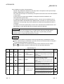
DANGER
Indicates that incorrect handling may cause hazardous conditions,
resulting in death or severe injury.
! CAUTION
Indicates that incorrect handling may cause hazardous conditions,
resulting in medium or slight personal injury or physical damage.
!
Note that the ! CAUTION level may lead to a serious consequence according to the circumstances.
Always follow the instructions of both levels because they are important to personal safety.
Please save this manual to make it accessible when required and always forward it to the end user.
[Design Precautions]
!
DANGER
• Install a safety circuit external to the PLC that keeps the entire system safe even when there are
problems with the external power supply or the PLC module. Otherwise, trouble could result
from erroneous output or erroneous operation.
(1) Outside the PLC, construct mechanical damage preventing interlock circuits such as
emergency stop, protective circuits, positioning upper and lower limits switches and
interlocking forward/reverse operations.
(2) When the PLC detects the following problems, it will stop calculation and turn off all output in
the case of (a). In the case of (b), it will stop calculation and hold or turn off all output
according to the parameter setting.
(a) The power supply module has over current protection equipment and over voltage
protection equipment.
(b) The PLC CPUs self-diagnostic functions, such as the watchdog timer error, detect
problems.
In addition, all output will be turned on when there are problems that the PLC CPU cannot
detect, such as in the I/O controller. Build a fail safe circuit exterior to the PLC that will make
sure the equipment operates safely at such times. Refer to " LOADING AND
INSTALLATION" in QCPU (Q Mode) User's Manual (Hardware Design/Maintenance and
Inspection) for example fail safe circuits.
(3) Output could be left on or off when there is trouble in the outputs module relay or transistor.
So build an external monitoring circuit that will monitor any single outputs that could cause
serious trouble.
A-1
A-1
[Design Precautions]
!
DANGER
• When overcurrent which exceeds the rating or caused by short-circuited load flows in the output
module for a long time, it may cause smoke or fire. To prevent this, configure an external safety
circuit, such as fuse.
• Build a circuit that turns on the external power supply when the PLC main module power is
turned on. If the external power supply is turned on first, it could result in erroneous output or
erroneous operation.
• When there are communication problems with the data link, refer to the corresponding data link
manual for the operating status of each station.
Not doing so could result in erroneous output or erroneous operation.
• When connecting a peripheral device to the CPU module or connecting a personal computer or
the like to the intelligent function module to exercise control (data change) on the running PLC,
configure up an interlock circuit in the sequence program to ensure that the whole system will
always operate safely.
Also before exercising other control (program change, operating status change (status control))
on the running PLC, read the manual carefully and fully confirm safety.
Especially for the above control on the remote PLC from an external device, an immediate
action may not be taken for PLC trouble due to a data communication fault.
In addition to configuring up the interlock circuit in the sequence program, corrective and other
actions to be taken as a system for the occurrence of a data communication fault should be
predetermined between the external device and PLC CPU.
!
CAUTION
• Do not bunch the control wires or communication cables with the main circuit or power wires, or
install them close to each other. They should be installed 100 mm (3.94 inch) or more from each
other.
Not doing so could result in noise that would cause erroneous operation.
• When controlling items like lamp load, heater or solenoid valve using an output module, large
current (approximately ten times greater than that present in normal circumstances) may flow
when the output is turned OFF to ON.
Take measures such as replacing the module with one having sufficient rated current.
A-2
A-2
[Installation Precautions]
!
CAUTION
• Use the PLC in an environment that meets the general specifications contained in this manual.
Using this PLC in an environment outside the range of the general specifications could result in
electric shock, fire, erroneous operation, and damage to or deterioration of the product.
• Hold down the module loading lever at the module bottom, and securely insert the module fixing
hook into the fixing hole in the base module. Incorrect loading of the module can cause a
malfunction, failure or drop.
When using the PLC in the environment of much vibration, tighten the module with a screw.
Tighten the screw in the specified torque range.
Undertightening can cause a drop, short circuit or malfunction.
Overtightening can cause a drop, short circuit or malfunction due to damage to the screw or
module.
• When installing more cables, be sure that the base module and the module connectors are
installed correctly.
After installation, check them for looseness.
Poor connections could cause an input or output failure.
• Securely load the memory card into the memory card loading connector.
After loading, check for lifting.
Lifting can cause a malfunction due to a contact fault.
• Completely turn off the external power supply before loading or unloading the module.
Not doing so could result in electric shock or damage to the product.
• Do not directly touch the module's conductive parts or electronic components.
Touching the conductive parts could cause an operation failure or give damage to the module.
[Wiring Precautions]
!
DANGER
• Completely turn off the external power supply when installing or placing wiring.
Not completely turning off all power could result in electric shock or damage to the product.
• When turning on the power supply or operating the module after installation or wiring work, be
sure that the module's terminal covers are correctly attached.
Not attaching the terminal cover could result in electric shock.
A-3
A-3
[Wiring Precautions]
!
CAUTION
• Be sure to ground the FG terminals and LG terminals to the protective ground conductor. Not
doing so could result in electric shock or erroneous operation.
• When wiring in the PLC, be sure that it is done correctly by checking the product's rated voltage
and the terminal layout.
Connecting a power supply that is different from the rating or incorrectly wiring the product could
result in fire or damage.
• External connections shall be crimped or pressure welded with the specified tools, or correctly
soldered.
Imperfect connections could result in short circuit, fires, or erroneous operation.
• Tighten the terminal screws with the specified torque.
If the terminal screws are loose, it could result in short circuits, fire, or erroneous operation.
Tightening the terminal screws too far may cause damages to the screws and/or the module,
resulting in fallout, short circuits, or malfunction.
• Be sure there are no foreign substances such as sawdust or wiring debris inside the module.
Such debris could cause fires, damage, or erroneous operation.
• The module has an ingress prevention label on its top to prevent foreign matter, such as wire
offcuts, from entering the module during wiring.
Do not peel this label during wiring.
Before starting system operation, be sure to peel this label because of heat dissipation.
[Startup and Maintenance precautions]
!
DANGER
• Do not touch the terminals while power is on.
Doing so could cause shock or erroneous operation.
• Correctly connect the battery. Also, do not charge, disassemble, heat, place in fire, short circuit,
or solder the battery.
Mishandling of battery can cause overheating or cracks which could result in injury and fires.
• Switch all phases of the external power supply off when cleaning the module or retightening the
terminal or module mounting screws. Not doing so could result in electric shock.
Undertightening of terminal screws can cause a short circuit or malfunction.
Overtightening of screws can cause damages to the screws and/or the module, resulting in
fallout, short circuits, or malfunction.
A-4
A-4
[Startup and Maintenance precautions]
!
CAUTION
• The online operations conducted for the CPU module being operated, connecting the peripheral
device (especially, when changing data or operation status), shall be conducted after the
manual has been carefully read and a sufficient check of safety has been conducted.
Operation mistakes could cause damage or problems with of the module.
• Do not disassemble or modify the modules.
Doing so could cause trouble, erroneous operation, injury, or fire.
• Use a cellular phone or PHS more than 25cm (9.85 inch) away from the PLC.
Not doing so can cause a malfunction.
• Switch all phases of the external power supply off before mounting or removing the module.
If you do not switch off the external power supply, it will cause failure or malfunction of the
module.
[Disposal Precautions]
!
CAUTION
• When disposing of this product, treat it as industrial waste.
A-5
A-5
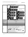
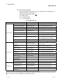
REVISIONS
The manual number is given on the bottom left of the back cover.
Print Date
Dec., 1999
Dec., 2000
* Manual Number
Revision
SH (NA) 080038-A First edition
SH (NA) 080038-B Add the Q33B type basic base unit and Q63B type extension base unit.
Change Chapter 11 (1) to (3) to Section 11.1 to 11.3.
Unify the name from the software package (GPP function, ladder logic
test tool function, GPPW, etc) to the product name (GX Developer, GX
Configurator).
Add the explanation of the following functions of which serial number's
top five digits were added in 02092 (02092
-A)
• Automatic writing to the standard ROM
• Forced ON/OFF correspondence for external I/O
• Remote password setting
• Increment of Q12HCPU and Q25HCPU standard RAM capacity
• MELSECNET/H remote I/O network correspondence
• Interrupt module (QI60) correspondence
Correction
Section 1.1, Section 2.1, 2.2, Chapter 3, Section 4.2, 4.2.1, 4.2.2, 4.2.3,
4.6, Section 5.2, 5.3, Section 6.1, 6.9.3, Section 7.3 (3) (4), 7.6.5, 7.8,
7.14, 7.18, 7.19.1, 7.20.1, Chapter 9, Section 10.2, 10.10, Section 11.3,
Appendix 1,2
Addition
Jun., 2001
Section 2.3, Section 4.1.3, 4.2.5, Section 5.4, 5.5.2, 5.6.2, Section 6.6,
6.6.2, 6.7, Section 7.6.3, 7.7.2, 7.7.3, 7.9.1, 7.9.3, 7.16, 7.17, 7.17.2,
7.20.1, Section 10.10
SH (NA) 080038-C The explanation of the multi PLC system added to the function version B
of the QCPU was added to Chapters 13 to 19.
General name for QCPU was changed to the High Performance model
QCPU.
The Q52B and Q55B extension base units and PC CPU module were
added.
Overall correction
Japanese Manual Version SH-080020-E
This manual confers no industrial property rights or any rights of any other kind, nor does it confer any patent
licenses. Mitsubishi Electric Corporation cannot be held responsible for any problems involving industrial property
rights which may occur as a result of using the contents noted in this manual.
1999 MITSUBISHI ELECTRIC CORPORATION
A-6
A-6
INTRODUCTION
Thank you for choosing the Mitsubishi MELSEC-Q Series of General Purpose Programmable Controllers.
Please read this manual carefully so that equipment is used to its optimum.
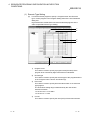
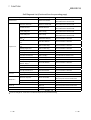
CONTENTS
SAFETY INSTRUCTIONS ...........................................................................................................................................A- 1
REVISIONS ....................................................................................................................................................................A- 6
CONTENTS....................................................................................................................................................................A- 7
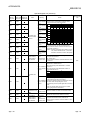
About Manuals............................................................................................................................................................... A-17
How to Use This Manual.............................................................................................................................................. A-18
About the Generic Terms and Abbreviations............................................................................................................. A-19
1. OVERVIEW
1 – 1 to 1 - 11
1.1 Features.....................................................................................................................................................................1- 2
1.2 Programs ...................................................................................................................................................................1- 5
1.3 Convenient Programming Devices and Instructions ............................................................................................1- 8
2. SYSTEM CONFIGURATION FOR SINGLE CPU SYSTEM
2- 1 to 2- 6
2.1 System Configuration..............................................................................................................................................2- 1
2.2 Precaution on System configuration.....................................................................................................................2- 4
2.3 Confirming the Serial No. and Function Versions................................................................................................2- 6
3. PERFORMANCE SPECIFICATION
3- 1 to 3- 3
4. SEQUENCE PROGRAM CONFIGURATION & EXECUTION CONDITIONS
4- 1 to 4-52
4.1 Sequence Program .................................................................................................................................................4- 1
4.1.1 Main routine program ........................................................................................................................ 4- 3
4.1.2 Sub-routine programs ....................................................................................................................... 4- 4
4.1.3 Interrupt programs............................................................................................................................. 4- 6
4.2 Program Execute Type ...........................................................................................................................................4-10
4.2.1 Initial execution type program........................................................................................................... 4-15
4.2.2 Scan execution type program ........................................................................................................... 4-17
4.2.3 Low-speed execution type program ................................................................................................. 4-19
4.2.4 Stand-by type program ..................................................................................................................... 4-25
4.2.5 Fixed scan execution type program.................................................................................................. 4-31
4.3 Operation processing ..............................................................................................................................................4-34
4.3.1 Initial processing................................................................................................................................ 4-34
4.3.2 I/O refresh (I/O module refresh processing)..................................................................................... 4-34
4.3.3 Automatic refresh of the intelligent function module ........................................................................ 4-35
4.3.4 END processing ................................................................................................................................ 4-35
4.4 RUN, STOP, PAUSE Operation Processing........................................................................................................4-36
4.5 Operation Processing during Momentary Power Failure....................................................................................4-37
A-7
A-7
4.6 Data Clear Processing ............................................................................................................................................4-38
4.7 Input/Output Processing and Response Lag .......................................................................................................4-39
4.7.1 Refresh mode.................................................................................................................................... 4-39
4.7.2 Direct mode ....................................................................................................................................... 4-42
4.8 Numeric Values which Can Be Used in Sequence Programs ...........................................................................4-44
4.8.1 BIN (Binary code) .............................................................................................................................. 4-46
4.8.2 HEX (Hexadecimal)........................................................................................................................... 4-47
4.8.3 BCD (Binary Coded Decimal) ........................................................................................................... 4-48
4.8.4 Real numbers (floating decimal point data)...................................................................................... 4-49
4.9 Character String Data..............................................................................................................................................4-52
5. ASSIGNMENT OF I/O NUMBERS
5- 1 to 5-18
5.1 Relationship Between the Number of Stages and Slots of the Extension Base Unit ......................................5- 1
5.2 Installing Extension Base Units and Setting the Number of Stages ..................................................................5- 2
5.3 Base Unit Assignment (Base Mode) ....................................................................................................................5- 3
5.4 What are I/O Numbers?..........................................................................................................................................5- 7
5.5 Concept of I/O Number Assignment......................................................................................................................5- 8
5.5.1 I/O numbers of main base unit and extension base units................................................................ 5- 8
5.5.2 Remote station I/O number............................................................................................................... 5-10
5.6 I/O Assignment by GX Developer..........................................................................................................................5-11
5.6.1 Purpose of I/O assignment by GX Developer .................................................................................. 5-11
5.6.2 Concept of I/O assignment using GX Developer ............................................................................. 5-12
5.7 Examples of I/O Number Assignment...................................................................................................................5-15
5.8 Checking the I/O Numbers .....................................................................................................................................5-18
6. HIGH PERFORMANCE MODEL QCPU FILES
6- 1 to 6-24
6.1 About the High Performance model QCPU's Memory........................................................................................6- 3
6.2 Program Memory.....................................................................................................................................................6- 6
6.3 About the Standard ROM .......................................................................................................................................6- 8
6.4 About the Standard RAM........................................................................................................................................6- 9
6.5 Memory Card ...........................................................................................................................................................6-11
6.6 Writing Data in the Standard ROM or on the Flash Card....................................................................................6-12
6.6.1 Writing Data in the standard ROM or on the flash card using the GX developer ........................... 6-12
6.6.2 Automatic writing in the standard ROM (automatically writing all data from the memory card to the
standard ROM) .............................................................................................................................. 6-14
6.7 Executing Standard ROM/Memory Card Programs (Boot Run)........................................................................6-17
6.8 Program File Configuration.....................................................................................................................................6-18
6.9 GX Developer File Operation and File Handling Precautions ............................................................................6-21
6.9.1 File operation..................................................................................................................................... 6-22
6.9.2 File handling precautions .................................................................................................................. 6-22
6.9.3 File size.............................................................................................................................................. 6-23
7. FUNCTION
7- 1 to 7-78
7.1 Function List .............................................................................................................................................................7- 1
7.2 Constant Scan..........................................................................................................................................................7- 2
7.3 Latch Functions........................................................................................................................................................7- 5
A-8
A-8
7.4 Setting the Output (Y) Status when Changing from STOP Status to RUN Status ..........................................7- 7
7.5 Clock Function .........................................................................................................................................................7- 9
7.6 Remote Operation ...................................................................................................................................................7-12
7.6.1 Remote RUN/STOP.......................................................................................................................... 7-12
7.6.2 Remote PAUSE................................................................................................................................. 7-15
7.6.3 Remote RESET................................................................................................................................. 7-17
7.6.4 Remote latch clear ............................................................................................................................ 7-18
7.6.5 Relationship of the remote operation and High Performance model QCPU RUN/STOP switch... 7-20
7.7 Selecting the Response Time of the Q series Compatible Input Module and Interrupt Module (I/O Response
Time).........................................................................................................................................................................7-21
7.7.1 Selecting the response time of the input module ............................................................................. 7-21
7.7.2 Selecting the response time of the high-speed input module.......................................................... 7-22
7.7.3 Selecting the response time of the interrupt module........................................................................ 7-23
7.8 Setting the Switches of the Intelligent Function Module......................................................................................7-24
7.9 Monitoring Function.................................................................................................................................................7-25
7.9.1 Monitor condition setting ................................................................................................................... 7-25
7.9.2 Monitoring test for local device ......................................................................................................... 7-29
7.9.3 Enforced ON/OFF for external I/O.................................................................................................... 7-31
7.10 Writing in Program during High Performance model QCPU RUN ..................................................................7-35
7.10.1 Writing data in the circuit mode during the RUN status ................................................................. 7-35
7.10.2 Writing a batch of files during RUN ................................................................................................ 7-38
7.11 Execution Time Measurement.............................................................................................................................7-40
7.11.1 Program monitor list ........................................................................................................................ 7-40
7.11.2 Interrupt program monitor list ......................................................................................................... 7-42
7.11.3 Scan time measurement................................................................................................................. 7-43
7.12 Sampling Trace Function......................................................................................................................................7-45
7.13 Debug Function with Multiple Users....................................................................................................................7-54
7.13.1 Multiple-user monitoring function.................................................................................................... 7-55
7.13.2 Multiple-user RUN write function .................................................................................................... 7-56
7.14 Watchdog Timer (WDT)........................................................................................................................................7-58
7.15 Self-Diagnosis Function........................................................................................................................................7-60
7.15.1 Interrupt due to error occurrence.................................................................................................... 7-63
7.15.2 LED display when error occurs....................................................................................................... 7-63
7.15.3 Cancel error..................................................................................................................................... 7-64
7.16 Failure History........................................................................................................................................................7-65
7.17 System Protect.......................................................................................................................................................7-66
7.17.1 Password registration...................................................................................................................... 7-66
7.17.2 Remote password ........................................................................................................................... 7-68
7.18 Monitoring High Performance model QCPU System Status from GX Developer (System Monitor) ..........7-71
7.19 LED Display............................................................................................................................................................7-75
7.19.1 LED display ..................................................................................................................................... 7-75
7.19.2 Priority setting.................................................................................................................................. 7-77.
A-9
A-9
8. COMMUNICATION WITH INTELLIGENT FUNCTION MODULE/SPECIAL FUNCTION MODULE
8- 1 to 8- 9
8.1 Communication Between High Performance model QCPU and Q-series Intelligent Function Modules......88.1.1 Initial setting and automatic refresh setting using GX Configurator ................................................ 88.1.2 Communication using device initial value......................................................................................... 88.1.3 Communication using FROM/TO instruction ................................................................................... 88.1.4 Communication using the intelligent function module device.......................................................... 88.1.5 Communication using the instructions dedicated for intelligent function modules.......................... 88.2 Request from Intelligent Function Module to High Performance model QCPU ...............................................88.2.1 Interrupt from the intelligent function module ................................................................................... 88.3 Communication Between High Performance model QCPU and AnS-Series Special Function Modules ....88.3.1 Communication using device initial value......................................................................................... 88.3.2 Communication using FROM/TO instruction ................................................................................... 78.3.3 Communication using the intelligent function module device.......................................................... 78.3.4 Effects of quicker access to the special function module and countermeasures against them ..... 79. PARAMETER LIST
10. DEVICES
1
2
3
4
4
5
6
6
7
7
8
8
9
9- 1 to 9- 6
10- 1 to 10-71
10.1 Device List............................................................................................................................................................10- 1
10.2 Internal User Devices..........................................................................................................................................10- 3
10.2.1 Inputs (X) ....................................................................................................................................... 10- 5
10.2.2 Outputs (Y) .................................................................................................................................... 10- 8
10.2.3 Internal relays (M) ......................................................................................................................... 10-10
10.2.4 Latch relays (L).............................................................................................................................. 10-11
10.2.5 Anunciators (F).............................................................................................................................. 10-12
10.2.6 Edge relay (V)................................................................................................................................ 10-16
10.2.7 Link relays (B)................................................................................................................................ 10-17
10.2.8 Special link relays (SB) ................................................................................................................. 10-18
10.2.9 Step relays (S)............................................................................................................................... 10-18
10.2.10 Timers (T) .................................................................................................................................... 10-19
10.2.11 Counters (C)................................................................................................................................ 10-24
10.2.12 Data registers (D) ........................................................................................................................ 10-28
10.2.13 Link registers (W) ........................................................................................................................ 10-29
10.2.14 Special link registers (SW).......................................................................................................... 10-30
10.3 Internal System Devices.....................................................................................................................................10-31
10.3.1 Function devices (FX, FY, FD) ..................................................................................................... 10-31
10.3.2 Special relays (SM) ....................................................................................................................... 10-33
10.3.3 Special registers (SD) ................................................................................................................... 10-34
10.4 Link Direct Devices (J \ ) ...............................................................................................................................10-35
10.5 Intelligent Function Module Devices (U \G ) ...............................................................................................10-38
A - 10
A - 10
10.6 Index Registers (Z)..............................................................................................................................................10-39
10.6.1 Switching between scan execution type programs and low-speed execution type programs ... 10-40
10.6.2 Switching between scan/low-speed execution programs and interrupt/fixed scan execution type
programs ...................................................................................................................................... 10-41
10.7 File Registers (R).................................................................................................................................................10-43
10.7.1 File register capacity ..................................................................................................................... 10-44
10.7.2 Differences in memory card access method by memory card type ............................................ 10-44
10.7.3 Registering the file registers ......................................................................................................... 10-45
10.7.4 File register designation method................................................................................................... 10-49
10.7.5 Precautions in using file registers ................................................................................................. 10-50
10.8 Nesting (N) ...........................................................................................................................................................10-52
10.9 Pointers.................................................................................................................................................................10-53
10.9.1 Local pointers ................................................................................................................................ 10-53
10.9.2 Common pointers.......................................................................................................................... 10-54
10.10 Interrupt Pointers (I)...........................................................................................................................................10-56
10.11 Other Devices ....................................................................................................................................................10-58
10.11.1 SFC block device (BL) ................................................................................................................ 10-58
10.11.2 SFC transition device (TR) ......................................................................................................... 10-58
10.11.3 Network No. designation device (J)............................................................................................ 10-58
10.11.4 I/O No. designation device (U).................................................................................................... 10-59
10.11.5 Macro instruction argument device (VD).................................................................................... 10-60
10.12 Constants ...........................................................................................................................................................10-61
10.12.1 Decimal constants (K)................................................................................................................. 10-61
10.12.2 Hexadecimal constants (H)......................................................................................................... 10-61
10.12.3 Real numbers (E) ........................................................................................................................ 10-62
10.12.4 Character string ( " " )................................................................................................................ 10-62
10.13 Convenient Uses for Devices...........................................................................................................................10-63
10.13.1 Global devices & local devices ................................................................................................... 10-63
10.13.2 Device initial values..................................................................................................................... 10-69
11 HIGH PERFORMANCE MODEL QCPU PROCESSING TIME
11- 1 to 11- 4
11.1 Reading High Performance model QCPU's Scan Time................................................................................11- 1
11.2 Factors Responsible for Extended Scan Time ...............................................................................................11- 2
11.3 Factors Responsible for Shortened Scan Time..............................................................................................11- 4
12 PROCEDURE FOR WRITING PROGRAMS TO HIGH PERFORMANCE MODEL QCPU
12- 1 to-12-
12.1 Writing Procedure for 1 Program......................................................................................................................1212.1.1 Items to consider when creating one program............................................................................ 1212.1.2 Procedure for writing programs to the High Performance model QCPU ................................... 1212.2 Procedure for Multiple Programs......................................................................................................................1212.2.1 Items to consider when creating multiple programs ................................................................... 1212.2.2 Procedure for writing programs to the High Performance model QCPU ................................... 12-
A - 11
A - 11
1
2
2
5
5
6
13 OUTLINE OF MULTIPLE PLC SYSTEMS
13- 1 to 13- 6
13.1 Features...............................................................................................................................................................13- 1
13.2 Outline of Multiple PLC Systems ......................................................................................................................13- 3
13.3 Differences with Single CPU Systems ............................................................................................................13- 5
14 SYSTEM CONFIGURATION OF MULTIPLE PLC SYSTEMS
14- 1 to 14- 20
14.1 System Configuration.........................................................................................................................................14- 1
14.2 Precautions During Multiple PLC System Configuration ...............................................................................14- 1
14.2.1 Function versions of High Performance model QCPU , motion CPUs and PC CPU module that
can be sued, and their mounting positions ................................................................................. 14- 4
14.2.2 Precautions when using Q series corresponding I/O modules and intelligent function modules14- 4
14.2.3 Limitations when mounting AnS series corresponding I/O modules and special function
modules .................................................................................................................................................... 14- 9
14.2.4 Modules that have mounting restrictions..................................................................................... 14-11
14.2.5 Usable GX Developers and GX Configurators............................................................................ 14-12
14.2.6 Parameters that enable the use of multiple PLC systems.......................................................... 14-13
14.2.7 Resetting the multiple PLC system ............................................................................................. 14-17
14.2.8 Processing when High Performance model QCPU stop errors occur ....................................... 14-18
14.2.9 Reducing the time required for multiple PLC system processing............................................... 14-20
15 ALLOCATING MULTIPLE PLC SYSTEM I/O NUMBERS
15- 1 to 15- 3
15.1 Concept behind Allocating I/O Numbers..........................................................................................................1515.1.1 I/O modules and intelligent function module I/O numbers.......................................................... 1515.1.2 I/O number of High Performance model QCPU, Motion CPU and PC CPU module ................ 1515.2. Purpose of PC Parameter I/O Allocations with the GX Developer ..............................................................1516 COMMUNICATION BETWEEN CPU MODULES IN MULTIPLE PLC SYSTEM
1
1
2
3
16- 1 t o 16-15
16.1 Automatic Refresh of Common CPU Memory................................................................................................16- 2
16.2 Communication with Multiple PLC Commands and Intelligent Function Module Devices................... 16- 9
16.3 Interactive Communications between The High Performance model QCPU and Motion CPU ...............16-11
16.3.1 Control instructions from the High Performance model QCPU to the motion CPU................... 16-11
16.3.2 Reading and writing device data ................................................................................................. 16-12
16.4 Common CPU Memory.....................................................................................................................................16-13
17 COMMUNICATIONS BETWEEN THE MULTIPLE PLC SYSTEM'S I/O MODULES AND
INTELLIGENT FUNCTION MODULES
17- 1 to 17- 5
17.1 Range of Control PLC Communications..........................................................................................................17- 1
17.2 Range of Non-control PLC Communications..................................................................................................17- 1
A - 12
A - 12
18 PROCESSING TIME FOR MULTIPLE PLC SYSTEM HIGH PERFORMANCE MODEL
QCPUs
18- 1 to 18- 3
18.1 Concept behind CPU Scanning Time..............................................................................................................18- 1
18.2 Factor to Prolong the Scan Time......................................................................................................................18- 2
19 STARTING UP THE MULTIPLE PLC SYSTEM
19- 1 to 19- 9
19.1 Flow-chart for Starting Up the Multiple PLC System ......................................................................................1919.2 Setting Up the Multiple PLC System Parameters (Multiple PLC Settings, Control PLC Settings)............1919.2.1 System configuration.................................................................................................................... 1919.2.2 Creating new systems.................................................................................................................. 1919.2.3 Using existing preset multiple PLC settings and I/O allocations ................................................................19APPENDICES
1
3
3
4
7
App- 1 to App-58
APPENDIX 1 Special Relay List.............................................................................................................................. App- 1
APPENDIX 2 Special Register List.........................................................................................................................App-22
APPENDIX 3 List of Interrupt Pointer Nos. & Interrupt Factors ...........................................................................App-58
INDEX
A - 13
Index -1 to Index 3
A - 13
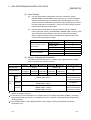
(Related manual).........................QCPU (Q Mode) User's Manual (Hardware Design/Maintenance and Inspection)
CONTENTS
1. OVERVIEW
1.1 Overview
1.2 Features
2. SYSTEM CONFIGURATION
2.1 System Configuration
2.2 Precaution on System Configuration
2.3 Comfirming Serial Number
3. GENERAL SPECIFICATIONS
4. HARDWARE SPECIFICATION OF THE CPU MODULE
4.1 Performance Specification
4.2 Part Names and Settings
4.3 Switch Operation After Writing in Program
4.4 Latch Clear Operation
4.5 Automatic Writing Operation in the Standard RAM
5. POWER SUPPLY MODULE
5.1 Specification
5.1.1 Power supply module specifications
5.1.2 Selecting the power supply module
5.1.3 Precaution when connecting the uninterruptive power supply
5.2 Names of Parts and Settings
6. BASE UNIT AND EXTENSION CABLE
6.1 Base Unit Specification Table
6.2 Extension Cable Specification Table
6.3 The Names of The Parts of The Base Unit
6.4 Setting the Extension Base Unit
6.5 I/O Allocations
A - 14
A - 14
7. MEMORY CARD AND BATTERY
7.1 Memory Card Specifications
7.2 Battery Specifications (For CPU Module and SRAM Card)
7.3 Handling the Memory Card
7.4 The Names of The Parts of The Memory Card
7.5 Memory Card Loading/Unloading Procedures
7.6 Installation of Battery (for CPU Module and Memory Card)
8. EMC AND LOW-VOLTAGE DIRECTIVES
8.1 Requirements for conformance to EMC Directive
8.1.1 Standards applicable to the EMC Directive
8.1.2 Installation instructions for EMC Directive
8.1.3 Cables
8.1.4 Power supply module
8.1.5 When using Q1AS6 B type base unit
8.1.6 Others
8.2 Requirement to Conform to the Low-Voltage Directive
8.2.1 Standard applied for MELSEC-Q series
8.2.2 MELSEC-Q series PLC selection
8.2.3 Power supply
8.2.4 Control box
8.2.5 Grounding
8.2.6 External wiring
9. LOADING AND INSTALLATION
9.1 General Safety Requirements
9.2 Calculating Heat Generation by PLC
9.3 Module Installation
9.3.1 Precaution on installation
9.3.2 Instructions for mounting the base unit
9.3.3 Installation and removal of module
9.4 Setting the Extension Number of the Extension Base Unit
9.5 Connection and Disconnection of Extension Cable
9.6 Wiring
9.6.1 The precautions on the wiring
9.6.2 Connecting to the power supply module
10. MAINTENANCE AND INSPECTION
10.1 Daily Inspection
10.2 Periodic Inspection
10.3 Battery Replacement
10.3.1 Battery service life
10.3.2 Battery replacement procedure
A - 15
A - 15
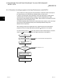
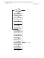
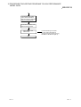
11. TROUBLESHOOTING
11.1 Troubleshooting Basics
11.2 Troubleshooting
11.2.1 Troubleshooting flowchart
11.2.2 Flowchart for when "MODE" LED is not turned on
11.2.3 Flowchart for when "MODE" LED is flashing
11.2.4 Flowchart for when "POWER" LED is turned off
11.2.5 Flowchart for when the "RUN" LED is turned off
11.2.6 When the "RUN" LED is flashing
11.2.7 Flowchart for when "ERROR" LED is on/flashing
11.2.8 When "USER" LED is turned on
11.2.9 When "BAT.ARM" LED is turned on
11.2.10 Flowchart for when "BOOT LED" is flashing
11.2.11 Flowchart for when the output module LED does not turn on
11.2.12 Flowchart for when output load of output module does not turn on
11.2.13 Flowchart for when unable to read a program
11.2.14 Flowchart for when unable to write a program
11.2.15 Flowchart for when it is unable to perform boot operation from memory card
11.2.16 Flowchart for when UNIT VERIFY ERR. occurs
11.2.17 Flowchart for when CONTROL BUS ERR. occurs
11.3 Error Code List
11.3.1 Procedure for reading error codes
11.3.2 Error code list
11.4 Canceling of Errors
11.5 I/O Module Troubleshooting
11.5.1 Input circuit troubleshooting
11.6 Special Relay List
11.7 Special Register List
APPENDICES
APPENDIX 1 Error Code Return to Origin During General Data Processing
APPENDIX 1.1 Error code overall explanation
APPENDIX 1.2 Description of the errors of the error codes (4000H to 4FFFH)
APPENDIX 2 External Dimensions Diagram
APPENDIX 2.1 CPU module
APPENDIX 2.2 Power supply module
APPENDIX 2.3 Main base unit
APPENDIX 2.4 Extension base unit
INDEX
A - 16
A - 16
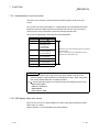
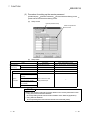
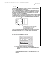
About Manuals
The following manuals are also related to this product.
In necessary, order them by quoting the details in the tables below.
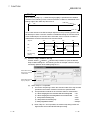
Related Manuals
Manual Number
(Model Code)
Manual Name
QCPU (Q Mode) User's Manual (Hardware Design, Maintenance and Inspection)
This manual provides the specifications of the CPU modules, power supply modules, base modules,
extension cables, memory cards and others.
SH-080037
(13JL97)
(Option)
QCPU (Q Mode)/QnACPU Programming Manual (Common Instructions)
Describes how to use the sequence instructions, basic instructions, advanced instructions, and microcomputer programs.
(Option)
QCPU (Q Mode)/QnACPU Programming Manual (PID Control Instructions)
This manual describes the dedicated instructions used to exercise PID control.
SH-080039
(13JF58)
(Option)
SH-080040
(13JF59)
QCPU (Q Mode)/QnACPU Programming Manual (SFC)
This manual explains the system configuration, performance specifications, functions, programming,
debugging, error codes and others of MELSAP3.
A - 17
SH-080041
(13JF60)
(Option)
A - 17
How to Use This Manual
This manual is prepared for users to understand memory map, functions, programs and devices of the CPU
module when you use MELSEC-Q series sequencers.
The manual is classified roughly into three sections as shown below.
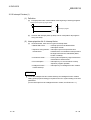
(1) Chapters 1 and 2
Describe the outline of the CPU module and the system
configuration. The feature of CPU module and the basics
of the system configuration of CPU are described.
(2) Chapters 3 to 6
Describe the performance specifications, executable
program, I/O No. and memory of the CPU module.
(3) Chapter 7
Describes the functions of the CPU modules.
(4) Chapter 8
Describes communication with intelligent function modules.
(5) Chapters 9 and 10
Describe parameters and devices used in the CPU
modules.
(6) Chapter 11
Describes the CPU module processing time.
(7) Chapter 12
Describes the procedure for writing parameters and
programs created at the GX Developer to the CPU module.
(8) Chapters 13 to 19
Describes an overview of the multiple PLC system, the
system configuration, the I/O numbers, communications
between CPU modules, and communications between I/O
modules and intelligent function modules.
REMARK
This manual does not explain the functions of power supply modules, base units,
extension cables, memory cards and batteries of QCPU.
For these functions, refer to the manual shown below.
• QCPU (Q Mode) User's Manual (Hardware Design, Maintenance and Inspection)
A - 18
A - 18
About the Generic Terms and Abbreviations
The following abbreviations and general names for Q02CPU, Q02HCPU, Q06HCPU Q12HCPU, and
Q25HCPU are used in the manual.
Description
General name for Q02CPU, Q02HCPU, Q06HCPU Q12HCPU and Q25HCPU
High Performance model QCPU
modules.
General name for Q02CPU.
QnCPU
General name for Q02HCPU, Q06HCPU Q12HCPU, and Q25HCPU
QnHCPU
Abbreviation for Mitsubishi MELSEC-Q Series General Purpose Programmable Logic
Q Series
Controller.
Abbreviation for small types of Mitsubishi MELSEC-A Series General Purpose
AnS Series
Programmable Logic Controller.
General product name for SWnD5C-GPPW-E, SWnD5C-GPPW-A-E, SWnD5CGX Developer
GPPW-V-E, SWnD5C-GPPW-VA-E.
For QCPU, version 4 or later can be used.
General name for Q33B, Q35B, Q38B, Q312B type main base unit with Q Series
Main base unit
power module, I/O module, intelligent function module attachable.
General name for Q63B, Q65B, Q68B and Q612B type extension base unit with Q
Q6 B
Series power module, I/O module, intelligent function module attachable.
General name for QA1S65B and QA1S68B type extension base unit with AnS Series
QA1S6 B
power module, I/O module, special function module attachable.
General name for Q6 B and QA1S6 B.
Extension base unit
General name for Basic base unit and extension base unit.
Base unit
Abbreviation for Q2MEM-1MBS type SRAM card.
SRAM card
General name for Q2MEM-2MBS and Q2MEM-4MBS type Flash card.
Flash card
General name for Q2MEM-8MBS, Q2MEM-16MBS and Q2MEM-32MBS type ATA
ATA card
card.
General name for SRAM card, Flash card and ATA card.
Memory card
General name for Q61P-A1, Q61P-A2, A1S61PN, A1S62P and A1S63P type power
Power supply module
supply module.
General name for battery for Q6BAT type CPU module and Q2MEM-BAT type SRAM
Battery
card.
General name for QC06B, QC12B, QC30B, QC50B, QC100B type extension cable.
Extension cable
General name for Q52B and Q55B that accept the Q series I/O and intelligent function
Q5 B
modules.
High Performance model QCPU/motion CPU that controls any of the I/O and
intelligent function modules loaded on the main or extension base unit. For example,
Control CPU
when the module loaded on slot 3 is controlled by the CPU No. 2, the CPU No. 2 is
the control CPU of the module on slot 3.
I/O or intelligent function module other than the controlled module. For example, when
Non-controlled module
the module loaded on slot 3 is controlled by the CPU No. 2, the module on slot 3 is
(Non-group module)
the non-controlled module of the CPU Nos. 1, 3 and 4.
I/O or intelligent function module controlled by the control CPU. For example, when
Controlled module
the module loaded on slot 3 is controlled by the CPU No. 2, the module on slot 3 is
the controlled module of the CPU No. 2.
Numbers assigned to differentiate between the High Performance model QCPU and
motion CPU loaded in a multi PLC system. The CPU on the CPU slot is the CPU No.
CPU numbers
1, the one on slot 0 is the CPU No. 2, the one on slot 1 is the CPU No. 3, and the one
on slot 2 is the CPU No. 4.
System loaded with the High Performance model QCPU on the CPU slot to exercise
Single PLC system
control.
MELSEC-Q series compatible PC CPU module
PC CPU module
High Performance model QCPUs and/or motion CPUs other than the control CPU.
Non-control CPUs
For example, when the module loaded on slot 3 is controlled by the CPU No. 2, the
CPU Nos. 1, 3 and 4 are the non-control CPUs of the module on slot 3.
System loaded with up to four High Performance model QCPU, motion CPU and PC
Multi PLC system
CPU modules on the main base unit to exercise control.
Generic Term/Abbreviation
A - 19
A - 19
1 OVERVIEW
MELSEC-Q
1 OVERVIEW
1
This Manual describes the function, program, and device of the High Performance
model QCPU.
Refer to the following functions for details on power supply modules, base units,
extension cables, memory cards, battery specifications and other information.
High Performance model QCPU (Q mode) User's Manual (Hardware Design,
Maintenance and Inspections)
(1) Additional functions with products whose first 5 digits of the serial
number are "02092"
The following functions have been added to the High Performance model QCPU
products whose first 5 digits of the serial number are "02092."
• Automatic write to standard ROM (see Section 6.6.2)
• External I/O can be turned ON/OFF forcibly (see Section 7.9.3)
• Remote password setting (see Section 7.19)
• Q12HCPU, Q25HCPU's increased standard RAM capacity (see Chapter 3,
Section 6.4)
• MELSECNET/H remote I/O network compatibility (see Section 1.1)
• Interrupt module (QI60) compatibility (See Section 7.7.3.)
(2) Additional functions with products whose function version is B
The following functions have been added to the High Performance Model QCPU
products whose function version is B.
• Applicability to the multiple-PLC system (see Chapters 13 to 19)
(3) Additional functions with products whose first 5 digits of the serial
number are "03051"
• Installation of PC CPU unit into the multiple-PLC system (see Chapters 13 to
19)
POINT
(1) When using a QCPU with the first five digits of the serial number being "02091"
or earlier, skip the pages explaining the functions added to those with serial
numbers starting with "02092."
(2) When a multiple PLC system is not in use, skip Chapters 13 to 19.
(2) When a PC CPU unit is not in use, skip Chapters 13 to 19.
(3) Refer to Section 2.3 to confirm High Performance model QCPU serial numbers
and function versions
REMARK
High Performance model QCPU is the generic term for the Q02CPU, Q02HCPU,
Q06HCPU, Q12HCPU and Q25HCPU general-purpose PLC. Q02CPU, Q02HCPU,
Q06HCPU, Q12HCPU and Q25HCPU are also mentioned when providing individual
explanations for each module.
1-1
1-1
1 OVERVIEW
MELSEC-Q
1.2 Features
1
High Performance model QCPU has the following new features:
(1) Controllable multiple I/O points
All High Performance model QCPUs support 4096 points (X/YO to FFF) as the
number of actual I/O points capable of getting access to the I/O module installed
on the base unit.
They also support 8192 points max. (X/YO to 1FFF) as the number of I/O
devices which can be used in the remote I/O stations such as MELSECNET/H
remote I/O NET, CC-Link data link and MELSECNET/MINI-S3 data link.
(2) Lineup according to program capacity
The optimum CPU module for the program capacity to be used can be selected.
Q02CPU, Q02HCPU : 28k step
Q06HCPU
: 60k step
Q12HCPU
: 124k step
Q25HCPU
: 252k step
(3) Realised high speed processing
Depending on the type of the sequencer, high-speed processing has been
realized.(Example: when LD instruction is used)
Q02CPU
: 0.079µs
Q02HCPU, Q06HCPU, Q12HCPU, Q25HCPU : 0.034µs
In addition, an access to the intelligent function module or an increase in speed
of the link refresh of the network have been realized by the connection system
(System bus connection) of the newly developed base unit.
Access to the intelligent function module : 20µs /word (approx. 7 times) 1
MELSECNET/H link refresh processing : 4.6ms/8k word (approx. 4.3 times) 1
1: Where Q02HCPU is compared with Q2ASHCPU-S1.
(4) Increase in debugging efficiency through high-speed
communication with GX Developer
In the High Performance model QCPU, a time required for writing/reading of a
program or monitoring has been reduced through the high speed communication
at a speed of 115.2kbps max. by the RS-232, and a communication time
efficiency at the time of debugging has been increased.
In the Q02HCPU, Q06HCPU, Q12HCPU, and Q25HCPU, a high-speed
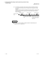
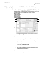
communication at a speed of 12Mbps is allowed through the USB.
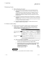
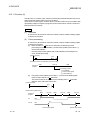
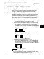
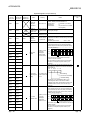
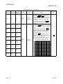
26k step program transfer time
Q25HCPU(USB)
Q25HCPU(RS-232)
Q2ASHCPU
A2USHCPU-S1
12
30
86
94
0 10 20 30 40 50 60 70 80 90 100 (Unit:s)
(5) AnS series I/O module or special function module are available.
For Q series, if an appropriate module is not available, the AnS series I/O
module or special function module can also be used for the High Performance
model QCPU through the use of the QA1S65B/QA1S68B extension base unit.
1-2
1-2
1 OVERVIEW
MELSEC-Q
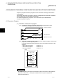
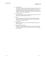
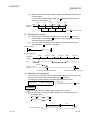
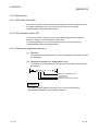
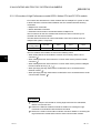
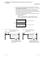
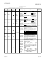
(6) Saved space by a reduction in size
The installation space for Q series has been reduced by approx. 60 % of the
space for AnS series.
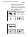
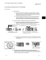
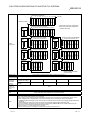
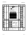
Comparison of installation space
1SX10
98mm
(3.86
inch)
1SY50
1SX41
1SY41
1SX81
1SY81
1SX42
1SY42
PULL
5 Slot Basic Base Unit 245mm(9.65inch)
(depth:98mm(3.86inch))
8 Slot Basic Base Unit 328mm(12.92inch)
8 Slot Basic Base Unit 439mm(17.30inch)
(7) Connection of up to seven extension base units.
(a) The High Performance model QCPU can connect to seven extension base
units (eight base units including the main) and accept up to 64 modules.
(b) The overall distance of the extension cables is up to 13.2m to ensure high
degree of extension base unit arrangement.
(8) Memory extension by memory card
The High Performance model QCPU is provided with a memory card installation
connector to which a memory card of 32 Mbyte max. can be connected (32 Mbite
is available when a ATA card is used).
When a memory card of large capacity is installed, a large capacity of file can be
controlled, comments to all data devices can be set up, and the programs in the
past can be stored in the memory as they are in the form of the corrected
histories.
If a memory card is not installed, a program can be stored onto the standard
ROM built in the High Performance model QCPU, and 32k/128k points of file
registers can be handled by the standard RAM.
(9) Data can be written automatically to standard ROM
You need not use GX Developer to write parameters/programs on a memory
card to the standard ROM of the High Performance model QCPU.
When the standard ROM is used to perform ROM operation, you can load a
memory card into the High Performance model QCPU and write
parameters/programs on the memory card to the standard ROM. Hence, you
need not carry GX Developer (personal computer) to rewrite the
parameters/programs.
REMARK
: File registers as big as 128k points can be handled by the Q12HCPU and
Q25HCPU whose function version is B.
The total size of file registers of the Q02CPU, Q02HCPU, Q06HCPU, and
Q12HCPU and Q25HCPU whose function version is A is 32k points.
1-3
1-3
1 OVERVIEW
MELSEC-Q
(10) External I/O can be turned ON/OFF forcibly
If the High Performance model QCPU is in the RUN mode, you can operate GX
Developer to turn external inputs/outputs ON/OFF forcibly, independently of the
program execution status.
You need not put the High Performance model QCPU in the STOP mode to
perform wiring/operation tests by forced ON/OFF of outputs.
(11) Remote password can be set
When access to an Ethernet module or serial communication module is made
externally, whether access to the High Performance model QCPU can be made
or not can be selected with a remote password.
(12) Remote I/O network of MELSECNET/H can be configured
You can load the remote master station of the MELSECNET/H to configure an
MELSECNET/H remote I/O system.
(13) Compatibility with PC CPU module in multi PLC system
configuration
A multiple-PLC system can be configured by the High Performance model
QCPU, motion CPU and PC CPU modules.
(14) Ease of handling CC-Link system
When using one master module of a CC-Link system, you can control I/O signals
to/from up to 64 remote I/O remote I/O stations without parameters.
Also, you can control the remote I/O stations as if you were controlling the I/O
modules on the base units.
(15) File password for protection against illegal access operation
Setting of the program access level (read disable, write disable) with a file
password prevents program file/device initial value file/device comment file from
being changed by illegal access.
REMARK
• Features (9) to (12) are functions added to the High Performance model QCPU
whose serial number is "02092" or later in its upper 5 digits.
• The remote password facility can be executed when the Ethernet module or serial
communication module of function version B and GX Developer Version 6 or later
are used.
• In addition to the remote password, there are the following protection facilities for
the High Performance model QCPU.
Protection of the whole CPU by making system settings of the High Performance
model QCPU
Protection of the memory card by setting the write protect switch of the memory card
File-by-file protection using password
• The MELSECNET/H remote I/O network facility can be executed when the
MELSECNET/H network module of function version B and GX Developer (Version
6 or later) are used.
• The feature in (13) is the function added to the High Performance mode QCPU
whose upper five digits of the serial No. are "03051".
1-4
1-4
1 OVERVIEW
MELSEC-Q
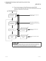
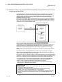
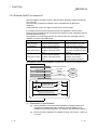
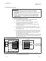
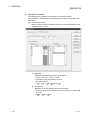
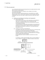
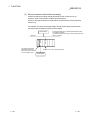
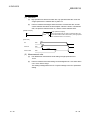
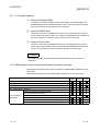
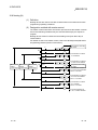
1.2 Programs
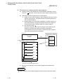
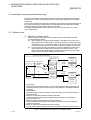
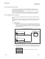
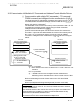
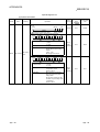
(1) Program management by memory card is possible
(a)
Programs created at GX Developer can be stored in the QCPU's program
memory, standard ROM or memory card.
QCPU
Program memory
Parameter
Program
Standard ROM
1
Memory
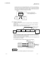
card
RAM
Parameter
Parameter
Program
Program
File register
(only read process
is enabled)
File register
Standard RAM
2
File register
(32k word)
ROM
Parameter
Program
File register
When flash card
is used, only read
process is enabled
1: The standard ROM is used when parameters and programs are written
to ROM.
2: The standard RAM is used when access to the file register need to
speed up.
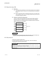
(b)
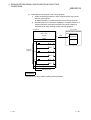
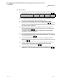
The QCPU processes programs which are stored in the program memory.
QCPU
Program memory
Parameter
Execution of program
in program memory
Program
1-5
1-5
1 OVERVIEW
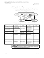
MELSEC-Q
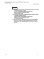
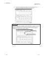
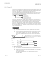
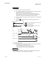
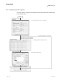
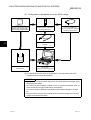
Programs stored in the standard ROM/memory card are executed after they
are booted to (read to) the QCPU program memory. (Programs to be booted
to the QCPU are designated by parameter settings, and the parameter drive
is designated by a DIP switch setting at the QCPU.)
QCPU
Program memory
Execution of program booted
from the standard ROM or memory
card to the program memory.
Parameter
Program
Boot
Standard ROM
Memory card
Parameter
Parameter
Program
Program
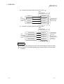
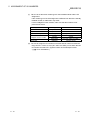
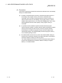
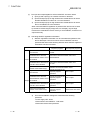
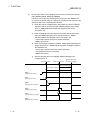
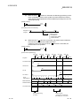
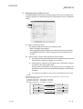
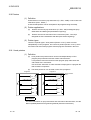
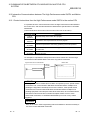
(2) Program construction
Programs are stored in a file format in the program memory, standard ROM or
memory card.
Multiple programs can therefore be stored in the program memory, standard
ROM or memory card by using different file names.
File name: ABC
Parameter
GX
Developer
Program
File name: ABC
Device
comments
Multiple program writing
is possible by using
different file names.
File name: DEF
Program
QCPU
Writing from GX Developer to QCPU
This format permits the program creation operation to be split among several
designers, and allows program management and maintenance to be carried out
according to the process or function in question.
Moreover, revision and debugging is required only at the relevant programs when
the specifications are changed.
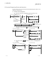
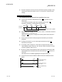
(a)
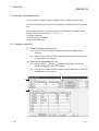
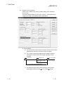
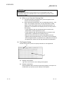
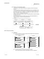
Example of program creation split among several designers:
QCPU
Program memory
/ Standard ROM / Memory card
Designer A
Program A
Designer B
Program B
Designer C
Program C
Programs A to C
are executed in
sequence. 1
REMARK
1: See Section 4.2 for details regarding the execution sequence.
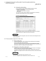
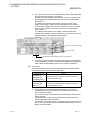
1-6
1-6
1 OVERVIEW
MELSEC-Q
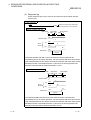
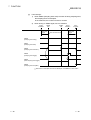
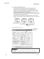
(b)
Example of programs split according to process:
1
QCPU
Program memory
/ Standard ROM / Memory card
Program A
Ship in
Split
according
to process
content
(c)
Program B
Manufacturing
Assembly
Program C
Ship out
Program D
Programs A to D
are executed in
sequence. 2
Example of programs split according to function:
QCPU
Program memory
/ Standard ROM / Memory card
Split
according
to function
content
Initial processing
Program A
Main processing
Program B
Communication processing
Program C
Error processing
Program D
The execution
sequence and
execution
conditions can
be set to conform
to programs
A to D. 2
REMARK
1: Programs split according to process can be further split according to function.
2: See Section 4.2 for details regarding the execution sequence and execution
conditions.
1-7
1-7
1 OVERVIEW
MELSEC-Q
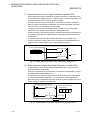
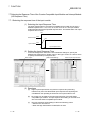
1.3 Convenient Programming Devices and Instructions
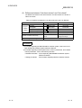
The QCPU features devices and instructions which facilitate program creation. A few
of these are described below.
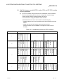
(1) Flexible device designation
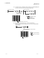
(a)
Word device bits can be designated to serve as contacts or coils.
[For the case of QCPU]
Bit designation of
word device
X0 D0.5
D0.A
The 1/0 status
of b5 of D0 is used
as ON/OFF data.
[For the case of AnS]
X0
MOV
D0
K4M0
M5
Switches b10
of D0 ON and
OFF (1/0).
M10
MOV K4M0
D0
: D0.5
b15 b14 b13 b12 b11b10 b9 b8 b7 b6 b5 b4 b3 b2 b1 b0
D0
1/0
1/0
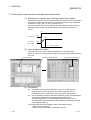
(b)
Bit designation
Word device designation
Direct processing in 1-point units is possible within a program simply by
using direct access inputs (DX ) and direct access outputs (DY ).
[For the case of QCPU]
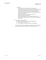
[For the case of AnS]
Direct access input
M0 DX10
M9036
SET M9052
DY100
(Always ON)
M9036
Output to output
module at
instruction execution
Read from input
module at
instruction
execution
M0
SEG K1X10 K1B0
(X10 to X13 refresh)
X10
Y100
M9036
SEG K1Y100 K1B0
(Y100 to Y103 refresh)
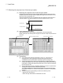
(c)
Differential contacts (
pulses.
/
[For the case of QCPU]
) eliminate the need for converting inputs to
[For the case of AnS]
Differential contact
X0
X1
X0
Y100
PLS
M0
Y100
M0
X1
Y100
ON at leading
edge of X0
1-8
Y100
1-8
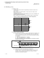
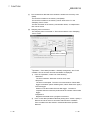
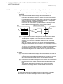
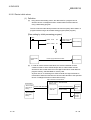
1 OVERVIEW
MELSEC-Q
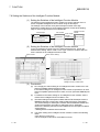
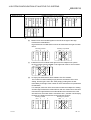
(d)
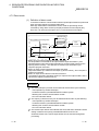
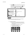
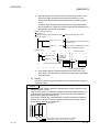
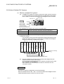
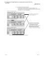
The buffer memory of intelligent function module (e.g. Q64AD, Q62DA) can
be used in the same way as devices when programming.
[For the case of AnS]
[For the case of QCPU]
X0
X0
+P
D0
U4\G12
FROMP
H4
Power supply module
QCPU
Input (16 points)
Input (16 points)
Input (16 points)
Q64AD (16 points)
Q64AD (16 points)
Q62AD (16 points)
Output (16 points)
Output (16 points)
Readout of Q64AD
buffer memory's
address 12 data
K12
D10
K1
+P
D10
D0
:U4\G12
Buffer memory address
designation
Intelligent function
module designation
Input/output Nos.:X/Y40 to X/Y4f
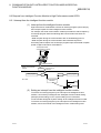
(e)
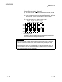
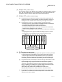
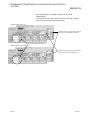
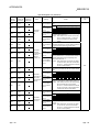
Direct access to link devices (LX, LY, LB, LW, LSB, LSW) of
MELSECNET/10H network modules (e.g. QJ71LP21) is possible without
refresh settings.
X0
+P
J5\W12
D0
Power supply module
QCPU
QJ71LP21
Input (16 points)
Input (16 points)
Q68AD (16 points)
Q68AD (16 points)
Q62AD (16 points)
Output (16 points)
Output (16 points)
Direct readout of the No.5 network module's
"LW12" link register
:J5\W12
Link register designation
Network No. designation
Network No.5
1-9
1-9
1 OVERVIEW
MELSEC-Q
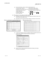
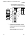
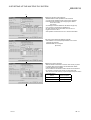
(2) Edge relays simplify pulse conversion processing
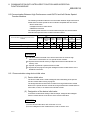
(a)
The use of a relay (V) that comes ON at the leading edge of the input
condition simplifies pulse processing when a contact index qualification has
been made.
[Circuit example]
M1000
RST
Z1
FOR
K1000
Reset index register (Z1)
Repetition (1000 times) designation
X0Z1 V0Z1
M0Z1
Pulsing M0 to M999
M1000
INC
Z1
Increment Index Register (Z1) (+1)
Return to FOR instruction
NEXT
[Timing chart]
ON
X0 OFF
ON
When Z1=0
V0 OFF
ON
M0 OFF
1 Scan
ON
X1 OFF
ON
When Z1=1
V1 OFF
ON
M1 OFF
1 Scan
(3) Simpler data processing
(a)
Real numbers (floating decimal point data) and character string constants
can be used in the programming as they are.
Real number data Real number data
X0
E+P E1.23
D0
R0
Real number ADD instruction
$+P
D5
"CPU" D10
Character string data LINK instruction
E1.23
+
D0
E3.45
D1
"Q"
D6 NUL
"2"
E4.68
R1
Character
string data
Character
string data
D5 "0"
Real number data
R0
+
"CPU"
Character
string data
D10
"0"
D11
"C"
"2"
D12
"U"
"P"
D13
"Q"
NUL
REMARK
: NUL indicates "00H (character string END)".
1 - 10
1 - 10
1 OVERVIEW
MELSEC-Q
(b)
Data processing instructions such as table processing instructions, etc.,
enable high-speed processing of large amounts of data.
X0
FINSP D0
R0
K2
FIF0 table
Insertion Insertion Insertion position
source designation
Instruction for data insertion at table
D0
15
3
R0
4
R1
10
R1
10
R2
20
R2
15
R3
30
R3
20
R4
30
R4
(4)
Easy shared use of sub-routine programs
(a)
A common pointer can be used to call the same sub-routine program from
all sequence programs being executed.
Program A
Common pointer
Subroutine program
P1000 call
M0
0
FIF0 table
R0
SM400 M0
P1000
CALLP P1000
Always
ON
MOV K4X0
R0
MOV K4X20
R0
M0
Program B
RET
P1000 call
M10
0
CALLP P1000
(b)
The use of sub-routine call instructions with arguments simplifies the
creation of sub-routine programs which are called several times.
Argument designation
P0 call
M0
CALLP
0
P0
W0
K4X0
R0
Subroutine program
designation
Argument from FD2
Argument to FD1
Argument to FD0
Argument designation
Always
ON
M0
MOV FD1
FD2
RET
P0 call
M10
CALLP
100
Sub-routine program
Destination data
source data
SM400 M0
P0
MOV FD0 FD2
P0
W10 K4X10 R10
Argument from FD2
Argument to FD1
Argument to FD0
REMARK
For details regarding the argument input/output condition, refer to Section 10.3.1.
1 - 11
1 - 11
2 SYSTEM CONFIGURATION FOR SINGLE CPU SYSTEM
MELSEC-Q
2. SYSTEM CONFIGURATION FOR SINGLE CPU SYSTEM
This section describes the system configuration of the High Performance model
QCPU, cautions on use of the system, and configured equipment.
2.1 System Configuration
The outline of the equipment configuration, configuration with peripheral devices, and
system configuration in the High Performance model QCPU system is described
below.
(1) Equipment configuration in High Performance model QCPU system
MITSUBISHI
MITSUBISHI
LITHIUM BATTERY
Memory card 1
(Q2MEM-1MBS,Q2MEM-2MBF,
Q2MEM-4MBF,Q2MEM-8MBA,
Q2MEM-16MBA,Q2MEM-32MBA)
Extension of the AnS Series module
High Performance model QCPU
(Q02CPU,Q02HCPU,Q06HCPU,
Q12HCPU,Q25HCPU)
Battery
(Q6BAT)
Main base unit
(Q35B,Q38B,Q312B)
Power supply module /
I/O module / Intelligent function
module of the Q Series
2
QA1S6 extension base unit
(QA1S65B,QA1S68B)
Power supply module /
I/O module / Intelligent function
module of the AnS Series
Extension of the Q Series module
Extension cable
(QC06B,QC12B,QC30B,
QC50B,QC100B)
Q6 B extension base unit
(Q65B,Q68B,Q612B)
Power supply module 3 /
I/O module / Intelligent function
module of the Q Series
POINTS
1: The number of memory cards to be installed is one sheet.
The memory card must be selected from SRAM, Flash, and ATA according to
the application and capacity.
With commercial memory cards, the Operation is not assured.
2: QA1S65B and QA1S68B extension base units are used for the power module,
I/O module, and special function module of the AnS series.
3: The Q series power supply is not required for the Q5 B type extension base
unit.
2-1
2-1
2
2 SYSTEM CONFIGURATION FOR SINGLE CPU SYSTEM
MELSEC-Q
(2) Configuration of peripheral devices for High Performance QCPU
2
Memory card 1
(Q2MEM-1MBS,Q2MEM-2MBF,
Q2MEM-4MBF,Q2MEM-8MBA)
High Performance model QCPU
(Q02CPU,Q02HCPU,Q06HCPU,
Q12HCPU,Q25HCPU)
USB cable 1
(To be procured yourself)
Only Q02HCPU, Q06HCPU
Q12HCPU and Q25HCPU
can be used.
RS-232 cable
(QC30R2)
PC card adapter
(Q2MEM-ADP)
Personal Computer
GX Developer or later
(SW4D5C-GPPW-E)
1: For writing into memory card on GX Developer, and USB cable, refer to the
operating manual of the GX Developer.
2-2
2-2
2 SYSTEM CONFIGURATION FOR SINGLE CPU SYSTEM
MELSEC-Q
(3) Outline of system configuration
Main base unit(Q312B)
Power supply module
0 1 2 3 4 5 6 7 8 9 10 11
Extension
cable
1st extension
stage
O
U
T
C
P
U
Slot No.
00 20 40 60 80 A0 C0 E0 100 120 140 160
1F 3F 5F 7F 9F BF DF FF 11F 13F 15F 17F
Extension base unit(Q612B)
Power supply module
12 13 14 15 16 17 18 19 20 21 22 23
180 1A0 1C0 1E0 200 220 240 260 280 2A0 2C0 2E0
O
IU
NT
The figure shows the configuration
when 32-input/output modules are
loaded to each slot.
19F 1BF 1DF 1FF 21F 23F 25F 27F 29F 2BF 2DF 2FF
Extension base unit(Q68B)
Power supply module
24 25 26 27 28 29 30 31
5th extension
stage
Extension base unit(QA1S68B)
Power supply module
45 46 47 48 49 50 51 52
300 320 340 360 380 3A0 3C0 3E0
5A0 5C0 5E0 600 620 640 660 680
O
IU
NT
System configuration
O
IU
NT
31F 33F 35F 37F 39F 3BF 3DF 3FF
5BF 5DF 5FF 61F 63F 65F 67F 69F
Extension base unit(Q68B)
Power supply module
32 33 34 35 36 37 38 39
3rd extension
stage
Extension base unit(QA1S68B)
Power supply module
53 54 55 56 57 58 59 60
6th extension
stage
400 420 440 460 480 4A0 4C0 4E0
6A0 6C0 6E0 700 720 740 760 780
O
IU
NT
O
IU
NT
41F 43F 45F 47F 49F 4BF 4DF 4FF
6BF 6DF 6FF 71F 73F 75F 77F 79F
Extension base unit(Q65B)
Power supply module
40 41 42 43 44
4th extension
stage
Extension base unit(QA1S65B)
Power supply module
61 62 63
7th extension
stage
500 520 540 560 580
7A0 7C0 7E0
O
IU
NT
O
IU
NT
51F 53F 55F 57F 59F
7BF 7DF 7FF
Prohibit
Prohibit
2nd extension
stage
When module is installed,
an error occurs.
Maximum number of
Extension Stages
Maximum number of
I/O modules to be
installed
Maximum number of
I/O points
Main base unit
Extension base unit
Extension cable
Notes
2-3
Seven Extension Stages
64 modules
4096
Q33B, Q35B, Q38B, Q312B
Q52B, Q55B, Q63B, Q65B, Q68B, Q612B, QA1S65B, QA1S68B
QC05B, QC06B, QC12B, QC30B, QC50B, QC100B
(1) Extension bases unit of up to seven stages can be used.
(2) Do not use extension cable longer than an overall extension length of 13.2m(43.31ft.).
(3) When using an extension cable, do not bind it together with the main circuit (high voltage and
heavy current) line or do not lay down them closely to each other.
(4) When setting the No. of the expansion stages, set it in the ascending order so that the same
No. is not set simultaneously by two extension base units.
(5) When Q5 B, Q6 B and QA1S6 B types of extension base units are mixed, first connect the
Q5 B, Q6 B type and then connect the QA1S6 B type.
When setting the No. of the extension stages, set it from Q5 B/Q6 B in order.
Although there are no particular restrictions in the order of the installation of the Q5 B and
Q6 B, refer to Section 6.6 for usability.
(6) Connect the extension cable from OUT of the extension cable connector of the base unit to IN
of the extension base unit on the next stage.
(7) If 65 or more modules are installed, an error will occur.
2-3
2 SYSTEM CONFIGURATION FOR SINGLE CPU SYSTEM
MELSEC-Q
2.2 Precaution on System Configuration
This section describes hardware and software packages compatible with QCPU.
(1) Hardware
(a) The number of modules to be installed and functions are limited depending on
the type of the modules.
Applicable Module
Limit of number of modules
to be installed
Type
• QJ71PL21
• QJ71BR11
Q Series MELSECNET/10H
• QJ71LP21-25
network module
• QJ71LP21G
• QJ71LP21GE
• QJ71E71
Q series Ethernet interface
• QJ71E71-B2
module
• QJ71E71-100
Q series CC-Link system
• QJ61BT11
master local module
Up to 4 units
Up to 4 units
No limit
No limit
(setting of automatic refresh
function not allowed)
MELSECNET/MINI-S3 data • A1SJ71PT32-S3
link module
• A1SJ71T32-S3
AnS series special-function
module shown on the right
Interrupt module
• A1SD51S
• A1SD21-S1
• A1SJ71J92-S3
(When GET/PUT service is used)
• A1SI61
• QI60
Total of 6 units
One unit only
: A maximum of 4 modules if the network parameters for CC-Link are set and
controlled by the GX Developer. There is no restriction in the number of modules
when the parameters are set by the special-purpose instructions for the CC-Link.
For details on the CC-Link System Master Local Unit that can set parameters with
the special-purpose instructions, refer to the manual for the CC-Link Master Local
module.
(b) When the AnS series special-function modules shown below are used, a
limitation is given to an accessible device range.
• A1SJ71J92-S3 type JEMANET interface module
• A1SD51S type intelligent communication
Device
Accessible device range
Input (X), Output (Y)
X/Y0 to 7FF
Internal relay (M), Latch relay (L)
M0 to 8191
Link relay (B)
B0 to FFF
Timer (T)
T0 to 2047
Counter (C)
C0 to 1023
Data register (D)
D0 to 6143
Link register (W)
W0 to FFF
Annunciator (F)
F0 to 2047
(c) A graphic operation terminal can be used only for the GOT900 series (Basic
OS matching Q mode and communication driver must be installed).
The GOT800 series, A77GOT, and A64GOT cannot be used.
2-4
2-4
2 SYSTEM CONFIGURATION FOR SINGLE CPU SYSTEM
MELSEC-Q
(d) The modules shown below cannot be used.
Module Name
Type
MELSECNET/IO network
A1SJ71LP21, A1SJ71BR11, A1SJ71QLP21,
module
A1SJ71QLP21S, A1SJ71QLP21GE, A1SJ71QBR11
MELSECNET (II), /B data link
module
Ethernet interface module
Serial communication module,
computer link module
A1SJ71AP21, A1SJ71AR21, A1SJ71AT21B
A1SJ71QE71-B2-S3(-B5-S3),
A1SJ71E71-B2-S3(-B5-S3)
A1SJ71QC24(N), A1SJ71UC24-R2(-R4/-PRF)
CC-Link master-local module
A1SJ61QBT11, A1SJ61BT11
Modem interface module
A1SJ71CMO-S3
ME-NET interface module
A1SJ71ME81
(e) A dedicated instruction for the next module which was present in the QnA/A
series program instruction cannot be used for the High Performance model
QCPU. Re-writing using FROM/TO instruction is required.
Module Name
Type
High-speed counter module
A1SD61, A1SD62, A1SD62D(-S1), A1SD62E
MELSECNET/MINI-S3
A1SJ71PT32-S3, A1SJ71T32-S3
Positioning module
ID module
A1SD75P1-S3(P2-S3/P3-S3),
A1SD75M1(M2/M3)
A1SJ71ID1-R4, A1SJ71ID2-R4
(2) Software package
(a) Programs for the High Performance Model QCPU can be created using GX
Developer Version 4 or later.
(b) GX Developer Version 6 or later is required to use the functions that have
been added in the High Performance Model QCPU products whose first 5
digits of the serial number are "02092."
(c) GX Developer Version 6 or later is required to use the functions that have
been added in the High Performance Model QCPU products whose first 5
digits of the serial number are "03051."
2-5
2-5
2 SYSTEM CONFIGURATION FOR SINGLE CPU SYSTEM
MELSEC-Q
2.3 Confirming the Serial No. and Function Versions
The QCPU serial No. and function versions can be confirmed on the rating nameplate
and GX Developer's system monitor.
(1) Confirming the serial No. and function versions on the rating
nameplate
MODEL
Serial No. (First five digits)
Function version
SERIAL 03051 0000000000-A
LISTED 80M1
IND.CONT.EQ.
MADE IN JAPAN
(2) Confirming the serial No. and function versions on the system
monitor (list of product information)
The High Performance model QCPU serial No. and function version can be
confirmed with the list of product information on the GX Developer (Version 6 or
later) system monitor.
The intelligent function module High Performance model QCPU's serial No. and
function version can also be confirmed.
Serial number
2-6
Function version
2-6
3 PERFORMANCE SPECIFICATION
MELSEC-Q
3 PERFORMANCE SPECIFICATION
Performance specification of QCPU module is as follows:
Table 3.1 Performance specification
Model name
Item
Q02CPU
Q02HCPU
Control method
Processing speed
(sequence instructions)
Relay symbol language, logic symbolic language,
MELSAP-3 (SFC)
0.079µs
0.034µs
MOV D0 D1
0.237µs
0.102µs
360 (except intelligent function module dedicated instruction)
Constant scan
(function to make regular scan time)
Program memory (drive
0)
Set parameter values to
specify
0.5 to 2000 ms (configurable in multiple of 0.5 ms)
28k steps
60k steps
124k steps
252k steps
See Section 6.2
Memory card (RAM)
(drive 1)
Capacity of loading memory cards (1 Mbyte maximum)
See Section 6.5
Memory card (ROM)
(drive 2)
Capacity of loading memory cards
(Flash card: 4 Mbyte maximum, ATA card 32 Mbyte maximum)
See Section 6.5
Standard RAM (drive 3)
Standard ROM (drive 4)
112 kbyte
496 kbyte
See Section 6.4
1008 kbyte
See Section 6.3
60
See Section 14.2.4
124
252
See Section 6.2
256
See Section 6.5
Flash
card
288
See Section 6.5
ATA card
512
See Section 6.5
2
1 file each for file
register and local
device, see Section 6.4
Standard RAM
Standard ROM
240 kbyte
8 kbyte
28
Memory card (RAM)
Memory card
(ROM)
3
256 kbyte
64k byte
PLC share memory
Program memory
Maximum
number of
stored files
Remark
Direct input/output is
possible by direct
input/output specification
(DX , DY )
LD X0
Number of instructions
Memory
capacity
Q25HCPU
Refresh mode
Program language
(Sequence control dedicated language)
2
Q12HCPU
Repetitive operation of stored program
I/O control method
Program
capacity
Q06HCPU
28
60
124
252
1
See Section 6.3
I/O device points
8192 points (X/Y0 to 1FFF)
Number of usable points
in program
I/O points
4096 points (X/Y0 to FFF)
Number of points
accessible to actual
input/output modules
1: Maximum number of executable program is 124. More than 124 programs can not be executed.
2: The maximum number of sequence steps (in the case of a single program) that can store the parameters in other drive and can be
executed by CPU module is obtained from the following equation: (Program capacity) - (File header size (default: 34 steps))
For details on the program capacity and files, see Chapter 6.
3: The memory capacity of the Q12HCPU and Q25HCPU with the first five digits of the serial number being "02091" or earlier is 64 kbyte.
4: The shared CPU memory will not be latched.
The shared CPU memory will be cleared when the PLC's power is switched on or the CPU module is reset.
3-1
3-1
3
3 PERFORMANCE SPECIFICATION
MELSEC-Q
Table 3.1 Performance specification (continued)
Model name
Item
Q02CPU
Internal relay [M]
Q06HCPU
Q12HCPU
Q25HCPU
Latch relay [L]
Default 8192 points (L0 to 8191)
Link relay [B]
Default 8192 points (B0 to 1FFF)
Default 2048 points (T0 to 2047) (for low/high speed timer)
Select between low/high speed timer by instruction
Set the measurement module of low/high speed timer by parameter
(Low speed timer: 1 to 1000 ms, 1 ms/unit, default 100 ms)
(High speed timer: 0.1 to 100ms, 0.1 ms/unit, default 10 ms)
Timer [ T ]
Retentive timer [ST]
Default 0 point (for low/high speed timer)
Select between low/high speed retentive timer by instruction
Set the measurement module of low/high speed retentive timer by
parameter
(Low speed retentive timer: 1 to 1000 ms, 1 ms/unit, default 100 ms)
(High speed retentive timer: 0.1 to 100ms, 0.1 ms/unit, default 10 ms)
Counter [C]
• Normal counter default 1024 points (C0 to 1023)
• Interrupt counter maximum 256 points (default 0 point, set via parameter)
Data register [D]
Default 12288 points (D0 to 12287)
Link register [W]
Default 8192 points (W0 to 1FFF)
Annunciator [F]
Default 2048 points (F0 to 2047)
Edge relay [V]
Set parameter
values to specify
usable point
Default 2048 points (V0 to 2047)
[R]
File register
[ZR]
3-2
Remark
Default 8192 points (M0 to 8191)
3
Number of device points
Q02HCPU
• When standard RAM is used: 32768 points (R0 to 32768)
• When standard SRAM card is used:
may use up to maximum of 517120 points by block conversion by
32768 points (R0 to 32767) unit
• When flash card (2 Mbyte) is used:
may use up to maximum of 1040384 points by block conversion by
32768 points (R0 to 32767) unit
• When flash card (4 Mbyte) is used:
may use up to maximum of 1042432 points by block conversion by
32768 points (R0 to 32767) unit
When flash card is
used, only read
process is enabled
• When standard RAM is used: 32768 points (ZR0 to 32767)
• When standard SRAM card is used:
517120 points (ZR0 to 517119), no block conversion necessary
• When flash card (2 Mbyte) is used:
1040384 points (ZR0 to 1040383), no block conversion necessary
• When flash card (4 Mbyte) is used:
1042432 points (ZR0 to 1042431), no block conversion necessary
3-2
3 PERFORMANCE SPECIFICATION
MELSEC-Q
Table 3.1 Performance specification (continued)
Model name
Item
Q02CPU
Q02HCPU
Q12HCPU
Special link relay [SB]
2048 points (SB0 to 7FF)
Special link register [SW]
2048 points (SW0 to 7FF)
Step relay [S]
8192 points (S0 to 8191)
Index register [Z]
Number of device points
Q06HCPU
Q25HCPU
Remark
16 points (Z0 to 15)
4096 points (P0 to 4095), set parameter values to select usable range of
in-file pointer/shared pointers
Pointer [P]
256 points (IO to 255)
set parameter values to select periodic interval of system interrupt
pointers I28 to I31 (0.5 to 1000 ms, 0.5 ms/unit)
default I28: 100ms I29: 40ms I30: 20ms I31: 10ms
Interrupt pointer [ I ]
Special relay [SM]
2048 points (SM0 to 2047)
Special register [SD]
2048 points (SD0 to 2047)
Function input [FX]
16 points (FX0 to F)
Function output [FY]
16 points (FY0 to F)
Function register [FD]
Number of device
points is fixed.
5 points (FD0 to 4)
Link direct device
Device for direct access of link devices.
For MELSECNET/H use only.
Specified form :J
,J
, J
\X
\Y
J
\B
\SW
,J
,J
Intelligent function module device
Device for direct access of intelligent function module buffer memory.
Specified form : U
\G
,
Latch (power failure compensation) range
L0 to 8191 (default)
(Latch range may be specified for B, F, V, T, ST, C, D, W)
Remote RUN/PAUSE contact points
May specify one RUN/PAUSE contact point each by X0 to 1FFF.
Clock function
Year, month, date, hour, minute, second, day of week
(auto-detects leap years)
Accuracy : -3.18 to +5.25s (TYP. +2.12s)/d at 0 C
Accuracy : -3.93 to +5.25s (TYP. +1.90s)/d at 25 C
Accuracy : -14.69 to +3.53s (TYP. -3.67s)/d at 55 C
Allowable momentary power failure period
\W
\SB
,
Set parameter
values to specify
By power supply module
5.V.DC internal current consumption
0.60A
Mass
0.20kg
External dimension [mm (in)}
0.64A
0.64A
0.64A
0.64A
0.20kg
0.20kg
0.20kg
0.20kg
98 (H) × 27.4 (W) × 89.3 (D) (3.86 × 1.08 × 3.52)
REMARK
Refer to the High Performance model QCPU (Q Mode) User's Manual (Hardware
Design, Maintenance and Inspection), for details for QCPU general specification.
3-3
3-3
4 SEQUENCE PROGRAM CONFIGURATION & EXECUTION
CONDITIONS
MELSEC-Q
4 SEQUENCE PROGRAM CONFIGURATION & EXECUTION CONDITIONS
Sequence programs and SFC programs can be executed at the High Performance
model QCPU.
This chapter describes the sequence program configuration and execution conditions.
SFC programs are not described in this manual.
For details regarding SFC programs, refer to the QCPU (Q mode)/QnACPU
Programming Manual (SFC).
4.1 Sequence Program
(1) Definition of sequence program
(a)
A sequence program is created using sequence instructions, basic
instructions, and application instructions, etc.
Sequence instruction
X0
M0
K100
T0
4
T0
Y30
Basic instruction
X1
BIN
K4X10
D0
Application instruction
X41
FROM
(b)
H5
K0
D10
K1
There are 3 types of sequence program: main routine programs, sub-routine
programs, and interrupt programs.
For details regarding these programs, refer to the following sections of this
manual:
• Main routine programs
: Section 4.1.1
• Sub-routine programs
: Section 4.1.2
• Interrupt programs
: Section 4.1.3
File A
Main routine
program
FEND
P0
Sub-routine
program
RET
I0
Interrupt
program
IRET
END
REMARK
For details regarding the sequence instructions, basic instructions, and application
instructions, refer to the " QCPU (Q Mode)/QnACPU Programming Manual
(Common Instructions)".
4-1
4-1
4 SEQUENCE PROGRAM CONFIGURATION & EXECUTION
CONDITIONS
MELSEC-Q
(2) Sequence program writing format
Programming for sequence programs is possible using either ladder mode, or list
mode.
(a)
Ladder mode
• The ladder mode is based on the relay control sequence ladder.
Programming expressions are similar to the relay control sequence ladder.
• Relay symbolic language programming occurs in ladder block units.
A ladder block is the smallest unit of sequence program processing, with
the ladder beginning from the left bus and ending at the right bus.
Left bus
0
Step No.
a Contact
b Contact
Coil (output)
Right bus
X0
X1
Y20
X2
X3
Y21
2
Ladder blocks
Y22
4
Y23
8
X4
X5
Y24
Y24
X0 to X5
: Indicate inputs.
Y20 to Y24 : Indicate outputs.
Fig.4.1 Ladder Block
(b)
List mode
The list mode uses dedicated instructions instead of the contact symbols,
coil symbols, etc., used in the ladder mode.
Contact a, contact b and coil instructions are as follows:
• a contact ............LD, AND, OR
• b contact ............LDI, ANI, ORI
• coil......................OUT
(2) Program processing
Sequence programs are processed in order, beginning from step 0 and ending at
the END/FEND instruction.
Processing of ladder mode ladder blocks begins from the left bus, and proceeds
from left to right. When one ladder block is completed, processing proceeds
downward to the next ladder block.
[List mode]
[Ladder mode]
Left to right
1) 2) 7) 8) 9)
X0 X1 X5 X6 X7
0
3) 4)
X2 X3
Top to
bottom
10)
Y10
5)
6)
X4
10
11)
END
Numbers 1) to 11) indicate the processing
order of the sequence program.
0 LD
1 AND
2 LD
3 AND
Executed in
4 ORB
order, beginning 5 OR
from step 0 to
6 AND
7 AND
the ending at
8 AND
the END
9 OUT
instruction.
10 END
X0
X1
X2
X3
X4
X5
X6
X7
Y10
1)
2)
3)
4)
5)
6)
7)
8)
9)
10)
11)
Step No.
Fig.4.2 Sequence Program Processing
4-2
4-2
4 SEQUENCE PROGRAM CONFIGURATION & EXECUTION
CONDITIONS
MELSEC-Q
4.1.1 Main routine program
(1) Definition of main routine program
(a)
(b)
A main routine program is a program which begins from step 0 and ends at
the END/FEND instruction. 1
The main routine program execution begins from step 0 and ends at the
END/FEND instruction.
1) If only one program is being executed, processing will begin from step
0 again after the END/FEND instruction is processed.
Step 0
Program execution
Main routine
program
Returns to step 0 when only one
program is being executed.
END/FEND
END/FEND
END processing
2)
If multiple programs are being executed, processing which occurs after
the END/FEND instruction varies according to the designated
execution conditions.
(2) Execution conditions for main routine programs
2
If multiple programs are being executed, the following five types of execution
conditions can be designated by the program in the PLC parameters according to
the application in question.
• Initial execution program
: See Section 4.2.1.
• Scan execution type program
: See Section 4.2.2.
• Low-speed execution program
: See Section 4.2.3.
• Stand-by type program
: See Section 4.2.4.
• Fixed scan execution type program : See Section 4.2.5.
REMARK
1: For details regarding the END/FEND instruction, refer to the "QCPU (Q
mode)/QnACPU Programming Manual (Common Instructions)".
2: If only one program is executed, it is processed under the "scan execution type
program" condition without designation by the program in the PLC parameters.
4-3
4-3
4 SEQUENCE PROGRAM CONFIGURATION & EXECUTION
CONDITIONS
MELSEC-Q
4.1.2 Sub-routine programs
(1) Definition of sub-routine program
(a)
(b)
(c)
A sub-routine program is a program which begins from a pointer (P ) and
ends at a RET instruction.
A sub-routine program is executed only when called by a CALL instruction
(e.g. CALL(P), FCALL(P)) from the main routine program.
Sub-routine program application
1) The overall step count can be reduced by using a sub-routine program
as a program which is executed several times in one scan.
2) The step count of a constantly executed program can be reduced by
using a sub-routine program as a program which is executed only
when a given condition is satisfied.
(2) Sub-routine program management
Sub-routine programs are created after the main routine program (after FEND
instruction), and the combination of main and sub-routine programs can be
managed as one program.
(a)
When created after the main routine program
• A sub-routine program is created between the main routine program's
FEND and END instructions.
• Because there are no restrictions regarding the order in which sub-routine
programs are created, there is no need to set the pointers in ascending
order when creating multiple sub-routine programs.
• Either a local pointer or a common pointer may be used.
High Performance model QCPU
Program A
Program memory / Standard
ROM / Memory card
Main routine
program
Write
Program A
FEND
P0
Y10
RET
Sub-routine
program
P8
Y11
RET
P1
Y12
RET
END
REMARK
: See Section 10.9 for details regarding local and common pointers.
See Section 10.8 for details regarding sub-routine program nesting.
4-4
4-4
4 SEQUENCE PROGRAM CONFIGURATION & EXECUTION
CONDITIONS
MELSEC-Q
(b)
4-5
Using the sub-routine program as a separate program
Sub-routine programs can also be managed as separate, discrete
programs (stand-by type programs). (See Section 4.2.4 for details
regarding stand-by type programs).
4-5
4 SEQUENCE PROGRAM CONFIGURATION & EXECUTION
CONDITIONS
MELSEC-Q
4.1.3 Interrupt programs
(1) Definition of interrupt program
(a)
(b)
An interrupt program is a program which begins at the interrupt pointer
(I ), and ends at the IRET instruction. 1
Interrupt programs are executed only when an interrupt factor occurs. 1
(2) Interrupt program management
Interrupt programs are created after the main routine program (after the FEND
instruction), and the combination of main and sub-routine programs can be
managed as one program.
(a) When created after the main routine program
• An interrupt program is created between the main routine program's
FEND and END instructions.
• Because there are no restrictions regarding the order in which interrupt
programs are created, there is no need to set the interrupt pointers in
ascending order when creating multiple interrupt programs.
High Performance model QCPU
Program A
Program memory/ Standard
ROM / Memory card
Main routine
program
Write
Program A
FEND
I0
Y10
IRET
Interrupt
program
I32
Y11
IRET
I28
Y12
IRET
END
Interrupt pointer
(b)
Using the interrupt program as a separate program
Interrupt programs can also be managed as separate, discrete programs
(stand-by type programs). (See Section 4.2.4 for details regarding stand-by
type programs).
However, the same interrupt program pointer number cannot be used more
than once in the program being executed by the QCPU.
REMARK
1: See Section 10.10 for details regarding interrupt factors and interrupt pointers.
4-6
4-6
4 SEQUENCE PROGRAM CONFIGURATION & EXECUTION
CONDITIONS
MELSEC-Q
(3) Executing interrupt programs
(a)
In order to execute an interrupt program with the interrupt pointer I32
through I47, IMASK and EI instructions are required to obtain permission
for the interruption. 1
1) If an interrupt factor occurs prior to an interruption permitted status, the
interrupt program for the factor in question will be executed when an
interruption permitted status is established.
2)
If an interrupt factor occurs during a STOP/PAUSE, the interrupt
program for the factor in question will be executed when an
"interruption permitted" condition is established following a return to the
RUN status.
Interrupt program example
Interrupt program execution
Program execution
Interrupt program for
"I0" activated
EI
Main routine
program
FEND
End of main
routine program
I0
Interrupt program
for "I29" activated
FEND
Interrupt
program
I0
IRET
"I0" interrupt
program
I29
Interrupt
program
I29
IRET
"I29" interrupt
program
END
END
Fig.4.3 Interrupt Program Execution
(b)
When an interrupt factor occurs, the interrupt program with the interrupt
pointer number corresponding to that factor is executed.
However, interrupt program execution varies according to the condition at
that time.
1) If two or more interrupts occur at the same time:
The interrupt programs are executed, starting with the one
corresponding to an interrupt pointer number (I
) of the highest
priority. 2
The remaining interrupt programs remain on stand-by until processing
of the higher priority interrupt program is completed.
If the same interrupt factor as that being executed occurs before the
interrupt program is processed, the interrupt factor is stored in the
memory and, after the interrupt program has been processed, the
same interrupt program is executed again.
2)
4-7
When an instruction is being executed:
Interruptions are prohibited during execution of instructions.
If an interrupt factor occurs during execution of an instruction, the
interrupt program will be executed after processing of the instruction is
completed.
4-7
4 SEQUENCE PROGRAM CONFIGURATION & EXECUTION
CONDITIONS
MELSEC-Q
3)
Interruption during a network refresh:
If an interrupt factor occurs during a network refresh operation, the
network refresh operation is suspended, and the interrupt program is
executed.
This means that "assurance of blocks in cyclic data at each station"
cannot be secured by using a device designated as a destination of
link refresh operation on the MELSECNET/H Network System. 3
10ms
10ms
10ms
10ms
Interrupt factor
Interrupt program
execution
Network refresh
execution
Network refresh operation is suspended,
and the interrupt program is executed.
Fig.4.4 Interruption during Network Refresh Operation
4)
(c)
Interruption during END processing:
If an interrupt factor occurs during an END processing waiting period
during constant scanning, the interrupt program corresponding to that
factor will be executed.
See Section 10.6.2 for details regarding index register processing when
switching to an interrupt program from a scan execution type program or
low-speed execution program.
(4) High-speed execution of an interrupt program and overhead time
By default, High Performance model QCPU will perform the following process when
executing an interrupt program:
• To hide and restore an index register. (See section 10.6.2)
• To hide and restore the file name of a file register in use.
The above-listed processes are not performed if an option to "Execute at a High
Speed" is selected in the PLC System Setting sheet of the PLC Parameter dialog box.
This will make it possible to shorten the duration of overhead time required for
execution of an interrupt program.
CPU TYPE
Q02CPU
Q02HCPU, Q06HCPU,
Q12HCPU, Q25HCPU
OVERHEAD TIME ( s)
LOW-SPEED EXECUTION
HIGH-SPEED EXECUTION
380
230
165
100
REMARK
1: For details regarding the IMASK and EI instructions, refer to the "QCPU (Q
mode)/QnACPU Programming Manual (Common Instructions).
To execute interrupt programs I0 through I31 and I48 through I255, use an EI
instruction to enter the interrupt programs into an interrupt enabled status.
2: See Section 10.10 for details regarding the priority ranking of interrupt programs.
3: For assurance of station unit blocks in cyclic data, see the "MELECNET/H
Network System Reference Manual."
4-8
4-8
4 SEQUENCE PROGRAM CONFIGURATION & EXECUTION
CONDITIONS
MELSEC-Q
(5) Program creation restrictions
(a)
A device which is switched ON by a PLS instruction in an interrupt program
will remain ON until that interrupt program is executed again.
X0
END
0
X0
PLS M0
IO IRET END 0
END
0 IO
IRET END
PLS M0
0
ON
X0 OFF
ON
M0 OFF
Switched OFF by PLS M0 instruction
Switched ON by PLS M0 instruction at X0 leading edge (OFF to ON)
(b)
A DI status (interruption prohibited) is established during execution of an
interrupt program.
Do not execute EI/DI instructions in the interrupt program.
(c)
Timers cannot be used in interrupt programs.
As timers are used at OUT T
instructions to update present values and
switch contacts ON and OFF, the use of a timer in the interrupt program
would make a normal time count impossible.
(d)
The following commands cannot be used in the interrupt program.
• COM
• ZCOM
• EI
• DI
(e)
When the interrupt program/fixed scan execution type program is executed
when measuring time such as the scan time or execution time, the
measured time will become the value obtained by adding the interrupt
program/fixed scan execution type program.
Thus, if the interrupt program/ fixed scan execution type program is
executed, the values stored in the following special registers and
GX Developer monitor values will become longer than when the interrupt
program/ fixed scan execution type program is not executed.
1) Special registers
• SD520, SD521: Current scan time
• SD522, SD523: Initial scan time
• SD524, SD525: Minimum scan time
• SD526, SD527: Maximum scan time
• SD528, SD529: Current scan time for low speed
• SD532, SD533: Minimum scan time for low speed
• SD534, SD535: Maximum scan time for low speed
• SD540, SD541: END processing time
• SD542, SD543: Constant scan wait time
• SD544, SD545: Cumulative execution time for low speed execution
type programs
• SD546, SD547: Execution time for low speed execution type
programs
• SD548, SD549: Scan program execution time
• SD551, SD552: Service interval time
2)
4-9
GX Developer monitor values
• Execution time measurement
• Scan time measurement
• Constant scan
4-9
4 SEQUENCE PROGRAM CONFIGURATION & EXECUTION
CONDITIONS
MELSEC-Q
4.2 Program Execute Type
Programs executed by the High Performance model QCPU can be stored in the High
Performance model QCPU's program memory, standard ROM or memory card.
Programs can be stored in the standard ROM or memory card as a single program, but
also as multiple programs by splitting them into separate programs for each control
function.
This permits the programming procedure to be split up among several program
designers, who can design separate programs for each operation and can store them
in the standard ROM or memory card.
When multiple programs are executed by the High Performance model QCPU,
"program name (file name)" and "execute type" settings of the programs must be
designated.
Control by one program
Control by separating
into multiple programs
Program A
Control contents A
Control contents A
Program B
Control contents B
Control contents B
Store by separating
the code according
to control contents.
Program n
Control contents n
4 - 10
Control contents n
4 - 10
4 SEQUENCE PROGRAM CONFIGURATION & EXECUTION
CONDITIONS
MELSEC-Q
(1) Execute Type Setting
(a)
To execute several programs, specify a "Program name" and "Execute
type" of each program in the Program Setting sheet of the PLC Parameter
dialog box.
High Performance model QCPU will execute selected programs in the
order of specified Execute Type setting.
1)
2)
3)
4)
5)
6)
4 - 11
1)
Program name
This column is used to specify a program name (file name) of the
program to be executed by High Performance model QCPU.
2)
Execute type
This column is used to specify the execute type of the program defined
in the "Program name" column. See Section (b).
3)
Fixed scan
This column is used to specify time intervals at which to an execution
type program.
The Fixed Scan setting range is determined by the units of time
intervals as follows:
• In the unit "ms": 0.5 to 999.5
• In the unit "s": 1 to 60
4)
In units
This column is used to specify the units (ms/s) of fixed scan intervals.
4 - 11
4 SEQUENCE PROGRAM CONFIGURATION & EXECUTION
CONDITIONS
MELSEC-Q
5)
File Use Setting
The PLC File Setting sheet of the PLC Setting dialog box has several
options: file register, device's initial value, comment, and local device.
Specify whether to use files of these options for each program. By
default, the option "Use PLC file setting" is selected. If the option "Not
used" is selected, the File Use setting is made as listed below in the table.
Setting item
File register
File registers can not be used in the program.
Device initial value
Comment
6)
(c)
4 - 12
The device initial value is not set when the program file name and
the device initial value is the same.
Comments can not be used in the program.
Local device
(b)
Processing when the option "Not used" is selected
Local devices are not hidden or restored at the time of program
conversion.
I/O Refresh Setting
High Performance model QCPU uses the I/O Refresh setting to
update output and input from an I/O module and an intelligent-function
module.
The I/O Refresh Setting button is used to update the range of selected
programs. Make the I/O Refresh setting for a scan execution type
program if you want to receive an input (X) or produce an output (Y)
before executing the fixed scan execution type program.
There are following 5 execute types:
1)
Initial execution (Initial)
This program type is executed once only at power ON or when STOPRUN switching occurs. (See Section 4.2.1)
2)
Scan execution (Scan)
This program type is executed once per scan, beginning from the scan
which follows execution of the initial execution program. (See Section 4.2.2)
3)
Low-speed execution (Low speed)
This program type is executed only when a constant scan setting is
made or when a time is set for execution of low-speed execution
programs.
• When a constant scan setting is made, the program is executed
during the surplus time of a scan execution type program.
• When a time for execution of low-speed execution programs is set,
the program is executed during this set time. (See Section 4.2.3.)
4)
Stand-by (Wait)
This program is executed only when its execution is requested. (See
Section 4.2.4.)
5)
Fixed scan execution (Fixed scan)
Program that is executed at time intervals specified in the "Fixed scan"
and "In units" columns of the Program Setting sheet of the PLC
Parameter dialog box. (See Section 4.2.5.)
Scantimes of programs being executed (except the fixed scan execution
type program) can be checked on the monitor of the program list. (See
Section 7.11.1.)
4 - 12
4 SEQUENCE PROGRAM CONFIGURATION & EXECUTION
CONDITIONS
MELSEC-Q
(2) Flow of each program of High Performance model QCPU
The flow of each program after power-ON or STOP to RUN switching of the High
Performance model QCPU is shown below.
Power ON/STOP to RUN
Executed only once at power ON
or STOP to RUN.
Initial execution
type program
Run only when "constant scan" or
Low-speed execution
type program
"low-speed program execution time"
has been set.
END processing
Fxied scan execution
type program
Scan type
program
Stand-by type
program
Program run at specified cyclic
time intervals
Run only when execution request
is given.
POINT
(1) Not all execute types need to be set for the High Performance model QCPU.
Use the items marked with " " as needed, such as the Initial execution, lowspeed execution, stand-by and fixed scan execution type programs.
4 - 13
4 - 13
4 SEQUENCE PROGRAM CONFIGURATION & EXECUTION
CONDITIONS
MELSEC-Q
(3) Changing the Execute Type
(a)
The Execute Type setting made in the Program Setting sheet of the PLC
Parameter dialog box can be changed at any time while a sequence
program is executed. To change the execute type of a program, use a
PSCAN, PLOW, PSTOP or POFF instruction.
PLOW
PSCAN
Initial execution
type program
PSTOP
POFF
PSCAN
Scan execution
type program
PSTOP
POFF
PSTOP
POFF
PSCAN
Stand-by type
program
(b)
Executed instruction
Execute type before change
Scan execution type
Initial execution type
Fixed scan execution type
PLOW
PLOW
PSTOP
POFF
PSCAN
1
Fixed scan execution
type program
The table below shows the timing of changing the execute type of a
program by using a PSCAN, PLOW, PSTOP or POFF instruction.
PSCAN
No change - remains
scan execution type.
Becomes scan
execution type.
Stand-by type
Low-speed execution type
Low-speed execution
type program
Low-speed execution
type execution is
stopped: becomes
scan executions from
the next scan.
(Execution from step
0.)
Becomes scan
execution type.
PSTOP
Becomes stand-by
type.
POFF
PLOW
Output is turned OFF
in the next scan.
Becomes stand-by
Becomes low-speed
type from the next
type.
scan after that.
No change - remains
No processing.
stand-by type.
Low-speed execution
type execution is
stopped: becomes
scan executions from
the next scan.
Low-speed execution
type execution is
stopped, and output is No change - remains
low-speed
turned OFF in the
next scan. Becomes executions.
stand-by type from the
next scan after that.
Becomes stand-by
type.
Output is turned OFF
in the next scan.
Becomes low-speed
Becomes stand-by
type.
type from the next
scan after that.
POINT
1: If the fixed scan execution type program is changed to another execution type,
you cannot return to the fixed scan execution type.
4 - 14
4 - 14
4 SEQUENCE PROGRAM CONFIGURATION & EXECUTION
CONDITIONS
MELSEC-Q
4.2.1 Initial execution type program
(1) Definition of initial execution type program
(a)
An initial execution type program is executed once only at power ON, or
when STOP to RUN switching occurs.
(b) This program's execute type is designated as "initial" in the program of the
PLC parameters.
(c) In the same manner as the initial processing for the intelligent function
module, the initial execution program is executed only once, and is not
required in subsequent scans.
An instruction that contains a complete device cannot be used for an initial
execution type program because the complete device needs several scans
to complete the execution.
Control with one program
Using initial execution type program
Program A
Initial execution
type program
Initial program
Program B
Program to execute
at every scan
Division into initial
execution type program
and scan execution type
Scan execution
type program
(2) Using multiple initial execution type programs
When multiple initial execution type programs are used, they are executed one
by one in ascending number order of the program in the PLC parameters.
(3) END processing
END processing occurs when all initial execution type programs are completed,
and the "scan execution type program" is then executed from the next scan.
Power supply ON/STOP to RUN
Initial execution
type program A
Initial execution
type program B
1 Scan
Executed by program
setting order.
Initial execution
type program n
END processing
Scan execution
type program
4 - 15
4 - 15
4 SEQUENCE PROGRAM CONFIGURATION & EXECUTION
CONDITIONS
MELSEC-Q
(4) Initial scan time
(a)
This is the execution time period for initial execution type programs.
If multiple initial execution type programs are used, this is the execution
time period in which all those programs are executed.
When an interrupt program/fixed cycle execution type program is executed
while an initial execution type program is running, the execution time of the
interrupt program/fixed cycle execution type program will be added to the
initial execution type program.
(b)
The High Performance model QCPU measures the initial scan time and
stores the result in special registers (SD522, SD523). 1
The initial scan time can therefore be checked by monitoring the SD522
and SD523 special registers.
SD522
SD523
Stores less than 1 ms initial scan time (unit
s)
Stores the initial scan time in 1 ms units.
If the SD522 value is "3", and the SD523 value is "400", the initial scan time is
3.4 ms.
POINT
1: The accuracy of the initial scan time stored at the special registers is ± 0.1 ms.
The initial scan time count will continue even if a watchdog time reset
instruction (WDT) is executed at the sequence program.
(5) Initial execution monitor time
(a)
The execution period of the initial execution type program can be monitored
by this timer. The default value is not set.
When monitoring the execution time of the initial execution type program,
designate the Initial execution monitor time in a 10 ms to 2000 ms range at
the PLC RAS settings in the PLC parameter. (Setting unit: 10 ms)
(b)
The low-speed execution type program is executed after the execution of
the initial execution type program is completed.
To use the low-speed execution type program, specify the time that is
longer than the sum of the initial scan time and the execution time of the
low-speed execution type program.
(c)
When the initial scan time exceeds the set initial execution monitor time,
"WDT ERROR (error code: 5000)" occurs, and CPU module operation is
stopped.
POINT
When the initial execution monitor time is designated, there will be a 10 ms error in
the count value.
Therefore, a monitor time setting (t) of 10 ms will result in a "WDT ERROR" when
the initial scan time is in the range 10 ms < t < 20 ms.
4 - 16
4 - 16
4 SEQUENCE PROGRAM CONFIGURATION & EXECUTION
CONDITIONS
MELSEC-Q
4.2.2 Scan execution type program
(1) Definition of scan execution type program
(a)
(b)
Scan execution type programs are executed once per scan, beginning from
the scan which follows execution of the initial execution type program.
Set the execute type to "scan" in the program of PLC parameters.
(2) Executing multiple scan execution type programs
When multiple scan execution type programs are used, they are executed one by
one in ascending number order of the program in the PLC parameters.
(3) END processing
END processing occurs when all initial execution type programs are completed,
and the scan execution type program is then executed from the next scan.
The END processing (network refresh) can be performed for each program while
several scan execution type programs are executed. To do this, include a COM
instruction at the end of each scan execution type program.
STOP to RUN
Power ON to RUN
First scan
Second scan
Third scan
Forth scan
END processing
Initial execution type program
0
0
END
END
0
END
Scan execution type program A
0
END
0
0
END
Scan execution type program B
0
Scan execution type program C
END
0
END
Scan time
(4) Constant scan setting
1
When constant scanning is designated, the scan execution type program is
executed at each designated constant scan period.
REMARK
1: The "constant scan" function executes the scan type program repeatedly at
regular intervals.
For details regarding of the constant scan, refer to Section 7.2.
4 - 17
4 - 17
4 SEQUENCE PROGRAM CONFIGURATION & EXECUTION
CONDITIONS
MELSEC-Q
(5) Scan time
(a)
(b)
The "scan time" is a total of following the execution time of the scan
execution type program and END processing.
If multiple scan execution type programs are used, the "scan time" is the
total time required to execute all the programs.
When an interrupt program/fixed cycle execution type program is executed,
the value added to the interrupt program/fixed cycle execution type
program's execution time will become the scan time.
The scan time present value, minimum value, and maximum value are
measured at the High Performance model QCPU, and the results are
stored in special registers (SD520, SD521, and SD524 to SD527). 1
The initial scan time can therefore be checked by monitoring the SD520,
SD521, and SD524 to SD527 special registers.
Current value
SD520
SD521
Minimum value
SD524
SD525
Maximum value
SD526
SD527
Stores less than 1 ms initial scan time (unit
s)
Stores the initial scan time in 1 ms units.
If the SD520 value is 3, and the SD521 value is 400, the initial scan time is 3.4
ms.
POINT
1: The accuracy of the scan time stored at the special registers is ± 0.1 ms. The
scan time count will continue even if a watchdog timer reset instruction (WDT)
is executed at the sequence program.
(6) WDT (Watchdog timer)
This is the timer which monitors the scan time, and its default setting is 200 ms.
This WDT setting can be designated in a 10 ms to 2000 ms range in the PLC
RAS settings of the PLC parameter.
(Setting units: 10 ms)
When using the low-speed execution program, set the WDT greater than the
scan time plus the execution time of the low-speed execution program.
If the scan time (execution time for scan execution type program + low-speed
execution program) exceeds the WDT setting value, a "WDT ERROR (error
code: 5000)" occurs, and High Performance model QCPU operation is stopped.
POINT
The WDT measurement error is 10 ms.
Therefore, a WDT setting (t) of 10 ms will result in a "WDT ERROR" if the scan
time is in the following range: 10 ms < t < 20 ms.
REMARK
1) Use the GX Developer's Program Monitor List to check the execution time of a
program being executed. See Section 7.11.1 for further information on the GX
Developer's Program Monitor List.
4 - 18
4 - 18
4 SEQUENCE PROGRAM CONFIGURATION & EXECUTION
CONDITIONS
MELSEC-Q
4.2.3 Low-speed execution type program
(1) Definition of low-speed execution type program
(a)
(b)
(c)
Low-speed execution type programs are executed only during "constant
scanning surplus time" or during the period designated for "low-speed
execution program execution time".
1) For a constant scan time with enhanced control accuracy, designate a
constant scan time setting at the PLC RAS in the PLC parameter.
(Setting range: 0.5 to 2000 ms, setting units: 0.5 ms)
2) To secure execution time for low-speed execution type programs at
each scan, designate a low-speed execution program execution time
in the PLC RAS of the PLC parameter.
(Setting range: 1 to 2000 ms, setting units: 1 ms)
3) In order to execute a low-speed execution type program, set either the
constant scan time or low-speed execution program execution time.
Set the execute type of the low-speed execution program to "low speed" in
the program of the PLC parameters.
The low-speed execution type program is used for programs which do not
require execution in each scan, for example programs for printer output.
(2) Executing multiple low-speed execution type programs
When multiple low-speed execution type programs are used, they are executed
one by one in ascending number order of the program in the PLC parameters.
(3) Execution time of the Low-speed execution type program to be
executed per scan
(a)
If all the low-speed execution type program operation is completed within
one scan and there is surplus time, the processing executed after that
depends on the ON/OFF status of special register SM330 and the
execution condition for low-speed execution type programs.
1) Asynchronous method (SM330 = OFF)
Method in which low-speed execution type program operation is
continued in the surplus time.
2) Synchronous method (SM330 = ON)
Method in which even if there is surplus time, low-speed execution
type program operation is not continued, and operation starts again
from the next scan.
Operation method for low- SM330
speed execution type
setting
programs
status
4 - 19
Execution condition for low-speed execution type programs
When constant scan time When low-speed execution
is set
program execution time is set
Asynchronous method
OFF
The low-speed execution
The low-speed execution type
type program is reprogram is re-executed 2.
executed 1.
Synchronous method
ON
Constant scan waiting
time is generated 3.
Scan execution type program
operation is started 4.
4 - 19
4 SEQUENCE PROGRAM CONFIGURATION & EXECUTION
CONDITIONS
MELSEC-Q
1 If a constant scan time has been designated, the low-speed execution
type program will be executed repeatedly during the constant scan's
surplus time.
Therefore, the low-speed execution type program's execution time
varies from scan to scan.
As the low-speed execution type program will not be executed at all if
the constant scan's surplus time is 0.5 ms or less, a constant scan time
setting should be designated which provides a surplus time of more
than 0.5 ms.
2 If a low-speed execution type program execution time has been
designated, the low-speed execution type program will be executed
repeatedly in accordance with that time setting.
Therefore, the scan time will vary from scan to scan.
3 If a constant scan time has been designated, the surplus time after
completion of low-speed END processing is waiting time, and execution
of a scan execution type program starts when the constant scan time
has elapsed.
This means that the scan time is constant in each scan.
However, if the surplus time after the constant scan is less than 0.5 ms,
low-speed execution type programs cannot be executed. If using a lowspeed execution type program, set the constant scan time so that the
surplus time is 0.5 ms or longer.
4 If a "low-speed execution type program execution time" has been
designated, scan execution type program operation is started ignoring
the surplus time after completion of low-speed END processing.
This means that the scan time differs in each scan.
(b)
4 - 20
If a low-speed execution type program cannot be processed within constant
scan surplus time or within the low-speed execution type program
execution time, program execution is temporarily stopped and the
remainder of the program is executed in the next scan.
4 - 20
4 SEQUENCE PROGRAM CONFIGURATION & EXECUTION
CONDITIONS
MELSEC-Q
1 : Asynchronous method
(1) Constant scan time setting
The low-speed execution type program operation which occurs under the following conditions is
illustrated below.
• Constant scan time
: 8ms
• Total scan execution type program time
: 4ms to 5ms
• Execution time of low-speed type execution program A : 1ms
• Execution time of low-speed execution type program B : 3ms
• END processing/low-speed END processing
: 0ms (0 ms is used to simplify the illustration)
END
processing
0
8
END
processing
16
4ms
Scan execution type program
END
processing
4.5ms
(ms)
24
4ms
1ms
1ms
END
processing
4ms
1ms
1ms
Low-speed execution type program A
2.5ms
1.5ms
2ms 0.5ms
1.5ms 1ms
Low-speed execution type program B
0.5ms
0.5ms
0.5ms
0.5ms
Constant scan wait time
Low-speed
scan time
(13ms)
Low-speed
scan time
(8.5ms)
Low-speed
scan time
(8.5ms)
Low-speed
Low-speed
Low-speed
END processing END processing END processing
execution
execution
execution
(2) Low-speed execution program execution time setting
The low-speed execution type program operation which occurs under the following conditions is
illustrated below.
• Low-speed program execution time
: 3ms
• Total scan execution type program time
: 4ms to 5ms
• Execution time of low-speed type execution program A : 1ms
• Execution time of low-speed execution type program B : 3ms
• END processing/low-speed END processing
: 0ms (0 ms is used to simplify the illustration)
END
processing
0
Scan execution type program
4
4ms
END
processing
END
processing
END
processing
END
processing
11.5
18.5
25.5
33.5 (ms)
4.5ms
1ms
4ms
1ms
4ms
5ms
1ms
1ms
Low-speed execution type program A
2ms
1ms 1ms
2ms
3ms
Low-speed execution type program B
Low-speed scan time Low-speed scan time Low-speed scan time
(12.5ms)
(8ms)
(8ms)
Low-speed END
Low-speed END
Low-speed END
processing execution processing execution processing execution
4 - 21
4 - 21
4 SEQUENCE PROGRAM CONFIGURATION & EXECUTION
CONDITIONS
MELSEC-Q
2 : Synchronous method
(1) Constant scan time setting
The low-speed execution type program operation which occurs under the following conditions is
illustrated below.
• Constant scan time
: 8ms
• Total scan execution type program time
: 4ms to 5ms
• Execution time of low-speed type execution program A : 1ms
• Execution time of low-speed execution type program B : 3ms
• END processing/low-speed END processing
: 0ms (0 ms is used to simplify the illustration)
END
processing
0
8
4ms
Scan execution type program
END
processing
END
processing
16
4.5ms
END
processing
32 (ms)
24
4ms
1ms
4ms
5ms
1ms
Low-speed execution type program A
2.5ms
2.5ms
0.5ms
0.5ms
Low-speed execution type program B
0.5ms
0.5ms
3ms
3.5ms
Constant scan wait time
Low-speed scan time
Low-speed scan time
(13ms)
(15.5ms)
Low-speed END
processing execution
Low-speed END
processing execution
(2) Low-speed execution program execution time setting
The low-speed execution type program operation which occurs under the following conditions is
illustrated below.
• Low-speed program execution time
: 3ms
• Total scan execution type program time
: 4ms to 5ms
• Execution time of low-speed type execution program A : 1ms
• Execution time of low-speed execution type program B : 3ms
• END processing
: 0ms (0 ms is used to simplify the illustration)
END
processing
0
Scan execution type program
4
4ms
END
END
processing processing
END
processing
END
processing
11.5
23.5
29.5
4.5ms
16.5
4ms
1ms
4ms
(ms)
5ms
1ms
1ms
Low-speed execution type program A
2ms
1ms
2ms
1ms
2ms
Low-speed execution type program B
Low-speed scan time
(12.5ms)
Low-speed scan time
(12ms)
Low-speed END
processing execution
4 - 22
Low-speed END
processing execution
4 - 22
4 SEQUENCE PROGRAM CONFIGURATION & EXECUTION
CONDITIONS
MELSEC-Q
(4) Precautions for creating Low-speed execution type programs
(a)
(b)
(c)
(d)
(e)
See Section 10.6.1 for details regarding index register processing when
switching from a scan execution type program to a low-speed execution
type program occurs.
See Section 10.6.2 for details regarding index register processing when an
interrupt program/a fixed scan execution type program is executed while a
low-speed execution type program is in progress.
The low-speed execution type program execution time setting should be
such that the [scan time] + [low-speed execution type program execution
time] sum is less than the WDT setting value.
The COM instruction can not be used in low-speed execution type
programs.
Low-speed execution type programs can also be executed with scans that
execute the initial execution type programs.
Establish an interlock with SM402 and SM403 for the circuit that validates
the low-speed execution type program's operation after execution of the
scan execution type program has been completed.
(5) Low-speed END processing
The low-speed END processing is performed when all the low-speed execution
type programs are executed.
The following processing is performed for the low-speed END processing.
• Low-speed program special relay/special register setting
• Low-speed execution program write during RUN
• Low-speed scan time measurement
• Low-speed execution type program watchdog timer reset
When the low-speed END processing is completed, the low-speed execution
type program is executed from the beginning again.
POINT
(1) During execution of low-speed execution type programs, the constant scan
time may deviate by the amount of "the maximum instruction processing time +
low-speed END processing time".
(6) Low-speed scan time
4 - 23
(a)
The low-speed scan time is the total time required for low-speed execution
type program execution and low-speed END processing.
If multiple low-speed execution type programs are used, the low-speed
scan time is the total time required to execute all the programs, plus the
low-speed END processing time.
When an interrupt program/fixed cycle execution type program is executed,
the value added to the interrupt program/fixed cycle execution type
program's execution time will become the low-speed scan time.
(b)
The low-speed scan time is measured by the High Performance model
QCPU, and the result is stored in special registers (SD528 to SD535). 1
The low-speed scan time can therefore be checked by monitoring the
SD528 to SD535 special registers.
4 - 23
4 SEQUENCE PROGRAM CONFIGURATION & EXECUTION
CONDITIONS
MELSEC-Q
Current value
SD528
SD529
Initial value
SD530
SD531
Minimum value
SD532
SD533
Maximum value
SD534
SD535
Stores less than 1 ms initial scan time (unit
s)
Stores the initial scan time in 1 ms units.
If the SD528 value is 50, and the SD529 value is 400, the low-speed scan
time is 50.4 ms.
POINT
1: The accuracy of the scan time stored at the special registers is ± 0.1 ms.
The scan time count will continue even if a watchdog time reset instruction
(WDT) is executed in the sequence program.
(7) Low-speed execution monitor time
The execution time of the low-speed execution type program can be monitored
by this timer. The default value is not set.
When monitoring the execution time of the low-speed execution type program,
designate the low-speed execution monitor time in a 10 ms to 2000 ms range at
the PLC RAS settings in the PLC parameter. (Setting unit: 10 ms)
If the execution time of the low-speed execution type program exceeds this timer
setting, a "PRG TIME OVER" error occurs.
POINT
The low-speed execution time measurement occurs at low-speed END processing.
Therefore a PRG TIME OVER error will occur if the low-speed execution monitor
time (t) is designated as 100 ms, and the measured low-speed scan time at lowspeed END processing exceeds 100 ms.
4 - 24
4 - 24
4 SEQUENCE PROGRAM CONFIGURATION & EXECUTION
CONDITIONS
MELSEC-Q
4.2.4 Stand-by type program
(1) Definition of stand-by type program
(a)
(b)
Stand-by type programs are programs which are executed only when
requested.
Stand-by type programs are used for the following applications.
1) Placing programs in the library
Sub-routine and interrupt programs are converted to stand-by type
programs which are managed separately from the main program.
2) Changing the program setup
Main routine programs are registered as stand-by type programs, with
required programs then being converted to scan execution type
programs for execution. Programs which are not required are
converted to stand-by type programs.
(2) Stand-by type program applications
(a)
Placing programs in the library
1) This application is used to manage sub-routine and interrupt programs
separately from the main routine program.
Multiple sub-routine and interrupt programs can be created for a single
stand-by type program.
Scan execution type program
Scan execution type program
Main routine
program
P100
I0
Sub-routine
program
Interrupt
program
Main routine
program
Stand-by type program
P100
I0
2)
Sub-routine
program
Interrupt
program
When stand-by type program execution is completed, processing
returns to the program which was active before the stand-by type
program was executed.
The operation which occurs when a stand-by type program's subroutine and interrupt programs are executed is shown below.
CALL P100 command execution
END processing
END processing
Interrupt error factor occurred.
END processing
Scan execution type program
P100
RET
Sub-routine program
I0
IRET
Interrupt program
4 - 25
4 - 25
4 SEQUENCE PROGRAM CONFIGURATION & EXECUTION
CONDITIONS
MELSEC-Q
(b)
Changing the program setup
1) Create a program that is compatible with all programs and use it only to
execute necessary programs.
Programs designated by PLC parameter setting as stand-by type
programs can be converted to scan execution type programs and
executed in a sequence program.
Changing the execute type by the High Performance model QCPU can
be performed by PSCAN, PLOW, PSTOP, and POFF instructions.
(See Section 4.2 3).)
(c)
The following methods can be used to convert a program which is to be
executed.
1) Selecting the program to be executed from a single management
program:
• Using a constantly executed scan execution type program as the
management program, a stand-by type program which conforms to
the designated conditions is converted to a scan execution type
program and is executed.
Scan execution type programs which are not required can be
converted to stand-by type programs.
• The operation which occurs when "ABC", "DEF", "GHI", and "JKL"
stand-by type program execute types at a single management
program are converted is illustrated below.
Scan execution type program
(Control program)
M0
PSCAN "ABC"
When M0 is on, switch
the "ABC" program from a
stand-by type program to a
scan execution type program.
M1
PSTOP "ABC"
PSCAN "DEF"
When M1 is on, switch
the "ABC" program from
a scan execution type
program to a stand-by
type program.
"PSTOP" is an instruction
that switches the specified
"ABC" program to a standby type program.
PSTOP "DEF"
Stand-by
program
: ABC
4 - 26
"PSCAN" is an instruction
that switches the specified
"ABC" program to a scan
type program.
Stand-by
program
: DEF
Stand-by
program
: GHI
Stand-by
program
: JKL
4 - 26
4 SEQUENCE PROGRAM CONFIGURATION & EXECUTION
CONDITIONS
MELSEC-Q
2)
When changing the execute type of another program from the scan
execution type program being executed:
• For the scan execution type program being executed, the next
program to be executed is converted from a stand-by type program to
a scan execution type program and is executed.
• Set "ABC" and "GHI" programs to scan execution type programs, and
DEF to a stand-by type program. The following illustration shows the
operation which occurs when the "ABC" and "DEF" program execute
types are converted when the conditions are satisfied.
[Before execution of PSCAN and PSTOP instructions]
Scan execution type program : ABC
M0
PSCAN "DEF"
PSTOP "ABC"
Stand-by program: DEF
• "PSCAN" is an instruction that switches
the specified "DEF" program to a scan
type program.
• "PSTOP" is an instruction that switches
the specified "ABC" program to a standby type program.
Scan execution type program : GHI
"GHI"
PSCAN "ABC"
PSTOP "DEF"
PSTOP "GHI"
PSCAN
When M0 is on
[After execution of PSCAN and PSTOP instructions]
Stand-by program: ABC
M0
PSCAN "DEF"
PSTOP "ABC"
Scan execution type program: DEF
4 - 27
Scan execution type program : GHI
PSCAN "GHI"
PSCAN "ABC"
PSTOP
PSTOP "GHI"
"DEF"
4 - 27
4 SEQUENCE PROGRAM CONFIGURATION & EXECUTION
CONDITIONS
MELSEC-Q
(d)
The switching of program execute type is performed at END processing.
The program execute type does not change while the program is being
executed.
If different execute types are specified for a same program in a same scan,
the last-specified execute type becomes effective after executed with a
switch instruction.
END processing
Execution program
name
"GHI"
"ABC"
END processing
"GHI"
"GHI"
PSTOP "ABC" execution
PSCAN "DEF" execution
END processing
"DEF"
"GHI"
Switches "DEF" to the scan
execution type and "ABC" to
the stand-by type program,
respectively.
REMARK
1)
4 - 28
: The order of "GHI" and "DEF" program execution is determined by the
program of the PLC parameters.
4 - 28
4 SEQUENCE PROGRAM CONFIGURATION & EXECUTION
CONDITIONS
MELSEC-Q
(3) Precautions for creating stand-by type programs
(a)
Because present value updating and contact ON/OFF switching occurs at
the OUT T
instruction, timers cannot be used in stand-by type programs.
(b)
Gathering sub-routine programs into a single program
1) Create the sub-routine programs in order, beginning from step 0 of the
stand-by type program. An END instruction is required at the end of
the sub-routine program.
2) Because there are no restrictions regarding the creation sequence of
sub-routine programs, the pointer numbers need not be assigned in
ascending order when creating multiple sub-routine programs.
3) Use common pointers.
Sub-routine programs with common pointers can be called from all
programs executed by the High Performance model QCPU.
(If local pointers are used, execution of the stand-by type program's
sub-routine programs will be impossible.)
Program A
High Performance model QCPU
Program memory / Standard
ROM / Memory card
Main routine
program
Write
Program A
Common pointer
Program B (Stand-by type program)
P500
Y10
Program B
Write
RET
P508
Y11
RET
P501
Y12
RET
END
Use a common pointer.
(This does not have to be created in order.)
4)
See 10.13.1 for execution of a sub-routine program that contains local
devices.
REMARK
: Refer to Section 10.9 for details regarding common pointers and local pointers.
4 - 29
4 - 29
4 SEQUENCE PROGRAM CONFIGURATION & EXECUTION
CONDITIONS
MELSEC-Q
(c)
Gathering interrupt programs into a single program
1) Create the interrupt programs in order, beginning from step 0 of the
stand-by type program.
An END instruction is required at the end of the interrupt program.
2) Because there are no restrictions regarding the creation sequence of
interrupt programs, the pointer numbers need not be assigned in
ascending order when creating multiple interrupt programs.
CPU module
Program A
Program memory/ Standard
ROM / Memory card
Main routine
program
Write
Program A
FEND
I0
Y10
IRET
Interrupt
program
I32
Y11
IRET
I28
Y12
IRET
END
Interrupt pointer
REMARK
See Section 10.10 for details regarding interrupt pointers.
4 - 30
4 - 30
4 SEQUENCE PROGRAM CONFIGURATION & EXECUTION
CONDITIONS
MELSEC-Q
4.2.5 Fixed scan execution type program
(1) Definition of fixed scan execution type program
(a)
(b)
This program is a program executed at specified intervals.
Without describing an interrupt point and IRET instruction, a fixed scan
execution can be performed for each file.
The type of execution is set to "Fixed San" by the program setting of PLC
parameters.
(2) Execution of fixed scan execution type program
(a)
(b)
(c)
When multiple fixed scan execution type programs are present, a fixedsan
execution type program executed for a specified time is executed.
When multiple fixed scan execution type programs have been executed for
a specified time at the same timing, these programs are executed in the
ascending order of numbers for the program setting of the PLC parameters.
When fixed scan execution type programs and interrupt programs (I28 to
I31) have been executed for a specified time at the same timing, the priority
of execution is given to the interrupt programs.
Execution during network refreshing
When the execution conditions of fixed scan execution type programs are
established during the network refreshing, the network refresh is
suspended, and interrupt programs are executed.
Accordingly, even if the "block assurance of cyclic data for each station" is
made by the MELSECNET/H network system, the assurace will not be
given if a device set at a station to be refreshed is used in the interrupt
programs. 1
10ms
10ms
10ms
10ms
Interrupt factor
Fixed scan
execution type
program execution
Link refresh
execution
Link refresh operation is suspended,
and the interrupt program is executed.
Fig. 4.5 Execution of Fixed Scan Execution Type Programs during Network Refreshing
REMARK
1: See the following manual regarding the block assurace of cyclic datafor each
station.
• Q-capable MELSECNET/H network system reference manual
4 - 31
4 - 31
4 SEQUENCE PROGRAM CONFIGURATION & EXECUTION
CONDITIONS
MELSEC-Q
(d)
(e)
Execution during END processing:
When the execution condition of fixed scan execution type programs are
established during the wait time of END instruction while the constant scan
is executed, the fixed scan execution type programs are executed.
See Section 10.6.2 regarding the processing of the index resister that must
be performed when the program is switched over from the scan execution
type program/low speed execution type program to the fixed scan execution
type program.
(3) Setting of fixed scan execution type program for high speed
execution and overhead time
When fixed scan execution type programs are executed, the processing below is
performed.
• Save and return of index resister
• Save and return of file name of file resister in use
If "High Speed Execution" is selected from the interrupt program/fixed scan
execution type program in setting the PLC system of PLC parameters, the
processeing above will not be performed.
As a result, the overhead time for the fixed scan execution type programs can be
reduced.
(Overhead time
CPU type
s)
Not executed at high speed
Executed at high speed
Q02CPU
380
230
Q02HCPU, Q06HCPU, Q12HCPU, Q25HCPU
165
100
(4) Cautions on programming
(a)
A device turned ON by a PLS instruction of a fixed scan execution type
program is kept turned ON until the same type of the fixed scan execution
type program is executed again.
Fixed scan execution
type program execution
X0
PLS M0
0 END END 0
END 0
X0
PLS M0
END 0 0 END END 0
ON
X0 OFF
ON
M0
OFF
Switched OFF by PLS M0 instruction
Switched ON by PLS M0 instruction at X0 leading edge (OFF to ON)
(b)
(c)
(d)
4 - 32
During the execution of a fixed scan execution type program, interruption is
prohibited (DI). Therefore, do not execute EI/DI instructions during the
programming of the fixed scan execution type program.
During the programming of a fixed scan execution type program, a timer
cannot be used.
Because the timer updates the current values and turns ON/OFF at the
time of execution of OUT T
instruction, if the timer is used during the
programming of the fixed scan execution type program, the current values
will be updated only when the fixed scan execution type program is
executed, and normal measurement will be disabled.
When a fixed scan execution type program is executed, an interruption must
be allowed by an EI instruction of the initial execution type program/scan
execution type program.
4 - 32
4 SEQUENCE PROGRAM CONFIGURATION & EXECUTION
CONDITIONS
MELSEC-Q
(e)
When the interrupt program/fixed scan execution type program is executed
at a measuring time such as the scan time or execution time, the measured
time will become the value obtained by adding the interrupt program/fixed
scan execution type program.
Thus, if the interrupt program/ fixed scan execution type program is
executed, the values stored in the following special registers and
GX Developer monitor values will become longer than when the interrupt
program/ fixed scan execution type program is not executed.
1) Special registers
• SD520, SD521: Current scan time
• SD522, SD523: Initial scan time
• SD524, SD525: Minimum scan time
• SD526, SD527: Maximum scan time
• SD528, SD529: Current scan time for low speed
• SD532, SD533: Minimum scan time for low speed
• SD534, SD535: Maximum scan time for low speed
• SD540, SD541: END processing time
• SD542, SD543: Constant scan wait time
• SD544, SD545: Cumulative execution time for low speed execution
type programs
• SD546, SD547: Execution time for low speed execution type
programs
• SD548, SD549: Scan program execution time
• SD551, SD552: Service interval time
2)
4 - 33
GX Developer monitor values
• Execution time measurement
• Scan time measurement
• Constant scan
4 - 33
4 SEQUENCE PROGRAM CONFIGURATION & EXECUTION
CONDITIONS
MELSEC-Q
4.3 Operation Processing
4.3.1 Initial processing
This is a preprocessing for sequence operation execution, and is performed only once
as shown in the table below.
When the initial processing is completed, the High Performance model QCPU goes in
the RUN/STOP switch setting status. (See Section 4.4.)
Initial processing item
High Performance model QCPU status
When the power When reset is When STOP
to RUN 1
is turned on.
executed.
The I/O module initialization
Boot from the standard ROM/memory card
Device initialization of the range not latched
(bit device: OFF, word device: 0)
Execution of self-diagnosis in the QCPU
Automatic allocation of the I/O number of
installed modules
Start of the MELSECNET/H network information
setting and network communication
Switch setting of intelligent function module
CC-Link data setting
Ethernet data setting
Setting of device initialization values
: executed,
: not executed
REMARK
1: When parameters or programs are changed in the STOP status, reset by the
RESET/L.CLR switch.
When the RUN/STOP switch is turned from STOP to RUN without the reset,
RUN LED flashes.
When the RUN/STOP switch is turned from RUN to STOP to RUN again, the
High Performance model QCPU goes in the RUN status, and the "When STOP
to RUN" status becomes effective.
4.3.2 I/O refresh (I/O module refresh processing)
In I/O refresh, an input (X) is received from the input module/intelligent function
module, and output (Y) of the High Performance model QCPU is produced to the
output module/intelligent function module.
The I/O refresh is executed before the sequence program operation starts.
During constant scan execution, the I/O refresh is executed after the constant scan
delay time has elapsed.
(The I/O refresh is executed at each constant scan cycle.)
4 - 34
4 - 34
4 SEQUENCE PROGRAM CONFIGURATION & EXECUTION
CONDITIONS
MELSEC-Q
4.3.3 Automatic refresh of the intelligent function module
When automatic refresh of intelligent function modules is set, communication with the
intelligent function modules of the designated data is performed.
Refer to the manual for the intelligent function modules to use for details regarding of
the automatic refresh setting of intelligent function modules.
4.3.4 END processing
This is a post-processing to return the sequence program execution to step 0 after
completing the whole sequence program operation processing once.
(a)
When a refresh request is made from the network module, refresh
processing is performed.
(b)
When the trace point of the sampling trace is at every scan (after END
instruction execution), the set device status is stored in the sampling trace
area.
POINT
(1) When the constant scan function (refer to Section 7.2) is set, END processing
time result is stored for the interval after END processing to the next scan.
(2) When executing the low-speed execution type program, the low-speed END
processing starts after the all low-speed execution type programs are
completed.
Refer to Section 4.2.3 for details regarding of the low-speed execution type
program and low-speed END processing.
4 - 35
4 - 35
4 SEQUENCE PROGRAM CONFIGURATION & EXECUTION
CONDITIONS
MELSEC-Q
4.4 RUN, STOP, PAUSE Operation Processing
The High Performance model QCPU has three types of operation states; RUN, STOP
and PAUSE states.
The High Performance model QCPU operation processing is explained below:
(1) RUN Status Operation Processing
(a)
(b)
(c)
RUN status is when the sequence program operation is performed from
step 0 to END (FEND) instruction to step 0 repeatedly.
When entering the RUN state, the output state saved at STOP by the
parameter output-mode setting during STOP to RUN.
The processing time of switching from STOP to RUN until the beginning of
sequence program operation changes with system configurations, but
usually is 1 to 3 seconds.
However, this time may be longer depending on the conditions.
(2) STOP Status Operation Processing
(a)
(b)
STOP status is when the sequence program operations are stopped with
the RUN/STOP switch or remote STOP is performed. (Refer to Section
7.6.1 for details regarding of remote STOP function.)
The STOP status is also caused by a stopping error.
When entering the STOP state, save the output state and turn off all output.
The device memory of other than the output (Y) is retained.
(3) PAUSE Status Operation Processing
(a)
The PAUSE state is when the sequence program operations are paused by
remote PAUSE function while maintaining the output and device memory
status. (Refer to Section 7.6.2 for details regarding of remote PAUSE
function.)
(4) High Performance model QCPU Operation Processing with
RUN/STOP state
Operation
processing
Sequence program
operation processing
External output
Device memory
(Y, M, L, S, T, C, D)
RUN/STOP
state
RUN to STOP
STOP to RUN
Executes up to the
END instruction and
stops.
OS saves the output state
and all output are off.
Starts at step 0.
Starts executing the operation
from the status immediately
Determined by the output
before the STOP state. When a
mode of the PLC parameter
device initial value is designated,
at STOP to RUN.
however, the value is set. Local
devices are cleared.
Maintains the status immediately
before the STOP state.
POINT
The High Performance model QCPU performs the following in any of RUN, STOP,
and Pause state:
• I/O module refresh processing
• Data communication with the GX Developer and serial communication module
• Refresh process of MELSECNET/H and CC-Link
For this reason, I/O monitor and test operation using GX Developer, reading/writing
from the serial communication, communication with another station using
MELSECNET/H, and communication with a remote station over the CC-Link can
be made even in the STOP or PAUSE status.
4 - 36
4 - 36
4 SEQUENCE PROGRAM CONFIGURATION & EXECUTION
CONDITIONS
MELSEC-Q
4.5 Operation Processing during Momentary Power Failure
The High Performance model QCPU detects a momentary power failure to the power
module when the input power voltage is lower than the regulated ranges.
When the High Performance model QCPU detects a momentary power failure, the
following operation processing is performed:
(1) When momentary power failure occurs for less than permitted
power failure time
(a)
The output is maintained when the momentary power failure occurs, and file
name of the file accessed and error history are logged. Then the system
interrupts the operation processing. (The timer clock continues.)
(b) When there is an SFC continue specification, a system saving processing is
performed.
(c) When a momentary power failure ends, the operation processing is
resumed.
(d) Even if the operation is interrupted due to momentary power failure, the
watchdog timer (WDT) measurement continues. For example, if the GX
Developer PLC parameter mode WDT setting is set at 200 ms, when a
momentary failure of 15 ms occurs at scan time 190 ms, the watchdog
timer error is set.
Momentary power failure occurrence
END 0
Power recovery
END
END
QCPU interrupts the operation.
Fig.4.6 Operation Processing When Momentary Power Failure Occurs
(2) When a power failure occurs for more than the permitted power
failure time
The High Performance model QCPU starts initially. (PLC power is turned on.)
The same operation processing as that after the following operation occurs.
• Power ON
• Resetting using RESET/L. CLR switch
• Remote setting using GX Developer
4 - 37
4 - 37
4 SEQUENCE PROGRAM CONFIGURATION & EXECUTION
CONDITIONS
MELSEC-Q
4.6 Data Clear Processing
(1) Data clear
The High Performance model QCPU clears all data except for the following,
when a reset operation is performed with RESET/L.CLR switch, or power ON to
OFF to ON.
(a) Program memory data (except for when "clear program memory" is set at
boot specification.)
(b) Data in the memory card
(c) Device data with latch specification (latch clear valid)
(d) Device data with latch specification (latch clear invalid)
(e) File register data
(f) Failure history data (when special register SD storage)
Data in (c) is cleared using the RESET/L.CLR switch latch clear operation or
remote latch clear from the GX Developer function.
Refer to Section 7.6.4 for details regarding of the remote latch clear.
(2) Device latch specification
(a)
Specify the device latch (latch range setting) for each device in the device
setting of the PLC parameter.
There are two types of latch range settings:
1) Valid latch clear key
Sets the latch range that can be cleared with latch-clear operation
using the RESET/L.CLR switch and remote latch clear.
2) Invalid latch clear key
Sets the latch range that can not be cleared even with latch-clear
operation using the RESET/L.CLR switch and remote latch clear.
(b)
The devices that were set to invalid RESET/L.CLR switch can only be
cleared by an instruction or GX Developer clear operation.
1) Instruction to clear method
Reset with the RST instruction or send "0" with the MOV/FMOV
instruction.
2) GX Developer clear method
Clear all device memory in the online PLC memory clear (including
latch).
Refer to the GX Developer operating manual for details of the GX
Developer operation methods.
POINT
To clear file registers or local devices, use the RST instruction to perform a reset
operation, or use the MOV/FMOV instruction to transmit "0".
REMARK
See following manual for the MOV/FMOV instruction.
• QCPU (Q mode)/QnACPU Programming Manual (Common instructions)
4 - 38
4 - 38
4 SEQUENCE PROGRAM CONFIGURATION & EXECUTION
CONDITIONS
MELSEC-Q
4.7 Input/Output Processing and Response Lag
The High Performance model QCPU features a refresh type input/output processing
format in which a batch communication with the input/output module occurs at END
processing.
A direct communication format is also possible by using direct access inputs/outputs at
the sequence program to enable direct communication with the input/output module
when the sequence program instructions are executed.
For details regarding direct inputs and direct outputs, refer to Sections 10.2.1 and
10.2.2, respectively.
4.7.1 Refresh mode
(1) Definition of refresh mode
With the refresh mode, batch communication with the input/output modules
occurs at END processing.
(a) Batch reading of the input module ON/OFF information is executed in the
High Performance model QCPU's internal input device memory when END
processing occurs. This ON/OFF data (in the input device memory) is then
used for processing which occurs when a sequence program is executed.
(b) The processing result of the output (Y) sequence program is output to the
High Performance model QCPU's internal output device memory, and
batch output of the ON/OFF data (in output device memory) to the output
module is executed when END processing occurs.
High Performance model QCPU
Remote input
refresh area
3
CPU (operation processing area)
3)
X0
Input (X)
device
memory
GX Developer
input area
1
1) At input
refresh
4)
Y22
Y20
5)
2
Network
module
At input
refresh
1)
Input
module
Area for
communication
with input module
For device
memory
output (Y)
At output
refresh
2)
Output
module
Network
module
• Input refresh:
Input information is read in a batch 1) from the input module at END processing, and
is stored in the input (X) device memory by an OR operation in the peripheral device
input area.
• Output refresh:
Data in the output (Y) device memory is output in a batch 2) to the output module at
END processing.
• When an input contact instruction has been executed:
Input information is read 3) from the input (X) device memory, and a sequence
program is executed.
• When an output contact instruction has been executed:
Output information is read 4) from the output (Y) device memory, and a sequence
program is executed.
• When an output OUT instruction has been executed:
The sequence program operation result 5) is stored in the output (Y) device memory.
Fig.4.7 Input/Output Information Flow at Refresh Mode
4 - 39
4 - 39
4 SEQUENCE PROGRAM CONFIGURATION & EXECUTION
CONDITIONS
MELSEC-Q
REMARK
1: The peripheral device input area can be switched ON and OFF by the following:
• Test operation by the GX Developer
• A network refresh by the MELSECNET/H network system
• Writhing from a serial communication module
• CC-Link automatic refresh
2: The output (Y) device memory can be switched ON and OFF by the following:
• Test operation by the GX Developer
• A network refresh by the MELSECNET/H network system
• Writhing from a serial communication module
• CC-Link automatic refresh
3: The remote input/output refresh area indicates the area used when automatic
refresh setting is made to the input (X) with MELSECNET/H and CC-Link.
Automatic refresh of the remote input refresh area is executed during END
processing.
4 - 40
4 - 40
4 SEQUENCE PROGRAM CONFIGURATION & EXECUTION
CONDITIONS
MELSEC-Q
(2) Response lag
Output response lags of up to 2 scans can result from input module changes.
(See Fig.4.8)
Ladder examples
55
X5
Ladder for switching the Y5E output
ON in response to an X5 input ON.
Y5E
Fastest possible Y5E ON
Input refresh
0
Input refresh
END 0 56
Output refresh
0
END
ON
External contact
OFF
ON
X5
QCPU
devices
OFF
ON
Y5E
OFF
ON
External load
OFF
Lag time
(Minimum 1 scan)
The fastest possible Y5E ON occurs if the external contact is switched ON
immediately prior to the refresh operation. X5 then switches ON at the input refresh,
Y5E at step 56 switches ON, and the external load switches ON at the output refresh
following execution of the END instruction. In this case, the time lag between the
external contact ON and the external load ON is 1 scan.
Slowest possible Y5E ON
Input refresh
0
Input refresh
END 0 56
Output refresh
END
0
ON
OFF
External contact
ON
X5
QCPU
devices
OFF
ON
Y5E
OFF
ON
External load
OFF
Lag time
(Maximum 2 scan)
The slowest possible Y5E ON occurs if the external contact is switched ON
immediately prior to the refresh operation. X5 then switches ON at the input refresh,
Y5E at step 56 switches ON, and the external load switches ON at the output refresh
following execution of the END instruction. In this case, the time lag between the
external contact ON and the external load ON is 2 scan.
Fig.4.8 Output "Y" change in response to input "X" change
4 - 41
4 - 41
4 SEQUENCE PROGRAM CONFIGURATION & EXECUTION
CONDITIONS
MELSEC-Q
4.7.2 Direct mode
(1) Definition of direct mode
In the direct mode the communication with the input/output modules is performed
when executing sequence program instructions.
With High Performance model QCPU, direct mode I/O processing can be
executed by using direct access inputs (DX) and direct access outputs (DY).
See 10.2.1 for direct access inputs. See 10.2.2 for direct access outputs.
High Performance model QCPU
CPU (operation processing area)
3)
DX0
Input (X)
device
memory
4)
Y20
DY25
5)
Remote input
refresh area
3
2) GX Developer
input area
1
2
Output (Y)
device
memory
1)
Input
module
Output
module
• When an input contact instruction has been executed:
An OR operation is executed for the input module's input information 1) and
peripheral device input area's input information 2), and the result is stored in the
input (X) device memory. This data is then used as input information 3) at
sequence program execution.
• When an output contact instruction has been executed:
Output information 4) is read from the output (Y) device memory, and a sequence
program is executed.
• When an output OUT instruction has been executed:
The sequence program's operation result 5) is output to the output module, and is
stored in the output (Y) device memory.
Fig.4.9 Input/Output Information Flow at Direct Mode
REMARK
1: The GX Developer input area can be switched ON and OFF by the following:
• Test operation by the GX Developer
• A network refresh by the MELSECNET/H network system
• Writhing from a serial communication module
• CC-Link automatic refresh
2: The output (Y) device memory can be switched ON and OFF by the following:
• Test operation by the GX Developer
• A network refresh by the MELSECNET/H network system
• Writhing from a serial communication module
• CC-Link automatic refresh
3: The remote input refresh area indicates the area used when automatic refresh
setting is made to the input (X) with MELSECNET/H and CC-Link.
Automatic refresh of the remote input refresh area is executed during END
processing.
4 - 42
4 - 42
4 SEQUENCE PROGRAM CONFIGURATION & EXECUTION
CONDITIONS
MELSEC-Q
(2) Response lag
Output response lags of up to 1 scans can result from input module changes.
(See Fig.4.10)
Ladder examples
DX5
55
DY5E
Ladder for switching the DY5E output
ON in response to an DX5 input ON.
Fastest possible DY5E ON
LD DX5
OUT DY5E
0
55
56
ON
DX5
OFF
ON
DY5E
OFF
The fastest possible DY5E output ON occurs if the DX5 input is switched ON
immediately prior to the step 55 operation. If DX5 is ON when step 55's LD DX5 is
executed, DY5E will switch ON within that scan.
This condition represents the minimum time lag between the DX5 input ON and the
DY5E output ON.
Slowest possible DY5E ON
LD DX5
OUT DY5E
0 55 56 END 0
55 56
ON
DX5
OFF
ON
DY5E
OFF
Lag time
(Maximum of 1 scan)
The slowest possible DY5E output ON occurs if the DX5 input is switched ON
immediately after the step 55 operation. In this case, the DY5E output will switch ON
during the next scan.
This condition represents the maximum time lag (1 scan) between the DX5 input ON
and the DY5E output ON.
Fig.4.10 Output "Y" Change in Response to Input "X" Change
4 - 43
4 - 43
4 SEQUENCE PROGRAM CONFIGURATION & EXECUTION
CONDITIONS
MELSEC-Q
4.8 Numeric Values which Can Be Used in Sequence Programs
Numeric and alphabetic data are expressed by "0" (OFF) and "1" (ON) numerals in the
High Performance model QCPU.
This method of expression is called "binary code" (BIN).
The hexadecimal (HEX) expression method in which BIN data are expressed in 4-bit
units, and the BCD (binary coded decimal) expression method are also possible for the
High Performance model QCPU.
Real numbers may also be used. (See Section 4.8.4)
The numeric expressions for the BIN, HEX, BCD, and Decimal (DEC) notations are
shown in Table 4.1 below.
Table 4.1 BIN, HEX, BCD, and Decimal Numeric Expressions
BCD
DEC (Decimal)
HEX (Hexadecimal)
0
0
0
0
1
1
1
1
2
2
10
10
3
3
11
11
•
•
•
•
•
•
•
•
4 - 44
BIN (Binary)
(Binary Coded Decimal)
•
•
•
•
9
9
1001
1001
10
A
1010
1 0000
11
B
1011
1 0001
12
C
1100
1 0010
13
D
1101
1 0011
14
E
1110
1 0100
15
F
1111
1 0101
16
10
1 0000
1 0110
17
11
1 0001
1 0111
•
•
•
•
•
•
•
•
•
•
47
2F
•
•
•
•
•
•
10 1111
100 0111
•
•
32766
7FFE
0111 1111 1111 1110
——
——
32767
7FFF
0111 1111 1111 1111
-32768
8000
1000 0000 0000 0000 1000 0000 0000 0000
-32767
8001
1000 0000 0000 0001 1000 0000 0000 0001
•
•
•
•
•
•
-2
FFFE
1111 1111 1111 1110
——
-1
FFFF
1111 1111 1111 1111
——
4 - 44
4 SEQUENCE PROGRAM CONFIGURATION & EXECUTION
CONDITIONS
MELSEC-Q
(1) External numeric inputs to High Performance model QCPU
When designating numeric settings for the High Performance model QCPU from
an external source (digital switch, etc.), a BCD (binary coded decimal) setting can
be designated which is the same as a decimal setting.
However, because the High Performance model QCPU operation is based on
BIN, if the High Performance model QCPU uses values designated in the BCD
method as they are, it handles the values as BIN.
The High Performance model QCPU operation based on such values will be
different from the operation specified by the designated values.
A BIN instruction is therefore provided for the High Performance model QCPU to
convert BCD input data to the BIN data which is used by the High Performance
model QCPU.
A program which converts numeric data to BIN data can be created at the
sequence program in order to allow numeric settings to be designated from an
external source without regard to the corresponding BIN values.
High Performance model QCPU
[Numeric data designation]
BINP K4X0 D0
Digital switch
4
XF
3
2
1
X0
BCD input
BIN data
BCD D5 K4Y30
Fig.4.11 Digital Switch Data Input to High Performance model QCPU
(2) External numeric outputs from High Performance model QCPU
A digital display can be used to display numeric data which is output from the
High Performance model QCPU.
However, because the High Performance model QCPU uses BIN data, it cannot
be displayed at the digital display as is.
A BCD instruction is therefore provided for the High Performance model QCPU
to convert the BIN data to BCD data. A program which converts BIN data to
BCD data can be created at the sequence program in order to display the output
data in a manner identical to decimal data.
High Performance modle QCPU
[Numeric data designation]
BINP K4X0 D0
Digital display
Y3F
BCD D5 K4Y30
Y30
BCD output
BIN data
Fig.4.12 Digital Display of Data from High Performance model QCPU
4 - 45
4 - 45
4 SEQUENCE PROGRAM CONFIGURATION & EXECUTION
CONDITIONS
MELSEC-Q
4.8.1 BIN (Binary Code)
(1) Binary code
In binary code, numeric values are expressed by numerals "0" (OFF) and "1"
(ON) numerals.
When counting in the decimal system, a carry to the "tens" column occurs
following 9 (8 to 9 to 10).
In the binary system, this carry occurs following 1 (0 to 1 to 10). The binary "10"
therefore represents the decimal "2".
Binary values and their respective decimal values are shown in Fig.4.2 below.
Table 4.2 Binary and Decimal Numeric Value Comparison
DEC (Decimal)
BIN (Binary)
0
0000
1
0001
2
0010
3
0011
4
0100
5
0101
6
0110
7
0111
8
1000
9
1001
10
1010
11
1011
Carry
Carry
Carry
(2) Binary numeric expression
(a)
High Performance model QCPU registers (data registers, link registers, etc.)
n
consist of 16 bits, with a "2 " value is allocated to each of the register bits.
The most significant bit (initial bit) is used to discriminate between "positive"
and "negative".
1) When most significant bit is "0"...Positive
2) When most significant bit is "1"...Negative
The numeric expressions for the High Performance model QCPU registers
are shown in Fig.4.13 below.
Bit name
Most significant bit (for positive/negative discrimination)
b15 b14 b13 b12 b11 b10 b9 b8 b7 b6 b5 b4 b3 b2 b1 b0
2 15 2 14 2 13 2 12 2 11 2 10 2 9
Decimal value
28
23
22
2 1 20
-32768 16384 81924096 20481024 512 256 128 64 32 16 8
4
2
27
26
25
24
1
"Negative value" when most significant bit is "1".
Fig.4.13 Numeric Expressions for High Performance model QCPU Registers
(b)
4 - 46
Usable numeric data for High Performance model QCPU
As shown in Fig.4.11, the numeric expression range is -32768 to 32767.
Therefore, numeric data within this range can be stored in the High
Performance model QCPU registers.
4 - 46
4 SEQUENCE PROGRAM CONFIGURATION & EXECUTION
CONDITIONS
MELSEC-Q
4.8.2 HEX (Hexadecimal)
(1) Hexadecimal notation
In the hexadecimal system, 4 bits of binary data are expressed by 1 digit.
4 bits of binary data can express 16 values (0 to 15).
In the hexadecimal system, values from 0 to 15 are expressed by 1 digit.
This is accomplished by using alphabetic characters following "9", with a carry
occurring after "F", as follows:
A comparison of binary, hexadecimal, and decimal numeric expressions is shown
in Table 4.3 below.
Table 4.3 Comparison of BIN, HEX, and DEC Numeric Expressions
DEC (Decimal)
HEX (Hexadecimal)
BIN (Binary)
0
0
0
1
1
1
2
2
10
3
3
11
•
•
•
•
•
•
•
•
•
9
9
1001
10
A
1010
11
B
1011
12
C
1100
13
D
1101
14
E
1110
15
F
1111
16
10
1
0000
17
11
1
0001
•
•
•
•
•
•
•
•
47
2F
Carry
•
10
1111
(2) Hexadecimal numeric expression
High Performance model QCPU registers (data registers, link registers, etc.)
consist of 16 bits.
Therefore, as expressed in hexadecimal code, the numeric value range which
can be stored is 0 to FFFFH.
4 - 47
4 - 47
4 SEQUENCE PROGRAM CONFIGURATION & EXECUTION
CONDITIONS
MELSEC-Q
4.8.3 BCD (Binary Coded Decimal)
(1) BCD notation
BCD numeric expressions are binary expressions with a carry format identical to
that of the decimal system.
As with the hexadecimal system, BCD expressions are the equivalent of 4 binary
bits, although the BCD system does not use the A to F alphabetic characters.
A comparison of binary, BCD, and decimal numeric expressions is shown in
Table 4.4 below.
Table 4.4 Comparison of BIN, BCD, and DEC Numeric Expressions
DEC (Decimal)
BIN (Binary)
0
BCD
(Binary Coded Decimal)
0
0
1
1
1
2
10
10
3
11
11
4
100
100
5
101
101
6
110
110
7
111
111
8
1000
1000
9
1001
10
1010
1
0000
1001
11
1011
1
0001
12
1100
1
0010
Carry
(2) BCD numeric expression
High Performance model QCPU registers (data registers, link registers, etc.)
consist of 16 bits.
Therefore, as expressed in BCD code, the range of numeric values to be stored
is 0 to 9999.
4 - 48
4 - 48
4 SEQUENCE PROGRAM CONFIGURATION & EXECUTION
CONDITIONS
MELSEC-Q
4.8.4 Real numbers (floating decimal point data)
(1) Real numbers
Real numbers are single precision floating decimal point data.
(2) Internal expression of floating decimal point data
The High Performance model QCPU's internal expression of received real
number data is explained below.
Real number data is expressed as shown below, using 2 word devices.
1. [Mantissa] × 2 (characteristic)
The bit configuration used for internal expression of floating decimal point data is
shown and explained below.
b31
b30
b23
b22
b16
b15
b0
b0 to b22
Mantissa
b23 to b30
Characteristic
b31
Mantissa code
• Mantissa code: The mantissa code is expressed at b31 as follows.
0: Positive
1: Negative
• Characteristic: The "n" of "2n" is expressed in various ways at b23 to b30,
depending on the b23 to b30 BIN value.
b23 to b30
n
FEH FDH
FFH
Not used 127
126
81H
80H
7FH
7EH
2
1
0
-1
02H
00H
01H
-125 -126 Not used
• Mantissa: For a binary value of 1.XXXXXX..., the "XXXXXX" portion of the value
is expressed at b0 to b22 (23 bits).
(3) Calculation examples
Calculation examples are shown below (the nnnnn "X" indicates an X-system
data expression).
(a) Storing "10"
(10)10
(1.01000..... 2 3 ) 2
(1010)2
Mantissa code
Characteristic
Mantissa
Positive to 0
3 to 82H to (10000010)2
(010 00000 00000 00000 00000)2
The data expression will therefore be 41200000H, as shown below.
Code
Characteristic
Mantissa
0
10000010 01000000000000000000000
4
4 - 49
1
2
0
0
0
0
0
4 - 49
4 SEQUENCE PROGRAM CONFIGURATION & EXECUTION
CONDITIONS
MELSEC-Q
(b)
Storing "0.75"
(0.75) 10
(0.11) 2
Mantissa code
Characteristic
Mantissa
(1.100.... 2 -1)2
Positive to 0
-1 to 7EH to (01111110)2
(100 00000 00000 00000 00000)2
The data expression will therefore be 3F400000H, as shown below.
Code
Characteristic
Mantissa
0 01111110 01000000000000000000000
3
F
4
0
0
0
0
0
POINT
(1) The monitor function for GX Developer permits monitoring the real number data
of the High Performance model QCPU.
(2) For a "0" value, "0" will be indicated at all the b0 to b31 bits.
(3) It is possible to select either "Perform internal arithmetic operation in double
precision" or "Do not perform internal arithmetic operation in double precision"
with the floating point arithmetic processing on the PLC parameter's PLC
system settings. (The result of the operation will be short precision regardless
of the floating point arithmetic processing setting.)
It is recommended that "Do not perform internal arithmetic operation in double
precision" is selected if increased speed for the real arithmetic operations is
required, and "Perform internal arithmetic operation in double precision" is
selected if precision is required when applying compatibility with conventional
equipment.
• Only internal arithmetic operations will be performed at double precision (64bits) when "Perform internal arithmetic operation in double precision" is
selected (default setting.)
Precision will be increased for commands that use many real arithmetic
operations with internal arithmetic operations, such as the SIN command and
COS command, when double precision is set.
• Real arithmetic operations will be performed faster owing to the internal
arithmetic operations being performed with short precision (32-bit) when "Do
not perform internal arithmetic operation in double precision" is set, and there
are also cases where a certain amount of precision will be lost.
To turn off "Perform
internal arithmetic
operations in double
precision", uncheck
the check box.
4 - 50
4 - 50
4 SEQUENCE PROGRAM CONFIGURATION & EXECUTION
CONDITIONS
MELSEC-Q
REMARK
At the binary system, the portion of the value following the decimal point is
calculated as follows:
0.1
1
0
1
This bit expresses 2-1 This bit expresses 2-2 This bit expresses 2-3 This bit expresses 2-4
(0.1101)2 = 2-1 + 2-2 + 2-4 = 0.5 + 0.25 + 0.125 = (0.875)10
4 - 51
4 - 51
4 SEQUENCE PROGRAM CONFIGURATION & EXECUTION
CONDITIONS
MELSEC-Q
4.9 Character String Data
(1) Character String Data
The High Performance model QCPU uses ASCII code data.
(2) ASCII code character strings
ASCII code character strings are shown in the Table below.
"00H" (NUL code) is used at the end of a character string.
0
0
0
0
0
0
0
1
0
0
1
0
0
0
1
1
0
1
0
0
0
1
0
1
0
1
1
0
0
1
1
1
1
0
0
0
1
0
0
1
1
0
1
0
1
0
1
1
1
1
0
0
1
1
0
1
1
1
1
0
1
1
1
1
0
1
2
3
4
5
6
7
8
9
A
B
C
D
E
F
(SP)
!
"
#
$
%
&
'
(
)
*
+
0
1
2
3
4
5
6
7
8
9
:
;
@
A
B
C
D
E
F
G
H
I
J
K
P
Q
R
S
T
U
V
W
X
Y
Z
[
`
a
b
c
d
e
f
g
h
i
j
k
p
q
r
s
t
u
v
w
x
y
z
{
<
L
l
|
=
M
]
m
}
>
N
^
n
Column
b8
b7
b6
b5
b4
b3
b2
b1
0
0
0
0
0
0
0
0
1
1
1
1
0
0
0
0
1
1
1
1
0
0
0
0
0
0
1
1
0
0
1
1
0
0
1
1
0
1
0
1
0
0
0
1
0
1
0
1
0
1
2
3
4
5
6
7
8
9
A
B
1
1
0
0
C
Low
NUL
(Comma)
,
(Minus)
1
1
1
4 - 52
1
1
1
0
1
1
1
0
1
D
E
F
(Period)
.
/
?
O
Under
line
_
o
4 - 52
5 ASSIGNMENT OF I/O NUMBERS
MELSEC-Q
5 ASSIGNMENT OF I/O NUMBERS
This section describes the necessary information on the I/O number assignment for the
data exchange between High Performance model QCPU and I/O modules or intelligent
function modules.
5.1 Relationship Between the Number of Stages and Slots of the Extension Base Unit
High Performance model QCPU allows the system configuration using eight base
units: one main base unit and seven extension base units.
However, the number of available slots (modules) is limited to 64 slots including vacant
slots.
An error (SP. UNIT LAY ERR.) occurs when a module (input, output, or intelligent
function module) is installed to the 65th or subsequent slots.
Be sure to install modules within the range of 64 slots. (An error does not occur as
long as all modules are installed within the range of 64 slots, even if the total number of
slots of the main and extension base units results in 65 slots or more [e.g. When 6 12slot base units are installed].)
5
Power supply
QCPU
0 1 2 3 4 5 6 7 8 9 10 11
Setting of extension
stage
(Refer to Section 5.2.)
Slot No.
Q312B
Power supply
12 13 14 15 16 17 18 19 20 21 22 23
1
Q612B
Power supply
24 25 26 27 28 29 30 31 32 33 34 35
2
Q612B
3
Power supply
36 37 38 39 40 41 42 43 44 45 46 47
Q612B
4
Power supply
48 49 50 51 52 53 54 55 56 57 58 59
Q612B
Prohibit
Prohibit
Prohibit
Prohibit
Prohibit
Prohibit
Prohibit
Prohibit
5
Power supply
60 61 62 63
Module can be installed.
5-1
Q612B
Module cannot be installed.
(When module is installed, an error occurs.)
5-1
5 ASSIGNMENT OF I/O NUMBERS
MELSEC-Q
5.2 Installing Extension Base Units and Setting the Number of Stages
There are two types of extension base units: Q5 B/Q6 B for the installation of Qseries modules and QA1S6 B for the installation of AnS-series modules.
(1) Connecting order of extension base units
When using both Q5 B/Q6 B and QA1S6 B, connect all Q5 B/Q6 B
modules closer to the main base unit, then connect QA1S6 B modules.
(2) Setting order of the stage numbers for extension base units
Extension base units require the setting of the extension stage numbers (1 to 7)
using the stage No. setting connector.
Assign the extension stage numbers starting from 1 to 7 to the extension base
units counting from the one which is connected to the main base unit.
(3) Cautions to assign extension stage numbers to extension base
units
(a)
Assign consecutive numbers to extension stages.
If you assign stage numbers to base units in "Auto" mode and assign some
stage numbers to no modules, "0" is assigned to the skipped stage as the
number of slots. Consequently, the number of vacant slots does not
increase. The I/O assignment also assigns "0" to the skipped stage as the
I/O points.
(b)
It is impossible to set and use the same extension stage number with two or
more extension base units.
(c)
You cannot use the system if two or more connector pins are inserted to the
stage setting connector.
On the contrary, you cannot use the system if no connector pin is inserted
to the stage setting connector.
Setting of extension
stage
Power supply
QCPU
0 1 2 3 4 5 6 7
Stage setting
connector
Q38B
Main base unit
Q68B
Extension base unit for module
installation corresponding to
the Q series (Q5 B/Q6 B is connected
to the main base unit or Q5 B/Q6 B.)
Power supply
8 9 10 11 12 13 14 15
1
Power supply
16 17 18 19 20 21 22 23
2
QA1S68B
3
5-2
Power supply
24 25 26 27 28 29 30 31
QA1S68B
Extension base unit for module
installation corresponding to
the AnS series (QA1S6 B is connected
to the end of Q5 B/Q6 B or
QA1S6 B.)
5-2
5
5 ASSIGNMENT OF I/O NUMBERS
MELSEC-Q
5.3 Base Unit Assignment (Base Mode)
There are "Auto" and "Detail" modes to assign the number of modules of the main and
extension base units of High Performance model QCPU.
(1) Auto mode
In Auto mode, the number of slots is assigned to the base units according to that
of the installed main and extension base units.
The I/O numbers are assigned according to the modules which can be installed
to the current base unit.
(a) For 3-slot base unit: 3 slots are occupied
Q33B type main base unit
1
2
QCPU
Power supply
0
Five slots are not occupied.
Q63B type expansion base unit
4
5
Power supply
3
Five slots are not occupied.
Q63B type expansion base unit
7
8
Power supply
6
Five slots are not occupied.
(b)
For 5-slot base unit: 5 slots are occupied
Q35B type main base unit
1
2
3
4
QCPU
Power supply
0
Three slots are not occupied
Q65B type expansion base unit
6
7
8
9
Power supply
5
Three slots are not occupied
Q65B type expansion base unit
Power supply
10 11 12 13 14
Three slots are not occupied
5-3
5-3
5 ASSIGNMENT OF I/O NUMBERS
(c)
MELSEC-Q
For 8-slot base unit: 8 slots are occupied
Q38B type main base unit
1
2
3
4
5
6
7
QCPU
Power supply
0
Q68B type expansion base unit
9 10 11 12 13 14 15
Power supply
8
(d)
For 12-slot base unit: 12 slots are occupied
Q312B type main base unit
1
2
3
4
5
6
7
8
9 10 11
QCPU
Power supply
0
Q612B type expansion base unit
Power supply
12 13 14 15 16 17 18 19 20 21 22 23
5-4
5-4
5 ASSIGNMENT OF I/O NUMBERS
MELSEC-Q
(2) Detail mode
(a)
In Detail mode, the number of slots is assigned to the individual base units
(main and extension base units) by setting the I/O assignment of PLC
Parameter.
Use this mode to match the number of slots to the one for the AnS-series
base units (8 fixation).
(b)
Cautions on setting the number of slots
The number of slots can be set regardless of the number of slots of the
module being used.
However, the number of slots must be set for all the base units in use.
If the number of slot is not set for all the base units, I/O assignment may not
work correctly.
The followings result if the preset number of slots differs from that of the
installed base units.
1) When the designated number of slots is larger than that of the
installed base unit:
Among the designated slots, those after the slots occupied by the
installed base unit will be empty slots.
For example, when 8 slots are designated for a 5-slot base unit, 3 slots
will be empty slots.
Empty
Empty
Empty
Power supply
QCPU
Q35B type main base unit
0 1 2 3 4 5 6 7
Three slots are occupied.
The number of points for the empty slots is the one designated by PLC
system of PLC Parameter or with I/O assignment. (Default value is 16
points.)
2)
When the designated number of slots is smaller than that of the base
unit being used:
The slots other than those designated are disabled.
For example, when 8 slots are designated for a 12-slot base unit, the 4
slots on the right of the base unit are disabled.
(If a module is installed to the disabled slot, an error [SP. UNIT LAY
ERR.] occurs.)
Prohibit
Prohibit
Prohibit
Prohibit
Power supply
QCPU
Q312B type main base unit
0 1 2 3 4 5 6 7 8 9 10 11
Module can be installed.
(When eight slots are set)
5-5
When module is installed,
an error occurs.
5-5
5 ASSIGNMENT OF I/O NUMBERS
MELSEC-Q
(3) Setting screen and setting items for Base mode of GX Developer
(e)
(a)
5-6
(b)
(c)
(d)
(a)
Base model name
Designate the model name of the installed base unit with 16 or less
characters. High Performance model QCPU does not use the designated
model name. (It is used as a user's memo or for parameter printing)
(b)
Power model name
Designate the model name of the installed power supply module with 16 or
less characters. High Performance model QCPU does not use the
designated model name. (It is used as a user's memo or for parameter
printing)
(c)
Increase cable name
Designate the model name of the extension cable being used with 16 or less
characters. High Performance model QCPU does not use the designated
model name. (It is used as a user's memo or for parameter printing)
(d)
Points (Used with High Performance model QCPU)
Select the number of points for the slot of the base unit being used from the
followings:
• 2 (2 slots)
• 3 (3 slots)
• 5 (5 slots)
• 8 (8 slots)
• 10 (10 slots)
• 12 (12 slots)
(e)
8 fixation/12 fixation (Used with High Performance model QCPU)
Select either option to designate the number of slots for all base units to the
same number.
5-6
5 ASSIGNMENT OF I/O NUMBERS
MELSEC-Q
5.4 What are I/O Numbers?
I/O numbers are used in sequence programs for reception of ON/OFF data at High
Performance model QCPU and output of ON/OFF data from High Performance model
QCPU to outsides.
Input (X) is used for the reception of ON/OFF data at High Performance model QCPU.
Output (Y) is used for the output of ON/OFF data from High Performance model
QCPU.
I/O numbers are expressed as hexadecimals.
When using 16-point I/O modules, I/O numbers are consecutive numbers that 1 slot
has 16 points
0 to
F as follows.
The module that is mounted in the base unit assigns the following:
• For the input module, "X" is assigned at the beginning of the I/O number.
• For the output module, "Y" is assigned at the beginning of the I/O number.
For the case of input module
Power
supply
module
QCPU
For the case of output module
X 0 0 0 X 0 1 0 X 0 2 0 Y 0 3 0 Y 0 4 0
X2C
X 0 0 F X 0 1 F X 0 2 F Y 0 3 F Y 0 4 F
16 input 16 input 16 input 16 output 16 output
points
points
points
points
points
5-7
5-7
5 ASSIGNMENT OF I/O NUMBERS
MELSEC-Q
5.5 Concept of I/O Number Assignment
5.5.1 I/O numbers of main base unit and extension base unit.
High Performance model QCPU assigns I/O numbers at power-on or reset according
to the following items.
As a result, you can control High Performance model QCPU without using GX
Developer for I/O assignment.
To assign I/O numbers, follow the items below:
(1) Number of slots of base units
The number of slots of the main and extension base units are set according to
the Base mode setting. (For Base mode, refer to Section 5.3.)
(a) In Auto mode, the number of slots is determined as the available number of
modules installed to each base unit.
For example, 5 slots are assigned for a 5-slot base unit, and 12 slots are
assigned for a 12-slot base unit.
(b)
In Detail mode, the number of slots is determined as the one designated by
I/O assignment of PLC Parameter.
(2) Order of I/O number assignment
The I/O numbers are assigned to the modules from left to right consecutively,
starting from 0H assigned to the module on the right of the High Performance
model QCPU in the main base unit.
(3) Order of I/O number assignment for extension base units
The I/O numbers for extension base units are assigned continuing from the last
number of the I/O number of the main base unit.
The I/O numbers for extension base units are assigned to the units from left (I/00)
to right consecutively, in the order of the setting of the stage setting connectors of
the extension base units.
(4) I/O numbers of each slot
Each slot of base units occupies the points of I/O numbers of the installed I/O
modules or intelligent function modules (special function modules).
When 32-point input module is installed on the right of High Performance model
QCPU, X0 to X1F are assigned as I/O numbers.
(5) I/O numbers of vacant slots
If the base unit has vacant slots where no I/O modules or no intelligent function
modules (special function modules) are installed, the points designated by PLC
system setting of PLC Parameter are assigned to the vacant slots. (Default
value is 16 points.)
POINT
When the assignment of base units is conducted in Auto mode, the number of
empty extension stages is not assured even if the extension stage is skipped at the
stage number setting connector of the base unit. (Smaller input/output numbers are
assigned first.)
To reverse empty extension stages for future expansion, use the PLC parameter to
set the base unit.
5-8
5-8
5 ASSIGNMENT OF I/O NUMBERS
MELSEC-Q
The following shows the example of the I/O number assignment when the base unit is
set in Auto mode without I/O assignment:
0
1
2
3
4 ............. Slot No.
Input module
Input module
Input module
Output module
Output module
Power supply module
QCPU
Q35B (5 slots occupied)
X10
X20
Y40
Y50
X0F X1F
Q65B (5 slots occupied)
X3F
Y4F
Y8F
5
6
7
8
9
Intelligent
function module
Intelligent
function module
Intelligent
function module
Output module
Empty
16
16
32
16
64
points points points points points
1
IN OUT
the I/O points of each slot
......... I/O numbering direction
The slot numbers of the 1st stage's extension
base unit continue from the last slot number
of the main base unit.
Empty slot points designated on the PLC system
Setting screen under the parameter mode are
allocated. (Default: 16 points)
32
32
32
16
16
points points points points points
YF0
100
AF
CF
EF
Q68B (8 slots occupied)
YFF
10F
10
11
12
13
14
15
16
17
Intelligent
function module
Intelligent
function module
Output module
Output module
Output module
2
IN OUT
Power supply module
D0
Input module
B0
Input module
90
Intelligent
function module
Extension
cable
Power supply module
X00
Allocate the I/O number with
The slot numbers of the 2nd stage's extension
base unit continue from the last slot number of
the 1st stage's extension base unit.
16
16
32
32
32
16
16
16
points points points points points points points points
X110 X120 130
150
170 Y190 Y1A0 Y1B0
X11F X12F 14F
16F
18F Y19F Y1AF Y1BF
POINT
The above example shows the case where the intelligent function module has 32
I/O points.
The number of I/O points may vary depending on the intelligent function module.
Refer to the manual of the intelligent function module being used and check the
number of the I/O points before assigning the I/O numbers.
5-9
5-9
5 ASSIGNMENT OF I/O NUMBERS
MELSEC-Q
5.5.2 Remote station I/O number
MELSECNET/H
Remote
station
QY41
Q64AD
QY41
QX41
QX41
QJ72LP25
Power module
Q64AD
QX41
QY41
QJ71LP21
QJ61BT11
QCPU
Power module
It is possible to allocate High Performance model QCPU device input (X) and output
(Y) to remote station I/O modules and intelligent function modules and perform control
with the MELSECNET/H remote network, the CC-Link and other remote I/O systems.
Remote
station
Allocation of
QCPU input (X) and
output (Y) possible
CC-Link
When using High Performance model QCPU device input (X) and output (Y) in remote
stations, I/O numbers that succeed the numbers used by the main base units and
additional base units' I/O modules and intelligent function modules will be allocated.
For example, if X/Y0 to X/Y3FF are being used by the main base units and additional
base units' I/O modules and intelligent function modules, then numbers above X/Y400
can be used by the remote station.
However, the I/O numbers for remote stations should be set in consideration of
additions to the main base units and additional base units' I/O modules and intelligent
function modules.
For example, if 1024 points from X/Y0 to X/Y3FF are being used by the main base
units and additional base units, and 256 points from X/Y400 to X/Y4FF are to be held
back for use with future additions, then the situation shown in the diagram below is to
be observed.
I/O (X/Y)
X/Y0
I/O numbers being used by the main base units and
additional base units
to
X/Y3FF
X/Y400
to
Held back for future additions
X/Y4FF
X/Y500
For MELSECNET/H
remote I/O station
For CC-Link remote
station
I/O numbers that can be used by remote stations
to
X/Y1FFF
POINT
If network parameter setting is not made with the CC-Link system, 2048 points in
the range from X/Y1000 to X/Y17FF are assigned to the master local module of the
CC-Link having the smallest number.
REMARK
There is no control over the sequence for allocating IO numbers for MELSECNET/H
remote I/O networks, CC-Link or other networks.
5 - 10
5 - 10
5 ASSIGNMENT OF I/O NUMBERS
MELSEC-Q
5.6 I/O Assignment by GX Developer
This section describes the I/O assignment using GX Developer.
5.6.1 Purpose of I/O assignment by GX Developer
I/O assignment by GX Developer is used under the following circumstances.
(1) Reserving points when converting to module other than 16-point
modules
You can reserve the number of points in advance so that you do not have to
change the I/O numbers when the current module will be changed to one with a
different number of I/O points in the future.
For example, you can assign a 32-point I/O module to the slot where a 16-point
I/O module is installed at present.
(2) Preventing I/O numbers from changing when converting modules
You can avoid the change in the I/O numbers when an I/O module other than 16point module or intelligent function module (special function module) is removed
due to a malfunction.
(3) Changing the I/O numbers to those used in the program
When the designed programs I/O numbers are different from the actual system
I/O numbers, each modules I/O numbers of base units can be set to program-I/O
numbers.
(4) Setting the input response time of input modules and interrupt
modules (I/O response time)
To match the input response time of the input modules and interrupt modules to
the system, select "Type" in the I/O assignment beforehand. (For details, refer to
Section 7.7.)
(5) Setting the switch of intelligent function modules
To set the switch of the intelligent function module, select "Type" in the I/O
assignment beforehand. (For details, refer to Section 7.8.)
(6) Setting outputs during High Performance model QCPU error
To set the output status (retain/clear) of the output modules and intelligent
function modules when the High Performance model QCPU stops the operation
due to a stop error, select "Type" in the I/O assignment beforehand.
(7) Setting High Performance model QCPU operation during a
hardware error of intelligent function modules
To set the High Performance model QCPU operation (continue/stop) during a
hardware error of an intelligent function module, select "Type" in the I/O
assignment beforehand.
POINT
The I/O assignment is necessary for the setting of the response time of the input
modules and the switch setting of intelligent function modules.
5 - 11
5 - 11
5 ASSIGNMENT OF I/O NUMBERS
MELSEC-Q
5.6.2 Concept of I/O assignment using GX Developer
(1) I/O assignment for each slot
You can designate "Type" (module type), "Points" (number of I/O points), and
"Start XY" (head I/O number) individually for each slot of the base unit.
For example, to change the number of I/O points of the designated slot, you can
designate only the number of I/O points.
The items other than designated are set to the status where the base unit is installed.
The I/O assignment is conducted according to the I/O assignment setting of PLC
Parameter.
(a)
(b)
(c)
(d)
(e)
(a)
Slot
Displays the slot No. and the ordinal position of the slot in the base unit.
If the base unit is not designated in Detail mode, the stage number of the
base unit is shown as " ", and the ordinal number of a slot is counted
from slot 0 of the main base unit.
(b)
Type (Used with High Performance model QCPU)
Select the type of module being installed from the followings:
• Empty (Empty slot)
• Input (Input module)
• Hi Input (Q series corresponding high speed module) 1
• Output (Output module)
• I/O Mix (I/O mixed module)
• Intelligent (Intelligent function module or AnS-compatible special function
module)
• Interrupt (Q series corresponding interruption module) 2
If the type is not designated, the type of the actually installed module is used.
REMARK
1: "Hi input" can be set using GX Developer Version 5 (products after SW5D5CGPPW-E)
2: "Interrupt" can be set using GX Developer Version 6 (products after SW6D5CGPPW-E)
5 - 12
5 - 12
5 ASSIGNMENT OF I/O NUMBERS
MELSEC-Q
(c)
Model name
Designate the model name of the installed module with 16 or less
characters. High Performance model QCPU does not use the designated
model name. (It is used as a user's memo)
(d)
Points (Used with High Performance model QCPU)
To change the number of I/O points of each slot, select it from the
followings:
• 0 (0 point)
• 16 (16 points)
• 32 (32 points)
• 48 (48 points)
• 64 (64 points)
• 128 (128 points)
• 256 (256 points)
• 512 (512 points)
• 1024 (1024 points)
If the number of I/O points is not designated for a slot, the one of the
actually installed module is used.
(e)
Start XY (Used with High Performance model QCPU)
1) When the I/O number of each slot is changed, you should designate
the head I/O number according to the change.
If Start XY is not designated for a slot, the I/O number continuing from
the last number of the currently designated slot is assigned.
2)
Avoid the I/O number designation of each slot from overlapping the I/O
numbers assigned by High Performance model QCPU.
An error (SP. UNIT LAY ERR.) occurs when the I/O numbers overlap.
(2) Slot status after I/O assignment
When the I/O number is assigned to a slot, the assigned I/O number takes
precedence regardless of the actual installation of a module.
(a) If the designated number of I/O points is smaller than that of the actually
installed I/O module, some I/O points of the installed module are not used.
For example, if a slot where a 32-point input module is installed is
designated for a 16-point input module, the latter 16 points of the 32-point
input module are disabled.
(b)
5 - 13
If the designated number of I/O points is larger than that of the actually
installed I/O module, the points exceeding the points of the actually installed
module are set as dummies.
5 - 13
5 ASSIGNMENT OF I/O NUMBERS
(c)
Be sure to set the same module type for the installed module and the I/O
assignment.
If the module type of the I/O assignment is different from that of the actually
installed module, a malfunction may result.
For the intelligent function module, make sure that the numbers of I/O
points are the same.
Actually installed module
Input module
Output module
Input module/output module
Intelligent function module
Vacant slot
(d)
5 - 14
MELSEC-Q
I/O assignment
Result
Output/vacant
Vacant
Input/vacant
Vacant
Intelligent
Error (SP. UNIT LAY ERR.)
Vacant
Vacant
Input/output
Error (SP. UNIT LAY ERR.)
Intelligent
No error occurs.
Be sure to assign the I/O numbers so that the last I/O number is within the
range of FFFH or less. An error (SP. UNIT LAY ERR.) occurs when the last
I/O number exceeds FFFH. (System monitor of GX Developer shows
"
" as an I/O address.)
5 - 14
5 ASSIGNMENT OF I/O NUMBERS
MELSEC-Q
5.7 Examples of I/O Number Assignment
This section shows the examples of the I/O number assignment using GX Developer.
(1) When changing the number of points of an empty slot from 16 to 32
points:
Reserve 32 points to the slot position currently empty (slot No. 3) so that the I/O
numbers do not change when a 32-point input module is installed in the future.
(The empty slot for slot No. 12 is not changed from 16 points.) 1
(a)
System configuration and I/O number assignment before the I/O
assignment with GX Developer
Q38B
7
Output module
6
Output module
5
Output module
4
Output module
3
Empty
2
Input module
Input module
Input module
QCPU
1
X00
X20
X40
60
Y70
Y90
YB0
YD0
X1F
X3F
X5F
6F
Y8F
YAF
YCF
YEF
8
9
10
11
12
13
14
15
Intelligent
function module
Intelligent
function module
Intelligent
function module
Output module
Output module
Output module
32
32
32
16
32
32
32
32
points points points points points points points points
Intelligent
function module
Power supply module
0
1
IN OUT
Empty
Power supply module
Q68B
32
32
32
32
16
32
32
32
points points points points points points points points
F0
110
130
150
170
10F
12F
14F
16F
17F Y19F Y1BF Y1DF
Y180 Y1A0 Y1C0
REMARK
1: This is the case where the number of points for an empty slot is set to 16 with
PLC system setting of PLC Parameter.
5 - 15
5 - 15
5 ASSIGNMENT OF I/O NUMBERS
(b)
MELSEC-Q
I/O assignment with GX Developer
Designate slot No. 3 to "32 points" on the I/O assignment screen of GX
Developer.
Select 32 points.
(When the type is not selected,
the type of the installed module
will be selected.)
(c)
I/O number assignment after the I/O assignment with GX Developer
6
7
Output module
5
Output module
4
Output module
3
Output module
Input module
2
Empty
1
Input module
0
Input module
QCPU
X5F
7F
Y9F YBF YDF YFF
12
13
14
15
Output module
Output module
X1F X3F
Output module
32
32
32
32
32
32
32
32
points points points points points points points points
X00 X20 X40 60
Y80 YA0 YC0 YE0
Empty
Power supply module
Q38B
9
10
11
Intelligent
function module
Intelligent
function module
Intelligent
function module
IN OUT
8
Intelligent
function module
1
Power supply module
Q68B
32
32
32
32
16
32
32
32
points points points points points points points points
100 120 140 160 180 Y190 Y1B0 Y1D0
11F
5 - 16
13F
15F
17F
18F Y1AF Y1CF Y1EF
5 - 16
5 ASSIGNMENT OF I/O NUMBERS
MELSEC-Q
(2) Changing the I/O number of slots
Change the I/O number of a currently vacant slot (slot No. 3) to X200 through
X21F so that the I/O numbers of slot No. 4 and later slots do not change when a
32-point input module is installed to the currently vacant slot (slot No. 3).
(a)
System configuration and I/O number assignment before the I/O
assignment with GX Developer
6
7
Output module
5
Output module
4
Output module
3
Output module
Input module
2
Empty
1
Input module
0
Input module
QCPU
X5F
6F
Y8F YAF YCF YEF
12
13
14
15
Output module
Output module
X1F X3F
Output module
16
32
32
32
32
32
32
32
points points points points points points points points
X00 X20 X40 60
Y70 Y90 YB0 YD0
Empty
Power supply module
Q38B
9
10
11
Intelligent
function module
Intelligent
function module
Intelligent
function module
IN OUT
8
Intelligent
function module
1
Power supply module
Q68B
32
32
32
32
16
32
32
32
points points points points points points points points
F0 110 130 150 170 Y180 Y1A0 Y1C0
10F
5 - 17
12F
14F
16F
17F Y19F Y1BF Y1DF
5 - 17
5 ASSIGNMENT OF I/O NUMBERS
(b)
MELSEC-Q
I/O assignment with GX Developer
Designate the head I/O number of slot No. 3 to "200" and that of slot No. 4
to "70" on the I/O assignment screen of GX Developer.
"200" is designated as the
head I/O number.
"70" is designated as the head
I/O number.
(When the head I/O number
is not designated, the I/O
number following the 3rd slot
will be assigned.)
(c)
I/O number assignment after the I/O assignment with GX Developer
5
Output module
6
7
Output module
4
Output module
3
Output module
2
Input module
1
Input module
Input module
QCPU
X20
X40
X200 Y70 Y90
X1F X3F
X5F
X21F Y8F YAF YCF YEF
12
13
14
15
Output module
Output module
Output module
32
32
32
32
32
32
32
32
points points points points points points points points
Empty
Power supply module
0
Input module
Q38B
X00
YB0 YD0
9
10
11
Intelligent
function module
Intelligent
function module
Intelligent
function module
IN OUT
8
Intelligent
function module
1
Power supply module
Q68B
32
32
32
32
16
32
32
32
points points points points points points points points
F0
110
130
150
170 Y180 Y1A0 Y1C0
10F
12F
14F
16F
17F Y19F Y1BF Y1DF
5.8 Checking the I/O Numbers
System monitor of GX Developer allows the check of the installed modules of High
Performance model QCPU and their I/O numbers. (For system monitor, refer to
Section 7.18.)
5 - 18
5 - 18
6 HIGH PERFORMANCE MODEL QCPU FILES
MELSEC-Q
6 HIGH PERFORMANCE MODEL QCPU FILES
(1) High Performance model QCPU's file type
(a)
The High Performance model QCPU parameters, programs, comment data,
etc. are assigned "file names" and "extension", and are then stored in the
following memories:
• Program memory
• Standard ROM
• Memory card
When reading and writing this data from the GX Developer to the High
Performance model QCPU, files can be specified by their types (parameter,
program, comment, etc.) without regard to their extension. (The GX
Developer automatically assigns the appropriate extension for the file type
which has been specified.)
(b)
It is impossible to set and use the same extension stage number with two or
more extension base units.
(2) High Performance model QCPU file management
The use of different file and extension names permits multiple files to be stored in
the High Performance model QCPU.
Because the High Performance model QCPU can also process a given program
as one file, programs created can be managed individually according to their
"designer", "process", or "function" by using different program file names.
Moreover, program execution is possible for multiple programs stored at the High
Performance model QCPU.
(See Chapter 4 for High Performance model QCPU program execution details.)
6
(3) File written from GX Developer
The High Performance model QCPU stores files written from GX Developer in
the memory (program memory/standard ROM/memory card).
6-1
6-1
6 HIGH PERFORMANCE MODEL QCPU FILES
MELSEC-Q
(4) File details
A file name, file size, and writing date of the file which are set at the time of
creation by the GX Developer will be appended to each file written in the High
Performance model QCPU.
When monitoring the files by the GX Developer, the files are displayed as shown
below.
(a)
File name
1)
2)
The file name consists of the file name (max. 8 chars) and the
extension (3 chars).
A file name of any file written from the GX Developer onto the High
Performance model QCPU will be displaced on-screen in uppercase
characters. When naming a file by using a sequence program, type a
file name in uppercase characters.
An extension which corresponds to the file type designated when the
file was written in the High Performance model QCPU by the GX
Developer is automatically appended to the file name.
The following Windows-reserved words cannot be used for a file name.
• COM1 to COM9
• LPT1 to LPT9
• AUX
• CON
• PRN
• NUL
• CLOCK$
(b) Date & time
The date & time when the file was written from the GX Developer to the High
Performance model QCPU is indicated.
The on-screen date and time indicate the GX Developer-side date and time.
(c) Size
The file size when written from the GX Developer to the High Performance
model QCPU is indicated in byte units. (To view the latest High Performance
model QCPU data, click on the Update button.)
Files are stored in the High Performance model QCPU program file and
standard ROM in 4-byte units (1 step), and at the memory card in 1-byte units.
When calculating a file's size, at least 64 bytes (136 bytes for programs) will
be added to all user created files other than file registers.
6-2
6-2
6
6 HIGH PERFORMANCE MODEL QCPU FILES
MELSEC-Q
6.1 About the High Performance model QCPU's Memory
(1) User Memory
A user memory can be created within the memory of the High Performance
model QCPU by using the GX Developer/sequence program.
The High Performance model QCPU has the following built-in memories:
• Program memory
• Standard RAM
• Standard ROM
A memory card can be installed on the High Performance model QCPU to
increase the size of a user memory.
6-3
(a)
Programs used for arithmetic operations of the High Performance model
QCPU are stored in the program memory. Programs stored in the standard
ROM or on a memory card are booted (read) into the program memory for
arithmetic operation. A batch of parameters and programs stored in the
program memory can be copied to the standard ROM/memory card (Flash
card).
(b)
Parameters and programs are stored in the standard ROM. These data are
used for ROM operation of the High Performance model QCPU.
(c)
File register and local device data is stored in the standard RAM. The use
of file registers in the standard RAM will enable high-speed access as is the
case with data registers.
(d)
Memory card
A memory card can be connected to a memory card interface of the High
Performance model QCPU. This allows the read/write of data. The High
Performance model QCPU supports three types of memory cards: SRAM
card, Flash card, and ATA card.
1) The SRAM card allows the write/read of programs through a sequence
program in the following cases where:
• File registers are used in excess of 32 k points.
• Sampling trace data is stored.
• SFC trace data is stored.
• Failure history data is stored.
The use of file registers allows the write/read of data at 505 k points in
a sequence program.
2)
The Flash card allows only the read through a sequence program. The
Flash card is useful when data written by the High Performance model
QCPU is read through a sequence program but no change is made to
the data.
The use of file registers allows a sequence program to read a
maximum of 1018 k points of data written by the High Performance
model QCPU.
3)
The ATA card is used for PLC user data (general-purpose data).
Access to PLC user data stored on the ATA card can be made in CSV
format/binary format by using a file access instruction (e.g. FWRITE) in
a sequence program.
6-3
6 HIGH PERFORMANCE MODEL QCPU FILES
MELSEC-Q
(2) Types of Data Stored in the High Performance model QCPU
Memory or on the Memory Card
The table below shows the type of data stored in a standard RAM/standard ROM
or on a memory card.
Data Name
High Performance model
QCPU Built-In
Program
Standard
Standard
Memory
RAM
ROM
Memory Card (ROM)
Remarks
SRAM Card Flash Card
ATA Card
1 data/drive
Parameter
Intelligent function
module parameter
Program
Device comment
Device initial value
File register
Memory
Card (RAM)
1 data/drive
1
1
1
1
2
3
5
4
1 data/CPU
module
Local device
Debug data
SFC trace data
Failure history data
PC user data
6
: Needed,
: Stored,
: Not stored
REMARK
1: To execute a program requires to boot the program memory.
2: Data can be written by operating from the GX Developer. Device comments
cannot be used in an instruction of a sequence program.
3: The read from a sequence program requires several scans.
4: A sequence program allows the read only. No data can be written through
access from a sequence program.
5: A standard RAM hold a single file at a maximum of 32 k points.
(It is maximum 128 k points with Q12HCPU or Q25HCPU having "2092" or
larger first five digits in the serial number.)
6: Data can be written or read with the following instructions:
• S.FREAD (allows the batch read from a specified file on a memory card)
• S.FWRITE (allows the batch write to a specified file on a memory card)
The table below shows file names and extensions of data files stored in the High
Performance model QCPU or on a memory card.
Data Name
File name
Parameter
PARAM.QPA
Intelligent function module
parameter
IPARAM.QPA
Program
.QPG
Device comment
.QCD
Device initial value
.QDI
File register
.QDR
Local device
.QDL
Debug data
.QTD
SFC trace data
.QTR
Failure history data
.QFD
PLC user data
The
6-4
.
portions can be named by the user.
6-4
6 HIGH PERFORMANCE MODEL QCPU FILES
MELSEC-Q
(3) Drive Number
(a)
The High Performance model QCPU uses drive numbers to control
standard RAMs, standard ROMs, and memory cards. The GX Developer
specifies a selected memory (standard RAM, standard ROM or memory
card) to execute the read/write of parameters and program files from and to
the High Performance model QCPU. There is no need to specify the drive
number when using the GX Developer.
(b)
The table below shows the drive numbers used to specify a selected
memory (program memory, standard RAM, standard ROM or memory card)
when using a sequence program. The drive number must be used to
specify a selected memory when the read/write is made through access
from a serial communication module.
Memory
High Performance model
QCPU built-in
Memory card (RAM)
Memory card (ROM)
Drive Number
Program memory
0
Standard RAM
3
Standard ROM
4
SRAM card
1
Flash card
2
ATA card
2
(4) Memory Capacity and Formatting
The table below shows the size of a memory of the High Performance model
QCPU and whether to format a memory.
Q02CPU
Standard RAM
Program memory
Standard ROM
SRAM
card
Q02HCPU
Q06HCPU
Q12HCPU
64 kbyte
Q25HCPU
256 kbyte
1
28 k steps
28 k steps
60 k steps
124 k steps
252 k steps
(112 kbyte)
(112 kbyte)
(240 kbyte)
(496 kbyte)
(1008 kbyte)
112 kbyte
112 kbyte
240 kbyte
496 kbyte
1008 kbyte
Whether to Format
2
2
3
Required.
Q2MEM-1MBS: 1Mbyte
(Use the GX Developer
or a personal computer)
Memory
card
Flash card
ATA card
Q2MEM-2MBF: 2 Mbyte
Q2MEM-4MBF: 4 Mbyte
Not required.
Q2MEM-8MBA: 8 Mbyte
Required.
Q2MEM-16MBA: 16 Mbyte
(Use the GX Developer
Q2MEM-32MBA: 32 Mbyte
or a personal computer)
1: The memory capacity of the Q12HCPU and Q25HCPU with the first five digits of the serial number being
"02091" or earlier is 64 kbyte.
2: If the memory is in the initial state or it is unstable due to low voltage of the battery (Q6BAT), formatting
automatically starts upon power-on or resetting of the PLC. However, format with GX Developer before
starting operation.
3: The standard ROM is used in ROM formation of the program memory and therefore formatting is
unnecessary for it.
6-5
6-5
6 HIGH PERFORMANCE MODEL QCPU FILES
MELSEC-Q
6.2 Program Memory
(1) What is the Program Memory?
(a)
The High Performance model QCPU's program memory is an internal RAM
that stores programs executed by the High Performance model QCPU.
(b)
The data storage in the program memory is backed up by High
Performance model QCPU's built-in batteries (Q6BAT).
(c)
Before the High Performance model QCPU can be used for the first time,
the program memory must be formatted by the GX Developer.
For details regarding the formatting procedure by the GX Developer, refer
to GX Developer manuals.
POINT
(1) Before the High Performance model QCPU can be used for the first time, the
program memory must be formatted by the GX Developer.
For details regarding the formatting procedure by the GX Developer, refer to
GX Developer manuals.
(2) Programs are stored in the program memories in 1 k step units.
(2) Data Storage
Data on parameters and programs can be stored in the program memory. For the
types of data stored in the program memory, see Section 6.1.
(3) Format
(a)
6-6
Formatting
Choose "Online" "Format PLC memory" to open the Format PLC
memory dialog box. Select "Program memory" from the Target Memory list
box.
6-6
6 HIGH PERFORMANCE MODEL QCPU FILES
(b)
MELSEC-Q
Memory capacity after formatting
The memory capacity of the program memory after formatting is as follows.
Table 6.1 Memory capacity after formatting
Model Name
(c)
Memory
2
Max. Number of Files Stored
Q02CPU
28 k steps (114688 bytes)
28
Q02HCPU
28 k steps (114688 bytes)
28
Q06HCPU
60 k steps (245760 bytes)
60
Q12HCPU
124 k steps (507904 bytes)
Q25HCPU
252 k steps (1032192 bytes)
1
124
252
3
Formatting precautions
1) Formatting of program memory
The High Performance model QCPU program memory can only be
used after being formatted by the GX Developer.
When formatting the program memory, designate whether or not a
system area is to be allocated for user settings. (Up to 16 k steps (in 1
k-step units) can be allocated for the user setting system area.)
System area
User files
0 to 15k steps
(Unit of 1k step)
Memory capacity after formatting
Parameters,
programs etc.
2)
System area setting
If RS-232 and USB interfaces are connected to the GX Developer, the
system area user setting data is used for registering monitor data from
the GX Developer connected to serial communication module.
The allocation of space for system and user-defined areas will make it
much easier to perform monitoring operation by operating from the GX
Developer connected to the serial communications module.
Although the designation of a user setting area speeds up monitoring
from the GX Developer connected to serial communication module, it
also reduces the amount of space available for user files.
REMARK
1) 1: This table shows an example in which 0 k step is allocated for a system area.
2) 2: In computing the memory capacity, 1 step is equal to 4 bytes.
3) 3: Maximum number of executable program is 124. More than 124 programs
can not be executed.
6-7
6-7
6 HIGH PERFORMANCE MODEL QCPU FILES
MELSEC-Q
6.3 About the Standard ROM
(1) What is the standard ROM?
(a)
The standard ROM is used for the ROM operation of the High Performance
model QCPU.
(b)
Programs stored in the standard ROM are used and booted (read) to the
program memory after the setting is made in the Boot File sheet of the PLC
Parameter dialog box.
(c)
The standard ROM does not need formatting.
(d)
Writing into standard ROMs is performed with the GX Developer's on-line
"PLC Writing" (flash ROM) of "Create Program Memory ROM" (see Section
6.6.1.) It is also possible to write in a standard ROM from the memory card
with "Automatic writing in the standard ROM" without having to use the GX
Developer.
POINTS
(1) Before writing data onto a standard ROM, all previous data stored in the
standard ROM are erased. For this reason, to write data onto the standard
ROM, you must first read and copy all previous data stored in the standard
ROM before writing necessary data therein. Please note that an error may
occur if data stored in the standard ROM is used in a sequence program, with
data being written in the standard ROM.
(2) For details regarding the formatting procedure by the GX Developer, refer to
GX Developer manuals.
(3) Programs are stored in the standard ROM in units of 1 k steps.
(2) Data Storage
A standard ROM stores data such as parameters and programs.
See Section 6.1 for the data to store in the standard ROM.
(3) Memory Capacity
Table 6.2 shows the memory capacity of standard ROMs.
Table 6.2 Memory Capacity
Model Name
Memory Capacity
2
Max. Number of Files Stored
Q02CPU
28 k steps (114688 bytes)
28
Q02HCPU
28 k steps (114688 bytes)
28
Q06HCPU
60 k steps (245760 bytes)
60
Q12HCPU
124 k steps (507904 bytes)
124
Q25HCPU
252 k steps (1032192 bytes)
252
REMARK
In computing a memory capacity, 1 step is equal to 4 bytes.
6-8
6-8
6 HIGH PERFORMANCE MODEL QCPU FILES
MELSEC-Q
6.4 About the Standard RAM
(1) What is the standard RAM?
(a)
The standard RAM is used when using file registers or local devices without
a memory card being installed on the High Performance model QCPU.
(b)
When using the High Performance model QCPU for the first time, a
standard RAM must be formatted before use by operating from the GX
Developer. See the GX Developer manual for a GX Developer format
procedure.
(c)
Data can be written onto the standard RAM by using the online function:
"Write to PLC."
(2) Stored Data
A standard RAM holds two files: file register file and local device file. Any other
files cannot be written onto a standard RAM.
(3) Format
(a)
Formatting
To format a standard RAM, choose "Online" "Format PLC memory" and
then select "Standard RAM" in the "Target memory" list box. See Section
6.2 for the PLC Memory Format dialog box.
(b)
Memory capacity after formatted
Table 6.3 shows the memory capacity of a "formatted" standard RAM.
Table 6.3 Memory Capacity
CPU Type
Serial
Number
Number of Files Stored
File Register Local Device
Q02CPU
—
32 k words (64 kbyte)
1
1
Q02HCPU
—
32 k words (64 kbyte)
1
1
—
32 k words (64 kbyte)
1
1
1
1
1
1
Q06HCPU
Before
Q12HCPU
"02091"
Q25HCPU
32 k words (64 kbyte)
After
128 k words
"02092"
(256 kbyte)
Before
6-9
Number of Files Stored
"02091"
32 k words (64 kbyte)
After
128 k words
"02092"
(256 kbyte)
6-9
6 HIGH PERFORMANCE MODEL QCPU FILES
MELSEC-Q
(4) Precautions
When setting file registers and local devices in the standard RAM, memory
capacity is secured in units of 1024 bytes for the Q12HCPU/Q25HCPU that have
the first five digits of their serial number as after "02092".
Memory capacity is secured in units of 512 bytes for the Q12HCPU/Q25HCPU,
Q02CPU, Q02HCPU and Q06HCPU that have the first five digits of their serial
number as before "02091".
POINT
When specifying file registers using the serial access method (ZR ) with
commands that access the standard RAM on "02092" and subsequent High
Performance model QCPUs, the amount of time required for processing each
command from "02091" and previous High Performance model QCPUs will be
prolonged. (QnCPU: Average 0.65µs, QnHCPU: Average 1.1µs)
The processing time when the MOV command is used is shown below.
Command
6 - 10
Q12HCPU
Q02CPU
after 02092
after 02091
before 02092
before 02091
MOV K0 R0
0.11
0.11
0.26
0.26
MOV K0 ZR0
3.55
2.88
7.71
6.64
6 - 10
6 HIGH PERFORMANCE MODEL QCPU FILES
MELSEC-Q
6.5 Memory Card
(1) Memory card
(a)
A memory card is used to expand the size of an internal memory of the High
Performance model QCPU.
(b)
There are three types of memory cards for use in the High Performance
model QCPU: SRAM card, Flash card, and ATA card.
POINTS
(1) Before the memory card can be used for the first time, the memory card must
be formatted by the GX Dveloper.
For details regarding the formatting procedure by the GX Dveloper, refer to GX
Dveloper manuals.
(2) Before writing data onto a Flash card, all previous data stored on the Flash
card are erased. For this reason, to write data onto the Flash card, you must
first read and copy all previous data stored on the Flash card before writing
necessary data thereon. Please note that an error may occur if data stored on
the Flash card is used in a sequence program, with data being written on the
Flash card.
(3) Programs are stored in the memory card in 512 bytes (128 steps) step units.
(2) Stored Data
A memory card holds parameter and program data. See Section 6.1 for the
types of data stored in a memory card.
(3) Format
(a)
Formatting
To format a memory card, choose "Online" "Format PLC memory" and
then select "Memory card (RAM)" or "Memory card (ROM) in the "Target
memory" list box. See Section 6.2 for the PLC Memory Format dialog box.
(b)
Memory capacity after formatted
Table 6.4 shows the memory capacity of a "formatted" memory card.
Table 6.4 Memory Capacity
(c)
6 - 11
Memory Card Type
Memory Capacity
Number of Files Stored
Q2MEM-1MBS
1011.5 kbyte
256
Q2MEM-2MBF
2035 kbyte
288
Q2MEM-4MBF
4079 kbyte
288
Q2MEM-8MBA
7940 kbyte
512
Q2MEM-16MBA
15932 kbyte
512
Q2MEM-32MBA
31854 kbyte
512
Precautions
For a formatted memory card, a "memory card information" area is
automatically created on the memory card. This means that available
space could be decreased by the size of the newly created "memory card
information area."
6 - 11
6 HIGH PERFORMANCE MODEL QCPU FILES
MELSEC-Q
6.6 Writing Data in the Standard ROM or on the Flash Card
6.6.1 Writing Data in the standard ROM or on the flash card using the GX developer
The "write to PLC" function in the GX Developer Online menu does not allow the user
to write files in a standard ROM or on a Flash card. For writing files in a standard ROM
or on a Flash card by operating from the GX Developer, the GX Developer Online
menu provides two functions: "Write the program memory to ROM" and "Write to PLC
(Flash ROM)."
(1) Write the program memory to ROM
(a)
The "Write the program memory to ROM" function allows a batch of files
stored in a program memory to be written in a standard ROM or on a Flash
card. This function is useful when debugging programs stored in the
program memory.
(b)
When the "Write a memory to ROM" function is executed, all files stored in
the standard ROM or Flash card are erased before a batch of files stored in
a program memory are written. No files can be added to the standard ROM
or Flash card.
(c)
The memory capacity of a standard ROM or Flash card is the same as that
of a program memory. A memory of a larger size than the memory capacity
of a program memory cannot be used.
(d)
To execute the "Write the program memory to ROM" function, set the length
of GX developer's time-check to 60 seconds or longer. Shorter time-check
may cause a time-out on the GX Developer side. To execute the "Write the
program memory to ROM" function via the CC-Link network by operating
from a GX Developer at a local station, set the length of CC-Link's CPU
monitoring time (SW0A) to 60 seconds or longer. The default is 90
seconds. Use the default value when making the setting.
(2) Write to PLC (Flash ROM)
6 - 12
(a)
The "Write to PLC (Flash ROM)" function is useful when writing a batch of
files specified by the GPPW onto a standard ROM or Flash card.
(b)
The "Write to PLC (Flash ROM)" function can fill all available space in a
standard ROM or Flash card. If a program that contains a small number of
steps is written on a Flash card, it will take long to fill the Flash card with
programs. When a RS-232 interface is installed at Q2MEM-4MBF, a baud
rate of 115.2k bps takes about 14 minutes. To write data on a Flash card,
increase a baud rate or use a USB interface. If the "Write to PLC (Flash
ROM)" function is executed from a local station, communication time will
get longer.
(c)
To execute the "Write to PLC (Flash ROM)" function, set the length of
GX Developer's time-check to 60 seconds or longer. Shorter time-check
may cause a time-out on the GX Developer side. To execute the "Write to
PLC (Flash ROM)" function via the CC-Link network by operating from a
GX Developer at a local station, set the length of CC-Link's CPU monitoring
time (SW0A) to 60 seconds or longer. The default is 90 seconds. Use the
default value when making the setting.
6 - 12
6 HIGH PERFORMANCE MODEL QCPU FILES
MELSEC-Q
(d)
When the "Write to PLC (Flash ROM)" function is executed, all files stored
in the standard ROM or on the Flash card are erased before a batch of files
specified by the GX Developer are written. No files can be added to the
standard ROM or Flash card. To add new files to old files, read all the old
files from the High Performance model QCPU and write them again onto the
High Performance model QCPU.
(e)
The "Write to PLC (Flash ROM)" function can be executed when the High
Performance model QCPU is in the RUN status. However, for the following
cases, execute the "Write to PLC (Flash ROM)" function after the High
Performance model QCPU enters into the STOP status.
1) The file registers of the Flash card is used in a sequence program.
2)
The file registers are used in a sequence program by setting the file
register to "set not to use" in the PLC parameter.
If the "Write to PLC (Flash ROM)" function is executed when the High
Performance model QCPU is in the RUN status, an error may occur and
the High Performance model QCPU may stop running.
(f)
While the "Write to PLC (Flash ROM)" function is executed, the read/write
cannot be made from other modules. This may cause a time out on the side
of other modules.
POINT
When the High Performance model QCPU is expanded to the STOP status and
PLC writing (flash ROM) is being performed, do not set it in the RUN status.
RUN cannot be performed normally when writing in the flash ROM.
Perform RUN after writing in the flash ROM has been completed.
6 - 13
6 - 13
6 HIGH PERFORMANCE MODEL QCPU FILES
MELSEC-Q
6.6.2 Automatic writing in the standard ROM (automatically writing all data from the memory
card to the standard ROM)
Automatic writing in the standard ROM means writing the parameters and sequence
programs stored on the memory card into the High Performance model QCPU's
standard ROM without the use of the GX Developer. (The writing of parameters and
sequence programs into the memory card is performed with the GX Developer
(SW6D5C-GPPW-E or higher.)
As shown in the diagram below, the parameters and sequence programs are booted
from the memory card to the program memory with automatic writing in the standard
ROM, and the booted parameters and sequence programs are then written from the
program memory into the standard ROM.
High Performance model QCPU
Memory card
• Parameters
• Sequence
programs
Program memory
Boot
• Parameters
• Sequence
programs
Writing
Standard ROM
• Parameters
• Sequence
programs
Automatic writing in the standard ROM is used to amend the High Performance model
QCPU programs that perform ROM operations with the standard ROM.
Overwriting in the standard ROM is performed with the GX Developer, but the use of
automatic writing in the standard ROM enables the memory card onto which the
parameters and amended programs are written to be moved across to the High
Performance model QCPU and then written from the memory card into the standard
ROM.
Automatic writing in the standard ROM is possible with a combination of a High
Performance model QCPU with the first five digits of its serial number as "02092" or
higher, and a GX Developer Version 6 or higher.
If the memory card on which the settings for automatically writing in the standard ROM is
mounted in a High Performance model QCPU with the first five digits of its serial number
before prior to "02092," the boot operations are performed from the standard ROM.
The following items are necessary for automatically writing in the standard ROM.
• "Automatic writing in the standard ROM settings" set with PLC parameters.
• Memory card on which the parameters and programs are stored.
• Memory card mounted onto the High Performance model QCPU and the High
Performance model QCPU switch settings.
POINT
Perform automatic writing in the standard ROM after the High Performance model
QCPU control has been suspended.
A suspension error (BOOT OK (Error Code: 9020)) will be triggered when
automatic writing in the standard ROM has been completed.
It is necessary to reset the High Performance model QCPU or restart up the power
supply to the sequencer after automatic writing in the standard ROM has been
completed.
6 - 14
6 - 14
6 HIGH PERFORMANCE MODEL QCPU FILES
MELSEC-Q
(1) Execution procedure for automatically writing in the standard ROM
Observe the following procedure for automatically writing in the standard ROM.
(a)
Operations with the GX Developer (Settings for automatically writing in the
standard ROM)
1) Add a tick to "Writing all data from the memory card to the standard
ROM" with the PC parameter's boot file settings.
This sets the parameters and programs to be booted with the boot file.
(Set the place of transmission in the "Standard ROM" settings.)
Add a tick to "Writing
all data from the memory card
to the standard ROM"
Set the place of transmission
in the "Standard ROM"
2)
(b)
(c)
6 - 15
Store the setup parameters and the programs to be booted in the
memory card.
Operations with High Performance model QCPU (automatic writing in the
standard ROM)
1) Switch of the power supply to the PLC.
2)
Mount the memory card that contains the parameters and programs to
be booted onto the High Performance model QCPU.
3)
Set the parameter's valid drive in the mounted memory card with the
CPU's dip switches.
• When a SRAM card is mounted: SW2 : ON, SW3 : OFF
• When a Flash/ATA card is mounted: SW2 : OFF, SW3 : ON
4)
Switch on the power supply to the PLC.
5)
"BOOT LED" will flash when automatic writing in the standard ROM
has been completed, and the High Performance model QCPU will
assume a suspension error status.
6)
Switch of the power supply to the PLC.
7)
Remove the memory card, and then set the parameter's valid drive in
the standard ROM with the CPU's dip switches.
• Standard ROM: SW2 : ON, SW3 : ON
The parameters and programs will be booted from the standard ROM to the
program memory when the PLC is switched on to enable actual operations.
6 - 15
6 HIGH PERFORMANCE MODEL QCPU FILES
MELSEC-Q
(2) Precautions
This section outlines the precautions that should be observed when automatically
writing in a standard ROM.
(a)
If the file to be booted from the memory card shares the same name as a
file residing in the program memory, the memory card data will be
overwritten. Also, if the file to be booted from the memory card does not
share the same name as a file residing in the program memory, it will be
added to the program memory. The "FILE SET ERROR (Error code: 2401)"
will be triggered at this time if the capacity of the program memory is
exceeded.
(b)
It is possible to select whether to perform the boot after the program
memory has been cleared, or perform the boot without clearing the program
memory when booting from the memory card to the program memory.
Performing the boot after the program memory has been cleared when
automatically writing in the standard ROM prevents the program memory
from overflowing during the boot.
(c) The "Write all data from the memory card to the standard ROM" setting for
the boot file only becomes valid when the High Performance model QCPU
parameter valid drive setting is at "Memory Card".
The "Write all data from the memory card to the standard ROM" setting for
the boot file is disabled if the parameter valid drive setting is "Program
Memory" or "Standard ROM".
6 - 16
6 - 16
6 HIGH PERFORMANCE MODEL QCPU FILES
MELSEC-Q
6.7 Executing Standard ROM/Memory Card Programs (Boot Run)
(1) Executing High Performance model QCPU programs
(a)
The High Performance model QCPU processes programs which are stored
in the program memory.
The High Performance model QCPU does not perform operation of
programs stored in the standard ROM or memory cards.
(b)
To process programs stored in the standard ROM and memory card,
designate file names to be booted (read) to program memory by the GX
Developer (by a boot file setting in a PLC parameter).
Programs with file names designated by the boot file setting are booted
from the standard ROM/memory card to program memory and processed
when the power is turned ON or the High Performance model QCPU is
reset.
(2) Preparation for Boot Run
Perform the following steps in preparation for boot run:
(a) Create a program using GX Developer.
Create a program used for the boot run.
6 - 17
(b)
Select a boot file using GX Developer.
Select a boot file from the "Boot file" sheet of the PLC Parameter dialog
box.
(c)
Make the High Performance model QCPU hardware setting.
Set High Performance model QCPU Dip switches to specify a parameterdriven drive.
(d)
Insert a memory card.
Insert a memory card in a slot if you want to store parameters or programs
on the memory card during the boot run.
(e)
Write parameters and programs using GX Developer.
Write parameters on the parameter-driven drive. Write a program Into the
memory specified in the "Boot file" sheet of the PLC Parameter dialog box.
(f)
Execute a program.
Reset the High Performance model QCPU with the RESET/L.CLR switch.
After the boot run is completed in the specified memory, the BOOT LED
lights up.
6 - 17
6 HIGH PERFORMANCE MODEL QCPU FILES
MELSEC-Q
(3) Changing Program Files While the High Performance model QCPU
is in the Run Status.
(a)
While the High Performance model QCPU is in the RUN status,
addition/change/deletion of program files from the standard ROM or
memory card to the program memory can be made by using any of the
following instructions in a sequence program.
• PLOAD (Loading program from memory card)
• PUNLAOD (Unloading program from program memory)
• PSWAP (Load + Unload)
For details on the PLOAD, PUNLAOD and PSWAP instructions, see the
QCPU (Q Mode)/QnACPU Programming Manual (Common Instructions).
(b)
Even if a program file is changed while the High Performance model QCPU
is in the RUN status, the settings specified in the Program sheet of the PLC
Parameter dialog box will remain unchanged. When the High Performance
model QCPU is in the STOP status, the settings made in the Program sheet
of the PLC Parameter dialog box must be adjusted to any changes
(addition, change or deletion of program names) made when the High
Performance model QCPU was in the RUN status.
If no adjustment is made in the Program sheet of the PLC Parameter dialog
box, an error may occur when the High Performance model QCPU enters
from the STOP status to the RUN status.
(4) Precautions for Executing Programs in the Standard ROM/Memory
Card
6 - 18
(a)
For boot run, store parameters (PLC parameters) of the boot file setting in a
standard RAM or memory card. If parameters are stored in a program
memory and a parameter-drive drive is set to "Program Memory,." the boot
file setting made in the PLC Parameter dialog box is ignored. As a result, a
boot run is not performed when power is turned on or when the PLC is reset.
(b)
If programs are written in the program memory during the RUN status while
a boot run is performed by using a memory card (RAM), any change made
will be reflected in programs stored on the memory card (RAM). For details
on the writing of programs during the RUN status, see Section 7.10.
(c)
If programs are written in the program memory during the RUN status while
a boot run is performed by using a standard ROM/memory card (ROM), any
change made will not be reflected in programs stored in the standard ROM
or on the memory card (ROM).
(d)
In the Boot File sheet of the PLC Parameter dialog box, set the maximum
number of boot files to the number of files stored in the program memory.
The number of boot files will be decreased by one in the following cases
where:
• A header is specified.
• A PLC parameter of a boot file setting is booted.
(e)
If boot operation is made under the following conditions, it may take
maximum 200 ms for each 1k steps (4kbyte) during boot sequence.
• To boot from an ATA card.
• To boot from standard ROM with an ATA card installed.
6 - 18
6 HIGH PERFORMANCE MODEL QCPU FILES
(f)
MELSEC-Q
If the program memory is changed when a sequence program is written in
the program memory and the PLC is turned on or reset, boot operation
mode may be selected.
If the "BOOT" LED is lit on the front panel of the High Performance model
QCPU, the boot operation mode is selected.
Cancel the boot operation mode with the following procedure.
1) Write parameters with no boot file settings into the program memory.
2) Using the DIP switch of the CPU module, set "program memory" for the
valid drive setting. (DIP switch setting: SW2: OFF. SW3: OFF)
3) Turn off and on the PLC or reset the CPU module.
(After the procedure, the settings given in steps 1) and 2) become valid.)
6 - 19
6 - 19
6 HIGH PERFORMANCE MODEL QCPU FILES
MELSEC-Q
6.8 Program File Configuration
(1) Program File Configuration
(a)
Program files consist of a file header, an execution program, and allocate
memory for "Write during RUN".
Program file configuration
File header
34 steps
(default)
Execution program
Allocate memory for
"Write during RUN"
(b)
The area is allocated in 1k steps.
500 steps
As shown below, the size of a program stored in the High Performance
model QCPU includes all the above components.
1) File header: The file name, file size, and file creation data, etc., are
stored in this area.
The file header size is fixed to 34 to 35 steps (136 to 140 bytes).
(Default: 34 steps)
2)
Execution program: The created program is stored in this area.
1 step is 4 bytes.
3)
Allocate memory for "Write during RUN": This area is used when write
during RUN that write during RUN increases the number of steps is
executed at the GX Developer.
Default value is set to 500 steps (2000 bytes).
The number of allocate memory for "Write during RUN" can be
changed using the online write to PLC program.
The number of allocate memory for "Write during RUN" can be
redefined if the number of allocate memory is not sufficient for write
during RUN. (See Section 7.10.1.)
(2) The size of the program displayed by GX Developer
During programming at the GX Developer, the program size (the total of the file
header size and the number of created program steps) is displayed as the
number of steps as shown below.
During programming, the size of the program created is displayed.
"Number of steps used" display
6 - 20
6 - 20
6 HIGH PERFORMANCE MODEL QCPU FILES
MELSEC-Q
6.9 GX Developer File Operation and File Handling Precautions
6.9.1 File operation
Using the "online" function of the GX Developer, the file operations shown in Table 6.5
below are possible with regard to files stored in the program memory, standard ROM
and memory cards.
However the available file operations will vary according to the presence or absence of
a password (registered by GX Developer), the High Performance model QCPU "write
protect" switch setting status, and the High Performance model QCPU RUN/STOP
status.
Table 6.5 File Operations from GX Developer
Operation
Enabled/Disabled
File Operation
A
Read from PLC
B
C
Operation Description
D
Files are read from concerned memory.
Files are written to the program memory or
Write to PLC
SRAM card.
Verify the target memory and the GX Developer's
Verify with PLC
file.
Write the program
Write a batch of files from the program memory
memory to ROM
to the standard ROM or Flash card.
Write to PLC (Flash
Write a batch of files from the GX Developer to
ROM)
the standard ROM or Flash card.
Delete PLC data
A file stored in memory is deleted.
Format PLC memory
Memory formatting is executed.
Memory files which ate no longer contiguous are
Arrange PLC memory
re-organized to make them contiguous.
Write during RUN in
Write changes made in the ladder mode into the
the ladder mode
program memory.
: Execution enabled,
: Execution enabled with some restrictions,
: Execution disabled
REMARK
1) The codes (A, B, C, D) used at the "operation enabled/disabled" item in the above
table are explained below.
Table 6.6 Operation enabled/disabled
Code
Description
A
When "write prohibit" password is registered in a file
B
When "read/write prohibit" password is registered in a file
C
When the High Performance model QCPU's "system protect" switch is ON
D
When High Performance model QCPU RUN status is in effect
2) : Execution is possible only when the passwords match.
6 - 21
6 - 21
6 HIGH PERFORMANCE MODEL QCPU FILES
MELSEC-Q
6.9.2 File handling precautions
(1) Power OFF (or reset) during program operation
(a)
If power is switched OFF during a file operation which will not cause a file
shift, the memory data will not be lost.
(b)
If the High Performance model QCPU battery (Q6BAT) backup is in effect,
the program memory data will not be lost if the power is switched OFF
during the following file operations which cause a file shift.
• File size change
• Arrange PLC memory
• New file creation
• Writing a program file during the RUN status
• Writing a program in excess of allocate memory for 'Write during RUN'
• Reading a file with the PLOAD instruction
Files stored in the memory card will not be lost unless the memory card is
removed from the High Performance model QCPU while the power is OFF.
POINT
(1) If the above operations are done, the data up to the power OFF will be stored in
the High Performance model QCPU internal memory, and will be restored when
power is switched ON again. A battery backup is required in order to save
internal memory data for this reason.
(2) Simultaneous access of a single file from multiple GX Developers
The High Performance model QCPU permits access to a single file from a single
GX Developer. When access to the same file is made from multiple GX
Developers, the file is accessible only when the current processing is completed
by the GX Developer prior to the next processing.
REMARK
For details on the PLOAD instruction, see the QCPU (Q Mode)/QnACPU
Programming Manual (Common Instructions).
6 - 22
6 - 22
6 HIGH PERFORMANCE MODEL QCPU FILES
MELSEC-Q
6.9.3 File size
The file size differs with the types of files used. When a program memory, standard
RAM, standard ROM, and memory card are used, calculate the size of a file with
reference to the table 6.7 shown below.
Space for file storage is available as shown below:
• Program memory, standard ROM: 4096 bytes (1 k steps)
• Memory card: 512 bytes
If a file is transferred from a memory card to a program memory during a boot run, the
size of available memory is changed after the file was transferred.
Table 6.7 List of File Size
Function
Drive header
Estimated File Size (in bytes)
64
Default: 564 (increased by the parameter setting)
For Reference:
Boot setting to 70 + (18
Parameter
(Number of files) )
With the MELSECNET/H setting to maximum 4096 / units increased
With Ethernet setting to maximum 922 / units increased
With CC-LINK setting to maximum 251 / units increased
Sequence program
136 + (4
(Number of steps) )
74 + (Total of comment data size of each device)
• Comment data size of a device = 10 + 10250
Device comment
a + 40
b
• a: quotient of (Number of device points) / 256
• b: remainder of (Number of device points) / 256
Device init
File register
Sampling trace data
66 + 44
n+2
(Total number of device points specified in the device initial value setting)
• n : specified number of device initial values
2
(Number of file register points)
362 + (20 + 2
(Number of word device points) + (Number of bit device pints) / 8 )
of traces) + 12
(Number
(Device range)
Failure history data
72 + 54
(Number of failures stored)
SFC trace data
Maximum 48 k (in 1 k units)
70 + 6 (Type of specified device) + 2
(Total points of T, ST and C) / 16)
( (total number of M and V points) / 16 + (D points) + 18
(number of programs)
• Symbols "M, V, D, T, ST, and C" stand for the following devices:
M: internal relay
Local device
V: edge relay
D: data register
T: timer
ST: relative timer
C: counter
6 - 23
6 - 23
6 HIGH PERFORMANCE MODEL QCPU FILES
MELSEC-Q
An example for calculating the amount of memory capacity required when writing the
parameters and sequence programs in the program memory is shown below.
(1) Writing file
File name
Program capacity
PARAM.QPA (parameter)
—
MAIN.QPG (sequence program) 5000 steps (20000 bytes)
SUB.QPG (sequence program)
11500 steps (46000 bytes)
Represents the program capacity displayed with the GX Developer (total number of
file headers and created program steps.) (See Section 6.8.)
(2) Writing conditions
(a)
Parameter: Default setting (564 bytes)
(b)
Secured writing steps during RUN: Default setting (500 steps (2000 bytes))
(3) File memory capacity calculations
File name
File capacity (units: bytes)
PARAM.QPA
MAIN.QPG
SUB.QPG
Memory capacity
564
4,096 bytes / 1 k steps
Sequence program capacity
20,000
Secured writing steps during RUN
2,000
Total
22,000
Sequence program capacity
46,000
Secured writing steps during RUN
2,000
Total
48,000
File memory capacity total
24,576 bytes / 6 k steps
49,152 bytes / 12 k steps
77,824 bytes / 19 k steps
A program memory capacity in units of 4096 bytes (1 k step) is secured.
6 - 24
6 - 24
7 FUNCTION
MELSEC-Q
7 FUNCTION
Function of High Performance model QCPU module is as follows:
7.1 Function List
Functions of High Performance model QCPU are listed below:
Item
Description
Reference
Constant scan
Function to execute the program in a set time interval regardless of the program scan time.
Section 7.2
Latch function
Function to maintain the device data when performing the reset operation during power off.
Section 7.3
Output state selection function for
transition from STOP to RUN
Function to select the output Y status (output before STOP/output after the calculation execution)
when the CPU module is set from STOP status to RUN status.
Section 7.4
Clock function
Function to execute the CPU module internal clock.
Section 7.5
Remote operation
Function to operate the CPU module from a remote place.
Section 7.6
Remote RUN/STOP
Function to stop and start operating the CPU module.
Remote PAUSE
Function to temporarily stop the CPU module.
Section 7.6.2
Remote RESET
Function to reset the CPU module.
Section 7.6.3
Remote latch clear
Function to clear the CPU module latch data.
Section 7.6.4
The response time of the input module compatible with Q Series can be selected from 1 ms, 5 ms,
10 ms, 20 ms and 70 ms with this function. (Default: 10 ms)
Section 7.7.1
Input response time selection for high
The response time of the high speed input module compatible with Q Series can be selected from
speed input module compatible with
0.1 ms, 0.2 ms, 0.4 ms, 0.6 ms and 1 ms with this function. (Default: 0.2 ms)
Q Series
Section 7.7.2
Input response time selection for
interrupt module compatible with Q
Series
The response time of the interrupt module compatible with Q Series can be selected from 0.1 ms,
0.2 ms, 0.4 ms, 0.6 ms and 1 ms with this function. (Default: 0.2 ms)
Section 7.7.3
Switch setting of intelligent function
module compatible with Q Series
Use this function for various settings of the intelligent function module. (Refer to each intelligent
function module for the details of the setting.)
Section 7.8
Monitoring function
This function monitors the status of programs and devices on the CPU module U by operating from
the GX Developer.
Section 7.9
Input response time selection for
input module compatible with Q
Series
7
Section 7.6.1
Set monitor conditions
This function monitors using a fine timing of the CPU module.
Section 7.9.1
Monitor/test local Devices
This function monitors and/or tests the local devices of the designated program using the GX
Developer.
Section 7.9.2
This function forcibly turns the external I/O of the CPU module on or off from the GX Developer.
Section 7.9.3
Write during RUN
Turn ON/OFF external I/O
This function writes programs when the CPU module is in the RUN status.
Section 7.10
Measure execution time
This function displays the processing time of a program being executed, the number of times to
execute an interrupt program, and the execution time of a program.
Section 7.11
Program list monitor
This function displays the processing time of a program being executed.
Interrupt program monitor
This function displays the number of times to execute an interrupt program.
Section 7.11.1
Section 7.11.2
Scan time measurement
This function measures the execution time of a program between selected steps.
Section 7.11.3
Sampling trace function
This function samples specified device data from the CPU module at a specified timing.
Section 7.12
Multiple-user debugging function
This function enables multiple users to debug programs by using several GX Developers.
Section 7.13
Watchdog timer
This function monitors operational delays caused by CPU module's hardware and program errors.
Section 7.14
Self-Diagnosis function
This function enables the CPU module to check for failures.
Section 7.15
Failure history
This function stores a failure history of diagnosis results in the memory.
Section 7.16
System protect
This function prevents the programs from being altered by the GX Developer communication
module.
Section 7.17
Password registration
This function provides read/write protection for files stored in the CPU module against access from
the GX Developer.
Section 7.17.1
Remote password
A function to prevent illegal access from external sources with serial communication modules and
Ethernet modules.
Section 7.17.2
System display
This function connects to the GX Developer and monitors system configuration.
LED display
This function enables the front-mounted LEDs to indicate the operating conditions of the CPU module.
Section 7.18
Section 7.19
LED display
This function indicates the normal or abnormal operating conditions of the CPU module.
Section 7.19.1
Preference setting
This function sets failure preferences to turn off LED displays.
Section 7.19.2
7-1
7-1
7 FUNCTION
MELSEC-Q
7.2 Constant Scan
(1) What is Constant Scan?
The scan time differs because the processing time differs depending on whether
the instruction, which is used in the sequence program, is executed or not.
Constant scan is a function to execute the sequence program repeatedly while
maintaining the scan time at a constant time.
Because I/O refresh is made prior to execution of the sequence program, use of
the constant scan function helps maintain the I/O refresh interval at a constant
rate even if the sequence program execution time varies.
Scan time when constant scan is not used
Sequence program
END 0
END 0
END processing
END 0
5ms
END 0
6ms
5ms
Scan time when constant scan setting is set to 7 ms
Sequence program
END 0
END
END processing
0
END
0
END
0
Wait time
5ms
2ms
7ms
6ms
5ms
1ms
7ms
2ms
7ms
Scan time when constant scan is set to 10 ms during multiple program execution
Sequence program A
Sequence program B
7
Sequence program C
END processing
Wait time
8ms
10ms
2ms
9ms
1ms
10ms
Fig. 7.1 Constant scan operation
REMARK
When using a low-speed execution type program, the constant scan function setting
or low-speed execution type program execution time must be set.
7-2
7-2
7 FUNCTION
MELSEC-Q
(2) Setting the constant scan time
(a)
The constant scan time setting is performed with the parameter mode PLC
RAS.
The constant scan setting range is 0.5 ms to 2000 ms.
A setting can be made in modules of 0.5 ms.
• When executing constant scan, set the constant scan time.
• When not executing a constant scan, leave the constant scan time blank.
[Example] When the constant scan is set to 10 ms.
(b)
Set the set time of the constant scan larger than the maximum scan time of
the sequence program. Also, set the constant scan set time less than the
WDT set time.
(WDT Set Time) > (Constant Scan Set Time) > (Sequence Program maximum Scan Time)
If the sequence program scan time is larger than the constant scan set value,
the High Performance model QCPU detects PRG.TIME OVER (an error
code: 5010), the sequence program is executed with the scan time by
ignoring the constant scan.
Constant scan setting
0
Constant
scan
0
Sequence
program
1
3
4
END
0
2
3.5ms
4ms
1
2
3
4
5
1
END 0
0.5ms
3
2
4
END 0
3.5ms
5.3ms
3.7ms
1
3
2
4 ms
END 0
3.4ms
0.2ms
0.6ms
4ms
Scan where the constant scan is not normal
Fig. 7.2 Operation when the Scan Time is More than the Constant Scan
If the value is larger than the WDT set time, the High Performance model
QCPU detects a WDT error and stops the program execution.
7-3
7-3
7 FUNCTION
MELSEC-Q
(c)
(d)
The sequence program processing stops during the wait time from the last
END processing execution until the next scan starts.
1)
If a low-speed execution type program is used, its execution will be
interrupted for - 0.5 ms (a constant scan time setting).
2)
If an interrupt error occurs after the END processing is executed, or a
low-speed execution type program exists, the interrupt program or lowspeed execution type program is executed.
Constant Scan Time Difference
This section describes the precision of a constant scan time setting.
1)
The remaining portion (wait time) of a constant scan time setting is
0.02 ms on Q02CPU and 0.1 ms on Q02HCPU, Q06HCPU,
Q12HCPU, Q25HCPU when the following programs are not executed.
• low-speed execution type program
• interrupt program
• fixed scan execution type program
2)
Wait time is 0.5 ms when a low-speed execution type program is used.
If the maximum processing time for one instruction in a low-speed
execution type program is 0.5 ms, the remaining portion of constant
scan time is the same as described in 1). If the maximum processing
time exceeds 0.5 ms, constant scan delays for an excessive duration.
3)
Interrupt is enabled while an interrupt program/fixed scan execution
type program is executed. If constant scan time runs out when an
interrupt program/fixed scan execution type program is executed,
constant scan cannot be finished. When an interrupt program/fixed
scan execution type program is used, constant scan time could be
shifted by the execution time of an interrupt program/fixed scan
execution type program.
REMARK
Refer to "QCPU (Q mode)/QnACPU Programming Manual (Common Instructions)"
for the command processing time.
7-4
7-4
7 FUNCTION
MELSEC-Q
7.3 Latch Functions
(1)
What is Latch Functions?
(a)
The values of each High Performance model QCPU device are set back to
the default (bit device: OFF and word device: 0) when;
• The PLC power is turned on.
• The reset operation is performed.
• There is a momentary power failure for more than the permissible amount
of time.
Latch is a function to maintain the device details when the above
conditions occur.
The availability of latches does not affect the operation performed by a
program.
(b)
The latch can be used to continue control by maintaining the production
quantity, defect count, and address even when there is a momentary power
failure for more than the permissible amount of time.
(c)
The following devices can use the latch function:
(The default latch range is only the latch relay.)
1)
2)
3)
4)
5)
6)
7)
8)
9)
Latch relay(L)
Link relay(B)
Annunciator(F)
Edge relay(V)
Timer(T)
Retentive timer(ST)
Counter(C)
Data register(D)
Link register(W)
(2) Latch Range Setting
The latch range setting is performed with the PLC parameter mode device
setting.
There are two types of range in which the latch clear key (RESET/L.CLR switch)
and remote latch clear operation become valid or invalid in the latch range
setting.
7-5
7-5
7 FUNCTION
MELSEC-Q
(3)
Clearing the Latch Range Device Data
The state of devices to which "latch clear" is made is shown in the table below.
Latch setting
Clear/retention after "latch clear"
Devices not designated in latch range
Clear
Latch (1) setting (Devices with "latch clear" option)
Clear
Latch (2) setting (Devices without "latch clear" option)
Retain
: Refer to Section 4.6 for the clearing method.
POINT
File registers (R) cannot be cleared with latch clear.
(See Section 10.7 for clearing file registers.)
(4)
7-6
Precautions
(a)
Even if the device has specified the latch function, device will not retain the
latch if the local device is specified or the device initialization is specified.
(b)
The device details of the latch range are maintained with the battery
(Q6BAT) attached to the CPU module.
1)
A battery is necessary even if the sequence program is stored as a
standard ROM or a ROM in a memory card for usage.
2)
Take care that, if the battery connector is disconnected from the
connector of the High Performance model QCPU when the High
Performance model QCPU is turned off, the latch range device
memory is not retained but becomes undefined.
7-6
7 FUNCTION
MELSEC-Q
7.4 Setting the Output (Y) Status when Changing from STOP Status to RUN Status
(1) Output (Y) Status when changing from STOP Status to RUN Status
When changing from RUN status to STOP status, the RUN status output (Y) is
stored in the sequence and all the outputs (Y) are turned OFF.
The state after transition from STOP to RUN can be selected from the following
two options with the High Performance model QCPU.
• The output state prior to STOP is output.
• The output is cleared.
(Default: After transition from STOP to RUN, the output (Y) state prior to STOP
is output then the program is executed.)
(a)
Previous State
After the output (Y) status before the STOP status is output, the sequence
program calculations are performed.
(b)
Recalculate (Output is 1 Scan later)
Clears all output (Y) and outputs the output (Y) after executing the
sequence program calculations.
STOP status to RUN status
Replay output?
NO (Output after calculation execution)
YES (Replay output)
Output the output (Y) status
right before changing to
STOP status.
Clear the output (Y) status.
Execute the sequence
program calculations
Fig. 7.3 Processing when Change from STOP Status to RUN Status
7-7
7-7
7 FUNCTION
MELSEC-Q
(2) Setting the Output (Y) Status when Changing from STOP Status to
RUN Status
The output (Y) status before the STOP status when switching from STOP status
to Run status can be set in the PLC System sheet of the PLC Parameter dialog
box.
Output mode setting
at stop to RUN
(3) Precaution
If an output (Y) is forcefully turned ON with the High Performance model QCPU
in the STOP status, it will not remain in the ON status even if the STOP status is
switched to the RUN status.
The output status is effected as set in the PLC System setting of the output mode
at STOP to RUN.
7-8
7-8
7 FUNCTION
MELSEC-Q
7.5 Clock Function
(1) What is Clock Function?
(a)
The High Performance model QCPU has a clock function in the CPU module.
Because the time data from the clock function can be read by the sequence
program, the time data can be used for time maintenance.
Also, the time data is used for time maintenance for the High Performance
model QCPU system functions such as those for failure history.
The clock operations for the clock function are maintained even when the
PLC power is off or when there is a momentary power failure for more than
the permitted time, using the battery (Q6BAT).
(b)
Clock Data
The time data is the year, month, day, hour, minute, second, and day of the
week data used for the High Performance model QCPU clock element.
There are the following:
Data Name
Contents
Year
Four digits in AD (Countable from 1980 to 2079)
Month
1 to 12
Day
1 to 31(Automatic leap year calculation)
Hour
0 to 23 (24 hours)
Minute
0 to 59
Second
0 to 59
Day of the week
0
Sunday
1
Monday
2
Tuesday
3
Wednesday
4
Thursday
5
Friday
6
Saturday
(2) Writing to and Reading from the Time Data Clock Element
(a)
7-9
The following two methods can be used to write to the time data clock
element.
1) Method to write from GX Developer
The time data is written in the clock element by displaying "Online"
"Set time" window.
7-9
7 FUNCTION
MELSEC-Q
2)
Method to Write from the Program
The time data is written in the clock element by using the clock
instruction (DATEWR).
A program example to write the time data using the time data write
instruction (DATEWR).
Write request
X0
0
MOVP
K1999
D0
MOVP
K8
D1
MOVP
K10
D2
Day 10
MOVP
K11
D3
Hour 11
MOVP
K35
D4
Minute 35
MOVP
K24
D5
Second 24
MOVP
K2
D6
Day Tuesday: 2
DATEWR
Year 1999
Month 8
D0
Refer to "QCPU (Q mode)/QnACPU Programming Manual (Common
Instructions)" for details of the DATEWR instruction.
(b)
Reading Time Data
When reading the time data to the data register, use the time data read
instruction (DATERD) from the program.
The figure below shows an example of a program used to read the clock
data with the DATERD instruction and then store it in D10 to D16.
Read request
X1
DATERD
D10
The time data is read
in D10 to D16.
Refer to the "QCPU (Q mode)/QnACPU Programming Manual (Common
instructions) for the details of the DATERD instruction.
REMARK
1)
2)
Writing to and Reading from Time Data can be executed by special relays
(SM210 to SM213) and special registers (SD210 to SD213).
See Appendix 1 for details on special relay. See Appendix 2 for details on special
registers.
: The figure below shows the clock data stored in D10 to D16.
D10
D11
D12
D13
D14
D15
D16
7 - 10
1999
8
10
11
35
24
2
4 digits in AD
Month
Date
Hour
Minute
Second
Day of the week
Refer to Section 7.5.1(1).
7 - 10
7 FUNCTION
MELSEC-Q
(3) Precautions
(a)
The clock data is not set before shipment.
The clock data is used by the QCPU system and intelligent function module
for failure history and other functions. Be sure to set the accurate time when
operating the QCPU for the first time.
(b)
Even if a part of the time data is being corrected, all data must be written to
the clock again.
(c)
The data written in the clock element is checked in the range described in
(1) (b) of Section 7.5.
For this reason, if improbable clock data in the range described in (1) (b) of
Section 7.5 is written in the clock element, correct clock function is
unavailable.
Example
Writing to clock element
CPU module operation state
Upon execution of DATEW command:
February 30
Executed
32 of month 13
Not executed
OPERATION ERROR (Error code 4100)
Upon activation of SM210:
Activation of SM211
(4)
Failure to detect error
Precision
The precision of the clock function differs with the ambient temperature, as
shown below:
Ambient Temperature ( C )
Accuracy (Day difference, S)
0
-3.18 to +5.25 (TYP.+2.12)
+25
-3.93 to +5.25 (TYP.+1.9)
+55
-14.69 to +3.53 (TYP.-3.67)
(5) About Year 2000 Problems
7 - 11
(a)
Adjustment of Leap Years
The High Performance model QCPU clock function allows the High
Performance model QCPU built-in clock element to automatically correct a
leap year of Year 2000. The user is not required to make adjustments to the
data and time setting of the clock element. The day following February 28,
2000 is displayed February 29, 2000.
(b)
Comparison of Clock Data
To compare High Performance model QCPU's clock data with a sequence
program, use the DATERD instruction to read the clock data. The year data
is read out in 4 digits. It can be compared as it is by using a compare
instruction.
7 - 11
7 FUNCTION
MELSEC-Q
7.6 Remote Operation
The High Performance model QCPU provides the RUN/STOP switches for switching
between the STOP status and the RUN status. The RESET/L.CLR switch also
provides the Reset and Latch Clear functions.
The High Performance model QCPU can allow control of the High Performance model
QCPU operation status from an external
(GX Developer function, intelligent function module, and remote contact) source.
The following four options are available for remote operations:
• Remote RUN/STOP
• Remote PAUSE
• Remote RESET
• Remote LATCH CLEAR
REMARK
The serial communication module is used as the example to describe the intelligent
function module.
7.6.1 Remote RUN/STOP
(1) What is Remote RUN/STOP?
(a)
The remote RUN/STOP performs RUN/STOP of the High Performance
model QCPU from an external source with the High Performance model
QCPU RUN/STOP switch at RUN.
(b)
Using remote RUN/STOP for the following remote operations are useful:
1) When the High Performance model QCPU is at a position out of reach
2)
(c)
Calculations during Remote RUN/STOP
The program calculation that performs remote RUN/STOP is as follows:
1) Remote STOP
Executes the program to the END instruction and enters the STOP
state.
2)
7 - 12
When performing RUN/STOP of the control board High Performance
model QCPU from an external source
Remote RUN
When remote RUN is performed while in the STOP state using remote
STOP, the state changes to RUN and executes the program from
step 0.
7 - 12
7 FUNCTION
MELSEC-Q
(2) Remote RUN/STOP Method
There are two ways to perform remote RUN/STOP:
(a) Remote RUN contact method
The remote RUN contact is set with the PLC parameter mode PLC system
setting.
The device range that can be set is input X0 to 1FFF.
By turning the set remote RUN contact ON/OFF, the remote RUN/STOP
can be performed.
1) When the remote RUN contact is OFF, the QCPU enters the RUN
state.
2)
When the remote RUN contact is ON, the QCPU enters the STOP
state.
END
Step 0
Step 0
ON
Remote RUN contact
END
0
OFF
STOP
QCPU: RUN/STOP state
RUN
STOP state
Fig. 7.4 Time Chart for RUN/STOP with Remote RUN Contact
(b)
Method using the GX Developer function, serial communication module, etc.
QCPU RUN/STOP can be performed by the remote RUN/STOP operation
from the GX Developer function, serial communication module, etc.
The GX Developer operation is performed with on-line remote operations.
The serial communication module and Ethernet interface module are
controlled by commands complying with the MC protocol.
For details of the MC protocol, refer to the following manual.
• Q corresponding MELSEC Communication Protocol Reference Manual
Step 0
END
Step 0
ON
END
0
Remote STOP command
OFF
GX Developer
Remote RUN command
Serial
communication
module
QCPU: RUN/STOP state
ON
OFF
STOP
RUN
STOP state
Fig. 7.5 Remote RUN/STOP Time Chart using GX Developer,
serial communication module
7 - 13
7 - 13
7 FUNCTION
MELSEC-Q
(3) Precautions
(a)
Take note of the following, because STOP has priority in High Performance
model QCPU:
1) The High Performance model QCPU enters the STOP state when
remote STOP is performed from remote RUN contact, GX Developer
function, or serial communication module.
2)
When High Performance model QCPU is set to the STOP state with
remote STOP, all external factors which performed a remote STOP
(remote RUN contact, remote communication module, etc.) must be set
to RUN.
REMARK
The RUN/STOP state is described below:
• RUN State .................State which repeatedly executes the calculations from step 0
to the END instruction in the sequence program.
• STOP State ...............State where the sequence program calculations are stopped
and the output (Y) is all OFF.
7 - 14
7 - 14
7 FUNCTION
MELSEC-Q
7.6.2 Remote PAUSE
(1) What is Remote PAUSE?
(a)
Remote PAUSE performs the High Performance model QCPU PAUSE
function from an external source, with the CPU RUN/STOP key switch at
RUN position.
The PAUSE function stops the High Performance model QCPU calculations
while maintaining the ON/OFF state of all output (Y).
(b)
This can be used to maintain the output (Y) on even if the High
Performance model QCPU is changed to the STOP state, in such areas as
process control.
POINT
The output (Y) is turned off upon a stopping error.
To retain the output even upon a stopping error, use I/O allocation of PC
parameters to set output retention.
(2) Remote PAUSE Method
There are two ways to use remote PAUSE:
(a) Remote PAUSE Contact Method
The remote PUASE contact is set in the GX Developer function parameter
mode PLC system setting.
The device range that can be set is input X0 to 1FFF.
1) The PAUSE state contact (SM204) is turned on when the END
processing is executed for the scan with both remote PAUSE contact
and PAUSE permission flag (SM206) on.
2)
When the remote PAUSE contact is off or SM206 is turned off, the
PAUSE state is canceled, and the sequence program calculation is
performed again from step 0.
0
ON
Remote PAUSE
contact
SM206
END
0
0
END
END
END
0
OFF
ON
OFF
ON
SM204
RUN/PAUSE
state
OFF
RUN
ON when
PAUSE
condition
met
PAUSE
PAUSE state
Fig. 7.6 PAUSE Time Chart with Remote PAUSE Contact
7 - 15
7 - 15
7 FUNCTION
MELSEC-Q
(b)
GX Developer function, Serial Communication Module Method
The remote PAUSE operation can be performed from the GX Developer
function or serial communication module.
The GX Developer function operation is performed from on-line remote
operation.
The serial communication module and Ethernet interface module are
controlled by commands complying with the MC protocol.
For details of the MC protocol, refer to the following manual.
• Q corresponding MELSEC Communication Protocol Reference Manual
1)
When the END processing is executed for the scan where the remote
PAUSE command was accepted, the PAUSE state contact (SM204) is
turned on.
When the scan after the PAUSE state contact is turned on is executed
to the END process, it enters the PAUSE state and stops the
calculations.
2)
When the remote RUN command is received, the sequence program
calculations are performed again from step 0.
0
END
0
END
0
ON
Remote PAUSE
command
Remote RUN
command
0
END
OFF
ON
OFF
ON
OFF
SM204
RUN
RUN/PAUSE
state
ON when
PAUSE
condition
met
PAUSE
PAUSE state
Fig. 7.7 PAUSE Time Chart with GX Developer function
(3) Precaution
To set the output (Y) ON/OFF status when change to the PAUSE state, perform
an interlock with the PAUSE state contact (SM204).
M20
X000
Y070
Y70 ON/OFF is determined with the
ON/OFF of the M20 in the PAUSE state.
Y071
Turns off at PAUSE state.
Y072
Turns on at PAUSE state.
SM204
M0
SM204
7 - 16
7 - 16
7 FUNCTION
MELSEC-Q
7.6.3 Remote RESET
(1) What is Remote RESET?
(a)
The remote RESET resets the High Performance model QCPU from an
external source when the High Performance model QCPU is at STOP state.
Even if the High Performance model QCPU RUN/STOP key switch is at
RUN, the reset can be performed when the High Performance model QCPU
is stopped and an error that can be detected by the self-diagnosis function
occurs.
(b)
Remote RESET can reset the High Performance model QCPU remotely
when an error occurs for which the High Performance model QCPU cannot
be operated directly.
Remote RESET can be executed only at the STOP state. When the High
Performance model QCPU is at RUN state, use Remote STOP to arrange
the STOP state.
(2) Remote RESET Method
The remote RESET can only be performed from the GX Developer function or
serial communication module operation.
To perform the remote RESET, follow the following steps:
(a) In the PLC System sheet of the PLC Parameter dialog box, turn on the
"Allow" check box in the "Remote reset" section, and then write parameters
onto the High Performance model QCPU.
Allow the
remote reset
7 - 17
(b)
When the High Performance model QCPU is at RUN state, use remote
STOP to arrange the STOP state.
(c)
Reset High Performance model QCPU with the remote RESET operation.
1) For the GPPW function, this is performed in on-line remote operation.
2) The serial communication module and Ethernet interface module are
controlled by commands complying with the MC protocol.
For details of the MC protocol, refer to the following manual.
• Q corresponding MELSEC Communication Protocol Reference Manual
7 - 17
7 FUNCTION
MELSEC-Q
(3) Precautions
(a)
To perform the remote RESET, turn on the "Allow" check box of the
"Remote reset" section in the PLC System sheet of the PLC Parameter
dialog box, and then write parameters onto High Performance model
QCPU. If the "Allow" check box is not checked, a remote RESET operation
is not performed.
(b)
Remote RESET cannot be performed when the High Performance model
QCPU is at the RUN state.
(c)
After the reset operation is complete, the High Performance model QCPU
will enter operation state set at the RUN/STOP switch.
1) With the RUN/STOP switch in the "STOP" position, the High
Performance model QCPU enters into the "STOP" status.
2)
(d)
With the RUN/STOP switch in the "RUN" position, the High
Performance model QCPU enters into the "RUN" status.
Take care that Remote RESET does not reset High Performance model
QCPU if there is an error in the High Performance model QCPU due to
noise.
If Remote RESET does not reset, use the RESET/L.CLR switch to reset or
turn the PLC off then on again.
POINT
(1) If Remote RESET is executed when the High Performance model QCPU is
stopped due to an error, the High Performance model QCPU enters the
operation state set at the RUN/STOP switch after it is reset.
(2) Even if the "Allow" check box of the "Remote reset" section in the PLC System
sheet of the PLC Parameter dialog box, the remote process of the GX
Developer is completed.
However, the reset process does not proceed in the High Performance model
QCPU and therefore it is not reset.
If the state of the High Performance model QCPU does not change though a
reset process is performed at the GX Developer, check if the "Allow" check box
of the "Remote reset" section in the PLC System sheet of the PLC Parameter
dialog box is turned on.
7 - 18
7 - 18
7 FUNCTION
MELSEC-Q
7.6.4 Remote latch clear
(1) What is Remote Latch Clear?
(a)
The remote latch clear resets the device data latched to the High
Performance model QCPU using the GX Developer function or other
function, when the High Performance model QCPU is at the STOP state.
(b)
Remote latch clear is useful when the High Performance model QCPU is in
the following areas. In these cases, the operations are performed in
combination with the remote RUN/STOP.
• When the High Performance model QCPU is at a position out of reach
• When performing latch clear of the control board High Performance model
QCPU from an external source
(2) Remote Latch Clear Method
The remote latch clear can only be performed from GX Developer function or
serial communication module.
To perform the remote latch clear, follow the following steps:
(a) Use the remote STOP to bring the High Performance model QCPU to the
STOP status.
(b)
Use the Latch Clear to bring the High Performance model QCPU to the
Latch Clear status.
1) The GX Developer function operations are performed with on-line remote
operation.
2) The serial communication module and Ethernet interface module are
controlled by commands complying with the MC protocol.
For details of the MC protocol, refer to the following manual.
• Q corresponding MELSEC Communication Protocol Reference Manual
(c)
To return the High Performance model QCPU to the RUN status after the
remote latch clear, perform a remote RUN operation.
(3) Precautions
7 - 19
(a)
Either remote latch clear or latch clear by RESET/L.CLR switch cannot be
performed when the High Performance model QCPU is at RUN status.
(b)
The latch range for the device set in the parameter mode device setting has
a range that makes latch clear (RESET/L.CLR switch) valid or invalid.
Remote latch clear operation is reset independent of "latch clear
valid/invalid" setting.
(c)
Devices that are not latched are cleared when the remote latch clear is
executed.
The data in the failure history storage memory of the High Performance
model QCPU will also be cleared by a remote latch clear operation.
7 - 19
7 FUNCTION
MELSEC-Q
7.6.5 Relationship of the remote operation and High Performance model QCPU RUN/STOP
switch
(1) Relationship of the Remote Operation and High Performance
model QCPU Switch
The High Performance model QCPU operation status is as follows with the
combination of remote operations to RUN/STOP switch.
Remote operation
RUN/STOP
RUN
1
STOP
PAUSE
2
RESET
3
Latch clear
switch
RUN
RUN
STOP
PAUSE
STOP
STOP
STOP
STOP
Cannot
operate
RESET
4
5
Cannot
operate
4
Latch clear
1 When performing the operation with remote RUN contact, "RUN-PAUSE contact" must be
set in the parameter mode PLC system setting.
2 When performing the operation with remote PAUSE contact, "RUN-PAUSE contact" must
be set in the parameter mode PLC system setting. In addition, the remote PAUSE enable
coil (SM206) must be set ON.
3 "Remote reset enable" must be set in the parameter mode PLC system setting.
4 RESET or LATCH CLEAR can be performed if the High Performance model QCPU
changed to the STOP state from a remote operation.
5 This includes a situation where the High Performance model QCPU is stopped due to error.
(2) Remote Operations from the Same GX Developers
When remote operations are performed from the same GX Developer, the status
of the remote operation that is executed last will be effective.
(3) Remote Operations from Multiple GX Developers
While a remote operation is being performed by one GX Developer, another
remote operation cannot be performed by another GX Developer.
After a remote operation that is being performed by one GX Developer is
cancelled, a new remote operation can be performed by another GX Developer.
For example, a remote PAUSE operation is being performed by one
GX Developer, the PAUSE status will remain active even if a remote
STOP/remote RUN operation is attempted by another GX Developer.
When a remote RUN operation is performed by the GX Developer that is
performing a remote PAUSE operation, and then that remote operation is
cancelled, a new remote operation can be performed by another GX Developer.
7 - 20
7 - 20
7 FUNCTION
MELSEC-Q
7.7 Selecting the Response Time of the Q series Compatible Input Module and Interrupt Module
(I/O Response Time)
7.7.1 Selecting the response time of the input module
(1) Selecting the Input Response Time
The input response time of a Q series compatible input module can be set to a
desired response time: 1 ms, 5 ms, 10 ms, 20 ms or 70 ms. The input module
reads external inputs at the specified response time. The default value of an input
response time is 10 ms.
ON
External input
OFF
ON
Input module
OFF
Input response time
(2) Setting the Input Response Time
In the "I/O Assignment" sheet of the PLC Parameter dialog box, specify the
desired input response time. Select "Input" in the "type" column of a slot for which
to specify the desired input response time.
Select "Input".
Select "Detail Setting".
Select "Input response time".
(3) Reactions
7 - 21
(a)
Higher input response time may result in response to inputs being
influenced by noise. Set the desired input response time by taking into
consideration the operating environment of an input module in use.
(b)
No change can be made to the input response time of an AnS Seriescompatible input module. An input response time setting is not made for a
slot of an AnS Series-compatible input module.
(c)
The input response speed setting is valid in the following cases.
• After the PLC is turned on
• When the High Performance model QCPU is reset
7 - 21
7 FUNCTION
MELSEC-Q
7.7.2 Selecting the response time of the high-speed input module
(1) Selecting the response time of the high-speed input module
Changing the response time of the high-speed input module means to amend the
input response speed for high-speed input modules (QX40-S1) that support the
Q series to 0.1 ms, 0.2 ms, 0.4 ms, 0.6 ms and 1 ms.
Input from external sources is accepted at the input response speed set for the
high-speed input module. The default setting for the input response time is
0.2 ms.
ON
External input
OFF
ON
High-speed
input module
OFF
Input response time
(2) Input response time setup
Input response time is set up with the I/O allocation for PC parameters.
Select "Hi. input" from amongst the slot types for which the input response time is
to be set.
Hi. input selection
Advanced settings selection
Input response time selection
(3) Precautions
(a)
The system will be adversely affected by noise, etc., when the input
response time is set to high-speed. Set the input response time in
consideration of the environment in which the system is being used.
(b)
The GX Developer Version 5 (SW5D5C-GPPW-E) or later is required when
changing the response time of the high-speed input module.
The input response time of the high-speed input module cannot be
amended with the GX Developer Version 4(SW4D5C-GPPW-E.) (Fixed at
0.2 ms (default setting.))
(c) The input response speed setting is valid in the following cases.
• After the PLC is turned on
• When the High Performance model QCPU is reset
7 - 22
7 - 22
7 FUNCTION
MELSEC-Q
7.7.3 Selecting the response time of the interrupt module
(1) Selecting the response time of the interrupt module
Changing the response time of the interrupt module means to amend the input
response speed for interrupt modules (QI60) that support the Q series to 0.1 ms,
0.2 ms, 0.4 ms, 0.6 ms and 1 ms.
Input from external sources is accepted at the input response speed set for the
interrupt module. The default setting for the input response time is 0.2 ms.
ON
External input
OFF
ON
Interrupt module
OFF
Input response time
(2) Input response time setup
Input response time is set up with the I/O allocation for PLC parameters.
Select "Interrupt" from amongst the slot types for which the input response time is
to be set.
Interrupt selection
Advanced settings selection
Input response time selection
(3) Precautions
(a)
(b)
(c)
(d)
7 - 23
The system will be adversely affected by noise, etc., when the input
response time is set to high-speed. Set the input response time in
consideration of the environment in which the system is being used.
The input response time cannot be amended for the A1SI61 (interruption
module that supports the AnS series.) No processing will be performed with
interruption modules that support the AnS series, even if the input response
time is set in the slot.
The GX Developer Version 6 (SW6D5C-GPPW-E) or later is required when
changing the response time of the interrupt module.
The input response time of the interrupt module cannot be amended with
the SW5D5C-GPPW-E or earlier GX Developers. (Fixed at 0.2 ms (default
setting.))
The input response speed setting is valid in the following cases.
• After the PLC is turned on
• When the High Performance model QCPU is reset
7 - 23
7 FUNCTION
MELSEC-Q
7.8 Setting the Switches of the Intelligent Function Module
(1) Setting the Switches of the Intelligent Function Module
The switches of the intelligent function module is to set the switches of an Q
series compatible intelligent function module using GX Developer.
The settings of the switches set by GX Developer is written from High
Performance model QCPU to each intelligent function module at the leadingedge or reset of High Performance model QCPU.
CPU module
GX Developer
Parameter
Switch setting of the
intelligent function module
at the I/O assignment
Write
Parameter
Power supply
On/CPU
module Reset
Intelligent function
module
Switch setting
(2) Setting the Switches of the Intelligent Function Module
In the "I/O assignment" sheet of the PLC Parameter dialog box, specify the
desired switch setting. Select "Intelli." in the "type" column of a slot for which to
set the switches of the intelligent function module.
Select "Intelli".
Select "Switch Setting".
Designate the contents of the
intelligent function module switch.
(3) Precautions
(a)
(b)
(c)
(d)
7 - 24
Do not apply the switch setting for an intelligent-function module to an AnS
Series-compatible special function module.
If the switch setting for an intelligent function module is specified for an AnS
Series-compatible special-function module, an error (SP.PARA.ERROR) will
occur.
For details on the switch setting for an intelligent function module, see the
manual of the intelligent-function module in use.
The switch settings for interruption modules with the GX Developer Version 6
(SW6D5C-GPPW-E) or higher are made by setting the type to "Interruption".
The switch settings for interruption modules with the SW5D5C-GPPW-E or
earlier GX Developers are made by setting the type to "Intelligent".
Refer to the following manual for further details on the interruption module's
switch settings.
• Building Block I/O Module Users' Manual
The switch setting of the intelligent function module is valid in the following
cases.
• After the PLC is turned on
• When the High Performance model QCPU is reset
7 - 24
7 FUNCTION
MELSEC-Q
7.9 Monitoring Function
(1) What is Monitoring Function?
(a)
This is a function to read the program, device and intellignet function
module status of the High Performance model QCPU through the GX
Developer.
The High Performance model QCPU performs the END processing to
handle monitor requests from the GX Developer. The results of High
Performance model QCPU's END processing are displayed on the GX
Developer side.
(b)
By setting the monitoring conditions with the GX Developer, it is possible to
monitor the High Performance model QCPU operation status with specified
conditions.
It is also possible to maintain the monitoring status with specified conditions
by setting the monitoring stop conditions..
(c)
The use of local devices for execution of multiple programs makes it
possible to monitor local device data.
7.9.1 Monitor condition setting
(1) Setting monitor execution conditions when monitoring circuits.
Choose "Online" "Monitor" "Monitor condition" to open the Monitor
Condition dialog box. The following shows an example in which to start a
monitoring operation at the leading edge of Y70.
Select when monitoring
by the contents of the
device
Select when monitoring
by Step No.
(a) When only Step no. is specified.
1)
The monitor data sampling timing is when the status right before the
execution of the specified step becomes "Specify status".
2)
The specification method for the execution status is indicated below:
a) When changing from non-execution state to executing state : <-P->
b) When changing from executing state to non-execution state : <-F->
c) Always when executing only
: <ON>
d) Always when not executing only
: <OFF>
e) Always regardless of status
: <Always>
REMARK
When "Step no. [ 0]" is specified, set the condition to "Always".
7 - 25
7 - 25
7 FUNCTION
MELSEC-Q
POINT
If a step between the AND/OR blocks is specified as a monitor condition, monitor
data will be sampled after the pervious state of the specified step between the
blocks changes into a state of being specified by the LD instruction. The monitor
timing depends on the step specified as a monitor condition. The following shows
examples in monitoring when the 2nd step is ON.
(1) When the 2nd step is connected with the AND instruction:
As shown below, the monitor execution condition is established when both "X0"
and "X1" is ON.
Circuit mode
List mode
2nd step
0
X0
X1
X2
Y20
0
1
2
3
LD X0
AND X1
AND X2
OUT Y20
(2) When the 2nd step is connected between the AND/ON blocks:
As shown below, the monitor execution condition is established when "X1" is
ON. Whether "X" is ON or OFF does not affect the monitor execution condition.
2nd step
0
X0
X1
Y20
X3
7 - 26
X2
0
1
2
3
4
5
LD X0
LD X1
AND X2
OR X3
ANB
OUT Y20
(b)
When only "Device" is specified:
"Word Device" or "Bit Device" can be specified.
1) When "Word Device " is selected:
The monitor data sampling timing is when the current value of the
specified word device becomes the specified value.
Type a current value in decimal digits or hexadecimal digits.
2) When "Bit Device" is specified:
The monitor data sampling timing is when the execution status of the
specified bit device becomes the specified value.
Either the leading-edge or the fall can be specified for execution
condition.
(c)
When "Step no." and "Device" is selected:
The monitor data sampling timing is when the state right before execution
of the specified step and the execution state (present value) of the specified
bit device (word device) become the specified state.
7 - 26
7 FUNCTION
MELSEC-Q
POINT
When "Step no.[100]=< >, Word Device [D1]=[K5]" is specified as the detailed
condition in the following circuit, a monitor execution condition is established at the
leading edge of the 100th step where D1=5.
X0
100th step
M0
Y20
INC D1
The monitor interval of the GX Developer depends on the processing speed of the
GX Developer. When a monitor condition is established during the monitor interval
of the GX Developer, the monitor will be executed, even if a monitor condition is
established at a shorter interval than the monitor interval .
100
Step No.
100
100
100
M0
X0
D1 = 5
Monitor timing
(QCPU)
(2) Monitor Stop Condition Set Up
Choose "Online" "Monitor" "Monitor stop condition" to open the Monitor
Stop Condition dialog box. The following shows an example in which to stop a
monitoring operation at the leading edge of Y71.
Select when monitor
stop by the contents
of the device
Select when monitor
stop by Step No.
(a)
7 - 27
When "Step no." is specified:
1) The monitor stop timing is when the execution state of the step number
specified in the monitor condition becomes the specified state.
2)
The specification method for the execution status is shown below:
a) When changing from non-execution state to executing state : <-P->
b) When changing from executing state to non-execution state : <-F->
c) Always when executing only
: <ON>
d) Always when not executing only
: <OFF>
e) Always regardless of status
: <Always>
3)
When "Step no." is not specified, the monitor stop timing is after the
High Performance model QCPU END processing.
7 - 27
7 FUNCTION
MELSEC-Q
(b)
(3)
Precautions
(a)
When monitoring after setting the monitor condition, the file displayed on the
GX Developer is monitored. Match the file to be monitored by executing
the "New PLC Read" and file name on the GX Developer.
(b)
When monitoring the file register and the file register is not specified, 0 is
displayed.
(c)
Perform the monitoring by matching the device allocation of the High
Performance model QCPU and GX Developer.
(d)
When monitoring the buffer memory of the intelligent function module, the
scan time takes longer just like when executing the FROM/TO instruction.
(e)
Multiple users can execute monitoring at the same time.
When multiple users are executing monitoring at the same time, take note
of the following:
• High speed monitoring can be performed by increasing 1k step in the
system area for every station's monitor file during formatting of internal
memory.
Up to 15 stations can be set as the station monitor file, but the program
space will be reduced.
• The detailed condition setting for the monitoring can only be set for one
user.
(f)
The monitoring detailed condition setting can only be set in circuit monitor.
(g)
When the same device is specified as the monitor condition and monitor
stop condition, specify "ON" or "OFF.
(h)
The monitoring conditions will not be established unless the following
specified steps commands are executed when "Step No." has been
specified for the monitoring conditions.
1) When skipping steps specified with the CJ command, the SCJ
command and the JMP command.
2) When the specified step is the END command, the FEND command
exists while the program is running, and the END command is not
executed.
(i)
7 - 28
When "Device" is specified:
"Word Device" or "Bit Device" can be specified.
1) When "Word Device " is selected:
The monitor stop timing is when the current value of the specified word
device becomes the specified value.
A current value can be expressed in decimal digits, hexadecimal digits,
16-bit integral numbers, 32-bit integral numbers, or real numbers.
2) When "Bit Device" is specified:
The monitor stop timing is when the execution status of the specified
bit device becomes the specified value.
Either the leading-edge or the fall can be specified for execution
condition.
Do not reset the High Performance model QCPU while monitoring conditions
are being registered.
7 - 28
7 FUNCTION
MELSEC-Q
7.9.2 Monitoring test for local device
(1) Monitoring and Testing Local Devices
(a)
Local devices specified in the Device sheet of the PLC Parameter dialog
box can be monitored or tested by operating from the GX Developer. This
function is useful when debugging a program and monitoring local devices
in a program monitored by the GX Developer. See Section 10.13.1 for local
devices.
(b)
Monitoring the Local Devices
The table below shows the status of three programs A, B, and C being
executed on the High Performance model QCPU, with local devices D0 to
D99 specified. It assumes that these three programs are executed in the
order of A B C (END processing) A B ....
Monitor Device
D0
When local devices are
D100
D0 in Program C is monitored.
specified
D100 is monitored after Program
C is executed.
When local devices are
D0 in the displayed program is
D100 is monitored after the
not specified
monitored.
displayed program is executed.
If the local device monitor setting is made and Program B is displayed, for
example, this makes it possible to monitor the local devices in Program B.
High Performance model QCPU
Program execution ( "A"
Program: A
Program: B
X0
X10
MOVP K2
D0
MOVP K3
D9
X1
"C" )
Program: C
X20
MOVP K4
D0
MOVP K8
D9
X11
MOVP K3
D0
MOVP K6
D9
X21
The local device data of the program "B"
is displayed.
The local device monitor is
set and the program "B" is
monitored.
Install the GX Developer
Personal computer
7 - 29
"B"
[EX]
In case that the local device is from
D0 to D10, D0=4 is displayed
when X0 is on and D9=8 is displayed
when X11 is on.
7 - 29
7 FUNCTION
MELSEC-Q
(2) Monitoring the Local Devices
Monitor local devices in the following steps:
Connect the personral
computer to the CPU module.
Display the circuit with the
circuit mode.
Change the mode to the
monitor mode.
Select "Tool".
Select "Option".
Display option window
Select "Program type".
Change to the option selection
window by program
Select "Monitor" to monitor
the local device.
Setting of the local device monitor
The local device of the
displayed program is
monitored.
(3) Precautions
7 - 30
(a)
It is only a single program that local devices can be monitored or tested by
operating from a single GX Developer. Local devices in multiple programs
cannot be monitored or tested by operating from a single GX Developer.
(b)
It is a maximum of 16 programs that local devices can be monitored or
tested by operating from multiple GX Developers connected to a RS-232
serial communication module of the High Performance model QCPU.
(c)
If local devices in a stand-by type program are monitored, scan time is
extended for some time because local device data is read and saved. See
Section 10.13.1 for details.
(d)
Local devices in a fix scan execution type program cannot be monitored or
tested.
7 - 30
7 FUNCTION
MELSEC-Q
7.9.3 Enforced ON/OFF for external I/O
Enforced ON/OFF operations from the GX Developer will forcibly switch the external
I/O on and off.
The information registered for ON/OFF will be cancelled with GX Developer
operations.
A GX Developer Version 6 or higher is required to use this function.
It is possible to perform enforced ON (enforced ON registration,) enforced OFF
(enforced OFF registration) and cancel enforced ON/OFF (cancel registration) with the
enforced ON/OFF function.
The operations for performing enforced ON, enforced OFF and canceling enforced
ON/OFF are shown in the table below.
Operation
Input (X) operation
Output (Y) operation
During canceling
Performs sequence program
Outputs the results of sequence
(no operations)
operations with external input.
program operations externally.
Performs sequence program
Outputs "ON" externally regardless
operations in the enforced ON
of the results of sequence program
status.
operations.
Performs sequence program
Outputs "OFF" externally
During enforced ON
During enforced OFF operations in the enforced OFF
status.
regardless of the results of
sequence program operations.
The operations when enforced ON/OFF is performed are shown in the diagram below.
Output enforced ON/OFF operations
Y10 device enforced OFF
Output refreshed
Y10 output
(OFF)
External
output
(Y10 OFF)
Input refreshed
X0 input
(ON)
Input enforced ON/OFF operations X0 device enforced OFF
External
input
(X0 ON)
Sequence execution
M0
Y10
X0
External input
forcibly set at OFF
Y11
Y10
Set at ON on the rudder
even during enforced OFF
(external output set at OFF)
M1
END
(1) Explanation of specifications
7 - 31
(a)
Enforced ON/OFF can be performed regardless of the High Performance
model QCPU's RUN/STOP status. However, enforced ON/OFF is only
possible for input during stop errors. The output is only performed to device Y.
(b)
Devices for which registration is possible are input: X0 to X1FFF, output: Y0
to Y1FFF.
7 - 31
7 FUNCTION
MELSEC-Q
(c)
The input and output eligible for enforced ON/OFF are shown below.
1) Input (X) and output (Y) for modules mounted on the base.
2) Input and output (X/Y) for High Performance model QCPUs for which
the MELSECNET/H module LX/LY is to be refreshed.
3) Input and output (X/Y) for High Performance model QCPUs for which
the CC-Link RX/RY is to be refreshed.
When enforced ON/OFF registration is performed for devices not covered
by the above refresh ranges (empty slots, for example,) only the High
Performance model QCPU device memory is set at ON/OFF, and this is not
output externally.
(d)
Canceling ON/OFF registration information
1) ON/OFF registration information can be canceled with operations from
the GX Developer. Devices for which enforced ON/OFF has been
performed will assume the following statuses when ON/OFF registered
information has been cancelled.
Enforced ON/OFF device
Input from modules mounted
onto the base
Input from High Performance
model QCPUs for which the
MELSECNET/H module LX is to
Input be refreshed
Input from High Performance
model QCPUs for which the CCLink RX is to be refreshed
Input not covered above
(outside of the refresh range)
Output from modules mounted
onto the base
Output from High Performance
model QCPUs for which the
MELSECNET/H module LX is to
Output be refreshed
Output from High Performance
model QCPUs for which the CCLink RX is to be refreshed
Output not covered above
(outside of the refresh range)
2)
7 - 32
ON/OFF performed with
sequence programs
ON/OFF not performed
with sequence programs
Assumes the ON/OFF status received from the
module.
Assumes the refreshed ON/OFF status from
MELSECNET/H.
Assumes the refreshed ON/OFF status from
CC-Link.
Maintains the enforced ON/OFF status.
Outputs the results of the
sequence program
OFF is output.
operations.
Outputs the results of the
sequence program
OFF is output.
operations.
Outputs the results of the
sequence program
OFF is output.
operations.
Assumes the result of the
sequence program
Assumes the OFF status.
operations.
The enforced ON/OFF settings are cleared with the following
operations.
• Power supply OFF ON
• Reset with the CPU RESET/L. CLR switch
• Reset with remote reset operations
7 - 32
7 FUNCTION
MELSEC-Q
(e)
The timing for external I/O enforced ON/OFF is shown in the table below.
Refresh area
Input
• During END processing (input
refresh)
I/O modules on the
base (X, Y)
• During the execution of commands
that used direct access input (DX)
Output
• During the execution of commands
that used direct access output (DY)
(OUT, SET, DELTA, RST, PLS,
PLF, FF, LDF, MC)
(LD, LDI, AND, ANI, OR, ORI,
LDP, LDF, ANDP, ANDF, ORP,
ORF)
MELSECNET/H
(LX, LY)
• During END processing (MELSECNET/H refresh)
• During execution of the COM command
• During execution of the ZCOM command
• During END processing (CC-Link refresh)
CC-Link (RX, RY)
• During execution of the COM command
• During execution of the ZCOM command
7 - 33
(f)
A total of thirty-two devices can be registered for enforced ON and OFF.
(g)
Sequence program operations take precedence when used with an output
Y contact.
(h)
The enforced ON, OFF and cancelled status (including those that are not
set up) can be confirmed with the GX Developer. Confirmation is also
possible with the MODE judgment LED when at least one device is
registered. (the MODE judgment LED will flash (200 ms ON, 200 ms OFF.)
(i)
It is possible to register enforced ON/OFF for external I/O in the same CPU
from multiple GX Developers connected to the network.
However, when enforced ON/OFF is registered in the same device from
multiple GX Developers, it will assume the most recent registered ON/OFF
status.
Owing to this, there are cases when the GX Developer executed first will
display different ON/OFF information to the CPU ON/OFF information.
When performing enforced ON/OFF from multiple GX Developers, ensure
that the most up-to-date information is set with the "Load Registration
Status" switch before executing the enforced ON/OFF procedure.
7 - 33
7 FUNCTION
MELSEC-Q
(2) Operation procedure
The operation procedure is explained below.
(a)
Register enforced ON/OFF for the specified device.
[On-line] [Debug] [Enforced I/O Registration/Cancellation]
It is possible to perform enforced ON and enforced OFF for a specified
device by selecting [Enforced ON Registration] or [Enforced OFF
Registration] after the device has been specified on the [Enforced I/O
Registration/Cancellation] setup screen.
4)
1)
5)
2)
3)
6)
(b)
Descriptions of the fields to set up are provided below.
No.
Name of setup field
Function description
Enter the I/O number for which enforced
1)
Device
ON/OFF is to be set, or for which
enforced ON/OFF is to be cancelled.
7 - 34
2)
Registration status displayed area
3)
Load registration status
4)
Enforced ON/OFF registration
5)
Registration cancellation
6)
Bulk registration cancellation
Displays the registration status of
registered enforced input and output.
Displays the registration status loaded
from the CPU module.
Performed enforced ON/OFF registration
for specified devices.
Cancels the enforced ON/OFF for
registered devices.
Cancels all registered enforced I/O
registrations.
7 - 34
7 FUNCTION
MELSEC-Q
7.10 Writing in Program during High Performance model QCPU RUN
When the High Performance model QCPU is in the RUN status, you can write
programs or files in any of the following steps:
• Writing data in the circuit mode during the RUN status.
• Writing data by using pointers during the RUN status (see Section 7.13.2).
• Writing a batch of files during the RUN status.
7.10.1 Writing data in the circuit mode during the RUN status
(1) Writing data in the circuit mode during the RUN Status
(a)
Writing data in the circuit mode during the RUN status is used to write a
program during the High Performance model QCPU RUN status.
(b)
Changing the program can be performed without stopping the process in
High Performance model QCPU program using writing data in the circuit
mode during the RUN status.
X0 X2
Y30
X1
X3 X4
SET M10
X5
END
GX Developer
Change by GX Developer and write in
High Performance model QCPU at the conversion.
(c)
Writing to the program during RUN can be performed from a GX Developer
function peripheral device connected to another station in the network.
MELSECNET/H
Change by GX Developer and write in
High Performance model QCPU at the conversion.
Personal computer
(GX Developer)
7 - 35
7 - 35
7 FUNCTION
MELSEC-Q
(2) Precautions
Take a note of the following when writing during RUN:
(a) The memory that can be written during RUN is only program memory.
1) If the write during RUN is performed while booting a program from a
memory card (RAM), the program to be booted will be changed. While
booting, it takes some time until the write during RUN is completely
executed.
2)
1)
If the write during RUN is performed while booting a program from the
standard RAM or memory card (ROM), the program to be booted will
not be changed.
Before turning off the PLC or resetting the High Performance model
QCPU, write the program memory into the standard ROM/memory
card (ROM).
(b)
A maximum of 512 steps can be written at once during RUN.
(c)
When a low-speed execution type program is being executed, the RUN
write is started once the low-speed execution type program is complete.
Also, the low-speed execution is stopped temporarily during a RUN write.
2)
Scan execution type
program step 0 to END
3)
Scan execution type
program step 0 to END
Low-speed execution
type program step
0 to 200
1 Scan
Low-speed execution
type program step
201 to 320
1 Scan
4)
Scan execution type
program step 0 to END
Low-speed execution
type program step
321 to END
1 Scan
Scan execution type
program step 0 to END
Low-speed execution
type program step
0 to 120
1 Scan
1): RUN write command of the scan execution type program
2): RUN write execution of the scan execution type program
3): RUN write command of the low-speed execution type program
4): RUN write execution of the low-speed execution type program
(d)
7 - 36
If the write during RUN is executed while the PLOAD, PUNLOAD or
PSWAP instruction is executed, the processing will enter into a stand-by
status for the write during RUN. If the write during RUN is executed while
the PLOAD, PUNLOAD or PSWAP instruction is executed, the execution of
the instruction is delayed until the write during RUN is executed.
7 - 36
7 FUNCTION
MELSEC-Q
(e)
The capacity of a High Performance model QCPU's program file is a sum of
the capacity of the program created and steps used for the write during
RUN. The write during RUN is executed when the capacity of a program file
is increased. If the capacity of a program file becomes larger than what it
was before, steps can be assigned for the write during RUN. This means
that the write during RUN can be executed only when enough space is
available in a user memory area. If steps are assigned again while the write
during RUN is executed, scan time could be extended for a value shown
below in the table. Controls are interrupted for a value shown below in the
table.
CPU Type
(f)
7 - 37
Step for Write During RUN
If Not Changed
If Assigned Again
QnCPU
max. 2 ms
max. 30 ms.
QnHCPU
max. 1 ms
max. 90 ms
High Performance model QCPU does not work correctly, if the following
instructions are written during RUN write.
1) Trailing edge instruction
If the execution conditions of the following trailing edge instructions are
not arranged upon completion of writing, the trailing edge instruction is
executed.
• LDF
• ANDF
• ORF
• MEF
• PLF
2) Leading edge instruction
If the execution conditions for leading edge instructions (PLS instruction
and []P instruction) are arranged upon completion of writing, leading
edge instruction is not executed.
The leading edge instruction is executed when the execution conditions
are disarranged then arranged.
3) SCJ instruction
If the execution conditions of the SCJ instruction are arranged upon
completion of writing, a jump to the designated pointer occurs even in a
scan cycle.
7 - 37
7 FUNCTION
MELSEC-Q
7.10.2 Writing a batch of files during RUN
(1) File-Write During RUN function
(a)
Memory Name
The file-write during RUN function is used to write a batch of files onto the
High Performance model QCPU as shown below in the table.
High Performance model QCPU Built-in
Program Memory Standard RAM
Memory Card (RAM) Memory Card (ROM)
Standard ROM
SRAM Card
Flash Card ATA Card
Parameter
Intelligent function
module parameter
Program
Device comment
Device initial value
File register
Local device
Debug data
SFC trace data
Failure history data
PLC user data
: Writable data ,
: Unwritable data
: Writable data for access from a sequence program
Writing of
program file A
Program file A
Personal computer
(GX Developer)
POINT
The file-write during RUN allows writing three types of files:
• Program: program memory, SRAM card, ATA card
• Device comment: program memory, SRAM card, ATA card
• File register: standard RAM, SRAM card
Any other files cannot be written while the High Performance model QCPU is in the
RUN status.
7 - 38
7 - 38
7 FUNCTION
MELSEC-Q
(2) Precautions
The precautions for file-write during RUN are as follows.
(a)
The file-write during RUN can be executed when any of the following
conditions is met. A SFC program does not allow writing a batch of files
during the RUN status.
1) Program memory
• When continuous space is available.
• When space is available.
2)
(b)
Memory card
• When space is available.
Please note that scan time could be extended as shown below in the table if
the file-write during RUN is executed. Controls are stopped for some time
as specified by a value in the table.
Event
QnCPU
QnHCPU
max. 80
max. 300
When space is available in a program memory (ms)
max. 80
max. 300
When space is available in a memory card (except ATA card) (ms)
max. 120
max. 570
When continuous space is available in a program memory (ms)
Please note that scan tame is extended for 1.25 seconds at 30 k step when
an ATA card is in use.
7 - 39
(c)
Please note that no access can be made from an instruction in a sequence
program while a batch of files is written, with the High Performance model
QCPU in the RUN status. While the file-write during RUN is being
executed, an instruction to make access to a file is not executed.
(d)
If a program file being executed is written when the High Performance
model QCPU is in the RUN status, the following will not work properly. After
the write is complete, a rise instruction is executed only when its execution
condition is OFF.
• LDF
• ANDF
• ORF
• MEF
• PLF
7 - 39
7 FUNCTION
MELSEC-Q
7.11 Execution Time Measurement
This is a function to display the processing time of the program being executed.
This is used to find out the effect of each program's processing time on the total scan
time.
There are three functions to the execution time measurement. The details of each
function are indicated in sections 7.11.1 to 7.11.3.
• Program monitor list
• Interrupt program monitor list
• Scan time measurement
7.11.1 Program monitor list
(1) What is Program Monitor List?
(a)
This is a function to display the processing time of the program being
executed.
(b)
The scan time, number of times executed, and processing time by item can
be displayed for each program.
(2) Using the Program Monitor List
(a)
Choose "Online"
"Monitor" "Program monitor list". The Program
Monitor List dialog box appears on screen.
(b)
The scan time, number of times executed, and processing time by item can
be displayed for each program.
b)
a)
c)
7 - 40
7 - 40
7 FUNCTION
MELSEC-Q
a)
"Total Scan Time"
The monitor time set in WDT(the watchdog timer) of "PLC RAS
Setting" in the parameter mode and total scan time for each program
type are displayed.
1) "Monitor Time"
The monitoring time for the scan execution type program,
initialization program, and low-speed execution type program are
displayed.
If the scan time exceeds this time, the High Performance model
QCPU displays the watchdog timer error.
2) "Sum of Scan Time"
The total time in each item stated in "Scan Time Details for Scan
Execution" are displayed.
"Constant" indicates the constant scan waiting time when the
setting is made for constant scan.
b)
"Scan Time Details for Scan Execution"
The details of the scan time are displayed.
1) "Program"
The total execution time of the scan execution type program is
displayed.
2) "END operation Time"
The END operation time is displayed.
3) "Low-Speed Execution Type Program"
This indicates the total execution time of a low-speed execution
type program when making the setting for the execution time of a
low-speed execution type program or constant scan time.
4) "Constant Waiting"
The constant scan stand by is displayed when setting the
constant scan time. However, when the low-speed execution type
program execution time is set as well, this value is 0.000 ms.
c)
"Each Program Execution Status"
The program execution status of the program specified in "Auxiliary
Setting" of the parameter mode is displayed.
1) "Program"
The program name is displayed in the order set in the parameter.
2) "Execute"
The program type set in the parameter is displayed.
3) "Scan Time"
The actual scan time (current value) is displayed. At the program
stop (wait) state, the scan time is displayed as 0.000 ms.
4) "Constant waiting"
The number of times the program was executed is displayed,
setting the starting point of when the measurement is started as
"0". (When the number reaches 65536 times, it is reset to 0.) The
ex times remains even when the program is stopped.
(3) Precaution
The scan time of a constant scan execution type program being executed is not
displayed on-screen, but a dash (-) is displayed in the Scan Time column.
7 - 41
7 - 41
7 FUNCTION
MELSEC-Q
7.11.2 Interrupt program monitor list
(1) What is Interrupt Program Monitor List?
(a)
This is a function to display the number of executions of the interrupt
program (I0 to I255).
(b)
This is used when confirming the execution status of the interrupt program.
(2) Using the Interrupt Program Monitor List
(a)
Choose "Online" "Monitor" "Interrupt program monitor list". The
Interrupt Program Monitor List dialog box appears on screen.
(b)
The following shows an execution example of the interrupt program monitor
list:
a)
7 - 42
b)
a)
"Execute count"
The number of times the interrupt program was executed is displayed,
setting the starting point of when the operation status is at RUN (When
the number reaches 65536 times, it is reset to 0).
b)
"Common Comment"
This indicates comments on the devices to be created at interrupt
points (I0 to I255).
7 - 42
7 FUNCTION
MELSEC-Q
7.11.3 Scan time measurement
(1) What is Scan Time Measurement?
(a)
This is a function to display the set program interval processing time.
(b)
To specify a scan time measurement range, follow any of the following two
steps:
• Use the circuit monitor screen to make the setting.
• Use the Scan Time Measurement dialog box to make the setting.
(c)
The time for the subroutines and interrupt program can be measured as
well.
(d)
The time, including the time required for processing sub-routines, when the
sub-routine CALL command exists within the range of scan time
measurement.
The amount of time required for executing interruption programs and fixed
cycle execution type programs is all added to this.
Measurement range
Main
program
Sub-routine
program
Measurement range
(2) Measuring Scan Time
To measure scan time, follow the following steps.
(a) Display the leading edge of the circuit of which to measure scan time, and
the set the monitor mode.
Y20
M0
50
Y21
M1
52
Y22
7 - 43
104
M2
106
END
7 - 43
7 FUNCTION
MELSEC-Q
(b)
The scan time measurement range is specified.
(The specified area is highlighted.)
Y20
50
M0
Y21
M1
52
Y22
104
M2
106
END
(3)
7 - 44
(c)
Choose "Online" "Monitor" "Scan time measurement" to open the Scan
time Measurement dialog box.
(d)
Click on the "Start" button.
Precautions
(a)
Set the values to be the starting step <complete step.
(b)
The time to skip to another program file cannot be measured.
(c)
If the measurement time is less than 0.100 ms, 0.000 ms is displayed.
(d)
If a measurement range is specified between the FOR instruction and the
NEXT instruction, scan time will show the execution time of making a
measurement in the measurement range between specified steps.
7 - 44
7 FUNCTION
MELSEC-Q
7.12 Sampling Trace Function
POINT
(1) Because the trace data and trace results are stored in the SRAM card
(Q2MEM-1MBS) during sampling trace, the SRAM card is necessary.
After installing the SRAM card to the High Performance model QCPU, execute
sampling trace.
(2) Because the trace data and trace results are not stored in the flash card and
ATA card, sampling trace is not executed if the flash card (Q2MEM-2MBF,
Q2MEM-4MBF) or ATA card (Q2MEM-8MBA, Q2MEM-16MBA, Q2MEM32MBA) is installed.
(1) What is Sampling Trace Function?
(a)
This is a function to sample the device continuously on the High
Performance model QCPU at specified timings.
(b)
The changes in the details of the device that program uses during
debugging can be checked in the specified timing.
The sampling trace function allows the read of device details if trigger
conditions are satisfied.
(c)
The sampling trace samples the details of the specified device in a set
interval (sampling cycle), and stores the trace results to the sampling trace
file in the memory card.
(d)
The sampling trace file stores the trace condition data and trace execution
data necessary to perform the sampling trace. When trace is started with
the GX Developer, the trace is performed for the number of times set.
The sampling trace area is 60 k bytes.
The number of traces can be obtained by dividing 60 k bytes by the number
of bytes specified as a device. The formula is: (Number of Bit Devices) / 8 +
2 (Number of Word Devices)
High Performance model QCPU
GX Developer
Memory card
Specified Sampling trace area
device data
Device
area
File
register
area
1
2
3
4
5
6
Data for 1st time
Data for 2nd time
Data for 3rd time
Data for 4th time
Data for 5th time
Data for 6th time
n-1 Data for (n-1)th time
n Data for n th time
Sampling trace area
Read to the
peripheral
device
1
2
3
4
5
6
Displays the
data for the
specified
amount
Sampling trace
data monitoring
n-1
n
When stored for n th time, the next
data overwrites the 1st time data.
If the trigger point is executed, the sampling trace area data is latched after sampling the number of times specified.
Fig. 7.8 Sampling Trace Operation
7 - 45
7 - 45
7 FUNCTION
MELSEC-Q
(e)
The trace result displays the ON/OFF status of the bit device for the
sampling cycle, and the current value of the word device.
POINT
Device details are read under trigger conditions specified in the trigger point setting.
Sampling is performed at each scan. Before the sampling is finished by a trigger
operation of a peripheral device, data is collected twice because the timing of
sampling is the same as that of trigger conditions.
Sampling trace data
Data when trigger condition met
7 - 46
7 - 46
7 FUNCTION
MELSEC-Q
(f)
The execution status of the sampling trace function is stored in the special
relay (SM800, SM802, SM804 and SM805).
If an error occurs while the sampling trace function is used, SM826 turns
on. The use of special relays in a sequence program permits a check of the
execution status of the sampling trace function.
1) When the write is completed at the "trace data" and "trace conditions"
settings made on the GX Developer, SM800 (sampling trace ready)
turns on. SM800 indicates whether the sampling trace can be
executed or not.
2)
When a sampling trace start request is accepted, the sampling trace
starts and SM802 (sampling trace execution) turns on. SM802
indicates whether the sampling trace is executed or not.
• A trace start request comes from the GX Developer
• SM801 is turned on.
3)
When a next trigger condition is satisfied, SM804 (after sampling trace
trigger after) turns on. SM804 indicates whether the trigger conditions
are satisfied or not.
• A trace start request comes from the GX Developer
• The TRACE instruction is executed.
• SM803 is turned on.
4)
After the sampling trace is completed, SM805 (sampling trace
complete) turns on.
Trace start request
Trigger condition met
Trace complete after
the number of triggers
Number of trace after trigger
Total number of traces
SM800
(Sampling trace ready)
SM801
(Sampling trace start)
SM802
(Sampling trace execution)
SM803
(Sampling trace trigger)
SM804
(After sampling trace trigger)
SM805
(Sampling trace complete)
7 - 47
7 - 47
7 FUNCTION
MELSEC-Q
(g)
Trace interrupt
1) When SM801 (sampling trace start) is turned off during sampling trace,
the sampling trace is interrupted.
In the meantime, the number of traces is cleared.
2)
When turning on SM801 again, trace is restarted.
Trigger
execution
SM801
OFF
Number of
trace after
trigger
SM801
ON
Clear the trace count
Trigger
execution
Trace
complete
Number of
trace after
trigger
SM800
(Sampling trace ready)
SM801
(Sampling trace start)
SM802
(Sampling trace execution)
SM803
(Sampling trace trigger)
SM804
(After sampling trace trigger)
SM805
(Sampling trace complete)
When trace is interrupted from the GX Developer, the SM800 is turned off also.
7 - 48
7 - 48
7 FUNCTION
MELSEC-Q
(2) Operation Procedure
The sampling trace operation is performed in the following manner:
Each operation is performed in the "sampling trace" screen in the online mode
trace menu.
(a) Trace Device Setting
Set the device to perform sampling trace in the "Trace Data Setting" of the
"Sampling Trace" screen.
7 - 49
1)
Bit Device
Maximum of 50 bit devices can be set as follows.
• X, DX, Y ,DY, M, L, F, SM, V, B, SB
• T(contact), T(coil), ST(contact), ST(coil)
• C(contact), C(coil)
• J \X, J \Y, J \B, J \SB, BL \S
2)
Word Device
Maximum of 50 word devices can be set as follows.
• T(current value), ST(current value), C(current value), D, SD, W, SW,
R, Z, ZR,
• U \G, J \W, J \SW
7 - 49
7 FUNCTION
MELSEC-Q
(b)
Setting the Trace Condition
Set the trace condition in the "trace condition setting" of the "sampling
trace" screen.
The trace condition setting can set to "No. of traces", "Trace point setup",
"Trigger point setup", and "Additional trace information".
1)
No. of trances
a) The total number of times sets the number of times to execute the
sampling trace from trace execution to trace complete.
b)
The number of times after trigger sets the number of times to
executes the sampling trace from trigger execution to trace
complete.
Trace start
Trigger point
Trace complete
After trigger number
of traces
No. of times (Number of total times)
c)
7 - 50
The setting range for each number of times is shown below:
(After trigger number of times) (No. of times) (8192)
7 - 50
7 FUNCTION
7 - 51
MELSEC-Q
2)
Trace Point Setup
This sets the timing to sample trace data. Select one from the
following:
a) Each Scan
Performed for END instruction for every scan.
b) Interval
Performed at every specified time.
c) Detailed
Sets the device and step no. The setting method and trace data
sampling timing is the same as when setting the monitor condition
in section 7.9.1.
The devices that can be set in the detailed condition are as
follows:
• Bit Device : X, Y, M, L, F, SM, V, B, SB, T(contact),
ST(contact), C(contact), J \X, J \Y, J \B, J
\SB, BL \S
• Word Device : T(current value), ST(current value),C(current
value), D, SD, W, SW, R, Z, ZR, U \G, J \W, J \SW
The following attributes can be set for the above devices:
• Bit device number of digits specification
• Word device bit number specification
3)
Trigger Point setup
This sets the point to execute the trigger. Select one from the
following:
a) At the time of TRACE order:
The time of execution of TRACE instruction is the trigger.
b) At the time of trigger operation:
The trigger operation from a GPPW function peripheral device is
the trigger.
c) Detailed setting
The device and step number is set. The setting method and
trigger execution timing is the same as the monitor condition
setting in Section 7.9.1.
4)
Additional trace information
The added information for every trace is set. Multiple items can be
selected from the following (of none of the items have to be selected):
a) Time
Stores the time when the trace was executed.
b) Step No.
Stores the step number when the trace was executed.
c) Program Name
The program name that executed the trace was stored.
7 - 51
7 FUNCTION
MELSEC-Q
(c)
The created trace data and trace condition is written to the memory card
(RAM).
The trace file is written to the memory card (RAM).
The trace file is written to the memory card in "Write to PLC" in the
"Sampling Trace" screen.
The files are written in the memory card with file names, so multiple trace
files can be stored.
(d)
Sampling trace is executed.
The sampling trace is executed in " Execute and status" in the "Sampling
Trace" screen.
Displays only when
"Display Status" is selected
"Operation", "Trace data (Condition + Results) storing dest)", and "Trace
condition" can be set when "Execute and Status" is displayed.
1) From the "Operation", select one of the following:
• Start trace
The trace is started. Starts the count for trace count.
• Stop trace
The trace is interrupted. The trace count and number of times after
trigger are cleared. (When restarting trace, select "Start trace" again.)
• Execute trigger
Starts to count the number of times after trigger. The trace is
complete when the traces are performed to the number of times after
trigger.
• Regist trace
Registers trace data when a program is executed.
2) In the "Trace data (Conditions+Results) storing dest." section, specify a
filename of a file in which to store trace data and trace conditions.
Trace conditions are also stored in a selected file with a specified
filename.
7 - 52
7 - 52
7 FUNCTION
MELSEC-Q
3)
(e)
From the "Trace Condition", select one of the following:
• Execute by overwriting the conditions on PLC side.
Overwrite trace condition to the existing trace file.
• Execute by following conditions written on PLC side
Execute the program with the conditions in the trace file specified in
"Trace Data (Condition + Results) storing dest)".
Read the trace results form the High Performance model QCPU and display
the data.
1) Reads the trace from the "Read from PLC".
2) The read trace results appears in "Trace Results" display.
POINT
When sampling trace is executed once, the trace is not executed second time.
When re-executing, execute the TRACE instruction, and reset the sampling trace.
(3) Precautions
7 - 53
(a)
Set the sampling trace file in the memory card (SRAM).
(b)
The sampling trace can be executed from another station on the network or
serial communication module. However, the trace cannot be executed from
multiple areas at once. The trace can only be executed from one area with
High Performance model QCPU.
(c)
The trace information (trace file) registered in the High Performance model
QCPU is registered in the SRAM card and latched. As the condition data is
stored in the trace file, even if the power is off or the High Performance
model QCPU is reset, the sampling trace can be executed under registered
trace conditions.
At power OFF to ON/ High Performance model QCPU reset, latched trace
information is cleared in the cases where:
• The SRAM card registered in a trace file is not inserted
• The trace file is corrupted
This requires registering trace information once again by operating from
the GX Developer.
To clear data, perform the latch-clear operation with the RESET/L.CLR
switch.
(d)
This is performed by connecting the High Performance model QCPU and
GX Developer function peripheral device.
(e)
While in the STOP status, the High Performance model QCPU cannot read
sampling trace results. To enable the High Performance model QCPU to
read the sampling trace results, enter the High Performance model QCPU
into the RUN status.
(f)
When executing the sampling trace, ensure that trigger conditions cannot be
satisfied at trigger points. If the trigger conditions are met when executing
the sampling trace, they will not recognized as trigger conditions.
7 - 53
7 FUNCTION
MELSEC-Q
7.13 Debug Function with Multiple Users
(1) What is Debug Function with Multiple Users?
(a)
This is a function to execute debug from multiple GX Developer function
peripheral devices connected to High Performance model QCPU or Serial
communication module at the same time.
(b)
If debugging tasks are classified by process or by function, this is used
when debugging from different files from multiple GX Developer function
peripheral devices is performed at once.
(2) Function Description
The debug function combination for multiple users are as follows:
Functions to be executed
later
Functions being executed
Monitor
Write
Execution time
during RUN measurement
Sampling
trace
Monitor
Write during RUN
Execution time measurement
Sampling trace
: Can be executed at the same time. (However, the detailed condition can only be set from
one GX Developer function peripheral device. In this case, the detailed condition setting
cannot be performed from another GX Developer function peripheral device.)
: Can only be executed from one GX Developer function peripheral device. (This function
cannot be executed by the GX Developer while it is being executed by another
GX Developer.)
7 - 54
7 - 54
7 FUNCTION
MELSEC-Q
7.13.1 Multiple-user monitoring function
(1) What is Multiple-User Monitoring Function?
(a)
The multiple-user monitoring operation can be performed by operating from
multiple GX Developers connected to the High Performance model QCPU
or the serial communications module.
(b)
Multiple users can monitor at the same time. By setting a station monitor
file, high-speed monitoring can be performed. (Setting of station monitor
file is not necessary.)
(2) Operation Procedure
(a)
For multi-user monitoring operation, create a user-defined system file in the
following steps.
1) Choose "Online" "Format PLC Memory" to open the Format PLC
Memory dialog box.
2) Select "program memory" from the Target Memory list box.
3) In the Format section, select "Create a user setting system area..." so
that its radio button is checked.
4) Specify the desired K steps in the System Area text box.
(b)
The figure below illustrates an example in which "1k step" is specified in the
System Area text box.
1)
A maximum of 15 k steps can be set in 1 k step modules as a system
area. Only 1 k step can correspond to one station monitor file.
Therefore, a maximum of 15 station monitor files can be set.
(3) Precautions
7 - 55
(a)
The detailed condition setting of the monitor can only be set from one area.
(b)
Monitoring can be performed even if a station monitor file is not set, but
high-speed monitoring cannot be performed.
The system area is in the same area as the program memory, so the area
of the stored program reduced when the system area is set.
(c)
Once the user-defined system area is allocated, a single PLC will be
accessible from 16 stations.
7 - 55
7 FUNCTION
MELSEC-Q
7.13.2 Multiple-user RUN write function
(1) What is Multiple-User RUN Write Function?
(a)
Multiple users can write to one file or different files during RUN.
(b)
To enable multiple users to write in a single file at the same time during a
RUN operation, specify the desired pointer for the "write during RUN"
beforehand, and then select "Relative step No. by pointer" so that its radio
button is checked.
(2) Operation Procedure
The multiple-user RUN write operation is performed in the following manner:
(a) Select Tool from Option menu and set "After conversion writing behavior"
and "Step No. specification used in writing".
1)
2)
7 - 56
1)
Set "Write during RUN (while PLC is runnning)" in "After conversion
writing behavior".
2)
Select "Normal" or "Relatively Using Pointer" in "Step No. specification
used in writing".
7 - 56
7 FUNCTION
MELSEC-Q
(b)
The specified circuit of the pointer is displayed to write the circuit after
conversion during RUN.
The following is an example of GX Developer A writing during RUN from P0
and GX Developer B writing during RUN from P1. The program area
surrounded with
is the area to be written during RUN.
Area after P0 in the processing
program is written during RUN.
P0
X0 X2
Area after P1 in the processing
program is written during RUN.
Y30
P0
X1
P1
X3 X4
P1
X5
Y30
X1
Serial
communication
module
SET M10
X0 X2
X3 X4
SET M10
X5
END
END
Personal computer A
(GX Developer)
Personal computer B
(GX DEveloper)
(3) Precautions
Precautions on "write during RUN" is the same as precautions on "write during
RUN in the circuit mode" in Section 7.10.1. For further information, see Section
7.10.1.
7 - 57
7 - 57
7 FUNCTION
MELSEC-Q
7.14 Watchdog Timer (WDT)
(1) What is Watchdog Timer (WDT)?
(a)
The watchdog timer is an internal sequence timer to detect High
Performance model QCPU hardware and/or sequence program error.
(b)
When the watchdog timer expires, a watchdog timer error occurs.
The High Performance model QCPU responds to the watchdog timer error
in the following way.
1) The High Performance model QCPU turns off all outputs.
2) The front-mounted RUN LED goes off, and the ERR. LED starts
flashing.
3) SM1 turns ON and the error code is stored in SD0.
(c)
The default value of the watchdog timer is 200 ms.
The setting range is 10 to 2000 ms (10ms modules).
(2) Watchdog Timer Setting and Reset
(a)
The PLC RAS setting of the PLC parameter resets the watchdog timer.
(b)
High Performance model QCPU resets the watchdog timer when the END
instruction is executed.
1) When the END/FEND instruction is executed within the set value of the
watchdog timer in the sequence program and the High Performance
model QCPU is operating correctly, the watchdog timer does not time
out.
2)
When there is a High Performance model QCPU hardware failure or
the sequence program scan time is too long, and the END/FEND
instruction could not be executed within the set watchdog timer value,
the watchdog timer times out.
(3) Precautions
(a)
An error of 0 to 10 ms occurs in the measurement time of the watchdog
timer. Set the watchdog timer for a desired value by taking such an error
into account.
(b)
The watchdog timer is reset with the WDT instruction in the sequence
program. If the watchdog timer expires while the FOR and NEXT
instructions are repetitiously executed, reset the watchdog time with the
WDT instruction.
FOR K1000
Program for repetition processing
Repetition
(1000 times)
M0
WDT
WDT reset
NEXT
7 - 58
7 - 58
7 FUNCTION
MELSEC-Q
(c)
The scan time value is not reset even if the watchdog timer is reset in the
sequence program.
The scan time value is measured to the END instruction.
Internal processing time
END
Sequence program
Internal processing time
Low-speed execution type
program C
Scan execution Scan execution
0 type program A type program B END
WDT reset
(QCPU internal processing)
Scan time
Low-speed execution type
program C
Scan execution type
0 program A
Next scan time
WDT reset (QCPU internal processing)
Watchdog timer measured time
Fig. 7.9 Watchdog Timer Reset
REMARK
Scan time is the time elapsed from the time the High Performance model QCPU
starts processing a sequence program at Step 0 until the High Performance model
QCPU restarts processing another sequence program with the same filename at
Step 0.
The scan time is not the same at every scan, and differs, depending on
• Whether the commands used are executed or not executed.
• Whether to execute or not an interrupt program and a fixed scan execution type
program.
• To execute at the same scan time at every scan, use the constant scan function.
For details of the constant scan function, refer to section 7.2.
7 - 59
7 - 59
7 FUNCTION
MELSEC-Q
7.15 Self-Diagnosis Function
(1) What is Self-Diagnosis Function
(a)
The self-diagnosis is a function performed by the High Performance model
QCPU itself to diagnose whether there is an error in the High Performance
model QCPU.
(b)
The self-diagnosis function's objective is to prevent the High Performance
model QCPU erroneous operation and as preventive maintenance.
The self-diagnosis processing detects and displays the error when an error
occurs when the High Performance model QCPU power is turned on or
during High Performance model QCPU RUN mode. It also stops High
Performance model QCPU calculations.
(2) Processing for Error Detection
(a)
When the High Performance model QCPU detects an error, it turns on
ERR. LEDs. When an error is detected, special relays (SM0, SM1) are
turned ON and an error code of the error is stored in the special register
SD0. When multiple errors are detected, error codes of the latest errors are
stored in the special register SD0. For error detection, use special relays
and special registers in programs so that these devices can interlock with
sequencers and mechanical systems.
(b)
The High Performance model QCPU stores 16 latest error codes. (Refer to
Section 7.16.)
The failure history can be checked in the GX Developer function PLC
diagnostics mode.
The failure history can be stored even when the power is shut off using the
battery backup.
(3) High Performance model QCPU operation at the time of error
detection
7 - 60
(a)
When an error is detected from the self-diagnosis, there are two types of
modes that the High Performance model QCPU operation can change to.
1) High Performance model QCPU calculation stop mode
Stops the calculation at the point when the error is detected, and turns
off all output (Y).
2) High Performance model QCPU calculation continue mode
When an error is detected, the program (Instruction) area where the
error occurred is skipped and the rest of the program is executed.
(b)
The following errors can set the calculation "continue/stop" in the parameter
mode PLC RAS.
(All parameter defaults are set at "Stop".)
1) Computation error
2) Expanded command error
3) Fuse blown
4) I/O unit comparison
5) Intelligent module program execution error
6) Memory card access error
7) Memory card operation error
8) External power supply OFF (for future use)
For example, when the I/O module verification error is set to "continues",
the calculations are continued in the I/O address before the error occurred.
7 - 60
7 FUNCTION
MELSEC-Q
(4) Error check selection
The error checking can be set to "yes/no" in the following error checking in the
parameter mode PLC RAS setting.
(All parameter defaults are set at "Yes".)
(a) Battery check
(b)
Fuse blown check
(c)
I/O unit comparison
Self-Diagnosis List
Diagnosis description
MAIN CPU DOWN
• Always
END instruction not executed
END NOT EXECUTE
• When the END instruction is executed
RAM check
RAM ERROR
• When the power is turned on/when reset
Calculation circuit check
OPE.CIRCUIT ERR.
• When the power is turned on/when reset
FUSE BRAKE OFF
• When the END instruction is executed
2
(Default... Yes)
I/O interrupt error
I/O INT ERROR
• When an interrupt occurs
Intelligent function module error
SP.UNIT DOWN
Control bus error
CONTROL-BUS ERROR.
Momentary stop occurred
AC/DC DOWN
• Always
Battery low
BATTERY ERROR
• Always (Default...Yes)
1
I/0 module verification (Default...
1
Stop)
Intelligent function module
allocation error
Intelligent program execution error
1
(Default... Stop)
Intelligent function module version
error
Handling error
Diagnostic timing
CPU error
Fuse short (default... stop)
Hardware failure
Error message
UNIT VERIFY ERROR
SP.UNIT LAY ERR.
• When the power is turned on/when reset
• When the FROM/TO instruction is executed
• When the power is turned on/when reset
• When the END instruction is executed
• When the FROM/TO instruction is executed
3
• When the END instruction is executed
2
(Default... Yes)
• When the power is turned on/when reset
• When switched from STOP to RUN
SP.UNIT ERROR
• When the FROM/TO instruction is executed
SP.UNIT VER.ERR.
• When the power is turned on/when reset
No parameter
MISSING PARA.
• When the power is turned on/when reset
Boot error
BOOT ERROR
• When the power is turned on/when reset
Memory card operation error
1
(Default... Stop)
ICM.OPE.ERROR
• When the memory card is installed/removed
File setting error
FILE SET ERROR
• When the power is turned on/when reset
File access error
1
(Default.. Stop)
FILE OPE.ERROR
• When an instruction is executed
Instruction execution not possible
CAN´T EXE.PRG.
• When the power is turned on/when reset
Parameter setting check
PARAMETER ERROR
Link parameter error
LINK PARA.ERROR
SFC parameter error
SFC PARA.ERROR
• When switched from STOP to RUN
Intelligent function module
parameter error
SP.PARA.ERROR
• When the power is turned on/when reset
Parameter error
• When the power is turned on/when reset
• When switched from STOP to RUN
• When the power is turned on/when reset
• When switched from STOP to RUN
1:Can be changed to "Continue" in the GX Developer function parameter setting.
2:Can be set to "No" in the GX Developer function parameter setting. Also, checking is not performed when SM251 is on.
3:Can be set to "No" in the GX Developer function parameter setting.
7 - 61
7 - 61
7 FUNCTION
MELSEC-Q
Self-Diagnosis List (Continued from the preceding page)
Diagnosis description
Error message
Diagnostic timing
REMOTE PASS.ERR.
• When the power is turned on/when reset
• When switched from STOP to RUN
Instruction code check
INSTRUCT CODE.ERR.
• When the power is turned on/when reset
• When switched from STOP to RUN
No END instruction
MISSING END INS.
• When the power is turned on/when reset
• When switched from STOP to RUN
Pointer setting error
CAN´T SET(P)
• When the power is turned on/when reset
• When switched from STOP to RUN
Pointer setting error
CAN´T SET(I)
• When the power is turned on/when reset
• When switched from STOP to RUN
Operation check error (Default...
1
Stop)
OPERATION ERROR
When an instruction is executed
Password error
FOR to NEXT instruction structure
FOR NEXT ERROR
error
When an instruction is executed
CALL to RET instruction structure
error
CAN´T EXECUTE(P)
When an instruction is executed
Interrupt program error
CAN´T EXECUTE(I)
When an instruction is executed
Instruction execution not possible
INST.FORMAT ERR.
When an instruction is executed
SFC program structure error
SFCP.CODE ERROR
When switched from STOP to RUN
SFC block structure error
CAN´T SET(BL)
When switched from STOP to RUN
SFC step structure error
CAN´T SET(S)
When switched from STOP to RUN
SFC syntax error
SFCP.FORMAT ERR.
When switched from STOP to RUN
SFC operation check error
1
(Default... Stop)
SFCP.OPE.ERROR
When an instruction is executed
SFC program execution error
SFCP.EXE.ERROR
When switched from STOP to RUN
SFC block execution error
BLOCK EXE.ERROR
When an instruction is executed
SFC step execution error
STEP EXE.ERROR
When an instruction is executed
Watchdog error supervision
WDT ERROR
Always
Program time exceeded
PRG.TIME OVER
Always
Other PLC major error
MULTI CPU DOWN
• Always
• When the power is turned on/when reset
Multiple PLC consistency error
CPU VER.ERR.
• When the power is turned on/when reset
Other PLC minor error
MULTI CPU ERR.
• Always
BOOT OK
BOOT OK
• When the power is turned on/when reset
Annunciator check
F
When an instruction is executed
CHK Instruction check
<CHK>ERR
Program error
PLC error
Multiple PLC
-
When an instruction is executed
1:Can be changed to "continues" in the GX Developer function parameter setting.
7 - 62
7 - 62
7 FUNCTION
MELSEC-Q
7.15.1 Interrupt due to error occurrence
The QCPU can execute the interrupt pointer interrupt program set when an error
occurs.
An error that can set the calculations to "continue/stop" in the GX Developer function
parameter mode PLC RAS executes the calculation for the error set as "continue".
The error set to "stop" executes the stop error interrupt program (I32).
The errors corresponding to interrupt pointer are listed below.
Interrupt pointer Corresponding error message
Stop all errors
I32
Vacant
I33
UNIT VERIFY ERR.
I34
FUSE BREAK OFF
EX.POWER OFF
SP.UNIT ERROR
OPERATION ERROR
I35
SFCP OPE.ERROR
I36
I38
I39
I40 to I47
SFCP EXE.ERROR
ICM.OPE.ERROR
FILE OPE.ERROR
PRG.TIME OVER
CHK instruction
Annunciator detect
Vacant
When the error occurs and the system can continue
the drive mode.
Or it is an error where "continues/stops" can be
selected, and "continues" is set.
POINT
(1) The interrupt pointers I32 to I39 is at an execution disable mode when the
power is started or High Performance model QCPU is reset. When using I32 to
I39, use the IMASK instruction to enable execution.
(2) : The I32 interrupt program is not executed upon the following serious errors.
• MAIN CPU DOWN
• END NOT EXECUTE
• RAM ERROR
• OPE CIRCUIT ERR.
7.15.2 LED display when error occurs
When an error occurs, the LED located on the front of the High Performance model
QCPU turns on / flicker.
Refer to Section 7.19 for the details of the LED operation.
7 - 63
7 - 63
7 FUNCTION
MELSEC-Q
7.15.3 Cancel error
High Performance model QCPU error cancel operation can be performed only for error
that can continue the High Performance model QCPU operation.
(1) Cancellation of error
(a)
Procedures for cancellation of error
The error cancel is performed in the following manner:
1) Resolve the cause of error.
2)
Store the error code of the error to be canceled in the special register
SD50.
3)
Switch special relay SM50 from OFF to ON.
4)
The error is canceled.
(b)
Status after cancellation of error
When the CPU module is recovered from canceling the error, the special
relay, special register, and LED affected by the error are set to the state
before the error occurred.
When the same error occurs after canceling the error, it is logged again in
the failure history.
(c)
Cancellation of annunciator
For the cancellation of the annunciator detected multiple times, only the first
detected "F" is canceled.
POINT
When error cancellation is performed by storing the code of the error to cancel is
stored in SD50, the lower 2 digits of the code number is ignored.
[Example]
When 2100 and 2111 occur in the error code and error code 2100 is canceled,
error code 2111 is canceled as well.
7 - 64
7 - 64
7 FUNCTION
MELSEC-Q
7.16 Failure History
The High Performance model QCPU can store the failure history (results detected from
the self-diagnosis function and the time) in the memory.
POINT
The detection time uses the High Performance model QCPU internal clock, so
make sure to set the correct time when first using the High Performance model
QCPU.
(1) Storage Area
(a)
The latest 16 failures are stored in the latched High Performance model
QCPU failure history storage memory.
(b)
When storing more than 16, the history can be stored in the memory card
file using the PLC parameter PLC RAS.
(c)
When the history count of the parameter and memory card are different
when the following operation is performed, clear the contents of the
memory card history file, then transfer the 16 failure data in the High
Performance model QCPU failure history storage memory to the file.
1) When the history count in the parameter history file is changed.
2)
(d)
When a memory card which has a different history count than the
parameter is set
The storage area in the failure history file is as follows:
Storage area
File in the set memory card
Amount that can be stored
Max. 100 (can be changed
1
1: When the number of storage exceed the amount that can be stored, the oldest
history is overwritten with the latest history.
POINT
Even if the failure history file set in the parameter does not exist in the memory
card, the High Performance model QCPU does not yield an error.
The High Performance model QCPU only performs the processing to store the
failure to the failure history storage file.
(2) Failure History Clearing Method
The failure history storage memory/failure history file are cleared using the failure
history clear in the GX Developer PLC diagnosis mode.
Data files stored in the High Performance model QCPU failure history storage
memory and failure history file in the memory card can be cleared with a failure
history clear.
7 - 65
7 - 65
7 FUNCTION
MELSEC-Q
7.17 System Protect
The High Performance model QCPU has a few protection functions (system protect)
for the program changes to processing of general data obtained from a third party
other than the designer (access processing from GX Developer function or serial
communication module).
There are the following methods for system protects.
Item to protect
Protect valid file
Protection description
Prohibits all write/control
All of CPU
All files
specification to the High
Performance model QCPU
Memory card
module
Performs drive protect for the
All files
The attributes for a file is
Device comments
Device initial values
changed to the following:
1) Read/Write display prohibit
2) Write prohibit
Valid
Timing
Remarks
Set the High
Performance model
QCPU system setting
Always
Valid for
devices also
switch SW1 on.
Set write-protect switch
memory card, and write protect. on the memory card on.
Programs
File module
Method
Always
Change the attributes for
the file in the Password
Always
Registration.
The control instruction, read/write display, and write are mentioned above are as follows:
Item
Control specification
Description
High Performance model QCPU operation specification from
remote operation. (Remote RUN, remote STOP, etc.)
Read/Write display
Program read/write operations.
Write
Operation that writes the program and tests.
POINT
The following functions set with the PLC parameters and High Performance model
QCPU dip switches will be executed when the High Performance model QCPU
system's SW1 setup switch is set to ON, even if the system protect function is
activated.
• Booting from the standard ROM and the memory card
• Automatic writing in the standard ROM
7.17.1 Password registration
Password is used to prohibit the data read and write of the program and comments in
High Performance model QCPU from a GPPW peripheral device.
The Password Registration is set for the specified memory (program memory/standard
memory/memory card) program file, device comment file, and device initial file.
There are two descriptions of items to be registered.
• The file name is not displayed and read/write cannot be performed as well.
• Write cannot be performed to the file. (Read only)
If the password is registered, file operations from GX Developer cannot be performed
unless the same password is input.
7 - 66
7 - 66
7 FUNCTION
MELSEC-Q
(1) Password Registration
To perform the password registration, select GX Developer Online
setup/keyword set up for writing to PLC Register password.
Password
(a)
(b) (c)
(d)
(e)
(f)
Each item is described below:
(a) Target memory ....................Set the memory storing the file whose
password is to be registered or changed.
(b)
Data type..............................Specifies the type of a file stored in the target
memory.
(c)
Data name ...........................Displays a filename of a file stored in the target
memory.
(d)
Registration..........................Displays an asterisks "
password-protected file.
(e)
Password .............................Defines or changes a password.
(f)
Registration Condition
1) Write Protect ................Write operation is restricted by the password.
(Reading is possible.)
2) Read/Write protect.......Read/Write operation is restricted by the
password.
3) Clear.............................Password is cleared.
(Sets password currently registered in the Password.)
" that indicates a
POINT
(1) Password-protected files are limited to program files, device comment files, and
device initial value files. Other files cannot be password-protected.
(2) The password registered to a file can not read out from the file.
If the password can not be remembered, file operation other than following can
not be performed.
• Program memory/Memory card: PLC format
• Standard ROM: batch-write
Take notes of the password registered and keep it on hand.
7 - 67
7 - 67
7 FUNCTION
MELSEC-Q
7.17.2 Remote passwords
The remote password function prevents illegal access to the High Performance model
QCPU by users in remote locations.
The remote password function is enabled for use by setting it up in the High
Performance model QCPU.
When the remote password function has been set, a check will be run on remote
passwords when users in remote locations attempt to access the High Performance
model QCPU with serial communication modules or Ethernet modules with modem
functions.
(1) Setting up, amending and canceling remote passwords
(a)
Remote password setup
Remote passwords are set up on the GX Developer's remote password
setup screen. The GX Developer is then connected to the High
Performance model QCPU into which the remote password is to be set,
and the password uploaded.
The High Performance model QCPU will transmit the remote password to
specified serial communication modules and Ethernet modules when the
power supply to the sequence is switched on or the High Performance
model QCPU is reset.
(b)
Amending and canceling remote passwords
It is possible to amend and cancel remote passwords by connecting the GX
Developer to the relevant High Performance model QCPU.
Remote passwords set in the High Performance model QCPU can be
amended or cancelled by setting up an amended password or canceling a
remote password with the GX Developer.
Remote passwords cannot be amended or cancelled from a remote
location.
For example, an outline of what will happen when a remote passwords is
set up, amended or cancelled from an Ethernet module is shown below.
GX Developer
The remote password is
transmitted to QJ71E71
when the power is switched
on or the system reset
QJ71E71
QCPU
Power supply
Ethernet
A check is run on the remote password
GX Developer
7 - 68
. . . . The remote password is
set up,
amended
or cancelled,
and the result written in the QCPU
7 - 68
7 FUNCTION
MELSEC-Q
(2) Remote password lock/unlock processing
Unlocks the Ethernet module remote passwords for the access source via
modems, serial communication modules and the Ethernet.
Access to the High Performance model QCPU is enabled if the remote password
matches up.
For example, an outline of what will happen during remote password lock/unlock
processing with an Ethernet module is shown below.
GX Developer
The remote password is
transmitted to QJ71E71
when the power is switched
on or the system reset
QJ71E71
QCPU
Power supply
Ethernet
. . . . The remote password is unlocked (relesed) and access
to the QCPU is allows.
The remote password locking process is performed when
the line is closed.
A check is run on the remote password
GX Developer
7 - 69
7 - 69
7 FUNCTION
MELSEC-Q
(3) Procedure for setting up the remote password
[GX Developer] [Remote Password] Remote Password Setup] screen
[Advanced Remote Password Setup] screen.
(a)
Setup screen
Remote password setup
Detail is required with
the QJ71E71
(b)
Setup fields
Field
Description
Password setup
Enable password.
Module setup
Setup range/Selection range
Remote password entry
4 bytes, alphanumerics, special characters
Model
Model selection
QJ71E71/QJ71C24
Head I/O
Module's head address setup
000H to 0FE0H
Deatail
—
User's connection No.
User's connection No. setup
Setup/Not setup
Connection No. 1 to Connection No. 16
Automatic open UDP port
FTP communication port
(TCP/IP)
System
connection
GX communication
transceiving port (TCP/IP)
Adds a check to the valid
remote password port
—
GX Developer communication
port (UDP/IP)
HTTP port
POINT
Refer to the following manuals for further details on the remote password function.
• Using Serial Communication Modules
Q-corresponding Serial Communication Module Users' Manual (application)
• Using Ethernet Modules
Q-corresponding Ethernet Interface Module Users' Manual (basic)
7 - 70
7 - 70
7 FUNCTION
MELSEC-Q
7.18 Monitoring High Performance model QCPU System Status from GX Developer
(System Monitor)
(1)
In Case of GX Developer Version 4 (SW4D5C-GPPW-E) or GX
Developer Version 5 (SW5D5C-GPPW-E)
The System Monitor window provides the following information about the High
Performance model QCPU connected to the personal computer:
• Base information
• Installed information
• Parameter status
• Overall information
• Product information
(a)
(d)
(b)
(e)
(c)
(f)
(g)
(a) Base Information
The Base Information section shows information about a selected base
unit: the name of a base unit (main base or expansion base 1 to 7), the
number of slots, base type, the number of modules installed on the base.
1) The "Base name" field indicates the main base or expansion base (with
power source). It indicates the expansion base even if a power source
module is not installed on the expansion base.
(b)
7 - 71
2)
The "Base type" field indicates the following abbreviations:
• Q for Q33B, Q35B, Q38B, Q312B
• Q for Q63B, Q65B, Q68B, Q612B
• QA for QA1S65B, QA1S68B
3)
The "Number of Installed Module" field indicates the number of
modules installed on the base unit.
Installed status
The "Installed status" section shows the model name of the selected base
unit and the number of points. The "slot" column indicates "Not Installed" if
a base unit is not installed in a particular slot.
7 - 71
7 FUNCTION
7 - 72
MELSEC-Q
(c)
Parameter status
The "Parameter status" section shows the input/output number of each slot
of a base unit, module type, and the number of points. If the number of
available points and the installed status are displayed in any column of the
Parameter status section, make the setting so that I/O assignments of PLC
parameter can match the installed status.
(d)
Overall Information
The Overall Information section shows the number of base units used and
the number of modules installed on the base.
(e)
Base
The Base section indicates the status of base units used and modules
installed. The Module column indicates the status of a module when the
module is in an abnormal condition.
(f)
PLC diagnostics
This button is used to monitor the status of the High Performance model
QCPU and an error.
(g)
Module's Detailed Information
This button is used to view detailed information about a selected module.
For details on intelligent function modules, see the manual of an intelligent
function module.
7 - 72
7 FUNCTION
MELSEC-Q
(2) In case of GX Developer Version 6 (SW6D5C-GPPW-E) or later
It is possible to confirm the following information for High Performance model
QCPUs connected to personal computers with the GX Developer system monitor
(see illustration below.)
• Installed status
• Operation status
• Module’s detailed information
• Product information
(c)
(a)
(b)
(d)
(e)
(f)
(g)
7 - 73
(a)
Installed status
Enables the controlling CPU, the model an07 d the number of modules
mounted onto the selected base unit to be confirmed.
"Not installed" will be displayed for slots in which modules have not been
mounted.
When slots have been set as "Empty" with the PLC parameter's I/O
allocation setting, the module's model will not be displayed when if a
module has been mounted.
(b)
Operation status
Enables the I/O number, the module type and the number of modules
mounted for each of the slots on the selected base unit to be confirmed.
If the operation status shows 0 empty points and an allocation error is
displayed, it means that the PLC parameter's I/O allocation and the actual
status are different.
In this event, align the PLC parameter's I/O allocation with the actual status
by allocating an I/O.
(c)
Base
Enables the status of the modules mounted onto the base unit in use to be
confirmed.
The status will be displayed in the unit column when an error has occurred
for even one of the modules.
(d)
PC diagnostics
This function is used to confirm the status of the High Performance model
QCPU and errors.
7 - 73
7 FUNCTION
MELSEC-Q
(e)
Module’s detailed information
This function is used to confirm the detailed information for selected
modules.
Refer to the instruction manual for the relevant intelligent function module
for details on the detailed information for intelligent function modules.
(f)
Base information
Enables the "Overall Information" and "Base Information" to be confirmed.
1) Overall information
Enables the number of base units in use and the number of modules
mounted on the base units to be confirmed.
2)
(g)
Base information
Enables the base name, the number of slots, the base type and the
number of modules mounted onto the base for the selected base unit
(main base unit, additional base units 1 to 7) to be confirmed.
List of product information
Enables the individual information for mounted CPU modules, I/O modules
and intelligent function modules to be confirmed (type, series, model,
number, head I/O, control PLC, serial No., function version.)
Serial No.
7 - 74
Function version
7 - 74
7 FUNCTION
MELSEC-Q
7.19 LED Display
The High Performance model QCPU has an LED to indicate the High Performance
model QCPU operation status on the front of the High Performance model QCPU.
The display details of each LED are described below.
7.19.1 LED display
(1) The details of the LED display are shown below:
LED name
Display Description
Indicates the High Performance model QCPU mode (Q mode/ A mode)
Mode
ON (green): Q mode (No registration of enforced ON/OFF for external I/O)
ON (orange): A mode
Flicker (green) 200 ms on · 200 ms off: with registration of enforced ON/OFF for external I/O
Indicates the CPU module operation status.
On
: When operating with the RUN/STOP switch at "RUN".
Off
: When stopped with the RUN/STOP switch at "STOP".
Or when an error that stops operation is detected.
Flicker
: When writing parameters ad programs during STOP, and when setting the RUN/STOP switch
from [STOP]
[RUN]. Perform the following operations in order to illuminate the RUN LED after
program writing.
• Set the RUN/STOP switch to [RUN]
RUN
[STOP]
[RUN].
• Reset the system with the RESET/L. CLR switch.
• Switch on the power to the PLC again.
Perform the following operations in order to illuminate the RUN LED after parameter writing.
• Reset the system with the RESET/L. CLR switch.
• Switch on the power to the PLC again.
(When the RUN/STOP switch has been set to [RUN]
[STOP]
[RUN] after the parameters
have been amended, the parameters related to intelligent function modules and other network
parameters will not be reflected back.)
Indicates the CPU module error detection status.
On
: When a self-diagnosis error that does not stop the operation (except for battery error) is
detected. (Set the operation error set mode to "continue" in the parameter mode PLC RAS
ERROR
setting.)
Off
: Normal
Flicker
: When an error that stops the operation is detected.
When automatic writing to the standard ROM is complete normally (BOOT LED also flickers)
The detection status for the CHK instruction or annunciator F status is indicated.
USER
On
: When an error is detected with the CHK instruction, or when the annunciator is turned on.
Off
: Normal
Flicker
: When the latch clear is executed.
Indicates the CPU module and memory battery status.
BAT.
On
: When a battery error is detected due to low battery voltage.
Off
: Normal
Indicates the execution status of the boot operation.
BOOT
7 - 75
On
: When the execution is complete.
Off
: When not executed.
Fricker
: When automatic writing to the standard ROM is complete normally. (ERROR LED also flickers)
7 - 75
7 FUNCTION
MELSEC-Q
(2) Method to turn off the LED
The LED that is on can be turned off by the following operation. (Except for the
reset operation.)
Applicable LED
Method to Turn LED Off
ERR.
USER
BAT.
BOOT
Executing the LEDR instruction after resolving the cause of
error.
After the cause of error is resolved, cancel the error by
operating the special relay SM50 and special register SD50.
(Only for the operation continue errors.)
Turn off the LED by operating the special relay SM202 and
special register SD202.
: Valid
: Invalid
1: Special relay and special register contents
SM50 ................. When switch from OFF to ON, the error is canceled for the error
code stored in the SD50.
SD50.................. The error code for the error to be canceled is stored.
(For further information on error codes, see the High Performance
model QCPU (Q Mode) Users Manual - Hardware Design and
Maintenance.)
SM202 ............... When turned from OFF to ON, the LED corresponding to each bit in
the SD202 is turned off.
SD202................ This specifies the LED to turn off. (Only USER LED and BOOT LED
can be turned off.)
15 bit
SD202
8
1/0
BOOT LED
0 bit
4
1/0
USER LED
1 means "turn off" and 0 means "leave on" in the setting.
The setting to turn off each LED is as follows. (All in hexadecimal.)
• When turning off both LEDs: SD202=110H
• When turning off only the BOOT LED: SD202=100H
• When turning off only the USER LED: SD202=10H
(3) Method to not display the ERROR LED, USER LED, and BAT.
ALARM LED
The ERROR LED, USER LED, and BAT. ALARM LED have the same priorities
explained in Section 7.19.2.
When an error number for an LED is deleted from this priority, the LED will not
turn on even if an error with that error number occurs.
(Refer to POINT in Section 7.19.2 for the setting method.)
7 - 76
7 - 76
7 FUNCTION
MELSEC-Q
7.19.2 Priority setting
When multiple factors that can be displayed occur, the display is performed with the
following conditions:
1) A stop error is displayed without condition.
2) An operation continue error is displayed according to the priority factor number set
as the default.
The priority can be changed. (Set with special registers SD207 to SD209)
3) When errors with the same priority level occur, the error detected first is displayed.
The priority is set with the special registers SD207 to SD 209 in the following manner:
15
0 bit
to
12 11
to
8 7
to
4 3
to
SD207 Priority order 4 Priority order 3 Priority order 2 Priority order 1
(Factor number default value: Hexadecimal)
0 bit
15
to
SD207
4
3
2
1
Factor number setting area
SD208 Priority order 8 Priority order 7 Priority order 6 Priority order 5
SD208
8
7
6
5
SD209
0
0
A
9
Factor number setting area
SD209
Priority order 10 Priority order 9
Neglected
7 - 77
Factor number setting area
7 - 77
7 FUNCTION
MELSEC-Q
The description and default priority for the factor number to be set in the special
registers SD207 to SD209 are as follows:
Priority
Factor number
Description
(Hexadecimal)
1
1
2
2
Remarks
AC DOWN
Power shutoff
UNIT VERIFY ERR. I/O module verification error
FUSE BREAK OFF
Fuse shutoff
SP.UNIT ERROR
Special function module verify error
OPERATIN ERROR Calculation error
3
3
SFCP OPE.ERROR SFC instruction calculation error
SFCP EXE.ERROR SFC program execution error
ICM.OPE.ERROR
Memory card operation error
FILE OPE.ERROR
File access error
4
4
5
5
PRG.TIME OVER
6
6
CHK instruction
7
7
Annunciator
8
8
9
9
BATTERY ERR.
10
A
Clock data
Constant scan setting time time up over
Low -speed execution monitoring time time up
——
POINT
(1) When leaving the LED turned off at the error described above, set the factor
number setting area (each 4 bits), which stores the factor number
corresponding to SD207 to SD209 to "0".
[Example]
To leave the ERR. LED off when a fuse shutoff error is detected, set the
factor number setting area to "0" where the error number is "2".
SD209
0
0
A
SD208
9
8
7
6
SD207
5
4
3
0
1
Because the factor number "2" is not set, the ERR. LED remains off even if the
fuse shutoff is detected. In this case, even if another error with the factor
number "2" (I/O module verify error or intelligent function module verify error) is
detected, the ERR. LED remains off.
(2) Even if the LED is set to be turned off, error code storage is performed for SM0
(diagnosis error flag) on, SM1 (self-diagnosis flag) on, and SD0 (CPU diagnosis
error register).
7 - 78
7 - 78
8 COMMUNICATION WITH INTELLIGENT FUNCTION MODULE/SPECIAL
FUNCTION MODULE
MELSEC-Q
8 COMMUNICATION WITH INTELLIGENT FUNCTION MODULE/SPECIAL
FUNCTION MODULE
(1) Description of intelligent function modules/special function modules
High Performance model QCPU allows the use of the Q series compatible
intelligent function modules and the AnS series compatible special function
modules.
The intelligent function module/special function module is a module that allows
High Performance model QCPU to process analog values or high-speed pulses
which cannot be processed with I/O modules.
For example, an analog value is converted into a digital value with the
analog/digital conversion module, one of the intelligent function modules, before
being used.
(2) Communication with intelligent function modules/special function
modules
The intelligent function module/special function module is equipped with memory
(buffer memory) to store the data received from or output to external devices.
High Performance model QCPU reads/writes the data from/to the buffer memory.
8.1 Communication Between High Performance model QCPU and Q-series Intelligent
Function Modules
The following methods enable the communication between High Performance model
QCPU and intelligent function modules:
• Initial setting or automatic refresh setting using the GX Configurator
• Device initial value
• FROM/TO instruction
• Intelligent function module device
• Instructions dedicated for intelligent function modules
The following table shows the communication timing for the communication methods
with intelligent function modules described above:
1
Communication method with intelligent function
modules
Device initial value
FROM/TO instruction
—
Initial setting
GX Configurator
8
Power
ON
Communication timing
Storage location
2
High
3
Performance STOP
Instruction
END
High
RUN
execution processing Performance Intelligent
model QCPU
reset
model QCPU
Automatic refresh setting
—
—
—
—
4
Intelligent function module device
4
Instructions dedicated for intelligent function modules
4
—
—
—
—
—
—
—
—
—
—
—
—
—
—
—
—
—
—
—
—
—
: Can be stored.
—: Cannot be stored.
REMARK
1: Indicates whether the data (designated by the GX Configurator, of the device
initial value, etc.) is stored in High Performance model QCPU or in an intelligent
function module.
2: Represents the internal memory of High Performance model QCPU or a
memory card.
3: "Intelligent" represents an intelligent function module.
4: Represents the program using the intelligent function module device, the
FROM/TO instruction, or the instructions dedicated for intelligent function
modules.
8-1
8-1
8 COMMUNICATION WITH INTELLIGENT FUNCTION MODULE/SPECIAL
FUNCTION MODULE
MELSEC-Q
8.1.1 Initial setting and automatic refresh setting using GX Configurator
(1) Initial and automatic refresh settings of intelligent function modules
Installing the GX Configurator compatible with the intelligent function module
enables the initial setting and automatic refresh setting with GX Developer.
When the initial setting and automatic refresh setting of the intelligent function
module is designated with GX Developer, you can write/read data without
creating the program for the communication with the intelligent function module.
Moreover, you can conduct the initial setting or automatic refresh setting without
designating the buffer memory address of the intelligent function module.
(2) Setting using the GX Configurator
This section describes the example to set the initial setting and automatic refresh
setting of A/D conversion module Q64AD.
(a) Initial setting
The initial setting of Q64AD offers the following four settings:
• Designation of enable/disable A/D conversion
• Designation of sampling/averaging processing
• Designation of time averaging/execution averaging
• Designation of average time/average execution
The initial setting of Q64AD is designated on the following initial setting
screen of GX Configurator.
[Initial setting screen]
8
The designated initial setting data is stored in the intelligent function
module.
8-2
8-2
8 COMMUNICATION WITH INTELLIGENT FUNCTION MODULE/SPECIAL
FUNCTION MODULE
MELSEC-Q
(b) Automatic refresh setting
For the automatic refresh setting, designate the device at High
Performance model QCPU to store the following data.
• Digital output of Q64AD
• Maximum/minimum values of Q64AD
• Error code
The automatic refresh setting of Q64AD is designated on the following
automatic refresh setting screen of GX Configurator.
[Automatic refresh setting screen]
The designated automatic refresh setting data is stored in the intelligent
function parameters of High Performance model QCPU.
REMARK
For the details of the GX Configurator, refer to the manual of the intelligent function
module being used.
8.1.2 Communication using device initial value
(1) Device initial value
The device initial value is used to designate the initial setting of the intelligent
function module without using a program.
The designated device initial value is written from High Performance model
QCPU to the intelligent function module when High Performance model QCPU is
turned ON, is reset, or is switched from STOP to RUN.
(2) Designation of the device initial value
Using the device memory of GX Developer, designate the data of the intelligent
function module to be used as the device initial value.
In the device initial value setting of GX Developer, designate the range to be
used with the intelligent function module device as the device of the device initial
value.
REMARK
1) For the device initial value, refer to Section 10.13.2.
2) For the intelligent function module device, refer to Section 10.5.
8-3
8-3
8 COMMUNICATION WITH INTELLIGENT FUNCTION MODULE/SPECIAL
FUNCTION MODULE
MELSEC-Q
8.1.3 Communication using FROM/TO instruction
(1) FROM/TO instruction
At the execution of the FROM/TO instruction, the data stored in the buffer
memory of the intelligent function module can be read, or data can be written to
the buffer memory of the intelligent function module.
The FROM instruction stores the data read from the buffer memory of the
intelligent function module to the designated device.
The TO instruction writes the data of the designated device to the buffer memory
of the intelligent function module.
REMARK
1) For the details of the FROM/TO instruction, refer to the following manuals.
• QCPU (Q mode)/QnACPU Programming Manual (Common Instructions)
2) For the details of the buffer memory of the intelligent function module, refer to the
manual of the intelligent function module being used.
8.1.4 Communication using the intelligent function module device
(1) Intelligent function module device
The intelligent function module device is the buffer memory of the intelligent
function module represented as a device of High Performance model QCPU in
High Performance model QCPU programs.
It enables reading data stored in the buffer memory of the intelligent function
module, or enables writing data to the buffer memory of the intelligent function
module.
(2) Difference from the FROM/TO instruction
The intelligent function module device can be handled as a device of High
Performance model QCPU, enabling the processing of data read from the
intelligent function module with one instruction.
This saves the number of steps in the entire program.
The processing speed is the total of the instruction execution time and the access
time to/from the intelligent function modules.
POINT
When reading and processing the data of the intelligent function module frequently
in the program, use the FROM instruction to read the data at one point in the
program and store and process it in a data register, instead of using the intelligent
function module device every time.
Otherwise, the intelligent function module device accesses the intelligent function
module every time the instruction is executed, resulting in longer scan time for the
program.
REMARK
For the intelligent function module device, refer to Section 10.5.
8-4
8-4
8 COMMUNICATION WITH INTELLIGENT FUNCTION MODULE/SPECIAL
FUNCTION MODULE
MELSEC-Q
8.1.5 Communication using the instructions dedicated for intelligent function modules
(1) Description of the instructions dedicated for intelligent function
modules
(a)
The instructions dedicated for intelligent function modules are the
instructions that facilitate programming using the functions of the intelligent
function modules.
For example, the OUTPUT instruction, which is the instruction dedicated for
serial communication modules, allows data transmission in user-specified
message format with no handshaking protocol.
In this case, the communication is possible without considering the buffer
memory address of the objective serial communication module.
Serial communication module
QCPU
b15
S2
b0
Channel
1
+0
+1
+2
(b)
Channel
2
transmission
set the channel
to use by control
data
transmission
A completion device should be designated for the instruction dedicated for
intelligent function modules.
The designated completion device turns ON for one scan when the
execution of the instruction dedicated for intelligent function modules is
completed.
When the completion device turns ON, another instruction dedicated for
intelligent function modules can be executed to the same intelligent function
module.
To use two or more instructions dedicated for intelligent function modules to
one intelligent function module, be sure to execute the next instruction
dedicated for intelligent function modules after the completion device turns
ON.
(2) Note
(a)
If the instruction dedicated for intelligent function modules are executed and
High Performance model QCPU is switched from RUN to STOP before the
completion device turns ON, the completion device turns ON one scan later
when High Performance model QCPU is switched to RUN next time.
(b)
The instruction dedicated for intelligent function modules can be executed to
the intelligent function modules of the main base unit and expansion base
unit.
The instruction dedicated for intelligent function modules cannot be
executed to the intelligent function module installed to the remote I/O
station of MELSECNET/H.
REMARK
For the instruction dedicated for intelligent function modules and the completion
device, refer to the manual of the intelligent function module being used.
8-5
8-5
8 COMMUNICATION WITH INTELLIGENT FUNCTION MODULE/SPECIAL
FUNCTION MODULE
MELSEC-Q
8.2 Request from Intelligent Function Module to High Performance model QCPU
8.2.1 Interrupt from the intelligent function module
(1) Interrupt from the intelligent function module
High Performance model QCPU executes an interrupt program (I50 to I255) by
the interrupt request from the intelligent function module.
For example, the serial communication module processes the data reception by
an interrupt program when the following data communication functions are
executed.
• Data reception during the communication with no handshaking protocol
• Data reception during the communication with bi-directional protocol
Processing data reception with an interrupt program improves the data reception
speed of High Performance model QCPU.
The objective serial
communication module
data transmission
Serial communication
module
reception
Occurrence of
interrupt
Main program
PLC CPU
Main program
Interrupt program
execution
FEND
SM400
I
BUFRCVS
(2) Setting an interrupt from the intelligent function module
To execute an interrupt program by the interrupt of the intelligent function
module, it is necessary to designate the "Intelligent function module setting
(Interrupt pointer setting)" in PLC system setting of PLC Parameter.
You should also designate "System setting" at the intelligent function module.
To execute an interrupt program by the interrupt from the intelligent function
module, refer to the manual of the intelligent function module being used.
8-6
8-6
8 COMMUNICATION WITH INTELLIGENT FUNCTION MODULE/SPECIAL
FUNCTION MODULE
MELSEC-Q
8.3 Communication Between High Performance model QCPU and AnS-Series Special
Function Modules
The following methods enable the communication between High Performance
model QCPU and the special function modules compatible with AnS series:
• Device initial value
• Intelligent function module device
• FROM/TO instruction
The following table shows the communication timing for the communication
methods with special function modules described above:
Communication timing
Communication method with special function
modules
Device initial value
FROM/TO instruction
Power ON
High
Performance STOP
model QCPU
RUN
reset
Storage location
Instruction
END
High
execution processing Performance
model QCPU
—
4
Intelligent function module device
4
3
Special
—
—
—
—
—
—
—
—
—
—
—
—
: Executable.
—: Not executable
REMARK
1: Indicates whether the data of the device initial value is stored in High
Performance model QCPU or in a special function module.
2: Represents the internal memory of High Performance model QCPU or a
memory card.
3: "Special" represents a special function module.
4: Represents the program using the intelligent function module device or the
FROM/TO instruction.
8.3.1 Communication using device initial value
(1) Device initial value
The device initial value is used to designate the initial setting of the special
function module without using a program.
The designated device initial value is written from High Performance model
QCPU to the special function module when High Performance model QCPU is
turned ON, is reset, or is switched from STOP to RUN.
(2) Designation of the device initial value
In the device initial value setting of GX Developer, designate the intelligent
function module device as the device of the device initial value.
REMARK
1) For the device initial value, refer to Section 10.13.2.
2) For the intelligent function module device, refer to Section 10.5.
8-7
1
2
8-7
8 COMMUNICATION WITH INTELLIGENT FUNCTION MODULE/SPECIAL
FUNCTION MODULE
MELSEC-Q
8.3.2 Communication using FROM/TO instruction
(1) FROM/TO instruction
At the execution of the FROM/TO instruction, the data stored in the buffer
memory of the special function module can be read, or data can be written to the
buffer memory of the special function module.
The FROM instruction stores the data read from the buffer memory of the special
function module to the designated device.
The TO instruction writes the data of the designated device to the buffer memory
of the special function module.
REMARK
1) For the details of the FROM/TO instruction, refer to the following manuals.
• QCPU (Q mode)/QnACPU Programming Manual (Common Instructions)
2) For the details of the buffer memory of the special function module, refer to the
manual of the special function module being used.
8.3.3 Communication using the intelligent function module device
(1) Intelligent function module device
The intelligent function module device is the buffer memory of the special
function module represented as a device of High Performance model QCPU in
High Performance model QCPU programs.
It enables reading data stored in the buffer memory of the special function
module to be read, or writing data to the buffer memory of the special function
module.
(2) Difference from the FROM/TO instruction
The intelligent function module device can be handled as a device of High
Performance model QCPU, enabling the processing of data read from the special
function module with one instruction.
This saves the number of steps in the entire program.
The processing speed is the total of the instruction execution time and the access
time to/from the intelligent function modules.
POINT
When reading and processing the data of the special function module frequently in
the program, use the FROM instruction to read the data at one point in the program
and store and process it in a data register, instead of using the intelligent function
module device every time.
Otherwise, the intelligent function module device accesses to the special function
module every time the instruction is executed, resulting in longer scan time for the
program.
REMARK
For the intelligent function module device, refer to Section 10.5.
8-8
8-8
8 COMMUNICATION WITH INTELLIGENT FUNCTION MODULE/SPECIAL
FUNCTION MODULE
MELSEC-Q
8.3.4 Effects of quicker access to the special function module and countermeasures against
them
(1) Effects of quicker access to the special function module
As the scan time of High Performance model QCPU increases, there are some
limitations for the execution of the FROM/TO instruction to the AnS-compatible
special function module.
The following effects may be produced in the program which reads/writes data
from/to a special function module with the FROM/TO instruction at every scan:
(a)
Special function modules which assign priority to the FROM/TO instruction
1) When the FROM/TO instruction is executed, the special function module
stops its processing and processes the FRO/TO instruction first.
As a result, the processing time of the special function module becomes
longer, resulting in watchdog timer error of the special function module.
2)
(b)
The followings are the special function modules which assign priority to
the FROM/TO instruction.
• A1S64AD, A1S68AD
• A1S62RD3, A1S62RD4
• A1S68DAV, A1S68DAI
• A1S68TD
• A1SD75P1(-S3), A1SD75P2(-S3), A1SD75P3(-S3)
• A1SD75M1, A1SD75M2, A1SD75M3
Special function modules which suspend processing of the FROM/TO
instruction
1) Even when the FROM/TO instruction is executed, the special function
module continues its processing and suspends processing of the
FROM/TO instruction until the processing is completed.
As a result, the scan time becomes longer by the period to wait the
completion of the processing of the special function module.
2) The following are the special function modules which suspend the
FROM/TO instruction.
• A1S63ADA, A1S66ADA
• A1SD61, A1SD62, A1SD62D, A1SD62E
• A1SD70, A1SD71-S2, A1SD71-S7
• A1SJ71PT32-S3, A1SJ71T32-S3
• A1SD51S
• A1SJ71ID1-R4, A1SJ71ID2-R4
(2) Countermeasures against the effects of quicker access to the
special function module
To use a special function module with High Performance model QCPU, adjust
the execution time with SM415 (2n-ms clock) and SD415 (2n-ms clock setting).
The initial value of SD415 is "30." When SD415 is used for interlock of the
FROM/TO instruction, the FROM/TO instruction is executed at every 120 ms.
SM400
MOVP
K30
SD415
SM415
FROMP
H0
K1
D0
K1
REMARK
1) To change the clock value of SM415, store the new value in SD415.
2) For details of SM415, refer to appendix 1. For details of SD415, refer to appendix 2.
8-9
8-9
9 PARAMETER LIST
MELSEC-Q
9 PARAMETER LIST
There are two types of promoters used in QCPU's procedures: "PLC parameters" that
are used when operating a PLC and "network parameters" that are used when
connecting to the MELSECNET/H or CC-Link system.
The following items required for configuring multiple PLC systems onto PLC
parameters in function version B QCPUs have also been added.
• Multiple PLC setup
• Control PLC setup (I/O allocation)
This chapter shows a listing of PLC parameters and network parameters used for
GX Developer.
For details regarding each setting item, refer to the section or manual indicated.
For GX Developer setting procedures, see the GX Developer Operating Manual.
The parameters written from the GX Developer will be validated within the QCPU in
the following cases:
• When the power supply to the PLC is switched on.
• When the CPU is reset.
• When the CPU changes from STOP to RUN.
However, the PLC parameter's I/O allocation switch settings and the network
parameters will be transmitted from the QCPU to a specified intelligent function module
in the following cases, and will be validated within the intelligent function module.
• When the power supply to the PLC is switched on.
• When the CPU is reset.
The PLC parameter's I/O allocation switch settings and the network parameters will not
be transmitted from the QCPU to a specified intelligent function module when the
QCPU is changed from STOP to RUN.
Switch the power supply to the PLC on once again (ON OFF ON) or reset the
QCPU when the PLC parameter's I/O allocation switch settings and the network
parameters have been amended.
If the High Performance model QCPU is changed from STOP to RUN after PLC
parameter change without this procedure, a PARAMETER ERROR (error code: 3000)
is caused.
POINT
If the PLC parameter's I/O allocation switch settings and the network parameters
are changed, switch the power supply to the PLC on once again (ON OFF
ON) or reset the High Performance model QCPU.
If the PLC is not turned off and on (ON OFF ON) or the High Performance
model QCPU is not reset, the new PLC parameter's I/O allocation switch settings
and network parameters are not validated.
9-1
9-1
9
9 PARAMETER LIST
MELSEC-Q
Table 9.1 Parameter List
Item
Description
Designate the label and comment for the CPU module to be used.
PLC name settings
These settings do not affect CPU operation
Label
Designates the label setting (name and use).
Comment
Designates the comment setting.
PLC system settings
Timer setting
Low-Speed timer
High-Speed timer
These are the settings required for using the CPU module.
Default values are available for PLC control.
Designates the low-speed/high-speed timer settings
RUN-PAUSE contact
Designates the contact which controls the CPU module's RUN/PAUSE operation.
Remote reset
Enables/disables the remote reset operation from the GX Developer.
STOP-RUN output mode
Designates the output(Y) mode at STOP-RUN switching.
Floating-point arithmetic
Specifies whether to perform floating-point arithmetic processing with double
processing
precision.
Intelligent function setting
Specifies the assignment of interrupt pointers (I50 to I255), leading I/O Nos. and
(interrupt pointer setting)
leading SI Nos. of an intelligent-function module.
Common pointer No.
Designates the common pointer "first No.".
Number of vacant slot points
Designates the number of vacant slot points in the base/extension base midule.
Interrupt counter
Designates the interrupt counter "first No."
Fixed cycle interval
Specifies time intervals at which to execute interrupt pointers (I28 to I31).
System
interrupt
settings
Interrupt program/fixed scan
program setting
Module synchronization
Compatibility with A-Series CPU
PLC file settings
Specifies whether to perform the high-speed execution of an interrupt program.
Specifies whether to bring the start of a CPU module into synchronization with the
start of an intelligent-function module.
Specifies whether to use MELSEC-A Series special relays/special registers
(SM1000/SD1000 to SM1299/SD1299).
Designates the various files used in the CPU module.
File registers
Designates the file for file registers to be used in the program.
Comment file for instructions
Designates the file for comments to be used in the program.
Device initial values
Designates the file for the device initial values to be used in the CPU module.
Local device file
Designates the file for local devices to be used in the program.
9
9-2
9-2
9 PARAMETER LIST
MELSEC-Q
Default Value
Setting Range
Reference Section
—
—
—
No setting
Max. of 10 characters
—
No setting
Max. of 64 characters
—
—
100 ms
—
—
1 ms to 1000 ms(1 ms units)
Section 10.2.10
10.0 ms
0.1 ms to 100.0 ms
Section 10.2.10
No setting
X0 to X1FFF
Section 7.6.1
Disabled
Enabled/Disabled
Section 7.6.3
Previous status (produce the status of Produce the status of an output (X) before STOP/Clear the
Section 7.4
an output (X) before STOP
output (output is 1 scan later)
Perform internal arithmetic operation
Check/Not Checked to perform internal arithmetic operation
with double precision
with double
No setting
I50 to I255, leading I/O No, leading SI No.
Section 10.10
No setting
P0 to P4095
Section 10.9.2
16 points
16/32/64/128/256/512/1024 points
Section 5.6.1
No setting
C0 to C22722 (Counter setting points can be set up to 256.)
Section 4.8.4
Section 10.2.11
I28: 100.0 ms
I29: 40.0 ms
0.5 to 1000 ms (0.5 ms units)
I30: 20.0 ms
Section 10.10
I31: 10.0 ms
The high-speed execution is disabled. Enable/Disable the high-speed execution.
Section 4.1.3
Section 4.2.5
The start of an intelligent-function
Yes/No to synchronize the start of an intelligent-function
module is synchronized.
module.
Special relays/special registers after
Yes/NO to use the special relays/special registers after
Section 10.3.2
SM1000/SD1000 are used.
SM1000/SD1000.
Section 10.3.3
—
—
—
—
• Not used
Not used
• Use the same file as program
Section 10.7
• Use the designated file
• Not used
Not used
• Use the same file as program
—
• Use the designated file
• Not used
Not used
• Use the same file as program
Section 10.13.2
• Use the designated file
Not used
9-3
• Not used
• Use the designated file
Section 10.13.1
9-3
9 PARAMETER LIST
MELSEC-Q
Table 9.1 Parameter List (continued)
Item
PLC RAS settings
WDT setting
Description
These settings are used for the RAS function.
Set the watchdog timer of the CPU module.
WDT
Initial execution monitor time Set the watchdog timer for the use of an initial execution type program.
settings Low-speed execution
Set the watchdog timer for the use of a low-speed execution type program.
monitor time
Operation mode at error occurrences
Designates the CPU module operation mode to be established when an error is
detected.
Error check
Designates whether or not to detect a specified error .
Constant scan
Low-speed execution program
execution time
Designates the constant scanning time.
Designates the time setting for low-speed execution program execution at each
scanning.
Failure log
Designates the storage designation for the CPU module fault history.
These settings designate the number of points for each device, the latch range,
and the local device range.
Device settings
Number of device points
Latch(1) range
(Latch clear key enabled)
Latch(2) range
(Latch clear key disabled)
Local device setting
Boot option
Boot file setting Boot file setting
Automatic refresh
to standard ROM
9-4
Designates the latch range where the latch clear key is enabled.
Designates the latch range where the latch clear key is disabled.
Designates the device range used for local devices.
Specifies a program name and execution conditions to write several programs
onto the CPU module.
Program setting
SFC setting
Designates the number of device points used.
Designates whether the program memory is cleared or not during boot.
Designates the boot operation program file type, data name and destination drive.
Designates whether automatic refresh to the standard ROM is made or not.
Designates the SFC program start mode, starting conditions, and the output mode
in a block stop for SFC program use.
9-4
9 PARAMETER LIST
MELSEC-Q
Default Value
Setting Range
Reference Section
—
—
—
200 ms
No setting
10 ms to 2000 ms (10 ms units)
10 ms to 2000 ms (10 ms units)
Section 4.2.2
Section 4.2.1
No setting
10 ms to 2000 ms (10 ms units)
Section 4.2.3
Stop
Stop/Continue
Section 7.1.5
Checked
No setting
Checked/Not checked
0.5 ms to 2000 ms(0.5 ms units)
Section 7.15
Section 7.2
No setting
1 ms to 2000 ms
Section 4.2.3
Stored in the program memory
Stored in the program memory/Stored in the
designated history file
Section 7.16
—
X: 8 k points
Y: 8 k points
M: 8 k points
L: 8 k points
B: 8 k points
F: 2 k points
SB: 2 k points
V: 2 k points
S: 8 k points
T: 2 k points
ST: 0 k point
C: 1 k point
D: 12 k points
W: 8 k points
SW: 2 k points
—
X(8 k points), Y(8 k points), S(8 k points), SB(2k points) and
SW(2 k points) are fixed.
Including the above points(3.7 k words), a total range of 29 k
Section 10.1
words is available.
Section 10.2
• For one device: Max. 32 k points
• Total number for the bit devices: Max. 64 k points
Only 1 range is designated for each device of B, F, V, T, ST,
C, D, W.
Only 1 range is designated for each device of L, B, F, V, T,
ST, C, D, W.
Only 1 range is designated for each device of M, V, T, ST, C,
D.
Program name, execution type (fixed scan for fixed scan
execution), file use setting, I/O refresh setting
No setting
No setting
No setting
No setting
Do not clear the program memory
Do not clear the program memory during boot. /
during boot.
Clear the program memory during boot.
Type, data name and source drive
(The destination drive is automatically set in the program
memory.)
No setting
Do not execute automatic refresh to
Do not execute automatic refresh to the standard ROM. /
the standard ROM.
Do not execute automatic refresh to the standard ROM.
—
9-5
—
See the QCPU (Q mode) / QnACPU Programming Manual
(SFC volume).
Section 7.3
Section 7.3
Section 10.13.1
Section 4.2
Section 6.6.2
Section 6.6
Section 6.6.2
—
9-5
9 PARAMETER LIST
MELSEC-Q
Table 9.1 Parameter List (continued)
Item
I/O allocation
I/O
allocation
Basic
setting
Type
Designates the type of the installed module.
Model
Designates the model of the installed module. (Memorandum for users who do not
use the CPU module.)
Number of points
Designates the number of points of each slot.
First XY (First input/output
Designates the first input and output numbers of each slot.
number)
Designates the model of the used main base unit and expansion base unit.
Base model
(Memorandum for users who do not use the CPU module.)
Designates the model of the power module installed to the basic and expansion
Power module model
base units. (Memorandum for users who do not use the CPU module)
Designates the model of the expansion cable. (Memorandum for users who do not
Expansion cable model
use the CPU module)
Designates the number of slots of the basic and expansion base units. The
Number of slots
number of slots is designated for each base unit.
Switch setting
Detail
setting
Output mode upon
error
CPU operation mode
upon H/W error
I/O response time
Control CPU
X/Y allocation confirmation
Multiple CPU setting
Number of CPUs
Operation mode
Input setting outside group
Output setting outside group
Refresh setting
Network parameter
MELSECNET and Ethernet
setting
CC-Link setting
9-6
Description
Designates the state of installation of each module of the system.
Designates various switches of the intelligent function module.
Designates whether the output is cleared or retained upon a stopping error of the
control CPU.
Designates whether the control CPU continues operation or it is stopped upon a
hardware error of the intelligent function module.
Designates the response time of the input module and input/output mixture
module.
Designates the control CPU of the input/output module and intelligent function
module.
Contents of I/O allocation, MELSECNET/Ethernet setting and CC-Link setting can
be checked.
Defines settings for establishment of a multiple CPU system.
Designates the number of CPUs used in the multiple CPU system.
Designates the operation of the multiple CPU system upon a stopping error of the
PLC No.2 to No.4 CPU modules.
The multiple CPU system is stopped if a stopping error occurs to the PLC No.1
machine. (Fixed)
Designates whether the input state of the input module and intelligent function
module controlled by other machines is acquired or not.
Designates whether the output state of the output module controlled by other
machines is acquired or not.
Designates the devices and the number of points of data transfer in automatic
refresh between High Performance model QCPUs of the multiple PLC system.
Designates parameters for MELSECNET/H, Ethernet and CC-Link.
Designates network parameters for MELSECNET/H and Ethernet.
Designates parameters for CC-Link.
9-6
9 PARAMETER LIST
Default Value
—
No setting
MELSEC-Q
Setting Range
—
• PLC CPU No.2 to No.4: PLC No.n/Empty (Designate
"empty CPU" for slots where no High Performance model
QCPU is installed.)
• Input/output module and intelligent function module
• Input, high speed input, output, intelligent, input/output
mixture, interrupt
Reference Section
—
Section 5.6
• 16 single-byte characters
No setting
• 0 point, 16 points, 32 points, 48 points, 64 points, 128
No setting
points, 256 points, 512 points, 1024 points
No setting
• 0H to FF0H
No setting
• 16 single-byte characters
No setting
• 16 single-byte characters
No setting
• 16 single-byte characters
No setting
• 2,3,5,8,10,12
No setting
• See the manual of the intelligent function module to
be used.
Clear
• Cleared/retained
Stop
• Stopped/continue
Input, input/output mixture: 10 ms
• Input, input/output mixture: 1 ms, 5 ms, 10 ms, 20 ms, 70
ms
PLC No.1
• PLC No.1, PLC No.2, PLC No.3, No.4
Section 5.3
Section 7.6
—
—
—
—
—
Section 7.7
Section 14.2.1
—
—
1 module
• 1 to 4 modules
Section 14.2.1
Stop all machines upon error of PLC
No.n
• Stop or do not stop all machines upon an error of PLC No.n.
Section 14.2.1
Do not permit inputs from outside
group
• Permit or do not permit inputs from outside the group.
Section 14.2.1
Do not permit outputs to outside group • Permit or do not permit outputs to outside the group.
Section 14.2.1
• Setting range of each CPU: 0 to 2048 points (in 2-point
intervals) / module
Max. 4k points (4096 points) /
system
• Device on CPU side: B, M, Y, D, R, ZR
Devices equivalent to the number of
points set for the transmission range
from the designated device number
are occupied.
• 16 points are occupied with B, M and
Y for each point of transmission
range.
• 1 point is occupied with D, W, R and
ZR for each point of transmission
range.
No setting
—
No setting
No setting
9-7
—
• See the manual of Q-compatible MELSECNET/H and
Ethernet.
• See the manual of CC-Link.
Section 14.2.1
—
—
—
9-7
10 DEVICES
MELSEC-Q
10 DEVICES
This chapter describes all devices that can be used in the High Performance model
QCPU.
10.1 Device List
The names and data ranges of devices which can be used in the High Performance
model QCPU are shown in Table 10.1 below.
Table 10.1 Device List
Default Values
Class
Type
Device Name
Input
3
X0 to X1FFF
Section 10.2.1
Y0 to Y1FFF
Section 10.2.2
Internal relay
8192 points
M0 to M8191
Section 10.2.3
Latch relay
8192 points
L0 to L8191
Section 10.2.4
Anunciator
2048 points
F0 to F2047
Section 10.2.5
Edge relay
2048 points
V0 to V2047
Section 10.2.6
8192 points
S0 to S511 / block
2048 points
SB0 to SB7FF
8192 points
B0 to B1FFF
3
3
Link special relay
Link relay
Timer
1
Retentive timer
Word devices
Counter
1
1
Link direct
devices
Bit devices
Bit device
(ST0 to ST2047)
Section 10.2.8
Section 10.2.7
Section 10.2.10
1024 points
C0 to C1023
D0 to D12287
Section 10.2.12
Link register
8192 points
W0 to W1FFF
Section 10.2.13
Section 10.2.14
3
Section 10.2.11
2048 points
SW0 to SW7FF
Function input
5 points
FX0 to FX4
Section 10.3.1
Function output
5 points
FY0 to FY4
Section 10.3.1
Impossible
2048 points
SM0 to SM2047
Function register
5 points
FD0 to FD4
Section 10.3.1
Special register
2048 points
SD0 to SD2047
Section 10.3.3
Link input
8192 points
Jn\X0 to Jn\X1FFF
Link output
8192 points
Jn\Y0 to Jn\Y1FFF
Link relay
16384 points
Jn\B0 to Jn\B3FFF
512 points
Jn\SB0 to Jn\SB1FF
Link special relay
Word device
T0 to T2047
0 points
Section 10.2.9
12288 points
Special relay
Word devices
2048 points
Change possible
for 29 k words or
3
less.
Data register
Link special register
Internal
system
devices
Reference
Section
8192 points
3
Step relay
Internal user
devices
Range Used
8192 points
Output
Bit devices
Number of Points
Parameter
Designated
Setting Range
Link register
Link special register
16384 points
Jn\W0 to Jn\W3FFF
512 points
Jn\SW0 to Jn\SW1FF
Impossible
Section 10.3.2
Section 10.4
10
10 - 1
10 - 1
10 DEVICES
MELSEC-Q
Default Values
Class
Type
Device Name
Number of Points
Range Used
Parameter
Designated
Setting Range
Reference
Section
Intelligent
function
module
device
Word device
Buffer register
65536 points
Un\G0 to
2
Un\G65535
Impossible
Section 10.5
Index
register
Word device
Index register
16 points
Z0 to Z15
Impossible
Section 10.6
File register
Word device
File register
0 points
——
0 to 1018 k points
(1 k units)
Section 10.7
Impossible
Nesting
Pointers
——
——
Bit devices
Other
——
Nesting
15 points
N0 to N14
Pointer
4096 points
P0 to P4095
Interrupt pointer
256 points
I0 to I255
SFC block
320 points
BL0 to BL319
SFC transition device
512 points
TR0 to TR511
Network No
256 points
J1 to J255
——
U0 to UFF
Section 10.11.4
K-2147483648 to K2147483647
Section 10.12.1
I/O No
Decimal constants
Constants
——
Impossible
Section 10.8
Section 10.9
Section 10.10
Section 10.11.1
Impossible
Section 10.11.2
Section 10.11.3
Hexadecimal constants
H0 to HFFFFFFFF
Section 10.12.2
Real number constants
E 1.17549-38 to E 3.40282+38
Section 10.12.3
"ABC" and "123"
Section 10.12.4
Character string
constants
REMARK
1: For the timer, retentive timer, and counter, bit devices are used for the "number
of points" and the "coil", and the word device is used for the "present value".
2: The actual number of usable points varies according to the intelligent/special
module.
For details regarding the buffer memory's "number of points", refer to the
Intelligent/Special Function Module Manual.
3: Inputs, outputs, step relays, link special relays, link special registers remain at
their default values, which cannot be changed.
10
10 - 2
10 - 2
10 DEVICES
MELSEC-Q
10.2 Internal User Devices
Internal user devices can be used for various user applications.
The "number of usable points" setting is designated in advance (default value) for
internal user devices.
However, this setting can be changed by PLC parameter device setting.
[Device setting screen]
Default value
"Dev. point" can be changed
at devices where a "Dev. point"
value is shown in brackets.
(1) Setting range in the internal user device
For all High Performance model QCPU internal user devices other than the input
(X), output (Y), step relay (S), special link relay, and special link registers (SW)
devices, the number of points used can be changed within a 29 k word (including
3.7k words for an internal user device) range by PLC parameter device setting.
The items to consider when making such changes are discussed below.
(a) Setting range
1) The number of device points is designated in 16-point units.
2)
A maximum of 32 k points can be designated for one type of device.
The maximum total number of points for the internal relay, latch relay,
anunciator, edge relay, link relay, special link relay, step relay, timer,
retentive timer, and counter, is 64 k points.
1 point is calculated as 2 points (1 for coil, 1 for contact) for the timer,
retentive timer, and counter.
(2) Memory size
Use the following formula to obtain the memory size of an internal user device.
3.7 + (Bit devices size) + (Word devices size) + (Timer, retentive timer and counter size)
(a)
For bit devices:
For bit devices, 16 points are calculated as 1 word.
(Bit device size) =
10 - 3
29k
(M+L+F+V+B total number of points)
16
(Word)
10 - 3
10 DEVICES
MELSEC-Q
(b)
For timer (T) retentive timer (ST), and Counter (C):
For the timer, retentive timer, and counter, 16 points are calculated as 18
words.
(Timer, retentive, counter size) =
(c)
(T, ST, C total number of points)
16
18 (Word)
For word devices:
For data registers (D) and link registers (W), 16 points are calculated as 16
words.
(Word device size) =
(D, W total number of points)
16
16 (Word)
POINT
(1) When an internal user device's "number of usable points" setting is changed,
the following files which were created under the previous setting cannot be
used as they are.
• The sequence program
• The SFC program
After changing the setting, the sequence program and SFC program must be
read from the High Performance model QCPU to GX Developer, and then they
must be written back to the High Performance model QCPU again.
10 - 4
10 - 4
10 DEVICES
MELSEC-Q
10.2.1 Inputs (X)
(1) Definition
(a)
Inputs are commands or data transmitted to the High Performance model
QCPU from a peripheral device by push-button switches, selector switches,
limit switches, digital switches, etc.
Push-button switch
Selector switch
Input (X)
Sequence
operation
Digital switch
1
(b)
2
3
The input point is the Xn virtual relay inside the High Performance model
QCPU, with the program using the Xn's N/O contact or N/C contact.
Virtual relay
PB1
X0
Programmable
controller
X0
LS2
X1
X1
PB16
XF
XF
Input ladder (external device)
Program
Figure 10.1 Inputs(X)
(c)
There are no restrictions regarding the number of Xn N/O contacts and N/C
contacts used in a program.
No restrictions regarding
the quantity used.
X0
X2
X0
X1
X2
Y21
X0
Y20
Y21
Y23
Figure 10.2 Input(X) Used in Program
10 - 5
10 - 5
10 DEVICES
MELSEC-Q
(2) Reading the inputs
(a)
There are 2 types of input: "refresh inputs" and "direct access inputs".
1) Refresh inputs are ON/OFF data read from the input module using the
refresh mode. 1
CPU module
Input refresh area
Input module
Acquisition of ON/OFF data
0
X10
ON/OFF
data
2)
These inputs are indicated as "X " in the sequence program.For
example, a "10" input becomes "X10".
Direct access inputs are ON/OFF data read from the input module
using the direct mode. 2
CPU module
Input module
Input refresh area
0
Acquisition of ON/OFF data
DX10
These inputs are indicated as "DX " in the sequence program.
For example, a "10" input becomes "DX10".
Direct access input can be made in a LD/AND/OR instruction that uses
an input in units of 1 point.
(b)
Differences between refresh inputs & direct access inputs
With direct access inputs, the input module is directly accessed by the
executed instruction, and the processing speed is therefore slower than
that for refresh inputs.
Moreover, direct access inputs can only be used for inputs used with the
input module and intelligent/special function module which are installed at
base unit and extension base unit.
The refresh and direct input differences are shown in Table 10.2 below.
Table 10.2 Differences Between Refresh
Item
Refresh Input
Q02CPU
Processing speed( s)
(LD X/DX)
Q02HCPU,
Q06HCPU,
Q12HCPU,
Q25HCPU
Input module installed at base/extension
base unit
Inputs of intelligent function module
installed at base/extension base unit
Inputs of I/O link module installed at
base/extension base unit
Inputs used at MELSECNET/H network
system or CC-Link system
0.079
Direct Access Inputs
Main base unit : 8.0
Extension base unit : 8.0
0.034
Main base unit : 4.0
Extension base unit : 4.8
Usable
Usable
Usable
Unusable
REMARK
1: See Section 4.3.1 for details regarding the refresh mode.
10 - 6
10 - 6
10 DEVICES
MELSEC-Q
(c)
The same input number can be designated for a refresh input and a direct
access input.
If used as a refresh input after being used as a direct access input,
operation will be based on the ON/OFF data read at the direct access input.
Operation is based on the ON/OFF data read at
the END processing input refresh.
X0
Y10
DX0
Y11
Direct access input
Operation is based on the ON/OFF
data read at the input module.
Operation is based on the ON/OFF data read at
the direct access input.
X0
Y12
Figure 10.3 Refresh Input & Direct Access Input
POINT
(1) When debugging a program, an input (X) can be set to ON/OFF as described
below.
• OUT Xn instruction
OUT X1
ON/OFF command
X1
• GX configurator test operation
(2) An input (X) can be used in the following cases.
• Destination device for Rx refresh of CC-link
• Destination device for refresh of link input of MELSECNET/H
10 - 7
10 - 7
10 DEVICES
MELSEC-Q
10.2.2 Outputs (Y)
(1) Definition
(a)
Outputs are program control results which are output to external
destinations (solenoid, electromagnetic switch, signal lamp, digital display,
etc.).
Signal lamp
Output (Y)
Digital display
Sequence
operation
Contact
(b)
Outputs occur at one N/O contact or its equivalent.
(c)
There are no restrictions regarding the number of output Yn N/O contacts
and N/C contacts used in a program.
Programmable No restrictions regarding the quantity used.
controller
Load
X0
M51
Y20
Y20
X1
Y20
Y20
X3
X2
Y21
Y22
Program
Out ladder (external device)
Figure 10.4 Output(Y) Operation
(2) Using outputs as internal relays (M)
Power supply module
QCPU
Input module
Input module
Output module
Output module
Output module
"Y" inputs corresponding to vacant slots and slots where input modules are
installed can serve as internal relays (M).
OUT Yn
Equivalent to internal relay
10 - 8
10 - 8
10 DEVICES
MELSEC-Q
(3) Output method
(a)
There are 2 types of output: "refresh outputs" and "direct access outputs".
1) Refresh outputs are ON/OFF data which is output to the output module
using the refresh mode. 1
Output module
CPU module
Output refresh area
ON/OFF data output
0
Y10
2)
These outputs are indicated as "Y " in the sequence program.
For example, a "10" input becomes "Y10".
Direct access outputs are ON/OFF data which is output to the output
module using the direct mode. 2
CPU module
Output module
Output refresh area
0
DY10
ON/OFF data output
These outputs are indicated as "DY " in the sequence program.
For example, a "10" input becomes "DY10".
(b)
Differences between refresh outputs & direct access outputs
With direct access outputs, the output module is directly accessed by
executing an instruction, and the processing speed is therefore slower
than that for refresh outputs.
A refresh output takes longer to process instructions than a direct
access output.
Moreover, direct access outputs can only be used for outputs used with
the output module and intelligent/special function module which are
installed at base unit and extension base unit.
The refresh and direct output differences are shown in Table 10.3 below.
Table 10.3 Differences Between Refresh Outputs & Direct Access Outputs
Item
Refresh Input
Q02CPU
Processing speed( s)
(OUT Y/DY)
Q02HCPU,
Q06HCPU,
Q12HCPU,
Q25HCPU
Output module installed at base/extension
base unit
Outputs of intelligent function module
installed at base/extension base unit
Outputs of I/O link module installed at
base/extension base unit
Outputs used at MELSECNET/H network
system or CC-Link system
0.158
Direct Access Outputs
Main base unit : 8.0
Extension base unit : 8.8
0.068
Main base unit : 4.0
Extension base unit : 4.8
Usable
Usable
Usable
Unusable
REMARK
1: See Section 4.3.1 for details regarding the refresh mode.
10 - 9
10 - 9
10 DEVICES
MELSEC-Q
10.2.3 Internal relays (M)
(1) Definition
(a)
Internal relays are auxiliary relays which cannot be latched by the
programmable controller's internal latch (memory backup).
All internal relays are switched OFF at the following times:
• When power is switched from OFF to ON.
• When reset occurs.
• When latch clear operation is executed.
(b)
There are no restrictions regarding the number of contacts (N/O contacts,
N/C contacts) used in the program.
No restrictions regarding the quantity used.
M0 switches ON at X0 OFF to ON
X0
SET
M0
M0
K20
T0
Y20
The internal relay (M0) ON can only be used for internal
High Performance model QCPU processing, and cannot
be output externally.
M0 ON/OFF information is output from the output module
to an external destination.
X1 M0
M100
X2 M0
M2047
Figure 10.5 Internal Relay
(2) Procedure for external outputs
Outputs (Y) are used to output sequence program operation results to an
external destination.
REMARK
1) Latch relays (L) should be used when a latch (memory backup) is required.
See Section 10.2.4 for details regarding latch relays.
10 - 10
10 - 10
10 DEVICES
MELSEC-Q
10.2.4 Latch relays (L)
(1) Definition
(a) Latch relays are auxiliary relays which can be latched by the programmable
controller's internal latch (memory backup).
Latch relay operation results (ON/OFF information) are saved even in the
following cases:
• When power is switched from OFF to ON.
• When reset occurs.
The latch is backed up by the High Performance model QCPU battery.
(b)
Latch relays can be switched OFF by latch clear at the High Performance
model QCPU. However, the latch relay set as "Latch (2): Cannot clear with
Latch Clear key" for device setting in the PLC Parameter dialog box cannot
be turned off, even when the RESET/L.CLR switch/remote latch clear is
made for latch clear of it.
(c)
There are no restrictions regarding the number of contacts (N/O contacts,
N/C contacts) used in the program.
No restrictions regarding the quantity used.
L0 switches ON at X0 OFF to ON.
X0
SET
L0
L0
K20
T0
Y20
X1
The latch relay (L0) ON can only be used for internal
QCPU processing, and cannot be output externally.
L0 ON/OFF information is output from the output
module to an external destination.
L0
L100
X2
L0
L2047
Figure 10.6 Latch Relay
(2) Procedure for external outputs
Outputs (Y) are used to output sequence program operation results to an
external destination.
REMARK
Internal relays (M) should be used when a latch (memory backup) is not required.
See Section 10.2.3 for details regarding internal relays.
10 - 11
10 - 11
10 DEVICES
MELSEC-Q
10.2.5 Anunciators (F)
(1) Definition
(a)
Anunciators are internal relays used by the user in fault detection programs.
(b)
When anunciators switch ON, a special relay (SM62) switches ON, and the
Nos. and quantity of anunciators which switched ON are stored at the
special registers (SD62 to SD79).
• Special relay :SM62.................... :Switches ON if even one anunciator
switches ON.
• Special register ............................. :SD62
No. of first anunciator
which switched ON is stored here.
SD63 .................... The number (quantity) of anunciators
which are ON is stored here.
SD64 to SD79...... Anunciator Nos. are stored in the order
in which they switched ON.
(The same anunciator No. is stored at
SD62 and SD64.)
The anunciator No. stored at SD62 is also registered in the "fault history
area".
(c)
The use of anunciators in the fault detection program permits the user to
check for the presence/absence of fault and to check the fault content
(anunciator No.), by monitoring the special registers(SD62 to SD79) when
the special relay(SM62) switches ON.
Example
The program which outputs the No. of the ON annunciator (F5) is shown below.
[Fault detection program]
X0
X10
SET
F5
SM62
BCDP SD62 K4Y20
Output of annunciator
No. which switched ON
SM62
SD62
SD63
SD64
SD65
SD79
OFF to ON
0 to 5
0 to 1
0 to 5
0
0
Annunciator ON detection
10 - 12
10 - 12
10 DEVICES
MELSEC-Q
(2) Anunciator ON procedure
(a)
Anunciator ON procedure
Anunciator operation can be controlled by the SET F and OUT
F instructions.
1) The SET F instruction switches the anunciator ON only at the leading
edge (OFF to ON) of the input condition, and keeps the anunciator ON
when the input condition switches OFF.
In cases where many anunciators are used, the OUT F instruction
can be used to speed up the scan time.
2)
The OUT F instruction can switch the anunciator ON or OFF. It takes
longer to do so than the SET F instruction. If the anunciator is
switched OFF by using an OUT F instruction, this will require the
execution of an RST F or LEDR instruction. Use a SET F
instruction to switch the anunciator ON.
POINT
(1) If switched ON by any method other than the SET F and OUT F
instructions, the anunciator functions in the same way as the internal relay.
(Does not switch ON at SM62, and anunciator Nos. are not stored at SD62,
SD64 to SD79.)
(b)
Processing at anunciator ON
1) Data stored at special registers (SD62 to SD79)
a) Nos. of anunciators which switched ON are stored in order at
SD64 to SD79.
b) The anunciator No. which was stored at SD64 is stored at SD62.
c) "1" is added to the SD63 value.
SET F50
2)
SET F25 SET F2047
SD62
0
50
50
SD63
0
1
2
3
SD64
0
50
50
50
SD65
0
0
25
25
SD66
0
0
0
2047
SD67
0
0
0
0
SD79
0
0
0
0
50
Up to 16 annunciator
No. can be stored.
Processing at CPU
"USER" LED at CPU front is ON.
(3) Anunciator OFF procedure & processing content
(a)
10 - 13
Anunciator OFF procedure
An anunciator can be switched OFF by the RST F , LEDR, BKRST, and
OUT F instructions.
1) An anunciator No. which has been switched ON by the SET F
instruction can be switched OFF by the RST F instruction.
2)
The LEDR instruction is used to switch OFF the anunciator Nos. stored
at SD62 and SD64.
3)
Use the BKRST instruction if you want to switch all the anunciator Nos.
within a specified range.
10 - 13
10 DEVICES
MELSEC-Q
4)
The OUT F instruction can execute ON/OFF of the anunciator No. by
the same instruction.
However, if an anunciator is switched OFF by the OUT F instruction,
the "processing at anunciator OFF" (item (b) below) does not occur.
Execute the RST F , LEDR or BKRST instructions after the
anunciator has been switched OFF by the OUT F instruction.
1) To switch OFF only the anunciators stored at SD62 and SD64:
Fault detection program
(Annunciator ON program)
Display reset input
LEDR
SD62 and SD64 annuciators OFF
program
2) To switch OFF all anunciators which are ON:
Fault detection program
(Annunciator ON program)
Display reset input
BKRSTP F0 K10
F0 to F9 OFF program
REMARK
For details regarding the LEDR and BKRST instruction, refer to the QCPU(Q
mode)/QnACPU Programming Manual(Common Instructions).
(b)
Processing at anunciator OFF
1) Special register (SD62 to SD79) data operation at LEDR instruction
a) Anunciator No. stored at SD64 is deleted, and anunciator Nos.
stored at subsequent registers (SD65 to SD79) are moved up to
fill the vacant space.
b) The anunciator No. stored at SD64 is stored at SD62.
c) "-1" is subtracted from the SD63 value.
d) If the SD63 value is "0", SM62 is switched OFF.
SET F50
10 - 14
SET F25 SET F2047
LEDR
SD62
0
50
50
50
SD63
0
1
2
3
2
SD64
0
50
50
50
25
SD65
0
0
25
25
2047
SD66
0
0
0
2047
0
SD67
0
0
0
0
0
SD79
0
0
0
0
0
25
10 - 14
10 DEVICES
MELSEC-Q
2)
Special register (SD62 to SD79) data operation when an anunciator is
switched OFF by the RST F instruction
a) The anunciator No. which was switched OFF is deleted, and all
subsequent anunciator Nos. are moved up to fill the vacant space.
b) If the anunciator No. stored at SD64 was switched OFF, the new
anunciator No. which is stored at SD64 is stored at SD62.
c) "-1" is subtracted from the SD63 value.
d) If the SD63 value is "0", SM62 is switched OFF.
SET F50
3)
SET F25 SET F2047 RST F25
SD62
0
SD63
0
1
2
3
2
SD64
0
50
50
50
50
SD65
0
0
25
25
2047
SD66
0
0
0
2047
0
SD67
0
0
0
0
0
SD79
0
0
0
0
0
50
50
50
50
Processing at CPU
If all SD64 to SD79 anunciator Nos. are switched OFF, the "USER"
LED on the CPU front display is switched OFF.
POINT
If an error occurs to continue operation with the higher-priority over an anunciator
when the anunciator is switched ON, eliminate the error by executing an LEDR
instruction. See Section 7.20.2 for precedence. In this case, executing an LEDR
instruction will not switch the anunciator OFF. To switch the anunciator OFF, you
must first eliminate the error before executing the LEDR instruction because the
error takes precedence over the anunciator.
10 - 15
10 - 15
10 DEVICES
MELSEC-Q
10.2.6 Edge relay (V)
(1) Definition
(a)
An edge relay is a device which stores the operation results (ON/OFF
information) from the beginning of the ladder block.
Edge relays can only be used at contacts, and cannot be used as coils.
X0
X1
X10
V1
Edge relay
Stores the X0, X1 and X10 operation results
(b)
The same edge relay number cannot be used twice in programs executed
by the High Performance model QCPU.
(2) Edge relay applications
Edge relays are used for detecting the leading edge (OFF to ON) in programs
configured using index qualification.
[Ladder example]
SM400
Index register (Z1) OFF
MOV K0 Z1
*1
X0Z1
Repetition (10 times) designation
FOR K10
*1
V0Z1
M0Z1
1 scan ON at X0 leading edge
SM400
INC
Increment Index Register (Z1) (+1)
Z1
Return to FOR instruction
NEXT
[Timing chart]
ON
X0 OFF
ON
When Z1=0
V0 OFF
ON
M0 OFF
1 Scan
ON
X1 OFF
ON
When Z1=1
1 scan ON at X1 leading edge
V1 OFF
ON
M1 OFF
1 Scan
REMARK
1)
10 - 16
1: The ON/OFF information for X0Z1 is stored at the V0Z1 edge relay.
For example, the X0 ON/OFF information is stored at V0, and the X1
ON/OFF information is stored at V1.
10 - 16
10 DEVICES
MELSEC-Q
10.2.7 Link relays (B)
(1) Definition
(a)
A link relay is the High Performance model QCPU relay used to refresh the
High Performance model QCPU from the MELSECNET/H network
module's link relay (LB) and to refresh the MELSECNET/H network
module's link relay (LB) from the High Performance model QCPU data.
MELSECNET/H network module
High Performance model QCPU
Link relay
Link relay
LB0
B0
Link refresh setting range
Link refresh
Internal relays or latch relays can be used for data ranges not used by the
MELSECNET/H network system.
• Range where no link relay latch occurs...Internal relay
• Range where link relay latch occurs........Latch relay
(b)
There are no restrictions regarding the number of contacts (N/O contacts,
N/C contacts) used in the program.
No restrictions regarding the quantity used.
B0 switches ON at X0 OFF to ON.
X0
SET
B0
K20
T0
B0
Y20
X1
The link relay (B0) ON can only be used for internal QCPU
processing, and cannot be output externally.
B0 ON/OFF information is output from the output module
to an external destination.
B0
B100
X2
B0
B1FFF
Figure 10.7 Link Relay
(2) Using link relays in the network system
In order to use link relays in the network system, a network parameter setting is
required. Link relays for which no network parameter setting has been
designated can be used as internal relays or latch relays.
REMARK
1) For details regarding the network parameters, refer to the For Qs MELSECNET/H
Network System Reference Manual.
2) The MELSECNET/H Network Module has 16384 link relay points assigned.
High Performance model QCPU has 8192 link relay points assigned. When using
subsequent points after Point 8192, change the number of link relay points by
using the Device Setting sheet of the PLC Parameter dialog box.
10 - 17
10 - 17
10 DEVICES
MELSEC-Q
10.2.8 Special link relays (SB)
(1) Definition
(a)
A special link relay indicates the communication status and error detection
of an intelligent function module, such as the MELSECNET/10H Network
Module.
(b)
Because special link relays are switched ON and OFF in accordance with
various problems which may occur during a data link, they serve as a tool
for identifying data link problems.
(2) Number of special link relay points
There are a total of 2048 special link relay points between SB0 and SB7FF.
Special link relays are assigned at a rate of 512 points per each intelligent
function module, such as the MELSECNET/10H Network Module. Special link
relays are assigned as shown below.
SB0
For 1st network module
512 points
For 2nd network module
512 points
SB1FF
SB200
SB3FF
SB400
2048 points
For 3rd network module
512 points
For 4th network module
512 points
SB5FF
SB600
SB7FF
REMARK
For details regarding special link relays used at the QCPU, refer to the QCPU (Q
mode)/QnACPU Programming Manual (Common Instructions).
10.2.9 Step relays (S)
A step relay is an SFC program device.
For details regarding procedures for using step relays, refer to the QCPU (Q
mode)/QnACPU Programming Manual (SFC).
POINT
Because the step relay is a device exclusively for the SFC program, it cannot be
used as an internal relay in the sequence program.
If used in this manner a SFC error will occur, and system operation will be stopped
(system down).
10 - 18
10 - 18
10 DEVICES
MELSEC-Q
10.2.10 Timers (T)
Timers are of a forward timer type, with the time measurement beginning when the coil
switches ON, and ending (time out) when the present value exceeds the setting value.
The present value matches the setting value when a "time-out" occurs.
There are two types of timers: a low/high-speed that allows the current value to return
to "0" when a timer coil switches OFF, and a retentive timer that retains the current
value even when a timer coil switches OFF.
Timers
Timers
Low-speed timers
High-speed timers
Retentive timers
Low-speed retentive timers
High-speed retentive timers
With a timer setting (instruction format), a device is assigned for a low-speed timer or
high-speed timer. The OUT T0 instruction is used to assign a device for a low -speed
timer. The OUTH T0 instruction is used to assign a device for a high-speed timer.
With a timer setting (instruction format), a device is assigned for a low-speed retentive
timer or high-speed retentive timer. The OUT T0 instruction is used to assign a device
for a low-speed retentive timer. The OUTH T0 instruction is used to assign a device for
a high-speed retentive timer.
Low-speed timers
(1) Definition
(a)
Low-speed timers are those that are only operative while the coil is ON.
(b)
The time measurement begins when the timer's coil switches ON, and the
contact switches ON when a "time-out" occurs. When the timer's coil
switches OFF, the present value becomes "0", and the contact switches
OFF.
[Ladder example]
X0
When X0 switches ON, the T0 coil switches ON, and the
contact switches ON 1 second later. (The low-speed timer
measures time in 100 ms units.)
K10
T0
[Time chart]
ON
X0
OFF
T0 coil
OFF
ON
1 Sec.
ON
T0 contact
OFF
(2) Measurement units
(a)
The default time measurement units setting for low-speed timers is 100 ms.
(b) The time measurement units setting can be designated in 1 ms units within a
1 ms to 1000 ms range.
This setting is designated in the "PLC system settings" in the PLC
parameter setting.
10 - 19
10 - 19
10 DEVICES
MELSEC-Q
High-speed timers
(1) Definition
(a)
High-speed timers are timers which are only operative while the coil is ON.
A high-speed timer is marked with a symbol "H".
(b)
The time measurement begins when the timer's coil switches ON, and the
contact switches ON when the time elapses. When the timer's coil switches
OFF, the present value becomes "0", and the contact switches OFF.
[Ladder example]
High-speed timer display
H
K200
T200
X0
When X0 switches ON, the T200 coil switches ON, and
the contact switches ON 2 second later. (The high-speed
timer measures time in 10 ms units.)
[Time chart]
ON
X0
OFF
T200 coil
OFF
ON
2 Sec.
ON
T200 contact
OFF
(2) Measurement units
10 - 20
(a)
The default time measurement units setting for high-speed timers is
10 ms.
(b)
The time measurement units setting can be designated in 0.1ms units within
a 0.1 ms to 100 ms range.
This setting is designated in the PLC system settings in the PLC parameter
setting.
10 - 20
10 DEVICES
MELSEC-Q
Retentive timers
(1) Definition
(a)
Retentive timers measure the "coil ON" time.
(b)
The measurement begins when the timer coil switches ON, and the contact
switches ON when a time-out (coil OFF) occurs.
Even when the timer coil is OFF, the present value and the contact
ON/OFF status are saved. When the coil is switched ON again, the time
measurement resumes from the present value which was saved.
(c)
There are 2 retentive timer types: low-speed retentive timer, and high-speed
retentive timer.
(d)
The RST T instruction is used to clear (reset) the present value and
switch the contact OFF.
[Ladder example]
X0
K200
ST0
X0 ON time is measured as 20 seconds when the timer
measures time in 100 ms units.
Retentive timer display
X1
When X1 switches ON, the ST0 contact is reset, and
the present value is cleared.
RST ST0
[Time chart]
ON
X0
OFF
T0 coil
OFF
ON
15 Sec.
T0 present value
T0 contact
0
1
to
5 Sec.
150
151 to 200
Present value is saved when coil switches.
OFF
Contact remains ON when coil switches.
0
ON
Instruction execution
RST ST0 instruction
ON
OFF
X1
(2) Measurement units
(a)
The measurement units settings for retentive timers are the same as those
for low-speed timers and high-speed timers.
• Low-speed retentive timer: Same as low-speed timer
• High-speed retentive timer: Same as high-speed timer
REMARK
In order to use retentive timers, a retentive timer "number of points used" setting
must be designated in the PLC parameters device settings.
10 - 21
10 - 21
10 DEVICES
MELSEC-Q
Timer Processing & accuracy
(a)
When an OUT T instruction is executed, the following processing occurs:
timer coil ON/OFF, present value update & contact ON/OFF processing.
Timer present value update and contact ON/OFF processing do not occur
at END processing.
[Ladder example]
X0
K10
T0
[Processing at OUT T0 instruction]
Sequence
program
END
OUT T0
END
Processing content
Coil ON/OFF
Present value update
Contact ON/OFF
(b)
When the OUT T instruction is executed, the present value is added to
the scan time measured at the END instruction.
If the timer coil is OFF when the OUT T instruction is executed, the
present value is not updated.
[Ladder example]
X0
H K8
T0
[Present value update timing]
OUT T0
OUT T0
OUT T0
OUT T0
OUT T0
OUT T0
END
END
END
END
END
END
processing processing processing processing processing processing
Program
ON
X0 external input OFF
ON
QCPU's X0
OFF
T0 coil
OFF
T0 contact
OFF
ON
ON
10 ms
measurement
Measured value
at END instruction
T0 present value
1
2
1
3
2
2
3
0+2=2
Input reading timing
(+1 scan)
10 - 22
1
2
1
2
2+3=5
2
3
1
3
5+2=7
2
1
2
3
2
3
7+3=10
Timer accuracy
- (1 scan time + timer time
limit setting) to 1 scan time
10 - 22
10 DEVICES
MELSEC-Q
(c)
The timer response accuracy from the point when input (X) reading occurs,
until the point when the output occurs is + (2-scan time + timer time limit
setting).
Precautions when using timers
The following are a few precautions regarding timer use:
(a)
A given timer cannot be designated (by OUT T ) more than once in a
single scan.
If it is, the timer's present value will be updated at each OUT T
instruction, resulting in a meaningless measurement.
Sequence
program
OUT
END T
OUT
T
OUT
T
END
OUT
T
OUT
T
Present value is updated.
1 Scan
(b)
When a timer (for example. T1) coil is ON, the OUT T1 instruction cannot be
skipped using a CJ instruction, etc.
If the OUT T instruction is skipped, the timer's present value will not be
updated.
(c)
Timers cannot be used in interrupt programs and fixed cycle execution
programs.
(d)
If the timer set value is "0", the contact goes ON when the OUT T
instruction is executed.
(e)
If the setting value changes to a value which is higher than the present
value following a timer "time-out", the "time-out" status will remain in effect,
and timer operation will not occur.
(f)
If a timer is used at a low-speed execution type program, the present value
will be added to the low-speed scan time when the OUT T instruction is
executed.
See Section 4.3.2 for details regarding the low-speed scan time.
(g)
If two timers are used, the ON/OFF ladders should be created as shown
below.
T0
T1
K10
T1
K10
T0
1 second measurement
following T0 ON
1 second measurement
when T1 ON
T0
M0
10 - 23
ON/OFF repeated every
1 second
10 - 23
10 DEVICES
MELSEC-Q
10.2.11 Counters (C)
Counters are "up counter" types, with the contact being switched ON when the count
value equals the setting value (count-out condition).
There are two counter types: counters which count the number of input condition startups (leading edges) in sequence programs, and counters which count the number of
interrupt factor occurrences.
Counters
(1)
Definition
A counter is a device which counts the number of input condition leading edges
in sequence programs.
(2)
Count processing
A counter is a device which counts the number of input condition leading edges
in sequence programs.
(a) When and OUT C instruction is executed, the following counter
processing occurs: coil ON/OFF, present value update (count value + 1),
and contact ON/OFF.
Counter present value update and contact ON/OFF processing do not
occur at END processing.
[Ladder example]
X0
K10
C0
[Processing at OUT C0 Instruction (X0: OFF to ON)]
Sequence
program
END
OUT C0
END
Processing content
Coil ON/OFF
Present value update
Contact ON/OFF
(b)
The present value update (count value + 1) occurs at the leading edge
(OFF to ON) of the OUT C instruction.
The present value is not updated in the following OUT C instruction
statuses: OFF, ON to ON, ON to OFF
[Ladder example]
X0
K10
C0
[Present value update timing]
END
Sequence
program
OUT C0
END
OUT C0
END
OUT C0
ON
X0
OFF
C0 coil
OFF
ON
Present value update
10 - 24
Present value update
10 - 24
10 DEVICES
MELSEC-Q
(c)
Multiple counters can be used within a single scan to achieve the maximum
counting speed.
In such cases, the direct access input (DX ) method should be used for
the counter input signals. 1
OUT
C
OUT
C
END
OUT
C END
OUT
C
OUT
C
Sequence
program
OUT C
execution intervals
(3) Resetting the counter
(a)
Counter present values are not cleared even if the OUT C instruction
switches OFF. Use the RST C instruction to clear the counter's present
value and switch the contact OFF.
(b)
The count value is cleared and the contact is switched OFF at the point
when the RST C instruction is executed.
[Ladder example]
X0
RST
C0
[Counter reset timing]
END
Sequence
program
RST C0
END
RST C0
END
RST C0
ON
X0
OFF
Execution
OFF
RST C0
instruction
Count value cleared & contact OFF
(4)
Count value cleared & contact OFF
Maximum counting speed
The counter can count only when the input condition ON/OFF time is longer than
the execution interval of the corresponding OUT C instruction.
The maximum counting speed is calculated by the following formula:
n
Maximum counting
=
speed (Cmax)
100
1
[times/sec]
T
n: Duty(%) 2
T: Execution interval of the OUT C
instruction
REMARK
1)
2)
1: See Section 10.2.1 for details regarding direct access inputs.
2: The "duty" is the count input signal's ON-OFF time ratio expressed as a
percentage value.
T1
T1+T2
T2
When T1 < T2 n =
T1+T2
When T1
T2 n =
100
100
T1
T2
ON
Count input signal OFF
10 - 25
10 - 25
10 DEVICES
MELSEC-Q
Interrupt counters
(1) Definition
Interrupt counters are devices which count the number of interrupt factor
occurrences.
(2) Count processing
(a)
The interrupt counter's present value is updated when an interruption
occurs. It is not necessary to create a program which includes an interrupt
counter function.
(b)
Interrupt counter operation requires more than the simple designation of a
setting value.
To use the interrupt counter for control purposes, comparison instructions
(=, <=, etc.) must also be used to enable comparisons with the setting
value, with an internal relay (M), etc., being switched ON or OFF according
to the comparison result.
The figure below shows a sample program in which M0 is switched ON
after 10 interrupt inputs occur. (In this example, "C300" is the interrupt
counter No. corresponding to I0.)
=
K10
C300
M0
(3) Setting the interrupt counter
(a)
In order to use interrupt counters, at first interrupt counter No. setting must
be designated in the PLC system settings in the PLC parameter setting.
256 points are then allocated for interrupt counters, beginning from the "first
counter No." which is designated.
If C300 is designated as the first interrupt counter No., numbers C300 to
C555 will be allocated for interrupt counters.
C300
I0
C301
I1
C302
I2
C555
I255
Interrupt counter (256 points)
Values corresponding to the interrupt counter No.
(b)
10 - 26
In order to use an interrupt counter, an "interruption permitted" status must
be established by E1 instruction at the main routine program.
10 - 26
10 DEVICES
MELSEC-Q
(4) Precautions
10 - 27
(a)
One interrupt pointer is insufficient to execute interrupt counter and interrupt
program operation.
Moreover, an interrupt program cannot be executed by an interrupt counter
setting designated in the PLC system settings in the PLC parameter setting.
(b)
If the processing items shown below are in progress when an interruption
occurs, the counting operation will be delayed until processing of these
items is completed.
The count processing starts after the execution of programs is completed.
Even if the same interruption occurs again while processing of these items
is in process, only one interruption will be counted.
• During execution of sequence program instructions
• During interrupt program execution
• During execution of a fixed scan execution type program
(c)
The maximum counting speed of the interrupt timer is determined by the
longest processing time of the items shown below.
• Instruction with the longest processing time among the instructions used
in the program
• Interrupt program processing time
• The processing time of a fixed scan execution type program
(d)
The use of too many interrupt counters will increase the sequence program
processing time, and may cause a "WDT ERROR".
If this occurs, either reduce the number of interrupt counters, or reduce the
counting speed for the input pulse signal.
(e)
The interrupt counter's count value can be reset by using the RST C
instruction in the sequence program prior to the FEND instruction.
(f)
The interrupt counter's count value can be read out by using the sequence
program MOV instruction.
10 - 27
10 DEVICES
MELSEC-Q
10.2.12 Data registers (D)
(1) Definition
(a)
Data registers are memory devices which store numeric data (-32768 to
32767, or 0000H to FFFFH).
(b)
Data registers consist of 16 bits per point, with reading and writing executed
in 16-bit units.
b15
b0
Dn
(c)
If the data registers are used for 32-bit instructions, the data will be stored in
registers Dn and Dn + 1. The lower 16 bits of data are stored at the data
register No. (Dn) designated in the sequence program, and the higher 16
bits of data are stored in the designated register No. + 1 (Dn + 1). For
example, if register D12 is designated in the DMOV instruction, the lower
16 bits are stored in D12, and the upper 16 bits are stored in D13.
DMOV K500000 D12
Processing object: D12, D13
D13
D12
Upper 16 bits Lower 16 bits
Two data registers can store a range of numeric data from -2147483648 to
2147483647 or from 0H to FFFFFFFFH.
(d)
10 - 28
Data stored by the sequence program is maintained until another data save
operation occurs.
10 - 28
10 DEVICES
MELSEC-Q
10.2.13 Link registers (W)
(1) Definition
(a)
A link register is the High Performance model QCPU memory used to
refresh the High Performance model QCPU with data from the link registers
(LW) of intelligent function modules including MELSECNET/H network
module.
Link registers are used to store numeric data (-32768 to 32767, or 0000H to
FFFFH).
High Performance model QCPU
MELSECNET/H network module
Link register
Link register
W0
LW0
Link refresh
setting range
Link refresh
When used outside the MELSECNET/H network system's range, link
registers can serve as data registers.
(b)
Link registers consist of 16 bits per point, with reading and writing executed
in 16-bit modules.
b15
b0
Wn
(c)
If the link registers are used for 32-bit instructions, the data is stored in
registers Wn and Wn + 1. The lower 16 bits of data are stored in the link
register No. (Wn) designated in the sequence program, and the higher 16
bits of data are stored in the designated register No. + 1 (Wn + 1).
For example, if link register W12 is designated at the DMOV instruction, the
lower 16 bits are stored in W12, and the upper 16 bits are stored in W13.
DMOV K500000 W12
Processing object: W12, W13
W12
W13
Upper 16 bits Lower 16 bits
In two link register points, -2147483648 to 2147483647 or 0H to
FFFFFFFFH data can be stored.
(d)
Data stored by the sequence program is maintained until another data save
operation occurs.
REMARK
The MELSECNET/H network module has 16384 link register points. The High
Performance model QCPU has 8192 link register points. When subsequent points
after Point 8192 are used for link registers, change a "number of points" setting of
link registers on the Device sheet of the PLC Parameter dialog box.
10 - 29
10 - 29
10 DEVICES
MELSEC-Q
(2) Using link registers in a network system
In order to use link registers in the network system, network parameter settings
must be made.
Link registers not set in the network parameter settings can be used as data
registers.
REMARK
1) For details regarding network parameters, refer to the Q Corresponding
MELSECNET/H Network System Reference Manual.
10.2.14 Special link registers (SW)
(1) Definition
(a)
Special link registers are used to store data on the communication status
and errors of an intelligent function
(b)
Because the data link information is stored as numeric data, the special link
registers serve as a tool for identifying the locations and causes of faults.
(2) Number of special link register points
There are 2048 special link register points from SW0 to SW7FF. The special link
register points are assigned at the rate of 512 points per intelligent function
module, such as a MELSECNET/H network module.
By default, the following points are assigned for link registers as shown below.
Special link register
SW0
For the 1st network module
512 points
For the 2nd network module
512 points
SW1FF
SW200
SW3FF
SW400
2048 points
For the 3rd network module
512 points
For the 4th network module
512 points
SW5FF
SW600
SW7FF
REMARK
For details regarding special link registers used in the QCPU, refer to the QCPU(Q
mode)/QnACPU Programming Manual (Common Instructions).
10 - 30
10 - 30
10 DEVICES
MELSEC-Q
10.3 Internal System Devices
Internal system devices are devices used for system operations.
The allocations and sizes of internal system devices are fixed, and cannot be changed
by the user.
10.3.1 Function devices (FX, FY, FD)
(1) Definition
(a)
Function devices are devices used in sub-routine programs with arguments
to permit data transfers between the sub-routine program with argument,
and the CALL source for that sub-routine.
Example
If FX0 and FD1 are used at the sub-routine program, and if M0 and D0 are designated by the sub-routine
CALL instruction, the M0 ON/OFF data is transferred to FX0, and the D0 data is transferred to FD1.
[Sub-routine program CALL source]
[Sub-routine program]
X0
FX0
CALL P0 M0 D0
P0
MOV FD1 R0
RET
(b) Because the function devices used for each sub-routine
program CALL source can be set, the same sub-routine
program can be used without regard to other sub-routine CALL
sources.
(2) Types of function devices
There are 3 function device types: function input devices (FX), function output
devices (FY), and function register devices (FD).
(a) Function input devices (FX)
• These devices are used to designate inputs of ON/OFF data to a subroutine program.
• In the sub-routine program, these devices are used for reading and
processing bit data designated by sub-routine with argument CALL
instruction.
• All the QCPU bit data designation devices can be used.
(b)
10 - 31
Function output devices (FY)
• These devices are used to designate outputs of sub-routine program
operation results (ON/OFF data) to the sub-routine program CALL source.
• At sub-routine programs with arguments, the operation results are stored at
the designated device.
• All bit data designation devices except High Performance model QCPU
inputs (X, DX) can be used.
10 - 31
10 DEVICES
MELSEC-Q
(c)
Function registers
• Function registers are used to designate data transfers between the subroutine CALL source and the sub-routine program.
• The function register input/output condition is automatically determined by
the High Performance model QCPU. If the sub-routine program data is the
source data, the data is designated as sub-routine input data.
If the sub-routine program data is the destination data, the data is
designated as sub-routine output data.
• 1 point occupies 4 words.
The number of words used depends on an instruction in a sub-routine
program.
A one-word instruction requires 1 word.
CALLP P0 D0
MOV R0 FD0
P0
The data is stored in one point (D0).
A two-work instruction requires 2 words.
CALLP P0 D0
DMOV R0 FD0
P0
The data is stored in two points (D0 and D1).
The destination of 32-bit multiplication/division operation requires 4 words.
CALLP P0 D0
P0
D
R0 R10 FD0
The data is stored in four points (D0 to D3).
• Active devices cannot be used in a sub-routine program that contains
arguments. If devices assigned for function registers are used, values of the
function registers will not properly be returned to a calling program.
CALLP P0 D0
P0
D
R0 R10 FD0
MOV K0 D3
Since the points (D0 to D3) are used
for FD0, D3 can not be used for the
sub-routine program.
• High Performance model QCPU's word data devices can be used.
REMARK
1) For a procedure for using function devices, see the QCPU (Q Mode)/QnACPU
Programming Manual (Common Instructions).
10 - 32
10 - 32
10 DEVICES
MELSEC-Q
10.3.2 Special relays (SM)
(1) Definition
(a) A special relay is used to store High Performance model QCPU status data.
(2) Special relay classifications
Special relays are classified according to their applications, as shown below.
(a) For fault diagnosis
: SM0 to SM199
(b) System information
: SM200 to SM399
(c) System clock/system counter
: SM400 to SM499
(d) Scan information
: SM500 to SM599
(e) Memory card information
: SM600 to SM699
(f) Instruction related
: SM700 to SM799
(g) For debugging
: SM800 to SM899
(h) Latch area
: SM900 to SM999
(i) For A-PLC
: SM1000 to SM1299
REMARK
1) For details regarding special relays which can be used by the High Performance
model QCPU, refer to Appendix 1.
2) : This takes effect only after you have turned on the "Use special relay/special
register form SM1000/SD1000" check box in the "Compatibility with A-PLC"
section in the PLC System sheet of the PLC Parameter dialog box.
10 - 33
10 - 33
10 DEVICES
MELSEC-Q
10.3.3 Special registers (SD)
(1) Definition
(a)
A special register is used to store High Performance model QCPU status
data (diagnosis and system information).
(2) Special register classifications
Special registers are classified according to their applications, as shown below.
(a) For fault diagnosis
: SD0 to SD199
(b)
System information
: SD200 to SD399
(c)
System clock/system counter
: SD400 to SD499
(d)
Scan information
: SD500 to SD599
(e)
Memory card information
: SD600 to SD699
(f)
Instruction related
: SD700 to SD799
(g) For debugging
: SD800 to SD899
(h)
: SD900 to SD999
Latch area
(i)
For A-PLC
: SD1000 to SD1299
(j)
Fuse-blown module
: SD1300 to SD1399
(k)
Check of input/output modules : SD1400 to SD1499
REMARK
1) For details regarding special relays which can be used by the High Performance
model QCPU, refer to Appendix 2.
2) : This takes effect only after you have turned on the "Use special relay/special
register form SM1000/SD1000" check box in the "Compatibility with A-PLC"
section in the PLC System sheet of the PLC Parameter dialog box.
10 - 34
10 - 34
10 DEVICES
MELSEC-Q
10.4 Link Direct Devices (J \ )
(1) Definition
(a)
At END processing, a data refresh (data transfer) operation occurs between
the High Performance model QCPU and the MELSECNET/H network
system modules. Link direct devices are used at that time to directly access
the link devices in the MELSECNET/H network modules.
(b)
Designation method
• Link direct devices are designated by network No. and device No.
Designation method: J
\
Device No.
Input...........................X0
Output........................Y0
Link relay.................. B0
Link register...............W0
Link special relay.......SB0
Link special register ..SW0
Network No.(1 to 255)
• For link register 10 (W10) of network No.2, the designation would be
"J2\W10"
MOVP K100 J2W10
Network modules at network No.2
W0
W10
• For a bit device (X, Y, B, SB), digit designation is necessary.
Designation example : J1\K1X0, J10\K4B0
(2) Designation range
Link direct device designations are possible for all the link devices in network
modules.
Device outside the range specified by the network refresh
parameters can also be designated.
(a)
Writing
1) Writing is executed within that part of the link device range set as the
send range in the common parameters of the network parameters that
is outside the range specified as the "refresh range" in the network
refresh parameters.
High Performance model QCPU
Network module
LB 0
B0
Link range
Refresh
range
send range
Writing range
10 - 35
10 - 35
10 DEVICES
MELSEC-Q
2)
Although writing is also possible in the "refresh range" portion of the
link device range (specified by the refresh parameters), the link
module's link device data will be rewritten when a refresh operation
occurs.
Therefore, when writing by link direct device, the same data should
also be written to the High Performance model QCPU related devices
designated by the refresh parameters.
[Refresh parameter settings]
Network No. : 1
High Performance model QCPU(W0 to W3F)
Network module (LW0 to LW3F)
[Sequence program]
MOV K100 W1
"100" is written to link module LW1 when
a refresh occurs.
MOV W1
"100" is written to link module LW1 when
the MOV instruction is executed.
J1\W1
[Writing timing]
QCPU
MOV K100 W1
MOV W1
J1\W1
Network module
Writing at
instruction
execution
W0
W1
LW1
Writing at instruction execution
Writing at refresh operation
3)
(b)
When data is written to another station's writing range using a link
direct device, the data which is received from that station will replace
the written data.
Reading
Reading by link direct device is possible in the entire link device range of
network modules.
POINT
(1) Only one network module capable of writing/reading link direct devices can be
used per network number.
If two or more network modules are installed at the same network number, the
network module with the lowest first I/O number will be the one that handles
writing/reading using link direct devices.
For example, if station No.1 and station No.2 network modules are installed in
network No.1 as shown in the figure below, the station No.2 network module
will handle link direct device operations.
Network module
Network module
Power supply module
QCPU
Network No.1
Station Station
No.2 No.1
Writing/reading using link direct devices not possible
Writing/reading using link direct devices possible
10 - 36
10 - 36
10 DEVICES
MELSEC-Q
(3) Differences between "link direct devices" and "link refresh"
The differences between "link direct devices" and "link refresh" are shown in
Table 10.4 below.
Table 10.4 Differences Between "Link Direct Devices" and "Link Refresh"
Item
Program
notation
method
Link relay
Link Direct Device
J
Link register
Link special relay
Link special register
J
J
J
Number of steps
Network module access range
Access data guarantee range
Link Refresh
\K4B0 or later
B0 or later
\W0 or later
W0 or later
\K4SB0 or later
SB0 or later
\SW0 or later
SW0 or later
2 steps
1 step
All network module link
Refresh parameter
devices
designated range
Word units (16 bits)
REMARK
1) For details regarding the MELSECNET/H network system, refer to the For Q
MELSECNET/H Network System Reference Manual.
2) For details regarding network parameters, common parameters, and network
refresh parameters, refer to the following manuals:
• Detailed information : Q Corresponding MELSECNET/H Network System
Reference Manual
• Setting procedures : GX Developer Operating Manual, Windows Version
10 - 37
10 - 37
10 DEVICES
MELSEC-Q
10.5 Intelligent Function Module Devices (U \G )
(1) Definition
(a)
The intelligent function module devices allow the High Performance model
QCPU to directly access the buffer memories of intelligent function
modules/special function modules which are installed at the main base unit
and extension base unit.
(b)
Intelligent function module devices are designated by the intelligent/special
function module input/output No., and the buffer memory address.
Designation method: U
\G
Buffer memory address (setting range: 0 to16383 (decimal)) 1
Intelligent function module/special function module I/O No.
Setting: If the input/output No. is a 3-digit value, designate the first 2 digits.
For X/YF0.....X/Y1F0
Designate "1F"
Setting range: 00H to FEH
When digital output values of channels (CH.1 to CH.4) of the Q64AD Type
Analog-Digital Conversion Module (X/Y0 to X/YF) installed in Slot 0 of the main
base unit are stored in D0 to D3, the output/input number and the buffer memory
address are specified as shown below.
Q64AD
BMOV U0\G11 D0 K4
11 CH.1 Digital output value
12 CH.2 Digital output value
13 CH.3 Digital output value
14 CH.4 Digital output value
(2) Processing speed
The processing speed for intelligent function module devices is;
(a)
Reading or writing the buffer memory of the intelligent function
module/special function module is rather faster than the "processing speed
of FROM/TO instructions." (For example, case of "MOV U0\G11 D0")
(b)
To conduct reading the buffer memory of the intelligent function
module/special function module and another process in a single instruction,
add the "processing speed of FROM/TO instruction" and "processing speed
of instruction" to setup the reference value.
(For example, case of "+ U0\G11 D0 D10")
If the same buffer memory of the same intelligent function module/special
function module is used two or more times in a sequence program, the
processing speed can be increased by using the FROM instruction to read
that buffer memory data to a High Performance model QCPU device.
REMARK
1)
10 - 38
1: For details regarding buffer memory addresses and applications, refer to the
manual for the intelligent function module/special function module in question.
10 - 38
10 DEVICES
MELSEC-Q
10.6 Index Registers (Z)
(1) Definition
(a)
Index registers are used in the sequence program for indirect setting (index
qualification) designations.
An index register point is used for index modification.
X0
MOVP K5 Z0
SM400
BCD D0Z0 K4Y30
Index registers consist of 16 bits per point.
(b)
There are 16 index registers (Z0-Z15).
(c)
Index registers consist of 16 bits per point, with reading and writing
occurring in 16-bit modules.
b15
b0
Zn
(d)
If the index registers are used for 32-bit instructions, the data is stored in
registers Zn and Zn +1.
The lower 16 bits of data are stored in the index register No. (Zn)
designated in the sequence program, and the upper 16 bits of data are
stored in the designated index register No. + 1.
For example, if register Z2 is designated in the DMOV instruction, the lower
16 bits are stored in Z2, and the upper 16 bits are stored at Z3.
DMOV D0
Z2
Processing object: Z2, Z3
Z3
Z2
Upper 16 bits Lower 16 bits
REMARK
For index modification using the index register, refer to the following manual.
QCPU (Q mode) / QnACPU Programming Manual (Common instructions)
10 - 39
10 - 39
10 DEVICES
MELSEC-Q
10.6.1 Switching between scan execution type programs and low-speed execution type
programs
When switching from a scan execution type programs or low-speed execution type
program to another program type, the index register (Z0 to Z15) data is saved
(protected) and reset.
(1) Index register processing at switching between scan execution type
programs and low-speed execution type programs
(a)
When switching from a scan execution type program to a low-speed
execution type program occurs, the scan execution type program's index
register data is saved, and the low-speed execution type program's index
register data is reset.
(b)
When switching from a low-speed execution program to a scan execution
type program occurs, the low-speed execution type program's index
register data is saved, and the scan execution type program's index register
data is reset.
Scan execution
type program
Executed program
SwitchSwitchLow-speed
ing
ing
execution
type program
Z0=1
Z0=0 to Z0=3
Index register value
Saved
Index register
storage area
Reset
1
Scan execution
type program
Z0=1 to Z0=6
Saved Reset
SwitchLow-speed
ing
execution
type program
2
Saved
Z0=3
Reset
For scan execution
type programs
Z0=0
Z0=1
Z0=1
Z0=1
Z0=1
Z0=6
Z0=6
For low-speed
execution type
program
Z0=0
Z0=0
Z0=0
Z0=3
Z0=3
Z0=3
Z0=3
1: For low-speed execution type program, Z0 is changed to 3.
2: For scan execution type program, Z0 is changed to 6.
(2) Exchanges of index register data
Word devices should be used for exchanges of index register data between scan
execution type programs and low-speed execution type programs.
10 - 40
10 - 40
10 DEVICES
MELSEC-Q
10.6.2 Switching between scan/low-speed execution type programs and interrupt/fixed scan
execution type programs
The PLC System sheet of the PLC Parameter dialog box provides the option to save
(protect) or restore index register data (Z0 to Z15) when switching between a scan
execution type program and a low-speed execution type program or between an
interrupt program and a fixed scan execution type program.
If you do not want to write date onto index registers when using an interrupt
program/fixed scan execution type program, turn on the "High speed execution" check
box in the "Interrupt program/Fixed scan program setting" section of the PLC System
sheet in the PLC Parameter dialog box. This will enable you to switch between
programs quickly.
(1) When the "High-speed execution" check box is OFF:
(a)
When the scan/low-speed execution type program is switched to the
interrupt/fixed cycle execution type program, the scan/low-speed execution
type program's index register value is first saved, and is then transferred to
the interrupt/fixed scan execution type program.
(b)
When the interrupt/fixed scan execution type program is switched to the
scan/low-speed execution type program, the saved index register value is
reset.
Executed program
Index register value
Scan/low-speed
execution type
program
Z0=1
SwitchInterrupt program/
ing
Reset Scan/low-speed
Fixed scan execution
execution type
type program
program
Transferred
Z0=1 to Z0=3
Z0=1
Saved
Reset
Index register storage area
For scan/low-speed
execution type program
Z0=0
Z0=1
Z0=1
Z0=1
Z0=1
: For interrupt program, Z0 is changed to 3.
Word devices should be used to transfer index register data from an
interrupt or fixed scan execution type program to a scan or low-speed
execution type program.
10 - 41
10 - 41
10 DEVICES
MELSEC-Q
(2) When the "High-speed execution" check box is ON:
(a)
If a scan execution type program/low-speed execution type program is
switched to an interrupt program/fixed scan execution type program, index
register data will not be saved/restored.
(b)
If data is written onto index registers by using an interrupt program/fixed
scan execution type program, the values of index registers used for an
scan/low-speed execution type program will be corrupted.
Executed program
Index register value
Scan/low-speed
execution type
program
SwitchInterrupt program/
ing
Reset Scan/low-speed
Fixed scan execution
execution type
type program
program
Z0=1
Transferred
Z0=1 to Z0=3
Transferred
Z0=3
Z0=0
Z0=0
Z0=0
Z0=0
Z0=0
Index register storage area
For scan/low-speed
execution type program
: For interrupt program, Z0 is changed to 3.
(c)
Before writing data onto index registers by using an interrupt program/fixed
scan execution type program, use the ZPUSH/ZPOP instruction to
save/restore the data.
SM400
ZPUSH
I0
D0
SM400
ZPOP
D0
The points after D0 store the
data (Z0 to Z15).
The data after D0 is stored
in points (Z0 to Z15).
IRET
10 - 42
10 - 42
10 DEVICES
MELSEC-Q
10.7 File Registers (R)
(1) Definition
(a)
File registers are expansion devices for data registers.
(b)
File register data is stored in files in the CPU standard RAM, the CPU
memory card.
1) The standard RAM has 32k points assigned for file registers. File
registers can be used at the same processing speed as data registers.
2) Use a memory card if 32k or more points are assigned for file registers.
MOV K100 R2
Standard RAM/Memory card
File register
R0
R1
"100" is written to R2.
(c)
R2
File registers consist of 16 bits per point, with reading and writing occurring
in 16-bit modules.
b15
b0
Rn
(d)
If the file registers are used for 32-bit instructions, the data will be stored in
registers Rn and Rn + 1.
The lower 16 bits of data are stored in the file register No. (Rn) designated
in the sequence program, and the upper 16 bits of data are stored in the
designated file register No.+ 1.
For example, if file register R2 is designated in the DMOV instruction, the
lower 16 bits are stored in R2, and the upper 16 bits are stored in R3.
DMOV
D0
R2
Processing object: R2, R3
R3
R2
Upper 16 bits Lower 16 bits
Two file registers can be used to store numeric data from -2147483648 to
2147483647 or from 0H to FFFFFFFFH.
(e)
10 - 43
The content of the file register is retained even when the power is turned off
or reset. (It is not initialized even if latch clear is conducted.)
Use a sequence program to initialize the file register when the power is
turned off or reset.
For example, to clear the R0 to R2047 file registers upon power-on of the
PLC, write "0" using an FMOV instruction.
10 - 43
10 DEVICES
MELSEC-Q
10.7.1 File register capacity
(1) Using the Standard RAM
A maximum of 32 k file register points can be stored in the standard RAM. The
standard RAM holds file registers and local devices. When local devices are not
used, all 32 k points can be assigned for file registers.
(2) Using the SRAM Card
The size of a file can be expanded at the rate of 32 k words per block up to the
rate of 16 blocks per 505 k words. The number of expandable blocks depends on
the size of programs or device comments stored on a memory card.
(3) Using the Flash Card
The size of a file can be expanded at the rate of 32 k words per block up to the
rate of 32 blocks per 1018 k words. The number of expandable blocks depends
on the size of programs or device comments stored on a memory card.
REMARK
For details regarding the High Performance model QCPU memory cards, see
Section 6.1.
10.7.2 Differences in memory card access method by memory card type
File registers are stored in three types of memories: standard RAM, SRAM card, and
Flash card.
Note that the file register access method differs depending on the memory type.
How to Access
Standard
RAM
SRAM
Card
Flash
Card
Read by a user's program
Write by a user's program
PLC read by the device setting
PLC write by the device setting
Online test operation on the GX Developer
PLC write from the GX Developer
How to Modify the
PLC write from the GX Developer (flash ROM)
Stored Data
Batch write from the serial communications module
Device write from a GOT900 Series
Random write command from a GOT 900 Series
10 - 44
10 - 44
10 DEVICES
MELSEC-Q
10.7.3 Registering the file registers
To use file registers, register the file registers with the High Performance model QCPU
in the following steps.
Start
Setting of file register
to be used
............PLC file setting screen of PLC parameter
"Use the following files" is selected.
"Not used" or "Use the same file
name as the program" is selected.
File register setting
............Creating new device memory screen
Writing of file register
............Online write to PLC screen
Writing of the file register to the QCPU
Writing of the parameter to the QCPU
10 - 45
10 - 45
10 DEVICES
MELSEC-Q
(1) Designating file registers for use
The standard RAM or the memory card file registers which are to be used in the
sequence program are determined by the PLC file settings in the PLC parameter
setting.
(a)
(b)
(c)
(a) When to select "Not Used"
This setting should be selected for the following cases:
• When not using the file registers
• When designating the file registers to be used in the sequence program.
The QDRSET instruction is used to designate which file registers are to
be used.
(b)
When to select "Use the Same File Name as the Program"
1) This setting should be selected when the file registers having the same
file name as the sequence program are to be used.
2)
If the program is changed, the file registers are automatically changed
to conform to the new program name.
There are also cases where it is convenient to use the file registers as
local devices which can only be used with the program currently being
executed.
3)
The number of file register to use can be set by writing to PLC on line.
Example
When file registers (A-C) having the same name as the programs (A to C) are to be used,
operation is as shown below.
At program A execution --- File register A is accessed.
At program B execution --- File register B is accessed.
At program C execution --- File register C is accessed.
Program A execution
Program A execution
Program A execution
10 - 46
Synchronized
Synchronized
Synchronized
R0 Program A execution
R0 Program A execution
R0 Program A execution
10 - 46
10 DEVICES
MELSEC-Q
POINT
File registers dedicated to each program may not be designated with some
instructions. Refer to the allowable device in the programming manual of each
instruction for details.
(c) When to use "Use the Following Files"
1)
This setting should be selected when a given file register is to be
shared by all executed programs.
2)
Specify the desired parameters in the "Corresponding memory", "File
name", and "Capacity" text boxes. The High Performance model
QCPU creates a file register file with the specified parameters. If a
parameter is not specified in the Capacity test box, this may result in
the following:
• If a file register file with the specified filename is stored on the
specified drive, that file register file is used.
• If a file register file with the specified filename is not found on the
specified drive, a parameter error (3002) will occur.
• When an ATA card is used, a memory card (ROM) cannot be
registered with the targeted memory. If a memory card is registered
with the targeted memory, a parameter error (3000) will occur when a
file register file is written onto the High Performance model QCPU.
(2) File Register Setting
Use the device memory screen to specify a filename of a file register file.
(a)
(b)
10 - 47
(a)
Setting the file registers
Type "Rn" in the list box to view a listing of file registers.
(b)
Setting the parameters
Enter the desired data in columns to specify file registers. This step is not
needed when you specify only the capacity of file registers.
10 - 47
10 DEVICES
MELSEC-Q
(3) Registering the File Register File with the High Performance model
QCPU
If you click on the following check boxes in the PLC file sheet of the PLC
Parameter dialog box, you must register a file register file with the High
Performance model QCPU:
• Not used
• Use the same file name as the program
For registration of a file register file, use the "Write to PLC" dialog box.
(a)
(d)
(b)
(c)
(a)
Selecting a memory in which to store file registers
Choose the standard RAM, memory card (RAM), or memory card (ROM)
from this list box to specify a memory in which to store file registers. If you
want to use the same filename as that of a program, store a file register file in
the memory specified in the PLC File sheet of the PLC Parameter dialog box.
(b)
Selecting a file register file
If a memory for file registers is selected, a filename of a file register file is
displayed. Select the desired filename of a file register file.
(c)
Specifying the capacity and filename
This section is used to specify the capacity of file registers and a filename
of the file register file to be written onto the High Performance model QCPU
(QCPU-side filename).
(d)
10 - 48
1)
The capacity of file registers can be specified from ZR0 in the units of
256 points. If file registers cannot be assigned from ZR0, this will result
in a file register file that contains points from ZR0 to the last point. For
example, if the storing range of file registers are designated from
ZR1000 to ZR1791, a file register file will contain points from ZR0 to
ZR1791. Specify file registers from ZR0 because undefined data is
from ZR0 to ZR999. A check on the capacity of file registers is made in
the units of 1K points. The capacity of file registers should be specified
from R0 in the units of 1K points.
2)
This section is used to specify a filename that is different from the
specified filename of a file register file.
Storing a file register file in the High Performance model QCPU's memory
This button is used to store a file register file with the specified number of
points in the specified High Performance model QCPU's memory.
10 - 48
10 DEVICES
MELSEC-Q
10.7.4 File register designation method
(1) Block switching format
The block switching format designates the number of file register points in 32k
point (R0 to R32767) units.
If multiple blocks are used, the RSET instruction is used to switch to another
block No. for further file register settings.
Settings are designated in the R0 to R32767 range in each block.
RSET K1
MOV
D0
R0 designation
at block 1
Memory card
R0
Block 0
R0
R32767
RSET K2
MOV
D0
R0
R0 designation
at block 2
R0
Block 1
R32767
R0
Block 2
(2) Serial number access format
This format is used for designating file register settings beyond 32k points without
switching blocks Nos.
Multiple blocks of file registers can be used as a continuous file register.
Memory card
MOV
D0
ZR32768
ZR0
Block 0
ZR32767
MOV
D0
ZR65536
ZR32768
Block 1
ZR65535
ZR65536
Block 2
10 - 49
10 - 49
10 DEVICES
MELSEC-Q
10.7.5 Precautions in using file registers
(1) Using file register Nos. not registered or outside the registered
range
(a)
When file register files are not registered in the High Performance model
QCPU, no error occurs even if reading/writing to file registers
The reading of data from a file register results in the following:
• Undefined data is stored in the standard RAM.
• "0H" is stored in a memory card.
(b)
Reading/writing to file register Nos. outside the registered range (points)
No error occurs even if reading/writing occurs to these file registers.
The reading of data from a file register results in the following:
• Undefined data is stored in the standard RAM.
• "0H" is stored in a memory card.
(2) File register size check
(a)
Perform a file register size check so that the file register size (points) setting
made for the High Performance model QCPU can allow the reading and
writing of data from and to file registers.
• A file register size check should be executed at step 0 of programs in
which file registers are used.
• After switching to another file register file using the QDRSET instruction,
execute a file size check.
• When using the RSET instruction to switch blocks, check that the
switching destination block has a size of 1k points or more before executing
the RSET instruction.
(File register size) > [32k points
(b)
(switching block No.) + 1k points]
The available file register size can be checked in the file register capacity
storage register (SD 647). 1
The file register size is stored in SD647 in 1k-point units.
The "less than 1k-points" surplus portion of a file register size
is not stored.
In order to ensure an accurate "range of use" check, be sure
to designate the file register setting in 1k-point (1024 points)
units.
REMARK
1 : If a file register file is switched to another, the file register size of the currently
selected file register file is stored in SD647.
10 - 50
10 - 50
10 DEVICES
MELSEC-Q
(c)
Checking the file register size
1) Check The file register size used for each sequence program.
2) Determine if the file register size exceeds the number of points used,
on the basis of the total file register size set in SD647 in the sequence
program.
[Program example 1]
The file register "range of use" is checked at the beginning of each program.
Designates 4k-points
SM400
<
SD647 K4
M0
Final file register range check
Y0
Alarm processing
M0
M0 Transfer command
MOVP K4X20 R0
Writing to file register
[Program example 2]
The file register "range of use" is checked after executing the QDRSET instruction.
QDRSET "1:ABCD"
File register is changed
to drive 1 ABCD.
SM400
<
SD647 K4
M0
Final file register range
check
Y0
Alarm processing
M0
M0 Transfer command
MOVP K4X20 R0
Writing to file register
[Program example 3]
For block switching.
SM400
<
SD647 K33
M0
Final file register range
check
Y0
Alarm processing
M0
M0
Block switching command
RSET K1
Switching to block 1
(3) Deleting a File Register
To erase unwanted file register files, perform the PLC data deletion on line.
10 - 51
10 - 51
10 DEVICES
MELSEC-Q
10.8 Nesting (N)
(1) Definition
Nesting devices are used to nest MC or MCR master control instructions when
programming operating conditions.
(2) Designation method with master control
The master control instructions are used to open and close the ladders' common
bus so that switching of ladders may be executed efficiently by the sequence
program.
Nesting devices must be numbered in descending order (from N0 to N7) of
nested relation.
For details on how to use master control, refer to the QCPU(Q mode)/QnACPU
Programming Manual (Common Instructions).
Designated in ascending
No. order
A
N0
MC
N0
M15
MC
N1
M16
Executed when condition
"A" is satisfied.
MC
N2
M17
Executed when conditions
"A" and "B" are satisfied.
M15
B
N1
M16
C
N0
nesting
control range
N1
nesting
control range
N2
nesting
control range
N2
M17
Designated in descending
No. order
Executed when condition "
A", "B" and "C" are satisfied.
MC2 to 7 are reset.
MCR
N2
MCR
N1
Executed when conditions
"A" and "B" are satisfied.
MC1 to 7 are reset.
MC
N0
Executed when condition
"A" is satisfied.
MC0 to 7 are reset.
Executed regardless of
A, B, C condition statuses.
10 - 52
10 - 52
10 DEVICES
MELSEC-Q
10.9 Pointers
(1) Definition
Pointer devices are used in jump instructions (CJ, SCJ, JUMP) or sub-routine call
instructions (CALL, ECALL).
A total of 4096 pointers can be used (total for all programs being executed).
(2) Pointer applications
(a)
Pointers are used in jump instructions (CJ, SCJ, JMP) to designate jump
destinations and labels (jump destination beginning).
(b)
Pointers are used in sub-routine CALL instructions (CALL, CALLP) to
designate the CALL destination and label (sub-routine beginning).
(3) Pointer types
There are 2 pointer types: "local pointers (Section 10.9.1)" which are used
independently in CPU programs, and "common pointers (Section 10.9.1)" which
are used to call sub-routine programs from all programs executed in the CPU.
10.9.1 Local pointers
(1) Definition
(a)
Local pointers are pointers which can be used independently in CPU
program jump instructions and sub-routine call instructions.
Local pointers cannot be used from other program jump instructions and
sub-routine CALL instructions.
Use an ECALL instruction to call a subroutine subprogram in a program file
that contains local pointers.
(b)
The same pointer No. can be used in each of the programs.
Program A
Program B
Same pointer is
used.
CALL P0
CALL P0
FEND
FEND
P0
P0
RET
RET
END
END
REMARK
For further information on jump instructions and sub-routine call instructions, see the
QCPU (Q Mode)/QnACPU Programming Manual (Common Instructions).
10 - 53
10 - 53
10 DEVICES
MELSEC-Q
(2) Number of local pointer points
Local pointers can be divided among all the programs stored in the program
memory.
The local pointer No. ranges from P0 to the highest No. of the local pointer in use.
(The High Performance model QCPU's OS computes the number of points used.)
Even if only P99 is used in a program, for example, the number of points used
will be counted as 100 between P0 and P99.
Therefore, when local pointers are used at several programs, the pointer settings
should begin from P0.
If the total number of pointers (total for all programs) exceeds 4096 points, a
pointer configuration error (error code:4020) occurs.
Example
If the local pointer points are used as follows, the total is 600 points.
Program A
Program B
P0 to P99 used in
program
P0 to P99 occupy
100 points
P100 to P199 used
in program
Program C
Only P299 is used
in program
P0 to P199 occupy 200 points P0 to P299 occupy 300 points
If P0 to P99 are used,
the number of
occupied points is 100.
Total of 600
points used.
If P0 is used, the
number of occupied
points is 1.
10.9.2 Common pointers
(1) Definition
(a)
Common pointers are used to call sub-routine programs from all programs
being executed in the QCPU.
Program A
Program C
CALL P204
P204
FEND
CALL P0
RET
P205
Program B
RET
CALL P205
END
FEND
Label
(b)
10 - 54
The same pointer No. cannot be used again as a label.
Such use will result in a pointer configuration error (error code:4021).
10 - 54
10 DEVICES
MELSEC-Q
(2) Common pointer range of use
In order to use common pointers, the first common pointer No. must be
designated in the PLC system settings in the PLC parameter setting.
A range of common pointers starts from a specified pointer number to P4095.
However, only pointer numbers subsequent to the local pointer range can be
designated by parameter setting as common pointers.
If a total of 400 points are used in three programs (100 points in Program A, 100
points in Program B, and 200 points in Program C), for example, all local pointers
after P400 can be used as common pointers.
If the last number of local pointers used in several programs overlaps the first
number of common pointers, a "pointer configuration error (Error Code: 4020) will
occur.
Program A
Program B
Program C
P0 to P99 used
in program
P0 to P99 used
in program
P0 to P199 used
in program
P0 to P99 occupy 100 points P0 to P99 occupy 100 points P0 to P199 occupy 200 points
Total of 400 points used
All pointers after P400
can be used as common
pointers.
[Common pointer settings screen]
Set the head number
of the common
pointers here.
POINT
(1) In the jump instruction, jumping to common pointers in other programs is not
allowed.
Common pointers should be used only with sub-routine call instructions.
10 - 55
10 - 55
10 DEVICES
MELSEC-Q
10.10 Interrupt Pointers (I)
(1) Definition
(a)
Interrupt pointers are used as labels at the beginning of interrupt programs.
Interrupt pointer (interrupt program label)
I
Interrupt program
IRET
(b)
A total of 256 interrupt points (I0-I255) can be used (total for all programs
being executed).
(2) Interrupt pointer No. & interrupt factor
(a)
As shown below, there are four types of interrupt factor.
• QI60/A1SI61 factor .............Interrupt input from the QI60/A1SI61
interruption module.
• Sequence start generator ...Interruption input from special function
module factor
modules which can dictate an interrupt start to
the High Performance model QCPU (QI60,
A1SI61 excluded).
• Internal time factor ..............Fixed cycle interruption by High Performance
model QCPU's internal timer.
• Error interruption .................Interruption by an error that does not stop
sequence program operation.
• Intelligent-function ...............Interruption by an intelligent-function module.
module interrupt
REMARK
: To use the intelligent-function module interrupt, the intelligent-function module
setting (interrupt points setting) is required for the PLC system setting of the PLC
parameters.
(For the interrupts from the intelligent-function module, see Section 8.2.1.)
10 - 56
10 - 56
10 DEVICES
MELSEC-Q
(b)
A list of interrupt pointer Nos. and interrupt factors is given in Table 10.5
below.
Table 10.5 List of Interrupt Pointer Nos. & Interrupt Factors
I No.
Interrupt Factors
Priority
Ranking
I0
1st point
237
I1
2nd point
238
I2
3rd point
239
I3
4th point
240
I4
5th point
241
I5
6th point
242
I6
7th point
243
8th point
244
I7
I8
QI60/A1SI61
interrupt module
factor
I No.
I32
Interrupt factors
2
Priority
Ranking
Errors that stop operation
1
I33
Vacant
——
I34
UNIT VERIFY ERR.
FUSE BREAK OFF
SP. UNIT ERROR
2
I35
OPERATION ERROR
SFCP OPE. ERROR
SFCP ECE. ERROR
EX. POWER OFF
3
ICM. OPE ERROR
FILE OPE. ERROR
4
Error factor
3
4
,
9th point
245
I9
10th point
246
I10
11th point
247
I11
12th point
248
I37
Vacant
——
I12
13th point
249
I38
PRG. TIME OVER
5
I13
14th point
250
I14
15th point
251
I39
CHK instruction execution
Anunciator detection
6
I15
16th point
252
I16
1st point
224
I17
2nd point
225
I18
3rd point
226
I19
4th point
227
5th point
228
6th point
229
7th point
230
I23
8th point
231
I24
9th point
232
I25
10th point
234
I26
11th point
235
I27
12th point
236
I28
100ms
256
40ms
255
20ms
254
10ms
253
I20
I21
I22
I29
Sequence start
generator module
1
factor
Internal timer factor
I30
I31
2
I36
I40 to
I49
——
Vacant
——
I50 to
I255
Intelligent-function
5
module factor
Specifies which intelligent
function module is used
with parameters.
18 to 223
REMARK
1 : 1st to 12th points are allocated in order, beginning from the sequence start
generator module installed closest to the High Performance model QCPU.
2 : The internal times shown are the default setting times.
These times can be designated in 0.5 ms units through a 0.5 ms to 1000 ms
range by the PLC system settings in the PLC parameter setting.
3 : When an error interruption with "I32 (error that stops operation)" occurs, the
High Performance model QCPU is not stopped until I32 processing is
completed.
4 : Execution of error interruptions is prohibited for the interrupt pointer Nos. I32 to
I39 when the power is turned on and during a High Performance model QCPU
reset. When using interrupt pointer Nos. I32 to I39, set the interruption
permitted status by using the IMASK instruction.
5 : To use the intelligent-function module interrupt, the intelligent-function module
setting (interrupt points setting) is required for the PLC system setting of the
PLC parameters.
(For the interrupts from the intelligent-function module, see Section 8.2.1.)
10 - 57
10 - 57
10 DEVICES
MELSEC-Q
10.11 Other Devices
10.11.1 SFC block device (BL)
This device is used for checking if the block designated by the SFC program is active.
For details regarding the use of SFC block devices, refer to the QCPU(Q
mode)/QnACPU Programming Manual (SFC).
10.11.2 SFC transition device (TR)
This device is used for checking if a forced transition is designated for a specified
transition condition in a specified SFC program block.
For details regarding the use of SFC transition devices, refer to the QCPU(Q
mode)/QnACPU Programming Manual (SFC).
10.11.3 Network No. designation device (J)
(1) Definition
The network No. designation device is used to designate the network No. in data
link instructions.
(2) Designating network No. designation device
The network No. designation device is designated in the data link instruction as
shown below.
JP.READ Jn S1 S2 S3 D
Network No. designation device
(n: network No.)
Instruction name
Network No. designation instruction
REMARK
For details regarding data link instructions, refer to the Q Corresponding
MELSECNET/H Network System Reference Manual.
10 - 58
10 - 58
10 DEVICES
MELSEC-Q
10.11.4 I/O No. designation device (U)
(1) Definition
I/O No. designation devices are used with intelligent function module instruction
module instructions to designate I/O numbers.
(2) Designating the I/O No. designation device
I/O No. designation devices are designated with the intelligent function module
instructions as shown below.
GP.READ Un S1 S2 S3 D
I/O No. designation device
(n: I/O No.)
Instruction name
I/O No. designation instruction
REMARK
For details regarding intelligent function module instructions, refer to the
corresponding manual for the intelligent function module to be used.
10 - 59
10 - 59
10 DEVICES
MELSEC-Q
10.11.5 Macro instruction argument device (VD)
(1) Definition
Macro instruction argument devices are used with ladders registered as macros.
When a VD setting is designated for a ladder registered as a macro,
conversion to the designated device occurs when the macro instruction is
executed.
(2) Designating macro instruction argument devices
Macro instruction argument devices are designated for those devices set as VD
in ladders registered as macro instructions in macro registration at a peripheral
device.
When using macro instructions in a sequence program, designate devices to
correspond to the instruction argument devices used with the ladders registered
as macros, in ascending order.
Ladder registered as a macro (registration name: MAX)
Sequence program
M.MAX D0 D1 R0
>
VD0 VD1
MOV VD0 VD2
<= VD0 VD1
MOV VD1 VD2
Transfer to VD2
Transfer to VD1
Transfer to VD0
Name of ladder registered as a macro
Actual sequence program executed at QCPU
>
D0 D1
MOV D0 R0
<=
D0 D1
MOV D1 R0
REMARK
1)
: With the macro instruction argument device, VD0 to VD9 can be used in one
ladder registered as a macro instruction.
2) The GX Developer read mode provides an option to view a program in macro
instruction format.(Choose "View" - "Macro Instruction format display" to view
macro instructions.)
Change of macro instruction display
10 - 60
10 - 60
10 DEVICES
MELSEC-Q
10.12 Constants
10.12.1 Decimal constants (K)
(1) Definition
Decimal constants are devices which designate decimal data in sequence
programs.
They are designated as "K "settings (e.g. K1234), and are stored in the High
Performance model QCPU in binary (BIN) code.
See Section 4.8.1 for details regarding binary code.
(2) Designation range
The setting ranges for decimal constants are as follows:
• For word data (16 bits) ...........K-32768 to K32767
• For 2-word data (32 bits) ........K-2147483648 to K2147483647
10.12.2 Hexadecimal constants (H)
(1) Definition
Hexadecimal constants are devices which designate hexadecimal or BCD data in
sequence programs.
(For BCD data designations, 0 to 9 digit designations are used.)
Hexadecimal constants are designated as "H " settings (e.g. H1234).
See Section 4.8.3 for details regarding hexadecimal code.
(2) Designation range
The setting ranges for hexadecimal constants are as follows:
• For word data (16 bits) .......... H0 to HFFFF (H0 to H9999 for BCD)
• For 2-word data (32 bits) ....... H0 to HFFFFFFFF (H0 to H99999999 for BCD)
10 - 61
10 - 61
10 DEVICES
MELSEC-Q
10.12.3 Real numbers (E)
(1) Definition
Real numbers are devices which designate real numbers in the sequence
program.
Real numbers are designated as "E "settings (e.g. E1.234).
X1
EMOVP E1.234 D0
See Section 4.8.4 for details regarding real numbers.
(2) Designation range
128
The setting range for real numbers is -1.0 2
128
1.0 2 .
-126
to -1.0x2
-126
, 0 and 1.0 2
to
(3) Designation method
Real numbers can be designated in sequence programs by a "normal
expression" or an "exponential expression".
• Normal expression............ The specified value is designated as it is.
For example, 10.2345 becomes E10.2345.
• Exponential expression .... The specified value is multiplied by a
n
" 10 "exponent.
For example, 1234 becomes E1.234 + 3.
REMARK
1)
n
3
:The "+3" in the above example represents a 10 value (10 ).
10.12.4 Character string ( " " )
(1) Definition
Character string constants are devices used to designate character strings in
sequence programs.
They are designated by quotation marks (e.g. "ABCD1234").
(2) Usable characters
All ASCII code characters can be used in character strings.
The QCPU is sensitive to uppercase and lowercase characters.
(3) Number of designated characters
Character strings extend from the designated character to the NUL code (00H).
You can use up to 32 characters for a character string in an instruction such as
$MOV.
10 - 62
10 - 62
10 DEVICES
MELSEC-Q
10.13 Convenient Uses for Devices
When executing multiple programs in the High Performance model QCPU, local
devices among the internal user devices can be designated to execute each of the
programs in an independent manner.
Moreover, the device initial settings can be used to designate device and intelligent
function module/special function module data settings without using a program.
10.13.1 Global devices & local devices
A number of programs can be stored and executed in the High Performance model
QCPU.
High Performance model QCPU devices which can be shared by all the programs are
"global devices", and those used independently by each of the programs are "local
devices".
(1) Global devices
(a)
Global devices are devices which can be shared by all the programs being
executed in the High Performance model QCPU. Global devices are stored
in the High Performance model QCPU's device memory, with all programs
using the same devices.
High Performance model QCPU
Global devices are shared by all programs being executed.
Program A
Device memory
M0
M0
Y12
Internal relay
ON/OFF
M0 ON/OFF data
Program B
M0
Y11
M0 ON/OFF data
(b)
When executing multiple programs, the "shared range" for all programs, and
the "independent range" for each program must be designated in advance.
Example: Internal relay
M0 Shared by all programs
Used in program A
The "range of use" must be designated for each program.
Used in program B
Used in program C
10 - 63
10 - 63
10 DEVICES
MELSEC-Q
(2) Local devices
(a)
Local devices are devices which are used independently by the programs.
The use of local devices permits programming of multiple "independent
execution" programs without regard to other programs.
However, local devices data can be stored in the standard RAM and the
memory card.
High Performance model QCPU
If local devices are designated as M7000 or later, they can be used pendently in programs
independently executing M7000 or later.
Memory card
Program A
For program A
M7000
Y12
M7000
Internal relay
ON/OFF
M7000 ON/OFF data
Program B
For program B
M7000
M7000
Y11
Internal relay
ON/OFF
M7000 ON/OFF data
(b)
Five device types can be used as local devices: internal relays (M), edge
relays (V), timers (T, ST), counters (C), and data registers (D).
(c)
Programs used as local devices exchange the local device file data stored
in the memory card with the data in the device memory of High
Performance model QCPU.
The scan time is therefore extended by this data exchange time.
Sequence program
Program A
Reset
Program B
Saved
Reset
Program C
Saved
Local device
Local device
Local device
For
program A
For
program A
For
program A
For
program B
For
program C
For
program B
For
program C
For
program B
For
program C
Reset
POINT
The local device may not be designated with some instructions.
Refer to the allowable device in the programming manual of each instruction for
details.
REMARK
1)
10 - 64
: See Section 10.1.2 (item 2) for details regarding the "number of words" for
local devices.
10 - 64
10 DEVICES
MELSEC-Q
(d) Local device designation
1)
M0
In order to use the above devices as local devices, a local device range
of use setting must be designated in the device settings in the PLC
parameter setting.
Note that the range designated for local devices applies in all
programs, and cannot be changed for individual programs.
For example, if the local device range is designated as M0 to M100,
this range will be used for local devices in all programs.
Program A
Program B
Program C
Local device
Local device
Local device
This range becomes
the local device range
for all programs.
M100
2)
When local device settings are designated, the drive and file name
where the local device data is to be stored must be designated in the
PLC file settings in the PLC parameter setting.
3)
To write data from the GX Developer onto the High Performance model
QCPU, use the PLC File sheet of the PLC Parameter dialog box to
specify whether to use a local device. If a local device is not specified,
the local devices used for previously-executed programs are selected.
This does not require replacing local devices in a memory card with
the device memory of the High Performance model QCPU. If local
devices are not used for Program B while executing Programs A, B,
and C, the local devices are used as shown below.
Used local device of program A
Sequence program
Program A
Reset
Program B
Saved
Program C
Reset
Saved
Local device
Local device
Local device
For
program A
For
program A
For
program A
For
program B
For
program B
For
program B
For
program C
For
program C
For
program C
Program A
Program B
Reset
POINT
Unless specifically designated as "local devices", all devices are global devices.
(e)
10 - 65
Using local devices used by the file where a sub-routine program is stored
It is possible to use local devices that are used by the file where a subroutine program is stored when executing a sub-routine program.
Whether or not such local devices are used is set by special relay "SM776"
ON/OFF setting.
10 - 65
10 DEVICES
MELSEC-Q
1)
Switching over local devices by setting ON/OFF for a special relay
(SM776)
OFF
ON
SM776
Executes calculation by the local devices that are used by the file
where the sub-routine program was called
Executes calculation by the local devices that are used by the file
where the sub-routine program is stored.
[Operation at "SM776 : OFF"]
File name: DEF
(Standby program)
File name: ABC
X0
CALL P100
X2
Execution of the
subroutine program
P100
INCP D0
Subroutine
program
RET
END
Local devices used by
the file name: ABC
Read/write of the
local devices
Local devices used by
the file name: DEF
[Operation at "SM776 : ON"]
File name: DEF
(Standby program)
File name: ABC
X0
CALL P100
X2
Execution of the
subroutine program
INCP D0
Read/write of the
local devices
P100
Subroutine
program
RET
END
Local devices used by
the file name: ABC
Local devices used by
the file name: DEF
2) Cautions
• If SM776 is ON, the local device data is read when the sub-routine
program is called and the local device data is saved after the execution of
the RET instruction. Accordingly, scan time is elongated by the time as
shown below when a sub-routine program is executed once with the
setting of "SM776: ON". (See Section 10.13.1)
• ON/OFF setting of SM776 is possible in unit of CPU.
Setting in unit of file is not possible.
• If the ON/OFF setting of SM776 is changed while a sequence program is
executed, the control is made according to the information after change.
REMARK
For details on SM776, see Appendix 1 of this manual.
10 - 66
10 - 66
10 DEVICES
MELSEC-Q
(f)
Using local devices when executing an interrupt/fixed scan execution type
program
It is possible to use local devices that are used by the file where an
interrupt/fixed scan execution type program is stored when executing an
interrupt/fixed scan execution type program.
Whether or not such local devices are used is set by special relay "SM777"
ON/OFF setting.
1) Switching over local devices by setting ON/OFF for a special relay
(SM777)
OFF
ON
SM777
Executes calculation by the local devices that are used by the file
which was executed before the execution of the interrupt/fixed scan
execution type program.
Executes calculation by the local devices that are used by the file
where the interrupt/fixed scan execution type program is stored.
[Operation at "SM777 : OFF"]
File name: DEF
(Standby program)
File name: ABC
X0
Occurrence
of interrupt
I0
DECP D1
X2
INCP D0
Execution of the
interrupt program
Interrupt
program
IRET
END
Local devices used by
the file name: ABC
Read/write of the
local devices
Local devices used by
the file name: DEF
[Operation at "SM777 : ON"]
File name: DEF
(Standby program)
File name: ABC
X0
Occurrence
of interrupt
I0
DECP D1
X2
INCP D0
Execution of the
interrupt program
Interrupt
program
IRET
END
Local devices used by
the file name: ABC
Read/write of the
local devices
Local devices used by
the file name: DEF
REMARK
For details on SM777, see Appendix 1 of this manual.
10 - 67
10 - 67
10 DEVICES
MELSEC-Q
2)
(g)
Cautions
• If SM777 is ON, the local device data is read before the
interrupt/fixed scan execution type program is executed and the local
device data is saved after the execution of the IRET instruction.
Accordingly, scan time increases when an interrupt/fixed scan
execution type program is executed once with the setting of "SM777:
ON". (See Section 10.13.1)
• ON/OFF setting of SM777 is possible in unit of CPU.
Setting in unit of file is not possible.
• If the ON/OFF setting of SM777 is changed while a sequence
program is executed, the control is made according to the information
after change.
Clearing the Local Device Data
The local device data is cleared in the following cases where:
1) The CPU is turned on or reset.
2) The CPU enters from the STOP status into the RUN status.
The local device data cannot be cleared by operating from the GX Developer.
To clear the local device data, follow the above-listed steps 1) and 2).
10 - 68
10 - 68
10 DEVICES
MELSEC-Q
10.13.2 Device initial values
(1) Definition
(a)
Using device initial setting values, the data used for a program can be
stored in device or intelligent function module buffer memories without
using a data setting program.
The use of device initial values provides a shortcut to specify device data in a
program without using a device data setting program (initial program).
[Data setting by initial processing program]
SM402
MOV H100
D0
MOV H2020
D1
Power supply ON/
STOP to RUN
Device memory
Device initial
value
(b)
Power supply ON/STOP to RUN
Device memory
In order to use the device initial values, the device initial data must be
created in advance at the GX Developer device, and this data must be
stored as a device initial value file in the High Performance model QCPU's
program memory, standard RAM or memory card.
At power ON, or on switching from STOP to RUN, the High Performance
model QCPU writes the data from the device initial value file to the specified
device or intelligent function module buffer memory.
High Performance model QCPU
Program memory, Standard ROM,
Memory card
GX Developer
"Device initial
value range"
setting
"Device initial
value data"
setting
10 - 69
Device initial value writing
Device initial value writing
Device initial
value file
(Power supply ON/
STOP to RUN)
Designated
device
Intelligent
function
module
10 - 69
10 DEVICES
MELSEC-Q
(c)
Device initial values can be used at the following devices:
1) Timer present value (T)
7) Special link register (SW)
2) Retentive timer present value (ST) 8) File register (R0 to R32767)
3) Counter present value (C)
9) Intelligent function module device
4) Data register (D)
(U \G )
5) Special register (SD)
10) Link direct device (J \W ,
6) Link register (W)
J \SW )
(2) Procedure for using device initial values
(a)
Designate the device initial value range settings in the device mode, in the
device initial value setting screen.
(b)
Designate the device initial value data settings in the device mode screen.
[Device initialization range setting screen]
10 - 70
[Device mode screen]
(c)
In the PLC file settings in the PLC parameter setting, designate the name of
the file where the device initial value data is to be stored.
[PLC file screen]
(d)
Write the device initial value data and parameter settings to the High
Performance model QCPU.
10 - 70
10 DEVICES
MELSEC-Q
(3) Precautions for the use of device initial values
(a)
In cases where both device initial value data and latch range data are
present, the device initial value data takes precedence.
Therefore, the latch range data is overwritten by device initial value data at
power ON.
(b) Device initial values cannot be used in areas where no setting is made for
switching from STOP to RUN (for data that is changed by a program at
power ON). Create a program to specify a device by using the MOV
instruction in the main routine program. Use the TO instruction to write data
onto the buffer memory of the intelligent function module.
REMARK
For details regarding the setting procedures for the "device initial value range",
"device initial value data" items, and for writing the device initial values to the High
Performance model QCPU, refer to the GX Developer Operating Manual.
10 - 71
10 - 71
11 HIGH PERFORMANCE MODEL QCPU PROCESSING TIME
MELSEC-Q
11 HIGH PERFORMANCE MODEL QCPU PROCESSING TIME
This chapter describes how to estimate the length of High Performance model QCPU
processing time.
11.1 Reading High Performance model QCPU's Scan Time
The length of scan time is the total of the following times:
• I/O refresh time
• Instruction execution time
• END processing time
(1) I/O refresh time
(a)
I/O refresh time is the total time required for refreshing input/output data of
the following modules:
• Input module
• Output module
• Intelligent function module (special function module)
(b)
I/O refresh time is given in the formula:
(I/O refresh time) = (Number of inputs/16) N1 + (Number of outputs/16) N2
(c)
The table below shows N1 and N2.
N1(µs)
CPU type
Q3 B
Q5 B
/Q6 B
N2(µs)
QA1S B
Q3 B
Q5 B
/Q6 B
QA1S B
Q02CPU
2.2
2.9
4.3
1.3
2.1
3.5
Q02HCPU
Q06HCPU
Q12HCPU
Q25HCPU
1.7
2.4
3.7
1.3
2.1
3.5
(2) Instruction execution time
(a)
Instruction execution time is the total processing time required to execute an
instruction in a program on the High Performance model QCPU.
For details on the execution time of each instruction, see the QCPU (Q
Mode)/QnACPU Programming Manual (Common Instructions).
(b)
Overhead time is required for an interrupt program/fixed scan execution
type program. Add overhead time to execution time.
(3) END processing time
(a)
END processing time is the High Performance model QCPU processing
time common to the above-listed items (1) and (2).
(b)
The table below shows the length of END processing time.
CPU Type
11 - 1
END Processing Time (ms)
Q02CPU
0.38
Q02HCPU, Q06HCPU, Q12HCPU, Q25HCPU
0.15
11 - 1
11
11 HIGH PERFORMANCE MODEL QCPU PROCESSING TIME
MELSEC-Q
11.2 Factors Responsible for Extended Scan Time
11
The following functions increase the length of scan time. When using any of the
following functions, add a value of extended time to values obtained from Section 11.1.
• MELSECNET/H refresh
• CC-Link automatic refresh
• Sampling trace
• GX Developer monitoring
• Local devices
• Execution of multiple programs
• Installation/removal of a memory card
• File register with the same filename as a program.
(1) MELSECNET/H refresh
MELSECNET/H refresh requires additional processing time to refresh data
between the High Performance model QCPU and the MELSECNET/H network
module. For details on MELSECNET/H refresh time, see Q Corresponding
MELSECNET/H Network System Reference Manual.
(2) CC-Link automatic refresh
CC-Link automatic refresh requires additional processing time to refresh data
between the High Performance model QCPU and the CC-Link's master local
module. When a CC-Link master local module is installed, extended scan time
can be shortened by adjusting a CC-Link setting to a system setting. For details
on CC-Link automatic refresh time, see the QJ61BT11 Type CC-Link System
Master Local Module Users Manual.
(3) Sampling trace time
Sampling trace requires additional processing time. When sampling trace data is
specified to execute the sampling trace function, add the sampling trace time to
the total processing time.
The table below shows the length of processing time required when sampling
trace data is specified to assign 50 internal relay points for bit devices and 50
data register points for word deices.
CPU Type
11 - 2
Processing Time (ms)
Q02CPU
0.24
Q02HCPU, Q06HCPU, Q12HCPU, Q25HCPU
0.12
11 - 2
11 HIGH PERFORMANCE MODEL QCPU PROCESSING TIME
MELSEC-Q
(4) GX Developer Monitoring
GX Developer monitoring requires additional processing time. Add the GX
Developer monitoring time to the total processing time.
(a)
The table below shows the processing time required when 64 data register
points are assigned by the registered monitor.
CPU Type
Processing Time (ms)
Q02CPU
0.10
Q02HCPU, Q06HCPU, Q12HCPU, Q25HCPU
0.06
(b)
The table below shows the processing time required when monitoring
conditions are specified.
CPU Type
Processing Time (ms)
When steps are When devices
in match
are in match
Q02CPU
0.05
0.01
Q02HCPU, Q06HCPU, Q12HCPU, Q25HCPU
0.03
0.01
(5) Local devices
Local devices require additional processing time. Add the processing time of local
devices to the total processing time.
CPU Type
Processing Time (ms)
Standard
Q02CPU
0.94+0.40 n
RAM
Q02HCPU, Q06HCPU, Q12HCPU, Q25HCPU
0.39+0.17 n
SRAM
Q02CPU
0.94+1.38 n
Card
Q02HCPU, Q06HCPU, Q12HCPU, Q25HCPU
0.39+0.95 n
Conditions Local devices: 1k points, n: number of program files
(6) Execution of multiple programs
Execution of multiple programs requires overhead time of each program being
executed. Add overhead time to the total processing time.
CPU Type
Processing Time (ms)
Q02CPU
0.08 n
Q02HCPU, Q06HCPU, Q12HCPU, Q25HCPU
0.03 n
Conditions n: Number of program files
(7) Installation/Removal of a memory card
Installation/removal of a memory card requires additional processing time. If a
memory card is installed or removed, add 1-scan time to the total processing
time.
CPU Type
11 - 3
Processing Time (ms)
Memory Card Memory Card
Inserted
Removed
Q02CPU
0.16
0.10
Q02HCPU, Q06HCPU, Q12HCPU, Q25HCPU
0.08
0.04
11 - 3
11 HIGH PERFORMANCE MODEL QCPU PROCESSING TIME
MELSEC-Q
(8) File register
File register requires additional processing time. Add the processing time of file
registers to the total processing time.
CPU Type
Standard
Processing Time (ms)
Q02CPU
1.03
RAM
Q02HCPU, Q06HCPU, Q12HCPU, Q25HCPU
SRAM
Q02CPU
0.94+0.2 n
Card
Q02HCPU, Q06HCPU, Q12HCPU, Q25HCPU
0.40+0.1 n
0.41
Conditions n: number of program files
11.3 Factors Responsible for Shortened Scan Time
The length of scan time can be shorted by making changes to the PLC Parameter
setting as follows:
• A-PLC (Compatibility with A-Series CPU)
• Arithmetic operation of floating-point
(1) A-PLC (Compatibility with A-Series CPU)
When "Use special relay/special register after SM1000/SD1000" is set in the PLC
system settings of the PLC parameter, the scan time can be reduced by the
value in the following table by setting to "Do not use special relay/special register
after SM1000/SD1000."
In this case, the A-series compatible special relays/special registers
SM1000/SD1000 to SM1299/SD1999 must be replaced with the Q-series
dedicated special relays/special registers SM0/SD0 to SM999/SD999.
CPU Type
Processing Time (ms)
Q02CPU
0.07
Q02HCPU, Q06HCPU, Q12HCPU, Q25HCPU
0.03
(2) Arithmetic operation of floating-points
By default, the "Perform internal arithmetic operations in double precision" check
box in the PLC System sheet of the PLC Parameter dialog box is on. Turning off
the check box will increase the processing speed of executing an instruction that
includes a floating-point.
For details on floating-point arithmetic operation, see the QCPU (Q
Mode)/QnACPU Programming Manual (Common Instructions).
11 - 4
11 - 4
12 PROCEDURE FOR WRITING PROGRAMS TO HIGH PERFORMANCE
MODEL QCPU
MELSEC-Q
12 PROCEDURE FOR WRITING PROGRAMS TO HIGH PERFORMANCE
MODEL QCPU
This chapter describes the procedure for writing programs created at the GX
Developer to the High Performance model QCPU.
12
12.1 Writing Procedure for 1 Program
This section describes the procedure for writing one program to the High Performance
model QCPU and executing it.
12.1.1 Items to consider when creating one program
In order to create a program, the program size, number of device points used, and the
program file name, etc., must be set in advance.
(1) Program size considerations
Check that CPU's program capacity is adequate for storing the program and
parameter data.
The program capacities of the CPUs are shown below:
• Q02CPU
: 28 k steps
• Q02HCPU
: 28 k steps
• Q06HCPU
: 60 k steps
• Q12HCPU
: 124 k steps
• Q25HCPU
: 252 k steps
If the CPU capacity is only adequate for the program, the parameter data should
be stored in the standard ROM/memory card.
(2) Designating a program file name
The file name of the program to be stored in the High Performance model QCPU
must be designated.
This file name is used when writing the program and parameters from the GX
Developer to the High Performance model QCPU, and when designating the
program to be executed in the High Performance model QCPU.
See Chapter 6 for details regarding file names.
(3) Designating devices
The number of devices required for the program must be determined.
See Chapter 10 for details regarding devices which can be used in the High
Performance model QCPU.
(4) Device initial value setting
Designate whether or not the device initial value settings are to be used in the
High Performance model QCPU devices and intelligent function modules.
See Section 10.13.2 for details regarding device initial values.
12 - 1
12 - 1
12 PROCEDURE FOR WRITING PROGRAMS TO HIGH PERFORMANCE
MODEL QCPU
MELSEC-Q
12.1.2 Procedure for writing programs to the High Performance model QCPU
The procedure for writing programs and parameters created at the GX Developer to
the High Performance model QCPU standard ROM is shown below.
In order to write programs and parameters to the High Performance model QCPU
standard ROM, the valid parameters settings must be designated by the High
Performance model QCPU DIP switches (SW2, SW3), and the boot settings must be
designated in the PLC parameter mode.
For details regarding High Performance model QCPU DIP switches, refer to the High
Performance model QCPU(Q mode) User's Manual(Hardware Design and
Maintenance & Inspection).
12
When writing programs and parameters to the High Performance model QCPU
program memory, the steps indicated by asterisks ( ) below are not required.
Procedural steps shown in
boxes are performed at the GX Developer, and those
shown in
boxes are performed in the High Performance model QCPU.
Start
Start the GX Developer
Refer to the GX Developer Operating Manual.
Mode selection screen
is displayed.
NO
Change the
number of device
points?
Refer to Section 10.1.2.
YES
Change the number of device
points at the device setting
item in the PLC parameter.
Create the program which is
to be executed in the CPU.
1)
12 - 2
12 - 2
12 PROCEDURE FOR WRITING PROGRAMS TO HIGH PERFORMANCE
MODEL QCPU
MELSEC-Q
1)
NO
Use the device
initial value?
Refer to Section 10.13.2.
YES
Right-click on the device
memory and make a data
entry for device initial values.
Right-click on a device initial
value and select "Add" to specify a device initial value range.
Select "Use device memory"
from the device memory
registration setting and specify
the device to be used.
In the PLC file setting in the
PLC parameter, designate the
name of file to be used for the
designated device initial values.
In the boot file setting item in
the PLC parameter, designate
the file name of parameter and
program to be read from the
standard ROM.
In the program settings in the PLC
parameter, designate the name
of the program to be executed,
and its execution condition.
Connect the GX Developer to
the CPU.
Set the CPU's RUN/STOP
key to the STOP position,
then switch the power ON.
ERR. LED switches ON.
In the GX Developer online
mode,select the program
memory, and use the PLC
memory batch operation to
format the program memory.
2)
12 - 3
12 - 3
12 PROCEDURE FOR WRITING PROGRAMS TO HIGH PERFORMANCE
MODEL QCPU
MELSEC-Q
2)
In the GX Developer online
mode, select the standard
ROM, and write the parameter
data and created program.
Use the CPU's RESET/L.CLR
switch to execute a reset.
CPU's "BOOT" LED
switches ON.
If a boot file setting is not made
(or when writing parameters or
programs onto the program memory),
the "BOOT" LED does not light up.
End
12 - 4
12 - 4
12 PROCEDURE FOR WRITING PROGRAMS TO HIGH PERFORMANCE
MODEL QCPU
MELSEC-Q
12.2 Procedure for Multiple Programs
This section describes the procedure for writing multiple programs split up according to
function, process, designer to the High Performance model QCPU and executing
them.
12.2.1 Items to consider when creating multiple programs
To create multiple programs, it is necessary to set in advance the size of each
program, the device used, and the program file name, etc.
(1) Program size considerations
Set the program capacity within the range of the High Performance model QCPU
program capacity.
The program capacities of the High Performance model QCPU's are shown
below:
• Q02CPU
: 28 k steps
• Q02HCPU
: 28 k steps
• Q06HCPU
: 60 k steps
• Q12HCPU
: 124 k steps
• Q25HCPU
: 252 k steps
Decide whether the parameters are to be stored in the program memory, the
standard ROM, or the memory card.
If they are to be stored in the program memory/the standard ROM, the area
available for the program will be the capacity shown above, minus the parameter
data size.
(2) Designating a program file name
Designate the file name of the program to be stored in the High Performance
model QCPU.
This file name is used when writing the program and parameters from the GX
Developer to the High Performance model QCPU, and when designating the
program to be executed in the High Performance model QCPU.
See Chapter 6 for details regarding file names.
(3) Designating the program execution conditions
In order to execute multiple programs in the High Performance model QCPU,
execution conditions must be designated for each program.
Execution is impossible for programs without file name and execution condition
settings.
See Section 4.2 for details regarding execution conditions.
(4) Designating devices
(a) Designate the number of device points used in each program, and the
number of device points which are shared by all programs.
See Chapter 10 for details regarding devices which can be used in the High
Performance model QCPU.
(b) Designate whether or not the internal relays, edge relays, timers, counters,
and data registers of each program are to be designated as local devices.
See Section 10.13.1 for details regarding local devices.
(c) When creating sub-routine programs, designate whether or not common
pointers are to be used.
See Section 10.9.2 for details regarding common pointers.
(5) Device initial value setting
Designate whether or not the device initial value settings are to be used for the
High Performance model QCPU devices and intelligent function modules.
See Section 10.13.2 for details regarding device initial values.
12 - 5
12 - 5
12 PROCEDURE FOR WRITING PROGRAMS TO HIGH PERFORMANCE
MODEL QCPU
MELSEC-Q
12.2.2 Procedure for writing programs to the High Performance model QCPU
The procedure for writing programs and parameters created at the GX Developer to
the memory card installed in the High Performance model QCPU memory card
interface is shown below.
In order to write programs and parameters to the High Performance model QCPU
memory card, the memory card must be installed, the valid parameters drive settings
must be designated by the High Performance model QCPU DIP switches (SW 2, SW
3), and the boot settings for the PLC parameters must be designated by the GX
Developer.
For details regarding High Performance model QCPU DIP switches, refer to the High
Performance model QCPU (Q mode) User's Manual (Hardware Design and
Maintenance & Inspection).
When writing programs and parameters to the High Performance model QCPU
program memory, the steps indicated by asterisks ( ) below are not required.
boxes are performed at the GX Developer, and those
Procedural steps shown in
boxes are performed at the High Performance model QCPU.
shown in
Start
Start the GX Developer
Refer to the GX Developer Operating Manual.
Mode selection screen
is displayed.
NO
Change the
number of device
points?
Refer to Section 10.1.2.
YES
Change the number of device
points at the device setting
item in the PLC parameter.
Create the program which is
to be executed in the CPU.
1)
12 - 6
12 - 6
12 PROCEDURE FOR WRITING PROGRAMS TO HIGH PERFORMANCE
MODEL QCPU
MELSEC-Q
1)
NO
Use the device
initial value?
Refer to Section 10.13.2.
YES
Right-click on the device
memory and make a data
entry for device initial values.
Select "Use device memory"
from the device memory registration setting and specify
the device to be used.
Right-click on a device initial
value and select "Add" to specify
a device initial value range.
In the PLC file setting in the
PLC parameter, designate the
name of file to be used for the
designated device initial values.
NO
Designate local
devices?
Refer to Section 10.13.1.
YES
In the device setting item in the
PLC parameter, designate the
name of the local device range.
In the PLC file setting item in
the PLC parameter, designate
the name of the local device file.
NO
Use the common
pointers?
Refer to Section 10.9.2.
YES
In the PLC system setting item
in the PLC parameter, designate the first pointer No.
2)
12 - 7
12 - 7
12 PROCEDURE FOR WRITING PROGRAMS TO HIGH PERFORMANCE
MODEL QCPU
MELSEC-Q
2)
In the boot file setting item in
the PLC parameter, designate
the file name of parameter and
program to be read from the
memory card.
In the program settings in the
PLC parameter, designate the
name of the program to be executed, and its execution condition.
Connect the GX Developer to
the CPU.
Set the CPU's RUN/STOP
switch to the STOP position,
then switch the power ON.
ERR. LED switches ON.
In the GX Developer online
mode, select the program
memory, and use the PLC
memory batch operation to
format the program memory.
In the GX Developer online
mode, select the memory card
(RAM), then use the PLC
memory batch operation to
format the memory card.
In the GX Developer online
mode, select the memory card
(RAM), and write the parameter
data and created program.
When the device initial value is
designated, write the device initial
value in the designated memory during
the PLC file setting in the PLC parameter.
Use the CPU's RESET/L.CLR
switch toexecute a reset.
CPU's "BOOT" LED
switches ON.
If a boot file setting is not made (or when
writing parameters or programs onto the
program memory), the "BOOT" LED does
not light up.
End
12 - 8
12 - 8
13 OUTLINE OF MULTIPLE PLC SYSTEMS
MELSEC-Q
13 OUTLINE OF MULTIPLE PLC SYSTEMS
13.1 Features
(1) Multi control
(a)
Since each system is not configured on one High Performance model
QCPU but on the High Performance QCPU, Motion CPU, and PC CPU
module according to the system, the development efficiency and ease of
maintenance of the system can be enhanced.
(b)
Each CPU module in the multiple PLC system controls the input/output
module and intelligent function module of the base unit slot-by-slot.
GX Developer groups the input/output modules and intelligent function
modules controlled by each CPU module in the multiple PLC system.
(2) Enables system configuration through load dispersion
(a)
By dispersing the high-load processing performed on a single High
Performance model QCPU between several High Performance model
QCPUs, it is possible to reduce the overall system scan time.
Data processing (low-speed)
Mechanical control
(high-speed)
Everything controlled on a single CPU
(b)
Vacant
memory
(Control at 1 ms or higher) (Control at several to several tens of ms)
Mechanical control PLC
Data processing CPU
Mechanical control made even father by load dispersion in
accordance with control tact
It is possible to increase the amount of memory used throughout the entire
system by spreading the memory used between several High Performance
model QCPUs.
Expansion possible in CPU modules
10%
Used memory
90%
One CPU module added
• Program memory expanded
• Device memory expanded
(3) Enables system configuration through function dispersion
By dispersing the functions so that control for production line A and control for
production line B is performed on different High Performance model QCPUs, it is
possible to debug each function individually.
13 - 1
13 - 1
13
13 OUTLINE OF MULTIPLE PLC SYSTEMS
MELSEC-Q
(4) Communication can be made between CPU modules in the
multiple PLC system
The following data transfer can be made between CPU modules in the multiple
PLC system.
13
(a)
Automatic refresh setting at GX Developer enables the data transfer
between CPU modules.
(b)
The High Performance model QCPU can use the FROM/S.TO instruction to
read data from other machine as necessary.
(c)
Instructions dedicated to Motion can be used to issue control commands
from the High Performance model QCPU to the Motion CPU. 1
(d)
The High Performance model QCPU can issue instructions dedicated to
communication between multiple PLCs, to read or write device data from/to
the Motion CPU or PC CPU module.
The High Performance model QCPU can issue events to the PC CPU
module. 2
REMARK
1: See the manual of the Motion CPU for instructions dedicated to Motion.
2: See the manuals of Motion CPU and PC CPU module for instructions dedicated
to the communication between multiple PLCs.
13 - 2
13 - 2
13 OUTLINE OF MULTIPLE PLC SYSTEMS
MELSEC-Q
13.2 Outline of Multiple PLC Systems
(1) What is a multiple PLC system?
(a)
A multiple PLC system is a system in which main base units are mounted
on several (maximum four) High Performance model QCPUs and motion
CPU in order to control the I/O modules and intelligent function modules.
Motion CPU
PC CPU
PLC CPU
PLC CPU
Motion CPU
PC CPU module
The allowable CPU modules are shown in the table below.
PLC CPU
Q02CPU, Q02HCPU, Q06HCPU, Q12HCPU, Q25HCPU,
Motion CPU
Q172CPU, Q173CPU
PC CPU module
PPC-CPU686(MS)-64, PPC-CPU686(MS)-128
Choose the best CPU modules according to the system size and application to
configure the system.
CPU
0
1
2
3
4
5
6
7
QCPU
QCPU
Input module
Input module
Output module
Intelligent
function module
Input module
Intelligent
function module
Output module
Power module
It is necessary to set (control PLC setup) which High Performance model
QCPU and motion CPUs are to control which I/O modules and intelligent
function modules with a multiple PLC system.
1
2
1
1
1
1
2
2
2
Setup of the controlling
QCPU
Control performed with
the QCPU1 sequence program
Control performed with the QCPU2 sequence program
(b)
The CPU module that controls the I/O modules and intelligent function
modules is known as the "Control PLC".
The I/O modules and intelligent function modules controlled by the control
PLC are known "control modules".
Other modules not controlled by the control PLC are known as "noncontrolled modules".
REMARK
Indicates the grouping configuration on the GX Developer.
QCPU1 indicates the "PLC No.," and "1" on the I/O module and intelligent function
module indicates that their control PLC is the PLC No.1.
13 - 3
13 - 3
13 OUTLINE OF MULTIPLE PLC SYSTEMS
MELSEC-Q
(2) Multiple PLC system setup
It is necessary to set up the "Number of mounted CPU modules" and the "Control
PLC" with PLC parameters in all CPU modules onto which main base units are
mounted in order to control a multiple PLC system (see Chapter 9.)
(3) Multiple PLC system access range
CPU
0
1
2
3
4
5
6
7
Input module
Input module
Output module
Intelligent
function module
Input module
Intelligent
function module
Output module
It is possible to access non-control modules in the following ways.
• Refresh the input for I/O modules and intelligent function modules (the
PLC parameter multiple PLC setup is necessary.)
• Read the intelligent function module's buffer memory.
• Download the output data for the output module, the I/O combination
module and the intelligent function modules.
However, it is not possible to access non-control modules in the following
ways.
• Outputting data to the output module and intelligent function module.
• Writing data into the intelligent function module's buffer memory.
QCPU
(b)
QCPU
It is possible for a multiple PLC system's control PLC to perform the I/O
refresh procedure on control modules and write in the buffer memory of
intelligent function modules in the same way as a single CPU system.
Power module
(a)
1
2
1
1
1
1
2
2
2
Possible to read with the QCPU2
Possible to read with the QCPU1
(4) DX Developer access range
13 - 4
(a)
It is possible to write parameter programs and perform monitoring and tests
in High Performance model QCPUs connected to personal computers,
To access High Performance model QCPUs that are not connected to
personal computers, specify the High Performance model QCPU to be
accessed (connection destination specification) with the GX Developer.
(b)
It is possible for the GX Developer to access the High Performance model
QCPU regardless of the control modules and non-control modules.
By connecting a single High Performance model QCPU to a personal
computer, it is possible to perform monitoring and tests on all modules
being controlled by the multiple PLC system's High Performance model
QCPU in the same way as with a single CPU system.
Other station High Performance model QCPUs on the same
MELSECNET/H, Ethernet or other network can also be accessed.
(c)
It is possible for all High Performance model QCPUs on a multiple PLC
system to be accessed from a GX Developer that is connected to other
stations on the same network.
13 - 4
13 OUTLINE OF MULTIPLE PLC SYSTEMS
MELSEC-Q
13.3 Differences with Single CPU Systems
The differences between single CPU systems and multiple PLC systems are explained
below.
(1) Function versions (see Sections 14.2.1 to 14.2.5)
(a)
Function version B High Performance model QCPUs are supported by
multiple PLC systems. Function version A High Performance model
QCPUs cannot be used on a multiple PLC system.
(b)
All I/O modules can be used on a multiple PLC system.
(c)
Use function version B intelligent function modules on the multiple PLC
system.
Function version A intelligent function modules can be used if set up as
control PLC by the PLC No.1.
(2) Mounting position of CPU module (see Section 14.2.1)
High Performance model QCPUs can be mounted on the CPU slot from the
right-hand side of the power unit sequentially. The motion CPUs are mounted
together on the slot to the right of the High Performance model QCPUs.
The PC CPU module is installed on the extreme right side in the multiple PLC
system.
The total number of High Performance model QCPU, Motion CPU and PC CPU
module must be up to four.
(3) Multiple PLC system parameters (see Section 14.2.6)
In comparison with independent CPU systems, there are more PLC parameter
items on a multiple PLC system.
Of the PC parameters that have been added to the multiple PLC system, the
parameters that must be set are listed below.
• Number of CPUs: Sets the number of mounted High Performance model
QCPUs, motion CPUs and PC CPU module that are in use.
• Control PLC settings: Sets which High Performance model QCPU, motion CPU
and PC CPU module controls while modules.
(4) Sameness check (see Section 14.2.6)
A setting exists to indicate that the QCPU / motion CPU / PC CPU module used
are the same in the number of CPUs, control PLC settings and other multiple
PLC system parameters.
The High Performance model QCPU / Motion CPU / PC CPU module run a
check (sameness check) to ascertain that the multiple PLC system parameters
are the same when the sequencer power is set at ON, the High Performance
model QCPU is reset, and the STOP status is changed to the RUN status.
The multiple PLC system will not start up if an error is triggered during the
sameness check.
(5) Concept of the I/O number (see Section 15.1)
The right side of the installed CPU module is input/output number "00H" in the
multiple PLC system. For this reason, the position of input/output number "00H"
varies according to the number of installed CPUs. However, because each PC
CPU module occupies two slots (one slot for CPU and one empty slot), the
input/output number deviates by the number of points set to the empty slot.
(Default: empty 16 points)
13 - 5
13 - 5
13 OUTLINE OF MULTIPLE PLC SYSTEMS
MELSEC-Q
(6) Interactive transmission with non-control PLCs (see Chapter 17)
(a)
It is possible to control I/O modules and intelligent function modules
controlled by the host machine in the same way as on an single CPU
system.
(b)
It is not possible to output ON.OFF data to modules that are not controlled
by the host machine or write in the buffer memory of intelligent function
modules.
It is possible to read I/O data from non-control modules with PLC parameter
settings.
It is possible to confirm the status of modules controlled by other machines,
the control status of other machines, and control the host machine.
(7) Interactive transmission between each CPU modules on a multiple
PLC system (see Chapter 16)
It is possible to perform the following interactive transmission between each CPU
modules with a multiple PLC system.
• Automatically refreshing the device data between each CPU modules with
multiple PLC system parameter settings.
• Data transfer between other High Performance model QCPU and PC CPU via
CPU common memory using multiple PLC instructions (FROM, S.TO
instructions)
• Reading CPU common memory of Motion CPU from High Performance model
QCPU with multiple PLC instructions (FROM instruction).
• Control instruction from the High Performance model QCPU to the motion CPU
with special motion commands.
• Writing and reading of the device data from the High Performance model
QCPU to the motion CPU/PC CPU module with special interactive multiple
PLC communication commands.
• Event issuance from High Performance model QCPU to PC CPU module using
instructions dedicated to multiple PLC communication
(8) Processing during resets and errors (see Sections 14.2.7 and
14.2.8)
The processing performed when resets and errors occur are different for the
multiple PLC system's No.1 machine and the No.2 to No.4 machines.
(a)
High Performance QCP for PLC No.1 can be reset with a multiple PLC
system.
CPU modules for PLC No.2 to No.4 and motion CPU cannot be reset.
(b)
Multiple PLC system operations will be suspended when a stop error occurs
with the PLC No.1.
It is possible to select whether to suspend or continue with multiple PLC
system operations when a stop error occurs with PLC Nos. 2 to 4 and
motion CPU.
(9) Clock function
An intelligent function module with which the error code and time of occurrence is
stored in the buffer memory when an error is triggered is available (time data
read from the High Performance model QCPU.)
The PLC No.1 time data will be stored as the time that the error occurred
regardless of whether the module concerned is a control PLC or a non-control
PLC.
13 - 6
13 - 6
14 SYSTEM CONFIGURATION OF MULTIPLE PLC SYSTEMS
MELSEC-Q
14 SYSTEM CONFIGURATION OF MULTIPLE PLC SYSTEMS
This chapter explains the system configuration of multiple PLC systems, and the
precautions to observe during multiple PLC system configuration.
14.1 System Configuration
This sections provides an outline on the equipment configuration of multiple PLC
systems, the connections with peripheral device, and an output of the system's
configuration.
MITSUBISHI
MITSUBISHI
LITHIUM BATTERY
Memory card 1, 3
(Q2MEM-1MBS,Q2MEM-2MBF,
Q2MEM-4MBF,Q2MEM-8MBA,
Q2MEM-16MBA,Q2MEM-32MBA)
QCPU(Q02CPU,Q02HCPU,
Q06HCPU,Q12HCPU,Q25HCPU)
Battery
(Q6BAT)
14
Motion CPU(Q172CPU,Q173CPU)
3: Operations cannot be guaranteed
when memory cards purchased on
the open market are used.
Main base unit
(Q33B,Q35B,Q38B,Q312B)
2
Additional AnS series modules
Additional QA1S6 base unit
(QA1S65B,QA1S68B)
AnS series power supply/Input/
Output/Special function module
Q series power supply/Input/
Output/Intelligent function module
Additional Q series modules
Extension cable
(QC06B,QC12B,QC30B,
QC50B,QC100B)
Additional Q6 B base unit
(Q63B,Q65B,Q68B,Q612B)
Q series power supply/Input/
Output/Intelligent function module
POINT
1: The number of memory cards mounted is one.
The memory card to be selected from SRAM, flash or ATA in accordance with
use and capacity.
2: The additional QA1S65B and QA1S68B base units are used as the AnS series
power supply mocule, the I/O module and the special function module.
14 - 1
14 - 1
14 SYSTEM CONFIGURATION OF MULTIPLE PLC SYSTEMS
MELSEC-Q
(2) Configuration of peripheral device for QCPU usage
Memory card 2
(Q2MEM-1MBS,Q2MEM-2MBF,
Q2MEM-4MBF,Q2MEM-8MBA,
Q2MEM-16MBA, Q2MEM-32MBA)
High performance model QCPU
(Q02CPU,Q02HCPU,Q06HCPU,
Q12HCPU,Q25HCPU)
USB cable 2
(To be procured yourself)
Used only for Q02HCPU,Q06HCPU
,Q12HCPU and Q25HCPU
RS-232 cable
(QC30R2)
14
Personal computer
GX Developer
(products after SW6D5C-GPPW-E)
PC card adapter
(Q2MEM-ADP)
1: For writing into memory card on GX Developer, and USB cable, refer to the
operating manual of the GX Developer.
POINT
• See the Motion Controller Users Manual for connection between the Motion CPU
and peripheral modules.
• You cannot use GX Developer installed in a PC connected to the Motion CPU, to
communicate with the High Performance model QCPU.
• You cannot install GX Developer and Motion CPU software package in a single
PC.
• See the manual of the PC CPU module for the connection between the PC CPU
module and peripheral modules.
14 - 2
14 - 2
14 SYSTEM CONFIGURATION OF MULTIPLE PLC SYSTEMS
C P U4
C P U3
C P U2
C P U1
13F 15F 17F 19F 1BF1DF 1FF 21F 23F 25F 27F 29F
2A0 2C02E0 300 320 340 360 380
2BF 2DF2FF 31F 33F 35F 37F 39F
Extension base unit (Q68B)
32 33 34 35 36 37 38 39
6 extension
stages
3A0 3C0 3E0 400 420 440 460 480
3BF3DF 3FF 41F 43F 45F 47F 49F
Extension base unit (Q65B)
40 41 42 43 44
7 extension
stages
4A04C0 4E0 500 520
4BF4DF4FF 51F 53F
Extension base unit (QA1S68B)
45 46 47 48 49 50 51 52
540 560 580 5A0 5C0 5E0 600 620
55F 57F 59F 5BF 5DF5FF 61F 63F
Extension base unit (QA1S68B)
53 54 55 56 57 58 59 60
640 660 680 6A0 6C0 6E0 700 720
65F 67F 69F 6BF 6DF6FF 71F 73F
Extension base unit (QA1S65B)
61 62 63
740 760 780
Prohibit
5 extension
stages
IN
OUT
Power supply module
OUT
IN
OUT
Power supply module
120 140 160 180 1A01C0 1E0 200 220 240 260 280
Prohibit
4 extension
stages
The figure shows the configuration
when 32-input/output modules are
loaded to each slot.
IN
OUT
Power supply module
3 extension
stages
1F 3F 5F 7F 9F BF DF FF 11F
IN
OUT
Power supply module
System
configuration
00 20 40 60 80 A0 C0 E0 100
Extension base unit (Q68B)
24 25 26 27 28 29 30 31
IN
OUT
Power supply module
2 extension
stages
Slot No.
Extenison base unit (Q612B)
12 13 14 15 16 17 18 19 20 21 22 23
IN
OUT
Power supply module
1 extension
stages
IN
OUT
Power supply module
Extension cable
Power supply module
Main base unit (Q312B)
0 1 2 3 4 5 6 7 8 9 10 11
MELSEC-Q
75F 77F 79F
When module is installed,
an error occurs.
Number of CPU
Maximum number
of extension stages
Maximum number
of mounted
input/output
modules
Maximum
number of
input/output
points
Main base units
Extension base
units
Extension cables
Notes
14 - 3
CPU1: PLC No.1, CPU2: PLC No.2, CPU3: PLC No.3, CPU4: PLC No.4
7 extension stages
Module count setting for
the multiple PLC setting
Number of module
mounted
1
2
3
4
64 modules
63 modules
62 modules
61 modules
4096
Q33B, Q35B, Q38B, Q312B
Q52B, Q55B, Q63B, Q65B, Q68B, Q612B, QA1S65B, QA1S68B
QC05B, QC06B, QC12B, QC30B, QC50B, QC100B
(1) A maximum of 7 extension base units can be mounted.
(2) Do not use extension cable longer than 13.2 m (43.28 feet).
(3) When using an extension cable, it should not be connected to or allowed to come close to the main circuit (high voltage and large current).
(4) When setting the number of extension stages, set the number in ascending order to avoid setting the same number repeatedly.
(5) If Q5 B / Q6 B and QA1S6 B are to be mounted on the same extension base unit, be sure to connect Q5 B / Q6 B at first and then
QA1S6 B.
Make the setting of the number of levels of an extension base unit, starting with Q5 B / Q6 B in a descending order.
(6) Connect an extension cable between the OUT connector of an extension base unit and the IN connector of another extension base unit.
(7) An error may occur if more than 66 expensed base units are mounted.
(8) Refer to section 14.2 (1) when motion CPUs are mounted.
(9) For the input/output number of multiple PLC systems other than above, see Section 15.1.1.
14 - 3
14 SYSTEM CONFIGURATION OF MULTIPLE PLC SYSTEMS
MELSEC-Q
14.2 Precautions During Multiple PLC System Configuration
14.2.1 Function versions of High Performance model QCPU, motion CPUs and PC CPU
module that can be sued, and their mounting positions
(1) Function versions
(a) Allowable function versions and confirmation method
1) To configure a multiple PLC system, use the High Performance model
QCPU and Motion CPU of function version B.
2) To use the PC CPU module, use the following High Performance
model QCPU and Motion CPU.
• High Performance model QCPU: "03051" or later first five digits of
the serial number of function
version B
• Motion CPU: The first digits of the serial number must be as follows.
Q172CPU ....... "H" or later
Q173CPU ....... "G" or later
3) The function version of the High Performance model QCPU and Motion
CPU can be checked at the following places.
• Ratings nameplate of High Performance model QCPU and Motion
CPU
• Product data list of system monitor of GX Developer
(Refer to Section 2.3 for details.)
(b)
Operations with different function versions
Function version A High Performance model QCPUs cannot be used on a
multiple PLC system.
Errors like the ones shown in table 14.1 will be triggered and the multiple
PLC system will not start up if function version A High Performance model
QCPUs are used on a multiple PLC system.
If any of the errors shown in table 14.1 are displayed with the GX
Developer Version 6 or later PLC diagnosis function, replace the function
version A High Performance model QCPU with a function version B High
Performance model QCPU.
Table 14.1 List of operations with differing function versions
PLC No.1
PLC Nos. 2 to 4
Function version A Function version A
Function version A Function version B
Function version B Function version A
Function version B Function version B
Status of PLC No.1
Status of PLC Nos. 2 to 4
UNIT VERIFY ERROR
SP. UNIT LAY ERROR
(Error code: 2000)
(Error code: 2125)
UNIT VERIFY ERROR
(Error code: 2000)
MULTI EXE. ERROR
MULTI EXE. ERROR
(Error code: 7010)
SP. UNIT LAY ERROR
(Error code: 7010)
(Error code: 2125)
No error
No error
: The following errors may occur besides "MULTI EXE. ERROR" when the PLC is
turned on or the High Performance model QCPU for PLC No.1 is reset.
• CONTROL-BUS ERR. (error code: 1413, 1414)
• MULTIPLE PLC DOWN (error code: 7000, 7002)
14 - 4
14 - 4
14 SYSTEM CONFIGURATION OF MULTIPLE PLC SYSTEMS
MELSEC-Q
(2) High Performance model QCPU, motion CPU and PC CPU module
mounting positions
(a)
Up to four modules of High Performance model QCPU can be installed in
the CPU slots (starting from the slot on the right side of power supply
module closely) and the neighboring slots up to slot 2.
There must be no empty slot between CPU modules.
Install the Motion CPU or PC CPU model in the following way.
• Install the Motion CPU on the right side of the High Performance model
QCPU.
• Install only one PC CPU module at the right end of CPUs.
(No CPU module can be installed on the right side of the PC CPU
module.)
Table 14.2 Installation positions of CPU modules
Number of CPUs
Installation positions of CPU modules
14 - 5
2
QCPU
1
—
2
0
1
2
PC CPU
1
Motion CPU
0
Motion CPU
QCPU
Power module
2
CPU
0
1
2
CPU
0
1
QCPU
Motion CPU
—
QCPU
2
Motion CPU
1
CPU
Power module
Motion CPU
0
Motion CPU
QCPU
CPU
QCPU
CPU
Power module
Motion CPU
1
PC CPU
Power module
PC CPU
0
QCPU
2
2
CPU
Motion CPU
1
2
QCPU
Power module
0
Power module
CPU
QCPU
QCPU
2
QCPU
QCPU
1
QCPU
0
QCPU
QCPU
CPU
1
QCPU
1
Power module
0
0
QCPU
2
CPU
CPU
QCPU
2
QCPU
1
QCPU
0
QCPU
CPU
QCPU
4
Power module
Power module
3
0
QCPU
Power module
2
Power module
1
Power module
CPU
14 - 5
14 SYSTEM CONFIGURATION OF MULTIPLE PLC SYSTEMS
1
0
1
2
3
PC CPU
CPU
Motion CPU
3
QCPU
2
QCPU
1
Power module
0
PC CPU
CPU
QCPU
Power module
Motion CPU
2
Motion CPU
0
Motion CPU
Motion CPU
3
2
PC CPU
QCPU
QCPU
1
Motion CPU
Power module
CPU
Power module
0
QCPU
Installation positions of CPU modules
CPU
QCPU
Number of CPUs
MELSEC-Q
The PC CPU module occupies two slots.
Motion CPUs are mounted together in the slot to the right of the High
Performance model QCPU.
High Performance model QCPUs cannot be mounted to the right of motion
CPUs.
Motion CPU
1
2
Motion CPU
Motion CPU
0
QCPU
QCPU
0
QCPU
PC CPU
1
2
3
Motion CPU
CPU
An empty slot is allowed for future addition of a CPU module.
The number of CPUs including empty slots are set with the CPU count
setting, and the type is set in the "CPU (empty)" setting from the slot
immediately to the right of the number of CPUs set with the PC parameter's
I/O allocation.
For example, when four CPUs have been set with the multiple PLC setting
and two High Performance model QCPUs and one motion CPU have been
mounted, the High Performance model QCPUs are mounted in the CPU
slot and slot 0, the motion CPU is mounted in slot 1, and slot 2 is left empty.
However, the empty slot must be on the right side of CPUs.
2
QCPU
Motion CPU
Empty
CPU
0
1
2
Motion CPU
1
Empty
0
QCPU
Power module
CPU
QCPU
Mounting not possible
Mounting possible
14 - 6
CPU
Motion CPU
2
Power module
1
Power module
(d)
0
Install the PC CPU module at the right end in the multiple PLC system.
No CPU module can be installed on the right side of the PC CPU module.
Power module
(c)
QCPU
Power module
CPU
QCPU
Mounting not possible
Mounting possible
QCPU
(b)
14 - 6
14 SYSTEM CONFIGURATION OF MULTIPLE PLC SYSTEMS
MELSEC-Q
POINT
To add a High Performance model QCPU or Motion CPU to a system where the
PC CPU is used, shift the PC CPU to the right because no CPU module is allowed
on the right side of the PC CPU.
(2) High Performance model QCPU, motion CPU and PC CPU module
machine numbers
(a)
Machine numbers are for identifying the High Performance model QCPUs
and motion CPUs mounted to the basic base unit on the multiple PLC
system. The PLC No.1 is allocated to the CPU slot, and the PLC No.2,
No.3 and No.4 are allocated to the right of the PLC No.1.
CPU slot: PLC No.1
QCPU
QCPU
QCPU
QCPU
Power supply
Slot: PLC No.2
Slot: PLC No.3
Slot: PLC No.4
These machine numbers are used for the following purposes with the
multiple PLC system.
• To access the High Performance model QCPU when the GX Developer
(personal computer) is not connected.
• To set up control PLCs with the I/O allocation.
(b)
The High Performance model QCPU stores its own number in the special
register (SD395).
It is recommended to build a program for checking the own number of the
High Performance model QCPU.
The creation of a host number confirmation programs will enable easy
verification when High Performance model QCPUs are not mounted
correctly and when programs are written into other machines with the GX
Developer.
In the program shown below, the annunciator (F1) will be set at ON when
the High Performance model QCPU writing programs is a machine other
than the PLC No.1 (SD395 = 1.)
The "USER" LED on the front of the High Performance model QCPU will be
illuminated when the annunciator (F1) is set at ON. The number of the
annunciator that has been set at ON will also be stored in a special register
(SD62).
Set a PLC number used for comparison.
REMARK
For the own number confirmation method for the Motion CPU and PC CPU module,
see the manual of the Motion CPU and PC CPU module.
14 - 7
14 - 7
14 SYSTEM CONFIGURATION OF MULTIPLE PLC SYSTEMS
MELSEC-Q
14.2.2 Precautions when using Q series corresponding I/O modules and intelligent function
modules
(1) Usable I/O modules
All I/O modules (QX , QY ) are corresponding to multiple PLC systems. It is
possible to set PLCs No.1 to No.4 as control PLCs.
(2) Usable intelligent function modules
(a)
Use function version B intelligent function modules with multiple PLC
systems. It is possible to set PLCs No.1 to No.4 as control PLCs with
function version B intelligent function modules.
(b)
Q series corresponding high-speed count modules (QD62, QD62D,
QD62E) that support the Q series are supported by multiple PLC systems
from function version A. CPUs No.1 to No.4 can be set up as control PLCs.
(c)
Q series corresponding interruption modules (QI60) do not have a function
version, but are supported by multiple PLC systems. PLCs No.1 to No.4
can be set up as control PLCs.
(d)
Function version A intelligent function modules apart from those mentioned
in (b) and (c) above can be used with multiple PLC systems if the PLC No.1
is set up as a control PLC.
However, only control PLCs can be accessed from serial communication
modules and other external modules. (MELSECNET/H, serial
communication modules and other external modules cannot access noncontrol PLCs.)
The "SP. UNIT VER. ERR (error code: 2150)" will be triggered if PLCs No.2
to No.4 have been set up as control PLCs, and the multiple PLC system will
not started up.
(3) Access range for control PLCs and non-control PLCs
To read the input/output state, enable the I/O setting outside of the group at the
multiple PLC settings in PLC Parameter.
The access ranges for control PLC by the multiple PLC system and non-control
PLCs are shown below.
Access target
Control PLC
I/O setting outside of the group
Disabled
Enabled
Input (X)
Output (Y)
Buffer
Reading
memory
Writing
REMARK
• The function version of intelligent function modules can be confirmed with the
rated name plate on the intelligent function module and with the GX Developer's
system monitor product information list (see Section 2.3.)
• Refer to Section 14.2.4 for details on restrictions on the number that can be used
with intelligent function modules.
14 - 8
14 - 8
14 SYSTEM CONFIGURATION OF MULTIPLE PLC SYSTEMS
MELSEC-Q
14.2.3 Limitations when mounting AnS series corresponding I/O modules and special
function modules
(1) Usable I/O modules and special function modules
AnS series corresponding I/O modules and special function modules (compact
types) can be used with the High Performance model QCPU.
(2) Control PLCs
Only one of the AnS series corresponding I/O modules or special function
module between the PLCs No.1 and No.4 can be controlled (control PLC) when
configuring a multiple PLC system. For example, if the control PLC is set up as
the PLC No.2, as shown in the illustration below, then every slot's control PLC on
which I/O modules and special function modules that support the AnS series are
mounted are set as the PLC No.2.
A "PARAMETER ERROR (error code: 3009)" will be triggered if more than one
AnS series corresponding I/O module or special function module is set up, and
the multiple PLC system will fail to start up.
Control PLCs can be set for each slot
Power
CPU
supply
1
CPU CPU CPU Module Module Module Module Module Module Module Module Module
2
3
4
1
1
2
2
3
4
4
4
4
Module No.
Q312B
AnS
AnS
AnS
AnS
AnS
AnS
AnS
AnS
Power
supply Module Module Module Module Module Module Module Module
2
2
2
2
2
2
2
Same CPU set in the control PLC
2
QA1S68B
AnS
AnS
AnS
AnS
AnS
Power
supply Module Module Module Module Module
2
2
2
2
2
QA1S68B
The Module No. shown in the illustration represents the
following:
CPU1 to CPU4 : CPU's machine number
Modules 1 to 4 : Control PLC's machine number
14 - 9
14 - 9
14 SYSTEM CONFIGURATION OF MULTIPLE PLC SYSTEMS
MELSEC-Q
(3) Access range of control PLCs and non-control PLCs
The access ranges for multiple PLC system control PLCs and non-control PLCs
are shown below.
Access target
Control PLCs
I/O setting outside of the group
Disabled
Enabled
Input (X)
Output (Y)
14 - 10
Buffer
Reading
memory
Writing
14 - 10
14 SYSTEM CONFIGURATION OF MULTIPLE PLC SYSTEMS
MELSEC-Q
14.2.4 Modules that have mounting restrictions
Restrictions on the number of modules that can be mounted with multiple PLC systems
are shown in the table below. Ensure that the number of modules mounted is within
these ranges.
Product
Model
• QJ71LP21
• QJ71BR11
Q series MELSECNET/H
• QJ71LP21-25
network modules
• QJ71LP21G
• QJ71LP21GE
• QJ71E71
Q series Ethernet
• QJ71E71-B2
interface modules
• QJ71E71-100
Q series CC-Link system
• QJ61BT11
master/local modules
MELSECNET/MINI-S3
data link modules
• A1SJ71PT32-S3
• A1SJ71T32-S3
• A1SD51S
• A1SD21-S1
AnS series corresponding
• A1SJ71J92-S3
Special function modules
(When the GET and PUT
services are used)
• A1SI61
Interruption modules
• QI60
Restriction on the number of
Restriction on the number of
modules that can be mounted on modules that can be mounted on
each CPU
each system
Maximum of four PLC to PLC
networks and remote I/O
networks
Maximum of four PLC to PLC
networks and remote I/O
networks
Maximum of four
Maximum of four
No limit
No limit
No restrictions
No restrictions
(however, the automatic refresh (however, the automatic refresh
function cannot be set up)
function cannot be set up)
Maximum of six
Maximum of six
Only one
Maximum of four
(maximum of three when the
A1SI61 is in use)
Only one
: A maximum of 4 modules if the network parameters for CC-Link are set and
controlled by the GX Developer. There is no restriction in the number of modules
when the parameters are set by the special-purpose instructions for the CC-Link.
For details on the CC-Link System Master Local Unit that can set parameters with
the special-purpose instructions, refer to the munual for the CC-Link Master Local
module.
14 - 11
14 - 11
14 SYSTEM CONFIGURATION OF MULTIPLE PLC SYSTEMS
MELSEC-Q
14.2.5 Usable GX Developers and GX Configurators
(1) Usable GX Developers
GX Developer Version 6 (SW6D5C-GPPW-E) or later can be used on multiple
PLC systems.
GX Developer Version 5 (SW5D5C-GPPW-E) or earlier cannot be used.
(2) Usable GX Configurators
The GX Configurators listed can be used without modification on multiple PLC
systems.
14 - 12
14 - 12
14 SYSTEM CONFIGURATION OF MULTIPLE PLC SYSTEMS
MELSEC-Q
14.2.6 Parameters that enable the use of multiple PLC systems
(1) Parameters that enable the use of multiple PLC systems
In comparison with the single CPU system, the multiple PLC system must have
the "CPU count," "control CPU," "refresh setting (automatic refresh setting)" of
other PLC parameters.
The PLC parameters must be uniform except for some among all the CPU
modules used in the multiple PLC system.
Give similar settings to the PC CPU, if one is included, using the PC CPU setting
utility.
For the setting method, see the manual of the PC CPU.
(2) The PLC parameter settings for use with multiple PLC systems
The PLC parameters, necessity of setup, and descriptions that are required for
using multiple PLC systems are listed in table 14.3.
Table 14.3 Setting list for the multiple PLC and I/O allocation
PC parameter
I/O allocation
Type
Description
2
—
Model
—
Number of points
—
First X/Y
—
Base setting
Base model
I/O allocation
Necessity of
setup 1
—
—
—
Power supply module model
—
—
Extension cable model
—
—
Number of slots
—
Switch settings
—
—
Detailed settings
Output mode during errors
—
—
CPU operation mode during H/W errors
—
—
I/O response time
—
—
Control PLC
PLC system
settings
Number of open slots
—
CPU count
Operation mode
Input settings outside of the group
Multiple PLC
Output settings outside of the group
settings
Refresh setting
Transmission range for each CPU
CPU devices
—
1: Necessity of setup column
: Items that must be set up for multiple PLC systems (operations not possible if not set up.)
: Items that may be set up when required for multiple PLC systems (Operations carried
out with the default values when not set up.)
—: Items that are the same as single CPU systems.
2: Descriptions
: Items that have the same settings for all CPU modules on the multiple PLC system.
: Items that have the same settings for all High Performance model QCPUs and PC CPU
module on the multiple PLC system (items that do not have settings for motion CPUs).
—: Items that can be setup up individually for each CPU modules on the multiple PLC
system.
14 - 13
14 - 13
14 SYSTEM CONFIGURATION OF MULTIPLE PLC SYSTEMS
MELSEC-Q
After multiple PLC settings or other parameters are changed, reflect the changes
to keep uniformity among all machines in the multiple PLC system, then reset the
PLC No.1.
It is possible to transfer across and use the CPU settings and I/O allocations set
up for other projects with the GX Developer.
(Refer to section 19.2.3 for details on transferring and using multiple PLC settings
and I/O allocations.)
(a)
CPU count setting (setup necessary)
1) The number of CPU modules to be used on a multiple PLC system are
selected with the PC parameter's multiple PLC setting (indicated with
the "A" arrow.)
A
2)
Ensure that the CPU count set for the multiple PLC system is the same
as the number of CPUs actually mounted.
When a vacant slot is to be held back for the purpose of mounting
additional CPU modules in the future, set "CPU (Vacant)" with the
parameter's I/O allocation setting.
For example, if four CPUs are to be set up for use with the multiple
PLC setting and one CPU space held back for future use, then set
"CPU (Vacant)" in slot 2 (indicated with the "B" arrow.)
B
3)
14 - 14
A "PARAMETER ERROR (error code: 3010)" will be triggered for all
mounted CPU modules in the following cases.
• The number of mounted CPU modules exceeds the number set with
the CPU count setting.
• No CPU module is installed in slots set for PLC No.1 to No.4.
14 - 14
14 SYSTEM CONFIGURATION OF MULTIPLE PLC SYSTEMS
MELSEC-Q
(b)
Operation mode setting (optional)
This is set to continue operation of other machines upon a stopping error of
PLCs No.2 to No.4.
The operation mode for the PLC No.1 cannot be amended (all machines
will suspend operations when a stop error is triggered for the PLC No.1.)
Refer to Section 14.2.8 for further details.
(c)
I/O settings outside of the group (optional)
This is set when the input and output (X, Y) for I/O modules and intelligent
function modules being controlled by other machines is to be downloaded
to the host machine.
Refer to Section 17.2 for further details.
(d)
Refresh setting (optional)
This is set up to automatically refresh the device data with the multiple PLC
system.
Refer to Section 16.1 for further details.
(e)
Control PLC settings (setup necessary)
Sets up the I/O modules and intelligent function modules mounted on the
base units as control PLCs on the multiple PLC system (indicated by the
"C" arrow.)
All default settings are set for the PLC No.1.
C
14 - 15
14 - 15
14 SYSTEM CONFIGURATION OF MULTIPLE PLC SYSTEMS
MELSEC-Q
(3) Multiple PLC setting and I/O allocation checks
Checks, as shown in table 14.4, will be run to ascertain that all CPU modules
have the same settings (sameness check) when the description column in table
14.3 has been set with the "O" symbol and the power to the sequence is
switched on, the High Performance model QCPU is reset, or the status is
changed from STOP to RUN.
(a)
The multiple PLC system will start up if all machines have the same
settings.
(b)
The operations described in table 14.4 will be performed when all machines
do not have the same settings.
In this event, check the multiple PLC settings and I/O allocations, and set
all machines with the same settings.
To start the multiple PLC system, reset the High Performance model QCPU
for PLC No.1 or turn off and on the PLC (power ON OFF ON).
(For the action after the High Performance model QCPU for PLC No.1 is
reset, refer to Section 14.2.7.)
Table 14.4. List of sameness check contents
Item
No.1 CPU
CPU Nos. 1 to 4
No sameness check will be run
• A comparison check will be run on the
multiple PLC settings and I/O allocations
for PLC No.1.
• "A PARAMETER ERROR (error code:
3012)" will be triggered in the host
machine if they do not match.
When the power to the PLC is switched on
When PLC No.1 is reset
• A comparison check will be run on the multiple PLC settings and I/O allocations for
When machines in
the machine in the RUN mode with the lowest number.
the RUN mode
• A "PARAMETER ERROR (error code: 3012)" will be triggered in the host machine if
exist
they do not match.
• When the RUN/STOP
switch has been changed
from STOP to RUN.
• When parameters are
written with the GX
Developer
• A comparison check will be run on the
• A comparison check will be run on the
multiple PLC settings and I/O allocations
multiple PLC settings and I/O allocations
When machines in
for PLC No.1.
for PLC No.2.
the RUN mode do
• A "PARAMETER ERROR (error code:
• A "PARAMETER ERROR (error code:
not exist
3012)" will be triggered in the host
3012)" will be triggered in the host
machine if they do not match.
machine if they do not match.
When a stop error
has been triggered —
for PLC No.1
STOP
RUN is not possible as a
"MULTIPLE PLC DOWN (error code:
7000)" error will be triggered in the host
machine.
POINT
After multiple PLC system parameters unavailable with the Motion CPU are
changed for the High Performance model QCPU or PC CPU module in a multiple
PLC system including a Motion CPU, be sure to reset the High Performance model
QCPU for PLC No.1 or turn off and on the PLC. (Otherwise the High Performance
model QCPU or PC CPU module checks consistency with multiple PLC system
parameters of the Motion CPU, causing a "PARAMETER ERROR (error code:
3012)."
14 - 16
14 - 16
14 SYSTEM CONFIGURATION OF MULTIPLE PLC SYSTEMS
MELSEC-Q
14.2.7 Resetting the multiple PLC system
It is possible to reset the entire multiple PLC system by resetting the PLC No.1.
The CPU modules for PLC No.2 to No.4, I/O modules and intelligent function modules
will be reset when the PLC No.1 is reset.
If a stop error is triggered for any of the machines on the multiple PLC system, either
reset the PLC No.1 or restart the sequencer (power supply ON OFF ON) after the
problem has been recovered.
(Recovery is not possible by resetting the CPU modules for PLC No.2 to No.4 for
which stop errors have been triggered.)
QCPU
QCPU
QCPU
QCPU
PLC No.2
PLC No.3
PLC No.4
Power supply
PLC No.1
0 1 2 3 4 5 6 7
Reset not possible with the multiple PLC system.
If a reset is attempted all machines on the multiple
PLC system will assume the "MULTIPLE PLC DOWN" status.
Possible to reset the entire multiple PLC system
POINT
(1) It is not possible to reset the CPU modules for PLC No.2 to No.4 individually
with the multiple PLC system. If an attempt to reset any of the CPU modules for
PLC No.2 to No.4 during operation of the multiple PLC system, a "MULTIPLE
PLC DOWN (error code: 7000)" error will be triggered for the other machines,
and the entire multiple PLC system will be halted. However, depending on the
timing in which the CPU modules have been reset, there are cases where
errors other than the "MULTIPLE PLC DOWN" error will halt the other
machines.
(2) A "MULTIPLE PLC DOWN (error code: 7000)" error will be triggered regardless
of the operation mode set in the PC parameter multiple PLC settings
(stop/continue all other machines on the CPU modules for PLC No.2 to No.4
error) when the CPU modules for PLC No.2 to No.4 are reset (refer to Section
14.2.8 for details on the multiple PLC setting operation modes.)
14 - 17
14 - 17
14 SYSTEM CONFIGURATION OF MULTIPLE PLC SYSTEMS
MELSEC-Q
14.2.8 Processing when High Performance model QCPU stop errors occur
The operations for the entire system will differ when a PLC No.1 stop error has been
triggered and when the CPU modules for PLC No.2 to No.4 stop error has been
triggered on the multiple PLC system.
(1) When a stop error occurs in the PLC No.1
(a)
A "MULTIPLE PLC DOWN (error code: 7000)" error will be triggered for the
CPU modules for PLC No.2 to No.4 and motion CPUS and the multiple
PLC system will be halted when a stop error is triggered in the PLC No.1
(Please refer to point on the next page for datails)
(b)
Observe the following procedures to restore the system.
1) Confirm the cause of the PLC No.1 error with the PC diagnosis
function.
2) Remove the cause of the error.
3) Either reset the PLC No.1 or restart the power to the PLC.
All machines on the entire multiple PLC system will be reset and the
system restored when the PLC No.1 is reset or the power to the PLC is
restarted.
(2) When a stop error occurs in the CPU modules for PLC No.2 to
No.4
Whether the entire system is halted or not is determined by the multiple PLC
setting's "Operation Mode" setting when a stop error occurs in the CPU modules
for PLC No.2 to No.4.
The default setting is for all machines to be stopped with a stop error.
If all machines are not required to be suspended when a stop error occurs in the
CPU modules, click the field so that all machines are not halted (indicated with
the "D" arrow.)
D
14 - 18
(a)
A "MULTIPLE PLC DOWN (error code: 7000)" error will be triggered for the
CPU modules and the multiple PLC system will be halted when a stop
error is triggered in CPU modules for which the "Stop all machines on a 'n'
machine error" has been set. (See POINT on the next page for details.)
(b)
A "MULTIPLE PLC ERROR (error code: 7010)" error will be triggered for all
other machines but operations will continue when a stop error is triggered in
CPU modules for which the "Do not stop all machines on a 'n' machine
error" has been set.
14 - 18
14 SYSTEM CONFIGURATION OF MULTIPLE PLC SYSTEMS
MELSEC-Q
POINT
A "MULTIPLE PLC DOWN" stop error will be triggered for the machine on which
the error was detected when a stop error occurs.
There are cases where the timing of error detection will search for the machine on
which the stop error that caused the "MULTIPLE PLC DOWN" error occurred, not
the first machine on which a stop error was triggered, and the entire system will
assume the "MULTIPLE PLC DOWN" status.
For example, if a stop error is triggered in the PLC No.2 and the PLC No.3 is halted
as a direct consequence of this, there are cases where the PLC No.1 will be halted
because of the stop error on PLC No.3 depending on the timing of error detection.
PLC No.3
PLC No.2
PLC No.1
Power module
Halted with an "OPERATION ERROR"
Halted with stop error detection on PLC No.2
(becomes "MULTIPLE PLC DOWN")
There are cases where the system will be halted
with stop error detected on the PLC No.3
depending on the timing of error detection.
(becomes "MULTIPLE PLC DOWN")
Owing to this, there are cases where a different machine number to the machine
that initially caused the stop error will be stored in the error data's common
information category.
In this event, remove the reason for the error on the machine that caused the stop
error in addition to the "MULTIPLE PLC DOWN" error when restoring the system.
In the illustration shown below, the cause of the PLC No.2 error that did not cause
the "MULTIPLE PLC DOWN" error is removed.
(c)
14 - 19
Observe the following procedures to restore the system.
1) Confirm the cause of the PLC No.1 error with the PLC diagnostics
function.
2) Remove the cause of the error.
3) Either reset the PLC No.1 or restart the power to the PLC.
All machines on the entire multiple PLC system will be reset and the
system restored when the PLC No.1 is reset or the power to the PLC is
restarted.
14 - 19
14 SYSTEM CONFIGURATION OF MULTIPLE PLC SYSTEMS
MELSEC-Q
14.2.9 Reducing the time required for multiple PLC system processing
(1) Multiple PLC system processing
A bus (base unit pattern, extension cable) is used by the CPU module when
accessing the I/O module and intelligent function module, and this bus cannot be
used by plural CPU module at the same time.
The CPU modules that attempted buss access afterwards when plural CPU
module use the bus simultaneously will assume the "Standby" status until
processing for the CPU module that executed the procedure first has been
completed.
This "Standby" status (the amount of time the CPU module must wait) will cause
delays in input and output on the multiple PLC system, and result in extended
scan times.
Refer to Chapter 18 for details on extended scan times.
(2) Maximum standby time
The host machine will reach the maximum standby time in the following cases
with a multiple PLC system.
• When four CPU modules are used on the multiple PLC system.
• When additional base units are in use.
• When intelligent function modules that possess vast quantities of data are
mounted onto additional base units.
• When four CPU modules simultaneously access modules mounted onto
additional base units.
(3) Reducing the time required for multiple PLC system processing
The following methods are available for reducing the amount of time required for
multiple PLC system processing.
• Combine modules with many access points, such as MELSECNET/H and CCLINK refresh, etc., together into a main base unit.
• Set modules with many access points, such as MELSECNET/H and CC-LINK
refresh, etc., as control module on a single CPU module, and ensure that
simultaneous access does not occur.
• Reduce the number of MELSECNET/H and CC-LINK refresh access points.
• Reduce the number of automatic refresh points between CPU modules.
POINT
It is possible to reduce scan time by amending the following PC parameter settings:
• A series CPU compatibility setting
• Floating point arithmetic processing
Refer to Section 18.3 for details.
14 - 20
14 - 20
15 ALLOCATING MULTIPLE PLC SYSTEM I/O NUMBERS
MELSEC-Q
15 ALLOCATING MULTIPLE PLC SYSTEM I/O NUMBERS
15.1 Concept behind Allocating I/O Numbers
Multiple PLC systems possess I/O numbers to enable interactive transmission
between the CPU modules and the I/O modules and intelligent function modules, and
I/O numbers to enable interactive transmission between the CPU modules.
15.1.1 I/O modules and intelligent function module I/O numbers
The difference with single CPU systems is the 00H position (slot) of the I/O number
with multiple PLC systems.
However, the concept behind the sequence for allocating I/O numbers, the I/O
numbers for each slot, and the I/O numbers for vacant slots is the same for both types
of system.
Refer to Chapter 5 (Allocating I/O Numbers) for details on the concept behind the
sequence for allocating I/O numbers, the I/O numbers for each slot, and the I/O
numbers for vacant slots.
(1) "00H" position for I/O numbers
(a)
(b)
(c)
The number of slots set with the PLC parameters' multiple PLC settings are
occupied by the CPU modules on the multiple PLC system.
The I/O modules and intelligent function modules are mounted from the
right of the slots occupied by the CPU modules.
Input/output number of a system without PC CPU module
The I/O number for the I/O modules and intelligent function modules
mounted from the right of the slots occupied by the CPU modules is set as
"00H" and consecutive numbers are then allocated sequentially to the right.
1)
Example: Two modules are mounted
QCPU
QCPU
Power supply
0 1 2 3 4 5 6 7
I/O number : 00H
2)
Example: Three modules are mounted and one vacant slot exists
Empty
QCPU
QCPU
QCPU
Power supply
0 1 2 3 4 5 6 7
I/O number : 00H
(d)
Input/output number of a system with PC CPU module
The PC CPU module occupies two slots. The one on the right side among
the two slots is handled as an empty slot. (16 empty points are occupied
with default setting.) Therefore the input/output number of the slot on the
right side of the PC CPU module is "10H." (Set the empty slot at zero point
using I/O allocation of PLC Parameters dialog box, to assign "00H" to the
first input/output number.)
PC CPU module
QCPU
QCPU
QCPU
Power supply
0 1 2 3
CPU count (4)
Empty slot (00H to 0FH: occupied)
REMARK
• If the number of CPU modules installed in the main base unit is smaller than the
CPU count set in the multiple PLC setting of PLC Parameter, slots of the right side
of actually installed CPU module are handled as empty slots.
• The I/O number for the multiple PLC system can be confirmed with the system
monitor.
15 - 1
15 - 1
15
15 ALLOCATING MULTIPLE PLC SYSTEM I/O NUMBERS
MELSEC-Q
15.1.2 I/O number of High Performance model QCPU, Motion CPU and PC CPU module
I/O numbers are allocated to the CPU modules with the multiple PLC system in order
to allow interactive communications between the CPU modules with the following
commands.
• Multiple PLC commands
• Motion dedicated commands
• Dedicated communication commands between multiple PLCs
The I/O numbers for the CPU modules are fixed for the slots on which they are
mounted and cannot be amended.
The table below shows the I/O number allocated to each CPU module when the
multiple CPU system is composed.
CPU module
mounting position
First I/O number
CPU slot
Slot 0
Slot 1
Slot 2
3E00H
3E10H
3E20H
3E30H
The CPU modules I/O numbers are used in the following cases.
• When writing data in the host station's common CPU memory with the S TO.
command. 1
• When reading data from other machines' common CPU memory with the FROM
command. 1
• When reading data from other machines' common CPU memory with the intelligent
function module device (U_\G_). 1
• When specifying the High Performance model QCPU to be accessed with the
Ethernet module. 1
• When specifying the High Performance model QCPU to be accessed with the serial
communication module. 3
15
REMARK
1: Refer to Chapter 16 for details on among High Performance model QCPU,
Motion CPU and PC CPU.
2: Refer to the Ethernet module's manual for details on accessing the High
Performance model QCPU with the Ethernet module.
3: Refer to the serial communication module's manual for details on accessing the
High Performance model QCPU with the serial communication module.
15 - 2
15 - 2
15 ALLOCATING MULTIPLE PLC SYSTEM I/O NUMBERS
MELSEC-Q
15.2. Purpose of PC Parameter I/O Allocations with the GX Developer
I/O allocations are performed with the GX Developer in the following cases.
(1) Setting up control PLCs
Sets up the High Performance model QCPU/motion CPU/PC CPU module that
are to control the multiple PLC system's I/O modules and intelligent function
modules.
(a)
(b)
Q series I/O modules and intelligent function modules can be selected as
control PLCs for each slot.
AnS series I/O modules and intelligent function modules are set as control
PLCs on the same CPU modules.
Q38B
QCPU
QCPU
QCPU
Power supply
0 1 2 3 4 5 6 7
Control PLCs can be
selected for each slot.
Q68B
Power supply
8 9 10 11 12 13 14 15
Power supply
QA1S68B
16 17 18 19 20 21 22 23
All of the same control
PLCs are selected.
Power supply
QA1S68B
24 25 26 27 28 29 30 31
15 - 3
15 - 3
16 COMMUNICATION BETWEEN CPU MODULES IN MULTIPLE CPU
SYSTEM
MELSEC-Q
16 COMMUNICATION BETWEEN CPU MODULES IN MULTIPLE CPU
SYSTEM
It is possible to perform the following interactive transmission between each CPU
modules with a multiple PLC system.
• Automatically refreshing the device data between each CPU modules with
multiple PLC system parameter settings.
• Data transfer between other High Performance model QCPU and PC CPU
module via CPU common memory using multiple CPU instructions (FROM,
S.TO instructions)
Also, data reading of High Performance model QCPU from CPU common
memory of Motion CPU using multiple CPU instructions (FROM instruction)
• Control instruction from the High Performance model QCPU to the motion CPU
with special motion commands.
• Writing and reading of the device data from the High Performance model
QCPU to the motion CPU with special interactive multiple PLC communication
commands.
Also, event issuance from High Performance model QCPU to PC CPU module
using instructions dedicated to multiple CPU communication
(1) Automatic refresh of device data
Automatic refresh of the common CPU memory is a function of automatic data
transfer between CPU modules in END processing of the CPU.
As the device memory data of other machines is automatically read when the
automatic refresh function is used, is possible for the host machine to use the
device data of other machines.
PLC No.1
PLC No.2
Common CPU memory
Common CPU memory
Host machine's operation
information area
System area
16
Automatic refresh area for
writing in the PLC No.1
Host machine's operation
information area
Reading performed
with the PLC No.2
END process
User's free area
User's free area
Writing performed with
the PLC No.1 END process
Device memory
For use of the PLC No.1
For use of the PLC No.2
System area
Automatic refresh area for
writing in the PLC No.2
Reading performed
with the PLC No.1
END process
Writing performed
with the PLC No.2
END process
Device memory
For use of the PLC No.1
For use of the PLC No.2
(2) Exchanging data with multiple PLC commands and commands that
use Intelligent function module device (U \G )
The CPUs on the multiple PLC system write data into the host machine's
common CPU memory with the use of the S. TO command/FROM.
The data written to the CPU common memory of the host machine with the S. TO
command is read by High Performance model QCPU of other machines with the
use of the FROM command and U \G .
Non-linked device data also read directly when the command is executed.
PLC No.1
PLC No.2
Common CPU memory
Common CPU memory
Host machine's operation
information area
Host machine's operation
information area
System area
System area
Automatic refresh area for
writing in the PLC No.1
Data written with
the S. TO command
Read with FROM
instruction or U \G
Written with the S. TO command
Sequence program
S. TO command
execution
16 - 1
Sequence program
FROM command
execution
16 - 1
16 COMMUNICATION BETWEEN CPU MODULES IN MULTIPLE CPU
SYSTEM
MELSEC-Q
16.1 Automatic Refresh of Common CPU Memory
(1) Automatic refresh of common cpu memory
(a)
Automatic refresh of the common CPU memory is a function of automatic
data transfer between CPU modules in END processing of the CPU.
As the device memory data of other machines is automatically read when
the automatic refresh function is used, is possible for the host machine to
use the device data of other machines.
Data is transmitted between the following parties during automatic refresh
of common CPU memory.
• Between High Performance model QCPU and High Performance model
QCPU
• Between High Performance model QCPU and Motion CPU
• Between Motion CPU and Motion CPU
• Between High Performance model QCPU and PC CPU module
• Between Motion CPU and PC CPU module
An outline of operations when the No.1 machine performs automatic
refresh on the 32 points between B0 and B1F, and when the No.2 machine
performs automatic refresh on the 32 points between B20 and B3F.
PLC No.1
PLC No.2
Common CPU memory
Common CPU memory
Host machine's operation
information area
Host machine's operation
information area
System area
System area
Automatic refresh area for
writing in the No.1 machine
Automatic refresh area for
writing in the No.2 machine
User's free area
3) Reading performed with
the PLC No.2
END process
1) Writing performed with
the PLC No.1 END process
2) Writing performed
with the PLC No.2
END process
Device memory
Device memory
B0 to B1F (For use of the PLC No.1)
B20 to B3F (For use of the PLC No.1)
User's free area
4) Reading performed with
the PLC No.1
END process
B0 to B1F (For use of the PLC No.1)
B20 to B3F (For use of the PLC No.1)
The processes performed during the PLC No.1 END process.
1): The B0 to B1F transmission device data for the PLC No.1 is
transferred across to the host machine's common memory automatic
refresh area.
4): The data in the PLC No.2 common memory automatic refresh area is
transferred across to B20 to B3F in the host machine.
The processes performed during the PLC No.2 END process.
2): The B20 to B3F transmission device data for the PLC No.2 is
transferred across to the host machine's common memory automatic
refresh area.
3): The data in the PLC No.1 common memory automatic refresh area is
transferred across to B0 to B1F in the host machine.
16 - 2
(b)
Executing automatic refresh
Automatic refresh is executed when the CPU module is in the RUN status,
the STOP status or the PAUSE status. Automatic refresh cannot be
performed when a stop error has been triggered in the CPU module.
If a stop error occurs on one module, the other modules for which an error
has not occurred will save the data prior to the stop error being triggered.
For example, if a stop error occurs in the No.2 machine when B20 is ON,
the B20 in the No.1 machine will remain at ON, as shown in the operation
outline in fig. (a).
(c)
When automatic refresh is carried out, it is necessary to set the points to be
transmitted by each CPU and the device in which the data is to be stored
(the device that will perform automatic refresh) with the PLC parameter
multiple PLC settings.
16 - 2
16
16 COMMUNICATION BETWEEN CPU MODULES IN MULTIPLE CPU
SYSTEM
MELSEC-Q
(2) Automatic refresh settings
Set the points to be transmitted by each CPU and the device in which the data is
to be stored with the PC parameter multiple PLC settings for when automatic
refresh is to be carried out.
Switching between
setting numbers
Range of transmission
setting for each CPU
Sets the header number of
the device for which automatic
refresh is to be performed
(uses consecutive numbers
from the setup device number
to the number of specified points)
(a)
Setting switch/range of transmission for each CPU (refresh range)
1): It is possible to set four ranges from Setting 1 to Setting 4 for the
refresh setting with the setting switch. For example, it is possible to set
the refresh function to divide ON/OFF data into bit devices with Setting
1 and other data into word devices with Setting 2.
2): The transmission range for each CPU is set in units of two common
CPU memory points (two words.) (Becomes 2 points when specifying
the word device with the CPU device, and 32 points when specifying
the bit device.)
Machine data for which the point is set at "0" with the range of
transmission for each CPU will not be refreshed.
As the bit device becomes 16 points at one point of the common CPU
memory when refreshing is performed with 32 points between B0 and
B1F on the PLC No.1 and with 32 points between B20 and B3F on the
PLC No.2, the number of transmission points is two for the PLC No.1
and two for the PLC No.2.
3): The number of transmission points is a maximum of 2 k points (2 k
words) with a total of four ranges for each CPU module, making a total
of 8 k points (8 k words) for all CPUs.
• 2 k points (2 k words)
per CPU.
• 8 k points (8 k words)
for all CPUs.
• Setting is in units of
2 points (2 words).
The common CPU memory
is set in two points, and the
bit device becomes 32 points
when bit device is specified
on the CPU device.
Not refreshed as the number of points for PLC No.3 and PLC No.4 is 0
16 - 3
16 - 3
16 COMMUNICATION BETWEEN CPU MODULES IN MULTIPLE CPU
SYSTEM
MELSEC-Q
4): The common CPU memory occupied with automatic refresh refreshing
becomes the total of setting 1 to setting 4.
The first and last addresses of the common CPU memory being used
will be displayed in hexadecimals when the number of transmission
points are set.
The machine for which the transmission points have been set in
setting 1 and setting 2 will become the last address of the setting 2
common CPU memory. (Up until 811H is used for PLC No.1 and PLC
No.2, and up until 821H is used for the PLC No.4 in the illustration
shown below.)
The machines that transmits only setting 1 will become the last
address of the setting 1 common CPU memory. (PLC No.3 is up to the
setting 1 address in the illustration shown below.)
PLC No.1 transmission range
Last CPU device
Last address of each machine's common CPU memory
5): The same number of transmission points must be set for all machines
on the multiple PLC system. A PARAMETER ERROR will be triggered
if the number of transmission points for one machine is different.
(b)
CPU devices
The following devices can be used for automatic refresh purposes (other
devices cannot be set up with the GX Developer.)
Settable devices
Data register (D)
Link register (W)
File register (R, ZR)
• The device in the left column occupies one point for
every transmission point
Link relay (B)
• Multiples of 0 or 16 are specified for the first number.
Internal relay (M)
• The device in the left column occupies one point for
Output (Y)
1)
16 - 4
Caution
every transmission point.
CPU devices use the total amount of transmission point devices
consecutively from the specified device number to the PLC No.1 to
No.4 in the first set range.
Set a device number so that the amount of transmission point devices
can be secured.
Sixteen times the number of transmission points will be set if a bit
device is specified in the CPU device.
For example, If the total number of transmission points for PLC No.1 to
No.4 is ten, then 160 points will be set between B0 and B9F when the
B0 link relay is specified.
16 - 4
16 COMMUNICATION BETWEEN CPU MODULES IN MULTIPLE CPU
SYSTEM
MELSEC-Q
2)
The CPU devices are set as follows.
• It is possible to change the device and set up settings 1 to 4.
The same devices can also be specified as long as the device range
for settings 1 to 4 are not duplicated.
Setting 1: In the case of link relays
• It is possible to change the device
and set up settings 1 to 4.
Setting 2: In the case of link registers
Setting 3: In the case of link relays
• The same devices can be specified
for settings 1 to 4. However, as setting
1 in the illustration on the left uses
160 points between B0 and B9F,
BA0 and higher can be used for setting 3.
No part of a device number can be
duplicated, as shown with B0 to B9F
on setting 1 and B90 to B10F on setting 3.
The first and last will be calculated automatically with the GX Developer
16 - 5
16 - 5
16 COMMUNICATION BETWEEN CPU MODULES IN MULTIPLE CPU
SYSTEM
MELSEC-Q
• Each of the setting 1 to setting 4 devices can be set up
independently.
For example, the PLC No.1 can be set up as a link relay, and the
PLC No.2 can be set up as an internal relay.
Refresh setting for PLC No.1
• When the PLC No.1 and PLC No.2 devices
have been set up with different devices
Set the same point for all the PLC.
Refresh setting for PLC No.2
• When the PLC No.1 and PLC No.2 devices
have been set up with the same device
16 - 6
16 - 6
16 COMMUNICATION BETWEEN CPU MODULES IN MULTIPLE CPU
SYSTEM
MELSEC-Q
3)
An outline of the operations when the automatic refresh function is
divided into four ranges (Setting 1: Link relay (B), Setting 2: Link
register (W), Setting 3: Data register (D), Setting 4: Internal relay (M))
and then performed is shown in the illustration below.
PLC No.1
Other machine's common
CPU memory
Reading performed
with the PLC No.1
END process
Device
Setting 1
B0
PLC No.1
Common CPU memory
Writing during the
END process
transmission
data (No.1)
to
PLC No.1
transmission
data (No.1)
PLC No.2
PLC No.2 reception
data (No.1)
PLC No.2 transmission
data (No.1)
PLC No.3 reception
data (No.1)
Setting 2
W0
PLC No.2 transmission
data (No.4)
u
gd
itin
Wr
PLC No.1
transmission
data (No.2)
Maximum
2 k words
PLC No.1
transmission
data (No.3)
PLC No.1
transmission
data (No.4)
th
du
r
PLC No.4
Maximum
8 k words
PLC No.1
transmission
data (No.3)
PLC No.2 reception
data (No.3)
PLC No.4 transmission
data (No.1)
gd
ur i
ng
t
PLC No.3 transmission
data (No.4)
Wr
itin
Setting 3
D0
he
PLC No.4 reception
data (No.2)
PLC No.3 transmission
data (No.3)
es
s
g
EN
Dp
PLC No.3 transmission
data (No.2)
User's free area
W
rit
in
PLC No.3 reception
data (No.2)
ing
PLC No.2 reception
data (No.2)
PLC No.3 transmission
data (No.1)
Maximum
2 k words
D
EN
e
PLC No.3
Maximum
2 k words
he
pr
PLC No.2 transmission
data (No.3)
gt
rin
oc
es
s
PLC No.4 reception
data (No.1)
EN
D
PLC No.2 transmission
data (No.2)
PLC No.1
transmission
data (No.2)
roc
Maximum
2 k words
ss
ce
pr o
PLC No.3 reception
data (No.3)
PLC No.4 transmission
data (No.2)
PLC No.4 reception
data (No.3)
PLC No.4 transmission
data (No.3)
Setting 4
M0
PLC No.4 transmission
data (No.4)
PLC No.1
transmission
data (No.4)
PLC No.2 reception
data (No.4)
PLC No.3 reception
data (No.4)
PLC No.4 reception
data (No.4)
(3) Precautions
(a)
(b)
16 - 7
Device ranges set for the use of the automatic refresh function cannot be
set in local devices.
If the device ranges set for the use of the automatic refresh function are set
in local devices, the settings will not be reflected back onto the refresh data.
Do not set devices for the use of the automatic refresh function in the file
register of all programs.
If devices for the use of the automatic refresh function are set in the file
register of all programs, automatic refresh will be performed on the file
register that corresponds with the last scan type program executed.
16 - 7
16 COMMUNICATION BETWEEN CPU MODULES IN MULTIPLE CPU
SYSTEM
MELSEC-Q
(c)
There are cases where old data and new data will become mixed up for
each machine depending on the timing of refreshing the host machine and
reading data from other machines.
When performing the automatic refresh function, create an interlock
program similar to the one shown below that uses the first device to be
refreshed for each machine, and do not use the data from other machines
when old data does get mixed up with new data.
An example of a program set up with the following multiple PLC setting
refresh settings is shown below.
• CPU device: D0
• PLC No.1 transmission points: 1024 points (D0 to D1023)
• PLC No.2 transmission points: 1024 points (D1024 to D2047)
D0
Used for the PLC No.1 interlock
PLC No.1 transmission device
to
D1023
D1024
Used for the PLC No.2 interlock
PLC No.2 transmission device
to
D2047
Example of a program on the transmission side
Writing
command
Interlock with b0 of the PLC No.2
first device (D1024)
D1024.0
Interlock with b0 of the PLC No.1
first device (D0)
D0.0
Transmission data
set in D0 to D1023
D0.0
b0 of the PLC No.1 first device (D0)
for the use of the interlock is set at
ON when transmission data setting has
been completed.
16 - 8
Example of a program on the reception side
Operation using the
transmission data
(D0 to D1023)
D1024.0
b0 of the PLC No.2 first device
(D1024) for the use of the interlock
is set at ON when operations using
the received data have been completed.
16 - 8
16 COMMUNICATION BETWEEN CPU MODULES IN MULTIPLE CPU
SYSTEM
MELSEC-Q
16.2 Communication with Multiple PLC Commands and Intelligent Function Module Devices
(1) Communication with multiple PLC commands (S. TO command /
FROM command) and intelligent function module device (U \G )
The High Performance model QCPU of a multiple PLC system can use an S. TO
command, FROM command and intelligent function module device (U \G ) to
access the common CPU memory of the High Performance model QCPU,
Motion CPU and PC CPU module.
The data written in the common CPU memory of the host machine with an S. TO
command can be read by another machine using an FROM command or
intelligent function module device (U \G ).
Contrary to the automatic refresh function for the common CPU memory, it is
possible to read data directly when this command is executed.
An outline of a process where data written in the common CPU memory of PLC
No.1 with an S. TO command is read by the PLC No.2 using an FROM
command or intelligent function module device (U \G ) is shown in the figure
below.
PLC No.2
PLC No.1
Common CPU memory
Common CPU memory
Host machine's operation
information area
Host machine's operation
information area
System area
System area
Automatic refresh area for the
use of No.1 machine writing
2) Read with FROM
instruction or U \G
Data written with
the S. TO command
1) Writing performed with
the S. TO command
Sequence program
Sequence program
S. TO command
execution
FROM command
execution
PLC No.1 processing
1): Data is written into the user's free area on the PLC No.1 with the S. TO
command.
PLC No.2 processing
2): An FROM command or the intelligent function module device
(U \G ) is used to read data from the free user area of the PLC No.1
to the designated device.
Refer to the following manual for further details on the S. TO and FROM
commands.
QCPU (Q mode)/QnACPU Programming Manual (Common commands)
POINT
The Motion CPU cannot use the S. TO command, FROM command or intelligent
function module device.
Use automatic refresh of the common CPU memory or special commands for the
communication in the multiple PLC system to communicate between the High
Performance model QCPU and Motion CPU.
For the accessing method from the PC CPU to the common CPU memory, refer to
the manual of the PC CPU.command between multiple PLCs.
16 - 9
16 - 9
16 COMMUNICATION BETWEEN CPU MODULES IN MULTIPLE CPU
SYSTEM
MELSEC-Q
(2) Precautions
(a)
16 - 10
The following values are set in the CPU module's first I/O number with the
FROM command, the S. TO command and commands that use U \G .
PLC No.
PLC No.1
PLC No.2
PLC No.3
PLC No.4
Value set in the first I/O number
3E0H
3E1H
3E2H
3E3H
(b)
Do not perform writing as reading in the system area or automatic refresh
area for the common CPU memory (see Section 16.4).
(c)
An error will not be triggered when CPUs accessed with the FROM
command, the S. TO command and commands that use U \G are reset.
However, access execution flag (SM390) will remain OFF when command
execution has been completed.
(d)
Establish an interlock to prevent simultaneous access during interactive
data communication with the FROM command, the S. TO command and
commands that use U \G .
There are cases where old data and new data will be mixed together if
simultaneous access is carried out.
(e)
A "SP UNIT ERROR (error code: 2115)" will be triggered if data is written
into the common CPU memory of other machines with the S. TO command
and commands that use U \G .
(f)
A "SP UNIT ERROR (error code: 2114)" will also be triggered if data is
written into the common CPU memory of the host machine with commands
that use U \G .
( g)
A "SP UNIT ERROR (error code: 2114)" will be triggered if data is read
from the common CPU memory of the host station with the FROM
command and commands that use U \G .
(h)
A "SP UNIT ERROR (error code: 2110)" will also be triggered if access is
attempted on a non-mounted machine with commands that use U \G .
16 - 10
16 COMMUNICATION BETWEEN CPU MODULES IN MULTIPLE CPU
SYSTEM
MELSEC-Q
16.3 Interactive Communications between The High Performance model QCPU and Motion
CPU
16.3.1 Control instructions from the High Performance model QCPU to the motion CPU
It is possible to issue control instructions from the High Performance model QCPU to
the motion CPU, and read and write device data with the special motion commands
listed below.
(Control instructions from motion CPU to motion CPU can not be used.)
Command name
Description
S.SFCS
SP.SFCS
Requests startup of the motion SFC program.
S.SVST
SP.SVST
Requests the start of operations for the servo program.
S.CHGV
SP.CHGV
Amends the speed of the axes during positioning and JOG operations.
S.CHGT
SP.CHGV
Amends the torque control value during operation and suspension when in
the real mode.
S.CHGA
SP.CHGA
Amends the current values of the halted axes, the synchronized encoder,
and the cam axes.
For example, it is possible to start up the motion CPU's motion SFC from the High
Performance model QCPU with the use of the S (P).SFCS command.
High Performance model QCPU
Motion SFC
Startup
request
Motion SFC
S.SFCS command
POINT
One High Performance model QCPU module can operate up to 32 "special motion
commands" and "communication dedicated commands between multiple PLCs
(omitting the S(P).GINT command)" at one time. However, if the special motion
commands and communication dedicated commands between multiple PLCs
(omitting S(P).GINT command) are made at the same time, the commands will be
executed in order from the first command accepted. If there are 33 or more
unexecuted commands, an "OPERATION ERROR (error code: 4107)" will be
triggered.
REMARK
Refer to the motion CPU Programming manual for details on and the necessity of
use of the motion dedicated commands.
16 - 11
16 - 11
16 COMMUNICATION BETWEEN CPU MODULES IN MULTIPLE CPU
SYSTEM
MELSEC-Q
16.3.2 Reading and writing device data
It is possible to read and write device data into the motion CPU from the High
Performance model QCPU with the use of the communication dedicated commands
between multiple PLCs listed in the table below.
(Reading or writing can not take place from the High Performance model QCPU to the
High Performance model QCPU, motion CPU to the High Performance model QCPU,
or motion CPU to motion CPU.)
CPU module
Command name
Description
motion
CPU
S.DDWR
SP.DDWR
Writes host CPU device data into other CPU devices.
S.DDRD
SP.DDRD
Reads other CPU device data into the host CPU.
S.GINT
SP.GINT
Requests start up of other CPU interruption programs.
PC CPU
module
For example, High Performance model QCPU device data can be written into the
motion CPU's device data with the use of the S.DDWR command of the
communication dedicated command between multiple PLCs.
Motion CPU
High Performance model QCPU
S.DDWR command
Reads the device
memory
Device memory
Writes in the
device memory
Device memory
POINT
One High Performance model QCPU module can operate up to 32 "special motion
commands" and "communication dedicated commands between multiple PLCs
(omitting the S(P).GINT command)" at one time. However, if the special motion
commands and communication dedicated commands between multiple PLCs
(omitting S(P).GINT command) are made at the same time, the commands will be
executed in order from the first command accepted. If there are 33 or more
unexecuted commands, an "OPERATION ERROR (error code: 4107)" will be
triggered.
REMARK
Refer to the motion CPU Programming Manual for details on and the necessity of
use of the special communication commands between multiple PLCs.
16 - 12
16 - 12
16 COMMUNICATION BETWEEN CPU MODULES IN MULTIPLE CPU
SYSTEM
MELSEC-Q
16.4 Common CPU Memory
The common CPU memory is for exchanging data between CPU modules, and
consists of 4,096 words between 0H and FFFH.
The common CPU memory consists of four areas; the host machine operation
information area, the system area, the automatic refresh area, and the user's free area.
An area consisting of the number of automatic refresh points from 800H is used as the
automatic refresh area when the automatic refresh of device data is set up.
The beginning of the user's free area starts from the address immediately after the end
of the automatic refresh area.
800H to 811H becomes the automatic refresh area if the number of automatic refresh
points is 18 (11H points,) and the area after 812H becomes the user's free area.
The configuration of the common CPU memory and the necessity of accessing
sequence programs are shown in the illustration below.
Host machine
Common CPU memory
Writing
1
Reading
Other machines
Writing
Reading
2
0H
to
Host machine operation
information area
Not possible Not possible Not possible
Possible
1FFH
200H
System area
Not possible Not possible Not possible Not possible
Automatic refresh area
Not possible Not possible Not possible Not possible
to
7FFH
800H
to
User's free area
Possible
Not possible Not possible
Possible
FFFH
REMARK
1: Use the S. TO command to write the free user area of the host machine from
the High Performance model QCPU.
The Motion CPU is not provided with an S. TO command, so that it cannot write
in the free user area of the host machine.
For the writing method from the PC CPU module to the free user area of the
host machine, refer to the manual of the PC CPU module.
2: To read from the High Performance model QCPU, use the FROM command or
intelligent function module device (U \G ).
Because the Motion CPU is not provided with the FROM command or intelligent
function module device, reading cannot be made from the Motion CPU.
For the reading from the PC CPU, refer to the manual of the PC CPU.
16 - 13
16 - 13
16 COMMUNICATION BETWEEN CPU MODULES IN MULTIPLE CPU
SYSTEM
MELSEC-Q
(1) Host machine operation information area (0H to 1FFH)
(a)
The following information is stored in the host machine with multiple PLC
systems. These will all remain as 0 and will not change in the case of single
CPU systems. 1
Table 16.1 List of host machine operation information area
Common
memory
address
0H
1H
2H
3H
4H
5H
6H
to
10H
11H
to
1BH
1CH
1DH
1EH
1FH
Name
Detail
Description
2
The area to confirm if information is stored in the host machine's
operation information area (1H to 1FH,) or not.
• 0: Information not stored in the host machine's operation
Availability of
Information
information
availability flag
information area
• 1: Information stored in the host machine's operation
information area
Diagnostic error The numbers of errors triggered during diagnostics is stored with
Diagnostic error
number
BIN.
The year and month that the error number was stored in the
common CPU memory's 1H address is stored with two digits of
the BCD code.
The day and time that the error number was stored in the
Time the diagnosis Time the diagnosis
common CPU memory's 1H address is stored with two digits of
error occurred
error occurred
the BCD code.
The minutes and seconds that the error number was stored in
the common CPU memory's 1H address is stored with two digits
of the BCD code.
Stores an identification code to determine what error information
Error information
Error information
has been stored in the common error information and individual
identification code identification code
error information.
SD0
SD1
SD2
SD3
SD4
Cannot be used
Stores the CPU switch status.
Stores the CPU's LED bit pattern.
Stores the CPU's operation status.
SD203
Common error
information
The common information corresponding with the number of the
error triggered during diagnostic is stored.
Individual error
information
Individual error
information
The individual information corresponding with the number of the
error triggered during diagnostic is stored.
Vacant
Switch status
LED status
CPU operation
status
—
CPU switch status
CPU-LED status
CPU operation
status
(c)
—
SD5
to
SD15
SD16
to
SD26
—
SD200
SD201
Common error
information
(b)
Corresponding
special register
The host machine's operation information area is updated when the contents
of the corresponding register change. However, there are times when
changes in the corresponding register are relayed by a maximum of 200ms
when the High Performance model QCPU's scan time is 200ms or less.
There are times when changes in the corresponding register are delayed
by 200ms or more if the High Performance model QCPU's scan time
exceeds 200ms.
The High Performance model QCPU of another machine can use FROM
command or intelligent function module device to read data from the action
data area of the host machine.
However, because there is a delay in data updating, use the read data for
monitoring purposes.
REMARK
1: For the motion CPU, 5H to 1CH of the host machine's operation information area
is not used. If 5H to 1CH of the host machine's operation information area is read
from the motion CPU, it will be read as "0."
2: Refer to the corresponding special registers for further details.
16 - 14
16 - 14
16 COMMUNICATION BETWEEN CPU MODULES IN MULTIPLE CPU
SYSTEM
MELSEC-Q
(2)
System area (200H to 7FFH)
The area used by the High Performance model QCPU, motion CPU and PC CPU
module systems (OS.) This is used by the OS when special communication
commands between multiple PLCs are executed.
(3) Automatic refresh area
The area used when the multiple PLC system is automatically refreshed. Writing
is not possible with the S. TO command, and reading is not possible with the
FROM command or intelligent function module device (U \G ).
(4) User's free area
The area for performing communication between CPU modules with the use of
the multiple PLC system's S. TO command, FROM command and intelligent
function module device (U \G ).
The area used after the number of points set for automatic refresh is used.
(An area between 800H and FFH can be used as the user's free area when
automatic refresh is not being performed.)
16 - 15
16 - 15
17 COMMUNICATIONS BETWEEN THE MULTIPLE PLC SYSTEM'S I/O
MODULES AND INTELLIGENT FUNCTION MODULES
MELSEC-Q
17 COMMUNICATIONS BETWEEN THE MULTIPLE PLC SYSTEM'S I/O
MODULES AND INTELLIGENT FUNCTION MODULES
17.1 Range of Control PLC Communications
The relationship between control PLCs and control modules (I/O modules, intelligent
function modules, special function modules) is the same as with independent CPU
systems.
There is no restriction to control the control module with the control PLC.
17.2 Range of Non-control PLC Communications
It is possible for non-control PLCs to read the contents of the intelligent function
module's buffer memory.
It is also possible to load non-control module input (X) ON/OFF data and another
machine module output (Y) ON/OFF data with the PLC parameters.
Input modules controlled by other machines can be used as interlocks for the host
machine, and the output status to external equipment being controlled by other
machines can be confirmed.
However, it is not possible for non-control PLCs to output ON/OFF data to output
modules or intelligent function modules, or write in the buffer memory of intelligent
function modules.
17
17 - 1
17 - 1
17 COMMUNICATIONS BETWEEN THE MULTIPLE PLC SYSTEM'S I/O
MODULES AND INTELLIGENT FUNCTION MODULES
MELSEC-Q
(1) Loading input (X) from input modules and intelligent function
modules
The "Out of group input/output settings" setting in the PLC parameter's multiple
PLC settings determines whether input can be loaded from input modules and
intelligent function modules being controlled by other machines.
Input outside of group setting
Input condition of group outside is taken:
"Do not load input condition outside of group" setting
Input condition of group outside is taken:
"Load input condition outside of group" setting
(a)
When "Load input condition outside of group" has been set
1)
Loads ON/OFF data from input modules and intelligent function
modules being controlled by other machines with the END process's
input refresh function.
2)
Input (X) loading is performed for the modules mounted onto the
following additional base unit slots.
I/O allocation type
None
Input
17
Intelli.
(b)
17 - 2
Mounted module
Remarks
Input module
—
Intelligent function module
—
Input module
Output module
Intelligent function module
—
Loads OFF data
—
3)
It is possible to load ON/OFF data from input modules and intelligent
function modules with direct access input.
4)
Remote station input, such as vacant slots, MELSECNET/H and CCLink, cannot be loaded.
Use automatic refresh of device data to use the ON/OFF input data for
MELSECNET/H, CC-Link and other remote stations in other
machines.
When "Do not load input condition outside of group" has been set
It is not possible to loads ON/OFF data from input modules and intelligent
function modules being controlled by other machines (remains at OFF.)
17 - 2
17 COMMUNICATIONS BETWEEN THE MULTIPLE PLC SYSTEM'S I/O
MODULES AND INTELLIGENT FUNCTION MODULES
MELSEC-Q
(2) Loading output (Y)
The "Out of group input/output settings" setting in the PLC parameter's multiple
PLC settings determines whether output can be loaded from output modules and
intelligent function modules being controlled by other machines.
Input outside of group setting
Output condition of group is taken:
"Do not load output outside of group" setting
Output condition of group is taken:
"Load output outside of group" setting
(a)
When "Load output condition outside of group" has been set
1)
Loads ON/OFF data output to output modules and intelligent function
modules by other machines into the host machine's output (Y) with the
END process's input refresh function.
2)
Output (Y) loading is performed for the modules mounted onto the
following additional base unit slots.
I/O allocation type
None
Output
Intelli.
(b)
17 - 3
Mounted module
Remarks
Output module
—
Intelligent function module
—
Input module
—
Output module
—
Intelligent function module
—
3)
It is possible to load output ON/OFF data being controlled by other
machines with direct access output.
4)
Remote station output, such as vacant slots, MELSECNET/H and CCLink, cannot be loaded.
Use automatic refresh of common CPU memory and send the
ON/OFF output data for remote stations to use the ON/OFF output
data for MELSECNET/H, CC-Link and other remote stations in other
machines.
When "Do not load output condition outside of group" has been set
It is not possible to load ON/OFF data output to output modules and
intelligent function modules by other machines into the host machine's
output (Y) (remains at OFF.)
17 - 3
17 COMMUNICATIONS BETWEEN THE MULTIPLE PLC SYSTEM'S I/O
MODULES AND INTELLIGENT FUNCTION MODULES
MELSEC-Q
(3) Output to output modules and intelligent function modules
It is not possible to output ON/OFF data to non-control modules.
ON/OFF will be performed within the High Performance model QCPU when the
output from output modules and intelligent function modules controlled by other
machines, such as sequence programs, have been set to ON/OFF, but this will
not be output to output modules or intelligent function modules.
(4) Accessing the intelligent function module buffer memory
0
1
2
3
4
5
6
7
PLC No.2
Input module
Output module
Intelligent
Intelligent
function module
module
function
Intelligent
function module
Input module
Output module
Intelligent
function module
PLC No.1
PLC No.1
PLC No.1
PLC No.1
PLC No.2
PLC No.2
PLC No.2
PLC No.1
It is possible to read data from the buffer memory of intelligent function
modules being controlled by other machines with the use of the commands
listed below.
• FROM command
• Commands that use intelligent function module devices (U \G )
Power module
(a)
Slot No.
Control PLC
settings
Possible to read from the buffer memory
with the FROM command and U \G
Possible to read from the buffer memory with the
FROM command and U \G
7
Input module
Output module
Intelligent
function module
Intelligent
function module
Input module
Output module
Intelligent
function module
PLC No.2
6
PLC No.2
5
PLC No.2
4
PLC No.1
3
PLC No.1
2
PLC No.1
1
PLC No.1
0
PLC No.2
PLC No.1
It is not possible to write in the buffer memory of intelligent function modules
being controlled by other machines.
• TO command
• Intelligent function module devices (U \G )
• Intelligent function modules dedicated commands
An "SP UNIT ERROR (error code: 2116)" will be triggered if an attempt to
write in the intelligent function module controlled by other machines is
carried out.
Power module
(b)
Slot No.
Control PLC
settings
Not possible to write in the buffer
memory with the TO command
and U \G
Not possible to write in the buffer memory
with the TO command and U \G
17 - 4
17 - 4
17 COMMUNICATIONS BETWEEN THE MULTIPLE PLC SYSTEM'S I/O
MODULES AND INTELLIGENT FUNCTION MODULES
MELSEC-Q
(5) Accessing MELSECNET/H modules
Only control PLCs can access MELSECNET/H modules.
Link direct devices cannot be used in MELSECNET/H modules being controlled
by other machines.
An "OPERATION ERROR (error code: 4102)" will be triggered if a program that
uses link direct devices is used in MELSECNET/H modules being controlled by
other machines.
17 - 5
17 - 5
18 PROCESSING TIME FOR MULTIPLE PLC SYSTEM HIGH
PERFORMANCE MODEL QCPUs
MELSEC-Q
18 PROCESSING TIME FOR MULTIPLE PLC SYSTEM HIGH
PERFORMANCE MODEL QCPUs
18.1 Concept behind CPU Scanning Time
The concept behind multiple PLC system scanning time is the same as the single CPU
system.
Refer to Section 11.1 for details of the scan time concept.
This chapter provides explanations on the factors to be added to the scan time
calculated as explained in Section 11.1 and the method of calculating processing time
when configuring multiple PLC systems.
(1) I/O refresh time
Input refresh time is calculated in accordance with the equation explained in
Section 11.1.
The I/O refresh time for the following values only are prolonged when bus access
overlaps with other machines.
(Prolonged time) =
(input points + output points)
16
N3
(number of other machines) ( s)
Use the following values for N3
N3
CPU type
Systems with only a main base Systems that include additional
unit
base units
Q02CPU
Q02HCPU, Q06HCPU
Q12HCPU, Q25HCPU
8.7
21
(2) Total value of command execution time
Refer to the following manual for details on the processing time of special
multiple PLC commands, and the processing time for commands that have
different processing times with multiple PLC systems.
• QCPU (Q mode)/QnACPU Programming Manual (Common Instructions)
18
(3) END process
The following values are prevalent for the END processing time.
CPU type
18 - 1
END processing time (ms)
Q02CPU
0.42
Q02HCPU, Q06HHCPU, Q12HCPU, Q25HCPU
0.19
18 - 1
18 PROCESSING TIME FOR MULTIPLE PLC SYSTEM HIGH
PERFORMANCE MODEL QCPUS
MELSEC-Q
18.2 Factor to Prolong the Scan Time
The processing time for multiple PLC systems is prolonged in comparison with single
CPU systems when the following functions are used.
Add the following values to the values calculated in Sections 11.1 and 18.a to acquire
the amount of time used by these functions.
• Multiple PLC system automatic refresh
• MELSECNET/H refreshing
• CC-Link automatic refresh
(1) Automatic refresh of common CPU memory
(a)
The amount of time required to perform the refresh function set up with the
multiple PLC settings.
This value is the total amount of time required for writing into the host
machine's common CPU memory, and the amount of time required to read
from other machines' common CPU memories.
These values are added when setting up the refresh settings with the PLC
parameter multiple PLC settings.
(b)
The automatic refresh period of the common CPU memory is calculated in
the following equation.
(Automatic refresh time) = (N1 + (received word points) N2) (number of other
machines) + (N3 + (transmitted word points) N4) ( s)
• The received word points must equal the word points transmitted by other machines.
For example, if the host machine is the PLC No.1, then this value must equal the number of
points transmitted for the PLC No.2 to PLC No.4.
• Use the following values for N1 to N4.
CPU type
(c)
N1
N2
N3
N4
Q02CPU
82
0.52
106
0.17
Q02HCPU, Q06HCPU, Q12CPU, Q25HCPU
27
0.44
27
0.08
The amount of time required for the automatic refresh process will be
prolonged by the following amount of time when processing is duplicated
with the automatic refresh function on other machines.
(Prolonged time) = (transmitted/received word point) N5
(number of other machines) ( s)
Use the following values for N5
N5
CPU type
Systems with only a main base Systems that include additional
unit
base units
Q02CPU
Q02HCPU, Q06HCPU
Q12HCPU, Q25HCPU
18 - 2
0.54
1.3
18 - 2
18
18 PROCESSING TIME FOR MULTIPLE PLC SYSTEM HIGH
PERFORMANCE MODEL QCPUS QCPUS
MELSEC-Q
(2) MELSECNET/H refresh
(a)
The amount of time required for performing the refresh process between
High Performance model QCPU and MELSECNET/H network modules.
Refer to the following manual for details on the refresh time for
MELSECNET/H.
• Q corresponding MESLECNET/H Network System Refresh Manual
(b)
The amount of time required for the automatic refresh process will be
prolonged only by the following amount of time when requests for
refreshing are issued by other MELSECNET/H modules at the same time
on a multiple PLC system.
(Prolonged time) = (transmitted/received word point) N5
(number of other machines) ( s)
The number of words transmitted/received is the total value of the following transferal data.
(LB + LX + LY + SB)
• Link refresh data
:
+ LW
16
(LB + LX + LY + SB)
• Data transferred to the memory card's file register
:
+ LW
16
LB
:(
+ LW)
2
• Transferal between data links
16
Refer to the following table for N5
N5
CPU type
Systems with only a
main base unit
Systems that include
additional base units
0.54
1.30
Q02CPU
Q02HCPU, Q06HCPU, Q12HCPU, Q25HCPU
(3) CC-Link automatic refresh
(a)
The amount of time required for performing the refresh process between
High Performance model QCPU and CC-Link master local modules.
Refer to the following manual for details on the automatic refresh time for
CC-Link.
• QJ61BT11 CC-Link System Master Local Module User's Manual
(c)
The amount of time required for the automatic refresh process will be
prolonged only by the following amount of time when requests for
refreshing are issued by other CC-Link modules at the same time on a
multiple PLC system.
(Prolonged time) = (transmitted/received word point) N5
(number of other machines) ( s)
The amount of data transmitted/received is the following transferal data.
• Link refresh data :
(RX + RY + SB)
+ SW
16
Refer to the following table for N5
N5
CPU type
Systems with only a
main base unit
Systems that include
additional base units
0.54
1.30
Q02CPU
Q02HCPU, Q06HCPU, Q12HCPU, Q25HCPU
18 - 3
18 - 3
19 STARTING UP THE MULTIPLE PLC SYSTEM
MELSEC-Q
19 STARTING UP THE MULTIPLE PLC SYSTEM
This Chapter explains the standard procedures for starting up the multiple PLC
system.
19.1 Flow-chart for Starting Up the Multiple PLC System
Start
Clarification of function sharing in multiple
PLC system
•••••••••••••••••••• Clarify the control and functions executed by each CPU.
•••••••••••••••••••• To use automatic refresh of common CPU memory,
reserve continuous refresh points.
For automatic refresh of common CPU memory, refer to
Section 16.1.
•••••••••••••••••••• Select the modules for realizing the functions executed in
the multiple PLC system.
Purpose of each device and allocation
Selection of module to be used
Installation of module
•••••••••••••••••••• Install the selected module to the main base unit and
expansion base unit.
GX Developer startup
•••••••••••••••••••• Start the GX Developer Version 6 or later.
For the starting method, refer to the GX Developer
operating manual.
Multiple PLC setting, control CPU setting
and other parameter settings.
Creation of sequence programs
PLC power-ON
•••••••••••••••••••• Create parameters and sequence programs for PLC No.1
to No.4. For multiple PLC settings and control CPU
settings, refer to Sections 16.1 and 19.2. For automatic
refresh of device data, refer to Section 16.1.
•••••••••••••••••••• Select STOP at the RUN/STOP switch of the QCPU and
turn off the RESET/L.CLR switch and turn on the PLC.
Connection of PC and QCPU (PLC No.1) 1 •••••••••••••••••••• Connect the PC from which GX Developer has been
started, and the QCPU with the QCPU of the PLC No.1
using RS-232 cable or USB cable.
Parameter and program writing
PLC No.1 QCPU resetting
1)
•••••••••••••••••••• Write parameters and sequence programs to the PLC
No.1. For PLC No.2 to No.4, select and write the
applicable CPU according to the connection destination
designation.
•••••••••••••••••••• Set the RESET/L. CLR switch of the QCPU of the PLC
No.1 in the RESET position.
1: For systems with a PC CPU module, install GX Developer Version 7 or later
to the PC CPU module to connect the High Performance QCPU with GX
Developer via the bus.
Refer to the GX Developer Version 7 or later operating manual for details.
19 - 1
19 - 1
19
19 STARTING UP THE MULTIPLE PLC SYSTEM
MELSEC-Q
1)
RUN/STOP switch setting of all machines
Cancellation of resetting of QCPU of
PLC No.1
Status confirmation of all QCPU machines
•••••••••••••••••••• Select RUN at the RUN/STOP switch of the QCPU of PLC
No.1 to No.4.
•••••••••••••••••••• Set the RESET/L. CLR switch of the QCPU of the PLC No.1
in the OFF position to cancel resetting.
Check to see if a RUN status error has occurred with all
•••••••••••••••••••• machines on the mulitple PLC system when the reset status
for the PLC No.1 is canceled.
Confirmation and recovery of errors
All QCPUs debugged
•••••••••••••••••••• If errors exist, confirm the details and recover the situation
with the GX Developer's system monitor.
•••••••••••••••••••• PLC No.1 to PLC No.4 on the multiple PLC system debugged
individually.
Start of actual operations
19
19 - 2
19 - 2
19 STARTING UP THE MULTIPLE PLC SYSTEM
MELSEC-Q
19.2 Setting Up the Multiple PLC System Parameters (Multiple PLC Settings, Control PLC
Settings)
This section explains the procedures for setting up the multiple PLC system
parameters with the GX Developer.
Refer to the GX Developer's operation manual for details on setting up all other
parameters.
19.2.1 System configuration
The procedures for setting up the multiple PLC system parameters in the case of a
system like the one shown in the illustration below are explained here.
19 - 3
No.2 output module
No.2 input module
No.1 intelligent
function module
No.1 output module
No.1 input module
No.4 output module
PLC No.4
No.4 input module
PLC No.3
No.3 output module
PLC No.2
No.3 input module
PLC No.1
No.2 intelligent
function module
Power supply
Power supply
GX Developer
19 - 3
19 STARTING UP THE MULTIPLE PLC SYSTEM
MELSEC-Q
19.2.2 Creating new systems
Start
GX Developer started up
Refer to the GX Developer operating manual
PC parameter window on the
GX Developer opened
Refer to the GX Developer operating manual
Select "Multiple PLC Settings" to display the multiple PLC
setup window.
Setting the number of CPUs (required item)
• Sets the number of High Performance model QCPUs
to be mounted onto the main base unit with the multiple
PLC system.
1)
19 - 4
19 - 4
19 STARTING UP THE MULTIPLE PLC SYSTEM
MELSEC-Q
1)
Setting the operating mode (optional)
• Selects whether to halt operations for all machines
or continue with operations when a stop error is triggered.
Default: Stop all machines upon a stopping error at PLC
No.2, No.3 or No.4.
(No check).
• For example, if the tick beside the "All station stop by stop
error of PLC2" is removed, the operations for
all other machines will continue even when an error is
triggered in the PLC No.2.
• The operation mode for the PLC No.1 cannot be amended.
Out of the group input/output settings (optional)
• Sets whether or not the input/output states of non-control
machines are acquired.
Default:Default: Do not acquire.
(No check)
Multiple PLC system (optional)
• Sets the device and number of common CPU memory G points
to perform data communications with the automatic refresh
process between CPU modules.
• This is linked from the device number set with the first device to
the number of common CPU memory G points and used.
The 1st common CPU memory G point occupies the points shown
in the table below.
Device
Points occupied
B, M, Y
16 points
D, R, ZR
1 point
2)
19 - 5
19 - 5
19 STARTING UP THE MULTIPLE PLC SYSTEM
MELSEC-Q
2)
Selects "CPU (Vacant)" for the slots on which CPU
modules are not to be mounted by type.
Select "Detailed Settings" on the I/O assignment window
to display the detail settings window.
Control PLC settings (required item)
• Selects the control PLCs (PLC No.1 to No.4) for
each slot.
• Function version A intelligent function modules set the
control PLC No.1.
• Output modules and special function modules that support
the AnS series set a single machine in all slots.
Setup of parameters other than
the multiple PLC system settings.
Set parameters written onto the hard disk
or floppy disk.
End
19 - 6
19 - 6
19 STARTING UP THE MULTIPLE PLC SYSTEM
MELSEC-Q
19.2.3 Using existing preset multiple PLC settings and I/O allocations
Start
GX Developer started up
Refer to the GX Developer's operation manual
Opens the GX Developer's PC parameter setup window.
Select "Multiple PLC settings" to display the multiple PLC
setup window.
Transferring multiple PLC settings
Click on "Diversion multiple PLC parameters."
Setting up transferred projects
• Select the project into which existing multiple PLC settings
and I/O allocations are to be transferred.
• Click on "Open."
1)
19 - 7
19 - 7
19 STARTING UP THE MULTIPLE PLC SYSTEM
MELSEC-Q
1)
The multiple PLC settings and I/O Assignment Setting data are
read and written into the specified project when "OK" is selected.
Confirming the multiple PLC settings
When the CPU devices are to be amended, enter the
number of the device after it has been changed.
(Items not marked with the " " symbol cannot be amended.)
Confirm the I/O Assignment and standard settings on the
I/O Allocation Window.
Select "Detailed Settings" to display the detailed
setting window.
Confirm the control PLC settings.
2)
19 - 8
19 - 8
19 STARTING UP THE MULTIPLE PLC SYSTEM
MELSEC-Q
2)
Setup of parameters other than
the multiple PLC system settings.
Set parameters written onto the hard disk
or floppy disk.
End
19 - 9
19 - 9
APPENDICES
MELSEC-Q
APPENDICES
APP APPENDIX 1 Special Relay List
Special relays, SM, are internal relays whose applications are fixed in the programmable
controller.
For this reason, they cannot be used by sequence programs in the same way as the normal
internal relays.
However, they can be turned ON or OFF as needed in order to control the CPU and remote I/O
modules.
The headings in the table that follows have the following meanings.
Item
Number
Name
Meaning
Explanation
Set by (When set)
Corresponding ACPU
M9
Corresponding CPU
Function of Item
• Indicates the number of the special relay.
• Indicates the name of the special relay.
• Indicates the nature of the special relay.
• Contains detailed information about the nature of the special relay.
• Indicates whether the relay is set by the system or user, and, if it is set by the system, when
setting is performed.
<Set by>
S
: Set by system
U
: Set by user (in sequence program or test operation at a peripheral device)
S/U
: Set by both system and user
<When set>
indicated only if setting is done by system.
Each END
: Set during each END processing
Initial
: Set only during initial processing
(when power supply is turned ON, or when going from STOP to
RUN)
Status change
: Set only when there is a change in status
Error
: Set when error is generated
Instruction execution : Set when instruction is executed
Request
: Set only when there is a user request
(through SM, etc.)
• Indicates special relay M9
/ corresponding to the ACPU.
(Change and notation when there has been a change in contents)
• Items indicated as "New" have been newly added for High performance model
QCPU/QnACPU.
• Indicates the corresponding CPU type name.
+Rem: Can be applied to all CPU types and MELSECNET/H remote I/O modules.
: Can be applied to all types of CPU
QCPU: Can be applied to Q-series CPU
QnA: Can be applied to QnA series and Q2ASCPU series
Remote: Can be applied to the MELSECNET/H remote I/O modules.
Each CPU type name: Can be applied only to the specific CPU. (e.g. Q4ARCPU, Q3ACPU)
For details on the following items, see these manuals:
• Far Q MELSECNET/H Network System Reference Manual (PLC to PLC
• Networks
network)
• Far Q MELSECNET/H Network System Reference Manual (Remote I/O
network)
• MELSECNET/10 Network System Reference Manual for QnA/Q4AR
• SFC
QCPU(Q Mode)/QnACPU Programming Manual (SFC)
POINT
(1) SM1200 to SM1255 are used for QnACPU.
These relays are vacant with QCPU.
(2) Special relays SM1500 and later are dedicated for Q4ARCPU.
App - 1
App - 1
APPENDICES
MELSEC-Q
Special Relay List
(1) Diagnostic Information
Number
Name
Meaning
SM0
Diagnostic errors
OFF: No error
ON : Error
SM1
Self-diagnostic
error
OFF: No self-diagnosis
errors
ON : Self-diagnosis
SM5
Error common
information
SM16
Error individual
information
SM50
Error reset
OFF
SM51
Battery low latch
OFF: Normal
ON : Battery low
SM52
Battery low
OFF: Normal
ON : Battery low
SM53
AC/DC DOWN
detection
OFF: AC/DC DOWN not
detected
ON : AC/DC DOWN
detected
SM54
SM56
SM60
SM61
ON : Error reset
• ON if diagnosis results show error occurrence
(Includes external diagnosis)
• Stays ON subsequently even if normal operations
restored
• Comes ON when an error occurs as a result of selfdiagnosis.
• Stays ON subsequently even if normal operations
restored
Annunciator
detection
SM80
CHK detection
OFF: Not detected
ON : Detected
App - 2
Corresponding
Applicable
ACPU
CPU
M9
New
S (Error)
M9008
• When SM0 is ON, ON if there is error common
information
S (Error)
New
• When SM0 is ON, ON if there is error individual
information
S (Error)
New
U
New
S (Error)
M9007
S (Error)
M9006
S (Error)
M9005
• Conducts error reset operation
• See section 11.3 for further information
• ON if battery voltage at CPU or memory card drops
below rated value.
Stays ON subsequently even after normal operation is
restored
• Synchronous with BAT. ALARM LED
• Same as SM51, but goes OFF subsequently when
battery voltage returns to normal.
• Comes ON it a momentary power interruption of less
than 20ms occurred during use of the AC power supply
module, and reset by turning the power OFF, then ON.
• Comes ON if a momentary power interruption of less
than 10ms occurred during use of the DC power supply
module, and reset by turning power OFF, then ON.
• Goes ON if even one annunciator F goes ON.
• Goes ON if error is detected by CHK instruction.
• Stays ON subsequently even after normal operation is
restored.
Corresponds to SD90
Corresponds to SD91
Corresponds to SD92
Startup of
OFF: Not started
Corresponds to SD93 • Goes ON when measurement of
watchdog timer
step transition watchdog timer is
(watchdog timer reset)
Corresponds to SD94
for step transition
ON : Started
commenced.
(Enabled only
Corresponds to SD95
(watchdog timer
• Resets watchdog timer when it
when SFC
Corresponds
to
SD96
started)
goes OFF.
program exists)
Corresponds to SD97
Corresponds to SD98
Corresponds to SD99
OFF: Not detected
ON : Detected
Set by
(When Set)
S (Error)
• Comes ON if a momentary power interruption of less
than 1ms occurred during use of the DC power supply
module, and reset by turning power OFF, then ON.
• Goes ON if MINI (S3) link error is detected at even one of
OFF: Normal
the installed AJ71PT32 (S3) modules.
MINI link errors
ON : Error
Stays ON subsequently even after normal operation is
restored.
• ON when operation error is generated
OFF: Normal
Operation Errors
• Stays ON subsequently even if normal operations
ON : Operation error
restored
• Comes ON even if there is only one output module with a
Blown fuse
OFF: Normal
blown fuse, and remains ON even after return to normal
detection
ON : Module with blown fuse • Blown fuse state is checked even for remote I/O station
output modules.
• Comes ON if there is a discrepancy between the actual
I/O modules and the registered information when the
I/O module
OFF: Normal
power is turned on
verification error ON : Error
• I/O module verification is also conducted for remote I/O
station modules.
SM62
SM90
SM91
SM92
SM93
SM94
SM95
SM96
SM97
SM98
SM99
OFF: No error common
information
ON : Error common
information
OFF: No error common
information
ON : Error common
information
Explanation
+Rem
QCPU
QnA
S (Error)
M9004
S (Error)
M9011
S (Error)
M9000
QnA
+Rem
S (Error)
S
(Instruction
execution)
S
(Instruction
execution)
U
M9002
M9009
New
M9108
M9109
M9110
M9111
M9112
M9113
M9114
New
New
New
App - 2
APP
APPENDICES
MELSEC-Q
Special Relay List
(2) System information
Number
SM202
Name
LED off
command
Meaning
OFF
ON : LED off
Explanation
• At change from OFF to ON, the LEDs corresponding to
the individual bits at SD202 go off
SM203 STOP contact
STOP state
• Goes ON at STOP state
SM204 PAUSE contact
PAUSE state
• Goes ON at PAUSE state
STEP-RUN state
• Goes ON at STEP-RUN state
OFF: PAUSE disabled
ON : PAUSE enabled
• PAUSE state is entered if this relay is ON when the
remote PAUSE contact goes ON
OFF: Device test not yet
executed
ON : Device test executed
• Comes ON when the device test mode is executed on
GX Developer.
STEP-RUN
SM205
contact
PAUSE enable
coil
Device test
SM206
request
acceptance
status
SM210
Clock data set
request
SM211 Clock data error
OFF: Ignored
ON : Set request
OFF: No error
ON : Error
SM212
Clock data
display
OFF: Ignored
ON : Display
SM213
Clock data read
request
OFF: Ignored
ON : Read request
SM240
No. 1 CPU reset
flag
OFF: PLC No. 1 reset cancel
ON : PLC No. 1 resetting
SM241
No. 2 CPU reset
flag
OFF: PLC No. 2 reset cancel
ON : PLC No. 2 resetting
SM242
No. 3 CPU reset
flag
OFF: PLC No. 3 reset cancel
ON : PLC No. 3 resetting
No. 4 CPU reset
SM243
flag
OFF: PLC No. 4 reset cancel
ON : PLC No. 4 resetting
SM244
No. 1 CPU error
flag
SM245
No. 2 CPU error
flag
SM246
No. 3 CPU error
flag
SM247
No. 4 CPU error
flag
App - 3
OFF: PLC No. 1 normal
ON : PLC No. 1 during stop
error
OFF: PLC No. 2 normal
ON : PLC No. 2 during stop
error
OFF: PLC No. 3 normal
ON : PLC No. 3 during stop
error
OFF: PLC No. 4 normal
ON : PLC No. 4 during stop
error
Set by
(When Set)
U
S (Status
change)
S (Status
change)
S (Status
change)
Corresponding
Applicable
ACPU
CPU
M9
New
M9042
M9041
M9054
U
M9040
S (Request)
New
• When this relay goes from OFF to ON, clock data being
stored from SD210 through SD213 after execution of END
U
instruction for changed scan is written to the clock device.
• ON when error is generated in clock data (SD210
S (Request)
through SD213) value, and OFF if no error is detected.
• Displays clock data as month, day, hour, minute, and
second at the LED display at front of CPU.
U
(Enabled only for Q3ACPU and Q4ACPU)
• When this relay is ON, clock data is read to SD210
U
through SD213 as BCD values.
• Goes OFF when reset of the PLC No. 1 is canceled.
• Comes ON when the PLC No. 1 is resetting (including
the case where the PLC is removed from the base).
The other PLCs are also put in reset status.
• Goes OFF when reset of the PLC No. 2 is canceled.
• Comes ON when the PLC No. 2 is resetting (including
the case where the PLC is removed from the base).
The other PLCs result in "MULTI CPU DOWN" (error
code: 7000).
• Goes OFF when reset of the PLC No. 3 is canceled.
• Comes ON when the PLC No. 3 is resetting (including
the case where the PLC is removed from the base).
The other PLCs result in "MULTI CPU DOWN" (error
code: 7000).
• Goes OFF when reset of the PLC No. 4 is canceled.
S (Status
• Comes ON when the PLC No. 4 is resetting (including
change)
the case where the PLC is removed from the base).
The other PLCs result in "MULTI CPU DOWN" (error
code: 7000).
• Goes OFF when the PLC No. 1 is normal (including a
continuation error).
• Comes ON when the PLC No. 1 is during a stop error.
• Goes OFF when the PLC No. 2 is normal (including a
continuation error).
• Comes ON when the PLC No. 2 is during a stop error.
• Goes OFF when the PLC No. 3 is normal (including a
continuation error).
• Comes ON when the PLC No. 3 is during a stop error.
• Goes OFF when the PLC No. 4 is normal (including a
continuation error).
• Comes ON when the PLC No. 4 is during a stop error.
Remote
M9025
M9026
M9027
M9028
New
Q3A
Q4A
Q4AR
+Rem
QCPU
function
Ver. B
App - 3
APPENDICES
MELSEC-Q
Special Relay List (Continued)
Number
SM250
Name
Max. loaded I/O
read
SM251 I/O change flag
SM252 I/O change OK
SM254
All stations
refresh command
SM255
MELSECNET/10
module 1
SM256
information
SM257
SM260
MELSECNET/10
module 2
SM261
information
SM262
SM265
MELSECNET/10
module 3
SM266
information
SM267
SM270
MELSECNET/10
module 4
SM271
information
SM272
SM280 CC-Link error
Presence/absenc
SM320 e of SFC
program
SM321
Start/stop SFC
program
App - 4
Meaning
OFF: Ignored
ON : Read
OFF: No replacement
ON : Replacement
Explanation
• When this relay goes from OFF to ON, maximum loaded
I/O number is read to SD250.
• After the head I/O number of the I/O module being
replaced is set in SD251 is set, on-line I/O module
replace ment is enabled when this relay is ON.
(Only one module can be replaced at each setting.)
• To replace an I/O module in the RUN state, use the
program or a peripheral device to turn this relay ON; to
replace an I/O module in the STOP state, turn this relay
ON in the test mode of a peripheral device.
• Do not switch between RUN and STOP states until I/O
module replacement is completed.
OFF: Replacement prohibited
• Goes ON when I/O replacement is OK.
ON : Replacement enabled
• Effective for the batch refresh
OFF: Refresh arrival station
(also effective for the low-speed cyclic)
ON : Refresh all stations
• Designate whether to receive arrival stations only or to
receive all slave stations.
• Goes ON for standby network
OFF: Operative network
(If no designation has been made concerning active or
ON : Standby network
standby, active is assumed.)
OFF: Reads
• For refresh from link to CPU (B, W, etc.) indicate whether
ON : Does not read
to read from the link module.
OFF: Writes
• For refresh from CPU to link (B, W, etc.), designate
ON : Does not write
whether to write to the link module.
• Goes ON when a CC-Link error is detected in any of the
installed QJ61QBT11. Goes OFF when normal operation
is restored.
OFF: Normal
ON : Error
• Goes ON when a CC-Link error is detected in any of the
installed A(1S)J61QBT11. Stays ON even after normal
operation is restored.
• ON if SFC program is correctly registered, and OFF if not
OFF: SFC program absent
registered.
ON : SFC program present
• Goes OFF if SFC dedicated instruction is not correct.
• Initial value is set at the same value as SM320.
(Goes ON automatically if SFC program is present.)
• SFC program will not execute if this goes OFF prior to
OFF: SFC program stop
SFC program processing
ON : SFC program start
• Subsequently, starts SFC program when this goes from
OFF to ON.
• Subsequently, stops SFC program when this goes from
ON to OFF.
Set by
(When Set)
Corresponding
Applicable
ACPU
CPU
M9
U
New
U (END)
M9094
S (END)
New
U (Every
END)
New
S (Initial)
New
U
New
U
New
S (Initial)
New
U
New
U
New
S (Initial)
New
U
New
U
New
S (Initial)
New
U
New
U
New
S (Status
change)
New
QCPU
Remote
S (Error)
New
QnA
S (Initial)
M9100
S (Initial)
U
M9101
format change
+Rem
Q2A (S1)
Q3A
Q4A
Q4AR
QCPU
App - 4
APPENDICES
MELSEC-Q
Special Relay List (Continued)
Number
Name
Meaning
SM322
SFC program
start state
SM323
Presence/absenc OFF: Continuous transition
e of continuous
not effective
transition for
ON : Continuous transition
entire block
effective
Continuous
SM324 transition
prevention flag
OFF: Initial start
ON : Restart
OFF: When transition is
executed
ON : When no transition
SM325
Output mode at
block stop
SM326
SFC device clear OFF: Clear device
mode
ON : Preserves device
Output during
SM327 end step
execution
SM330
Operation mode
for low-speed
execution type
program
App - 5
OFF: OFF
ON : Preserves
OFF: OFF
ON : Preserves
OFF: Asynchronous mode
ON : Synchronous mode
Explanation
Set by
(When Set)
Corresponding
Applicable
ACPU
CPU
M9
• Initial value is set at ON or OFF depending on
parameters.
• When OFF, all execution states are cleared from time
SFC program was stopped; starts from the initial step of
block where the start request was made.
S (Initial)
M9102
• When ON, starts from execution block and execution
U
format change
step active at time SFC program was stopped.
(ON is enabled only when resumptive start has been
designated at parameters.)
• SM902 is not automatically designated for latch.
• When OFF, transition occurs at one scan/one step, for all
blocks.
• When ON, transition occurs continuously for all blocks in
one scan.
U
M9103
• In designation of individual blocks, priority is given to the
continuous transition bit of the block.
(Designation is checked when block starts.)
• When continuous transition is effective, goes ON when
S
continuous transition is not being executed; goes OFF
(Instruction
M9104
when continuous transition is being executed.
execution)
• Normally ON when continuous transition is not effective.
When block stops, selects active step operation output.
S (Initial)
• All coil outputs go OFF when OFF.
M9196
U
• Coil outputs are preserved when ON.
Selects the device status when the stopped CPU is run
after the sequence program or SFC program has been
U
New
modified when the SFC program exists.
Selects the output action of the step being held when a
block is ended by executing the end step.
S (Initial)
New
• All coil outputs go OFF when OFF.
U
• Coil outputs are preserved when ON.
• Asynchronous mode
Mode where the operations for the low-speed execution
type program are continued during the excess time.
• Synchronous mode
U (END)
New
Mode where the operations for the low-speed execution
type program are started from the next scan even when
there is the excess time.
App - 5
APPENDICES
MELSEC-Q
Special Relay List
(3) System clocks/counters
Number
Name
Meaning
Explanation
• After RUN, ON for 1 scan only.
• This connection can be used for scan execution type
programs only.
• After RUN, OFF for 1 scan only.
• This connection can be used for scan execution type
programs only.
1 scan
• After RUN, ON for 1 scan only.
• This connection can be used for low-speed execution
type programs only.
S
(Every END
processing)
New
1 scan
• After RUN, OFF for 1 scan only.
• This connection can be used for low-speed execution
type programs only.
S
(Every END
processing)
New
S (Status
change)
New
ON
OFF
• Normally is ON
SM401 Always OFF
ON
OFF
• Normally is OFF
SM402
ON for 1 scan
only after RUN
ON
OFF
1 scan
SM403
After RUN, OFF
for 1 scan only
ON
OFF
1 scan
ON
OFF
ON
OFF
SM409
0.01 second
clock
SM410 0.1 second clock
SM411 0.2 second clock
SM412 1 second clock
SM413 2 second clock
SM414 2n second clock
SM415 2n (ms) clock
SM420
SM421
SM422
SM423
SM424
SM430
SM431
SM432
SM433
SM434
User timing clock
No.0
User timing clock
No.1
User timing clock
No.2
User timing clock
No.3
User timing clock
No.4
User timing clock
No.5
User timing clock
No.6
User timing clock
No.7
User timing clock
No.8
User timing clock
No.9
App - 6
Corresponding
Applicable
ACPU
CPU
M9
S
(Every END
processing)
S
(Every END
processing)
S
(Every END
processing)
S
(Every END
processing)
SM400 Always ON
Low-speed
execution type
SM404 program
ON for 1 scan
only after RUN
Low-speed
execution type
SM405 program
After RUN, OFF
for 1 scan only
Set by
(When Set)
• Repeatedly changes between ON and OFF at 5-ms
interval.
• When power supply is turned OFF or a reset is
performed, goes from OFF to start.
• Note that the ON-OFF status changes when the
designated time has elapsed during the execution of the
program.
0.005 sec.
0.005 sec.
0.05 sec.
• Repeatedly changes between ON and OFF at each
designated time interval.
• When power supply is turned OFF, or reset is performed,
goes from OFF to start.
• Note that the ON-OFF status changes when the
designated time has elapsed during the execution of the
program.
0.05 sec.
0.1sec.
0.1sec.
0.5 sec.
0.5 sec.
1 sec.
1 sec.
• Goes between ON and OFF in accordance with the
number of seconds designated by SD414.
• When power supply is turned OFF, or reset is performed,
goes from OFF to start.
• Note that the ON-OFF status changes when the
designated time has elapsed during the execution of the
program.
• Switches between ON and OFF in accordance with the
number of milliseconds designated by SD415.
• When power supply is turned OFF, or reset is performed,
goes from OFF to start.
• Note that the ON-OFF status changes when the
designated time has elapsed during the execution of the
program.
n sec.
n sec.
n(ms)
n(ms)
M9036
M9037
M9038
M9039
QCPU
M9030
S (Status
change)
M9031
M9032
M9033
S (Status
change)
M9034 format
change
S (Status
change)
New
QCPU
M9020
• Relay repeats ON/OFF switching at fixed scan intervals.
• When power supply is turned ON, or reset is performed,
goes from OFF to start.
• The ON/OFF intervals are set with the DUTY instruction.
DUTY
n2
scan
M9021
S
(Every END
processing)
n1 n2 SM420
M9022
M9023
n2
scan
M9024
n1
scan
• For use with SM420 through SM424 low speed
programs.
S
(Every END
processing)
New
App - 6
APPENDICES
MELSEC-Q
Special Relay List
(4) Scan information
Number
Name
Low speed
SM510 program
execution flag
SM551
Reads module
service interval
Meaning
Explanation
OFF: Completed or not
executed
ON : Execution under way.
• Goes ON when low-speed execution type program is
executed.
OFF: Ignored
ON : Read
• When this goes from OFF to ON, the module service
interval designated by SD550 is read to SD551 through
552.
Set by
(When Set)
Corresponding
Applicable
ACPU
CPU
M9
S
(Every END
processing)
New
U
New
+Rem
(5) Memory cards
Number
Name
Memory card A
usable flags
Memory card A
SM601
protect flag
Meaning
Memory card A
SM604
in-use flag
Memory card A
SM605 remove/insert
prohibit flag
Memory card
SM609 remove/insert
enable flag
OFF: Unusable
ON : Use enabled
OFF: No protect
ON : Protect
OFF: No drive 1
ON : Drive 1 present
OFF: No drive 2
ON : Drive 2 present
OFF: Not in use
ON : In use
OFF: Remove/insert enabled
ON : Remove/insert
prohibited
OFF: Remove/insert
prohibited
ON : Remove/insert enabled
Memory card B
SM620
usable flags
OFF: Unusable
ON : Use enabled
SM600
SM602 Drive 1 flag
SM603 Drive 2 flag
SM621
Memory card B
protect flag
SM622 Drive 3 flag
SM623 Drive 4 flag
Memory card B
in-use flag
Memory card B
SM625 remove/insert
prohibit flag
SM624
SM640 File register use
SM650 Comment use
SM660 Boot operation
OFF: No protect
ON : Protect
OFF: No drive 3
ON : Drive 3 present
OFF: No drive 4
ON : Drive 4 present
OFF: Not in use
ON : In use
OFF: Remove/insert enabled
ON : Remove/insert
prohibited
OFF: File register not in use
ON : File register in use
OFF: File register not in use
ON : File register in use
OFF: Internal memory
execution
ON : Boot operation in
progress
Memory card A
OFF: Within access range
SM672 file register
ON : Outside access range
access range flag
App - 7
Explanation
Set by
(When Set)
Corresponding
Applicable
ACPU
CPU
M9
• ON when memory card A is ready for use by user
S (Initial)
New
• Goes ON when memory card A protect switch is ON
S (Initial)
New
• Goes ON when drive 1 (card 1 RAM area) is present
S (Initial)
New
• Goes ON when drive 2 (card 1 ROM area) is present
S (Initial)
New
• Goes ON when memory card A is in use
S (Initial)
New
U
New
• Goes ON when memory card A cannot be inserted or
removed
• Turned ON by user to enable the removal/insertion of
memory card.
• Turned OFF by the system after the card is removed.
• Always ON
U/S
New
S (Initial)
New
• ON when memory card B is ready for use by user
S (Initial)
New
• Always ON
S (Initial)
New
• Goes ON when memory card B protect switch is ON
S (Initial)
New
• Always ON
S (Initial)
New
• Goes ON when drive 3 (card 2 RAM area) is present
S (Initial)
New
• Always ON
• Goes ON when drive 4 (card 2 ROM area) is present
S (Initial)
S (Initial)
New
New
• Goes ON when memory card B is in use
S (Initial)
New
U
New
• Goes ON when memory card B cannot be inserted or
removed
• Goes ON when file register is in use
• Goes ON when comment file is in use
• Goes ON while boot operation is in process
• Goes OFF if boot designation switch is OFF
• Goes ON when access is made to area outside the range
of file register R of memory card A
(Set within END processing.)
• Reset at user program
S (Status
change)
S (Status
change)
QCPU
Q2A (S1)
Q3A
Q4A
Q4AR
QCPU
Q2A (S1)
Q3A
Q4A
Q4AR
QCPU
Q2A (S1)
Q3A
Q4A
Q4AR
QCPU
Q2A (S1)
Q3A
Q4A
Q4AR
New
New
S (Status
change)
New
S/U
New
App - 7
APPENDICES
MELSEC-Q
Special Relay List (Continued)
Number
Name
Meaning
Memory card B
OFF: Within access range
SM673 file register
ON : Outside access range
access range flag
Explanation
• Goes ON when access is made outside the range of file
registers, R. of memory card B.
(Set within END processing.)
• Reset at user program
Set by
(When Set)
S/U
Corresponding
Applicable
ACPU
CPU
M9
New
Q2A (S1)
Q3A
Q4A
Q4AR
(6) Instruction-Related Special Relays
Number
Name
SM700 Carry flag
Meaning
OFF: Carry OFF
ON : Carry ON
Number of output
OFF: 16 characters output
SM701 characters
ON : Outputs until NUL
selection
SM702 Search method
OFF: Search next
ON : 2-part search
SM703 Sort order
OFF: Ascending order
ON : Descending order
SM704 Block comparison
OFF: Non-match found
ON : All match
Selection of real
number
instruction
processing type
CHK instruction
SM710 priority ranking
flag
SM707
OFF: Speed oriented
ON : Accuracy oriented
OFF: Conditions priority
ON : Pattern priority
Explanation
• Carry flag used in application instruction
• When SM701 is OFF, 16 characters of ASCII code are
output.
• When SM701 is ON, output conducted until NUL (00H)
code is encountered.
• Designates method to be used by search instruction.
• Data must be arranged for 2-part search.
• The sort instruction is used to designate whether data
should be sorted in ascending order or in descending
order.
Set by
(When Set)
Corresponding
Applicable
ACPU
CPU
M9
S
(Instruction
execution)
M9012
U
M9049
U
New
U
New
S
• Goes ON when all data conditions have been met for the
(Instruction
BKCMP instruction.
execution)
• When SM707 is OFF, real number instructions are
processed at high speed.
U
• When it is ON, real number instructions are processed
with high accuracy.
S
• Remains as originally set when OFF.
(Instruction
• CHK priorities updated when ON.
execution)
New
New
New
Divided
SM711 transmission
status
OFF: Other than during
divided processing
ON : During divided
processing
• In processing of AD57(S1), goes ON when screen is split
S
for transfer, and goes OFF when split processing is
(Instruction
completed
execution)
M9065
Transmission
SM712 processing
selection
OFF: Batch transmission
ON : Divided transmission
• In processing of AD57(S1), goes ON when canvas
screen is divided for transfer.
S
(Instruction
execution)
M9066
Communication
request
SM714
registration area
BUSY signal
OFF: Communication
request to remote
terminal module
enabled
ON : Communication
request to remote
terminal module
disabled
• Used to determine whether communications requests to
S
remote terminal modules connected to the AJ71PT32-S3 (Instruction
can be executed or not.
execution)
SM715 EI flag
0
1
• ON when EI instruction is being executed.
: During DI
: During EI
QnA
M9081
S
(Instruction
execution)
New
SM720
Comment read
completion flag
OFF: Comment read not
completed
ON : Comment read
completed
• Switches ON for only one scan when COMRD or PRC
instruction is completed.
S (Status
change)
New
SM721
File being
accessed
OFF: File not accessed
ON : File being accessed
• Switches ON while a file is being accessed by the
S.FWRITE, S.FREAD, COMRD, PRC, or LEDC
instruction.
S (Status
change)
New
• Turned ON when "OPERATION ERROR" is suppressed
for BIN or DBIN instruction.
U
New
• Used for determination whether to enable or disable the
communication request for the intelligent device station
connected with A(1S)J61QBT11.
S
(Instruction
execution)
New
BIN/DBIN
SM722 instruction error
disabling flag
BUSY signal for
CC-Link
SM730 communication
request
registration area
App - 8
OFF: Error detection
performed
ON : Error detection not
performed
OFF: Request for
communication with
intelligent device
station enabled
ON : Request for
communication with
intelligent device
station disabled
Q4AR
QCPU
QnA
App - 8
APPENDICES
MELSEC-Q
Special Relay List (Continued)
Number
Name
Meaning
PKEY instruction OFF: Instruction not
SM736 execution in
executed
progress flag
ON : Instruction execution
OFF: Keyboard input
Keyboard input
reception enabled
SM737 reception flag for
ON : Keyboard input
PKEY instruction
reception disabled
OFF: Instruction not
MSG instruction
SM738
executed
reception flag
ON : Instruction execution
PID bumpless
OFF: Forces match
SM774
processing
ON : Does not force match
Selection of link
refresh
OFF: Performs link refresh
SM775 processing during ON : No link refresh
COM instruction
performed
execution
Enable/disable
OFF: Local device disabled
SM776 local device at
ON : Local device enabled
CALL
Enable/disable
OFF: Local device disabled
SM777 local device in
ON : Local device enabled
interrupt program
OFF: CC-Link dedicated
CC-Link
instruction executable
dedicated
SM780
ON : CC-Link dedicated
instruction
instruction not
executable
executable
Explanation
Set by
(When Set)
Corresponding
Applicable
ACPU
CPU
M9
• ON when PKEY instruction is being executed.
Goes OFF when CR is input, or when input character
string reaches 32 characters.
S
(Instruction
execution)
New
• Goes ON when keyboard input is being conducted.
Goes when keyboard input has been stored at the CPU.
S
(Instruction
execution)
New
• Goes ON when MSG instruction is executed.
S
(Instruction
execution)
New
• In manual mode, designates whether or not to force the
SV value to match the PV value.
U
New
• Selects whether only the general data process is
performed for the execution of the COM instruction or the
link refresh process is also performed.
U
New
• Determines whether to enable/disable the local device in
the program CALLED at CALL.
U (Status
change)
New
• Determines whether to enable/disable the local device at
the execution of interrupt programs.
U (Status
change)
New
• Switches ON when the number of the CC-Link dedicated
instructions that can be executed simultaneously reaches
32. Switches OFF when the number goes below 32.
U (Status
change)
New
Explanation
Set by
(When Set)
QnA
(7) Debug
Number
Name
Trace preparation
SM800
Sampling trace
preparation
Trace start
SM801
Sampling trace
start
Trace execution
in progress
SM802 Sampling trace
execution in
progress
Meaning
OFF: Not prepared
ON : Ready
OFF: Suspend
ON : Start
OFF: Suspend
ON : Start
Trace trigger
SM803
Sampling trace
trigger
After trace trigger
SM804
After sampling
trace trigger
Trace completed
SM805
SM806
SM807
SM808
SM809
Sampling trace
completed
Status latch
preparation
Status latch
command
Status latch
completion
Status latch clear
App - 9
OFF
ON: Start
OFF: Not after trigger
ON : After trigger
OFF: Not completed
ON : End
OFF: Not prepared
ON : Ready
OFF
ON: Latch
OFF: Latch not completed
ON : Latch completed
OFF ON: Clear
• Switches ON when the trace preparation is completed.
S (Status
change)
S (Status
change)
Corresponding
Applicable
ACPU
CPU
M9
New
QCPU
New
QnA
U
M9047
QCPU
U
M9047
QnA
• Switches ON during execution of trace.
S (Status
change)
M9046
QCPU
• Goes ON during execution of sampling trace
S (Status
change)
M9046
QnA
U
M9044
QCPU
U
M9044
QnA
New
QCPU
• Goes ON when sampling trace is ready
• Trace is started when this relay switches ON.
• Trace is suspended when this relay switches OFF.
(All related special Ms switches OFF.)
• Sampling trace started when this goes ON
• Suspended when OFF (Related special M all OFF)
• Trace is triggered when this relay switches from OFF to
ON. (Identical to TRACE instruction execution state)
• Sampling trace trigger goes ON when this goes from
OFF to ON (Identical to STRA instruction execution state)
• Switches ON after trace is triggered.
• Goes ON after sampling trace trigger
• Switches ON at completion of trace.
• Goes ON at completion of sampling trace
• Goes ON when status latch is ready
• Runs status latch command
• Comes ON when status latch is completed.
• Enable next status latch
S (Status
change)
S (Status
change)
S (Status
change)
S (Status
change)
S (Status
change)
New
QnA
9043
QCPU
9043
QnA
U
New
S (Status
change)
U
New
QnA
9055
New
App - 9
APPENDICES
MELSEC-Q
Special Relay List (Continued)
Number
SM810
SM811
SM812
SM813
SM814
SM815
SM820
Name
Program trace
preparation
Start program
trace
Program trace
execution under
way
Program trace
trigger
After program
trace trigger
Program trace
completion
Step trace
preparation
SM821 Step trace starts
Step trace
SM822 execution
underway
Meaning
OFF: Not ready
ON : Ready
OFF: Suspend
ON : Start
OFF: Suspend
ON : Start
OFF
ON: Start
• ON when program trace execution is underway
U
New
New
New
QnA
• Program trace trigger goes ON when this goes from OFF
to ON (Identical to PTRA instruction execution status)
S (Status
change)
S (Status
change)
S (Status
change)
New
U
New
• When this goes ON, step trace is started
• Suspended when OFF (Related special M all OFF)
S (Status
change)
M9182 format
change
OFF: Suspend
ON : Start
• Goes ON when step trace execution is underway
• Goes OFF at completion or suspension
S (Status
change)
M9181
S (Status
change)
New
S (Status
change)
New
OFF: Not after trigger
ON : Is after first trigger
SM824
Step trace After
trigger
OFF: Is not after all triggers
ON : Is after all triggers
SM825
Step
tracecompleted
OFF: Not completed
ON : End
Sampling trace
error
• Program trace started when this goes ON
• Suspended when OFF (Related special M all OFF)
S (Status
change)
S (Status
change)
Corresponding
Applicable
ACPU
CPU
M9
• Goes ON after program trace registration, at ready.
After step trace
trigger
Trace error
• Goes ON when program trace is ready
Set by
(When Set)
OFF: Not after trigger
ON : After trigger
OFF: Not completed
ON : End
OFF: Not prepared
ON : Ready
OFF: Suspend
ON : Start
SM823
SM826
Explanation
OFF: Normal
ON : Errors
OFF: Normal
SM827 Status latch error
ON : Errors
Program trace
OFF: Normal
SM828
error
ON : Errors
• Goes ON after program trace trigger
• Goes ON at completion of program trace
• Goes ON if even 1 block within the step trace being
executed is triggered.
• Goes OFF when step trace is commenced.
• Goes ON if all blocks within the step trace being
executed are triggered.
• Goes OFF when step trace is commenced.
• Goes ON at step trace completion.
• Goes OFF when step trace is commenced.
• Switches ON if error occurs during execution of trace.
• Goes ON if error occurs during execution of sampling
trace.
• Goes ON if error occurs during execution of status latch.
• Goes ON if error occurs during execution of program
trace.
S (Status
change)
S (Status
change)
S (Status
change)
S (Status
change)
S (Status
change)
New
New
M9180
New
QCPU
New
New
QnA
New
(8) Latch area
Number
Name
SM900 Power cut file
SM910
RKEY
registration flag
App - 10
Meaning
OFF: No power cut file
ON : Power cut file present
OFF: Keyboard input
notregistered
ON : Keyboard input
registered
Corresponding
Applicable
ACPU
CPU
M9
Explanation
Set by
(When Set)
• Goes ON if a file is present during access when power is
interrupted.
S/U (Status
change)
New
• Goes ON at registration of keyboard input.
OFF if keyboard input is not registered.
S
(Instruction
execution)
New
QnA
App - 10
APPENDICES
MELSEC-Q
(9) A to Q/QnA conversion correspondences
Special relays SM1000 to SM1255 are the relays which correspond to ACPU special relays
M9000 to M9255 after A to Q/QnA conversion.
All of these special relays are controlled by the system so that users cannot turn them ON/OFF
in the program.
If users want to turn these relays ON/OFF, the program should be modified to use
QCPU/QnACPU special relays.
For SM1084 and SM1200 through SM1255, however, if a user can turn ON/OFF some of
special relays M9084 and M9200 through M9255 before conversion, the user can also turn
ON/OFF the corresponding relays among SM1084 and SM1200 through SM1255 after the
conversion.
For details on the ACPU special relays, see the user's manuals for the individual CPUs, and
MELSECNET or MELSECNET/B Data Link System Reference Manuals.
POINT
The processing time may be longer when converted special relays are used with QCPU.
Uncheck "A-series CPU compatibility setting" within the PC system setting in GPPW
parameters when converted special relays are not used.
REMARK
The following are additional explanations about the Special Relay for Modification column.
1 When a special relay for modification is provided, the device number should be changed to
the provided QCPU/QnACPU special relay.
2 When
is provided, the converted special relay can be used for the device number.
3 When
is provided, the device number does not work with QCPU/QnACPU.
Special Relay List
ACPU
Special
Special
Special Relay after Relay for
Relay Conversion Modification
Name
Meaning
M9000
SM1000
Fuse blown
OFF: Normal
ON : Fuse blown module with
blown fuse present
M9002
SM1002
I/O module
verification error
OFF: Normal
ON : Error
M9004
SM1004
NIMI link error
OFF: Normal
ON : Error
M9005
SM1005
AC DOWN
detection
OFF: AC DOWN not detected
ON : AC DOWN detected
App - 11
Details
• Turned on when there is one or more output units of
which fuse has been blown.Remains on if normal status
is restored.
Output modules of remote I/O stations are also checked
fore fuse condition.
• Turned on if the states of I/O module is different form
entered states when power is turned on.
Remains on if normal states is restored.
I/O module verification is done also to remote I/O station
modules.
(Reset is enabled only when special registers SD1116 to
SD1123 are reset.)
• Turned on when the MINI(S3) link error is detected on
even one of the AJ71PT32(S3) modules being
loaded.Remains on if normal status is restored.
• Comes ON it a momentary power interruption of less
than 20ms occurred during use of the AC power supply
module, and reset by turning power OFF, then ON.
• Comes ON if a momentary power interruption of less
than 10ms occurred during use of the DC power supply
module, and reset by turning power OFF, then ON.
• Comes ON if a momentary power interruption of less
than 1ms occurred during use of the DC power supply
module, and reset by turning power OFF, then ON.
Applicable
CPU
QnA
QnA
App - 11
APPENDICES
MELSEC-Q
Special Relay List (Continued)
ACPU
Special
Special
Special Relay after Relay for
Relay Conversion Modification
Name
M9006
SM1006
Battery low
M9007
SM1007
Battery low latch
M9008
SM1008
SM1
M9009
SM1009
SM62
M9011
SM1011
M9012
SM1012
M9016
Meaning
OFF: Normal
ON : Battery low
Applicable
CPU
Details
• Turned on when battery voltage reduces to less than
specified.Turned off when battery voltage becomes
normal.
• Turned on when battery voltage reduces to less than
specified.Remains on if battery voltage becomes normal.
• Turned on when error is found as a result of selfdiagnosis.
• Turned on when OUT F of SET F instruction is
executed.Switched off when SD1124 data is zeroed.
• Turned on when operation error occurs during execution
of application instruction.Remains on if normal status is
restored.
Self-diagnostic
error
Annunciator
detection
OFF: Normal
ON : Battery low
OFF: No error
ON : Error
OFF: No F number detected
ON : F number detected
SM56
Operation error
flag
OFF: No error
ON : Error
SM700
Carry flag
OFF: Carry OFF
ON : Carry ON
SM1016
Data memory
clear flag
OFF: lgnored
ON : Output claered
M9017
SM1017
Data memory
clear flag
OFF: lgnored
ON : Output claered
M9020
SM1020
M9021
SM1021
M9022
SM1022
M9023
SM1023
M9024
SM1024
M9025
SM1025
Clock data set
request
OFF: Ignored
ON : Set request present used
• Writes clock data from SD1025 to SD1028 to the clock
element after the END instruction is executed during the
scan in which SM1025 has changed from off to on.
M9026
SM1026
Clock data error
OFF: No error
ON : Error
• Switched on by clock data (SD1025 to SD1028) error
M9027
SM1027
Clock data
display
OFF: Ignored
ON : Display
M9028
SM1028
Clock data read
request
OFF: Ignored
ON : Read request
M9029
SM1029
Batch processing OFF: Batch processing not
of data
conducted
communications ON : Batch processing
requests
conducted
M9030
SM1030
0.05
0.1 second clock seconds
M9031
SM1031
0.1
0.2 second clock seconds
M9032
SM1032
1 second clock
0.5
seconds
M9033
SM1033
2 second clock
1
seconds
M9034
SM1034
User timing clock
No.0
User timing clock
No.1
User timing clock
No.2
User timing clock
No.3
User timing clock
No.4
2n minute clock
(1 minute
clock)
n2
scan
• Carry flag used in application instruction.
n2
scan
n1
scan
n
seconds
• Clears the data memory including the latch range (other
than special relays and special registers) in remote run
mode from computer,etc.when SM1016 is on.
• Clears the unlatched data memory (other than special
relays and registers) in remote run mode from
computer,etc.shen SM1017 is on.
• Relay which repeats on/off at intervals of predetermined
scan.
• When power is turned on or reset is per-formed, the clock
starts with off.
• Set the intervals of on/off by DUTY instruction.
DUTY
n1
n2
M9020
• Clock data is read from SD1025 to SD1028 and month,
day, hour, minute and minute are indicated on the CPU
front LED display.
• Reads clock data to SD1025 to SD1028 in BCD when
SD1028 is on.
• The SM1029 relay is turned on using a sequence
program to process all data communication requests
accepted during one scan in the END processing of that
scan.
• The batch processing of the data communication
requests can be turned on and off during running.
• The default is OFF (processed one at a time for each
END processing in the order in which data
communication requests are accepted).
0.05
seconds
0.1
seconds
0.5
seconds
• 0.1 second, 0.2 second, 1 second and 2 second, clocks
are generated.
• Not turned on or off per scan but turned on and off even
during scan if corresponding time has elapsed.
• Starts with off when power is turned on or reset is
performed.
1
seconds
n
seconds
• Alternates between ON and OFF according to the
seconds specified at SD414. (Default: n = 30)
• Not turned on or off per scan but turned on and off even
during scan if corresponding time has elapsed.
• Starts with off when power is turned on or reset is
performed.
: 1 minute clock indicates the name of the special relay (M9034) of the ACPU.
App - 12
App - 12
APPENDICES
MELSEC-Q
Special Relay List (Continued)
ACPU
Special
Special
Special Relay after Relay for
Relay Conversion Modification
Name
Meaning
M9036
SM1036
Always ON
ON
OFF
M9037
SM1037
Always OFF
ON
OFF
M9038
SM1038
ON for 1 scan
only after RUN
ON
OFF
M9039
SM1039
ON
OFF
M9040
SM1040
SM206
M9041
SM1041
SM204
M9042
SM1042
SM203
RUN flag(After
RUN, OFF for 1
scan only)
PAUSE enable
coil
USE
statuscontact
STOP status
contact
M9043
SM1043
SM805
M9044
SM1044
M9045
SM1045
M9046
SM1046
SM802
Sampling trace
M9047
SM1047
SM801
Sampling trace
preparations
M9049
SM1049
SM701
Selection of
number of
characters output
M9051
SM1051
CHG instruction
execution disable
M9052
SM1052
SEG instruction
switch
M9054
SM1054
SM205
STEP RUN flag
M9055
SM1055
SM808
Status latch
completion flag
M9056
SM1056
Main side P, I set
request
M9057
SM1057
Sub side P, I set
request
M9058
SM1058
M9059
SM1059
M9060
SM1060
App - 13
SM803
SamplingTrace
completed
Sampling trace
Watchdog timer
(WDT) reset
Main program P,
I set completion
Sub program P, I
set completion
Sub program 2 P,
I set request
1 scan
1 scan
OFF: PAUSE disabled
ON : PAUSE enabled
OFF: PAUSE not in effect
ON : PAUSE in effect
OFF: STOP not in effect
ON : STOP in effect
OFF: Sampling trace in
progress
ON : Sampling trace
completed
Details
Applicable
CPU
• Used as dummy contacts of initialization and application
instruction in sequence program.
• SM1038 and SM1037 are turned on and off without
regard to position of key switch on CPU front. SM1038
and SM1039 are under the same condition as RUN
status except when the key switch is at STOP position,
and turned off and on. Switched off if the key switch is in
STOP position. SM1038 is on for one scan only and
SM1039 is off for one scan only if the key switch is not in
STOP position.
• When RUN key switch is at PAUSE position or remote
pause contact has turned on and if SM204 is on, PAUSE
mode is set and SM206 is turned on.
• Switched on when the RUN key switch is in STOP
position.
• Turned on upon completion of sampling trace performed
the number of times preset by parameter after STRA
instruction is executed.
Reset when STRAR instruction is executed.
• Turning on/off SM803 can execute STRA / STRAR
instruction.
OFF ON STRA
(SM803 is forcibly turned on/off by a peripheral device.)
Same as execution When switched from OFF to ON: STRA instruction
ON OFF STRAR
When switched from ON to OFF: STRAR instruction
Same as execution The value stored in SD1044 is used as the condition for
the sampling trace.
At scanning, at time → Time (10 msec unit)
• The SM1015 relay is turned on to reset the WDT when
OFF: Does not reset WDT
the ZCOM instruction and data communication request
ON : Resets WDT
batch processing are executed (used when the scan time
exceeds 200 ms).
OFF: Trace not in progress
• Switched on during sampling trace.
ON : Trace in progress
OFF: Sampling trace
• Sampling trace is not executed unless SM801 is turned
suspended
ON.
ON : Sampling trace started
• Sampling trace is suspended when SM801 goes OFF.
• When SM701 is OFF, characters up to NUL (00H) code
OFF: Output until NULL code
are output.
encountered
• When SM701 is ON, ASCII codes of 16 characters are
ON : 16 characters output
output.
• Switched ON to disable the CHG instruction.
OFF: Enabled
• Switched ON when program transfer is requested.
ON : Disable
Automatically switched OFF when transfer is complete.
• When SM1052 is ON, the SEG instruction is executed as
OFF: 7SEG segment display
an I/O partial refresh instruction.
ON : I/O partial refresh
• When SM1052 is OFF, the SEG instruction is executed
as a 7-SEG display instruction.
OFF: STEP RUN not in effect • Switched on when the RUN key switch is in STEP RUN
ON : STEP RUN in effect
position.
OFF: Not completed
• Turned on when status latch is completed. Turned off by
ON : Completed
reset instruction.
OFF: Other than when P, I set
being requested
• Provides P, I set request after transfer of the other
ON : P, I set being requested
program (for example subprogram when main program is
being run) is complete during run. Automatically switched
OFF: Other than when P, I set
off when P, I setting is complete.
being requested
ON : P, I set being requested
Momentarily ON at P, I set
completion
• Turned ON once when the P, I set has been completed,
and then turned OFF again.
Momentarily ON at P, I set
completion
• Provides P, I set request after transfer of the other
OFF: Other than when P, I set
program (for example subprogram when main program is
being requested
being run) is complete during run. Automatically switched
ON : P, I set being requested
off when P, I setting is complete.
QnA
App - 13
APPENDICES
MELSEC-Q
Special Relay List (Continued)
ACPU
Special
Special
Special Relay after Relay for
Relay Conversion Modification
M9061
SM1061
M9065
SM1065
M9066
M9070
M9081
SM1066
Name
Sub program 3 P,
I set request
SM711
SM712
Divided
processing
execution
detection
Divided
processing
request flag
Meaning
OFF: Other than when P, I set
being requested
ON : P, I set being requested
• Provides P, I set request after transfer of the other
program (for example subprogram when main program is
being run) is complete during run. Automatically switched
off when P, I setting is complete.
OFF: Divided processing not
• Turned on when canvas screen transfer to
underway
AD57(S1)/AD58 is done by divided processing, and
ON : During divided processing turned off at completion of divided processing.
OFF: Batch processing
ON : Divided processing
SM1070
A8UPU/A8PUJre
OFF: Read time not shortened
quired search
ON : Read time shortened
time
SM1081
Communication
request
registration area
BUSY signal
SM714
Applicable
CPU
Details
OFF: Empty spaces in
communication request
registration area
ON : No empty spaces in
communication request
registration area
QnA
• Turned on when canvas screen transfer to
AD57(S1)/AD58 is done by divided processing.
• Turned ON to shorten the search time in the
A8UPU/A8PUJ.
(In this case, the scan time is extended by 10 %.)
The A8UPU/A8PUJ cannot be used in the
QCPU/QnACPU special relays.
• Indication of communication enable/disable to remote
terminal modules connected to the AJ71PT32-S3, A2C
or A52G.
QnA
• It is set whether the error checks below are performed or
not when the END instruction is processed (to set the
END instruction processing time).
• Check for breakage of fuse.
• Collation check of I/O unit
• Check of battery
• Set when an operation error detail factor is stored at
SD1091, and remains set after normal state is restored.
• Set when an error occurred at execution of the
microcomputer program package, and remains set after
normal state is restored.
• After the head address of the required I/O module is set
to SD251, switching SM251 on allows the I/O module to
be changed in online mode. (One module is only allowed
to be changed by one setting.)
• To be switched on in the program or peripheral device
test mode to change the module during CPU RUN. To be
switched on in peripheral device test mode to change the
module during CPU STOP.
• RUN/STOP mode must not be changed until I/O module
change is complete.
M9084
SM1084
Error check
OFF: Error check executed
ON : No error check
M9091
SM1091
Instruction error
flag
OFF: No error
ON : Error
M9094
SM1094
SM251
I/O change flag
OFF: Replacement
ON : No replacement
M9100
SM1100
SM320
Presence/absenc
OFF: SFC programs not used
e of SFC
ON : SFC programs used
program
• Turned on if the SFC program is registered, and turned
off if it is not.
M9101
SM1101
SM321
Start/stop SFC
program
OFF: SFC programs stop
ON : SFC programs start
• Should be turned on by the program if the SFC program
is to be started. If turned off, operation output of the
execution step is turned off and the SFC program is
stopped.
OFF: Initial Start
ON : Continue
• Selects the starting step when the SFC program is
restarted using SM322.
ON: All execution conditions when the SFC program
stopped are cleared, and the program is started
with the initial step of block 0.
OFF: Started with the step of the block being executed
when the program stopped.
• Once turned on, the program is latched in the system and
remains on even if the power is turned off.
Should be turned off by the sequence program when
turning on the power, or when starting with the initial step
of block 0.
M9102
M9103
SM1102
SM1103
App - 14
SM322
SFC program
start state
SM323
OFF: Continuous transition not
Presence/absenc
effective
e of continuous
ON : Continuous transition
transition
effective
QnA
• Selects consecutive or step-by-step transfer of steps of
which transfer conditions are established when all of the
transfer conditions of consecutive steps are established.
ON: Consecutive transfer is executed.
OFF: One step per one scan is transferred.
App - 14
APPENDICES
MELSEC-Q
Special Relay List (Continued)
ACPU
Special
Special
Special Relay after Relay for
Relay Conversion Modification
M9104
SM1104
SM324
M9108
SM1108
SM90
M9109
SM1109
SM91
M9110
SM1110
SM92
M9111
SM1111
SM93
M9112
SM1112
SM94
M9113
SM1113
SM95
M9114
SM1114
SM96
M9180
SM1180
SM825
M9181
SM1181
SM822
M9182
SM1182
SM821
M9196
SM1196
SM325
M9197
SM1197
M9198
SM1198
M9199
SM1199
App - 15
Name
Continuous
transition
suspension flag
Step transition
watchdog timer
start (equivalent
of D9108)
Step transition
watchdog timer
start (equivalent
of D9109)
Step transition
watchdog timer
start (equivalent
of D9110)
Step transition
watchdog timer
start (equivalent
of D9111)
Step transition
watchdog timer
start (equivalent
of D9112)
Step transition
watchdog timer
start (equivalent
of D9113)
Step transition
watchdog timer
start (equivalent
of D9114)
Active step
sampling trace
completion flag
Active step
sampling trace
execution flag
Meaning
Details
OFF: When transition is
completed
ON : When no transition
• Set when consecutive transfer is not executed with
consecutive transfer enabled. Reset when transfer of one
step is completed.
Consecutive transfer of a step can be prevented by
writing an AND condition to corresponding M9104.
OFF: Watchdog timer reset
ON : Watchdog timer reset
start
• Turned on when the step transfer monitoring timer is
started. Turned off when the monitoring timer is reset.
OFF: Trace started
ON : Trace completed
• Set when sampling trace of all specified blocks is
completed. Reset when sampling trace is started.
Applicable
CPU
OFF: Trace not being executed
• Set when sampling trace is being executed.
ON : Trace execution under
Reset when sampling trace is completed or suspended.
way
• Selects sampling trace execution enable/disable.
Active step
ON: Sampling trace execution is enabled.
OFF: Trace disable/suspend
sampling trace
OFF: Sampling trace execution is disabled.
ON : Trace enable
permission
If turned off during sampling trace execution, trace
is suspended.
• Selects the operation output when block stop is
executed.
ON: Retains the ON/OFF status of the coil being used
Operation output OFF: Coil output OFF
by using operation output of the step being
at block stop
ON : Coil output ON
executed at block stop.
OFF: All coil outputs are turned off. (Operation output by
the SET instruction is retained regardless of the
ON/OFF status of M9196.)
I/O numbers
SM9197 SM1198 to be
displayed
X/Y
OFF
OFF
Switch between
Switches I/O numbers in the fuse blow module storage
0 to 7F0
blown fuse and
registers (SD1100 to SD1107) and I/O module verify error
X/Y
ON
OFF
I/O verification
storage registers (SD1116 to SD1123) according to the
800 to FF0
error display
combination of ON/OFF of the SM1197 and SM1198.
X/Y
OFF
ON
1000 to 17F0
X/Y
ON
ON
1800 to 1FF0
• Recovers the setting data stored in the CPU at restart
Data recovery of
OFF: Data recovery disabled
when sampling trace/status latch is executed.
online sampling
ON : Data recovery enabled
• SM1199 should be ON to execute again. (Unnecessary
trace/status latch
when writing the data again from peripheral devices.)
App - 15
APPENDICES
MELSEC-Q
Special Relay List (Continued)
ACPU
Special
Special
Special Relay after Relay for
Relay Conversion Modification
M9200
SM1200
M9201
SM1201
M9202
SM1202
M9203
SM1203
Name
Meaning
ZNRD instruction
(LRDP instruction
OFF: Not accepted
for ACPU)
ON : Accepted
reception (for
master station)
• Depends on whether or not the ZNRD (word device
read) instruction has been received.
• Used in the program as an interlock for the ZNRD
instruction.
• Use the RST instruction to reset.
ZNRD instruction
(LRDP instruction
for ACPU)
completion (for
master station)
ZNWR instruction
(LWTP instruction
for ACPU)
reception (for
master station)
• Depends on whether or not the ZNRD (word device
read) instruction execution is complete.
• Used as a condition contact for resetting M9200 and
M9201 after the ZNRD instruction is complete.
• Use the RST instruction to reset.
• Depends on whether or not the ZNWR (word device
write) instruction has been received.
• Used in the program as an interlock for the ZNWR
instruction.
• Use the RST instruction to reset.
OFF: Not completed
ON : End
OFF: Not accepted
ON : Accepted
ZNWR instruction
(LWTP instruction
OFF: Not completed
for ACPU)
ON : End
completion (for
master station)
ZNRD instruction
(LWTP instruction
for ACPU)
reception (for local
station)
ZNWR instruction
(LRDP instruction
for ACPU)
recep-tion (for
local station)
Host station link
parameter error
On indicates that the ZNRD instruction is complete at the
local station.
OFF: Not completed
ON : End
On indicates that the ZNWR instruction is complete at the
local station.
OFF: Normal
ON : Abnormal
OFF: Normal
ON : Abnormal
Depends on whether or not the link parameter setting of
the host is valid.
Depends on whether or not the link parameter setting of
the master station in tier two matches that of the master
station in tier three in a three-tier system.
(Valid only for the master stations in a three-tier system.)
• Depends on whether or not the B and W data controlled
by higher-link master station (host station) is sent to
lower-link local stations (tertiary stations).
• When SM1208 is OFF.......B and W of host station is
sent to tertiary stations.
• When SM1208 is ON.........B and W of host station is
not sent to tertiary stations.
• Set to ON not to match B and W of the higher and lower
links. (When SM1209 is ON, the link parameters of the
higher and lower links are not checked.)
• When SM1209 is OFF, the link parameters of the higher
and lower links are checked.
Depends on presence or absence of the link card
hardware error. Judged by the CPU.
OFF: Normal
ON : Abnormal
Depends on presence or absence of the link card
hardware error. Judged by the CPU.
SM1204
M9205
SM1205
M9206
SM1206
M9207
SM1207
Link parameter
check results
OFF: YES
ON : NO
SM1208
Sets master
station B and W
transmission
range (for lower
link master
stations only)
OFF: Transmits to tier2 and
tier 3
ON : Transmits to tier2 only
M9209
SM1209
M9210
SM1210
M9211
SM1211
M9224
SM1224
M9225
SM1225
M9226
SM1226
M9227
SM1227
M9232
SM1232
App - 16
Link parameter
check command
(for lower link
master stations
only)
Link card error (for
master station)
Link module error
(for local station
use)
• Depends on whether or not the ZNWR (word device
write) instruction execution is complete.
• Used as a condition contact to reset M9202 and M9203
after the ZNWR instruction is complete.
• Use the RST instruction to reset.
OFF: Not completed
ON : End
M9204
M9208
Applicable
CPU
Details
OFF: Executing the check
function
ON : Check non-execution
OFF: Online
ON : Offline,station-to-station
Link state
test, or self-loopback
test
OFF: Normal
Forward loop error
ON : Abnormal
OFF: Normal
Reverse loop error
ON : Abnormal
OFF: Not being executed
Loop test state
ON : Forward or reverse loop
test execution underway
OFF: RUN or STEP RUN
Local station
state
operation state
ON : STOP or PAUSE state
QnA
Depends on whether the master station is online or offline
or is in station-to-station test or self-loopback test mode.
Depends on the error condition of the forward loop line.
Depends on the error condition of the reverse loop line.
Depends on whether or not the master station is executing
a forward or a reverse loop test.
Depends on whether or not a local station is in STOP or
PAUSE mode.
App - 16
APPENDICES
MELSEC-Q
Special Relay List (Continued)
ACPU
Special
Special
Special Relay after Relay for
Relay Conversion Modification
Name
Local station
error detect state
Local station,
remote I/O
station parameter
error detect state
Local station,
remote I/O
station initial
communications
state
Local station,
remote I/O
station error
Local station,
remote I/O
station forward or
reverse loop error
M9233
SM1233
M9235
SM1235
M9236
SM1236
M9237
SM1237
M9238
SM1238
M9240
SM1240
M9241
SM1241
M9242
SM1242
M9243
SM1243
Loopback
implementation
M9246
SM1246
Data not received
M9247
SM1247
Data not received
M9250
SM1250
Parameters not
received
M9251
SM1251
Link relay
M9252
SM1252
Loop test state
M9253
SM1253
M9254
SM1254
M9255
SM1255
App - 17
Link state
Forward loop line
error
Reverse loop line
error
Master station
operation state
Local station
other than host
station operation
state
Local station
other than host
station error
Meaning
Details
OFF: No errors
ON : Error detection
Depends on whether or not a local station has detected an
error in another station.
OFF: No errors
ON : Error detection
Depends on whether or not a local or a remote I/O station
has detected any link parameter error in the master station
OFF: No communications
ON : Communications
underway
Depends on the results of initial communication between a
local or remote I/O station and the master station.
(Parameter communication, etc.)
OFF: Normal
ON : Abnormal
Depends on the error condition of a local or remote I/O
station.
OFF: Normal
ON : Abnormal
Depends on the error condition of the forward and reverse
loop lines of a local or a remote I/O station.
OFF: Online
ON : Offline, station-tostationtest, or selfloopback test
OFF: Normal
ON : Abnormal
OFF: Normal
ON : Abnormal
OFF: Loopback not being
conducted
ON : Loopback implementation
OFF: Reception
ON : No reception
OFF: Reception
ON : No reception
OFF: Reception
ON : No reception
OFF: Normal
ON : Abnormal
OFF: Not being executed
ON : Forward or reverse loop
test execution underway
OFF: RUN or STEP RUN state
ON : STOP or PAUSE state
Applicable
CPU
Depends on whether the local station is online or offline, or
is in station-to-station test or self-loopback test mode.
Depends on the error condition of the forward loop line.
Depends on the error condition of the reverse loop line.
QnA
Depends on whether or not loopback is occurring at the
local station.
Depends on whether or not data has been received from
the master station.
Depends on whether or not a tier three station has
received data from its master station in a three-tier system.
Depends on whether or not link parameters have been
received from the master station.
Depands on the data link condition at the local station.
Depends on whether or not the local station is executing a
forward or a reverse loop test.
Depends on whether or not the master station is in STOP
or PAUSE mode.
OFF: RUN or STEP RUN state Depends on whether or not a local station other than the
ON : STOP or PAUSE state
host is in STOP or PAUSE mode.
OFF: Normal
ON : Abnormal
Depends on whether or not a local station other than the
host is in error.
App - 17
APPENDICES
MELSEC-Q
Special Relay List
(10) For redundant systems (Host system CPU information 1) for Q4AR only
SM1510 to SM1599 are only valid for redundant systems. All off for standalone systems.
Number
Name
Meaning
OFF: No-hold
ON : Hold
OFF: No-hold
SM1501 Hold mode
ON : Hold
OFF: Redundant
system backup
mode,
independent
SM1510 Operation mode
system
ON : Redundant
system
separate mode
OFF: System A fixed
mode
Start mode when
SM1511
ON : Previous control
power supply is on
system latch
mode
Start mode when CPU OFF: Initial start
SM1512
is started
ON : Hot start
Operation status when OFF: Initial start
SM1513
CPU is started
ON : Hot start
Operation mode when OFF: Initial start
SM1514
CPU is switched
ON : Hot start
OFF: Output reset
SM1515 Output hold mode
ON : Output hold
Operation system
OFF: Control system
SM1516
status
ON : Standby system
OFF: Power supply
on startup
SM1517 CPU startup status
ON : Operation
system switch
starup
SM1500 Hold mode
SM1518
Tracking execution
mode
SM1520
SM1521
SM1522
SM1523
SM1524
SM1525
SM1526
SM1527
SM1528
SM1529
SM1530
SM1531
Data tracking
SM1532
transmission link
SM1533
specification
SM1534
SM1535
SM1536
SM1537
SM1538
SM1539
SM1540
SM1541
SM1542
SM1543
SM1544
SM1545
App - 18
Explanation
• Specifies whether or not to hold the output value when a
range over occurs for the S.IN instruction range check.
• Specifies whether or not the output value is held when a
range over occurs for the S.OUT instruction range check.
• Turns on when the operating mode is redundant system
separate.
• Turns on when the start mode for a redundant system
when the power is turned on is the previous control system
latch mode.
• Turns on when the CPU operation mode is hot start when
the redundant system is started up.
• Turns on when the CPU operation mode is hot start when
the redundant system is actually start up.
• Turns on when the operation is hot start when the CPU
operation is switched for a redundant system.
• Turns on when the output mode during a stop error is
output hold.
• Turns on when the CPU operation system status is the
standby system.
• Turns on when the CPU is started up by the operation
system switch.
• Reset using the user program.
Set by
(When Set)
ACPU
M9
U
New
U
New
S
(Each END)
New
S (Initial)
New
S (Initial)
New
S (Initial)
New
S (Initial)
New
S
(Each END)
S (Status
change)
S (Status
change) /U
Applicable
CPU
New
New
New
Q4AR
• When turned off when the tracking memory is in use during
OFF: Batch operation
END, standby is executed until execution is possible.
mode
• When turned on when the tracking memory is being usedON : Carryover mode
during END, this is repeatedly executed until the next END
SM1520 Block 1
SM1521 Block 2
SM1522 Block 3
SM1523 Block 4
SM1524 Block 5
SM1525 Block 6
SM1526 Block 7
SM1527 Block 8
SM1528 Block 9
SM1529 Block 10
SM1530 Block 11
SM1531 Block 12 • Specified the blocks to trigger
SM1532 Block 13
OFF: No trigger
when the data is transmitted by
ON : Trigger
the data tracking instruction
SM1533 Block 14
S. TRUCK.
SM1534 Block 15
SM1535
SM1536
SM1537
SM1538
SM1539
SM1540
SM1541
SM1542
SM1543
SM1544
SM1545
U
New
U
New
Block 16
Block 17
Block 18
Block 19
Block 20
Block 21
Block 22
Block 23
Block 24
Block 25
Block 26
App - 18
APPENDICES
MELSEC-Q
Special Relay List (Continued)
Number
Name
SM1546
SM1547
SM1548
SM1549
SM1550
SM1551
SM1552
SM1553
SM1554
SM1555
SM1556
SM1557
SM1558
SM1559
SM1560
SM1561
SM1562
SM1563
Data tracking
SM1564
transmission link
SM1565
specification
SM1566
SM1567
SM1568
SM1569
SM1570
SM1571
SM1572
SM1573
SM1574
SM1575
SM1576
SM1577
SM1578
SM1579
SM1580
SM1581
SM1582
SM1583
SM1590
Meaning
OFF: No trigger
ON : Trigger
OFF: Normal
Switching status from
ON : Switching
the network module
unsuccessful
App - 19
Explanation
SM1546 Block 27
SM1547 Block 28
SM1548 Block 29
SM1549 Block 30
SM1550 Block 31
SM1551 Block 32
SM1552 Block 33
SM1553 Block 34
SM1554 Block 35
SM1555 Block 36
SM1556 Block 37
SM1557 Block 38
SM1558 Block 39
SM1559 Block 40
SM1560 Block 41
SM1561 Block 42
SM1562 Block 43
SM1563 Block 44 • Specified the blocks to trigger
SM1564 Block 45
when the data is transmitted by
the data tracking instruction
SM1565 Block 46
S. TRUCK.
SM1566 Block 47
SM1567 Block 48
SM1568 Block 49
SM1569 Block 50
SM1570 Block 51
SM1571 Block 52
SM1572 Block 53
SM1573 Block 54
SM1574 Block 55
SM1575 Block 56
SM1576 Block 57
SM1577 Block 58
SM1578 Block 59
SM1579 Block 60
SM1580 Block 61
SM1581 Block 62
SM1582 Block 63
SM1583 Block 64
• Turns on when could not be executed normally when the
network module detects a network error and issues a
switching request to the host system CPU.
Set by
(When Set)
ACPU
M9
Applicable
CPU
U
New
Q4AR
S (Error
ocurrs)
App - 19
APPENDICES
MELSEC-Q
Special Relay List
(11) For redundant system (Other system CPU information 1) for Q4AR onlySM1600 to SM1650
only valid for the CPU redundant system backup mode, so they cannot be refreshed during
the separate mode.Either the backup mode or the separate mode is valid for the SM4651 to
SM1699. SM1600 to SM1699 are all turned off for standalone system.
Number
Name
SM1600 Diagnosis error
SM1601 Self diagnosis error
SM1605
SM1616
Error common
information
Error individual
information
Meaning
OFF: No error
ON : Error
OFF: No self
diagnosis error
ON : Self diagnosis
error
OFF: No error
common
information
ON : Error common
information
OFF: No error
individual
information
ON : Error individual
information
Explanation
Set by
(When Set)
ACPU
M9
2
• Turns on if a error occurs in the diagnosis results.
(Including external diagnosis)
• Remains on even if returns to normal thereafter.
S
(Each END)
New
• Turns on when an error occurs in the self-diagnosis
results.
• Remains on even if returns to normal thereafter.
S
(Each END)
New
• Turns on when there is error common information and the
SM1600 is on.
S
(Each END)
New
Applicable
CPU
Q4AR
• Turns on when there is error individual information and the
S
SM1600 is on.
(Each END)
SM1653 STOP contact
STOP status
• Turns on when in the STOP status.
SM1654 PAUSE contact
PAUSE status
• Turns on when in the PAUSE status.
SM1655 STEP-RUN contact
STEP-RUN status
• Turns on when in the STEP-RUN status.
S
(Each END)
S
(Each END)
S
(Each END)
New
New
New
New
1 Stores other system CPU diagnostic information and system information.
2 This shows the special relay(SM
) for the host system CPU.
(12) For redundant system (tracking) for Q4AR only
Either the backup mode or the second mode is valid for SM1700 to SM1799. All is turned off
for standalone system.
Number
SM1700
Name
Tracking execution
flag
SM1712
SM1713
SM1714
SM1715
SM1716
SM1717
SM1718
SM1719
SM1720
SM1721
SM1722 Transmission trigger
SM1723 end flag
SM1724
SM1725
SM1726
SM1727
SM1728
SM1729
SM1730
SM1731
SM1732
SM1733
App - 20
Meaning
OFF: Execution not
possible
ON : Execution
possible
OFF: Transmission
uncompleted
ON : Transmission
end
Explanation
• Turns on when tracking is executed normally.
SM1712
SM1713
SM1714
SM1715
SM1716
SM1717
SM1718
SM1719
SM1720
SM1721
SM1722
SM1723
SM1724
SM1725
SM1726
SM1727
SM1728
SM1729
SM1730
SM1731
SM1732
SM1733
Block 1
Block 2
Block 3
Block 4
Block 5
Block 6
Block 7
Block 8
Block 9
Block 10
Block 11
Block 12
Block 13
Block 14
Block 15
Block 16
Block 17
Block 18
Block 19
Block 20
Block 21
Block 22
Set by
(When Set)
S (status
change)
ACPU
M9
Applicable
CPU
New
Q4AR
• One scan turns on when the
corresponding data transmission
has been completed.
S (status
change)
New
App - 20
APPENDICES
MELSEC-Q
Special Relay List (Continued)
Number
Name
SM1734
SM1735
SM1736
SM1737
SM1738
SM1739
SM1740
SM1741
SM1742
SM1743
SM1744
SM1745
SM1746
SM1747
SM1748
SM1749
SM1750
SM1751
SM1752
SM1753
SM1754 Transmission trigger
SM1755 end flag
SM1756
SM1757
SM1758
SM1759
SM1760
SM1761
SM1762
SM1763
SM1764
SM1765
SM1766
SM1767
SM1768
SM1769
SM1770
SM1771
SM1772
SM1773
SM1774
SM1775
App - 21
Meaning
OFF: Transmission
uncompleted
ON : Transmission
end
Explanation
SM1734
SM1735
SM1736
SM1737
SM1738
SM1739
SM1740
SM1741
SM1742
SM1743
SM1744
SM1745
SM1746
SM1747
SM1748
SM1749
SM1750
SM1751
SM1752
SM1753
SM1754
SM1755
SM1756
SM1757
SM1758
SM1759
SM1760
SM1761
SM1762
SM1763
SM1764
SM1765
SM1766
SM1767
SM1768
SM1769
SM1770
SM1771
SM1772
SM1773
SM1774
SM1775
Block 23
Block 24
Block 25
Block 26
Block 27
Block 28
Block 29
Block 30
Block 31
Block 32
Block 33
Block 34
Block 35
Block 36
Block 37
Block 38
Block 39
Block 40
Block 41
Block 42
Block 43
Block 44
Block 45
Block 46
Block 47
Block 48
Block 49
Block 50
Block 51
Block 52
Block 53
Block 54
Block 55
Block 56
Block 57
Block 58
Block 59
Block 60
Block 61
Block 62
Block 63
Block 64
• One scan turns on when the
corresponding data transmission
has been completed.
Set by
(When Set)
S (status
change)
ACPU
M9
New
Applicable
CPU
Q4AR
App - 21
APPENDICES
MELSEC-Q
APPENDIX 2 Special Register List
The special registers, SD, are internal registers with fixed applications in the
programmable controller.
For this reason, it is not possible to use these registers in sequence programs in the
same way that normal registers are used.
However, data can be written as needed in order to control the CPU and remote I/O
modules.
Data stored in the special registers are stored as BIN values if no special designation
has been made to the contrary.
The headings in the table that follows have the following meanings.
Item
Number
Name
Meaning
Explanation
Set by (When set)
Corresponding ACPU
M9
Corresponding CPU
Function of Item
• Indicates special register number
• Indicates name of special register
• Indicates contents of special register
• Discusses contents of special register in more detail
• Indicates whether the relay is set by the system or user, and, if it is set by the system, when
setting is performed.
<Set by>
S
: Set by system
U
: Set by user (sequence programs or test operations from peripheral devices)
S/U
: Set by both system and user
<When set>
Indicated only for registers set by system
Each END
: Set during each END processing
Initial
: Set only during initial processing (when power supply is turned
ON, or when going from STOP to RUN)
Status change
: Set only when there is a change in status
Error
: Set when error occurs
Instruction execution : Set when instruction is executed
Request
: Set only when there is a user request (through SM, etc.)
• Indicates corresponding special register in ACPU (D9
)(Change and notation when
there has been a change in contents)
• Items indicated as "New" have been newly added for QnACPU
• Indicates the corresponding CPU type name.
+Rem: Can be applied to all CPU types and MELSECNET/H remote I/O modules.
: Can be applied to all types of CPU
QCPU: Can be applied to Q-series CPU
QnA: Can be applied to QnA series and Q2ASCPU series
Remote: Can be applied to the MELSECNET/H remote I/O modules.
Each CPU type name: Can be applied only to the specific CPU. (e.g. Q4ARCPU, Q3ACPU)
For details on the following items, see these manuals:
• Networks
• For Q MELSECNET/H Network System Reference Manual (PLC to PLC
network)
• For Q MELSECNET/H Network System Reference Manual (Remote I/O
network)
• MELSECNET/10 Network System Reference Manual for QnA
• SFC
QCPU(Q mode)/QnACPU Programming Manual (SFC)
POINT
(1) SD1200 to SD1255 are used for QnACPU.
These relays are vacant with QCPU.
(2) Special register SD1500 and later are dedicated for Q4ARCPU.
App - 22
App - 22
APPENDICES
MELSEC-Q
Special Register List
(1) Diagnostic Information
Number
SD0
Name
Diagnostic
errors
Meaning
Diagnosis
error code
Set by
(When
set)
Explanation
• Error codes for errors found by diagnosis are stored as BIN data.
• Contents identical to latest fault history information.
S (Error)
Corresponding
ACPU
D9
Corresponding
CPU
D9008 format
change
• Year (last two digits) and month that SD0 data was updated is stored
as BCD 2-digit code.
SD1
B15
to
B8 B7
Year (0 to 99)
SD2
Clock time for
Clock time for
diagnosis
diagnosis error
error
occurrence
occurrence
to
B0
Month (1 to 12)
(Example)
: October, 1995
H9510
• The day and hour that SD0 was updated is stored as BCD 2-digit
code.
B15
to
B8 B7
Day (1 to 31)
to
B0
Hour (0 to 23)
(Example)
: 10 p.m. on 25th
H2510
S (Error)
New
• The minute and second that SD0 data was updated is stored as BCD
2-digit code.
B15
SD3
to
B8 B7
to
B0
Minutes (0 to 59) Seconds (0 to 59)
(Example)
: 35 min. 48 sec.
(past the hour)
H3548
• Category codes which help indicate what type of information is being
stored in the common information areas (SD5 through SD15) and the
individual information areas (SD16 through SD26) are stored here.
B15
to
B8 B7
Individual information
category codes
SD4
Error
information
categories
to
B0
Common information
category codes
• The common information category codes store the following codes:
0 : No error
1 : Unit/module No./ PLC No./Base No.
2 : File name/Drive name
3 : Time (value set)
4 : Program error location
5 : Switch cause (for Q4AR only)
Error
: For a multiple PLC system, the module number or PLC
information
number is stored depending on the error that occurred.
category code
(Refer to the corresponding error code for which number
has been stored.)
PLC No. 1: 1, PLC No. 2: 2, PLC No. 3: 3, PLC No. 4: 4
+Rem
S (Error)
New
• The individual information category codes store the following codes:
0 : No error
1 : (Open)
2 : File name/Drive name
3 : Time (value actually measured)
4 : Program error location
5 : Parameter number
6 : Annunciator number
7 : Check instruction malfunction number
App - 23
App - 23
APPENDICES
MELSEC-Q
Special Register List (Continued)
Number
Name
Meaning
Set by
(When
set)
Explanation
Corresponding
Corresponding
ACPU
CPU
D9
• Common information corresponding to the error codes (SD0) is stored
here.
• The following four types of information are stored here:
1 Slot No.
SD5
SD6
SD7
SD8
Number
SD9
SD5
SD6
SD7
SD8
SD9
SD10
SD11
SD12
SD13
SD14
SD15
SD10
SD11
SD12
SD13
SD14
Error
common
information
Error common
information
SD15
Meaning
Slot No./PLC No./Base No. 1 2
I/O No.
(Not used for base No.)
(Vacant)
*1: For a multiple PLC system, the slot number or PLC number is
stored depending on the error that occurred.
Slot 0 in the multiple PLC system is the one on the slot on the
right of the rightmost CPU module.
(Refer to the corresponding error code for which number has
been stored.)
S (Error)
PLC No. 1: 1, PLC No. 2: 2, PLC No. 3: 3, PLC No. 4: 4
*2: If a fuse blown or I/O verify error occurred in the module loaded
in the MELSECNET/H remote I/O station, the network number is
stored into the upper 8 bits and the station number into the lower
8 bits.
Use the I/O No. to check the module where the fuse blown or I/O
verify error occurred.
New
+Rem
2 File name/Drive name
Number
Meaning
Drive
SD5
SD6
SD7
File name
SD8
(ASCII code: 8 characters)
SD9
SD10 Extension 3
2EH(.)
SD11
(ASCII code: 3 characters)
SD12
SD13
(Vacant)
SD14
SD15
(Example)
File name=
ABCDEFGH. IJK
B15 to B8 B7 to B0
42H(B)
44H(D)
46H(F)
48H(H)
49H(I)
4BH(K)
41H(A)
43H(C)
45H(E)
47H(G)
2EH(.)
4AH(J)
3: Refer to REMARK.
REMARK
1) Extensions are shown below.
SD10
Higher8 bits
51H
51H
51H
51H
51H
51H
51H
51H
51H
51H
51H
51H
App - 24
SD11
Lower8 bits
50H
50H
43H
44H
44H
44H
44H
54H
54H
54H
54H
46H
Higher8 bits
41H
47H
44H
49H
52H
53H
4CH
53H
4CH
50H
52H
44H
Extension name
QPA
QPG
QCD
QDI
QDR
QDS
QDL
QTS
QTL
QTP
QTR
QFD
File type
Parameters
Sequence program/SFC program
Device comment
Device initial value
File register
Simulation data
Local device
Sampling trace data (For QnA)
Status latch data (For QnA)
Program trace data (For QnA)
SFC trace file
Trouble history data
App - 24
APPENDICES
MELSEC-Q
Special Register List (Continued)
Number
Name
Meaning
SD5
Explanation
Set by
(When
set)
Corresponding
Corresponding
ACPU
CPU
D9
3 Time (value set)
SD6
Meaning
Time : 1 µs units (0 to 999 µs)
Time : 1 ms units (0 to 65535 ms)
Number
SD5
SD6
SD7
SD8
SD9
SD10
SD11
SD12
SD13
SD14
SD15
SD7
SD8
SD9
SD10
SD11
SD12
SD13
SD14
4
(Vacant)
Program error location
Meaning
Number
SD5
SD6
SD7
SD8
SD9
SD10
SD11
SD12
SD13
SD14
SD15
File name
(ASCII code: 8 characters)
S (Error)
New
S (Error)
New
+Rem
2EH(.)
Extension
(ASCII code: 3 characters)
Pattern 4
Block No.
Step No./transition No.
Sequence step No. (L)
Sequence step No. (H)
4 Contents of pattern data
Error
common
information
SD15
Error common
information
15 14
0 0
to
to
4 3 2 1 0
0 0
(Bit number)
SFC block designation present
(1)/absent (0)
SFC step designation present
(1)/absent (0)
SFC transition designation
present (1)/absent (0)
(Not used)
5 Switch cause
Number
SD5
SD6
Meaning
Switch cause (0: automatic switch/ 1: manual switch)
Switch direction (0:standby system to control
system/ 1: control system to standby system)
SD7
SD8
SD9
SD10
SD11
SD12
SD13
SD14
SD15
Tracking flag 5
(Vacant)
Q4AR
5 Tracking flag contents
Shows whether or not the tracking data is valid.
15 14
0 0
to
to
4 3 2 1 0
0 0
(Not used)
(Bit number)
Invalid work data
invalid (0) /valid (1)
System data
(SFC active step information)
invalid (0)/ valid (1)
Switching cause invalid (0)/
valid (1)
App - 25
App - 25
APPENDICES
MELSEC-Q
Special Register List (Continued)
Number
Name
Meaning
Explanation
Set by
(When
set)
Corresponding
ACPU
D9
S (Error)
New
Corresponding
CPU
• Individual information corresponding to error codes (SD0) is stored
here.
1 File name/Drive name
SD16
Meaning
Drive
Number
SD16
SD17
SD18
File name
SD19
(ASCII code: 8 characters)
SD20
SD21 Extension
2EH(.)
SD22
(ASCII code: 3 characters)
SD23
SD24
(Vacant)
SD25
SD26
SD17
SD18
(Example)
File name=
ABCDEFGH. IJK
B15 to B8 B7 to B0
42H(B)
44H(D)
46H(F)
48H(H)
49H(I)
4BH(K)
41H(A)
43H(C)
45H(E)
47H(G)
2EH(.)
4AH(J)
2 Time (value actu1ally measured)
Number
Meaning
SD16
Time : 1 µs units (0 to 999 µs)
SD17
Time : 1 ms units (0 to 65535 ms)
SD18
SD19
SD20
SD21
(Vacant)
SD22
SD23
SD24
SD25
SD26
SD19
SD20
SD21
3 Program error location
Number
Meaning
SD16
SD17
File name
SD18
(ASCII code: 8 characters)
SD19
SD20 Extension
2EH(.)
SD21
(ASCII code: 3 characters)
SD22
Pattern
SD23
Block No.
SD24
Step No./transition No.
SD25
Sequence step No. (L)
Sequence step No. (H)
SD26
SD22
Error
Error individual
individual
information
information
SD23
Contents of pattern data
SD24
15 14
0 0
to
to
4 3 2 1 0
0 0
SD25
4
(Bit number)
SFC block designation present
(1)/absent (0)
SFC step designation present
(1)/absent (0)
SFC transition designation
present (1)/absent (0)
(Not used)
Parameter number 5 Annunciator
number / CHK
instruction
malfunction
number
Number
SD26
+Rem
SD16
SD17
SD18
SD19
SD20
SD21
SD22
SD23
SD24
SD25
SD26
Meaning
Parameter No. 6
(Vacant)
Number
SD16
SD17
SD18
SD19
SD20
SD21
SD22
SD23
SD24
SD25
SD26
Meaning
No.
(Vacant)
6 Intelligent function
module parameter
error
(for QCPU only)
Meaning
SD16
Parameter No. 6
SD17 Error code for intelligent
function module
SD18
SD19
SD20
SD21
SD22
(Vacant)
SD23
SD24
SD25
SD26
Number
6 For details of the parameter numbers, refer to the user's
manual of the CPU used.
App - 26
App - 26
APPENDICES
MELSEC-Q
Special Register List (Continued)
Number
SD50
Name
Error reset
Meaning
Explanation
Error number that
• Stores error number that performs error reset
performs error reset
• All corresponding bits go ON when battery voltage drops.
• Subsequently, these remain ON even after battery voltage has
been returned to normal.
Set by
(When set)
Corresponding
ACPU
D9
U
New
S (Error)
New
S (Error)
New
S (Error)
D9005
Corresponding
CPU
+Rem
B4 B3 B2 B1 B0
SD51
Battery low
latch
SD52
Battery low
SD53
AC DOWN
detection
Bit pattern
indicating where
battery voltage drop
occurred
0<------------------- >
CPU error
Memory card A alarm
Memory card A error
Memory card B alarm
Memory card B error
• When QCPU is used, this flag is always OFF because memory
card B is used as standard memory.
• Same configuration as SD51 above
Bit pattern
• Subsequently, goes OFF when battery voltage is restored to
indicating where
normal.
battery voltage drop
• When QCPU is used, this flag is always OFF because memory
occurred
card B is used as standard memory.
• Every time the input voltage falls to or below 85% (AC
Number of times for power)/65% (DC power) of the rating during calculation of the
CPU module, the value is incremented by 1 and stored in BIN
AC DOWN
code.
The relevant station bit goes ON when any of the Installed
MINI (-S3) X(n+0)/X(n+20), X(n+6)/(n+26), X(n+7)/(n+27) or
X(n+8)/X(n+28) goes ON.
2 Goes ON when communications between the installed MINI
(-S3) and the CPU are not possible.
S (Error)
B15
B9 B8
B0
+Rem
1
SD54
MINI link
errors
Error detection
state
8th
module
.........
Information on 2
SD60
SD61
Blown fuse
number
I/O module
verification
error number
Number of module
with blown fuse
I/O module
verification error
module number
1st 8th
QnA
1st
module module
module
Information on 1
• Value stored here is the lowest station I/O number of the module
with the blown fuse.
S (Error)
D9000
• The lowest I/O number of the module where the I/O module
verification number took place.
S (Error)
D9002
SD62
Annunciator Annunciator
number
number
• The first annunciator number to be detected is stored here.
SD63
Number of
Number of
annunciators annunciators
• Stores the number of annunciators searched.
App - 27
D9004 format
change
+Rem
S
(Instruction
execution)
S
(Instruction
execution)
D9009
D9124
App - 27
APPENDICES
MELSEC-Q
Special Register List (Continued)
Number
Name
Meaning
Set by
(When set)
Explanation
Corresponding
ACPU
D9
SD64
When F goes ON due to OUT F or SET F , the F numbers which
D9125
SD65
go progressively ON from SD64 through SD79 are registered.
F numbers turned OFF by RST F are deleted from SD64 to SD79,
D9126
and are shifted to the data register following the data register where
the deleted F numbers had been stored.
Execution of the LED R instruction shifts the contents of SD64 to
SD66
SD67
SD69
SD72
Table of
detected
annunciator
numbers
Annunciator
detection
number
SD73
SD74
SD75
SD76
SD77
SD78
SD79
SD80
CHK number
SD91
SD93
SD94
SD95
SD96
SD97
Step transition
watchdog
timer setting
value
(Enabled only
when SFC
program
exists)
SD98
SD99
SD105
D9129
D9130
CHK number
D9131
SD62
0
50
50
50
50
50
50
50
50
50
50
50
SD63
0
1
2
3
2
3
4
5
6
7
8
9
SD64
0
50
50
50
50
50
50
50
50
50
50
50
99 ...(Number
detected)
8 ...(Number of
annunciators
detected)
99
SD65
0
0
25
25
99
99
99
99
99
99
99
99
15
SD66
0
0
0
99
0
15
15
15
15
15
15
15
70
SD67
0
0
0
0
0
0
70
70
70
70
70
70
65
SD68
0
0
0
0
0
0
0
65
65
65
65
65
38
SD69
0
0
0
0
0
0
0
0
38
38
38
38 110
SD70
0
0
0
0
0
0
0
0
0
SD71
0
0
0
0
0
0
0
0
0
0
SD72
0
0
0
0
0
0
0
0
0
0
0
210
0
SD73
0
0
0
0
0
0
0
0
0
0
0
0
0
SD74
0
0
0
0
0
0
0
0
0
0
0
0
0
SD75
0
0
0
0
0
0
0
0
0
0
0
0
0
SD76
0
0
0
0
0
0
0
0
0
0
0
0
0
SD77
0
0
0
0
0
0
0
0
0
0
0
0
0
SD78
0
0
0
0
0
0
0
0
0
0
0
0
0
SD79
0
0
0
0
0
0
0
0
0
0
0
0
0
S
(Instruction
execution)
New
(Number
detected)
New
New
New
New
• Error codes detected by the CHK instruction are stored as BCD
code.
CH1
transmission
speed setting
(RS232)
App - 28
Corresponds to SM92
Corresponds to SM93
F number for
timer set value Corresponds to SM94
and time over Corresponds to SM95
error
Corresponds to SM96
B15
B8 B7
New
New
110 110 110 151
151 151 210
D9132
New
S
(Instruction
execution)
Corresponds to SM90 • F numbers which go ON at step transition
watchdog timer set value and watchdog timer
Corresponds to SM91 over errors.
SD90
SD92
D9128
SET SET SET RST SET SET SET SET SET SET SET
F50 F25 F99 F25 F15 F70 F65 F38 F110F151 F210LEDR
SD70
SD71
D9127
SD79 up by one.
(This can also be done by using the INDICATOR RESET switch on
the front of the CPU of the Q3A/Q4ACPU.)
After 16 annunciators have been detected, detection of the 17th will
not be stored from SD64 through SD79.
SD68
Corresponding
CPU
New
D9108
D9109
B0
D9110
D9111
F number setting Timer time limit
(0 to 255)
setting
(1 to 255 sec:
(1-second units))
D9112
U
D9113
D9114
• Timer is started by turning SM90 through
Corresponds to SM97
SM99 ON during active step, and if the
Corresponds to SM98 transition conditions for the relevant steps are
not met within the timer limits, the designated
Corresponds to SM99 annunciator (F) will go ON.
Stores the
preset
3
: 300bps,
6
: 600bps,
24 : 2400bps, 48 : 4800bps
transmission
96 : 9600bps, 192 : 19.2kbps, 384 : 38.4kbps
speed when
576 : 57.6kbps, 1152 : 115.2kbps
GX Developer
is used.
New
New
New
S
New
QCPU
Remote
App - 28
APPENDICES
MELSEC-Q
Special Register List
(2) System information
Number
Name
Meaning
Explanation
Set by
(When set)
Corresponding
ACPU
D9
Corresponding
CPU
S (Always)
New
Remote
S(Every
END
processing)
New
QCPU
S(Every
END
processing)
New
QnA
• The switch status of the remote I/O module is stored in the following
format.
B15
B4 B3
Vacant
1
B0
1
Always 1: STOP
Remote I/O module switch status
• The CPU switch status is stored in the following format:
B15
B12B11
3
1 : CPU switch status
SD200
State of switch
B8 B7
Vacant
B4 B3
2
B0
1
0: RUN
1: STOP
2: L.CLR
2 : Memory card switch
Always OFF
3 : DIP switch
B8 through BC correspond to SW1
through SW5 of system setting
switch 1.
0: OFF, 1: ON
BD through BF are vacant.
State of CPU
switch
• The CPU switch state is stored in the following format:
B15
B12B11
3
1 : CPU key
State of switch
2 : Memory cards switch
3 : DIP switch
App - 29
B8 B7
Vacant
B4 B3
2
B0
1
0 : RUN
1 : STOP
2 : L.CLR
B4 corresponds to card A, and B5
corresponds to card B
OFF at 0; ON at 1
B8 through B12 correspond to
SW1 through SW5 of system
setting switch 1.
B14 and B15 correspond to SW1
and SW2 of system setting switch
2, respectively.
OFF at 0; ON at 1
App - 29
APPENDICES
MELSEC-Q
Special Register List (Continued)
Number
Name
Meaning
Explanation
Set by
(When set)
Corresponding
ACPU
D9
Corresponding
CPU
S (Status
change)
New
QCPU
S (Status
change)
New
QnA
U
New
QnA
S (Always)
New
Remote
S (Every
END
processing)
D9015 format
change
S
(Request)
New
• The following bit patterns are used to store the statuses of the LEDs
on the CPU:
B15
8
SD201
LED status
B12B11
7
6
B8 B7
5
B4 B3
4
3
1 : RUN
5 : BOOT
2 : ERROR
6 : Vacant
3 : USER
7 : Vacant
4 : BAT.ALARM
8 : MODE
B0
2
1
Bit patterns for MODE
0: OFF, 1: Green, 2:
Orange
State of CPULED
• Information concerning which of the following states the LEDs on the
CPU are in is stored in the following bit patterns:
• 0 is off, 1 is on, and 2 is flicker
B15
8
SD202
LED off
Bit pattern of
LED that is
turned off
B12B11
7
6
B8 B7
5
B4 B3
4
3
B0
2
1
1 : RUN
5 : BOOT
2 : ERROR
6 : CARD A (Memory card)
3 : USER
7 : CARD B (Memory card)
4 : BAT.ALARM
8 : Vacant
• Stores bit patterns of LEDs turned off
(Only USER and BOOT enabled)
• Turned off at 1, not turned off at 0
• The operating status of the remote I/O module is stored in the
following format.
B15
B4 B3
Vacant
1
Remote I/O module operating status
B0
1
Always 2: STOP
• The CPU operating state is stored as indicated in the following
figure:
B15
SD203
Operating
Operating
state of CPU state of CPU
B12B11
1 : Operating state of CPU
Note: Priority is earliest first
Device test
execution
type
App - 30
B4 B3
2
2 : STOP/PAUSE cause
SD206
B8 B7
B0
1
0 :RUN
1 :STEP-RUN
2 :STOP
3 :PAUSE
0 :Switch
1 :Remote contact
2 : Remote operation from the
GX Developer or Serial
Communication.
3 :Internal program instruction
4 :Errors
0: Test not yet
executed
1: During X
device test
• Set when the device test mode is executed on GX Developer.
2: During Y
device test
3: During X/Y
device test
Remote
App - 30
APPENDICES
MELSEC-Q
Special Register List (Continued)
Number
Name
Meaning
Set by
(When set)
Explanation
Priorities 1 to 4 • When error is generated, the LED display (flicker) is made according
to the error number setting priorities.
Priorities 5 to 8 • The setting areas for priorities are as follows:
SD207
SD208
B15 B12B11
LED display
priority
ranking
SD209
SD207
SD208
SD209
Priority 4
Priority 8
B8 B7
Priority 3
Priority 7
B4 B3
Priority 2
Priority 6
Priority 10
Corresponding
CPU
D9038
D3039 format
change
B0
Priority 1
Priority 5
Priority 9
Default Value
Priorities 9 to
10
Corresponding
ACPU
D9
SD207=H4321
SD208=H8765
SD207=H00A9
• No display is made if "0" is set.
However, even if "0" has been set, information concerning CPU
operation stop (including parameter settings) errors will be indicated
by the LEDs without conditions.
See Section 7.9.5 REMARK for the priority order.
U
New
• The year (last two digits) and month are stored as BCD code at
SD210 as shown below:
SD210
Clock data
Clock data
(year, month)
B15
to
B12B11
to
to
B8 B7
Year
to
B4 B3
B0
Example :
July 1993
H9307
D9025
Month
• The day and hour are stored as BCD code at SD211 as shown
below:
SD211
Clock data
Clock data
(day, hour)
B15
to
B12B11
to
to
B8 B7
Day
SD212
Clock data
Clock data
(minute,
second)
to
B4 B3
B0
Example :
31st, 10 a.m.
H3110
S/U
(Request)
D9026
+Rem
Hour
• The minutes and seconds (after the hour) are stored as BCD code at
SD212 as shown below:
B15
B12B11
to
to
to
B8 B7
Minute
B4 B3
to
B0
Second
Example :
35 min., 48 sec.
(after the hour)
H3548
D9027
• Stores the year (two digits) and the day of the week in SD213 in the
BCD code format as shown below.
B15
to
B12B11
to
B8 B7
to
B4 B3
to
B0
Example :
Friday
H0005
Day of week
0
Higher digits
of year (0 to 99)
SD213
Clock data
Clock data
(day of week)
Sunday
1
Monday
2
Tuesday
3
Wednesday
4
Thursday
5
Friday
6
Saturday
D9028
QCPU
Remote
S/U
(Request)
D9028
QnA
• The day of the week is stored as BCD code at SD213 as shown
below:
B15
to
B12B11
to
B8 B7
to
B4 B3
to
B0
Example :
Friday
H0005
Day of week
Always set "0"
App - 31
S/U
(Request)
0
Sunday
1
Monday
2
Tuesday
3
Wednesday
4
Thursday
5
Friday
6
Saturday
App - 31
APPENDICES
MELSEC-Q
Special Register List (Continued)
Number
Name
Meaning
SD220
B15
to
B8
B7
to
B0
SD220 15th character from the right 16th character from the right
SD222
SD224
Corresponding
Corresponding
ACPU
CPU
D9
• LED display ASCII data (16 characters) stored here.
SD221
SD223
Set by
(When set)
Explanation
SD221 13th character from the right 14th character from the right
LED display
data
Display indicator
data
SD222 11th character from the right 12th character from the right
SD223
9th character from the right 10th character from the right
SD224
7th character from the right
8th character from the right
SD225
SD225
5th character from the right
6th character from the right
SD226
SD226
3rd character from the right
4th character from the right
SD227
1st character from the right 2nd character from the right
SD227
S (When
changed)
New
SD240
Base mode
0: Automatic mode
• Stores the base mode.
1: Detail mode
S (Initial)
New
SD241
No. of
expansion
bases
0: Basic only
1 to 7: No. of
expansion
bases
S (Initial)
New
SD242
Base type
differentiation
0: QA
B is
installed
A/Q base
(A mode)
differentiation
1: Q
B is
installed
(Q mode)
S (Initial)
New
S (Initial)
New
S
(Request
END)
New
• Stores the maximum number of the expansion bases being
installed.
B7
Fixed to 0
B2 B1 B0
to
Main base
1st expansion
base
2nd expansion
base
to
7th expansion
base
B15
SD243
B12 B11
B8 B7
When no expansion
base is installed, the
value is fixed to 0.
B4 B3
SD243 Expansion 3 Expansion 2 Expansion 1
No. of base
slots
No. of base slots
B0
Main
SD244 Expansion 7 Expansion 6 Expansion 5 Expansion 4
• As shown above, each area stores the number of slots being
installed.
SD244
SD250
Loaded
Loaded maximum • When SM250 goes from OFF to ON, the upper 2 digits of the final
maximum I/O I/O No.
I/O number plus 1 of the modules loaded are stored as BIN values.
SD251
Head I/O
number for
replacement
Head I/O No. for
module
replacement
• Stores the upper two digits of the first I/O number of an I/O module
that is removed/replaced in the online status.(default value : 100H)
SD253
RS422 baud
rate
RS422 baud rate
• Stores baud rate of RS422.
0: 9600bps
1: 19.2kbps 2:
Number of
modules installed
• Indicates the number of modules installed on MELSECNET/10 (H).
SD254
38.4kbps
SD255
I/O No. • MELSECNET/10 (H) I/O number of first module installed
SD256
Network
• MELSECNET/10 (H) network number of first module installed
No.
Information from
1st
module
SD257
SD258
SD259
MELSECNET
/10 (H)
information
+Rem
U
D9094
Q2A (S1)
Q3A
Q4A
Q4AR
S (When
changed)
New
QnA
S (Initial)
New
Group
• MELSECNET/10 (H) group number of first module installed
number
Station
No.
• MELSECNET/10 (H) station number of first module installed
Standby
• In the case of standby stations, the module number of the standby
informastation is stored. (1 to 4)
tion
SD260
to
SD264
Information from
2nd module
• Configuration is identical to that for the first module.
SD265
to
SD269
Information from
3rd module
• Configuration is identical to that for the first module.
SD270
to
SD274
Information from
4th module
• Configuration is identical to that for the first module.
App - 32
QCPU
Remote
App - 32
APPENDICES
MELSEC-Q
Special Register List (Continued)
Number
Name
Meaning
Set by
(When set)
Explanation
Corresponding
Corresponding
ACPU
CPU
D9
When Xn0 of the installed CC-Link goes ON, the bit
corresponding to the station switches ON.
2 When either Xn1 or XnF of the installed CC-Link switch OFF, the
bit corresponding to the station switches ON.
3 Switches ON when the CPU cannot communicate with the
installed CC-Link.
1
Information
of 3
B12 B11
B15
Information
of 2
B8 B7
Information
of 1
B4 B3
S (Error)
New
QCPU
Remote
S (Error)
New
QnA
B0
Vacant
1st module
SD280
CC-Link error
2nd module
Error detection
status
3rd module
4th module
When Xn0 of the installed CC-Link goes ON, the bit
corresponding to the station switches ON.
2 When either Xn1 or XnF of the installed CC-Link switch OFF, the
bit corresponding to the station switches ON.
3 Switches ON when the CPU cannot communicate with the
installed CC-Link.
1
B15
to
8th
B9 B8
to
1st 8th
module ...
Information of 2
B0
1st
... module
module module
Information of 1
SD290
Number of
• Stores the number of points currently set for X devices
points
allocated for X
SD291
Number of
points
• Stores the number of points currently set for Y devices
allocated for Y
SD292
Number of
points
• Stores the number of points currently set for M devices
allocated for M
SD293
Number of
points
• Stores the number of points currently set for L devices
allocated for L
SD294
Number of
• Stores the number of points currently set for B devices
points
allocated for B
SD295
SD296
Device
allocation
(Same as
parameter
contents)
+Rem
Number of
points
• Stores the number of points currently set for F devices
allocated for F
Number of
points
allocated for
SB
S (Initial)
• Stores the number of points currently set for SB devices
SD297
Number of
• Stores the number of points currently set for V devices
points
allocated for V
SD298
Number of
points
• Stores the number of points currently set for S devices
allocated for S
SD299
Number of
points
• Stores the number of points currently set for T device
allocated for T
SD300
Number of
points
allocated for
ST
SD301
Number of
points
• Stores the number of points currently set for C devices
allocated for C
App - 33
+Rem
New
+Rem
• Stores the number of points currently set for ST devices
App - 33
APPENDICES
MELSEC-Q
Special Register List (Continued)
Number
SD302
SD303
SD304
SD315
Name
Device
allocation
(Same as
parameter
contents)
Meaning
Number of points
allocated for D
• Stores the number of points currently set for D devices
Number of points
allocated for W
• Stores the number of points currently set for W devices
Number of points
allocated for SW
• Stores the number of points currently set for SW devices
Time
reserved for Time reserved for
communicat communication
ion
processing
processing
No. of modules
installed
SD340
Explanation
I/O No.
• Ethernet I/O No. of the 1st module installed.
SD342
• Ethernet network No. of the 1st module installed.
SD343
Group No. • Ethernet group No. of the 1st module installed.
SD345 to
Ethernet
SD346
information
SD347
Vacant
• Ethernet station No. of the 1st module installed.
• Configuration is identical to that for the first module.
SD355 to
SD361
Information from 3rd
module
• Configuration is identical to that for the first module.
SD362 to
SD368
Information from
4th module
• Configuration is identical to that for the first module.
SD340
No. of modules
installed
• Indicates the number of modules installed on Ethernet.
SD341
I/O No.
• Ethernet I/O No. of the 1st module installed.
SD342
Network
No.
• Ethernet network No. of the 1st module installed.
SD345 to
SD346
Ethernet
information
New
+Rem
QCPU
S (Initial)
New
QCPU
Remote
• Vacant
(With QCPU, the Ethernet error code of the 1st module is read
with the ERRORRD instruction.)
Information from 2nd
module
SD344
New
• Vacant
(With QCPU, the Ethernet IP address of the 1st module is stored
in buffer memory.)
SD348 to
SD354
SD343
Corresponding
Corresponding
ACPU
CPU
D9
• Indicates the number of modules installed on Ethernet.
Network
No.
Station
InformaNo.
tion of 1st
module
Vacant
S (Initial)
Reserves the designated time for communication processing with
GX Developer or other units.
The greater the value is designated, the shorter the response time
for communication with other devices (GX Developer, serial
END
communication units) becomes.
processing
Setting range: 1 to 100 ms
If the designated value is out of the range above, it is assumed to
no setting.
The scan time becomes longer by the designated time.
SD341
SD344
Set by
(When set)
Informa- Group No. • Ethernet group No. of the 1st module installed.
tion of 1st Station
• Ethernet station No. of the 1st module installed.
module
No.
S (Initial)
New
S (Initial)
New
IP address • Ethernet IP address of the 1st module installed.
SD347
Error code • Ethernet error code of the 1st module installed.
SD348 to
SD354
Information from 2nd
module
• Configuration is identical to that for the first module.
SD355 to
SD361
Information from 3rd
module
• Configuration is identical to that for the first module.
SD362 to Ethernet
Information from 4th
SD368
information module
• Configuration is identical to that for the first module.
QnA
S (Initial)
New
S (Initial)
New
B15
B8 B7 B6 B5 B4 B3 B2 B1 B0
0 to 0
Not used
SD380
Ethernet
instruction
reception
status
App - 34
Instruction reception
status of 1st module
Instruction reception status of channel 1
Instruction reception status of channel 2
Instruction reception status of channel 3
Instruction reception status of channel 4
Instruction reception status of channel 5
Instruction reception status of channel 6
Instruction reception status of channel 7
Instruction reception status of channel 8
ON: Received (Channel is used.)
OFF: Not received (Channel is not used.)
App - 34
APPENDICES
MELSEC-Q
Special Register List (Continued)
Number
SD381
SD382
SD383
Name
Ethernet
instruction
reception
status
Meaning
Explanation
Information from
2nd module
• Configuration is identical to that for the first module.
Information from
3rd module
• Configuration is identical to that for the first module.
Information from
4th module
• Configuration is identical to that for the first module.
Set by
(When set)
Corresponding
ACPU
D9
S (Initial)
New
Corresponding
CPU
• Stores the internal system software version in ASCII code.
SD392
Software
version
Internal system
software version
The data in the lower byte
position is indefinite.
Higher byte Lower byte The software version is stored
in the higher byte position.
For version "A", for example, "41H" is stored.
QnA
S (Initial)
D9060
S (Initial)
New
QCPU function
Ver. B or later
Set by
(When set)
Corresponding
ACPU
D9
Corresponding
CPU
Note: The internal system software version may differ from the
version indicated by the version symbol printed on the
case.
SD395
Multiple PLC
number
Multiple PLC
number
• In a multiple PLC system configuration, the PLC number of the
host CPU is stored.
PLC No. 1: 1, PLC No. 2: 2, PLC No. 3: 3, PLC No. 4: 4
(3) System clocks/counters
Number
Name
Meaning
Explanation
SD412
1 second
counter
Number of counts in
1-second units
• Following programmable controller CPU RUN, 1 is added each
second
• Count repeats from 0 to 32767 to -32768 to 0
SD414
2n second
clock
setting
2n second clock
units
• Stores value n of 2n second clock (Default is 30)
• Setting can be made between 1 and 32767
U
New
SD415
2nms clock
2nms clock units
setting
• Stores value n of 2nms clock (Default is 30)
• Setting can be made between 1 and 32767
U
New
SD420
Scan
counter
S(Every
• Incremented by 1 for each scan execution after the PLC is set to
END
RUN.
• Count repeats from 0 to 32767 to -32768 to 0
processing)
New
SD430
• Incremented by 1 for each scan execution after the PLC is set to
S(Every
Low speed
Number of counts in RUN.
END
scan
• Count repeats from 0 to 32767 to -32768 to 0
each scan
processing)
counter
• Used only for low speed execution type programs
New
Number of counts in
each scan
S (Status
change)
D9022
QCPU
: Not counted by the scan in an initial execution type program.
App - 35
App - 35
APPENDICES
MELSEC-Q
Special Register List
(4) Scan information
Number
Name
Meaning
Explanation
Set by
(When set)
Corresponding
ACPU
D9
SD500
Execution
program No.
Execution type of
program being
executed
• Program number of program currently being executed is
stored as BIN value.
S (Status
change)
New
SD510
Low speed
program No.
File name of low
speed execution in
progress
• Program number of low speed program currently being
executed is stored as BIN value.
• Enabled only when SM510 is ON.
S (Every
END
processing)
New
Current scan time
(in 1 ms units)
• Stores current scan time (in 1 ms units)
Range from 0 to 65535
S (Every
END
processing)
D9017 format
change
SD521
Current scan time
(in 100 µs units)
• Stores current scan time (in 100 µs units)
Range from 00000 to 900
(Example)
A current scan of 23.6 ms would be stored as follows:
D520=23
D521=600
S (Every
END
processing)
New
SD522
Initial scan time
(in 1 ms units)
• Stores scan time for initially execution type program.
(in 1 ms units)
• Range from 0 to 65535
SD523
• Stores scan time for initially execution type program.
(in 100 µs units)
• Range of 000 to 900
New
Initial scan time
(in 100 µs units)
S (First
END
processing)
SD524
Minimum scan time
(in 1 ms units)
• Stores minimum value of scan time (in 1 ms units)
• Range from 0 to 65535
S (Every
END
processing)
D9018 format
change
SD525
Minimum scan time
(in 100 µs units)
• Stores minimum value of scan time (in 100 µs units)
• Range of 000 to 900
S (Every
END
processing)
New
SD526
Maximum scan time
(in 1 ms units)
• Stores maximum value of scan time, excepting the first
scan. (in 1 ms units)
• Range from 0 to 65535
Maximum scan time
(in 100 µs units)
• Stores maximum value of scan time, excepting the first
scan. (in 100 µs units)
• Range of 000 to 900
Current scan
time
for low-speed
execution type
programs
Current scan time
(in 1 ms units)
• Stores current scan time for low-speed execution type
program (in 1 ms units)
Current scan time
(in 100 µs units)
• Stores current scan time for low-speed execution type
program (in 100 µs units)
• Range of 000 to 900
Minimum scan
time for
low-speed
execution type
programs
Minimum scan time
(in 1 ms units)
• Stores minimum value of scan time for low-speed execution
type program (in 1 ms units)
• Range from 0 to 65535
Maximum scan
time for
low-speed
execution type
programs
Maximum scan time
(in 1 ms units)
• Stores the maximum scan time for all except low-speed
execution type program's first scan. (in 1 ms units)
• Range from 0 to 65535
Maximum scan time
(in 100 µs units)
• Stores the maximum scan time for all except low-speed
execution type program's first scan. (in 100 µs units)
• Range of 000 to 900
END processing time
(in 1 ms units)
• Stores time from completion of scan program to start of next
scan. (in 1 ms units)
• Range from 0 to 65535
SD520
Current scan
time
Initial scan
time
Minimum scan
time
Maximum scan
time
SD527
SD528
SD529
SD532
SD533
SD534
SD535
SD540
SD541
END
processing
time
App - 36
Minimum scan time
(in 100 µs units)
S (Every
END
processing)
S (Every
END
processing)
S (Every
END
• Stores minimum value of scan time for low-speed execution
processing)
type program (in 100 µs units)
• Range of 000 to 900
S (Every
END
processing)
S (Every
END
• Stores time from completion of scan program to start of next
processing)
END processing time
scan. (in 100 µs units)
(in 100 µs units)
• Range of 000 to 900
Corresponding
CPU
D9019 format
change
New
New
New
New
New
App - 36
APPENDICES
MELSEC-Q
Special Register List (Continued)
Set by
(When set)
Corresponding
ACPU
D9
S (First
END
processing)
New
Cumulative
• Stores cumulative execution time for low speed execution
execution time for
type programs. (in 1 ms units)
low speed execution
• Range from 0 to 65535
Cumulative
type programs
• Cleared to 0 following 1 low speed scan
execution time
(in 1 ms units)
for low speed
Cumulative
execution type
• Stores cumulative execution time for low speed execution
execution time for
programs
type programs. (in 100 µs units)
low speed execution
• Range of 000 to 900
type programs
• Cleared to 0 following 1 low speed scan
(in 100 µs units)
S (Every
END
processing)
New
Execution time for
• Stores low speed program execution time during 1 scan
low speed execution (in 1 ms units)
• Range from 0 to 65535
Execution time type programs
• Stores each scan
for low speed (in 1 ms units)
execution type Execution time for
• Stores low speed program execution time during 1 scan
programs
low speed execution (in 100 µs units)
type programs
• Range of 000 to 900
(in 100 µs units)
• Stores each scan
S (Every
END
processing)
New
S (Every
END
processing)
New
U
New
Number
Name
SD542
Constant scan
wait time
SD543
SD544
SD545
SD546
SD547
SD548
Scan program
execution time
SD549
SD550
Service
interval
measurement
module
SD551
Service
interval time
SD552
App - 37
Meaning
Explanation
Constant scan wait
time (in 1 ms units)
• Stores wait time when constant scan time has been set.
(in 1 ms units)
• Range from 0 to 65535
Constant scan wait
time (in 100 µs units)
• Stores wait time when constant scan time has been set.
(in 100 µs units)
• Range of 000 to 900
Scan program
execution time
(in 1 ms units)
• Stores execution time for scan execution type program
during 1 scan (in 1 ms units)
• Range from 0 to 65535
• Stores each scan
Scan program
execution time
(in 100 µs units)
• Stores execution time for scan execution type program
during 1 scan (in 100 µs units)
• vRange of 000 to 900
• Stores each scan
Unit/module No.
• Sets I/O number for module that measures service interval
Module service
interval
(in 1 ms units)
• When SM551 is ON, stores service interval for module
designated by SD550. (in 1 ms units)
• Range from 0 to 65535
Module service
interval
(in 100 µs units)
• When SM551 is ON, stores service interval for module
designated by SD550. (in 100 µs units)
• Range from 000 to 900
Corresponding
CPU
+Rem
S
(Request)
New
App - 37
APPENDICES
MELSEC-Q
Special Register List
(5) Memory card
Number
Name
Meaning
Explanation
Set by
(When set)
Corresponding
ACPU
D9
Corresponding
CPU
S (Initial and card
removal)
New
QCPU
S (Initial and card
removal)
New
QnA
S (Initial and card
removal)
New
QCPU
S (Initial and card
removal)
New
QnA
S (Initial and card
removal)
New
QCPU
S (Initial and card
removal)
New
QnA
S (Status change)
New
QCPU
S (Status change)
New
QnA
S (Initial)
New
QCPU
• Indicates memory card A model installed
B15
B8 B7
B4 B3
B0
0< ----------- >0
Drive 3
(0: Does not exist)
(RAM) model 1: SRAM
0: Does not exist
Drive 4
(1: SRAM)
2
SD600
Memory
card A
models
Memory
card A
models
(ROM) model (2: E PROM)
3: FLASH ROM
• Indicates memory card A model installed
B15
B8 B7
B4 B3
B0
0< ----------- >0
Drive 1
0: Does not exist
(RAM) model 1: SRAM
0: Does not exist
Drive 2
(ROM) model 2: EEPROM
3: Flash ROM
SD602
SD603
Drive 1
(RAM)
capacity
Drive 1
capacity
• Drive 1 capacity is stored in 1 k byte units
Drive 2
(ROM)
capacity
Drive 2
capacity
• Drive 2 capacity is stored in 1 k byte units
• The use conditions for memory card A are stored as bit patterns
(In use when ON)
• The significance of these bit patterns is indicated below:
B0:
B1:
B2:
B3:
B4:
B5:
B6:
B7:
SD604
Boot operation (QBT)
Parameters (QPA)
Device comments (QCD)
Device initial value (QDI)
File register R (QDR)
Trace (QTS)
B8:
B9: CPU fault history (QFD)
BA: SFC trace (QTS)
BB: Local device (QDL)
BC:
BD:
BE:
BF:
Memory
Memory
card A
card A use
use
• The use conditions for memory card A are stored as bit patterns
conditions
conditions (In use when ON)
• The significance of these bit patterns is indicated below:
B0:
B1:
B2:
B3:
B4:
B5:
B6:
B7:
Boot operation (QBT)
Parameters (QPA)
Device comments (QCD)
Device initial value (QDI)
File register R (QDR)
Sampling trace (QTS)
Status latch (QTL)
Program trace (QTP)
B8:
B9:
B10:
B11:
B12:
B13:
B14:
B15:
Simulation data (QDS)
CPU fault history (QFD)
SFC trace (QTS)
Local device (QDL)
• Indicates memory card B models installed
B15
B8 B7
B4 B3
B0
0< ----------- >0
SD620
Memory
card B
models
Memory
card B
models
Drive 3
(0: Does not exist)
(RAM) model 1: SRAM
0: Does not exist
Drive 4
(1: SRAM)
2
(ROM) model (2: E PROM)
3: FLASH ROM
Drive 4 is fixed to "3" because it has built-in flash ROM.
App - 38
App - 38
APPENDICES
MELSEC-Q
Special Register List (Continued)
Number
Name
Meaning
Corresponding
ACPU
D9
Corresponding
CPU
S (Initial)
New
Q2A (S1)
Q3A
Q4A
Q4AR
S (Initial)
New
QCPU
Q2A (S1)
Q3A
Q4A
Q4AR
Set by
(When
set)
Explanation
• Indicates memory card B models installed
B15
B8 B7
B4 B3
B0
0< ----------- >0
SD620
Drive 1
Memory card Memory card
B models
B models
0: Does not exist
(RAM) model 1: SRAM
0: Does not exist
Drive 2
(ROM) model
2: EEPROM
3: Flash ROM
• Drive 3 capacity is stored in 1 k byte units.
SD622
Drive 3
(RAM)
capacity
SD623
Drive 4
(ROM)
capacity
Drive 3
capacity
Drive 4
capacity
• Drive 3 capacity is stored in 1 k byte units
S (Initial)
New
• Drive 4 capacity is stored in 1 k byte units.
S (Initial)
New
QCPU
S (Initial)
New
Q2A (S1)
Q3A
Q4A
Q4AR
S (Status
change)
New
QCPU
S (Status
change)
New
Q2A (S1)
Q3A
Q4A
Q4AR
S (Initial)
New
S (Initial)
New
S (Status
change)
New
• Drive 4 capacity is stored in 1 k byte units
• The conditions for usage for drive 3/4 are stored as bit patterns.
(In use when ON)
• The significance of these bit patterns is indicated below:
Drive 3/4 use Drive 3/4 use
conditions
conditions
SD624
File register
drive
Not used
CPU fault history (QFD)
SFC trace (QTS)
Local device (QDL)
Not used
Not used
Not used
Not used
B0:
B1:
B2:
B3:
B4:
B5:
B6:
B7:
Boot operation (QBT)
Parameters (QPA)
Device comments (QCD)
Device initial value (QDI)
File R (QDR)
Sampling trace (QTS)
Status latch (QCL)
Program trace (QDL)
B8:
B9:
B10:
B11:
B12:
B13:
B14:
B15:
Simulation data (QDS)
CPU fault history (QFD)
SFC trace (QTS)
Local device (QDL)
Not used
Not used
Not used
Not used
• Stores file register file name (with extension) selected at parameters
or by use of QDRSET instruction as ASCII code.
SD642
B15
SD643
SD645
B8:
B9:
B10:
B11:
B12:
B13:
B14:
B15:
Drive number: • Stores drive number being used by file register
SD641
SD644
Boot operation (QBT)
Parameters (QPA)
Device comments (QCD)
Device initial value (QDI)
File R (QDR)
Trace (QTS)
Not used
Not used
• The use conditions for memory card B are stored as bit patterns
(In use when ON)
• The significance of these bit patterns is indicated below:
Memory card Memory card
B use
B use
conditions
conditions
SD640
B0:
B1:
B2:
B3:
B4:
B5:
B6:
B7:
File register
file name
File register
file name
SD646
B8
B7
to
First character
Third character
Fifth character
Seventh character
2EH(.)
SD646 Third character of extension
Second character of
extension
B0
SD647
File register
capacity
SD648
File register File register
• Stores the currently selected file register block number.
block number block number
S (Status
change)
D9035
SD650
Comment
drive
S (Status
change)
New
App - 39
File register
capacity
to
Second character
SD641
Fourth character
SD642
SD643
Sixth character
SD644
Eighth character
SD645 First character of extension
Comment
drive number
• Stores the data capacity of the currently selected file register in 1 k
word units.
• Stores the comment drive number selected at the parameters or by
the QCDSET instruction.
App - 39
APPENDICES
MELSEC-Q
Special Register List (Continued)
Set by
(When
set)
Corresponding
ACPU
D9
S (Status
change)
New
S (Initial)
New
S (Initial)
New
Explanation
Set by
(When
set)
Corresponding
ACPU
D9
Mask pattern Mask pattern
• During block operations, turning SM705 ON makes it possible to use
the mask pattern being stored at SD705 (or at SD705 and SD706 if
double words are being used) to operate on all data in the block with
the masked values.
U
New
Number of
vacant
communicati
0 to 32
on request
registration
areas
• Stores the number of vacant blocks in the communications request
area for remote terminal modules connected to the AJ71PT32-S3.
S (During
execution)
M9081
S (During
execution)
New
S/U
New
Number
Name
Meaning
B15
SD652
SD654
Comment file Comment file
name
name
SD655
B8
to
B7
Boot
designation
file drive
number
SD660
SD662
SD663
Boot
operation
designation
file
SD664
SD665
to
Second character
SD651
Fourth character
SD652
SD653
Sixth character
SD654
Eighth character
SD655 First character of extension
First character
Third character
Fifth character
Seventh character
2EH(.)
SD656 Third character of extension
Second character of
extension
SD656
SD661
Corresponding
CPU
• Stores the comment file name (with extension) selected at the
parameters or by the QCDSET instruction in ASCII code.
SD651
SD653
Explanation
• Stores the drive number where the boot designation file (
being stored.
• Stores the file name of the boot designation file (
B15
File name of
boot
designation
file
B8
to
B7
.QBT) is
.QBT).
to
Second character
SD661
Fourth character
SD662
SD663
Sixth character
SD664
Eighth character
SD665 First character of extension
First character
Third character
Fifth character
Seventh character
2EH(.)
SD666 Third character of extension
Second character of
extension
SD666
B0
B0
(6) Instruction-Related Registers
Number
Name
Meaning
SD705
SD706
SD714
IMASK
instruction
Mask pattern
mask pattern
SD717
SD718
QnA
• Patterns masked by use of the IMASK instruction are stored in the
following manner:
SD715
SD716
Corresponding
CPU
B15
SD715 l15
to
B1 B0
l1 l0
SD716 l31
to
l17 l16
SD717 l47
to
l33 l32
Accumulator Accumulator
• For use as replacement for accumulators used in A-series programs.
SD720
Program No.
designation
for PLOAD
instruction
• Stores the program number of the program to be loaded by the
PLOAD instruction when designated.
• Designation range: 1 to 124
U
New
QCPU
SD730
No. of vacant
registration
area for CC0 to 32
Link
communicati
on request
• Stores the number of vacant registration area for the request for
communication with the intelligent device station connected to
A(1S)J61QBT61.
S (During
execution)
New
QnA
SD736
PKEY input
• SD that temporarily stores keyboard data input by means of the
PKEY instruction.
S (During
execution)
New
QnA
SD719
App - 40
Program No.
designation
for PLOAD
instruction
PKEY input
App - 40
APPENDICES
MELSEC-Q
Special Register List (Continued)
Number
Name
Meaning
SD738
Explanation
SD740
SD741
SD742
SD743
SD744
SD745
SD746
SD747
SD748
SD749
SD750
SD751
SD752
SD754
Corresponding
ACPU
D9
S (During
execution)
New
U
New
QCPU
U
New
QnA
S (During
execution)
New
QCPU
Corresponding
CPU
• Stores the message designated by the MSG instruction.
SD739
SD753
Set by
(When
set)
Message
storage
Message
storage
SD755
SD756
SD757
SD758
SD759
SD760
SD761
SD762
SD763
SD764
SD765
SD766
SD767
SD768
SD738
SD739
SD740
SD741
SD742
SD743
SD744
SD745
SD746
SD747
SD748
SD749
SD750
SD751
SD752
SD753
SD754
SD755
SD756
SD757
SD758
SD759
SD760
SD761
SD762
SD763
SD764
SD765
SD766
SD767
SD768
SD769
B15
B8
to
2nd character
4th character
6th character
8th character
10th character
12th character
14th character
16th character
18th character
20th character
22nd character
24th character
26th character
28th character
30th character
32nd character
34th character
36th character
38th character
40th character
42nd character
44th character
46th character
48th character
50th character
52nd character
54th character
56th character
58th character
60th character
62nd character
64th character
B7
B0
to
1st character
3rd character
5th character
7th character
9th character
11th character
13th character
15th character
17th character
19th character
21st character
23rd character
25th character
27th character
29th character
31st character
33rd character
35th character
37th character
39th character
41st character
43rd character
45th character
47th character
49th character
51st character
53rd character
55th character
57th character
59th character
61st character
63rd character
SD769
• Designate the limit for each PID loop as follows:
SD774
TO
SD775
PID limit
setting
SD780
Remaining
No. of
simultaneous
execution of 0 to 32
CC-Link
dedicated
instruction
0: Limit set
1: Limit not set
SD774
B15
Loop16
to
B1
Loop2
B0
Loop1
SD775
Loop32
to
Loop18
Loop17
• Stores the remaining number of simultaneous execution of the CCLink dedicated instructions.
• Stores the mask patterns masked by the IMASK instruction as
follows:
B1 B0
B15
SD781
TO
SD793
Mask pattern
of IMASK
Mask pattern
instruction
SD781 l63
to
l49 l48
SD782 l79
to
l65 l64
to
SD793 l255
App - 41
to
l241 l240
App - 41
APPENDICES
MELSEC-Q
Special Register List
(7) Debug
Number
Name
Meaning
Explanation
Corresponding
ACPU
D9
S (During
execution)
New
Corresponding
CPU
• Stores file name (with extension) from point in time when status latch
was conducted as ASCII code.
B15
B8 B7
B0
to
to
SD806
SD807
SD808
SD809
SD810
Set by
(When
set)
Status latch
file name
Status latch
file name
SD811
SD806
SD807
SD808
SD809
Second character
Fourth character
Sixth character
Eighth character
First character
Third character
Fifth character
seventh character
SD810
First character of
extension
2EH(.)
SD811
Third character of
extension
2nd character of
extension
• Stores step number from point in time when status latch was
conducted.
SD812
SD813
SD812
SD814
SD813
Block No.
SD815
SD814
Step No./transition No.
Status latch
step
Status latch
step
QnA
Patterm
SD815
Sequence step No.(L)
SD816
Sequence step No.(H)
S (During
execution)
D9055 format
change
Contents of pattern data
SD816
15 14
0 0
to
to
4 3 2 1 0
0 0
(Not in use)
(Bit number)
SFC block designation present (1)/absent (0)
SFC block designation present (1)/absent (0)
SFC transition designation present (1)/absent (0)
App - 42
App - 42
APPENDICES
MELSEC-Q
Special Register List
(8) Latch area
Number
SD900
Name
Drive where
power was
interrupted
Meaning
Access file
drive number
during power
loss
SD902
SD904
• Stores drive number if file was being accessed during power loss.
Access file
File name
active during name during
power loss
power loss
SD905
B15
B8
to
2nd character
4th character
6th character
8th character
1st character of
SD905 extension
B7
B0
to
1st character
3rd character
5th character
7th character
3rd character of
extension
2nd character of
extension
SD901
SD902
SD903
SD904
SD906
SD906
SD910
SD912
SD913
SD914
SD915
SD916
SD918
Corresponding
ACPU
D9
S (Status
change)
New
S (Status
change)
New
Corresponding
CPU
2EH(.)
• Stored in sequence that PU key code was entered.
SD911
SD917
Set by
(When
set)
• Stores file name (with extension) in ASCII code if file was being
accessed during power loss.
SD901
SD903
Explanation
RKEY input
SD919
SD920
SD921
SD922
SD923
SD924
SD925
App - 43
RKEY input
SD910
SD911
SD912
SD913
SD914
SD915
SD916
SD917
SD918
SD919
SD920
SD921
SD922
SD923
SD924
SD925
B15
B8
to
2nd character
4th character
6th character
8th character
10th character
12th character
14th character
16th character
18th character
20th character
22nd character
24th character
26th character
28th character
30th character
32nd character
B7
B0
to
1st character
3rd character
5th character
7th character
9th character
11th character
13th character
15th character
17th character
19th character
21st character
23rd character
25th character
27th character
29th character
31st character
QnA
S (During
execution)
New
App - 43
APPENDICES
MELSEC-Q
(9) A to Q/QnA conversion correspondences
ACPU special registers D9000 to D9255 correspond to the special registers SD1000 to
SD1255 after A-series to the Q/QnA-series conversion.
These special registers are all set by the system, and users cannot use them to set program
data.
Users who need to set data with these registers should edit the special registers for the
Q/QnA.
However, before conversion users could set data at special registers D9200 to D9255 only,
and after conversion users can also set data at registers 1200 to 1255.
For more detailed information concerning the contents of the ACPU special registers, see
the individual CPU users manual, and the MELSECNET and MELSECNET/B data link
system reference manual.
REMARK
Supplemental explanation on "Special Register for Modification" column
1 For the device numbers for which a special register for modification is specified, modify it to
the special register for QCPU/QnACPU.
2 For the device numbers for which
is specified, special register after conversion can be
used.
3 Device numbers for which
is specified do not function for QCPU/QnACPU.
Special Register List
ACPU
Special
Conversion
D9000
Special
Register after
Conversion
SD1000
Special
Register for
Modification
Name
Fuse blown
Meaning
Number of
module with
blown fuse
Corresponding
CPU
Details
• When fuse blown modules are detected, the lowest
number of detected units is stored in hexadecimal.
(Example: When fuses of Y50 to 6F output modules have
blown, "50" is stored in hexadecimal) To monitor the
number by peripheral devices, perform monitor operation
given in hexadecimal.
(Cleared when all contents of SD1100 to SD1107 are reset
to 0.)
• Fuse blow check is executed also to the output modules of
remote I/O stations.
• Stores the module numbers corresponding to setting
switch numbers or base slot numbers when fuse blow
occurred.
I/O module for A0J2
D9001
App - 44
SD1001
Fuse blown
Number of
module with
blown fuse
Setting
switch
Extension base unit
Stored data
Base unit
slot No.
Stored data
0
1
0
5
1
2
1
6
2
3
2
7
3
4
3
8
4
5
5
6
6
7
7
8
App - 44
APPENDICES
MELSEC-Q
Special Register List (Continued)
ACPU
Special
Conversion
D9002
Special
Register after
Conversion
Special
Register for
Modification
Name
Meaning
I/O module
I/O module
verification error
verification error
module number
SD1002
Corresponding
CPU
Details
• If I/O modules, of which data are different from data
entered, are detected when the power is turned on,
the first I/O number of the lowest number unit among
the detected units is stored in hexadecimal. (Storing
method is the same as that of SD1000.) To monitor
the number by peripheral devices, perform monitor
operation given in hexadecimal.
(Cleared when all contents of SD1116 to SD1123 are
reset to 0.)
• I/O module verify check is executed also to the
modules of remote I/O terminals.
• Error status of the MINI(S3) link detected on loaded
AJ71PT32(S3) is stored.
B15
D9004
SD1004
MINI link errors
Stores setting
status made at
parameters
(modules 1 to 8)
to
B8
B7
to
B0
8 7 6 5 4 3 2 1
8 7 6 5 4 3 2 1
Bits which correspond to faulty
AJ71PT32(S3) are turned on.
Bits which correspond to the signals of
AJ71PT32(S3), shown below, are
turned on as the signals are turned on.
• Hardware error (X0/X20)
QnA
• MINI(S3) link error datection (X6/X26)
• MINI(S3) link communication error
(X7/X27)
D9005
D9008
AC DOWN
counter
SD1005
SD1008
SD0
Self-diagnostic
error
When the AC power supply module is used, 1 is added
at occurrence of an instantaneous power failure of
within 20ms.
(The value is stored in BIN code.)It is reset when power
is switched from OFF to ON.
When the DC power supply module is used, 1 is added
at occurrence of an instantaneous power failure of
Number of times for
within 10ms.
AC DOWN
(The value is stored in BIN code.)It is reset when power
is switched from OFF to ON.
When the DC power supply module is used, 1 is added
at occurrence of an instantaneous power failure of
within 1ms.
(The value is stored in BIN code.)It is reset when power
is switched from OFF to ON.
Self-diagnostic
error number
QnA
• When error is found as a result of self-diagnosis, error
number is stored in BIN code.
• When one of F0 to 255 is turned on by OUT F or
SET F , the F number, which has been detected
earliest among the F numbers which have turned on,
is stored in BIN code.
• SD62 can be cleared by RST F or LEDR
D9009
SD1009
SD62
Annunciator
detection
instruction. If another F number has been detected,
the clearing of SD62 causes the next number to be
stored in SD62.
F number at which
external failure has • When one of F0 to 255 is turned on by OUT F or
SET F , the F number, which has been detected
occurred
earliest among the F numbers which have turned on,
is stored in BIN code.
• SD62 can be cleared by executing RST F or
LEDR instruction or moving INDICATOR RESET
switch on CPU front to ON position. If another F
number has been detected, the clearing of SD62
causes the nest number to be stored in SD62.
D9010
App - 45
SD1010
Error step
Step number at
which operation
error has occurred.
• When operation error has occurred during execution
of application instruction, the step number, at which
the error has occurred, is stored in BIN code.
Thereafter, each time operation error occurs, the
contents of SD1010 are renewed.
App - 45
APPENDICES
MELSEC-Q
Special Register List (Continued)
ACPU
Special
Conversion
D9011
D9014
Special
Register after
Conversion
Special
Register for
Modification
SD1011
Name
Error step
SD1014
I/O control mode
Corresponding
CPU
Meaning
Details
Step number at
which operation
error has occurred.
• When operation error has occurred during execution
of application instruction, the step number, at which
the error has occurred, is stored in BIN code. Since
storage into SD1011 is made when SM1011 changes
from off to on, the contents of SD1011 cannot be
renewed unless SM1011 is cleared by user program.
I/O control mode
number
• The I/O control mode set is returned in any of the
following numbers:
0. Both input and output in direct mode
1. Input in refresh mode, output in direct mode
3. Both input and output in refresh mode
• The operation states of CPU as shown below are
stored in SD203.
B15
to
B12 B11 to
B8 B7
Remote RUN/STOP
by computer
D9015
SD1015
SD203
Operating state
of CPU
Operating state of
CPU
0
RUN
1
STOP
2
PAUSE
1
to
B4 B3
to
B0
CPU key switch
0
RUN
1
STOP
2
PAUSE
3
STEP RUN
1
Remains the same in
remote RUN/STOP mode.
Status in program
0
Except below
1
instruction
execution
STOP
Remote RUN/STOP
by parameter setting
0
RUN
1
STOP
2
PAUSE
1
1 When the CPU is in RUN mode and SM1040 is off,
the CPU remains in RUN mode if changed to
PAUSE mode.
D9016
SD1016
Program
number
0: Main program
(ROM)
1: Main program
(RAM)
2: Subprogram 1
(RAM)
3: Subprogram 2
(RAM)
4: Subprogram 3
(RAM)
5: Subprogram 1
(ROM)
6: Subprogram 2
(ROM)
7: Subprogram 3
(ROM)
8: Main program
(E2PROM)
9: Subprogram 1
(E2PROM)
A: Subprogram 2
(E2PROM)
B: Subprogram 3
(E2PROM)
• Indicates which sequence program is run presently.
One value of 0 to B is stored in BIN code.
• If scan time is smaller than the content of SD520, the
value is newly stored at each END. Namely, the
minimum value of scan time is stored into SD520 in
BIN code.
• Scan time is stored in BIN code at each END and
always rewritten.
D9017
SD1017
SD520
Scan time
Minimum scan time
(10 ms units)
D9018
SD1018
SD524
Scan time
Scan time
(10 ms units)
App - 46
App - 46
APPENDICES
MELSEC-Q
Special Register List (Continued)
ACPU
Special
Conversion
Special
Register after
Conversion
Special
Register for
Modification
SD526
Name
D9019
SD1019
D9020
SD1020
Constant scan
D9021
SD1021
Scan time
D9022
SD1022
SD412
Scan time
1 second
counter
Meaning
Corresponding
CPU
Details
• If scan time is larger than the content of SD526, the
value is newly stored at each END. Namely, the
maximum value of scan time is stored into SD526 in
BIN code.
• Sets the interval between consecutive program starts
Constant scan time in multiples of 10 ms.
0:
No setting
(User sets in 10 ms
1 to 200: Set. Program is executed at intervals of
units)
(set value) × 10 ms.
Scan time
• Scan time is stored and updated in BIN code after
(1 ms units)
every END.
• When the PC CPU starts running, it starts counting 1
every second.
Count in units of
• It starts counting up from 0 to 32767, then down to
1ms.
-32768 and then again up to 0. Counting repeats this
routine.
Maximum scan
time (10 ms units)
• Stores the year (2 lower digits) and month in BCD.
D9025
SD1025
SD210
Clock data
Clock data
(year, month)
B15
to
B12 B11
to
B8 B7
to
to
B4 B3
B0
Example:
1987, July
H8707
Month
Year
• Stores the day and hour in BCD.
D9026
SD1026
SD211
Clock data
Clock data
(day, hour)
B15
to
B12 B11
to
B8 B7
to
Day
to
B4 B3
B0
Example
31th, 10 o'clock
H3110
Hour
• Stores the Minute and second in BCD.
D9027
SD1027
SD212
Clock data
Clock data
(minute, second)
B15
to
B12 B11
to
B8 B7
to
Minute
B4 B3
to
B0
Example:
35 minutes,
48 seconds
H3548
B0
Example:
Friday
H0005
Second
• Stores the day of the week in BCD.
B15
to
B12 B11
to
B8 B7
to
B4 B3
to
Day of the week
0 must be set.
D9028
SD1028
D9035
SD1035
D9036
SD1036
D9037
SD213
SD648
Clock data
Clock data
(day of week)
Extension file
register
Use block No.
Extension file
registerfor
designation of
device number
Device number
when individual
devices from
extension file
register are directly
accessed
SD1037
0
1
2
3
Sunday
Monday
Tuesday
Wednesday
4
5
6
Thursday
Friday
Saturday
• Stores the block No. of the extension file register
being used in BCD code.
• Designate the device number for the extension file
register for direct read and write in 2 words at SD1036
and SD1037 in BIN data.
Use consecutive numbers beginning with R0 of block
No. 1 to designate device numbers.
Exetension file register
0
to
16383
16384
to
Block No.1 area
Block No.2 area
SD1036,SD1037
Device No. (BIN data)
to
D9038
D9039
SD1038
SD1039
SD207
SD208
Priorities 1 to 4
LED display
priority ranking
Priorities 5 to 7
• Sets priority of ERROR LEDs which illuminate (or
flicker) to indicate errors with error code numbers.
• Configuration of the priority setting areas is as shown
below.
SD207
SD208
B15 to B12 B11 to
B8 B7 to
B4 B3 to
B0
Priority 1
Priority 4
Priority 3
Priority 2
Priority 7
Priority 6
Priority 5
• For details, refer to the applicable CPUs User’s
Manual and the ACPU (Fundamentals) Programming
manual.
App - 47
App - 47
APPENDICES
MELSEC-Q
Special Register List (Continued)
ACPU
Special
Conversion
D9044
D9049
D9050
D9051
Special
Register after
Conversion
Special
Register for
Modification
Name
• Turned on/off with a peripheral device.
At scanning----------0
At time ----------------Time (10 msec unit)
Stores the value in BIN code.
Block number of
extension file
register
• Stores the block number of the expansion file register
which is used as the work area for the execution of a
SFC program in a binary value.
• Stores "0" if an empty area of 16K bytes or smaller,
which cannot be expansion file register No. 1, is used
or if SM320 is OFF.
SFC program
error number
Error code
generated by SFC
program
• Stores code numbers of errors occurred in the SFC
program in BIN code.
0: No error
80: SFC program parameter error
81: SFC code error
82: Number of steps of simultaneous execution
exceeded
83: Block start error
84: SFC program operation error
Error block
Block number
where error
occurred
• Stores the block number in which an error occurred in
the SFC program in BIN code.
In the case of error 83 the starting block number is
stored.
Work area for
SFC
SD1049
SD1050
SD1051
Corresponding
CPU
Details
Step or time during
sampling trace
For sampling
trace
SD1044
Meaning
• Stores the step number in which error 84 occurred in
the SFC program in BIN code.
Step number where
Stores "0" when errors 80, 81 and 82 occurred.
error occurred
Stored the block starting step number when error 83
occurred.
D9052
SD1052
D9053
SD1053
Error transition
Transition condition • Stores the transfer condition number in which error 84
number where error occurred in the SFC program in BIN code.
occurred
Stored "0" when errors 80, 81, 82 and 83 occurred.
D9054
SD1054
Error sequence
step
Sequence step
• Stores the sequence step number of transfer condition
number where error and operation output in which error 84 occurred in the
occurred
SFC program in BIN code.
D9055
SD1055
SD812
Status latch
Status latch step
• Stores the step number when status latch is executed.
• Stores the step number in a binary value if status latch
is executed in a main sequence program.
• Stores the block number and the step number if status
latch is executed in a SFC program.
Block No.
(BIN)
Step No.
(BIN)
Higher 8 bits
Lower 8 bits
• Stores the software version of the internal system in
ASCII code.
D9060
SD1060
SD392
Software version
Software version of
internal software
The data in the lower byte
position is indefinite.
Higher byte Lower byte The software version is stored
in the higher byte position.
QnA
For version "A", for example, "41H" is stored.
Note: The software version of the initial system may
differ from the version indicated by the version
information printed on the rear of the case.
D9072
D9081
App - 48
SD1072
PLC
• In the self-loopback test of the serial communication
Computer link data
communications
module, the serial communication module writes/reads
check
check
data automatically to make communication checks.
SD1081
Number of
empty blocks in
communications
request
registrtion area
SD714
Number of empty
• Stores the number of empty blocks in the
blocks in
communication request registration area to the remote
communications
terminal module connected to the MELSECNET/MINIrequest registration
S3 master unit, A2C or A52G.
area
QnA
App - 48
APPENDICES
MELSEC-Q
Special Register List (Continued)
ACPU
Special
Conversion
Special
Register after
Conversion
Special
Register for
Modification
Name
Meaning
Corresponding
CPU
Details
• Sets the time check time of the data link instructions
(ZNRD, ZNWR) for the MELSECNET/10.
• Setting range:
1 s to 65535 s (1 to 65535)
• Setting unit:
1s
• Default value:
10 s (If 0 has been set, default
10 s is applied)
D9085
SD1085
Register for
setting time
check value
D9090
SD1090
Number of special
Number of
special functions functions modules
over
modules over
D9091
SD1091
Detailed error
code
Self-diagnosis
• Stores the detail code of cause of an instruction error.
detailed error code
SD1094
Head I/O
number for
replacement
Head I/O number
for replacement
D9094
SD251
Default value 10s
• For details, refer to the manual of each microcomputer program package.
• Stores upper 2 digits of the head I/O address of I/O
modules to be loaded or unloaded during online mode
in BIN code.
X2F0 → H2F
Example) Input module
D9100
SD1100
D9101
SD1101
D9102
SD1102
D9103
SD1103
D9104
SD1104
D9105
SD1105
D9106
SD1106
D9107
SD1107
D9108
SD1108
D9109
SD1109
D9110
SD1110
D9111
SD1111
D9112
SD1112
D9113
SD1113
D9114
SD1114
D9116
SD1116
D9117
SD1117
D9118
SD1118
D9119
SD1119
D9120
SD1120
D9121
SD1121
D9122
SD1122
D9123
SD1123
App - 49
• Output module numbers (in units of 16 points), of
which fuses have blown, are entered in bit pattern.
(Preset output unit numbers when parameter setting
has been performed.)
15 14 13 12 11 10 9
Fuse blown
module
Bit pattern in units
of 16 points,
indicating the
modules whose
fuses have blown
SD1100
0
0
0
SD1101
0
0
0
SD1107
0
0
0
1
(YCO)
0
0
0
0
0
0
0
0
1
Y7
B0
0
0
8
7
6
5
4
3
2
1
0
1
0
0
0
0
0
0
0
0
0
0
0
0
0
0
0
0
0
0
0
(Y80)
0
0
0
0
0
0
1
Y7
30
Indicates fuse blow.
• Fuse blow check is executed also to the output
module of remote I/O station.
(If normal status is restored, clear is not performed.
Therefore, it is required to perform clear by user
program.)
• Sets value for the step transfer monitoring timer and
the number of F which turns on when the monitoring
timer timed out.
b15 to b8 b7 to b0
Timer setting valve
Step transfer
monitoring timer and the f number at
time out
setting
Timer setting
(1 to 255 s in seconds)
F number setting
(By turning on any of MSM708 to SM1114, the
monitoring timer starts. If the transfer condition
following a step which corresponds to the timer is not
established within set time, set annunciator (F) is
tuned on.)
• When I/O modules, of which data are different from
those entered at power-on, have been detected, the
I/O unit numbers (in units of 16 points) are entered in
bit pattern. (Preset I/O unit numbers when parameter
setting has been performed.)
Bit pattern, in units
of 16 points,
I/O module
indicating the
verification error
modules with
verification errors.
SD1116
15 14 13 12 11 10 9
8
7
6
5
4
3
2
1
0
0
0
0
0
0
0
0
0
0
XY
0
0
0
0
0
SD1117
0
0
0
0
0
SD1123
0
0
0
0
XY
100
1
0
0
1
1
0
XY
100
0
0
0
0
0
0
0
0
0
0
0
0
0
0
0
0
0
0
0
0
Indicates I/O module verify error.
• I/O module verify check is executed also to remote I/O
station modules.
(If normal status is restored, clear is not performed.
Therefore, it is required to perform clear by user
program.)
App - 49
APPENDICES
MELSEC-Q
Special Register List (Continued)
ACPU
Special
Conversion
Special
Register after
Conversion
Special
Register for
Modification
Name
Meaning
Corresponding
CPU
Details
• When one of F0 to 255 (F0 to 2047 for AuA and AnU)
is turned on by SET F 1 is added to the contents of
SD63. When RST F or LEDR instruction is
D9124
SD1124
SD63
Annunciator
detection
quantity
Annunciator
detection quantity
executed, 1 is subtracted from the contents of SD63.
(If the INDICATOR RESET switch is provided to the
CPU, pressing the switch can execute the same
processing.)
• Quantity, which has been turned on by SET F is
stored into SD63 in BIN code. The value of SD63 is
maximum 8.
D9125
SD1125
• When one of F0 to 255 (F0 to 2047 for AuA and AnU)
is turned on by SET F , F number, which has turned
SD64
on, is entered into SD64 to SD71 in due order in BIN
code.
• F number, which has been turned off by RST F , is
D9126
SD1126
SD65
D9127
SD1127
SD66
D9128
SD1128
erased from SD64 to SD71, and the contents of data
registers succeeding the data register, where the
erased F number was stored, are shifted to the
preceding data registers.
• By executing LEDR instruction, the contents of
SD67
Annunciator
detection
number
D9129
D9130
D9131
D9132
App - 50
SD1129
SD1130
SD1131
SD1132
SD64 to SD71 are shifted upward by one. (For A3N,
A3HCPU, it can be performed by use of INDICATOR
RESET switch on front of CPU module.)
• When there are 8 annunciator detections, the 9th one
is not stored into SD64 to SD71 even if detected.
SD68
SD69
SD70
SD71
Annunciator
detection number
SET SET SET RST SET SET SET SET SET SET SET
F50 F25 F99 F25 F15 F70 F65 F38 F110 F151 F210 LEDR
SD62
0
50 50 50 50 50 50 50 50 50 50 50 99
SD63
0
1
SD64
0
50 50 50 50 50 50 50 50 50 50 50 99
SD65
0
0
25 25 99 99 99 99 99 99 99 99 15
SD66
0
0
0
99
0
15 15 15 15 15 15 15 70
SD67
0
0
0
0
0
0
SD68
0
0
0
0
0
0
0
65 65 65 65 65 38
SD69
0
0
0
0
0
0
0
0
38 38 38 38 110
SD70
0
0
0
0
0
0
0
0
0 110 110 110 151
SD71
0
0
0
0
0
0
0
0
0
2
3
2
3
4
5
6
7
8
8
8
70 70 70 70 70 70 65
0 151 151 210
App - 50
APPENDICES
MELSEC-Q
Special Register List
(10) Special register list dedicated for QnA
ACPU
Special
Conversion
Special
Register after
Conversion
Special
Register for
Modification
Name
Meaning
Corresponding
CPU
Details
Stores the execution result of the ZNRD (word device
D9200
SD1200
ZNRD
(LRDP for
ACPU)
processing
results
0: Normal end
2: ZNRD instruction
setting fault
3: Error at relevant
station
4: Relevant station
ZNRD execution
disabled
read) instruction
• ZNRD instruction setting
fault:
Faulty setting of the
ZNRD instruction
constant, source,
and/or destination
• Corresponding station error:
One of the stations is
not communicating.
• ZNRD cannot be executed
The specified station is
a remote I/O station.
in the corresponding station:
Stores the execution result of the ZNWR (word device
D9201
D9202
SD1201
ZNWR
(LWTP for
ACPU)
processing
results
0: Normal end
2: ZNWR
instruction setting
fault
3: Error at relevant
station
4: Relevant station
ZNWR execution
disabled
D9204
App - 51
• ZNWR instruction setting
fault:
Faulty setting of the
ZNWR instruction
constant, source,
and/or destination.
• Corresponding station error:
One of the stations is
not communicating.
• ZNWR cannot be executed The specified station is
in the corresponding station: a remote I/O station.
QnA
Stores whether the slave station corresponds to
MELSECNET or MELSECNET11.
• Bits corresponding to the MELSECNET 11 stations
become "1."
Stores conditions
for up to numbers 1 • Bits corresponding to the MELSECNET stations or
unconnected become "0."
to 16
SD1202
Local station link
type
D9203
write) instruction.
SD1203
Stores conditions
for up to numbers
17 to 32
SD1204
0: Forward loop,
during data link
1: Reverse loop,
during data link
2: Loopback
implemented in
forward/reverse
directions
3: Loopback
implemented
only in forward
direction
4: Loopback
implemented
only inreverse
direction
5: Data link
disabled
Link state
Bit
Device
number
b15 b14 b13 b12 b11 b10 b9 b8 b7 b6 b5 b4 b3 b2 b1 b0
SD1202
L16 L15 L14 L13 L12 L11 L10 L9 L8 L7 L6 L5 L4 L3 L2 L1
SD1203
L32 L31 L30 L29 L28 L27 L26 L25 L24 L23 L22 L21 L20 L19 L18 L17
SD1241
L48 L47 L46 L45 L44 L43 L42 L41 L40 L39 L38 L37 L36 L35 L34 L33
SD1242
L64 L63 L62 L61 L60 L59 L58 L57 L56 L55 L54 L53 L52 L51 L50 L49
• If a local station goes down during the operation, the
contents before going down are retained.
Contents of SD1224 to SD1227 and SD1228 to
SD1231 are ORed. If the corresponding bit is "0", the
corresponding bit of the special register above
becomes valid.
• If the own (master) station goes down, the contents
before going down are also retained.
Stores the present path status of the data link.
• Data link in forward loop
Master
station
Station 1
Station 2
Forward loop
Station n
Reverse loop
QnA
• Data link in reverse loop
Master
station
Station 1
Station 2
Station n
Forward loop Reverse loop
App - 51
APPENDICES
MELSEC-Q
Special Register List (Continue)
ACPU
Special
Conversion
Special
Register after
Conversion
Special
Register for
Modification
Name
Meaning
Corresponding
CPU
Details
• Loopback in forward/reverse loops
D9204
SD1204
Link state
0: Forward loop,
during data link
1: Reverse loop,
during data link
2: Loopback
implemented in
forward/reverse
directions
3: Loopback
implemented only
in forward
direction
4: Loopback
implemented only
inreverse direction
5: Data link disabled
Master
station
Station 1
Forward loopback
Station 2
Station 3
Station n
Reverse loopback
• Loopback in forward loop only
Master
station
Station 1
Station 2
Station 3
Station n
Forward loopback
• Loopback in reverse loop only
Master
station
Station 2
Station 1
Station 3
Station n
Reverse loopback
D9205
SD1205
Station
implementing
loopback
Station that
implemented forward
loopback
Stores the local or remote I/O station number at which
loopback is being executed.
Master
station
Station 1
Forward loopback
Station 2
Station 3
QnA
Station n
Reverse loopback
In the above example, 1 is stored into D9205 and 3
D9206
SD1206
Station
implementing
loopback
Station that
into D9206. If data link returns to normal status (data
implemented reverse
link in forward loop), values in D9205 and D9206
loopback
remain 1 and 3. Reset using sequence program or the
RESET key.
D9210
SD1210
Number of
retries
D9211
SD1211
Stores the number of times the loop line has been
Number of times Stored as cumulative switched to reverse loop or loopback.
loop selected
value
Count stops at maximum of "FFFFH".
RESET to return the count to 0.
D9212
SD1212
Local station
operation state
Stores conditions for Stores the local station numbers which are in STOP or
up to numbers 1 to PAUSE mode.
Bit
Device
16
number
SD1213
Local station
operation state
Stores conditions for
up to numbers 17 to
32
Stores the number of retry times due to transmission
Stored as cumulative error.
value
Count stops at maximum of "FFFFH" .
RESET to return the count to 0.
b15 b14 b13 b12 b11 b10 b9 b8 b7 b6 b5 b4 b3 b2 b1 b0
D9213
D9214
SD1214
Local station
operation state
D9215
SD1215
Local station
operation state
App - 52
SD1212
L16 L15 L14 L13 L12 L11 L10 L9 L8 L7 L6 L5 L4 L3 L2 L1
SD1213
L32 L31 L30 L29 L28 L27 L26 L25 L24 L23 L22 L21 L20 L19 L18 L17
SD1214
L48 L47 L46 L45 L44 L43 L42 L41 L40 L39 L38 L37 L36 L35 L34 L33
SD1215
L64 L63 L62 L61 L60 L59 L58 L57 L56 L55 L54 L53 L52 L51 L50 L49
Stores conditions for When a local station is switched to STOP or PAUSE
up to numbers 33 to mode, the bit corresponding to the station number in
48
the register becomes "1".
Example: When station 7 switches to STOP mode,
Stores conditions for
bit 6 in SD1212 becomes "1" , and when
up to numbers 49 to
SD1212 is monitored, its value is "64
64
(40H)".
QnA
App - 52
APPENDICES
MELSEC-Q
Special Register List (Continue)
ACPU
Special
Conversion
Special
Register after
Conversion
Special
Register for
Modification
Name
Meaning
Corresponding
CPU
Details
D9216
SD1216
Stores conditions Stores the local station numbers which are in
for up to numbers error.
1 to 16
Bit
Device
D9217
SD1217
Stores conditions
for up to numbers
17 to 32
Local station
error detect
state
number
b15 b14 b13 b12 b11 b10 b9 b8 b7 b6 b5 b4 b3 b2 b1 b0
SD1216
L16 L15 L14 L13 L12 L11 L10 L9 L8 L7 L6 L5 L4 L3 L2 L1
SD1217
L32 L31 L30 L29 L28 L27 L26 L25 L24 L23 L22 L21 L20 L19 L18 L17
SD1218
L48 L47 L46 L45 L44 L43 L42 L41 L40 L39 L38 L37 L36 L35 L34 L33
SD1219
L64 L63 L62 L61 L60 L59 L58 L57 L56 L55 L54 L53 L52 L51 L50 L49
Stores conditions
If
a
local
station detects an error, the bit corresponding to
for up to numbers
the station number becomes "1".
33 to 48
Example: When station 6 and 12 detect an error, bits 5
Stores conditions
and 11 in SD1216 become "1", and when
for up to numbers
SD1216 is monitored, its value is "2080
49 to 64
(820H)".
D9218
SD1218
D9219
SD1219
D9220
SD1220
Stores conditions Stores the local station numbers which contain
for up to numbers mismatched parameters or of remote station numbers for
which incorrect I/O assignment has been made.
1 to 16
D9221
SD1221
Stores conditions
for up to numbers
17 to 32
D9222
SD1222
D9223
SD1223
D9224
D9225
Bit
Device
number
b15 b14 b13 b12 b11 b10 b9 b8 b7 b6 b5 b4 b3 b2 b1 b0
SD1220
L16 L15 L14 L13 L12 L11 L10 L9 L8 L7 L6 L5 L4 L3 L2 L1
Local station
SD1221 L32 L31 L30 L29 L28 L27 L26 L25 L24 L23 L22 L21 L20 L19 L18 L17
SD1222 L48 L47 L46 L45 L44 L43 L42 L41 L40 L39 L38 L37 L36 L35 L34 L33
parameters
Stores conditions
SD1223 L64 L63 L62 L61 L60 L59 L58 L57 L56 L55 L54 L53 L52 L51 L50 L49
non-conforming;
for up to numbers
If
a local station acting as the master station of tier three
remote I/O
33 to 48
detects a parameter error or a remote station contains an
station I/O
invalid I/O assignment, the bit corresponding to the
allocation error
Stores conditions station number becomes "1".
for up to numbers Example: When local station 5 and remote I/O station
14 detect an error, bits 4 and 13 in SD1220
49 to 64
become "1" , and when SD1220 is monitored,
its value is "8208 (2010H) " .
SD1224
Stores conditions Stores the local or remote station numbers while they are
for up to numbers communicating the initial data with their relevant master
station.
1 to 16
SD1225
Stores conditions
for up to numbers
17 to 32
Device
number
SD1224
QnA
Bit
b15 b14 b13 b12 b11 b10 b9 b8 b7 b6 b5 b4 b3 b2 b1 b0
L/R
16
L/R
32
L/R
48
L/R
64
L/R
15
L/R
31
L/R
47
L/R
63
L/R
14
L/R
30
L/R
46
L/R
62
L/R
13
L/R
29
L/R
45
L/R
61
L/R
12
L/R
28
L/R
44
L/R
60
L/R
11
L/R
27
L/R
43
L/R
59
L/R
10
L/R
26
L/R
42
L/R
58
L/R
9
L/R
25
L/R
41
L/R
57
L/R L/R L/R L/R L/R L/R L/R L/R
8
7
6
5
4
3
2
1
L/R L/R L/R L/R L/R L/R L/R L/R
Local station
SD1225
24 23 22 21 20 19 18 17
L/R L/R L/R L/R L/R L/R L/R L/R
SD1226
and remote I/O Stores conditions
40 39 38 37 36 35 34 33
L/R L/R L/R L/R L/R L/R L/R L/R
SD1227
56 55 54 53 52 51 50 49
station initial
for up to numbers
The bit corresponding to the station number which is
communications 33 to 48
currently communicating the initial settings becomes "1" .
underway
Example: When stations 23 and 45 are communicating,
Stores conditions
bit 6 of SD1225 and bit 12 of SD1226
for up to numbers
become "1", and when SD1225 is monitored,
49 to 64
its value is "64 (40H)", and when SD1226 is
monitored, its value is "4096 (1000H)"
D9226
SD1226
D9227
SD1227
D9228
SD1228
Stores conditions Stores the local or remote station numbers which are in
for up to numbers error.
Bit
Device
1 to 16
number
SD1229
Stores conditions
for up to numbers
17 to 32
b15 b14 b13 b12 b11 b10 b9 b8 b7 b6 b5 b4 b3 b2 b1 b0
D9229
D9230
SD1230
D9231
SD1231
App - 53
Local station
and remote I/O
station error
SD1228
SD1229
SD1230
SD1231
L/R
16
L/R
32
L/R
48
L/R
64
L/R
15
L/R
31
L/R
47
L/R
63
L/R
14
L/R
30
L/R
46
L/R
62
L/R
13
L/R
29
L/R
45
L/R
61
L/R
12
L/R
28
L/R
44
L/R
60
L/R
11
L/R
27
L/R
43
L/R
59
L/R
10
L/R
26
L/R
42
L/R
58
L/R
9
L/R
25
L/R
41
L/R
57
L/R
8
L/R
24
L/R
40
L/R
56
L/R
7
L/R
23
L/R
39
L/R
55
L/R
6
L/R
22
L/R
38
L/R
54
L/R
5
L/R
21
L/R
37
L/R
53
L/R
4
L/R
20
L/R
36
L/R
52
L/R
3
L/R
19
L/R
35
L/R
51
L/R
2
L/R
18
L/R
34
L/R
50
L/R
1
L/R
17
L/R
33
L/R
49
Stores conditions
The bit corresponding to the station number with the error
for up to numbers
becomes "1" .
33 to 48
Example: When local station 3 and remote I/O station
Stores conditions
14 have an error, bits 2 and 13 of D9228
for up to numbers
become "1", and when SD1228 is monitored,
49 to 64
its value is "8196 (2004H)".
App - 53
APPENDICES
MELSEC-Q
Special Register List (Continue)
Special
Special
ACPU
Register after Register for
Special
Conversion Conversion Modification
D9232
D9233
D9234
D9235
D9236
Corresponding
CPU
Details
Stores conditions
for up to numbers Stores the local or remote station number at which a
forward or reverse loop error has occurred
1 to 8
Device
number
SD1233
Stores conditions
for up to numbers
9 to 16
Stores conditions
for up to numbers
17 to 24
SD1233
SD1234
SD1235
SD1236
SD1237
D9238
SD1238
D9239
SD1239
D9241
Meaning
SD1232
D9237
D9240
Name
SD1240
Local station and
remote I/O station
loop error
SD1232
SD1234
Stores conditions
for up to numbers
25 to 32
SD1235
Stores conditions
for up to numbers
33 to 40
SD1237
SD1236
SD1238
Bit
b15 b14 b13 b12 b11 b10 b9 b8 b7 b6 b5 b4 b3 b2 b1 b0
R
F
L/R8
R
F
R
F
L/R7
R
F
R
F
L/R6
R
F
R
F
R
L/R5
R
F
L/R4
F
R
F
L/R16
L/R15
L/R14
L/R13
L/R12
R
R
R
R
R
F
F
F
F
F
L/R24
L/R23
L/R22
L/R21
L/R20
R
R
R
R
R
F
F
F
F
F
L/R32
L/R31
L/R30
L/R29
L/R28
R
R
R
R
R
F
F
F
F
F
L/R40
L/R39
L/R38
L/R37
L/R36
R
R
R
R
R
F
F
F
F
F
L/R48
L/R47
L/R46
L/R45
L/R44
R
R
R
R
R
F
F
F
F
F
L/R56
L/R55
L/R54
L/R53
L/R52
R
R
R
R
R
F
F
F
F
F
R
F
L/R3
R
F
R
F
L/R2
R
F
L/R11
L/R10
R
R
F
F
R
R
F
L/R9
R
F
L/R19
L/R18
L/R17
R
R
R
F
L/R27
R
F
F
L/R26
R
F
F
L/R25
R
F
L/R35
L/R34
L/R33
R
R
R
F
L/R43
R
F
F
L/R42
R
F
F
L/R41
R
F
L/R51
L/R50
L/R49
R
R
R
F
F
F
SD1239
Stores conditions
L/R64
L/R63
L/R62 L/R61
L/R60
L/R59
L/R58
L/R57
for up to numbers In the above table, "F" indicates a forward loop line and
41 to 48
"R" a reverse loop line .The bit corresponding to the
Stores conditions station number at which the forward or reverse loop error
for up to numbers has occurred, becomes "1".
49 to 56
Example: When the forward loop line of station 5 has an
Stores conditions
error, bit 8 of SD1232 become "1", and when
for up to numbers
SD1232 is monitored, its value is "256 (100H)".
57 to 64
Number of times
communications
errors detected
Stores
cumulative total
of receive errors
Stores the number of times the following transmission
errors have been detected:
CRC, OVER, AB. IF
Count is made to a maximum of FFFFH. RESET to return
the count to 0.
QnA
Stores whether the slave station corresponds to
MELSECNET or MELSECNET11.
• Bits corresponding to the MELSECNET 11 stations
Stores conditions become "1."
for up to numbers • Bits corresponding to the MELSECNET stations or
unconnected become "0."
33 to 48
SD1241
Local station link
type
Bit
Device
number
b15 b14 b13 b12 b11 b10 b9 b8 b7 b6 b5 b4 b3 b2 b1 b0
SD1202
L16 L15 L14 L13 L12 L11 L10 L9 L8 L7 L6 L5 L4 L3 L2 L1
SD1203
L32 L31 L30 L29 L28 L27 L26 L25 L24 L23 L22 L21 L20 L19 L18 L17
SD1241
L48 L47 L46 L45 L44 L43 L42 L41 L40 L39 L38 L37 L36 L35 L34 L33
SD1242
L64 L63 L62 L61 L60 L59 L58 L57 L56 L55 L54 L53 L52 L51 L50 L49
• If a local station goes down during the operation, the
contents before going down are retained.
Stores conditions Contents of SD1224 to SD1227 and SD1228 to SD1231
for up to numbers are ORed. If the corresponding bit is "0", the
49 to 64
corresponding bit of the special register above becomes
valid.
• If the own (master) station goes down, the contents
before going down are also retained.
D9242
SD1242
D9243
SD1243
Station number
Stores station
information for host
Allows a local station to confirm its own station number
number (0 to 64)
station
D9244
SD1244
Number of link
device stations
Stores number of
Indicates the number of slave stations in one loop.
slave stations
D9245
SD1245
Number of times
communications
errors detected
Stores
cumulative total
of receive errors
App - 54
F
L/R1
Stores the number of times the following transmission
errors have been detected: CRC, OVER, AB. IF
Count is made to a maximum of FFFFH. RESET to return
the count to 0.
App - 54
APPENDICES
MELSEC-Q
Special Register List (Continue)
Special
Special
ACPU
Register after Register for
Special
Conversion Conversion Modification
D9248
D9249
Name
Meaning
Corresponding
CPU
Details
SD1248
Stores conditions
Stores the local station number which is in STOP or PAUSE
for up to numbers 1 mode.
Bit
Device
to 16
SD1249
Stores conditions
for up to numbers
17 to 32
Local station
operation
state
Stores conditions
for up to numbers
33 to 48
number
b15 b14 b13 b12 b11 b10 b9 b8 b7 b6 b5 b4 b3 b2 b1 b0
SD1248
L16 L15 L14 L13 L12 L11 L10 L9 L8 L7 L6 L5 L4 L3 L2 L1
SD1249
L32 L31 L30 L29 L28 L27 L26 L25 L24 L23 L22 L21 L20 L19 L18 L17
SD1250
L48 L47 L46 L45 L44 L43 L42 L41 L40 L39 L38 L37 L36 L35 L34 L33
SD1251
L64 L63 L62 L61 L60 L59 L58 L57 L56 L55 L54 L53 L52 L51 L50 L49
The bit corresponding to the station number which is in
STOP or PAUSE mode, becomes "1".
Example: When local stations 7 and 15 are in STOP mode,
bits 6 and 14 of SD1248 become "1", and when
SD1248 is monitored, its value is "16448
(4040H)".
D9250
SD1250
D9251
SD1251
Stores conditions
for up to numbers
49 to 64
SD1252
Stores conditions
Stores the local station number other than the host, which is
for up to numbers 1 in error.
Bit
to 16
Device
SD1253
Stores conditions
for up to numbers
17 to 32
D9252
D9253
D9254
SD1254
D9255
SD1255
Local station
error
conditions
Stores conditions
for up to numbers
33 to 48
Stores conditions
for up to numbers
49 to 64
number
b15 b14 b13 b12 b11 b10 b9 b8 b7
b6 b5 b4 b3
b2 b1 b0
SD1252
L16 L15 L14 L13 L12 L11 L10 L9 L8
L7 L6 L5 L4
L3 L2 L1
SD1253
L32 L31 L30 L29 L28 L27 L26 L25 L24 L23 L22 L21 L20 L19 L18 L17
SD1254
L48 L47 L46 L45 L44 L43 L42 L41 L40 L39 L38 L37 L36 L35 L34 L33
SD1255
L64 L63 L62 L61 L60 L59 L58 L57 L56 L55 L54 L53 L52 L51 L50 L49
QnA
The bit corresponding to the station number which is in error,
becomes "1".
Example: When local station 12 is in error, bit 11 of SD1252
becomes "1", and when SD1252 is monitored, its
value is "2048 (800H) ".
(11) Fuse blown module
Number
Name
SD1300
SD1301
SD1302
SD1303
SD1304
SD1305
SD1306
SD1307
Fuse blown
module
SD1308
SD1309
to
SD1330
Meaning
• The numbers of output modules whose fuses have blown are
input as a bit pattern (in units of 16 points).
(If the module numbers are set by parameter, the parameter-set
numbers are stored.)
Bit pattern in units • Also detects blown fuse condition at remote station output
of 16 points,
modules
15 14 13 12 11 10 9 8 7 6 5 4 3 2 1 0
indicating the
1
1
modules whose
SD1300 0 0 0 (YC0) 0 0 0 (Y80) 0 0 0 0 0 0 0 0
fuses have blown
1
1
SD1301 (Y1F0) 0 0 0 0 (Y1A) 0 0 0 0 0 0 0 0 0 0
0: No blown fuse
1
1
1: Blown fuse
0 0 0 0 0 0 0 (Y1F 0 0 0
SD1331 0 0 0 0 (Y1F
B0)
30)
present
Corresponding
ACPU
D9
Corresponding
CPU
D9100
D9101
D9102
D9103
D9104
D9105
D9106
S (Error)
D9107
+Rem
New
New to New
Indicates a blown fuse
• Not cleared even if the blown fuse is replaced with a new one.
This flag is cleared by error resetting operation
(refer to 11.3.).
SD1331
SD1350
to
SD1381
Set by
(When
set)
Explanation
Bit pattern in units
of 16 points,
indicating the
modules whose
External
external power
power supply
supply has been
disconnected
disconnected
module
0: External power
(For future
supply
expansion)
disconnected
1: External power
supply is not
disconnected
App - 55
New
The module number (in units of 16 points) whose external power
supply has been disconnected is input as a bit pattern.
(If the module numbers are set by parameter, the parameter-set
numbers are used.)
8
7
6
5
4
3
2
1
0
SD1350 0
15 14 13 12 11 10 9
0
0
1
0
0
0
1
0
0
0
0
0
0
0
0
SD1351 1
0
0
0
0
1
0
0
0
0
0
0
0
0
0
0
SD1381 0
0
0
0
1
0
0
0
0
0
0
0
1
0
0
0
S (Error)
New
QCPU
Remote
Indicates a blown fuse
App - 55
APPENDICES
MELSEC-Q
Special Register List (Continue)
(12) I/O module verification
Number
Name
SD1400
SD1401
SD1402
SD1403
SD1404
SD1405
SD1406
SD1407
SD1408
I/O module
verification
error
SD1409
to
SD1430
SD1431
Meaning
Set by
(When
set)
Explanation
• When the power is turned on, the module numbers of the I/O
modules whose information differs from the registered I/O module
information are set in this register (in units of 16 points).
Bit pattern, in
(If the I/O numbers are set by parameter, the parameter-set
units of 16 points, numbers are stored.)
indicating the
• Also detects I/O module information
15 14 13 12 11 10 9 8 7 6 5 4 3 2 1 0
modules with
1
verification errors. D9116 0 0 0 0 0 0 0 0 0 0 0 0 0 0 0 ( X Y)
0
1
0: No I/O
D9117 0 0 0 0 0 0 (X Y) 0 0 0 0 0 0 0 0 0
190
verification
1
errors
D9123 0 X Y 0 0 0 0 0 0 0 0 0 0 0 0 0 0
(1FE0)
1: I/O verification
Indicates an I/O module verification error
error present
• Not cleared even if the blown fuse is replaced with a new one.
This flag is cleared by error resetting operation
(refer to 11.3.).
Corresponding
ACPU
D9
Corresponding
CPU
D9116
D9117
D9118
D9119
D9120
D9121
D9122
S (Error)
D9123
+Rem
New
New to New
New
(13) For redundant systems (Host system CPU information 1) for Q4AR only
SD1510 to SD1599 are only valid for redundant systems. They are all set to 0 for standalone
systems.
Number
Name
Meaning
Explanation
• Set the basic period (1 second units) use for the process
control instruction using floating point data.
Set by
(When set)
Corresponding
ACPU
D9
U
New
SD1500
SD1501
Basic period
SD1502
Process control Process control
instruction detail instruction detail
error code
error code
• Shows the detailed error contents for the error that occurred
in the process control instruction
S (Error
occurrence)
New
SD1503
Process control
instruction
generated error
location
Process control
instruction
generated error
location
• Shows the error process block that occurred in the process
control instruction.
S (Error
occurrence)
New
SD1512
Operation mode
Hot start switch
during CPU start
power out time
up
• Shows the power out time (S) during the automatic switch
from hot start to initial start in the operation mode when the
CPU is started up.
S (Initial)
New
SD1590
Switch request
network No.
• Stores the request origin at work No. when the SM1590 is
turned on.
S (Error
occurrence)
New
Basic period
tome
Request origin
network No.
Floating points data =
SD1501
Corresponding
CPU
SD1500
Q4AR
1 Stores the host system CPU information.
App - 56
App - 56
APPENDICES
MELSEC-Q
Special Register List (Continue)
(14) For redundant systems (Other system CPU information 1) for Q4AR only
SD1600 to SD1659 is only valid during the back up mode for redundant systems, and refresh
cannot be done when in the separate mode. When a standalone system SD1600 to SD1699
are all 0.
Number
Name
Meaning
Explanation
Diagnosis error
No.
• Stores as BIN code the error No. of the error that occurred
during the other system CPU diagnosis.
• Stores the latest error currently occurring.
Set by
(When set)
Corresponding
ACPU
2
SD
S (Each
END)
New
SD1600
Diagnosis error
SD1601
• SD1600 stores the updated date and time.
Diagnosis error
Diagnosis error • Stores each of the BCD two digits.
occurrence
occurrence time • Refer to SD1 to SD3 for the storage status.
time
(SD1 SD1601, SD2 SD1602, SD3 SD1603)
S (Each
END)
New
Error
information
classification
• Stores the error comment information/individual information
classification code.
• Refer to SD4 for the storage status.
S (Each
END)
New
• Stores the common information for the error code.
• Refer to SD5 to SD15 for the storage status.
(SD5 SD1605, SD6 SD1606, SD7 SD1607,
SD8 SD1608, SD9 SD1609, SD10 SD1610,
SD11 SD1611, SD12 SD1612, SD13 SD1613,
SD14 SD1614, SD15 SD1615)
S (Each
END)
New
SD1602
SD1603
SD1604
Error
information
classification
Corresponding
CPU
SD1605
SD1606
SD1607
SD1608
SD1609
SD1610
SD1611
Error common Error common
information
information
SD1612
SD1613
SD1614
Q4AR
SD1615
SD1616
SD1617
SD1618
SD1619
SD1620
SD1621
SD1622
Error individual Error individual
information
information
SD1623
• Stores the individual information for the error code Refer to
SD16 to SD26 for the storage status.
(SD16 SD1616, SD17 SD1617, SD18 SD1618,
SD19 SD1619, SD20 SD1620, SD21 SD1621,
SD22 SD1622, SD23 SD1623, SD24 SD1624,
SD25 SD1625, SD26 SD1626)
S (Each
END)
New
S (Each
END)
New
SD1624
SD1625
SD1626
SD1650
Switch status
CPU switch
status
• Stores the CPU switch status.
• Refer to SD200 for the storage status. (SD1650
SD1651
LED status
CPU-LED status
• Stores the CPU's LED status.
• Shows 0 when turned off, 1 when turned on, and 2 when
flashing.
• Refer to SD201 for the storage status. (SD1651 SD201)
S (Each
END)
New
SD1653
CPU operation CPU operation
status
status
• Stores the CPU operation status. Refer to SD203 for the
storage status. (SD1653 SD203)
S (Each
END)
New
SD200)
1 Stores other system CPU self-diagnostic information and system information.
2 Shows the special register (SD
) for the host system CPU.
(15) For redundant systems (Trucking) for Q4AR only
SD1700 to SD1799 is valid only for redundant systems. These are all 0 for standalone
systems.
Number
SD1700
Name
Trucking error
detection count
Meaning
Trucking error
• Make it the trucking error detection +1.
detection count
2 Shows the special register (SD
App - 57
Explanation
Set by
(When set)
Corresponding
ACPU
SD
2
Corresponding
CPU
Error
occurrence
New
Q4AR
) for the host system CPU.
App - 57
APPENDICES
MELSEC-Q
APPENDIX 3 List of Interrupt Pointer Nos. & Interrupt Factors
I No.
Interrupt Factors
Priority
Ranking
I No.
Interrupt factors
Priority
Ranking
I0
1st point
237
I32*2
Errors that stop operation
1
I1
2nd point
238
I33
Vacant
——
I2
3rd point
239
I3
4th point
240
I34
2
I4
5th point
241
UNIT VERIFY ERR.
FUSE BREAK OFF
SP. UNIT ERROR
I5
6th point
242
7th point
243
8th point
244
I35
OPERATION ERROR
SFCP OPE. ERROR
SFCP ECE. ERROR
3
ICM. OPE ERROR
FILE OPE. ERROR
4
I6
I7
I8
QI60/A1SI61
interrupt module
factor
Error factor
3
4
9th point
245
10th point
246
11th point
247
I11
12th point
248
I37
Vacant
——
I12
13th point
249
I38
PRG. TIME OVER
5
I13
14th point
250
I14
15th point
251
I39
CHK instruction execution
Anunciator detection
6
I15
16th point
252
I9
I10
I16
1st point
224
I17
2nd point
225
I18
3rd point
226
I19
4th point
227
5th point
228
6th point
229
I20
I21
I22
Sequence start
generator module
1
factor
7th point
230
I23
8th point
231
I24
9th point
232
I25
10th point
234
I26
11th point
235
I27
12th point
236
I28
100ms
256
40ms
255
20ms
254
10ms
253
I29
Internal timer factor
I30
I31
2
I36
I40 to
I49
——
Vacant
——
I50 to
I255
Intelligent-function
5
module factor
Specifies which intelligent
function module is used
with parameters.
18 to 223
REMARK
1 : 1st to 12th points are allocated in order, beginning from the sequence start
generator module installed closest to the QCPU.
2 : The internal times shown are the default setting times.
These times can be designated in 0.5 ms units through a 0.5 ms to 1000 ms
range by the GX Developer (PLC system settings in the PLC parameter
setting).
3 : When an error interruption with "I32 (error that stops operation)" occurs, the
QCPU is not stopped until I32 processing is completed.
4 : Execution of error interruptions is prohibited for the interrupt pointer Nos. I32 to
I39 when the power is turned on and during a QCPU reset. When using
interrupt pointer Nos. I32 to I39, set the interruption permitted status by using
the IMASK instruction.
App - 58
App - 58
INDEX
Ind
[A]
Accuracy of initial scan time...................... 4-16
Accuracy of scan time ............................... 4-18
Annunciator (F) ........................................ 10-12
ASCII code................................................. 4-51
ATA card .................................................... 6-11
Auto mode ................................................. 5- 3
Automatic writing in the standard ROM .... 6-14
[B]
B (Link relay)............................................ 10-17
Base mode................................................. 5- 3
BCD (Binary coded decimal)..................... 4-47
BIN (Binary code) ...................................... 4-45
BL (SFC block device)............................. 10-58
Boot Run .................................................... 6-17
[C]
C (Counter).................................................. 10-24
Catalog PLC memory.................................... 6-18
Character string............................................. 4-51
Clock function ................................................ 7- 9
Precision .................................................... 7-11
Year 2000 problems .................................. 7-11
Common pointer.......................................... 10-54
Concept of I/O assignment ........................... 5- 8
Concept of I/O assignment using
GX Developer................................................ 5-12
Constant scan................................................ 7- 2
Constants..................................................... 10-61
Counter (C).................................................. 10-24
Count processing..................................... 10-24
Maximum counting speed ....................... 10-25
[D]
D (Data register).......................................... 10-28
Data register (D).......................................... 10-28
Data stored on the memory card .................. 6- 4
Decimal constants (K) ................................. 10-61
Device initial value...................................... 10- 69
Device list .................................................... 10- 1
Direct access input ...................................... 10- 6
Direct access output.................................... 10- 9
Direct mode ................................................... 4-41
Drive Number. ............................................... 6- 5
Index - 1
Duty ..............................................................10-25
DX (Direct access input)..............................10- 6
DY (Direct access output)............................10- 9
[E]
E (Real numbers).........................................10-62
Edge relay(V) ...............................................10-16
END processing .............................................4-34
Enforced ON/OFF..........................................7-31
Enforced ON/OFF for external I/O ................1- 4
Execute type ..................................................4-10
Execution time measurement........................7-39
Execution time of the low-speed execution type
program..........................................................4-19
Extension.............................................. 6- 2, 6- 4
[F]
F (Annunciator) ............................................10-12
Failure history.................................................7-64
FD (Function register)..................................10-31
File register...................................................10-43
Access method.........................................10-44
Designation method .................................10-49
Registering ...............................................10-45
File size ..........................................................6-18
Fixed scan execution type program ..............4-31
Flash card.......................................................6-12
Floating decimal point data............................4-48
Function device (FX, FY, FD)......................10-31
Function version............................... 13- 5, 14- 4
FX (Function input) ......................................10-31
FY (Function output) ....................................10-31
[G]
Global device ...............................................10-63
GX Configurator ................................. 8- 2, 14-12
GX Developer ............................................... A-18
[H]
H (Hexadecimal constants) .........................10-61
HEX (Hexadecimal) .......................................4-46
Hexadecimal constants (H) .........................10-61
High-speed retentive timer (ST) ..................10-21
High-speed timer (T)....................................10-20
Index - 1
[I]
[M]
I (Interrupt pointer)....................................... 10-56
I/O No. designation device (Un).................. 10-59
Index register (Z) ......................................... 10-39
Initial execution monitor time ........................ 4-16
Initial execution type program....................... 4-15
Initial scan time.............................................. 4-16
Input response time....................................... 7-21
Intelligent function module device (U \G ). 10-38
Internal relay (M) ......................................... 10-10
Internal system device ................................ 10-31
Internal user device..................................... 10- 3
Interrupt module ............................................ 5-11
Interrupt pointer (I)....................................... 10-56
Interrupt program........................................... 4- 6
[J]
J (Network designation device)................... 10-58
J \B (Link relay) .................................. 10-35
J \SB (Link special relay) ................... 10-35
(Link special register) .............. 10-35
J \SW
J \W (Link register) ............................. 10-35
J \X (Link input) .................................. 10-35
J \Y (Link output) ................................ 10-35
[K]
K (Decimal constants) ................................. 10-61
[L]
L (Latch relay).............................................. 10-11
Latch function ................................................. 7- 5
Latch relay (L).............................................. 10-11
LED display ................................................... 7-74
Link direct device......................................... 10-35
Link register (W) .......................................... 10-29
Link relay (B) ............................................... 10-17
List of Interrupt factors ................................ 10-57
App-55
Local device................................................. 10-63
Low-speed END processing ......................... 4-23
Low-speed execution monitor time............... 4-24
Low-speed execution type program ............. 4-19
Low-speed retentive timer (ST) .................. 10-21
Low-speed scan timer................................... 4-23
Low-speed timer (T) .................................... 10-19
Index - 2
M (Internal relay)..........................................10-10
Macro instruction argument device (VD).....10-60
Main routine program.....................................4- 3
Memory card ..................................................6-11
Monitor condition setting................................7-25
Monitoring the local devices ..........................7-30
[N]
N (Nesting) ...................................................10-52
[O]
Output (Y).....................................................10- 8
[P]
P (Pointer) ....................................................10-53
Password........................................................7-65
PLOW instruction ...........................................4-14
POFF instruction ............................................4-14
Pointer (P) ....................................................10-53
Precautions for the use of device initial values ..10-71
Precautions when using timers ...................10-23
Priority of LED ................................................7-76
Procedure for using device initial values.....10-70
Processing at annunciator OFF...................10-14
Processing at annunciator ON ....................10-12
Program construction.....................................1- 6
Program execute type....................................4-10
Program memory ...........................................6- 6
Program monitor list.......................................7-39
PSCAN instruction .........................................4-14
PSTOP instruction .........................................4-14
Purpose of I/O assignment............................5-11
Purpose of I/O assignment using
GX Developer ................................................5-11
[Q]
QCPU ............................................................ A-18
QI60...................................................... 2- 4, 7-23
QnCPU .......................................................... A-18
QnHCPU ....................................................... A-18
[R]
R (File register) ............................................10-43
Reading from the time data ...........................7- 9
Real numbers (E)...........................................4-48
10-62
Refresh input................................................10- 6
Index - 2
Ind
Refresh mode................................................ 4-38
Refresh output............................................. 10- 9
Remote latch clear ........................................ 7-19
Remote operation.......................................... 7-12
Remote PAUSE............................................. 7-15
Remote password ................................7- 1, 7-67
Remote RESET............................................. 7-17
Remote RUN/STOP...................................... 7-12
Remote station I/O number........................... 5-10
Retentive timer (OUT ST )....................... 10-21
RUN status .................................................... 4-35
ST (Retentive timer: OUT ST ) ................10-21
Stand-by type program ..................................4-25
Standard RAM ...............................................6- 9
Standard RAM memory capacity ..................6- 9
Standard ROM ...............................................6- 8
Step relay (S) ...............................................10-18
Sub-routine program......................................4- 4
SW (Special link register) ............................10-30
Switch setting of intelligent function module .7-21
System protect ...............................................7-65
[T]
[S]
S (Step relay)............................................... 10-18
SB (Special link relay) ................................. 10-18
Scan execution type program ....................... 4-17
Scan time....................................................... 4-18
SD (Special register) ................................... 10-34
SD415 (2n-ms clock setting)......................... 8- 9
SD520, SD521 (Scan time: present value) .. 4-18
SD522, SD523 (Initial scan time) ................. 4-16
SD524, SD525 (Scan time: Maximum value)...... 4-18
SD526, SD527 (Scan time: Minimum value)....... 4-18
SD528, SD529 (Low-speed scan time: Present value)
................................................................................... 4-24
SD530, SD531 (Low-speed scan time: Initial value)
............................................................................... 4-24
SD532, SD533 (Low-speed scan time: Minimum value)
................................................................................... 4-24
SD534, SD535 (Low-speed scan time: Maximum
value) .............................................................. 4-24
Self-diagnosis function .................................. 7-59
Sequence program........................................ 4- 1
Serial No. ....................................................... 1- 1
Setting range in the internal user device .... 10- 3
Setting the number of stages........................ 5- 2
SFC block device (BL) ................................ 10-58
SFC transition device (TR).......................... 10-58
Single precision floating decimal point data ..... 4-48
Size (File capacity) ........................................ 6- 2
SM (Special relay) ....................................... 10-33
SM415 (2n-ms clock) .................................... 8- 9
Special link register (SW)............................ 10-30
Special link relay (SB) ................................. 10-18
Special register (SD) ................................... 10-34
Special relay (SM) ....................................... 10-33
SRAM card .................................................... 6-11
Index - 3
T (Timer).......................................................10-19
Timer (T).......................................................10-19
Accuracy...................................................10-22
Processing................................................10-22
TR (SFC transition device) ..........................10-58
[U]
U (I/O No. designation device) ....................10-59
U \G (Intelligent function module device)...10-38
User memory..................................................6- 3
[V]
V (Edge relay) ..............................................10-16
VD (Macro instruction argument device).....10-60
[W]
W (Link register)...........................................10-29
Watchdog timer..............................................7-57
WDT (Watchdog timer)..................................7-57
Write during RUN........................7-35, 7-37, 7-55
Writing to the time data .................................7- 9
[X]
X (Input)........................................................10- 5
[Y]
Y (Output).....................................................10- 8
Year 2000 problems ......................................7-11
[Z]
Z (Index register)..........................................10-39
ZR (Serial number access format of file register)
......................................................................10-49
Index - 3
WARRANTY
Please confirm the following product warranty details before starting use.
1. Gratis Warranty Term and Gratis Warranty Range
If any faults or defects (hereinafter "Failure") found to be the responsibility of Mitsubishi occurs during use of the product
within the gratis warranty term, the product shall be repaired at no cost via the dealer or Mitsubishi Service Company.
Note that if repairs are required at a site overseas, on a detached island or remote place, expenses to dispatch an
engineer shall be charged for.
[Gratis Warranty Term]
The gratis warranty term of the product shall be for one year after the date of purchase or delivery to a designated
place.
Note that after manufacture and shipment from Mitsubishi, the maximum distribution period shall be six (6) months, and
the longest gratis warranty term after manufacturing shall be eighteen (18) months. The gratis warranty term of repair
parts shall not exceed the gratis warranty term before repairs.
[Gratis Warranty Range]
(1) The range shall be limited to normal use within the usage state, usage methods and usage environment, etc.,
which follow the conditions and precautions, etc., given in the instruction manual, user's manual and caution labels
on the product.
(2) Even within the gratis warranty term, repairs shall be charged for in the following cases.
1. Failure occurring from inappropriate storage or handling, carelessness or negligence by the user. Failure caused
by the user's hardware or software design.
2. Failure caused by unapproved modifications, etc., to the product by the user.
3. When the Mitsubishi product is assembled into a user's device, Failure that could have been avoided if functions
or structures, judged as necessary in the legal safety measures the user's device is subject to or as necessary
by industry standards, had been provided.
4. Failure that could have been avoided if consumable parts (battery, backlight, fuse, etc.) designated in the
instruction manual had been correctly serviced or replaced.
5. Failure caused by external irresistible forces such as fires or abnormal voltages, and Failure caused by force
majeure such as earthquakes, lightning, wind and water damage.
6. Failure caused by reasons unpredictable by scientific technology standards at time of shipment from Mitsubishi.
7. Any other failure found not to be the responsibility of Mitsubishi or the user.
2. Onerous repair term after discontinuation of production
(1) Mitsubishi shall accept onerous product repairs for seven (7) years after production of the product is discontinued.
Discontinuation of production shall be notified with Mitsubishi Technical Bulletins, etc.
(2) Product supply (including repair parts) is not possible after production is discontinued.
3. Overseas service
Overseas, repairs shall be accepted by Mitsubishi's local overseas FA Center. Note that the repair conditions at each FA
Center may differ.
4. Exclusion of chance loss and secondary loss from warranty liability
Regardless of the gratis warranty term, Mitsubishi shall not be liable for compensation to damages caused by any cause
found not to be the responsibility of Mitsubishi, chance losses, lost profits incurred to the user by Failures of Mitsubishi
products, damages and secondary damages caused from special reasons regardless of Mitsubishi's expectations,
compensation for accidents, and compensation for damages to products other than Mitsubishi products and other duties.
5. Changes in product specifications
The specifications given in the catalogs, manuals or technical documents are subject to change without prior notice.
6. Product application
(1) In using the Mitsubishi MELSEC programmable logic controller, the usage conditions shall be that the application will
not lead to a major accident even if any problem or fault should occur in the programmable logic controller device, and
that backup and fail-safe functions are systematically provided outside of the device for any problem or fault.
(2) The Mitsubishi general-purpose programmable logic controller has been designed and manufactured for applications
in general industries, etc. Thus, applications in which the public could be affected such as in nuclear power plants and
other power plants operated by respective power companies, and applications in which a special quality assurance
system is required, such as for Railway companies or National Defense purposes shall be excluded from the
programmable logic controller applications.
Note that even with these applications, if the user approves that the application is to be limited and a special quality is
not required, application shall be possible.
When considering use in aircraft, medical applications, railways, incineration and fuel devices, manned transport
devices, equipment for recreation and amusement, and safety devices, in which human life or assets could be greatly
affected and for which a particularly high reliability is required in terms of safety and control system, please consult
with Mitsubishi and discuss the required specifications.
Microsoft Windows, Microsoft Windows NT are registered trademarks of Microsoft Corporation in the United States and
other countries.
Pentium is a registered trademark of Intel Corporation in the United States and other countries.
Ethernet is a registered trademark of Xerox. Co., Ltd in the United States.
Other company and product names herein are either trademarks or registered trademarks of their respective owners.
High Performance Model QCPU(Q Mode)
U
User's Manual (Function Explanation, Program Fundamentals)
High Performance Model QCPU(Q Mode)
User's Manual
(Function Explanation,
Program Fundamentals)
QCPU(Q)-U(KI)-E
MODEL
CODE
13JL98
High Performance Model QCPU(Q Mode) User's Manual (Function Explanation, Program Fundamentals)
MODEL
SH(NA)-080038-C(0106)MEE
HEAD OFFICE : 1-8-12, OFFICE TOWER Z 14F HARUMI CHUO-KU 104-6212,JAPAN
NAGOYA WORKS : 1-14 , YADA-MINAMI 5 , HIGASHI-KU, NAGOYA , JAPAN
When exported from Japan, this manual does not require application to the
Ministry of Economy, Trade and Industry for service transaction permission.
Specifications subject to change without notice.
Mitsubishi Programmable
Logic Controller