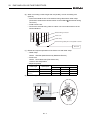
1
SAFETY PRECAUTIONS
(Read these precautions before using this product.)
Before using this product, please read this manual and the relevant manuals carefully and pay full attention
to safety to handle the product correctly.
In this manual, the safety precautions are classified into two levels: "
WARNING" and "
CAUTION".
WARNING
Indicates that incorrect handling may cause hazardous conditions,
resulting in death or severe injury.
CAUTION
Indicates that incorrect handling may cause hazardous conditions,
resulting in minor or moderate injury or property damage.
Under some circumstances, failure to observe the precautions given under "
CAUTION" may lead to
serious consequences.
Make sure that the end users read this manual and then keep the manual in a safe place for future
reference.
[DESIGN PRECAUTIONS]
WARNING
Create a safety circuit outside the programmable controller to ensure the whole system will operate
safely even if an external power failure or a programmable controller failure occurs. Otherwise,
incorrect output or malfunction may cause an accident.
(1) When creating an emergency stop circuit, a protection circuit or an interlock circuit for
incompatible actions such as forward/reverse rotation or for damage prevention such as the
upper/lower limit setting in positioning, create it outside the programmable controller.
Install the emergency stop switch outsid the controlpanel so that workers can operate it easily.
(2) When the programmable controller detects the following error conditions, it stops the operation
and turn off all the outputs.
• The overcurrent or overvoltage protector of the power supply module is activated.
• The programmable controller CPU detects an error such as a watchdog timer error by the
self-diagnostics function.
In the case of an error undetectable by the programmable controller CPU, such as an I/O control
part error, all the outputs may turn on. In order to make all machines operate safely in such a
case, set up a fail-safe circuit or a specific mechanism outside the programmable controller. For
fail safe circuit example, refer to "OADING AND INSTALLATION" of this manual.
(3) Depending on the failure of the output module's relay or transistor, the output status may remain
ON or OFF incorrectly. For output signals that may lead to a serious accident, create an external
monitoring circuit.
A-1
[DESIGN PRECAUTIONS]
WARNING
If load current more than the rating or overcurrent due to a short circuit in the load has flowed in the
output module for a long time, it may cause a fire and smoke. Provide an external safety device such
as a fuse.
Design a circuit so that the external power will be supplied after power-up of the programmable
controller.
Activating the external power supply prior to the programmable controller may result in an accident
due to incorrect output or malfunction.
For the operation status of each station at a communication error in data link, refer to the respective
data link manual.
Otherwise, incorrect output or malfunction may cause an accident.
When controlling a running programmable controller (data modification) by connecting a peripheral
device to the CPU module or a PC to a special function module, create an interlock circuit on
sequence programs so that the whole system functions safely all the time.
Also, before performing any other controls (e.g. program modification, operating status change
(status control)), read the manual carefully and ensure the safety.
In these controls, especially the one from an external device to a programmable controller in a
remote location, some programmable controller side problem may not be resolved immediately due
to failure of data communications.
To prevent this, create an interlock circuit on sequence programs and establish corrective
procedures for communication failure between the external device and the programmable controller
CPU.
When setting up the system, do not allow any empty slot on the base unit.
If any slot is left empty, be sure to use a blank cover (A1SG60) or a dummy module (A1SG62) for it.
When using the extension base unit, A1S52B(S1), A1S55B(S1) or A1S58B(S1), attach the included
dustproof cover to the module in slot 0.
Otherwise, internal parts of the module may be flied in the short circuit test or when an overcurrent or
overvoltage is accidentally applied to the external I/O section.
CAUTION
Do not install the control lines or communication cables together with the main circuit or power lines,
or bring them close to each other.
Keep a distance of 100mm (3.94inch) or more between them.
Failure to do so may cause malfunctions due to noise.
If having read register R outside the allowable range with the MOV instruction, the file register data
will be FFFFH. Using this as it is may cause malfunctions.Pay attention not to use any out-of-range
file register when designing sequence programs.For instruction details, refer to the programming
manual.
When an output module is used to control the lamp load, heater, solenoid valve, etc., a large current
(ten times larger than the normal one) may flow at the time that the output status changes from OFF
to ON. Take some preventive measures such as replacing the output module with the one of a
suitable current rating.
Time from when the CPU module is powered on or is reset to when it enters in RUN status depends
on the system configuration, parameter settings, and program size.
Design the program so that the entire system will always operate safely, regardless of the time.
A-2
[INSTALLATION PRECAUTIONS]
CAUTION
Use the programmable controller under the environment specified in the user's manual.
Otherwise, it may cause electric shocks, fires, malfunctions, product deterioration or damage.
Install the module after inserting the pegs on the bottom of the module securely into the base unit
peg holes.
Not doing so could cause a malfunction, failure or fall.
Tightening the screw excessively may damage the screw and/or the module, resulting in a drop of
the module, a short circuit or malfunctions.
Connect the extension cable to the connector of the base unit or module.
Check for incomplete connection after installing it.
Poor electrical contact may cause incorrect inputs and/or outputs.
Insert the memory card and fully press it to the memory card connector.
Check for incomplete connection after installing it.
Poor electrical contact may cause malfunctions.
Be sure to shut off all the phases of the external power supply used by the system before mounting
or removing the module.
Failure to do so may damage the module.
Do not directly touch the conductive part or electronic components of the module.
Doing so may cause malfunctions or a failure of the module.
A-3
[WIRING PRECAUTIONS]
WARNING
Be sure to shut off all phases of the external power supply used by the system before wiring.
Failure to do so may result in an electric shock or damage of the product.
Before energizing and operating the system after wiring, be sure to attach the terminal cover
supplied with the product.
Failure to do so may cause an electric shock.
CAUTION
Always ground the FG and LG terminals to the protective ground conductor.
Failure to do so may cause an electric shock or malfunctions.
Wire the module correctly after confirming the rated voltage and terminal layout.
Connecting a power supply of a different voltage rating or incorrect wiring may cause a fire or failure.
Do not connect multiple power supply modules to one module in parallel.
The power supply modules may be heated, resulting in a fire or failure.
Press, crimp or properly solder the connector for external connection with the specified tool.
Incomplete connection may cause a short circuit, fire or malfunctions.
Tighten terminal screws within the specified torque range.
If the screw is too loose, it may cause a short circuit, fire or malfunctions.
If too tight, it may damage the screw and/or the module, resulting in a short circuit or malfunctions.
Carefully prevent foreign matter such as dust or wire chips from entering the module.
Failure to do so may cause a fire, failure or malfunctions.
Install our programmable controller in a control panel for use.
Wire the main power supply to the power supply module installed in a control panel through a
distribution terminal block.
Furthermore, the wiring and replacement of a power supply module have to be performed by a
maintenance worker who acquainted with shock protection.
(For the wiring methods, refer to Section 19.7.)
A-4
[START AND MAINTENANCE PRECAUTIONS
WARNING
Do not touch any terminal during power distribution.
Doing so may cause an electric shock.
Correctly connect the battery connector.
Do not charge, disassemble, heat, short-circuit, solder, or throw the battery into the fire.
Incorrect battery handling may cause personal injuries or a fire due to exothermic heat, burst and/or
ignition.
Be sure to shut off all phases of the external power supply used by the system before cleaning or
retightening the terminal screws or module mounting screws.
Failure to do so may result in an electric shock.
If they are too loose, it may cause a short circuit or malfunctions.
Tightening the screw excessively may damage the screw and/or the module, resulting in a drop of
the module, a short circuit or malfunctions.
A-5
CAUTION
When performing online operations (especially, program modification, forced output or operating
status change) by connecting a peripheral device to the running CPU module, read the manual
carefully and ensure the safety.
Incorrect operation will cause mechanical damage or accidents.
Do not disassemble or modify each of modules.
Doing so may cause failure, malfunctions, personal injuries and/or a fire.
When using a wireless communication device such as a mobile phone, keep a distance of 25cm
(9.84inch) or more from the programmable controller in all directions.
Failure to do so may cause malfunctions.
Be sure to shut off all the phases of the external power supply used by the system before mounting
or removing the module.
Failure to do so may result in failure or malfunctions of the module.
Do not drop or apply any impact to the battery.
Doing so may damage the battery, resulting in electrolyte spillage inside the battery.
If any impact has been applied, discard the battery and never use it.
Do not install/remove the terminal block more than 50 times after the first use of the product.
(IEC 61131-2 compliant)
Before handling modules, touch a grounded metal object to discharge the static electricity from the
human body.
Failure to do so may cause failure or malfunctions of the module.
A-6
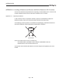
[DISPOSAL PRECAUTIONS]
CAUTION
When disposing of the product, treat it as an industrial waste.
When disposing of batteries, separate them from other wastes according to the local regulations.
(For details of the battery directive in EU member states, refer to Appendix 11.)
[TRANSPORTATION PRECAUTIONS]
CAUTION
When transporting lithium batteries, make sure to treat them based on the transportation regulations.
(Refer to Appendix 10 for details of the relevant models.)
A-7
CONDITIONS OF USE FOR THE PRODUCT
(1) Mitsubishi programmable controller ("the PRODUCT") shall be used in conditions;
i) where any problem, fault or failure occurring in the PRODUCT, if any, shall not lead to any major
or serious accident; and
ii) where the backup and fail-safe function are systematically or automatically provided outside of
the PRODUCT for the case of any problem, fault or failure occurring in the PRODUCT.
(2) The PRODUCT has been designed and manufactured for the purpose of being used in general
industries.
MITSUBISHI SHALL HAVE NO RESPONSIBILITY OR LIABILITY (INCLUDING, BUT NOT
LIMITED TO ANY AND ALL RESPONSIBILITY OR LIABILITY BASED ON CONTRACT,
WARRANTY, TORT, PRODUCT LIABILITY) FOR ANY INJURY OR DEATH TO PERSONS OR
LOSS OR DAMAGE TO PROPERTY CAUSED BY the PRODUCT THAT ARE OPERATED OR
USED IN APPLICATION NOT INTENDED OR EXCLUDED BY INSTRUCTIONS, PRECAUTIONS,
OR WARNING CONTAINED IN MITSUBISHI'S USER, INSTRUCTION AND/OR SAFETY
MANUALS, TECHNICAL BULLETINS AND GUIDELINES FOR the PRODUCT.
("Prohibited Application")
Prohibited Applications include, but not limited to, the use of the PRODUCT in;
• Nuclear Power Plants and any other power plants operated by Power companies, and/or any
other cases in which the public could be affected if any problem or fault occurs in the PRODUCT.
• Railway companies or Public service purposes, and/or any other cases in which establishment of
a special quality assurance system is required by the Purchaser or End User.
• Aircraft or Aerospace, Medical applications, Train equipment, transport equipment such as
Elevator and Escalator, Incineration and Fuel devices, Vehicles, Manned transportation,
Equipment for Recreation and Amusement, and Safety devices, handling of Nuclear or
Hazardous Materials or Chemicals, Mining and Drilling, and/or other applications where there is a
significant risk of injury to the public or property.
Notwithstanding the above, restrictions Mitsubishi may in its sole discretion, authorize use of the
PRODUCT in one or more of the Prohibited Applications, provided that the usage of the PRODUCT
is limited only for the specific applications agreed to by Mitsubishi and provided further that no
special quality assurance or fail-safe, redundant or other safety features which exceed the general
specifications of the PRODUCTs are required. For details, please contact the Mitsubishi
representative in your region.
A-8
REVISIONS
*The manual number is noted at the lower left of the back cover.
Print Date
*Manual Number
Sep.1996
SH (NA)-3599-A
Feb,1999
SH(NA)-3599-B
Revision
First printing
Additional model
SW
5
-GPPW GPP Function Software Package for Windows
Addition
The contents of the function version B has been added.
Section 2.2, Section 7.2, Sections 8.2.1, 8.2.2, Section 19.8, Appendix 7, 8
Partial correction
Safety Precautions, Contents, Section 1.2, Section 3.3.1, Chapter 4, Section
5.3, Section 6.1, Section 8.10.1, Section 15.2, Section 16.1, Section 19.7.1,
Section 21.3.1, Appendix 1.6, Appendix 2
Dec., 2002
SH(NA)-3599-C
Equivalent to Japanese version D
Partial correction
SAFETY PRECAUTIONS, Section 3.1.2, Section 3.3.1, Section 3.3.2, Section
3.3.3, Section 8.2.1, Section 8.5, Section 12.1.5, Section 12.1.6, Chapter 13,
Section 14.3, Section 15.1, Section 15.3, Section 16.1, Section 16.2, Section
17.2, Section 17.3, Section 19.1, Section 22.3.2, Appendix 3
Dec., 2003
SH(NA)-3599-D
Additional model
A1SY42P
Addition
Appendix 9, 9.1, 9.2
Partial correction
Section 3.3.1, Section 14.3, Section 18.3, Section 19.4.1, Section 19.8, Section
20.1.4, Section 21.3
Oct., 2006
SH(NA)-3599-E
Partial correction
SAFETY PRECAUTIONS, Section 1.1, Section 1.2, Section 2.1, 3.1.1, Section
3.1.2, Section 3.3.1, Section 3.3.2, Chapter 4, Section 5.3, Section 7.1, Section
7.2, Section 8.1, Section 8.2.1, Section 8.3, Section 8.4.3, Section 8.6, Section
8.8, Section 8.9, Section 8.10.1, Section 9.3, Section 9.4, Section 10.1, Section
10.5, Section 10.6.3, Section 10.8, Section 12.1, Section 12.1.3, Section 12.1.5,
Section 12.4, Chapter 13, Section 14.2, Section 15.1, Section 15.3, Section
16.1.1, Section 16.2, Section 16.3, Section 17.1, Section 17.2, Section 17.3,
Section 17.5, Section 18.1, Section 18.2, Section 18.3, Section 19.1, Section
19.4.1, Section 19.4.2, Section 19.5, Section 19.6, Section 19.7, Section 19.7.1,
Section 19.7.2, 20, Section 20.2.4, Section 20.2.6, Section 21.2, Section 21.3,
Section 21.4, Section 21.5, Section 22.2.5, Section 22.2.6, Section 22.2.8,
Section 22.3.3, Section 22.5.2, Appendix 1.1, Appendix 1.6, Appendix 2,
Appendix 3, Appendix 4.1, Appendix 4.2, Appendix 5.1, Appendix 5.2,
Deletion
Section 14.2
Chapter change
Section 14.3
Section 14.2
A-9
Print Date
*Manual Number
Apr.,2007
SH(NA)-3599-F
Revision
Partial correction
Section 3.1.1, 3.3.1, 3.3.2, 17.1, 19.7.1, 19.7.2, 20.1.3, 20.2.7, 22.5.1, 22.5.2,
Appendix 2, Appendix 3, Appendix 6.3
Addition
Section 20.1.8
Sep.,2008
SH(NA)-3599-G
Partial correction
SAFETY PRECAUTIONS, Section 5.2, 5.4, 8.2, 8.2.1, 8.5, 9.2, 9.3, 10.1, 10.3.
10.4, 10.5, 10.6.1, 12.1, 12.1.1, 12.1.7, 12.2, 12.3, 12.4, Chapter 13, Section
15.1, 15.3, 16.1.1, 16.2, 19.1, 19.2, 19.3, 19.4.1, 19.4.2, 19.7.1, 19.8, 20.1,
20.1.2, 20.1.3, 20.2, 20.2.1, 20.2.2, 20.2.3, 20.2.4, 20.2.6, 20.2.7, Chapter 21,
Section 21.3.1, 21.3.2, 21.4, 21.5, 22.1, 22.2.2, 22.2.5, 22.3, 22.5.1, Appendix 2
Addition
Appendix 11, Appendix 11.1, Appendix 11.2
Aug.,2009
SH(NA)-3599-H
Partial correction
Section 15.1, 18.3, 18.6, Chapter 20, Section 21.3.1, 21.3.2, 22.3.3, 22.5.1,
Appendix 2, 3
Nov.,2009
SH(NA)-3599-I
Partial correction
SAFETY PRECAUTIONS, Section 3.3.1, 21.3.1
Addition
CONDITIONS OF USE FOR THE PRODUCT
Mar.,2010
SH(NA)-3599-J
Partial correction
SAFETY PRECAUTIONS, Section 3.3.1, 3.3.2, 19.1, 19.7.1, 21.2, 21.3.2,
22.3.7, Appendix 2
Jan., 2011
SH(NA)-3599-K
Partial correction
Section 3.2, Section 15.1, Section 19.1, Section 20.1.1, Section 20.1.8
Addition
Section 20.1.9
Japanese Manual Version SH-3587-N
This manual does not imply guarantee or implementation right for industrial ownership or implementation of other rights.
Mitsubishi Electric Corporation is not responsible for industrial ownership problems caused by use of the contents of this
manual.
1996 MITSUBISHI ELECTRIC CORPORATION
A - 10
Introduction
Thank you for purchasing the Mitsubishi programmable logic controller MELSEC-QnA series.
Before using your new PLC, please read this manual thoroughly to gain an understanding of its functions so
that you can use it properly.
Please forward a copy of this manual to the end user.
Table of Contents
1
ABOUT THIS MANUAL
1.1
About this Manual..........................................................................................................................1 - 1
1.2
Abbreviations and Generic Terms Used in this Manual ................................................................1 - 2
2
OVERVIEW
2.1
Features ........................................................................................................................................2 - 1
2.2
3.1
3.2
3.3
2 - 1 to 2 - 8
Additional Functions of Q2ASCPU................................................................................................2 - 5
2.2.1
3
1 - 1 to 1 - 2
Overview of added functions.................................................................................................2 - 7
SYSTEM CONFIGURATION
3 - 1 to 3 - 23
System Configuration ....................................................................................................................3 - 1
3.1.1
Equipment configuration in a stand-alone system ................................................................3 - 1
3.1.2
Configuration of peripheral devices capable of Q2ASCPU...................................................3 - 2
System Configuration Overview ....................................................................................................3 - 3
System Equipment ........................................................................................................................3 - 5
3.3.1
System equipment list ...........................................................................................................3 - 5
3.3.2
Precautions when configuring the system...........................................................................3 - 19
3.3.3
Q2ASCPU memory block diagram......................................................................................3 - 23
4
PERFORMANCE SPECIFICATIONS
4 - 1 to 4 - 3
5
I/O NUMBER ASSIGNMENT
5.1
I/O Numbers ..................................................................................................................................5 - 1
5.2
I/O Number Assignment Concept..................................................................................................5 - 2
5.3
I/O Assignment with GPP Function ...............................................................................................5 - 4
5.4
Example of I/O Number Assignment .............................................................................................5 - 9
6
DATA COMMUNICATIONS WITH SPECIAL FUNCTION MODULES 6 - 1 to 6 - 5
6.1
Reading/Writing Data from/to the Q2ASCPU Using the FROM/TO Instruction ............................6 - 2
6.2
Reading/Writing Data from/to the Q2ASCPU Using Special Direct Devices.................................6 - 3
6.3
Processing for Data Communication Requests from a Special Function Module .........................6 - 5
7
AUTO REFRESH FUNCTION
7.1
For MELSECNET/MINI-S3............................................................................................................7 - 1
7.2
Auto Refresh Setting of CC-Link ...................................................................................................7 - 8
5 - 1 to 5 - 13
7 - 1 to 7 - 14
A - 11
8
DEBUGGING FUNCTION
8 - 1 to 8 - 64
8.1
Function List ..................................................................................................................................8 - 1
8.2
Monitor Function............................................................................................................................8 - 2
8.2.1
Monitoring condition setting ..................................................................................................8 - 2
8.2.2
Monitor test of local device (function version B or later) .....................................................8 - 12
8.3
Write During RUN........................................................................................................................8 - 15
8.4
Execution Time Measurement.....................................................................................................8 - 19
8.4.1
Program monitor list ............................................................................................................8 - 19
8.4.2
Interrupt program monitor list ..............................................................................................8 - 22
8.4.3
Scan time measurement .....................................................................................................8 - 23
8.5
Sampling Trace Function ............................................................................................................8 - 25
8.6
Status Latch Function..................................................................................................................8 - 35
8.7
Step Operation ............................................................................................................................8 - 41
8.7.1
Step execution ....................................................................................................................8 - 42
8.7.2
Partial execution..................................................................................................................8 - 44
8.7.3
Skip function........................................................................................................................8 - 47
8.8
Program Trace Function..............................................................................................................8 - 48
8.9
Simulation Function.....................................................................................................................8 - 57
8.10 Debugging by Several People.....................................................................................................8 - 61
8.10.1 Simultaneous monitoring by several people .......................................................................8 - 62
8.10.2 Simultaneous execution of write during RUN by several people ........................................8 - 63
9
MAINTENANCE FUNCTION
9 - 1 to 9 - 19
9.1
Function List ..................................................................................................................................9 - 1
9.2
Watchdog Timer ............................................................................................................................9 - 2
9.3
Self-diagnostics Function ..............................................................................................................9 - 4
9.3.1
Interruption due to error detection.........................................................................................9 - 8
9.3.2
LED inidcation due to an error ..............................................................................................9 - 8
9.3.3
Resetting error ......................................................................................................................9 - 9
9.4
Error History ................................................................................................................................9 - 10
9.5
System protect ............................................................................................................................9 - 11
9.6
Password Registration ................................................................................................................9 - 12
9.7
System Display............................................................................................................................9 - 14
9.8
LED indication .............................................................................................................................9 - 15
10
9.8.1
LED indication .....................................................................................................................9 - 15
9.8.2
Priority setting .....................................................................................................................9 - 17
OTHER FUNCTIONS
10 - 1 to 10 - 24
10.1 Function List ................................................................................................................................10 - 1
10.2 Constant Scan.............................................................................................................................10 - 2
10.3 Latch Function.............................................................................................................................10 - 5
10.4 Setting of the Output (Y) Status When Switching from STOP to RUN........................................10 - 7
10.5 Clock Function.............................................................................................................................10 - 8
10.6 Remote Operation .....................................................................................................................10 - 12
10.6.1 Remote RUN/STOP ..........................................................................................................10 - 12
10.6.2 Remote STEP-RUN ..........................................................................................................10 - 15
A - 12
10.6.3 Remote PAUSE ................................................................................................................10 - 16
10.6.4 Remote RESET.................................................................................................................10 - 18
10.6.5 Remote latch clear ............................................................................................................10 - 19
10.6.6 Relationship between remote operation and CPU module RUN/STOP key switch ..........10 - 20
10.7 Terminal Operation....................................................................................................................10 - 21
10.7.1 Operation for message display .........................................................................................10 - 21
10.7.2 Key input operation ...........................................................................................................10 - 22
10.8 Reading Module Access Time Intervals ....................................................................................10 - 23
11
COMMENTS THAT CAN BE STORED IN Q2ASCPU
11 - 1 to 11 - 8
11.1 Function List ................................................................................................................................11 - 1
11.2 PLC name ...................................................................................................................................11 - 2
11.3 Drive Title ....................................................................................................................................11 - 3
11.4 File Title.......................................................................................................................................11 - 4
11.5 Device Comment.........................................................................................................................11 - 5
11.6 Statements/Notes........................................................................................................................11 - 7
11.7 Initial Device Value Comment .....................................................................................................11 - 8
12
OVERVIEW OF PROCESSING PERFORMED BY THE Q2ASCPU12 - 1 to 12 - 28
12.1 Program Execution Types ...........................................................................................................12 - 1
12.1.1 Initial execution type programs ...........................................................................................12 - 4
12.1.2 Scan execution type program .............................................................................................12 - 7
12.1.3 Low-speed execution type program ....................................................................................12 - 9
12.1.4 Standby type program.......................................................................................................12 - 16
12.1.5 Initial processing ...............................................................................................................12 - 22
12.1.6 Refresh processing of I/O module.....................................................................................12 - 22
12.1.7 END processing ................................................................................................................12 - 23
12.2 Operation Processing of RUN, STOP, PAUSE, and STEP-RUN..............................................12 - 24
12.3 Operation Processing for Instantaneous Power Failure............................................................12 - 26
12.4 Data Clear Processing ..............................................................................................................12 - 27
13
PARAMETER LIST
13 - 1 to 13 - 10
14
SELECTING MEMORY CARD MODELS
14 - 1 to 14 - 4
14.1 Applications of Memory Cards ....................................................................................................14 - 2
14.2 Selecting Memory Card Capacity................................................................................................14 - 3
15
HARDWARE SPECIFICATIONS OF CPU MODULES
15 - 1 to 15 - 6
15.1 SPECIFICATIONS ......................................................................................................................15 - 1
15.2 Part Names .................................................................................................................................15 - 2
15.3 Relationship between Switch Operations and LEDs/LED Display ..............................................15 - 4
16
POWER SUPPLY MODULE
16 - 1 to 16 - 6
16.1 Specifications ..............................................................................................................................16 - 1
16.1.1 Power supply module specifications ...................................................................................16 - 1
A - 13
16.1.2 Power supply module selection...........................................................................................16 - 3
16.2 Precautions for Handling .............................................................................................................16 - 4
16.3 Part Names .................................................................................................................................16 - 5
17
BASE UNIT AND EXTENSION CABLE
17 - 1 to 17 - 9
17.1 Base Unit Specifications..............................................................................................................17 - 1
17.1.1 Main base unit for high-speed access (A1S38HB/A1S38HBEU)........................................17 - 2
17.2 Extension Cable Specification List ..............................................................................................17 - 3
17.3 Application Standards of Extension Base Unit (A1S52B(S1), A1S55B(S1), A1S58B(S1), A52B,
A55B, A58B)................................................................................................................................17 - 4
17.4 Handling Precautions ..................................................................................................................17 - 6
17.5 Part Names .................................................................................................................................17 - 7
18
MEMORY CARDS AND BATTERIES
18 - 1 to 18 - 9
18.1 Memory Card Specifications .......................................................................................................18 - 1
18.2 Handling Memory Cards..............................................................................................................18 - 3
18.3 Battery Specifications (CPU Module and Memory Card Batteries) .............................................18 - 4
18.4 Handling Precautions ..................................................................................................................18 - 5
18.5 Part Names of Memory Card.......................................................................................................18 - 6
18.6 Installing Batteries (CPU Module and Memory Card Batteries) ..................................................18 - 7
18.7 Installing/Removing A Memory Card...........................................................................................18 - 8
19
LOADING AND INSTALLATION
19 - 1 to 19 - 19
19.1 Fail-Safe Circuit Concept ............................................................................................................19 - 1
19.2 Installation Environment ..............................................................................................................19 - 6
19.3 Calculation of Heat Generated by the programmable controller .................................................19 - 7
19.4 Installing the Base Units..............................................................................................................19 - 9
19.4.1 Installation precautions .......................................................................................................19 - 9
19.4.2 Installation .........................................................................................................................19 - 10
19.5 Installation and Removal of Modules ........................................................................................19 - 11
19.6 Installation and Removal of the Dustproof Cover......................................................................19 - 13
19.7 Wiring ........................................................................................................................................19 - 15
19.7.1 Wiring instructions.............................................................................................................19 - 15
19.7.2 Wiring to module terminals................................................................................................19 - 18
19.8 Precautions When Connecting Uninterruptible Power Supply Module (UPS)...........................19 - 19
20
EMC AND LOW VOLTAGE DIRECTIVES
20 - 1 to 20 - 16
20.1 Requirements for Compliance with EMC Directives....................................................................20 - 1
20.1.1 EMC Directive related standards ........................................................................................20 - 1
20.1.2 Installation inside the control panel .....................................................................................20 - 3
20.1.3 Cables .................................................................................................................................20 - 4
20.1.4 Power supply module..........................................................................................................20 - 9
20.1.5 Base unit .............................................................................................................................20 - 9
20.1.6 Ferrite core........................................................................................................................20 - 10
20.1.7 Noise filter (power supply line filter) ..................................................................................20 - 11
20.1.8 Power line for external power supply terminal ..................................................................20 - 12
A - 14
20.1.9 Installation environment of the CC-Link/LT module and the AS-i module.........................20 - 12
20.2 Requirements for Compliance with Low Voltage Directives......................................................20 - 13
20.2.1 Standard applied for MELSEC-QnA series programmable controller ...............................20 - 13
20.2.2 Precautions when using the QnA series programmable controller ...................................20 - 13
20.2.3 Power supply.....................................................................................................................20 - 14
20.2.4 Control panel.....................................................................................................................20 - 15
20.2.5 Module installation ............................................................................................................20 - 16
20.2.6 Grounding .........................................................................................................................20 - 16
20.2.7 External wiring...................................................................................................................20 - 16
21
MAINTENANCE AND INSPECTION
21 - 1 to 21 - 16
21.1 Daily Inspection ...........................................................................................................................21 - 1
21.2 Periodic Inspection ......................................................................................................................21 - 2
21.3 Battery Replacement...................................................................................................................21 - 3
21.3.1 Battery life ...........................................................................................................................21 - 5
21.3.2 Battery replacement procedure.........................................................................................21 - 11
21.4 When Reoperating a programmable controller After Storing it with a Battery Unconnected.....21 - 15
21.5 When a programmable controller is Reoperated After Stored with the Battery Over the Battery Life
..................................................................................................................................................21 - 16
22
TROUBLESHOOTING
22 - 1 to 22 - 53
22.1 Fundamentals of Troubleshooting...............................................................................................22 - 1
22.2 Troubleshooting...........................................................................................................................22 - 2
22.2.1 Troubleshooting flowchart ...................................................................................................22 - 2
22.2.2 Flow for actions when the "POWER" LED is turned OFF ...................................................22 - 3
22.2.3 Flow for actions when the "RUN" LED is turned OFF .........................................................22 - 4
22.2.4 When the "RUN" LED is flashing ........................................................................................22 - 5
22.2.5 Flow for actions when the "ERROR LED" is turned ON/flashing ........................................22 - 6
22.2.6 When the "USER" LED is turned ON ..................................................................................22 - 7
22.2.7 Flow for actions when the "BAT.ARM" LED is turned ON...................................................22 - 7
22.2.8 Flow for actions when the output module's output load does not turn ON ..........................22 - 8
22.2.9 Flow for actions when the program cannot be written.........................................................22 - 9
22.2.10 Flow for actions when booting from a memory card is not possible..................................22 - 11
22.2.11 Flow chart used when the CPU module is not started up .................................................22 - 13
22.3 Error Code List ..........................................................................................................................22 - 15
22.3.1 Error Codes.......................................................................................................................22 - 16
22.3.2 Procedure to read an error code .......................................................................................22 - 16
22.3.3 Error code list (1000 to 1999)............................................................................................22 - 17
22.3.4 Error code list (2000 to 2999)............................................................................................22 - 22
22.3.5 Error code list (3000 to 3999)............................................................................................22 - 28
22.3.6 Error code list (4000 to 4999)............................................................................................22 - 32
22.3.7 Error code list (5000 to 5999)............................................................................................22 - 41
22.3.8 Error code list (6000 to 6999)............................................................................................22 - 42
22.3.9 Error code list (7000 to 10000)..........................................................................................22 - 44
22.3.10 Canceling of Errors ...........................................................................................................22 - 45
22.4 Resetting Errors ........................................................................................................................22 - 46
22.5 Fault Examples with I/O Modules..............................................................................................22 - 47
A - 15
22.5.1 Faults with the input circuit and the corrective actions......................................................22 - 47
22.5.2 Faults in the output circuit .................................................................................................22 - 49
APPENDICES
APPENDIX 1
App - 1 to App - 165
INSTRUCTION LIST ................................................................................................. App - 1
Appendix 1.1
Sequence Instructions ......................................................................................... App - 1
Appendix 1.2
Basic Instructions................................................................................................. App - 5
Appendix 1.3
Application Instructions ...................................................................................... App - 17
Appendix 1.4
Data Link Instructions ........................................................................................ App - 38
Appendix 1.5
PID Control Instructions ..................................................................................... App - 41
Appendix 1.6
Special Function Module Instructions ................................................................ App - 42
APPENDIX 2
Special Relay List ................................................................................................... App - 48
APPENDIX 3
Special Register List ............................................................................................... App - 72
APPENDIX 4
PRECAUTIONS FOR UTILIZING THE EXISTING MELSEC-A SERIES PROGRAM FOR
Q2ASCPU............................................................................................................. App - 110
Appendix 4.1
Instructions....................................................................................................... App - 110
Appendix 4.2
Device .............................................................................................................. App - 118
Appendix 4.3
Parameters ...................................................................................................... App - 120
Appendix 4.4
Timer and Interrupt Counter Operations .......................................................... App - 121
Appendix 4.5
Sequence Programs, Statements, Notes......................................................... App - 122
Appendix 4.6
Microcomputer programs ................................................................................. App - 124
Appendix 4.7
Comments........................................................................................................ App - 125
Appendix 4.8
Constant Scan Function, Error Check Function............................................... App - 126
Appendix 4.9
I/O control mode .............................................................................................. App - 127
Appendix 4.10 Data Link System............................................................................................. App - 128
Appendix 4.11 Index Register Processing ............................................................................... App - 129
Appendix 4.12 CHK Instruction, IX Instruction......................................................................... App - 130
Appendix 4.13 Accessing File Register R with Instructions ..................................................... App - 131
APPENDIX 5
ERROR CODES RETURNED TO THE REQUEST SOURCE IN GENERAL DATA
PROCESSING ...................................................................................................... App - 132
Appendix 5.1
Error Codes...................................................................................................... App - 132
Appendix 5.2
Error Contents of Error Codes Detected by the CPU Module (4000H to 4FFFH)
......................................................................................................................... App - 133
APPENDIX 6
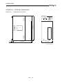
EXTERNAL DIMENSIONS ................................................................................... App - 141
Appendix 6.1
Q2AS(H)CPU(S1) module ............................................................................... App - 141
Appendix 6.2
A1S61PN, A1S62PN and A1S63P power supply modules ............................. App - 142
Appendix 6.3
Main Base Unit................................................................................................. App - 143
Appendix 6.4
Extension Base Unit......................................................................................... App - 145
APPENDIX 7
USE OF LOCAL DEVICE FOR SUBROUTINE/INTERRUPT PROGRAM STORAGE FILE
(FUNCTION VERSION B OR LATER) ................................................................. App - 151
APPENDIX 8
NETWORK RELAY FROM ETHERNET MODULE
(FUNCTION VERSION B OR LATER) ................................................................. App - 155
APPENDIX 9
Q2AS(H)CPU(S1) PROCESSING TIME .............................................................. App - 158
Appendix 9.1
Overview of the Q2AS(H)CPU(S1) Scan Time................................................ App - 158
Appendix 9.2
Causes of Increasing Scan Time ..................................................................... App - 159
APPENDIX 10 TRANSPORTATION PRECAUTIONS .................................................................. App - 162
Appendix 10.1 Relevant Models .............................................................................................. App - 162
A - 16
Appendix 10.2 Transportation Guidelines................................................................................ App - 163
APPENDIX 11 Handling of Batteries and Devices with Built-in Batteries in EU Countries ........... App - 164
Appendix 11.1 Disposal precautions........................................................................................ App - 164
Appendix 11.2 Exportation precautions ................................................................................... App - 165
INDEX
Index - 1 to Index - 5
A - 17
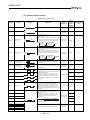
ABOUT THIS MANUAL
The following are manuals related to this product.
Request for the manuals as needed according to the chart below.
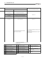
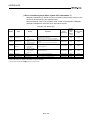
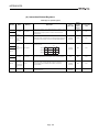
RELATED MANUALS
Manual No.
Manual Name
(Type code)
QnACPU GUIDEBOOK
For the first-time user of QnACPU, describes steps on creating a program, writing the program in
IB-66606
the CPU module, and debugging. Describes usage of QnACPU features.
(13JF10)
(Sold separately)
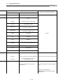
QnACPU PROGRAMMING MANUAL (Fundamentals)
Describes programming methods, device names and program types that are necessary in program
IB-66614
creation.
(13JF46)
(Sold separately)
QnACPU Programming Manual (Common Instructions)
Describes how to use sequence instructions, basic instructions and application instructions.
(Sold separately)
QnACPU PROGRAMMING MANUAL (Special Functions)
SH-080810ENG
(13JW11)
IB-66616
Describes dedicated instructions used in special-function modules.
(Sold separately)
QnACPU PROGRAMMING MANUAL (AD57 Instructions)
Describes dedicated instructions used to control theA D57(S1)-type CRT controller module.
(Sold separately)
QCPU (Q mode)/QnACPU PROGRAMMLNG MANUAL (PID Control Instructions)
Describes dedicated instructions used for PID control in Q2ACPU(S1), Q3ACPU and Q4ACPU.
(Sold separately)
(13JF48)
IB-66617
(13JF49)
SH-080040
(13JF59)
QCPU (Q mode)/QnACPU PROGRAMMING MANUAL (SFC)
Describes system components, performance specifications, functions, programming debug going
and error codes of MELSAP
SH-080041
(13JF60)
(Sold separately)
AnS Module Type I/O User's Manual
IB-66541
Describes specification of AnS module as I/O module.
(Sold separately)
Type QnA/Q4AR MELSECNET/10 Network System Reference Manual
(13JE81)
IB-66620
Descrlbes MELSECNET/10 overview, specifications, part names and settings.
(Sold separately)
Type MELSECNET, MELSECNET/B Data Link System Reference Manual
Describes MELSECNET(II) and MELSECNET/B overview, specifications, part names and settings.
(Sold separately)
(13JF77)
IB-66350
(13JF70)
GX Developer Version 8 Operating Manual
Describes the online functions of GX Developer including the programming procedure, printing out
procedure, and debugging procedure.
SH-080373
(13JU41)
(Included with product)
Type SW2IVD-GPPQ GPP Software package OPERATING MANUAL (Offline)
Describes SW2IVD-GPPQ's offline functions such as program creation, printout method and file
IB-66774
maintenance.
(13J921)
(Included with product)
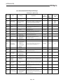
A - 18
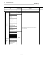
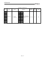
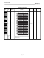
Manual No.
Manual Name
(Type code)
Type SW2IVD-GPPQ GPP Software package OPERATING MANUAL (Online)
Describes SW2IVD-GPPQ's online functions such as monitoring and debugging methods.
(Included with product)
IB-66775
(13J922)
Type SW2IVD-GPPQ GPP Software package OPERATING MANUAL (SFC)
Describes MWLSAP-3 system components, performamce specifications, functions, system start-up
IB-66776
procedure, SFC program editing method, monitoring method, printout method and error messages.
(13J923)
(Included with product)
Type SW2IVD-GPPQ GPP Software package OPERATING MANUAL (Q6TEL)
IB-66777
Describes Q6TEL system configuration, operating methods, etc.
(Included with product)
A - 19
(13J924)
USER PRECAUTONS
PRECAUTIONS WHEN USING THE QNA SERIES
When using a CPU module, format the memory using a peripheral device.
For details of memory format, refer to the following manuals.
• GX Developer Operating Manual
• SW
IVD-GPPQ Software package Operating Manual (Online)
PRECAUTIONS FOR BATTERY
(1)
The operation after removal of a battery
After removing a battery of the CPU module, format the memory using a peripheral
device to start next operation. (Refer to Section 21.4)
(2)
The operation after excess of a battery life
After removing a battery of the CPU module due to its excess life, format the memory
using a peripheral device to start next operation. (Refer to Section 21.5)
A - 20
1.
ABOUT THIS MANUAL
1
ABOUT THIS MANUAL
1.1
About this Manual
This manual serves to explain the specifications and functions of the Q2ASCPU,
Q2ASCPU-S1, Q2ASHCPU and Q2ASHCPU-S1 (abbreviated as Q2ASCPU hereafter),
the specifications of other modules, and the maintenance required for smooth system
operation, to users of MELSEC-QnA series programmable controllers.
It is divided into the following three main parts:
(1) Sections 2 and 3 These sections give the general description and system
configuration for the Q2ASCPU.
Read them to learn the features of Q2ASCPU, and the modules
that can be used and points to note when configuring a system.
(2) Sections 4 to 15 These sections give the specifications and functions of
Q2ASCPU.
They describe each Q2ASCPU function to enable you to use the
Q2ASCPU effectively.
(3) Sections 16 to 18 These sections describe the specifications and handling of units/
modules other than the CPU module (power supply module, base
units, etc.)
Read them to learn how to handle the power supply module, base
units, memory cards, etc.
(4) Section 19 to 20 These section describes the loading and installation, EMC and
low voltage directives.
(5) Section 21 to 22 These sections describe all aspects of maintenance, from
installing the Q2ASCPU to daily inspections and troubleshooting.
Read them to learn how to install the Q2ASCPU so as to ensure
smooth operation, and how to carry out daily inspections and
corrective action in the event of trouble.
REMARK
This manual does not cover MELSECNET(II) data link systems, MELSECNET/B data
link systems, MELSECNET/10 networks, or the SFC function.
For details on each function, refer to the following manuals.
• MELSECNET(II), MELSECNET/B Data Link
MELSECNET, MELSECNET/B Data Link System Reference Manual
• MELSECNET/10 Network
MELSECNET/10 Network System Manual for QnA/Q4AR
• SFC Function
QCPU (Q Mode)/QnACPU Programming Manual (SFC)
1-1
1.
ABOUT THIS MANUAL
1.2
Abbreviations and Generic Terms Used in this Manual
The following abbreviations and generic terms are used in this manual.
(1)
Q2ASCPU................................... Abbreviation for Q2ASCPU, Q2ASCPU-S1,
Q2ASHCPU, and Q2ASHCPU-S1 type CPU
modules.
(2)
Network module......................... Abbreviation of A1SJ71QLP21, and
A1SJ71QBR11 type MELSECNET/10 network
modules.
(3)
Ethernet module......................... Abbreviation of A1SJ71QE71N-B2 and
A1SJ71QE71N-B5T type Ethernet interface
modules.
(4)
Serial communication module.... Abbreviation of A1SJ71QC24(N),
A1SJ71QC24(N)-R2 type serial communication
module.
(5)
CC-Link.....................................
Abbreviation of Control & Communication Link
(6)
GPP function.............................
Abbreviations for the SW IVD-GPPQ type
GPP function software package, GX Developer.
(7)
Personal computer..................... IBM's PC/AT or completely compatible
computers.
(8)
Peripheral device capable ......... Generic term for a peripheral device capable of
of GPP functions
running the GPP function software, for example
an IBM PC/AT.
(9)
Q6PU......................................... Abbreviation for Q6PU programming unit.
(10) Peripheral device........................ Generic term for a device that is connected to a
QnACPU and can be used to operate it, for
example a personal computer or Q6PU.
(11) Built-in RAM............................... A RAM incorporated in the Q2AS CPU that
stores sequence programs and other data.
(12) Memory card.............................. Abbreviation for Q1MEMcard
type memory
(13) ACPU......................................... Generic term for a MELSEC-A series
programmable controller
1-2
2.
OVERVIEW
2
OVERVIEW
2.1
Features
Q2ASCPU has the following features.
(1)
Large memory capacity
(a) Q2AS(H)CPU-S1 has a program capacity of 60k steps, which means that 60k
steps can be used for a single program (Q2AS(H)CPU: 28k steps).
(b) The device memory capacity is 29k words and the user can change the number
of points as required.
For example, the default number of points for internal relays (M) is 8k points, but
this can be expanded up to 32k points.
(c) One memory card of a maximum of 2M bytes can be installed.
Memory cards are used to store programs, comments, statements, and file
registers.
(Programs can be stored in the CPU module itself, so a memory card is not
essential to run a CPU module.)
(2)
High-speed processing
(a) Higher operation processing speeds have been achieved for basic instructions
and application instructions.
A2USCPU(S1)
Q2ASHCPU(S1)
0.2 s
0.075 s
Application instructions 1.2 s
0.225 s
Basic instructions
(b) The access time for expansion data memory (file registers: R) has been
conformed with the internal devices of the Q2ASCPU (data registers: D, and link
registers: W).
(c) Reading/writing of the buffer memories of special function modules dedicated to
QnA (serial communication modules) have been realised processing speed-up
by six times compared to AnUCPU.
(The processing speed of the existing special function modules for ACPU use is
about the same as that when using AnUCPU.)
(d) A high-speed access base unit (A1S38HB/A1S38HBEU) is available to speed
up the processing time for accessing special function modules such as network
modules and serial communication modules that handle large quantities of data.
Simply by mounting the special function module on the high-speed access base
unit, the access processing speed is increased when the Q2ASCPU accesses
the special function module.
2-1
2.
OVERVIEW
(3)
Selection of program execution type that is appropriate for the control has been
realised.
There are four program execution types to be selected as follows.
(a) Initial execution type
This program type is executed once only when the Q2ASCPU is set to RUN.
(b) Scan execution type
This program type is run continually while the Q2ASCPU is in the RUN status.
This is equivalent to a conventional program that runs from step 0 to END
instruction.It is possible to create subroutine programs and interrupt programs
for this type of program.
(c) Low-speed execution type
This is a program type which is executed only during the surplus constant scan
time (process to preset the program execution time for constant scan time) or
during the set execution time of the low-speed execution program.
(d) Stand-by type
This type of program consists entirely of a subroutine program or interrupt
program.
(4)
The SFC language MELSAP3 has been supplied.
With enhancement of step attributes and SFC control instructions, MELSAP3 makes
SFC programming even easier.
(5)
A software development environment that improves program productivity has been
realized.
(a) In order to enable the design of structured programs, a file format has been
adopted for programs.
What would conventionally have been a single continuous program can now be
handled in a structured way as a number of files.
This allows for design work to be shared by several designers, and allows
management of programs in accordance with functions, processes, or
designers, etc.
2-2
2.
OVERVIEW
(b) The user can standardize and simplify programs by creating and using macro
instructions corresponding to functions.
(c) Devices can be used without restrictions.
1) Word device bit operations are possible.
2) Differential contacts can be used.
3) Buffer memories of special function modules can be accessed directly from a
program as devices.
4) The link data of network modules can be accessed directly from a program as
devices.
(d) Ease of operation for GPP function program editing has been improved.
1) Up to four programs, data, etc., can be edited simultaneously.
Programs and data can be cut and pasted between edited objects.
2) Ladder editing is possible while the ladder is displayed with comments.
3) Familiar operations can be performed with pull-down menus and dialog
boxes.
(e) The debugging function at start-up has been perfected.
1) Ladder modification while performing monitoring is possible.
2) Coil ON/OFF causes can be searched for.
3) The timing for monitoring can be set using a step number or device status,
allowing debugging to be conducted under the optimum conditions.
4) Devices for which index qualifications have been set can be monitored.
(f) The GPP function document creation function has been strengthened.
1) Since comments can now comprise 32 characters, they can be more detailed
than before.
2) Comments can now be set for all devices.
3) The statements and notes appended to programs can now be managed as
an integral part of the program, which makes program modifications and
utilization easier.
4) Printout data can be stored in a file.
2-3
2.
OVERVIEW
(g) A powerful array of support software packages is available for program creation.
1) Data conversion package
Comment data, device data, etc., which is created with spreadsheet software
and text editors available on the market, can be converted to files for GPP
function use.
Conversely, files created for GPP function use can be converted to data for
spreadsheets or text editors.
2) Macro/library package
The basic programs for accessing special function modules, and standard
programs for error detection, alarm processing, etc., have been brought
together as a package of macro and library data.
3) Ladder sequence linking package
This package is used to link multiple programs to make a single program.
This has an automatic allocation function that ensures that devices from each
program without duplicating in the created program.
4) CAD interface program
This package is used to handle sequence ladders, instruction lists, comment
data and SFC diagrams as CAD data and communicate these data to CAD
systems.
2-4
2.
OVERVIEW
2.2
Additional Functions of Q2ASCPU
New functions and instructions for special function module are added to the Q2ASCPU.
[Additional functions]
Variety of local devices................................................ Refer to Section 2.2.1 (1)
Monitor test of local device................................. Refer to Section 8.2.2
Use of local device at the subroutine/interrupt
program storage destination................................ Refer to Appendix 7
Auto refresh setting of CC-Link..................................... Refer to Section 2.2.1 (2),
Section 7.2.
MELSECNET/10 relay communication from the
Ethernet module (Network relay)................................... Refer to Section 2.2.1 (3),
Appendix 8.
Addition of AJ71QC24N-compatible commands
..................................................................................... Section 2.2.1 (4)
[Added instructions for special function module]
The following instructions have been added for function version "B" of the Q2ASCPU:
A1SJ61QBT11 control instructions ................................ 13
A1SD75 control instructions .......................................... 19
A1SJ71ID
-R4 control instructions .............................. 12
A1SJ71QE71 control instructions .................................. 10
Additional function/special function module instructions can be used for the Q2ASCPU
described function version B in the date column of the rating plate.
Check that function version B is described on the Q2ASCPU rating plate before using the
additional function/special function module instructions.
If your Q2ASCPU does not have indication of function version B, skip this item and the
description of additional functions.
When using additional function/special function module instructions of the Q2ASCPU, it is
necessary to match the GPP function model and the function version/version of the
applicable special function module. (Refer to Table 2.1.)
2-5
2.
OVERVIEW
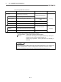
Table 2.1 List of combination between Q2ASCPU and function version/version of special function module
QnACPU
SW0IVDGPPQ
SW1IVDGPPQ
SW2IVDGPPQ
A1SJ71QE7
1(B2), (B5)
A1SD75PS3
9707B and
later
–
ÑüÑü
9707B and
later
–
–
No
restriction
No
restriction
–
A1SJ71
A1SJ61QBT
11
A1SJ71QC2
4(N)(R2)
–
9707B and
later
–
No
restriction
BC and later
–
No
restriction
–
–
–
–
–
–
–
–
–
–
–
–
–
–
–
–
–
–
MELSECNET/10 relay
communication from Ethernet
–
–
–
–
A1SJ71QE71 control instruction
–
–
–
–
–
–
–
–
–
Module/package Name
Function version
ID
-R4
Condition
Version
Local device
monitor test
Local device switching of
subroutine/interrupt program
–
Auto refresh function of CC-Link
A1SJ61QBT11 control
instructions
A1SD75 control instructions
–
ID interface module
instructions
–
–
–
–
Compatibility with A1SJ71QC24N
commands
–
–
–
REMARK
1) Marks
, -,
and
in Table 2.1 indicate as follows:
: Essential for use of function and instruction
–:
Irrelevant to function and instruction
: Required in the case of access to the QnACPU in other stations from
the peripheral device via Ethernet
: Not available on peripheral devices.
2) GX Developer supports functions of function version B.
2-6
2.
2.2.1
OVERVIEW
Overview of added functions
This section shows an overview of the added functions.
(1)
Variety of local device
(a) The device set as the local device at "Device" in Parameter can be monitored
and tested with a peripheral device.
This function allows checking and debug of the local device in the program
monitored with a peripheral device.
(b) The local device of the file where the subroutine program/interrupt program is
stored has made it possible to be used during execution of the subroutine
program/interrupt program.
For this function, even if an operation using the local device of the subroutine
program is carried out, the original local device cannot be overwritten. In
addition, even if an operation using the local device of the interrupt program, the
local device which is executed before starting up the interrupt program cannot be
overwritten.
(c) The following GPP function software packages are required to perform the
monitor test of the local device:
• Personal computer
GX Developer, SW
(2)
IVD-GPPQ type GPP function software package
Auto Refresh Setting of CC-Link
(a) When setting auto refresh of the CC-Link on the peripheral function, cyclic
communication with other stations connected to the CC-Link can be
automatically performed according to the set auto refresh data.
• Remote I/O station (Communication in ON/OFF data)
• Remote device station (Communication in ON/OFF data and Word data)
• Intelligent device station (Communication in ON/OFF data and Word data)
• Local station/master station (Communication in ON/OFF data and Word data)
The auto refresh setting of the CC-Link allows communication with other stations
using the FROM/TO instruction without communicating with the master station of
the CC-Link.
(b) Auto refresh is available for up to 8 CC-Link modules for each unit of Q2ASCPU.
Communication for 9th CC-Link modules and more can be performed with the
CC-Link module using the FROM/TO instruction.
(c) The following GPP function software packages are required to perform the auto
refresh setting of the CC-Link:
• Personal computer
GX Developer, SW IVD-GPPQ type GPP function software package
It is necessary to upgrade the master station local station module of CC-Link to
function version B or later.
2-7
2.
OVERVIEW
(3)
Netwotk relay from Ethernet module
(a) In the network system with mixture of Ethernet and MELSECNET/10, data can
be communicated with the Q2ASCPU of other stations via multiple Ethernets or
MELSECNET/10 modules.
(b) For the network relay from the Ethernet module, the function version of the
Ethernet module should be upgraded to "B" or later.
(4)
A1SJ71QC24N-compatible commands are possible.
(a) The following A1SJ71QC24N commands are available:
• Multiple blocks batch read: Command "0406"
• Multiple blocks batch write: Command "1406"
(b) Multiple blocks batch read/batch write is available with A1SJ71QC24N(-R2, R4).
Multiple blocks batch read/batch write is not available with A1SJ71QC24(-R2,
R4).
For commands of multiple blocks batch read/batch write, refer to the following
manual:
• Corresponding Additional Explanation for A1SJ71QC24N [-R2/R4]
2-8
3.
SYSTEM CONFIGURATION
3
SYSTEM CONFIGURATION
This section describes the system configurations that can be used for a system centered
on a Q2ASCPU, cautions on configuring the system, and the system equipment.
3.1
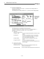
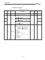
System Configuration
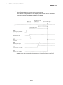
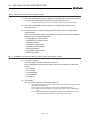
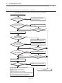
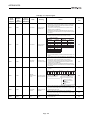
The following shows the configuration of equipment and peripheral device when a
Q2ASCPU is used in a stand-alone system.
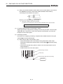
3.1.1
Equipment configuration in a stand-alone system
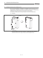
*1
Q1MEMMemory card
(optional)
Q2ASCPU
A1SC
NB
Extension cable
(building-block type)
A1S3 B/A1S38HB
Main base
A6BAT
Battery
A1S6 P(N) power supply
module
A1SX
input module
A1SY
output module
Special-function module
*2
A6 B extension base
(with power supply module)
A5 B extension base
(without power supply module)
A1SC
B
Extension cable
*2
A6 P power supply module
AX
input module
AY
output module
Special-function module
A1S6 B (S1) extension base
(with power-supply module)
A1S5 B (S1) extension base
(without power supply module)
A1S6 P(N) power supply
module
A1SX
input module
A1SY
output module
Special-function module
POINT
*1 Up to one memory card can be installed, if required.
SRAM and E2PROM memory cards allow file read/write when mounted on the
CPU module.
*2 When using an A1S5 B(S1), A5 B extension base unit, pay particular
attention to the power supply capacity of the main base unit.In the case of I/O
modules and the special function module with a high internal current
consumption, mounting on an A1S6 B(S1), A6 extension base unit is
recommended.
(Refer to Section 16.1 and Section 17.3 for details.)
3-1
3.
3.1.2
SYSTEM CONFIGURATION
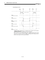
Configuration of peripheral devices capable of Q2ASCPU
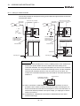
(To RS-422 interface)
Q2ASCPU
AC30R4-PUS cable
Q6PU
AC20R4-A8PU cable
programming unit
*2
RS-422 cable
RS-422
RS-232C
convertor
RS-232C cable
IBM-PC/AT-compatible
software package used:
*3
(Mounted to the
base unit)
A1SJ71QC24 serial
communication module
(To option board slot)
Option board
IC memory card
Dedicated cable
*1
(To RS-422 interface/RS-232C)*2
reader/writer
IBM-PC/AT-compatible
software package used:
RS-232C cable
*1
For details on the IC memory card reader/writer setting, refer to Operating Manual for the
peripheral device capable of GPP functions.
*2
*3
For connection to RS-422 interface, use the RS-422
/RS-232C converter.
When connecting the serial communication module and the peripheral devices capable of
GPP function, see User's Manual of the serial communication modules.
REMARK
1.
2.
For details on the system configuration for each peripheral device, refer to
the Operating Manual for each.
Q2ASCPU can connect a peripheral device capable of ACPU only when
accessing an ACPU in another station via a MELSECNET/10 or
MELSECNET data link. (However, Q2ASCPU cannot be accessed.) In
this case, set SW1 of system setting switch 2 on the CPU module ON.
3-2
3.
SYSTEM CONFIGURATION
3.2
System Configuration Overview
(a) Q2ASCPU, Q2ASHCPU system
[When the A1S6
B(S1), A1S5
B(S1) extension
[When the A6
B, A5
B extension base is used]
base is used]
The following shows an example that the 32-point
The following shows an example that the 16-point
module is installed to each slot.
module is installed to each slot.
System configuration
CPU module
Power supply
module
Main base
unit
(A1S38B)
Slot No.
0
1
2
3
5
4
6
7
00 20 40 60 80 A0 C0 E0
to
to
to
to
to
to
to
to
1F 3F 5F 7F 9F BF DF FF
Extension cable
Slot No.
1st extension
stage
1
2
3
4
5
6
7
Power supply
module
UNIT
1
2
3
4
5
6
7
8
9
10 11 12 13 14 15
100 120 140 160 180 1A0 1C0 1E0
to
to
to
to
to
Extension base unit (for A
Maximum number of
3rd extension stage
extension stages
to
N, A
A)
16 modules
I/O modules
Maximum number of
512 points
I/O points
Main base unit model
A1S32B, A1S33B, A1S35B, A1S38B, A1S38HB, A1S38HBEU
name
model name
to
1st extension stage
Maximum number of
Extension base unit
to
11F 13F 15F 17F 19F 1BF 1DF 1FF
A1S65B(S1), A1S68B(S1), A1S52B(S1),
A62B, A65B, A68B, A52B, A55B, A58B
A1S55B(S1), A1S58B(S1)
Extension cable
A1SC03B, A1SC07B, A1SC12B, A1SC30B,
model name
A1SC01B (right-side installation), A1SC60B
(1) Only one A6
B, A5
A1SC05NBA1SC07NBA1SC30NBA1SC50NB
B extension base can be used.(The second extension module cannot be used.)
(2) When the extension base A1S52B(S1), A1S55B(S1), A58B(S1) or A52B, A55B, A58B are used, the 5VDC
power is supplied from the power supply module of the main base unit.Before use, refer to Section 17.3 and
Precautions
examine if it can be used.
(3) Limit the length of extension cable to 6m (236inch) or shorter.
(4) When using the extension cable, do not install it with the main circuit cables, which has high voltage, large
current, or install them close together.
(1) Assign I/O numbers to the main base unit first, then to the extension base unit.
(2) Assign I/O numbers as if both main base unit and extension base unit have 8 slots each.When the A1S32B/
I/O number
assignment
(When I/O assignment is
not performed)
A1S33B/A1S35B for 2/3/5 slots are used as the main base unit, add 6/5/3 slots (96 points/80 points/48
points) and assign the extension base unit I/O numbers.
(3) 16 points are assigned to an empty slot.
(4) When A6
B or A5
B is used, be sure to set to a single extension level.If it is set to the number of skipped
stages, 16 points/slot are assigned to all of skipped stages 8 slots, and thus it does not work.
(5) Items (2) to (3) can be changed by the I/O assignment. (Refer to Section 5.3)
3-3
3.
SYSTEM CONFIGURATION
(b) Q2ASCPU-S1, Q2ASHCPU-S1 system
[When the A1S6
B(S1), A1S5
B(S1) extension
base is used]
The following shows an example that the 16-point
module is installed to each slot.
[When the A6
B, A5
B extension base is used]
The following shows an example that the 64-point
module is installed to each slot.
System configuration
CPU module
Power supply
module
Main base
unit
(A1S38B) 0
Slot No.
1
2
3
5
4
6
7
00 40 80 C0 100 140 180 1C0
to
to
to
to
to
to
to
to
3F 7F BF FF 13F 17F 1BF 1FF
Extension cable
Slot No.
1st extension
stage
1
2
3
4
5
6
7
Power supply
module
UNIT
1
2
3
4
5
6
7
8
9
10 11 12 13 14 15
200 240 280 2C0 300 340 380 3C0
to
to
to
to
to
Extension base unit (for A
Maximum number of
3rd extension stage
extension stages
to
to
to
23F 27F 2BF 2FF 33F 37F 3BF 3FF
N, A
A)
1st extension stage
Maximum number of
I/O modules
16 modules
Maximum number of
1024 points
I/O points
Main base unit model
A1S32B, A1S33B, A1S35B, A1S38B, A1S38HB, A1S38HBEU
name
Extension base unit
model name
A1S65B(S1), A1S68B(S1), A1S52B(S1),
A62B, A65B, A68B, A52B, A55B, A58B
A1S55B(S1), A1S58B(S1)
Extension cable
A1SC03B, A1SC07B, A1SC12B, A1SC30B,
model name
A1SC01B (right-side installation), A1SC60B
(1)Only one A6
B, A5
A1SC05NBA1SC07NBA1SC30NBA1SC50NB
B extension base can be used.(The second extension module cannot be used.)
(2) When the extension base A1S52B(S1), A1S55B(S1), A58B(S1) or A52B, A55B, A58B are used, the 5VDC
power is supplied from the power supply module of the main base unit.Before use, refer to Section 17.3 and
Precautions
examine if it can be used.
(3) Limit the length of extension cable to 6m (236inch) or shorter.
(4) When using the extension cable, do not install it with the main circuit cables, which has high voltage, large
current, or install them close together.
(1) Assign I/O numbers to the main base unit first, then to the extension base unit.
(2) Assign I/O numbers as if both main base unit and extension base unit have 8 slots each.When the A1S32B/
I/O number
assignment
(When I/O assignment is
not performed)
A1S33B/A1S35B for 2/3/5 slots are used as the main base unit, add 6/5/3 slots (96 points/80 points/48
points) and assign the extension base unit I/O numbers.
(3) 16 points are assigned to an empty slot.
(4)When A6
B or A5
B is used, be sure to set to a single extension level.If it is set to the number of skipped
stages, 16 points/slot are assigned to all of skipped stages 8 slots, and thus it does not work.
(5) Items (2) to (3) can be changed by the I/O assignment. (Refer to Section 5.3)
3-4
3.
SYSTEM CONFIGURATION
3.3
System Equipment
3.3.1
System equipment list
The following shows the system equipment (modules and peripheral devices) that can be
used in a Q2ASCPU system.
(1)
Product Name
CPU module
Memory card
For QnA module
Model Name
Number of Occupied
Points (points)
[I/O Assignment
Module Type]
Description
Current consumption
5VDC
(A)
24VDC
(A)
Q2ASCPU
Number of I/O points: 512, built-in RAM: 28k steps
0.3
–
Q2ASHCPU
Number of I/O points: 512, built-in RAM: 28k steps
0.7
–
Q2ASCPU-S1
Number of I/O points: 1024, built-in RAM: 60k steps
0.3
–
Q2ASHCPUS1
Number of I/O points: 1024, built-in RAM: 60k steps
0.7
–
Q1MEM-64S
SRAM, 64k bytes
Q1MEM-128S
SRAM, 128k bytes
Q1MEM-256S
SRAM, 256k bytes
Q1MEM-512S
SRAM, 512k bytes
Q1MEM-1MS
SRAM, 1M bytes
Q1MEM-2MS
SRAM, 2M bytes
–
–
–
–
–
–
Q1MEM-64SE SRAM, 32k bytes, E2PROM, 32k bytes
Q1MEM128SE
SRAM, 64k bytes, E2PROM, 64k bytes
Q1MEM256SE
SRAM, 128k bytes, E2PROM, 128k bytes
Q1MEM512SE
SRAM, 256k bytes, E2PROM, 256k bytes
–
Remark
Memory card
procured
separately.
Including
memory card
current
consumption.
Q1MEM-1MSE SRAM, 512k bytes, E2PROM, 512k bytes
Power supply
module
A1S61PN
5VDC, 5A
A1S62PN
5VDC, 3A/24VDC, 0.6A
A1S63P
5VDC, 5A
100/200VAC input
24VDC input
3-5
For power
supply slots of
main base and
extension base
3.
SYSTEM CONFIGURATION
Product Name
Input module
Model Name
Number of Occupied
Points (points)
[I/O Assignment
Module Type]
Description
Current consumption
5VDC
(A)
24VDC
(A)
A1SX10
16-point 100 to 120 VAC input module
16
(16 inputs)
0.05
–
A1SX10EU
16-point 100 to 120 VAC input module
16
(16 inputs)
0.05
–
A1SX20
16-point 200 to 240 VAC input module
16
(16 inputs)
0.05
–
A1SX20EU
16-point 200 to 240 VAC input module
16
(16 inputs)
0.05
–
A1SX30
16 points 12/24VDC, 12/24VAC input module
16
(16 inputs)
0.05
–
A1SX40
16 points 12/24VDC input module
16
(16 inputs)
0.05
–
A1SX40-S1
16 points 24VDC input module
16
(16 inputs)
0.05
–
A1SX40-S2
16 points 24VDC input module
16
(16 inputs)
0.05
–
A1SX41
32 points 12/24VDC input module
32
(32 inputs)
0.08
–
A1SX41-S1
32 points 24VDC input module
32
(32 inputs)
0.12
–
A1SX41-S2
32 points 24VDC input module
32
(32 inputs)
0.08
–
A1SX42
64-input 12/24VDC input module
64
(64 inputs)
0.09
–
A1SX42-S1
64 points 24VDC input module
64
(64 inputs)
0.16
–
A1SX42-S2
64 points 24VDC input module
64
(64 inputs)
0.09
–
A1SX71
32 points 5/12/24VDC input module
32
(32 inputs)
0.075
–
A1SX80
16 points 12/24VDC Sink/source input module
16
(16 inputs)
0.05
–
A1SX80-S1
16 points 24VDC Sink/source input module
16
(16 inputs)
0.05
–
A1SX80-S2
16 points 24VDC Sink/source input module
16
(16 inputs)
0.05
–
A1SX81
32 points 12/24VDC Sink/source input module
16
(16 inputs)
0.08
–
A1SX81-S2
32 points 24VDC Sink/source input module
32
(32 inputs)
0.08
–
A1SX82-S1
64 points 24VDC Sink/source input module
32
(32 inputs)
0.16
–
3-6
Remark
3.
SYSTEM CONFIGURATION
Product Name
Output module
Model Name
Number of Occupied
Points (points)
[I/O Assignment
Module Type]
Description
Current consumption
5VDC
(A)
24VDC
(A)
A1SY10
16-output relay contact output module (2A)
16
(16 outputs)
0.12
0.09
A1SY10EU
16-output relay contact output module (2A)
16
(16 outputs)
0.12
0.10
A1SY14EU
12-output relay contact output module (2A)
16
(16 outputs)
0.12
0.10
A1SY18A
8 points Relay contact output module (2A) for
independent contact
16
(16 outputs)
0.24
0.075
A1SY18AEU
8 points Relay contact output module (2A) for
independent contact
16
(16 outputs)
0.24
0.075
A1SY22
16 points triac output module (0.6A)
16
(16 outputs)
0.27
(200VAC)
0.002
A1SY28A
8 points triac output module (1A)
all points independent
16
(16 outputs)
0.13
–
A1SY40
16-output 12/24VDC transistor output module
(0.1A) sink type
16
(16 outputs)
0.27
0.008
A1SY40P
16-output 12/24VDC transistor output module
(0.1A) sink type
16
(16 outputs)
0.08
0.011
A1SY41
32-output 12/24VDC transistor output module
(0.1A) sink type
32
(32 outputs)
0.50
0.008
A1SY41P
32-output 12/24VDC transistor output module
(0.1A) sink type
32
(32 outputs)
0.14
0.012
A1SY42
64-output 12/24VDC transistor output module
(0.1A) sink type
64
(64 outputs)
0.93
0.008
A1SY50
16-output 12/24VDC transistor output module
(0.5A) sink type
16
(16 outputs)
0.12
0.06
A1SY60
16 points 24VDC transistor output module
(2A) sink type
16
(16 outputs)
0.12
0.015
A1SY60E
16 points 5/12/24VDC transistor output module
(2A) source type
16
(16 outputs)
0.20
0.01
A1SY68A
8 points 5/12/24/48VDC
transistor output module sink/source type
all points independent
16
(16 outputs)
0.11
–
A1SY71
32 points 5/12VDC transistor output module
(0.016A) sink type
32
(32 outputs)
0.40
0.15
A1SY80
16-output 12/24VDC transistor output module
(0.8A) source type
16
(16 outputs)
0.12
0.02
A1SY81
32-output 12/24VDC transistor output module
(0.1A) source type
32
(32 outputs)
0.50
0.008
A1SY82
64-output 12/24VDC transistor output module
(0.1A) source type
64
(64 outputs)
0.93
0.008
3-7
Remark
3.
SYSTEM CONFIGURATION
Product Name
Model Name
Number of Occupied
Points (points)
[I/O Assignment
Module Type]
Description
Current consumption
5VDC
(A)
24VDC
(A)
A1SH42
32 points 12/24VDC input module
32-output 12/24VDC transistor output module
(0.1A) sink type
32
(32 outputs)
0.50
0.008
A1SH42-S1
32 points 24VDC input module
32-output 12/24VDC transistor output module
(0.1A) sink type
32
(32 outputs)
0.50
0.008
A1SX48Y18
8 points 24VDC input module
8 points Relay contact output module (2A)
16
(16 outputs)
0.085
0.045
A1SX48Y58
8 points 24VDC input module
8-output 12/24VDC transistor output module (0.5A)
16
(16 outputs)
0.06
0.06
A1S42X
16/32/48/64 points
12/24VDC dynamic input module
Specified points
0.08
–
Dynamic output
A1S42Y
module
16/32/48/64 points
12/24VDC dynamic output module
Specified points
0.18
0.055
Blank cover
Dust-proof cover for unused slot
16
–
–
16 point, 32 point, 48 point, 64 point selectable
module
Specified points
–
–
I/O module
Dynamic input
module
A1SG60
Dummy module A1SG62
[Input
Set number of points
[Output
[Input
]
Set number of points
]
[Empty]
Set number of points
]
Pulse catch
module
A1SP60
Pulse input module with short pulse duration
(minimum pulse duration:0.5 ms) Input 16 points
16
(16 outputs)
0.055
–
Analog timer
module
A1ST60
Allows for different set timer value (0.1 to 1.0 s, 1 to
10 s, 10 to 60 s, 60 to 600 s) depending on volume
Analog timer 8 points
16
(16 outputs)
0.055
–
Interrupt
module
A1SI61
For interrupt program execution Interrupt module
(Interrupt input:16 points)
32
[Special 32 points]
0.057
–
A1SD61
32 bit signed binary
50 KPPS, 1 channel
32
[Special 32 points]
0.35
–
A1SD62
24 bit signed binary, 2 channels
100 KPPS,
Transistor output (sink type)
32
[Special 32 points]
0.1
–
24 bit signed binary, 2 channels
200 KPPS,
Transistor output (sink type)
32
[Special 32 points]
0.25
–
A1SD62D-S1
24 bit signed binary, 2 channels
200 KPPS,
Transistor output (sink type)
32
[Special 32 points]
0.27
–
A1SD62E
24 bit signed binary, 2 channels
100 KPPS,
Transistor output (source type)
32
[Special 32 points]
0.1
–
A1S64AD
4 to 20mA/0 to 10V
4 analog channels
32
[Special 32 points]
0.4
–
A1S68AD
4 to 20mA/0 to 10V
8 analog channels
32
[Special 32 points]
0.4
–
A1SD62D
High-speed
counter module
A/D converter
module
3-8
Remark
3.
SYSTEM CONFIGURATION
Product Name
D/A converter
module
Model Name
Number of Occupied
Points (points)
[I/O Assignment
Module Type]
Description
Current consumption
5VDC
(A)
24VDC
(A)
A1S62DA
4 to 20mA/0 to 10V
Analog output, 2 channels
32
[Special 32 points]
0.8
–
A1S68DAV
-10 to 10V input
Analog output, 8 channels
32
[Special 32 points]
0.65
–
A1S68DAI
4 to 20mA input
Analog output, 8 channels
32
[Special 32 points]
0.85
–
A1S63ADA
Analog input, Two channels Controllable simplified
loop,
Analog output. 1 channel
32
[Special 32 points]
0.8
–
A1S66ADA
Analog input, Four channels Controllable simplified
loop,
Analog output, 2 channels
64
(64 outputs)
0.21
0.16
A1S62RD3
For connecting Pt 100 (3-wire type)
Temperature input 2 channels
32
[Special 32 points]
0.49
–
For connecting Pt 100 (4-wire type)
Temperature input 2 channels
32
[Special 32 points]
0.39
–
A1S68TD
Temperature input 8 channels
32
[Special 32 points]
0.32
–
A1S62TCTTS2
Transistor output, temperature input
2 channels/module
PID control : ON/OFF pulse
32
[Special 32 points]
0.19
–
A1S62TCTTB
W-S2
Transistor output, temperature input
2 channels/module
PID control : ON/OFF pulse, heater wire breakage
detection function
32
[Special 32 points]
0.28
–
A1S62TCRTS2
Transistor output, platinum RTD(Resistance
Temperature Detector) input
2 channels/module
PID control : ON/OFF pulse
32
[Special 32 points]
0.19
–
A1S62TCRTB
W-S2
Transistor output, platinum RTD input
2 channels/module
PID control : ON/OFF pulse, heater wire breakage
detection function
32
[Special 32 points]
0.28
–
A1S64TCTTS1
Transistor output, temperature input
4 channels/module
PID control : ON/OFF pulse or 2- position control
32
[Special 32 points]
0.33
–
A1S64TCTTB
W-S1
Transistor output, temperature input
4 channels/module
PID control : ON/OFF pulse or 2- position control
Heater wire breakage detection function
32
[Special 32 points]
0.42
–
A1S64TCRTS1
Transistor output, temperature input
4 channels/module
PID control : ON/OFF pulse or 2- position control
32
[Special 32 points]
0.33
–
A1S64TCRTB
W-S1
Transistor output, temperature input
4 channels/module
PID control : ON/OFF pulse or 2- position control
Heater wire breakage detection function
32
[Special 32 points]
0.42
–
Analog I/O
module
Temperature
digital converter
A1S62RD4
module
Temperature
control module
3-9
Remark
3.
SYSTEM CONFIGURATION
Product Name
Model Name
Number of Occupied
Points (points)
[I/O Assignment
Module Type]
Description
24VDC
(A)
0.33
(0.19)*
–
32
A1S64TCTRT
BW
Transistor output, thermocouple input, or platinum
RTD input
[For standard control]
4channels/module
PID control: ON/OFF pulse or 2 positioning control
[For heating-cooling control]
2channels/module
PID control: ON/OFF pulse, wire breakage detection
function
32
[Special 32 points]
0.39
(0.25)*
–
A1SJ71QC24
Computer link function 300 to 19,200bps
RS-232C 1 channel, RS-422/485 1 channel
32
[Special 32 points]
0.24
–
32
[Special 32 points]
0.155
–
32
[Special 32 points]
Temperature
control module
A1SJ71QC24- Computer link & printer function
R2
RS-232C 2 channel 300 to 19,200bps
A1SJ71QC24
N
A1SJ71QC24
N1
A1SJ71QC24
N-R2
A1SJ71QC24
N1-R2
A1SJ71UC24-
[Special 32 points]
–
0.38
0.3
Computer link & printer function
RS-232C 2 channel 300 to 115,200bps
32
[Special 32 points]
–
0.3
[Special 32 points]
0.1
–
A1SJ71UC24- Computer link & printer function
RS-232C 1 channel
PRF*2
32
[Special 32 points]
0.1
–
A1SJ71UC24- Computer link function, multidrop link function
RS-422 / RS-485 1 channel
R4*2
32
[Special 32 points]
0.1
–
10 BASE-T
32
[Special 32 points]
0.69
–
10 BASE2
32
[Special 32 points]
0.66
–
10BASE5
32
[Special 32 points]
0.57
–
A1SJ71E71N3
-T*2
A1SJ71E71NB2*2
A1SJ71E71NB5*2
Remark
*:When the
temperature
conversion
function of
unused
channels are
not used in the
heating-cooling
control
0.35
Computer link function 300 to 115,200bps
RS-232C 1 channel, RS-422/485 1 channel
32
R2*2
Ethernet
interface
module
5VDC
(A)
Transistor output, thermocouple input, or platinum
RTD input
[For standard contro]
4 channels/module
PID control: ON/OFF pulse or 2 positioning control
[For heating-cooling control]
2 channels/module
PID control: ON/OFF pulse
A1S64TCTRT
Computer
link module
Current consumption
Computer link function RC-232C 1 channel
3 - 10
• Dedicated to
QnACPU
3.
SYSTEM CONFIGURATION
Product Name
Ethernet
interface
module
Model Name
24VDC
(A)
[Special 32 points]
0.53
–
A1SJ71QE71N
10BASE5
-B5
32
[Special 32 points]
0.40
–
A1SJ71QE71N
10 BASE-T
3-T
32
[Special 32 points]
0.53
–
32
[Special 32 points]
0.4
–
48
First half
empty 16 points
Second half
special32 points
0.3
–
A1SD75P1-S3 For positioning control, Pulse chain output, One axis
32
[Special 32 points]
0.7
–
Used for positioning control Pulse output, 2 axes
(independent,
A1SD75P2-S3
dual-axis simultaneous, linear interpolation, circular
interpolation)
32
[Special 32 points]
0.7
–
Interpreter BASIC, Compiler BASIC.
RS-232C 2 channel.
RS-422/485 1 channel
1-axis positioning control, speed control and speedpositioning control,
analog voltage output for speed-positioning control (0
to
MELSECNET
(II)
data link
module
5VDC
(A)
32
A1SD70
ID
interface
module
Current consumption
A1SJ71QE71N
10 BASE2
-B2
Intelligent
communication A1SD51S*2
module
Positioning
module
Number of Occupied
Points (points)
[I/O Assignment
Module Type]
Description
10V)
Used for positioning control Pulse output, 3 axes
(independent,
32
A1SD75P3-S3
triple-axis simultaneous, dual-axis linear interpolation,
dual-axis circular interpolation)
[Special 32 points]
0.7
*
–
A1SD75M1
Used for positioning control, Digital output.
For MR-H-B/MR-J-B/MR-J2-B.
32
[Special 32 points]
0.7
–
A1SD75M2
Used for positioning control, Digital output.
For MR-H-B/MR-J-B/MR-J2-B.
(independent, dual-axis simultaneous, linear
interpolation, circular interpolation)
32
[Special 32 points]
0.7
–
A1SD75M3
Used for positioning control, Digital output.
For MR-H-B/MR-J-B/MR-J2-B.
(independent, triple-axis simultaneous, dual-axis
linear interpolation, dual-axis circular interpolation)
32
[Special 32 points]
0.7
–
A1SD35ID1
ID interface module
Connectable reader/writer unit: one
32
[Special 32 points]
0.25
0.17
A1SD35ID2
ID interface module
Connectable reader/writer units: two
32
[Special 32 points]
0.25
0.33
A1SJ71AP21*2
For MELSECNET(II) data link system master station
and local station
32
[Special 32 points]
0.33
–
For MELSECNET(II) data link system master station
and local station
(for G1-type optical fiber cable)
32
[Special 32 points]
0.33
–
For MELSECNET(II) data link system master station
and local station (for coaxial cable)
32
[Special 32 points]
0.8
–
A1SJ71AP21S3*2
A1SJ71AR21*2
3 - 11
Remark
• Dedicated to
QnACPU
• Maximum 4
modules can
be used for
one CPU
module.
(Refer to
Section 3.3.2)
* When
Differential
driver is
connected: 0.78
Maximum 2
modules can be
used for one
CPU module.
(Refer to
Section 3.3.2)
3.
SYSTEM CONFIGURATION
Product Name
MELSECNET/
B
data link
module
B/NET
interface
module
Model Name
Number of Occupied
Points (points)
[I/O Assignment
Module Type]
Description
A1SJ71AT21B For MELSECNET/B data link system master station
and local station
*2
32
For MELSECNET/B data link system remote I/O
A1SJ72T25B*1 station
A1SJ71B62S3
–
5VDC
(A)
24VDC
(A)
0.66
–
0.3
–
32
[Special 32 points]
0.08
–
For control station , master station , and local station
A1SJ71QLP21 of the MELSECNET/10 data link module system
(For SI type optical fiber cable, double loop)
32
[Special 32 points]
0.40
–
For control station , master station, and local station
A1SJ71QLP21
of the MELSECNET/10 data link module system
GE
(For GI type optical fiber cable, double loop)
32
[Special 32 points]
0.47
–
For control station , master station , and local station
A1SJ71QLP21 of the MELSECNET/10 data link module system
S
With external power supply function
(For SI type optical fiber cable, double loop)
48
First half
empty 16 points
Second half
special32 points
0.40
0.17
For control station , master station, and local station
A1SJ71QBR11 of the MELSECNET/10 data link module system
(For the single bus coaxial cable)
32
[Special 32 points]
0.80
–
For control station , master station, and local station
A1SJ71QLR21 of the MELSECNET/10 data link module system
(For the coaxial cable dual loop)
32
[Special 32 points]
1.14
–
For the master and local stations of the CC-Link data
CC-Link system
A1SJ61QBT11 link system
32
master module
(For the twisted pair shield cable only)
[Special 32 points]
0.40
–
I/O dedicated mode
For MELSECNET/MINI-S3 master station, 64 stations 32 (special 32 points)
maximum, Controls remote I/O with a total of 512 I/O
Expanded mode
points, and remote terminal
48 (special 48 points)
0.35
–
64
[Output 64 points]
0.115
0.09
MELSECNET/
10
data link
module
MELSECNET/
MI NI-S3
master module
A1SJ71PT32S3*1
Master module for B/NET
[Special 32 points]
Current consumption
MELSEC - I/O
LINK master
module
A1SJ51T64
For MELSECNET - I/O master station, 16 stations
maximum, Controls I/O LINK with a total of 128 I/O
points, and remote I/O module
If only a few remote I/O units are used, perform I/O
assignment with a peripheral device to decrease the
number of occupied I/O points to 16, 32, or 48.
S-LINK
interface
module
A1SJ71SL92N
Master module for S-LINK
I/O total 128 points
32
[Special 32 points]
0.20
–
AS-I interface
module
A1SJ71AS92
Master module for AS-I,
total I/O: 496 points
32
[Special 32 points]
0.15
–
Position
detection
module
A1S62LS
Absolute detection system
32
[Special 32 points]
0.55
–
PLC easier
monitoring
module
A1SS91
PC easier monitoring module
32
[Output 32 points]
0.08
–
3 - 12
Remark
Maximum 4
modules can be
used for one
CPU module.
(Refer to
Section 3.3.2)
3.
SYSTEM CONFIGURATION
Product Name
Model Name
Number of Occupied
Points (points)
[I/O Assignment
Module Type]
Description
Memory card
interface
module
A1SD59J-S2
Memory card interface module
Simulation
module
A6SIMX64Y64
I/O simulation module for connection to the main
base,Allows desk debugging without connecting I/O
64
module to the base module. Use an expansion cable
64
of the AnS series
between the main base of the
AnS series and the A6SIM-X64Y64.
PROFIBUS
Interface
Module
A1SJ71PB92D PROFIBUS-DPmaster module
32
A1SJ71PB96F PROFIBUS-FMSinterface module
A1SJ71DN91
DeviceNet
Interface
Module
MODBUS
Interface
Module
32
5VDC
(A)
24VDC
(A)
0.05
–
TYP. 0.3
(When all
points
"ON")
–
[Special 32 points]
0.56
–
32
[Special 32 points]
0.56
–
32
[Special 32 points]
0.24
–
A1SJ71UC24RS-232Ctype MODBUS interface module
R2-S2
32
[Special 32 points]
0.1
–
A1SJ71UC24RS-422/485type MODBUS interface module
R4-S2
32
[Special 32 points]
0.1
–
Device Net master module
*1
*2
[Special 32 points]
Current consumption
(64 inputs)
(64 outputs)
Discontinued model
This module can access devices within the device range of the AnACPU
(cannot access file register). (Refer to Section 3.3.2.)
3 - 13
Remark
Power
consumption
assumes
connection of
A1SD59J-MIF.
3.
SYSTEM CONFIGURATION
Product Name
Model Name
A985GOT
A975GOT
Number of Occupied
Points (points)
[I/O Assignment Module
Type]
Description
Current consumption
Remark
5VDC
(A)
24VDC
(A)
0.22 *
–
*When bus
connected
–
–
For RS-232C
connected only
0.22 *
–
*When bus
connected
–
–
For RS-422
connected only
0.12
–
*When bus
connected
–
–
Extension
connector
attached to one
on each side
Large-size graphic operation terminal
256 colors, TFT color, 800 600 dots, high intensity
Large-size graphic operation terminal
256 colors, TFT color, 640 480 dots, high intensity
Large-size graphic operation terminal
16 colors, TFT color, 640 480 dots, high intensity/
A970GOT
16 colors, TFT color, 640 480 dots, wide viewing
angle/
8 colors, STN color, 640 480 dots/
2 colors, STN monochrome, 640 480 dots
A960GOT
32
[Special 32 points]*
Large-size graphic operation terminal
2 colors, EL, 640 400 dots
Medium-size graphic operation terminal
A956GOT
8 colors, STN color, 320 240 dots/
STN monochrome, 320 240 dots/
256 colors, STN color, 320 240 dots
A956WGOT
Graphic
operation
terminal
Medium-size graphic operation terminal
256 colors, TFT color, 480 234 dots
Medium-size graphic operation terminal
A953GOT
8 colors, STN color, 320 240 dots/
–
STN monochrome, 320 240 dots/
256 colors, STN color, 320 240 dots
Medium-size graphic operation terminal
A951GOT
8 colors, STN color, 320 240 dots/
32
STN monochrome, 320 240 dots/
[Special 32 points]*
256 colors, STN color, 320 240 dots
Medium-size graphic operation terminal
A950GOT
8 colors, STN color, 320 240 dots/
–
STN monochrome, 320 240 dots/
256 colors, STN color, 320 240 dots
Large-size graphic operation terminal 8.4"
GT1565-VTBA
256/65536 colors, TFT color, 640 480 dots
(When installing a multi color display board, 65536
colors can be displayed.)
32
[Special 32 points]*
Large-size graphic operation terminal 10.4"
GT1575-VTBA
Main Base Unit
256/65536 colors, TFT color, 640 480 dots
(When installing a multi color display board, 65536
colors can be displayed.)
A1S32B
2 I/O modules can be installed.
A1S33B
3 I/O modules can be installed.
–
A1S35B
5 I/O modules can be installed.
A1S38B
8 I/O modules can be installed.
3 - 14
3.
SYSTEM CONFIGURATION
Product Name
Model Name
Number of Occupied
Points (points)
[I/O Assignment Module
Type]
Description
Current consumption
Remark
5VDC
(A)
24VDC
(A)
–
–
–
–
–
–
–
–
–
The power
supply module
is required.
–
–
–
For extension to
right side
Extension base
module
connecting
cable
A1S52B
2 I/O modules can be installed.
A1S52B-S1
A1S55B
5 I/O modules can be installed.
A1S55B-S1
Extension Base
Unit
A1S58B
8 I/O modules can be installed.
Does not take
power supply
module.
(Power supplied
from the main
base module).
A1S58B-S1
A1S65B
5 I/O modules can be installed.
A1S65B-S1
A1S68B
8 I/O modules can be installed.
A1S68B-S1
Extension
Cables
A1SC01B
Flat cable, 55 mm (2.17 inch) long
A1SC03B
330mm (118.11in) long
A1SCO7B
Extension base module connecting cable
A1SC12B
1200 mm (47.24 inch) long
A1SC30B
1200 mm (47.24 inch) long
A1SC60B
6000 mm (236.22 inch) long
A1SC05NB
450 mm (17.72 inch) long
A1SCO7NB
Extension base module connecting cable
A1SC30NB
1200 mm (47.24 inch) long
A1SC50NB
5000 mm (197.1 inch) long
3 - 15
–
–
–
–
–
–
Cable for A
and A A
extension
bases
N
3.
SYSTEM CONFIGURATION
Product Name
Model Name
Description
Applicable Model
Memory
A2SNMCAE2PROM
cassette
30KE
With 30k-step E2PROM (direct connection)
Direct writing to and reading from a peripheral device is
feasible.
Battery
A6BAT
IC-RAM memory backup
Installed in the Q2ASCPU, Q2ASHCPU, Q2ASCPU-S1,
Q2ASHCPU-S1 main module
A6TBXY36
For sink type input module and sink type output
module (standard type)
A6TBXY54
For sink type input module and sink type output
module (2 wire type)
A6TBX70
For sink type input module (3 wire type)
A1SX41(S1/S2), A1SX42(S1/S2), A1SH42(S1)
A6TBX36-E
For source-type input module (standard type)
A1SX71, A1SX82-S1, A1SX81(S2)
A6TBY36-E
For source-type output module (standard type)
A1SY81, A1SY82
A6TBX54-E
For source type input module (2 wire type)
A1SX71, A1SX82-S1, A1SX81(S2)
A6TBY54-E
For source type input module (2 wire type)
A1SY81, A1SY82
A6TBX70-E
For source type input module (3 wire type)
A1SX71, A1SX82-S1, A1SX81(S2)
AC05TB
0.5 m (1.64 ft.) long, for sink module
AC10TB
1 m (3.28 ft.) long, for sink module
AC20TB
2 m (6.56 ft.) long, for sink module
AC30TB
3 m (9.84 ft.) long, for sink module
AC50TB
5 m (16.4 ft.) long, for sink module
AC80TB
5 m (16.4 ft.) long, for sink module
AC100TB
10 m (32.8 ft.) long, for sink module
AC05TB-E
0.5 m (1.64 ft.) long, for source module
AC10TB-E
1 m (3.28 ft.) long, for source module
AC20TB-E
2 m (6.56 ft.) long, for source module
AC30TB-E
3 m (9.84 ft.) long, for source module
AC50TB-E
5 m (16.4 ft.) long, for source module
A6TE2-16SRN
For sink-type output module
AC06TE
0.6 m (1.97 ft.) long
AC10TE
0.6 m (1.97 ft.) long
AC30TE
3 m (9.84 ft.) long
AC50TE
5 m (16.4 ft.) long
AC100TE
10 m (32.8 ft.) long
A1STEC-S
Slim type terminal block cover for A1S I/O module
and special module
Connector/ terminal
block conversion
module
Cable for
connector/ terminal
block conversion
module
Relay terminal
module
Cable for relay
terminal module
connection
Terminal block
cover for A1S I/O
module and special
module
A1SX41(S1/S2), A1SX42(S1/S2), A1SY41, A1SY41P,
A1SY42, A1SY82, A1SH42(S1)
A6TBXY36
A6TBXY54
A6TBX70
A6TBX36-E
A6TBY36-E
A6TBX54-E
A6TBY54-E
A6TBX70-E
A1SY41, A1SY41P, A1SY42, A1SH42(S1)
A6TE2-16SRN
3 - 16
All terminal block connector type modules
3.
SYSTEM CONFIGURATION
Product Name
IDC terminal block
adapter
Terminal block
adapter
Model Name
Description
Applicable Model
A1S-TA32
IDC terminal block adapter for 32 points 0.5mm2
(AWG20)
A1S-TA32-3
IDC terminal block adapter for 32 points 0.3mm2
(AWG22)
A1S-TA32-7
IDC terminal block adapter for 32 points 0.75mm2
(AWG18)
A1S-TB32
For 32 points, conversion into Europe type terminal
block
A6C0N1
Soldering-type, straight out
A6C0N2
Solderless-type, straight out
A6C0N3
Press-fit type, flat cable
A6CON4
Soldering-type, straight/diagonal out
A6C0N1E
Soldering-type, straight out
A6C0N2E
Solderless-type, straight out
A6C0N3E
Press-fit type, flat cable
40-pin connector
3-pin D-sub
connector
A1SX41(S1/S2), A1SX71, A1SY41, A1SY41P, A1SY71
A1SX41(S1/S2), A1SX71, A1SY41, A1SY41P, A1SY71
Sink type (40p FCN)
Source type (37p D-sub)
REMARK
Toa Electric Industrial CO., LTD. provides I/O cables with connectors, which can
connect to 40-pin connector (A1SX41,A1SX42,A1SY41,A1SY41P,A1SY42, etc.) or
37-pin D-sub connector (A1SX81,A1SY81) of I/O modules.
Contact:
TOA ELECTRIC INDUSTRIAL CO., LTD.
3 - 17
3.
SYSTEM CONFIGURATION
(2)
Peripheral device
Product Name
Programming unit
Model Name
Remark
Q6PU
Connected to the CPU module by an RS-422 cable (AC30R4-PUS,
AC20R4-A8PU); for program writing and reading. (5VDC 0.4A)
AC30R4-PUS
Cable for connection between CPU module and Q6PU
3 m (9.84 ft.) long
AC20R4-A8PU
Cable for connection between CPU module and Q6PU
2m (78.74 in) long
RS-422 cable
3 - 18
3.
3.3.2
SYSTEM CONFIGURATION
Precautions when configuring the system
The following shows the hardware and software packages which can be used for
Q2ASCPU.
(1)
Hardware
(a) The number of modules that can be mounted is restricted depending on the
module type.
Applicable Module
For Q2ASCPU only
For AnSCPU
Remark
–
No limit
–
No limit
No limit
–
I/O module
Special function module
Including GOT-A900
Series
(Only when the bus
Intelligent special
No limit
function module
Total 6 modules
connection is used.),
and GOT1000 Series
(Only when the bus
connection is used.)
Interrupt module
Link module
Ethernet module
Only 1 module
–
–
Total 4
Ethernet module for
Total 2
for network,
network, total of 4 units
for data link use
Ethernet and
data link use
REMARK
The modules described above are categorized as follows.
1) I/O module:
Standard input modules and output modules
2) Special function module:
Special function modules that perform processing
in accordance with FROM/TO instructions from the
Q2ASCPU (for example: A1S64AD, A1S62DA,
etc.)
3) Intelligent special function
module:
Special function modules that can process not only
by executing FROM/TO instruction of Q2ASCPU
but also by accessing Q2ASCPU from special
function module (Example: A1SJ71UC24-R2,
A1SJ71QC24N, etc.)
4) Interrupt module:
Modules that issue interrupts to the Q2ASCPU
(A1SI61)
5) Link module:
Special function modules for MELSECNET II,
/B data links and MELSECNET/10 networks.
(Example: A1SJ71AP21, A1SJ71QLP21, etc.)
6) Ethernet module:
Dedicated Ethernet interface modules for
Q2ASCPU (A1SJ71QE71N-B2, A1SJ71QE71NB5)
3 - 19
3.
SYSTEM CONFIGURATION
(b) The following shows special function modules that cannot be used with
Q2ASCPU:
• AJ71C23 (Host controller high-speed link module)
• AD57-S2 (A6MD controller module)
• AJ71C24 (Computer link module): Manufactured through February 1987.
Products manufactured in March 1987 or later,
and products marked "H" (corresponding to A3H
) can be used.
• AD51 (Intelligent communication module)
: Manufactured thorugh March 1987.
Products manufactured in April 1987 or later,
and products marked "H" (corresponding to A3H
) can be used.
• A7GT-BUS (Bus connection interface module for A77GOT and A870GOT):
Manufactured through January 1996.
Products manufactured in February 1996 or
later, and products marked "C" (corresponding to
A3H ) can be used.
• AJ71LP21(G), AJ71BR11, AJ71LR21, A1SJ71LP21, A1SJ71BR11,
A1SJ71LR21 (MELSECNET/10 network modules)
(c) When using a special function module with Q2ASCPU, the device range to be
used is depending on models of special function modules.
Access range
Device range equivalent to the
Device range equivalent to the AnACPU*1
A3HCPU*1
A1SD51S, A1SJ71UC24-R2/PRF/R4,
Device
A1SJ71AP21(S3)*2, A1SJ71AR21*2,
AD51(S3), AJ71C24-S3,
AJ71P41
A1SJ71AT21B*2, AD51H(S3),
AD51FD-S3, AJ71C23-S3,
AJ71C24-S6/S8, AJ71UC24,
AJ71AP21(S3)*2, AJ71AR21*2,
A1SJ71E71N(3)-T,
A1SJ71E71N3-B5T/B2/B5,
AJ71E71(S3), AJ71E71N(3)-T,
AJ71E71N-B5T/B2/B5
Q2AS(H)
Q2AS(H)-S1
X/Y0 to
X/Y1FF
X/Y0 to
X/Y3FF
AJ71AT21B*2, AJ71ME81
I/O device (X/Y)
X/Y0 to X/Y7FF
X/Y0 to X/Y7FF
M0 to M2047
M0 to M8191
M0 to M8191
Link relay (B)
B0 to B3FF
B0 to BFFF
B0 to BFFF
Timer (T)
T0 to T255
T0 to T2047
T0 to T2047
Counter (C)
C0 to C255
C0 to C1023
C0 to C1023
Data register (D)
D0 to D1023
D0 to D6143
D0 to D6143
Link register (W)
W0 to W3FF
W0 to WFFF
W0 to WFFF
Annunciator (F)
F0 to F255
F0 to F2047
F0 to F2047
Internal relays (M, L, S) *3
*1
*2
*3
Reading/Writing of file registers, programs, etc. are not possible.
Only I/O devices (X/Y), link relay (B), and link register (W) are available.
Even when L or S is specified, the device becomes M.
(Example: Even when L10 is specified, the device becomes M10.)
3 - 20
3.
SYSTEM CONFIGURATION
(d) When a QnACPU is mounted on a main base unit for A1S38HB/A1S38HBEU
high-speed access, the Q2ASCPU can access special function modules,
intelligent special function modules and link modules to write/read at greater
speeds.
QnACPU cannot input/output to the I/O module at greater spped.
(e) The following shows how to connect graphic operation terminal units to a
Q2ASCPU.
Model
Connection Method
Accessible Device Range
Direct connection to CPU
GOT1000 series
Computer link connection
Access is available for all device ranges of Q2ASCPU.
CC-Link connection
(Refer to the GT Works2/GT Designer2 Reference Manual for
MELSECNET/10 connection
details.)
Bus connection
Direct connection to CPU
GOT-A900 series
Computer link connection
Access is available for all device ranges of Q2ASCPU.
CC-Link connection
(Refer to the GT Works2/GT Designer2 Reference Manual for
MELSECNET(II), /B, /10 connection details.)
Bus connection
(f)
The accessible range for an A1SJ71UC24 computer link module comprises the
CPU to which the A1SJ71UC24 is mounted (the host station) and the other
stations in the network to which the host station is connected.
It is not possible to access other stations in other networks by using the
MELSECNET/10 network system routing function.
The access range for an A1SJ71QC24N serial communication module is the
host station, other stations in the network connected to the host station, and
other stations in other networks accessed through up to 7 relay stations by using
the routing function.
(g) When accessing from intelligent communication module A1SD51S to other
station Q2ASCPU/QnACPU on the network, only Format 1 control table can be
used.Format 2 control table cannot be used.
Access to other network is not allowed on Format 1 control table.
(h) In Q2ASCPU, I/O assignment set with the parameter cannot be valid for
MELSECNET (II) and MELSECNET/B.When setting the I/O assignment for a
remote I/O station, build the remote I/O network with MELSECNET/10.
3 - 21
3.
SYSTEM CONFIGURATION
(2)
Software package
The following shows the system start-up software packages to create programs for
Q2ASCPU.
Software Package for System Start-up
Peripheral Device Capable of GPP Functions
Personal computer
GX Developer, SW
IVD-GPPQ
Set to the following PC CPU type using peripheral device.
PC CPU model
PC CPU model
Q2AS(H)CPU
Q2A
Q2AS(H)CPU-S1
Q2AS1
Apart from the above, the following software packages can be used.
• CAD interface package
SW
IVD-CADQ
• Data conversion package
SW
IVD-CNVQ
• Macro/library package
SW
IVD-MSDQ
SW
IVD-MSPQ
SW
IVD-LNKQ
• Ladder sequence linking package
REMARK
The following shows the peripheral devices and software packages that cannot be
used with Q2ASCPU:
•
•
•
•
•
•
•
•
A PUProgramming unit)
A6WU (ROM writer unit)
A6DU-B (Data access unit)
A6TEL (Modem interface unit)
A6GPP (Intelligent GPP)
A6HGP (Hand-held graphic programmer)
A6PHP (Plasma hand-held graphic programmer)
System start-up software package for ACPU
SW
-GPPA, SW
-SAP2
• Utility software package for ACPU
SW
-GPPATEL, SW
SW
-FUNP, SW
-CADIF, SW
-TSAP2
3 - 22
-DRWA,
3.
3.3.3
SYSTEM CONFIGURATION
Q2ASCPU memory block diagram
The following block diagram shows the Q2ASCPU memory configuration.
from peripheral devices
CPU main module
Drive 0
Drive 1
Memory card RAM area
Drive 2
Memory card ROM area
Built-in RAM
PC memory
Error-history
storage memory
Device memory
Built-in RAM
: Memory that stores parameters, sequence programs, etc.
Error history storage : Memory that stores error history data
memory
Device memory
: Memory that stores device data
Memory card
(RAM, ROM area)
: Memory that stores the files, comments, etc., for parameters,
sequence programs, sampling traces, etc.
PLC memory
: Indicates all the memories of drives 0 through 2.
For file types stored in each memory, refer to "FireTypes & Storage Destinations of Files
Managed by QnACPU" in the QnACPU Programming Manual (Fundamentals).
3 - 23
4.
PERFORMANCE SPECIFICATIONS
4
PERFORMANCE SPECIFICATIONS
This section shows the performance specifications of the Q2ASCPU.
Model Name
Item
Remark
Q2ASCPU
Q2ASCPU-S1
Q2ASHCPU
Control method
Sequence program control method
I/O control mode
Refresh mode
Q2ASHCPU-S1
Direct input/output is allowed by
specifying direct input/output (DX
DY
).
Language dedicated to sequence control
Programming language
Relay symbol language, logic symbolic language, MELSAP-3 (SFC)
Processing speed (Sequence
instruction)
LD
0.2 s/step
0.075 s/step
MOV
0.6 s/step
0.225 s/step
Constant Scan
(Function that makes the scan time
constant)
Memory capacity
Program
capacity
Number of steps
Number of files
5ms to 2000ms (Possible to set in 5ms units)
Capacity of the installed memory card (Max. 2036k bytes)
Maximum 28k
step
Maximum 60k
step
Maximum 28k
step
Maximum 60k
step
28
60
28
60
Number of I/O device points
Number of I/O points
Possible to set in the parameters
The number of points usable in the
program
8192 points X/Y to 1FFF
512 points
X/Y0 to 1FF
1024 points
X/Y0 to 3FF
4-1
512 points
X/Y0 to 7FF
1024 points
X/Y0 to FFF
The number of accessible points to
actual I/O module
,
4.
PERFORMANCE SPECIFICATIONS
Model Name
Item
Remark
Q2ASCPU
Q2ASHCPU
Internal relay [M]
Default 8192 points M0 to 8191
Latch relay [L]
Default 8192 points L0 to 8191
Link relay [B]
Default 8192 points B0 to 1FFF
Q2ASHCPU-S1
Timer [T]
Default: 2048 points (T0 to T2047)
(Low-speed timers and high-speed timers sharing)
Set low-speed timers/high-speed timers switching with instructions.
Set low-speed/high-speed measurement units by parameter.
(Low-speed timers: 10ms to 1000ms, 10ms units, Default: 100ms)
(High-speed timers: 1ms to 100 ms, 1ms units, default: 10 ms)
Retentive timer [ST]
Default 0 points ST0 to 2047
(Low-speed timers and high-speed timers sharing)
Set Low-speed timers/high-speed timers switching with instructions.
Set low-speed/high-speed measurement units by parameter.
(Low-speed timers: 10ms to 1000ms, 10ms units, Default: 100ms)
(High-speed timers: 1ms to 100 ms, 1ms units, default: 10 ms)
Counter [C]
Device points
Q2ASCPU-S1
• Normal counter Default 1024 points C0 to 1023
• Interrupt counters Max. 48 points (Default: 0 point, Can be set by the
parameter.)
Data register [D]
Default 12288 points D0 to 12287
Link register [W]
Default 8192 points W0 to 1FFF
Annunciator [F]
Default 2048 points F0 to 2047
Edge relay [V]
Default 2048 points V0 to 2047
32768 points R0 to 32767
Up to 1042432 points can be used by block switching.
File register [R]
1042432 points ZR0 to 1042431
Block switching is not necessary.
Special link relay [SB]
Default 2048 points SB0 to 7FF
Special link register [SW]
Default 2048 points SW0 to 7FF
Step relay [S]
Index register [Z]
Possible to set the number of points
to be used by the parameter
8192 points S0 to 8191
16 points (Z0 to 15)
Pointer [P]
4096 points P0 to 4095
Possible to set Ranges for pointers in files and common pointers by the
parameter.
Interrupt pointer [I]
48 points I0 to 47
The fixed-cycle interval for system interrupt pointers I28 to I31 is set by
the parameter. (5ms to 1000ms, in 5ms units)
Special relay [SM]
2048 points SM0 to 2047
Special register [SD]
2048 points SD0 to 2047)
Function input [FX]
16 points (FX0 to F)
Function output [FY]
16 points (FY0 to F)
Function register [FD]
5 points (FD0 to 4)
Link direct device
Possible to set the number of points
to be used by the parameter
Devices that access link devices directly.
Dedicated to MELSECNET/10Designation format: J
4-2
\
The number of device points is fixed.
4.
PERFORMANCE SPECIFICATIONS
Model Name
Item
Remark
Q2ASCPU
Q2ASCPU-S1
Q2ASHCPU
Q2ASHCPU-S1
Devices that directly access the buffer memories of special function
modules.
Special function module direct device
Designation format: U
Latch (power failure compensation)
range
\G
L0 to L8191 (Default)
(Latch ranges can be set for B, F, V, T, ST, C, D, W devices.)
Possible to set in the parameters
Possible to setup one contact poin for each of RUN/PAUSE from X0 to
X1FFF.
Remote RUN/PAUSE contact
Year, month, day, hour, minute, second, day of the week (automatic
detection of the leap year)
Accuracy -1.7 to +4.9s (TYP. +1.7s)/d at 0
Clock Function
Accuracy -1.0 to +5.2s (TYP. +2.2s)/d at 25
Accuracy -7.3 to +2.5s (TYP. -1.9s)/d at 55
Allowable momentary power failure
period
Depends on the power supply modules
See Section Section 16.1.
5VDC internal current consumption*
0.3A
0.3A
0.7A
0.7A
Weight
0.5kg
0.5kg
0.5kg
0.5kg
External dimensions
130
54.5
110 (5.12
2.15
4.33)
REMARK
*
Indicates current consumption of the Q2ASCPU with function version
"B" (9707B).The following shows the current consumption values of theQ2ASCPU without the
function version:
• Q2ASCPU, Q2ASCPU-S1
: 0.3A
• Q2ASHCPU, Q2ASHCPU-S1
: 0.7A
4-3
5.
I/O NUMBER ASSIGNMENT
5
I/O NUMBER ASSIGNMENT
This section explains the method for I/O number assignment using the Q2ASCPU to
enable data communications with a I/O modules and a special function module.
5.1
I/O Numbers
The I/O number is used in the sequence program to input data from a input module and to
output data to an output module.
The I/O number is expressed as three-digit hexadecimal numbers.
The I/O numbers when all the I/O modules are occupied in 16 points are indicated below.
Concept of I/O numbers
REMARK
When programming with a peripheral device for GPP function, I/O numbers can be
input in 2 digits.
I/O numbers
Input with a peripheral device
X010
X10
Y020
Y20
5-1
5.
I/O NUMBER ASSIGNMENT
5.2
I/O Number Assignment Concept
When the programmable controller power is ON or the CPU module is reset, the I/O
assignment described below is performed.
In the sequence program, designate the I/O numbers assigned in accordance with the
following.
(1)
I/O numbers are sequentially assigned from left to right, taking slot 0 (The slot to the
right of the CPU module) of the main base unit to be "0".
(2)
The I/O modules and special function modules mounted to the main base unit occupy
the I/O numbers corresponding to the number of I/O points for each module.
(3)
16 points are assigned to the empty slots where no I/O module or special function
module is mounted.
(4)
If an extension base unit is connected, its assignment starts from the number
immediately after the number assigned to a main base unit.
5-2
I/O NUMBER ASSIGNMENT
(5)
I/O numbers are assigned assuming that every base unit has 8 slots.
If a 5-slot type base unit is used, an I/O number obtained by adding points equivalent
to 3 slots (48 points) to the final I/O number of the 5-slot base unit is assigned to the
next extension base unit.
Extension cable
CPU module
Main base
power supply
module
5.
3
4
5
6
7
20
30
40
50
60
70
to
to
to
to
to
to
2F
3F
4F
5F
6F
7F
0
1
2
00
10
to
to
0F
1F
1
2
I/O numbering direction
Extension base
8
9
10
11
12
13
14
80
90
A0
B0
C0
D0
E0
F0
to
to
to
to
to
to
to
to
8F
9F
AF
BF
CF
DF
EF
FF
3
15
4
*I/O numbers are allocated in the order of 1
2
4
3
Example above shows a case where all slots are 16 points modules
5-3
Allocate numbers for 8 slots
(Occupies three slots,slots
5 to 7, as vacant slots.)
5.
I/O NUMBER ASSIGNMENT
5.3
I/O Assignment with GPP Function
When using the Q2ASCPU, I/O modules and a special function module can be controlled
even if I/O assignment with GPP function is not performed.
I/O assignment with GPP function are valid in the following cases.
(1)
The purpose of I/O assignment with GPP function
(a) When using a base unit for 5 slots, set 0 point for 3 slots for efficient use of
number of I/O points.
(b) Reserve the points when changing a module to other than a 16-point module for
future system extension.
(c) The I/O assignment prevents the I/O numbers from changing if an I/O module or
special function module that occupies other than 16 points has to be removed
due to failure.
(d) The I/O assignment reduces the I/O number modification in a program since it
enables to match with the I/O numbers of the designed program and to change
the I/O numbers assigned to each module on the base unit per slot.
(2)
The concept of I/O assignment with GPP function
The following two methods are available for I/O assignment with GPP function.
1) Set the number of points for the empty slots on a main base unit and
extension base unit.(Points occupied by empty slot)
2) Set the I/O assignment per slot of main base unit or extenstion base unit to
each module type.(I/O assignment)
Parameter settings are used for both of these methods.If both 1) and 2) are set, the
setting of 2) takes priority.
(a) Setting points occupied by empty slot
Set the number of points for all slots that are empty on the base unit.
In the systems in which this setting is not made in the parameters, 16 points are
set for empty slots.
Make this setting in "8. Number of empty slots" on the "PLC system" screen in
the parameter mode.
5-4
I/O NUMBER ASSIGNMENT
4
5
6
7
0 point
0 point
0 point
3
Output 16 points
2
Input 16 points
1
Output 16 points
0
Input 16 points
CPU module
power supply
module
A1S35B
Input 16 points
The setting is made in units of 16 point within the range of 0 to 64.The default is 16 points.
Example: When the points occupied by empty slot is set to 0 points
Assign 0 point to three vacant slots
(worth 48 points) of A1S35B
X000 X010 X020 X030 X040
to
to
to
to
to
X00F X01F X02F X03F X04F
Output 16 points
Output 16 points
A1S65B
power supply
module
5.
X050 X060
to
to
X05F X06F
I/O number continue from the last
main base's I/O number.
(b) I/O assignment settings
Set the I/O assignment per slot of main base unit or extenstion base unit to each
module type.
Make this setting in the "I/O Assign" screen in the parameter mode.
5-5
5.
I/O NUMBER ASSIGNMENT
The setting details are as follows:
Item
Slot setting
Setting
Setting range
Set data for each slot.
(Not necessary to set all data).
Empty/input/output/special
Classification
Set the module type.
Number of points
Set the number of points for the module.
Start XY
Set the start number of XY devices of the module.
Model Name
Set the model name of the module.
Base specification
POWER SUPPLY
MODULE
Extension cable
Default value
0 to 64 points (in 16 point
No setting
units)
0 to 1FFF (in 16 point units)
Up to 16 characters
Set data for each base unit.
Up to 16 characters
Set the model name of the power supply module.
Set the model name of the extension cable.
No setting
Up to 16 characters
The items without settings are handled as follows:
Type and Points : In accordance with the loaded module.
Start XY
: The number following the total points obtained by adding the
number of points of the modules already set.
If there is any duplication, an error (SP.UNIT LAY ERROR) is
detected.
POINT
The power supply module names set in the base specification is only used for the
current capacity check in the PLC diagnostics mode and not used for a CPU
module. Therefore, even if they are not set, any problem does not occur.
5-6
5.
I/O NUMBER ASSIGNMENT
The CPU module performs the following processing when I/O assignment is set.
1) Any of the following assignment can be performed per slot of each base unit.
Assigned number of points
Special function
Empty slot
Input module
Output module
0
-
-
-
16
16
16
16
32
32
32
32
48
48
48
48
64
64
64
64
module
2) The slots for which I/O assignment has been performed with GPP function,
the I/O assignment setting takes priority regardless of the loaded module.
• If a number of points fewer than the that of the loaded I/O module is set, the
actual number of points of the loaded I/O module is reduced.
For example, if the loaded module is a 32-point input module but I/O
assignment is set for a 16-point input module using GPP function, the latter
16 points for the input module cannot be used.
• If a number of points is greater than the that of the loaded I/O module is
set, the number of points in excess of the actual number of points is
occupied with dummy points.
• If the slot where an I/O module is loaded is set as a empty slot, the I/O
module will be unusable.
3) The slots for which I/Oassignment is not performed using GPP function are
assigned with the number of points of the loaded module.
4) The slots for which I/O assignment is not performed using GPP function are
assigned I/O numbers that are consecutive to those of modules for which I/O
assignment has been performed.
(3)
Precautions
(a) If there is a disparity between the I/O assignment made in the parameter settings
and the actually loaded I/O modules, the input and output is not normally
performed.
Loaded module
I/O assignment
Result
Input
Output
No input
Output
Input
No output
Input/Output
Special
CPU module error
Special
Input/Output
CPU module error
5-7
5.
I/O NUMBER ASSIGNMENT
(b) The I/O assignment of a slot to which a special function module is loaded has to
be the same setting with the module.Not doing so may cause an error.
1) A11VC....................................... Special: 16 points
2)
AI61 ..........................................
Special: 32 points
3)
AG62.........................................
Input: Set number of points
4)
Modules that occupy 2 slots......
Set "Empty, 16 points" and "Special, 32 points".
(c) When operating MELSECNET data link, perform I/O assignment as follows.
1) As for a master station, I/O assignment has to be performed for the master
station and all remote I/O stations.
I/O assignment of MELSECNET (II)/B to the remote I/O station is invalid.
2) As for a local station, perform I/O assignment only for the local station.
3) Assign the I/O for the I/O hybrid module (e.g. A42XY) as an output module.
(d) When the MELSECNET/10 network is established, assign the I/O only for the
host station (master station).
Since the I/O assignment of MELSECNET/10 to the remote I/O station is
irrelevant, the I/O assignment is not allowed.
For I/O assignment of MELSECNET/10 to the remote I/O station, use the I/O
assignment settings in the "Network param".
REMARK
As for the remote I/O station of MELSECNET (II)/B, I/O assignment settings in the
"Network param" is irrelevant, therefore, the I/O assignment is not allowed.
5-8
5.
I/O NUMBER ASSIGNMENT
5.4
Example of I/O Number Assignment
The following shows the example of I/O number assignment when I/O assignment is
performed using GPP function.
When changing the assignment for an empty slot from 16 points to 0 or 32 points
When the A1S35B is used, there are three empty slots. When setting the assignment
for these to 0 points in order to increase the number of I/O points that can be used by
the CPU module
When reserving 32 I/O points for a current empty slot to which a 32-point input
module is loaded later, in order to prevent the I/O number assignment change
To achieve these operations, perform I/O assignment as follows.
(a) Loading status and I/O numbers
A1S35B base unit
5
6
7
90
Output 16 points
4
Output 16 points
3
Input 16 points
2
Input 32 points
8
1
Input 32 points
CPU module
power supply
module
0
00
20
40
50
60
70
80
to
to
to
to
to
to
to
to
1F
3F
4F
5F
6F
7F
8F
9F
9
10
11
12
Slot
Output 32 points
Output 32 points
C0
Output 16 points
A0
Vacant
Output 32 points
48 points occupied
power supply
module
(1)
D0
E0
100
to
to
to
to
to
BF
CF
DF
FF
11F
A1S65B base unit
(b) I/O numbers when I/O assignment is performed using GPP function
1) I/O assignment example
The example of I/O assignment with GPP function
5-9
I/O NUMBER ASSIGNMENT
2) I/O numbers after performing I/O assignment using GPP functon
0
1
2
3
4
5
6
7
Input 32 points
Input 32 points
Input 16 points
Output 16 points
Output 16 points
Vacant 16 points
Vacant 16 points
Vacant 16 points
CPU module
Power supply module
A1S35B base unit
0S
0S
0S
32X 16X 32X 16Y 16S
points points points points points points points points
X00 X20 X30 X50
to
to
to
to
11
Slot number
Number of I/O points in
actual mounting status
Number of I/O points allocated
using GPP function
60
to
6F
(*3)
0
(*4)
12
Output 32 points
Vacant
32Y 32X
10
Output 32 points
9
Output 16 points
8
Output 32 points
X1F X2F X4F Y5F
(*1) (*2)
A1S65B base unit
Power supply module
5.
16Y 48Y 32Y
points points points points points
X70
90
Y8F
AF YBF YEF Y10F
(*5)
(*6)
to
*1
*2
*3
*4
*5
*6
to
YB0 YC0 YF0
to
to
to
Since 16 points is set, the latter 16 points of inputs cannot be used.
Since 32 points is set, the points from 40 to 4F is occupied with dummy points.
Since "Empty (S), 16 points" is set, the points cannot be used for outputs.
Since "Empty (S), 0 points" is set, the number of I/O points for the three slots are not lost.
Since "input (S), 32 points" is set, there are 32 input points.
Since 48 points are set, E0 to EF is occupied with dummy points.
5 - 10
I/O NUMBER ASSIGNMENT
Input 16 points
4
5
6
7
Output 16 points
3
Output 16 points
2
Output 16 points
1
Output 16 points
0
Input 16 points
CPU module
A1S38B
Input 16 points
Replacing a 16-point input module with a 32-point input module
When replacing the 16-point input module with a 32-point input module without
changing the all I/O number assignment in a system to which a 16-point input module
is designedTo achieve this operation, perform I/O assignment as follows.
(a) Loading status and I/O numbers before the replacement
Input 16 points
(2)
Power supply
module
5.
X00 X10 X20 X30 Y40 Y50 Y60 Y70
to
to to
to to to
to
to
X0F X1F X2F X3F Y4F Y5F Y6F Y7F
These I/O numbers are unchanged.
This module is replaced with 32-point module.
Change I/O numbers into X80-9F.
(b) I/O numbers when I/O assignment is performed using GPP function
1) I/O assignment example
The example of I/O assignment with GPP function
5 - 11
I/O NUMBER ASSIGNMENT
2) I/O numbers after performing I/O assignment using GPP function and
replacing the module
Output 16 points
Output 16 points
Output 16 points
Input 16 points
Output 16 points
Input 16 points
Input 32 points
CPU module
Input 16 points
A1S38B
power supply
module
5.
X00 X80 X20 X30 Y40 Y50 Y60 Y70
to to
to
to to
to to to
X0F X9F X2F X3F Y4F Y5F Y6F Y7F
POINT
When the I/O number set for "Start XY" in the "I/OAssign" is changed, also set the
"Start XY" for the next module to avoid changing the I/O numbers of the module
for which the change was made and the subsequent modules.
In the example above, since "20" is set for the "Start XY" for the second slot,
consecutive I/O numbers starting from X30 are set for slot 3 and later.
5 - 12
5.
I/O NUMBER ASSIGNMENT
(3)
When combining an input module and output module having non-consecutive I/O
numbers on a base unit
When controlling the machine
(I/O numbers X0 to X3F, Y40 to Y7F) and
machine (I/O numbers X200 to X23F and Y240 to X27F) with a single
programmable controller, it is desired to combine input modules and output modules
on the base unit.To achieve this operation, perform I/O assignment as follows.
(a) Loading status and I/O numbers to be set
(b) The example of I/O assignment with GPP function
5 - 13
6.
DATA COMMUNICATIONS WITH SPECIAL FUNCTION MODULES
6
DATA COMMUNICATIONS WITH SPECIAL FUNCTION MODULES
This chapter explains the methods for reading data from a special function module, and
writing data to a special function module with the Q2ASCPU.
The special function module is a module that allows analog quantity, high-speed pulse,
etc., which cannot be processed with I/O module alone, to be handled by the Q2ASCPU.
For example, analog quantity is converted to a digital value by an analog/digital converter
module (which is a special function module) so that they can be used by the Q2ASCPU.
The special function module has buffer memory in which data input from external sources
and data to be output to external destinations are stored.
The folloiwng two methods are available for reading data from a special function module,
and writing data to a special function module with the Q2ASCPU.
1) Using the FROM/TO instruction
2) Using special direct devices
These methods are explained in the following sections.
6-1
6.
DATA COMMUNICATIONS WITH SPECIAL FUNCTION MODULES
6.1
Reading/Writing Data from/to the Q2ASCPU Using the FROM/TO Instruction
When the FROM/TO instruction is performed, data stored in the buffer memory of a
special function module is read, or data is written to the buffer memory of a special
function module.
Data communications with a special function module
When the FROM instruction is performed, the data read from the buffer memory is stored
in the specified device. When the TO instruction is performed, the data in the specified
device is written to the buffer memory.
REMARK
1) For details on the FROM/TO instructions, refer to the QCPU (Q mode)/
QnACPU Programming Manual (Common Instructions).
2) For details on the buffer memory of a special function module, refer to the
manual of the special function module in use.
POINT
When executing the FROM/TO instruction for the special function module
frequently in short scan time, it may cause the target special function module
operation error.
When executing the FROM/TO instruction, match the processing time and
conversion time of the special function module using timer or constant scanning.
6-2
6.
DATA COMMUNICATIONS WITH SPECIAL FUNCTION MODULES
6.2
Reading/Writing Data from/to the Q2ASCPU Using Special Direct Devices
As the FROM/TO instruction, the special direct device reads data stored in the buffer
memory of a special function module or writes data to the buffer memory of a special
function module.
The special direct device represents the buffer memory in a special function module as the
Q2ASCPU device.
Example: U10\G10:
U10
G10
Indicates the head I/O No.100 of the special function
module. (Hexadecimal)
Indicates the buffer memory address 10. (Decimal)
REMARK
For details on a special direct device, refer to the QnACPU Programming Manual
(Fundamentals).
The special direct device differs from the FROM/TO instruction in that the CPU
module can handle the buffer memory of a special function module as a direct
device.
This can reduce the total number of steps in the program. However, the instruction
processing speed is the same with the FROM/TO instruction.
Example: Writing data to address 0 of the buffer memory in the special function
module loaded at X/Y0, and reading the data of address 1.
(a) Using the FROM/TO instruction
6-3
(b) Using special direct device
6.
DATA COMMUNICATIONS WITH SPECIAL FUNCTION MODULES
POINT
1.
2.
When reading data from the special function module frequently during the
programming, store the special direct device to a data register after reading in
an area of the program by using the FROM instruction rather than by using
them at each instruction.
This is because programming scan interval is added due to an access
processing to the special function module for each instruction.
When executing the instruction using a special direct device for the special
function module frequently in short scan time, it may cause the target special
function module operation error.
When performing the instruction using a special direct device, match the
processing time and conversion time of the special function module using
timer or constant scanning.
6-4
6.
DATA COMMUNICATIONS WITH SPECIAL FUNCTION MODULES
6.3
Processing for Data Communication Requests from a Special Function Module
When a data communication request is received from a special function module such as a
serial communication module, the Q2ASCPU performs the processing for the data
communication request at the END processing.
The Q2ASCPU can process all the data communication requests received in one scan
with one END processing, according to the parameter settings. In this case, the data lag to
each module is eliminated, but the END processing is extended by the data
communications request processing.
Data communications request batch processing is set in the "6. General Data
Processing"on the "PC system" screen in the GPP function parameter mode.
The setting range is 1 to 6 modules, and the processsing can be set per module.
6-5
7.
AUTO REFRESH FUNCTION
7
AUTO REFRESH FUNCTION
7.1
For MELSECNET/MINI-S3
By setting link information, I/O storage device, etc. of the MELSECNET/MINI-S3 to the
parameters, the module automatically communicates with the buffer memory area for the
batch refresh send/received data of the type A1SJ71PT32 MELSECNET/MINI-S3 master
module (abbreviated as the MINI master module hereafter).
The settings are made on the MELSECNET/MINI setting in the parameter mode of GPP
function.
Sequence programs can be created using the I/O devices allocated to send/received by
the MELSECNET/MINI-S3 setting. (The FROM/TO instructions are not required.)
7-1
7.
AUTO REFRESH FUNCTION
POINT
(1) Since up to 8 master modules can be set for auto refresh by the parameter,
auto refresh is possible for up to 8 modules.
When 9 or more modules are desired, use the FROM/TO instruction in the
sequence program from the 9th module.
(2) Since auto refresh is not possible with send/received data for the separate
refresh I/O modules and for the remote terminal units No.1 to No.14, use them
by the FROM/TO instructions.
However, the remote terminal units shown below are subject of auto refresh in
the limited area:
AJ35PTF-R2 RS-232C interface module
AJ35PT-OPB-M1-S3 mount-type tool box
AJ35PT-OPB-P1-S3 portable type tool box
(3) For the master modules set up for auto refresh, since the Q2ASCPU
automatically turns ON the link communication start signal Y(n+18) or
Y(n+28), it is not necessary to turn it on from the sequence program.
(4) Auto refresh of I/O data is performed by the batch after the Q2ASCPU
performs the END instruction.
(Auto refresh processing is performed when the CPU module is in the RUN/
PAUSE/STEP-RUN status.)
(5) The master module may perform the processing while the link communication
start signal Y(n+18) or Y(n+28) is OFF depending on the remote terminal units
connected.
For instance, if the AJ35PTF-R2 RS-232C interface unit is used without
protocol, it is necessary to write parameters to the parameter area (buffer
memory address 860 to 929) while the link communication start signal is OFF.
Since the link communication start signal becomes ON after the CPU module
enters the RUN status and one scan is performed, write the parameters
during the first 1 scan.
ON
Link communication
start signal
OFF
Y(n+28)
ON
SM402
OFF
1 scan
Set CPU module to RUN
(6) If the hardware error signal X(n+0)or X(n+20) or ROM error signal X(n+8)or
X(n+28) of a master module for which auto refresh has been set comes ON,
the Q2ASCPU does not perform auto refresh processing.
(7) When making the settings, ensure that there is no duplication between
receive data refresh devices and send data refresh devices.
7-2
7.
AUTO REFRESH FUNCTION
(1)
Parameter setting items, setting ranges and contents of auto refresh, as well as the
buffer memory address of the master module which is used for exchanging data with
the Q2ASCPU are shown below.
Set the parameters for the number of the master modules used.
I/O signal
from a
master
module
Buffer memory
address of a
master module
–
–
Number of
master
modules
0, 1 to 8 module(s)
• Sets the total number of the master modules used.
Set "0" if auto refresh is not to be used.
–
–
Start I/O No.
Number of I/O points of CPU
module
• Sets the head I/O number where the master module
is installed.
–
–
Model
classification
of MINI/MINIS3
–
0
–
110
to
141
–
–
Y(n+1A)*1
Y(n+1B)*1
10
to
41
1
Item
Total number
of remote I/O
stations
Storage
device for
received data
*4
Send data
storage
device
Number of
retries
Setting range
Description
• MINI
In I/O mode (occupies 32 points)
• MINI-S3
In expansion mode (occupies 48 points)
• MINI or MINI-S3
Default value
Follow the
settings
made in the
"I/O Assign"
in the
parameter
mode.*3
• Set only when MINI is set.
• In MINI-S3, since the number of master module's
initial ROMs becomes valid, the setting is not
necessary .(When the setting is executed, ignore it).
0 to 64 stations
•X
• M, L, B, T, ST, C, D, W, R, ZR,
none
(Bit device: multiples of 16)
•Y
• M, L, B, T, ST, C, D, W, R, ZR,
none
(Bit device: multiples of 16)
0 to 32 times
Link priority; CPU priority
Priority selection of access
to the master module
buffer memory
–
FROM/TO
response
specification
–
Data clear
specification
for
Retention, clear (received data)
communication
faulty station
7-3
• Sets the devices to store the received/send data for
batch refresh.
• Specify the head number of the device.
• The total number of remote I/O stations, set starting
from the first device number, is occupied as a auto
refresh area.
(8 points/station 64 stations = 512 points : Bit
device)*2
• Use of X/Y remote I/O range is recommended for
devices.
X1000 to
X11FF
Y1000 to
Y11FF
• Sets the number of retries upon the communication
errors occurrence.
• Error is not output when the communication is
restored within the number of the retries set.
5 times
1) Link priority
• Link access by MINI-S3 has the priority.
During the link access, FROM/TO is caused to wait.
• Possible to read out the received data refreshed at
the same timing.
• The maximum wait time (0.3ms + 0.2ms
number
of separate refresh stations) for the FROM/TO
instruction may be generated.
2) CPU priority
• The FROM/TO instructions from a CPU module are
given access priority. Even during the link access, it
interrupts and accesses.
• Depending on the timing, received data in the midst
of I/O refresh may be read.
• No wait time for the FROM/TO instruction.
CPU priority
• Retention
Retains the received data for batch and separate
refresh.
• Clear
Sets all points to OFF
Clear
7.
AUTO REFRESH FUNCTION
I/O signal
from a
master
module
Buffer memory
address of a
master module
Item
–
100
to
103
195
Faulty station
detection
–
107
196
to
203
Error No.
–
4
Line error
check setting
(Line error)
–
–
Operation at
CPU STOP
*1
*2
*3
*4
Setting range
Description
Default value
M, L, B, T, ST, C, D, W, R, ZR,
none
(Bit device: multiples of 16)
• Sets the head device to store the faulty stations
detected data.
• MINI occupies 4 words; MINI-S3 occupies 5 words.
No setting
T, ST, C, D, W, R, ZR
• Sets the head device to store the error code at the
error occurrence.
• MINI occupies 1 word; MINI-S3 occupies (1 +
Number of remote terminal modules) words.
No setting
• Sets data sending method for verification of faulty
area when the line errors occur.
Retention
• Sets the operating status when the CPU module is
in the STOP state.
Stop
• Test message sending (Test)
• OFF data sending (OFF)
• Immediate data transmission
before line errors
(Retention)
Stop/Continue
"n" is determined by the installation location of the master modules.
When the total number of remote I/O station is odd, add 1 to the station number to obtain the
occupied storage devices.
When the master module number setting column is made blank in parameter setting, auto
refresh can be used without this setting.
However, model name registration is required in the "I/O Assign". (MINI mode: AJ71PT32,
MINI-S3 mode: AJ71PT32-S3)
When the input (X) is specified in the received data storage device, use the I/O number later
than the number used for the module loaded on the main base unit and the extension base
unit. When the I/O number usage range for the module loaded on the main base and the
extension base is used for input/output of the received data storage device, the CPU module
imports both the input ON/OFF data from the input module and the ON/OFF data from auto
refresh of MELSECNET/MINI-S3. Therefore, input (X) of the CPU module is not operated as
desired.
7-4
7.
AUTO REFRESH FUNCTION
(2)
Y20
X0 to
to
Y3F
X1F
Setting of the send/received data storage devices is explained using the system
example shown below.
(Example) When the device X/Y400 and later are used as the remote I/O stations:
AJ71PT32-S3
master module
AX41C Station No.1
(number of occupied stations: 4)
A1SY41
A1SX41
Q2ASCPU
A1S61PN
AJ35TB1-16D
Station number 5
(number of occupied
stations: 2)
MELSECNET/MINI
First I/O No.: 40
MINI/MINI-S3 model
name setting: MINI
Total number of I/O
stations: 11 stations
AJ35TJ-8R
Station No.11
(number of occupied stations: 1)
AX40Y50C Station No.7
(number of occupied stations: 4)
Sample parameter setting of the GPP function for the above system configuration is
shown below:
7-5
7.
AUTO REFRESH FUNCTION
The storage devices for the send/received data for the present system example are as
follows:
(a) Storage device for received data
Master module
Address b15
100
111
112
113
114
115
b8 b7
Station No.2
Station No.4
Station No.6
Station No.8
Station No.10
Q2ASCPU
b0
X40F
X41F
X42F
X43F
X44F
X45F
Station No.1
Station No.3
Station No.5
Station No.7
Station No.9
Station No.11
X408 X407
X418 X417
X428 X427
X438 X437
X448 X447
X458 X457
X400
X410
X420
X430
X440
X450
Used by the system
Input area
1) Set the device number (X400) for b0 of the station 1 as a received data
storage device.
2) The received data storage device occupies from X400 to X45F.
For the present system example, since the total number of stations is odd, it
is occupied for one extra station.
3) The device numbers of input modules connected are as follows:
Stations 1 to 4
AX41C
X400 to X41F
Stations 5 and 6
AJ35TB-16D
X420 to X42F
Stations 7 and 8 AX40Y50C
X430 to X43F
With respect to X440 to X45F, they are simultaneously refreshed, and set to
OFF at any time.
Do not use X440 to X45F in the sequence program.
7-6
7.
AUTO REFRESH FUNCTION
(b) Send data storage device
1) Set the device number (Y400) for b0 of the station 1 as a send data storage
device.
2) The send data storage device occupies from Y400 to Y45F.
For the present system example, since the total number of stations is odd, it
is occupied for one extra station.
3) The device numbers of output modules connected are as follows:
Station 9 to 10
AX40Y50C
Y440 to Y44F
Station 11
Y450 to Y457
AJ35TJ-8R
With respect to Y400 to Y43F and Y458 to Y45F, they are simultaneously
refreshed, but are not output.
POINT
(1) If the same device type is used for the send data storage devices and
received data storage devices, make sure that there is no duplication of
device numbers.
When the received data storage device is set to B0 in the system
configuration example, it occupies B0 to B5F as the device range.
Set the send data storage device to B60 or later.
When the send data storage device is set to B60, the device range will be B60
to BBF.
(2) If a bit device is specified as the send/received data storage device, the
device number set must be a multiple of 16.
Example:
X0, X10,
X100,
M0, M16,
B0, B10,
M256,
B100,
(3) Device range used is (8 points) (Number of stations).
When the number of stations is an odd number, extra 8 points are necessary.
(4) When specifying input (X) for the received data storage device, specify the
device number out of the actual input (X) range.
7-7
7.
AUTO REFRESH FUNCTION
7.2
Auto Refresh Setting of CC-Link
Auto refresh of the CC-Link designates automatic communications between the
Q2ASCPU and the buffer memory for cyclic communication of CC-Link master stations/
local stations.
Data for communication varies depending on the remote station connected.
• Remote I/O station (Communication in ON/OFF data)
• Remote device station (Communication in ON/OFF data and Word data)
• Intelligent device station (Communication in ON/OFF data and Word data)
• Master station/local station (Communication in ON/OFF data and Word data)
The auto refresh setting of the CC-Link allows communication with other stations of CCLink using the FROM/TO instruction without communicating with the master station of the
CC-Link.
Cyclic communication
Q2ASCPU
Parameter
Master station
Auto refresh
setting of
CC-Link
Remote input
(ON/OFF data)
0 step
to
Update the data
for settings.
Remote output
(ON/OFF data)
Remote I/O
station (input)
External
device
Remote I/O
station (output)
External
device
Remote device
station
External
device
Remote register
(RWr: Word data)
END
END
processing
Remote register
(RWw: Word data)
7-8
7.
AUTO REFRESH FUNCTION
(1)
Settings for auto refresh
The Table 7.1 shows the setting items for auto refresh parameters of the Q2ASCPU.
Table 7.1 List of auto refresh settings
Setting station
Item
Description
Setting range
M
Number of modules
The number of CC-Link modules is set.
1 to 8
Module head I/O number
The head I/O number of a CC-Link module is set.
0000H to 0FE0H
Module type
The loaded CC-Link module type (Master station, local station, stand-by station)
is set.
T
• M: Master station
• L: Local station
• T: Stand-by station
Receiving data batch refresh
bit device
(Input data)
• The device that stores the batch refresh received data from the remote station
is set.
• When the head device number is set, the points corresponding to the specified
number of stations (Total number of stations) are obtained to refresh all areas.
The output module area is also refreshed.
• The settings are made in units of 16 points.
Transmission data batch
refresh bit device
(Output data)
• The device that stores the batch refresh send data to the remote station is set.
• When the head device number is set, the points corresponding to the specified
X, M, L, B, T, ST, C, D,
number of stations (Total number of stations) are obtained to refresh all areas.
W, R, ZR*
The input module area is also refreshed.
• The settings are made in units of 16 points.
Receiving data batch refresh
word device
(Remote device: RWr)
• The device that stores the batch refresh received data from the remote station
is set.
• When the head device number is set, the points corresponding to the specified
number of stations (Total number of stations) are obtained to refresh all areas.
The I/O module area is also refreshed.
• The settings are made per point.
Transmission data batch
refresh device
(Remote device: RWw)
• The device that stores the batch refresh send data to the remote station is set.
• When the head device number is set, the points corresponding to the specified
M, L, B, T ,ST, C, D, W,
number of stations (Total number of stations) are obtained to refresh all areas.
R, ZR*
The I/O module area is also refreshed.
• The settings are made per point.
Receiving buffer specification
for transient station
• The receive buffer capacity for transient station is set.
80 to 4096
Transmission buffer
specification for transient
station
• The send buffer capacity for transient station is set.
80 to 4096
Batch refresh device for
special relay
• The destination device for special relay is set.
*
L
X, M, L, B, T, ST, C, D,
W, R, ZR*
M, L, B, T ,ST, C, D, W,
R, ZR*
M, L, B, T ,ST, C, D, W,
R, ZR*
Only when the file register is set to "Use the designated file" with the "Parameter", R and ZR
can be used as the auto refresh devices.
When "Use same file name as program" is set, R and ZR cannot be used.
REMARK
1)
In "Setting station" in the table above, M refers to the master station, L to the
local station, and T to the stand-by station.
2)
In the table above,
means that the setting can be made and
the setting is not required.
7-9
means that
7.
AUTO REFRESH FUNCTION
Table 7.1 List of auto refresh settings (Continued)
Setting station
Item
Description
Setting range
M
Batch refresh device for
special register
• The destination device for special register is set.
T, ST, C, D, W, R, ZR*
Auto update buffer
specification
• The buffer capacity for automatic update is set.
128 to 4096
Total number of slave
stations
• The last station number of the remote station connected to the master station
is set.
1 to 64
Delay timer
• The delay time of link scan is set.
1 to 100
(0 is invalid.)
Standby station specification
• The use status of the stand-by master function is set.
Number of retries
• The number of retries at the occurrence of a transient transmission error is set. 1 to 7
Number of automatic return
stations
• The number of automatic return stations is set to one link scan.
Operation specification for
CPU stop
• When the CPU module has stopped, continuation/stop of the data link is set.
• Stop
• Continue
Scan mode setting
• Synchronization/Non-synchronization is set to the CPU module scan.
• Non-synchronization
• Synchronization
• The model for each remote station is set.
• Remote I/O station
• Remote device
station
• Intelligent device
station
Number of occupied stations
• The number of occupied stations for each remote station is set.
•
•
•
•
Specification of reserved
station
• Reservation for remote station is set.
• Not reserved
• Reserved
Specification of invalid
station
• Validity/Invalidity for error detection of the remote station is set.
• Invalid
• Valid
Station type
*
L
T
• Not used
• Used
1 to 10
1 station
2 stations
3 stations
4 stations
Only when the file register is set to "Use the designated file" with the "Parameter",
R and ZR can be used as the auto refresh devices. When "Use same file name as program" is
set, R and ZR cannot be used.
REMARK
1)
In "Setting station" in the table above, M refers to the master station, L to the
local station, and T to the stand-by station.
2)
In the table above,
means that the setting can be made and
the setting is not required.
7 - 10
means that
7.
AUTO REFRESH FUNCTION
(2)
Precautions
(a) Auto refresh of the CC-Link is available when the Q2ASCPU and the CC-Link
module with function version "B" are used.
When either of the Q2ASCPU or the CC-Link module does not indicate function
version "B," auto refresh of the CC-Link is not available.
(b) Auto refresh can be set to up to 8 CC-Link modules.
When 9 or more CC-Link modules are used, handle with the FROM/TO
instruction of the sequence program for the 9th module or later.
(c) When both the CC-Link module and the master station module for
MELSECNET/MINI-S3 are loaded and auto refresh is not set, the default
parameter is set to the master station module for MELSECNET/MINI-S3.
(d) The COM instruction or the G(P). ZCOM instruction allows auto refresh to the
CC-Link module while performing the sequence program.
However, auto refresh to the CC-Link module cannot be performed with the
J(P).ZCOM instruction. Error code "4102" (The network number designated with
the dedicated network instruction does not exist) appears.
(e) Refresh operation for the mixture of MELSECNET (/10, /II) and MELSECNET/
MINI-S3.
• Refresh is performed in the order of MELSECNET (/10, /II), CC-Link and
MELSECNET/MINI-S3.
Therefore, the input data specifying the same range is afterward overwritten
with the executed data.
• The output data is output to the MELSECNET (/10, /II), CC-Link, and
MELSECNET/MINI-S3.
(f) The operation of the Q2ASCPU when the CC-Link module is in the online/offline
mode is shown in the table below:
Parameter settings
CC-Link module
for auto refresh
status
Operation of the Q2ASCPU
The communications with the remote station is
Online
performed with the specified parameter for
auto refresh.
Set
The Q2ASCPU does not generate an error,
Offline
but does not communicate with the remote
station.
Online
Not set
The communications with the remote station is
performed by the FROM/TO instruction.
The Q2ASCPU does not generate an error,
Offline
but does not communicate with the remote
station.
(g) Auto refresh setting to the CC-Link is performed using the following peripheral
devices.
• Personal computer:
GX Developer, SW2IVD-GPPQ type GPP function software package
7 - 11
7.
AUTO REFRESH FUNCTION
(3)
Setting method
Auto refresh setting to the CC-Link is set with the following procedures.
(a) When the "CC-Link" is selected in the "Parameter", the "CC-Link setting" screen
appears.
(b) Set the number of the CC-Link modules loaded on the main base unit and
extension base unit for the Q2ASCPU and selct "Execute", then the screen of
CC-Link setting list appears.
Pressing the Esc key registers the set data.
7 - 12
7.
AUTO REFRESH FUNCTION
(c) Move the cursor to the module number position for auto refresh setting and
press the
F3 key (Detail). The "CC-Link setting" screen appears.
Select "4. Auxiliary setting...." and "5. Station information setting...." to set
detailed data.
I/O number setting of
the CC-Link module
whose number
is specified
Type setting of
the CC-Link module
whose number is
specified
Device settings
for the Q2ASCPU
to be used
[CC-Link setting]
1. Module starting I/O No.
2. Module type 1. (*) M.
2. ( ) L.
Label name:
[ ]
4. Auxiliary setting....
Master station
Local station
3 Batch refresh device
Remote input(RX)
Remote output(RY)
Remote register(RWr)
Remote register(RWw)
Special link relay(SB)
Special link register(SW)
Device
Device
Device
Device
Device
Device
Execute(Y)
5. Station information
setting....
[
[
[
[
[
[
]
]
]
]
]
]
Setting of remote
station connected to
the CC-Link module
(Refer to 1).)
Setting of each remote
station (Refer to 2).)
Cancel(N)
Spase:Select Esc:Close
When pressing the Execute (Y) or the Esc key , the screen returns to the
screen of CC-Link setting list.
7 - 13
7.
AUTO REFRESH FUNCTION
1) When selecting the "4. Auxiliary setting....", the "Auxiliary setting" screen
appears.
When pressing the Esc key, the screen returns to the CC-Link setting
screen of (c).
2) When selecting the "5. Station information setting...", the "Station information
setting"screen appears.
When pressing the Esc key, the screen returns to the CC-Link setting
screen of (c).
[Station information setting]
Station
No.
Set the number of
stations specified in
2).
1
2
3
4
5
6
7
8
9
10
11
12
Label name:
Station type
Number of Reserved/
invalid
occupied
station
stations
<
<
<
<
<
<
<
<
<
<
<
<
<
<
<
<
<
<
<
<
<
<
<
<
I/O >
I/O >
I/O >
I/O >
I/O >
I/O >
I/O >
I/O >
I/O >
I/O >
I/O >
I/O >
1>
1>
1>
1>
1>
1>
1>
1>
1>
1>
1>
1>
7 - 14
<
<
<
<
<
<
<
<
<
<
<
<
>
>
>
>
>
>
>
>
>
>
>
>
Intelligent buffer specification (word)
Send
[
[
[
[
[
[
[
[
[
[
[
[
Receive
Auto
] [
]
[
]
] [
]
[
]
] [
]
[
]
] [
]
[
]
] [
]
[
]
] [
]
[
]
] [
]
[
]
] [
]
[
]
] [
]
[
]
] [
]
[
]
] [
]
[
]
] [
]
[
]
Spase:Select Esc:Close
8.
DEBUGGING FUNCTION
8
DEBUGGING FUNCTION
8.1
Function List
Q2ASCPU has a variety of convenient functions when debugging.
The following shows the debugging functions.
Item
Description
Function that reads CPU programs, device statuses from a
Monitor function
peripheral device capable of GPP functions
Function that writes a program while the CPU module is
Write during RUN
running
Execution time measurement
Program monitor list
Interrupt program monitor list
Scan time measurement
Sampling trace function*1
Status latch function*1
Functions that displays the processing time of a program
being execute
Functions that displays the processing time of a program
being executed
Function that displays the number of executions of an
interrupt program
Function that measures the execution time of section of a
program
Function that continually collects the data of devices in
accordance with a timing set at the CPU module
Function that collects the device data at the moment to
designate
Functions that runs one step or one part of a program,
Step operation
runs a program with a part skipped
Reference
Section 8.2
Section 8.3
Section 8.4
Section 8.4.1
Section 8.4.2
Section 8.4.3
Section 8.5
Section 8.6
Section 8.7
Step execution
Function that runs a program step by step
Section 8.7.1
Partial execution
Function that executes a designated part of a program
Section 8.7.2
Skip execution
Program trace function*1
Simulation function*2
Debugging by several people
Function that executes a program with a designated part
skipped
Function that collects the program execution status
Function that simulats execution in isolation from the I/O
modules and special function modules
Function that simultaneously debuggs from several
peripheral devices capable of GPP functions
Section 8.7.3
Section 8.8
Section 8.9
Section 8.10
Function that collects device data at a peripheral device
Monitoring trace function
capable of GPP functions in accordance with the
designated timing
For details on the operation for each function, refer to the GPP function Operating
Manual.
*1
*2
When executing this function, a memory card is required.
When executing part of this function, a memory card is required.
8-1
–
8.
DEBUGGING FUNCTION
8.2
Monitor Function
This function reads CPU module programs and device statuses to a peripheral device
capable of GPP functions.
Application
This function is used to set monitoring conditions for monitoring the operating
statuses of the programmable controller in accordance with a precise timing.
There are three "Monitoring Condition" as follows.
• Executing a monitoring at END processing.
• Setting the step number to be monitored and the step conducting status.
• Setting the device status.
This function is used to retain the monitoring screen by setting "Monitor stop
condition setup" in accordance with a precise timing.
When monitoring the CPU module marked Function version B using a peripheral
device capable of GPP function, local device monitor test is executed by setting
"local device monitor".
8.2.1
Monitoring condition setting
Function Description
(1)
This function allows setting of the monitoring condition.
All operations are performed using Monitor/test menu in the ladder mode.
The following shows an example of setting a monitor condition.
The following shows an explanation of the screen above:
The monitoring condition can be select either "1. ( ) Monitor Always." or "2. ( )
Condition".
(a) When "1. ( ) Monitor Always." is set
The collection timing for monitor data is every scan after END processing at the
CPU module.
8-2
8.
DEBUGGING FUNCTION
(b) When "2. ( ) Condition" is set
"1. [ ] Device" and "2. [ ] Step #" can be set.
1) When only "2. [ ] Step #" is set
The monitor data collection timing is the moment when a QnACPU shows
designated status immediately before executing the designated step.
The following shows the possible designations to execute.
When switching from OFF to ON:
:<
>
When switching from ON to OFF:
:<
>
All the time only during ON
:< ON >
All the time only during OFF
:<OFF >
All the time in any statuses
:<Always>
8-3
8.
DEBUGGING FUNCTION
REMARK
1) When Step # [ 0] is designated, the execution condition must be set as Always.
2) When "1. [ ] Device" only is specified (when "2. [ ] Step #" is not specified), the
monitor data collection timing is every scan after END processing of the
programmable controller CPU.
When the data is changed in the same scan, it cannot be detected. (Including the
low-speed program)
3) When only "1. [ ] Device" is set, either
"1. ( ) Word Device" or "2. ( ) Bit Device" can be designated.
When "1. ( ) Word Device" is designated
The collection timing of the monitor data is the scan END processing when the
current value of the specified word device becomes the specified value.
The following shows the method for designating the current value.
Decimal designation:
[K Decimal number
Hexadecimal designation: [H Hexadecimal number
]
]
When "2. ( ) Bit Device" is designated
The collection timing of the monitor data is the scan END processing when the
execution status of the specified bit device becomes the specified status.
The following shows the possible designations for execution status.
At leading edge :<
>
At trailing edge :<
>
4) When "2. [ ] Step #" and "1. [ ] Device" are designated
The monitor data collection timing is such that data is collected when the status
immediately before execution of the designated step or the execution status (current
value) of the designated bit device (word device) attains the designated status.
8-4
8.
DEBUGGING FUNCTION
POINT
In the ladder block shown below, assuming that the detailed condition is set as
follows: "Step # [100] = <
>, Word device [D1 ] = [K5 ]".
The monitor timing is shown below. However, the monitoring interval at a
peripheral device capable of GPP functions depends on the processing speed of
that peripheral device. Even if data changes occur faster than the monitor interval,
data can be collected only once during the interval.
8-5
8.
DEBUGGING FUNCTION
POINT
(1) Assume that "Step # [ 2] = <ON>" is designated as the detailed condition in
the case of the ladders shown below; In this case the monitor execution differs
for the two ladders. For (a) it is "X0 and X1 both ON" and for (b) it is "X1 ON
(regardless of ON/OFF status of X0)".
If a step part way through an AND/OR block is designated for a monitor
condition, the monitor data collection timing is such that data is collected when
the status immediately before execution of the step designated from the LD
instruction in the block becomes the designated status.
(2) If the ladder block head other than 0 step is specified to the step number as
detailed conditions, the monitor data is collected when the instruction
execution status immediately before execution is the specified status.
When "Step # [ 2] = <ON>" is specified in the ladder below, the monitor data is
collected for OUT Y10 ON.
8-6
8.
DEBUGGING FUNCTION
(2)
A monitor stop condition can be set.
All operations are performed on the monitor/test screen window in the ladder mode.
The following shows an example of the setting for a monitor stop condition.
The following shows an explanation of the screen above:
Either "1. ( ) Without Monitor Stop" or "2. ( ) Condition" can be set for the monitor stop
condition.
(a) When "1. ( ) Without Monitor Stop" is set
Monitoring is stopped when
key is pressed.
(b) When "2. ( ) Condition" is set
"1. [ ] Device" and "2. [ ] Calculation State" can be set.
1) When "2. [ ] Calculation State" is set
The monitor stop timing is such that monitoring stops when the execution
condition of the step designated for the monitor condition attains the
designated status.
The following shows the possible designations for execution status.
When switching from OFF to ON
:
When switching from ON to OFF
:
All the time only during ON
:
ON
All the time only during OFF
:
OFF
All the time in any statuses
: Always
If "2. [ ] Calculation State" isn't set, the timing for monitor stop is such that
monitoring is stopped after CPU module END processing.
8-7
8.
DEBUGGING FUNCTION
2) When "1. [ ] Device" is set Either
"1. ( ) Word Device" or "2. ( ) Bit Device" can be set.
When "1. ( ) Word Device" is set
The monitor stop timing is such that monitoring stops when the present
value of the designated word device attains the designated value.
The following shows the method for designating the current value.
For decimal (word) designation
: [K Decimal number
]
For hexadecimal (word) designation
: [H Hexadecimal number
]
For decimal (double word) designation: [K Decimal number
Space
L]
For hexadecimal (double word)
designation
: [H Hexadecimal number Space L]
For real number designation
: [E Real number
]
When "2. ( ) Bit Device" is designated
The monitor stop timing is such that monitoring stops when the execution
status of the designated bit device becomes the designated status.
The following shows the possible designations for execution status.
At leading edge :
At trailing edge :
(3)
In the case of devices for which index qualifications have been made, the index
qualified value is monitored.
The following shows an example of this type of monitoring.
8-8
8.
DEBUGGING FUNCTION
(4)
The ON status of comparison instructions can be monitored.
The following shows an example of this type of monitoring.
(5)
The devices of special function modules can be monitored.
The following shows an example of this type of monitoring.
REMARK
To monitor devices of special function modules, set "2. Buffer Memory 1. Monitor" for
"5/Monitor Target Setting" under the ladder mode "Option" menu.
8-9
8.
DEBUGGING FUNCTION
(6)
Real numbers and character strings can be monitored.
The following shows an example of this type of monitoring.
(7)
The following shows the devices that can be monitored.
(a) Bit devices
:
X, FX, DX, Y, FY, DY, M, L, F, SM, V, B, SB, T(Contact),
T(Coil), ST(Contact), ST(Coil), C(Contact), C(Coil), J
J
(b) Word device
:
\Y, J
\B, J
\SB, BL
\S
T(Current value), ST(Current value), C(Current value), D,
SD, FD, W, SW, R, Z, ZR, U
(8)
\X,
\G, J
\W, J
\SW
The following shows the setting device under the detailed condition.
(a) Bit device
:
X, FX, Y, FY, M, L, F, SM, V, B, SB, T(Contact),
ST(Contact), C(Contact), J
BL
(b) Word device
:
\X, J
\Y, J
\B, J
\SB,
\S
T(Current value), ST(Current value), C(Current value), D,
SD, FD, W, SW, R, Z, ZR, U
\G, J
\W, J
\SW
The following qualifications are possible with respect to the devices listed above.
• Digit designation for bit devices
• Bit number designation for word devices
8 - 10
8.
DEBUGGING FUNCTION
NOTE
1) When a monitoring is performed with a monitor condition set, the file
displayed at the device running GPP function is monitored.
Make sure that the file name used with GPP function is the same as the file
name when monitoring is performed by executing "Newly from PLC".
2) When the buffer memory of a peripheral device is read by designating a
direct device, FFFFH is monitored if the peripheral device is faulty or not
connected.
3) When monitoring file registers, FFFFH is monitored if no file register
designation is made.
4) Before monitoring, make sure that the device assignment of the CPU and
GPP function agree.
5) For the local device monitor in each program file, the monitor operation
varies depending on presence of the CPU module function version B and the
GPP function model.
[Without function version B]
• Detailed conditions (step number and device condition) are set for each
program file to perform monitoring.
[With function version B]
• When the GX Developer and the SW2IVD-GPPQ are used, the local
device can be monitored in each program file by setting compatibility with
local device.(Refer to Section 8.2.2.)
• When SW0IVD-GPPQ and SW1IVD-GPPQ are used, the local device can
be monitored with the same operation as the operation without function
version B.
6) When monitoring the buffer memory of a special function module, the scan
time is prolonged in the same way as it is when a FROM/TO instruction is
executed.
7) Several people can perform monitoring at the same time.
The following considerations apply when executing this:
• High-speed monitoring can be made possible by increasing the system
area by 1k steps for each monitor for other station use when formatting the
built-in RAM.
In the monitor for other stations, 15k steps maximum can be set in the
system area and the corresponding file space for the user is reduced.
• Only one person can set the detailed conditions for monitoring.
8) The detailed conditions for monitoring can only be set in ladder monitoring.
9) If the same device is designated for both a monitor condition and monitor
stop condition, also designate the "ON" or "OFF" status.
10) When the step number is specified for the monitor condition, monitor
conditions are not satisfied for no execution of the applicable step instruction
as shown below:
• Applicable step instructions are skipped by CJ, SCJ and JMP instructions.
• The applicable instruction is the END instruction and the FEND instruction
exists in the program.
11) Do not reset the CPU module while the monitor condition is registered.
8 - 11
8.
8.2.2
DEBUGGING FUNCTION
Monitor test of local device (function version B or later)
With the "parameter device setting," the device set in the local device can be monitored
and tested in the peripheral device.
This function allows debugging while checking details of the local device by peripheral
devices.
To monitor the local device, set the peripheral device to "local device monitor". The
following fig. is an example that monitoring the local device of program B with the CPU
module, which is executing programs A, B and C.
CPU module
Execution of program ("A"
Program: A
X0
Program: B
X10
MOVP
K2 D0
MOVP
K3 D9
X1
MOVP
MOVP
"C")
Program: C
X20
K4 D0
X11
MOVP
K3 D0
X21
K8 D9
MOVP
K6 D9
The local device data of program "B" is
displayed.
Device is set to the local
device monitor and
program "B" is monitored.
[EX]
When D0 to D10 are local devices,
D0=4 for X10 ON and D9=8 for X11
ON are displayed.
GX Developer or
SW2 -GPPQ is installed.
(1)
"B"
Peripheral device
To perform monitor test of the local devices, the following GPP function software
packages are required:
• Personal computer
GX Developer, SW2IVD-GPPQ type GPP function software package
8 - 12
8.
DEBUGGING FUNCTION
(2)
Monitoring procedures of local device
The following shows the procedures to be monitored local devices:
Connect the CPU module to
peripheral devices.
Display the ladder in the ladder mode.
Change a mode to a monitor mode.
Press the ALT (GRPH) key.
Display the ALT (GRPH) menu.
Select "6/Monitor test."
Select "H/Local device
compatibility setting."
Display the local device
setting screen.
Set the local device compatibility
to "Execute."
Monitor the local device
of the displayed program.
8 - 13
Set the local device monitor.
8.
DEBUGGING FUNCTION
(3)
Operation for CPU module and GPP function versions
Table 8.1 shows the operation when the local devices are set to D0 to D99 and when
3 programs with the program names of "A", "B" and "C" are performed in the CPU
module.
(The order of the programs is A, B, C, (END processing), A, B...)
Table 8.1 Operation for CPU module and GPPQ function versions
Monitor Device
GPPQ Model Name
With Function Version "B"
D0
SW0
-GPPQ
D0 of program "C" is
SW1
-GPPQ
monitored.
When local
device is not
set
SW2
D0 of program "C" is
monitored.
D100
D100 after execution of
program "C" is
monitored.
D100 after execution of
program "C" is
monitored.
Without Function Version "B"
D0
D0 of program "C" is
monitored.
D0 of program "C" is
monitored.
D100
D100 after execution of
program "C" is
monitored.
D100 after execution of
program "C" is
monitored.
-GPPQ
When local
D0 of the displayed
device is set
program is set.
D100 after execution of
the displayed program is
An error (error code: 4001) occurs.
set.
REMARK
GX Developer supports functions of function version B.
(4)
Precautions
(a) The local device that can perform the monitor test in one peripheral device is
only one program.
Monitor test for multiple program local devices from one peripheral device is not
allowed.
(b) The number of programs that allows simultaneous monitor test from multiple
peripheral devices is up to 16.
When the local device of the stand-by type program is monitored, the local
device data is read/escape. The scan time is extended as follows:
Q2ASCPU(S1)
:560 + 1.3 (Number of words in the local device) [ s]
Q2ASHCPU(S1) :220 + 0.8 (Number of words in the local device) [ s]
8 - 14
8.
DEBUGGING FUNCTION
8.3
Write During RUN
This is a function that writes a program to the CPU while the CPU module is in the RUN.
Read the manual carefully and confirm safety before changing the program during
operation.
An operation error of write during run may result in damage to the machine or
accident.
CAUTION
Application
This function is used to change a program without stopping program execution.
Function Description
(1)
Write during RUN is possible from multiple peripheral devices capable of GPP
functions with respect to one file.
In order for this, designate the pointer for the programs to be written from the
peripheral devices capable of GPP functions in advance. This enables write safely
during RUN using peripheral devices capable of GPP functions.
8 - 15
8.
DEBUGGING FUNCTION
The example below shows a case where peripheral device capable of GPP functions
A performs write during RUN from P0, and peripheral device capable of GPP
functions B performs write during RUN from P1. The program enclosed in the frame
is the program subject to write during RUN.
The machining program
from P0 onward is obtained
by write during RUN.
The machining program
from P1 onward is obtained
by write during RUN.
X0 X2
X0 X2
P0
P0
Y30
Serial communication module
X3 X4
P1
Y30
X1
X1
A1SJ71QC24
SET M10
X3 X4
P1
SET M10
X5
X5
END
END
Peripheral device
capable of GPP
function A
(2)
Peripheral device
capable of GPP
function B
It is possible to write programs from peripheral devices capable of GPP functions that
are connected to other stations in the network during the RUN.
8 - 16
8.
DEBUGGING FUNCTION
Operation Procedures
To write from the GPP function peripheral devices during RUN, the following two methods
are available:
(1)
After a ladder is created in the ladder mode, write during RUN is performed by
pressing
(2)
Shift
+
F4
keys for conversion of the ladder.
With "4. Write/conversion setting" in "8/ Option" menu of the ladder mode, "4. Write
setting during RUN" and "7. Write method during RUN" are set.
When the F4 key is pressed for conversion of the ladder after the ladder is
created, write during RUN is performed.
The following shows the setting examples:
(a) In "4. Write setting during RUN," "1. ( ) After conversion, PLC is written during
RUN" is set.
(b) In "7. Write method during RUN," "1. ( ) Write during normal RUN" or "2. ( ) Write
during relative RUN with pointer" is selected.
NOTE
The following shows the precautions relating to write during RUN.
(1)
The only memory that can be used for write during RUN is the built-in RAM. If write
during RUN is performed during a boot operation, also write the program to the
memory card at STOP.
When the boot operation is started again without write on the memory card, the
program before write during RUN is transferred from the memory card to the built-in
RAM for execution.
(2)
The maximum number of steps that can be handled in one write during RUN
operation is 512.
The number can be changed according to how many steps of write during RUN
saved using a peripheral device capable of GPP function. The saved steps of write
during RUN can be set during the CPU module OFF. Note that the saved steps of
write during RUN decrease every time write during RUN is performed.
8 - 17
8.
DEBUGGING FUNCTION
(3)
1)
During low-speed program execution, write during RUN is started when execution of
all low-speed programs is completed. Also, execution of low-speed programs is
suspended during write during RUN.
2)
Scan execution
type program
step 0 to END
Low-speed execution
type program
step 0 to 200
3)
Scan execution
type program
step 0 to END
Low-speed execution
type program
step 201 to 320
1 scan
4)
Scan execution
type program
step 0 to END
Low-speed execution
type program
step 321 to END
1 scan
1 scan
Scan execution
type program
step 0 to END
Low-speed execution
type program
step 0 to 120
1 scan
1): Write during RUN command of scan execution type program
2): Write during RUN execution of scan type program
3): Write during RUN command of low-speed execution type program
4): Write during RUN execution of low-speed execution type program
POINT
Write during RUN cannot be performed on the program in step operation.
8 - 18
8.
DEBUGGING FUNCTION
8.4
Execution Time Measurement
This is a function that displays the processing time of the program being executed.
Application
This function is used to determine the influence of the processing time of each program on
the total scan time when making system adjustments.
Function Description
Execution time measurement provides the following three functions. For explanations of
each function, refer to Section 8.4.1 through Section 8.4.3.
• Program monitor list
• Interrupt program monitor list
• Scan time measurement
8.4.1
Program monitor list
This is a function that displays the processing time of the program being executed.
Function Description
The scan time, execution count, and processing time for each item can be displayed for
each program.
All operations are performed using Monitor/test menu in the ladder mode.
(1)
Select "Program Batch Monitor".
8 - 19
8.
DEBUGGING FUNCTION
(2)
Select "Program List Monitor".
The following shows an example of execution of the program list monitor when a
constant scan time of 120ms is set.
The following shows an explanation of the screen above:
(a) "Total Scan Time"
The times set in "5.( ) PC RAS Setting" for monitor time and scan time total are
displayed here for each program type.
1) "Mon Time"
The monitor times for scan execution type programs, initial execution type
programs, and low-speed execution type programs are displayed here.
If the scan time exceeds the time displayed here, a watchdog timer error
occurs at the CPU module.
2) "Max Scan"
The total time for the items listed under "Time Details / Scan" is displayed
here.
(b) "Time Details / Scan"
The scan time details are displayed here.
1) "Program"
The total execution time of scan execution type programs is displayed here.
2) "END Proc Time"
The END processing time is displayed here.
3) "Slow Prog"
When an execution time for low-speed execution type programs is set, the
total execution time for low-speed execution type programs is displayed here.
4) "Wait for Con"
When constant scan is set, the constant scan waiting time is displayed here.
However, if an execution time for low-speed execution type programs is also
set, 0.000 ms is displayed.
8 - 20
8.
DEBUGGING FUNCTION
(c) "Program Status"
The times set in "9. ( ) Auxilliary Setting" in the parameter mode are displayed
here.
1) "Program"
The program names are displayed here in the order that the parameters are
set.
2) "Exec"
The types of the programs set in the parameters are displayed here.
3) "Scan Time"
The actual scan times (current values) are displayed here. In the program
stop (stand-by) status, 0.000ms is displayed as the scan time.
4) "Ex Times"
The number of execution times is displayed here, taking the point at which
measurement was started to be 0 in the count (When reaching the maximum
times of 65536, the count returns to 0). The number of execution times is
retained even when program execution is stopped.
When the subroutine program/interrupt program of the stand-by program is
performed in the subroutine call/interrupt request, the number of the stand-by
program is not counted.
(3)
Both start ( F1 ) and stop ( F2 ) of the program can be performed on Program
monitor list screen.
(a) Start of program ( F1 )
Either "Scan execution" or "Low-speed execution" can be set for the stand-by
program.
When the
F1
key is pressed, the window below is displayed.
(b) Stop of program ( F2 )
1) When the stop mode is set to "Output stop after stop" and stop is executed,
the program stops after execution of 1 scan-off. (The operation is the same
as the POFF instruction execution.)
When the above stop opearation is made in the stand-by program, the
program stops after 1 scan-off execution.
Therefore, the "execution count" is added by one.
2) If an error occurs with the RET/IRET instruction during 1 scan OFF execution
in the stand-by program, the "execution count" is added by one.
In this case, the execution type becomes "Scan execution".
8 - 21
8.
8.4.2
DEBUGGING FUNCTION
Interrupt program monitor list
This function displays the number of executions of interrupt programs.
Application
This is used to check the execution status of interrupt programs.
Function Description
This function allows display of the execution counts of interrupt programs.
All operations are performed using the monitor/test menu in the ladder mode.
(1)
Select "Program Batch Monitor".
(2)
Select "Interrupt Program List Monitor".
The following shows an example of the display when the interrupt program monitor
list function is run.
The following shows an explanation of the screen above:
(a) "Ex Times"
The number of times the program has been executed, taking the point when
monitoring started as 0 in the count, is displayed here.
(When reaching the maximum times of 65536, the count returns to 0.)
The count is cleared to zero when switching to RUN.
(b) "Comment"
The comments set in the documentation mode are displayed here.
8 - 22
8.
8.4.3
DEBUGGING FUNCTION
Scan time measurement
This function displays the processing time for section of a program.
Function Description
This function allows measurement of the execution time of section of the program in a
program file.
The function can also be used to measure times within subroutine programs and interrupt
programs.
If there is an interrupt program in the monitored section, the processing is added to the
total measurement time.
All operations are performed using "Monitor/test" menu in the ladder mode.
(1)
Select "Measure Scan".
8 - 23
8.
DEBUGGING FUNCTION
(2)
Designate the scan time measurement range (The designated part is highlighted).
(3)
The scan time measurement results are displayed.
NOTE
1)
2)
3)
4)
Make sure that the start step is lower than the end step in the setting.
Times that span different program files cannot be measured.
If the measured time is less than 0.100ms, 0.000ms is displayed.
END processing time is not included in the measuring time, being included in
the measurement range.
8 - 24
8.
DEBUGGING FUNCTION
8.5
Sampling Trace Function
The function that collects devices continuously on the CPU module with the specified
timing.
POINT
When executing the sampling trace function, a memory card is required.
Application
This allows checking the changes in the contents of the devices used in a program in
accordance with a designated timing during debugging.
This enables debugging time to be shortened.
Function Description
(1)
Function
(a) The sampling trace function samples the contents of a designated device in a
constant time interval (the sampling cycle) and stores the trace results in a
sampling trace file in a memory card.
(b) The devices that can be traced are listed below.
1) Bit device:
X, FX, DX, Y, FY, DY, M, L, F, SM, V, B, SB, T (Contact), T
(Coil), ST (Contact), ST(Coil), C (Contact), C (Coil), J
J
2) Word device:
\Y, J
\B, J
\SB, BL
\X,
\S.......................Max. 50 points
T (Current value), ST (Current value), C (Current value), D,
SD, FD, W, SW, R, Z, ZR, U \G, J \W, J \SW
......................................................................Max. 50 points
8 - 25
8.
DEBUGGING FUNCTION
(c) The sampling trace file stores the trace condition data and trace execution data
required to execute the sampling trace. Once a GPP function starts tracing, the
number of set tracing times are executed.
CPU module
Peripheral device capable
of GPP functions
Memory card
Device
area
File
register
area
*
Data of
designated
device
Sampling trace area
1
2
3
4
5
6
n-1
n
1st data
2nd data
3rd data
4th data
5th data
6th data
Sampling trace area
1
2
3
4
5
6
Reading to
peripheral
device
Data of
designated
number of
traces is
displayed.
Monitoring of
sampling trace
data
n-1
n
(n–1)th data
nth data
When "n" data has been stored, the
existing data is overwritten starting
from the 1st data area.
* When the trigger point is executed, sampling is performed for the designated number of times and then
the data of the sampling trace area is latched.
Fig. 8.1 Sampling trace operation
(d) The trace results show the ON/OFF statuses of bit devices, and current values of
word devices, for each sampling cycle.
NOTE
While the CPU module is STOP, trace is stopped. The trace result cannot be read.
8 - 26
8.
DEBUGGING FUNCTION
(2)
Basic operation
The basic operation for sampling trace is shown below.
The statuses during execution of the sampling trace function can be confirmed by
monitoring special relays SM800 to SM805 and SM826.
• Trace execution
8 - 27
8.
DEBUGGING FUNCTION
• Suspending the trace
The following shows the operation at error occurrence.
When an error occurs during sampling trace, SM826 (sampling trace error)
comes ON, and at the same time, SM801 (sampling trace start) goes OFF.
Start the trace again for turning OFF SM826.
8 - 28
8.
DEBUGGING FUNCTION
Operation Procedures
The following shows the procedures of sampling trace.
These operations are performed on the "Sampling Trace" screen of the trace menu in the
online mode.
(1)
Set the trace devices and trace conditions with GPP function.
(a) Setting the trace devices
Set the devices at "Trace Device Setting" on the "Sampling Trace" screen.
8 - 29
8.
DEBUGGING FUNCTION
(b) Setting the trace conditions
Set the trace conditions at "Trace Device Setting" on the "Sampling Trace"
screen.
Sampling the designated number of times (count after trigger) leads completion
after the trigger point execution.
8 - 30
8.
DEBUGGING FUNCTION
The following shows an explanation of the screen above:
One of the following four settings can be made for the trace condition: "1. Trace
Counts", "2. Trace Point", "3. Trigger Point", or "4. Added Trace Information".
1) "Trace Counts"
In the case of the total count, set the number of sampling traces executed
from start to end of the trace.
In the case of the count after the trigger, set the number of sampling traces
executed from the trigger execution to the trace end.
The following shows the formula that sets range for these counts:
Count after trigger
total count
8192
2) "Trace Point"
Set the timing for collection of trace data. Select one of the following:
Every END
: Data collected at END instruction of every
scan.
Every Interval
: Data collected with each designated time.
Setting range is 5 to 5000ms in 5ms units.
Specify Detail Condition : Set a device and step number.
The following shows setting examples: The
details on how to make the settings and data
collection timing are the same as described in
Section 8.2.1 Monitor condition setup in
Monitor Function.
The following shows the setting device under the detailed condition.
Bit device
: X, FX, Y, FY, M, L, F, SM, V, B, SB, T (Contact), ST
(Contact), C (Contact), J
\X, J
\Y, J
\B, J
\SB,
BL \S
Word device
: T (Current value), ST (Current value), C (Current
value), D, SD, FD, W, SW, R, Z, ZR, U
\G, J
\W,
J \SW
The following qualifications are possible with respect to the devices listed
above.
• Digit designation for bit devices
• Bit number designation for word devices
8 - 31
8.
DEBUGGING FUNCTION
3) "Trigger Point"
The point at which the trigger is executed is set. Select one of the following:
At Instruction Execution : When executing STRA instruction
At Request of PDT
: When operating trigger using GPP functions
Specify Detail Condition : Set a device and step number.
The following shows setting examples: The
details on how to make the settings and trigger
execution timing are the same as described in
Section 8.2 Monitor condition setup in Monitor
Function.
4) "Added Trace Information"
Set information to be added at each trace. Select one or multiple item(s) of
the following: (Making no selection is possible.)
(2)
Time
: The time at which the trace was executed is stored.
Step No.
: The step number at which the trace was executed is
stored.
Program Name
: The program name for which the trace was executed
is stored.
Write the set trace device and trace condition to the memory card.
(a) Set the trace file and storage destination.
Set the drive number and file name at "1. ( ) Execute Trace & Display Status" on
the "Sampling Trace" screen.
(b) Write the trace file to the memory card.
Write the trace file to the memory card by using "9. ( ) Write to PC (Condition)" on
the "Sampling Trace" screen.
Since file names are used when writing to the memory card, multiple trace files
can be written.
8 - 32
8.
DEBUGGING FUNCTION
(3)
Execute the sampling trace.
Execute the sampling trace by using "1. ( ) Execute Trace & Display Status" on
"Sampling Trace" screen.
The following shows a setting example for "1. ( ) Execute Trace & Display Status".
The following shows an explanation of the screen above:
The following settings can be made for "Execute Trace & Display Status" : "1.
Operation", "2. Sampling Trace Data", and "3. Trace Condition".
(a) "Operation"
Select one of the following:
1) Register, Start
: The trace is registered and started. The trace count is
started.
2) Suspension
: The trace is suspended. The trace count and the
count are cleared after the trigger. (To restart the
trace, select "Register, Start" again.)
3) Display Status
: The trace statuses are displayed on the same
screen.
4) Trigger Execution
: The count is started after the trigger.
The trace is ended on reaching the designated count
after the trigger.
(b) "Sampling Trace Data"
Select one of the following:
1) Select From List
: Data from among the sampling trace files in the
memory card are selected.
2) File Shown Right
: The drive number and sampling trace file name are set.
8 - 33
8.
DEBUGGING FUNCTION
(c) "Trace Condition"
Select one of the following:
1) Overwrite Conditions onto CPU's : The trace condition in an existing trace
file is overwritten.
2) Use Condition in CPU
(4)
: Sampling trace under the condition in the
trace file designated in "2. Sampling
Trace Data" is executed.
Retrieve the trace results from the CPU module and display them.
1) Read the trace results from the CPU module by using "4. ( ) Read from PC
(Results)" on the "Sampling Trace" screen.
2) Display the trace results by using "4. ( ) Trace Results Display" on the
"Sampling Trace" screen.
POINT
Once the sampling trace has been executed, the second is not executed. To
execute the trace again, execute the STRAR instruction to reset sampling trace.
NOTE
1) Set sampling trace files in the RAM area of the memory card.
2) It is possible to execute sampling trace from another station in the network, or
from a serial communication module. However, sampling trace cannot be
executed from more than one site at the same time. With the Q2ASCPU,
sampling trace can be executed from only one site at a time.
3) Since the trace condition registered in the CPU module is latched, the
condition data is retained even when the programmable controller power is
turned OFF. The data can be cleared by performing a latch clear operation
using the RUN/STOP key switch on the Q2ASCPU.
4) The Q2ASCPU must be connected to the peripheral device capable of GPP
functions in order to execute sampling trace.
8 - 34
8.
DEBUGGING FUNCTION
8.6
Status Latch Function
This function collects the data of devices at designated moment.
POINT
When executing status latch function, a memory card is required.
Application
This function is used to retain the statuses of devices used in a program at designated
moment during debugging.
Function Description
(1)
Function
(a) Status latch stores the device statuses at designated moment in a status latch
file of a memory card.
(b) The status latch file stores the status latch condition and status latch execution
data for status latch execution.
Saving the device statuses can be executed in the following case.
• When executing SLT instruction in a program
• When specifying a status latch start at GPP functions
• When the conditions of the set devices and step Nos. are met
(c) The status latch results show the bit device ON/OFF statuses and word devices
values at designated moment.
8 - 35
8.
DEBUGGING FUNCTION
(2)
Basic operation
The following shows the basic operation for status latch.
The statuses during execution of the status latch function can be checked by
monitoring special relays SM806 to SM809 and SM827.
(3)
The following shows the operation at error occurrence.
When an error occurs during status latch, SM827 comes ON, and at the same time
SM808 (completed) is turned ON.
To turn SM827 OFF, either turn SM809 ON or execute the SLTR instruction.
8 - 36
8.
DEBUGGING FUNCTION
Operation Procedures
The following shows procedures for status latch.
All operations are performed on the "Status Latch" screen of the trace menu in the online
mode.
(1)
Setting the status latch condition
Set the status latch condition at "2. ( ) Status Latch Condition Setting" on the "Status
Latch" screen.
The following shows an explanation of the screen above:
Either "1. Status Latch Device Setting" or "2. Trigger Point" can be set for the status
latch condition setting.
(a) "Status Latch Device Setting"
Set the devices to execute the status latch. Select one of the following:
1) All Internal Dev
: Whether or not QnACPU latches all built-in devices
is set.
2) Specify Detail Range : The device types and numbers of points are set.
The following shows setting examples:
(Applicable devices)
1) Bit device
: X, Y, M, L, F, SM, V, B, SB, T (Contact), T (Coil), C
(Contact), C (Coil), ST (Contact), ST (Coil), J
\X, J
\Y,
J \B, J \SB, BL \S
2) Word device
: T (Current value), ST (Current value), C (Current value),
D, SD, W, SW, R, ZR, U
\G, J
\W, J
\SW
REMARK
Up to 1000 device ranges can be set including both bit devices and word devices.
The devices listed above cannot be qualified.
8 - 37
8.
DEBUGGING FUNCTION
(b) "Trigger Point"
Set the condition to execute the status latch. Select one of the following:
1) At Instruction Execution : When executing SLT instruction
2) At Request of PDT
: When operating trigger using the peripheral
devices capable of GPP function.
3) Specify Detail Condition : Set a device and step number.
The following shows setting examples: The details
on how to make the settings and trigger execution
timing are the same as described in Section 8.2.1
Monitor condition setting in Monitor function.
Data collection timing
In the case that only "Device" is specified, data
are collected when the trigger condition is
satisfied.
In the case that "Step No." only is set, data is
collected with the END processing when the
trigger condition is satisfied.
(2)
Write the created status latch condition to the memory card.
(a) Set the status latch file and storage destination.
Set the status latch condition at "1. ( ) Exec Status Latch & Disp Status" on the
"Status Latch" screen.
(b) Write the status latch file to the memory card.
Write the status latch file to the memory card using "7. ( ) Write to PC
(Condition)" on "Status Latch" screen.
Since file names are used when writing to the memory card, multiple status latch
files can be written.
8 - 38
8.
DEBUGGING FUNCTION
(3)
Execute the status latch.
Execute the status latch by using "1. ( ) Exec Status Latch & Disp Status" on "Status
Latch" screen.
The following shows a setting example for "1. ( ) Execute Status Latch & Display
Status".
The following is an explanation of the screen above:
The following settings can be made for "Exec Status Latch & Disp Status": "1
Operation", "2 Status Latch", and "3 Trace Condition".
(a) "Operation"
Select one of the following:
1) Register, Start
: The status latch is registered and started.
Device data collection is started.
2) Suspension
: The status latch statuses are cleared.
3) Display Status
: The status latch statuses are displayed on
the same screen.
4) Trigger execution
: The trigger is executed. (Refer to Precaution
6).)
(b) "Status Latch"
Select one of the following:
1) Select From List
: Data from among the status latch files in the memory
card are selected.
2) File Shown Right
: The drive number and status latch file name are set.
(c) "Trace Condition"
Select one of the following:
1) Overwrite Conditions onto CPU's : The status latch condition in an existing
status latch file is overwritten.
2) Use Condition in CPU
8 - 39
: Status latch under the condition in the
status latch file designated in "2. Status
Latch" is executed.
8.
DEBUGGING FUNCTION
(4)
Retrieve the status latch results from the CPU module and display them.
(a) Read the status latch results from the CPU module by using "8. ( ) Read from PC
(Results)" on "Status Latch" screen.
(b) Display the read trace results by setting "1. ( ) Monitor Target" on the "Monitor
Target Setting" screen of "Option" menu in the ladder mode to "3. ( ) Status
Latch".
NOTE
1) Set status latch files in the RAM area of the memory card.
2) It is possible to execute status latch from another station in the network, or from a
serial communication module. However, sampling trace cannot be executed from
more than one site at the same time.
With Q2ASCPU, sampling trace can be executed from only one site at a time.
3) Since the status latch conditions registered in the CPU module are latched, the
status latch data is retained even when the power is turned OFF.
The data can be cleared by performing a latch clear operation using the RUN/
STOP key switch on the Q2ASCPU.
4) Status latch is performed by connecting the Q2ASCPU with the peripheral devices
capable of GPP function.
5) When the monitor destination is set to the "status latch", set values of the timer/
counter are not displayed.
"0" is displayed for the column of the timer/counter set values.
6) When "device" is specified in the detailed condition for trigger point setting,
"device" is specified. When the condition is satisfied before execution of the
trigger, trigger cannot be executed.
REMARK
1) When the monitor destination is set to "device memory", the set values of the
timer/counter are not displayed.
"0" is displayed in the set value column of the timer/counter.
8 - 40
8.
DEBUGGING FUNCTION
8.7
Step Operation
This function runs one step or one part of a program, runs a program with a part skipped.
Application
This function is used to determine the causes of faults during debugging.
Function Description
This function can only be used when the CPU module is set to STEP-RUN.
The step operation function provides the following three functions. For explanations of
each function, refer to Section 8.7.1 through Section 8.7.3.
• Step execution
• Partial execution
• Skip execution
8 - 41
8.
8.7.1
DEBUGGING FUNCTION
Step execution
Step execution is a sequence program execution that performs by one step at a time,
starting from the designated step.
It allows a sequence program execution while checking an execution status of the
sequence program and the contents of each device during debugging.
There are two types of step execution as described below:
(1)
Step execution for one instruction
Instructions are executed one for each step starting from the step where program
operation is stopped. Program operation is stopped again after execution of each
instruction.
This method is used to confirm the status of each devices after execution of one
instruction.
Fig. 8.2 Step execution for each instruction
(2)
Step execution with designated loop count
Program execution is repeated for the designated loop count (range: 1 to 32767)
beginning with step 0 or the step where program operation was last stopped, and is
stopped at the designated step (break point).
Fig. 8.3 Step execution with designated loop count
8 - 42
8.
DEBUGGING FUNCTION
Operation Procedures
The following shows the procedures to perform step execution.
All operations are performed on Monitor/test screen in the ladder mode (debugging).
(1)
Select "B/Step Run".
8 - 43
8.
8.7.2
DEBUGGING FUNCTION
Partial execution
The sequence program is executed from the start step or the step where operation is
currently stopped to a designated step (break point).
Fig. 8.4 Partial execution
Operation Procedures
The following shows the procedures to perform partial execution.
All operations are performed on Monitor/test screen in the ladder mode (debugging).
(1)
Designate the execution start step, break condition, and execution operation with
GPP function.
(a) Setting the execution start step
Designate the step at which partial execution is started at "1. Partial Run" on the
"Partial Run" screen.
8 - 44
8.
DEBUGGING FUNCTION
(b) Setting the break condition
Set the device status and break point at "2. Break Cond" on the "Partial Run"
screen.
The following shows the devices that can be set.
1) Bit device
: X, FX, DX, Y, FY, DY, M, L, F, SM, V, B, SB, T (Contact), T
(Coil), ST (Contact), ST (Coil), C (Contact), C (Coil), J
J
2) Word device
\Y, J
\B, J
\SB, BL
\X,
\S
: T (Current value), ST (Current value), C (Current value), D,
SD, FD, W, SW, R, Z, ZR, U
8 - 45
\G, J
\W, J
\SW
8.
DEBUGGING FUNCTION
(c) Setting the execution operation
Set the scan time, interrupt status, and refresh, at "3. Option" on "Partial Run"
screen.
*Multiple setting can be made.
The following shows all settings.
Item
Scan time
Interrupt status
Description
Designates whether QnACPU executes the scan time by the actual time or by
the designated time. (Default: designated time 10ms)
Designates whether or not interrupts are prohibited during execution.
(Default: "Inhibit")
Designates whether QnACPU executes I/O refresh whenever program
Refresh
execution is stopped due to satisfaction of a condition, or executes only at END
processing.
(Default: "Successively")
8 - 46
8.
8.7.3
DEBUGGING FUNCTION
Skip function
Skip execution or partial execution of a program whereby the program is executed with the
designated step(s) skipped.
Fig. 8.5 Skip execution
Operation Procedures
The following shows the procedures to perform skip execution.
All operations are performed on Monitor/test screen in the ladder mode (debugging).
(1)
Set the program range to be skipped using GPP function.
Designate the step number(s) to be skipped on "D/Skip Run" screen.
8 - 47
8.
DEBUGGING FUNCTION
8.8
Program Trace Function
This function collects program execution statuses.
POINT
When executing the program trace function, a memory card is required.
Application
This function is used to check the execution status of any step of any program during
debugging.
This enables debugging time to shorten.
Function Description
(1)
Function
(a) The program trace function collects the execution status of the designated step
of the designated program and stores it in a program trace file in the memory
card.
(b) The devices that can be traced are listed below.
1) Bit device
: X, FX, DX, Y, FY, DY, M, L, F, SM, V, B, SB, T (Contact), T
(Coil), ST (Contact), ST (Coil), C (Contact), C (Coil), J
J
2) Word device
\Y, J
\B, J
\SB, BL
\X,
\S........................Max. 50 points
: T (Current value), ST (Current value), C (Current value), D,
SD, FD, W, SW, R, Z, ZR, U \G, J \W, J \SW
......................................................................Max. 50 points
(c) The program trace file stores the trace condition data and trace execution data to
execute a program trace. After a trace is started in a peripheral device capable of
GPP functions, it is continued until the set number of traces is completed.
(d) The trace results show the program name, step No. device status, etc., for each
trace No.
8 - 48
8.
DEBUGGING FUNCTION
(2)
Basic operation
The following shows the basic operation for program trace.
The statuses during execution of the program trace function can be confirmed by
monitoring special relays SM810 to SM815 and SM828.
• Without suspension of the trace
8 - 49
8.
DEBUGGING FUNCTION
• With trace suspension
The following shows an operation at error occurrence.
When an error occurs during program trace, SM828 (program trace error) comes ON,
and at the same time, SM811 (program trace start) goes OFF.
To turn SM828 OFF, either turn SM811 ON, or execute the PTRA instruction.
8 - 50
8.
DEBUGGING FUNCTION
Operation Procedures
The following shows the procedures to perform program trace.
These operations are performed on the "Program Trace" screen of the trace menu in the
online mode.
Perform these operations with the CPU module setting to the STEP-RUN. (Refer to
Section 8.7.)
(1)
Set the trace devices and trace conditions with GPP function.
(a) Setting the trace devices
Set the devices at "Trace Device Setting" on the "Program Trace" screen.
8 - 51
8.
DEBUGGING FUNCTION
(b) Setting the trace conditions
Set the trace conditions at "Trace Condition Setting" on the "Program Trace"
screen.
The following is an explanation of the screen above:
One of the following three settings can be made for the trace condition: "1. Trace
Counts", "2. Trace Point", or "3. Trigger Point".
1) "Trace Counts"
For the total count, set the number of program traces executed from the trace
start to the trace end.
For the count after the trigger, set the number of program traces executed
from execution of the trigger to the trace end.
The following shows the formula that sets range for these counts:
Count after trigger total count 8192
2) "Trace Point"
Set the point at which the trace is to be executed. Select one or multiple
item(s) of the following:
Branch Instruction :Executed at each CALL, JMP, or other instructions.
Every Interruption
:Executed at each interrupt program.
Upon execution of :Executed at each PTRAEXE instruction.
each instruction
8 - 52
8.
DEBUGGING FUNCTION
3) "Trigger Point"
Set the point at which the trigger is executed. Select one of the following:
Upon execution of : When executing PTRA instruction
each instruction
At Request of PDI : When operating trigger using the peripheral devices
capable of GPP function.
Specify Detail
Condition
: Set a device and step number.
The following shows setting examples: The details
on how to make the settings and trigger execution
timing are the same as described in Section 8.2
Monitor condition setup in Monitor function.
The following shows the setting device under the detailed condition.
Bit device
: X, FX, Y, FY, M, L, F, SM, V, B, SB, T (Contact), ST
Word device
: T (Current value), ST (Current value), C (Current value), D,
(Contact), C (Contact), J
\X, J
\Y, J
\B, J
\SB, BL \S
SD, FD, W, SW, R, Z, ZR, U \G, J \W, J \SW
The following qualifications are possible with respect to the devices listed
above.
Digit designation for bit devices
Bit number designation for word devices
POINT
The trace execution time, program name, step and branch factor are automatically
added to the trace results.
8 - 53
8.
DEBUGGING FUNCTION
(2)
Write the set trace device and trace condition to the memory card.
(a) Set the trace file and storage destination.
Set the drive number and file name at "1. ( ) Execute Trace & Display Status" on
"Program Trace" screen.
(b) Write the trace file to the memory card.
Write the trace file to the memory card by using "9. ( ) Write to PC (Condition)" on
"Program Trace" screen.
Since file names are used when writing to the memory card, multiple trace files
can be written.
8 - 54
8.
DEBUGGING FUNCTION
(3)
Execute the program trace.
Write the trace file to the memory card by using "9. ( ) Write to PC (Condition)" on
"Program Trace" screen.
The following shows a setting example for "1. ( ) Execute Trace & Display Status".
The following is an explanation of the screen above:
The following settings can be made for "Execute Trace & Display Status": "1.
Operation", "2. Program Trace Data", and "3. Trace Condition".
(a) "Operation"
Select one of the following:
1) Register, Start
:
The trace is started. The trace count is started.
2) Suspension
:
The trace is suspended.The trace count and the count
are cleared after the trigger. (To restart the trace,
select "Register, Start" again.)
3) Display Status
:
The trace statuses are displayed on the same screen.
4) Trigger Execution :
The count is started after the trigger.
The trace is ended on reaching the designated count
after the trigger.
(b) "Program Trace Data"
Select one of the following:
1) Select From List
:
Data from among the program trace files in the
memory card are selected.
2) File Shown Right
:
The drive number and program trace file name are
set.
(c) "Trace Condition"
Select one of the following:
1) Overwrite Conditions onto CPU's :
The trace condition in an existing trace
file is overwritten.
2) Use Condition in CPU
Program trace under the condition in
the trace file designated in "2. Program
Trace Data" is executed.
8 - 55
:
8.
DEBUGGING FUNCTION
(4)
Retrieve the trace results from the CPU module and display them.
(a) Read the trace results from the CPU module by using "A. ( ) Read from PC
(Results)" on "Program Trace" screen.
(b) Display the read trace results by using "4. ( ) Trace Results Display" on "Program
Trace" screen.
POINT
Once the program trace has been executed, the second is not executed. To
execute the trace again, execute the PTRAR instruction to reset program trace.
NOTE
1) The program trace can be performed only for STEP-RUN.
2) Set program trace files in the RAM area of the memory card.
3) It is possible to execute program trace from another station in the network, or
from a serial communication module. However, sampling trace cannot be
executed from more than one site at the same time. With the Q2ASCPU,
sampling trace can be executed from only one site at a time.
4) The program trace is performed by connecting the Q2ASCPU with the
peripheral device capable of GPP function.
8 - 56
8.
DEBUGGING FUNCTION
8.9
Simulation Function
POINT
When the link memory and the buffer memory are simulated in the simulation data
file, a memory card is required.
Application
This function simulates execution of a program in step execution or partial execution, with
the input module, output module, or special function module isolated from the CPU
module.This enables QnACPU to debug a program without any effects on other modules.
Function Description
(1)
When the program is executed, data chaneges from/to external sources are isolated
by setting so that data refreshes for input/output modules are not executed.
(2)
Isolation from special function module operations is achieved by setting "Ignore" or
"Depend on Simulation Data File" with respect to the buffer memory of the special
function module.
8 - 57
8.
DEBUGGING FUNCTION
Operation Procedures
The following shows the procedures to perform simulation.
indicates a GPP function operation and
module.
indicates an operation at the CPU
Set the "Simulation Range" in the device mode.
Using the PLC menu, write the set simulation range as a
simulation file.
Switch to the
ladder mode.
Select "Monitor Target Setting" in the Option menu, and
set "1. ( ) Monitor" for "2. Buffer Memory Link Memory".
Switch to the debug mode ( Shift + F2 ).
Switch to STEP-RUN
(Refer to Section 8.7.)
Select "E/Simulation" in the Monitor/test menu.
(*)
Select "3. Depend on Simulation Data File" for "3. Link
Memory Buffer Memory" and set the drive name to be used
and file name.
(*)
Select "9. /Device Test" from the Monitor/test menu and set the
device status.
Perform step execution or partial execution.
The operation results are stored in the memory card.
Data read and written to the memory card is
monitored at peripheral device for GPP function.
(*) Described in this section.
8 - 58
(Refer to Section 8.7.)
8.
DEBUGGING FUNCTION
(1)
Make the settings on the simulation setting screen shown below.
• The following shows details on the settings that can be made for each item:
Setting Item
Setting Option
Input Refresh
Yes/No
Output Refresh
Yes/No
Description
Select whether inputs from external sources are input
to the CPU module or not.
Select whether the operation results in the CPU
module are output to external destinations or not.
Access Unit
Link Memory/
Ignore
Buffer Memory
Depend on Simulation
Data File
8 - 59
Select the method of accessing each module.
8.
DEBUGGING FUNCTION
If "Depend on Simulation Data File" is selected for "Link Memory/Buffer Memory", the
access range for each module can be checked by checking the simulation range settings.
NOTE
1) Simulation can be performed only for STEP-RUN.
2) A memory card is required to carry out link memory/buffer memory simulation
using a simulation data file.
Set the simulation data file to the RAM area of the memory card.
3) It is possible to carry out simulation from another station in the network, or
from a serial communication module. However, simulation cannot be
executed from several sites at the same time. With the Q2ASCPU, sampling
trace can only be executed from one site at a time.
4) Simulation is performed by connecting the Q2ASCPU and the peripheral
devices capable of GPP function.
5) Note the following points when executing simulation:
• If direct inputs (DX) and direct outputs (DY) are used to handle inputs/
outputs directly, the device memory is accessed rather than the actual
inputs/outputs.
• No processing is performed for any special function module instruction.
• When a "SP.UNIT ERROR" occurs, FFFFH is displayed in the module
number area of the common information.
• If "Ignore" is set for the buffer memory access method, FFFFH is set for
access by instruction and the monitor results.
8 - 60
8.
DEBUGGING FUNCTION
8.10 Debugging by Several People
This function allows simultaneous debugging from several peripheral devices capable of
GPP functions.
Application
This function is used to simultaneously debug different files from more than one peripheral
device capable of GPP functions.
Function Description
The following shows the combinations of debugging functions that can be used
simultaneously by different operators.
Debug function from other stations
Debug function from
host
Monitor
Write during
Execution Time
Sampling Trace
RUN
Measurement
/Program Trace
Status Latch
Step
Operation
Simulation
Monitor
Write during RUN
Execution time
measurement
Sampling trace
Program trace
Status latch
Step operation
Simulation
: Simultaneous execution possible. (However, the detailed condition setting at
only one peripheral device capable of GPP functions is valid; detailed
conditions cannot be set at the other peripheral devices capable of GPP
functions.)
: Can only be executed from one peripheral device capable of GPP functions.
8 - 61
8.
DEBUGGING FUNCTION
8.10.1 Simultaneous monitoring by several people
The Q2ASCPU allows monitoring for several people. Setting of other station monitor file in
the built-in RAM system area allows monitoring at a high-speed from other stations.
(Monitor file setting for the host is not required.)
Operation Procedures
The operation for simultaneous monitoring by several people is described below.
(1)
Select "5. ( ) Format (with Option)" for "B/PC Memory Batch Processing" in the "2/
PC" menu in the online mode, and set a monitor file for another station.
The following shows setting examples:
Up to 15k steps in 1k step units can be set as the system area. The area
corresponding to one monitor file for another station is no more than 1k step.
Accordingly, a maximum of 15 monitor files can be set.
Since the built-in RAM program file area is in the same area as the monitor file for
other stations, the program file area is reduced for the area of the other station
monitor file.
(2)
After setting, the built-in RAM is formatted.
NOTE
1) The detailed conditions for monitoring can be set from one site only.
2) Monitoring from other stations is possible without setting monitor files for
other stations, but in this case, high-speed monitoring is not possible.
3) When simultaneous monitoring from multiple persons is desired, perform this
operation before writing the parameter file or the program file in the built-in
RAM.
If this operation is performed after writing the file in the built-in RAM, all files
are erased.
4) The number of locations for simultaneous access to one CPU is up to 16.
8 - 62
8.
DEBUGGING FUNCTION
8.10.2 Simultaneous execution of write during RUN by several people
The Q2ASCPU allows simultaneous write during RUN to one file or another file by several
people.
Operation Procedures
The following shows the procedures for simultaneous write during RUN executed by
several people.
(1)
With "4/ Write & Conversion Setting" in "8/ Option" menu of the ladder mode, "4.
Write During RUN Setting" and "7. Write Method at Write During RUN" are set.
The following shows setting examples:
(a) Set "1. ( ) Write into PC during Run state" for "4. Write During Run Setting".
(b) Select "1. ( ) Normal" or "2. ( ) Relatively using Pointer" for "7. Write Method at
Write During Run".
If more than one person is to perform a write during RUN operation with respect to
the same file, set a write during RUN pointer in advance and select "2. ( ) Relatively
using Pointer".
8 - 63
8.
DEBUGGING FUNCTION
The example below shows a case where peripheral device capable of GPP functions
A performs write during RUN from P0, and peripheral device capable of GPP
functions B performs write during RUN from P1.The program enclosed in the frame
is the program subject to write during RUN.
Writes P0 or later in the
machining program in RUN.
P0
Writes P1 or later in the
machining program in RUN.
X0 X2
P0
Y30
Y30
X1
X1
P1
X0 X2
Serial
communication
module
A1SJ71QC24
X3 X4
SET M10
P1
X3 X4
SET M10
X5
X5
END
END
Peripheral device A
capable of GPP
functions
Peripheral device B
capable of GPP
functions
NOTE
Refer to Section 8.3.
8 - 64
9.
MAINTENANCE FUNCTION
9
MAINTENANCE FUNCTION
9.1
Function List
The following shows the functions for maintenance.
Item
Watchdog timer
Self-diagnostics function
Error history
System protect
Keyword Registration
System display
LED indication
Description
Function that monitors watchdog errors due to CPU module
hardware or program errors.
Function whereby the Q2ASCPU itself diagnoses whether or not
there are any errors.
Function that stores the results of diagnosis in memory as a fault
history.
Function that sets whether reading/writing is enabled or disabled
for Q2ASCPU files.
Function that disables GPP function operations with respect to the
CPU module.
Function that allows monitoring of the system configuration by
connecting a peripheral device capable of GPP functions.
Function to display the CPU module operation status with the LED
located on the front of the CPU module.
Reference
Section 9.2
Section 9.3
Section 9.4
Section 9.5
Section 9.6
Section 9.7
Section 9.8
LED indication
Indicates whether CPU module operation is normal or abnormal.
Section 9.8.1
Priority setting
Priority for LED indication is set depending on the error.
Section 9.8.2
For details of GPP function operation, refer to the GX Developer Operating Manual or the
Type SW IVD-GPPQ Software package Operating Manual (Online).
9-1
9.
MAINTENANCE FUNCTION
9.2
Watchdog Timer
(1)
Watchdog timer (WDT)
The watchdog timer is an internal timer of programmable controller that detects
programmable controller CPU hardware errors and sequence program errors.
200ms is set as the default setting for this timer.
REMARK
The time set for the watchdog timer can be changed using "WDT" in PC RAS setting
in the GPP function parameter mode.
The setting range is 10ms to 2000ms (in 10ms units).
(2)
Resetting the watchdog timer
The Q2ASCPU resets the watchdog timer during END processing.
When the Q2ASCPU is normally operating and executing the END instruction within
the setting value of the watchdog timer, the watchdog timer does not give time-out.
WDT times out when the END instruction is not executed within the value set for the
watchdog timer due to a Q2ASCPU hardware error or an excessively long sequence
program scan time.
REMARK
Scan time is the time taken for the execution of the sequence program, starting from
step 0 and ending at step 0.
The scan time is not the same in every scan: it differs according to the execution or
non-execution of the instructions used in the program. (Refer to Section 12.1.)
Sequence program
Internal processing time
Low-speed execution
type program C
Scan execution
0 type program A
WDT reset
(Internal processing of a
programmable controller)
Scan execution
type program B
END
Scan time
Time measured by watchdog
timer
0
Next scan time
WDT reset
(Internal processing of a
programmable controller)
Fig. 9.1 Resetting the watchdog timer
9-2
9.
MAINTENANCE FUNCTION
(3)
Processing when the watchdog timer times out
When the scan time exceeds the set value of the watchdog timer, a watchdog timer
error occurs and the programmable controller operates as follows.
(a) All PLC outputs are turned OFF.
(b) The RUN LED on the front of the CPU module goes off and the ERROR LED
flickers.
(c) SM1 turns ON and the error code is stored in SD0.
REMARK
The watchdog timer can be reset by a WDT instruction in the sequence program.
However, the scan time value is not reset and scan time is measured up to the END
instruction.
POINT
An error occurs within 0ms to 10ms in the measured time for watchdog timer.
9-3
9.
MAINTENANCE FUNCTION
9.3
Self-diagnostics Function
The self-diagnosis function is a function whereby the Q2ASCPU diagnoses its own errors.
(1)
The self-diagnosis function serves to prevent malfunctions of the programmable
controller, and to facilitate preventive maintenance.Self-diagnositics processing is
executed if an error occurs at QnACPU power ON or while the programmable
controller is in the RUN status, and it involves the display of the error detected by the
self-diagnostics function, stopping of programmable controller operation, etc.
(2)
The Q2ASCPU stores the error code of the error in the special register SD0, and
turns on the ERROR LED and displays a message.
If several errors occur, the error code of the latest error is stored in SD0.
(3)
Even if the programmable controller power is turned OFF, the latest 16 errors are
recorded with the battery backup.(Refer to 9.4ê?)
The PLC diagnostics mode of the GPP function can check error histories.
(4)
When an error is detected by self-diagnosis, CPU module operation complies with
one of the following two modes:
• Mode in which programmable controller operation is stopped
When an error is detected, operation is stopped immediately and all outputs (Y) are
turned OFF.
• Mode in which programmable controller operation is continued
When an error is detected, only the program part affected by the error is not
executed; the rest of the program is executed.
In addition, settings can be made in PC RAS setting in the parameter mode to
continue operation or stop operation when the following errors occur:
1) Calculation (including SFC programs)
2) Extended Ins
3) Fuse Blown
4) I/O Unit Compare
5) Sp Unit Access
6) IC Card Access
7) IC Card Operate
(The default for all of these in the parameters is "Pause".)
Example: If "Resume" is set for I/O module verify error, operation is continued using I/
O address before error occurrence.
When an error is detected, a record of the error occurrence is stored in the special
relays (SM0, SM1) and the error contents are stored in a special register (SD0).Use
these special relays and this special register in the sequence program to establish
programmable controller or mechanical system interlocks.
9-4
9.
MAINTENANCE FUNCTION
(5)
It is possible to select whether or not the following checks are performed by setting
"Yes/No" for error check in PC RAS setting in the parameter mode.
1) Battery Check
2) Fuse Blown Check
3)
(The default for all of these in the parameter settings is "Yes".)
If "No" is set for error check, error detection is not performed for these items, which
shortens the processing time for the END instruction.
Even if "Yes" for error check is set in the parameter, 1) thorugh 3), above error check,
can be canceled by turning on the special relay SM 1084.
However, if "No" is set in the parameter, turning off SM1084 is ineffective to execute
the error check.
9-5
9.
MAINTENANCE FUNCTION
Self-diagnostics list
Hardware error
Diagnosis item
RUN
ERROR
Always
Stop
OFF
Flickers
END instruction not executed
When executing END instruction
Stop
OFF
Flickers
RAM check
At power-ON or RESET
Stop
OFF
Flickers
Operation circuit check
At power-ON or RESET
Stop
OFF
Flickers
Fuse blown
When executing END instruction
Stop/Continue
OFF/ON
Flickering/ON
Stop
OFF
Flickers
(Default
stop)*1
I/O interrupt error
(Default
check executed)*2
When interruption occurs
Special function module error
• At power-ON or RESET
• When executing FROM/TO instruction
Stop
OFF
Flickers
Control bus error
• At power-ON or RESET
• When executing FROM/TO instruction
Stop
OFF
Flickers
Continue
ON
OFF
Continue
ON
OFF
Stop/Continue
OFF/ON
Flickering/ON
• When power is ON or RESET
• When switching from STOP to RUN
Stop
OFF
Flickers
When executing FROM/TO instruction
Stop/Continue
OFF/ON
Flickering/ON
(Default
I/O module verification
(Default
stop)*1
Special function module
Special function module
allocation error
Special function module
access error
(Default
Always
Always
Low battery
Handling error
LED Status
CPU module error
Occurrence of momentary
power interruption
check executed)*3
When executing END instruction
(Default
check executed)*2
stop)*1
No parameters
When power is ON or RESET
Stop
OFF
Flickers
Boot error
When power is ON or RESET
Stop
OFF
Flickers
Stop/Continue
OFF/ON
Flickering/ON
Stop
OFF
Flickers
Stop/Continue
OFF/ON
Flickering/ON
Stop
OFF
Flickers
Memory card operation error
(Default
stop)*1
File setting error
File access error
(Default
stop)*1
Unable to execute instruction
Parameter errors
Status of the CPU
module
Diagnosis timing
When memory card is inserted/removed
When power is ON or RESET
When executing each instruction
When power is ON or RESET
Parameter setting check
• When power is ON or RESET
• When switching from STOP to RUN
Stop
OFF
Flickers
Link parameter error
• When power is ON or RESET
• When switching from STOP to RUN
Stop
OFF
Flickers
Stop
OFF
Flickers
SFC parameter error
When switching from STOP to RUN
*1
*2
*3
Can be changed to operation continues by GPP function parameter setting.
GPP function parameters can be set so that no check is performed.
Also, checking is not performed when SM251 is on.
GPP function parameters can be set so that no check is performed.
9-6
9.
MAINTENANCE FUNCTION
Self-diagnostics list(Continued)
Diagnosis item
LED Status
RUN
ERROR
Instruction code check
• When power is ON or RESET
• When switching from STOP to RUN
Stop
OFF
Flickers
No END instruction
• When power is ON or RESET
• When switching from STOP to RUN
Stop
OFF
Flickers
Pointer setting error
• When power is ON or RESET
• When switching from STOP to RUN
Stop
OFF
Flickers
Pointer setting error
• When power is ON or RESET
• When switching from STOP to RUN
Stop
OFF
Flickers
When executing each instruction
Stop/Continue
OFF/ON
Flickering/ON
FOR-NEXT instruction
configuration error
When executing each instruction
Stop
OFF
Flickers
CALL-RET instruction
configuration error
When executing each instruction
Stop
OFF
Flickers
Interrupt program error
When executing each instruction
Stop
OFF
Flickers
Unable to execute instruction
When executing each instruction
Stop
OFF
Flickers
When executing each instruction
Stop/Continue
OFF/ON
Flickering/ON
Operation error
(Default
Program error
Status of the CPU
module
Diagnosis timing
stop)*1
Extended instruction error
(Default
stop)*1
SFC program configuration
error
When switching from STOP to RUN
Stop
OFF
Flickers
SFC block configuration error
When switching from STOP to RUN
Stop
OFF
Flickers
SFC step configuration error
When switching from STOP to RUN
Stop
OFF
Flickers
SFC syntax error
When switching from STOP to RUN
Stop
OFF
Flickers
Stop/Continue
OFF/ON
Flickering/ON
Continue
ON
ON
SFC operation check error
(Default
stop)*1
When executing each instruction
When switching from STOP to RUN
SFC block execution error
When executing each instruction
Stop
OFF
Flickers
SFC step execution error
When executing each instruction
Stop
OFF
Flickers
Watchdog error supervision
Always
Stop
OFF
Flickers
Program timeout
Always
Continue
ON
ON
Annunciator check
When executing each instruction
Continue
ON
OFF
CHK instruction check
When executing each instruction
Continue
ON
OFF
CPU error
SFC program execution error
*1
Can be changed to operation continues by GPP function parameter setting.
9-7
9.
9.3.1
MAINTENANCE FUNCTION
Interruption due to error detection
Q2ASCPU can execute the interrupt program, which is interrupt pointer I32 to I39, at error
occurrence.
In the case of errors for which operation can be set to continue or stop in PC RAS setting
in the GPP function parameter mode, this function is only executed when "Resume" is set.
If "Pause" is set for the error, a stop error interrupt program (132) is executed.
The following shows the relevant errors.
Interrupt pointer Corresponding error message
I32
Stop all errors
I33
I34
Vacancy
UNIT VERIFY ERR.
FUSE BREAK OFF
SP.UNIT ERROR
I35
OPERATION ERROR
SFCP OPE.ERROR
SFCP EXE.ERROR
I36
ICM.OPE.ERROR
FILE.OPE.ERROR
I37
EXTEND INS.ERR.
PRG.TIME OVER
I38
I39
CHK instruction
Annunciator detect
I40 to I47
Vacancy
When the error occurs and the
system can continue the drive
mode. Or it is an error where
"continues/stops" can be selected,and "continues" is set.
POINT
Interrupt pointers I32 to I39 are prohibited for execution when the PLC power is
ON or when the CPU module is reset.
To use I32 to I39, make the execution allowed with IMASK instruction.
REMARK
1) For details on interrupt pointers, refer to the QnACPU Programming Manual
(Fundamentals).
2) For the IMASK instruction, refer to the QCPU (Q mode)/QnACPU
Programming Manual (Common Instructions).
9.3.2
LED inidcation due to an error
When an error occurs, the LED located on the front of the CPU module turns on.Refer to
Section 9.8 for the details of the LED display.
9-8
9.
9.3.3
MAINTENANCE FUNCTION
Resetting error
Q2ASCPU allows error resetting only for the errors that does not block the CPU module
operation.
The procedure for resetting an error is as follows.
1) Eliminate the cause of the error.
2) Store the error code to be reset in special register SD50.
3) Turn on special register SM50.
4) The error is reset.
When the CPU module is recovered from canceling the error, the special relay, special
register, and LED affected by the error are set to the state before the error occurred.
If the same error occurs again after the error reset, it is recorded in the error history again.
To reset multiple detected annunciators, only the first detected F number is reset.
POINT
When an error is reset by storing its error code in SD50, the last two digits of the
error code are ignored.
Example:
If errors with error codes 2100 and 2111 have occurred, and error code 2100 is
reset, error code 2111 is also reset.
9-9
9.
MAINTENANCE FUNCTION
9.4
Error History
Q2ASCPU can record the results detected by the self-diagnostics function with the
detection time in memory as an error history.
POINT
Since the internal clock of the Q2ASCPU is used for setting the detection time, be
sure to set the correct time before using the CPU module. (Refer to Section 10.5
for setting method of the clock.)
(1)
Storage area
(a) The latest 16 errors are stored in the error history storage memory of the CPU
module, which is latched.
(b) In the case of storing more than 16 errors, they can be stored to files in a
memory card by making the appropriate setting in the PC RAS settings in the
GPP function parameter mode.
(c) If a discrepancy arises between the parameters and memory card error history
when executing 1) or 2) below, the contents of the error history files are cleared
first, and the 16-point data of the fault history storage memory of the CPU is
transferred to the history file.
1) The number of error records in the history file as set in the parameters is
changed part way through.
2) A memory card whose capacity does not match the number of error records
set in the parameters is installed.
(d) The following shows the storage area for the error history file:
Storage area
File in set memory card
Number of storable error records
Max. 100 (can be changed)*1
*1
When the number of errors that can be stored is exceeded, the oldest error record is cleared
and the newest one stored in the same place.
POINT
Even if the error history file set in the parameters does not exist in the memory
card, no CPU module error occurs.
The CPU module performs only the processing that stores errors in the error
history storage file.
(2)
Clearing the error history
The error history is cleared by using the error history clear function in the PLC menu
in the PLC diagnosis mode of GPP function.
The error history clear function erases all details in the error history storage memory
of the CPU module and in the error history file of the memory card.
9 - 10
9.
MAINTENANCE FUNCTION
9.5
System protect
Q2ASCPU features a number of functions that protect against program changes ("system
protect") by restricting general data processing (access processing from GPP functions,
serial communication modules, etc.) by third parties other than designers.
The following system protect functions are available.
Target Protection
Valid File for Protection
Description
Method
Valid Timing
Remark
Turn ON SW1 of system
setting switch 1 on the main
CPU module .
(See Section 15.2.)
Always
Valid for
devices
Whole of CPU module
All files
Batch prohibition of write/control to
the CPU module.
Memory card units
All files
Turn ON the memory card's
Establishes write protect for the
write protect switch.
memory card and prohibits writing.
(Refer to Section 18.5)
Always
Drive units
Parameter Program
Registers entry codes for the
following settings in relation to a
specific drive (Example: Built-in
RAM):
1) Prohibiting read/write display
2) Prohibiting writing
Register password.
(Refer to Section 9.6)
Always
File units
All files
Changes attributes file for each file
as follows:
1) Prohibiting read/write display
2) Prohibiting writing
Change file attributes by
password registration.
(Refer to Section 9.6)
Always
*
"Control direction", "read/write display" and "writing" in the table above have the following
meanings:
Item
Control
instruction
Read/write
display
Write
Description
CPU module operation instruction by remote operation (Remote RUN, Remote STOP, etc.)
Operations of program read/write
Operations that involve write processing, such as program write and test.
9 - 11
9.
MAINTENANCE FUNCTION
9.6
Password Registration
Passwords serve to prohibit reading and overwriting of data such as programs, comments,
etc., in the Q2ASCPU from a peripheral device.
In password registration, the parameter files and program files of a designated memory
(built-in RAM, memory card) are made the target of the entry code. There are two types of
registration as follows:
• File names are not displayed, and read/write are prohibited.
• File write is prohibited. (Read is possible).
When a password is registered, file operations from a peripheral device are not possible
without inputting the entry code registered in the CPU module.
(1)
Register Password
Entry codes are registered using the entry code registration function in the PLC menu
of the online mode of GPP function.
The following shows an explanation of each item in the screen:
(a) Password.... When a password is registered in the CPU module, input the
registered password so that file operations are executed.
When an incorrect password is input, file operations are not
performed.
(b) Operation.... 1) Change
: Register a new password in the CPU module.
Or, if the password matches, change the password.
Read, Write and
Display Protect
Write Protect
: File names in the designated memory
cannot be displayed or written to.
: Files in the designated memory cannot
be written to.Read is possible.
2) Cancel
Password : If the password matches, the registered password is
deleted from the CPU module.
3) None
: The current password is recorded in the GPP function
only and is not registered at the CPU module.
4) Change
Attribute : File read/write display or write can be prohibited in file
units.
(Operation possible even if no entry code is
registered.)
(c) Memory....... Designate the memory for which the password is to be registered.
9 - 12
9.
MAINTENANCE FUNCTION
POINT
(1) Password registration is valid for parameter files and program files only.
Invalid for other file types. Other file types can be protected by changing
attributes for each file.
(2) The keyword registered in the CPU module cannot be read from the CPU
module. If you forget the password, CPU module file operations will be
impossible. Keep a record of the password, e.g. on paper, and store it in a
safe place.
(3) When a keyword is registered, memory for 1 file is occupied.
(When a keyword is registered in the built-in RAM, 4k bytes are occupied.)
9 - 13
9.
MAINTENANCE FUNCTION
9.7
System Display
The following items can be checked by connecting a peripheral device capable of GPP
functions to the Q2ASCPU:
(1)
The following information relating to the modules actually mounted on the base unit:
(a) Type
(b) No. of Occupied Points
(c) Head X/Y number
(2)
The following module information set in the parameters:
(a) Type
(b) No. of Occupied Points
(c) Type Name
(3)
The following information relating to the CPU module:
(a) Status of the RUN/STOP key switch
(b) Status of the system setting switches
(c) LED statuses
These items can be checked using the detail HELP display and CPU module panel items
in the display menu of the GPP function PLC diagnositics mode.
9 - 14
9.
MAINTENANCE FUNCTION
9.8
LED indication
The Q2ASCPU module has LEDs on its front face that indicate the operating status of the
CPU module.
The following shows the meanings of the LED and LED indications.
9.8.1
LED indication
(1)
The following shows the meanings of the indications of each of the LEDs are given.
LED Name
Indication Detail
Indicates the operating status of the CPU module.
ON:
OFF:
RUN
Flickering:
Operating with the RUN/STOP key switch set to RUN or STEP RUN.
Operation is stopped, with the RUN/STOP key switch in the STOP, PAUSE, or STEP RUN position.
An error that stops operation has been detected.
The RUN/STOP key switch has been turned from STOP to RUN after writing a program in the STOP status.
To light, either turn the RUN/STOP key switch RUN
STOP
RUN, or reset operation using the RUN/STOP
key switch.
Indicates the CPU module error detection status.
ERROR
ON:
A self-diagnostics error that does not stop operation, other than a battery error, has been detected.(The
operation mode at error occurrence has been set to "Resume" in PC RAS setting in the parameter mode.)
OFF:
Normal
Flickering: An error that stops operation has been detected.
Indicates the CHK instruction detection status, and annunciator (F) statuses.
USER
ON:
An error has been detected by the CHK instruction, or an annunciator F has come ON.
OFF:
Normal
Flickering: Executing latch clear.
Indicates the battery statuses of the CPU module itself and the memory card.
BAT.ALARM ON:
OFF:
A battery error has occurred due to low battery voltage.
Normal
Indicates status of the boot operation execution.
BOOT
ON:
Execution has been completed.
OFF:
The boot operation has not been executed.
9 - 15
9.
MAINTENANCE FUNCTION
(2)
The following shows how to turn OFF an LED that is currently ON.(Excluding the
reset operation.)
LED Name
Method for Turning OFF the LED
ERROR
USER
BAT.
ALARM
BOOT
Resolve the cause of the error, then execute the LEDR
instruction.
Eliminate the cause of the error, then reset the error using special
relay SM50 and special register SD50. (Restricted to error which
do not stop operation.)*1
Operate the special relay SM202 and special register SD202 to
turn off the LED.*1
: Valid
*1
: Not valid
Explanation of special relays and special registers
SM50.......... When turning OFF
ON, resets the error corresponding to the error code stored
in SD50.
SD50.......... Stores the error code of the error to be reset.
(For details on error codes, refer to Section 22.3.3.)
SM202........ When turning OFF
ON, turns OFF the LEDs corresponding to each of the bits
of SD202.
SD202........ Designates the LED to be turned OFF. (The LEDs that can be turned OFF are
the USER LED and the BOOT LED only.)
A bit setting of "1" indicates that the bit is to be turned OFF, "0" indicates that it is not to be
turned OFF.
The following shows the setting possibilities (all hexadecimal notation):
To turn both LEDs OFF: SD202 = 110H
To turn only the BOOT LED OFF: SD202 = 100H
To turn only the USER LED OFF: SD202 = 10H
(3)
Method for stopping ERROR LED, USER LED, and BAT.ALARM LED indications
ERROR LED, USER LED and BAT. ALARM LED have the same priority order as
described for LED indications in Section 9.8.2.
If an error item number is deleted from this order of priority, the LED does not light
even if the error corresponding to that error item number occurs.
(For details on the setting method, refer to the POINT in Section 9.8.2.)
9 - 16
9.
9.8.2
MAINTENANCE FUNCTION
Priority setting
If several errors occurred at a time, the indication conforms to the following conditions.
1) Stop error is indicated unconditionally.
2) Operation continue error are indicated in accordance with error item numbers
in an order of priority set by default.
Priorities can be changed. (set with special registers SD207 to SD209)
3) If several errors with the same priority occur, a first detected error is
indicated.
The following shows how to set priorities in special registers SD207 to SD209.
9 - 17
9.
MAINTENANCE FUNCTION
The following shows the details of the error item numbers and default for priorities which is
set in special registers SD207 to SD209.
Order of
priority
Error Item
No.
1
1
2
2
3
4
Description
Remark
(Hex.)
3
4
AC DOWN
AC power/DC power OFF
UNIT VERIFY ERR.
I/O module verification
FUSE BREAK OFF
Fuse blown
SP.UNIT ERROR
Special function module access error
OPERATION ERROR
Operation error
LINK PARA.ERROR
Link parameter error
SFCP OPE.ERROR
SFC instruction operation error
SFCP EXE.ERROR
SFC program execution error
ICM.OPE.ERROR
Memory card operation error
FILE OPE.ERROR
File access error
EXTEND INST.ERROR
Extended instruction error
5
5
PRG.TIME OVER
6
6
CHK instruction
7
7
Annunciator
8
8
9
9
BATTERY ERR.
10
A
Clock data
–
9 - 18
Constant scan setting time over error
Low-speed execution monitoring timeout
9.
MAINTENANCE FUNCTION
POINT
(1) When LED indicator is left OFF for the error occurrence above, set the factor number
area to 0, which stores the applicable factor numbers from SD207 to SD209.
Example:
To set the ERROR LED to remain OFF when a fuse blown error occurs, set
"0" in the item number setting area whose item number is "2".
Since the item number "2" is not set, the ERROR LED remains OFF even if
a fuse blown error is detected.The ERROR LED remains OFF even if
another error whose error item number is "2" is detected (I/O module verify
error, special function module verify error).
(2) Even if the LED is set to remain OFF, SM0 (the diagnostics error flag) is still turned
ON, SM1 (the self-diagnostics error flag) is still turned ON, and the error code is
stored in SD0 (CPU diagnosis error register).
9 - 19
10. OTHER FUNCTIONS
10
OTHER FUNCTIONS
10.1 Function List
The following list shows the rest of the functions.
Item
Constant scan
Latch function
Description
Performs a program at fixed intervals regardless of the
actual program scan time.
Retains the device data when resetting the CPU module
while the programmable controller power is OFF.
Reference
Section 10.2
Section 10.3
Sets the output (Y) status when the CPU module is
Setting of the output status when
switched from STOP to RUN (Re-outputting the outputs
switching from STOP to RUN
before STOP/Outputting the outputs after performing
Section 10.4
operation).
Clock function
Runs the internal clock of the CPU module.
Section 10.5
Remote operation
Operates the Q2ASCPU from a remote place.
Section 10.6
Remote RUN/STOP
Starts or stops the CPU module operation.
Section 10.6.1
Remote STEP-RUN
Performs a step operation to the CPU module.
Section 10.6.2
Remote PAUSE
Suspends the CPU module operation.
Section 10.6.3
Remote RESET
Resets the CPU module.
Section 10.6.4
Remote latch clear
Clears the CPU module latch data.
Section 10.6.5
Relationship between remote
Explains the relationship between the CPU module
operation and CPU module RUN/ RUN/STOP key switch setting and operation when
STOP key switch
Terminal setting
Section 10.6.6
performing remote operation.
Uses the Q6PU programming unit’s indicator and key
input.
Section 10.7
Message display
Displays messages on the indicator of the Q6PU.
Section 10.7.1
Key input operation
Reads key input from the Q6PU.
Section 10.7.2
Monitors the access time intervals (The time between
Reading module access time
intervals
the acceptance of one CPU module access and the
acceptance of the next CPU module access) for special
Section 10.8
function modules, network modules, and peripheral
devices.
For details of GPP function operation, refer to the GX Developer Operating Manual or the
Type SW IVD-GPPQ GPP Software package Operating Manual (Online).
For details of the Q6PU operation, refer to the Q6PU Operating Manual.
10 - 1
10. OTHER FUNCTIONS
10.2 Constant Scan
(1)
Constant scan
In the Q2ASCPU, the scan time varies since the processing time differs depend on
the execution status of the instructions used in the sequence program.
Constant scan is a function whereby the sequence program is repeatedly performed
while maintaining constant scan time.
Scan time when the constant scan is not used
Scan time when the constant scan time is set to 70ms
Scan time when the constant scan time is set to 100ms while performing multiple programs
Fig. 10.1 Constant scan operation
When the low-speed execution type program is used, either this constant scan function or
a low-speed program execution time has to be set.
(For details, refer to the QnACPU Programming Manual (Fundamentals).)
10 - 2
10. OTHER FUNCTIONS
(2)
Setting the constant scan time
(a) The setting is made in "PC RAS" in the parameter mode of GPP function.
• When performing the constant scan, set the constant scan time.
• When not performing the constant scan, leave the field blank.
Example: When setting 100ms to "Constant scan"
(b) Set constant scan time that is longer than the maximum scan time of the
sequence program. If the scan time of the sequence program is longer than the
set value for constant scan time, the Q2ASCPU detects an error code (SD0 =
5010), and the sequence program is performed in the own scan time, ignoring
the constant scan time setting.
Make sure that the constant scan time setting is shorter than the set time for
WDT (Watchdog timer). If it is longer than the set time for WDT, the Q2ASCPU
detects a WDT error and the program execution is stopped.
Set the constant scan time within the following range.
Setting time for WDT
Setting time for constant scan
Maximum scan time of sequence program
Fig. 10.2 Operation when scan time is longer than constant scan setting time
(c) Sequence program processing is suspended in the wait time between the END
processing of the sequence program and the start of the next scan.
However, if an interrupt factor occurs after the execution of END processing, or if
there is a low-speed execution type program, the interrupt program or the lowspeed execution type program is performed.
10 - 3
10. OTHER FUNCTIONS
(d) Constant scan time error
If there is a low-speed execution type program when performing the constant
scan, the constant scan time may be shifted by the time shown below.
Maximum processing time
(Error) = of one instruction in the
low-speed execution type
program
+ low-speed END processing time
Time taken to execute the END
processing for a low-speed
execution type program
The low-speed execution type program is divided and performed within surplus
time. Therefore, if one constant scan ends while performing the instruction takes
long processing time, the constant scan is completed after finishing the
processing of the instruction during execution. The time extended to complete
the execution of the instruction is the constant scan error. For details of the
instruction processing time, refer to the QCPU (Q mode)/QnACPU Programming
Manual (Common Instructions).
10 - 4
10. OTHER FUNCTIONS
10.3 Latch Function
When the programmable controller power is turned ON, the CPU module is reset using the
RUN/STOP key switch, or a instantaneous power failure lasting longer than the allowable
momentary power interruption time occurs, the all device values in the Q2ASCPU are
cleared, and the default values are set in the devices (Bit devices: OFF, word devices: 0).
The latch function retains the data in the devices when performing these operations.
The operations in the program are the same whether or not the latch function is used.
(1)
Application of the latch function
The latch function can be used when continuing the control to retain data such as
production quantities, numbers of defects, addresses, etc., even if a instantaneous
power failure longer than the allowable time occurs.
(2)
Devices that can be latched
(a) The following devices can be latched.
1) Latch relay
2) Link relay
3) Annunciator
4) Edge relay
5) Timer
6) Retentive timer
7) Counter
8) Data register
9) Link register
POINT
Even if a latch designation is set for a device, the device will not be latched if a
local device designation or device initial value designation is made.
(b) The latch range is set on the "Device" in the parameter mode of GPP function.
In latch range setting, it is possible to set a range within which the latch clear key
is effective (Latch (1) Start) and a range within which the key is not effective
(Latch (2) Start). For details on device latch ranges for each device, refer to the
QnACPU Programming Manual (Fundamentals).
POINT
The devices data in the latch range are retained by the battery (A6BAT) installed
in the CPU module.
(1) Even if a sequence program is written to a memory card and ROM operation
is performed, the battery is required for the latch function.
(2) If the battery connector is disconnected from the CPU module connector while
the programmable controller power is OFF, the devices data in the latch range
is lost.
10 - 5
10. OTHER FUNCTIONS
(3)
Clearing the device data in the latch range
(a) To clear the devices data in a latch range and set the default values instead,
perform "Latch clear". When the latch clear is performed, the devices data in the
non-latched range is also cleared.
However, the devices for which the latch clear key has been set to Disable in the
Parameter are not cleared by performing latch clear.
(b) For the methods of performing latch clear, refer to Section 12.4.
10 - 6
10. OTHER FUNCTIONS
10.4 Setting of the Output (Y) Status When Switching from STOP to RUN
When the RUN or other status is changed to the STOP status, the CPU module stores the
output (Y) in the RUN status into the programmable controller and turns all outputs (Y)
OFF.
In this function, whether to re-output the outputs (Y) when switching from STOP to RUN or
to output them after an operation can be set in the "PC system" in the parameter mode of
GPP function .
(a) Re-output (Prior to Calc).....................The output (Y) status immediately before
the STOP status is output, and then the
sequence program is calculated.
(b) Output after operation execution
(After one Scan)..................................The output is OFF status.
The output (Y) will be output after the
sequence program operation is executed.
Fig. 10.3 Processing when a programmable controller is switched from STOP to RUN
10 - 7
10. OTHER FUNCTIONS
10.5 Clock Function
The Q2ASCPU has a clock in the CPU module.
Since the clock data can be read in the sequence program, it can be used for time control
of the user system.
In addition, the clock data can also be used for time control to the functions performed by
the CPU module, such as the breakdown history.
Clock operation by the clock function is continued with the battery when the programmable
controller power is turned OFF or a instantaneous power failure lasting longer than the
allowable momentary power interruption time occurs.
POINT
The CPU module system uses the clock data for a breakdown history.When using
a CPU module, be sure to set the correct time first.
(1)
Clock data
The clock data is composed of the year, month, day, hour, minute, second, and day of
the week used by the clock element in the programmable controller CPU, as shown
below.
Data name
Description
Year
Last two digits of the year
Mon
1 to 12
Sun
1 to 31(Leap year, automatic identification)
Hour
0 to 23 (24-hour system)
Minute
0 to 59
Second
0 to 59
Day of the week
(2)
0
Sunday
1
Monday
2
Tuesday
3
Wednesday
4
Thursday
5
Friday
6
Saturday
Accuracy
The accuracy of the clock function depends on the ambient temperature, as shown
below.
Ambient Temperature
Accuracy (daily variance)
0
-1.7 to + 4.9s (TYP. +1.7S)
+ 25
-1.0 to + 5.2s(TYP.+2.2S)
+ 55
-7.3 to + 2.5s(TYP.-1.9S)
10 - 8
10. OTHER FUNCTIONS
(3)
Writing clock data to the clock elements
(a) Use the following procedure to write clock data to the clock elements.
1) Writing from a peripheral device
When using GPP function, clock data can be written to the clock elements
using the "Set clock" of the PLC menu in PLC diagnostics mode.
When using the Q6PU, clock data can be written to the clock elements by
using the clock monitor option in the monitor functions of the PLC system
in the other mode.
(For details on the operation for each peripheral device, refer to the Operating
Manual for each.)
2) Writing from a program
Clock data is written to the clock elements using the clock instruction
(DATEWR).
The following shows the example of the program.
For details on the DATEWR instruction, refer to the QCPU (Q mode)/
QnACPU Programming Manual (Common Instructions).
POINT
(1) Clock data is not written to clock elements in advance.Write clock data to the
clock elements before using the Q2ASCPU.
(2) Even if partly changing the clock data, rewrite all data to the clock elements.
(3) If the nonexistent time is written to the clock elements, normal clock operation
is impossible.
Example
Setting "13" to the month.
10 - 9
10. OTHER FUNCTIONS
(4)
Clock data read
(a) To read clock data to data registers, use the clock data read instruction
(DATERD) in the program.
An example of a program using the instruction is shown below.
For details on the DATERD instruction, refer to the QCPU (Q mode)/QnACPU
Programming Manual (Common Instructions).
(b) To read the clock data to SD210 to SD213, turn SM213 ON from a sequence
program or a peripheral device.
(5)
Special relays and special registers for reading/writing clock data
The section explains the special relays and special registers used for setting data
and reading clock data for clock operation.
(a) Special relays used for the clock function
Device
Name
Description
• Writes clock data to the special registers (SD210 to
SD213) and performs clock operation.
SM210
Clock data set request
• Writes the clock data stored in SD210 to SD213 to the
clock elements after execution of the END instruction in
the scan in which SM210 turns from OFF to ON.
• Used to determine whether or not there are any errors
SM211
Clock data error
when the clock data is set.
• Turns ON if any data is not a BCD cord.
• Reads the clock data stored in special registers SD210
SM213
Clock data read request
to SD213.
• When SM213 is ON, the clock data is read to SD210 to
SD213 after execution of the END instruction.
10 - 10
10. OTHER FUNCTIONS
(b) Special registers used for clock data
Device
Name
Description
• The year and month are recorded as follows.The year
data is the last two digits of the year.
SD210
Clock data
(year, month)
• The day and hour are recorded as follows.
SD211
Clock data
(day, hour)
• The minute and second are recorded as follows.
SD212
Clock data
(minute, second)
• The day of the week is recorded as follows.
SD213
Clock data
• The settings for the day of the week are as follows:
(day of the week)
Day of
the week
Storage
data
10 - 11
Sun Mon
0
1
Tue Wed Thu
2
3
4
Fri
Sat
5
6
10. OTHER FUNCTIONS
10.6 Remote Operation
With the Q2ASCPU, the operating status of the CPU module can be controlled from
external sources (GPP function, intelligent special function module, remote contact, etc.).
REMARK
In this chapter, a serial communication module is used as an example of an intelligent
special function module.
10.6.1 Remote RUN/STOP
Remote RUN/STOP refers to the function that sets the Q2ASCPU to RUN or STOP from
an external source while the CPU module RUN/STOP key switch is set to the RUN
position.
(1)
Application of remote RUN/STOP
Remote RUN/STOP operation from remote location is useful in the following cases.
(a) When the CPU module is installed in an inaccessible location
(b) When setting the CPU module in a control panel to RUN/STOP from an external
source
(2)
Operation for remote RUN/STOP
The following shows the program operations to which remote RUN/STOP is
performed.
(a) Remote STOP......... The program is performed up to the END instruction, then
STOP state is established.
(b) Remote RUN........... When remote RUN is performed with the CPU in STOP set
by remote STOP, the program will be in RUN state again
and be performed from step 0.
(3)
Method for performing remote RUN/STOP
The following two methods are available for performing remote RUN/STOP.
(a) Method using a remote RUN contact
The remote RUN contact is set in the PLC system in the parameter mode of
GPP function.
The settable device range is from input X0 to 1FFF.
Remote RUN/STOP can be performed by switching the remote RUN contact
ON/OFF.
1) When the remote RUN contact is OFF, the CPU module is in RUN state.
10 - 12
10. OTHER FUNCTIONS
2) When the remote RUN contact is ON, the CPU module is in STOP state.
Fig. 10.4 Time chart for RUN/STOP switching with remote RUN contact
10 - 13
10. OTHER FUNCTIONS
(b) Method using GPP function, serial communication module, etc.
The CPU module can be set to RUN or STOP by remote RUN/STOP operation
from GPP function, or a serial communication module, etc.
The operation using GPP function can be performed in the Remote operation of
the PLC menu in any mode.
The control using a serial communication module is performed with the
commands in the dedicated protocol.
For details on serial communication module control, refer to the Serial
Communication Module User's Manual.
Step 0
Step 0
END
ON
GPP function
Serial
communication
module
Remote STOP
command
OFF
END
0
ON
OFF
Remote RUN
command
RUN
STOP
Programmable controller
CPU RUN/STOP status
STOP status
Fig. 10.5 Time chart for remote RUN/STOP switching with GPP function or a serial
communication module
(4)
Precautions
(a) Since the STOP state has a priority in the Q2ASCPU, pay attention to the
following points.
1) In the Q2ASCPU, if remote STOP is performed from any one of remote RUN
contact, GPP function, serial communication module, etc., the QnACPU will
be STOP.
2) In order to set the Q2ASCPU to RUN again after it has been set to STOP by
remote STOP, all external factors which set remote STOP (Remote RUN
contact, GPP function, serial communication module, etc.) have to be set to
RUN.
REMARK
The RUN/STOP status is defined as follows.
RUN status.............. Status in which the sequence program is repeatedly
performed from step 0 to the END instruction.
STOP status........... Status in which the sequence program operation is stopped
and all outputs (Y) are OFF.
10 - 14
10. OTHER FUNCTIONS
10.6.2 Remote STEP-RUN
Remote STEP-RUN refers to the function whereby the step run of the Q2ASCPU is
performed from GPP function while the RUN/STOP key switch of the module is in RUN
position.
"Step run" is program execution that operates by one step at a time, starting from the
designated step.
For details on step run, refer to Section 8.7.
(1)
Application of remote STEP-RUN
When debugging the system, for example, the program can be performed while
checking its execution and the contents of each device.
(2)
Method for performing remote STEP-RUN
The procedure for remote STEP-RUN is as follows.
1) Set the RUN/STOP key switch of the CPU module to RUN position.
2) Perform STEP-RUN operation with GPP function.
10 - 15
10. OTHER FUNCTIONS
10.6.3 Remote PAUSE
Remote PAUSE refers to the function that performs PAUSE function to the Q2ASCPU
from an external source while the CPU module RUN/STOP key switch is set to the RUN
position.
The PAUSE function stops a CPU module operation while retaining the ON/OFF status of
all outputs (Y).
(1)
Application of remote PAUSE
This function can be used to retain the output (Y) with ON status even if the CPU
module is in STOP due to process control.
(2)
Methods for remote PAUSE
The following two methods are available for performing remote PAUSE.
(a) Method using a remote PAUSE contact
The remote PAUSE contact is set in the PLC system in the parameter mode of
GPP function.
The settable device range is from input X0 to 1FFF.
1) When the scan END processing is performed with both the remote PAUSE
contact and the PAUSE enable flag (SM206) are ON, the PAUSE status
contact (SM204) turns ON.
When performing up to the END instruction of the scan following the scan in
which the PAUSE status contact turned ON, the PAUSE state is established
and operation is stopped.
2) When turning the remote PAUSE contact OFF or turning SM206 OFF with
GPP function, the PAUSE status is reset and the sequence program
operation is again performed from step 0.
0
ON
Remote PAUSE
contact
SM206
END
0
END
0
END
END
0
OFF
ON
OFF
ON
SM204
RUN/PAUSE
status
OFF
RUN
ON when PAUSE
condition is satisfied
PAUSE
PAUSE status
Fig. 10.6 Time chart for PAUSE with remote PAUSE contact
REMARK
When the remote RUN contact is made same as the remote PAUSE contact, the
remote PAUSE contact will be invalid.
10 - 16
10. OTHER FUNCTIONS
(b) Methods using GPP function or a serial communication module
The remote PAUSE operation can be performed from GPP function or from a
serial communication module.
The operation using GPP function can be performed in the Remote operation of
the PLC menu in any mode.
The control using a serial communication module is performed with the
commands in the dedicated protocol.
For details on serial communication module control, refer to the Serial
Communication Module User's Manual.
1) When the END processing of the scan in which the remote PAUSE command
has received from GPP function is performed, the PAUSE status contact
(SM204) turns ON.
When performing up to the END instruction of the scan following the scan in
which the PAUSE status contact turned ON, the PAUSE status is established
and the operation is stopped.
2) When the remote RUN command is received from GPP function, the
sequence program operation is again performed from step 0.
END
0
END
0
Remote PAUSE
command
OFF
Remote RUN
command
OFF
SM204
RUN/STOP status
0
END
0
ON
ON
ON
OFF
RUN
Comes ON
when the
PAUSE
condition
is satisfied
PAUSE
PAUSE status
Fig. 10.7 Time chart for PAUSE with GPP function
POINT
To arrange for outputs (Y) to be turned ON or OFF when the PAUSE status is
established, provide an interlock using the PAUSE state contact (SM204).
10 - 17
10. OTHER FUNCTIONS
10.6.4 Remote RESET
Remote RESET is a function for resetting the Q2ASCPU by operation from an external
device while the CPU module is in STOP.
Resetting is also possible even when the RUN/STOP key switch on the CPU module is set
to the RUN position if the CPU module is stopped by an error detectable by the selfdiagnostics function.
POINT
Remote RESET cannot be performed when the CPU module is in RUN.
(1)
Application of remote RESET
Remote RESET can be used to reset the CPU module by remote operation when an
error has occurred in the place from where the CPU module cannot be directly
operated.
(2)
Methods for remote RESET
Remote RESETcan only be performed by operation from GPP function or a serial
communication module.
(a) Regardless of whether reset is performed from GPP function or a serial
communication module, the setting to enable remote RESET has to be made in
the Parameter before performing the reset operation.
The remote RESET "Enable/Disable" setting is made in the PLC system in the
parameter mode of GPP function.
(b) When the parameter is set to "Allow" in the "Remote reset" and written to the
CPU module, resetting is performed with remote operation.
• When using GPP function, perform the reset in the PLC menu in any mode.
• When using a serial communication module, perform the reset with dedicated
protocol commands.
For details on serial communication module control, refer to the Serial
Communication Module User's Manual.
10 - 18
10. OTHER FUNCTIONS
10.6.5 Remote latch clear
Remote latch clear is a function for resetting the latched device data of the Q2ASCPU
while the CPU module is in STOP by using such as a GPP function.
POINT
Remote latch clear cannot be performed when the CPU module is in RUN.
(1)
Application of remote latch clear
Remote latch clear is useful for latch clear operation when the CPU module is at the
locations below: In this case, the function is used in combination with the remote
RUN/STOP function.
• When the CPU module is installed in an inaccessible location
• When performing latch clear to the CPU module in a control panel from an external
source
(2)
Methods for remote latch clear
Remote latch clear can only be performed by operation from GPP function or a serial
communication module.
• The operation using GPP function can be performed in the Remote operation of
the PLC menu in any mode.
• The control using a serial communication module is performed with the commands
in the dedicated protocol.
For details on serial communication module control, refer to the Serial
Communication Module User's Manual.
POINT
1.
2.
According to the device latch ranges set in "Device" in parameter mode, there
are ranges within which latch clear is valid and ranges within which it is not
valid.Remote latch clear is only valid for devices set in the range for which
"Latch clear valid" is set.
When remote latch clear is performed, devices that are not latched are also
cleared.
10 - 19
10. OTHER FUNCTIONS
10.6.6 Relationship between remote operation and CPU module RUN/STOP key switch
Using the combination of the remote operation and the RUN/STOP key switch of the CPU
module explained in Section 10.6.1 through Section 10.6.5, the operating status of the
Q2ASCPU is determined as follows.
Remote Operation
Key switch
RUN*1
STEP-RUN
STOP
PAUSE*2
RUN
RUN
STEP-RUN
STOP
PAUSE
STOP
STOP
STOP
STOP
STOP
*1
*2
*3
*4
RESET*3
Latch Clear
Operation is not
Operation is not
possible.*4
possible.*4
RESET
Latch Clear
If performed using a remote RUN contact, beforehand set "RUN-PAUSE contacts" in the PLC
system in parameter mode.
If performed using a remote PAUSE contact, beforehand set "RUN-PAUSE contacts" in the
PLC system in parameter mode.Furthermore, the remote PAUSE enable coil (SM206) has to
be turned ON in advance.
"Remote reset" field in the PLC system has to be set to "Allow"in parameter mode.
The operation status can be RESET if the CPU module is stopped by remote operation.
When the RUN/STOP key switch is set to RUN and multiple remote operation requests are
received, the CPU module first performs the operation with the highest priority.
Remote
operation
RUN
STEP-RUN
STOP
PAUSE
RESET
Latch Clear
Order of priority
4)
3)
1)
2)
-
-
The order of priority increases from (4) to (1).
10 - 20
10. OTHER FUNCTIONS
10.7 Terminal Operation
This function sets the Q6PU programming unit in the terminal mode and performs the data
communications shown below by using the instructions for peripheral devices of
theQ2ASCPU.
1) Display of messages from the Q2ASCPU on the display of the Q6PU.
2) Storage of the Q6PU key input data in the devices of the Q2ASCPU.
In this way, the Q6PU can be used as a terminal of the Q2ASCPU.
These functions are explained from the next section.
However, for details on the instructions for peripheral devices, refer to the QCPU (Q
mode)/QnACPU Programming Manual (Common Instructions).
10.7.1 Operation for message display
Specified character strings can be displayed on the Q6PU using the MSG instruction for
peripheral devices.
Furthermore, character strings can be displayed with GPP function by using the CPU
messages of the Display menu in the PLC diagnostics mode.
Example: Program to display "TOSOU LINE READY" as a message No.1 on the Q6PU
when X0 is turned ON.
X0
List
MSG "TOSOU LINE READY"
Display
10 - 21
0 LD X0
1 MSG "TOSOU LINE READY"
TOSOU LINE LEADY
Q6PU
10. OTHER FUNCTIONS
10.7.2 Key input operation
Character string data input at the Q6PU can be stored as ASCII data without change in
specified devices by using the PKEY instruction for peripheral device.Data input ends
when a CR code is input or when the 32nd character is input.
Example: Program to input "TOSOU LINE READY" on the Q6PU when X0 is turned ON.
10 - 22
10. OTHER FUNCTIONS
10.8 Reading Module Access Time Intervals
The Q2ASCPU can monitor the access interval time (The time between one access
reception and the next access reception) for intelligent special function modules, network
modules, data link modules, or GPP function. This enables to grasp the frequency of
accesses to the CPU module from external sources.
The operation for reading the module access interval time involves the following special
relay and special registers.
(1)
Special relay
Number
Name
Description
When this relay turns from OFF to ON, the module access interval time for the
SM551
Read module service
interval
special function module specified in special register SD550 is read into special
registers SD551 to SD552.
ON : Read
OFF : Ignored
(2)
Number
Special register
Name
Description
Set the I/O number of the module whose access interval time is to be measured.
SD550
Service interval
measurement module
Set the I/O number of the peripheral device connected to the RS-422 interface of
the CPU module to FFFFH.
Also set the I/O number of the upper 2 digits in the 3-digit representation.
When SM551 is turned ON, it stores the interval time for access from the module
specified at SD550.
SD551: 1ms units (Range: 0 to 65535)
SD551 to SD552
Service interval time
SD552: 1 s units (Range: 0 to 900, stored every 100 s)
Example: When the module access interval time is 123.4ms:
SD551=123, SD552=400
Program example:
Program for reading the module access interval time of the special function module at
X/Y160.
POINT
To read the access interval time for access from GPP function at another station in
the network, set the I/O number of the network module.
10 - 23
10. OTHER FUNCTIONS
REMARK
• The module access interval includes a transient request interval such as a monitor,
a test and a program read/write.
The access interval via cyclic communication from a network module or a data link
module is not stored.
10 - 24
11. COMMENTS THAT CAN BE STORED IN Q2ASCPU
11
COMMENTS THAT CAN BE STORED IN Q2ASCPU
11.1 Function List
The Q2ASCPU can store various types of comments. This has improved the CPU module
operability, allowing users other than programmers to read programs easily.
The types of comments that can be stored in the Q2ASCPU are listed in the table below.
Item
Function
Refer to
PLC name
Naming the CPU module to be used.
Section 11.2
Drive title
Assigning a title to each drive.
Section 11.3
File title
Assigning a title to each file.
Section 11.4
Device comment
Assigning comments and/or labels to devices used in a program.
Section 11.5
Statements/notes
Initial device value
comment
Assigning comments to each program step number or P or I
pointer.
Assigning a comment to the initial device value file.
Section 11.6
Section 11.7
For details on the setting method for each function, refer to the GX Developer Operating
Manual or SW IVD-GPPQ Operating Manual (Offline).
11 - 1
11. COMMENTS THAT CAN BE STORED IN Q2ASCPU
11.2 PLC name
PLC name appends a comment to a CPU module to make it easier to confirm the CPU
module when accessing the Q2ASCPU by GPP function.
Two types of PLC names can be set: labels and comments. The settings are made on the
"Define PC name" screen in the parameter mode of GPP function.
The setting details are indicated in the table below.
Item
Label
Setting
Set a label for the CPU module.
Setting range
Default value
Up to 10
characters
No setting
Comment
Set a comment for the CPU module.
11 - 2
Up to 64
characters
11. COMMENTS THAT CAN BE STORED IN Q2ASCPU
11.3 Drive Title
The drive title function assigns a title to a drive to allow users to easily identify what file is
stored in the built-in RAM or memory card.
Drive titles are created on the "Title Statement Def" screen under the PC menu in the
online mode of GPP function.
A created title is displayed on the screen as shown below.
POINT
Note that creating a drive title uses an area equivalent to one file in each memory.
11 - 3
11. COMMENTS THAT CAN BE STORED IN Q2ASCPU
11.4 File Title
The file title function allows file titles to be assigned to files so that the contents of the files
can be figured out.
File titles are set in file setting performed when starting GPP function, or in PLC writing
from the PLC menu in any mode. Up to 32 characters can be used.
File titles are stored in the corresponding created files.
Note that they are not stored in any files for file registers.
11 - 4
11. COMMENTS THAT CAN BE STORED IN Q2ASCPU
11.5 Device Comment
The device comment function displays comments assigned to respective devices so that
programs can be read easily.
In addition, by setting "Xtype" for the CPU type with GPP function, programs can be
created using labels instead of devices.
POINT
A memory card is required to create device comments and store a device
comment file in a CPU module.
(1)
Device comments are set in the documentation mode of GPP function.
Up to 32 characters are used for each comment and up to 10 characters for each
label (device label name).
• Comments and labels can be assigned to the following devices.
Device name:X, Y, M, L, F, SM, B, SB, V, T (present value), C (present value), ST
(present value), D, SD, W, SW, R, ZR, P, I, U \G
,
J \X, J \Y, J \B, J \SB, J \W, J \SW, BL \S, BL \TR
(When P or I comments are used as pointers for programs such as
subroutine or interrupt programs, they are not displayed. To display
these comments, make them displayed as pointer statements. (Refer
to Section 11.6))
11 - 5
11. COMMENTS THAT CAN BE STORED IN Q2ASCPU
(2)
When using comments with application instructions (LEDC, PRC, etc.), if a device
comment file has been written to the CPU module, enable one of the options in the
parameter setting for the device comment file.
This setting is made at "2. Comment file used in a command" on the "PLC file" screen
in the parameter mode of GPP function.
The setting details are as follows:
1. "Not Used":
No setting is made for the comment file to be used. To use the comment file, use
the QCDSET instruction. (For details on the QCDSET instruction, refer to the
QCPU (Q mode)/QnACPU Programming Manual (Common Instructions).)
2. "Program Name is Used":
Use the comment file with the same file name as the program that exists in the
specified drive and is currently being executed.
When the program is changed, the comment file is also changed.
3. Using the designated device comment file:
Use the name of the file that is stored in the drive specified by the parameter.
POINT
(1) When using the QCDSET instruction, note the following points.
(a) When the above 1) or 2) has been set, the file set with the QCDSET
instruction is valid for all program files.
(b) When 3) is set, the file set with the QCDSET instruction is valid only for
the program file for which the QCDSET instruction is executed.
(2) Even if the file set with the parameter does not exist in the specified drive, no
CPU module error is generated. Since no file exists, however, the CPU
module does not display any comments.
11 - 6
11. COMMENTS THAT CAN BE STORED IN Q2ASCPU
11.6 Statements/Notes
Statements and notes are assigned to each program step, or to P or I pointers, in order to
facilitate program reading.
(1)
Statements or notes are set on the "Pointer statement", "Statement", or "Note" screen
displayed from the edit menu in the documentation mode of GPP function.
(2)
The details of each comment are as follows:
(a) Statement (Line statement)
A comment can be appended to a ladder block provided for individual function to
explain the meaning and usage of the function.
(b) Pointer statement
A comment can be appended to a pointer placed in the head of a subroutine or
interrupt program to explain the meanng and usage of each program.
(c) Note
A comment can be appended to individual ladder blocks to explain the meaning
and usage of the function.
11 - 7
11. COMMENTS THAT CAN BE STORED IN Q2ASCPU
11.7 Initial Device Value Comment
Initial device value comments are assigned to initial device value files so that individual file
contents can be figured out.
Initial device value comments are stored in an initial device value file.
They are set on the "Device Initial Value Range" screen displayed from the edit menu in
the device mode of GPP function.
11 - 8
12. OVERVIEW OF PROCESSING PERFORMED BY THE Q2ASCPU
12
OVERVIEW OF PROCESSING PERFORMED BY THE Q2ASCPU
12.1 Program Execution Types
Programs to be executed by the Q2ASCPU are stored in the built-in RAM of the CPU
module or in a memory card.
While all of the data can be stored as one program in the built-in RAM or a memory card,
they can be also divided into several programs based on control units and stored.
When programming is undertaken by more than one designer, all the programming
process can be divided into several parts based on the processing units for each designer
and all of the programming data can be stored in the built-in RAM of a CPU module or a
memory card.
When dividing a program data into multiple programs, set "execution type" for each
program in program setting in the parameter mode of GPP function.
The Q2ASCPU executes each execution type program in order of setting.
There are four executions types: "Initial execution type", "Scan execution type", "Lowspeed execution type", and "Standby type".
Initial execution type
: Program executed only once when a programmable
controller is powered ON, when a CPU module is reset, or
when the RUN/STOP key switch of the CPU module is
switched from STOP to RUN.
(Refer to Section 12.1.1)
Scan execution type
: Program that is executed once per scan, starting from the
next scan after execution of the initial execution type
program.
(Refer to Section 12.1.2)
12 - 1
12. OVERVIEW OF PROCESSING PERFORMED BY THE Q2ASCPU
Low-speed execution type : Program that is executed only in the surplus scan time
after execution of a scan execution type program in the
constant scan setting, or only when the low-speed type
program execution time is set.
(Refer to Section 12.1.3)
Standby type
: Program that is only executed when an execution request
is made for it.
(Refer to Section 12.1.4)
12 - 2
12. OVERVIEW OF PROCESSING PERFORMED BY THE Q2ASCPU
The following shows the flow of operation processing when a programmable controller is
powered ON, when a CPU module is reset, or when the RUN/STOP key switch of a CPU
module is switched from STOP to RUN.
POINT
For the Q2ASCPU, all execution types need not be set.
Use initial execution type, low-speed execution type, and standby type programs
marked with asterisks if required.
12 - 3
12. OVERVIEW OF PROCESSING PERFORMED BY THE Q2ASCPU
12.1.1 Initial execution type programs
(1)
Definition
(a) The initial execution type program is a program executed only once when a
programmable controller is powered ON, when a CPU module is reset, or when
the RUN/STOP key switch of the CPU module is switched from STOP to RUN.
(b) The execution type is set to "Init" in program setting in the parameter mode of
GPP function.
(c) Initial execution type programs can be used for applications such as the initial
processing for a special function module, where once the program has been
executed, it need not be executed from the next scan.*
(2)
Execution of multiple initial execution type programs
If there are more than one initial execution type program, they are executed in
ascending order of the program numbers set in the parameter mode.
12 - 4
12. OVERVIEW OF PROCESSING PERFORMED BY THE Q2ASCPU
(3)
END processing
When execution of all initial execution type programs is completed, END processing
is performed and a scan execution type program is executed from the next scan.
POINT
*
Instructions that contain a completion device cannot be used in initial execution
type programs.
12 - 5
12. OVERVIEW OF PROCESSING PERFORMED BY THE Q2ASCPU
(4)
Initial scan time
(a) This is the execution time of an initial execution type program.
If multiple initial execution type programs are to be executed, it is the time
required to complete execution of all these programs.
(b) The Q2ASCPU measures the initial scan time and stores it in special registers
SD522 and SD523.*1
The initial scan time can be checked by monitoring SD522 and SD523.
Example:
If "3" and "400" are stored in SD522 and SD523 respectively, the initial scan time
is 3.4ms.
*1
(5)
The accuracy of each scan time stored in the special registers is 0.1ms. Note that, even if a
watchdog timer (WDT) reset instruction is executed in the sequence program, measurement
of the initial scan time is continued.
Initial execution monitoring time
This is a timer for monitoring the execution time of initial execution type programs; no
default value is set.
To monitor the execution time of an initial execution type program, a value can be set
within the range of 10ms to 2000ms in "PLC RAS" in the parameter mode. (Unit: 10
ms)
If the initial scan time exceeds the set initial execution monitoring time, a "WDT
ERROR" occurs and the Q2ASCPU stops its operation.
POINT
An error may be generated in the range of 0 to 10ms in measurement of the initial
execution monitoring time.
Because of this, if the initial execution monitoring time (t) is set as 10ms, a WDT
ERROR will occur when the initial scan time exceeds the limit within the range of
10ms t 20ms.
12 - 6
12. OVERVIEW OF PROCESSING PERFORMED BY THE Q2ASCPU
12.1.2 Scan execution type program
(1)
Definition
(a) The scan execution type program is a program that is executed once for every
scan, starting from the next scan after execution of the initial execution type
program.
(b) The execution type is set to "Scan" in program setting in the parameter mode of
GPP function.
(2)
Execution of multiple scan execution type programs
If there are more than one scan execution type program, they are executed in
ascending order of the program numbers set in the parameter mode.
(3)
END processing
When all the scan execution type programs have been executed, END processing is
performed and then the first scan execution type program is executed again.
By inserting a COM instruction at the end of a scan execution type program, END
processing (general data processing, link refresh) can be executed for each program.
STOP
Power ON/RESET
RUN
RUN
1st scan
2nd scan
3rd scan
4th scan
END processing
Initial execution type programs
0
Scan execution type program A
0
END
0
0
END
0
END
END
END
0
Scan execution type program B
0
Scan execution type program C
END
0
END
Scan time
(4)
When constant scan time is set*1
When constant scan is set, the scan execution type program is executed once for
every preset constant scan time.
REMARK
*1
Constant scan is a function whereby a scan execution type program is
repeatedly executed at fixed intervals.
See Section 10.2.
POINT
(1) For the index register processing in the case where an interrupt program is
executed during execution of a scan execution type program, refer to the
QnACPU Programming Manual (Fundamentals).
12 - 7
12. OVERVIEW OF PROCESSING PERFORMED BY THE Q2ASCPU
(5)
Scan time
• The scan time is a total of the scan execution type program execution time, the
END processing time, and either the low-speed program execution time or the
constant scan waiting time.*1
When more than one scan execution type program is executed, "the execution
time of the scan execution type program" is the time required for completing
execution of all these programs.
*1
Refer to Section 12.1.3.
• The Q2ASCPU measures the present, minimum, and maximum values for the
scan time and stores them in special registers SD520, SD521, and SD524 to
SD527.*2
The scan time can be checked by monitoring these special registers.
Example:If "3" and "400" are stored in SD520 and SD521 respectively, the scan
time is 3.4ms.
*2
(6)
The accuracy of each scan time stored in the special registers is 0.1ms. Note that, even if
the watchdog timer (WDT) reset instruction is executed in the sequence program,
measurement of each scan time is continued.
WDT (watchdog timer)
This is a timer that monitors the scan time; and 200ms is set as a default value.
WDT is set within the range of 10ms to 2000ms in "PLC RAS" in the parameter
mode. (Unit: 10ms).
When using a low-speed execution type program(s), make sure that the specified
WDT value is greater than the sum of the scan time and the low-speed execution
type program execution time.
If the scan time (total of execution times for scan execution type programs and lowspeed execution type programs, END processing time, and low-speed END
processing time) exceeds the time set for WDT, a "WDT ERROR" occurs and the
Q2ASCPU stops its operation.
POINT
The WDT measurement error is 0 to 10ms.
Because of this, when WDT (t) is set to 10ms, a WDT ERROR may not occur
even if the scan time exceeds the limit within the range of 10ms t 20ms.
12 - 8
12. OVERVIEW OF PROCESSING PERFORMED BY THE Q2ASCPU
12.1.3 Low-speed execution type program
(1)
Definition
(a) The low-speed execution type program is a program that is executed only in the
surplus time of constant scan operation or in the preset low-speed execution
program execution time.
• When using a fixed scan time to give priority to control accuracy, set the
constant scan time in "PLC RAS" in the GPP function's parameter mode.
(Setting range: 5 to 2000ms; Unit: 5ms)
• To ensure the execution time for low-speed execution type programs in each
scan and to make these programs operate properly, set the low-speed
program execution time in "PLC RAS" in the parameter mode.
(Setting range: 1 to 2000ms; Unit: 1ms)
• In order to execute low-speed execution type programs, either the constant
scan time or the low-speed program execution time must be set.
(b) Set "Slow" as the execution type in program setting in the parameter mode.
(c) This execution type is used for programs that do not have to be executed every
scan, such as a program for printer output.
(2)
Execution of multiple low-speed execution type programs
If there are more than one low-speed execution type program, they are executed in
ascending order of the program numbers set in the parameter mode.
12 - 9
12. OVERVIEW OF PROCESSING PERFORMED BY THE Q2ASCPU
(3)
Execution time for low-speed execution type program executed in one scan
(a) When operation of all low-speed execution type programs is completed within
one scan and there is surplus time, the subsequent processing varies depending
on the setting status of special relay SM330 and the execution condition for the
low-speed execution type programs.
• Non-synchronization
method (SM330 = OFF)
: Operation of a low-speed execution type
program is continuously executed within
surplus time.
• Synchronization method
(SM330 = ON)
: Even if there is surplus time, operation of a lowspeed execution type program is not executed
and another operation starts from the next
scan.
Operation method
of low-speed execution
type program
method
Synchronization method
*2
*3
status of
SM330
Non-synchronization
*1
Execution condition of low-speed execution type program
Setting
OFF
ON
Constant scan setting
Low-speed program execution
time setting
Re-executes low-speed
Re-executes low-speed
*1
execution type program.
execution type program.*2
Constant scan wait
Starts scan execution type
time occurred*3
program operation.*4
When the constant scan time is set, the low-speed execution type program is repeatedly
executed for the surplus time of the constant scan.
Accordingly, the execution time of the low-speed execution type program is different at each
scan. If surplus time in constant scan is less than 2ms, the low-speed execution type program
is not executable.
When using a low-speed execution type program, set a proper constant scan time so that
surplus time will be 2ms or longer.
When the low-speed program execution time is set, a low-speed execution type program is
repeatedly executed for the set time duration.
Accordingly, the scan time is different at each scan.
When the constant scan time is set, surplus time after completion of the low-speed END
processing is used as wait time. When the set constant scan time is reached, the scan
execution type program is executed.
Wait time for constant scan
= (Set constant scan time) - (Scan time) - (Low-speed scan time)
*4
Therefore, the scan time for each scan is constant.
If surplus time in constant scan is less than 2ms, the low-speed execution type program is not
executable. When using a low-speed execution type program, set a proper constant scan
time so that surplus time will be 2ms or longer.
When the low-speed program execution time is set, operation of the scan execution type
program is started ignoring the surplus time after completion of the low-speed END
processing.
Surplus time in low-speed program execution time
= (Set low-speed program execution time) - (Low-speed scan time)
Accordingly, the scan time is different at each scan.
12 - 10
12. OVERVIEW OF PROCESSING PERFORMED BY THE Q2ASCPU
(b) If the low-speed execution type program is not processed within surplus time of
the constant scan time or within the low-speed program execution time, the
program execution is interrupted and is resumed in the next scan.
POINT
(1) For the index register processing in the case where a scan execution type
program is switched to a low-speed execution type program, refer to the
QnACPU Programming Manual (Fundamentals).
(2) For the index register processing in the case where an interrupt program is
executed during execution of a low-speed execution type program, refer to the
QnACPU Programming Manual (Fundamentals).
(3) Set a proper low-speed program execution time so that the value obtained by
adding it to the scan time is smaller than the set WDT value.
(4) The COM instruction cannot be used in the low-speed program.
(5) When "Constant scan time" and "Low-speed program execution time" are set,
PRG. TIME OVER (Error code: 5010) occurs in the case of (Surplus time of
constant scan)
(Low-speed program execution time)
Execute the low-speed execution type program either in the constant scan
time or in low-speed program execution time.
12 - 11
12. OVERVIEW OF PROCESSING PERFORMED BY THE Q2ASCPU
12 - 12
12. OVERVIEW OF PROCESSING PERFORMED BY THE Q2ASCPU
12 - 13
12. OVERVIEW OF PROCESSING PERFORMED BY THE Q2ASCPU
(4)
END processing
When all of the low-speed execution type program has been completed, low-speed
END processing is executed.
The following processing is performed in low-speed END processing:
• Setting of special relays/special registers for the low-speed execution type
program
• Writing the low-speed execution type program during RUN
• Measurement of the low-speed scan time
• Resetting the watchdog timer for the low-speed execution type program
When low-speed END processing is completed, the low-speed execution type
program is executed again from the beginning.
POINT
In execution of a low-speed execution type program, the constant scan time may
be extended by a time equivalent to the maximum processing time for the
instructions executed plus the low-speed END processing time.
(5)
Low-speed scan time
(a) The low-speed scan time is a total time of the time required for completion of the
low-speed execution program and the low-speed END processing time.
If multiple low-speed execution type programs are to be executed, it is the total
time of the time required for completion of all low-speed execution type
programs and the low speed END processing time.
(b) The Q2ASCPU measures the low-speed scan time and stores it in special
registers SD528 to SD535.*1
The low-speed execution scan time can be checked by monitoring these
registers.
Example:
If "3" and "400" are stored in SD528 and SD529 respectively, the scan time is
3.4ms.
*1
The accuracy of each scan time stored in the special registers is 0.1ms. Note that, even if a
watchdog timer (WDT) reset instruction is executed in the sequence program, measurement
of each scan time is continued.
12 - 14
12. OVERVIEW OF PROCESSING PERFORMED BY THE Q2ASCPU
(6)
Low-speed execution monitoring time
This is a timer for monitoring the execution time of low-speed execution type
programs; no default value is set.
To monitor the execution time of an low-speed execution type program, a value can
be set within the range of 10ms to 2000ms in "PLC RAS" in the parameter mode.
(Setting units: 10ms).
If the low-speed scan time exceeds the set low-speed execution monitoring time, a
"PRG TIME OVER" error occurs. The Q2ASCPU however continues its operation.
POINT
The low-speed execution monitoring time is measured in low-speed END
processing.
Because of this, when the low-speed execution monitoring time (t) is set to 100ms,
a "PRG TIME OVER" error occurs if the low-speed scan time measured in lowspeed END processing exceeds 100ms.
12 - 15
12. OVERVIEW OF PROCESSING PERFORMED BY THE Q2ASCPU
12.1.4 Standby type program
(1)
Definition
(a) The standby type program is a program that is executed only in response to an
execution request.
(b) The standby type program has the following applications:
1) Program library
Subroutine programs and interrupt programs are set as standby type
programs and controlled separately from the main program.
2) Set-up of programs
The main routine program is registered to the standby type program and
programs required for control are changed to the scan execution type
programs. Programs not used for control are changed to the standby type
programs.
(2)
Program library
(a) Library creation of program
1) Program library is used to control subroutine programs and interrupt
programs separately from the main routine program.
It is possible to create multiple subroutine programs and interrupt programs
as one standby type program.
2) When a standby type program execution is completed, control returns to the
program that was being executed before execution of the standby type
program.
The following shows the operation performed when a subroutine program
and an interrupt program in a standby type program are executed.
12 - 16
12. OVERVIEW OF PROCESSING PERFORMED BY THE Q2ASCPU
POINT
(1) Timers are not to be used in standby type programs because they update
present values and turn ON/OFF the contacts when the OUT T instruction is
executed.
(2) When setting a subroutine program as a standby type program, use a common
pointer.
Standby type programs that use local pointers are not executable.
For details on common and local pointers, refer to the QnACPU Programming
Manual (Fundamentals).
(b) When grouping several subroutine programs into one
1) Create subroutine programs in order starting from step 0 in the standby type
program.
An END instruction is required at the end of the subroutine programs.
2) Since there are no restrictions on the order of creation of subroutine
programs, there is no need to arrange pointers in ascending order of pointer
numbers when creating multiple subroutine programs.
3) Use common pointers. *
Subroutine programs using common pointers can be called from all the
programs that are being executed by the Q2ASCPU.
Q2ASCPU
Program A
Memory card/
internal RAM
Main routine program
Write
Program B
Program B (standby type program)
P500
Y10
Program A
Write
RET
P508
Y11
RET
Y12
P501
RET
END
Use a common pointer.*
(Pointers do not have to be set in ascending order.)
REMARK
*
For details on common pointers, refer to the QnACPU Programming Manual (Fundamentals).
12 - 17
12. OVERVIEW OF PROCESSING PERFORMED BY THE Q2ASCPU
(c) When grouping several interrupt programs into one
1) Create interrupt programs in order starting from step 0 in the standby type
program.
An END instruction is required at the end of the interrupt programs.
2) Since there are no restrictions on the order of creation of interrupt programs,
there is no need to arrange pointers in ascending order of pointer numbers
when creating multiple interrupt programs.
Q2ASCPU
Program A
IC Memory card/
internal RAM
Main routine program
Write
Program B
Program B (standby type program)
I0
Y10
Program A
Write
RET
Interrupt
program
I32
Y11
RET
Y12
I28
RET
END
Use an interrupt pointer.
(Pointers do not have to be set in ascending order.)
REMARK
For details on interrupt pointers, refer to the QnACPU Programming Manual
(Fundamentals).
12 - 18
12. OVERVIEW OF PROCESSING PERFORMED BY THE Q2ASCPU
(3)
Set-up of programs
(a) Programs corresponding to all of the systems can be created in advance, and
thereby necessary programs only can be executed.
Programs set as the standby type with parameters can be changed to the scan
type programs in the sequence program for execution.
Use the following instructions to change the execution type in the Q2ASCPU:
1) PSCAN instruction : Changes the program type from the standby type to the
scan execution type.
2) PLOW instruction : Changes the program type from the standby type to the
low-speed execution type.
3) PSTOP instruction : Changes the program type from the scan execution/lowspeed execution type to the standby type.
(b) The following methods are available to switch programs for execution:
1) When selecting programs to be executed in a control program:
• Defining the scan execution type program as the control program, the
QnACPU switches between the standby type program and the scan
execution type program according to the set conditions to control the
program to be executed.
• The following shows how the excution types of standby programs, "ABC,"
"DEF," "GHI" and "JKL" are changed in the control program.
12 - 19
12. OVERVIEW OF PROCESSING PERFORMED BY THE Q2ASCPU
2) When changing the execution type of another program from the scan
execution type program:
• In the scan execution type program in execution, the type of the program to
be executed next is changed from the standby type to the scan execution
type.
• The following shows the operation that the QnACPU switches the standby
type program "DEF" to the scan execution type, and the scan execution
program "ABC" to the standby type program when M0 in program "ABC"
turns on.
[Before execution of PSCAN and PSTOP instructions]
[After execution of PSCAN and PSTOP instructions]
12 - 20
12. OVERVIEW OF PROCESSING PERFORMED BY THE Q2ASCPU
(c) The program execution type is changed by the PSCAN or PSTOP instruction in
the END processing.
Therefore, it is not changed during program execution.
REMARK
*
The "GHI" and "DEF" programs are executed in the sequence set with parameters in the
program setting.
12 - 21
12. OVERVIEW OF PROCESSING PERFORMED BY THE Q2ASCPU
12.1.5 Initial processing
Initial processing is the pre-processing for executing sequence operations.
The QnACPU executes it only once in the case of the CPU module status described in the
following table.
Once the initial processing is completed, the CPU module is placed into the operation
status set by the RUN/STOP switch.
Status of the CPU module
Item
At Power ON
STOP
At RESET
RUN
Status*1
Initialization of I/O module
Initialization of devices outside latched range
(Bit device: OFF, Word device: 0)
Self-diagnostics
Auto allocation of module I/O No.
Setting MELSECNET/10 network info and MELSECNET(II)/B
data link info
Setting CC-Link info and MELSECNET/MINI-S3 info
Setting initial device values
Booting from memory card
: Executed
*1
: Not executed
Indicates the case that the CPU enters RUN status without being reset after changing a
parameter or program in STOP status.
(The RUN/STOP key switch is operated as follows: STOP
flickering.)
STOP
RUN
(RUN LED is
RUN.)
Note that the instructions for conversion into pulse (PLS, P) may not function properly since
the previous information may not be retained depending on the program change (write during
RUN in STOP status, or write to PLC).
12.1.6 Refresh processing of I/O module
Refresh processing of I/O modules is executed.
(Refer to the QnACPU Programming Manual (Fundamentals).)
12 - 22
12. OVERVIEW OF PROCESSING PERFORMED BY THE Q2ASCPU
12.1.7 END processing
This is a post-process to finish one cycle of operation processing of the sequence program
and to return the execution of the sequence program to step 0.
(a) Self-diagnostic checks are performed for fuse blown, module verify, or low
battery. (Refer to Section 9.3)
(b) When data read/write is requested from a peripheral device or an intelligent
special function module (computer link module, serial communication module,
Ethernet module, etc.), data are exchanged between the programmable
controller CPU and the peripheral device or intelligent special function module.
(c) Refresh processing is performed when a refresh request is issued from a
network module or a link module.
(d) When the trace point for sampling trace is set to each scan (after execution of
END instruction), the status of the set device is stopred into the sampling trace
area.
(e) Refresh processing based on the MELSECNET/MINI-S3 automatic refresh
function is performed. (Refer to Chapter 7))
POINT
(1) If the constant scan function (see Section 10.2) is set, the END processing
time result is retained during the period between completion of END
processing and start of the next scan.
(2) If a low-speed execution type program (see Section 12.1.3) is executed, lowspeed END processing is performed separately from normal END processing.
In low-speed END processing, the special relays and special registers for lowspeed execution programs are set.
12 - 23
12. OVERVIEW OF PROCESSING PERFORMED BY THE Q2ASCPU
12.2 Operation Processing of RUN, STOP, PAUSE, and STEP-RUN
The Q2ASCPU has four kinds of operation statuses: RUN, STOP, PAUSE, and step
operation (STEP-RUN) statuses.
Operation processing of programmable controller CPU in each operation status is
explained here.
(1)
RUN status operation processing
(a) The RUN status represents a status in which sequence program operation is
repeated in the order from step 0
END (FEND) instruction
step 0.
(b) When entering the RUN status, the CPU outputs the output status data saved in
STOP status according to the output mode setting parameter for STOP
RUN.
(c) Processing time from switching STOP
RUN to the start of the sequence
program operation is usually one to three seconds, although it may vary
depending on the system configuration.
Note that it may be longer than this depending on the conditions.
(2)
STOP status operation processing
(a) The STOP status is a status in which sequence program operation is stopped by
the RUN/STOP key switch or due to remote STOP (see Section 10.6.1).
(b) When entering the STOP status, the CPU saves the output status data and turns
all output points to OFF. Data memories except for output (Y) are retained.
(3)
PAUSE status operation processing
(a) The PAUSE status represents a status in which operation of sequence program
is suspended with the output and data memory statuses retained. (Refer to
Section 10.6.3)
(4)
Step operation (STEP-RUN) operation processing
(a) STEP operation is an operation mode in which operation processing of a
sequence program can be paused/continued by each instruction using GPP
function. (Refer to Section 8.7)
(b) Since an operation processing is paused while retaining the output and data
memories, the execution condition can be confirmed.
12 - 24
12. OVERVIEW OF PROCESSING PERFORMED BY THE Q2ASCPU
(5)
Operation processing of Q2ASCPU when RUN/STOP key switch is operated
Q2ASCPU Operation Processing
RUN/STOP state
Operation processing of
sequence program
RUN
STOP
Executes up to the END
instruction, then stops.
Data memory
External output
OS saves the output
status, and sets all the
output points to OFF.
Depends on the
STOP
RUN
Starts from step 0.
Remark
M, L, S, T, C, D
output mode set by
the parameter for
STOP
RUN.
Retains the condition
immediately before
entering the STOP
status.
Starts operations from
the condition
immediately before
entering the STOP
status.
Y
OS saves the output
status, and sets all the
output points to OFF.
Depends on the
output mode set by
the parameter for
STOP
RUN.
POINT
The Q2ASCPU executes the following processing in any of RUN state, STOP
state, or PAUSE status.
• Refresh processing of I/O modules
• Data communication with peripheral devices, computer link modules, and/or
serial communication modules.
• Link refresh processing.
Thus, even in the STOP state or PAUSE state, I/O monitoring and test operations
using a peripheral device, reading/writing from computer link modules or serial
communication modules, and communication with other stations via MELSECNET
can be performed.
12 - 25
12. OVERVIEW OF PROCESSING PERFORMED BY THE Q2ASCPU
12.3 Operation Processing for Instantaneous Power Failure
The Q2ASCPU detects a momentary power failure when the input power voltage supplied
to the power supply module becomes lower than the specified range.
When the Q2ASCPU detects an instantaneous power failure, the following operation
processing is performed.
(1)
When an instantaneous power failure shorter than the allowable momentary power
failure period occurred:
(a) When an instantaneous power failure occurs, the output statuses are held and
the operation processing is suspended after the name of the currently accessing
file and error history have been stored.
(The timer count continues.)
(b) If there is an SFC continuous operation designation, system save processing is
executed.
(c) When power is restored, the operation processing will be continued.
(d) While the operation is interrupted due to an instantaneous power failure,
measurement of the watchdog timer (WDT) continues. For example, if 200ms is
set for the WDT parameter setting, power failure of 15ms in the scan time of
190ms will cause a watchdog timer error.
Occurrence of
instantaneous
power failure
END 0
Power supply
recovered
END
END
The programmable controller
suspends the operation.
Fig. 12.1 Operation Processing for Instantaneous Power Failure
(2)
When power failure longer than the allowable momentary power failure period
occurred:
The Q2ASCPU starts from the first.
The operation processing is the same as that performed at programmable controller
power-up or at CPU module reset by the RUN/STOP key switch.
12 - 26
12. OVERVIEW OF PROCESSING PERFORMED BY THE Q2ASCPU
12.4 Data Clear Processing
The Q2ASCPU clears data other than the following by turning the RUN/STOP key switch
to RESET or by resetting the programmable controller power (ON, OFF and ON):
(a) Data in the built-in RAM (except data specified for memory clear in the boot
(b)
(c)
(d)
(e)
(f)
(g)
specification)*1
Data in the memory card
Data of latch-specified devices(Latch clear key enabled)
Data of latch-specified devices(Latch clear key disabled)
File register data
Local device data
Fault history data
*1
For the boot specification, refer to the QnACPU Programming Manual (Fundamentals).
Data given in (c) and (g) are cleared by latch clear operation using the RUN/STOP key
switch (Refer to Section 15.3.) or by remote latch clear operation from GPP function (Refer
to Section 10.6.5.)
The latch range is specified for each device on the "Device" screen in the parameter mode
of GPP function. There are the following two latch range setting options.
1) Latch clear key enabled : Used to set a latch range which can be cleared by
the latch clear operation using the RUN/STOP key
switch.
2) Latch clear key disabled: Used to set a latch range which cannot be cleared
by the latch clear operation using the RUN/STOP
key switch.
Devices for which the latch clear key is disabled can be cleared by an instruction or by the
clear operation of GPP function.
1) Clearing by an instruction
: Reset by RST instruction , or transfer K0
with MOV instruction .
2) Clearing by GPP function
: Execute device memory all clear from the
PLC menu in the online mode.
For details on device latch ranges, refer to the QnACPU Programming Manual
(Fundamentals).
For details on the operation method of GPP function, refer to the GX Developer Operating
Manual or Type SW IVD-GPPQ Software Package Operating Manual (Online)/(Offline).
POINT
To clear file registers or local devices, reset them with the RST instruction or
transfer KO with the MOV instruction.
12 - 27
12. OVERVIEW OF PROCESSING PERFORMED BY THE Q2ASCPU
MEMO
12 - 28
13. PARAMETER LIST
13
PARAMETER LIST
The parameters set for the Q2ASCPU are listed in the table below.
For details on each parameter, refer to the section or reference manual indicated.
Item
Parameter No.
Description
Set labels and/or comments for peripheral devices on the CPU
PLC name
–
module.
This setting does not affect CPU module operation.
Label
0000H
Set a label for the CPU module.
Comment
0001H
Set a comment for the CPU module.
PLC system
–
Make various settings that are required for the CPU module
system.
Low-speed timer
1000H
Set the low-speed or high-speed timer limit.
RUN-PAUSE contacts
1000H
Set the contact to control RUN/PAUSE of the CPU module.
Remote reset
1002H
Enable or disable the remote reset operation.
1003H
Set the output mode for switching from STOP to RUN.
Common pointer No.
1005H
Set the first common pointer number.
General data processing
1006H
Points occupied by empty slot
1007H
Timer limit setting
High-speed timer
Output at STOP
RUN
Set the number of modules that are processed in one general data
processing.
Set the number of points occupied by empty slots.
Interrupt counter
System interrupt
1008H
Fixed scan interval
PLC file
–
Set the first interrupt counter number, and the fixed scan interval for
the interrupt pointer.
Set various kinds of files used by the CPU module.
File register
1100H
Set a file register file to be used.
Comment file used in a command
1101H
Set a comment file used in an instruction.
Initial device value
1102H
Set a file for initial device values to be used.
File for local device
1103H
Set a file for local devices to be used.
13 - 1
13. PARAMETER LIST
Setting
Reference Section/Reference Manual
Default value
Setting range
–
–
No setting
Up to 10 characters
No setting
Up to 64 characters
–
–
100ms
10ms to 1000ms (in 10ms units)
10ms
1ms to 100ms (in 1ms units)
No setting
X0 to X1FFF
Section 10.6.1, Section 10.6.3
Disabled
Enabled/disabled
Section 10.6.4
Before operation
Before operation/After 1 scan
Section 10.4
No setting
P0 to P4095
QnACPU Programming Manual (Fundamentals)
1 module
1 to 6 modules
Section 6.3
16 points
0 point to 64 points (in 16-point units)
Section 5.3
No setting
C0 to C65535
Section 11.2
–
QnACPU Programming Manual (Fundamentals)
I28
100ms
I29
40ms
I30
20ms
I31
10ms
QnACPU Programming Manual (Fundamentals)
5ms to 1000ms (in 5ms units)
–
–
–
• Not used
Not used
• Use the same file name as the program.
QnACPU Programming Manual (Fundamentals)
• Use the following file.
• Not used
Not used
• Use the same file name as the program.
Section 11.5
• Use the following file.
Use the same file name as the
program.
Not used
• Not used
• Use the same file name as the program.
QnACPU Programming Manual (Fundamentals)
• Use the following file.
• Not used
QnACPU Programming Manual (Fundamentals)
• Use the following file.
13 - 2
13. PARAMETER LIST
Item
Device
Parameter No.
–
Description
Set the number of points, latch range, etc., for each device.
Device points
2000H
Set the number of device points used.
Latch (1) start (Enable C/L key)
2001H
Set the latch range for which latch clear key operation is enabled.
Latch (2) start (Disable C/L key)
2002H
Set the latch range for which latch clear key operation is disabled.
Local device
2003H
Set the range of devices to be set as local devices.
–
Set various kinds of settings for the RAS function.
PLC RAS
WDT setting
Initial execution
WDT setup
3000H
Set the watchdog timer for the CPU module.
Error check
3001H
Set whether to detect the specified errors or not.
Operating mode when there is an error
3002H
Constant scan
3003H
monitoring time
Low speed execution
monitoring time
Set the operation mode in which the CPU module enters when an
error is detected.
Set the constant scan time.
Display F No.
Annunciator
display mode
Comment display
3004H
Set the display mode that is activated when an annunciator comes
ON.
Time of occurrence
Breakdown history
3005H
Low speed program execution time
3006H
Set where the CPU module breakdown history is stored.
Set the time required for execution of low-speed execution type
programs.
13 - 3
13. PARAMETER LIST
Setting
Reference Section/Reference Manual
Default value
Setting range
–
–
X
8k points
Y
8k points
M
8k points
L
8k points
B
8k points
F
2k points
SB
2k points
–
Fixed to X (8k points), Y (8k points), S (8k points), SB
(2k points), SW (2k points).
V
2k points
Up to 32k points per device within a range of 28.8k
S
8k points
words, including the above points
T
2k points
ST
C
QnACPU Programming Manual (Fundamentals)
However, the total for bit devices is 64k points.
0k point
1k point
D
12k points
W
8k points
SW
2k points
No setting
1 range only for each device
Section 10.3
No setting
1 range only for each device
Section 10.3
No setting
1 range only for each device
QnACPU Programming Manual (Fundamentals)
–
–
-–
200ms
10ms to 2000ms (in 10ms units)
Section 9.2
No setting
10ms to 2000ms (in 10ms units)
Section 12.1.1
No setting
10ms to 2000ms (in 10ms units)
Section 12.1.3
Checked
Error checked
Section 9.3
Stop
Stop/Continue
Section 9.3
No setting
5ms to 2000ms (in 5ms units)
Section 10.2
Displayed
Displayed/Not displayed
Not displayed
Displayed/Not displayed
Not displayed
Displayed/Not displayed
Stored in built-in RAM
Stored in built-in RAM/specified history file
Section 9.4
No setting
1ms to 2000ms (in 1ms units)
QnACPU Programming Manual (Fundamentals)
13 - 4
Section 9.8.2
13. PARAMETER LIST
Item
Parameter No.
I/O Assign
–
Description
Set the mounting status of each module.
Classification
Number of points
Slot setting
4000H
Set the module type, number of points, head I/O No., etc.
Start XY
Model Name
Set model names of a power supply module and/or extension
Power model name
Base setting
cables.
4001H
Extension cable
MELSECNET/Ethernet setting
Unit count
Valid module for
access to other station
Inter-device transfer
parameters
MELSECNET (II)
and MELSECNET/
10 network setting
5000H
5001H
5002H
5003H
Network setting
5NM0H
Set link parameters for the MELSECNET (II) data link system,
network parameters for the MELSECNET/10 network system or
Network refresh
parameter
Station inherent
parameter
I/O assignment
setting
–
Routing parameter
Common parameter
Ethernet network
This setting does not affect CPU module operation.
5NM1H
Ethernet parameters.
5NM2H
5NM3H
5NM4H
Group No.
9N00H
IP address
13 - 5
13. PARAMETER LIST
Setting
Reference Section/Reference Manual
Default value
Setting range
–
–
No setting
Empty/Input/Output/Special
No setting
0 to 64 points (in 16-point units)
No setting
0 to 1FFFH (in 10H units, hexadecimal)
No setting
Up to 16 characters
No setting
Up to 16 characters
–
Section 5.3
Section 5.3
For QnA/Q4AR MELSECNET/10 Network System
–
For QnA/Q4AR MELSECNET/10 Network
Reference Manual
System Reference Manual
MELSECNET, MELSECNET/B Data Link System
Reference Manual
*
M
Network type
N and M indicate the following:
N: Number of the module counted from the first.
M: Network type
M
Network type
0H
MELSECNET/10 (Default)
7H
MELSECNET (Local station)
1H
MELSECNET/10 (Control station)
8H
MELSECNET II mixed (Local station)
2H
MELSECNET/10 (Normal station)
9H
MELSECNET II (Local station)
3H
MELSECNET/10 (Remote master station)
AH MELSECNET/10 (Standby station)
4H
MELSECNET (Master station)
BH MELSECNET/10 (Multiple remote master)
5H
MELSECNET II mixed (Master station)
CH MELSECNET/10 (Parallel remote master)
6H
MELSECNET II (Master station)
13 - 6
M
Network type
MELSECNET/10 (Multiple remote
DH submaster, No remote master in the host
CPU module)
MELSECNET/10 (Multiple remote
EH submaster, There is a remote master in the
host CPU module.)
FH
MELSECNET/10 (Parallel remote
submaster)
13. PARAMETER LIST
Item
Parameter No.
MELSECNET/MINI setting
–
Number of master modules
6000H
Description
Make the settings for automatic refresh of the MELSECNET/MINI
system.
Set the number of MELSECNET/MINI master modules to be used.
Master module head
I/O No.
Model name & number
of stations
Receive data
batch refresh
Send data
batch refresh
Retry count for
MELSECNET/
MINI
detailed settings
communication errors
FROM/TO instruction
600NH*
Make the detailed setting required for automatic refresh of the
MELSECNET/MINI system.
access priority
Receive data clear
at communication error
Faulty station detection
bit data
Error No.
MINI link operation
when CPU stopped
Circuit error check
Perform various settings required when multiple programs are
Supplementary settings
used.
7000H
Program setting
Boot file setting
Set programs to be executed among multiple programs.
Set the file for boot operation and other settings.
SFC
–
SFC program start mode
8002H
Start condition
8003H
Output mode when the block is stopped
8005H
Perform various settings required for SFC programs.
Acknowledge XY assignment
–
*
Allows confirmation of the settings made in I/O assignment.
This setting does not affect CPU module operation.
N means the number of the master module counting from the first. (N: 1 to 8)
13 - 7
13. PARAMETER LIST
Setting
Reference Section/Reference Manual
Default value
Setting range
–
–
0
0 to 8
No setting
Number of I/O points of CPU module
MINIS3
MINIS3/MINI( ) stations
X1000 to 200H
Y1000 to 200H
X, M, L, B, T, ST, C, D, W, R, ZR, none
(Bit device: multiples of 16)
Y, M, L, B, T, ST, C, D, W, R, ZR, none
(Bit device: multiples of 16)
5 times
0 to 32 times
CPU
CPU/Link
Clear
Clear/Hold
No setting
M, L, B, T, ST, C, D, W, R, ZR, none
No setting
D, W, T, ST, C, R, ZR
Stop
Continue/Stop
Latch data
Test message/OFF data/Latch data
–
–
No setting
Program name/Scan/Low-speed/Initial/Standby
No setting
–
Chapter 7
QnACPU Programming Manual (Fundamentals)
File name/Type/Transfer source drive/
Transfer destination drive
QCPU (Q mode)/QnACPU Programming
QCPU (Q mode)/QnACPU Programming Manual
Manual (SFC)
(SFC)
GX Developer Operating Manual
–
–
SW
IVD-GPPQ Software Package Operating
Manual (Offline)
13 - 8
13. PARAMETER LIST
Item
Network parametars Setting the CC-Link
Number of CC-Link
Parameter No
C000H
Master module head
I/O No
Description
Make the settings for automatic refresh of the CC-Link system.
Set the number of CC-Link master modules to be used.
CNM2H
Module type
Receiving data batch refresh
bit device
(Input data)
Transmission data batch
refresh bit device
(Output data)
Receiving data batch refresh
word device
CNM1H
(Remote device: RWr)
CC-Link
Transmission data batch
detailed
refresh device
settings
(Remote device: RWw)
Batch refresh device for
Make the detailed setting required for automatic refresh of
special relay
the CC-LinkI system.
Batch refresh device for
special register
Number of retries
Number of automatic return
stations
Standby master staiton No.
PLC down select
Scan mode setting
Delay timer
CNM2H
Station type
Station
information
setting
Number of occupied stations
Specification of reserved
station/Specification of
invalid station
13 - 9
13. PARAMETER LIST
Setting
Default value
Setting range
-
-
-
1 to 8
-
0000H to 0FE0H
Reference Section/Reference Manual
M: Master station/L: Local station/
-
T: Stand-by station
-
X,M,L,B,T,ST,C,D,W,R,ZR
-
Y,M,L,B,T,ST,C,D,W,R,ZR
-
M,L,B,T,ST,C,D,W,R,ZR
-
M,L,B,T,ST,C,D,W,R,ZR
-
M,L,B,T,ST,C,D,W,R,ZR
-
T,ST,C,D,W,R,ZR
-
1 to 7
-
1 to 10
-
Not reserved/Reserved
-
Continue/Stop
-
Synchronization/Non-synchronization
Chapter 7
1 to 100
-
(0 is invalid.)
Remote I/O station/Remote device station
-
/Intelligent device station
-
1 station/2 station/3 station/4 station
Specification of reserved station/Specification
-
of invalid station
*
M
N and M indicate the following:
N:Number of the module counted from the first.
M:Network type M:Network type
Network type
M
Network type
0H
Master station)
4H
MELSECNET (Master station)
1H
Local station)
5H
MELSECNET II mixed (Master station)
2H
Standby master station
6H
MELSECNET II (Master station)
3H
MELSECNET/10
(Remote master station)
13 - 10
14. SELECTING MEMORY CARD MODELS
14
SELECTING MEMORY CARD MODELS
Since the Q2ASCPU has a built-in RAM as a standard feature to store parameters and
programs, programs can be executed without installing a memory card.
Each CPU model has a built-in RAM of the following program capacity.
Q2ASCPU.................... 28k steps
(112k bytes)
Q2ASCPU-S1.............. 60k steps
(240k bytes)
Q2ASHCPU................. 28k steps
(112k bytes)
Q2ASHCPU-S1............60k steps
(240k bytes)
14 - 1
14. SELECTING MEMORY CARD MODELS
14.1 Applications of Memory Cards
A memory card is required in the following cases:
(1)
To perform a boot operation
Parameters, programs, initial device values, comments, and boot files are stored in a
memory card, and they are loaded to the built-inRAM at the time of program
execution.
(2)
To use file registers.*1
(3)
To use local devices.*2
(4)
To use a simulation data file with the simulation function.*2
(5)
To use the sampling trace function.*2
(6)
To use the status latch function.*2
(7)
To use the program trace function.*2
(8)
To store the breakdown history data in a file.*2
(9)
To execute programs of the maximum number of steps available for the Q2ASCPU.
When a program of the maximum capacity is stored in the built-in RAM, the
parameter files and initial device values must be stored in a memory card.
(10) To use the SFC trace function.*2
*1
*2
They will be read-only in programs if they are set in the ROM area of the memory card.
Can only be set in the RAM area of the memory card.
14 - 2
14. SELECTING MEMORY CARD MODELS
14.2 Selecting Memory Card Capacity
Select a memory card capacity according to the types and sizes of files to be stored in the
memory card. The sizes of files are calculated using the formulas presented below.
Function
Approximate File Capacity (Unit: Bytes)
Drive title
64
Keyword
72
Parameters*3
MELSECNET, NET/10 None
330
When MELSECNET (II, /B) set
Boot file
(Number of files
Sequence program*3
(Number of steps
Max. 4096 per module
18) + 67
4) + 122
(Total commend data size of each device) + 74
• Setting with GX Developer
The comment data size of 1 device is as follows:
Device comments*3
10250
a + 40
b + 10 (Quotient of (No. of devices / 256) is substituted for a and the remainder for b.)
• Setting with SW
IVD-GPPQ
Although the size varies depending on EMS capacity, it is equivalent to or less than the size obtained in the above DX
Developer case.
Initial device value*3
(Number of device points
2) + (device types*1
File register
Number of points for file registers
Local device
(72 + (6
44) + 66
2 bytes
No. of Setting range*4) + (2
No. of word devices) + (No. of bit devices / 8)
No. of program files used
Round-up
Simulation data
(Number of word device points
2) + (number of bit device points / 16)
2 + (device ranges*2 44) + 66
Rounded up
362 + (No. of word device points + No. of bit device points)
Sampling trace data
For all devices
Status latch data
12 + (N1 + N2 + N3 + No. of word device points
2 + (No. of
bit device points/16) 2) trace count (total count)*5
• According to the items set in the added trace information on the trace device setting screen, the following values are
added forN1 to N3.
(Refer to Section 8.5 (2) (b))
N1: When setting time, "4" is added.
N2: When setting step No., "10" is added.
N3: When setting the program name, "8" is added.
: 58576
For detailed devices : (Number of word device points 2)
+ (number of bit device points / 16) 2 + (device types
8) + 352
Rounded up
Program Trace Data
Same as sampling trace
Breakdown history data
54
SFC trace data
Max. 48k (in 1 kbyte units)
number of faults stored + 72 bytes
*1
*2
*3
*4
*5
"Device types" represents the number of registered device names.
For example, if D, W, and T are registered, it is 3.
"Device ranges" represents the number of registered range settings.
These files can be transferred from the memory card to the built-in RAM in the boot operation.
The total number of setting ranges is the total number of types of the devices that are set as
local devices.
Decimal fraction of "number of bit device points/16" is rounded up.
14 - 3
14. SELECTING MEMORY CARD MODELS
POINT
Note that the capacity may be rounded up as follws depending on the memory
area used for storage:
Built-in RAM.................. 4096 bytes (1k step) units
Memory card................. 512 bytes units
Note that, when a file is transferred from the memory card to the built-in RAM in
boot operation, the reserved capacity is changed after transfer.
14 - 4
15. HARDWARE SPECIFICATIONS OF CPU MODULES
15
HARDWARE SPECIFICATIONS OF CPU MODULES
15.1 SPECIFICATIONS
The general specification common to various modules is shown.
Specifications
Item
Specifications
Operating ambient
0 to 55
temperature
Storage ambient
-20 to 75
temperature
Operating ambient humidity
10 to 90 % RH, No-condensing
Storage ambient humidity
10 to 90 % RH, No-condensing
Under
Conforming to
Vibration resistance
JIS B 3502,
Frequency
Acceleration
10 to 57Hz
–
0.075mm
(0.003 inch)
intermittent
vibration
2
57 to 150Hz
9.8m/s
10 to 57Hz
–
IEC 61131-2
Under
57 to 150Hz
–
Sweep count
10 times each
in X, Y, Z
directions
0.035mm
(0.001inch)
continuous
vibration
Amplitude
2
4.9m/s
–
–
Conforming to JIS B 3502, IEC 61131-2 (147m/s2 , 3 times in each of 3 directions XYZ)
Shock resistance
Operation ambiance
No corrosive gasses
Operating elevation*3
2000m (6562 ft.) or less
Installation location
Control panel
Overvoltage category*1
II or lower
Pollution degree*2
2 or lower
Equipment category
Class I
*1
*2
*3
This indicates that the equipment is assumed to be connected to which power distributer in
the area from the public electrical power distribution network to machinery in the premises.
Category II applies to equipment to which electrical power is supplied from fixed facilities.
The surge voltage withstand level for up to the rated voltage of 300V is 2500V.
This index indicates the degree of conductive material generation in the environment where
the equipment is used.
In Pollution degree 2, only non-conductive pollution occurs. Occasionally, however, temporary
conductivity caused by condensation can be expected.
Do not use or store the programmable controller in the environment where the pressure is
higher than the atmospheric pressure at sea level. Otherwise, malfunction may result.
To use the programmable controller in high-pressure environment, please contact your local
Mitsubishi representative.
15 - 1
15. HARDWARE SPECIFICATIONS OF CPU MODULES
15.2 Part Names
The names of module parts and their settings are described here.
Q2ASCPU, Q2ASCPU-S1, Q2ASHCPU, Q2ASHCPU-S1
Q2ASHCPU
1)
2)
3)
4)
5)
STOP
6)
L.CLR
RESET
RUN
RESET
7)
9)
8)
12)
10)
14)
13)
11)
Viewed with the front cover open
No.
Name
Application
Indicates the operating status of the CPU module.
1)
RUN LED
ON:
OFF:
Operating with the RUN/STOP key switch set to RUN or STEP RUN.
Stopped with the RUN/STOP key switch set to STOP, PAUSE, or STEP RUN.
Or, an error that stops operation was detected.
Flickering:
The RUN/STOP key switch was shifted from STOP to RUN after writing a program in the STOP state.
The CPU module is not in the RUN state.To actually put the CPU module in the RUN state, either move
the switch one more time from "RUN"
"STOP"
"RUN", or use the RUN/STOP key switch to perform
reset operation.Alternatively, reset it with the RUN/STOP key switch.
ON:
OFF:
Flickering:
A self-diagnostics error that does not stop operation, other than a battery error, has been detected.
(When the parameter setting is made for operation to continue when an error occurs.)
Normal
An error that stops operation has been detected.
USER LED
ON:
OFF:
Flickering:
An error has been detected by the CHK instruction, or an annunciator F has come ON.
Normal
When latch clear is performed.
4)
BAT.ALARM LED
ON:
OFF:
A battery error occurred due to low battery voltage in the CPU module or memory card.
Normal
5)
BOOT LED
ON:
OFF:
Execution of the boot operation is completed.
No boot operation has been executed.
2)
ERROR LED
3)
RUN/STOP: Starts/stops sequence program operation.
6)
RUN/STOP key switch
L.CLR:
Clears all data in the latch area (to "OFF" or "0") which is set with parameters.
Clears sampling trace and status latch registrations.
RESET: Resets the hardware. Resets and initializes operation when an operation error occurred.
15 - 2
15. HARDWARE SPECIFICATIONS OF CPU MODULES
No.
Name
Application
7)
Battery (A6BAT)
Backup battery for the built-in RAM and the power failure compensation function.
8)
Battery connector pin
Used for connection of the battery lead wire.
(To prevent battery drain, the battery lead wire is disconnected from the connector before shipment. See Section 18.6.)
9)
Memory card EJECT
button
Used to eject the memory card from the CPU module.(Refer to Section 18.7)
10)
Memory card installing
connector
Connector for installing the memory card in the CPU module.
Memory card in/out
switch
(with built-in LED)
Used to enable/disable memory card installation or removal while the power is ON.Factory-set to OFF.
11)
ON:
Cannot be removed (LED lit)
OFF:
Can be removed (LED unlit)
Refer to Section 15.3 (3) and (4) for installation or removal of a memory card.
Settings required to operate the CPU module are made.All switches are set to OFF before shipping.
System setting switch 1
SW5:
Boot file settingSetting of the memory used for operation.
ON:
Boot operation
OFF:
Boot operation is not performed.
ON
5
4
3
12)
2
SW2 to 4: Parameter areaSetting of the memory in which parameters are written.
System
setting
switch 1
Memory card
* SW2 to 4 are valid even if SW5 is OFF.
Built-in RAM
RAM
ROM
SW4
OFF
ON
OFF
SW3
OFF
OFF
ON
SW2
OFF
OFF
OFF
1
System setting switch 2
SW1:
System protectProhibition of all writing and control directions to the CPU module.
ON:
System protection enabled
OFF:
System protection disabled
Settings required to operate the CPU module are made.All switches are set to OFF before shipping.
SW2: Not used. (Fixed to OFF.)
ON
13)
2
SW1:
Peripheral protocol.Select the type of the peripheral device connected to the peripheral interface of the CPU
module.
(When accessing an ACPU on another station from a peripheral device for ACPU, set this switch to “ON”. The
setting becomes valid immediately after switching.)
ON:
Peripheral device for ACPU
1
14)
RS-422 connector
Connector for connecting to a peripheral device.
15 - 3
15. HARDWARE SPECIFICATIONS OF CPU MODULES
15.3 Relationship between Switch Operations and LEDs/LED Display
(1)
Writing programs with the CPU module in STOP state
To write a program to the CPU module while it is in the STOP state, use the following
procedure.
1) Set the RUN/STOP key switch to STOP
RUN LED
:OFF
2) Set the RUN/STOP key switch to RESET
RUN LED
......CPU module in RESET state
:OFF
3) Set the RUN/STOP key switch to STOP
RUN LED
:ON
RUN
......CPU module in RUN state
POINT
(1) For the Q2ASCPU, after writing a program (except for writing to PLC during
RUN), set the CPU module to RESET and then to RUN.
(2) If the key switch is set to RUN without resetting, the CPU module will remain
in STOP state displaying as follows:
RUN LED
:Flickers
*1
After this occurs, the CPU can be placed into RUN state by setting the RUN/
STOP key switch to RESET.
In this case, internal CPU module data such device data are cleared.
(3) To prevent the internal CPU module information from being cleared, switch
the RUN/STOP key switch STOP RUN again without resetting.
*1
If Remote STOP RUN is performed for the CPU module, the CPU will be in RUN status, not
in "PROG.CHECK" status.
15 - 4
15. HARDWARE SPECIFICATIONS OF CPU MODULES
(2)
Performing latch clear
To perform latch clear, operate the RUN/STOP key switch as follows.
1) Move the "RUN/STOP" key switch of the CPU module from the "STOP" to the
"L.CLR" position several times to flicker the "USER LED" on the CPU module
front.
Normally, the LED flickers after the switch is moved several (three or four) times.
When the "USER LED" flickers, it indicates that latch clear is ready.
2) After the "USER LED" has flickered, moving the key switch from the "STOP" to
the "L.CLR" position again executes latch clear and lights up the "USER LED".
When the "USER LED" is lit for 2 seconds and then goes off, it indicates normal
completion of latch clear.
3) To cancel latch clear midway, move the key switch to the "RUN" position to put
the CPU module in a RUN status or to the "RESET" position to reset.
POINT
(1) The latch clear operation can be set enabled or disabled for each device in
the device setting in the parameter mode.
(2) Remote latch clear executed by the GPP function is an alternative method
other than using the RUN/STOP key switch.(Refer to Section 10.6.5)
(3)
Removing a memory card while the programmable controller power is ON:
When removing a memory card with the programmable controller power ON, operate
the memory card in/out switch as follows:
1) In/out switch: ON.
LED in the switch
:ON ............................. Memory card removal prohibited
2) In/out switch: OFF
LED in the switch
:OFF ........................... Memory card removal permitted
Removal of memory card
POINT
(1) The LED in the in/out switch may not come OFF if the memory card is being
used for a CPU module system function (sampling trace, status latch, etc.) or
by a program. In such a case, stop the function or program using the memory
card. After aborting it, confirm that the LED in the in/out switch has gone OFF,
then remove the memory card.
(2) When a file register, local device or breakdown history set with parameters is
present, the memory card cannot be removed.
Even if the memory card in/out switch is turned OFF, its built-in LED does not
turn OFF. When the file register is set to "Not used" with the QDRSET (P)
instruction, the memory card can be removed.
(3) After removing the memory card, do not turn on the memory card insertion/
disconnection switch for preventing an error.
15 - 5
15. HARDWARE SPECIFICATIONS OF CPU MODULES
(4)
Installing a memory card while the programmable controller power is ON:
When installing a memory card with the programmable controller power ON, operate
the memory card in/out switch as follows:
1) Install the memory card.
2) In/out switch: ON
LED in the switch
:ON ............................. Memory card removal prohibited
POINT
(1) After installing the memory card, set the memory card in/out switch to ON. If it
is not set to ON, the memory card cannot be used.
(2) During one scan after the memory card installation, mounting processing is
performed again. Note that the scan time may be increased by 10ms at
maximum.
15 - 6
16. POWER SUPPLY MODULE
16
POWER SUPPLY MODULE
This section describes the specifications and selection of power supply modules.
16.1 Specifications
16.1.1 Power supply module specifications
(1)
Standard power supply module
Power supply module specifications
Performance specifications
Item
A1S61PN
A1S62PN
Slot position
A1S63P
Power supply module slot
+10%
+30%
100 to 240VAC -15%
Input power supply
(85 to 264VAC)
(15.6 to 31.2VAC)
50/60Hz 5
–
Within 5% (See Section 19.8)
–
105VA
41W
20A, 8ms or less *4
81A, 1ms or less
Input frequency
Input voltage distortion
24VDC -35%
Max. input apparent power
Inrush current
Rated output
5VDC
5A
3A
5A
current
24VDC
–
0.6A
–
5VDC
5.5A or higher
3.3A or higher
5.5A or higher
24VDC
–
0.66A or higher
–
Overcurrent
protection
*1
Overvoltage
5VDC
5.5 to 6.5V
protection*2
24VDC
–
Efficiency
65% or higher
Allowable momentary power
failure period
Dielectric
withstand
voltage
10ms or lower
20ms or less
*3
(24VDC or higher)
Between primary
and 5VDC
500VAC
AC across input/LG and output/FG,
Between primary 2830VAC rms/3 cycles (altitude 2000m (6562ft.))
AC across input/LG and output/FG 10M
Insulation resistance
or higher, measures with a 500VDC
insulation resistance tester
(10M
or above by insulation resistance tester)
• Checked by noise simulator of noise voltage 1500Vpp, noise width 1 , and noise frequency 25 to 60Hz
Noise durability
• Checked by noise simulator of noise voltage IEC801-4,
2kV, 1500Vp-p, noise width 1 s, and noise frequency
25 to 60Hz
Power indicator
Fuse
–
and 24VDC
• Checked by noise
simulator of noise voltage
1500Vp-p, noise width
1 , and noise frequency
25 to 60Hz
Power LED indication (light at the time of output of 5VDC)
Built-in (User cannot change.)
16 - 1
16. POWER SUPPLY MODULE
Performance specifications
Item
A1S61PN
A1S62PN
Terminal screw size
M3.5 7
Applicable wire size
0.75 to 2mm2
Applicable solderless terminal
A1S63P
RAV1.25 to 3.5, RAV2 to 3.5
Applicable tightening torque
59 to 88N cm
External dimensions
130mm 55mm 93.6mm
Weight
0.60kg
0.60kg
0.50kg
REMARK
1) The number of occupied slots for the A66P is 1.
POINT
*1 Overcurrent protection
(a) The overcurrent proctector shuts off the 5VDC and/or 24VDC circuit(s)
and stops the system if the current exceeding the specified value flows
in the circuit(s).
As this results in voltage drop, the power supply module LED turns
OFF or is dimly lit.
(b) When this device is activated, eliminate probable causes such as
insufficient current capacity or short circuit, and then start the system.
When the current has reached the normal value, the system will start
from the first.
*2 Overvoltage protection
The overvoltage protector shuts off the 5VDC circuit and stops the system if
overvoltage of 5.5 to 6.5V is applied to the circuit.
The power supply module LED turns OFF. When restarting the system,
switch the input power OFF, then back ON. The system is started up with
an initial start. If the system is not booted and the LED remains off, this
means that the power supply module has to be replaced.
*3 Allowable momentary power failure period
The allowable momentary power failure period of programmable controller
CPUs varies depending on the power supply module used.
In the system using the A1S63P, it is the time from when the primary side of
the stabilized power supply supplying 24VDC to the A1S63P turns OFF
until the voltage (secondary side) has dropped from 24VDC to the specified
value (15.6VDC) or less.
*4 Inrush current
If power is reapplied immediately after power OFF (within 5 seconds), an
inrush current exceeding the specified value may flow (for 2ms or less).
Therefore, before reapplying power, make sure that 5 seconds have
elapsed after power off.
When selecting a fuse or breaker for an external circuit, consider the above
as well as meltdown and detection characteristics.
16 - 2
16. POWER SUPPLY MODULE
16.1.2 Power supply module selection
A power supply module is selected based on to the total current consumption of I/O
modules, special function modules and peripheral devices to which power is supplied by
the power supply module. Remember that when an extension base module such as
A1S52B(S1), A1S55B(S1), A1S58B(S1), A52B, A55B or A58B are used, power is
supplied by the main base.
For 5VDC current consumption of I/O modules, special function modules and peripheral
devices, refer to Section 3.3.
Power-supply
module
Peripheral devices
Q6PU, converter/cable (for connection of
CPU module and personal computer), etc
CPU module
I/O module such as
A1SX10 and A1SY10
*
Special module such as
A1SD61 and A1SD71-S2
Peripheral
device, AD71TU
* Select the module in consideration of the current
consumption of the peripheral device that will be
connected to the special-function module. For
example, when AD71TU is connected to A1SD71S2, the current consumption of AD71TU must also
be considered.
(2)
Selection of power-supply module when extension base modules such as
A1S52B(S1), A1S55B(S1), A1S58B(S1), A52B, A55B and A58B are used
When extension base modules such as A1S52B(S1), A1S55B(S1), A1S58B(S1),
A52B, A55B and A58B are used, the 5 VDC power supply is supplied through the
extension cable from the power-supply module of the main base module. Thus, when
one of these units is used, pay attantion to the following:
(a) When mounting a power supply module on the main base unit, select a model
that can cover 5VDC current consumed by modules mounted on the
A1S52B(S1), A1S55B(S1), A1S58B(S1), A52B, A55B, and/or A58B.
[Example]
When the 5 VDC current consumption on the main base module is
3A and the 5 VDC current consumption on A1S55B is 1A, the
power-supply module that is loaded into the main base module
must be A1S61PN(DC5V 5A).
(b) Since power to the A1S52B(S1), A1S55B(S1), A1S58B(S1), A52B, A55B or
A58B is supplied via an extension cable, a voltage drop occurs through the
cable. It is necessary to select a power supply module and cables with proper
length so that 4.75VDC or more is available on the receiving end. Refer to the
usage standard of the Extension Base Module in Section 17.3 for details on
voltage drops, etc.
16 - 3
16. POWER SUPPLY MODULE
16.2 Precautions for Handling
The following explains the handling precautions for unpacking to mounting of the power
supply module.
(1)
Do not drop the power supply module or give it hard shock since its case, terminal
block connectors and pin connectors are made of resin.
(2)
Tighten the module mounting screws (unnecessary in normal operating status),
terminal screws, etc. in the following ranges.
Screw
Tightening torque range
Power supply module terminal
block terminal screw
(M3 screw)
Power supply module terminal
block terminal screw
(M4 screw)
Module mounting screws
(Optional)
(3)
(M4 screw)
39 to 59N
cm
98 to 137N
cm
78 to 118N
cm
When installing the module to the base unit, press the module completely so that its
hook is locked into the base. When dismounting the module, press the hooks until
they come off the base completely, and then pull the module toward you. (See
Section 19.5.)
16 - 4
16. POWER SUPPLY MODULE
16.3 Part Names
The following gives the names and description of the parts of the power supply modules :
(1) A1S61PN
No.
(2) A1S62PN
Name
Application
1)
POWER LED
The indicator LED for the 5 V DC power.
2)
24 V and 24 G terminals
Used to supply 24 V DC to inside the output module (using external wiring).
3)
FG terminal
The grounding terminal connected to the shield pattern of the printed circuit board.
4)
LG terminal
Grounding for the power supply filter. The potential of A1S61P or A1S62P terminal
is 1/2 of the input voltage.
16 - 5
16. POWER SUPPLY MODULE
(3) A1S63P
No.
Name
Application
5)
Power supply input terminals Used to connect a 24VDC power supply.
6)
Power supply input terminals Used to connect 100VAC to 200VAC power supply.
7)
Terminal screw
M3.5 7
8)
Terminal cover
The protective cover of the terminal block.
9)
Module mounting screw
Used to fix the module to the base unit.
(M4 screw, tightening torque : 59 to 88 N cm)
POINT
(1) Do not cable to the unused terminals such as FG and LG on the terminal
block (terminals whose name is not printed on the terminal cover).
(2) Be sure to ground the terminal LG to the protective ground conductor.
16 - 6
17. BASE UNIT AND EXTENSION CABLE
17
BASE UNIT AND EXTENSION CABLE
This section explains the specifications of the base units (the main and extension base
units) and extension cables available for the systems, and the application standards for
use of extension base units.
17.1 Base Unit Specifications
(1)
Main base unit specifications
Table 17.1 Main base unit specifications
Item
I/O module
installation range
A1S32B
A1S33B
A1S35B
A1S38B
A1S38HB
2 modules can be
installed.
3 modules can be
installed.
5 modules can be
installed.
8 modules can be
installed.
8 modules can be
installed.
Extension
possibility
Extendable
Installation hole
size
6 bell-shaped holes (for M5 screws)
255mm (3.3inch)
220mm (3.3inch)
External
dimensions
Weight
325mm (3.3inch)
130mm (2.1inch)
130mm (2.1inch)
130mm (2.1inch)
28mm (0.1inch)
28mm (0.1inch)
28mm (0.1inch)
0.52kg
0.65kg
430mm (3.3inch)
0.75kg
Accessory
130mm (2.1inch)
28mm (0.1inch)
0.97kg
1.0kg
Attaching screws: M5 25 4 screws
(2)
Extension base unit specifications
Table 17.2 Extension base unit specifications
Item
I/O module
installation range
Power supply
module loading
necessity
A1S65BS1
A1S65B
5 modules can be
installed.
A1S68BS1
A1S68B
8 modules can be
installed.
A1S52B
A1S52BS1
2 modules can be
installed.
Power supply module required
A1S55B
A1S55BS1
5 modules can be
installed.
–
–
M4 6(FG terminal)
Applicable wire size
–
–
0.75 to 2mm2
Applicable
solderless terminal
–
–
315mm (3.3inch)
420mm (3.3inch)
Accessory
8 modules can be
installed.
6 bell-shaped holes (for M5 screws)
Terminal screw size
Weight
A1S58BS1
Unnecessary (Refer to POINT below)
Installation hole
size
External
dimensions
A1S58B
(V) 1.25-4 (V) 1.25-YS4(V)2-YS4A
(Applicable tightening torque: 78 to 118N
135mm (3.3inch)
260mm (3.3inch)
cm
365mm (3.3inch)
130mm (2.1inch)
130mm (2.1inch)
130mm (2.1inch)
130mm (2.1inch)
130mm (2.1inch)
28mm (0.1inch)
28mm (0.1inch)
28mm (0.1inch)
28mm (0.1inch)
28mm (0.1inch)
0.71kg
0.95kg
0.38kg
0.61kg
*1
Attaching screws: M5 25 4 screws
*1
0.87kg
Dustproof cover (for I/O module): 1 pc.
Attaching screws: M5 25 4 screws
1 For the attachment of the dustproof cover, refer to Section 19.6.
POINT
(1) 5VDC power for the A1S52B(S1), A1S55B(S1) or A1S58B(S1) is supplied
from the power supply module mounted to the main base unit.
(2) Refer to Section 16.1.2, "Selecting the Power Supply Module" or Section
17.3, "Application Standards of Extension Base Unit" when using
A1S52B(S1), A1S55B(S1) and A1S58B(S1).
17 - 1
17. BASE UNIT AND EXTENSION CABLE
17.1.1 Main base unit for high-speed access (A1S38HB/A1S38HBEU)
The main base units, (A1S38HB/A1S38HBEU) for high-speed access have been
improved in the speed of access to the buffer memory of the special function module
mounted on A1S38HB/A1S38HBEU.
POINT
(1) The A1S38HB/A1S38HBEU can perform high-speed access to the buffer
memories of special function modules only. I/O devices of I/O modules are not
accessed at high speed but at the same access speed as that of a
conventional main base unit.
(2) When an extension base unit is connected to the A1S38HB/A1S38HBEU, the
buffer memories of the special function modules on the extension base unit
are not accessed at high speed. The access speed is the same as the one in
the case of connecting to a conventional main base unit.
REMARK
(1)
The A1S38HB/A1S38HBEU base unit is dedicated to the Q2ASCPU and cannot be
used with the AnSCPU.
(2)
When using the simulation module A6SIM-X64Y64, set its base unit specification to
"1" or later.
If "0" is set, the A6SIM-X64Y64 does not operate normally.
When "0" is to be set for the base unit specification of the A6SIM-X64Y64, replace
the base unit with the A38B.
17 - 2
17. BASE UNIT AND EXTENSION CABLE
17.2 Extension Cable Specification List
The specifications of the extension cables used for the Q2ASCPU system are shown
below:
A1SC01B
A1SC03B
A1SC07B
A1SC12B
A1SC30B
A1SC60B
A1SC05NB A1SC07NB A1SC30NB A1SC50NB
Cable length
Item
0.055m
0.33m
0.7 (2.30)
1.2 (3.94)
3.0 (9.84)
6.0 (19.69)
0.45 (1.48)
Resistance value of
5VDC supply line
0.02
0.02
(at 55
0.06
0.12
0.18
0.04
0.05
3.0 (9.84)
0.12
5 (16.43)
0.18
)
Application
Weight
0.04
0.7 (2.30)
Connection between a main base and A1S5
0.025
CAUTION
0.10
0.14
0.20
B(S1)/A1S6
0.40
B(S1)
0.65
Connection between a main base and A5
0.20
0.22
0.40
B/A6
0.56
Connect the extension cable to the connector of the base unit or module.
After that, check for incomplete insertion.
Poor electrical contact may cause incorrect inputs and/or outputs.
When using extension cables, keep them away from the main circuit cables (high
voltage, large current).
17 - 3
B
17. BASE UNIT AND EXTENSION CABLE
17.3 Application Standards of Extension Base Unit (A1S52B(S1), A1S55B(S1), A1S58B(S1), A52B, A55B,
A58B)
To the A1S52B(S1), A1S55B(S1), A1S58B(S1), A52B, A55B and A58B extension base
units, 5VDC is supplied from the power supply module on the main base unit. (Power is
not supplied from any power supply module on the A62B, A65B and A68B.)
Therefore, if a voltage drop occurs on an extension cable, the specified voltage may not
supplied to the receiving end, resulting in erroneous inputs and outputs.
It is recommended to connect the A1S52B(S1), A1S55B(S1), A1S58B(S1), A52B, A55B
and/or A58B after a main base unit to minimize a voltage drop.
Determine applicability of the A1S52B(S1), A1S55B(S1), A1S58B(S1), A52B, A55B and
A58B by the following calculation method.
(1)
Selection condition
The voltage received by the module installed in the last slot of an extension base unit
A1S52B(S1), A1S55B(S1), A1S58B(S1), A52B, A55B or A58B must be 4.75 V or
above.
Since the output voltage of the power supply module is set at 5.1 V or above, the
voltage drop must be 0.35 V or less.
(2)
Classification of voltage drop
Voltage drop is classified into (a), (b), and (c) as follows according to the connecting
method and type of extension base units.
(a) Voltage drop of a main base unit
(b) Voltage drop of an extension base unit
(c) Voltage drop over an extension cable
Extension base unit used
Extension cable connected to the left Extension cable connected to the right side of main
side of main base unit (serial)
base unit (Parallel)
A1S52B(S1), A1S55B(S1) or
A1S58B(S1) extension base
A1S3 B
unit is used
A1S3 B
(c)
(a)
A1S5 B(S1)
(b)
Voltage drop of the main base unit
can be ignored.
17 - 4
A1S5 B(S1)
(c)
(b)
17. BASE UNIT AND EXTENSION CABLE
Extension base unit used
Extension cable connected to the left Extension cable connected to the right side of main
side of main base unit (serial)
base unit (Parallel)
A52B, A55B or A58B
extension base unit is used
A1S3 B
A1S3 B
(c)
(a)
A5 B
(c)
A5 B
Voltage drop of the main and the
Voltage drop of the extension base units can be
extension base units can be ignored. ignored.
17 - 5
17. BASE UNIT AND EXTENSION CABLE
17.4 Handling Precautions
The handling precautions to be taken from unpacking to mounting a base unit are
described below.
The terminal connectors and pin connectors of the base unit are made of resin. Do not
drop them or apply heavy impact to them.
CAUTION
Do not remove the printed-circuit board from the base unit.
Doing so may cause failure, malfunctions, personal injuries and/or a fire.
Use caution to prevent foreign matter, such as dust or wire chips, from entering the
base unit during wiring.
Failure to do so may cause a failure, malfunction or fire.
17 - 6
17. BASE UNIT AND EXTENSION CABLE
17.5 Part Names
Part names of the base unit are shown here.
(1)
Main base module (A1S32B, A1S33B, A1S35B, A1S38B, A1S38HB, A1S38HBEU)
5)
1)
4)
1)
OUT
OUT
Remove with a tool
such as a nipper
CPU
2)
No.
1)
2)
I/O 0
I/O 1
I/O 2
I/O 3
I/O 4
I/O 5
POWER
I/O 6
I/O 7
A1S38B
6)
3)
Name
2)
Application
Extension cable connector
Base cover
Connects an extension cable using a signal-communication connector for the
extension base module.
Protective cover for the extension cable connector.To expand it, the area
surrounded by grooves located below the word "OUT" on the base cover should
be removed with a nipper, etc.
3)
Module connector
Connector to load the power supply module, CPU module, I/O module and
specialfunction module.
To prevent dust accumulation, load the attached connector cover, blank cover
(A1SG60) or a dummy module (A1SG62) to reserved space connector not loaded
a module.
4)
Module mounting screw
5)
Base mounting hole
Screws to attach the module to the bases. Screw size: for M4 screw
Mounting hole to attach the base module to the panel of the control panels, etc.
(For M5 screw)
6)
DIN rail hook
Attachment hook for DIN rail
One piece each for A1S32B and A1S33B.
Two pieces each for A1S35B, A1S38B, A1S38HB and A1S38HBEU.
IMPORTANT
Only one extension base module can be connected to a main base module.
Connecting two extension connectors of the main base module to extension base
modules may result in input and/or output errors.
17 - 7
17. BASE UNIT AND EXTENSION CABLE
(2)
Extension base module (A1S52B, A1S55B, A1S58B, A1S52B-S1, A1S55B-S1,
A1S58B-S1, A1S65B, A1S68B, A1S65B-S1, A1S68B-S1)
5)
4)
2)
A1S65B, A1S68B,
A1S65B-S1,
A1S68B-S1
POWER
1)
A1S52B, A1S55B, A1S58B,
A1S52B-S1, A1S55B-S1,
A1S68B
3)
6)
5)
4)
2)
A1S58B-S1
A1S58B
1)
7)
No.
1)
6)
Name
Extension cable connector
3)
Application
Connects an extension cable using a signal-communication connector for the
extension base module.
Connect the extension cable after removing the connector cover.
2)
Base cover
Protective cover for the extension cable connector.
3)
Module connector
Connector to load power-supply module, CPU module, I/O module and
specialfunction module.To prevent dust accumulation, load the attached connector
cover, blank cover (A1SG60) or a dummy module (A1SG62) to reserved space
connector not loaded a module.
4)
Module mounting screw
Screws to attach the module to the bases. Screw size: for M4 screw
5)
Base mounting hole
Mounting hole to attach the base module to the panel of the control panels, etc.
(For M5 screw)
17 - 8
17. BASE UNIT AND EXTENSION CABLE
No.
6)
Name
DIN rail hook
Application
Attachment hook for DIN rail
One piece each for A1S52B, A1S55B, A1S52B-S1 and A1S55B-S1.
Two pieces each for A1S65B, A1S68B, A1S58B, A1S65B-S1,
A1S68B-S1 and A1S58B-S1.
7)
FG terminal
The grounding terminal connected to the shield pattern of the printed circuit board.
17 - 9
18. MEMORY CARDS AND BATTERIES
18
MEMORY CARDS AND BATTERIES
This section describes the specifications and handling of the memory cards and batteries
that can be used with the Q2ASCPU.
18.1 Memory Card Specifications
The specifications of the memory cards that can be used with Q2ASCPU conform to
JEIDA Ver. 4.0.
(1)
SRAM type memory cards
Model Name
Item
Q1MEM-64S
Q1MEM-128S
Q1MEM-256S
Q1MEM-512S
Q1MEM-1MS
Q1MEM-2MS
64k bytes
128k bytes
256k bytes
512k bytes
1M bytes
2M bytes
59k bytes
123k bytes
250.5k bytes
506k bytes
1016.5k bytes
2036k bytes
SRAM memory
capacity before
formatting
SRAM memory
capacity after
formatting
Number of storable
118
files
128
Insertion/removal
256
5000 times
limit
External dimensions
85.6mm (3.3inch)
54mm (2.1inch)
Weight
3.3mm (0.1inch)
0.04kg
(2)
SRAM + E2PROM type memory cards
Model Name
Item
Q1MEM-64SE
Q1MEM-128SE
Q1MEM-256SE
Q1MEM-512SE
Q1MEM-1MSE
32k bytes
64k bytes
128k bytes
256k bytes
512k bytes
32k bytes
64k bytes
128k bytes
256k bytes
512k bytes
28.5k bytes
58.5k bytes
122.5k bytes
250k bytes
505.5k bytes
29k bytes
59k bytes
123k bytes
250.5k bytes
506k bytes
57
117
128
58
118
128
Memory capacity before formatting
SRAM
E2PROM
Memory capacity after formatting
SRAM
E2PROM
Number of storable files
SRAM
E2PROM
Maximum number of writes to E2PROM
10,000 times
18 - 1
18. MEMORY CARDS AND BATTERIES
(2)
SRAM + E2PROM type memory cards
Model Name
Item
Q1MEM-64SE
Q1MEM-128SE
Insertion/removal limit
External dimensions
Q1MEM-256SE
Q1MEM-512SE
5000 times
85.6mm (3.3inch)
Weight
54mm (2.1inch)
0.04kg
18 - 2
3.3mm (0.1inch)
Q1MEM-1MSE
18. MEMORY CARDS AND BATTERIES
18.2 Handling Memory Cards
(1)
Formatting memory cards
All memory cards used with Q2ASCPU must be formatted.
The purchased memory card is not formatted. Use the memory card after formatting
with the GPP function.
(a) SRAM+E2PROM type memory card
Format both RAM and ROM.
If installed with only one of them formatted, the Q2ASCPU detects an error
(ICM.OPE.ERROR).
For information on how to format SRAM and E2PROM, see the following
manual.
• GX Developer Operating Manual
• Type SW
(2)
IVD-GPPQ Software package Operating Manual (Online)
Installing the battery in the memory card
The memory card is packaged with a RAM memory bakup battery.To use the RAM
memory of the memory card, this battery must be installed first.
POINT
The battery installed in the CPU module does not back up RAM memories of
memory cards.
Also, a battery installed in a memory card does not back up the internal RAM of a
CPU module.
(3)
Switch setting when using a memory card
When using a memory card, turn ON the memory card in/out switch which is close to
the connector.If it is set to OFF, the memory card cannot be used.
18 - 3
18. MEMORY CARDS AND BATTERIES
18.3 Battery Specifications (CPU Module and Memory Card Batteries)
(1)
CPU module batteries
Model Name
Item
A6BAT
Type
Thionyl chloride lithium battery
Initial voltage
3.6VDC
Battery life when stored
5 years
Battery life when used
Refer to Section 21.3.1
Lithium content
0.48g
Application
Built-in RAM memory backup and power failure compensation
External dimensions
16
30mm [0.6
1.2 inch]
REMARK
• For the battery directive in EU member states, refer to Appendix 11.
(2)
Memory card batteries
Model Name
Item
BR2325 or equivalent
Type
BR-type coin cell lithium battery
Initial voltage
3.0VDC
Battery life when stored
5 years
Battery life when used
Refer to Section 21.3.1
Lithium content
0.05g
Application
Card memory backup and power failure compensation
18 - 4
18. MEMORY CARDS AND BATTERIES
18.4 Handling Precautions
Handling precautions on memory cards and batteries from unpacking to mounting are
listed below.
(1)
Memory card
(a) Do not drop, bend or apply any strong impact to the memory card.
(b) Do not expose the memory card to water.
(c) Do not expose the memory card to direct sunlight or leave it near a heat source.
(d) Be careful to prevent dust from entering the connector.
(e) Do not store the memory card in high temperature or high humidity areas.
(f) To protect the memory card from static electricity, always enclose it in a plastic
case before transporting or storing.
(g) Do not touch the terminals of the memory card.
Insert the memory card and fully press it to the memory card connector.Check for
incomplete connection after installing it.
Poor electrical contact may cause malfunctions.
CAUTION
(2)
Battery
(a) Do not short the battery.
(b) Do not disassemble the battery.
(c) Do not put it into a fire.
(d) Do not heat it.
(e) Do not apply solder to the battery poles.
18 - 5
18. MEMORY CARDS AND BATTERIES
18.5 Part Names of Memory Card
Part names of the memory card are shown below.
No.
Name
Description
(1) Connector
Connects the memory card to the CPU module.
(2) Battery holder
Holds a lithium battery that is used to backup RAM data.
(3) Battery holder locking switch
Remark
*
Locks the battery holder to the memory card.
(Locked in "LOCK" position.)
Enables or disables writing to the memory.Factory-set to OFF.
(4) Write protect switch
ON : Data writing disabled
OFF : Data writing enabled
*
Must be set before writing a program and starting operation.
18 - 6
*
18. MEMORY CARDS AND BATTERIES
18.6 Installing Batteries (CPU Module and Memory Card Batteries)
(1)
Since the CPU module battery is shipped with its battery connector disconnected,
connect the connector according to the procedure indicated below.
Open the cover of the Q2ASHCPU.
Q2ASH CPU
STOP
L.CLR
RESET
RUN
RESET
Confirm that the battery is loaded
cerrectly.
lnsert the battery connector into
the connector pin on the case.
Be sure that the insertion
direction is correci.
Completion
(2)
Since the memory card battery is removed from the battery holder before shipping,
set it in the battery holder before use of the RAM.
POINT
Firmly push the battery connector all the way in to the connector pin.
18 - 7
18. MEMORY CARDS AND BATTERIES
18.7 Installing/Removing A Memory Card
(1)
Installing a memory card
When installing a memory card into the CPU module with its power ON, make sure
that the orientation of the memory card is correct, then insert it fully until it's edge is
flush with the face of the EJECT button.
After installing it, set the memory card in/out switch to "ON".
The memory card is operable after the LED on the memory card in/out switch turns
ON.
Memory card EJECT button
CPU main
module
Memory card
Insert it in
this direction
"Precartions"
on this side
Insert the memory card and fully press it to the memory card connector. After that,
check for incomplete insertion. Poor electrical contact may cause malfunctions.
CAUTION
(2)
Removing the memory card
Before removing the memory card from the CPU module with its power ON, set the
memory card in/out switch to "OFF".
Verify that the LED on the switch has gone OFF. Then, press the memory card
EJECT button and remove the memory card.
Memory card EJECT button
Push
CPU main
module
Memory card
Remove the card in this direction
POINT
(1) When a memory card is installed, the scan time will increase by 10ms at
maximum. The scan time increases only in 1 scan during which the
Q2ASCPU performs mount processing.
(2) If the memory card in/out switch is turned OFF while the system or a program
is using the memory card, it may take a while for the LED on the switch to go
OFF.
(3) Installing or removing a memory card with the memory card in/out switch set
ON while the power is ON will destroy the contents of the memory card.
18 - 8
18. MEMORY CARDS AND BATTERIES
(3)
Memory card remove/insert prohibit flag (special relays SM605)
Instead of operating the memory card in/out switch, turning ON/OFF special relays
SM605 (memory card) can be also used as the card remove/insert prohibit flag. Once
removal/insertion is prohibited with the remove/install prohibit flag, it is still disabled
even if the memory card in/out switch is set to ON.
The relationship between the memory card in/out switch and the memory card
remove/insert prohibit flag is shown in the table below.
Memory card in/out switch
Memory card remove/insert
ON
OFF
(Removal/Insertion Prohibited)
(Removal/Insertion Permitted)
ON (removal/insertion prohibited)
Removal/insertion prohibited
Removal/insertion prohibited
OFF (removal/insertion permitted)
Removal/insertion prohibited
Removal/insertion permitted
prohibit flag
18 - 9
19. LOADING AND INSTALLATION
19
LOADING AND INSTALLATION
This chapter describes the loading and installation procedures and precautions to obtain
the maximum system reliability and performance.
19.1 Fail-Safe Circuit Concept
When the programmable controller is powered ON or OFF, improper outputs may be
generated temporarily depending on the delay time and start-up time differences between
the programmable controller power supply and the external power supply for the control
target (especially, DC).
For example, if the external power supply for a DC output module is powered ON and then
the programmable controller is powered ON, the DC output module may generate
incorrect outputs temporarily upon the programmable controller power-ON. To prevent
this, it is required to build a circuit by which the programmable controller is powered on
first.
Also, an external power failure or programmable controller failure may lead to erroneous
operation.
In order to eliminate the possibility of an system error and to ensure fail-safe operation,
create a circuit (emergency stop circuit, protection circuit, interlock circuit, etc.) outside the
programmable controller for the parts whose faulty operation could cause mechanical
damage and/or accidents.
A system design circuit example based on the above is provided later.
19 - 1
19. LOADING AND INSTALLATION
(1)
System design circuit example
AC system
AC/DC system
Power supply
Power supply
Transformer
Fuse
CPU module
SM52
Ym
SM403
XM
Start
switch
MC
Yn
Y1
DC power supply
established signal
input
Transformer
Start/stop circuit
Can be started
by turning ON of
RA1, which is the
programmable
controllers's RUN
output.
CPU module
Fuse
SM52
SM403
XM
Fuse
The setting for TM
is the time taken
to establish the
DC input signal.
SM1084
MC1 N0 M10
N0
Start
switch
MC
Input unit
RA2
( - )( + )
TM
SM1084
RA1
Yn
TM
TM
Program
Stop
switch
DC power
supply
Ym
MC
XM
Output unit
Ym
L
Stop
switch
RA2
Turned ON in RUN
status by M9039
RA1
Program
RA1
Output for warning
(lamp or buzzer)
Yn
M10
MC
Input unit
XM
Voltage relay
recommended
RA2
Output for warning
(lamp or buzzer)
Output unit
Ym
Output unit
MC
MC 2
MC 1
L
MC
MC1
MC2
Y1
RA2
Switches the power
supply to output devices
OFF when the system
stops:
At emergency stops
at stops on reaching a
limit
Interlock circuit
Constructs external
interlock circuits for
opposing operations such
as forward and reverse
rotation, and parts that
could cause machine
Yn
RA1
Output unit
19 - 2
Turned ON in RUN
status by SM403
MC
MC2
MC1
MC1
MC2
MC
Switches the power
supply to output
devices OFF when
the system stops:
At emergency stops
at stops on reaching
a limit
19. LOADING AND INSTALLATION
The procedures used to switch on the power supply are indicated below.
AC system
AC/DC system
1) Switch the power supply ON.
1) Switch the power supply ON.
2) Set the CPU module to RUN.
2) Set the CPU module to RUN.
3) Switch the start switch ON.
3) Switch RA2 ON when the DC power supply starts.
4) The output devices are driven in accordance with the
4) Set the timer (TM) to "ON" upon 100% establishment of DC
power supply.
program when the magnetic contactor (MC) comes ON.
(The set value for TM shall be the period from turning
"ON"RA2 to 100% establishment of DC power supply. Set 0.5
seconds for it.)
5) Switch the start switch ON.
6) The output devices are driven in accordance with the
program when the magnetic contactor (MC) comes ON.
(When a voltage relay is used for RA2, the timer in the
program (TM) is not necessary.)
19 - 3
19. LOADING AND INSTALLATION
(2)
Fail-safe measures for programmable controller failure
While failure of a CPU module and its memory can be detected by the selfdiagnostics function, an error occurred in I/O control area may not be detected by the
CPU module.
In such a case, depending on the condition of the failure, all device points could turn
ON or OFF resulting in a situation where normal operations of the control target and
safety cannot be ensured.
Though Mitsubishi programmable controllers are manufactured under strict quality
control, create a fail-safe circuit outside the programmable controller to prevent
mechanical damage and accidents in the case of a programmable controller failure
occurred due to any cause.
Examples of a system and its fail-safe circuitry are described below:
System example
Power
Input
CPU
supply
16
module
module
points
Input
16
points
Input
16
points
Output
16
Power Output Output Output
16
16
16
points Empty
supply
points
points
points
module
YB0
to
YBF
Input Output Output Output Output
16
16
16
16
16
points points points points points
Output module for fail-safe purpose*1
*1
The output module for fail safe purpose should be mounted on the last slot of the
system.(YB0 to YBF in the above system.)
Fail safe circuit example
On delay timer
Internal program
T1
YB0
1s
Off delay timer *3
SM412
YB0
T2
1s
External load
YB0
0.5s
0.5s
YB1
L
to
to
YBF
L
MC
24V
- +
0V
CPU module
Output module
*2
24VDC
T1
T2
MC
*2
*3
Since YB0 turns ON and OFF alternatively at 0.5 second intervals, use a contactless output
module (a transistor is used in the above example).
If an off delay timer (especially miniature timer) is not available, construct a fail safe circuit
using an on delay timer shown on the next page.
19 - 4
19. LOADING AND INSTALLATION
When constructing a fail safe circuit using on delay timers only
On delay timer
Internal program
YB0
T1
SM412
1s
*4
YB0
M1
On delay timer
M1
T2
1s
M1
M2
YB0
M2
0.5s
T2
0.5s
Externai load
YB1
L
to
to
YBF
L
MC
24V
- +
0V
CPU module
output module
24VDC
T1
M2
MC
*4
Use a solid state relay for the M1 relay.
19 - 5
19. LOADING AND INSTALLATION
19.2 Installation Environment
Avoid the following environment when installing a programmable controller system:
(1)
The ambient temperature may fall outside the range of 0 to 55
(2)
The ambient humidity may fall outside the range of 10 to 90%RH.
(3)
Condensation may occur due to drastic changes in temperature.
(4)
Corrosive gas or flammable gas exists.
(5)
A lot of conductive powdery substance such as dust or iron powder, oil mist, salt, or
organic solvent exists.
(6)
A location exposed to direct sunlight.
(7)
Strong electric or magnetic fields may be generated.
(8)
Vibrations and shocks are transmitted directly to the system.
19 - 6
.
19. LOADING AND INSTALLATION
19.3 Calculation of Heat Generated by the programmable controller
The operating ambient temperature in the panel where the programmable controller is
stored must be kept 55
or less.For heat dissipation design of the panel, it is necessary
to know the average power consumption (heat generation) of the devices and machinery
stored inside.In this section, a method to obtain the average power consumption of the
programmable controller system is explained.
Calculate the temperature rise inside the panel from the power consumption.
Average Power Consumption
The power consuming parts of the programmable controller may be roughly classified into
the following blocks:
(1)
Power consumption by power supply module
The power conversion efficiency of the power supply module is about 70%, and 30%
is consumed as heat generated, thus, 3/7 of the output power is the power
consumption.Therefore, the calculation formula is:
Wpw= 3 {(I5V 5)+(I15V 15)+(I24V 24)} (W)
7
I5V
: Current consumption of 5VDC logic ladder circuit of each module
I15V : Current consumption of 15VDC external power supply part of special function
module
I24V : Average current consumption of 24VDC power supply for output module's
internal consumption
(Current consumption equivalent to the points simultaneously ON)
...... Not applicable to a system where 24VDC is supplied externally and a
power supply module with no 24VDC output is used.
(2)
Total power consumption of 5VDC logic circuits of modules
The 5VDC output circuit power of the power supply module is regarded as the power
consumption of each module.
W5V=I5V 5 (W)
19 - 7
19. LOADING AND INSTALLATION
(3)
Total 24VDC average power consumption of the output module (power consumption
equivalent to the points simultaneously ON)
The average 24VDC output circuit power of the power supply module is regarded as
the total power consumption of each module.
W24V=I24V 24 (W)
(4)
Average power consumption due to output voltage drop of the output modules
(power consumption equivalent to the points simultaneously ON)
WOUT=IOUT Vdrop
IOUT
Output points
that are simultaneously ON (W)
: Output current (actual operating current) (A)
Vdrop : Voltage dropped across each output load (V)
(5)
Average input power consumption of the input modules (power consumption
equivalent to the points simultaneously ON)
WIN=IIN E
Input points
that are simultaneously ON (W)
IIN : Input current (effective value for AC) (A)
E
(6)
: Input voltage (actual operating voltage) (V)
Power consumption of the external power supply part of the special function module
WS=I+15V 15+I-15V 15+I24V 24 (W)
The total of the power consumption values obtained for each block is power
consumption of the entire programmable controller system.
W=Wpw+W5V+W24V+WOUT+WIN+WS (W)
Using this value (W), calculate the amount of heat generation and temperature rise
inside the panel.
The calculation formula to obtain the temperature rise inside a panel is shown as:
T=
W [
UA
]
W : Power consumption of the entire programmable controller system (the
value obtained above)
A : Surface area inside the panel (m2)
U : When temperature inside panel is kept constant by a fan, etc.
When air inside panel is not circulated
........... 6
................................................ 4
POINT
If the temperature inside the panel can exceed the specified range, it is
recommended to install a heat exchanger to the panel to lower the inside
temperature.
If a ordinary ventilation fan is used, it sucks dust together with the outside air and it
may affect the performance of the programmable controller.
19 - 8
19. LOADING AND INSTALLATION
19.4 Installing the Base Units
Precautions on installation of the main base unit and extension base unit are described
here.
19.4.1 Installation precautions
Precautions for installing a programmable controller to a panel, etc. are explained below.
(1)
To improve the ventilation and to facilitate the exchange of the module, provide at
least 30mm (1.18in.) of distance between the top part of the module and any
structure or part.
However, when A52B, A55B, A58B, A62B, A65B or A68B extension base unit is
used, provide at least 80mm (3.15in.) of distance between the top of the unit and any
structural part.
(2)
Do not install the programmable controller vertically or horizontally, because it may
affect the ventilation.
(3)
If the base unit is installed to the surface which is not flat or is distorted, an excessive
force is applied to the printed-circuit board and it may cause a fault. Be sure to install
it to a flat surface.
(4)
Avoid sharing the same panel with any source of vibration such as a large-sized
magnetic contactor or no-fuse breaker, and install to a separate panel or away from
such devices.
(5)
Provide wiring ducts as necessary.
However, when the clearance from the top or bottom of the programmable controller
is less than that in Fig. 19.1 and Fig. 19.2, pay attention to the following:
(a) When installing to the top of programmable controller, to improve the ventilation,
keep the height of the duct to 50mm (1.97in.) or below.
In addition, the distance from the top of the programmable controller should be
sufficient for tightening and loosening works for the mounting screws on the top
of the module.
The module cannot be replaced if the screws on the top of the module cannot be
loosened or tightened.
(b) When placing a duct under the programmable controller, take into account the
use of optical fiber cables or coaxial cables as well as the minimum bending
radius of the cables.
(6)
If any device is installed in front of the programmable controller (i.e. installed in the
back of the door), position it to secure at least 100mm (3.94inch) of distance to avoid
the effects of radiated noise and heat.
Also, place the base unit at least 50mm (1.97inch) away from any other equipment
on the right or left.
(7)
When installing the base unit to DIN rail in an environment with large vibration, use a
vibration-proofing bracket (A1S-PLT-D). Mounting the vibration-proofing bracket
(A1S-PLT-D) enhances the resistance to vibration.
Depending on the environment to set up the base unit, it is also recommended to fix
the base unit to the control panel directly.
19 - 9
19. LOADING AND INSTALLATION
19.4.2 Installation
Installation location of the main base unit and the extension base unit is shown below.
Indicates the location of ceiling of
the panel, wiring duct or other part.
Main base unit
Extension base unit
30mm (1.18inch)
or more
30mm (1.18inch)
or more
Fig19.1 Parallel Installation
Indicates the location of ceiling of
the panel, wiring duct or other part.
Basic base (A1S3 B, A1S38HB, A38HBEU)
At least 30mm
(1.18 inch)
Basic base (A1S3
B, A1S38HB, A38HBEU)
At least 30mm
(1.18 inch)
At least 30mm
(1.18 inch)
At least 30mm
(1.18 inch)
Extension base(A1S5 B(S1), A1S6 B(S1))
At least 30mm
(1.18 inch)
Extension base (A5 B, A6 B)
At least 80mm
(3.15 inch)
Duct
(maximum height:
50mm (1.97 inch))
At least 30mm
(1.18 inch)
At least 80mm
(3.15 inch)
Fig. 19.2 Series Installation
Panel, etc.
Programmable
controller
Door
Contactor
relay, etc.
100mm (3.94 inch) or more
Fig. 19.3 Distance from Front Device
Fig. 19.4 Vertical Mounting (not allowed)
19 - 10
Fig. 19.5 Horizontal Mounting (not allowed)
19. LOADING AND INSTALLATION
19.5 Installation and Removal of Modules
This section explains how to install or remove the power supply module, CPU module, I/O
module and special function module, etc. to or from the base unit.
(1)
Module installation
The procedure for mounting a module is described below.
Base unit
Module
Module
connector
Insert the module fixing projection
of the module into the module fixing
hole.
Install the module to the base unit
by pushing it in the direction of the
arrow.
Projection
for fixing
the module
Module fixing hole
Confirm that the module is firmly
inserted to the base unit, then
fix it with the module fixed screw.
Complete
19 - 11
19. LOADING AND INSTALLATION
(2)
Removing a module
The procedure for removing a module is explained here.
Base unit
Remove the module installation
screw, then pull out the top of the
module while using the bottom of
the module as the fulcrum.
Module
connector
While lifting the module upward,
disengage the module fixing
projection from the module fixing
hole.
Module
Module fixing hole
Complete
POINT
To dismount the module, be sure to disengage the hook from the module fixing
hole and then remove the module fixing projection from the module fixing hole.If
the module is forcibly removed, the hook or module fixing projection will be
damaged.
19 - 12
19. LOADING AND INSTALLATION
19.6 Installation and Removal of the Dustproof Cover
When using the A1S52B(S1), A1S55B(S1) or A1S58B(S1), attach the dustproof cover
supplied with the extention base unit to the I/O module on the left end.If no dustproof cover
is attached, foreign matter will enter the I/O module, causing a failure.
Procedures for installing and removing the dustproof cover are described below.
(1)
Installation
I/O module
Dust-proof cover
Insert the dustproof cover into the connector- or terminal-side groove of the I/O
module first as shown in the figure, and then push the dustproof cover.
19 - 13
19. LOADING AND INSTALLATION
(2)
Removal
I/O module
Hole for removal
Dust-proof cover
To remove the dustproof cover from the I/O module, insert the tip of a flat-head
screwdriver into the hole as shown in the figure, then pry the tab of the cover out from
the hole using the screwdriver.
19 - 14
19. LOADING AND INSTALLATION
19.7 Wiring
19.7.1 Wiring instructions
Instructions for wiring of power cables or I/O cables are given in this section.
(1)
Wiring the power supply
(a) When voltage fluctuates outside the specified value range, connect a constantvoltage transformer.
Constant
voltage
transformer
Programmable
controller
(b) Use a power supply which generates minimal noise between wires and between
the programmable controller and ground.
If excessive noise is generated, connect an isolating transformer.
I/O
equipment
Programmable
controller
Insulation
transformer
Insulation
transformer
(c) When using a power transformer or an isolating transformer to reduce the
voltage from 200VAC to 100VAC, its capacity must be equal to or greater than
the corresponding value shown in the following table.
Power Supply
Transformer
Module
Capacity
A1S61PN
110VA n
A1S62PN
110VA n
n: Stands for the number of power supply
modules.
(d) Separate the programmable controller's power supply line from the lines for I/O
devices and power devices as shown below.
When there is much noise, connect an isolating transformer.
(e) Taking rated current or inrush current into consideration when wiring the power
supply, be sure to connect a breaker or an external fuse that have proper blown
and detection.
When using a single programmable controller, a 10A breaker or an external fuse
are recommended for wiring protection.
Main
power supply
Programmable
controller
power supply
Insulation
Transformer
Programmable
controller
200VAC
Relay
terminal block
T1
I/O power supply
I/O equipment
Main circuit
power supply
Main circuit equipment
On a control panel
19 - 15
19. LOADING AND INSTALLATION
(f)
Note on using 24VDC output of the A1S62PN power supply module.
If the 24VDC output power from a single power supply module is insufficient,
supply it from the external 24VDC power supply.
(g) Twist the 100VAC, 200VAC or 24VDC wires as tightly as possible, and use the
minimum length to make connection between modules.
Also, use a thick wire (max. 2 mm2) to minimize voltage drop.
(h) Do not install 100VAC and 24VDC wires together with main circuit wires (high
voltage and large current) or I/O signal lines (including common line). Provide a
distance of 100mm (3.94inch) or more between them if possible.
(i)
As a measure against lightning surges, connect a lightning surge absorber as
shown below.
Programmable
controller
I/O devices
AC
E1
E1
E1
E2
Surge absorber for lightening
POINT
(1) Ground the lightning surge absorber (E1) and the programmable controller
(E2) separately from each other.
(2) Select a lightning surge absorber whose voltage does not exceed the
maximum allowable circuit voltage even when line voltage reaches the
maximum.
19 - 16
19. LOADING AND INSTALLATION
(2)
Wiring I/O equipment
(a) The applicable wire size for a terminal block connector is 0.75 to 2mm2. It is
recommended to use wire of 0.75mm2 for easy use.
(b) Run the input line and output line away from each other.
(c) Separate the I/O signal lines (including common line) at least 100mm (3.94inch)
away from the main circuit line carrying high voltage and large current.
(d) If it is not possible, use a batch shielding cable and ground it on the
programmable controller side.
However, ground it on the opposite side in some cases.
(e) When ducts are used for wiring, securely ground them.
(f) Separate the 24VDC I/O cables from the 100VAC and 200VAC cables.
(g) In a long distance wiring of 200m (656.2ft.) or longer, leak current due to
capacitance may cause failure.
(h) As protective measures against lightning surges, separate the AC wiring from
the DC wiring and connect a lightning surge absorber as shown in (1) (i).
Failure to do so increases the risk of I/O equipment failure due to lightning.
(3)
Programmable
controller
Grounding
(a) Carry out the independent grounding if possible.
(b)
Other device
(1) Independent grounding ......... Best
Programmable
controller
Other device
(2) Shared grounding ......... Good
Programmable
controller
Other device
(3) Common grounding ......... Not allowed
(c) Use the cable of 2mm2 (0.0031in.2) or more for grounding.
Set the grounding point closer to the programmable controller to make the
grounding cable short as possible.
(d) If any malfunction occurs due to grounding, disconnect either or both of the LG
and FG terminals of the base unit from the ground.
19 - 17
19. LOADING AND INSTALLATION
19.7.2 Wiring to module terminals
This section provides an example for wiring power cables and ground wires to the main
and extension bases.
Main base unit (A1S38B)
100/110VAC
200/240VAC
A1S61PN
Main base unit (A1S38B)
100/110VAC
200/240VAC
CPU
A1S62PN
CPU
AC
AC
Fuse
NC
NC
(FG)
AC
DC
AC
DC
(LG)
24VDC
+24V
24G
Fuse
(FG)
24VDC
24VDC
(LG)
INPUT
100-240VAC
INPUT
100-240VAC
Connect to the 24VDC
terminals of an I/O
module that requires
24VDC internally.
Extension base unit (A1S58B)
I/O
Connect to the 24VDC
terminals of an I/O
module that requires
24VDC internally.
Extension base unit (A1S68B)
I/O
A1S62PN
Extension cable
I/O
Extension cable
+24V
24G
(FG)
(LG)
100/240VAC
INPUT
100-240VAC
FG
Grounding wire
Grounding wire
Ground
Ground
POINT
(1) Use the thickest possible (max. 2 mm2 (14 AWG)) wires for the 100/200 VAC
and 24 VDC power cables. Be sure to twist these wires starting at the
connection terminals. For wiring a terminal block, be sure to use a solderless
terminal. To prevent short-circuit due to loosening screws, use the solderless
terminals with insulation sleeves of 0.8 mm (0.03 inch) or less thick. The
number of the solderless terminals to be connected for one terminal block are
limited to 2
Solderless terminals
with insulation sleeves
Terminal block
(2) When connection is made between the LG and FG terminals, be sure to
ground the wire. Failure to observe this instruction after connecting the LG
and FG terminals will make the line susceptible to noise. Note that each LG
terminal has half the potential of the input voltage; you might get an electric
shock if you touch it.
(3) A1S61PN and A1S62PN do not need to be switched as the are 100 to
240VAC wide-range.
19 - 18
19. LOADING AND INSTALLATION
19.8 Precautions When Connecting Uninterruptible Power Supply Module (UPS)
When onnecting a programmable controller system to an uninterruptible power supply
(UPS), pay attention to the following.
When connecting an uninterruptible power supply (UPS) to the programmable controller
system, use an online UPS or line-interactive UPS with a voltage distortion rate of 5% or
less.
When connecting a standby UPS, use a Mitsubishi FREQUPS FW-F series UPS
(hereinafter FW-F series UPS)*1. (Example: FW-F10-0.3K/0.5K)
Do not use any standby UPS other than the FW-F series UPS.
*1
The FW-F series UPS whose serial number starts with the letter "P" or later, or ends with the
letters "HE" is applicable.
Starts with "P" or later
Ends with "HE"
19 - 19
20. EMC AND LOW VOLTAGE DIRECTIVES
20
EMC AND LOW VOLTAGE DIRECTIVES
The products sold in the European countries have been required by law to comply with the
EMC and Low Voltage Directives of the EU Directives since 1996 and 1997, respectively.
The manufacturers must confirm by self-declaration that their products meet the
requirements of these directives, and put the CE mark on the products.
(1)
Authorized representative in Europe
Authorized representative in Europe is shown below.
Name: Mitsubishi Electric Europe BV
Address: Gothaer Strase 8, 40880 Ratingen, Germany
20.1 Requirements for Compliance with EMC Directives
The EMC Directives specifies emission and immunity criteria and requires the products to
meet both of them, i.e., not to emit excessive electromagnetic interference (emission): to
be immune to electromagnetic interference outside (immunity). Guidelines for complying
the machinery including MELSEC-QnA series programmable controller with the EMC
Directives are provided in Section 20.1.1 to Section 20.1.9 below.
The guidelines are created based on the requirements of the regulations and relevant
standards, however, they do not guarantee that the machinery constructed according to
them will comply with the Directives. Therefore, manufacturers must finally determine how
to make it comply and how it is compliant with the EMC Directives.
20.1.1 EMC Directive related standards
(1)
Standard
Regulations regarding emission
Test item
Test description
Value specified in standard
• 30M-230MHz
QP: 40dB V/m (10m in
CISPR16-2-3
Radio waves from the product are
Radiated emission
*2
measured.
measurement range) *1
• 230M-1000MHz
QP: 47dB V/m (10m in
EN61131-2:2007
measurement range)
• 150k-500kHz
CISPR16-2-1, CISPR16-1-2
Noise from the product to the power
Conducted emission *2
line is measured.
QP: 79dB, Mean: 66dB *1
• 500k-30MHz
QP: 73dB, Mean: 60dB
*1
*2
QP: Quasi-peak value, Mean: Average value
Programmable controllers are open-type devices (devices designed to be housed inside other
equipment) and must be installed inside a conductive control panel. The corresponding tests
were conducted with the programmable controller installed inside a control panel.
20 - 1
20. EMC AND LOW VOLTAGE DIRECTIVES
(2)
Regulations regarding immunity
Standard
Test item
Test description
Immunity test in which electrostatic
EN61000-4-2
Electrostatic discharge immunity *1
is applied to the cabinet of the
equipment.
Value specified in standard
• 8kV Air discharge
• 4kV Contact discharge
80% AM modulation@1kHz
EN61000-4-3
Radiated, radio-frequency,
electromagnetic field immunity *1
Immunity test in which electric fields
• 80M-1000MHz: 10V/m
are irradiated to the product.
• 1.4G-2.0GHz: 3V/m
• 2.0G-2.7GHz: 1V/m
EN61000-4-4
Immunity test in which burst noise is
Electrical fast transient/burst
applied to the power line and signal
immunity *1
line.
• AC/DC main power, I/O power, AC
I/O (unshielded): 2kV
• DC I/O, analog, communication:
1kV
• AC power line, AC I/O power, AC I/
Immunity test in which lightning
EN61000-4-5
EN61131-2:2007
surge is applied to the power line
Surge immunity *1
and signal line.
O (unshielded): 2kV CM, 1kV DM
• DC power line, DC I/O power: 0.5kV
CM, DM
• DC I/O, AC I/O (shielded),analog,
communication: 1kV CM
EN61000-4-6
Immunity to conducted
disturbances, induced by radiofrequency fields *1
Immunity test in which high
frequency noise is applied to the
power line and signal line.
EN61000-4-8
Immunity test in which the product
Power-frequency magnetic field
is installed in inductive magnetic
immunity *1
field.
0.15M-80MHz, 80% AM
modulation@1kHz, 10Vrms
50Hz/60Hz, 30A/m
• Apply at 0%, 0.5 cycles and zero-
EN61000-4-11
Voltage dips and interruption
immunity *1
Immunity test in which power supply
voltage is momentarily interrupted.
cross point
• 0%, 250/300 cycles (50/60Hz)
• 40%, 10/12 cycles (50/60Hz)
• 70%, 25/30 cycles (50/60Hz)
*1
Programmable controllers are open-type devices (devices designed to be housed inside other
equipment) and must be installed inside a conductive control panel. The corresponding tests
were conducted with the programmable controller installed inside a control panel.
20 - 2
20. EMC AND LOW VOLTAGE DIRECTIVES
20.1.2 Installation inside the control panel
The programmable controller is open equipment and must be installed within a control
panel for use.* This is effective not only for ensuring safety but also for shielding
electromagnetic noise generated from the programmable controller.
*
Each network remote station also needs to be installed inside the control panel.
However, waterproof type remote stations can be installed outside the control panel.
(1)
Control panel
(a) Use a conductive control panel.
(b) When attaching the control panel's top plate or base plate, mask painting and
weld so that good surface contact can be made between the panel and the bolt.
(c) To ensure an electrical contact with the control panel, mask the bolt areas of the
inner plates when painting to allow conductivity over the widest possible area.
(d) Ground the control panel with a thick wire so that a low impedance can be
ensured even at high frequencies.
(e) Holes made in the control panel must be 10 cm (3.94 inch) diameter or less. If
the diameter is more than 10cm (3.94 inch), radio waves can be leaked.
(f) Lock the control panel so that only those who are trained and have
acquiredenough knowledge of electric facilities can open the control panel.
(2)
Connection of power cable and ground wires
Handle the power cables and ground wires as described below.
(a) Provide a grounding point near the power supply module. Ground the power
supply module's LG and FG terminals (LG : Line Ground, FG : Frame Ground)
with the thickest and shortest wire possible. (The wire length must be 30 cm
(11.18 inch) or shorter.) As the LG and FG terminals release the noise generated
in the programmable controller to the ground, the lowest possible impedance
must be ensured.
The ground wires also need to be short as they are used to release noise.
Because the wire itself carries large noise, short wiring prevents it from acting as
an antenna.
(b) Twist the ground wire led from the grounding point with the power cable. By
doing this, noise from the power cable can be released to the ground. If a filter is
attached to the power cable, however, this twisting may not be needed.
20 - 3
20. EMC AND LOW VOLTAGE DIRECTIVES
20.1.3 Cables
The cables extracted from the control panel contain a high frequency noise component.
On the outside of the control panel, therefore, they serve as antennas to emit noise. To
prevent noise emission, use shielded cables for the cables which are connected to the I/O
modules and intelligent function modules and may be extracted to the outside of the
control panel.
The use of a shielded cable also increases noise resistance.
The signal lines (including common line) of the programmable controller, which are
connected to I/O modules, intelligent function modules and/or extension cables, have
noise durability in the condition of grounding their shields by using the shielded cables. If a
shielded cable is not used or not grounded correctly, the noise resistance will not meet the
specified requirements.
(1)
Grounding of shielded cables
(a) Shielding must be done close to the control panel. Otherwise, electromagnetic
induction from the cable after the grounding point will generate high frequency
noise.
(b) Partly remove the outer sheath of the shielded cable so that it can be contact
with the widest possible area of the control panel. A clamp may also be used as
shown in the figure below. In this case, cover the control panel's inner surface
which will come in contact with the clamp when painting.
Note) Grounding a shield cable by soldering a wire to the shield section as
illustrated below is not recommended. The high frequency impedance
will increase and the shield will be ineffective.
20 - 4
20. EMC AND LOW VOLTAGE DIRECTIVES
(2)
MELSECNET (II) and MELSECNET/10 modules
(a) Use double-shielded coaxial cables (MITSUBISHI CABLE INDUSTRIES, LTD.:
5C-2V-CCY) for the MELSECNET modules (such as A1SJ71AR21,
A1SJ71QLR21, A1SJ71QBR11) which uses coaxial cables.Noise in the range of
30 MHz or higher in radiated noise can be suppressed by the use of doubleshielded coaxial cables. Ground the double-shielded coaxial cable by
connecting its outer shield to the ground.
Refer to (1) for the grounding of the shield.
(b) Always attach a ferrite core to the double-shielded coaxial cable connected to
the MELSECNET module. In addition, position the ferrite core on each cable
near the outlet of the control panel. The ferrite core manufactured by TDK
Corporation, ZCAT3035-1330, is recommended.
(3)
Ethernet module
Precautions to be followed when AUI cables*1, twisted pair cables and coaxial cables
are used are described below.
(a) Be sure to ground the AUI cables*1 connected to the 10BASE5 connectors.
Because the AUI cable is of the shielded type, as shown in the figure below,
partly remove the outer sheath, and ground the exposed shield section to the
widest possible surface.
Refer to (1) for the grounding of the shield.
(b) Use shielded twisted pair cables as the twisted pair cables*1 connected to the
10BASE-T connectors. Partly strip the outer sheath of the shielded twisted pair
cable, and ground the exposed shield section to the widest possible area as
shown below.
Refer to (1) for the grounding of the shield.
*1
Make sure to attach a ferrite core to the cable.
The ferrite core manufactured by TDK Corporation, ZCAT2032-0930, is recommended.
20 - 5
20. EMC AND LOW VOLTAGE DIRECTIVES
(c) Always use double-shielded coaxial cables as the coaxial cables*2 connected to
the 10BASE2 connectors. Ground the double-shielded coaxial cable by
connecting its outer shield to the ground.
Refer to (1) for the grounding of the shield.
*2
Make sure to attach a ferrite core to the cable.
The ferrite core manufactured by TDK Corporation, ZCAT3035-1330, is recommended.
Ethernet is the registered trademark of XEROX, Co.,LTD
(4)
I/O signal cables and other communication cables
Always ground the I/O signal lines (including common line) and other communication
cables (RS-232, RS-422, etc.) in the same manner as described in (1) if they are
brought out of the control panel.
(5)
Positioning modules
Precautions for configuring machinery compliant with the EMC Directives using the
A1SD75P -S3 are described below.
(a) When using a cable of 2m (6.56ft.) or less
• Ground the shield section of the external wiring cable with a cable clamp.
C P U module
Powersupply
module
(Ground the shield at the closest location to the A1SD75 -S3 external wiring
connector.)
• Connect the external wiring cable to a drive unit or an external device in the
shortest distance.
• Install the drive unit in the same panel.
External wiring connector
A1
SD
75
Cable clamp
External wiring cable (within 2m (6.56ft.))
Drive unit
20 - 6
20. EMC AND LOW VOLTAGE DIRECTIVES
(b) When connecting a cable longer than 2m (6.56ft.), but not exceeding 10m
(32.81ft.)
• Ground the shield section of the external wiring cable with a cable clamp.
C P U module
Powersupply
module
(Ground the shield at the closest location to the A1SD75 -S3 external wiring
connector.)
• Install a ferrite core.
• Connect the external wiring cable to a drive unit or an external device in the
shortest distance.
External wiring connector
A1
SD
75
Ferrite core
Cable clamp
External wiring cable (2m to 10m (6.56ft. to 32.81f
Drive unit
(c) Models and required quantities of the ferrite core and cable clamp
• Cable clamp
Model: AD75CK (Manufactured by Mitsubishi Electric)
• Ferrite core
Model: ZCAT3035-1330 (TDK ferrite core)
Contact: TDK Corporation
• Required quantity
Cable length
Optional part
Required quantity
1 axis
2 axes
Within 2m (6.56ft.)
AD75CK
1
1
1
2m (6.56ft.) to 10m
AD75CK
1
1
1
ZCAT3035-1330
1
2
3
(32.81ft.)
(d) Cable clamp position
Inside control panel
A1SD75
20 to 30cm
(7.87 to 11.81inch)
AD75CK
20 - 7
3 axes
20. EMC AND LOW VOLTAGE DIRECTIVES
(6)
CC-Link module
(a) Be sure to ground the shield of the cable that is connected to a CC-Link module
close to the exit of the control panel or to any of CC-Link stations within 30cm
(11.81inch) from the module or stations.
The CC-Link dedicated cables are shielded cables. As shown in the illustration
below, remove a part of the outer sheath and ground it to the widest possible
area.
(b) Always use the specified CC-Link dedicated cable.
(c) Connect the CC-Link module and each CC-Link station to the FG line inside the
control panel with the FG terminals as shown below.
[Simplified diagram]
(d) Each power line connecting to the external power supply terminal or module
power supply terminal must be 30m (98.43 ft) or less.
(e) Install a noise filter to the external power supply. Use a noise filter with an
attenuation characteristic equivalent to that of the MA1206 (TDK-Lambda
Corporation). Note that a noise filter is not required when the module is used in
Zone A defined in EN61131-2.
(f) Keep the length of signal cables connected to the analog input terminals of the
following modules to 30m or less.
Wire cables connected to the external power supply and module power supply
terminal in the control panel where the module is installed.
• AJ65BT-64RD3
• AJ65BT-64RD4
• AJ65BT-68TD
(g) For the cable connected to the power supply terminal of the AJ65SBT-RPS or
AJ65BT-68TD, attach a ferrite core with an attenuation characteristic equivalent
to that of the ZCAT3035-1330 from TDK Corporation. Twist the cable around the
ferrite core by one as shown below.
20 - 8
20. EMC AND LOW VOLTAGE DIRECTIVES
(7)
CC-Link/LT module
To supply the CL2DA2-B and CL2AD4-B with 24VDC power using the CL1PAD1,
keep the length of the power cable from the CL1PAD1 to the 24VDC power supply to
30m or less.
(8)
Measures against static electricity
When using an insulation displacement connector without connector cover, a
connected cable for the connector is thin in applicable wire size and coating.
Therefore, note that the module may cause an electric discharge failure.
As measures against the failure, using pressure-displacement type connector whose
applicable wire size is thick or soldering type connector is recommended.
20.1.4 Power supply module
The precautions required for each power supply module are described below.Always
observe the items noted as precautions.
Precautions*2
Model Name
A1S61PN, A1S62PN
Make sure to short the LG and FG terminals with a cable of 6 to 7cm and
ground the cable.
A1S63P*1
Use a CE-compliant 24VDC power supply in the control panel.
A1SJHCPU(S8)
Make sure to short and ground the LG and FG terminals.*2
*1
Filter attachment to the power cable is not required for the A1S63P product with the version
(F) and later. However, use the 24VDC panel power equipment that conforms to the CE.
Make sure to attach two ferrite cores to the power line.
Attach them as close to the power supply module as possible.
Use a ferrite core whose damping characteristic is equivalent to that of the RFC-H13
produced by Kitagawa Industries Company, LTD.
*2
20.1.5 Base unit
The following table lists the base units that can be used for compliance with the EMC
directives.
Type
Main Base Unit
Extension Base Unit
Model Name
A1S38HBEU
Applicable
A1S3
B, A1S38HB
A1S5
B, A1S6
20 - 9
Applicability
B
N/A
Applicable
20. EMC AND LOW VOLTAGE DIRECTIVES
20.1.6 Ferrite core
Use of ferrite cores is effective in reducing conduction noise in the band of about 10MHz
and radiated noise of 30 to 100MHz.
It is recommended to attach ferrite cores when the shield of the shielded cable coming out
of the control panel does not work effectively, or when emission of the conduction noise
from the power line has to be suppressed.
We tested using ferrite cores from TDK Corporation, ZCAT3035-1330 and ZCAT20320930, and RFC-H13 from Kitagawa Industries Company, LTD.
Make sure to attach a ferrite core to a cable right before the cable is pulled out of the
control panel. If attached to an improper position, the ferrite core does not work effectively.
• Ferrite core
Type:
ZCAT3035-1330, ZCAT2032-0930
Contact: TDK Corporation
Type:
RFC-H13
Contact: Kitagawa Industries Company, LTD
20 - 10
20. EMC AND LOW VOLTAGE DIRECTIVES
20.1.7 Noise filter (power supply line filter)
A noise filter is effective for suppressing conduction noise. It is not required to attach a
noise filter to the power supply line except for some models, however, attaching it can
suppress more noise. (The noise filter has the effect on reducing conduction noise of
10MHz or less.). Use any of the following noise filters (double type filters) or equivalent.
Model name
FN343-3/01
FN660-6/06
ZHC2203-11
Manufacturer
SCHAFFNER
SCHAFFNER
TDK
Rated current
3A
6A
3A
Rated voltage
250V
The precautions required when installing a noise filter are described below.
(1)
Do not bundle the wires on the input side and output side of the noise filter. When
bundled, the output side noise will be induced into the input side wires from which
noise has been filtered out.
(a) The noise will be induced when the input and output
wires are installed together.
(2)
(b) Separate the input wires from the output wires.
Ground the noise filter ground terminal to the control panel with the shortest wire
possible (approx. 10cm (3.94in.)).
20 - 11
20. EMC AND LOW VOLTAGE DIRECTIVES
20.1.8 Power line for external power supply terminal
(1)
Use a CE-marked AC/DC power supply for an external power supply of the modules,
and the power cable length needs to be less than 30m (98.43 ft.).*1
*1
The power cable length for the A1SJ71QE71N-B5 needs to be less than 3m (9.84 ft.).
(2)
Use a CE-marked AC/DC power supply for an external power supply of the
A1SJ71QLP21S.
(3)
Install noise filters to external supply power terminals of the I/O module and the
modules below.
Use noise filters whose damping characteristic is equivalent to that of the MA1206
produced by TDK Lambda Corporation.
• Analog-digital converter module
• Digital-analog converter module
• Analog I/O module
• Temperature input module
• Temperature control module
• Pulse input module
• High-speed counter module
• Positioning module
20.1.9 Installation environment of the CC-Link/LT module and the AS-i module
(1)
CC-Link/LT module
Use the module under the environment of Zone A*1.
For the categories of the following products, refer to the manual came with each
product.
• CL1Y4-R1B1
• CL1Y4-R1B2
• CL1XY4-DR1B2
• CL1XY8-DR1B2
• CL1PSU-2A
(2)
AS-i module
Use the module under the environment of Zone A*1.
*1
Zone defines categories according to industrial environment, specified in the EMC and Low
Voltage Directives, EN61131-2.
Zone C: Factory mains (isolated from public mains by dedicated transformer)
Zone B: Dedicated power distribution, secondary surge protection (rated voltage:300V or
less)
Zone A: Local power distribution, protected from dedicated power distribution by AC/DC
converter and insulation transformer (rated voltage: 120V or less)
20 - 12
20. EMC DIRECTIVES AND LOW VOLTAGE DIRECTIVES
20.2 Requirements for Compliance with Low Voltage Directives
The Low Voltage Directives apply to the electrical equipment operating from 50 to
1000VAC or 75 to 1500VDC; the manufacturer must ensure the safety of the equipment.
Sections 20.2.1 to Section 20.2.7 provide precautions on installation and wiring of the
MELSEC-QnA series programmable controller to conform to The Low Voltage Directives.
The descriptions are made based on the requirements and standards of the latest
regulation. However, they do not guarantee that any machinery produced according to the
contents of this manual is compliant with the above directives. Therefore, manufacturers
must finally determine how to make it comply it and how it is compliant with the low voltage
directives.
20.2.1 Standard applied for MELSEC-QnA series programmable controller
The standard applied for MELSEC-QnA series programmable controller is EN61010-1
Safety of devices used in measurement, control, or laboratories.
For the modules which operate with the rated voltage of 50 VAC/75 VDC or above, we
have developed new models that conform to the above standard.
For the modules which operate with the rated voltage less than 50 VAC or 75 VDC,
conventional models can be used, because the low voltage directives do not apply to
them.
20.2.2 Precautions when using the QnA series programmable controller
Module selection
(1)
POWER SUPPLY MODULE
Since a power supply module with the rated input voltage of 100/200VAC has a
potentially hazardous voltage area (42.4V or more at the peak), select a model in
which reinforced insulation is provided between the primary and secondary sides.
For those of 24VDC rated input, conventional models can be used.
(2)
I/O module
Since an I/O module with the rated input voltage of 100/200VAC has a potentially
hazardous voltage area, select a model in which reinforced insulation is provided
between the primary and secondary sides.
For those of 24VDC rated input, conventional models can be used.
(3)
CPU module, memory card, base unit
Conventional models can be used for these modules, because they only have a
5VDC circuit inside.
(4)
Special function module
Conventional models can be used for the special function modules including analog
modules, network modules, and positioning modules, because their rated voltage is
24VDC or lower.
(5)
Display
Use the CE-marked product.
20 - 13
20. EMC DIRECTIVES AND LOW VOLTAGE DIRECTIVES
20.2.3 Power supply
The insulation specification of the power supply module was designed assuming
installation category II. Be sure to use the installation category II power supply to the
programmable controller.
The installation category indicates the durability level against surge voltage generated by
a thunderbolt. Category I has the lowest durability; and category IV has the highest
durability.
Category IV
Category III
Category II
Category
Figure 20.1 Installation Category
Category II indicates a power supply whose voltage has been reduced by two or more
levels of isolating transformers from the public power distribution.
20 - 14
20. EMC DIRECTIVES AND LOW VOLTAGE DIRECTIVES
20.2.4 Control panel
Because the programmable controller is an open type device (a device designed to be
stored within another device), be sure to use it inside the control panel.*
*
Also, each network remote station needs to be installed inside the control panel.However, the
waterproof type remote station can be installed outside the control panel.
(1)
Shock protection
To prevent personnel such as operators who are not familiar with electricity from
electric shocks, the control panel must be handled as follows:
(a) Lock the control panel so that only the qualified personnel can open it.
(b) Provide a mechanism so that opening the control panel will automatically stop
the power supply.
(c) For electric shock protection, use IP20 or greater control panel.
(2)
Dustproof and waterproof features
The control panel also has the dustproof and waterproof functions.Insufficient
dustproof and waterproof features lower the insulation withstand voltage, resulting in
insulation destruction. As our programmable controllers are designed assuming the
pollution level 2, use them in an environment of pollustion level 2 or lower.
Pollution level 1: An environment where the air is dry and conductive dust does not
exist.
Pollution level 2: An environment where conductive dust does not usually exist,
however, temporary conductivity may occasionally occur due to
accumulated dust. Generally, this is the level for the inside of the
IP54-equivalent control panel in a control room or on a shop floor.
Pollution level 3: An environment where conductive dust exits and conductivity
may be generated due to accumulated dust.
An environment for a typical factory floor.
Pollution level 4: Continuous conductivity may occur due to rain, snow, etc.An
outdoor environment.
As shown above, the programmable controller can meet pollution level 2 when stored
in a control panel equivalent to IP54.
20 - 15
20. EMC DIRECTIVES AND LOW VOLTAGE DIRECTIVES
20.2.5 Module installation
(1)
Installing modules contiguously
The left side face of each QnA series I/O module is open.When installing I/O modules
to the base, do not allow any empty slots between modules.If a slot to the left of a
100/200VAC module is left empty, the circuit board containing the hazardous voltage
circuit is exposed.When a slot needs to be left open, be sure to install the blank
module (A1SG60).
When using the A1S5 B(S1) expansion base with no power supply, attach the
included cover to the side of the leftmost module.
20.2.6 Grounding
There are two kinds of ground terminals as shown below.Either ground terminal must be
used grounded.
Be sure to perform protective grounding to ensure the safety.
Protective grounding
: Ensures the safety of the programmable controller and
improves the noise resistance.
Functional grounding
: Improves the noise resistance.
20.2.7 External wiring
(1)
Module power supply and external power supply
For the remote module which requires 24VDC as module power supply, the 5/12/24/
48VDC I/O module, and the special function module which requires the external
power supply, use the 5/12/24/48VDC circuit which is doubly insulated from the
hazardous voltage circuit or use the power supply whose insulation is reinforced.
(2)
External devices
When a device with a hazardous voltage circuit is externally connected to the
programmable controller, use a model whose circuit section of the interface to the
programmable controller is intensively insulated from the hazardous voltage circuit.
(3)
Reinforced insulation
Reinforced insulation refers to the insulation with the dielectric withstand voltage
shown in Table 1.
Reinforced Insulation Withstand Voltage (Installation Category II, source : IEC664)
Rated voltage of hazardous
voltage area
Surge withstand voltage (1.2/50 s)
150VAC or less
2500V
300VAC or less
4000V
20 - 16
21. MAINTENANCE AND INSPECTION
21
MAINTENANCE AND INSPECTION
In order to use the programmable controller always in good condition, conducting daily
and periodical maintenance/inspection on the following items are strongly recommended.
21.1 Daily Inspection
Dairy inspection items recommended are shown in Table 21.1.
Table 21.1 Dairy Inspection
Item
1
2
Check item
Installation condition of
the base unit
Content of inspection
screws are not loose or
It is installed securely.
Retighten the screw.
cover is not detached.
Check if the module is
The hook should be
Installation condition of
not disengaged and if
securely engaged and the
Securely engage the
the I/O modules
the hook is securely
module should be
hook.
engaged.
positively mounted.
screw
Connection conditions
MODULE
Retighten the terminal
screw.
There is an appropriate
terminals.
distance.
Connector areas of
No loosening at
Retighten the
extension cable
connectors.
connector fixing screw.
Confirm it is ON.
POWER LED
LEDs on the main module
No loosening.
Proximity of solderless
POWER SUPPLY
4
Action
Confirm if installation
Loosening of terminal
3
Judgement
The LED is ON.
(Faulty if it is OFF.)
CPU module
Confirm it is ON in the
The LED is ON.
"RUN" LED
"RUN" state.
(Faulty if it is OFF.)
CPU module
Check that the LED is
"ERROR" LED
OFF.
CPU module
Check that the LED is
OFF
"BAT. ARM" LED
OFF.
(Faulty if it is ON.)
Correct the distance.
Refer to Section 22.2.2
Refer to
Section 22.2.3
Section 22.2.4
OFF
(Faulty if it is ON or
Refer to Section 22.2.5
flickering.)
Refer to Section 22.2.7
The LED is ON when input
Input module
Confirm if it correctly
LED
turns on and off.
is ON, and OFF when
input is OFF.
Refer to Section 22.2.8
(Faulty other than the
above.)
The LED is ON when
Output module
Confirm if it correctly
LED
turns on and off.
output is ON, and OFF
when output is OFF.
(Faulty other than the
above.)
21 - 1
Refer to Section 22.2.8
21. SYSTEM CONFIGURATION
21.2 Periodic Inspection
Inspection on items shown below should be conducted once or twice every six months to a
year. Conduct the inspection when the equipment is moved or modified, or wiring is
changed.
Table 21.2 Periodic inspection
1
Check item
Ambient environment
Item
Ambient temperature
Ambient humidity
Atmosphere
Content of inspection
Measure with
Judgement
0 to 55
temperature and humidity 10 to 90%RH
gauge.
Measure presence of
There is no corrosive
corrosive gases.
gas present.
100/200VAC
2
Line voltage check
Measure voltage across
Corrective action
85 to 264VAC
100/200VAC terminals.
When used in a panel,
temperature inside
the panel is the
ambient temperature.
Change the power
supply.
4
Connection conditions
3
Installation condition
Retighten the screw.
Loosening, backlash
Test by moving the
Must be installed
module.
solidly.
Adhesion of dirt or
foreign matters
Visual inspection
Loosening of terminal
Retighten with a
screw
screwdriver.
Proximity of
solderless terminals
Loosening of
connector
Visual inspection
loosened, secure it
No adhesion.
Remove and clean.
No loosening.
Retighten.
There is an
appropriate distance.
Battery
Correct the distance.
Retighten the
Visual inspection
No loosening.
connector fixing
screw.
Even when there is no
is OFF with a peripheral
(Preventive
low-battery display,
device in the monitoring
maintenance)
replace if specified life
mode.
WARNING
power supply, if
with screws.
Confirm SM51 or SM52
5
For CPU, I/O, or
is exceeded.
Be sure to shut off all phases of the external power supply used by the system
before cleaning or retightening the terminal screws or module mounting screws.
Failure to do so may result in an electric shock.
If they are too loose, it may cause a short circuit or malfunctions.
If too tight, it may cause damage to the screws and/or module, resulting in an
accidental drop of the module, short circuit or malfunctions.
21 - 2
21. MAINTENANCE AND INSPECTION
21.3 Battery Replacement
Special relay SM51 or SM52 is turned ON when voltage of the battery for backing up
programs and power failure compensation function drops. Even though programs and
contents of power failure compensation function are not erased immediately when these
special relays become ON, the contents could be erased if the ON-status of the special
relay fails to be recognized.
Replace the battery before the total latch time after special relay SM51 turns ON reaches
the stipulated time.
POINT
SM51 is a battery voltage drop alarm, and it remains ON once turning it ON even if
the battery voltage returns to normal.
SM52 is a battery voltage drop alarm, and after turning ON, it goes OFF when the
battery voltage returns to normal.
After SM51 and SM52 have turned ON, immediately replace the battery.
SM51 is a battery voltage drop alarm, and it remains ON once turning it ON even if the
battery voltage returns to normal.
In order to determine which of these memory's battery has sustained the voltage drop,
check the contents of special relay SD51 and SD52.
When the voltage of any memory's battery drops, the bit in SD51 and SD52 that
corresponds to each memory turns ON.
SD51, SD52 bit No.
Corresponding memory
Bit 0
Built-in RAM
Bit 1, 2
Memory card
21 - 3
21. MAINTENANCE AND INSPECTION
POINT
The relationship of back up between the status of the batteries installed in the
CPU module and memory cards is explained below.
The following two points are applied.
1) The battery installed in the CPU module does not back up the RAM memories
of the memory cards.
2) The batteries installed in the memory cards do not back up the built-in RAM of
the CPU module.
CPU module
AC power supply for CPU
module
CPU module
CPU module battery
Memory card
memory
Battery
CPU module
CPU module
memory
Memory card
memory
Memory
ON
ON
OFF
ON
ON
OFF
OFF
ON
ON
OFF
OFF
ON
OFF
OFF
: Back up is possible.
: Back up is not possible.
The battery life guideline and the replacement procedures are explained on the following
pages.
21 - 4
21. MAINTENANCE AND INSPECTION
21.3.1 Battery life
(1)
Battery life of CPU module
The CPU module battery life differs depending on the CPU module model.
(a) Q2ASCPU, Q2ASCPU-S1
Table 21.3 shows the battery lives when the Q2ASCPU and Q2ASCPU-S1 are
used.
Table 21.3 CPU module battery life
Battery life*5
CPU module model
Actual service value
Power-on time
ratio
*1
Guaranteed value*2
ambient
0%
30%
After SM51, SM52 turns
(Referencevalue)*3
ON
(Backup power time after
ambient
an alarm*4)
temperature 40
temperature 25
1,800 hours
22,000 hours
43,800 hours
48 hours
0.2 years
2.5 years
5 years
2.0 days
2,570 hours
31,400 hours
43,800 hours
48 hours
0.3 years
3.6 years
5 years
2.0 days
3,600 hours
43,800 hours
43,800 hours
48 hours
0.4 years
5 years
5 years
2.0 days
43,800 hours
43,800 hours
43,800 hours
48 hours
5 years
5 years
5 years
2.0 days
1,150 hours
22,000 hours
43,800 hours
27 hours
0.1 years
2.5 years
5 years
1.0 days
1,640 hours
31,400 hours
43,800 hours
27 hours
0.2 years
3.6 years
5 years
1.0 days
2,300 hours
43,800 hours
43,800 hours
27 hours
0.3 years
5 years
5 years
1.0 days
43,800 hours
43,800 hours
43,800 hours
27 hours
5 years
5 years
5 years
1.0 days
Q2ASCPU
50%
100%
0%
30%
Q2ASCPU-S1
50%
100%
*1
The power time ratio indicates the percentage of power-on time per day (24 hours).
(The power-on time ratio is 50% when the total power-on time is 12 hours and the total poweroff time is 12 hours.)
*2
The guaranteed value represents a battery life at 70 , which is calculated based on
characteristic values of manufacturer-supplied memories (SRAM) and on the assumption of
storage within the ambient temperature range of -20 to 75
(operating ambient temperature
*3
of 0 to 55 ).
The actual service value (reference value) represents a battery life that is calculated based on
*4
the values measured at storage ambient temperatures of 40
and 25 . This value is
intended for refe rence only, as it varies with characteristics of the memory.
The guaranteed time after power-off is 10 minutes when:
The battery connector is disconnected.
*5
The battery lead wire is broken
The battery duration (maximum life) is 5 years (43,800 hours).
21 - 5
21. MAINTENANCE AND INSPECTION
Yardsticks for preventive maintenance are as follows:
[1] Replace the battery in four to five years even when it has not been used
exceeding the guaranteed value shown in the above table.
[2] Replace the battery when it has been used exceeding the guaranteed value
shown in the above table and SM51 is on.
POINT
(1) Use the battery within the time shown by the guaranteed value of the battery
life.
(2) If the battery may be used exceeding the guaranteed time, perform ROM
operation to protect data in case that the battery will be exhausted during
power-off of the programmable controller. Or, after SM51 turns on, back up
data within the backup power time.
(3) When the battery (A6BAT) is not connected to the CPU module, its service
life is five years.
(4) When the battery-low special relay SM51 turns on, immediately change the
battery.
Even if an alarm has not yet occurred, it is recommended to replace the
battery periodically according to the operating condition.
21 - 6
21. MAINTENANCE AND INSPECTION
(b) Q2ASHCPU, Q2ASHCPU-S1
1) Table 21.4 shows battery lives when the Q2ASHCPU and Q2ASHCPU-S1
of hardware version G or eariler are used. For hardware versions, refer to
Section 15.2.
Table 21.4 Battery lives when the Q2ASHCPU and Q2ASHCPU-S1 of hardware version G or earlier are used
Battery life*5
CPU module model
Actual service value (Reference
Power-on time
ratio
*1
Guaranteed value*2
ambient
0%
30%
After SM51, SM52 turns
value)*3
ON
(Backup power time after
ambient
an alarm*4)
temperature 40
temperature 25
1,050 hours
8,800 hours
43,800 hours
24 hours
0.1 years
1years
5 years
1.0 days
1,500 hours
12,570 hours
43,800 hours
24 hours
0.2 years
1.4 years
5 years
1.0 days
2,100 hours
17,600 hours
43,800 hours
24 hours
0.2 years
2 years
5 years
1.0 days
43,800 hours
43,800 hours
43,800 hours
24 hours
5 years
5 years
5 years
1.0 days
860 hours
7,600 hours
40,000 hours
19 hours
0.1 years
0.9 years
4.6 years
1.0 days
1,220 hours
10,860 hours
43,800 hours
19 hours
0.1 years
1.2 years
5 years
1.0 days
1,720 hours
15,200 hours
43,800 hours
19 hours
0.2 years
1.7 years
5 years
1.0 days
43,800 hours
43,800 hours
43,800 hours
19 hours
5 years
5 years
5 years
1.0 days
Q2ASHCPU
50%
100%
0%
30%
Q2ASHCPU-S1
50%
100%
*1
The power time ratio indicates the percentage of power-on time per day (24 hours).
(The power-on time ratio is 50% when the total power-on time is 12 hours and the total poweroff time is 12 hours.)
*2
The guaranteed value represents a battery life at 70 , which is calculated based on
characteristic values of manufacturer-supplied memories (SRAM) and on the assumption of
storage within the ambient temperature range of -20 to 75
(operating ambient temperature
*3
of 0 to 55 ).
The actual service value (reference value) represents a battery life that is calculated based on
*4
the values measured at storage ambient temperatures of 40
and 25 . This value is
intended for refe rence only, as it varies with characteristics of the memory.
The guaranteed time after power-off is 10 minutes when:.
The battery connector is disconnected.
*5
The battery lead wire is broken
The battery duration (maximum life) is 5 years (43,800 hours).
Yardsticks for preventive maintenance are as follows:
[1] Replace the battery in four to five years even when it has not been used
exceeding the guaranteed value shown in the above table.
[2] Replace the battery when it has been used exceeding the guaranteed value
shown in the above table and SM51 is on.
21 - 7
21. MAINTENANCE AND INSPECTION
POINT
(1) Use the battery within the time shown by the guaranteed value of the battery
life.
(2) If the battery may be used exceeding the guaranteed time, perform ROM
operation to protect data in case that the battery will be exhausted during
power-off of the programmable controller. Or, after SM51 turns on, back up
data within the backup power time.
(3) When the battery (A6BAT) is not connected to the CPU module, its service life
is five years.
(4) When the battery-low special relay SM51 turns on, immediately change the
battery.
Even if an alarm has not yet occurred, it is recommended to replace the
battery periodically according to the operating condition.
2) Table 21.5 shows battery lives when the Q2ASHCPU and Q2ASHCPU-S1
of hardware version H or later are used. For hardware versions, refer to
Section 15.2.
Table 21.5 Battery lives when the Q2ASHCPU and Q2ASHCPU-S1 of hardware version H or later are used
Battery life*5
CPU module model
Actual service value (Reference
Power-on time
ratio*1
value)*3
0%
30%
ON
Guaranteed value*2
ambient
After SM51, SM52 turns
ambient
(Backup power time after
an alarm*4)
temperature 40
temperature 25
1,050 hours
3,400 hours
4,000 hours
24 hours
0.1 years
0.4 years
0.5 years
1.0 days
1,500 hours
4,800 hours
5,700 hours
24 hours
0.2 years
0.5 years
0.7 years
1.0 days
2,100 hours
6,800 hours
8,000 hours
24 hours
0.2 years
0.8 years
0.9 years
1.0 days
43,800 hours
43,800 hours
43,800 hours
24 hours
5 years
5 years
5 years
1.0 days
860 hours
3,400 hours
4,000 hours
19 hours
0.1 years
0.4 years
0.5 years
1.0 days
1,220 hours
4,800 hours
5,700 hours
19 hours
0.1 years
0.5 years
0.7 years
1.0 days
1,720 hours
6,800 hours
8,000 hours
19 hours
0.2 years
0.8 years
0.9 years
1.0 days
43,800 hours
43,800 hours
43,800 hours
19 hours
5 years
5 years
5 years
1.0 days
Q2ASHCPU
50%
100%
0%
30%
Q2ASHCPU-S1
50%
100%
21 - 8
21. MAINTENANCE AND INSPECTION
*1
The power time ratio indicates the percentage of power-on time per day (24 hours).
(The power-on time ratio is 50% when the total power-on time is 12 hours and the total poweroff time is 12 hours.)
*2
The guaranteed value represents a battery life at 70 , which is calculated based on
characteristic values of manufacturer-supplied memories (SRAM) and on the assumption of
storage within the ambient temperature range of -20 to 75
(operating ambient temperature
*3
of 0 to 55 ).
The actual service value (reference value) represents a battery life that is calculated based on
*4
the values measured at storage ambient temperatures of 40
and 25 . This value is
intended for refe rence only, as it varies with characteristics of the memory.
The guaranteed time after power-off is 10 minutes when:
The battery connector is disconnected.
*5
The battery lead wire is broken
The battery duration (maximum life) is 5 years (43,800 hours).
Yardsticks for preventive maintenance are as follows:
[1] Replace the battery in four to five years even when it has not been used
exceeding the guaranteed value shown in the above table.
[2] Replace the battery when it has been used exceeding the guaranteed value
shown in the above table and SM51 is on.
POINT
(1) Use the battery within the time shown by the guaranteed value of the battery
life.
(2) If the battery may be used exceeding the guaranteed time, perform ROM
operation to protect data in case that the battery will be exhausted during
power-off of the programmable controller. Or, after SM51 turns on, back up
data within the backup power time.
(3) When the battery (A6BAT) is not connected to the CPU module, its service life
is five years.
(4) When the battery-low special relay SM51 turns on, immediately change the
battery.
Even if an alarm has not yet occurred, it is recommended to replace the
battery periodically according to the operating condition.
21 - 9
21. MAINTENANCE AND INSPECTION
(2)
Battery life of memory card
The battery life of memory card differs depending on the memory capacity.The life for
each memory is shown in Table 21.6.
Table 21.6 Battery lives of memory cards
Battery life (Total power failure time) [hr]
Memory card model name
Guaranteed value (MIN)
Actual value (TYP)
After SM51 is turned ON
Q1MEM-64S
5256
23652
8
Q1MEM-128S
2628
12264
6
Q1MEM-256S
5256
23652
8
Q1MEM-512S
2628
12264
6
Q1MEM-1MS
7008
23652
6
Q1MEM-2MS
2628
12264
6
Q1MEM-64SE
5256
23652
8
Q1MEM-128SE
5256
23652
8
Q1MEM-256SE
5256
23652
8
Q1MEM-512SE
5256
23652
8
Q1MEM-1MSE
2628
12264
6
*
Actual value indicates a rough average value and guaranteed value indicates the minimum
value.
Yardsticks for preventive maintenance are as follows:
[1] Replace the battery in four to five years even when it has not been used
exceeding the guaranteed value shown in the above table.
[2] Replace the battery when it has been used exceeding the guaranteed value
shown in the above table and SM51 is on.
21 - 10
21. MAINTENANCE AND INSPECTION
21.3.2 Battery replacement procedure
WARNING
(1)
Correctly connect the battery connector.
Do not charge, disassemble, heat, short-circuit, solder, or throw the battery into the
fire.
Incorrect battery handling may cause personal injuries or a fire due to exothermic
heat, burst and/or ignition.
CPU module battery replacement procedure
Replace the battery of a CPU module according to the following procedure when life
of the battery is over. Even when the battery is removed, memory is backed up by the
capacitor for a while. However, if replacement takes longer than the guaranteed value
shown in the following table, the content of the memory may be erased, so replace
the battery quickly.
21 - 11
21. MAINTENANCE AND INSPECTION
Table 21.7 Period backed up by the capacitor
Period backed up by the capacitor [min]
3
Refer to Section 21.3.2 (2)
21 - 12
21. MAINTENANCE AND INSPECTION
POINT
After replacing a battery, write the date for next battery replacement on the sticker
on the back side of the front cover.
Write the proper date by checking the battery life. (Refer to Section 21.3.1)
(2)
Memory card battery replacement procedure
Replace the memory card battery according to the following procedure when the life
is over. Even if the battery is removed, the memory card memory is backed up by a
capacitor so that the battery can be replaced while the memory card is out of the
CPU module.
However, if the time taken to replace the battery exceeds the guaranteed value
indicated in Table 21.6 below, the contents of the memory may be lost. Therefore,
change the battery as quickly as possible. While the programmable controller power
is ON, the battery can be replaced without removing the memory card in the CPU
module. In this case, the memory contents are backed up by the power supply
voltage from the power supply module.
21 - 13
21. MAINTENANCE AND INSPECTION
Table 21.8 Period backed up by the capacitor
Period backed up by the capacitor [min]
2
Refer to Section 21.3.2 (1)
21 - 14
21. MAINTENANCE AND INSPECTION
21.4 When Reoperating a programmable controller After Storing it with a Battery Unconnected
When reoperating after a battery is uncounted and the programmable controller is stored,
the memory contents of a CPU module and memory card may be undefined.
Therefore, when resuming the operation, clear the CPU module memory and format the
memory in the CPU module by peripheral device.
Afeter doing so, write the memory contents backed up before saving to each memory.
The relationship between the backed-up memory and the batteries is explained below.
Battery
Memory
A6BAT installed in a CPU module
Battery incorporates a memory card
Built-in RAM
CPU module
Device*
SRAM type
Memory card
SRAM
SRAM + E2PROM
type
E2PROM
– (Battery back up is not required.)
:Battery is backed up.
: Battey is not backed up.
*As for device memory, also clear the latch range.
Before resuming the operation, clear/format the memory for which a battery is backed up
in the table above with a peripheral device.
For memory clear/format operations, refer to the following manuals.
• Type SW IVD-GPPQ GPP Software package Operating Manual (Online)
• GX Developer Operating Manual
POINT
(1) Make sure to back up each memory contents before storing the
programmable controller.
When a programmable controller power supply is ON or CPU module reset is
cancelled, a CPU module reviews the status of data below, and initializes all
the data if detecting an error.
RAM data in built-in RAM
Breakdown history
Latch data (Latch relay (L), latch setting range device set in a parameter),
special relay SM900 to SM999, special register SD900 to SD999)
Sampling trace data
21 - 15
21. MAINTENANCE AND INSPECTION
21.5 When a programmable controller is Reoperated After Stored with the Battery Over the Battery Life
If a battery exceeded its guaranteed life is stored and reoperated, the memory contents of
CPU module and memory card may be undefined.
Therefore, when resuming the operation, clear the CPU module memory and format the
memory in the CPU module by peripheral device.
Afeter doing so, write the memory contents backed up before saving to each memory.
The relationship between the backed-up memory and the batteries is explained below.
Battery
Memory
A6BAT installed in a CPU module
Battery incorporates a memory card
Built-in RAM
CPU module
Device*
SRAM type
Memory card
SRAM + E2PROM
type
SRAM
E2PROM
– (Battery back up is not required.)
:Battery is backed up.
: Battey is not backed up.
*As for device memory, also clear the latch range.
Before resuming the operation, clear/format the memory for which a battery is backed up
in the table above with a peripheral device.
For memory clear/format operations, refer to the following manuals.
• Type SW IVD-GPPQ GPP Software package Operating Manual (Online)
• GX Developer Operating Manual
POINT
(1) Make sure to back up each memory contents before storing a programmable
controller.
(2) When a programmable controller power supply is ON or CPU module reset is
cancelled, a CPU module reviews the status of data below, and initializes all
the data if detecting an error.
RAM data in built-in RAM
Breakdown history
Latch data (Latch relay (L), latch setting range device set in a parameter),
special relay SM900 to SM999, special register SD900 to SD999)
Sampling trace data
21 - 16
22. TROUBLESHOOTING
22
TROUBLESHOOTING
The description, cause determination, and corrective actions of each error which may
occur during system usage are described.
22.1 Fundamentals of Troubleshooting
Besides using obviously highly-reliable devices to increase system reliability, it is an
important point to quickly start up the system again when an error occurs.
In order to quickly start up the system, find the cause of the problem and resolve it. There
are the following three basic points to be aware of when performing troubleshooting.
(1)
Visual confirmation
Confirm the following points:
1) Machine operation (stop status and operation status)
2) Power supply ON/OFF
3) I/O equipment status
4) Wiring status (I/O wires and cable)
5) Display status of each display indicator (POWER LED, RUN LED, ERROR LED,
I/O LED, etc.)
6) Status of each setting switch (extension base, power failure compensation, etc.)
After confirming 1) to 6), connect a peripheral device and observe the operation
status of the programmable controller and program contents.
(2)
Error confirmation
Observe how the error changes by performing the following operations:
1) Set the RUN/STOP key switch to "STOP".
2) Reset using the RUN/STOP key switch.
3) Turn ON/OFF the power supply.
(3)
Narrow down the range
By performing the (1) and (2) above, assume the faulty area in the following:
1) Programmable controller or external?
2) I/O module or others?
3) Sequence program?
22 - 1
22. TROUBLESHOOTING
22.2 Troubleshooting
The error definition determination method, error definition corresponding to the error code,
and corrective actions are described.
22.2.1 Troubleshooting flowchart
The error definitions are described by events.
Section 22.2.2
Section 22.2.3
Section 22.2.3
Section 22.2.5
Section 22.2.6
Section 22.2.7
Section 22.2.8
Section 22.2.9
Section 22.2.10
Section 22.2.11
22 - 2
22. TROUBLESHOOTING
22.2.2 Flow for actions when the "POWER" LED is turned OFF
The flow when the programmable controller power is ON or when the "POWER" LED of
the power supply module is ON during operation is described.
"POWER" LED is turned off
Is there a power
supply?
NO
Supply power.
YES
NO
Is the
supply voltage is
reaching 85 to 132VAC
or 170 to 264VAC?
NO
Can "POWER"
LED be turned
YES
The supply voltage should
be within the rated range.
YES
NO
Is the powersupply
unit fixed?
NO
Can "POWER"
LED be turned
YES
Properly fix the power-supply
unit.
YES
NO
Is overcurrent
protection and overvoltage
protection working?
Can "POWER"
LED be turned
YES
(1) Check the electric-current
capacity and reduce the amount
of overcurrent?
(2) Turn the input power supply off
and then immediately turn it on.
YES
NO
NO
Can "POWER"
LED be turned
Contact the nearest service
center, dealer or our office,
and explain the error
YES
End
22 - 3
22. TROUBLESHOOTING
22.2.3 Flow for actions when the "RUN" LED is turned OFF
The flow when the "POWER" LED of the CPU module turns OFF during operation is
described.
Section 22.2.5
22 - 4
22. TROUBLESHOOTING
22.2.4 When the "RUN" LED is flashing
Flashing of the "RUN" LED of a CPU module is described below.
With the Q2ASCPU, when the RUN/STOP key switch is turned from STOP to RUN after
writing a program in the STOP state, the "RUN" LED flashes. Then, no CPU module error
occurs, but the operation stops.
To set the CPU module to RUN, either turn the RUN/STOP key switch to STOP then RUN
again, or reset the CPU module using the key switch. The "RUN" LED turns ON.
22 - 5
22. TROUBLESHOOTING
22.2.5 Flow for actions when the "ERROR LED" is turned ON/flashing
The flow when the programmable controller power is ON, when the operation is started or
when the "ERROR" LED of the CPU module is ON/blinking during operation is described.
Section 22.3)
Section 22.3)
22 - 6
22. TROUBLESHOOTING
22.2.6 When the "USER" LED is turned ON
This section describes the case when the "USER" LED of CPU module is turned on.
With the Q2ASCPU, the "USER" LED comes ON when an error is detected by the CHK
instruction, or when an annunciator (F), turns ON.
When the "USER" LED is turned ON, monitor SM62 and SM80 of the special relay in the
peripheral device monitor mode.
After monitoring and removing the cause, the "USER" LED can be turned OFF by resetting
the RUN/STOP key switch or performing the LEDR instruction.
• When SM62 is ON
With the annunciator (F) ON, the "USER" LED is ON.
Check the error cause with SD62 to SD79.
• When SM80 is ON,
With execution of the CHK instruction, the "USER" LED is ON.
Check the error cause with SD80.
After checking the error cause, remove the cause.
The "USER" LED can be turned OFF by either of the following operations.
• Resetting the system with the RUN/STOP key switch
• Execution of the LEDR instruction with the sequence program
REMARK
When the RUN/STOP key switch is turned to "L.CLR" several times in a latch clear
operation, the "USER" LED flashes to indicate that latch clear processing is in
progress.
When the RUN/STOP key switch is turned once more to "L.CLR" while the "USER"
LED is flashing, the "USER" LED goes OFF and latch clear processing is ended.
22.2.7 Flow for actions when the "BAT.ARM" LED is turned ON
This section describes the case when the "BAT.ARM" LED of CPU module is turned on.
With the Q2ASCPU, the "BAT.ARM" LED turns ON when the voltage of the battery for a
CPU module or a memory card drops.
When the "BAT.ARM" LED turns ON, monitor the special relays (SM51 and SM52) and
special registers (SD51 and SD52) in the peripheral device monitor mode, and check if
there has been a voltage drop at either of the battery for a CPU module or a memory card.
After monitoring and replacing the battery by a new one, the "BAT.ALM" LED can be
turned OFF by resetting the RUN/STOP key switch or performing the LEDR instruction.
22 - 7
22. TROUBLESHOOTING
22.2.8 Flow for actions when the output module's output load does not turn ON
The flow when the output load of the output module is not turned ON during operation is
described.
POINT
For problems when the input signal does not turn off or ourput load does not turn
off, perform troubleshooting by referring to the fault examples for the I/O modules
in Section 22.5.
22 - 8
22. TROUBLESHOOTING
22.2.9 Flow for actions when the program cannot be written
The flow when a program cannot be written to the CPU module is described.
SW1
SW1
22 - 9
22. TROUBLESHOOTING
(2)
Check if the in/out switch
of the memory card is ON.
Check if the write protect
switch is OFF.
Check if the memory is
formatted.
Check the designation
for the write destination.
Can program be
written?
NO
(1)
22 - 10
YES
(3)
22. TROUBLESHOOTING
22.2.10 Flow for actions when booting from a memory card is not possible
The flow when the CPU module cannot be booted from a memory card is described.
22 - 11
22. TROUBLESHOOTING
22 - 12
22. TROUBLESHOOTING
22.2.11 Flow chart used when the CPU module is not started up
The following shows the flow when the CPU module is not started up.
The CPU module is not started up.
Is the power supply
module LED ON?
See "Flowchart for actions when
the "POWER" LED is turned OFF".
(Refer to Section 22.2.2.)
NO
YES
Are all the power of the power
supply modules ON? Is the power supply
module wired correctly?
NO
Review the wiring and turn ON all the
power supply .
NO
YES
Is CPU module started up?
YES
Try to connect the peripheral device.
Is it available
to communicate with
the peripheral device?
YES
Make the PLC diagnosis, and execute
the troubleshooting according to the
result.
NO
Is the extension cable
connected to the incorrect
direction? (Connected IN and
IN, or OUT and OUT?)
YES
NO
Is the RUN/STOP key
switch of the CPU
module at RESET?
Connect the extension cable.
NO
at RESET
Not at RESET
Is CPU module started up?
YES
Switch the RUN/STOP key switch
to RUN.
NO
Is CPU module started up?
YES
Switch the power supply module and
confirm the LED lights.
Is CPU module started up?
YES
Hardware error of the power supply
module
NO
Possible hardware errors are described below.
1) CPU module
2)Main base unit, Extension base unit
3)Extension cable
4)Network module (Only when installed)
For the malfunctioning module even after executed the serial
operation check from the minimum system, please consult
your local Mitsubishi service center or representative,
explaining a detailed description of the problem.
22 - 13
Completed
22. TROUBLESHOOTING
MEMO
22 - 14
22. TROUBLESHOOTING
22.3 Error Code List
When an error occurs at PLC power ON, on switching to the RUN status, or during the
RUN status, the self-diagnostics function displays the error content (by LED indication, or
message display on an LED indicator), and stores the error information at a special relay
(SM) and special register (SD).
If an error occurs on a data communicaton request from peripheral devices, a special
function module and the network system to the CPU module, error codes (4000H to
4FFFH) are returned to the request source.
QnACPU errors and corrective actions are described in this section.
(1)
How to read the error code lists
The following shows the way of reading the error code lists from Section 22.3.3 (1000
to 1999) to Section 22.3.9 (7000 to 10000).
(a) Error code, common information, and individual information
Alphanumeric characters in the parentheses of the titles indicate the special
register numbers where the individual information is stored.
(b) Compatible CPUs
: Compatible with all the QnACPU and QCPU.
QCPU
: Compatible with all the Q series CPU module.
Q00J/Q00/Q01
: Compatible with the Basic model QCPU.
Qn(H)
: Compatible with the High Performance model QCPU.
QnPH
: Compatible with the process CPU.
QnPRH
: Compatible with the redundant CPU.
QnA
: Compatible with the QnA series and Q2ASCPU series.
Rem
: Compatible with the MELSECNET/H remote I/O
module.
Each CPU module
: Compatible with the listed CPU module.
(Example: Q4AR, Q2AS)
22 - 15
22. TROUBLESHOOTING
22.3.1 Error Codes
There are errors that is detected by the self-diagnostics function of the CPU module, and
that is detected while communicating with the CPU module.
The table below shows the link between the type of error detection, the point of error
detection and the error codes.
Error Detection Type
Error Detection Point
Error Code
Reference for Error Contents
Detection by the self1000 to 10000*1
Section 22.3.3 to Section 22.3.9
CPU module
4000H to 4FFFH
Appendix 5
Serial communication
7000H to 7FFFH
Serial Communication Module User's Manual
CC-Link module
B000H to BFFFH
CC-Link System Master/Local Module User's Manual
Ethernet module
C000H to CFFFH
Ethernet Interface Module User's Manual
diagnostics function of CPU module
the CPU module
Detection while
communicating with
the CPU module
MELSECNET/10 network
module
*1
F000H to FFFFH
QnA/Q4AR MELSECNET/10 Network System
Reference Manual
The error codes of the CPU module are categorizes according to minor errors, moderate
errors and major errors.
Minor error:
Errors that CPU module such as a battery error continues the operation
(Error code: 1300 to 10000)
Moderate error: Errors that CPU module such as a WDT error stops the operation
(Error code: 1300 to 10000)
Minor error:
Errors that CPU module such as a RAM error stops the operation
(Error code: 1000 to 1299)
"The error that the QnACPU continues operation" and "the error that QnACPU stops
operation" are determined by "CPU operation status" of the error code list.
22.3.2 Procedure to read an error code
When an error occurs, error codes and error messages can be read with the peripheral
devices.
For details on the setting method for each function, refer to the GX Developer Operating
Manual or SW IVD-GPPQ Operating Manual (Offline).
22 - 16
22. TROUBLE SHOOTING
22.3.3 Error code list (1000 to 1999)
The following shows the error messages from the error code 1000 to 1999, the contents
and causes of the errors, and the corrective actions for the errors.
Error
Code
Error Contents and Cause
Corrective Action
1000
[MAIN CPU DOWN]
Runaway or failure of CPU module or failure of
main CPU
• Malfunctioning due to noise or other reason
• Hardware fault
■Collateral informationmmon
• Common Information:–
• Individual Information:–
■Diagnostic Timing
• Always
• Take noise reduction measures.
• Reset the CPU module and RUN it again.If the
same error is displayed again, this suggests a
CPU module hardware fault.(Contact your local
Mitsubishi representative.)
1010
[END NOT EXECUTE]
Entire program was executed without the execution
of an END instruction.
• When the END instruction is executed it is read
as another instruction code, e.g. due to noise.
• The END instruction has been changed to
another instruction code somehow.
■Collateral informationmmon
• Common Information:–
• Individual Information:–
■Diagnostic Timing
• When an END instruction executed
• Take noise reduction measures.
• Reset the CPU module and RUN it again. If the
same error is displayed again, this suggests a
CPU module hardware fault. (Contact your local
Mitsubishi representative.)
1101
[RAM ERROR]
The sequence program storing built-in RAM/
program memory in the CPU module is faulty.
■Collateral informationmmon
• Common Information:–
• Individual Information:–
■Diagnostic Timing
• At power ON/ At reset/ When an END instruction
executed
• Take noise reduction measures.
• Reset the CPU module and RUN it again. If the
same error is displayed again,this suggests a
CPU module hardware fault.(Contact your local
Mitsubishi representative.)
1102
[RAM ERROR]
• The work area RAM in the CPU module is faulty.
• The standard RAM and extended RAM in the
CPU module are faulty.
■Collateral informationmmon
• Common Information:–
• Individual Information:–
■Diagnostic Timing
• At power ON/ At reset/ When an END instruction
executed
• Take noise reduction measures.
• Reset the CPU module and RUN it again. If the
same error is displayed again,this suggests a
CPU module hardware fault.(Contact your local
Mitsubishi representative.)
1103
[RAM ERROR]
The device memory in the CPU module is faulty.
■Collateral informationmmon
• Common Information:–
• Individual Information:–
■Diagnostic Timing
• At power ON/At reset
• Take noise reduction measures.
• When indexing is performed, check the value of
index register to see if it is within the device
range.
• Reset the CPU module and RUN it again. If the
same error is displayed again,this suggests a
CPU module hardware fault.(Contact your local
Mitsubishi representative.)
1104
[RAM ERROR]
The address RAM in the CPU module is faulty.
■Collateral informationmmon
• Common Information:–
• Individual Information:–
■Diagnostic Timing
• At power ON/At reset
• Take noise reduction measures.
• Reset the CPU module and RUN it again.If the
same error is displayed again, this suggests a
CPU module hardware fault. (Contact your local
Mitsubishi representative.)
LED Status
CPU Status
RUN:
Off
ERR.:
Flicker
CPU Status:
Stop
22 - 17
Corresponding
CPU
QnA
22. TROUBLE SHOOTING
Error
Code
Error Contents and Cause
1105
[RAM ERROR]
The system RAM in the CPU module is faulty.
■Collateral informationmmon
• Common Information:–
• Individual Information:–
■Diagnostic Timing
• At power ON/At reset
1200
[OPE. CIRCUIT ERR.]
The operation circuit for index modification in the
CPU module does not operate normally.
■Collateral informationmmon
• Common Information:–
• Individual Information:–
■Diagnostic Timing
• At power ON/At reset
1201
[OPE. CIRCUIT ERR.]
The hardware (logic) in the CPU module does not
operate normally.
■Collateral informationmmon
• Common Information:–
• Individual Information:–
■Diagnostic Timing
• At power ON/At reset
1202
[OPE. CIRCUIT ERR.]
The operation circuit for sequence processing in
the CPU module does not operate normally.
■Collateral informationmmon
• Common Information:–
• Individual Information:–
■Diagnostic Timing
• At power ON/At reset
1203
[OPE. CIRCUIT ERR.]
The operation circuit for index modification in the
CPU module does not operate normally.
■Collateral informationmmon
• Common Information:–
• Individual Information:–
■Diagnostic Timing
• When an END instruction executed
1204
[OPE. CIRCUIT ERR.]
The hardware (logic) in the CPU module does not
operate normally.
■Collateral informationmmon
• Common Information:–
• Individual Information:–
■Diagnostic Timing
• When an END instruction executed
1205
[OPE. CIRCUIT ERR.]
The operation circuit for sequence processing in
the CPU module does not operate normally.
■Collateral informationmmon
• Common Information:–
• Individual Information:–
■Diagnostic Timing
• When an END instruction executed
Corrective Action
LED Status
CPU Status
• Take noise reduction measures.
• Reset the CPU module and RUN it again.If the
same error is displayed again, this suggests a
CPU module hardware fault. (Contact your local
Mitsubishi representative.)
Corresponding
CPU
Q4AR
QnA
RUN:
Off
ERR.:
Flicker
This suggests a CPU module hardware fault.
(Contact your local Mitsubishi representative.)
CPU Status:
Stop
Q4AR
QnA
22 - 18
22. TROUBLE SHOOTING
Error
Code
1206
Error Contents and Cause
[OPE. CIRCUIT ERR.]
The DSP operation circuit in the CPU module does
not operate normally.
■Collateral informationmmon
• Common Information:–
• Individual Information:–
■Diagnostic Timing
• When instruction executed
1401
*1
*2
This suggests a CPU module hardware fault.
(Contact your local Mitsubishi representative.)
[FUSE BREAK OFF]
There is an output module with a blown fuse.
■Collateral informationmmon
• Common Information:Module No.(Slot No.)
[For Remote I/O network]
Network No./Station No.
• Individual Information:–
■Diagnostic Timing
• Always
[FUSE BREAK OFF]
• There is an output module with a blown fuse.
• External power supply for output load is turned
off or disconnected.
■Collateral informationmmon
• Common Information:Module No.(Slot No.)
[For Remote I/O network]
Network No./Station No.
• Individual Information:–
■Diagnostic Timing
• Always
• Check ERR. LED of the output modules and
replace the module whose LED is lit.
• Read the common information of the error using the
peripheral device and replace the fuse at the output
module corresponding to the numerical value
(module No.) reading.
Alternatively, monitor special registers SD1300 to
SD1331 with the peripheral device and change
the fuse of the output module whose bit has a
value of "1".
• Check whether the external power supply for
output load is ON or OFF.
• When a GOT is bus-connected to the main base
unit or extension base unit, check the connection
status of the extension cable and the earth status
of the GOT.
[I/O INT. ERROR]
An interruption has occurred although there is no
interrupt module.
■Collateral informationmmon
• Common Information:–
• Individual Information:–
■Diagnostic Timing
• During interrupt
[SP. UNIT DOWN]
When PLC parameter I/O allocation was being
made, there was no return signal from the special
function module during initial processing
stage.(When error is generated, the head I/O
number of the special function module that
corresponds to the common information is stored.)
■Collateral informationmmon
• Common Information:Module No.(Slot No.)
• Individual Information:–
■Diagnostic Timing
• At power ON/At reset
LED Status
CPU Status
RUN:
Off
ERR.:
Flicker
Corresponding
CPU
Q4AR
CPU Status:
Stop
• Check ERR. LED of the output modules and
replace the fuse of the module whose LED is lit.
• Read the common information of the error using the
peripheral device and replace the fuse at the output
module corresponding to the numerical value
(module No.) reading.
Alternatively, monitor special registers SD1300 to
SD1331 with the peripheral device and change
the fuse of the output module whose bit has a
value of "1".
• When a GOT is bus-connected to the main base
unit or extension base unit, check the connection
status of the extension cable and the grounding
status of the GOT.
1300
1310
Corrective Action
Any of the mounted modules is experiencing a
hardware fault. Therefore, check the mounted
modules and change the faulty module. (Contact
your local Mitsubishi representative.)
QnA
Q4AR
RUN:
Off/On
ERR.:
Flicker/On
CPU Status:
Stop/
Continue*1
Q2AS
RUN:
Off
ERR.:
Flicker
CPU Status:
Stop
QnA
The CPU module, base unit and/or the special
function module that was accessed is experiencing
a hardware fault. (Contact your local Mitsubishi
representative.)
RUN:
Off
ERR.:
Flicker
CPU Status:
Stop*2
CPU operation can be set in the parameters at error occurrence. (LED indication varies.)
The BAT.ALM LED turns on at BATTERY ERROR.
22 - 19
22. TROUBLE SHOOTING
Error
Code
Error Contents and Cause
Corrective Action
1402
[SP. UNIT DOWN]
The special function module was accessed during
the execution of a FROM/TO instruction set, but
there was no response.
(When an error is generated, the program error
location corresponding to the individual information
is stored.)
■Collateral informationmmon
• Common Information:Module No.(Slot No.)
• Individual Information:Program error location
■Diagnostic Timing
• During execution of FROM/TO instruction set
The CPU module, base unit and/or the special
function module that was accessed is experiencing
a hardware fault.(Contact your local Mitsubishi
representative.)
1411
[CONTROL-BUS. ERR.]
When performing a parameter I/O allocation the
intelligent function module/special function module
could not be accessed during initial
communications.
(On error occurring, the head I/O number of the
corresponding intelligent function module/special
function module is stored in the common
information.)
■Collateral informationmmon
• Common Information:Module No.(Slot No.)
• Individual Information:–
■Diagnostic Timing
• At power ON / At reset
1412
[CONTROL-BUS. ERR.]
The FROM/TO instruction is not executable, due to
a control bus error with the intelligent function
module/special function module.
(On error occurring, the program error location is
stored in the individual information.)
■Collateral informationmmon
• Common Information:Module No.(Slot No.)
• Individual Information:Program error location
■Diagnostic Timing
• During execution of FROM/TO instruction set
1421
[SYS. UNIT DOWN]
Hardware fault at the system management module
AS92R.
■Collateral informationmmon
• Common Information:–
• Individual Information:–
■Diagnostic Timing
• Always
1500
[AC/DC DOWN]
• A momentary power supply interruption has
occurred.
• The power supply went off.
■Collateral informationmmon
• Common Information:–
• Individual Information:–
■Diagnostic Timing
• Always
LED Status
CPU Status
Corresponding
CPU
QnA
Reset the CPU module and RUN it again. If the
same error is displayed again, the intelligent
function module/special function module, CPU
module or base unit is faulty. (Contact your local
Mitsubishi representative.)
RUN:
Off
ERR.:
Flicker
CPU Status:
Stop
This suggests a system management module
AS92R hardware fault.
(Contact your local Mitsubishi representative.)
Check the power supply.
Q4AR
RUN:
On
ERR.:
Off
CPU Status:
Continue
22 - 20
QnA
22. TROUBLE SHOOTING
Error
Code
1510
1520
1530
1600
Error Contents and Cause
[DUAL DC DOWN 5V]
The power supply voltage (100 to 240VAC) of
either of the two power supply modules on the
power supply duplexing extension base unit
dropped to or below 85% of the rated voltage.
(This can be detected from the control system of
the redundant system.)
■Collateral informationmmon
• Common Information:–
• Individual Information:–
■Diagnostic Timing
• Always
[DC DOWN 5V]
The voltage(100 to 240VAC) of the power supply
module on the extension base unit dropped to or
below 85% of the rated voltage.
(This can be detected from the control system of
the stand-alone system or redundant system.)
■Collateral informationmmon
• Common Information:–
• Individual Information:–
■Diagnostic Timing
• Always
[DC DOWN 24V]
The 24 VDC power supplied to the system
management module AS92R has dropped below
90% of the rated voltage.
(This can be detected from the control system or
standby system of the redundant system.)
■Collateral informationmmon
• Common Information:–
• Individual Information:–
■Diagnostic Timing
• Always
[BATTERY ERROR*2]
• The battery voltage in the CPU module has
dropped below stipulated level.
• The lead connector of the CPU module battery is
not connected.
■Collateral informationmmon
• Common Information:Drive Name
• Individual Information:–
■Diagnostic Timing
• Always
1601
[BATTERY ERROR*2]
Voltage of the battery on memory card 1 has
dropped below stipulated level.
■Collateral informationmmon
• Common Information:Drive Name
• Individual Information:–
■Diagnostic Timing
• Always
1602
[BATTERY ERROR*2]
Voltage of the battery on memory card 2 has
dropped below stipulated level.
■Collateral informationmmon
• Common Information:Drive Name
• Individual Information:–
■Diagnostic Timing
• Always
*2
Corrective Action
Check the supply voltage of the power supply
module. If the voltage is abnormal then replace the
power supply module.
LED Status
CPU Status
Corresponding
CPU
RUN:
On
ERR.:
On
CPU Status:
Continue
Check the supply voltage of the power supply
module. If the voltage is abnormal then replace the
power supply module.
RUN:
Off
ERR.:
Flicker
Q4AR
CPU Status:
Stop
Check the 24VDC power supplied to the system
management module AS92R.
RUN:
On
ERR.:
On
CPU Status:
Continue
• Change the battery.
• If the battery is for program memory, standard
RAM or for the back-up power function, install a
lead connector.
RUN:
On
ERR.:
Off
CPU Status:
Continue
QnA
Change the battery.
Change the battery.
RUN:
On
ERR.:
On
CPU Status:
Continue
The BAT.ALM LED turns on at BATTERY ERROR.
22 - 21
22. TROUBLE SHOOTING
22.3.4 Error code list (2000 to 2999)
The following shows the error messages from the error code 2000 to 2999, the contents
and causes of the errors, and the corrective actions for the errors.
Error
Code
2000
Error Contents and Cause
[UNIT VERIFY ERR.]
I/O module information power ON is changed.
• I/O module (or special function module) not
installed properly or installed on the base unit.
■Collateral informationmmon
• Common Information:Module No.(Slot No.)
[For Remote I/O network]
Network No./Station No.
• Individual Information:–
■Diagnostic Timing
• When an END instruction executed
Corrective Action
• Read the common information of the error using
the peripheral device, and check and/or change
the module that corresponds to the numerical
value (module number) there.
• Alternatively, monitor the special registers
SD1400 to SD1431 at a peripheral device, and
change the fuse at the output module whose bit
has a value of "1".
• When a GOT is bus-connected to the main base
unit or extension base unit, check the connection
status of the extension cable and the grounding
status of the GOT.
2100
[SP. UNIT LAY ERR.]
In PLC parameter I/O allocation settings, a special
function module was allocated to a location
reserved for an I/O module. Or, the opposite has
happened.
■Collateral informationmmon
• Common Information:Module No.(Slot No.)
• Individual Information:–
■Diagnostic Timing
• At power ON/At reset
2101
[SP. UNIT LAY ERR.]
13 or more special function modules (not counting
the A1SI61) capable of sending an interrupt to the
CPU module have been installed.
■Collateral informationmmon
• Common Information:Module No.(Slot No.)
• Individual Information:–
■Diagnostic Timing
• At power ON/At reset
2102
[SP. UNIT LAY ERR.]
Seven or more serial communication modules
(excludes A (1S) J71QC24) have been installed.
■Collateral informationmmon
• Common Information:Module No.(Slot No.)
• Individual Information:–
■Diagnostic Timing
• At power ON/At reset
Keep the number of serial communication modules
(excludes A(1S)J71QU24) installed to six or fewer.
2103
[SP. UNIT LAY ERR.]
Two or more A (1S) I61 interrupt modules have
been mounted.
■Collateral informationmmon
• Common Information:Module No.(Slot No.)
• Individual Information:–
■Diagnostic Timing
• At power ON/At reset
Install only 1 A (1S) I61 module.
*1
LED Status
CPU Status
Corresponding
CPU
RUN:
Off/On
ERR.:
Flicker/On
CPU Status:
Stop/
Continue*1
Reset the PLC parameter I/O allocation setting to
conform with the actual status of the special
function modules.
QnA
Keep the number of special function modules that
can initiate an interrupt (with the exception of the
A(1S)I61 module) to 12 or fewer.
RUN:
Off
ERR.:
Flicker
CPU Status:
Stop
CPU operation can be set in the parameters at error occurrence. (LED indication varies.)
22 - 22
22. TROUBLE SHOOTING
Error
Code
2104
Error Contents and Cause
Corrective Action
[SP. UNIT LAY ERR.]
At the MELSECNET/MINI auto refresh network
parameter settings, the module allocation that was
set is different from the actual module models at
the station numbers in the link system.
■Collateral informationmmon
• Common Information:Module No.(Slot No.)
• Individual Information:–
■Diagnostic Timing
• At power ON/At reset
Reset the network parameter MELSECNET/MINI
auto refresh unit module allocation setting so that it
conforms to the station number of the module that
is actually linked.
LED Status
CPU Status
Corresponding
CPU
[SP. UNIT LAY ERR.]
There are too many special function modules that
can use dedicated instructions allocated (number
of modules installed).
(The total of the figures indicated below is above
1344.)
2105
(AD59
(AD57(S1)/AD58
(AJ71C24(S3/S6/S8)
(AJ71UC24
(AJ71C21(S1)
(AJ71PT32-S3/AJ71T32-S3
(AJ71QC24(R2,R4)
(AJ71ID1(2)-R4
+(AD75
modules installed
modules installed
modules installed
modules installed
modules installed
modules installed
modules installed
modules installed
modules installed
total
5)
8)
10)
10)
29)
125)
29)
8)
12)
1344
Reduce the number of special function modules
installed.
*: When the expansion mode is used.
■Collateral informationmmon
• Common Information:Module No.(Slot No.)
• Individual Information:–
■Diagnostic Timing
• At power ON/At reset
2106
[SP.UNIT LAY ERR.]
• Five or more AJ71QLP21 & AJ71QBR11
modules are installed.
• Three or more AJ71AP21/R21 & AJ71AT21B
modules are installed.
• The total number of installed AJ71QLP21,
AJ71QBR11, AJ71AP21/R21, and AJ71AT21B
modules exceeds five.
• The same network numbers or identical station
numbers exist in the MELSECNET/10 network
system.
• Two or more master or load stations exist
simultaneously at the MELSECNET(II) or
MELSECNET/B data link system.
■Collateral informationmmon
• Common Information:Module No. (Slot No.)
• Individual Information:–
■Diagnostic Timing
• At power ON/At reset
2107
[SP. UNIT LAY ERR.]
The start X/Y set in the PLC parameter’s I/O
assignment settings is overlapped with the one for
another module.
■Collateral informationmmon
• Common Information:Module No.(Slot No.)
• Individual Information:–
■Diagnostic Timing
• At power ON/At reset
RUN:
Off
ERR.:
Flicker
CPU Status:
Stop
• Reduce the AJ71QLP21 and AJ71QBR11
modules to four or less.
• Reduce the AJ71AP21/R21 and AJ71AT21B
modules to two or less.
• Reduce the AJ71QLP21, AJ71QBR11,
AJ71AP21/R21 and AJ71AT21B modules to a
total of four or less.
• Check the network Nos. and station Nos.
• Check the station Nos.
Make the PLC parameter’s I/O assignment setting
again so it is consistent with the actual status of the
special function modules.
22 - 23
QnA
22. TROUBLE SHOOTING
Error
Code
2108
2109
2110
Error Contents and Cause
Corrective Action
[SP. UNIT LAY ERR.]
A(1S)J71LP21 or A(1S)J71BR11 for use with the
AnUCPU network module has been installed.
■Collateral informationmmon
• Common Information:Module No.(Slot No.)
• Individual Information:–
■Diagnostic Timing
• At power ON/At reset
[SP. UNIT LAY ERR.]
The control system and standby system module
configurations are different when a redundant
system is in the backup mode.
■Collateral informationmmon
• Common Information:Module No.(Slot No.)
• Individual Information:–
■Diagnostic Timing
• At power ON/At reset
[SP. UNIT ERROR]
• The location designated by the FROM/TO
instruction set is not the special function module.
• The module that does not include buffer memory
has been specified by the FROM/TO instruction.
• The special function module, Network module
being accessed is faulty.
• Station not loaded was specified using the
instruction whose target was the CPU share
memory.
■Collateral informationmmon
• Common Information:Module No.(Slot No.)
• Individual Information:Program error location
■Diagnostic Timing
• When instruction executed
[SP. UNIT ERROR]
• The location designated by a link direct device
2111
2112
(J \ ) is not a network module.
• The I/O module (special function module) was
nearly removed, completely removed, or
mounted during running.
■Collateral informationmmon
• Common Information:Module No.(Slot No.)
• Individual Information:Program error location
■Diagnostic Timing
• When instruction executed
[SP. UNIT ERROR]
• The module other than special function module is
specified by the special function module
dedicated instruction.
Or, it is not the corresponding special function
module.
• The module model specified by the special
function module dedicated instruction and that
specified by the parameter I/O assignment is
different.
■Collateral informationmmon
• Common Information:Module No.(Slot No.)
• Individual Information:Program error location
■Diagnostic Timing
• When instruction executed/STOP
*1
*2
Replace the network module to A(1S)J71QLP21 or
A(1S)J71QBR11.
LED Status
CPU Status
RUN:
Off
ERR.:
Flicker
Corresponding
CPU
QnA
CPU Status:
Stop
Check the module configuration of the standby
system.
RUN:
Off
ERR.:
Flicker
Q4AR
CPU Status:
Stop/
Continue*2
• Read the individual information of the error using
the GX Developer, check the FROM/TO
instruction that corresponds to that numerical
value (program error location), and correct when
necessary.
• The special function module that was accessed
is experiencing a hardware fault. Therefore,
change the faulty module. Alternatively, contact
your local Mitsubishi representative.
RUN:
Off/On
ERR.:
Flicker/On
CPU Status:
Stop/
Continue*1
• Read the individual information of the error using
a peripheral device, and check the special
function module dedicated instruction (network
instruction) that corresponds to the value
(program error part) to make modification.
• Set the module model by PLC parameter I/O
assignment according to the special function
module dedicated instruction setting.
Example) Although AJ71QC24N is used actually,
AJ71QC24 is set.
RUN
CPU operation can be set in the parameters at error occurrence. (LED indication varies.)
The BAT.ALM LED turns on at BATTERY ERROR.
22 - 24
QnA
22. TROUBLE SHOOTING
Error
Code
2113
Error Contents and Cause
[SP. UNIT ERROR]
Data of special function module to be simulated is
not set in the simulation date.
■Collateral informationmmon
• Common Information:FFFFH (fixed)
• Individual Information:Program error location
■Diagnostic Timing
• When instruction executed/STOP
2210
Corrective Action
Read the individual information of the error using a
peripheral device, and check the special function
module /special function module dedicated
instruction (network instruction) that corresponds to
CPU Status:
the value (program error part) to make modification.
Stop/
Continue*1
Check and correct the valid parameter drive
settings made by the DIP switches.
Set the boot file to the drive specified by the
parameter drive DIP switches.
[ICM. OPE. ERROR]
• A memory card was removed without switching
the memory card in/out switch OFF.
• The memory card in/out switch is turned ON
although a memory card is not actually installed.
■Collateral informationmmon
• Common Information:Drive name
• Individual Information:–
■Diagnostic Timing
• When memory card is inserted or removed/When
memory card is inserted
• Remove memory card after placing the memory
card in/out switch OFF.
• Turn on the card insert switch after inserting a
memory card.
[ICM. OPE. ERROR]
• The memory card has not been formatted.
• Memory card format status is incorrect.
■Collateral informationmmon
• Common Information:Drive name
• Individual Information:–
■Diagnostic Timing
• When memory card is inserted or removed/When
memory card is inserted
• Format memory card.
• Reformat memory card.
2302
[ICM. OPE. ERROR]
A memory card that cannot be used with the CPU
module has been installed.
■Collateral informationmmon
• Common Information:Drive name
• Individual Information:–
■Diagnostic Timing
• When memory card is inserted or removed
• Format memory card.
• Reformat memory card.
• Check memory card.
2400
[FILE SET ERROR]
The file designated at the PLC file settings in the
parameters cannot be found.
■Collateral informationmmon
• Common Information:File name/Drive name
• Individual Information:Parameter number
■Diagnostic Timing
• At power ON/At reset/
At writing to progurammable controller
• Read the individual information of the error using
peripheral device, check to be sure that the
parameter drive name and file name correspond
to the numerical values there (parameter
number), and correct.
• Create a file created using parameters, and load
it to the CPU module.
2300
2301
*1
Corresponding
CPU
RUN:
Off/On
ERR.:
Flicker/On
RUN
[BOOT ERROR]
There is no boot file in the drive designated by the
parameter enabled drive switch even though the
Boot DIP switch is ON.
■Collateral informationmmon
• Common Information:Drive name
• Individual Information:–
■Diagnostic Timing
• At power ON/At reset
LED Status
CPU Status
RUN:
Off
ERR.:
Flicker
CPU Status:
Stop
RUN:
Off/On
ERR.:
Flicker/On
CPU Status:
Stop/
Continue*1
CPU operation can be set in the parameters at error occurrence. (LED indication varies.)
22 - 25
RUN:
Off
ERR.:
Flicker
CPU Status:
Stop
QnA
22. TROUBLE SHOOTING
Error
Code
2401
Error Contents and Cause
[FILE SET ERROR]
The file specified by parameters cannot be made.
■Collateral informationmmon
• Common Information:File name/Drive name
• Individual Information:Parameter number
■Diagnostic Timing
• At power ON/At reset/
At writing to progurammable controller
Corrective Action
• Read the individual information of the error using
the peripheral device, check to be sure that the
parameter drive name and file name correspond
to the numerical values there (parameter
number), and correct.
• Check the space remaining in the memory card.
2402
[FILE SET ERROR]
Though the file register has been set in the pairing
setting/tracking setting, the file register does not
exist.
■Collateral informationmmon
• Common Information:File name/Drive name
• Individual Information:Parameter number
■Diagnostic Timing
• At power ON/At reset/
At writing to progurammable controller
2410
[FILE OPE. ERROR]
• The specified program does not exist in the
program memory.
This error may occur when the ECALL, EFCALL,
PSTOP, PSCAN, POFF or PLOW instruction is
executed.
• The specified file does not exist.
■Collateral informationmmon
• Common Information:File name/Drive name
• Individual Information:Program error location
■Diagnostic Timing
• When instruction executed
• Read the individual information of the error using
the peripheral device, check to be sure that the
program corresponds to the numerical values
there (program location), and correct.
Create a file created using parameters, and load
it to the CPU module.
• In case a specified file does not exist, write the
file to a target memory and/or check the file
specified with the instruction again.
2411
[FILE OPE. ERROR]
• The file is the one which cannot be specified by
the sequence program (such as comment file).
• The specified program exists in the program
memory, but has not been registered in the
program setting of the Parameter dialog box.
This error may occur when the ECALL, EFCALL,
PSTOP, PSCAN or POFF instruction is executed.
■Collateral informationmmon
• Common Information:File name/Drive name
• Individual Information:Program error location
■Diagnostic Timing
• When instruction executed
Read the individual information of the error using
the peripheral device, check to be sure that the
program corresponds to the numerical values there
(program location), and correct.
2412
[FILE OPE. ERROR]
The SFC program file is one that cannot be
designated by the sequence program.
■Collateral informationmmon
• Common Information:File name/Drive name
• Individual Information:Program error location
■Diagnostic Timing
• When instruction executed
Read the individual information of the error using
the peripheral device, check to be sure that the
program corresponds to the numerical values there
(program location), and correct.
2413
[FILE OPE. ERROR]
No data has been written to the file designated by
the sequence program.
■Collateral informationmmon
• Common Information:File name/Drive name
• Individual Information:Program error location
■Diagnostic Timing
• When instruction executed
Read the individual information of the error using
the peripheral device, check to be sure that the
program corresponds to the numerical values there
(program location), and correct.
Check to ensure that the designated file has not
been write protected.
*1
LED Status
CPU Status
Corresponding
CPU
QnA
RUN:
Off
ERR.:
Flicker
CPU Status:
Stop
Confirm the file register and parameter.
Q4AR
RUN:
Off/On
ERR.:
Flicker/On
CPU Status:
Stop/
Continue*1
CPU operation can be set in the parameters at error occurrence. (LED indication varies.)
22 - 26
QnA
22. TROUBLE SHOOTING
Error
Code
Error Contents and Cause
Corrective Action
2500
[CAN'T EXE. PRG.]
• There is a program file that uses a device that is
out of the range set in the PLC parameter device
setting.
• After the PLC parameter setting is changed, only
the parameter is written into the PLC.
■Collateral informationmmon
• Common Information:File name/Drive name
• Individual Information:–
■Diagnostic Timing
• At power ON/At reset
• Read the common information of the error using
the peripheral device, check to be sure that the
parameter device allocation setting and the
program file device allocation correspond to the
numerical values there (file name), and correct if
necessary.
• If PLC parameter device setting is changed,
batch-write the parameter and program file into
the PLC.
2501
[CAN'T EXE. PRG.]
There are multiple program files although "none"
has been set at the PLC parameter program
settings.
■Collateral informationmmon
• Common Information:File name/Drive name
• Individual Information:–
■Diagnostic Timing
• At power ON/At reset
2502
[CAN'T EXE. PRG.]
The program file is incorrect.
Alternatively, the file contents are not those of a
sequence program.
■Collateral informationmmon
• Common Information:File name/Drive name
• Individual Information:–
■Diagnostic Timing
• At power ON/At reset
2503
[CAN'T EXE. PRG.]
There are no program files at all.
■Collateral informationmmon
• Common Information:File name/Drive name
• Individual Information:–
■Diagnostic Timing
• At power ON/At reset
2504
[CAN'T EXE. PRG.]
Two or more SFC normal programs or control
programs have been designated.
■Collateral informationmmon
• Common Information:File name/Drive name
• Individual Information:–
■Diagnostic Timing
• At power ON/At reset
LED Status
CPU Status
Corresponding
CPU
Edit the PLC parameter program setting to "yes".
Alternatively, delete unneeded programs.
RUN:
Off
ERR.:
Flicker
Check whether the program version
is
.QPG, and check the file contents to be
sure they are for a sequence program.
• Check program configuration.
• Check parameters and program configuration.
22 - 27
CPU Status:
Stop
QnA
22. TROUBLE SHOOTING
22.3.5 Error code list (3000 to 3999)
The following shows the error messages from the error code 3000 to 3999, the contents
and causes of the errors, and the corrective actions for the errors.
Error
Code
3000
Error Contents and Cause
[PARAMETER ERROR]
The PLC parameter settings for timer time limit
setting, the RUN-PAUSE contact, the common
pointer number, general data processing, number
of empty slots, system interrupt settings, baud rate
setting, and service processing setting are outside
the range that can be used by the CPU module.
■Collateral informationmmon
• Common Information:File name/Drive name
• Individual Information:Parameter number
■Diagnostic Timing
• At power ON/At reset/STOP
RUN/
At writing to progurammable controller
[PARAMETER ERROR]
The parameter settings in the error individual
information (special register SD16) are illegal.
■Collateral informationmmon
• Common Information:File name/Drive name
• Individual Information:Parameter number
■Diagnostic Timing
• At power ON/At reset/STOP
Corrective Action
• Read the individual information of the error using
the peripheral device, check the parameter item
corresponding to the numerical value (parameter
No.), and correct it.
• Rewrite corrected parameters to the CPU
module, reload the CPU power supply and/or
reset the module.
• If the same error occurs, it is thought to be a
hardware error. (Contact your local Mitsubishi
representative.)
RUN/
LED Status
CPU Status
RUN:
Off
ERR.:
Flicker
At writing to progurammable controller
3001
CPU Status:
Stop
[PARAMETER ERROR]
The parameter settings are corrupted.
■Collateral informationmmon
• Common Information:File name/Drive name
• Individual Information:Parameter number
■Diagnostic Timing
• At power ON/At reset/STOP
RUN/
At writing to progurammable controller
3002
[PARAMETER ERROR]
When "Use the following file" is selected for the file
register in the PLC file setting of the PLC parameter
dialog box, the specified file does not exist although
the file register capacity has been set.
■Collateral informationmmon
• Common Information:File name/Drive name
• Individual Information:Parameter number
■Diagnostic Timing
• At power ON/At reset/STOP
RUN/
At writing to progurammable controller
• Read the individual information of the error using
the peripheral device, check the parameter item
corresponding to the numerical value (parameter
No.), and correct it.
• Rewrite corrected parameters to the CPU
module, reload the CPU power supply and/or
reset the module.
• If the same error occurs, it is thought to be a
hardware error. (Contact your local Mitsubishi
representative.)
22 - 28
Corresponding
CPU
QnA
22. TROUBLE SHOOTING
Error
Code
Error Contents and Cause
[PARAMETER ERROR]
■Collateral informationmmon
• Common Information:File name/Drive name
• Individual Information:Parameter number
■Diagnostic Timing
• When an END instruction executed
3003
[PARAMETER ERROR]
The number of devices set at the PLC parameter
device settings exceeds the possible CPU module
range.
■Collateral informationmmon
• Common Information:File name/Drive name
• Individual Information:Parameter number
■Diagnostic Timing
• At power-On/At reset/STOP
Corrective Action
LED Status
CPU Status
Corresponding
CPU
• Read the individual information of the error using
the peripheral device, check the parameter item
corresponding to the numerical value (parameter
No.), and correct it.
• If the error is still generated following the
correction of the parameter settings, the possible
cause is the memory errorm of the CPU module's
built-in RAM or program memory or the memory
card. (Contact your local Mitsubishi
representative.)
RUN/
At writing to progurammable controller
3004
[PARAMETER ERROR]
The parameter file is incorrect.
Alternatively, the contents of the file are not
parameters.
■Collateral informationmmon
• Common Information:File name/Drive name
• Individual Information:Parameter number
■Diagnostic Timing
• At power-On/At reset/STOP
Check whether the parameter file version
is
.QPA, and check the file contents to be
sure they are parameters.
RUN/
At writing to progurammable controller
3100
[LINK PARA. ERROR]
Although the QnACPU is a control station or master
station, the network parameters have not been
written.
■Collateral informationmmon
• Common Information:File name/Drive name
• Individual Information:Parameter number
■Diagnostic Timing
• At power ON/At reset/STOP
3101
3102
RUN
[LINK PARA. ERROR]
• The network No. specified by a network
parameter is different from that of the actually
mounted network.
• The head I/O No. specified by a network
parameter is different from that of the actually
mounted I/O unit.
• The network class specified by a network
parameter is different from that of the actually
mounted network.
• The network refresh parameter of the
MELSECNET/H, MELSECNET/10 is out of the
specified area.
■Collateral informationmmon
• Common Information:File name/Drive name
• Individual Information:Parameter number
■Diagnostic Timing
• At power ON/At reset/STOP
• Check the network parameters and mounting
status, and if they differ, match the network
parameters and mounting status.
If any network parameter has been corrected,
write it to the CPU module.
• Confirm the setting of the number of extension
stages of the extension base units.
• Check the connection status of the extension
base units and extension cables.
When the GOT is bus-connected to the main
base unit and extension base units, also check
their connection status.
If the error occurs after the above checks, the
cause is a hardware fault. (Contact your local
Mitsubishi representative, explaining a detailed
description of the problem.)
RUN
[LINK PARA. ERROR]
• The network module detected a network
parameter error.
■Collateral informationmmon
• Common Information:File name/Drive name
• Individual Information:Parameter number
■Diagnostic Timing
• At power ON/At reset/STOP
• Correct and write the network parameters.
• If the error occurs after correction, it suggests a
hardware fault. (Contact your local Mitsubishi
representative.)
• Correct and write the network parameters.
• If the error occurs after correction, it suggests a
hardware fault. (Contact your local Mitsubishi
representative.)
RUN*3
22 - 29
RUN:
Off
ERR.:
Flicker
CPU Status:
Stop
QnA
22. TROUBLE SHOOTING
Error
Code
Error Contents and Cause
Corrective Action
LED Status
CPU Status
Corresponding
CPU
[LINK PARA. ERROR]
• Although the number of modules has been set to
one or greater number in the Ethernet network
parameter setting, the number of actually
mounted module is zero.
• The start I/O No. of the Ethernet network
parameter differs from the I/O No. of the actually
mounted module.
■Collateral informationmmon
• Common Information:File name/Drive name
• Individual Information:Parameter number
■Diagnostic Timing
3103
• At power ON/At reset/STOP
• At power ON/At reset/STOP
3104
RUN
RUN:
Off
ERR.:
Flicker
Write after correcting parameters.
RUN
[LINK PARA. ERROR]
• The CC-Link parameter setting is incorrect.
• The set mode is not allowed for the version of the
mounted CC-Link module.
■Collateral informationmmon
• Common Information:File name
• Individual Information:Parameter number
■Diagnostic Timing
• At power ON/At reset/STOP
CPU Status:
Stop
RUN
[LINK PARA. ERROR]
The contents of the Ethernet parameter are
incorrect.
■Collateral informationmmon
• Common Information:File name / Drive name
• Individual Information:Parameter number
■Diagnostic Timing
• At power ON/At reset/STOP
3107
• Correct and write the network parameters.
• If the error occurs after correction, it suggests a
hardware fault. (Contact your local Mitsubishi
representative.)
[LINK PARA. ERROR]
• The Ethernet and MELSECNET/10 use the same
network number.
• The network number, station number or group
number set in the network parameter is out of
range.
• The specified I/O number is outside the range of
the used CPU module.
• The Ethernet-specific parameter setting is not
normal.
■Collateral informationmmon
• Common Information:File name / Drive name
• Individual Information:Parameter number
■Diagnostic Timing
• At power ON/At reset/STOP
3105
RUN
[LINK PARA. ERROR]
• AJ71QE71 does not exist in the position of I/O
number set by the parameter.
• I/O number designation is overlapping.
• Numbers of the network parameter and loaded
AJ71QE71 are different.
• Ethernet (parameter + dedicated instruction) is
set to more than five.
■Collateral informationmmon
• Common Information:File name/Drive name
• Individual Information:Parameter number
■Diagnostic Timing
Check the parameter setting.
RUN
22 - 30
QnA
22. TROUBLE SHOOTING
Error
Code
3200
Error Contents and Cause
RUN
[SFC PARA. ERROR]
The number of step relays specified in the device
setting of the PLC parameter dialog box is less than
that used in the program.
■Collateral informationmmon
• Common Information:File name
• Individual Information:Parameter number
■Diagnostic Timing
• STOP
3203
Read the common information of the error using
the peripheral device, check error step
corresponding to its numerical value (program error
location), and correct the problem.
RUN:
Off
ERR.:
Flicker
CPU Status:
Stop
RUN
[SFC PARA. ERROR]
The execution type of the SFC program specified in
the program setting of the PLC parameter dialog
box is other than scan execution.
■Collateral informationmmon
• Common Information:File name
• Individual Information:Parameter number
■Diagnostic Timing
• At power ON/At reset/STOP
*3
Corresponding
CPU
RUN
[SFC PARA. ERROR]
The block parameter setting is illegal.
■Collateral informationmmon
• Common Information:File name
• Individual Information:Parameter number
■Diagnostic Timing
• STOP
3202
LED Status
CPU Status
[SFC PARA. ERROR]
The parameter setting is illegal.
• Though Block 0 was set to "Automatic start" in
the SFC setting of the PLC parameter dialog box,
Block 0 does not exist.
■Collateral informationmmon
• Common Information:File name
• Individual Information:Parameter number
■Diagnostic Timing
• STOP
3201
Corrective Action
RUN
The diagnostic timing of CPU modules except for Universal QCPU can be performed only when switching the CPU modules to run.
22 - 31
QnA
22. TROUBLE SHOOTING
22.3.6 Error code list (4000 to 4999)
The following shows the error messages from the error code 4000 to 4999, the contents
and causes of the errors, and the corrective actions for the errors.
Error
Code
4000
Error Contents and Cause
Corrective Action
LED Status
CPU Status
Corresponding
CPU
[INSTRCT. CODE ERR]
• The program contains an instruction code that
cannot be decoded.
• An unusable instruction is included in the
program.
■Collateral informationmmon
• Common Information:Program error location
• Individual Information:–
■Diagnostic Timing
• At power ON/At reset/STOP
RUN
When instruction executed
4001
[INSTRCT. CODE ERR]
The program contains a dedicated instruction for
SFC although it is not an SFC program.
■Collateral informationmmon
• Common Information:Program error location
• Individual Information:–
■Diagnostic Timing
• At power ON/At reset/STOP
RUN
When instruction executed
4002
[INSTRCT. CODE ERR]
• The name of dedicated instruction specified by
the program is incorrect.
• The dedicated instruction specified by the
program cannot be executed by the specified
module.
■Collateral informationmmon
• Common Information:Program error location
• Individual Information:–
■Diagnostic Timing
• At power ON/At reset/STOP
Read the common information of the error using a
peripheral device, check error step corresponding
to its numerical value (program error location), and
correct the problem.
RUN
When instruction executed
4003
[INSTRCT. CODE ERR]
The number of devices for the dedicated instruction
specified by the program is incorrect.
■Collateral informationmmon
• Common Information:Program error location
• Individual Information:–
■Diagnostic Timing
• At power ON/At reset/STOP
RUN
When instruction executed
4004
[INSTRCT. CODE ERR]
The device which cannot be used by the dedicated
instruction specified by the program is specified.
■Collateral informationmmon
• Common Information:Program error location
• Individual Information:–
■Diagnostic Timing
• At power ON/At reset/STOP
RUN
When instruction executed
22 - 32
RUN:
Off
ERR.:
Flicker
CPU Status:
Stop
QnA
22. TROUBLE SHOOTING
Error
Code
4010
Error Contents and Cause
RUN
[CAN'T SET(P)]
• The common pointer Nos. assigned to files
overlap.
• The local pointer Nos. assigned to files overlap.
■Collateral informationmmon
• Common Information:Program error location
• Individual Information:–
■Diagnostic Timing
• At power ON/At reset/STOP
4030
Read the common information of the error using a
peripheral device, check error step corresponding
to its numerical value (program error location), and
correct the problem.
RUN:
Off
ERR.:
Flicker
CPU Status:
Stop
RUN
[CAN'T SET(I)]
The allocation pointer Nos. assigned by files
overlap.
■Collateral informationmmon
• Common Information:Program error location
• Individual Information:–
■Diagnostic Timing
• At power ON/At reset/STOP
QnA
RUN
4100
[OPERATION ERROR]
The instruction cannot process the contained data.
■Collateral informationmmon
• Common Information:Program error location
• Individual Information:–
■Diagnostic Timing
• When instruction executed
4101
[OPERATION ERROR]
• The number of setting data dealt with the
instruction exceeds the applicable range.
• The storage data and constant of the device
specified by the instruction exceeds the
applicable range.
• When writing to the host CPU shared memory,
the write prohibited area is specified for the write
destination address.
• The range of storage data of the device specified
by the instruction is duplicated.
• The device specified by the instruction exceeds
the range of the number of device points.
• The interrupt pointer No. specified by the
instruction exceeds the applicable range.
■Collateral informationmmon
• Common Information:Program error location
• Individual Information:–
■Diagnostic Timing
• When instruction executed
*1
Corresponding
CPU
RUN
[CAN'T SET(P)]
The total number of internal file pointers used by
the program exceeds the number of internal file
pointers set in the parameters.
■Collateral informationmmon
• Common Information:Program error location
• Individual Information:–
■Diagnostic Timing
• At power ON/At reset/STOP
4021
LED Status
CPU Status
[MISSING END INS.]
There is no END (FEND) instruction in the
program.
■Collateral informationmmon
• Common Information:Program error location
• Individual Information:–
■Diagnostic Timing
• At power ON/At reset/STOP
4020
Corrective Action
Read the common information of the error using
the peripheral device, check error step
corresponding to its numerical value (program error
location), and correct the problem.
RUN:
Off/On
ERR.:
Flicker/On
CPU Status:
Stop/
Continue*1
CPU operation can be set in the parameters at error occurrence. (LED indication varies.)
22 - 33
22. TROUBLE SHOOTING
Error
Code
Error Contents and Cause
Corrective Action
LED Status
CPU Status
Corresponding
CPU
[OPERATION ERROR]
• The network No. or station No. specified for the
dedicated instruction is wrong.
• The link direct device (J \ ) setting is incorrect.
4102
4103
• The module No./ network No./number of
character strings exceeds the range that can be
specified.
■Collateral informationmmon
• Common Information:Program error location
• Individual Information:–
■Diagnostic Timing
• When instruction executed
Read the common information of the error using
the peripheral device, check error step
corresponding to its numerical value (program error
location), and correct the problem.
[OPERATION ERROR]
The configuration of the PID dedicated instruction
is incorrect.
■Collateral informationmmon
• Common Information:Program error location
• Individual Information:–
■Diagnostic Timing
• When instruction executed
RUN:
Off/On
ERR.:
Flicker/On
[OPERATION ERROR]
The number of settings is beyond the range.
■Collateral informationmmon
• Common Information:Program error location
• Individual Information:–
■Diagnostic Timing
• When instruction executed
Read the common information of the error using
peripheral device, and check and correct the
program corresponding to that value (program error
location).
4107
[OPERATION ERROR]
Numbers of execution to the CC-Link instruction
are beyond 32.
■Collateral informationmmon
• Common Information:Program error location
• Individual Information:–
■Diagnostic Timing
• When instruction executed
Set the numbers of execution to the CC-Link
instruction to 32 or less.
4108
[OPERATION ERROR]
The CC-Link parameter is not set when the CCLink instruction is executed.
■Collateral informationmmon
• Common Information:Program error location
• Individual Information:–
■Diagnostic Timing
• When instruction executed
Execute the CC-Link instruction after setting the
CC-Link parameter.
4104
4200
*1
[FOR NEXT ERROR]
No NEXT instruction was executed following the
execution of a FOR instruction.
Alternatively, there are fewer NEXT instructions
than FOR instructions.
■Collateral informationmmon
• Common Information:Program error location
• Individual Information:–
■Diagnostic Timing
• When instruction executed
QnA
Read the common information of the error using
the peripheral device, check error step
corresponding to its numerical value (program error
location), and correct the problem.
CPU operation can be set in the parameters at error occurrence. (LED indication varies.)
22 - 34
CPU Status:
Stop/
Q4AR
*1
Continue
QnA
RUN:
Off
ERR.:
Flicker
CPU Status:
Stop
22. TROUBLE SHOOTING
Error
Code
Error Contents and Cause
Corrective Action
4201
[FOR NEXT ERROR]
A NEXT instruction was executed although no FOR
instruction has been executed.
Alternatively, there are more NEXT instructions
than FOR instructions.
■Collateral informationmmon
• Common Information:Program error location
• Individual Information:–
■Diagnostic Timing
• When instruction executed
Read the common information of the error using
the peripheral device, check error step
corresponding to its numerical value (program error
location), and correct the problem.
4202
[FOR NEXT ERROR]
More than 16 nesting levels are programmed.
■Collateral informationmmon
• Common Information:Program error location
• Individual Information:–
■Diagnostic Timing
• When instruction executed
Keep nesting levels at 16 or under.
4203
[FOR NEXT ERROR]
A BREAK instruction was executed although no
FOR instruction has been executed prior to that.
■Collateral informationmmon
• Common Information:Program error location
• Individual Information:–
■Diagnostic Timing
• When instruction executed
4210
[CAN'T EXECUTE(P)]
The CALL instruction is executed, but there is no
subroutine at the specified pointer.
■Collateral informationmmon
• Common Information:Program error location
• Individual Information:–
■Diagnostic Timing
• When instruction executed
4211
[CAN'T EXECUTE(P)]
There was no RET instruction in the executed
subroutine program.
■Collateral informationmmon
• Common Information:Program error location
• Individual Information:–
■Diagnostic Timing
• When instruction executed
4212
[CAN'T EXECUTE(P)]
The RET instruction exists before the FEND
instruction of the main routine program.
■Collateral informationmmon
• Common Information:Program error location
• Individual Information:–
■Diagnostic Timing
• When instruction executed
4213
[CAN'T EXECUTE(P)]
More than 16 nesting levels are programmed.
■Collateral informationmmon
• Common Information:Program error location
• Individual Information:–
■Diagnostic Timing
• When instruction executed
LED Status
CPU Status
RUN:
Off
ERR.:
Flicker
Read the common information of the error using
the peripheral device, check error step
corresponding to its numerical value (program error
location), and correct the problem.
Keep nesting levels at 16 or under.
22 - 35
CPU Status:
Stop
Corresponding
CPU
QnA
22. TROUBLE SHOOTING
Error
Code
Error Contents and Cause
4220
[CAN'T EXECUTE(I)]
Though an interrupt input occurred, the
corresponding interrupt pointer does not exist.
■Collateral informationmmon
• Common Information:Program error location
• Individual Information:–
■Diagnostic Timing
• When instruction executed
4221
[CAN'T EXECUTE(I)]
An IRET instruction does not exist in the executed
interrupt program.
■Collateral informationmmon
• Common Information:Program error location
• Individual Information:–
■Diagnostic Timing
• When instruction executed
4223
[CAN'T EXECUTE(I)]
The IRET instruction exists before the FEND
instruction of the main routine program.
■Collateral informationmmon
• Common Information:Program error location
• Individual Information:–
■Diagnostic Timing
• When instruction executed
4230
[INST. FORMAT ERR.]
The number of CHK and CHKEND instructions is
not equal.
■Collateral informationmmon
• Common Information:Program error location
• Individual Information:–
■Diagnostic Timing
• When instruction executed
4231
[INST. FORMAT ERR.]
The number of IX and IXEND instructions is not
equal.
■Collateral informationmmon
• Common Information:Program error location
• Individual Information:–
■Diagnostic Timing
• When instruction executed
4235
[INST. FORMAT ERR.]
The configuration of the check conditions for the
CHK instruction is incorrect.
Alternatively, a CHK instruction has been used in a
low speed execution type program.
■Collateral informationmmon
• Common Information:Program error location
• Individual Information:–
■Diagnostic Timing
• When instruction executed
4300
[EXTEND INST. ERR.]
The designation of a MELSECNET/MINI-S3 master
module control instruction was wrong.
■Collateral informationmmon
• Common Information:Program error location
• Individual Information:–
■Diagnostic Timing
• When instruction executed
*1
Corrective Action
Read the common information of the error using
the peripheral device, check error step
corresponding to its numerical value (program error
location), and correct the problem.
LED Status
CPU Status
Corresponding
CPU
RUN:
Off
ERR.:
Flicker
CPU Status:
Stop
QnA
Read the common information of the error using
the peripheral device, check error step
corresponding to its numerical value (program error
location), and correct the problem.
RUN:
Off/On
ERR.:
Flicker/On
CPU Status:
Stop/
Continue*1
CPU operation can be set in the parameters at error occurrence. (LED indication varies.)
22 - 36
22. TROUBLE SHOOTING
Error
Code
4301
4400
Error Contents and Cause
[EXTEND INST. ERR.]
The designation of an AD57/AD58 control
instruction was wrong.
■Collateral informationmmon
• Common Information:Program error location
• Individual Information:–
■Diagnostic Timing
• When instruction executed
CPU Status:
Stop/
Write the program to the CPU module again using
GX Developer.
RUN
RUN
[CAN'T SET(S)]
Step number designations overlap in SFC program.
■Collateral informationmmon
• Common Information:Program error location
• Individual Information:–
■Diagnostic Timing
• STOP
*1
RUN
RUN:
Off/On
ERR.:
Flicker/On
[CAN'T SET(S)]
Total number of steps in all SFC programs exceed
the maximum.
■Collateral informationmmon
• Common Information:Program error location
• Individual Information:–
■Diagnostic Timing
• STOP
4422
RUN
[CAN'T SET(S)]
A step number designated in an SFC program
exceeds the range.
■Collateral informationmmon
• Common Information:Program error location
• Individual Information:–
■Diagnostic Timing
• STOP
4421
Read the common information of the error using
the peripheral device, check error step
corresponding to its numerical value (program error
location), and correct the problem.
RUN
[CAN'T SET(BL)]
Block number designations overlap in SFC
program.
■Collateral informationmmon
• Common Information:Program error location
• Individual Information:–
■Diagnostic Timing
• STOP
4420
Corresponding
CPU
[CAN'T SET(BL)]
The block number designated by the SFC program
exceeds the range.
■Collateral informationmmon
• Common Information:Program error location
• Individual Information:–
■Diagnostic Timing
• STOP
4411
LED Status
CPU Status
[SFCP. CODE ERROR]
No SFCP or SFCPEND instruction in SFC
program.
■Collateral informationmmon
• Common Information:Program error location
• Individual Information:–
■Diagnostic Timing
• STOP
4410
Corrective Action
RUN
CPU operation can be set in the parameters at error occurrence. (LED indication varies.)
22 - 37
Continue*1
QnA
22. TROUBLE SHOOTING
Error
Code
4500
Error Contents and Cause
*1
RUN:
Off
ERR.:
Flicker
CPU Status:
Stop
RUN
QnA
• Write the program to the CPU module again
using GX Developer.
• Read the common information of the error using
GX Developer, and check and correct the error
step corresponding to that value (program error
location).
RUN
[SFCP. FORMAT ERR.]
The structure of the SFC program is illegal.
• The step specified in the TAND instruction does
not exist.
■Collateral informationmmon
• Common Information:Program error location
• Individual Information:–
■Diagnostic Timing
• STOP
4600
RUN
[SFCP. FORMAT ERR.]
The structure of the SFC program is illegal.
• The step specified in the TSET instruction does
not exist.
• In jump transition, the host step number was
specified as the destination step number.
■Collateral informationmmon
• Common Information:Program error location
• Individual Information:–
■Diagnostic Timing
• STOP
4504
Write the program to the CPU module again using
the peripheral device.
[SFCP. FORMAT ERR.]
The structure of the SFC program is illegal.
• STEPI* instruction does not exist in the block of
the SFC program.
■Collateral informationmmon
• Common Information:Program error location
• Individual Information:–
■Diagnostic Timing
• STOP
4503
Corresponding
CPU
RUN
[SFCP. FORMAT ERR.]
The configuration of the STEP* to TRAN* to TSET
to SEND instructions in the SFC program is
incorrect.
■Collateral informationmmon
• Common Information:Program error location
• Individual Information:–
■Diagnostic Timing
• STOP
4502
LED Status
CPU Status
[SFCP. FORMAT ERR.]
The numbers of BLOCK and BEND instructions in
an SFC program are not equal.
■Collateral informationmmon
• Common Information:Program error location
• Individual Information:–
■Diagnostic Timing
• STOP
4501
Corrective Action
Write the program to the CPU module again using
GX Developer.
RUN
[SFCP. OPE. ERROR]
The SFC program contains data that cannot be
processed.
■Collateral informationmmon
• Common Information:Program error location
• Individual Information:–
■Diagnostic Timing
• When instruction executed
Read common information of the error using the
peripheral device, check error step corresponding
to its numerical value (program error location), and
correct the problem.
RUN:
Off/On
ERR.:
Flicker/On
CPU Status:
Stop/
Continue*1
CPU operation can be set in the parameters at error occurrence. (LED indication varies.)
22 - 38
22. TROUBLE SHOOTING
Error
Code
4601
4602
4610
Error Contents and Cause
[SFCP. OPE. ERROR]
Exceeds device range that can be designated by
the SFC program.
■Collateral informationmmon
• Common Information:Program error location
• Individual Information:–
■Diagnostic Timing
• When instruction executed
[SFCP. OPE. ERROR]
The START instruction in an SFC program is
preceded by an END instruction.
■Collateral informationmmon
• Common Information:Program error location
• Individual Information:–
■Diagnostic Timing
• When instruction executed
[SFCP. EXE. ERROR]
The active step information at presumptive start of
the SFC program is incorrect.
■Collateral informationmmon
• Common Information:Program error location
• Individual Information:–
■Diagnostic Timing
• STOP
4611
• STOP
4620
4621
*1
RUN
[SFCP. EXE. ERROR]
Key-switch was reset during RUN when
presumptive start was designated for SFC
program.
■Collateral informationmmon
• Common Information:Program error location
• Individual Information:–
■Diagnostic Timing
Corrective Action
Read common information of the error using the
peripheral device, check error step corresponding
to its numerical value (program error location), and
correct the problem.
LED Status
CPU Status
RUN:
Off/On
ERR.:
Flicker/On
CPU Status:
Stop/
Continue*1
Read common information of the error using the
peripheral device, check error step corresponding
to its numerical value (program error location), and
correct the problem.
The program is automatically subjected to an initial
start.
RUN:
On
ERR.:
On
CPU Status:
Continue
RUN
[BLOCK EXE. ERROR]
Startup was executed at a block in the SFC
program that was already started up.
■Collateral informationmmon
• Common Information:Program error location
• Individual Information:–
■Diagnostic Timing
• When instruction executed
[BLOCK EXE. ERROR]
Startup was attempted at a block that does not exist
in the SFC program.
■Collateral informationmmon
• Common Information:Program error location
• Individual Information:–
■Diagnostic Timing
• When instruction executed
Corresponding
CPU
Read common information of the error using the
peripheral device, check error step corresponding
to its numerical value (program error location), and
correct the problem.
• Read the common information of the error using
GX Developer, and check and correct the error
step corresponding to that value (program error
location).
• Turn ON if the special relay SM321 is OFF.
CPU operation can be set in the parameters at error occurrence. (LED indication varies.)
22 - 39
RUN:
Off
ERR.:
Flicker
CPU Status:
Stop
QnA
22. TROUBLE SHOOTING
Error
Code
Error Contents and Cause
4630
[STEP EXE. ERROR]
Startup was executed at a block in the SFC
program that was already started up.
■Collateral informationmmon
• Common Information:Program error location
• Individual Information:–
■Diagnostic Timing
• When instruction executed
4631
[STEP EXE. ERROR]
• Startup was attempted at the step that does not
exist in the SFC program.
Or, the step that does not exist in the SFC
program was specified for end.
• Forced transition was executed based on the
transition condition that does not exit in the SFC
program.
Or, the transition condition for forced transition
that does not exit in the SFC program was
canceled.
■Collateral informationmmon
• Common Information:Program error location
• Individual Information:–
■Diagnostic Timing
• When instruction executed
4632
4633
Corrective Action
LED Status
CPU Status
Corresponding
CPU
Read common information of the error using the
peripheral device, check error step corresponding
to its numerical value (program error location), and
correct the problem.
• Read the common information of the error using
the peripheral device, and check and correct the
error step corresponding to that value (program
error location).
• Turn ON if the special relay SM321 is OFF.
RUN:
Off
ERR.:
Flicker
CPU Status:
Stop
[STEP EXE. ERROR]
There were too many simultaneous active steps in
blocks that can be designated by the SFC program.
■Collateral informationmmon
• Common Information:Program error location
• Individual Information:–
Read common information of the error using the
■Diagnostic Timing
• When instruction executed
peripheral device, check error step corresponding
to its numerical value (program error location), and
[STEP EXE. ERROR]
There were too many simultaneous active steps in correct the problem.
all blocks that can be designated.
■Collateral informationmmon
• Common Information:Program error location
• Individual Information:–
■Diagnostic Timing
• When instruction executed
22 - 40
QnA
22. TROUBLE SHOOTING
22.3.7 Error code list (5000 to 5999)
The following shows the error messages from the error code 5000 to 5999, the contents
and causes of the errors, and the corrective actions for the errors.
Error
Code
5000
5001
5010
5011
Error Contents and Cause
Corrective Action
[WDT ERROR]
• The scan time of the initial execution type
program exceeded the initial execution
monitoring time specified in the PLC RAS setting
of the PLC parameter.
■Collateral informationmmon
• Common Information:Time (value set)
• Individual Information:Time (value actually
measured)
■Diagnostic Timing
• Always
• Read the individual information of the error from
the peripheral device, check its value (time), and
shorten the scan time.
• Change the initial execution monitoring time or
the WDT value in the PLC RAS setting of the
PLC parameter.
• Resolve the endless loop caused by jump
transition.
[WDT ERROR]
• The scan time of the program exceeded the
WDT value specified in the PLC RAS setting of
the PLC parameter.
■Collateral informationmmon
• Common Information:Time (value set)
• Individual Information:Time (value actually
measured)
■Diagnostic Timing
• Always
• Read the individual information of the error from
the peripheral device, check its value (time), and
shorten the scan time.
• Change the initial execution monitoring time or
the WDT value in the PLC RAS setting of the
PLC parameter.
• Resolve the endless loop caused by jump
transition.
• Check the number of interrupt program
executions with the peripheral device and reduce
the number of interrupts.
[PRG. TIME OVER]
The program scan time exceeded the constant
scan setting time specified in the PLC RAS setting
of the PLC parameter.
■Collateral informationmmon
• Common Information:Time (value set)
• Individual Information:Time (value actually
measured)
■Diagnostic Timing
• Always
[PRG. TIME OVER]
The low speed program execution time specified in
the PLC RAS setting of the PLC parameter
exceeded the excess time of the constant scan.
■Collateral informationmmon
• Common Information:Time (value set)
• Individual Information:Time (value actually
measured)
■Diagnostic Timing
• Always
[PRG. TIME OVER]
The scan time of the low speed execution type
program exceeded the low speed execution watch
time specified in the PLC RAS setting of the PLC
parameter dialog box.
■Collateral informationmmon
• Common Information:Time (value set)
• Individual Information:Time (value actually
measured)
■Diagnostic Timing
• Always
LED Status
CPU Status
Corresponding
CPU
RUN:
Off
ERR.:
Flicker
CPU Status:
Stop
QnA
• Review the constant scan setting time.
• Review the constant scan setting time and low
speed program execution time in the PLC
parameter so that the excess time of constant
scan can be fully secured.
RUN:
On
ERR.:
On
CPU Status:
Continue
Read the individual information of the error using
the peripheral device, check the numerical value
(time) there, and shorten scan time if necessary.
Change the low speed execution watch time in the
PLC RAS setting of the PLC parameter dialog box.
22 - 41
22. TROUBLE SHOOTING
22.3.8 Error code list (6000 to 6999)
The following shows the error messages from the error code 6000 to 6999, the contents
and causes of the errors, and the corrective actions for the errors
Error
Code
6000
6010
6100
Error Contents and Cause
Corrective Action
[PRG. VERIFY ERR.]
The control system and standby system in the
redundant system do not have the same programs
and parameters.
(This can be detected from the standby system of
the redundant system.)
■Collateral informationmmon
• Common Information:File name
• Individual Information:–
■Diagnostic Timing
• Always
Synchronise the programs and parameters of the
control system and standby system.
[MODE. VERIFY ERR.]
The operational status of the control system and
standby system in the redundant system is not the
same.
(This can be detected from the standby system of
the redundant system.)
■Collateral informationmmon
• Common Information:–
• Individual Information:–
■Diagnostic Timing
• Always
Synchronise the operation statuses of the control
system and standby system.
[TRUCKINERR.]
A CPU module tracking memory error was detected
during initial.
(This can be detected from the control system or
standby system of the redundant system.)
■Collateral informationmmon
• Common Information:–
• Individual Information:–
■Diagnostic Timing
• At power ON/At reset/STOP
LED Status
CPU Status
RUN:
Off
ERR.:
Flicker
CPU Status:
Stop
Hardware fault of the CPU module. (Please contact
your local nearest Mitsubishi or sales
representative, explaining a detailed description of
the problem. Change the CPU modules in order of
the standby system CPU module and control
system CPU module.)
RUN:
On
ERR.:
On
CPU Status:
Continue
RUN
6101
[TRUCKIN ERR.]
The CPU module detected an error during the
handshake for tracking.
(This can be detected from the control system or
standby system of the redundant system.)
■Collateral informationmmon
• Common Information:–
• Individual Information:–
■Diagnostic Timing
• When an END instruction executed
6200
[CONTROL EXE.]
The standby system in a redundant system is
switched to the control system.
(This can be detected from the standby system of
the redundant system.)
■Collateral informationmmon
• Common Information:Reason(s) for system
switching
• Individual Information:–
■Diagnostic Timing
• Always
Corresponding
CPU
Check the condition of the other stations.
Check the control system condition.
RUN:
On
ERR.:
Off
CPU Status:
Continue
22 - 42
Q4AR
22. TROUBLE SHOOTING
Error
Code
6210
6220
Error Contents and Cause
Corrective Action
[CONTROL WAIT ]
The control system in a redundant system is
switched to the standby system.
(This can be detected from the standby system of
the redundant system.)
■Collateral informationmmon
• Common Information:Reason(s) for system
switching
• Individual Information:–
■Diagnostic Timing
• Always
Check the control system condition.
[CAN'T EXE. CHANGE]
• Since the standby system is in an error or similar
status in the redundant system, the control
system cannot be switched to the standby
system.
• When an attempt was made to execute system
switching, the control system could not be
switched to the standby system due to a network
error of the control system.
(This can be detected from the control system of
the redundant system.)
■Collateral informationmmon
• Common Information:Reason(s) for system
switching
• Individual Information:–
■Diagnostic Timing
• At switching request
Check the standby system condition.
LED Status
CPU Status
Corresponding
CPU
RUN:
On
ERR.:
Off
CPU Status:
Continue
Q4AR
RUN:
On
ERR.:
On
6221
[CAN'T EXE. CHANGE]
Switching is disabled because of a bus switching
module error.
(This can be detected from the control system of
the redundant system.)
■Collateral informationmmon
• Common Information:Reason(s) for system
switching
• Individual Information:–
■Diagnostic Timing
• At switching request
This is a bus switching module hardware fault.
(Contact your local Mitsubishi representative.)
6230
[DUAL SYS. ERROR]
The link module mounted on the standby system
CPU module is the remote master station.
■Collateral informationmmon
• Common Information:–
• Individual Information:–
■Diagnostic Timing
• Always
Check the system configuration status.
CPU Status:
Continue
22 - 43
22. TROUBLE SHOOTING
22.3.9 Error code list (7000 to 10000)
The following shows the error messages from the error code 7000 to 10000, the
contents and causes of the errors, and the corrective actions for the errors.
Error
Code
Error Contents and Cause
Corrective Action
LED Status
CPU Status
Corresponding
CPU
RUN:
On
ERR.:
9000
[F**** ]
Annunciator (F) was set ON
■Collateral informationmmon
• Common Information:Program error location
• Individual Information:Annunciator number
■Diagnostic Timing
• When instruction executed
On/Off *2
Read the individual information of the error using
the peripheral device, and check the program
corresponding to the numerical value (annunciator
number).
CPU Status:
Continue
RUN:
USER LED On
ERR.:
USER LED On
CPU Status:
Continue
9010
[<CHK>ERR ***-***]
Error detected by the CHK instruction.
■Collateral informationmmon
• Common Information:Program error location
• Individual Information:Failure No.
■Diagnostic Timing
• When instruction executed
RUN:
On
ERR.:
Off
Read the individual information of the error using
the peripheral device, and check the program
corresponding to the numerical value (error
number) there.
QnA
CPU Status:
Continue
RUN:
USER LED On
ERR.:
USER LED On
CPU Status:
Continue
*2
For the Basic model QCPU, the special register (SD207 to DS209) for LED indication priority can turn off the indication. (The LED indication is always OFF
for the High Performance model QCPU, Process CPU, Redundant CPU, and Universal model QCPU.)
22 - 44
22. TROUBLE SHOOTING
22.3.10 Canceling of Errors
Q series CPU module can perform the cancel operation for errors only when the
errors allow the CPU module to continue its operation.
To cancel the errors, follow the steps shown below.
1) Eliminate the cause of the error.
2) Store the error code to be canceled in the special register SD50.
3) Energize the special relay SM50 (OFF ON).
4) The error to be canceled is canceled.
After the CPU module is reset by the canceling of the error, the special relays, special
registers, and LEDs associated with the error are returned to the status under which
the error occurred.
If the same error occurs again after the cancellation of the error, it will be registered
again in the error history.
When multiple enunciators(F) detected are canceled, the first one with No. F only is
canceled.
Refer to the following manual for details of error canceling.
QCPU User's Manual (Function Explanation, Program Fundamentals)
POINT
(1) When the error is canceled with the error code to be canceled stored in the SD50,
the lower one digit of the code is neglected.
(Example)
If error codes 2100 and 2101 occur, and error code 2100 to cancel error code 2101.
If error codes 2100 and 2111 occur, error code 2111 is not canceled even if error
code 2100 is canceled.
(2) Errors developed due to trouble in other than the CPU module are not canceled
even if the special relay (SM50) and special register (SD50) are used to cancel the
error.
(Example)
Since "SP. UNIT DOWN" is the error that occurred in the base unit (including the
extension cable), intelligent function module, etc. the error cause cannot be
removed even if the error is canceled by the special relay (SM50) and special
register (SD50).
Refer to the error code list and remove the error cause.
22 - 45
22. TROUBLESHOOTING
22.4 Resetting Errors
The CPU module allows error resetting only for the errors that does not block the CPU
module operation.
The procedure for resetting an error is as follows.
1) Eliminate the cause of the error.
2) Store the error code to be reset to special register SD50.
3) Switch special relay SM50 from OFF to ON.
4) The error is reset.
If the CPU module is returned with the error reset, the special relay and special register
relating to the error, and the LED/LED indicator return to their state before the error
occurred.
If the same error occurs again after the error has been reset, it is recorded in breakdown
history again.
To reset multiple detected annunciators, only the first detected F number is reset.
POINT
When storing the error code to be reset in SD50 at error reset, the lower one digit
of the code number is ignored.
Example:
When error codes 2100 and 2101 occurred, resetting of error code 2100 results in
also resetting of error code 2101.
When error codes 2100 and 2111 occurred, resetting of error code 2100 does not
result in resetting of error code 2111.
22 - 46
22. TROUBLESHOOTING
22.5 Fault Examples with I/O Modules
Examples of faults concerning I/O circuits and the corrective actions are explained.
22.5.1 Faults with the input circuit and the corrective actions
The following is an input-circuit fault example and its corrective action.
Table 22.2 Faults with the input circuit and the corrective actions
Situation
Cause
Countermeasure
• Leakage current of input switch (driven by
contactless switch, etc.)
modules terminal to terminal voltage is under
the OFF voltage value.
AC input
Example The input signal does
1
• Connect the proper resistor so that the input
AC input
not turn off.
Leakage
current
Input
module
R
Recommend
Power supply
Input
module
0.1 to 0.47µF + 47 to 120
(1/2W) for
CRs constant.
• Drive by limit switch with neon lamp
AC input
Example The input signal does
2
not turn off.
Leakage
current
• Same as the example 1.
• Or, provide a totally independent display
circuit separately.
Input
module
Power supply
• Line capacity C of the leak current
twisted pair cable due to line capacity
of the wiring cable is about 100PF/m.
Example The input signal does
3
• Same as the example 1.
• However, leakage current does not occur
when a power supply is on the side of input
device as shown below.
AC input
AC input
not turn off.
Leakage
current
Input
module
Power supply
Input
module
Power supply
• Driven by a switch with LED indication
• Connect an appropriate resistance so that
voltage between the terminal of the input
module and the common is lower than the
OFF voltage as shown below.
4
DC input (sink)
DC input (sink)
Example The input signal does
not turn off.
Leakage current
Input
module
Resister
Input
module
* An example of calculation of resistor to be connected
is provided on the following page.
22 - 47
22. TROUBLESHOOTING
Table 22.2 Faults with the input circuit and the corrective actions
Situation
Cause
Countermeasure
• Use only one power supply.
• Sneak path due to the use of two power
• Connect revolving path preventive diode
supplies.
(figure below).
DC input
Example The input signal does
5
DC input
not turn off.
E1
Input
module
E2
E1
E1
E2
Input
module
E2
<Sample calculation for Example 4>
When a switch with LED indicator, giving leaking current of 3mA at maximum when
24VDC power is supplied to the A1SX40.
A1SX40
Leakage current 3mA
Input module
24VDC
(1)
1mA or less OFF current of the A1SX40 is not satisfied. Hence, connect a resistor as
shown below.
A1SX40
3mA
IR=2mA
IZ=1mA
Input impedance
3.3k
R
24VDC
(2)
Calculate the resistance value R as shown below.
To satisfy 1mA or less OFF current of the A1SX40, connect a resistor which flows
2mA or more.
IR :IZ=Z(Input impedance):R
R
IZ
IR
Z(Input impedance)
1.0
2.0
Supposing that the resistance R is 1.5k
W = (Input
voltage)2/R
=
26.42/1500
3.3 1.65[k ]
, the power capacity W of resistor R is:
= 0.465 [W]
(3)
Connect a resistor of 1.5(k ) and 2 to 3(W) to a terminal which may cause an error,
since the power capacity of a resistor is selected so that it will be 3 to 5 times greater
than the actual power consumption.
(4)
Also,OFF voltage when resistor R is connected will be as follows.
1
1
1
+
1.5[k ]
3.3[k ]
3[mA] = 3.09[V]
• This satisfies 4V or less OFF voltage of A1SX40.
22 - 48
22. TROUBLESHOOTING
22.5.2 Faults in the output circuit
Faults concerning output circuits and the corrective actions are explained.
Table22.3 Faults in the output circuit
Situation
Cause
Countermeasure
When the load is subjected to half wave
• Connect a resistor at several tens
rectification inside
(Solenoids have these types.)
several hundred of k
to
to the both ends of
the load.
A1SY22
Output module
[1]
D1
An excessive voltage is
Example applied to the load when
1
With this kind of usage, there is no problem
with the output element, but the diode builtin to the load may deteriorate and burn-out.
Load
output is off.
[2]
(Triac output)
• When the polarity of the power supply is (1), C
is charged, and when the polarity is (2), the
voltage charged in C + voltage of the power
supply are applied to the both ends of D1.
The maximum value of the voltage is about
2.2E.
• Connect a resistor to the both ends of the
• Leak current caused by built-in noise supressor
Example Load does not turn OFF.
2
A1SY22
Output module
load.
If the wire distance from the output module to the
load is great, then it may have leakage current by
line capacity. It is necessary to take precautions.
Load
(Triac output)
Leakage current
22 - 49
22. TROUBLESHOOTING
Table22.3 Faults in the output circuit
Situation
Cause
Countermeasure
• The load current is lower than the minimum
load current.
• Connect a resistor to both ends of a load so
that the load current is higher than the
minimum load current.
Surge suppressor
A1SY22
Output module
Resistor
Phototriac
Load
Control
circuit
Example
3
Load
The load is not turned
OFF.
(Triac output)
Triac
• When the load current is lower than the
minimum load current of the output module, the
triac does not operate since the load current
flows into a phototriac as shown below.
When an inductive load is connected, the load
may not be turned OFF since surge at the time
of OFF is applied to the phototriac.
• Leakage current due to surge suppressor for
• Disconnect the surge suppressor from
across the loads, leaving only the
the load.
resistance.
Example
4
Load turns OFF with a
delay.
(Triac output)
C
R
High-frequency
current
A1SY22
If the wire distance from the output module to the
load is great, then it may have leakage current by
line capacity. It is necessary to take precautions.
Output module
Resistance
Load
Guideline of resistance.
For 100VAC
5 to 10K , 5 to 3W
For 200VAC
10 to 20K , 15 to 10W
• Connect a resistance between the CR timer
terminals.
In some timers, internal circuit may be
A1SY22
Output module
CR
timer
half wave rectification type, so the caution
as to the example 1 is necessary here.
If the wire distance from the output
When load is CR type
Leakage current
Example timer, the time limit
5
module to the load is great, then it may
have leakage current by line capacity. It is
fluctuates.
necessary to take precautions.
(Triac output)
The constant value
of resistor should be
calculated
according to the
load.
22 - 50
22. TROUBLESHOOTING
Table22.3 Faults in the output circuit
Situation
Cause
Countermeasure
• Use only one power supply.
• Sneak path due to the use of two power
• Connect a diode for a sneak path.
supplies.
When a relay or similar load is used, a
A1SY40,41,42
Load does not turn OFF.
Example
Transistor
6
output with
Output module
free-wheel diode must be connected
12/24V
across the load.
(Shown by dotted line in the figure at left)
Load
E1
clamp diode
E2
0V
• Sneak path occurs when E1
E2.
Incorrect output by parasitic transistor (Tr4)
When an external switch
is connected in parallel
between the output and
common, the voltage
between Y1 and COM1
drops to between 0 and
24V even though the
output Y1 which is not
connected to the
Example external switch is OFF.
7
Especially when the load
L2 is relatively small,
(Load current of several
mA only) such as LED
lamps and
photocouplers, the
outputs drop.
A1SY40
A1SY41
A1SY42
Y2 can turn the load L3 on either from a PC or
As shown above, connect diode D2 of IF = 1A
PB.
class to output Y2 which is connected to an
When PB is ON, Y0 is ON with a PC, and Y1 is
external switch.
OFF:
(This revents currents (3) and (4) from
(1) L1(current (a)) and L3 (current (b)) turn ON.
flowing.)
(2) A potential difference to COM1occurs in the
However, check the operation voltage of L3 as
emitter E of Tr1 to Tr3 since diode D1 is
the amount of voltage drop of Y2 at power ON
connected between COM1 and the emitter.
increases for 0.6 to 1V.
(3) The transistors A1SY40 to 42, etc., are
accompanied by a parasitic transistor (Tr4).
(4) The potential difference described in (2)
above is supplied between the base (B) of Tr4
and emitter (E), which causes the base
current (c) to flow.(Tr4 turns ON.)
(5) The current in (4) causes the collector current
(d) to flow, and voltage Y1 drops to between 0
and 24V.
22 - 51
22. TROUBLESHOOTING
Table22.3 Faults in the output circuit
Situation
Cause
Countermeasure
Incorrect output due to the floating capacitance
(1) After checking the external supply power
(C) between the collector and emitter of the
takes at least 10ms to start up when turned
photocoupler
it ON/OFF, set the switch SW1 at the
primary side of the external supply power.
This does not affect normal loads, but in
case of highly sensitive loads (such as solid
state relays ), incorrect outputs may occur.
Photocoupler
(2) If setting the switch at the secondary side
Output module, Combined module
of the external supply power is required,
Photocoupler
C
connect a capacitor and resistor so that the
Tr1
IC
start-up of the power is slowly performed
Y0
L
(Longer than 10ms).
L
Y0
CTL+
Constant
voltage circuit
24V
The load is momentarily
Example
8
SW
COM-
turned ON when the
external supply power is
started up.
(Transistor output)
R1
CTL+
(1) If the external supply power is suddenly
COM-
capacitance (C) between the collector and
24V
emitter of the photocoupler.
(2) Current Ic flows to the base of transistor Tr1in
the next stage, and output Y0 turns ON for
*1
R1: Number +
Power capacity
about 500 s.
SW
C1
started up, current Ic flows due to the floating
*2
(External supply power current)2
Resistive value (3 to 5)
C1: Several hundreds of
F, 50 mV
*1 For the current consumption of the external supply
power, refer to the manual attached to the module
to be used.
*2 Select the resistance for power capacity in the
range of between 3 and 5 times higher than the
actual power consumption.
Example:
R1 = 40
, C1 = 300
F
Calculate the time constant as follows:
C1
R1
= 300
10-6
= 12
10-3S
=12ms
22 - 52
40
22. TROUBLESHOOTING
Table22.3 Faults in the output circuit
Situation
Cause
Countermeasure
The load [2] which was turned OFF may be
To prevent the generation of the back
turned ON due to back electromotive force at the
electromotive force, connect diode in parallel
time of power-off [1] if an inductive load is used.
with load where the back electromotive force
has been generated.
Output module,
ombined module
[3]
Back electromotive
force
Source output
ON
Source output
[3]
Load
TB1 ON
Back electromotive
force
[2]
TB2 OFF
Load
OFF
[1]
Shut off
The load which was
Example
9
Load
Sink output
[3]
COM+
turned OFF is turned ON
for a moment at power-
CTL-
off.
Back electromotive
force
(Transistor output)
Load
Output module,
ombined module
[3]
Back electromotive
force
Sink output
ON
Load
TB1 ON
[2]
TB2 OFF
OFF
Load
[1]
Shut off
COMCTL+
22 - 53
APPENDICES
APPENDICES
APPENDIX 1 INSTRUCTION LIST
For details on SFC-related instructions, refer to the QnACPU Programming Manual (SFC).
Appendix 1.1
Sequence Instructions
(1)
Classification
Contact instructions
Symbol
Description
• Logical operation start (N/O contact logical operation start)
• Logical NOT operation start (N/C contact logical operation start)
• Logical product (N/O contact series connection)
• Logical product NOT (N/C contact series connection)
• Logical sum (N/O contact parallel connection)
• Logical sum NOT (N/C contact parallel connection)
Contact
• Rising edge pulse operation start
• Falling edge pulse operation start
• Rising edge pulse series connection
• Falling edge pulse series connection
• Rising edge pulse parallel connection
• Falling edge pulse parallel connection
App - 1
APPENDICES
(2)
Classification
Association commands
Symbol
Description
• ANDs logical blocks (series connection of blocks).
• ORs logical blocks (parallel connection of blocks).
• Stores the operation result.
• Reads the operation result from MPS.
• Reads the operation result from MPS and clears the result.
• Inverts the operation result.
Association
• Converts the operation result to a rising edge pulse.
• Converts the operation result to falling edge pulse.
• Converts the operation result to rising edge pulse (stored at Vn).
• Converts the operation result to falling edge pulse (stored at Vn).
App - 2
APPENDICES
(3)
Output instructions
Classification
Symbol
Description
• Device output
• Sets a device.*
• Resets a device.
• Generates one-program cycle pulse at the rising edge of an input
Output
signal.
• Generates one-program cycle pulse at the falling edge of an input
signal.
• Inverts device output.
• Converts a direct output to pulse.
*
(4)
Classification
When specifying input (X) for the target device, specify the device number out of the actual
input (X) range.
Shift instructions
Symbol
Shift
Description
• Shifts a device 1 bit.
(5)
Classification
Master control instructions
Symbol
Description
• Master control start
Master control
• Master control reset
App - 3
APPENDICES
(6)
Classification
End instructions
Symbol
Description
• Ends the main program.
Program end
• Ends the sequence program.
(7)
Classification
Other instructions
Symbol
Description
• Stops sequence operation when the input condition is met.
Stop
• Sequence program execution can be resumed by turning the RUN/
STOP key switch to RUN.
• No processing (for program erasure or space)
No processing
• No processing (for starting a new page during printout)
• No processing
(for managing the rest of the program as starting from step 0 of page
"n")
App - 4
APPENDICES
Appendix 1.2
Basic Instructions
(1)
Classification
Comparison operation instructions
Symbol
Description
• Conductive status when (S1) = (S2)
• Non-conductive status when (S1)
• Conductive status when (S1)
(S2)
(S2)
• Non-conductive status when (S1) = (S2)
• Conductive status when (S1)
(S2)
• Non-conductive status when (S1)
16-bit data
comparison
• Conductive status when (S1)
(S2)
• Non-conductive status when (S1)
• Conductive status when (S1)
(S2)
(S2)
• Non-conductive status when (S1)
• Conductive status when (S1)
(S2)
(S2)
(S2)
• Non-conductive status when (S1)
(S2)
• Conductive status when (S1 + 1, S1) = (S2 + 1, S2)
• Non-conductive status when (S1 + 1, S1)
• Conductive status when (S1 + 1, S1)
(S2 + 1, S2)
(S2 + 1, S2)
• Non-conductive status when (S1 + 1, S1) = (S2 + 1, S2)
• Conductive status when (S1 + 1, S1)
(S2 + 1, S2)
• Non-conductive status when (S1 + 1, S1)
32-bit data
comparison
• Conductive status when (S1 + 1, S1)
(S2 + 1, S2)
• Non-conductive status when (S1 + 1, S1)
• Conductive status when (S1 + 1, S1)
(S2 + 1, S2)
(S2 + 1, S2)
• Non-conductive status when (S1 + 1, S1)
App - 5
(S2 + 1, S2)
(S2 + 1, S2)
• Non-conductive status when (S1 + 1, S1)
• Conductive status when (S1 + 1, S1)
(S2 + 1, S2)
(S2 + 1, S2)
APPENDICES
Classification
Symbol
Description
• Conductive status when (S1 + 1, S1) = (S2 + 1, S2)
• Non-conductive status when (S1 + 1, S1)
• Conductive status when (S1 + 1, S1)
(S2 + 1, S2)
(S2 + 1, S2)
• Non-conductive status when (S1 + 1, S1) = (S2 + 1, S2)
• Conductive status when (S1 + 1, S1)
(S2 + 1, S2)
• Non-conductive status when (S1 + 1, S1)
Real number data
comparison
• Conductive status when (S1 + 1, S1)
(S2 + 1, S2)
• Non-conductive status when (S1 + 1, S1)
• Conductive status when (S1 + 1, S1)
(S2 + 1, S2)
(S2 + 1, S2)
• Non-conductive status when (S1 + 1, S1)
App - 6
(S2 + 1, S2)
(S2 + 1, S2)
• Non-conductive status when (S1 + 1, S1)
• Conductive status when (S1 + 1, S1)
(S2 + 1, S2)
(S2 + 1, S2)
APPENDICES
Classification
Symbol
Description
• Compares character strings (S1) and (S2) character by character.
Condition for "match":
Character string in which all characters match
Condition for "larger character string":
Character string that includes characters with larger character
codes, or the longer character string
Condition for "smaller character string":
Character string that includes characters with smaller character
codes, or the shorter character string
• Conductive status when (character string S1) = (character
string S2)
• Non-conductive status when (character string
S1)
(character string S2)
• Conductive status when (S1 + 1, S1)
(S2 + 1, S2)
• Non-conductive status when (S1 + 1, S1) = (S2 + 1, S2)
Character string data
comparison
• Conductive status when (character string S1)
(character
string S2)
• Non-conductive status when (character string
S1)
(character string S2)
• Conductive status when (character string S1)
(character
string S2)
• Non-conductive status when (character string
S1)
(character string S2)
• Conductive status when (character string S1)
(character
string S2)
• Non-conductive status when (character string
S1)
(character string S2)
• Conductive status when (character string S1)
string S2)
• Non-conductive status when (character string
S1)
App - 7
(character string S2)
(character
APPENDICES
Classification
Block data
comparison
Symbol
Description
• Compares n points of data from (S1) with n points of data from (S2) in
1 word units, and stores the comparison result in the n points starting
from the bit device specified by (D).
App - 8
APPENDICES
(2)
Classification
Arithmetic operation instructions
Symbol
Description
• (D) + (S)
• (S1) + (S2)
(D)
(D)
BIN 16-bit addition/
subtraction
• (D) - (S)
• (S1) - (S2)
(D)
(D)
• (D+1, D) + (S+1, S)
(D+1, D)
• (S1+1, S1) + (S2+1, S2)
(D+1, D)
BIN 32-bit addition/
subtraction
• (D+1, D) – (S+1, S)
(D+1, D)
• (S1+1, S1) – (S2+1, S2)
• (S1)
(S2)
(D+1, D)
(D+1, D)
BIN 16-bit
multiplication/division
• (S1)/(S2)
• (S1+1, S1)
quotient (D), remainder (D+1)
(S2+1, S2)
(D+3, D+2, D+1, D)
BIN 32-bit
multiplication/division
• (S1+1, S1)/(S2+1, S2)
App - 9
quotient (D+1, D), remainder (D+3, D+2)
APPENDICES
Classification
Symbol
Description
• (D) + (S)
• (S1) + (S2)
(D)
(D)
BCD 4-digit addition/
subtraction
• (D) - (S)
• (S1) - (S2)
(D)
(D)
• (D+1, D) + (S+1, S)
(D+1, D)
• (S1+1, S1) + (S2+1, S2)
(D+1, D)
BCD 8-digit addition/
subtraction
• (D+1, D) – (S+1, S)
(D+1, D)
• (S1+1, S1) – (S2+1, S2)
• (S1)
(S2)
(D+1, D)
(D+1, D)
BCD 4-digit
multiplication/division
• (S1)/(S2)
• (S1+1, S1)
quotient (D), remainder (D+1)
(S2+1, S2)
(D+3, D+2, D+1, D)
BCD 8-digit
multiplication/division
• (S1+1, S1)/(S2+1, S2)
• (D+1, D) + (S+1, S)
quotient (D+1, D), remainder (D+3, D+2)
(D+1, D)
• (S1+1, S1) + (S2+1, S2)
(D+1, D)
Floating point data
addition/subtraction
• (D+1, D) – (S+1, S)
(D+1, D)
• (S1+1, S1) – (S2+1, S2)
App - 10
(D+1, D)
APPENDICES
Classification
Symbol
Description
• (S1+1, S1)
(S2+1, S2)
(D+1, D)
Floating point data
multiplication/division
• (S1+ 1, S1)/(S2+1, S2)
quotient (D+1, D)
• Associates the character string specified at (S) to the character string
specified at (D) and stores the result to devices starting from (D).
Character string data
addition
• Associates the character string specified at (S2) to the character
string specified at (S1) and stores the result to devices starting from
(D).
BIN block addition/
subtraction
• Adds n points of data from (S1) and n points of data from (S2) in a
batch and stores the result to devices starting from (D).
• (D) + 1
(D)
BIN data increment
• (D+1, D) + 1
• (D) – 1
(D)
(D)
BIN data decrement
• (D+1, D) – 1
App - 11
(D)
APPENDICES
(3)
Classification
Data conversion instructions
Symbol
Description
BCD conversion
BIN conversion
Floating point
BIN conversion
BIN
floating point
conversion
BIN 16-bit
32-bit conversion
BIN
gray code
conversion
App - 12
APPENDICES
Classification
Symbol
Description
Gray code
BIN conversion
2's complement
• Converts n points of BIN data from (S) to BCD data in a batch and
stores the result to devices starting from (D).
Block conversion
• Converts n points of BCD data from (S) to BIN data in a batch and
stores the result to devices starting from (D).
App - 13
APPENDICES
(4)
Classification
Data transfer instructions
Symbol
Description
16-bit data transfer
• (S)
(D)
32-bit data transfer
• (S+1, S)
(D+1, D)
• (S+1, S)
(D+1, D)
Floating point
data transfer
Character string
data transfer
16-bit data
• Transfers the character string specified at (S) to devices starting with
the device specified at (D).
• (S)
(D)
• (S+1, S)
(D+1, D)
16-bit data exchange
• (S)
(D)
32-bit data exchange
• (S+1, S)
(D+1, D)
negation transfer
32-bit data
negation transfer
Data block transfer
Same data
block transfer
Block data exchange
Upper/lower byte
swap
App - 14
APPENDICES
(5)
Classification
Program branch instructions
Symbol
Description
• Causes a jump to Pn when the input condition is met.
• Causes a jump to Pn beginning with the scan after the one in which
the input condition is met.
Jump
• Causes a jump to Pn unconditionally.
• Causes a jump to the END instruction when the input condition is
met.
(6)
Classification
Program execution control instructions
Symbol
Description
Interrupt disable
• Disables execution of interrupt programs.
Interrupt enable
• Cancels the execution disabled status for interrupt programs.
Interrupt disable/
• Disables or enables execution of individual interrupt programs.
enable setting
Return
• Returns from the interrupt program to the sequence program.
(7)
Classification
I/O refresh
I/O refresh instruction
Symbol
Description
• Executes partial refresh for the specified I/O part in a scan.
App - 15
APPENDICES
(8)
Classification
Other convenient instructions
Symbol
Description
Up/down counter
Teaching timer
• Four bit devices starting with the bit device specified at (D) perform
the following operations in accordance with the ON/OFF status of the
STMR instruction.
Special timer
(D) + 0: Off delay timer output
(D) + 1: One shot timer output after OFF
(D) + 2: One shot timer output after ON
(D) + 3: On delay timer
• Rotates a rotary table that is partitioned into n1 from the position at
Shortest path control
which it is stopped to the position specified by (S+1) in the direction
that gives the shortest path.
Ramp signal
Pulse density
Pulse output
• Changes the device data specified at (D1) in the range of n1 to n2 in
n3 scans.
• Counts the pulse input of the device specified at (S) for the time
specified at n and stores the result in the device specifid at (D).
• (n1)Hz
(D)
Outputs "n2" times.
Pulse width
modulation
• Consecutively reads the data of n rows of 16 devices starting from
Matrix input
the device specified at (S1) and stores it in devices starting from the
device specified at (D2).
App - 16
APPENDICES
Appendix 1.3
Application Instructions
(1)
Classification
Logical operation instructions
Symbol
Description
• (D)
• (S1)
Logical product
(S)
(S2)
• (D+1, D)
• (S1+1, S1)
• (D)
• (S1)
Logical sum
(S)
(S2)
• (D+1, D)
• (S1+1, S1)
App - 17
(D)
(D)
(S+1, S)
(D+1, D)
(S2+1, S2)
(D+1, D)
(D)
(D)
(S+1, S)
(D+1, D)
(S2+1, S2)
(D+1, D)
APPENDICES
Classification
Symbol
Description
• (D)
• (S1)
Exclusive logical sum
(S)
(D)
(S2)
• (D+1, D)
(D)
(S+1, S)
• (S1+1, S1)
• (D)
• (S1)
Not exclusive logical
(S)
(S2)
• (D+1, D)
(D+1, D)
(S2+1, S2)
(D+1, D)
(D)
(D)
(S+1, S)
(D+1, D)
sum
• (S1+1, S1)
App - 18
(S2+1, S2)
(D+1, D)
APPENDICES
(2)
Classification
Rotation instructions
Symbol
Description
Right rotation
Left rotation
Right rotation
Left rotation
App - 19
APPENDICES
(3)
Classification
Shift instructions
Symbol
Description
n bit shift
1 bit shift
1 word shift
App - 20
APPENDICES
(4)
Classification
Bit processing instructions
Symbol
Description
Bit set/reset
Bit test
Bit device batch reset
App - 21
APPENDICES
(5)
Classification
Data processing instructions
Symbol
Description
Data search
Bit check
Decode
Encode
7-segment decode
App - 22
APPENDICES
Classification
Symbol
Description
• Dissociates the 16-bit data specified at (S) into 4-bit units, and stores
these data in the least significant four bits of n devices starting with
the one specified at (D). (n
4)
• Associates the least significant 4-bit data of n devices starting from
the one specified at (S) and stores this data in the device specified at
(D). (n
4)
• Dissociates data of the devices starting with the one specified at (S1)
into the specified bits starting with the one specified by (S2), and
stores this data in sequence starting at the device specified at (D).
Dissociation/
Association
• Associates each of the data starting from the one specified at (S1) to
the data of the devices starting from the one specified by (S2) and
stores the data to the devices in equence starting at the device
specified at (D).
• Dissociates the 16-bit data that starts from the device specified at (S)
into 8-bit units, and stores the n points of data to the devices in
sequence starting from the one specified at (D).
• Associates the lower 8 bits of 16-bit data for n points starting from the
one specified at (S) to give 16-bit data, and stores the data to the
devices in sequence starting from the one specified at (D).
• Searches the n points of data starting from the device specified at (S)
in 16-bit units, and stores the maximum value to the device specified
at (D).
• Searches the n points of data starting from the device specified at (S)
in 16-bit units, and stores the minimum value to the device specified
at (D).
Search
• Searches the 2
n points of data starting from the device specified at
(S) in 32-bit units, and stores the maximum value to the device
specified at (D).
• Searches the 2
n points of data starting from the device specified at
(S) in 32-bit units, and stores the minimum value in the device
specified at (D).
• Sorts n points of data starting from the device specified at (S1) in 16bit units.
[Max. number of scans required: {n
(n – 1)}/2 scans]
Sort
• Sorts 2
n points of data starting from the device specified at (S1) in
32-bit units.
[Max. number of scans required: {n
App - 23
(n – 1)}/2 scans]
APPENDICES
(6)
Classification
Structured program instruction
Symbol
Description
• Executes the program section between FOR and NEXT n times.
Repeat
• Forcibly ends execution of the program section between FOR and
NEXT and causes a jump to Pn.
• Executes the subroutine program Pn when the input condition is met.
(S1 to Sn are arguments for the subroutine program.0
n
5)
• Causes a return from the subroutine program.
• Executes no-execution processing for the subroutine program Pn
when the input condition is not met.
Subroutine
program call
• Executes the subroutine program Pn of the specified program when
the input condition is met. (S1 to Sn are arguments for the subroutine
program.0
n
5)
• Executes no-execution processing for the subroutine program Pn of
the specified program when the input condition is not met.
• Executes link refresh and general data processing.
• Indexes each of the devices used in the device qualification ladder.
Ladder indexing
• Stores the qualification value for indexing at IX to IXEND to the
devices starting from the one specified at (D).
App - 24
APPENDICES
(7)
Classification
Table operation instructions
Symbol
Description
Table processing
(8)
Classification
Buffer memory access instructions
Symbol
Description
• Reads data in 16-bit units from special function modules.
Data read
• Reads data in 32-bit units from special function modules.
• Writes data in 16-bit units to special function modules.
Data write
• Writes data in 32-bit units to special function modules.
App - 25
APPENDICES
(9)
Classification
Display instructions
Symbol
Description
• Outputs ASCII codes in the 8 points of devices (16 characters)
starting from the one specified at (S) to an output module.
ASCII print
• Outputs ASCII codes in the devices starting from the one specified at
(S) and ending at 00H, to an output module.
• Converts the device comment specified at (S) to ASCII codes and
outputs the result to an output module.
• Displays ASCII codes in the 8 points of devices (corresponding to 16
characters) starting from the one specified at (S) on the LED
Display
indicator.
• Displays the comment of the device specified at (S) on the LED
indicator.
Reset
• Resets annunciators and LED indication.
App - 26
APPENDICES
(10) Debugging and fault diagnostics instructions
Classification
Symbol
Description
• Executes the CHK instruction when it is executed.
• Causes a jump to the step following the step of the CHK instruction
when it is not executed.
• When normal
• When abnormal
SM80: OFF, SD80: 0
SM80: ON, SD80: fault No.
Error check
• Indicates the start of ladder pattern change for the ladders to be
checked with the CHK instruction.
• Indicates the end of ladder pattern change for the ladders to be
checked with the CHK instruction.
• Executes status latch.
Status latch
• Resets the status latch to enable re-execution of status latch.
• Triggers sampling trace.
Sampling trace
• Resets the sampling trace to enable re-execution of sampling trace.
• Triggers program trace.
Program trace
• Resets the program trace to enable re-execution of program trace.
• Executes program trace.
App - 27
APPENDICES
(11) Text string processing instructions
Classification
Symbol
Description
• Converts the 1-word BIN data specified at (S) into 5-digit decimal
BIN
Decimal ASCII
ASCII values, and stores them to the word devices starting from the
one specified at (D).
• Converts the 2-word BIN data specified at (S) into 10-digit decimal
ASCII values, and stores them to the word devices starting from the
one specified at (D).
• Converts the 1-word BIN data specified at (S) into 4-digit
hexadecimal ASCII values, and stores them to the word devices
BIN
Hexadecimal ASCII
starting from the one specified at (D).
• Converts the 2-word BIN data specified at (S) into 8-digit
hexadecimal ASCII values, and stores them to the word devices
starting from the one specified at (D).
• Converts the 1-word BCD value specified at (S) into 4-digit decimal
ASCII values, and stores them to the word devices starting from the
BCD
ASCII
one specified at (D).
• Converts the 2-word BCD value specified at (S) into 8-digit decimal
ASCII values, and stores them to the word devices starting from the
one specified at (D).
• Converts the 5-digit decimal ASCII value specified at (S) to a 1-word
Decimal ASCII
BIN
BIN value, and stores this to the word device specified at (D).
• Converts the 10-digit decimal ASCII values specified at (S) to a 2word BIN value, and stores this to the word device specified at (D).
• Converts the 4-digit hexadecimal ASCII values specified at (S) to a 1-
Hexadecimal ASCII
BIN
word BIN value, and stores this to the word device specified at (D).
• Converts the 8-digit decimal ASCII values designated at (S) to a 2word BIN value, and stores this at the word device number
designated at (D).
• Converts the 4-digit decimal ASCII values specified at (S) to a 1-word
ASCII
BCD
BCD value, and stores this to the word device specified at (D).
• Converts the 8-digit decimal ASCII values specified at (S) to a 2-word
BCD value, and stores this to the word devices specified at (D).
Device comment
read
Text string length
detection
• Stores the comment data of the device specified at (S) to the device
specified at (D).
• Stores the length of the character string data (number of characters)
that is stored in the device specified at (S) to the device specified at
(D).
App - 28
APPENDICES
Classification
Symbol
Description
• Converts the 1-word BIN value specified at (S2) into a decimal
character string with the total number of digits and number of fraction
part digits specified at (S1), and stores it in the device specified at
BIN
Decimal text string
(D).
• Converts the 2-word BIN value specified at (S2) into a decimal
character string with the total number of digits and number of fraction
part digits specified at (S1), and stores it in the device specified at
(D).
• Converts the character string that includes a decimal point specified
at (S) to a 1-word BIN value and the number of fraction part digits,
Decimal text string
BIN
and stores them to the devices specified at (D1) and (D2).
• Converts the character string that includes a decimal point specified
at (S) to a 2-word BIN value and the number of fraction part digits,
and stores them to the devices specified at (D1) and (D2).
Floating point
Character string
Character string
Floating decimal point
Hexadecimal BIN
• Converts the floating point data specified at (S) to a character string
and stores it in the devices specified at (D).
• Converts the character string specified at (S) to a floating point data
and stores it in the devices specified at (D).
• Converts the 1-word BIN value in the devices starting from the one
specified at (S) to hexadecimal ASCII data, and stores them to the
ASCII
word devices starting from the one specified at (D) for n characters.
ASCII
• Converts the hexadecimal ASCII data in the devices starting from the
one specified at (S) to BIN values for n characters, and stores them
Hexadecimal BIN
to the devices starting from the one specified at (D).
• Stores n characters from the final character of the character string
specified at (S) to the devices specified at (D).
• Stores n characters from the initial character of the character string
specified at (S) to the devices specified at (D).
• Stores the specified number of characters from the position specified
Character string
at (S2) of the character string specified at (S1) to the devices
processing
specified at (D).
• Stores the character string specified at (S1) for the specified number
of characters to the position specified at (S2) of the devices specified
at (D).
• Searches for the character string specified at (S1) from the nth
character of the character string specified at (S2) and stores the
position where a match is found to (D).
Floating point data
• Converts the floating point data specified at (S1) to a BCD data with
the number of fraction part digits specified at (S2), and stores this
BCD resolution
data to the devices specified at (D).
App - 29
APPENDICES
Classification
BCD
Symbol
Description
• Converts the BCD data specified at (S1) to a floating point data with
the number of fraction part digits specified at (S2) and stores this
Floating point data
data to the devices specified at (D).
App - 30
APPENDICES
(12) Special function instructions
Classification
Symbol
Description
• Sin(S+1, S)
(D+1, D)
• Cos(S+1, S)
(D+1, D)
• Tan(S+1, S)
(D+1, D)
Trigonometric function
(floating point data)
• Sin–1(S+1, S)
• Cos–1(S+1, S)
(D+1, D)
• Tan–1(S+1, S)
(D+1, D)
•
Degree
radian
(D+1, D)
•
conversion
•
Exponent operation
•
Natural logarithm
•
•
Square root
•
App - 31
APPENDICES
Classification
Symbol
Description
•
•
•
Trigonometric function
•
•
•
App - 32
APPENDICES
(13) Data control instructions
Classification
Symbol
Description
• Processes the value specified at (S3) to a data in the range defined
by the upper and lower limits set at (S1) and (S2), and stores it to the
word device specified at (D).
When S3
Upper/lower limit
control
S1
When S1
S3
When S2
S3
The value at (S1) is stored to (D).
S2
The value at (S3) is stored to (D).
The value at (S2) is stored to (D).
• Processes the value specified at (S3+1, S3) to a data in the range
defined by the upper and lower limits set at (S1+1, S1) and (S2+1,
S2), and stores it to the word device specified at (D+1, D).
When (S3+1, S3)
(S1+1, S1)
The value at (S1+1, S1) is stored to (D+1, D).
When (S1+1, S1)
(S3+1, S3)
(S2+1, S2)
The value at (S3+1, S3) is stored to (D+1, D).
When (S2, S2+1)
(S3, S3+1)
The value at (S2+1, S2) is stored to (D+1, D).
• Taking the area set by (S1) and (S2) as the dead band, if the input
value specified at (S3) is within the dead band, "0" is stored to the
word device specified at (D) and if it is outside the dead band, the
value obtained by subtracting the dead band upper/lower limit value
from the input value is stored to the word device specified at (D).
When S1
S3
S2
0
D
When S3
S1
S3 – S1
D
When S3
S2
S3 – S2
D
• Taking the area set by (S1+1, S1) and (S2+1, S2) as the dead band,
Dead zone control
if the input value specified at (S3+1, S3) is within the dead band, "0"
is stored to the word device specified at (D) and if it is outside the
dead band, the value obtained by subtracting the dead band upper/
lower limit value from the input value is stored to the word device
specified at (D).
When (S1+1, S1)
(S3+1, S3)
When (S3+1, S3)
(S1+1, S1)
When (S3+1, S3)
(S2+1, S2)
(S2+1, S2)
0
(D+1, D)
(S3+1, S3) – (S1+1, S1)
(D+1, D)
(S3+1, S3) – (S2+1, S2)
App - 33
(D+1, D)
APPENDICES
Classification
Symbol
Description
• By setting positive and negative bias values for the input value
specified at (S3) with (S1) and (S2), calculates the value for S1 +
bias, and stores it to the word device specified at (D).
When S3 = 0
0
D
When S3
0
S3 + S2
D
When S3
0
S3 – S1
D
• By setting positive and negative bias values for the input value
specified at (S3+1, S3) with (S1+1, S1) and (S2+1, S2), calculates
Zone control
the value for S1 + bias, and stores it to the word device specified at
(D+1, D).
When (S3+1, S3) = 0
When (S3+1, S3)
0
When (S3+1, S3)
0
0
(D+1, D)
(S3+1, S3) – (S2+1, S2)
(D+1, D)
(S3+1, S3) + (S1+1, S1)
(D+1, D)
(14) Switching instructions
Classification
Symbol
Description
• Changes the block No. of an extension file register to the number
specified at (S).
Block No. setting
• Sets the name of a file to be used as a file register.
• Sets the name of a file to be used as a comment register.
App - 34
APPENDICES
(15) Clock instructions
Classification
Symbol
Description
Clock data read/write
App - 35
APPENDICES
(16) Instructions for peripheral devices
Classification
Symbol
Description
• Stores the message specified at (S) to the QnACPU.
This message is displayed at the peripheral device.
Input/output to
peripheral device
• Stores the data input from a peripheral device to the device specified
at (D).
(17) Program instructions
Classification
Symbol
Description
• Sets the specified program in the standby status.
• Turns OFF the coil of the specified program's OUT instruction and
Program execution
sets the program to the standby status.
status switch
• Registers the specified program as a scan execution type program.
• Registers the specified program as a low-speed execution type
program.
App - 36
APPENDICES
(18) Other instructions
Classification
WDT reset
Symbol
Description
• Resets the WDT in a sequence program.
Timing clock
Direct read/write
in 1 byte unit
Indirect address set
Numeral key input
from keyboard
• Fetches ASCII data to the input module specified at (S) for 8 points,
converts the data to hexadecimal values, and stores them in the
devices starting with the one specified at (D1).
App - 37
APPENDICES
Appendix 1.4
Data Link Instructions
(1)
Classification
Link refresh instructions
Symbol
Description
• Performs link refresh for the network module corresponding to the
Specified network
refresh
specified network No. in network n.
• Refreshes the network module corresponding to the specified I/O
number in network n.
App - 38
APPENDICES
(2)
QnA link dedicated instructions
Classification
Symbol
Description
• Reads data from word devices of another station.
Data read/write
from/to other stations
• Writes data to word devices of another station.
• Sends data (message) to another station.
Data send/receive
to/from other stations
• Receives data (message) from another station.
Processing request to
Executes remote RUN/STOP for another station.
other stations
Reads data from a special function module installed at a remote station
in the MELSECNET/10 network.
Data read/write
from/to a special
function module
at a remote I/O station
Writes data to a special function module at a remote I/O station in the
MELSECNET/10 network.
*
(The GP. *** instructions can also be used for the AJ71QC24N)
App - 39
APPENDICES
(3)
Classification
A series link instructions
Symbol
Word device read
• Reads the data of T, C, D, and W devices of other stations in the
from specified station
MELSECNET(II) or MELSECNET/10 system.
Word device write
• Reads the data of T, C, D, and W devices of other stations on the
to specified station
MELSECNET(II) or MELSECNET/10 network.
• Reads data from the special function module installed at a remote I/O
Data read/write
station in the MELSECNET(II) system.
from a special
function module
• Writes data to the special function module installed at a remote I/O
at a remote I/O station
station in the MELSECNET(II) system.
(4)
Classification
Routing information
read
Routing information
registration
Description
Routing parameter instructions
Symbol
Description
• Reads the data of the transfer destination network with the number
specified by n in the routing parameters and stores the data to the
devices starting from (D).
• Registers the routing data in the devices starting from (S) to the area
for the transfer destination network with the number specified by n in
the parameters.
App - 40
APPENDICES
Appendix 1.5
PID Control Instructions
Classification
PID control data set
Symbol
Description
Registers the PID control data in the devices starting from the one
specified at (S) to the PLC CPU.
Performs PID operation on the basis of the set value (SV) and process
PID control execution
value (PV) set in the devices starting from the one specified at (S), and
stores the operation result in the manipulated value (MV) area.
Displays, in the form of a bar graph, the PID control status of the loop
PID control status
monitor
with the number specified at (S1) on the display for the AD57 specified
at n. At the start of execution of PID control monitor, static image
elements of other than the bar graph and numerical data are displayed
by issuing the initial screen display request specified at (S2).
Specified loop
operation stop
Specified loop
operation start
Specified loop
parameter change
Stops operation for the loop whose number is specified at n.
Starts operation for the loop whose number is specified at n.
Changes the operation parameters of the loop whose number is
specified at n to the data set in the devices starting from the one whose
number is specified at (S).
App - 41
APPENDICES
Appendix 1.6
Special Function Module Instructions
(1)
Instructions compatible with all versions
The following instructions can be used for modules with all versions.
Classification
Function
Preset data setting
AD61(S1) control instruction
Set value data setting for larger/smaller/
matched judgments
Present value read
Character outputting for the intended number
to a printer
Character outputting up to the 00H code to a
AD59(S1) control instruction
printer
instruction
PVRD1, PVRD2
PRN
PR
Data write to memory card
PUT
Data send up to the 00H code in no-protocol
AJ71C21(S1) control
SVWR1, SVWR2
GET
in no-protocol mode
instruction
RVWR1, PVWR2
Data read from memory card
Data send for the specified number of bytes
AJ71C24 (-S3/S6/S8) control
Instruction Symbol
mode
PRN
PR
Data receive in no-protocol mode
INPUT
Communications status read
SPBUSY
Send/receive processing forced interruption
SPCLR
Data send for the specified number of bytes
PRN2, PRN4
Data send up to the 00H code
PR2, PR4
Data receive
INPUT2, INPUT4
Data read from RAM memory
GET
Data write to RAM memory
PUT
Communication processing forced interruption SPBUSY
App - 42
APPENDICES
Classification
Function
Key input from operation box
Data send for the specified number of bytes in
no-protocol mode
Data send up to the 00H code in no-protocol
mode
AJ71PT32-S3 control
Data receive in no-protocol mode
Instruction Symbol
INPUT
PRN
PR
INPUT
instruction
Communications with remote terminal
modules
MINI, MINIEND
Error reset for remote terminal module
MINIERR
Communications status read
SPBUSY
Communication processing forced interruption SPCLR
App - 43
APPENDICES
Classification
Function
Display mode setting
CMODE
Canvas screen display
CPS1
VRAM display address change
CPS2
Canvas data transfer to the VRAM area
CMOV
Display area clear
CLS
VRAM area clear
CLV
Screen scrolling
CSCRU, CSCRD
Cursor display
CON1, CON2
Cursor erase
COFF
Cursor position setting
LOCATE
Forward/reverse rotation specification for
characters
Forward/reverse rotation switching for
characters
AD75 control instruction
Instruction Symbol
CNOR, CREV
CRDSP, SRDSPV
Character display color specification
COLOR
Character color change
CCDSP, CCDSPV
ASCII character display
PR, PRN
ASCII character write to VRAM
PRV, PRNV
Character display
EPR, EPRN
Character write to VRAM
EPRV, EPRNV
Concatenated display of same character
CR1, CR2, CC1, CC2
- (minus) display
CINMP
- (hyphen) display
CINHP
. (period, decimal point) display
CINPT
Numeric character display
CIN0 to CIN9
Alphabet character display
CINA to CINZ
Space display
CINSP
Specified column clear display
CINCLR
ASCII code conversion of specified character
strings
INPUT
VRAM data read
GET
VRAM data write
PUT
Display status read
STAT
App - 44
APPENDICES
Classification
AJ71ID
-R4 control
instruction
Function
ID controller initial setting
IDINIT1, IDINIT2
Data read from ID data carrier
IDRD1, IDRD2
Data write to ID data carrier
IDWD1, IDWD2
Continuous read from ID data carrier
IDARD1, IDARD2
Continuous write to ID data carrier
IDAWD1, IDAWD2
Data compare with ID data carrier
IDCMP1, IDCMP2
Same data batch write to ID data carrier
IDFILL1, IDFILL2
Copy between ID data carriers
IDCOPY1, IDCOPY2
ID data carrier clear
IDCLR1, IDCLR2
ID data carrier use end
IDOFF1, IDOFF2
ID data carrier use start
IDON1, IDON2
Writes the user registration frame to the
E2PROM for the AJ71QC24N.
Reads the user registration frame from the
E2PROM for the AJ71QC24N.
Data send with the dedicated protocol using
the "on demand" function
Data send for the specified number of bytes in
no-protocol mode
Data send in accordance with the send
schedule table in no-protocol mode
AJ71QC24 control instruction*
PUTE
GETE
ONDEMAND
OUTPUT
PRR
Data receive in no-protocol mode
INPUT
Data send with the bi-directional protocol
BIDOUT
Data receive with the bi-directional protocol
BIDIN
Communication status read
SPBUSY
Device read from other stations
READ
Device write to other stations
SWRITE
Data send to other stations
SEND
Data receive from other stations
RECV
Transient transmission request to other
stations
*
Instruction Symbol
REQ
The AJ71QC24N can be used with QnA link instructions designated for use with special
function modules (G(P). ***).
App - 45
APPENDICES
(2)
Instructions added after function version B
With function version B, the following instructions can be used in addition to the
instructions in (1).
Refer to Section 2.2 for the function version.
Classification
Function
Comparison read from ID data carrier
IDCRD1, IDCRD2
Comparison write to ID data carrier
IDCWD1, IDCWD2
Continuous comparison read from ID data
AJ71ID
-R4 control
instruction
Instruction Symbol
carrier
IDSRD1, IDSRD2
Continuous comparison write to ID data carrier IDSWD1, IDSWD2
Continuous high-speed read from ID data
carrier
IDFRD1, IDFRD2
Continuous high-speed write to ID data carrier IDFWD1, IDFWD2
Read from the buffer memory of the intelligent
device station
Write to the buffer memory of the intelligent
device station
Write to the buffer memory of the intelligent
device station(with handshake)
Read from the buffer memory of the intelligent
device station (with handshake)
Read from master station buffer memory for
automatic update
CC-Link control instruction
Write to master station buffer memory for
automatic update
Intelligent device station communication
Intelligent device station communication status
read
Intelligent device station communication
processing interrupt
RIRD
RIWT
RISEND
RIRCV
RIFR
RITO
CCL, CCLEND
SPCBUSY
SPCCLR
Remote register (RWr) read
RDGET
Remote register (RWw) write
RDPUT
Remote register (RWr) monitor
RDMON
App - 46
APPENDICES
Classification
Function
1 axis positioning start
PSTART
Interpolation positioning start
PHOSTA
OPR start
PZPR
Current value change request
PADCH
Forward JOG start/stop
PJOG+
Reverse JOG start/stop
PJOG-
Manual pulse generator operation enable/
disable
AD75 contorol instruction
Instruction Symbol
PMPG
Speed change request
PSPCH
Axis error reset
PERRST
Basic parameter setting
PBPSET
Detail parameter setting
PEPSET
OPR data setting
POPSET
Positioning data setting
PPOSET
Positioning start data setting
PSDSET
Positioning special start data setting
PSPSET
Condition data setting
PCTSET
Error/warning number read
PEWR
Monitor data read
PMDRD
Positioning data I/F setting
PIFSET
Parameter setting
EPRSET
QnA compatible
transmission/
receiving instruction
AJ71QE71 control instruction
Other station device
READ
read
SREAD
Other station device
WRITE
write
SWRITE
Data send
SEND
Data receive
RECV
Other station transient
request
Other station device
A compatible send/
receive instruction
read
Other station device
write
App - 47
REQ
ZNRD
ZNWR
APPENDICES
APPENDIX 2 Special Relay List
Special relays, SM, are internal relays whose applications are fixed in the PLC.
For this reason, they cannot be used by sequence programs in the same way as the
normal internal relays.
However, they can be turned ON or OFF as needed in order to control the CPU module
and remote I/O modules.
The heading descriptions in the following special relay lists are shown in Table App. 2.1.
Table App. 2.1. Explanation of special relay list
Item
Number
Function of Item
• Indicates special register number
Name
• Indicates name of special register
Meaning
• Indicates contents of special register
Explanation
• Discusses contents of special register in more detail
• Indicates whether the relay is set by the system or user, and, if it is set by the system, when setting is performed.
<Set by>
S
: Set by system
U
: Set by user (sequence programs or test operations from GX Developer)
S/U
: Set by both system and user
<When set>
Set by
(When set)
Indicated only for registers set by system
Each END
: Set during each END processing
Initial
: Set only during initial processing (when power supply is turned ON, or when going from STOP
Status change
: Set only when there is a change in status
Error
: Set when error occurs
to RUN)
Instruction execution : Set when instruction is executed
Corresponding
ACPU M9
Corresponding
CPU
Request
: Set only when there is a user request (through SM, etc.)
System switching
: Set when system switching is executed.
• Indicates the corresponding special relay (M9
) of the ACPU.
(When the contents are changed, the special relay is represented M9
format change.)
• New indicates the special relay newly added to the QnACPU.
Indicates the corresponding CPU module type name.
QnA
: Indicates the QnA series and Q2ASCPU series.
Each CPU module model name: Indicates the relevant specific CPU module. (Example: Q4AR, Q2AS)
For details on the following items, refer to the following manuals:
• Networks
Manual of the corresponding network module
• SFC
QCPU(Q mode)/QnACPU Programming Manual (SFC)
App - 48
APPENDICES
(1) Diagnostic Information
Table App. 2.2. Special relay
Number
Name
Meaning
Explanation
Set by
(When Set)
Corresponding
ACPU
Corresponding
CPU
M9
Diagnostic errors
OFF : No error
ON : Error
• Turns ON if an error occurs as a result of diagnosis.
(Includes when an annunciator is ON, and when an
error is detected with CHK instruction)
• Remains ON even if the condition is restored to
normal thereafter.
SM1
Self-diagnostic error
OFF : No self-diagnosis
errors
ON : Self-diagnosis
• Turns ON if an error occurs as a result of diagnosis.
(Does not include when an annunciator is ON or
when an error is detected by the CHK instruction)
• Remains ON even if the condition is restored to
normal thereafter.
S (Error)
M9008
QnA
SM5
Error common
information
OFF : No error common
information
ON : Error common
information
• When SM0 is ON, turns ON if there is error common
information
S (Error)
New
QnA
SM16
Error individual
information
OFF : No error individual
information
ON : Error individual
information
• When SM0 is ON, turns ON if there is error individual
information
S (Error)
New
QnA
SM50
Error reset
OFF
SM0
ON: Error reset
• Conducts error reset operation
SM51
Battery low latch
OFF : Normal
ON : Battery low
• Turns ON if battery voltage at CPU module or
memory card drops below rated value.
• Remains ON even if the battery voltage returns to
normal thereafter.
• Synchronizes with the BAT. ALARM/BAT.
LED.
SM52
Battery low
OFF : Normal
ON : Battery low
• Same as SM51, but turns OFF subsequently when
battery voltage returns to normal.
SM53
AC/DC DOWN
detection
OFF : AC/DC DOWN not
detected
ON : AC/DC DOWN
detected
• Turns ON if an instantaneous power failure of within
20ms occurs during use of the AC power supply
module.
Reset when the power supply is switched OFF, then
ON.
• Turns ON if an instantaneous power failure of within
1ms occurs during use of the DC power supply
module.
Reset when the power supply is switched OFF, then
ON.
S (Error)
New
QnA
U
New
QnA
S (Error)
M9007
QnA
S (Error)
M9006
QnA
QnA
S (Error)
M9005
QnA
SM54
MINI link error
OFF : Normal
ON : Error
• Turns ON if MINI (S3) link error is detected at even
one of the installed AJ71PT32 (S3) modules.
• Remains ON even if the condition is restored to
normal thereafter.
S (Error)
M9004
QnA
SM56
Operation error
OFF : Normal
ON : Operation error
• ON when operation error is generated
• Remains ON if the condition is restored to normal
thereafter.
S (Error)
M9011
QnA
Blown fuse detection
OFF : Normal
ON : Module with blown
fuse
• Turns ON if there is at least one output module
whose fuse has blown.
• Remains ON if the condition is restored to normal
thereafter.
• Blown fuse status is checked even for remote I/O
station output modules.
S (Error)
M9000
QnA
S (Error)
M9002
QnA
SM60
SM61
I/O module verify error
OFF : Normal
ON : Error
• Turns ON if the I/O module differs from the status
registered at power on.
• Remains ON if the condition is restored to normal
thereafter.
• I/O module verification is also conducted for remote
I/O station modules.
SM62
Annunciator detection
OFF : Not detected
ON : Detected
• Goes ON if even one annunciator F goes ON.
S (Instruction
execution)
M9009
QnA
SM80
CHK detection
OFF : Not detected
ON : Detected
• Goes ON if error is detected by CHK instruction.
• Remains ON if the condition is restored to normal
thereafter.
S (Instruction
execution)
New
QnA
App - 49
APPENDICES
Table App. 2.2. Special relay
Number
Name
Meaning
Explanation
Set by
(When Set)
Corresponding
ACPU
Corresponding
CPU
M9
SM90
Corresponds
to SD90
M9108
SM91
Corresponds
to SD91
M9109
SM92
Corresponds
to SD92
M9110
SM93
Corresponds
to SD93
SM94
SM95
Startup of monitoring
OFF : Not started(monitoring
timer for step transition
timer reset)
(Enabled only when
ON : Started(monitoring
SFC program exists)
timer started)
Corresponds
to SD94
Corresponds
to SD95
M9111
• Goes ON when measurement of
step transition monitoring timer is
commenced.
• Resets step transition monitoring
timer when it goes OFF.
M9112
U
QnA
M9113
SM96
Corresponds
to SD96
M9114
SM97
Corresponds
to SD97
New
SM98
Corresponds
to SD98
New
SM99
Corresponds
to SD99
New
App - 50
APPENDICES
(2) System information
Table App. 2.3. Special relay
Number
Name
Meaning
Explanation
ON : LED OFF
• When this relay goes from OFF to ON, the LEDs
corresponding to the individual bits at SD202 go off
Set by
(When Set)
Corresponding
ACPU
Corresponding
CPU
M9
SM202
LED OFF command
OFF
U
New
QnA
SM203
STOP contact
STOP status
• Goes ON at STOP status
S (Status change)
M9042
QnA
SM204
PAUSE contact
PAUSE status
• Goes ON at PAUSE status
S (Status change)
M9041
QnA
SM205
STEP-RUN contact
STEP-RUN status
• Goes ON at STEP-RUN status
S (Status change)
M9054
QnA
PAUSE enable coil
OFF : PAUSE disabled
ON : PAUSE enabled
• PAUSE status is entered if this relay is ON when the
PAUSE contact goes ON
U
M9040
QnA
U
M9025
QnA
SM206
SM210
Clock data set request
OFF : Ignored
ON : Set request
• When this relay goes from OFF to ON and after END
instruction execution of subsequent scan, clock data
stored in SD210 to SD213 are written to the CPU
module.
SM211
Clock data error
OFF : No error
ON : Error
• ON when error is generated in clock data (SD210 to
SD213) value, and OFF if no error is detected.
S (Request)
M9026
QnA
SM212
Clock data display
OFF : Ignored
ON : Display
• Displays clock data as month, day, hour, minute, and
second at the LED display at front of CPU
module.(Enabled only for Q3ACPU and Q4ACPU)
U
M9027
Q3A
Q4A
Q4AR
SM213
Clock data read
request
OFF : Ignored
ON : Read request
• When this relay is ON, clock data is read to SD210 to
SD213 as BCD values.
U
M9028
QnA
SM250
Max. loaded I/O read
OFF : Ignored
ON : Read
• When this relay goes from OFF to ON, maximum
loaded I/O number is read to SD250.
U
New
QnA
U
M9094
Q2A(S1)
Q3A
Q4A
Q4AR
SM251
I/O change flag
OFF : No replacement
ON : Replacement
• By turning this relay ON after setting the head I/O
number of the replaced I/O module to SD251, the I/O
module can be replaced online (with power on).
(Only one module can be replaced for each setting.)
• Turn this relay ON in the test mode of the program or
peripheral device for an I/O module change during
RUN, or in the test mode of the peripheral device for
an I/O change during STOP.
• Do not execute a RUN/STOP mode change until I/O
module change is finished.
SM252
I/O change OK
OFF : Replacement
prohibited
ON : Replacement enabled
• Goes ON when I/O replacement is OK.
S (END)
New
OFF : Operative network
ON : Standby network
• Goes ON for standby network(If no designation has
been made concerning active or standby, active is
assumed.)
S (Initial)
New
OFF : Reads
ON : Does not read
• For refresh from link to CPU module (B, W, etc.)
indicate whether to read from the link module.
U
New
SM257
OFF : Writes
ON : Does not write
• For refresh from CPU module to link (B, W, etc.),
designate whether to write to the link module.
U
New
SM260
OFF : Operative network
ON : Standby network
• Goes ON for standby network
(If no designation has been made concerning active
or standby, active is assumed.)
S (Initial)
New
OFF : Reads
ON : Does not read
• For refresh from link to CPU module (B, W, etc.)
indicate whether to read from the link module.
U
New
OFF : Writes
ON : Does not write
• For refresh from CPU module to link (B, W, etc.),
designate whether to write to the link module.
U
New
OFF : Normal
ON : Error
• Goes ON when a CC-Link error is detected in any of
the installed CC-Link module. Remains ON if the
condition is restored to normal thereafter.
S (Error)
New
SM255
SM256
SM261
MELSECNET/10
module 1 information
MELSECNET/10
module 2 information
SM262
SM265
SM266
MELSECNET/10
module 3 information
SM267
SM270
SM271
MELSECNET/10
module 4 information
SM272
SM280
CC-Link error
App - 51
QnA
QnA
QnA
QnA
QnA
APPENDICES
Table App. 2.3. Special relay
Number
Name
Meaning
Explanation
Set by
(When Set)
Corresponding
ACPU
Corresponding
CPU
M9
Presence/absence of
SFC program
OFF : SFC program absent
ON : SFC program present
• Turns ON when an SFC program is registered.
• OFF when an SFC program is not registered.
SM321
Start/stop SFC
program
OFF : SFC program not
executed (stop)
ON : SFC program
executed (start)
SM322
SFC program start
status
OFF : Initial start
ON : Resume start
SM323
Presence/absence of
continuous transition
for entire block
OFF : Continuous transition
not effective
ON : Continuous transition
effective
SM324
Continuous transition
prevention flag
OFF : When transition is
executed
ON : When no transition
SM320
S (Initial)
M9100
QnA
• Initial value is set at the same value as SM320.
(Goes ON automatically if SFC program is present.)
• Turn this relay from ON to OFF to stop program
execution.
• Turn this relay from OFF to ON to resume program
execution.
S (Initial)/U
M9101form
at change
QnA
• The SFC program starting mode in the SFC setting
of the PLC parameter dialog box is set as the initial
value.
At initial start: OFF
At continued start: ON
S (Initial)/U
M9102form
at change
QnA
Set the presence/absence of continuous transition for
the block where "Continuous transition bit" of the SFC
data device has not been set.
U
M9103
QnA
S (Instruction
execution)
M9104
QnA
S (Status change)
New
QnA
S (Initial)/U
M9196
QnA
• OFF during operation in the continuous transition
mode or during continuous transition, and ON when
continuous transition is not executed.
• Always ON during operation in the no continuous
transition mode.
SM325
Output mode at block
stop
OFF : OFF
ON : Preserves
Select whether the coil outputs of the active steps are
held or not at the time of a block stop.
• As the initial value, the output mode at a block stop in
the parameter is OFF when the coil outputs are OFF,
and ON when the coil outputs are held.
• All coil outputs go OFF when this relay is OFF.
• Coil outputs are preserved when this relay is ON.
SM326
SFC device clear
mode
OFF : Clear device
ON : Preserves device
Selects the device status when the stopped CPU is run
after the sequence program or SFC program has been
modified when the SFC program exists.
U
New
QnA
SM327
Output during end step
execution
OFF : Hold step output
turned OFF (cleared)
ON : Hold step output held
• Select the device status at the time of switching from
STOP to program write to RUN.(All devices except
the step relay)
S (Initial)/U
New
QnA
U
New
QnA
SM330
Operation mode for
low speed execution
type program
OFF : Asynchronous mode
ON : Synchronous mode
Select whether the low speed execution type program
will be executed in the asynchronous mode or in the
synchronous mode.
• Asynchronous mode (this relay is turned OFF.)
Mode in which the operation of the low speed
execution type program is performed continuously
within the excess time.
• Synchronous mode (this relay is turned ON.)
Mode in which the operation of the low speed
execution type program is not performed
continuously and operation is performed from the
next scan if there is excess time.
App - 52
APPENDICES
(3) System clocks/counters
Table App. 2.4. Special relay
Number
Name
Meaning
Set by
(When Set)
Explanation
Corresponding
ACPU
Corresponding
CPU
M9
SM400
Always ON
ON
OFF
• Normally is ON
S (Every END
processing)
M9036
QnA
SM401
Always OFF
ON
OFF
• Normally is OFF
S (Every END
processing)
M9037
QnA
S (Every END
processing)
M9038
QnA
S (Every END
processing)
M9039
QnA
SM402
After RUN, ON for 1
scan only
ON
OFF
1 scan
• After RUN, ON for 1 scan only.
• This connection can be used for scan execution type
programs only.
• When an initial execution type program is used, this
relay turns OFF at the END processing of the scan
execution type program in the first scan after RUN.
ON
OFF
SM403
After RUN, OFF for 1
scan only
ON
OFF
1 scan
Initial
execution
type program
1 scan of scan
execution type
program
• After RUN, OFF for 1 scan only.
• This connection can be used for scan execution type
programs only.
• When an initial execution type program is used, this
relay turns OFF at the END processing of the scan
execution type program in the first scan after RUN.
ON
OFF
Initial
execution
type program
1 scan of scan
execution type
program
SM404
Low speed execution
type programON for 1
scan only after RUN
ON
OFF
1 scan
• After RUN, ON for 1 scan only.
• This connection can be used for low speed execution
type programs only.
S (Every END
processing)
New
QnA
SM405
Low speed execution
type programAfter
RUN, OFF for 1 scan
only
ON
OFF
1 scan
• After RUN, OFF for 1 scan only.
• This connection can be used for low speed execution
type programs only.
S (Every END
processing)
New
QnA
SM410
0.1 second clock
0.05s
M9030
QnA
M9031
QnA
M9032
QnA
M9033
QnA
M9034form
at change
QnA
SM411
0.2 second clock
0.05s
0.1s
0.1s
SM412
1 second clock
0.5s
SM413
2 second clock
1s
SM414
2n second clock
SM420
User timing clock No.0
SM421
User timing clock No.1
SM422
User timing clock No.2
SM423
User timing clock No.3
SM424
User timing clock No.4
SM430
User timing clock No.5
SM431
User timing clock No.6
SM432
User timing clock No.7
SM433
User timing clock No.8
SM434
User timing clock No.9
• Repeatedly changes between ON and OFF at each
designated time interval.
• When PLC power supply is turned OFF or a CPU
module reset is performed, goes from OFF to start.
(Note that the ON-OFF status changes when the
designated time has elapsed during the execution of
the program.)
0.5s
S (Status change)
1s
• This relay alternates between ON and OFF at
intervals of the time (unit: s) specified in SD414.
• When PLC power supply is turned OFF or a CPU
module reset is performed, goes from OFF to start.
(Note that the ON-OFF status changes when the
designated time has elapsed during the execution of
the program.)
ns
ns
• Relay repeats ON/OFF switching at fixed scan
intervals.
• When PLC power supply is turned ON or a CPU
module reset is performed, goes from OFF to start.
• The ON/OFF intervals are set with the DUTY
instruction
n2 scan
n2 scan
n1 scan
DUTY
n1
n2
S (Status change)
M9020
M9021
S (Every END
processing)
SM420
App - 53
QnA
M9023
n1: ON scan interval
n2: OFF scan interval
• For use with SM420 to SM424 low speed programs
M9022
M9024
S (Every END
processing)
New
QnA
APPENDICES
(4) Scan information
Table App. 2.5. Special relay
Number
Name
Meaning
Explanation
Set by
(When Set)
Corresponding
ACPU
Corresponding
CPU
M9
SM510
Low speed program
execution flag
OFF : Completed or not
executed
ON : Execution under way.
SM551
Reads module service
interval
OFF : Ignored
ON : Read
• Goes ON when low speed execution type program is
executed.
• When this relay goes from OFF to ON, the module
service interval designated by SD550 is read to
SD551 to SD552.
App - 54
S (Every END
processing)
New
QnA
U
New
QnA
APPENDICES
(5) Drive information
Table App. 2.6. Special relay
Number
Name
Meaning
Explanation
Set by
(When Set)
Corresponding
ACPU
Corresponding
CPU
M9
SM600
Memory card (A)
usable flags
OFF : Unusable
ON : Use enabled
• ON when memory card (A) is ready for use by user
S (Status change)
New
QnA
SM601
Memory card (A)
protect flag
OFF : No protect
ON : Protect
• Goes ON when memory card (A) protect switch is
ON
S (Status change)
New
QnA
Drive 1 flag
OFF : No drive 1
ON : Drive 1 present
• Turns ON when the mounted memory card (A) is
RAM
S (Status change)
New
QnA
SM603
Drive 2 flag
OFF : No drive 2
ON : Drive 2 present
• Turns ON when the mounted memory card (A) is
ROM
S (Status change)
New
QnA
SM604
Memory card (A) inuse flag
OFF : Not used
ON : In use
• Goes ON when memory card (A) is in use
S (Status change)
New
QnA
SM605
Memory card (A)
remove/insert prohibit
flag
OFF : Remove/insert
enabled
ON : Remove/insert
prohibited
• Goes ON when memory card (A) cannot be inserted
or removed
U
New
QnA
SM620
Memory card B usable
flags
OFF : Unusable
ON : Use enabled
• ON when memory card B is ready for use by user
S (Initial)
New
Q2A(S1)
Q3A
Q4A
Q4AR
SM621
Memory card B protect
flag
OFF : No protect
ON : Protect
• Goes ON when memory card B protect switch is ON
S (Initial)
New
Q2A(S1)
Q3A
Q4A
Q4AR
SM622
Drive 3 flag
OFF : No drive 3
ON : Drive 3 present
• Goes ON when drive 3 (card 2 RAM area) is present
S (Initial)
New
Q2A(S1)
Q3A
Q4A
Q4AR
SM623
Drive 4 flag
OFF : No drive 4
ON : Drive 4 present
• Goes ON when drive 4 (card 2 ROM area) is present
S (Initial)
New
Q2A(S1)
Q3A
Q4A
Q4AR
SM624
Memory card B in-use
flag
OFF : Not used
ON : In use
• Goes ON when memory card B is in use
S (Status change)
New
Q2A(S1)
Q3A
Q4A
Q4AR
SM625
Memory card B
remove/insert prohibit
flag
OFF : Remove/insert
enabled
ON : Remove/insert
prohibited
• Goes ON when memory card B cannot be inserted or
removed
U
New
Q2A(S1)
Q3A
Q4A
Q4AR
SM640
File register use
OFF : File register not used
ON : File register in use
• Goes ON when file register is in use
S (Status change)
New
QnA
SM650
Comment use
OFF : File register not used
ON : File register in use
• Goes ON when comment file is in use
S (Status change)
New
QnA
SM660
Boot operation
OFF : Internal memory
execution
ON : Boot operation in
progress
• Goes ON while boot operation is in process
• Goes OFF if boot designation switch is OFF
S (Status change)
New
QnA
SM672
Memory card A file
register access range
flag
OFF : Within access range
ON : Outside access range
• Goes ON when access is made to area outside the
range of file register of memory card A(Set within
END processing.)
• Reset at user program
S/U
New
QnA
SM673
Memory card B file
register access range
flag
OFF : Within access range
ON : Outside access range
• Goes ON when access is made outside the range of
file register of memory card B.(Set within END
processing.)
• Reset at user program
S/U
New
Q2A(S1)
Q3A
Q4A
Q4AR
SM602
App - 55
APPENDICES
(6) Instruction-Related Special Relays
Table App. 2.7. Special relay
Number
Name
Meaning
Explanation
Set by
(When Set)
Corresponding
ACPU
Corresponding
CPU
M9
SM700
Carry flag
OFF : Carry OFF
ON : Carry ON
SM701
Number of output
characters selection
Switching the number of
output characters and the
output pattern
• Used for the PR, PRC, BINDA, DBINDA, BINHA,
DBINHA, BCDDA, DBCDDA, or COMRD instruction
• For details, refer to the QCPU (Q Mode)/QnACPU
Programming Manual (Common Instructions).
SM702
Search method
OFF : Search next
ON : 2-part search
SM703
Sort order
SM704
Block comparison
• Carry flag used in application instruction
S (Instruction
execution)
M9012
QnA
U
M9049
QnA
Qn(H)
QnPH
QnPRH
QnU
• Designates method to be used by search instruction.
• Data must be arranged for 2-part search.
U
New
QnA
OFF : Ascending order
ON : Descending order
• The sort instruction is used to designate whether
data should be sorted in ascending order or in
descending order.
U
New
QnA
OFF : Non-match found
ON : All match
• Goes ON when all data conditions have been met for
the BKCMP instruction.
S (Instruction
execution)
New
QnA
U
New
Q4AR
SM707
Selection of real
number instruction
processing type
OFF : Speed oriented
ON : Accuracy oriented
• When SM707 is OFF, real number instructions are
processed at high speed.
• When it is ON, real number instructions are
processed with high accuracy.
SM710
CHK instruction
priority ranking flag
OFF : Conditions priority
ON : Pattern priority
• Remains as originally set when OFF.
• CHK priorities updated when ON.
S (Instruction
execution)
New
QnA
SM711
Divided transmission
status
OFF : Other than during
divided processing
ON : During divided
processing
• In processing of AD57(S1), goes ON when screen is
split for transfer, and goes OFF when split
processing is completed
S (Instruction
execution)
M9065
QnA
SM712
Transmission
processing selection
OFF : Batch processing
ON : Divided processing
• In processing of AD57(S1), goes ON when canvas
screen is divided for transfer.
S (Instruction
execution)
M9066
QnA
SM714
Communication
request registration
area BUSY signal
OFF : Communication
request to remote
terminal module
enabled
ON : Communication
request to remote
terminal module
disabled
• Used to determine whether communications
requests to remote terminal modules connected to
the AJ71PT32-S3 can be executed or not.
S (Instruction
execution)
M9081
QnA
SM715
EI flag
OFF : During DI
ON : During EI
• ON when EI instruction is being executed.
S (Instruction
execution)
New
QnA
SM736
PKEY instruction
execution in progress
flag
OFF : Instruction not
executed
ON : Instruction execution
• ON when PKEY instruction is being executed.
Goes OFF when CR is input, or when input character
string reaches 32 characters.
S (Instruction
execution)
New
QnA
SM737
Keyboard input
reception flag for
PKEY instruction
OFF : Keyboard input
reception enabled
ON : Keyboard input
reception disabled
• Goes ON when keyboard input is being conducted.
Goes when keyboard input has been stored at the
CPU.
S (Instruction
execution)
New
QnA
SM738
MSG instruction
reception flag
OFF : Instruction not
executed
ON : Instruction execution
• Goes ON when MSG instruction is executed
S (Instruction
execution)
New
QnA
SM774
PID bumpless
processing
(for complete
derivative)
OFF : Matched
ON : Not matched
• Specifies whether to match the set value (SV) with
the process value (PV) or not in the manual mode.
U
New
QnA
SM775
Selection of refresh
processing during
COM instruction
execution
OFF : Performs link refresh
ON : Performs no link
refresh
• Select whether link refresh processing will be
performed or not when only communication with the
CPU module is made at the execution of the COM
instruction.
U
New
QnA
SM776
Enable/disable local
device at CALL
OFF : Local device disabled
ON : Local device enabled
• Set whether the local device of the subroutine
program called at execution of the CALL instruction
is valid or invalid.
U
New
QnA
SM777
Enable/disable local
device in interrupt
program
OFF : Local device disabled
ON : Local device enabled
• Set whether the local device at execution of the
interrupt program is valid or invalid.
U
New
QnA
SM780
CC-Link dedicated
instruction executable
OFF : CC-Link dedicated
instruction executable
ON : CC-Link dedicated
instruction not
executable
• Switches ON when the number of the CC-Link
dedicated instructions that can be executed
simultaneously reaches 32. Switches OFF when the
number goes below 32.
U
New
QnA
App - 56
APPENDICES
(7) Debug
Table App. 2.8. Special relay
Number
Name
Meaning
Explanation
Set by
(When Set)
Corresponding
ACPU
Corresponding
CPU
M9
OFF : Not ready
SM800
Sampling trace
preparation
SM801
Sampling trace start
OFF : Suspend
ON : Start
• Sampling trace started when this goes ON
• Suspended when OFF (Related special M all OFF)
SM802
Sampling trace
execution in progress
OFF : Suspend
ON : Start
• Goes ON during execution of sampling trace
• Sampling trace trigger goes ON when this goes from
OFF to ON (Identical to STRA instruction execution
status)
ON : Ready
• Goes ON when sampling trace is ready
S (Status change)
New
QnA
U
M9047
QnA
S (Status change)
M9046
QnA
U
New
QnA
• Goes ON after sampling trace trigger
S (Status change)
New
QnA
• Goes ON at completion of sampling trace
S (Status change)
M9043
QnA
S (Status change)
New
QnA
U
New
QnA
S (Status change)
M9055
QnA
U
New
QnA
SM803
Sampling trace trigger
OFF
SM804
After sampling trace
trigger
OFF : Not after trigger
SM805
Sampling trace
completed
OFF : Not completed
SM806
Status latch
preparation
OFF : Not ready
ON : Ready
• Goes ON when status latch is ready
SM807
Status latch command
OFF
• Runs status latch command
OFF : Latch not completed
ON : Latch completed
• Comes ON when status latch is completed.
• Enable next status latch
ON: Start
ON : After trigger
ON : End
ON: Latch
SM808
Status latch
completion
SM809
Status latch clear
OFF
SM810
Program trace
preparation
OFF : Not ready
ON : Ready
• Goes ON when program trace is ready
S (Status change)
New
QnA
SM811
Start program trace
OFF : Suspend
ON : Start
• Program trace started when this goes ON
• Suspended when OFF (Related special M all OFF)
S (Status change)
New
QnA
SM812
Program trace
execution under way
OFF : Suspend
ON : Start
• ON when program trace execution is underway
U
New
QnA
SM813
Program trace trigger
OFF
• Program trace trigger goes ON when this goes from
OFF to ON (Identical to PTRA instruction execution
status)
S (Status change)
New
QnA
SM814
After program trace
trigger
OFF : Not after trigger
ON : After trigger
• Goes ON after program trace trigger
S (Status change)
New
QnA
SM815
Program trace
completion
OFF : Not completed
ON : End
• Goes ON at completion of program trace
S (Status change)
New
QnA
SM820
Step trace preparation
OFF : Not ready
ON : Ready
• Goes ON after program trace registration, at ready
S (Status change)
New
QnA
SM821
Step trace starts
OFF : Suspend
ON : Start
• Select whether execution of step trace is started or
suspended.
• When this goes ON, step trace is started
• Suspended when OFF (Related special M all OFF)
U
M9182form
at change
QnA
SM822
Step trace execution
underway
OFF : Suspend
ON : Start
• Goes ON when step trace execution is underway
• Goes OFF at completion or suspension
S (Status change)
M9181
QnA
S (Status change)
New
QnA
ON: Clear
ON: Start
SM823
After step trace trigger
OFF : Not after trigger
ON : Is after first trigger
• Goes ON if even 1 block within the step trace being
executed is triggered.
• Goes OFF when step trace is commenced.
SM824
After Step trace trigger
OFF : Is not after all triggers
ON : Is after all triggers
• Goes ON if all blocks within the step trace being
executed are triggered.
• Goes OFF when step trace is commenced.
S (Status change)
New
QnA
SM825
Step trace completed
OFF : Not completed
ON : End
• Goes ON at step trace completion.
• Goes OFF when step trace is commenced.
S (Status change)
M9180
QnA
SM826
Sampling trace error
OFF : Normal
ON : Errors
• Goes ON if error occurs during execution of sampling
trace.
S (Status change)
New
QnA
Status latch error
OFF : Normal
ON : Errors
• Goes ON if error occurs during execution of status
latch.
S (Status change)
New
QnA
Program trace error
OFF : Normal
ON : Errors
• Goes ON if error occurs during execution of program
trace.
S (Status change)
New
QnA
SM827
SM828
App - 57
APPENDICES
(8) Latch area
Table App. 2.9. Special relay
Number
Name
Meaning
Explanation
Set by
(When Set)
Corresponding
ACPU
Corresponding
CPU
M9
SM900
Power off file
OFF : No power off file
ON : Power off file present
SM910
RKEY registration flag
OFF : Keyboard input
notregistered
ON : Keyboard input
registered
• Goes ON if a file is present during access when
power is interrupted.
• Goes ON at registration of keyboard input.
• OFF if keyboard input is not registered.
App - 58
S (Status change)/
U
New
QnA
S (Instruction
execution)
New
QnA
APPENDICES
(9) A to QnA conversion correspondences
Special relays SM1000 to SM1255 are the relays which correspond to ACPU special
relays M9000 to M9255 after A to QnA conversion.
These special relays are all set by the system, and cannot be set by the user
program.
To turn them ON/OFF by the user program, change the special relays in the program
into those of QnACPU.
However, some of SM1084 and SM1200 to SM1255 (corresponding to M9084 and
M9200 to M9255 before conversion) can be turned ON/OFF by the user program, if
they could be turned ON/OFF by the user program before conversion.For details on
the ACPU special relays, see the user's manuals for the individual CPUs, and
MELSECNET or MELSECNET/B Data Link System Reference Manuals
The following are additional explanations about the Special Relay for Modification
column.
When a special relay for modification is provided, the device number should
be changed to the provided QnACPU special relay.
When
number.
When
is provided, the converted special relay can be used for the device
is provided, the device number does not work with QnACPU.
Table App. 2.10. Special relay
ACPU
Special
Relay
M9000
Special
Special
Relay after
Relay for
Conversion Modification
SM1000
–
Name
Fuse blown
Details
Corresponding
CPU
OFF : Normal
ON : Module with blown
fuse
• Turned on when there is one or more output modules of
which fuse has been blown.
• Remains ON if the condition is restored to normal
thereafter.
• Output modules of remote I/O stations are also checked
fore fuse condition.
QnA
QnA
Meaning
M9002
SM1002
–
I/O module verify
error
OFF : Normal
ON : Error
• Turned on if the status of I/O module is different form
entered status when power is turned on.
• Remains ON if the condition is restored to normal
thereafter.
• I/O module verification is done also to remote I/O station
modules.
• Reset is enabled only when special registers SD1116 to
SD1123 are reset.
M9004
SM1004
–
NIMI link master
module error
OFF : Normal
ON : Error
• Goes ON if MINI (S3) link error is detected at even one of
the installed AJ71PT32 (S3) modules.
• Remains ON if the condition is restored to normal
thereafter.
QnA
• Turns ON if an instantaneous power failure of within 20ms
occurs during use of the AC power supply module.
• Reset when the power supply is switched OFF, then ON.
QnA
AC DOWN
detection
OFF : AC DOWN not
detected
ON : AC DOWN detected
• Turns ON if an instantaneous power failure of within 1ms
occurs during use of the DC power supply module.
• Reset when the power supply is switched OFF, then ON.
QnA
M9005
SM1005
––
M9006
SM1006
–
Battery low
OFF : Normal
ON : Battery low
• Turns ON when the battery voltage drops to or below the
specified.
• Turns OFF when the battery voltage returns to normal
thereafter.
QnA
M9007
SM1007
–
Battery low latch
OFF : Normal
ON : Battery low
• Turns ON when the battery voltage drops to or below the
specified.
• Remains ON if the battery voltage returns to normal
thereafter.
QnA
M9008
SM1008
SM1
Self-diagnosis
error
OFF : No error
ON : Error
• Turned on when error is found as a result of selfdiagnosis.
QnA
OFF : No F number detected
ON : F number detected
• Turned on when OUT F of SET F instruction is
executed.
• Switched off when SD1124 data is cleared to zero.
QnA
M9009
SM1009
SM62
Annunciator
detection
App - 59
APPENDICES
Table App. 2.10. Special relay
ACPU
Special
Relay
Special
Special
Relay after
Relay for
Conversion Modification
Name
Meaning
Details
Corresponding
CPU
M9011
SM1011
SM56
Operation error
flag
OFF : No error
ON : Error
• Turned on when operation error occurs during execution
of application instruction.
• Remains ON if the condition is restored to normal
thereafter.
QnA
M9012
SM1012
SM700
Carry flag
OFF : Carry OFF
ON : Carry ON
• Carry flag used in application instruction.
QnA
M9016
SM1016
Data memory clear
flag
OFF : lgnored
ON : Output claered
• Clears the data memory including the latch range (other
than special relays and special registers) in remote run
mode from computer, etc. when SM1016 is on.
–
M9017
SM1017
Data memory clear
flag
OFF : lgnored
ON : Output claered
• Clears the unlatched data memory (other than special
relays and special egisters) in remote run mode from
computer, etc. when SM1017 is on.
–
M9020
SM1020
M9021
M9022
SM1021
SM1022
–
User timing clock
No.0
–
User timing clock
No.1
–
User timing clock
No.2
M9023
SM1023
–
User timing clock
No.3
M9024
SM1024
–
User timing clock
No.4
n2 scan
n2 scan
n1 scan
• Relay which repeats on/off at intervals of predetermined
scan.
• When power is turned on or reset is per-formed, the clock
starts with off.
Set the intervals of on/off by DUTY instruction.
DUTY n1 n2 SM1020
n1: ON scan interval
n2: OFF scan interval
M9025
SM1025
–
Clock data set
request
OFF : Ignored
ON : Set request present
used
M9026
SM1026
–
Clock data error
OFF : No error
ON : Error
• Switched on by clock data (SD1025 to SD1028) error
• Writes the clock data stored in SD1025 to SD1028 to the
CPU module after the END instruction is executed in the
scan in which SM1025 turned from OFF to ON.
M9027
SM1027
–
Clock data display
OFF : Ignored
ON : Display
• Clock data is read from SD1025 to SD1028 and month,
day, hour, minute and minute are indicated on the CPU
module front LED display.
M9028
SM1028
–
Clock data read
request
OFF : Ignored
ON : Read request
• Reads clock data to SD1025 to SD1028 in BCD when
SD1028 is on.
OFF : Batch processing not
conducted
ON : Batch processing
conducted
• The SM1029 relay is turned on using a sequence program
to process all data communication requests accepted
during one scan in the END processing of that scan.
• The batch processing of the data communication requests
can be turned on and off during running.
• The default is OFF (processed one at a time for each END
processing in the order in which data communication
requests are accepted).
Batch processing
of data
communications
requests
M9029
SM1029
M9030
SM1030
–
0.1 second clock
0.05s
M9031
SM1031
–
0.2 second clock
0.1s
M9032
SM1032
–
1 second clock
0.5s
M9033
SM1033
–
2 second clock
1s
QnA
QnA
QnA
QnA
QnA
QnA
QnA
Q3A
Q4A
Q4AR
QnA
–
0.05s
0.1s
0.5s
• 0.1 second, 0.2 second, 1 second and 2 second, clocks
are generated.
• Not turned on or off per scan but turned on and off even
during scan if corresponding time has elapsed.
• Starts with off when PLC power supply is turned on or
CPU module reset is performed.
QnA
• Alternates between ON and OFF according to the
seconds specified at SD414. (Default: n = 30)
• Not turned on or off per scan but turned on and off even
during scan if corresponding time has elapsed.
• Starts with off when PLC power supply is turned on or
CPU module reset is performed..
QnA
• Used as dummy contacts of initialization and application
instruction in sequence program.
• SM1038 and SM1037 are turned on and off without regard
to position of key switch on CPU module front. SM1038
and SM1039 are under the same condition as RUN status
except when the key switch is at STOP position, and
turned off and on. Switched off if the key switch is in STOP
position. SM1038 is on for one scan only and SM1039 is
off for one scan only if the key switch is not in STOP
position.
QnA
1s
M9034
SM1034
–
2n minute clock(1
minute clock)*
ns
M9036
SM1036
–
Always ON
ON
OFF
M9037
SM1037
–
Always OFF
ON
OFF
M9038
SM1038
–
ON for 1 scan only
after RUN
ON
OFF
1 scan
M9039
SM1039
–
RUN flag(After
RUN, OFF for 1
scan only)
ON
OFF
1 scan
ns
App - 60
APPENDICES
Table App. 2.10. Special relay
ACPU
Special
Relay
M9040
Special
Special
Relay after
Relay for
Conversion Modification
SM1040
Name
Meaning
SM206
PAUSE enable coil
OFF : PAUSE disabled
ON : PAUSE enabled
OFF : PAUSE not in effect
ON : PAUSE in effect
M9041
SM1041
SM204
PAUSE status
contact
M9042
SM1042
SM203
STOP status
contact
OFF : STOP not in effect
ON : STOP in effect
SM805
Sampling trace
completed
OFF : Sampling trace in
progress
ON : Sampling trace
completed
M9043
SM1043
M9045
SM1045
M9046
SM1046
SM802
Details
Corresponding
CPU
• When RUN key switch is at PAUSE position or pause
contact has turned on and if SM204 is on, PAUSE mode is
set and SM206 is turned on.
QnA
• Switched on when the RUN key switch or RUN/STOP
switch is in STOP position.
QnA
• Turns on when sampling trace is performed by the number
of times set by the peripheral device after the STRA
instruction is executed.
QnA
This relay is reset by executing the STRAR instruction.
Watchdog timer
(WDT) reset
OFF : Does not reset WDT
ON : Resets WDT
• The SM1015 relay is turned on to reset the WDT when the
ZCOM instruction and data communication request batch
processing are executed (used when the scan time
exceeds 200 ms).
Sampling trace
OFF : Trace not in progress
ON : Trace in progress
• Switched on during sampling trace.
QnA
• Sampling trace is not executed unless SM801 is turned
ON.
Sampling trace is suspended when SM801 goes OFF.
QnA
QnA
–
M9047
SM1047
SM801
Sampling trace
preparations
OFF : Sampling trace
suspended
ON : Sampling trace
started
M9049
SM1049
SM701
Switching the
number of output
characters
OFF : Output until NULL
code encountered
ON : 16 characters output
• When SM701 is OFF, characters up to NULL (00H) code
are output.
• When SM701 is ON, ASCII codes of 16 characters are
output.
M9051
SM1051
CHG instruction
execution disable
OFF : Enabled
ON : Disable
• Switched ON to disable the CHG instruction.
• Switched ON when program transfer is requested.
Automatically switched OFF when transfer is complete.
–
M9052
SM1052
SEG instruction
switch
OFF : 7SEG segment
display
ON : I/O partial refresh
• When SM1052 is ON, the SEG instruction is executed as
an I/O partial refresh instruction.
When SM1052 is OFF, the SEG instruction is executed as
a 7-SEG display instruction.
–
M9054
SM1054
SM205
STEP RUN flag
OFF : STEP RUN not in
effect
ON : STEP RUN in effect
• Switched on when the RUN key switch is in STEP RUN
position.
QnA
M9055
SM1055
SM808
Status latch
completion flag
OFF : Not completed
ON : Completed
• Turned on when status latch is completed.
• Turned off by reset instruction.
QnA
M9056
SM1056
Main side P, I set
request
OFF : Other than when P, I
set being requested
ON : P, I set being
requested
M9057
SM1057
Sub side P, I set
request
OFF : Other than when P, I
set being requested
ON : P, I set being
requested
M9058
SM1058
Main side P, I set
completion
Momentarily ON at P, I set
completion
M9059
SM1059
Sub program P, I
set completion
Momentarily ON at P, I set
completion
M9060
SM1060
Sub program 2 P, I
set request
OFF : Other than when P, I
set being requested
ON : P, I set being
requested
M9061
SM1061
Sub program 3 P, I
set request
OFF : Other than when P, I
set being requested
ON : P, I set being
requested
*: 1 minute clock indicates the name of the special relay (M9034) of the ACPU.
App - 61
• Provides P, I set request after transfer of the other
program (for example subprogram when main program is
being run) is complete during run. Automatically switched
off when P, I setting is complete.
• Turned ON once when the P, I set has been completed,
and then turned OFF again.
• Provides P, I set request after transfer of the other
program (for example subprogram when main program is
being run) is complete during run. Automatically switched
off when P, I setting is complete.
–
–
–
–
–
–
APPENDICES
Table App. 2.10. Special relay
ACPU
Special
Relay
Special
Special
Relay after
Relay for
Conversion Modification
Name
Meaning
Details
Corresponding
CPU
M9065
SM1065
SM711
Divided transfer
status
OFF : Divided processing
not underway
ON : During divided
processing
• Turned on when canvas screen transfer to AD57(S1)/
AD58 is done by divided processing, and turned off at
completion of divided processing
QnA
M9066
SM1066
SM712
Transfer
processing switch
OFF : Batch transfer
ON : Divided transfer
• Turned on when canvas screen transfer to AD57(S1)/
AD58 is done by divided processing.
QnA
M9070
SM1070
A8UPU/
A8PUJrequired
search time*2
OFF : Read time not
shortened
ON : Read time shortened
• Turned ON to shorten the search time in the A8UPU/
A8PUJ.
(In this case, the scan time is extended by 10 %.)
–
Communication
request
registration area
BUSY signal
OFF : Empty spaces in
communication
request registration
area
ON : No empty spaces in
communication
request registration
area
• Indication of communication enable/disable to remote
terminal modules connected to the AJ71PT32-S3, A2C or
A52G.
QnA
It is set whether the error checks below are performed or not
when the END instruction is processed (to set the END
instruction processing time).
• Check for fuse blown.
• Check of battery
• Collation check of I/O module
–
–
M9081
SM1081
SM714
M9084
SM1084
Error check
OFF : Error check executed
ON : No error check
M9091
SM1091
Operation error
details flag
OFF : No error
ON : Error
• Turns ON when the detail factor of the operation error is
stored into SD1091.
• Remains ON if the condition is restored to normal
thereafter.
QnA
M9094
SM1094
SM251
I/O exchange flag
OFF : Exchanged
ON : Not exchanged
• The I/O module can be changed online (with power on)
when SM251 is turned ON after the head I/O number of
the I/O module is set to SD251. (One module only is
allowed to be changed by one setting.)
• To be switched on in the program or peripheral device test
mode to change the module during CPU RUN. To be
switched on in peripheral device test mode to change the
module during CPU STOP.
• RUN/STOP mode must not be changed until I/O module
change is complete.
M9100
SM1100
SM320
Presence/absence
of SFC program
OFF : SFC programs not
used
ON : SFC programs used
• Turned on if the SFC program is registered.
• Turned off if the SFC program is not registered.
QnA
QnA
M9101
SM1101
SM321
Start/stop SFC
program
OFF : SFC programs stop
ON : SFC programs start
• The value in SM320 is set as the initial value.
(The relay automatically turns ON when the SFC program
is present.)
• When this relay turns from ON to OFF, execution of the
SFC program stops.
• When this relay turns from OFF to ON, execution of the
SFC program resumes.
M9102
SM1102
SM322
SFC program start
status
OFF : Initial start
ON : Resume start
• The SFC program start mode in the SFC setting of the
PLC parameter dialog box is set as the initial value.
At initial start: OFF
At continue start: ON
*2: The A8UPU/A8PUJ is not available for the QnACPU.
App - 62
QnA
APPENDICES
Table App. 2.10. Special relay
ACPU
Special
Relay
M9103
Special
Special
Relay after
Relay for
Conversion Modification
SM1103
Name
Meaning
Details
Corresponding
CPU
SM323
Presence/absence
of continuous
transition
OFF : Continuous transition
not effective
ON : Continuous transition
effective
• Set whether continuous transition will be performed for the
block where the "continuous transition bit" of the SFC
information device is not set.
QnA
OFF : When transition is
completed
ON : When no transition
• OFF during operation in the continuous transition mode or
during continuous transition, and ON when continuous
transition is not executed.
• Always ON during operation in the no continuous
transition mode.
QnA
OFF : Monitoring timer reset
ON : Monitoring timer reset
start
• Turns ON when the measurement of the step transition
monitoring timer is started.
Turning this relay OFF resets the step transition
monitoring timer.
QnA
M9104
SM1104
SM324
Continuous
transition
suspension flag
M9108
SM1108
SM90
Step transition
monitoring timer
start (equivalent of
SD90)
M9109
SM1109
SM91
Step transition
monitoring timer
start (equivalent of
SD91)
M9110
SM1110
SM92
Step transition
monitoring timer
start (equivalent of
SD92)
M9111
SM1111
SM93
Step transition
monitoring timer
start (equivalent of
SD93)
M9112
SM1112
SM94
Step transition
monitoring timer
start (equivalent of
SD94)
M9113
SM1113
SM95
Step transition
monitoring timer
start (equivalent of
SD95)
M9114
SM1114
SM96
Step transition
monitoring timer
start (equivalent of
SD96)
M9180
SM1180
SM825
Active step
sampling trace
completion flag
OFF : Trace started
ON : Trace completed
• Set when sampling trace of all specified blocks is
completed. Reset when sampling trace is started.
QnA
M9181
SM1181
SM822
Active step
sampling trace
execution flag
OFF : Trace not being
executed
ON : Trace execution under
way
• Set when sampling trace is being executed.Reset when
sampling trace is completed or suspended
QnA
M9182
SM1182
SM821
Active step
sampling trace
permission
OFF : Trace disable/
suspend
ON : Trace enable
• Selects sampling trace execution enable/disable.
ON: Sampling trace execution is enabled.
OFF: Sampling trace execution is disabled. If turned off
during sampling trace execution, trace is suspended.
QnA
OFF : Coil output OFF
ON : Coil output ON
• Selects the operation output when block stop is executed.
ON: Retains the ON/OFF status of the coil being used by
using operation output of the step being executed at block
stop.
OFF: All coil outputs are turned off. (Operation output by the
SET instruction is retained regardless of the ON/OFF status
of M9196.)
QnA
M9196
SM1196
SM325
Operation output
at block stop
SM
1198
I/O numbers
to be
displayed
OFF
OFF
X/Y0 to 7F0
ON
OFF
X/Y800 to
FF0
OFF
ON
X/Y1000 to
17F0
ON
ON
X/Y1800 to
1FF0
SM
1197
M9197
SM1197
Switch between
blown fuse and I/O
verify error display
M9198
M9199
SM1198
SM1199
Data recovery of
online sampling
trace/status latch
OFF : Data recovery
disabled
ON : Data recovery
enabled
App - 63
Switches I/O numbers in the fuse blow module storage
registers (SD1100 to SD1107) and I/O module verify error
storage registers (SD1116 to SD1123) according to the
combination of ON/OFF of the SM1197 and SM1198.
• Recovers the setting data stored in the CPU module at
restart when sampling trace/status latch is executed.
• SM1199 should be ON to execute again. (Unnecessary
when writing the data again from peripheral devices.)
–
–
APPENDICES
Table App. 2.10. Special relay
ACPU
Special
Relay
M9200
M9201
M9202
M9203
M9204
Special
Special
Relay after
Relay for
Conversion Modification
SM1200
SM1201
SM1202
SM1203
SM1204
Name
–
• Depends on whether or not the ZNRD (word device read)
instruction has been received.
• Used in the program as an interlock for the ZNRD
instruction.
• Use the RST instruction to reset.
QnA
–
ZNRD instruction
(LRDP instruction
for ACPU)
completion (for
master station)
OFF : Not completed
ON : End
• Depends on whether or not the ZNRD (word device read)
instruction execution is complete.
• Used as a condition contact for resetting M9200 and
M9201 after the ZNRD instruction is complete.
• Use the RST instruction to reset.
QnA
–
ZNWR instruction
(LWTP instruction
for ACPU)
reception (for
master station)
OFF : Not accepted
ON : Accepted
• Depends on whether or not the ZNWR (word device
write) instruction has been received.
• Used in the program as an interlock for the ZNWR
instruction.
• Use the RST instruction to reset.
QnA
–
ZNWR instruction
(LWTP instruction
for ACPU)
completion (for
master station)
OFF : Not completed
ON : End
• Depends on whether or not the ZNWR (word device
write) instruction execution is complete.
• Used as a condition contact to reset M9202 and M9203
after the ZNWR instruction is complete.
• Use the RST instruction to reset.
QnA
–
ZNRD instruction
(LRDP instruction
for ACPU)
reception (for local
station)
OFF : Not completed
ON : End
• On indicates that the ZNRD instruction is complete at the
local station.
QnA
OFF : Not completed
ON : End
• On indicates that the ZNWR instruction is complete at the
local station.
QnA
OFF : Normal
ON : Abnormal
• Depends on whether or not the link parameter setting of
the host is valid.
QnA
OFF
ON
• Depends on whether or not the link parameter setting of
the master station in tier two matches that of the master
station in tier three in a three-tier system.
(Valid for only the master station in a three-tier system.)
QnA
QnA
QnA
SM1205
–
M9206
SM1206
–
Host station link
parameter error
M9208
SM1208
Corresponding
CPU
OFF : Not accepted
ON : Accepted
M9205
SM1207
Details
ZNRD instruction
(LRDP instruction
for ACPU)
reception (for
master station)
ZNWR instruction
(LWTP instruction
for ACPU) reception (for local
station)
M9207
Meaning
–
Link parameter
check results
: Match
: Mismatch
–
Sets master
station B and W
transmission range
(for lower link
master stations
only)
OFF : Transmits to tier2 and
tier 3
ON : Transmits to tier2 only
• Depends on whether or not the B and W data controlled by
higher-link master station (host station) is sent to lowerlink local stations (tertiary stations).
When SM1208 is OFFB and W of host station is sent to
tertiary stations.
When SM1208 is ONB and W of host station is not sent to
tertiary stations.
OFF : Executing the check
function
ON : Check non-execution
• Set to ON not to match B and W of the higher and lower
links.
• When SM1209 is ON, the link parameters of the higher
and lower link are not checked.
• When SM1209 is OFF, the link parameters of the higher
and lower link are checked.
M9209
SM1209
–
Link parameter
check command
(for lower link
master stations
only)
M9210
SM1210
–
Link card error (for
master station)
OFF : Normal
ON : Abnormal
Control is performed depending on whether the link card
hardware is faulty or not.
QnA
M9211
SM1211
–
Link module error
(for local station
use)
OFF : Normal
ON : Abnormal
Control is performed depending on whether the link card
hardware is faulty or not.
QnA
M9224
SM1224
–
Link status
OFF : Online
ON : Offline,station-tostation test, or selfloopback test
Depends on whether the master station is online or offline or
is in station-to-station test or self-loopback test mode.
QnA
M9225
SM1225
–
Forward loop error
OFF : Normal
ON : Abnormal
Depends on the error condition of the forward loop line.
QnA
M9226
SM1226
–
Reverse loop error
OFF : Normal
ON : Abnormal
Depends on the error condition of the reverse loop line.
QnA
Depends on whether or not the master station is executing a
forward or a reverse loop test.
QnA
M9227
SM1227
–
Loop test status
OFF : Not being executed
ON : Forward or reverse
loop test execution
underway
M9232
SM1232
–
Local station
operation status
OFF : RUN or STEP RUN
status
ON : STOP or PAUSE
status
Control is performed depending on whether a local station is
in the STOP or PAUSE mode.
QnA
M9233
SM1233
–
Local station error
detect status
OFF : No errors
ON : Error detection
Depends on whether or not a local station has detected an
error in another station.
QnA
App - 64
APPENDICES
Table App. 2.10. Special relay
ACPU
Special
Relay
M9235
Special
Special
Relay after
Relay for
Conversion Modification
SM1235
Name
Meaning
Details
Corresponding
CPU
–
Local station,
remote I/O station
parameter error
detect status
OFF : No errors
ON : Error detection
Depends on whether or not a local or a remote I/O station
has detected any link parameter error in the master station
QnA
OFF : No communications
ON : Communications
underway
Depends on the results of initial communication between a
local or remote I/O station and the master station.
(Parameter communication, etc.)
QnA
M9236
SM1236
–
Local station,
remote I/O station
initial
communications
status
M9237
SM1237
–
Local station,
remote I/O station
error
OFF : Normal
ON : Abnormal
Depends on the error condition of a local or remote I/O
station.
QnA
M9238
SM1238
–
Local station,
remote I/O station
forward or reverse
loop error
OFF : Normal
ON : Abnormal
Depends on the error condition of the forward and reverse
loop lines of a local or a remote I/O station.
QnA
M9240
SM1240
–
Link status
OFF : Online
ON : Offline, station-tostationtest, or selfloopback test
Depends on whether the local station is online or offline, or is
in station-to-station test or self-loopback test mode.
QnA
M9241
SM1241
–
Forward loop line
error
OFF : Normal
ON : Abnormal
Depends on the error condition of the forward loop line.
QnA
M9242
SM1242
–
Reverse loop line
error
OFF : Normal
ON : Abnormal
Depends on the error condition of the reverse loop line.
QnA
M9243
SM1243
–
Loopback
implementation
OFF : Loopback not being
conducted
ON : Loopback
implementation
Depends on whether or not loopback is occurring at the local
station.
QnA
M9246
SM1246
–
Data not received
OFF : Reception
ON : No reception
Depends on whether or not data has been received from the
master station.
QnA
M9247
SM1247
–
Data not received
OFF : Reception
ON : No reception
Depends on whether or not a tier three station has received
data from its master station in a three-tier system.
QnA
M9250
SM1250
–
Parameters not
received
OFF : Reception
ON : No reception
Depends on whether or not link parameters have been
received from the master station.
QnA
Depands on the data link condition at the local station.
QnA
M9251
SM1251
–
Link relay
OFF : Normal
ON : Abnormal
M9252
SM1252
–
Loop test status
OFF : Not being executed
ON : Forward or reverse
loop test execution
underway
Depends on whether or not the local station is executing a
forward or a reverse loop test.
QnA
M9253
SM1253
–
Master station
operation status
OFF : RUN or STEP RUN
status
ON : STOP or PAUSE
status
Control is performed depending on whether the master
station is in the STOP or PAUSE mode.
QnA
M9254
SM1254
–
Local station other
than host station
operation status
OFF : RUN or STEP RUN
status
ON : STOP or PAUSE
status
Control is performed depending on whether a local station
other than the host is in the STOP or PAUSE mode.
QnA
M9255
SM1255
–
Local station other
than host station
error
OFF : Normal
ON : Abnormal
Depends on whether or not a local station other than the host
is in error.
QnA
App - 65
APPENDICES
(10)Process control instructions
Table App. 2.11. Special relay
Number
Name
Meaning
Explanation
Set by
(When Set)
Corresponding
ACPU
Corresponding
CPU
M9
SM1500
Hold mode
OFF : No-hold
ON : Hold
• Specifies whether or not to hold the output value
when a range over occurs for the S.IN instruction
range check.
SM1501
Hold mode
OFF : No-hold
ON : Hold
• Specifies whether or not the output value is held
when a range over occurs for the S.OUT instruction
range check.
U
New
Q4AR
U
New
Q4AR
(11)For redundant systems (Host system CPU information *1)
SM1510 to SM1599 are only valid for redundant systems.
All off for standalone systems.
Table App. 2.12. Special relay
Number
Name
Meaning
Explanation
Set by
(When Set)
Corresponding
ACPU
Corresponding
CPU
M9
SM1510
Operation mode
OFF : Redundant system
backup mode, standalone system
ON : Redundant system
separate mode
SM1511
Start mode when
power supply is on
OFF : System A fixed mode
ON : Previous control
system latch mode
SM1512
Start mode when CPU
is started
SM1513
• Turns on when the operating mode is redundant
system separate.
S (Each END)
New
Q4AR
• Turns on when the start mode for a redundant
system when the power is turned on is the previous
control system latch mode.
S (Initial)
New
Q4AR
OFF : Initial start
ON : Hot start
• Turns on when the CPU module operation mode is
hot start when the redundant system is started up.
S (Initial)
New
Q4AR
Operation status when
CPU is started
OFF : Initial start
ON : Hot start
• Turns on when the CPU module operation mode is
hot start when the redundant system is actually start
up.
S (Initial)
New
Q4AR
SM1514
Operation mode at
CPU module change
OFF : Initial start
ON : Hot start
• Turns on when the operation is hot start when the
CPU module operation is switched for a redundant
system.
S (Initial)
New
Q4AR
SM1515
Output hold mode
OFF : Output reset
ON : Output hold
• Turns on when the output mode during a stop error is
output hold.
S (Each END)
New
Q4AR
SM1516
Operation system
status
OFF : Control system
ON : Standby system
• Turns on when the CPU module operation system
status is the standby system.
S (Status change)
New
Q4AR
*1: The information of the host CPU module is stored.
App - 66
APPENDICES
Table App. 2.12. Special relay
Number
Name
Meaning
Explanation
Set by
(When Set)
Corresponding
ACPU
Corresponding
CPU
M9
SM1517
SM1518
CPU module startup
status
Tracking execution
mode
OFF : Power supply on
startup
ON : Operation system
switch start up
• Turns on when the CPU module is started up by the
operation system switch.
• Reset using the user program.
S (Status change)/
U
New
Q4AR
OFF : Batch transfer mode
ON : Carryover mode
• When this relay is turned OFF, the start of tracking is
delayed until it is executable if the tracking memory
is being used at END.
• When this relay is turned ON, the start of tracking is
carried over to next END if the tracking memory is
being used at END.
U
New
Q4AR
U
New
Q4AR
SM1520
SM1520
Block 1
SM1521
SM1521
Block 2
SM1522
SM1522
Block 3
SM1523
SM1523
Block 4
SM1524
SM1524
Block 5
SM1525
SM1525
Block 6
SM1526
SM1526
Block 7
SM1527
SM1527
Block 8
SM1528
SM1528
Block 9
SM1529
SM1529
Block 10
SM1530
SM1530
Block 11
SM1531
SM1531
Block 12
SM1532
SM1532
Block 13
SM1533
SM1533
Block 14
SM1534
Block 15
SM1535
Block 16
SM1536
SM1536
Block 17
SM1537
SM1537
Block 18
SM1538
SM1538
Block 19
SM1539
SM1539
Block 20
SM1540
SM1540
Block 21
SM1541
SM1541
Block 22
SM1542
SM1542
Block 23
SM1543
SM1543
Block 24
SM1544
SM1544
Block 25
SM1545
SM1545
Block 26
SM1546
SM1546
Block 27
SM1547
SM1547
Block 28
SM1548
SM1548
Block 29
SM1534
SM1535
Data tracking transfer
trigger specification
OFF : No trigger
ON : Trigger
When data is transferred by
the data tracking instruction
S. TRUCK, the target block
is specified as trigger.
App - 67
APPENDICES
Table App. 2.12. Special relay
Number
Name
Meaning
Explanation
Set by
(When Set)
Corresponding
ACPU
Corresponding
CPU
M9
SM1549
SM1549
Block 30
SM1550
SM1550
Block 31
SM1551
SM1551
Block 32
SM1552
SM1552
Block 33
SM1553
SM1553
Block 34
SM1554
SM1554
Block 35
SM1555
SM1555
Block 36
SM1556
SM1556
Block 37
SM1557
SM1557
Block 38
SM1558
SM1558
Block 39
SM1559
SM1559
Block 40
SM1560
SM1560
Block 41
SM1561
SM1561
Block 42
SM1562
SM1562
Block 43
SM1563
SM1563
Block 44
SM1564
SM1564
Block 45
SM1565
SM1565
Block 46
SM1566
Block 47
SM1567
Block 48
SM1568
SM1568
Block 49
SM1569
SM1569
Block 50
SM1570
SM1570
Block 51
SM1571
SM1571
Block 52
SM1572
SM1572
Block 53
SM1573
SM1573
Block 54
SM1574
SM1574
Block 55
SM1575
SM1575
Block 56
SM1576
SM1576
Block 57
SM1577
SM1577
Block 58
SM1578
SM1578
Block 59
SM1579
SM1579
Block 60
SM1580
SM1580
Block 61
SM1581
SM1581
Block 62
SM1582
SM1582
Block 63
SM1583
SM1583
Block 64
SM1590
• Turns ON when switching could not be executed
normally if the network module had detected a
network fault and issued a switching request to the
host CPU module.
SM1566
SM1567
Data tracking
transmission link
specification
Switching status from
the network module
OFF : No trigger
ON : Trigger
OFF : Normal
ON : Switching
unsuccessful
When data is transferred by
the data tracking instruction
S. TRUCK, the target block
is specified as trigger.
App - 68
U
New
Q4AR
S (Error ocurrs)
New
Q4AR
APPENDICES
(12)For redundant system (Other system CPU information *1)
SM1600 to SM1650 only valid for the CPU redundant system backup mode, so they
cannot be refreshed during the separate mode.
Either the backup mode or the separate mode is valid for the SM4651 to SM1699.
SM1600 to SM1699 are all turned off for stand-alone system.
Table App. 2.13. Special relay
Number
Name
Meaning
Explanation
Set by
(When Set)
Corresp
onding
Host
SM
*2
Corresponding
CPU
SM1600
Diagnosis error
OFF : No error
ON : Error
• Turns on if a error occurs in the diagnosis results.
(Including external diagnosis)
• Remains on even if returns to normal thereafter.
S (Each END)
SM0
Q4AR
SM1601
Self diagnosis error
OFF : No self diagnosis
error
ON : Self diagnosis error
• Turns on when an error occurs in the self-diagnosis
results.
• Remains on even if returns to normal thereafter.
S (Each END)
SM1
Q4AR
SM1605
Error common
information
OFF : No error common
information
ON : Error common
information
• Turns on when there is error common information
and the SM1600 is on.
S (Each END)
SM5
Q4AR
SM1616
Error individual
information
OFF : No error individual
information
ON : Error individual
information
• Turns on when there is error individual information
and the SM1600 is on.
S (Each END)
SM16
Q4AR
SM1653
STOP contact
STOP status
• Turns on when in the STOP status.
S (Each END)
SM203
Q4AR
SM1654
PAUSE contact
PAUSE status
• Turns on when in the PAUSE status.
S (Each END)
SM204
Q4AR
SM1655
STEP-RUN contact
STEP-RUN status
• Turns on when in the STEP-RUN status.
S (Each END)
SM205
Q4AR
*1 Stores other system CPU diagnostic information and system information.
*2 This shows the special relay(SM
) for the host system CPU.
App - 69
APPENDICES
(13)For redundant system (tracking)
Either the backup mode or the separate mode is valid for SM1700 to SM1799.
All is turned off for stand-alone system.
Table App. 2.14. Special relay
Number
Name
Meaning
Explanation
Set by
(When Set)
Corresponding
ACPU
Corresponding
CPU
M9
SM1700
Tracking execution
flag
OFF : Execution not
possible
ON : Execution possible
• Turns on when tracking can be normally executed.
SM1712
SM1712
Block 1
SM1713
SM1713
Block 2
SM1714
SM1714
Block 3
SM1715
SM1715
Block 4
SM1716
SM1716
Block 5
SM1717
SM1717
Block 6
SM1718
SM1718
Block 7
SM1719
SM1719
Block 8
SM1720
SM1720
Block 9
SM1721
SM1721
Block 10
SM1722
SM1722
Block 11
SM1723
SM1723
Block 12
SM1724
SM1724
Block 13
SM1725
SM1725
Block 14
SM1726
SM1726
Block 15
SM1727
SM1727
Block 16
SM1728
SM1728
Block 17
SM1729
SM1729
Block 18
SM1730
SM1730
Block 19
SM1731
SM1731
Block 20
SM1732
SM1732
Block 21
SM1733
SM1733
Block 22
SM1734
SM1734
Block 23
SM1735
Block 24
SM1735
SM1736
Transfer trigger
completion flag
OFF : Transfer uncompleted
ON : Transfer completed
SM1736
Block 25
SM1737
SM1737
Block 26
SM1738
SM1738
Block 27
SM1739
SM1739
Block 28
SM1740
SM1740
Block 29
SM1741
SM1741
Block 30
SM1742
SM1742
Block 31
SM1743
SM1743
Block 32
SM1744
SM1744
Block 33
SM1745
SM1745
Block 34
SM1746
SM1746
Block 35
SM1747
SM1747
Block 36
SM1748
SM1748
Block 37
SM1749
SM1749
Block 38
SM1750
SM1750
Block 39
SM1751
SM1751
Block 40
SM1752
SM1752
Block 41
SM1753
SM1753
Block 42
SM1754
SM1754
Block 43
SM1755
SM1755
Block 44
SM1756
SM1756
Block 45
SM1757
SM1757
Block 46
SM1758
SM1758
Block 47
SM1759
SM1759
Block 48
Turns ON only during one
scan when the transmission
of the corresponding data is
completed.
App - 70
S (status change)
New
Q4AR
S (status change)
New
Q4AR
APPENDICES
Table App. 2.14. Special relay
Number
Name
Meaning
Explanation
Set by
(When Set)
Corresponding
ACPU
Corresponding
CPU
M9
SM1760
SM1760
Block 49
SM1761
SM1761
Block 50
SM1762
SM1762
Block 51
SM1763
SM1763
Block 52
SM1764
SM1764
Block 53
SM1765
SM1765
Block 54
SM1766
SM1766
Block 55
SM1767
Block 56
SM1768
Block 57
SM1769
SM1769
Block 58
SM1770
SM1770
Block 59
SM1771
SM1771
Block 60
SM1772
SM1772
Block 61
SM1773
SM1773
Block 62
SM1774
SM1774
Block 63
SM1775
SM1775
Block 64
SM1767
SM1768
Transmission trigger
end flag
OFF : Transmission
uncompleted
ON : Transmission end
Turns ON only during one
scan when the transmission
of the corresponding data is
completed.
App - 71
S (status change)
New
Q4AR
APPENDICES
APPENDIX 3 Special Register List
The special registers, SD, are internal registers with fixed applications in the PLC.
For this reason, it is not possible to use these registers in sequence programs in the same
way that normal registers are used.
However, data can be written as needed in order to control the CPU modules and remote
I/O modules.
Data stored in the special registers are stored as BIN values if no special designation has
been made to the contrary.
The heading descriptions in the following special register lists are shown in Table App. 3.1.
Table App. 3.1. Special register
Item
Function of Item
Number
• Indicates special register number
Name
• Indicates name of special register
Meaning
• Indicates contents of special register
Explanation
• Discusses contents of special register in more detail
Set by
(When set)
Corresponding ACPU
M9
Corresponding CPU
• Indicates whether the relay is set by the system or user, and, if it is set by the system, when setting is performed.
<Set by>
S
: Set by system
U
: Set by user (sequence programs or test operations from GX Developer)
S/U
: Set by both system and user
<When set>
Indicated only for registers set by system
Each END
: Set during each END processing
Initial
: Set only during initial processing (when power supply is turned ON, or when going from STOP to RUN)
Status change
: Set only when there is a change in status
Error
: Set when error occurs
Instruction execution
: Set when instruction is executed
Request
: Set only when there is a user request (through SM, etc.)
System switching
: Set when system switching is executed.
• Indicates corresponding special register in ACPU
(When the contents are changed, the special register is represented D9
• New indicates the special register newly added to the QnACPU.
format change.)
Indicates the relevant CPU module.
QnA
: Can be applied to QnA series and Q2ASCPU series
Each CPU type name
: Can be applied only to the specific CPU. (e.g. Q4AR, Q2AS)
For details on the following items, refer to the following manuals:
• Networks
Manual of the corresponding network module
• SFC
QCPU(Q mode)/QnACPU Programming Manual (SFC)
App - 72
APPENDICES
(1) Diagnostic Information
Table App. 3.2. Special register
Number
Name
Meaning
Set by
(When Set)
Explanation
Corresponding
ACPU
Corresponding
CPU
D9
SD0
Diagnostic
errors
Diagnosis error
code
• Error codes for errors found by diagnosis are stored as BIN data.
• Contents identical to latest fault history information.
S (Error)
D9008
format
change
QnA
• Year (last two digits) and month that SD0 data was updated is stored as
BCD 2-digit code.
SD1
SD2
b15 to
b8 b7 to
b0
Year (0 to 99) Month (1 to 12)
Clock time for
diagnosis error
occurrence
Clock time for
diagnosis error
occurrence
QnA
(Example) October, 1995
H9510
• The day and hour that SD0 was updated is stored as BCD 2-digit code.
b15 to
b8 b7 to
b0
Day (1 to 31) Hour (0 to 23)
(Example) 10 a.m. on 25th
H2510
S (Error)
New
QnA
• The minute and second that SD0 data was updated is stored as BCD 2digit code.
SD3
b15
to
b8 b7
to
b0
Minutes (0 to 59) Seconds (0 to 59)
QnA
(Example) 35 min. 48 sec.
H3548
Category codes which help indicate what type of information is being
stored in the common information areas (SD5 through SD15) and the
individual information areas (SD16 through SD26) are stored here.
The category code for judging the the error information type is stored.
b15
b8 b7
b0
to
to
Individual information Common information
category codes
category codes
SD4
Error
information
categories
Error information
category code
• The common information category codes store the following codes:
0 : No error
1: Unit/module No.
2: File name/Drive name
3: Time (value set)
4: Program error location
5: System switching cause (for Q4ARCPU only)
6: Power supply No.
• The individual information category codes store the following codes:
0: No error
1: (Empty)
2: File name/Drive name
3: Time (value actually measured)
4: Program error location
5: Parameter number
6: Annunciator number
7: CHK instruction failure No.
App - 73
S (Error)
New
QnA
APPENDICES
Table App. 3.2. Special register
Number
Name
Meaning
Explanation
Set by
(When Set)
Corresponding
ACPU
Corresponding
CPU
D9
• Common information corresponding to the error codes (SD0) is stored
here.
• The following five types of information are stored here:
• The error common information type can be judged by the "common
information category code" in SD4. (The values of the "common
information category code" stored in SD4 correspond to following 1) to 5).)
1)
Slot No.
SD5
SD6
Number
SD5
SD6
SD7
SD8
SD9
SD10
SD11
SD12
SD13
SD14
SD15
SD7
SD8
SD9
SD10
SD11
SD12
SD13
SD14
SD15
Error common
information
Error common
information
Meaning
Slot No. 1
I/O No. 2
(Empty)
*1: Definitions of slot No.
<Slot No.>
Value used to identify the slot of each base unit and the module mounted
on that slot.
• The I/O slot 0 (slot on the right side of the CPU slot) of the main base
unit is defined as the slot of "Slot No. = 0".
• The slot Nos. are consecutively assigned to the slots of the base units in
order of the main base unit and extension base units 1 to 7.
• When the number of base unit slots has been set in the I/O assignment
setting of the PLC parameter dialog box, the slot Nos. are assigned for
only the number of set slots.
*2: When 0FFFFH is stored into SD6 (I/O No.), the I/O No. cannot be
identified due to overlapping I/O No., etc. in the I/O assignment setting of
the PLC parameter dialog box. Therefore, identify the error location using
SD5.
2)
File name/Drive name
(Example) File name =
Number
Meaning
ABCDEFGH. IJK
SD5
Drive
b15 to b8 b7 to b0
SD6
42H(B) 41H(A)
SD7
File name
44H(D) 43H(C)
SD8
(ASCII code: 8 characters)
46H(F) 45H(E)
SD9
48H(H) 47H(G)
SD10 Extension 3
2EH(.)
49H(I) 2EH(.)
SD11 (ASCII code: 3 characters)
4BH(K) 4AH(J)
SD12
SD13
(Empty)
SD14
SD15
App - 74
S (Error)
New
QnA
APPENDICES
Table App. 3.2. Special register
Number
Name
Meaning
Explanation
Set by
(When Set)
Corresponding
ACPU
Corresponding
CPU
D9
3)
Time (value set)
Number
SD5
SD6
SD7
SD8
SD9
SD10
SD11
SD12
SD13
SD14
SD15
SD5
SD6
4)
SD7
Meaning
Time : 1 s units (0 to 999 s)
Time : 1ms units (0 to 65535ms)
(Empty)
Program error location
Meaning
Number
SD5
File name
SD6
(ASCII code: 8 characters)
SD7
SD8
2EH(.)
SD9 Extension 3
(ASCII code: 3 characters)
SD10
SD11
Pattern 4
SD12
Block No.
SD13
Step No./transition condition
Sequence
step No. (L)
SD14
Sequence step No. (H)
SD15
SD8
SD9
S (Error)
New
QnA
S (Error)
New
Q4AR
*4 : Contents of pattern data
15 14
0 0
to
to
4 3 2 1 0
0 0
SFC block designation present
(1)/absent (0)
(Not used)
SD10
Error common
information
(Bit number)
SFC step designation present
(1)/absent (0)
Error common
information
SFC transition designation present
(1)/absent (0)
5)
SD11
Reason(s) for system switching
Number
Meaning
System switching condition
(0: automatic system switching/
1: manual system switching)
System switching direction
(0:standby system to control system/
1: control system to standby system)
Tracking flag 5
SD5
SD6
SD12
SD13
SD14
SD7
SD8
SD9
SD10
SD11
SD12
SD13
SD14
SD15
(Empty)
*5 : Tracking flag contents
Shows whether or not the tracking data is valid.
15 14
0 0
to
to
4 3 2 1 0
0 0
(Not used)
SD15
(Bit number)
Initial work data
invalid (0)/valid (1)
System data
(SFC active step information)
invalid (0)/valid (1)
System switching condition
invalid (0)/valid(1)
App - 75
APPENDICES
Table App. 3.2. Special register
Number
Name
Meaning
Explanation
Set by
(When Set)
Corresponding
ACPU
Corresponding
CPU
D9
• Individual information corresponding to error codes (SD0) is stored here.
• There are the following seven different types of information are stored.
• The error individual information type can be judged by the "individual
information category code" in SD4. (The values of the "individual
information category code" stored in SD4 correspond to following 1) to
7).)
SD16
1)
(Empty)
2)
File name/Drive name
SD17
Number
Meaning
SD16
Drive
SD17
File name
SD18
SD19 (ASCII code: 8 characters)
SD20
2EH(.)
SD21 Extension 3
SD22 (ASCII code: 3 characters)
SD23
SD24
(Empty)
SD25
SD26
SD18
3)
SD19
4)
SD21
SD22
Time (value actually measured)
Number
SD16
SD17
SD18
SD19
SD20
SD21
SD22
SD23
SD24
SD25
SD26
SD20
Error common
information
Error common
information
(Example) File name =
ABCDEFGH. IJK
b15 to b8 b7 to b0
42H(B) 41H(A)
44H(D) 43H(C)
46H(F) 45H(E)
48H(H) 47H(G)
49H(I)
2EH(.)
4BH(K) 4AH(J)
Meaning
Time : 1 s units (0 to 999 s)
Time : 1ms units (0 to 65535ms)
(Empty)
Program error location
Number
Meaning
SD16
SD17
File name
SD18
(ASCII code: 8 characters)
SD19
2EH(.)
SD20 Extension 3
(ASCII code: 3 characters)
SD21
SD22
Pattern 6
SD23
Block No.
SD24
Step No./transition No.
Sequence step No. (L)
SD25
Sequence step No. (H)
SD26
*6 : Contents of pattern data
SD23
15 14
0 0
to
to
4 3 2 1 0
0 0
(Bit number)
SFC block designation
present (1)/absent (0)
(Not used)
SFC step designation
present (1)/absent (0)
SD24
SFC transition designation
present (1)/absent (0)
5) Parameter No. 6) Annunciator number /
7) CHK instruction
malfunction number
SD25
SD26
Number
Meaning
SD16 Parameter No. 7
SD17
SD18
SD19
SD20
SD21
(Empty)
SD22
SD23
SD24
SD25
SD26
Number
SD16
SD17
SD18
SD19
SD20
SD21
SD22
SD23
SD24
SD25
SD26
Meaning
No.
(Empty)
*7: For details of the parameter No., refer to the User's Manual of the
CPU module used.
App - 76
S (Error)
New
QnA
APPENDICES
*3 : Extensions are shown below.
Table App. 3.3. Extension name
SDn
SDn+1
Extension
Higher 8 bits
Lower 8 bits
Higher 8 bits
Name
51H
50H
41H
QPA
51H
50H
47H
QPG
51H
43H
44H
QCD
File Type
Parameters
• Sequence program
• SFC program
Device comment
51H
44H
49H
QDI
Initial device value
51H
44H
52H
QDR
File register
51H
44H
53H
QDS
Simulation data
51H
44H
4CH
QDL
Local device
51H
54H
44H
QTD
Sampling trace data
51H
54H
4CH
QTL
Status latch data
51H
54H
50H
QTP
Program trace data
51H
54H
52H
QTR
SFC trace file
51H
46H
44H
QFD
Breakdown history data
App - 77
APPENDICES
Table App. 3.2. Special register
Number
Name
Meaning
Set by
(When Set)
Explanation
Corresponding
ACPU
Corresponding
CPU
D9
SD50
Error reset
Error number that
performs error
rese
• Stores error number that performs error reset
U
New
QnA
S (Error)
New
QnA
• All corresponding bits go 1(ON) when battery voltage drops.
• Subsequently, these remain 1(ON) even after battery voltage has been
returned to normal.
SD51
Battery low
latch
b5 b4 b3 b2 b1 b0
to
0
b15
Bit pattern
indicating where
battery voltage
drop occurred
CPU error
Memory card A alarm
Memory card A error
Memory card B alarm
Memory card B error
• In the alarm, data can be held within the time specified for battery low.
• The error indicates the complete discharge of the battery.
SD52
Battery low
Bit pattern
indicating where
battery voltage
drop occurred
• Same configuration as SD51 above
• Turns to 0 (OFF) when the battery voltage returns to normal thereafter.
S (Error)
New
QnA
SD53
AC/DC DOWN
detection
Number of times
for AC/DC DOWN
detection
• Every time the input voltage falls to or below 85% (AC power)/65% (DC
power) of the rating during operation of the CPU module, the value is
incremented by 1 and stored in BIN code.
S (Error)
D9005
QnA
S (Error)
QnA
1)
2)
SD54
MINI link errors
Error detection
state
When any of X(n+0)/X(n+20), X(n+6)/X(n+26), X(n+7)/X(n+27) and X(n+8)/X(n+28) of
the mounted MINI(-S3) turns ON, the bit of the corresponding station turns to 1 (ON).
Turns to 1 (ON) when communication between the mounted MINI(-S3) and CPU module
cannot be made.
b15
to
8th
module
b9 b8
to
1st
8th
module module
Information of 2)
b0
1st
module
Information of 1)
SD60
Number of
module with
blown fuse
Number of module
with blown fuse
• Value stored here is the lowest station I/O number of the module with the blown fuse.
S (Error)
QnA
SD61
I/O module
verify error
number
I/O module verify
error module
number
• The lowest I/O number of the module where the I/O module verification number took place.
S (Error)
QnA
App - 78
APPENDICES
Table App. 3.2. Special register
Number
Name
Meaning
Explanation
Set by
(When Set)
Corresponding
ACPU
Corresponding
CPU
D9
SD62
Annunciator
number
Annunciator
number
• The first annunciator number (F number) to be detected is stored here.
S (Instruction
execution)
D9009
QnA
SD63
Number of
annunciators
Number of
annunciators
• Stores the number of annunciators searched.
S (Instruction
execution)
D9124
QnA
SD64
SD65
SD68
SD69
SD71
Table of
detected
annunciator
numbers
Annunciator
detection number
SD75
SD76
SD77
SD78
SD79
CHK number
CHK number
SD90
SD91
SD92
SD93
SD94
SD95
SD96
SD97
SD98
SD99
Step transition
monitoring timer
setting value
(Enabled only
when SFC
program exists)
F number for timer
set value and time
over error
D9129
D9130
D9131
SD62 0 50 50 50 50 50 50 50 50 50 50 50 99 (Number
detected)
D9132
SD63 0
SD64
SD65
SD66
SD67
SD68
SD69
SD70
SD71
SD72
SD73
SD74
SD75
SD76
SD77
SD78
SD79
SD74
D9128
SET SET SET RST SET SET SET SET SET SET SET
F50 F25 F99 F25 F15 F70 F65 F38 F110 F151 F210 LEDR
SD70
SD80
D9127
Execution of the LEDR instruction shifts the contents of SD64 to SD79
up by one.
(This can also be done by using the INDICATOR RESET switch on the of
the Q3A/Q4ACPU.)
After 16 annunciators have been detected, detection of the 17th will not be
stored from SD64 through SD79.
SD67
SD73
D9126
The F numbers turned OFF by RST F are deleted from SD64 - SD79,
and the F numbers stored after the deleted F numbers are shifted to the
preceding registers.
SD66
SD72
D9125
When F goes ON due to OUT F or SET F , the F numbers which go
progressively ON from SD64 through SD79 are registered.
1
2
3
2
3
4
5
6
7
8
9
8 (Number of
annunciators
detected)
0 50 50 50 50 50 50 50 50 50 50 50 99
0 0 25 25 99 99 99 99 99 99 99 99 15
0 0 0 99 0 15 15 15 15 15 15 15 70
0 0 0 0 0 0 70 70 70 70 70 70 65
0 0 0 0 0 0 0 65 65 65 65 65 38
0 0 0 0 0 0 0 0 38 38 38 38 110
0 0 0 0 0 0 0 0 0 110 110 110 151
0 0 0 0 0 0 0 0 0 0 151 151 210
0 0 0 0 0 0 0 0 0 0 0 210 0
0 0 0 0 0 0 0 0 0 0 0 0 0
0 0 0 0 0 0 0 0 0 0 0 0 0
0 0 0 0 0 0 0 0 0 0 0 0 0
0 0 0 0 0 0 0 0 0 0 0 0 0
0 0 0 0 0 0 0 0 0 0 0 0 0
0 0 0 0 0 0 0 0 0 0 0 0 0
0 0 0 0 0 0 0 0 0 0 0 0 0
New
QnA
New
New
New
New
(Number
detected)
New
New
New
• Error codes detected by the CHK instruction are stored as BCD code.
Corresponds to
SM90
Corresponds to
SM91
Corresponds to
SM92
Corresponds to
SM93
Corresponds to
SM94
Corresponds to
SM95
Corresponds to
SM96
Corresponds to
SM97
Corresponds to
SM98
Corresponds to
SM99
S (Instruction
execution)
S (Instruction
execution)
• Set the annunciator number (F number) that will
be turned ON when the step transition
monitoring timer setting or monitoring timeout
occurs.
New
QnA
D9108
D9109
D9110
b15
to
b8 b7
to
b0
D9111
D9112
F number setting
(0 to 255)
Timer time limit
setting
(1 to 255s:
(1s units))
• Turning ON any of SM90 to SM99 during an
active step starts the timer, and if the transition
condition next to the corresponding step is not
met within the timer time limit, the set
annunciator (F) turns ON.
App - 79
U
QnA
D9113
D9114
New
New
New
APPENDICES
(2) System information
Table App. 3.4. Special register
Number
Name
Meaning
Set by
(When Set)
Explanation
Corresponding
ACPU
Corresponding
CPU
D9
• The CPU switch status is stored in the following format:
b15
to
b12 b11 to
b8 b7
3)
Status of switch
Status of CPU
switch
b4 b3
2)
Empty
to
b0
1)
0: RUN
1: STOP
2: L.CLR
1): CPU switch status
SD200
to
b4 corresponds to memory card
A, and b5 corresponds to
memory card B.
0: OFF, 1: ON
2): Memory card
switch
S (Every END
processing)
New
QnA
S (Status
change)
New
QnA
S (Every END
processing)
D9015
format
change
QnA
b8 through b12 correspond to
SW1 through SW5 of system
setting switch 1.
b14 and b15 correspond to SW1
and SW2 of system setting switch
2, respectively.
OFF at 0; ON at 1
3): DIP switch
• The following bit patterns store the status of the LEDs on the CPU
module:
• 0 is off, 1 is on, and 2 is flicker
b15
SD201
LED status
Status of
CPU-LED
to
8)
b12b11
7)
to
b8 b7
6)
5)
to
4)
b4 b3
3)
to
2)
b0
1)
1): RUN 5): BOOT
2): ERROR 6): CARD A (memory card A)
3): USER 7): CARD B (memory card B)
4): BAT.ALARM 8): Empty
• The CPU operating status is stored as indicated in the following figure:
b15
to
b12 b11
to
b8 b7
to
2)
1): Operating status
of CPU
SD203
Operating
status of CPU
Operating status
of CPU
0:
1:
2:
3:
b4 b3
to
b0
1)
RUN
STEP-RUN
STOP
PAUSE
2): STOP/PAUSE
cause
0: Instruction in remote operation program
from RUN/STOP switch
1: Remote contact
2: Remote operation from GX Developer/
serial communication, etc.
3: Internal program instruction
Note: Priority is
earliest first
4: Error
App - 80
APPENDICES
Table App. 3.4. Special register
Number
Name
Meaning
Set by
(When Set)
Explanation
Corresponding
ACPU
Corresponding
CPU
D9
SD207
SD208
Priorities 1 to 4
LED display
priority ranking
SD209
• When error is generated, the LED display (flicker) is made according to
the error number setting priorities.
(The Basic model QCPU supports only the annunciator (error item No.
7).
• The Universal model QCPU sets execution/non-execution of LED
display of the error corresponding to the each priority ranking when the
error occurs.
• The setting areas for priorities are as follows:
b15 to b12 b11 to b8
SD207 Priority 4
Priority 3
SD208 Priority 8
Priority 7
SD209
Priorities 5 to 8
Priorities 9 to 10
b7 to b4 b3 to b0
Priority 1
Priority 2
Priority 5
Priority 6
Priority 10 Priority 9
D9038
U
Default Value
SD207 = 4321H
SD208 = 8765H
(0765H for Redundant CPU)
SD209 = 00A9H
• No display is made if "0" is set.
D9039
format
change
QnA
New
• The year (last two digits) and month are stored as BCD code as shown
below:
SD210
Clock data
Clock data (year,
month)
b15 to b12 b11 to
b8 b7 to
b4 b3 to
b0 Example:
D9025
July, 1993
9307H
Year
Month
• The day and hour are stored as BCD code as shown below:
b15 to b12 b11 to
SD211
Clock data
b8 b7 to
b4 b3 to
Clock data (day,
hour)
b0 Example:
31st, 10 a.m.
3110H
Day
S (Request)/U
D9026
QnA
Hour
• The minutes and seconds (after the hour) are stored as BCD code as
shown below:
SD212
Clock data
Clock data
(minute, second)
b15 to b12 b11 to
b8 b7
to
b4 b3
to
b0 Example:
D9027
35 min, 48 s
3548H
Minute
Second
• The day of the week is stored as BCD code as shown below.
b15
to b12 b11
to
b8 b7
to b4 b3 to
b0 Example:
Friday
0005H
SD213
Clock data
Clock data
(day of week)
Day of the week
0
Sunday
1
Monday
2
Tuesday
3 Wednesday
4 Thursday
5
Friday
6 Saturday
Always set "0".
App - 81
S (Request)/U
D9028
QnA
APPENDICES
Table App. 3.4. Special register
Number
Name
Meaning
Set by
(When Set)
Explanation
Corresponding
ACPU
Corresponding
CPU
D9
• LED display ASCII data (16 characters) stored here.
SD220
b15
SD221
SD220
SD222
SD221
SD223
SD224
LED display
data
SD222
LED display data
SD223
SD224
SD225
SD225
SD226
SD226
SD227
SD227
to
b8 b7
15th character from
the right
13th character from
the right
11th character from
the right
9th character from
the right
7th character from
the right
5th character from
the right
3rd character from
the right
1st character from
the right
to
b0
16th character from
the right
14th character from
the right
12th character from
the right
10th character from
the right
8th character from
the right
6th character from
the right
4th character from
the right
2nd character from
the right
SD251
Head I/O
number for
replacement
Head I/O No. for
module
replacement
• Stores the upper two digits of the head I/O number of an I/O module that
is removed/replaced in the online status (with power on). (Default value:
100H).
SD253
RS422
transmission
speed
RS422
transmission
speed
• Stores transmission speed of RS422.
0 : 9600bps 1 : 19.2kbps 2 : 38.4kbps
App - 82
S (When
changed)
New
QnA
U
D9094
Q2A(S1)
Q3A
Q4A
Q4AR
S (When
changed)
New
QnA
APPENDICES
Table App. 3.4. Special register
Number
Name
Meaning
Set by
(When Set)
Explanation
Corresponding
ACPU
Corresponding
CPU
D9
SD254
SD255
SD256
SD257
SD258
SD259
MELSECNET/
10
information
Information from 1st module
Number of
modules installed
• Indicates the number of mounted MELSECNET/10 modules.
I/O No.
• Indicates I/O number of mounted MELSECNET/10 module
Network
No.
• Indicates network No. of mounted MELSECNET/10 module
Group
number
• Indicates group No. of mounted MELSECNET/10 module
Station No.
• Indicates station No. of mounted MELSECNET/10 module
Standby
information
• In the case of standby stations, the module number of the standby
station is stored. (1 to 4)
SD260
to
SD264
Information from
2nd module
• Configuration is identical to that for the first module.
SD265
to
SD269
Information from
3rd module
• Configuration is identical to that for the first module.
SD270
to
SD274
Information from
4th module
• Configuration is identical to that for the first module.
SD280
CC-Link error
Error
dete
ction
statu
s
• When Xn0 of the mounted CC-Link module turns ON, the bit of the
corresponding station turns to 1 (ON).
• When either Xn1 or XnF of the mounted CC-Link module turns OFF, the
bit of the corresponding station turns to 1 (ON).
• Turns to 1 (ON) when communication between the mounted CC-Link
module and CPU module cannot be made.
b15
8th
module
to
b9 b8
1st 8th
module module
Information of 2)
to
SD290
• Stores the number of points currently set for X devices
SD291
Number of points
assigned for Y
• Stores the number of points currently set for Y devices
SD292
Number of points
assigned for M
• Stores the number of points currently set for M devices
SD293
Number of points
assigned for L
• Stores the number of points currently set for L devices
SD294
Number of points
assigned for B
• Stores the number of points currently set for B devices
SD295
Number of points
assigned for F
• Stores the number of points currently set for F devices
Number of points
assigned for SB
• Stores the number of points currently set for SB devices
Number of points
assigned for V
• Stores the number of points currently set for V devices
Number of points
assigned for S
• Stores the number of points currently set for S devices
SD299
Number of points
assigned for T
• Stores the number of points currently set for T device
SD300
Number of points
assigned for ST
• Stores the number of points currently set for ST devices
SD301
Number of points
assigned for C
• Stores the number of points currently set for C devices
SD302
Number of points
assigned for D
• Stores the number of points currently set for D devices
SD303
Number of points
assigned for W
• Stores the number of points currently set for W devices
SD304
Number of points
assigned for SW
• Stores the number of points currently set for SW devices
SD297
SD298
Device
assignment
(Same as
parameter
contents)
New
QnA
S (Error)
New
QnA
S (Initial)
New
QnA
b0
1st
module
Information of 1)
Number of points
assigned for X
SD296
S (Initial)
App - 83
APPENDICES
Table App. 3.4. Special register
Number
Name
Meaning
Explanation
Set by
(When Set)
Corresponding
ACPU
Corresponding
CPU
D9
SD341
I/O No.
• Indicates I/O No. of mounted Ethernet module
Network
No.
• Indicates network No. of mounted Ethernet module
Group No.
• Indicates group No. of mounted Ethernet module
Station No.
• Indicates station No. of mounted Ethernet module
IP address
• Indicates IP address of mounted Ethernet module
Error code
• Indicates error code of mounted Ethernet module
SD342
SD343
SD344
SD345
to
SD346
SD347
Ethernet
information
Information of 1st module
SD340
No. of modules
installed
• Indicates the number of mounted Ethernet module.
SD348
to
SD354
Information from
2nd module
• Configuration is identical to that for the first module.
SD355
to
SD361
Information from
3rd module
• Configuration is identical to that for the first module.
SD362
to
SD368
Information from
4th module
• Configuration is identical to that for the first module.
SD380
Ethernet
instruction
reception status
Instruction
reception status of
1st module
b15 to b8 b7 b6 b5 b4 b3 b2 b1 b0
0
Not used
Instruction reception
status of channel 1
Instruction reception
status of channel 2
Instruction reception
status of channel 3
Instruction reception
status of channel 4
Instruction reception
status of channel 5
Instruction reception
status of channel 6
Instruction reception
status of channel 7
Instruction reception
status of channel 8
S (Initial)
New
QnA
S (Initial)
New
QnA
S (Initial)
D9060
QnA
ON: Received (Channel is being used.)
OFF: Not received (Channel is not used.)
• Stores the internal system software version in ASCII code.
SD392
Software
version
Internal system
software version
Stored into lower
Higher byte Lower byte byte
Stored into higher
byte
For version "A", for example, "41H" is stored.
Note: The internal system software version may differ from the version
indicated by the version symbol printed on the case.
App - 84
APPENDICES
(3) System clocks/counters
Table App. 3.5. Special register
Number
Name
Meaning
Explanation
Set by
(When Set)
Corresponding
ACPU
Corresponding
CPU
D9
SD412
1 second
counter
Number of counts
in 1-second units
• Following programmable controller CPU module RUN, 1 is added each
second
• Count repeats from 0 to 32767 to -32768 to 0
SD414
2n second clock
setting
2n second clock
units
• Stores value n of 2n second clock (Default is 30)
• Setting can be made between 1 and 32767
SD420
Scan counter
Number of counts
in each scan
SD430
Low speed scan
counter
Number of counts
in each scan
S (Status
change)
D9022
QnA
U
New
QnA
• Incremented by 1 for each scan execution after the CPU module is set to
RUN.
(Not counted by the scan in an initial execution type program.)
• Count repeats from 0 to 32767 to -32768 to 0
S (Every END
processing)
New
QnA
• Incremented by 1 for each scan execution after the CPU module is set to
RUN.
• Count repeats from 0 to 32767 to -32768 to 0
• Used only for low speed execution type programs
S (Every END
processing)
New
QnA
App - 85
APPENDICES
(4) Scan information
Table App. 3.6. Special register
Number
Name
Meaning
Corresponding
ACPU
Explanation
Set by
(When Set)
Corresponding
CPU
S (Status
change)
New
QnA
S (Every END
processing)
New
QnA
S (Every END
processing)
D9017
format
change
D9
SD500
Execution
program No.
Program No. in
execution
• Program number of program currently being executed is stored as BIN
value.
SD510
Low speed
excution type
program No.
Low speed
execution type
program No. in
execution
• Program number of low speed excution type program No. currently
being executed is stored as BIN value.
• Enabled only when SM510 is ON.
Current scan time
(in 1 ms units)
SD520
Current scan
time
SD521
Current scan time
(in 100 s units)
SD522
Initial scan time
(in 1 ms units)
Initial scan time
SD523
Initial scan time
(in 100 s units)
SD524
Minimum scan
time (in 1 ms
units)
Minimum scan
time
SD525
Minimum scan
time (in 100 s
units)
SD526
Maximum scan
time (in 1 ms
units)
Maximum scan
time
SD527
SD528
SD529
SD532
SD533
SD534
SD535
Current scan
time for low
speed execution
type programs
Minimum scan
time for low
speed execution
type programs
Maximum scan
time for low
speed execution
type programs
SD540
END processing
time
Maximum scan
time (in 100 s
units)
Current scan time
(in 1 ms units)
Current scan time
(in 100 s units)
Minimum scan
time (in 1 ms
units)
Minimum scan
time (in 100 s
units)
Maximum scan
time (in 1 ms
units)
Maximum scan
time (in 100 s
units)
END processing
time (in 1 ms
units)
SD541
END processing
time (in 100 s
units)
SD542
Constant scan
wait time (in 1 ms
units)
Constant scan
wait time
SD543
Constant scan
wait time (in 100
s units)
• The current scan time is stored into SD520 and SD521.
(Measurement is made in 100 s units.)
SD520: Stores the ms place. (Storage range: 0 to 65535)
SD521: Stores the s place. (Storage range: 0 to 900)
(Example) When the current scan time is 23.6ms, the following values are
stored.
SD520 = 23
SD521 = 600
• Stores the scan time of an initial execution type program into SD522 and
SD523.
(Measurement is made in 100 s units. )
SD522: Stores the ms place. (Storage range: 0 to 65535)
SD523: Stores the s place. (Storage range: 0 to 900)
• Stores the minimum value of the scan time except that of an initial
execution type program into SD524 and SD525. (Measurement is made
in 100 s units.)
SD524: Stores the ms place. (Storage range: 0 to 65535)
SD525: Stores the s place. (Storage range: 0 to 900)
QnA
S (Every END
processing)
New
S (First END
processing)
New
S (Every END
processing)
D9018
format
change
S (Every END
processing)
New
D9019
format
change
QnA
QnA
• Stores the maximum value of the scan time except that of an initial
execution type program into SD526 and SD527. (Measurement is made
in 100 s units.)
SD526: Stores the ms place. (Storage range: 0 to 65535)
SD527: Stores the s place.
S (Every END
processing)
• Stores the current scan time of a low speed execution type program into
SD528 and SD529.
(Measurement is made in 100 s units.)
SD528: Stores the ms place. (Storage range: 0 to 65535)
SD529: Stores the s place. (Storage range: 0 to 900)
S (Every END
processing)
New
QnA
• Stores the minimum value of the scan time of a low speed execution
type program into SD532 and SD533.
(Measurement is made in 100 s units.)
SD532: Stores the ms place. (Storage range: 0 to 65535)
SD533: Stores the s place. (Storage range: 0 to 900)
S (Every END
processing)
New
QnA
• Stores the maximum value of the scan time except that of the first scan
of a low speed execution type program into SD534 and SD535.
(Measurement is made in 100 s units.)
SD534: Stores the ms place. (Storage range: 0 to 65535)
SD535: Stores the s place. (Storage range: 0 to 900)
S (Every END
processing)
New
QnA
• Stores the time from the end of a scan execution type program to the
start of the next scan into SD540 and SD541.
(Measurement is made in 100 s units.)
SD540: Stores the ms place. (Storage range: 0 to 65535)
SD541: Stores the s place. (Storage range: 0 to 900) (Storage range: 0
to 900)
S (Every END
processing)
New
QnA
• Stores the wait time for constant scan setting into SD542 and SD543.
(Measurement is made in 100 s units. (For the Universal model QCPU,
in 1 s units.))
SD542: Stores the ms place. (Storage range: 0 to 65535)
SD543: Stores the s place. (Storage range: 0 to 900 (For the Universal
model QCPU, storage range is 0 to 999))
S (Every END
processing)
New
QnA
App - 86
QnA
New
APPENDICES
Table App. 3.6. Special register
Number
Name
Meaning
Explanation
Set by
(When Set)
Corresponding
ACPU
Corresponding
CPU
D9
SD544
Cumulative
execution time
for low speed
execution type
programs
Cumulative
execution time for
low speed
execution type
programs
(in 1 ms units)
SD545
Cumulative
execution time for
low speed
execution type
programs
(in 100 s units)
SD546
Execution time for
low speed
execution type
programs
(in 1 ms units)
Execution time
for low speed
execution type
programs
SD547
Execution time for
low speed
execution type
programs
(in 100 s units)
SD548
Scan execution
type program
execution time (in
1 ms units)
Scan execution
type program
execution time
SD549
SD550
Service interval
measurement
module
SD551
Service interval
time
SD552
Scan execution
type program
execution time (in
100 s units)
Unit/module No.
Module service
interval
(in 1 ms units)
Module service
interval
(in 100 s units)
• Stores the cumulative execution time of a low speed execution type
program into SD544 and SD545.
(Measurement is made in 100 s units.)
SD544: Stores the ms place. (Storage range: 0 to 65535)
SD545: Stores the s place. (Storage range: 0 to 900)
• Cleared to 0 after the end of one low speed scan.
S (Every END
processing)
New
QnA
• Stores the execution time of a low speed execution type program during
one scan into SD546 and SD547.
(Measurement is made in 100 s units.)
SD546: Stores the ms place. (Storage range: 0 to 65535)
SD547: Stores the s place. (Storage range: 0 to 900)
• Stored every scan.
S (Every END
processing)
New
QnA
• Stores the execution time of a scan execution type program during one
scan into SD548 and SD549.
(Measurement is made in 100 s units.)
SD548: Stores the ms place. (Storage range: 0 to 65535)
SD549: Stores the s place. (Storage range: 0 to 900)
• Stored every scan.
S (Every END
processing)
New
QnA
U
New
QnA
S (Request)
New
QnA
• Sets I/O number for module that measures service interval.
• Stores the service interval for the module specified in SD550 into SD551
and SD552 when SM551 is turned ON.
(Measurement is made in 100 s units.)
SD551: Stores the ms place. (Storage range: 0 to 65535)
SD552: Stores the s place. (Storage range: 0 to 900)
App - 87
APPENDICES
(5) Drive information
Table App. 3.7. Special register
Number
Name
Meaning
Set by
(When Set)
Explanation
Corresponding
ACPU
Corresponding
CPU
D9
• Indicates the type of memory card A installed.
b15
to
b8 b7
to
b4 b3
to
b0
0
SD600
Memory card A
typs
Drive 1
(RAM) type
Memory card A
typs
0: Does not exist
1: SRAM
S (Initial and
card removal)
New
QnA
0: Does not exist
Drive 2
2: E 2 PROM
3: Flash ROM
(ROM) type
SD602
Drive 1
(Memory card
RAM) capacity
Drive 1 capacity
• Drive 1 capacity is stored in 1 k byte units.
• (Empty capacity after format is stored.)
S (Initial and
card removal)
New
QnA
SD603
Drive 2
(Memory card
ROM) capacity
Drive 2 capacity
• Drive 2 capacity is stored in 1 k byte units.
S (Initial and
card removal)
New
QnA
S (Status
change)
New
QnA
S (Initial/Card
installation and
removal)
New
Q2A(S1)
Q3A
Q4A
Q4AR
• The use conditions for memory card A are stored as bit patterns.
(In use when ON)
• The significance of these bit patterns is indicated below:
SD604
Memory card A
use conditions
Memory card A
use conditions
b0 : Boot operation (QBT)
b8 : Simulation data (QDS)
b1 : Parameters (QPA)
b9 : CPU fault history (QFD)
b2 : Device comments (QCD)
b10 : SFC trace (QTR)
b3 : Device initial value (QDI)
b11 : Local device (QDL)
b4 : File register (QDR)
b12 : Not used
b5 : Sampling trace (QTD)
b13 : Not used
b6 : Status latch (QTL)
b14 : Not used
b7 : Program trace (QTP)
b15 : Not used
• Indicates memory card B type installed
b15
SD620
Memory card B
typs
to
0
b8 b7
to
b4 b3
Memory card B
typs
to
b0
Drive 3
(RAM)
0: Does not exist
1: SRAM
Drive 4
(ROM)
0: Does not exist
2: E2PROM
3: Flash ROM
SD622
Drive 3
(Standard RAM)
capacity
Drive 3 capacity
• Drive 3 capacity is stored in 1 k byte units.
(Empty capacity after format is stored.)
S (Initial/Card
installation and
removal)
New
Q2A(S1)
Q3A
Q4A
Q4AR
SD623
Drive 4
(Standard ROM)
capacity
Drive 4 capacity
• Drive 4 capacity is stored in 1 k byte units.
(Empty capacity after format is stored.)
S (Initial/Card
installation and
removal)
New
Q2A(S1)
Q3A
Q4A
Q4AR
S (Status
change)
New
Q2A(S1)
Q3A
Q4A
Q4AR
S (Status
change) *10
New
QnA
• The use conditions for memory card B are stored as bit patterns.
(In use when ON)
• The significance of these bit patterns is indicated below:
SD624
SD640
Memory card B
use conditions
File register
drive
Memory card B
use conditions
Drive number:
b0 : Boot operation (QBT)
b8 : Simulation data (QDS)
b1 : Parameters (QPA)
b9 : CPU fault history (QFD)
b2 : Device comments (QCD)
b10 : SFC trace (QTS)
b3 : Device initial value (QDI)
b11 : Local device (QDL)
b4 : File register (QDR)
b12 : Local device (QDL)
b5 : Sampling trace (QTD)
b13 : Not used
b6 : Status latch (QTL)
b14 : Not used
b7 : Program trace (QTP)
b15 : Not used
• Stores drive number being used by file register
App - 88
APPENDICES
Table App. 3.7. Special register
Number
Name
Meaning
Set by
(When Set)
Explanation
Corresponding
ACPU
Corresponding
CPU
D9
• Stores file register file name (with extension) selected at parameters or
by use of QDRSET instruction as ASCII code.
SD641
SD642
SD643
SD644
File register file
name
File register file
name
SD645
b15
b8
to
2nd character
4th character
6th character
8th character
1st character of
SD645
extension
SD641
SD642
SD643
SD644
SD646
3rd character of
the extension
b7
b0
to
1st character
3rd character
5th character
7th character
S (Status
change)
New
QnA
2EH(.)
2nd character of
the extension
SD647
File register
capacity
File register
capacity
• Stores the data capacity of the currently selected file register in 1 k word
units.
S (Status
change)
New
QnA
SD648
File register
block number
File register block
number
• Stores the currently selected file register block number.
S (Status
change)
D9035
QnA
Comment drive
Comment drive
number
• Stores the comment drive number selected at the parameters or by the
QCDSET instruction.
S (Status
change)
New
QnA
S (Status
change)
New
QnA
S (Initial)
New
QnA
S (Initial)
New
QnA
SD650
• Stores the comment file name (with extension) selected at the
parameters or by the QCDSET instruction in ASCII code.
SD651
SD652
SD653
SD654
SD655
Comment file
name
Comment file
name
SD656
Boot designation
file drive number
SD660
SD662
SD664
SD665
SD666
b7
b0
to
1st character
3rd character
5th character
7th character
2EH(.)
2nd character of
the extension
• Stores the drive number where the boot designation file (*.QBT) is being
stored.
• Stores the file name of the boot designation file (*.QBT).
SD661
SD663
b15
b8
to
2nd character
4th character
6th character
8th character
1st character of
SD655
the extension
3rd character of
SD656
the extension
SD651
SD652
SD653
SD654
Boot operation
designation file
File name of boot
designation file
b15
b8
to
2nd character
4th character
6th character
8th character
1st character of
SD665
the extension
3rd character of
SD666
the extension
SD661
SD662
SD663
SD664
b7
b0
to
1st character
3rd character
5th character
7th character
2EH(.)
2nd character of
the extension
App - 89
APPENDICES
(6) Instruction-Related Registers
Table App. 3.8. Special register
Number
Name
Meaning
Set by
(When Set)
Explanation
Corresponding
ACPU
Corresponding
CPU
D9
Mask pattern
Mask pattern
• During block operations, turning SM705 ON makes it possible to use the
mask pattern being stored at SD705 (or at SD705 and SD706 if double
words are being used) to operate on all data in the block with the
masked values.
Number of
empty
communication
request
registration
areas
0 to 32
• Stores the number of empty blocks in the communications request area
for remote terminal modules connected to the MELSECNET/MINI-S3.
SD705
SD706
SD714
New
QnA
S (During
execution)
D9081
QnA
S (During
execution)
New
QnA
S/U
New
QnA
• Patterns masked by use of the IMASK instruction are stored in the
following manner:
SD715
SD716
U
IMASK
instruction mask
pattern
b1
b0
SD715 l15
to
l1
l0
SD716 l31
to
l17
l16
SD717 l47
to
l33
l32
b15
Mask pattern
SD717
SD718
Accumulator
Accumulator
• For use as replacement for accumulators used in A series programs.
SD730
No. of empty
areas for CCLink
communication
reguest register
area
0 to 32
• Stores the number of empty registration area for the request for
communication with the intelligent device station connected to
A(1S)J61QBT61.
S (During
execution)
New
QnA
SD736
PKEY input
PKEY input
• Special register that temporarily stores keyboard data input by means of
the PKEY instruction.
S (During
execution)
New
QnA
SD719
App - 90
APPENDICES
Table App. 3.8. Special register
Number
Name
Meaning
Set by
(When Set)
Explanation
Corresponding
ACPU
Corresponding
CPU
D9
SD738
• Stores the message designated by the MSG instruction.
SD739
SD740
SD741
SD742
SD743
SD744
SD745
SD746
SD747
SD748
SD749
SD750
SD751
SD752
SD753
SD754
Message
storage
Message storage
Remaining No.
of simultaneous
execution of
CC-Link
dedicated
instruction
0 to 32
SD755
SD756
SD757
SD758
SD759
SD760
SD761
SD762
SD763
SD764
SD765
SD766
SD767
SD768
SD738
SD739
SD740
SD741
SD742
SD743
SD744
SD745
SD746
SD747
SD748
SD749
SD750
SD751
SD752
SD753
SD754
SD755
SD756
SD757
SD758
SD759
SD760
SD761
SD762
SD763
SD764
SD765
SD766
SD767
SD768
SD769
b15
b8
to
2nd character
4th character
6th character
8th character
10th character
12th character
14th character
16th character
18th character
20th character
22nd character
24th character
26th character
28th character
30th character
32nd character
34th character
36th character
38th character
40th character
42nd character
44th character
46th character
48th character
50th character
52nd character
54th character
56th character
58th character
60th character
62nd character
64th character
b7
b0
to
1st character
3rd character
5th character
7th character
9th character
11th character
13th character
15th character
17th character
19th character
21st character
23rd character
25th character
27th character
29th character
31st character
33rd character
35th character
37th character
39th character
41st character
43rd character
45th character
47th character
49th character
51st character
53rd character
55th character
57th character
59th character
61st character
63rd character
S (During
execution)
New
QnA
U
New
QnA
SD769
SD780
• Stores the remaining number of simultaneous execution of the CC-Link
dedicated instructions.
App - 91
APPENDICES
(7) Debug
Table App. 3.9. Special register
Number
Name
Meaning
Set by
(When Set)
Explanation
Corresponding
ACPU
Corresponding
CPU
D9
• Stores file name (with extension) from point in time when status latch
was conducted as ASCII code.
SD806
SD807
b15
SD808
SD809
Status latch file
name
Status latch file
name
SD810
SD811
b8
to
b7
to
b0
SD806
SD807
SD808
SD809
2nd character
4th character
6th character
8th character
1st character
3rd character
5th character
7th character
SD810
1st character of
the extension
2EH(.)
SD811
3rd character of
the extension
2nd character of
the extension
S (During
execution)
New
QnA
S (During
execution)
D9055
format
change
QnA
• Stores step number from point in time when status latch was conducted.
SD812
Pattern 1
SD812
SD813
Block No.
SD814 Step No./transition condition No.
SD815
Sequence step No. (L)
SD816
Sequence step No. (H)
SD813
SD814
SD815
Status latch
step
Status latch step
*1: Contents of pattern data
15 14
0 0
to
to
4 3 2 1 0
0 0
(Not used)
SD816
(Bit number)
SFC block designation present
(1)/absent (0)
SFC step designation present
(1)/absent (0)
SFC transition designation present
(1)/absent (0)
App - 92
APPENDICES
(8) Latch area
Table App. 3.10. Special register
Number
Name
Meaning
Set by
(When Set)
Explanation
Corresponding
ACPU
Corresponding
CPU
D9
SD900
Drive where
power was
interrupted
Access file drive
number during
power loss
SD902
SD904
File name active
during power
loss
Access file name
during power loss
SD905
SD906
SD910
b15
b8
to
2nd character
4th character
6th character
8th character
1st character of
SD905
the extension
3rd character of
SD906
the extension
SD901
SD902
SD903
SD904
SD912
SD913
SD914
SD915
SD916
SD918
SD919
SD920
SD921
SD922
SD923
SD924
SD925
New
QnA
S (Status
change)
New
QnA
S (During
execution)
New
QnA
b7
b0
to
1st character
3rd character
5th character
7th character
2EH(.)
2nd character of
the extension
• Stored in sequence that PU key code was entered.
SD911
SD917
S (Status
change)
• Stores file name (with extension) in ASCII code if file was being
accessed during power loss.
SD901
SD903
• Stores drive number if file was being accessed during power loss.
RKEY input
RKEY input
SD910
SD911
SD912
SD913
SD914
SD915
SD916
SD917
SD918
SD919
SD920
SD921
SD922
SD923
SD924
SD925
b15
b8
to
2nd character
4th character
6th character
8th character
10th character
12th character
14th character
16th character
18th character
20th character
22nd character
24th character
26th character
28th character
30th character
32nd character
b7
b0
to
1st character
3rd character
5th character
7th character
9th character
11th character
13th character
15th character
17th character
19th character
21st character
23rd character
25th character
27th character
29th character
31st character
App - 93
APPENDICES
(9) A to QnA conversion
ACPU special registers D9000 to D9255 correspond to QnA special registers SD1000
to SD1255 after A to Q/QnA conversion.
These special registers are all set by the system, and cannot be set by the user
program.
To set data by the user program, correct the program for use of the QnACPU special
registers.
However, some of SD1200 to SD1255 (corresponding to D9200 to 9255 before
conversion) can be set by the user program if they could be set by the user program
before conversion.
For details on the ACPU special registers, refer to the user's manual for the
corresponding CPU, and MELSECNET or MELSECNET/B Data Link System
Reference Manuals.
REMARK
Supplemental explanation on "Special Register for Modification" column
For the device numbers for which a special register for modification is
specified, modify it to the special register for QnACPU.
For the device numbers for which
conversion can be used.
Device numbers for which
App - 94
is specified, special register after
is specified do not function for QnACPU.
APPENDICES
Table App. 3.11. Special register
ACPU
Special
Register
D9000
Special
Register
after
Conversion
Special
Register for
Modification
SD1000
–
Name
Fuse blown
Details
Corresponding
CPU
• When fuse blown modules are detected, the first I/O number of the
lowest number of the detected modules is stored in hexadecimal.
(Example: When fuses of Y50 to 6F output modules have blown,
"50" is stored in hexadecimal)
To monitor the number by peripheral devices, perform monitor
operation given in hexadecimal.
(Cleared when all contents of SD1100 to SD1107 are reset to 0.)
• Fuse blow check is executed also to the output modules of remote
I/O stations.
QnA
Meaning
Number of module
with blown fuse
• Stores the module numbers corresponding to setting switch
numbers or base slot numbers when fuse blow occurred.
AJ02 I/O module
D9001
SD1001
–
Fuse blown
Setting
switch
Stored
data
0
1
2
3
4
5
6
7
0
1
2
3
4
5
6
7
Number of module
with blown fuse
Extension base unit
Stored
data
Base unit
slot No.
0
1
2
3
4
5
6
7
QnA
• For the remote I/O station, the value of (module I/O No./10H) + 1 is
stored.
D9002
SD1002
–
I/O module
verify error
I/O module verify
error module number
• If I/O modules, of which data are different from data entered, are
detected when the power is turned on, the first I/O number of the
lowest number unit among the detected units is stored in
hexadecimal. (Storing method is the same as that of SD1000.)
To monitor the number by peripheral devices, perform monitor
operation given in hexadecimal.
(Cleared when all contents of SD1116 to SD1123 are reset to 0.)
• I/O module verify check is executed also to the modules of remote
I/O terminals.
QnA
• Error status of the MINI(S3) link detected on loaded AJ71PT32(S3)
is stored.
b15
to
b8
b7
to
b0
8th 7th 6th 5th 4th 3rd2nd1st 8th 7th 6th 5th 4th 3rd 2nd1st
D9004
D9005
D9008
SD1004
–
SD1005
SD1008
–
SD0
MINI link
master module
errors
AC DOWN
counter
Self-diaghostic
error
Stores setting status
made at parameters
Number of times for
AC DOWN
Self-diaghostic error
number
Bits which correspond to faulty
AJ71PT32(S3) are turned on.
Bits which correspond to the signals of
AJ71PT32(S3), shown below, are
turned on as the signals are turned
on.
Hardware error (X0/X20)
MINI(S3) link error datection
(X6/X26)
MINI(S3) link
communication error
(X7/X27)
QnA
• When the AC power supply module is used, 1 is added at
occurrence of an instantaneous power failure of within 20ms.
(The value is stored in BIN code.) It is reset when the power supply
is switched from OFF to ON.
QnA
• When the DC power supply module is used, 1 is added at
occurrence of an instantaneous power failure of within 1ms.
(The value is stored in BIN code.) It is reset when the power supply
is switched from OFF to ON.
QnA
• When error is found as a result of self-diagnosis, error number is
stored in BIN code.
QnA
App - 95
APPENDICES
Table App. 3.11. Special register
ACPU
Special
Register
Special
Register
after
Conversion
Special
Register for
Modification
Name
Meaning
Corresponding
CPU
Details
• When one of F0 to 2047 is turned on by OUT F or
SET F , the F number, which has been detected earliest among
the F numbers which have turned on, is stored in BIN code.
D9009
SD1009
SD62
Annunciator
detection
F number at which
external failure has
occurred
• SD62 can be cleared by RST F or LEDR instruction.
If another F number has been detected, the clearing of SD62
causes the next number to be stored in SD62.
• When one of F0 to 2047 is turned on by OUT F or SET F , the
F number, which has been detected earliest among the F numbers
which have turned on, is stored in BIN code.
• SD62 can be cleared by executing RST F or LEDR
instruction or moving INDICATOR RESET switch on CPU module
front to ON position.
If another F number has been detected, clearing of SD62 stores
the next F number into SD62.
Q2AS
Q2A
Q3A
Q4A
Q4AR
• The operation status of CPU as shown below are stored in SD203.
b15 to b12 b11 to
Remote RUN/STOP
by computer
D9015
SD1015
SD203
Operating
status of CPU
Operating status of
CPU
0
RUN
1
STOP
2
PAUSE 1
Status in program
*1:
D9016
Program
number
SD1016
0: Main program
(ROM)
1: Main program
(RAM)
2: Subprogram 1
(RAM)
3: Subprogram 2
(RAM)
4: Subprogram 3
(RAM)
5: Subprogram 1
(ROM)
6: Subprogram 2
(ROM)
7: Subprogram 3
(ROM)
8: Main program
0
Except below
1
STOP
Instruction
execution
b8 b7
to
b4 b3
to
b0
CPU key switch
0
RUN
1
STOP
2
PAUSE 1
3
STEP RUN
QnA
Remains the same in
remote RUN/STOP
mode.
Remote RUN/STOP
by parameter setting
0
RUN
1
STOP
2
PAUSE 1
When the CPU mdoule is in RUN mode and SM1040 is off, the
CPU module remains in RUN mode if changed to PAUSE
mode.
• Indicates which sequence program is run presently. One value of 0
to B is stored in BIN code.
–
(E2PROM)
9: Subprogram 1
(E2PROM)
A: Subprogram 2
(E2PROM)
B: Subprogram 3
(E2PROM)
D9017
SD1017
SD520
Scan time
Minimum scan time
(10 ms units)
• If scan time is smaller than the content of SD520, the value is
newly stored at each END. Namely, the minimum value of scan
time is stored into SD520 in BIN code.
QnA
D9018
SD1018
SD524
Scan time
Scan time
(10 ms units)
• At every END, the scan time is stored in BIN code and always
rewritten.
QnA
Maximum scan time
(10 ms units)
• If scan time is larger than the content of SD526, the value is newly
stored at each END. Namely, the maximum value of scan time is
stored into SD526 in BIN code.
QnA
D9019
SD1019
SD526
Scan time
App - 96
APPENDICES
Table App. 3.11. Special register
ACPU
Special
Register
Special
Register
after
Conversion
D9020
SD1020
D9021
SD1021
D9022
SD1022
Special
Register for
Modification
–
Details
Corresponding
CPU
Constant scan
Constant scan time
(User sets in 10 ms
units)
• Sets the interval between consecutive program starts in multiples
of 10 ms.
0
: No setting
1 to 200 : Set. Program is executed at intervals of (set
value) 10 ms.
–
Scan time
Scan time
(1 ms units)
• At every END, the scan time is stored in BIN code and always
rewritten.
QnA
Count in units of 1s.
• When the PC CPU starts running, it starts counting 1 every second.
• It starts counting up from 0 to 32767, then down to -32768 and then
again up to 0. Counting repeats this routine.
QnA
Name
1 second
counter
SD412
Meaning
• The year (last two digits) and month are stored as BCD code as
shown below.
D9025
SD1025
–
Clock data
b15 to b12 b11 to
Clock data
(year, month)
b8 b7 to
b0 Example:
b4 b3 to
1987, July
H8707
Year
QnA
Month
• The day and hour are stored as BCD code as shown below.
b15 to b12 b11 to
D9026
SD1026
–
Clock data
b8 b7 to
b4 b3 to b0
Clock data
(day, hour)
Day
Example:
31st, 10 a.m.
H3110
QnA
Hour
• The minute and second are stored as BCD code as shown below.
b15 to b12 b11 to
D9027
SD1027
–
Clock data
b4 b3 to b0 Example:
b8 b7 to
Clock data
(minute, second)
35 min, 48 sec.
H3548
Minute
QnA
Second
• The day of the week is stored as BCD code as shown below.
b15
D9028
D9035
D9036
SD1028
SD1035
–
SD648
Clock data
Extension file
register
to
b8 b7
to
b4 b3
to
b0
Example:
Friday
H0005
Day of the week
Clock data
(day of week)
Always set "0".
0
Sunday
1
Monday
2
Tuesday
3
Wednesday
4
Thursday
5
Friday
6
Saturday
• Stores the block No. of the extension file register being used in
BCD code.
Use block No.
SD1036
SD1037
b12 b11
• Designate the device number for the extension file register for
direct read and write in 2 words at SD1036 and SD1037 in BIN
data.
Use consecutive numbers beginning with R0 of block No. 1 to
designate device numbers.
Extension file
registerfor
designation of
device number
D9037
to
Device number when
individual devices
from extension file
register are directly
accessed
QnA
QnA
–
Extension file register
0
Block No.1
to
area
16383
SD1037,SD1036
Device No. (BIN data)
16384
to
to
App - 97
Block No.2
area
–
APPENDICES
Table App. 3.11. Special register
ACPU
Special
Register
D9038
Special
Register
after
Conversion
Special
Register for
Modification
SD1038
SD207
Name
Meaning
• Sets priority of ERROR LEDs which illuminate (or flicker) to
indicate errors with error code numbers.
• Configuration of the priority setting areas is as shown below.
Priorities 1 to 4
LED display
priority ranking
SD207
SD1039
SD208
Priorities 5 to 7
QnA
b15 to b12 b11 to b8 b7 to
b4 b3 to
b0
Priority 4
Priority 3
Priority 2
Priority 1
Priority 7
SD208
D9039
Corresponding
CPU
Details
Priority 6
Priority 5
• For details, refer to the applicable CPUs User's Manual and the
ACPU Programming manual (Fundamentals).
QnA
• Turned on/off with a peripheral device.
D9044
D9049
When STRA or STRAR is executed, the value stored in
SD1044 is used as the sampling trace condition.
At scanning--------0
At time--------------Time (10 msec unit)
The value is stored into SD1044 in BIN code.
SD1044
For sampling
trace
Step or time during
sampling trace
SD1049
Work area for
SFC
Block number of
extension file register
• Stores the block number of the expansion file register which is
used as the work area for the execution of a SFC program in a
binary value.
• Stores "0" if an empty area of 16K bytes or smaller, which cannot
be expansion file register No. 1, is used or if SM320 is OFF.
–
–
–
D9050
SD1050
SFC program
error number
Error code generated
by SFC program
• Stores error code of errors occurred in the SFC program in BIN
code.
0 : No error
80: SFC program parameter error
81: SFC code error
82: Number of steps of simultaneous execution exceeded
83: Block start error
84: SFC program operation error
D9051
SD1051
Error block
Block number where
error occurred
• Stores the block number in which an error occurred in the SFC
program in BIN code.
In the case of error 83 the starting block number is stored.
–
D9052
SD1052
Error step
Step number where
error occurred
• Stores the step number, where error code 84 occurred in an SFC
program, in BIN value.
• Stores "0" when error code 80, 81 or 82 occurred.
• Stores the block stating step number when error code 83 occurs.
–
D9053
SD1053
Error transition
Transition condition
number where error
occurred
• Stores the transition condition number, where error code 84
occurred in an SFC program, in BIN value.
Stores "0" when error code 80, 81, 82 or 83 occurred.
–
D9054
SD1054
Error sequence
step
Sequence step
number where error
occurred
• Stores the sequence step number of transfer condition and
operation output in which error 84 occurred in the SFC program in
BIN code.
–
D9055
SD1055
SD812
Status latch
execution step
number
Status latch step
• Stores the step number when status latch is executed.
• Stores the step number in a binary value if status latch is executed
in a main sequence program.
• Stores the block number and the step number if status latch is
executed in a SFC program.
Block No.
(BIN)
Upper 8 bits
QnA
Step No.
(BIN)
Lower 8 bits
• Stores the software version of the internal system in ASCII code.
Stored into lower
Lower byte byte
Undefind value in
higher byte
For version "A", for example, "41H" is stored.
Upper byte
D9060
SD1060
SD392
Software
version
Software version of
internal software
QnA
Note: The software version of the initial system may differ from the
version indicated by the version information printed on the rear
of the case.
D9072
D9081
SD1072
PLC
communication
check
Data check of serial
communication
module
• In the self-loopback test of the serial communication module, the
serial communication module writes/reads data automatically to
make communication checks.
–
SD1081
Number of
empty blocks in
communications
request
registrtion area
Number of empty
blocks in
communications
request registration
area
• Stores the number of empty blocks in the communication request
registration area to the remote terminal module connected to the
MELSECNET/MINI-S3 master unit, A2CCPU or A52GCPU.
QnA
SD714
App - 98
APPENDICES
Table App. 3.11. Special register
ACPU
Special
Register
Special
Register
after
Conversion
Special
Register for
Modification
Name
Meaning
Corresponding
CPU
Details
1 s to 65535 s
• Sets the time check time of the data link instructions (ZNRD,
ZNWR) for the MELSECNET/10.
• Setting range : 1 s to 65535 s (1 to 65535)
• Setting unit: 1 s
• Default value : 10 s (If 0 has been set, default 10 s is applied)
–
D9085
SD1085
Register for
setting time
check value
D9090
SD1090
Number of
special
functions
modules over
Number of special
functions modules
over
• For details, refer to the manual of each microcomputer program
package.
–
D9091
SD1091
Detailed error
code
Self-diagnosis
detailed error code
• Stores the detail code of cause of an instruction error.
–
D9094
SD1094
Head I/O
number of I/O
module to be
replaced
Head I/O number of I/
O module to be
replaced
• Stores the first two digits of the head I/O number of the I/O module,
which will be dismounted/mounted online (with power on), in BIN
value.
Example) Input module X2F0 H2F
D9100
SD1100
D9101
SD1101
D9102
SD1102
D9103
SD251
• Output module numbers (in units of 16 points), of which fuses have
blown, are entered in bit pattern. (Preset output module numbers
when parameter setting has been performed.)
b15 b14b13b12b11b10 b9 b8 b7 b6 b5 b4 b3 b2 b1 b0
SD1103
–
D9104
SD1104
D9105
SD1105
D9106
SD1106
D9107
SD1107
D9108
SD1108
D9109
SD1109
D9110
SD1110
D9111
SD1111
D9112
Fuse blown
module
Bit pattern in units of
16 points, indicating
the modules whose
fuses have blown
SD1100 0
0
0
SD1101 0
0
0
SD1107 0
0
1
(YC0)
0
0
0
0
0
0
0
0
0
1
Y7
B0
0
0
1
(Y80)
0
0
0
0
0
0
0
0
0
0
0
0
0
0
0
0
0
0
0
0
0
0
0
0
0
1
Y7
30
Indicates fuse blow.
For a module whose number of output points exceeds 16 points, all
bits corresponding to output module numbers within the number of
output points occupied by the module (in increments of 16 points)
turn on.
(Example) When a 64-point module is mounted on the slot 0, b0 to
b3 turn on when the fuse has blown.
• Fuse blow check is executed also to the output module of remote I/
O station.
(If normal status is restored, clear is not performed. Therefore, it is
required to perform clear by user program.)
SD1113
D9114
SD1114
QnA
• Set the value of the step transition monitoring timer and the
annunciator number (F number) that will be turned ON when the
monitoring timer times out.
b15
–
Step transfer
monitoring timer
setting
Timer setting valve
and the F number at
time out
to
b8 b7
to
b0
QnA
F number setting
(02 to 255)
Timer time limit setting
(1 to 255 s:(1 s units))
SD1112
D9113
QnA
• By turning ON any of SM1108 to SM1114, the monitoring timer
starts. If the transition condition following a step which corresponds
to the timer is not established within set time, set annunciator (F) is
turned on.)
App - 99
APPENDICES
Table App. 3.11. Special register
ACPU
Special
Register
Special
Register
after
Conversion
D9116
SD1116
D9117
SD1117
D9118
SD1118
Special
Register for
Modification
Name
Meaning
Corresponding
CPU
Details
• When I/O modules, of which data are different from those entered
at power-ON, have been detected, the I/O module numbers (in
units of 16 points) are entered in bit pattern. (Preset I/O module
numbers set in parmeters when parameter setting has been
performed.)
b15 b14b13b12b11b10 b9 b8 b7 b6 b5 b4 b3 b2 b1 b0
1
0 0 0 0 0 0 0 0 0 0 0 0 0 0 XY
SD1116 0
0
D9119
SD1119
–
D9120
SD1120
D9121
SD1121
D9122
SD1122
D9123
SD1123
I/O module
verification error
Bit pattern, in units of
16 points, indicating
the modules with
verification errors.
SD1117 0
0
0
0
0
SD1123 0
0
0
0
XY
7B0
1
1
0
XY
190
0
0
0
0
0
0
0
0
0
0
0
0
0
0
0
0
0
0
0
0
QnA
Indicates an I/O module verify error.
For a module whose number of I/O points exceeds 16 points, all
bits corresponding to I/O module numbers within the number of I/O
points occupied by the module (in increments of 16 points) turn on.
(Example) When a 64-point module is mounted on the slot 0, b0 to
b3 turn on when an error is detected.
• I/O module verify check is executed also to remote I/O station
modules.
(If normal status is restored, clear is not performed. Therefore, it is
required to perform clear by user program.)
• When one of F0 to 255 (F0 to 2047 for AuA and AnU) is turned on
by SET F 1 is added to the contents of SD63. When RST F or
D9124
SD1124
SD63
Number of
annuciator
detections
Number of annuciator
detections
LEDR instruction is executed, 1 is subtracted from the contents
of SD63.
(If the INDICATOR RESET switch is provided to the CPU module,
pressing the switch can execute the same processing.)
QnA
• Quantity, which has been turned on by SET F is stored into
SD63 in BIN code. The value of SD63 is maximum 8.
D9125
SD1125
SD64
D9126
SD1126
SD65
D9127
SD1127
SD66
D9128
SD1128
SD67
D9129
D9130
D9131
D9132
SD1129
SD1130
SD1131
SD1132
SD68
SD69
SD70
SD71
• When any of F0 to 2047 is turned on by SET F , the annunciator
numbers (F numbers) that are turned on in order are registered into
D9125 to D9132.
• The F number turned off by RST F is erased from any of D9125
to D9132, and the F numbers stored after the erased F number are
shifted to the preceding registerers.
By executing LEDR instruction, the contents of SD64 to SD71
are shifted upward by one. (For A3N, A3HCPU, it can be
performed by use of INDICATOR RESET switch on front of CPU
module.)
When there are 8 annunciator detections, the 9th one is not stored
into SD64 to SD71 even if detected.
SET SET SET RST SET SET SET SET SET SET SET
F50 F25 F99 F25 F15 F70 F65 F38 F110 F151 F210 LEDR
Annunciator
detection
number
Annunciator detection
number
SD62
0
50 50 50 50 50 50 50 50 50 50 50 99
SD63
0
1
SD64
0
50 50 50 50 50 50 50 50 50 50 50 99
SD65
0
0
25 25 99 99 99 99 99 99 99 99 15
SD66
0
0
0
99
0
15 15 15 15 15 15 15 70
SD67
0
0
0
0
0
0
70 70 70 70 70 70 65
SD68
0
0
0
0
0
0
0
65 65 65 65 65 38
SD69
0
0
0
0
0
0
0
0
38 38 38 38 110
SD70
0
0
0
0
0
0
0
0
0 110 110 110 151
SD71
0
0
0
0
0
0
0
0
0
App - 100
2
3
2
3
4
5
6
7
8
8
8
0 151 151 210
QnA
APPENDICES
(10)Special register list dedicated for QnA
Table App. 3.12. Special register
ACPU
Special
Register
Special
Register
after
Conversion
Special
Register for
Modification
Name
0:
2:
D9200
SD1200
–
ZNRD
instruction
processing
result
(LRDP for
ACPU)
3:
4:
0:
2:
D9201
D9202
SD1201
SD1202
–
ZNWR
instruction
processing
result
(LWTP for
ACPU)
Details
Corresponding
CPU
Normal end
ZNRD
instruction
setting fault
Error at
relevant station
Relevant
station ZNRD
execution
disabled
Stores the execution result of the ZNRD (word device read)
instruction
• ZNRD instruction setting faultFaulty setting of the ZNRD instruction
constant, source, and/or destination.
• Corresponding station errorOne of the stations is not
communicating.
• ZNRD cannot be executed in the corresponding station
The specified station is a remote I/O station.
QnA
Normal end
ZNWR
instruction
setting fault
Error at
relevant station
Relevant
station ZNWR
execution
disabled
Stores the execution result of the ZNWR (word device write)
instruction.
• ZNWR instruction setting faultFaulty setting of the ZNWR
instruction constant, source, and/or destination.
• Corresponding station errorOne of the stations is not
communicating.
• ZNWR cannot be executed in the corresponding station
The specified station is a remote I/O station.
QnA
Meaning
3:
4:
Stores conditions for
up to numbers 1 to 16
–
Stores whether the slave station corresponds to MELSECNET or
MELSECNET II.
• Bits corresponding to the MELSECNET II stations become "1."
• Bits corresponding to the MELSECNET stations or unconnected
become "0."
Device
number
QnA
Bit
b15 b14 b13 b12 b11 b10 b9 b8 b7 b6 b5 b4 b3 b2 b1 b0
SD1202 L16 L15 L14 L13 L12 L11 L10 L9 L8 L7 L6 L5 L4 L3 L2 L1
Local station
link type
SD1203 L32 L31 L30 L29 L28 L27 L26 L25 L24 L23 L22 L21 L20 L19 L18 L17
SD1241 L48 L47 L46 L45 L44 L43 L42 L41 L40 L39 L38 L37 L36 L35 L34 L33
SD1242 L64 L63 L62 L61 L60 L59 L58 L57 L56 L55 L54 L53 L52 L51 L50 L49
D9203
SD1203
Stores conditions for
up to numbers 17 to
32
–
• If a local station goes down during the operation, the contents
before going down are retained.
Contents of SD1224 to SD1227 and SD1228 to SD1231 are ORed.
If the corresponding bit is "0", the corresponding bit of the special
register above becomes valid.
• If the host (master) station goes down, the contents before going
down are also retained.
QnA
Stores the present path status of the data link.
• Data link in forward loop
Master
station
0:
1:
2:
D9204
SD1204
–
Link status
3:
4:
5:
Forward loop,
during data link
Reverse loop,
during data link
Loopback
implemented in
forward/
reverse
directions
Loopback
implemented
only in forward
direction
Loopback
implemented
only in reverse
direction
Data link
disabled
Station
No.1
Station
No.2
Forward loop
Station n
Reverse loop
• Data link in reverse loop
Master
station
Station
No.1
Forward loop
Station
No.2
Station n
Reverse loop
• Loopback implemented in forward/reverse directions
Master
station
Station
No.1
Forward loopback
App - 101
Station
No.2
Station
No.3
Reverse loopback
Station n
QnA
APPENDICES
Table App. 3.12.Special register
ACPU
Special
Register
Special
Register
after
Conversion
Special
Register for
Modification
Name
Meaning
0:
1:
2:
D9204
SD1204
–
Link status
3:
4:
5:
Forward loop,
during data link
Reverse loop,
during data link
Loopback
implemented in
forward/
reverse
directions
Loopback
implemented
only in forward
direction
Loopback
implemented
only in reverse
direction
Data link
disabled
Corresponding
CPU
Details
QnA
• Loopback in forward loop only
Master
station
Station
No.1
Station
No.2
Station
No.3
Station n
Forward loopback
QnA
• Loopback in reverse loop only
Master
station
Station
No.1
Station
No.2
Station
No.3
Station n
Reverse loopback
Stores the local or remote I/O station number at which loopback is
being executed.
D9205
SD1205
–
Station
implementing
loopback
Station that
implemented forward
loopback
Station that
implemented reverse
loopback
Master
station
Station
No.1
Forward loopback
Station
No.2
Station
No.3
Station n
QnA
Reverse loopback
D9206
SD1206
–
Station
implementing
loopback
D9210
SD1210
–
Number of
retries
Stored as cumulative
value
Stores the number of retry times due to transmission error.
Count stops at maximum of "FFFFH" .
To return the value to "0", perform reset operation.
QnA
D9211
SD1211
–
Number of
times loop
selected
Stored as cumulative
value
Stores the number of times the loop line has been switched to reverse
loop or loopback.
Count stops at maximum of "FFFFH".
To return the value to "0", perform reset operation.
QnA
D9212
SD1212
–
Local station
operation status
Stores conditions for
up to numbers 1 to 16
Stores the local station numbers which are in STOP or PAUSE mode.
Local station
operation status
Stores conditions for
up to numbers 17 to
32
Stores conditions for
up to numbers 33 to
48
In the above example, 1 is stored into D9205 and 3 into D9206.
If data link returns to normal status (data link in forward loop), values
in D9205 and D9206 remain 1 and 3. To return them to "0", therefore,
use a sequence program or perform reset operation.
Device
number
D9213
SD1213
–
D9214
SD1214
–
Local station
operation status
D9215
SD1215
–
Local station
operation status
Stores conditions for
up to numbers 49 to
64
D9216
SD1216
–
Local station
error detect
status
Stores conditions for
up to numbers 1 to 16
D9217
SD1217
–
Local station
error detect
status
Stores conditions for
up to numbers 17 to
32
Stores conditions for
up to numbers 33 to
48
Stores conditions for
up to numbers 49 to
64
Bit
b15 b14 b13 b12 b11 b10 b9 b8 b7 b6 b5 b4 b3 b2 b1 b0
SD1212 L16 L15 L14 L13 L12 L11 L10 L9 L8 L7 L6 L5 L4 L3 L2 L1
SD1213 L32 L31 L30 L29 L28 L27 L26 L25 L24 L23 L22 L21 L20 L19 L18 L17
SD1214 L48 L47 L46 L45 L44 L43 L42 L41 L40 L39 L38 L37 L36 L35 L34 L33
SD1215 L64 L63 L62 L61 L60 L59 L58 L57 L56 L55 L54 L53 L52 L51 L50 L49
D9218
SD1218
–
D9219
SD1219
–
Local station
error detect
status
QnA
When a local station is switched to STOP or PAUSE mode, the bit
corresponding to the station number in the register becomes "1".
Example: When station 7 switches to STOP mode, b6 in SD1212
becomes "1" , and when SD1212 is monitored, its value is
"64 (40H)".
Stores the local station numbers which are in error.
Device
number
Bit
b15 b14 b13 b12 b11 b10 b9 b8 b7 b6 b5 b4 b3 b2 b1 b0
SD1216 L16 L15 L14 L13 L12 L11 L10 L9 L8 L7 L6 L5 L4 L3 L2 L1
SD1217 L32 L31 L30 L29 L28 L27 L26 L25 L24 L23 L22 L21 L20 L19 L18 L17
SD1218 L48 L47 L46 L45 L44 L43 L42 L41 L40 L39 L38 L37 L36 L35 L34 L33
SD1219 L64 L63 L62 L61 L60 L59 L58 L57 L56 L55 L54 L53 L52 L51 L50 L49
Local station
error detect
status
QnA
If a local station detects an error, the bit corresponding to the station
number becomes "1".
Example: When station 6 and 12 detect an error, b5 and 11 in
SD1216 become "1", and when SD1216 is monitored, its
value is "2080 (820H)".
App - 102
QnA
APPENDICES
Table App. 3.12.Special register
ACPU
Special
Register
D9220
D9221
D9222
D9223
D9224
D9225
D9226
Special
Register
after
Conversion
SD1220
SD1221
SD1222
SD1223
SD1224
SD1225
SD1226
Special
Register for
Modification
Name
Meaning
–
Local station
parameters
non-conforming;
remote I/O
station I/O
assignment
error
Stores conditions for
up to numbers 1 to 16
–
Local station
parameters
non-conforming;
remote I/O
station I/O
assignment
error
Stores conditions for
up to numbers 17 to
32
–
Local station
parameters
non-conforming;
remote I/O
station I/O
assignment
error
Stores conditions for
up to numbers 33 to
48
–
Local station
parameters
non-conforming;
remote I/O
station I/O
assignment
error
Stores conditions for
up to numbers 49 to
64
–
Local station
and remote I/O
station initial
communications
underway
Stores conditions for
up to numbers 1 to 16
–
Local station
and remote I/O
station initial
communications
underway
Stores conditions for
up to numbers 17 to
32
–
Local station
and remote I/O
station initial
communications
underway
Stores conditions for
up to numbers 33 to
48
Stores conditions for
up to numbers 49 to
64
Stores conditions for
up to numbers 1 to 16
D9227
SD1227
–
Local station
and remote I/O
station initial
communications
underway
D9228
SD1228
–
Local station
and remote I/O
station error
D9229
SD1229
–
Stores the local station numbers which contain mismatched
parameters or of remote station numbers for which incorrect I/O
assignment has been made.
Bit
Device
number b15 b14 b13 b12 b11 b10 b9 b8 b7 b6 b5 b4 b3 b2 b1 b0
SD1220 L16 L15 L14 L13 L12 L11 L10 L9 L8 L7 L6 L5 L4 L3 L2 L1
SD1221 L32 L31 L30 L29 L28 L27 L26 L25 L24 L23 L22 L21 L20 L19 L18 L17
SD1222 L48 L47 L46 L45 L44 L43 L42 L41 L40 L39 L38 L37 L36 L35 L34 L33
SD1223 L64 L63 L62 L61 L60 L59 L58 L57 L56 L55 L54 L53 L52 L51 L50 L49
Stores conditions for
up to numbers 17 to
32
Stores conditions for
up to numbers 33 to
48
Stores the local or remote station numbers while they are
communicating the initial data with their relevant master station.
Bit
Device
number b15 b14 b13 b12 b11 b10 b9 b8 b7 b6 b5 b4 b3 b2 b1 b0
L/R
SD1224 L/R
16 15
L/R
SD1225 L/R
32 31
SD1226
Stores conditions for
up to numbers 49 to
64
SD1230
–
D9231
SD1231
–
Local station
and remote I/O
station error
L/R
14
L/R
30
L/R L/R L/R
48 47 46
L/R L/R L/R
64 63 62
L/R
13
L/R
29
L/R
45
L/R
61
L/R
12
L/R
28
L/R
44
L/R
60
L/R
11
L/R
27
L/R
43
L/R
59
L/R
10
L/R
26
L/R
42
L/R
58
L/R
9
L/R
25
L/R
41
L/R
57
L/R
8
L/R
24
L/R
40
L/R
56
L/R
7
L/R
23
L/R
39
L/R
55
L/R
6
L/R
22
L/R
38
L/R
54
L/R
5
L/R
21
L/R
37
L/R
53
L/R
4
L/R
20
L/R
36
L/R
52
L/R
3
L/R
19
L/R
35
L/R
51
L/R
2
L/R
18
L/R
34
L/R
50
L/R
1
L/R
17
L/R
33
L/R
49
QnA
The bit corresponding to the station number which is currently
communicating the initial settings becomes "1" .
Example: When stations 23 and 45 are communicating, b6 of
SD1225 and b12 of SD1226 become "1", and when
SD1225 is monitored, its value is "64 (40H)", and when
SD1226 is monitored, its value is "4096 (1000H) " .
Stores the local or remote station numbers which are in error.
Device
number b15 b14 b13 b12 b11 b10 b9
SD1228
SD1229
SD1230
SD1231
D9230
QnA
If a local station acting as the master station of tier three detects a
parameter error or a remote I/O station whose I/O assignment is
abnormal, the bit of the device number corresponding to the station
number of that local station or remote I/O station turns to "1".
Example: When local station 5 and remote I/O station 14 detect an
error, b4 and b13 in SD1220 become "1" , and when
SD1220 is monitored, its value is "8208 (2010H) " .
SD1227
Local station
and remote I/O
station error
Local station
and remote I/O
station error
Corresponding
CPU
Details
L/R
16
L/R
32
L/R
48
L/R
64
L/R
15
L/R
31
L/R
47
L/R
63
L/R
14
L/R
30
L/R
46
L/R
62
L/R
13
L/R
29
L/R
45
L/R
61
L/R
12
L/R
28
L/R
44
L/R
60
L/R
11
L/R
27
L/R
43
L/R
59
L/R
10
L/R
26
L/R
42
L/R
58
Bit
b8
L/R
9
L/R
25
L/R
41
L/R
57
b7
L/R
8
L/R
24
L/R
40
L/R
56
b6
L/R
7
L/R
23
L/R
39
L/R
55
b5
L/R
6
L/R
22
L/R
38
L/R
54
b4
L/R
5
L/R
21
L/R
37
L/R
53
b3
L/R
4
L/R
20
L/R
36
L/R
52
b2
L/R
3
L/R
19
L/R
35
L/R
51
b1
L/R
2
L/R
18
L/R
34
L/R
50
b0
L/R
1
L/R
17
L/R
33
L/R
49
The bit corresponding to the station number with the error becomes
"1" .
Example: When local station 3 and remote I/O station 14 have an
error, b2 and b13 of SD1228 become "1", and when
SD1228 is monitored, its value is "8196 (2004H)".
App - 103
QnA
APPENDICES
Table App. 3.12.Special register
ACPU
Special
Register
D9232
D9233
D9234
D9235
D9236
D9237
Special
Register
after
Conversion
SD1232
SD1233
SD1234
SD1235
SD1236
SD1237
Special
Register for
Modification
Name
Meaning
–
Local station
and remote I/O
station loop
error
Stores conditions for
up to numbers 1 to 8
–
Local station
and remote I/O
station loop
error
Stores conditions for
up to numbers 9 to 16
–
Local station
and remote I/O
station loop
error
Stores conditions for
up to numbers 17 to
24
–
–
–
Stores the local or remote station number at which a forward or
reverse loop error has occurred
Local station
and remote I/O
station loop
error
Stores conditions for
up to numbers 25 to
32
Local station
and remote I/O
station loop
error
Stores conditions for
up to numbers 33 to
40
SD1237
Local station
and remote I/O
station loop
error
Stores conditions for
up to numbers 41 to
48
SD1239
–
Local station
and remote I/O
station loop
error
Stores conditions for
up to numbers 49 to
56
D9239
SD1239
–
Local station
and remote I/O
station loop
error
Stores conditions for
up to numbers 57 to
64
–
Number of
times
communications
errors detected
Stores cumulative
total of receive errors
D9241
SD1233
SD1234
SD1238
SD1240
Device
number
SD1232
D9238
D9240
Stores conditions for
up to numbers 33 to
48
SD1241
Corresponding
CPU
Details
SD1235
SD1236
SD1238
Bit
b15 b14 b13 b12 b11 b10 b9 b8 b7 b6 b5 b4 b3 b2 b1 b0
R
F
L/R8
R
F
R
F
L/R7
R
F
R
F
L/R6
R
F
R
F
L/R5
R
F
R
F
L/R4
R
F
R
F
L/R3
R
F
R
F
L/R2
R
F
L/R16
L/R15
L/R14
L/R13
L/R12
L/R11
L/R10
R
R
R
R
R
R
R
F
F
F
F
F
F
F
R
F
L/R1
R
F
L/R9
R
F
L/R24
L/R23
L/R22
L/R21
L/R20
L/R19
L/R18
L/R17
R
R
R
R
R
R
R
R
F
F
F
F
F
F
F
F
L/R32
L/R31
L/R30
L/R29
L/R28
L/R27
L/R26
L/R25
R
R
R
R
R
R
R
R
F
F
F
F
F
F
F
F
L/R40
L/R39
L/R38
L/R37
L/R36
L/R35
L/R34
L/R33
R
R
R
R
R
R
R
R
F
F
F
F
F
F
F
L/R47
L/R46
L/R45
L/R44
L/R43
L/R42
L/R41
R
R
R
R
R
R
R
R
F
F
F
F
F
F
F
F
L/R56
L/R55
L/R54
L/R53
L/R52
L/R51
L/R50
L/R49
R
R
R
R
R
R
R
R
F
L/R64
F
L/R63
F
L/R62
F
L/R61
F
L/R60
F
L/R59
F
L/R58
QnA
F
L/R48
F
L/R57
"F" in the above table indicates a forward loop line, and "R" a reverse
loop line. The bit of the device number corresponding to the station
number of the local station or remote I/O station that has a forward
loop line or reverse loop line error.
Example: When the forward loop line of station 5 has an error, b8 of
SD1232 become "1", and when SD1232 is monitored, its
value is "256 (100H)".
Stores the number of times the following transmission errors have
been detected:
CRC, OVER, AB. IF
Count is made to a maximum of FFFFH.
To return the value to "0", perform reset operation.
QnA
Stores whether the slave station corresponds to MELSECNET or
MELSECNET II.
• Bits corresponding to the MELSECNET II stations become "1."
• Bits corresponding to the MELSECNET stations or unconnected
become "0."
Device
number
Bit
b15 b14 b13 b12 b11 b10 b9 b8 b7 b6 b5 b4 b3 b2 b1 b0
SD1202 L16 L15 L14 L13 L12 L11 L10 L9 L8 L7 L6 L5 L4 L3 L2 L1
–
SD1203 L32 L31 L30 L29 L28 L27 L26 L25 L24 L23 L22 L21 L20 L19 L18 L17
Local station
link type
SD1241 L48 L47 L46 L45 L44 L43 L42 L41 L40 L39 L38 L37 L36 L35 L34 L33
QnA
SD1242 L64 L63 L62 L61 L60 L59 L58 L57 L56 L55 L54 L53 L52 L51 L50 L49
Stores conditions for
up to numbers 49 to
64
• If a local station goes down during the operation, the contents
before going down are retained.
Contents of SD1224 to SD1227 and SD1228 to SD1231 are ORed.
If the corresponding bit is "0", the corresponding bit of the special
register above becomes valid.
• If the host (master) station goes down, the contents before going
down are also retained.
D9242
SD1242
D9243
SD1243
–
Station number
information for
host station
Stores station
number (0 to 64)
Allows a local station to confirm its own station number
QnA
D9244
SD1244
–
Number of link
device stations
Stores number of
slave stations
Indicates the number of slave stations in one loop.
QnA
D9245
SD1245
–
Receive error
detection count
Stores cumulative
total of receive errors
Stores the number of times the following transmission errors have
been detected: CRC, OVER, AB. IF
Count is made to a maximum of FFFFH. To return the value to "0",
perform reset operation.
QnA
App - 104
APPENDICES
Table App. 3.12.Special register
ACPU
Special
Register
D9248
D9249
Special
Register
after
Conversion
SD1248
SD1249
Special
Register for
Modification
Name
Meaning
–
Local station
operation status
Stores conditions for
up to numbers 1 to 16
Local station
operation status
Stores conditions for
up to numbers 17 to
32
–
Corresponding
CPU
Details
Stores the local station number which is in STOP or PAUSE mode.
Bit
Device
number
b15 b14 b13 b12 b11 b10 b9 b8 b7 b6 b5 b4 b3 b2 b1 b0
SD1248 L16 L15 L14 L13 L12 L11 L10 L9 L8 L7 L6 L5 L4 L3 L2 L1
SD1249 L32 L31 L30 L29 L28 L27 L26 L25 L24 L23 L22 L21 L20 L19 L18 L17
SD1250 L48 L47 L46 L45 L44 L43 L42 L41 L40 L39 L38 L37 L36 L35 L34 L33
SD1251 L64 L63 L62 L61 L60 L59 L58 L57 L56 L55 L54 L53 L52 L51 L50 L49
Stores conditions for
up to numbers 33 to
48
D9250
SD1250
–
Local station
operation status
D9251
SD1251
–
Local station
operation status
Stores conditions for
up to numbers 49 to
64
D9252
SD1252
–
Local station
error conditions
Stores conditions for
up to numbers 1 to 16
D9253
SD1253
–
Local station
error conditions
Stores conditions for
up to numbers 17 to
32
Stores conditions for
up to numbers 33 to
48
Stores conditions for
up to numbers 49 to
64
D9254
SD1254
–
Local station
error conditions
D9255
SD1255
–
Local station
error conditions
QnA
The bit corresponding to the station number which is in STOP or
PAUSE mode, becomes "1".
Example: When local stations 7 and 15 are in STOP mode, b6 and
b14 of SD1248 become "1", and when SD1248 is
monitored, its value is "16448 (4040H)".
Stores the local station number other than the host, which is in error.
Bit
Device
number
b15 b14 b13 b12 b11 b10 b9 b8 b7 b6 b5 b4 b3 b2 b1 b0
SD1252 L16 L15 L14 L13 L12 L11 L10 L9 L8 L7 L6 L5 L4 L3 L2 L1
SD1253 L32 L31 L30 L29 L28 L27 L26 L25 L24 L23 L22 L21 L20 L19 L18 L17
SD1254 L48 L47 L46 L45 L44 L43 L42 L41 L40 L39 L38 L37 L36 L35 L34 L33
SD1255 L64 L63 L62 L61 L60 L59 L58 L57 L56 L55 L54 L53 L52 L51 L50 L49
QnA
The bit corresponding to the station number which is in error,
becomes "1".
Example: When local station 12 is in error, b11 of SD1252 becomes
"1", and when SD1252 is monitored, its value is "2048
(800H) ".
(11)Fuse blown module
Table App. 3.13. Special register
Number
Name
Meaning
Set by
(When Set)
Explanation
Corresponding
ACPU
Corresponding
CPU
D9
SD1300
SD1301
SD1302
SD1303
SD1304
SD1305
SD1306
SD1307
SD1308
SD1309
to
SD1330
SD1331
D9100
• The numbers of output modules whose fuses have blown are input as a
bit pattern (in units of 16 points).
(If the module numbers are set by parameter, the parameter-set
numbers are stored.)
• Also detects blown fuse condition at remote station output modules
Fuse blown
module
Bit pattern in units
of 16 points,
indicating the
modules whose
fuses have blown
0 : No blown fuse
1 : Blown fuse
present
SD1300
D9101
D9102
b15 b14 b13 b12 b11b10 b9 b8 b7 b6 b5 b4 b3 b2 b1 b0
1
1
0 0 0 (YC0) 0 0 0 (Y80) 0 0 0 0 0 0 0 0
1
SD1301
(Y1F0)
0
0
0
0
SD1331
0
0
0
0
Y1F
B0
1
(Y1A0)
0
0
0
0
0
0
0
0
0
0
0
0
0
0
Y1F
30
1
0
0
0
0
0
0
1
Indicates fuse blow.
For a module whose number of output points exceeds 16 points, all bits
corresponding to output module numbers within the number of output
points occupied by the module (in increments of 16 points) turn on.
(Example) When a 64-point module is mounted on the slot 0, b0 to b3
turn on when the fuse has blown.
• Not cleared even if the blown fuse is replaced with a new one.
This flag is cleared by error resetting operation.
App - 105
D9103
D9104
S (Error)
D9105
D9106
D9107
New
New
New
QnA
APPENDICES
(12)I/O module verification
Table App. 3.14. Special register
Number
Name
Meaning
Set by
(When Set)
Explanation
Corresponding
ACPU
Corresponding
CPU
D9
SD1400
SD1401
SD1402
SD1403
SD1404
SD1405
D9116
• When the I/O modules whose I/O module information differs from that
registered at power-ON are detected, the numbers of those I/O modules
are entered in bit pattern.
(If the I/O numbers are set by parameter, the parameter-set numbers are
stored.)
• Also detects I/O module information.
I/O module
verify error
SD1406
SD1407
Bit pattern, in units
of 16 points,
indicating the
modules with
verification errors.
0 : No I/O
verification
errors
1 : I/O verification
error present
SD1408
SD1409
to
SD1430
SD1400
D9117
D9118
D9119
b15 b14 b13 b12 b11 b10 b9 b8 b7 b6 b5 b4 b3 b2 b1 b0
1
0 0 0 0 0 0 0 0 0 0 0 0 0 0 0 X0Y
SD1401
0
0
SD1431
0
XY
1
1FE0
1
0
0
0
0
XY
190
0
0
0
0
0
0
0
0
0
0
0
0
0
0
0
0
0
0
0
0
0
0
0
D9120
S (Error)
D9121
Indicates an I/O module verify error.
D9123
For a module whose number of I/O points exceeds 16 points, all bits
corresponding to I/O module numbers within the number of I/O points
occupied by the module (in increments of 16 points) turn on.
(Example) When a 64-point module is mounted on the slot 0, b0 to b3
turn on when an error is detected.
New
New
• Not cleared even if the blown fuse is replaced with a new one.
This flag is cleared by error resetting operation.
SD1431
QnA
D9122
New
(13)Process control instructions
Table App. 3.15. Special register
Number
Name
Meaning
Set by
(When Set)
Explanation
Corresponding
ACPU
Corresponding
CPU
D9
SD1500
SD1501
Basic period
SD1502
Process control
instruction detail
error code
Process control
instruction detail
error code
SD1503
Process control
instruction
generated error
location
Process control
instruction
generated error
location
Basic period tome
• Set the basic period (1 second units) use for the process control
instruction using floating point data.
U
New
Q4AR
• Shows the detailed error contents for the error that occurred in the
process control instruction.
S (Error)
New
Q4AR
• Shows the error process block that occurred in the process control
instruction.
S (Error)
New
Q4AR
Floating point data =
SD1501
App - 106
SD1500
APPENDICES
(14)For redundant systems (Host system CPU information *1)
SD1510 to SD1599 are only valid for redundant systems.
They are all set to 0 for stand-alone systems.
Table App. 3.16. Special register
Number
Name
Meaning
Explanation
Set by
(When Set)
Corresponding
ACPU
Corresponding
CPU
D9
SD1512
Operation mode
during CPU
module start up
Hot start switch
power out time
• Shows the power out time (S) during the automatic switch from hot start
to initial start in the operation mode when the CPU module is started up.
S (Initial)
New
Q4AR
SD1590
Switch request
network No.
Request source
network No.
• Stores the request source at work No. when the SM1590 is turned on.
S (Error)
New
Q4AR
App - 107
APPENDICES
(15)For redundant systems (Other system CPU information *1)
SD1600 to SD1659 is only valid during the back up mode for redundant systems, and
refresh cannot be done when in the separate mode.
SD1651 to SD1699 are valid in either the backup mode or separate mode.
When a stand-alone system SD1600 to SD1699 are all 0.
Table App. 3.17. Special register
Number
Name
Meaning
Set by
(When Set)
Explanation
Corresponding
ACPU
SD
Corresponding
CPU
*2
Diagnosis error
Diagnosis error
No.
• Stores as BIN code the error No. of the error that occurred during the
other system CPU module diagnosis.
• Stores the latest error currently occurring.
Diagnosis error
occurrence time
Diagnosis error
occurrence time
• SD1600 stores the updated date and time.
• Stores each of the BCD two digits.
• Refer to SD1 to SD3 for the storage status.
(SD1 SD1601, SD2 SD1602, SD3 SD1603)
S (Each END)
SD1 to
SD3
Q4AR
Error
information
classification
Error information
classification
• Stores the error comment information/individual information
classification code.
• Refer to SD4 for the storage status.
S (Each END)
SD4
Q4AR
Error common
information
Error common
information
• Stores the common information for the error code.
• Refer to SD5 to SD15 for the storage status.
(SD5 SD1605, SD6 SD1606, SD7 SD1607, SD8 SD1608,
SD9 SD1609, SD10 SD1610, SD11 SD1611, SD12 SD1612,
SD13 SD1613, SD14 SD1614, SD15 SD1615)
S (Each END)
SD5 to
SD15
Q4AR
Error individual
information
Error individual
information
• Stores the individual information for the error code.
• Refer to SD16 to SD26 for the storage status.
(SD16 SD1616, SD17 SD1617, SD18 SD1618,
SD19 SD1619, SD20 SD1620, SD21 SD1621, SD22
SD23 SD1623, SD24 SD1624, SD25 SD1625, SD26
S (Each END)
SD16 to
SD26
Q4AR
Switch status
CPU module
switch status
• Stores the CPU module switch status.
• Refer to SD200 for the storage status.
(SD1650 SD200)
S (Each END)
SD200
Q4AR
SD1651
LED status
CPU module -LED
status
• Stores the CPU module's LED status.
• Shows 0 when turned off, 1 when turned on, and 2 when flicking.
• Refer to SD201 for the storage status.
(SD1651 SD201)
S (Each END)
SD201
Q4AR
SD1653
CPU module
operation status
CPU module
operation status
• Stores the CPU module operation status.
• Refer to SD203 for the storage status.
(SD1653 SD203)
S (Each END)
SD203
Q4AR
SD1600
SD1601
SD1602
SD1603
SD1604
S (Each END)
SD0
Q4AR
SD1605
SD1606
SD1607
SD1608
SD1609
SD1610
SD1611
SD1612
SD1613
SD1614
SD1615
SD1616
SD1617
SD1618
SD1619
SD1620
SD1621
SD1622
SD1623
SD1622,
SD1626)
SD1624
SD1625
SD1626
SD1650
*1 : Stores other system CPU module diagnostics information and system information.
*2 : Shows the special register (SD
) for the host system CPU module.
App - 108
APPENDICES
(16)For redundant systems (Trucking)
SD1700 to SD1779 is valid only for redundant systems.
These are all 0 for stand-alone systems.
Table App. 3.18. Special register
Number
Name
Meaning
Explanation
Set by
(When Set)
Corresponding
ACPU
Corresponding
CPU
D9
SD1700
Tracking error
detection count
Tracking error
detection count
• When the tracking error is detected, count is added by one.
App - 109
S(Error)
New
Q4AR
APPENDICES
APPENDIX 4 PRECAUTIONS FOR UTILIZING THE EXISTING MELSEC-A SERIES
PROGRAM FOR Q2ASCPU
To utilize a sequence program, created for AnNCPU, AnACPU, or AnUCPU, for
Q2ASCPU, convert it using the "A QnA Conversion" option of the "Option" menu in the
file maintenance mode of the GPP function.
For details on the GPP function operations, refer to the GX Developer Operating Manual
or SW IVD-GPPQ Operating Manual (Offline).
For details on instructions and devices, refer to the QCPU (Q mode)/QnACPU
Programming Manual (Common Instructions).
The instructions, devices, and comments, etc. indicated below may require modification in
each mode after conversion.
Appendix 4.1
Instructions
An
CPU Instruction
Instruction after A
Conversion
QnA
Corrective Action
Modify the instruction to a BMOV
BMOVR instruction
instruction.
Program example:
LEDA BMOVR
OUT SM1255
LEDC D10
LEDC D10
LEDC D100
LEDC D100
SUB K10
OUT SM1255
LEDR
LEDR
BMOV ZR100 ZR1000 K10
Modify the instruction to a BXCH
BXCHR instruction
instruction.
Program example:
LEDA BXCHR
OUT SM1255
LEDC D10
LEDC D10
LEDC D100
LEDC D100
SUB K10
OUT SM1255
LEDR
LEDR
BXCH ZR100 ZR1000 K10
Since the Q2ASCPU does not
have the main/subsequence
program system, it has no CHG
instructions.Delete OUT SM1255
CHG instruction
OUT SM1255
as it is not necessary.Modify the
main/subsequence program after
conversion and set new
parameters.
(Refer to Appendix 4.5)
CHK instruction
Program example:
CHK M10 X100
Refer to Appendix 4.12
CHK
CLC instruction
Modify the instruction to SM700,
Program example:
CLC
special relay for carry flag.
RST SM1012
App - 110
RST SM700
APPENDICES
An
Instruction after A
CPU Instruction
QnA
Corrective Action
Conversion
AnA/AnUCPU dedicated instruction
IX instruction
OUT SM1255
Refer to Appendix 4.12
LEDA instruction
Modify the instruction to an LED
(excluding dedicated instructions for
instruction.
AnACPU, AnUCPU)
Program example:
$MOV "ABCDEFGH" D0
LEDA ABCDEFGH
OUT SM1255
$MOV "IJKLMNOP" D10
$+
LEDB instruction
D0 D10 D20
LED D20
(excluding dedicated instructions for
AnACPU, AnUCPU)
LED display is performed after
Program example:
adding the right 8 characters and
LEDB IJKLMNOP
OUT SM1255
the left 8 characters.
Modify the instruction to a ZNRD
LRDP instruction
instruction.
Program example:
LRDP K3 D10 D100 K10
OUT SM1255
J.ZNRD J0 K3 D10 D100 K10
M0
Modify the instruction to a ZNWR
LWTP instruction
instruction.
Program example:
LWTP K3 D10 D100 K10
OUT SM1255
J.ZNWR J0 K3 D10 D100 K10
M0
OUT instruction
Program example:
The number of counter points or the
device by which the set value is used
After conversion, the parameters
is set by parameter.
will be set as defaults, so they
Number of counter points: 512
must be set again if using an
Setting val. stored dev. start: D3000
interrupt counter.
OUT C0
K10
OUT C256 D3000
OUT C0 K10
OUT C256 D3000
Modify the instruction to an RFRP
RFRP instruction
instruction for QnACPU.
Program example:
RFRP H100 K10 W100 K10
OUT SM1255
Modify the instruction to an RTOP
RTOP instruction
instruction for Q2ASCPU.
Program example:
RTOP H100 K10 W100 K10
U.RFRP U10 K10 W100 K10 M0
OUT SM1255
SCMP instruction
U.RTOP U10 K10 W100 K10 M0
Modify the instruction to an
Program example:
instruction using AND$= and OUT
LEDA SCAP
OUT SM1255
LEDC D10
LEDC D10
LEDC D100
LEDC D100
AND$= D0 D100
LEDC M0
LEDC M0
OUT M0
LEDR
App - 111
instructions.
APPENDICES
An
CPU Instruction
Instruction after A
Conversion
SEG instruction
QnA
Corrective Action
Modify the instruction to an RFS
instruction.
When used as a partial refresh
instruction
Program example:
SET M9052
SET SM1052
SEG K4Y10 K4B1
SEG K4Y10 K4B1
STC instruction
Modify the instruction to SM700,
Program example:
STC
RFS Y10 H8
special relay for carry flag.
SET SM1012
SET SM700
As the Q2ASCPU cannot store
any microcomputer program, it
has no SUB instructions.
Delete OUT SM1255 as it is not
necessary.
SUB instruction
OUT SM1255
Change the microcomputer
program for the AnNCPU or
A3HCPU to the sequence
program using Q2ASCPU
instructions.
(Refer to Appendix 4.6)
Modify the instruction to an MOV
instruction.
ZRRD instruction
Program example:
DMOV K8000 D9036
DMOV K8000 SD1036
MOV ZR8000 SD718
LEDA ZRRD
OUT SM1255
SD718 is the device resulting
from converting accumulator A0.
Modify the instruction to an MOV
ZRWR instruction
instruction.
Program example:
DMOV K8000 D9036
DMOV K8000 SD1036
MOV SD718 ZR8000
LEDA ZRWR
OUT SM1255
SD718 is the device resulting
from converting accumulator A0.
App - 112
APPENDICES
(a) Instructions for which program modification is unnecessary after conversion
An
CPU Instruction
Instruction after A
QnA Conversion
ASC instruction
Program example:
ASC ABCDEFGH D10
$MOV ABCDEFGH D10
Note:Since the $MOV instruction has 00H appended at
the end, 5 data register words (for 9 characters)
must be secured.
DFLOAT instruction
Program example:
LEDA DFLOAT
DFLT D10 D100
LEDC D10
LEDC D100
LEDR
DOUT instruction
Program example:
LEDA DOUT
OUT DY10
LEDC Y10
LEDR
DRCL instruction
Program example:
DRCL SD718 K8
DRCL K8
SD718 is the device resulting from converting
accumulator A0.
DRCR instruction
Program example:
DRCR SD718 K8
DRCR K8
SD718 is the device resulting from converting
accumulator A0.
DROL instruction
Program example:
DROL SD718 K8
DROL K8
SD718 is the device resulting from converting
accumulator A0.
DROR instruction
Program example:
DROR SD718 K8
DROR K8
SD718 is the device resulting from converting
accumulator A0.
DRST instruction
Program example:
LEDA DRST
RST DY10
LEDC Y10
LEDR
App - 113
APPENDICES
An
CPU Instruction
Instruction after A
QnA Conversion
DSUM instruction
Program example:
DSUM D10 SD718
DSUM D10
SD718 is the device resulting from converting
accumulator A0.
DSET instruction
Program example:
LEDA DSET
SET DY10
LEDC Y10
LEDR
FLOAT instruction
Program example:
LEDA FLOAT
FLT D10 D100
LEDC D10
LEDC D100
LEDR
OUT instruction
Program example:
Set head numbers with parameters.
Low speed : 0
High speed: 200
Retentive : 224
Extension timer
Low speed : 256
High speed: 512
Retentive : 768
Setting val. stored dev. start: D5000
OUT T0
OUT T0 K10
K10
OUT T200 K10
OUTH T200 K10
OUT T225 K10
OUT ST225 K10
OUT T256 D5000
OUT T256 D5000
OUT T512 D5256
OUTH T512 D5256
OUT T768 D5512
OUT ST768 D5512
RCL instruction
Program example:
RCL K8
RCL SD718 K8
SD718 is the device resulting from converting
accumulator A0.
RCR instruction
Program example:
RCR K8
RCR SD718 K8
SD718 is the device resulting from converting
accumulator A0.
ROL instruction
Program example:
ROL K8
ROL SD718 K8
SD718 is the device resulting from converting
accumulator A0.
App - 114
APPENDICES
An
CPU Instruction
Instruction after A
QnA Conversion
ROR instruction
Program example:
ROR K8
ROR SD718 K8
SD718 is the device resulting from converting
accumulator A0.
SADD instruction
Program example:
LEDA SADD
$+ D10 D100 D200
LEDC D10
LEDC D100
LEDC D200
LEDR
SER instruction
Program example:
SER D10 D100 K5
SER D10 D100 SD718 K5
SD718 is the device resulting from converting
accumulator A0.
SMOV instruction
Program example:
$MOV D10 D100
LEDA SMOV
LEDC D10
LEDC D100
LEDR
SUM instruction
Program example:
SUM D10
SUM D10 SD718
SD718 is the device resulting from converting
accumulator A0.
ZRRDB instruction
Program example:
DMOV K8000 D9036
DMOV K8000 SD1036
LEDA ZRRDB
ZRRDB SD1036 SD718
SD1036 is the device resulting from converting the
special register D9036.
SD718 is the device resulting from converting
accumulator A0.
ZRWRB instruction
Program example:
DMOV K8000 D9036
DMOV K8000 SD1036
LEDA ZRWRB
ZRWRB SD1036 SD718
SD1036 is the device resulting from converting the
special register D9036.
SD718 is the device resulting from converting
accumulator A0.
App - 115
APPENDICES
An
CPU Instruction
Instruction after A
QnA Conversion
AnA/AnUCPU dedicated instruction
LEDA/LEDB instruction name
SUB/LEDC device 1
Instruction name device 1 .... device n
... ...
SUB/LEDC device n
LEDR
Program example 1: SIN instruction
LEDA SIN
SIN D10 D100
LEDC D10
LEDC D100
LEDR
Program example 2: DSER instruction
LEDA DSER
DSER D10 D100 SD718 K5
SD718 is the device resulting from converting
LEDC D10
accumulator A0.
LEDC D100
SUB K5
LEDR
AnA/AnUCPU special function module
dedicated instruction
LEDA/LEDB instruction name
Enter "G." before the instruction.
G. instruction name device Un .... device n
SUB/LEDC device 1
... ...
SUB/LEDC device n
LEDR
Program example:
G.SVWR1 U2 D10
LEDA SVWR1
SUB H2
LEDC D10
LEDR
AnA/AnUCPU data link dedicated instruction
LEDA/LEDB instruction name
Enter "J." before the instruction.
J. instruction name J0 device 1 .... device n
SUB/LEDC device 1
Network for using MELSECNET II
... ...
SUB/LEDC device n
LEDR
Program example:
LEDA LRDP
OUT SM1255
SUB K12
J.ZNRD J0 K12 D10 D100 K5M0
LEDC D10
LEDC D100
SUB K5
LEDC M0
LEDR
App - 116
APPENDICES
An
Instruction after A
CPU Instruction
QnA Conversion
Index register
Z, Z1 to Z6, V, V1 to V6
Z
Z0
Z1 to Z6
V
Z1 to Z6
Z7
V1 to V6
Z8 to Z13
Index register double word
If an index register is used for destination of double
word operation or single word multiplication/division, the
relation of upper and lower levels may be broken,
causing a problem.
App - 117
APPENDICES
Appendix 4.2
Device
(a) Only devices within the Q2ASCPU range are converted.
An
Device after A
CPU Device
X
Same as to left
Y
Same as to left
QnA Conversion
Same as to left
M
M/L/S is determined by the
L
parameter settings.
Same as to left
S
Same as to left (Correct to M
M9000 to M9255
SM1000 to SM1255
B
Same as to left
T (low-speed timer)
T (high-speed timer)
T (retentive timer)
Low-speed/high-speed/
retentive is determined by
parameter setting.
Same as to left
Same as to left
ST
C
Same as to left
F
Same as to left
D
Same as to left
D9000 to D9255
SD1000 to SD1255
W
Same as to left
R
Same as to left
Z
V
.)
Z
Z0
Z1 to Z6
Z1 to Z6
V
Z7
V1 to V6
Z8 to Z13
A0,A1
SD718,SD719
P
Same as to left*
I
Same as to left
N
Same as to left
K
Same as to left
H
Same as to left
REMARK
*
When P254 is used as the CHK instruction pointer, P254 can be converted to P254 as is.
(Refer to Appendix 4.12)
App - 118
APPENDICES
(b) Devices that are outside the Q2ASCPU range are converted to SM1255 if they
are bit devices and to SD1255 if they are word devices.
App - 119
APPENDICES
Appendix 4.3
Parameters
The following parameter settings only are converted to Q2ASCPU use.
• Latch range setting
Converted to the "latch clear key valid" range.
The latch clear key invalid range is made blank (no setting).
• MELSECNET (II, /10) setting
For the MELSECNET setting when the ACPU is an AnN or AnA, the number of
modules are stored after conversion, but the network refresh parameters are not
converted.
• I/O assignment
Only the head I/O No. is made blank; all other items are converted.
• MELSECNET/MINI auto refresh setting
If only I/O assignment was set in the parameters and MELSECNET/MINI auto refresh
settings have not been made, the MELSECNET/MINI data link operates with the
default values.
The following items are set for the Q2ASCPU default. If settings have been made, make
the settings again.
• RUN-PAUSE contacts
:No setting
• Output at STOP
:Before operation
RUN
• Interrupt counter No.
:No setting
• WDT setting
:200ms
• Operation mode when
there is an error
:STOP (All items)
App - 120
APPENDICES
Appendix 4.4
Timer and Interrupt Counter Operations
(1)
Timer
(a) The ACPU turns timer coils ON/OFF on execution of the OUT instruction, and
updates timer current values and turns contacts ON/OFF on execution of the
END instruction. In contrast, the Q2ASCPU turns timer coils ON/OFF, updates
current values, and turns contacts ON/OFF on execution of the OUT instruction.
Note that after conversion, the turning of contacts ON/OFF may be up to one
scan faster.
Example: Timing for turning contact ON
In the case of ACPU, a timer contact will turn ON quickly if it is located in the first
step.In the case of Q2ASCPU, it will turn ON quickly if it is located in the step
following OUT T.
(b) Note that processing differs as follows when the set value of a timer is set to K0:
• For ACPU, count is in infinite units (timer does not count up).
• For Q2ASCPU, the timer counts up instantaneously.
(2)
Interrupt counter
Interrupt counters for Q2ASCPU count the number of interrupt occurrences.However,
the counter contact does not turn ON even when the count has reached the set
value.
The operation of interrupt counters for ACPU differs according to the CPU type.
(a) Interrupt counters for A3HCPU, AnACPU, or AnUCPU count the number of
interrupts occurrences.When the count reaches the set value, the counter
contact turns ON.
In order to achieve the same operation as with interrupt counters for A3HCPU,
AnACPU, and AnUCPU when using a Q2ASCPU, the program must be modified
after conversion.
An example modification is shown below.
(b) Interrupt counters for AnCPU and AnNCPU operate as counters used in interrupt
programs.
To achieve the same operation as with interrupt counters for AnCPU or AnNCPU
when using a Q2ASCPU, the program modification is not needed after
conversion.
When ordinary counters are used in an interrupt program with Q2ASCPU, they
operate in the same way as with AnNCPU.
App - 121
APPENDICES
Appendix 4.5
Sequence Programs, Statements, Notes
After conversion by A QnA conversion, sequence programs are stored in the set file.
If a subsequence program is included, the main/subsequence program must be modified.
There are two types of modification, as indicated below:
(a) When executing the main sequence program and subsequence program
alternately, modify the parameters and programs as follows.
1) Modification of parameters
Set file names of the main sequence program and subsequence program in
program setting in "Auxiliary setting" in the parameter mode.Select scan
execution for the main sequence program and standby execution for the
subsequence program.
2) Modification of the sequence program
• The CHG instruction that switches between main sequence and
subsequence programs is converted to OUT SM1255 after A QnA
conversion. Modify this OUT SM1255 to the PSCAN instruction which
converts another sequence program to an scan execution type program.
• Next, add the GOEND instruction that executes a jump to the END
instruction to the following step.
• Next, add the PSTOP instruction, which converts another sequence
program to a standby execution type program, to the first step of the
sequence program.
This enables execution of the subsequence program from the main
sequence program, and disables execution of the main sequence program
when the subsequence program is executed.
• Main sequence program
• Subsequence program
App - 122
APPENDICES
(b) To execute the main sequence program and subsequence program serially as
one program, modify the parameters and program as follows.
1) Modification of parameters
Set the file names in the order of main sequence program and subsequence
program in program setting in "Auxiliary setting" in the parameter mode.
Select scan execution as the execution type for both the main sequence
program and the subsequence program.
2) Modification of the sequence program
• The CHG instruction that switches between main sequence and
subsequence programs is converted to OUT SM1255 after A QnA
conversion.Delete it as it is not required for Q2ASCPU.
• If the same interrupt program or pointer is used for the main sequence
program or subsequence program, use only one interrupt program or
pointer.
REMARK
AnACPU executes END processing on switching from execution of the main
sequence program to execution of the subsequence program, and also executes
END processing after execution of the subsequence program.
Note that END processing is executed only after execution of the second program
when a Q2ASCPU executes two programs consecutively.
Statements and notes are entered in the sequence program file after A
conversion.
No modification is required after conversion.
App - 123
QnA
APPENDICES
Appendix 4.6
Microcomputer programs
Microcomputer programs and utility software packages cannot be converted as the
Q2ASCPU has no microcomputer mode.
When a microcomputer program or utility software package is used with the ACPU, a SUB
instruction (microcomputer program call instruction) is written in the sequence program to
execute it.The SUB instruction is converted to OUT SM1255 after A QnA conversion;
delete it as it is not necessary.
In the case of user-created microcomputer programs, convert processing contents of the
microcomputer programs to sequence programs using operation instructions added for
Q2ASCPU.
When using a utility software package of the following, convert processing contents of the
utility software package to a sequence program using operation instructions added for
Q2ASCPU.
• SW
-AD57P
Refer to the QnACPU Programming Manual (AD57
Instructions).
• SW
-UTLP-FN0
Refer to the QCPU (Q mode)/QnACPU Programming
Manual (Common Instructions).
• SW
-UTLP-FN1
Refer to the QCPU (Q mode)/QnACPU Programming
Manual (Common Instructions).
• SW
-UTLP-PID
Refer to the QCPU (Q mode)/QnACPU Programming
Manual (PID Control Instructions).
• SW
-SIMA
• SW
-UTLP-FD1
• SW
-SAPA
Unusable
App - 124
APPENDICES
Appendix 4.7
Comments
Conversions are made for the device range of Q2ASCPU. Devices outside the range are
not converted.
App - 125
APPENDICES
Appendix 4.8
Constant Scan Function, Error Check Function
When using the constant scan function or error check function for ACPUs, special
registers or special relays are set.
In contrast, for Q2ASCPUs, these functions are set with parameters. To use these
functions after conversion, make settings in "PLC RAS" in the parameter mode.
App - 126
APPENDICES
Appendix 4.9
I/O control mode
The I/O control mode for Q2ASCPU is refresh mode (direct I/O is enabled depending on
the device).
• As the I/O control mode for A2US is the refresh mode as with Q2ASCPU, there are no
problems with the input timing of inputs (X) or the output timing of outputs (Y).
• In the case of A1SCPU, and A2SCPU, I/O control mode is fixed or selected to direct
mode, and the input timing for inputs (X) and output timing for outputs (Y) differs from
that for the refresh mode.
• Modifying programs that generate pulses from SET/RST instructions by using direct
devices
Modify programs which, in the direct mode, output pulse output to the external using
SET/RST instructions to programs that use direct output devices for Q2ASCPU.
App - 127
APPENDICES
Appendix 4.10 Data Link System
• AnUCPU data link systems
The network settings in the AnUCPU parameters can be converted by A QnA
conversion. Parameter modifications after conversion are not needed.
• CPU modules other than AnUCPU
The link settings in the CPU module parameters cannot be converted by A QnA
conversion. Link settings must be made in the parameters after conversion.
App - 128
APPENDICES
Appendix 4.11
Index Register Processing
For Q2ASCPU, the contents of index registers change when program processing transfers
between the main sequence program and interrupt programs.
• Transfer of program processing from main sequence program to interrupt program
The contents of the index registers of the main sequence program are saved, and
then these contents are passed to the interrupt program.
• Transfer of program processing from interrupt program to main sequence program
The index registers in the interrupt program are cleared, and the saved main
sequence program contents are written to them.
For ACPU, processing differs according to the CPU module type.
• The processing for A2USCPU is the same as for Q2ASCPU, and no program
modification is required after conversion.
• In the case of A1SCPU, and A2SCPU, when program processing is transferred from
an interrupt program to the main program, the data updated in the interrupt program
are passed on to the main program.
When passing a value written to the index register in an interrupt program on to the
main sequence program, for example, modify the program so that the value is passed
on via a data register.
App - 129
APPENDICES
Appendix 4.12 CHK Instruction, IX Instruction
(1)
CHK instruction
The CHK instruction operates as a fault check instruction for Q2ASCPU.
For ACPU, there are two types of processing depending on the CPU type.
• Fault check............................. AnCPU, AnNCPU (direct I/O control mode),
A3HCPU, AnACPU, AnUCPU
• Bit device output inversion..... AnNCPU (refresh I/O control mode)
After conversion, program modification is required for each processing.
[For fault check]
Modify the CJ instruction in the step before the CHK instruction to a CHKST
instruction.
The CHK instruction pointer (P254) and the CJ instruction destination pointer
are converted to pointers with the same number. As the above pointers are
not used for Q2ASCPU, delete them.
[For bit device output inversion]
The Q2ASCPU has the FF instruction for inverting bit device outputs.
Modify the CHK instruction to the FF instruction.
(2)
IX instruction
The IX instruction is converted, but not executed. Modify the program so that all the
devices that are objects of the IX instruction are subject to indexing.
App - 130
APPENDICES
Appendix 4.13 Accessing File Register R with Instructions
For Q2ASCPU, no error will occur even if an instruction for accessing file registers outside
the setting range is executed.
When reading data, FFFFH is stored to the storage device. When writing data, the
instruction is executed but no data is stored in the file register.
For ACPU, execution of such an instruction causes an error.
The capacity of file register R is set by parameter. It is therefore necessary to check the
capacities of file registers before executing instructions that access file registers, such as
the MOV instruction and + instruction.
App - 131
APPENDICES
APPENDIX 5 ERROR CODES RETURNED TO THE REQUEST SOURCE IN GENERAL
DATA PROCESSING
With the Q2ASCPU, when an error occurs while general data processing is requested
from a peripheral device, a special function module, or a network system, the error code is
returned to the source of the general data processing request.
POINT
Since this error code is not an error detected by the Q2ASCPU self-diagnostics
function, it is not stored to special relay SD0.
If the request source is a peripheral device, the message or the error code is
displayed.
If the request source is a special function module or a network system, the error
code corresponding to the requested processing is returned.
Appendix 5.1
Error Codes
The error code's numbers depends on the location where the error has been detected.
The correspondences between the locations where errors are detected and the error
codes are indicated in the table below.
Location Where an Error is
Detected
CPU module
Serial communication module,
etc.
Error Code
4000H to 4FFFH
7000H to 7FFFH
CC-Link module
B000H to BFFFH
Ethernet module
C000H to CFFFH
MELSECNET/10 network
module
F000H to FFFFH
App - 132
Reference for Error Contents
App Appendix 5.2
Serial Communication Module User's Manual,
etc.
Control & Communication Link System Master/
Local Module User's Manual
Ethernet Interface Module User's Manual
For QnA/Q4AR MELSECNET/10 Network
System Reference Manual
APPENDICES
Appendix 5.2
Error Contents of Error Codes Detected by the CPU Module (4000H to 4FFFH)
The error contents of error codes detected by the CPU module (4000H to 4FFFH), and the
messages displayed on the peripheral device are indicated in the table below.
Error Code
(Hexadecimal)
Error
Message Displayed
Error Contents
Corrective Action
at Peripheral Device
Check the connection between
4000H
Sum check error
Message (1) is displayed.
the CPU module and connection
cable.
4001H
Remote request that cannot be
handled is performed.
4002H
Message (1) is displayed.
Check the requested remote
operation.
Command to which a global
4003H
request is not allowed is
Message (1) is displayed.
Check the requested command.
Execution is not allowed
Turn the Q2ASCPU system
during system protection.
protect switch OFF.
The data volume is too large for
Cannot execute in excess of
Reduce the data volume so that it
the specified request.
capacity.
can be handled with the request.
performed.
4004H
CPU
Since the Q2ASCPUsystem is
module-
protected, the request contents
related error
cannot be performed.
4005H
Password has not been cancelled.
4006H
CID is different from the
4007H
The Q2ASCPU is not BUSY.
Message (1) is displayed.
(Buffer is not empty.)
The request contents cannot be
4010H
performed because the
Q2ASCPU is in RUN.
4011H
CPU
The request contents cannot be
module
performed because the
mode error
Q2ASCPU is not in STEP-RUN.
The request contents cannot be
4012H
performed because the
Q2ASCPU is in STEP-RUN.
cancelled.
Message (1) is displayed.
Q2ASCPU data.
4008H
Password has not been
Cancel the set password.
Check the CID.
Re-perform the request after the
elapse of an arbitrary time period.
Cannot execute when PLC is
Perform the request after setting
in RUN mode.
the Q2ASCPU to STOP.
Cannot execut while PLC is
Perform the request after setting
not in STEP RUN mode.
the Q2ASCPU to STEP-RUN.
Not executed due to STEP-
Perform the request after setting
RUN of PLC.
the Q2ASCPU to RUN/STOP.
App - 133
APPENDICES
Error Code
(Hexadecimal)
Error
4021H
Designated drive memory does
The target dirve contains a
Check the status of the
not exist or is abnormal.
fault.
designated drive memory.
and file No. does not exist.
The file name and file No. of the
4023H
designated file do not match.
The designated file cannot be
4024H
accessed by the user.
The designated file is processing
4025H
a request from another source.
The keyword set for target drive
4026H
memory has to be designated.
CPU
The designated range exceeds
module
the file range.
The file name does not exist.
Cannot access files.
This file cannot be handled.
Check the designated file name
and file No.
Delete the file and create a new
one.
Do not access the designated file.
Forcibly perform the request.
Alert (1) is displayed.
Or perform the request again after
other processing has completed.
Access by designating the
Keyword doesn't match.
keyword set for the target drive
memory.
Check the designated range, and
File capacity is not enough.
access within the permissible
range.
file-related
Forcibly perform the request.
error
The same file has already existed. Alert (2) is displayed.
4028H
Corrective Action
at Peripheral Device
The file with designated file name,
4022H
4027H
Message Displayed
Error Contents
Or change the file name and then
perform the request.
Review the capacity of the
The capacity of the designated file
4029H
is not secured.
File capacity is not enough.
designated file.
Or sort the designated drive
memory and re-perform.
Check the designated cluster No.,
The designated cluster No. does
402AH
not exist.
and access by designating a
Cannot access files.
cluster No. within the number of
clusters of the designated drive
memory.
The request contents cannot be
performed with the designated
402BH
Do not make requests which
Cannot access files.
drive memory.
currently performed.
The designated device name
4030H
4031H
CPU
device
designation
error
Cannot access files.
Device is invalid.
cannot be handled.
module
4032H
drive memory.
The request contents cannot be
402CH
The designated device No. is out
of range.
A mistake in the designated
Device No. is out of range.
Device is invalid.
device qualification.
The designated device is for
4033H
caused an error to the designated
Re-perform after the elapse of an
arbitrary time period.
Check the designated device
name.
Check the designated device No.
Check the method for qualification
of the designated device.
Do not write data to the
system use and cannot be written
Device is invalid.
to.
designated device, or turn it ON/
OFF.
App - 134
APPENDICES
Error Code
(Hexadecimal)
Error
Message Displayed
Error Contents
The designated special function
4040H
module cannot perform the
Do not make requests which
The unit does not exist.
request contents.
memory range of the designated
Check the head address and
The # of devices is too large.
special function module.
4042H
Special
Access to the designated special
The corresponding unit is
function module is not possible.
faulty.
module
The special function module is not
designation
at the designated position.
Setting required for simulation has
not been made.
The corresponding unit is
faulty.
Data error
The head number of the device or
the number of device points
4046H
Check if the designated special
function module normally
operates.
designated special function
module.
A control bus error has occurred.
4045H
access within the actual ranges at
Check the head I/O No. of the
The unit does not exist.
error
4044H
number of accessed points, and
the special function module.
function
4043H
caused an error to the designated
special function module.
Access range exceeds the buffer
4041H
Corrective Action
at Peripheral Device
designated for simulation is not in
Check if there is a fault in the
hardware of the special function
module or other modules.
Make settings for the simulation.
Check the head number and
Device No. is not in 16 units.
number of device points and then
modify them to 16-point units.
16-point units.
Request contents cannot be
4050H
performed because the write
Cannot execute as the
Turn the write protect switch of the
protect switch of the memory card
memory protect switch is ON.
memory card OFF.
is ON.
Check the following and take
The designated device memory
4051H
cannot be accessed.
corrective action.
Wrong ROM
• Whether the memory is usable
• Whether the designated drive
memory correctly installed
Data cannot be written to the
4052H
Protect error
Do not write data to the
designated file because its
Write is prohibited.
attribute is read only.
Or change the file attribute.
An error occurred when writing
4053H
designated file.
data to the designated drive
memory.
Check the designated drive
Cannot write correctly in
memory.
ROM.
Or replace the target drive
memory and then rewrite the data.
Check the designated drive
An error occurred when deleting
4054H
data from the designated drive
memory.
Cannot erase ROM correctly.
memory.
Or replace the target drive
memory and then delete the data
again.
App - 135
APPENDICES
Error Code
(Hexadecimal)
Error
Message Displayed
Error Contents
Corrective Action
at Peripheral Device
When monitoring of the other
device has completed, perform
The CPU module system area for
registering monitor conditions is
4060H
Alert (1) is displayed.
being used by another device.
the monitoring again.
Or increase the system area of the
buil-in RAM using a format with an
option.
Communications failed.
4061H
Not registered.
Re-perform communications.
Do not use the detailed condition
for monitoring from the designated
Another device is monitoring using
4062H
the detailed condition for
Alert (1) is displayed.
monitoring.
device.
Or cancel the monitoring detailed
condition for other device and
perform the monitoring again.
The number of registrations for file
4063H
4064H
4065H
lock is greater than 16.
Online
registration
error
Cannot access files.
Reduce the number of
registrations to 16 or less.
Incorrect setting contents.
Setting is incorrect.
Check the set contents.
Device I/O information differs from
Does not match the
Check the parameters.
parameters.
parameter.
Or check the data.
Keyword doesn't match.
Check the designated keyword.
A keyword that differs from the
one set for the designated drive
4066H
memory was specified.
The designated monitor file has
4067H
not been secured.
The designated command cannot
be registered or cancelled since it
4068H
is in execution.
Condition has already satisfied at
4069H
device.
4070H
been designated.
Ladder
verification
Unable to execute due to on
going process.
perform monitoring.
Re-perform the command after
requests from other devices has
been completed.
Check the monitor condition.
Setting is incorrect.
Drive specification is incorrect.
The program before modification
differs from the registered
Secure the monitor file, then
Or perform monitor registration
again and then monitor.
Drive other than No.1 to 3 has
406AH
File capacity is not enough.
Program does not match.
program.
App - 136
Check the designated drive and
specifies a correct drive.
Check the registered program and
match the program to it.
APPENDICES
Error Code
(Hexadecimal)
Error
4080H
Message Displayed
Error Contents
Data error
Data is faulty.
The searched target cannot be
4081H
detected.
The designated command cannot
4082H
be performed since it is in
Cannot find the find target.
Unable to execute due to on
going process.
execution.
An attempt was made to perform a
program not registered in the
4083H
Not registered.
parameters.
The designated pointer P, I cannot
4084H
be detected.
Cannot find the find target.
possible because the program is
Not registered.
4086H
An attempt was made to add a
pointer P, I that have already
Device ranges are duplicated.
existed.
4087H
4088H
The number of pointers
No pointer exists.
designated is too great.
The designated step No. is not at
the head of the instruction.
Execution position is incorrect.
The END instruction was inserted/
4089H
deleted while the CPU module
Setting is incorrect.
had been in RUN.
The file capacity has been
408AH
exceeded by performing write
contents.
Check the data to be searched.
Re-perform the command after
requests from other devices has
been completed.
Register the program to be
performed to the parameters.
Check the data to be searched.
performed in the parameters, then
designate the pointer P, I.
not registered in the parameters.
Other error
Check the requested data
Register the program to be
Pointer P, I designation is not
4085H
Corrective Action
at Peripheral Device
File capacity is not enough.
during RUN.
Check the pointer No. to be added
and change it.
Check and correct the designated
pointer.
Check and correct the designated
step No.
Insert/Delete the instruction after
setting the CPU module to STOP.
Set the CPU module to STOP and
then write the program.
Set the CPU module to the state
408BH
Cannot perform a remote request. Data error.
for performing a remote request,
then reissue the request.
App - 137
APPENDICES
Error Code
(Hexadecimal)
Error
Message Displayed
Error Contents
at Peripheral Device
Too many block break points.
4090H
The number of registered block
4091H
break points is incorrect.
Too many step break points.
4092H
The number of registered step
4093H
break points is incorrect.
An attempt was made to perform a
request during block continuous
4094H
processing.
An attempt was made to perform a
4095H
request during block forced
execution processing.
An attempt was made to perform a
request during step continuous
4096H
processing.
An attempt was made to perform a
request during step forced
4097H
execution processing.
Corrective Action
Setting is out of range.
Check and correct the set number.
Setting is out of range.
Check and correct the set number.
Setting is out of range.
Check and correct the set number.
Setting is out of range.
Check and correct the set number.
Unable to execute due to on
Reissue the request after the
going process.
processing has been completed.
Unable to execute due to on
Reissue the request after the
going process.
processing has been completed.
Unable to execute due to on
Reissue the request after the
going process.
processing has been completed.
Unable to execute due to on
Reissue the request after the
going process.
processing has been completed.
Unable to execute due to on
Reissue the request after the
going process.
processing has been completed.
Unable to execute due to on
Reissue the request after the
going process.
processing has been completed.
Unable to execute due to on
Reissue the request after the
going process.
processing has been completed.
Unable to execute due to on
Reissue the request after the
going process.
processing has been completed.
Unable to execute due to on
Reissue the request after the
going process.
processing has been completed.
Online
4098H
registration
An attempt was made to perform a
error during
request during one step
SFC STEP
continuous processing.
RUN
4099H
An attempt was made to perform a
request during one step forced
execution processing.
An attempt was made to perform a
409AH
request during block forced end
processing.
An attempt was made to perform a
409BH
request during step forced end
processing.
An attempt was made to perform a
409CH
request during holding step reset
processing.
A block No. with no created block
409DH
or out-of-range block No. has
Setting is incorrect.
been designated.
409EH
409FH
A step No. for which no step has
been created was designated.
The designated number of cycles
is out of range.
Setting is incorrect.
Setting is out of range.
App - 138
Check and correct the set
contents.
Check and correct the set
contents.
Check and correct the set number.
APPENDICES
Error Code
(Hexadecimal)
Error
Setting is incorrect.
designated.
Designation exceeds the range for
40A1H
the number of blocks.
Out-of-range step No. is
40A2H
SFC device
Designation exceeds the range for
designation
number of steps.
error
Out-of-range sequence step No. is
designated.
The designated device is out of
40A5H
Setting is out of range.
Setting is incorrect.
designated.
40A4H
range.
Setting is out of range.
Setting is incorrect.
Setting is out of range.
The block designation pattern or
40A6H
step designation pattern was
Setting is incorrect.
incorrect.
The designated drive is incorrect.
40B0H
The designated program does not
40B1H
Corrective Action
at Peripheral Device
Out-of-range block No. is
40A0H
40A3H
Message Displayed
Error Contents
exist.
Setting is incorrect.
The file name does not exist.
Check and correct the set
contents.
Check and correct the set number.
Check and correct the set
contents.
Check and correct the set number.
Check and correct the set
contents.
Check and correct the set number.
Check and correct the set
contents.
Check and correct the set
contents.
Check and correct the designated
file name.
SFC file40B2H
related error
The designated program was not
an SFC program.
This file cannot be handled.
The SFC dedicated instruction
exists in the write during RUN
40B3H
Setting is incorrect.
area.
The designated station cannot be
4A00H
accessed because no routing
Routing parameter does not
parameters have been set to the
exist.
relevant station.
4A01H
Link-related
No network with the No. set in the
The network I/O does not
error
routing parameters exists.
exist.
Check and correct the designated
file name.
Check and correct the set
contents.
Set the routing parameters for
accessing to the designated
station in the relevant station.
Check and correct the routing
parameters set at the relevant
station.
Check if an error has occurred at
Cannot access to the designated
4A02H
station.
Link unit error.
the network module/link module,
or if the online state has not been
established.
Check and correct the error at the
4B00H
Target-
An error occurred at the access
The corresponding unit is
designated access target station
related error
target station or the relay station.
faulty.
or the relay station for the access
station.
App - 139
APPENDICES
REMARK
(1) Message (1)
An error code is displayed in ****.
(2) Alert (1)
(3) Alert (2)
App - 140
APPENDICES
APPENDIX 6 EXTERNAL DIMENSIONS
Appendix 6.1
Q2AS(H)CPU(S1) module
Q2ASHCPU
STOP
L.CLR
RESET
RUN
RESET
RUN
ERROR
USER
BAT.ALM
BOOT
NP
130 (5.12)
MITSUBISHI
PULL
6.5
(0.26)
110 (4.33)
54.5 (2.15)
Unit : mm (inch)
App - 141
APPENDICES
Appendix 6.2
A1S61PN, A1S62PN and A1S63P power supply modules
A 1S61PN
POWER
NP
6.5
(0.25)
OUTPUT
DC 5V 5A
130 (5.11)
INPUT
AC 85 132V
AC170 264V
50 / 60Hz
93.6 (3.68)
54.5 (2.14)
Unit :mm (inch)
App - 142
APPENDICES
Main Base Unit
(1)
A1S32B main base unit
4-mounting screws
(M5 25)
OUT
CPU
I/O0
I/O1
MITSUBISHI ELECTRIC CORPORATION
POWER
A1S32B
130 (5.11)
OUT
110 (4.33)
200 (7.87)
220 (8.66)
16.4
(0.64)
28
(1.10)
Unit: mm (inch)
(2)
A1S33B main base unit
4-mounting screws
(M5 25)
OUT
CPU
POWER
I/O0
I/O1
I/O2
MITSUBISHI ELECTRIC CORPORATION
A1S33B
130 (5.11)
OUT
110 (4.33)
Appendix 6.3
235 (9.25)
255 (10.03)
28
16.4
(0.64)
(1.10)
Unit: mm (inch)
App - 143
APPENDICES
(3)
A1S35B main base unit
4-mounting screws
(M5 25)
I/O0
CPU
I/O1
MITSUBISHI ELECTRIC CORPORATION
POWER
I/O2
I/O3
I/O4
BD626E680G52
MADE IN JAPAN
E.S.D
A1S35B
130 (5.11)
OUT
110 (4.33)
OUT
16.4
305 (12.00)
(0.64)
28
325 (12.79)
(1.10)
Unit: mm (inch)
(4)
A1S38B, A1S38HB main base units
4-mounting screws
(M5 25)
CPU
POWER
I/O0
I/O1
I/O2
I/O3
I/O4
MITSUBISHI ELECTRIC CORPORATION
I/O5
I/O6
I/O7
BD626E680G52
MADE IN JAPAN
E.S.D
A1S38B
130 (5.11)
OUT
110 (4.33)
OUT
410 (16.14)
430 (16.93)
28
16.4
(0.64)
(1.10)
Unit: mm (inch)
App - 144
APPENDICES
Appendix 6.4
Extension Base Unit
(1)
A1S65B extension base unit
4-mounting screws
(M5 25)
I/O1
I/O2
I/O3
I/O4
A1S65B
MITSUBISHI ELECTRIC CORPORATION
130 (5.11)
I/O0
POWER
FG
110 (4.33)
IN
295 (11.61)
315 (12.40)
16.4
(0.64)
28
(1.10)
Unit: mm (inch)
(2)
A1S68B extension base unit
4-mounting screws
(M5 25)
I/O1
I/O2
I/O3
I/O4
MITSUBISHI ELECTRIC CORPORATION
I/O5
I/O6
I/O7
BD626E680G52
A1S68B
MADE IN JAPAN
E.S.D
130 (5.11)
I/O0
POWER
110 (4.33)
IN
16.4
28 (0.64)
(1.10)
400 (15.74)
420 (16.53)
Unit: mm (inch)
App - 145
APPENDICES
(3)
A1S52B extension base unit
4-mounting screws
(M5 25)
I/O1
MITSUBISHI ELECTRIC CORPORATION
FG
A1S52B
130 (5.11)
I/O0
110 (4.33)
IN
135 (5.31)
155 (6.10)
16.4
(0.64)
28
(1.10)
Unit: mm (inch)
(4)
A1S55B extension base unit
4-mounting screws
(M5 25)
I/O1
I/O2
I/O3
I/O4
A1S55B
MITSUBISHI ELECTRIC CORPORATION
130 (5.11)
I/O0
FG
110 (4.33)
IN
240 (9.44)
260 (10.23)
28
16.4
(0.64)
(1.10)
Unit: mm (inch)
App - 146
APPENDICES
(5)
A1S58B extension base unit
4-mounting screws
(M5 25)
I/O1
I/O2
I/O3
I/O4
I/O5
I/O6
I/O7
A1S58B
MITSUBISHI ELECTRIC CORPORATION
130 (5.11)
I/O0
FG
110 (4.33)
IN
345 (13.58)
16.4
365 (14.37)
(0.64)
28
(1.10)
Unit: mm (inch)
App - 147
APPENDICES
(6)
A1S65B-S1 extension base unit
4-mounting screws
(M5 25)
IN
OUT
OUT
110 (14.33)
1
2
3
I/O 3
POWER
I/O 4
I/O 5
I/O 6
130 (15.12)
I/O 7
MITSUBISHI ELECTRIC CORPORATION
16.4(0.65)
295 (11.61)
315 (12.40)
28
(1.10)
Unit: mm (inch)
(7)
A1S68B-S1 extension base unit
4-mounting screws
(M5 25)
OUT
OUT
1
2
3
I/O 0
POWER
I/O 1
I/O 2
I/O 3
I/O 4
I/O 5
MITSUBISHI ELECTRIC CORPORATION
MADE IN JAPAN
400 (15.75)
420 (16.54)
App - 148
I/O 6
I/O 7
110 (4.33)
IN
130 (5.12)
16.4(0.65)
28
(1.10)
APPENDICES
A1S52B-S1 extension base unit
4-mounting screws
(M5 25)
IN
OUT
OUT
1
2
3
I/O 0
I/O 1
MITSUBISHI ELECTRIC CORPORATION
S1
110 (4.33)
130 (5.12)
(8)
FG
135 (5.31)
16.4(0.65)
155 (6.10)
28 (1.10)
Unit: mm (inch)
App - 149
APPENDICES
(9)
A1S55B-S1 extension base unit
4-mounting screws
(M5 25)
IN
OUT
OUT
110 (4.33)
1
2
3
I/O 0
I/O 1
I/O 2
I/O 3
I/O 4
130 (5.12)
MITSUBISHI ELECTRIC CORPORATION
FG
16.4(0.65)
240 (9.45)
260 (10.24)
28 (1.10)
Unit: mm (inch)
(10) A1S58B-S1 extension base unit
4-mounting screws
(M5 25)
OUT
OUT
1
2
3
I/O 0
I/O 1
I/O 2
I/O 3
I/O 4
MITSUBISHI ELECTRIC CORPORATION
FG
I/O 5
I/O 6
I/O 7
110 (4.33)
130 (5.12)
IN
16.4(0.65)
345 (13.58)
365 (14.37)
28 (1.10)
Unit: mm (inch)
App - 150
APPENDICES
APPENDIX 7 USE OF LOCAL DEVICE FOR SUBROUTINE/INTERRUPT PROGRAM
STORAGE FILE (FUNCTION VERSION B OR LATER)
When the subroutine/interrupt program is executed, the local device for the subroutine/
interrupt program storage files can be used.
To use the local device in the storage destination file for the subroutine/interrupt program,
set the special relaies below:
• Subroutine program
: SM776
• Interrupt program
: SM777
(1)
Switching of local device with special relay ON/OFF
SM776
OFF
Operation is performed at the local device of
the call source file of the subroutine program.
Operation is performed at the local device of
ON
the file where the subroutine program is
stored.
App - 151
SM777
Operation is performed at the local device of
the file executed before execution of the
interrupt program.
Operation is performed at the local device of
the file where the interrupt program is stored.
APPENDICES
(a) Operation for subroutine program
[SM776 operation: OFF without function version B or with function version B]
[SM776 operation: ON with function version B]
App - 152
APPENDICES
(b) Operation for interrupt program
[SM776 operation: OFF without function version B or with function version B]
[SM776 operation: ON with function version B]
App - 153
APPENDICES
(2)
Precautions
(a) When the SM776 is ON, the local device data can be read while the subroutine
program is called. Furthermore, the data will be escaped after performing the
RET instruction.
When the SM777 is ON, the local device data is read before performing the
interrupt program. The data will be escaped after performing the IRET
instruction.
Therefore, when SM776 and SM777 are ON, the scan time is extended by the
time below after the subroutine program/interrupt program is executed once.
Q2ASCPU(S1)
F560{1.3 (Number of words in the local device) [ s]
Q2ASHCPU(S1)
F220{0.8 (Number of words in the local device) [ s]
(b) ON/OFF of SM776 and SM777 is set for each CPU module.
It cannot be set for each file.
(c) When ON/OFF of SM776 and SM777 is changed during execution of the
sequence program, the control is performed with the changed information.
App - 154
APPENDICES
APPENDIX 8 NETWORK RELAY FROM ETHERNET MODULE
(FUNCTION VERSION B OR LATER)
This is the network system that mixes Ethernet with MELSECNET/10. The network allows
communicating data with the Q2ASCPU in other station via many Ethernet or
MELSECNET/10.
To perform the network relay from the Ethernet module, the Ethernet module with function
version B or later is required.
(1)
Access range
Table 8.1 shows the access range of the network relay ftom the computer/peripheral
device with the system:
Ethernet
A1SJ71QE71
A1SJ71QBR11
Q2ASCPU(B)
Power supply module
A1SJ71QE71
Q2ASCPU(C)
Power supply module
Ethernet
App - 155
A1SJ71QE71
MELSECNET/10
Q2ASCPU(D)
A1SJ71QBR11
A1SJ71QE71
A1SJ71QE71
Power supply module
Peripheral device
(GX Developer
SW VD-GPPQ)
Q2ASCPU(A)
Power supply module
Computer
APPENDICES
Table 8.1 Comparison table of access range from Ethernet module
Access to
Route
Q2ASCPU
Q2ASCPU
"with" Function Version
"without" Function Version
A
Host access
Other station access in host network
(MELSECNET/10)
Other station access of other network
(From MELSECNET/10 to Ethernet)
Other station access in host network
(Ethernet)
(Computer)
Q2ASCPU(A)
(Computer)
Q2ASCPU(B)
(Computer)
Q2ASCPU(C)
(Computer)
Q2ASCPU(D)
B
A
B
(Peripheral device)
Host access
Q2ASCPU(A)
Other station access in host network
(MELSECNET/10)
(Peripheral device)
Q2ASCPU(B)
Other station access of other network
(Peripheral device)
(From MELSECNET/10 to Ethernet)
Q2ASCPU(C)
Other station access in host network
(Peripheral device)
(Ethernet)
Q2ASCPU(D)
: Access allowed, : Access not allowed
A : Ethernet module has indication of the function version.
B : Ethernet module does not have indication of the
function version.
(2)
Precautions
(a) With combination of Ethernet module and MELSECNET/10, maximum 7 relays
can be performed.
(b) The following shows other station access with or without setting for other station
access:
• When other station access valid module is set, the set module is used for
relay.
• When other station access valid module is not set, the relay is as follows:
When MELSECNET/10 is available: 1st of MELSECNET/10 is relayed.
When MELSECNET/10 is not available: 1st of Ethernet is relayed.
(c) When parameters are not registered in the Ethernet module, the Q2ASCPU
stores the default parameters in all AJ71QE71.
When multiple Ethernet modules are installed, settings are made in the order of
1st station and 2nd station and so on counting from the Q2ASCPU side.
App - 156
APPENDICES
(d) Table 8.2 shows operation of the Q2ASCPU for online/offline of the Ethernet
module.
Table 8.2 Operation of Q2ASCPU for online/offline of Ethernet module
Ethernet
Ethernet Module
Parameter
Status
Online
Q2ASCPUOperation
Communication with external device is performed with
the specified parameter.
With
Offline
Online
The Q2ASCPU does not show an error, but
communication with external device is not performed.
Communication with external device is performed with
the default parameter.
Without
Offline
The Q2ASCPU does not show an error, but
communication with external device is not performed.
(e) Set the Ethernet module and MELSECNET/10 not to overlap their Network No.s
each other.Same network No. cannot be set for them.
The following shows the number of the Ethernet modules and the
MELSECNET(/10, /II) modules that can be mounted on one Q2ASCPU:
• (Ethernet module)
4
• [(MELSECNET/10) + (MELSECNET/II)]
(f)
4
When the Ethernet parameters are set for the Ethernet module without function
version B, error code "3103" (No Ethernet module in the I/O number set with the
parameter) appears and the system stops due to an error.
App - 157
APPENDICES
APPENDIX 9 Q2AS(H)CPU(S1) PROCESSING TIME
The Q2AS(H)CPU(S1) processing time is explained below.
Appendix 9.1
Overview of the Q2AS(H)CPU(S1) Scan Time
The Q2AS(H)CPU(S1) scan time comes to the total of the following values.
• I/O refresh processing
• Total values of instruction execution time
• END processing
(1)
I/O refresh time
(a) I/O data refresh time between the following modules, which is mounted in the
Q2AS(H)CPU(S1) main base unit, extension base unit.
• Input module
• Output module
• Special function module
(b) I/O refresh time can be calculated in the following formula.
(I/O refresh time) = (I/O points 16) N1 + (Output points
For N1 and N2, refer to the following table.
CPU module
N1
16) N2
N2
Q2ASCPU(S1)
5.2
s
5.0
s
Q2ASHCPU(S1)
4.4
s
4.3
s
(2)
Instruction execution time
(a) The processing time of each instruction used for the Q2AS(H)CPU(S1) program.
For the processing time of each instruction, refer to the following manual.
• QCPU (Q mode)/QnACPU Programming Manual (Common Instructions)
(b) Since interrupt/fixed-cycle execution type program have overhead time, add the
overhead time to the instruction execution time.
(3)
END processing
(a) The Q2AS(H)CPU(S1) common processing time except for above (1) ,(2).
(b) The following table shows values of the END processing time.
CPU module
With error check
(SM1084 = OFF)
Without error check
(SM1084 = ON)
END Proc Time
Q2ASCPU(S1)
1.7ms
Q2ASHCPU(S1)
0.7ms
Q2ASCPU(S1)
1.2ms
Q2ASHCPU(S1)
0.5ms
App - 158
APPENDICES
Appendix 9.2
Causes of Increasing Scan Time
The following shows the functions that increase the Q2AS(H)CPU(S1) scan time.
When using the following functions, add the values calculated in Appendix 9.1 to the
following values.
• MELSECNET/10 refresh
• MELSECNET/MINI-S3 refresh
• CC-Link auto refresh
• Sampling trace
• Monitor using GX Developer
• Local device
• Multiple program execution
• Installation/removal of memory card
• File register whose file name is the same as the program
(1)
MELSECNET/10 refresh
Refresh time between the Q2AS(H)CPU(S1) and MELSECNET/10 network module.
For MELSECNET/10 refresh time, refer to the following manual.
• QnA/Q4AR MELSECNET/10 Network System Reference Manual
(2)
MELSECNET/MINI-S3 refresh
Refresh time between the Q2AS(H)CPU(S1) and MELSECNET/MINI(S3) network
module.
For MELSECNET/MINI (S3) refresh time, refer to the following manual.
• MELSECNET/MINI-S3 Master Module User's Manual
(3)
CC-Link auto refresh
Refresh time between the Q2AS(H)CPU(S1) and CC-Link master/local module.
For the auto refesh processing time of CC-Link, refer to the following manual.
• Control & Communication Link System Master/Local Module type AJ61QBT11/
A1SJ61QBT11 User's Manual
(4)
Sampling trace
(a) Processing time in the case of sampling trace execution
Sampling trace data are set using GX Developer, and the processing time is
added when the sampling trace is executed.
(b) The following table shows the processing time when internal relay 50 points as a
bit device, data register 50 points as a word device are set for sampling trace
data.
CPU module
Processing Time
Q2ASCPU(S1)
3.2ms
Q2ASHCPU(S1)
1.2ms
App - 159
APPENDICES
(5)
Monitor using GX Developer
Processing time in the case of monitoring by GX Developer
The processing time is added when monitoring by GX Developer.
(a) The following table shows the processing time when data register 64 points are
set for registration monitor:
CPU module
Processing Time
Q2ASCPU(S1)
0.46ms
Q2ASHCPU(S1)
0.18ms
(b) The following shows the processing time when monitor conditions are set.
Processing Time
CPU module
(6)
Agreement in
Agreement in
Designated Step
Designated Device
Q2ASCPU(S1)
0.38ms
0.38ms
Q2ASHCPU(S1)
0.15ms
0.15ms
Local device
Processing time when the local device is used
The processing time is added when the local device is used.
CPU module
Processing Time
Q2ASCPU(S1)
3.0 (n - 1) + 2.8ms
Q2ASHCPU(S1)
1.1 (n - 1) + 1.1ms
Condition: loca device setting: 1 k point, n: number of program files
(7)
Multiple program execution
Overhead time of each program execution when the Q2AS(H)CPU(S1) performs
multiple programs. The processing time is added when several programs are
executed..
CPU module
Processing Time
Q2ASCPU(S1)
0.21 n ms
Q2ASHCPU(S1)
0.08 n ms
Condition: n: number of program files
App - 160
APPENDICES
(8)
File register
Processing time when the file register is used
The processing time is added when the file register is used.
CPU module
Processing Time
Q2ASCPU(S1)
0.87 (n - 1) + 0.74ms
Q2ASHCPU(S1)
0.32 (n - 1) + 0.28ms
Condition: n: number of program files
App - 161
APPENDICES
APPENDIX 10 TRANSPORTATION PRECAUTIONS
When transporting lithium batteries, make sure to treat them based on the transportation
regulations.
Appendix 10.1 Relevant Models
The batteries used for Q2ASCPU are classified as shown in the table below:
Product Name
QnA series battery
Model Name
A6BAT
Description
Handled as
Lithium battery alone
Q1MEM-128S,
Q1MEM-128SE,
Q1MEM-1MS,
Q1MEM-1MSE,
Q1MEM-256S,
QnA series memory card
Q1MEM-256SE,
Q1MEM-2MS,
Q1MEM-512S,
Q1MEM-512SE,
Q1MEM-64S,
Q1MEM-64SE
App - 162
Packed with lithium
coin battery (BR2325)
Non-dangerous goods
APPENDICES
Appendix 10.2 Transportation Guidelines
Products are packed properly in compliance with the transportation regulations prior to
shipment. When repacking any of the unpacked products to transport it to another
location, make sure to observe the IATA Dangerous Goods Regulations, IMDG Code and
other local transportation regulations.
For details, please consult your transportation company.
App - 163
APPENDICES
APPENDIX 11 Handling of Batteries and Devices with Built-in Batteries in EU Countries
This section describes the precautions for disposing of used batteries in EU countries and
exporting batteries and/or devices with built-in batteries to EU countries.
Appendix 11.1
Disposal precautions
In EU countries, there is a separate collection system for used batteries. Dispose of
batteries properly at the local community waste collection/recycling center.
The following symbol is printed on the batteries and packaging of batteries and devices
with built-in batteries used for Mitsubishi programmable controllers.
Symbol mark
Note: This symbol mark is for EU countries only.
The symbol mark is specified in the EU directive 2006/66/EC Article 20
AgInformation for end usersAh and Annex II.
The symbol mark indicates that batteries need to be disposed of separately from other
wastes.
App - 164
APPENDICES
Appendix 11.2
Exportation precautions
In accordance with the enforcement of the new EU Battery Directive (2006/66/EC), the
following must be required when marketing or exporting batteries and/or devices with
builtin batteries to EU coutries.
• To print the symbol mark on batteries, devices, or their packaging
• To explain the symbol mark in the manuals of the products
(1)
Printing the symbol mark
To market or export batteries and/or devices with built-in batteries, which have no
symbol, to EU member states on September 26, 2008 or later, print the symbol
shownon the previous page on the batteries, devices, or their packaging.
(2)
Explaining the symbol mark in the manuals
To export devices incorporating Mitsubishi programmable controller to EU countries
on September 26, 2008 or later, provide the latest manuals that include the
explanation of the symbol mark.
If no Mitsubishi manuals or any old manuals without the explanation of the symbol
mark are provided, separately attach an explanatory note regarding the symbol mark
to each manual of the devices.
POINT
• The requirements apply to batteries and/or devices with built-in batteries
manufactured before the enforcement date of the new EU Battery Directive.
App - 165
INDEX
[A]
Accessing File Register R with Instructions
.................................................................. App-131
Accuracy of scan time .................. 12-6,12-8,12-14
Additional Functions of Q2ASCPU ................... 2-5
Allowable period of momentary power failure... 4-3
Annunciator [F] ......................................... 3-20,4-2
Application instructions............................... App-17
Application standards of extension base modules
........................................................................ 17-4
Applications of Memory Cards........................ 14-2
Auto refresh ...................................................... 7-1
Auto Refresh Setting of CC-Link ...................... 7-8
[B]
Base Unit
Base unit allocation....................................... 5-2
External dimensions of installing base unit
.............................................................. App-143
Installation and Removal of Modules ........ 19-11
Installing the Base Units ............................. 19-9
Parts names................................................ 17-7
Basic instructions.......................................... App-5
Battery
Battery Replacement .................................. 21-3
Battery replacement procedure................. 21-11
Battery replacement timing ................. 21-3,21-5
Battery Specifications (CPU Module and Memory
Card Batteries)............................................ 18-4
Installing Batteries (CPU Module and Memory
Card Batteries)............................................ 18-7
Battery life ................................................... 21-5
When a PLC is Reoperated After Stored with the
Battery Over the Battery Life..................... 21-16
When Reoperating a PLC After Storing it with a
Battery Unconnected ................................ 21-15
Battery transportation ............................... App-162
Boot file setting ............................................... 13-7
Boot operation ...................................... 14-2,22-11
[C]
Calculation of Heat ......................................... 19-7
Category II .................................................... 20-14
Causes of Increasing Scan Time.............. App-159
CHK Instruction, IX Instruction ................. App-130
Circuit
Fail-Safe Circuit .................................. 19-4,19-5
System design circuit example ....................19-2
Clearing file register ......................................12-27
Clock data read .............................................10-10
Clock Function ................................................10-8
Comments ................................................ App-125
COMMENTS THAT CAN BE STORED IN
Q2ASCPU .......................................................11-1
Common pointer................................... 12-17,13-1
Constant Scan.................................................10-2
Constant scan ...................................................4-1
Constant Scan Function, Error Check Function
................................................................. App-126
Control Method..................................................4-1
Counter [C] ........................................................4-2
CPU module
External Dimensions............................. App-141
Installation and Removal ...........................19-11
Performance specifications............................4-1
Current consumption .........................................4-3
[D]
Dairy Inspection ..............................................21-1
Data Clear Processing ..................................12-27
Data link instructions .................................. App-38
Data Link Systems ................................... App-128
Data register [D] ................................................4-2
Debugging by several people..........................8-61
DEBUGGING FUNCTION
Debugging by several people ......................8-61
Simultaneous execution of write during RUN by
several people .............................................8-63
Simultaneous monitoring by several people
.....................................................................8-62
Device
Annunciator [F] ..............................................4-2
Counter [C] ....................................................4-2
Data register [D].............................................4-2
Edge relay [V] ................................................4-2
File register [R, ZR]........................................4-2
Function input [FX].........................................4-2
Function output [FY] ......................................4-2
Function register [FD] ....................................4-2
Index register [Z]............................................4-2
Index - 1
Internal relay [M] ........................................... 4-2
Interrupt pointer [I]......................................... 4-2
Latch relay [L] ............................................... 4-2
Link direct device .......................................... 4-2
Link register [W] ............................................ 4-2
Link relay [B] ................................................. 4-2
Pointer [P] ..................................................... 4-2
Retentive timer [ST] ...................................... 4-2
Special function module direct device........... 4-3
Special link register [SW] .............................. 4-2
Special link relay [SB] ................................... 4-2
Special register [SD] ..................................... 4-2
Special relay [SM] ......................................... 4-2
Step relay [S] ................................................ 4-2
Timer [T]........................................................ 4-2
Device comment............................................. 11-5
Initial device value comment .......................... 11-8
Device points .................................................... 4-2
Device............................................................. 13-3
Drive title......................................................... 11-3
[E]
Edge relay [V] ................................................... 4-2
END processing............................................ 12-23
Equipment configuration in an independent system
.......................................................................... 3-1
Error
Interruption due to error detection................. 9-8
LED inidcation due to an error ...................... 9-8
Operation mode when there is an error
............................................................ 9-15,13-3
Resetting error .............................................. 9-9
Resetting errors ........................................ 22-46
Error Code
Error Code List.......................................... 22-15
Error Codes.................................22-16,App-132
Error Contents of Error Codes Detected by the
CPU Module (4000H to 4FFFH) ........... App-133
Procedure to read an error code............... 22-16
ERROR CODES RETURNED TO THE REQUEST
SOURCE IN GENERAL DATA PROCESSING
.................................................................. App-132
Error history .................................................... 9-10
Execution time measurement ......................... 8-19
Execution Types ............................................. 12-1
Extension
Extension Base Unit.............................. App-145
Extension Cable Specification List.............. 17-3
External Dimensions................................. App-141
CPU module ......................................... App-141
Extension Base Unit ............................. App-145
Main Base Unit ..................................... App-143
POWER SUPPLY MODULE
................................................App-141,App-142
[F]
Fail-Safe
Fail-Safe Circuit ...........................................19-4
Fail-safe measures ......................................19-4
Fault Examples with I/O Modules..................22-47
Faults in the output circuit .............................22-49
Faults with the input circuit and the corrective
actions ...........................................................22-47
Features ............................................................2-1
Ferrite core ....................................................20-10
File register [R] ..................................................4-2
File title ............................................................11-4
For MELSECNET/MINI-S3................................7-1
Format .............................................................18-3
Function List
COMMENTS THAT CAN BE STORED IN
QnACPU ......................................................11-1
List of other functions...................................10-1
MAINTENANCE FUNCTION .........................9-1
List of debugging function..............................8-1
Function version ................ 8-12,App-151,App-155
Fundamentals of Troubleshooting...................22-1
[G]
GOT ................................................................3-19
[H]
High-speed timer [T]..........................................4-2
[I]
Index Register Processing ....................... App-129
Index register [Z] ...............................................4-2
Initial execution type program .........................12-4
Initial execution WDT time ..............................12-6
Initial processing ...........................................12-22
Installation and Removal of the Dustproof Cover
......................................................................19-13
Installation Environment ..................................19-6
Instruction List
Sequence instructions .............................. App-1
Internal current consumption.............................4-3
Internal relay [M] ...............................................4-2
Index - 2
Interrupt
Interrupt counter.................................... App-121
Interrupt module.......................................... 3-19
Interrupt pointer [I]......................................... 4-2
Interruption due to error detection................. 9-8
I/O assignment ................................................. 5-4
I/O control mode .................................4-1,App-127
I/O module
Refresh processing of I/O module ............ 12-22
I/O number
Example of I/O Number Assignment............. 5-9
I/O number assignment................................. 5-2
I/O signal
About I/O Numbers ....................................... 5-1
[K]
Key input operation....................................... 10-22
Keyword Registration ..................................... 9-12
[L]
Latch clear operation ...................................... 15-5
Latch Function ................................................ 10-5
Latch relay [L] ................................................... 4-2
Latch (power failure compensation) range ....... 4-3
LED
When the "RUN" LED is flashing ................ 22-5
Flow chart used when "ERROR" LED is ON or
flashing........................................................ 22-6
Flow for actions when the "BAT.ARM" LED is
turned ON ................................................... 22-7
Flow for actions when the "POWER" LED is
turned OFF.................................................. 22-3
Flow for actions when the "RUN" LED is turned
OFF............................................................. 22-4
LED Name .................................................. 16-5
When the "USER" LED is ON ..................... 22-7
LED indication ................................................ 9-15
Lightning surge absorber.............................. 19-16
Link direct device.............................................. 4-2
Link register [W]................................................ 4-2
Link relay [B]..................................................... 4-2
Local device
Data clear of local device.......................... 12-27
Monitor test of local device (function version B or
later)............................................................ 8-12
Use of local device (Function version B or later)
.............................................................. App-151
Local pointer ................................................. 12-17
LOW VOLTAGE DIRECTIVES ............. 20-1,20-13
low-speed END processing ...........................12-14
Low-speed execution type program ................12-9
Low-speed execution monitoring time...........12-15
Low-speed scan time ....................................12-14
Low-speed timers [T]................................ 4-2,13-1
[M]
Main Base Unit ......................................... App-143
Main base unit for high-speed access (A38HB)
........................................................................17-2
Maximum number of extension stages....... 3-3,3-4
Memory capacity ...............................................4-1
Memory card
Handling Memory Cards ..............................18-3
Installing the batterie to the memory card....18-7
Installing/Removing A Memory Card ...........18-8
Memory card battery specifications .............18-4
Memory Card Specifications........................18-1
Part Names of Memory Card .......................18-6
Microcomputer program ........................... App-124
[(delete)]
Installation..................................................19-11
Removal.....................................................19-12
Monitor
Monitor function .............................................8-2
Monitoring condition setting ...........................8-2
[N]
Network module ................................................1-2
NETWORK RELAY FROM ETHERNET MODULE
(FUNCTION VERSION B OR LATER)..... App-155
Noise filter .....................................................20-11
Precautions
Handling precautions .......................... 17-6,18-5
Number of files ..................................................4-1
Points occupied by empty slot...........................5-4
Number of I/O device points..............................4-1
Number of I/O points .........................................4-1
[O]
Operation for message display .....................10-21
Operation processing for momentary power failure
......................................................................12-26
Overview of added functions .............................2-7
OVERVIEW OF PROCESSING PERFORMED BY
THE Q2ASCPU ...............................................12-1
Overview of the Q2AS(H)CPU(S1) Scan Time
................................................................. App-158
Index - 3
[P]
Parameter.........................................13-1,App-120
Partial execution ............................................. 8-44
Part Names..................................................... 15-2
Parts names................................ 15-2,16-5,17-7
PAUSE status operation processing ............ 12-24
Periodic inspection ......................................... 21-2
PID Control Instructions.............................. App-41
PLC name....................................................... 11-1
Pointer [P]......................................................... 4-2
Common pointer [P] .......................... 12-17,13-1
Interrupt pointer [I]......................... 4-2,9-8,12-18
Local pointer [P] ........................................ 12-17
POWER SUPPLY MODULE
External dimensions of power supply module
............................................... App-141,App-142
Parts names................................................ 16-5
Power supply module selection .................. 16-3
Precautions
CPU module handling precautions ............. 16-4
DESIGN PRECAUTIONS ............................. A-1
DISPOSAL PRECAUTIONS ......................... A-7
Installation precautions ............................... 19-9
Precautions for using coaxial cables........... 20-5
PRECAUTIONS FOR UTILIZING THE EXISTING
MELSEC-A SERIES PROGRAM FOR
Q2ASCPU............................................. App-110
Precautions when configuring the system .. 3-19
Precautions When Connecting Uninterruptible
Power Supply Module (UPS) .................... 19-19
Precautions when using the MELSEC-AnS series
PLC ........................................................... 20-13
STARTUP AND MAINTENANCE
PRECAUTIONS ............................................ A-5
Transportation Precautions................... App-162
USER PRECAUTONS ................................ A-20
WIRING PRECAUTIONS....................A-4,19-15
Priority setting................................................. 9-17
Processing speed ............................................. 4-1
Processing Time....................................... App-158
Program capacity.............................................. 4-1
Program Execution Types .............................. 12-1
Program monitor list ....................................... 8-19
Program setting .............................................. 12-1
Program Trace Function................................. 8-48
Programming language .................................... 4-1
Q2ASCPU memory block diagram..................3-23
[R]
Reading module access time intervals..........10-23
Reading/Writing Data from a Q2ASCPU Using
FROM/TO Instructions ......................................6-2
Reading/Writing Data from/to the Q2ASCPU Using
Special Direct Devices ......................................6-3
Refresh mode..................................... 4-1,App-127
Reinforced insulation.....................................20-16
Relationship between remote operation and CPU
module RUN/STOP key switch .....................10-20
Relationship between Switch Operations and LEDs
........................................................................15-4
Relevant Models ...................................... App-162
Remote latch clear ........................................10-19
Remote operation..........................................10-12
Remote PAUSE ............................................10-16
Remote RESET.............................................10-18
Remote RUN/PAUSE contacts .........................4-3
Remote RUN/STOP ......................................10-12
Remote STEP-RUN ......................................10-15
Retentive timer [ST] ..........................................4-2
RUN status operation processing .................12-24
[S]
Sampling Trace Function ................................8-25
Scan execution type program .........................12-7
Scan time measurement .................................8-23
Selecting Memory Card Capacity....................14-3
Self-diagnostics function ...................................9-4
Sequence Programs, Statements, Notes
................................................................. App-122
Setting of the Output (Y) Status When Switching
from STOP to RUN .........................................10-7
Setting Switch
Switch setting when using a memory card ..18-3
Simulation Function.........................................8-57
Simultaneous execution of write during RUN by
several people .................................................8-63
Simultaneous monitoring by several people....8-62
Skip function....................................................8-47
Low speed program execution time ................13-3
Special Direct Devices ......................................6-3
Special Function Module Instructions ........ App-42
Special link register [SW] ..................................4-2
Special link relay [SB] .......................................4-2
[Q]
QnAS(H)CPU(S1) Processing Time......... App-158
Index - 4
Special module
Processing for Data Communication Requests
from a Special Function Module ................... 6-5
Special Function Module Instructions ..... App-42
Special register [SD]......................................... 4-2
Special relay [SM]............................................. 4-2
SPECIFICATIONS.......................................... 15-1
Specifications
Battery Specifications (CPU Module and Memory
Card Batteries)............................................ 18-4
Extension cable specifications .................... 17-3
Memory card battery specifications ............ 18-4
Memory Card Specifications ....................... 18-1
Performance specifications........................... 4-1
SPECIFICATIONS ...................................... 15-1
Standards
LOW VOLTAGE DIRECTIVES ......... 20-1,20-13
Standby type program .................................. 12-16
Statements/notes............................................ 11-7
Status Latch Function..................................... 8-35
Step execution................................................ 8-42
Step operation ................................................ 8-41
Step relay [S] .................................................... 4-2
STEP-RUN status operation processing ...... 12-24
STOP status operation processing............... 12-24
Structured programs......................................... 2-2
System area ........................................... 8-11,8-62
SYSTEM CONFIGURATION............................ 3-1
Equipment configuration in an independent
system........................................................... 3-1
Precautions when configuring the system .. 3-19
Q2ASCPU memory block diagram ............. 3-23
System Configuration Overview.................... 3-3
System display ............................................... 9-14
System Equipment ........................................... 3-5
System interrupt ............................................. 13-1
System protect................................................ 9-11
Flow for actions when the CPU module is not
started up...................................................22-13
Flow for actions when the output module's output
load does not turn ON..................................22-8
Flow for actions when the program cannot be
written ..........................................................22-9
Flow for actions when the "BAT.ARM" LED is
turned ON ....................................................22-7
Flow for actions when the "POWER" LED is
turned OFF ..................................................22-3
Flow for actions when the "RUN" LED is turned
OFF..............................................................22-4
When the "USER" LED is ON......................22-7
[W]
Watchdog timer (WDT)......................................9-2
WDT(Watchdog Timer) .....................................9-2
Weight ...............................................................4-3
Extension cable ...........................................17-3
Memory card....................................... 18-1,18-2
Wiring
Wiring I/O equipment .................................19-17
Wiring to the module terminals ..................19-18
Wiring I/O equipment ....................................19-17
Wiring to the module terminals......................19-18
Write
Simultaneous execution of write during RUN by
several people .............................................8-63
Write during RUN.........................................8-15
Writing clock data to the clock devices ........10-9
Write during RUN ............................................8-15
Numerics
5VDC internal power consumption....................4-3
Troubleshooting flowchart
Flow for actions when the "ERROR LED" is
turned ON/flashing.......................................22-6
[T]
Terminal Operation....................................... 10-21
Timer and Interrupt Counter Operations... App-121
Timer limit setting ........................................... 13-1
Timer [T] ........................................................... 4-2
Transportation Guidelines ........................ App-163
TROUBLESHOOTING ................................... 22-2
Troubleshooting flowchart
When the "RUN" LED is flashing ................ 22-5
Flow for actions when booting from a memory
card is not possible ................................... 22-11
Index - 5
WARRANTY
Please confirm the following product warranty details before using this product.
1. Gratis Warranty Term and Gratis Warranty Range
If any faults or defects (hereinafter "Failure") found to be the responsibility of Mitsubishi occurs during use of the
product within the gratis warranty term, the product shall be repaired at no cost via the sales representative or
Mitsubishi Service Company.
However, if repairs are required onsite at domestic or overseas location, expenses to send an engineer will be
solely at the customer's discretion. Mitsubishi shall not be held responsible for any re-commissioning,
maintenance, or testing on-site that involves replacement of the failed module.
[Gratis Warranty Term]
The gratis warranty term of the product shall be for one year after the date of purchase or delivery to a designated
place.
Note that after manufacture and shipment from Mitsubishi, the maximum distribution period shall be six (6) months,
and the longest gratis warranty term after manufacturing shall be eighteen (18) months. The gratis warranty term of
repair parts shall not exceed the gratis warranty term before repairs.
[Gratis Warranty Range]
(1) The range shall be limited to normal use within the usage state, usage methods and usage environment, etc.,
which follow the conditions and precautions, etc., given in the instruction manual, user's manual and caution
labels on the product.
(2) Even within the gratis warranty term, repairs shall be charged for in the following cases.
1. Failure occurring from inappropriate storage or handling, carelessness or negligence by the user. Failure
caused by the user's hardware or software design.
2. Failure caused by unapproved modifications, etc., to the product by the user.
3. When the Mitsubishi product is assembled into a user's device, Failure that could have been avoided if
functions or structures, judged as necessary in the legal safety measures the user's device is subject to or
as necessary by industry standards, had been provided.
4. Failure that could have been avoided if consumable parts (battery, backlight, fuse, etc.) designated in the
instruction manual had been correctly serviced or replaced.
5. Failure caused by external irresistible forces such as fires or abnormal voltages, and Failure caused by
force majeure such as earthquakes, lightning, wind and water damage.
6. Failure caused by reasons unpredictable by scientific technology standards at time of shipment from
Mitsubishi.
7. Any other failure found not to be the responsibility of Mitsubishi or that admitted not to be so by the user.
2. Onerous repair term after discontinuation of production
(1) Mitsubishi shall accept onerous product repairs for seven (7) years after production of the product is
discontinued.
Discontinuation of production shall be notified with Mitsubishi Technical Bulletins, etc.
(2) Product supply (including repair parts) is not available after production is discontinued.
3. Overseas service
Overseas, repairs shall be accepted by Mitsubishi's local overseas FA Center. Note that the repair conditions at
each FA Center may differ.
4. Exclusion of loss in opportunity and secondary loss from warranty liability
Regardless of the gratis warranty term, Mitsubishi shall not be liable for compensation of damages caused by any
cause found not to be the responsibility of Mitsubishi, loss in opportunity, lost profits incurred to the user by Failures
of Mitsubishi products, special damages and secondary damages whether foreseeable or not, compensation for
accidents, and compensation for damages to products other than Mitsubishi products, replacement by the user,
maintenance of on-site equipment, start-up test run and other tasks.
5. Changes in product specifications
The specifications given in the catalogs, manuals or technical documents are subject to change without prior notice.
SH(NA)-3599-K