1
CM1K hardware
User’s Manual
Version 2.5.1
Revised
08/20/2013
CogniMem® Technologies, Inc.
Pertaining Patents
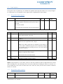
The CM1K integrated circuit uses the following patents:
Descriptions
Improved neuron circuit architecture
Circuit for pre charging a free neuron circuit
Daisy-Chain circuit for serial connection of neuron circuits
Circuit for searching/sorting data in neural networks
US patent number
US5717832
US5701397
US5710869
US5740326
Issued date
02-10-1998
12-23,-1997
01-20-1998
04-14-1998
Limitation of Liability
CogniMem Technologies, Inc. (CTI) assumes no liability whatsoever and disclaims any express, implied or statutory
warranty relating to the product described in this manual and accompanying materials (“Product”) including, but
not limited to, the implied warranty of merchantability, fitness for a particular purpose, or non-infringement. In no
event shall CTI be liable for any direct, indirect, consequential, punitive, special or incidental damages (including,
without limitation, damages for loss of profits, business interruption, or loss of information) arising out of the use
or inability to use the Product, even if CTI has been advised of the possibility of such damages. CTI makes no
representations or warranties with respect to the accuracy or completeness of the contents of this document and
reserves the right to make changes to specifications and product descriptions at any time without notice.
This Product is not designed, manufactured or intended by CTI for incorporation into products intended for use or
resale in equipment in hazardous, dangerous to life or potentially life-threatening environments, such as in the
operation of nuclear facilities, aircraft navigation or communication systems or direct life support machines, in
which the failure of products could lead directly to death, personal injury or severe physical or environmental
damage (“High Risk Activities”). The inclusion of the Product as critical component in High-Risk Activities implies
that the manufacturer assumes all risk of such use and in doing so agrees to fully indemnify CTI for any damages
resulting from such application.
Trademarks and Copyrights
This manual is copyrighted and published by CogniMem Technologies, Inc. All rights reserved. No parts of this
work may be reproduced in any form or by any means - graphic, electronic, or mechanical, including photocopying,
recording, taping, or information storage and retrieval systems - without the written permission of the publisher.
Products that are referred to in this document may be either trademarks and/or registered trademarks of the
respective owners. The publisher and the author make no claim to these trademarks.
Contact Information
www.cognimem.com
CM1K Hardware User’s Manual
2
1
1
2
3
4
5
6
Table of Contents
Table of Contents...................................................................................................................................................3
Architecture of the CM1K ......................................................................................................................................6
2.1
Top Control logic ..........................................................................................................................................6
2.2
Cluster of Neurons .......................................................................................................................................7
2.3
Recognition stage (optional usage) ..............................................................................................................7
2.4
I2C slave controller (optional usage)............................................................................................................7
The neural network ...............................................................................................................................................8
3.1
A chain of identical neurons.........................................................................................................................8
3.1.1 Parallel access to the neurons .................................................................................................................8
3.1.2 Sequential access to the neurons ............................................................................................................8
3.2
The neuron parallel bus ...............................................................................................................................9
3.2.1 Command and control lines.....................................................................................................................9
3.2.2 Timings.....................................................................................................................................................9
3.3
The control registers ..................................................................................................................................11
3.3.1 Operation modes: Normal versus Save and Restore .............................................................................11
3.3.2 Register descriptions .............................................................................................................................11
3.3.3 Neuron behavior per instruction ...........................................................................................................15
3.3.4 Commands changing the RTL neuron in chain.......................................................................................16
3.4
Test Registers .............................................................................................................................................17
3.4.1 Description.............................................................................................................................................17
3.4.2 Usage .....................................................................................................................................................17
3.5
Programming sequences............................................................................................................................18
3.5.1 Vector broadcasting...............................................................................................................................18
3.5.2 Learn a vector ........................................................................................................................................19
3.5.3 Recognize a vector .................................................................................................................................21
3.5.4 Reading the number of committed neurons .........................................................................................24
3.5.5 Reading the contents of the neurons ....................................................................................................25
3.5.6 Reading the contents of a single specific neuron ..................................................................................26
3.5.7 Loading the contents of the neurons.....................................................................................................27
3.5.8 Typical operation latency.......................................................................................................................28
The optional recognition stage ............................................................................................................................29
4.1
Control registers.........................................................................................................................................30
4.1.1 Recognition Status Register ...................................................................................................................30
4.1.2 Recognition output registers .................................................................................................................30
4.1.3 Video input registers..............................................................................................................................31
4.2
Programming sequences............................................................................................................................32
4.2.1 Size the region of interest ......................................................................................................................32
4.2.2 Move the region of interest ...................................................................................................................32
4.2.3 Recognize the region of interest............................................................................................................32
4.3
Timing constraints ......................................................................................................................................33
The optional I2C slave controller .........................................................................................................................34
5.1
Write sequence ..........................................................................................................................................34
5.2
Read sequence ...........................................................................................................................................35
5.3
Summary and Timing constraints...............................................................................................................35
5.4
I2C transmission codes...............................................................................................................................36
5.4.1 Bus Idle State .........................................................................................................................................36
5.4.2 Start Bit ..................................................................................................................................................36
5.4.3 Stop Bit...................................................................................................................................................36
5.4.4 Acknowledge Bit ....................................................................................................................................36
5.4.5 No-Acknowledge Bit ..............................................................................................................................36
CM1K buses and control lines..............................................................................................................................37
6.1
Clocks, power-up and reset........................................................................................................................38
CM1K Hardware User’s Manual
3
6.1.1 G_Reset, global reset .............................................................................................................................38
6.1.2 G_CLK, system clock ..............................................................................................................................38
6.1.3 CS_, power saving control line...............................................................................................................38
6.2
Neural network BiDir lines (parallel bus) ...................................................................................................38
6.2.1 DS ...........................................................................................................................................................39
6.2.2 RW_ .......................................................................................................................................................39
6.2.3 REG[4:0] .................................................................................................................................................39
6.2.4 DATA[15:0].............................................................................................................................................39
6.2.5 ID_..........................................................................................................................................................39
6.2.6 UNC_ ......................................................................................................................................................39
6.3
Neural network input lines.........................................................................................................................40
6.3.1 S_CHIP....................................................................................................................................................40
6.3.2 DCI..........................................................................................................................................................40
6.4
Neural network output lines ......................................................................................................................40
6.4.1 DCO ........................................................................................................................................................40
6.4.2 RDY.........................................................................................................................................................40
6.5
Digital Input Bus .........................................................................................................................................41
6.5.1 RECO_EN ................................................................................................................................................41
6.5.2 VI_EN .....................................................................................................................................................41
6.5.3 V_Clk, sensor Clock ................................................................................................................................41
6.5.4 V_FV .......................................................................................................................................................41
6.5.5 V_LV .......................................................................................................................................................41
6.5.6 V_DATA ..................................................................................................................................................42
6.6
Recognition stage output lines...................................................................................................................42
6.6.1 B_BSY .....................................................................................................................................................42
6.6.2 DIST_VAL ................................................................................................................................................42
6.6.3 CAT_VAL.................................................................................................................................................42
6.7
I2C serial bus ..............................................................................................................................................42
6.7.1 I2C_EN....................................................................................................................................................42
6.7.2 I2C_CLK ..................................................................................................................................................42
6.7.3 I2C_DATA ...............................................................................................................................................42
7
Timing considerations..........................................................................................................................................43
7.1
Registers Access Latency ............................................................................................................................43
7.1.1 Commands executing in multiple cycles (LCOMP, CAT and DIST) .........................................................43
7.1.2 Multiple read/write to the COMP register ............................................................................................44
7.2
Typical Timings Constraints........................................................................................................................44
7.2.1 Learn a vector ........................................................................................................................................44
7.2.2 Recognize a vector .................................................................................................................................45
7.2.3 Recognizing a vector received through the digital video bus ................................................................45
8
Designing hardware with CM1K ..........................................................................................................................47
8.1
Single chip configuration ............................................................................................................................47
8.1.1 Interface through the parallel bus (a) ....................................................................................................47
8.1.2 Interface through serial bus (b) .............................................................................................................47
8.1.3 CM1K configuration lines.......................................................................................................................47
8.2
Multiple chip configurations ......................................................................................................................48
8.2.1 Control through parallel bus (a).............................................................................................................48
8.2.2 Control through serial bus (b) ................................................................................................................48
8.2.3 Control through parallel bus and separate recognition stages (c) ........................................................48
8.2.4 CM1K configuration lines.......................................................................................................................49
9
Physical specifications .........................................................................................................................................50
9.1
Pinout .........................................................................................................................................................50
9.2
Mechanical specifications ..........................................................................................................................53
9.3
Electrical Specifications ..............................................................................................................................54
9.3.1 CS_, power saving control line...............................................................................................................54
9.3.2
Pull-up resistors and power saving tips ................................................................................................54
CM1K Hardware User’s Manual
4
10
FAQ .................................................................................................................................................................55
10.1
Hardware design ........................................................................................................................................55
10.2
Operation ...................................................................................................................................................55
11
Appendix A: Errata ..........................................................................................................................................56
11.1
05-11-2012, RNCOUNT limited to 16-bit value ..........................................................................................56
11.2
08-03-2011, NID incorrect if firing neurons with same distance and category .........................................56
11.3
07-03-2012, Erroneous ID_line and NSR value when more than 416 neurons committed .......................57
12
What is new in this manual ?..........................................................................................................................59
12.1.1
Revision 03-20-13 ................................................................................................................................59
12.1.2
Revision 01-09-13 ................................................................................................................................59
12.1.3
Revision 08-23-12 ................................................................................................................................59
12.1.4
Revision 08-03-2012 ............................................................................................................................59
12.2
Revision 07/03/2012 ...................................................................................................................................59
12.3
Revision from 02/17/2012 ..........................................................................................................................59
12.4
Revision from 11/1/2011 ............................................................................................................................59
12.5
Revision from 10/19/2011 ..........................................................................................................................59
12.6
Revision from 10/13/2011 ..........................................................................................................................59
CM1K Hardware User’s Manual
5
2
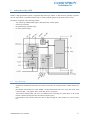
Architecture of the CM1K
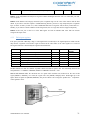
CM1K is a high-performance pattern recognition chip featuring a network of 1024 neurons operating in parallel.
Also, the chip embeds a recognition engine ready to classify a digital signal received directly from a sensor.
The CM1K is composed of the following modules
- Top control logic (NSR and RSR registers, Ready and Busy control signals)
- Clusters of 16 neurons
- Recognition stage (optional usage)
- I2C slave (optional usage)
2.1
Top Control logic
-
Synchronize communication between the clusters of neurons, the recognition state machine and the I2C
slave.
Inter-module communication is made though a bi-directional parallel bus of 25 wires: data strobe (DS),
read/write (RW_), 5-bit register (REG), 16-bit data (DATA), ready (RDY)
Inter-neuron communication also uses two additional lines indicating the global status of the neural
network: identified recognition (ID), uncertain recognition (UNC).
Communication with external control unit can be made through the same parallel bus or the serial i2C
bus.
CM1K Hardware User’s Manual
6
2.2
Cluster of Neurons
-
-
2.3
16 identical neurons operating in parallel.
All neurons have the same behavior and execute the instructions in parallel independent from the cluster
or even chip they belong to.
No controller or supervisor
Selection of one out of two classifiers: K-Nearest Neighbor (KNN) or Radial Basis Function (RBF)
Recognition time is independent of the number of neurons in use
o Recognition status in 2 clock cycles after the broadcast of the last vector component
o Distance and Category readout in 36 clock cycles per firing neuron
Automatic model generator built into the neurons
o Learn in 18 clock cycles after the broadcast of the last vector component
Save and Restore of the contents of the neurons in 258 clock cycle per neuron
Simple Register Transfer Level instruction set through of 15 registers
Most operations execute in 1 clock cycle except for Write LCOMP, Write CAT, Read CAT and Read DIST
which can take up to 19 clock cycles.
Daisy-chain connectivity between the neurons of multiple CM1K chips to build networks with thousands
of neurons .
Recognition stage (optional usage)
-
2.4
Enabled physically with RECO_EN pin and activated programmatically via a control command
Vectors received through the digital input bus are continuously recognized and the response can be
snooped directly from control lines or is readable through registers.
Recognition is made in 37 clock cycles from the receipt of the last component of a vector.
If the input signal is a video signal, the vector is extracted by the recognition stage from a user-defined
region of interest.
I2C slave controller (optional usage)
-
Enabled physically with I2C_EN pin
Receives the serial signal on the I2C_CLK and I2C-DATA lines and converts it into a combination of DS,
RW_, REG and DATA signals compatible with the parallel neuron bus.
CM1K Hardware User’s Manual
7
3
The neural network
The CogniMem chip is a fully parallel silicon neural network: it is a chain of identical elements (i.e. neurons) addressed
in parallel which have their own “genetic” material to learn and recall patterns without running a single line of
code and without reporting to any supervising unit. In addition, the neurons fully collaborate with each other
though a bi-directional and parallel neuron bus which is the key to accuracy, adaptability and speed performance. E a c h neuron incorporates information from all the other neurons into its own learning logic and
into its response logic.
The neurons can learn and recognize input vectors autonomously and in parallel. If several neurons recognize a
pattern (i.e. “fire”), their responses can be retrieved automatically in increasing order of distance (equivalent to a
decreasing order of confidence). The information which can be read from a firing neuron includes its distance,
category and neuron identifier. If the response of several or all firing neurons is polled, this data can be
consolidated to make a more sophisticated decision weighing the cost of uncertainty or else. Note that if a “bestmatch” response is sufficient for an application, the CM1K chip comes with a recognition stage which is optimized
to return this limited response 38 clock cycles after the receipt of a vector on the digital input bus of the chip.
This paragraph gives a brief overview of the neural network functionality. For a detailed description of the
neuron’s behavior and their interactions, please refer to the manual CogniMem Reference Guide.
3.1
A chain of identical neurons
A neuron can have three states in the chain: IDLE, Ready-To-Learn (RTL) or COMMITTED. It becomes committed as
soon as it learns a pattern and its category register is written with a value different from 0. Its Daisy-Chain-Out (DCO)
control line automatically rises, changing its status from Ready-To-Learn to Committed. The next neuron in the
chain becomes the Ready-To-Learn. It has its Daisy-Chain-In (DCI) high and Daisy-Chain-Out (DCO) low.
The transfer of the DCI-DCO from one neuron to the next is activated the same way whether the two consecutive
neurons belong to a same cluster or not, and even belong to a same chip or not.
3.1.1 Parallel access to the neurons
All the neurons decode and execute the commands received through the neuron bus in parallel. This bus also
allows all the firing neurons to interact with one another such that the “winner takes all” in the case of a
recognition and such that only novelty commits a new neuron in the case of learning. This is a key enabler of the
CM1K chip to deliver a recognition time independent of the number of committed neurons in the chain.
3.1.2 Sequential access to the neurons
The CM1K has the ability to save and restore the contents of its committed neurons, which is a representation of
the knowledge they have built autonomously by learning examples. In order to read the knowledge stored in the
neurons or load a knowledge file to the neurons, a special operation mode called Save and Restore allows
accessing the neurons sequentially in the chain.
CM1K Hardware User’s Manual
8
3.2
The neuron parallel bus
The neurons receive and execute instructions simultaneously through a bi-directional parallel bus composed of 26
lines:
3.2.1 Command and control lines
DS
RW_
REG
DATA
RDY
ID_
UNC_
Data strobe line
Read/Write line (default is Read with RW_=1)
5 bit register address
16-bit register data
Ready control line mixing the RDY output signal of all the neurons in the chain and indicating that the
neurons are all ready to execute a new command
Control line mixing the ID_ output signal of all the neurons in the chain and indicating that neurons
have identified the last vector and that these neurons are all in agreement for its classification.
Control line mixing the UNC_ output signal of all the neurons in the chain and indicating that neurons
have identified the last vector but that these neurons are in disagreement with its classification. This
line is an in/out line because used as an input during the execution of certain Write register.
The neurons sample a new command on the positive edge of the system clock and pull down their RDY line for the
duration of its execution. Upon completion, the RDY line is pulled back up on the positive edge of the system clock.
A Write command (DS, RW_=0, REG, DATA) must be stable on the positive edge of the system clock and released
before the next positive edge of the system clock.
A Read command (DS, RW_=1, REG) must be stable on the positive edge of the system clock and released before
the next positive edge of the system clock. DATA is stable when the RDY control line is pulled high.
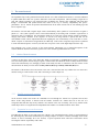
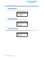
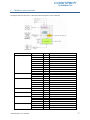
3.2.2 Timings
Depending on the REG address and also the status of the neurons on the chain, the Read and Write commands can
take between 1 and 19 clock cycles.
Write in one cycle
(REG 0x06 is the MINIF register)
CM1K Hardware User’s Manual
Read in one clock cycle
(REG 0x04 is the CAT register, read in this case in SR
mode)
9
Write in two cycles
(REG 0x02 is the LCOMP register)
Remark: When the DS signal is asserted the DATA bus must be the input value (i.e. 0x000b). It then is switched to a
tri-state mode (i.e. 0xFFFF). During the second and last cycle of the Write LCOMP the firing neurons output their
category value and DATA represents their resulting bit-per-bit AND combination (i.e. 0x0001). If this value is
different from the category of one of the firing neurons, the UNC_L line is pulled down (not the case illustrated in
the above diagram)
Read in sixteen cycles
(REG 0x03 is the DIST register)
CM1K Hardware User’s Manual
10
3.3
The control registers
3.3.1 Operation modes: Normal versus Save and Restore
The Save-and-Restore (SR) mode is used to save and restore the contents of the neurons in the least amount of
time. This feature is essential to transfer knowledge bases between hardware platforms, but also make backup
prior to training on additional examples.
Under the SR mode, the neurons become dummy memories limited to the execution of read register and write
register functions taking one system cycle each. The automatic model generator and search and sort algorithm are
disabled. The SR mode is set in bit 4 of the NSR register.
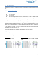
3.3.2 Register descriptions
The following table describes the 15 registers controlling the entire behavior of the neurons. For a detailed
description of the neuron’s behavior and their interactions, please refer to the manual CogniMem Technology
Reference Guide.
Description
NSR
Network Status Register
Addr
8-bit
0x0D
Normal
mode
RW
0x0B
RW
SR
mode
W
Data 16-bit/
Default
0x0000
Bit[1:0], reserved
Bit[2], UNC (Uncertain, read-only)
Bit[3], ID status (Identified, read-only)
Bit[4], SR status (default=normal)
Bit[5], KNN classifier (default=RBF)
The ID and UNC bits are updated internally after
each Write Last Comp command. ID is high if all
firing neurons report the same category. UNC is
high if several neurons fire but disagree with the
category.
KNN is a recognition mode and should not be
active while learning (since any pattern would be
recognized whatever its distance from a neuron,
the learning would create a single neuron)
*see Erratum and work around at the end of this
manual.
GCR
Global Control Register
0x0001
Bit [6:0]= Global Context Register
Bit[7]= Norm , 0 for L1, 1 for Lsup
MINIF
Minimum Influence Field
0x06
RW
MAXIF
Maximum Influence Field
0x07
RW
CM1K Hardware User’s Manual
RW
0x0002
0x4000
11
Description
NCR
Neuron Context Register
Addr
8-bit
0x00
Normal
mode
SR
mode
RW
Data 16-bit/
Default
0x0001
0x01
W
RW
0x0000
0x02
W
In normal mode
Bit[15:8]=0x00
Bit[7:0] = neuron identifier bit [23:16]
In SR mode:
Bit[15:8] = neuron identifier bit [23:16]
Bit[7]= neuron Norm , 0 for L1, 1 for Lsup
Bit [6:0]= Context value between 0 and 127
COMP
Component
Bit[15:8] = unused
Bit[7:0]= byte component of the vector to learn
or recognize. The component index can range
between 0 to 255 and is incremented
automatically after each Read or Write. It is reset
after a Write LCOMP (see next register)
If the neuron is committed and its NCR=GCR:
Update the distance register using the new
distance between the component value and the
neuron’s memory value with same index (the
norm is defined by bit 7 of the GCR). If the
component index is zero, the distance register is
reset prior to being updated.
If the neuron is the Ready-To-Learn:
Write the component value to the neuron’s
memory value with same index.
LCOMP
Last Component
0x0000
Bit[15:8] = unused
Bit[7:0]= last byte component of the vector to
learn or recognize. The component index can
range between 0 to 255 and is reset after
execution of this command.
If the neuron is committed and its NCR=GCR:
At the last cycle of this operation, the ID_ and
UNC_ lines and NSR register are updated to
report the recognition status of the vector.
Furthermore, if the status is identified (ID_ line is
low), the “identified category” is available on the
DATA bus.
CM1K Hardware User’s Manual
12
Description
INDEXCOMP
Component index
Set the memory index to an input value which
can range between 0 and 255.
Addr
8-bit
0x03
Normal
mode
W
SR
mode
W
Data 16-bit/
Default
0x0000
0x03
R
R
0xFFFF
RW
RW
0xFFFF
Note that this command does not reset the
distance register.
DIST
Distance register.
This register is updated by the neuron.
Can range between 0 and 65535 (0xFFFF)
A distance 0 means that the vector matches
exactly the model of a firing neuron. The higher
the distance, the farther the vector from the
model.
A distance of 0xFFFF means that no neuron
recognizes the last input vector.
Must be read after writing CM_LCOMP and
before reading CM_CAT
CAT
Category register
0x04
Bit 15 is read-only and reserved to indicate if the
neuron is degenerated or not
Bits [14:0] represent the category value assigned
to the pattern learned by the neuron. This value
can range between 0 and 32766 (0x7FFE)
Remark about Write CAT
- Writing a category of 0 does not commit
a new neuron, but may force existing
committed neurons to reduce their
influence fields.
Remark about Read CAT
- Reading a category of 0xFFFF means that
no neuron is firing and that the last
broadcasted vector is a novelty.
- If category is greater than 32768, it
indicates that the neuron recognizes the
last broadcasted
vector, but is
degenerated (bit15=1) so its response
might be considered with caution. The
value must be masked with 0x7FFF to
report the original value learned by the
neuron.
Must be read after the DIST register except if the
ID_ line is low and the NID register does not need
to be read after the CAT register.
CM1K Hardware User’s Manual
13
Description
AIF
Active Influence Field
In normal mode, this register is updated by the
learning logic of the neuron.
NID
Neuron Identifier
This register can be read after the category
register.
Addr
8-bit
0x05
Normal
mode
SR
mode
RW
Data 16-bit/
Default
0x4000
0x0A
R
R
0x0000*
*bit[23:16] of the neuron identifier are stored in
the unused upper byte of the NCR register.
It is the subject of an Erratum at the end of this
manual.
POWERSAVE
Dummy register
0x0E
This register can be written to ensure that the
DATA lines are in tri-state and do not draw
current from the pull-up resistors.
W
n/a
FORGET
Clear the neuron’s category register, resetting its 0x0F
status to idle. The value written to this register is
discarded.
W
n/a
Note that the neuron’s memory is not cleared,
but its index is reset to point at the first
component and this component will be
overwritten by the next Write COMP.
NCOUNT
Normal mode: Number of committed neurons. Is 0x0F
equal to 0xFFFF if all neurons of the chain are
committed.
R
R
0x0000
(see Errata)
W
n/a
SR mode: Index of the neuron pointed in the
chain. This index increments automatically after
each Read or Write CAT, and is reset to 0 after a
Write RESETCHAIN
RESET
CHAIN
Points to the first neuron of the chain. The value
written to this register is discarded.
CM1K Hardware User’s Manual
0x0C
14
3.3.3 Neuron behavior per instruction
The following table describes how the content of a neuron is updated depending on its state in the chain of
neurons. The content is divided into three types of items: memory, registers and control lines.
Memory
Component 0
Idle
Component 1
…
Component 255
Registers
Context
Minimum Influence Field
Maximum Influence Field
Ready to Learn
st
Takes the value of the 1 Write
COMP occurring after a Write
LCOMP.
The memory index is incremented
by 1 to point to the next
component.
Takes the value of the next Write
Comp or Write LCOMP.
The memory index is incremented
by 1 after a Write Comp, or is
reset to 0 after a Write LCOMP.
Committed
Can only be changed by a reset or
restore operation.
Reset the distance register
The memory index is incremented
by 1 to point to the next
component.
Can only be changed by a reset or
restore operation.
The memory index is incremented
by 1 after a Write Comp, or is reset
to 0 after a Write LCOMP.
Takes the value of the next Write
Comp or Write LCOMP. The
memory index is reset to 0.
Can only be changed by a reset or
restore operation.
Idle
Takes the value of the
Write GCR.
Takes the value of the
Write MINIF.
Takes the value of Write
MAXIF.
Ready to Learn
Takes the value of the
Write GCR.
Current value is saved if
the neuron gets
committed after a Write
CAT.
Takes the value of the
Write GCR.
Takes the value of the
Write GCR.
Distance
Category
Committed & nselect
Can only be changed by a
reset or restore
operation.
The difference between
the pointed Component
and the input value is
accumulated after each
Write Comp or Write
LCOMP.
Value is written if no
committed neuron fires
and has its own category
equal to value.
The neuron status
switches from RTL to
Committed.
Active Influence Field
CM1K Hardware User’s Manual
Inherits the smallest
distance value of the
firing neurons
15
3.3.4 Commands changing the RTL neuron in chain
Memory cell index change
Write COMP
Write LCOMP
Write INDEXCOMP
Write TESTCOMP
Write NSR
Write CAT
Read CAT
CM1K Hardware User’s Manual
Normal mode
Index + 1
Index =0
Index=k
Index=0
Save and Restore mode
Index + 1
Index=k
Index + 1
Index=0
Index=0
Index=0
16
3.4
Test Registers
The following registers are used solely for the purpose of testing the memory of all the neurons in a minimum
number of clock cycles. TESTCOMP allows filling the memory of all the neurons in a chain in 256 cycles (i.e. one per
component). TESTCAT allows committing all the neurons in a chain in one cycle.
3.4.1 Description
Description
Addr
8-bit
0x08
TESTCOMP
Test Component
Write the pointed component of all neurons
with the input value. Useful for test routines.
TESTCAT
Test Category
0x09
Write the same category to all the neurons.
Useful for test routines.
Normal
mode
n/a
SR
mode
W
Data 16-bit
/Default
0x0000
n/a
W
0x0000
Writing the value 0 to this register is equivalent
to writing the FORGET register except that it
does not reset the neuron count.
3.4.2 Usage
The Write TESTCOMP and Write TESTCAT commands are used in the test benches written to test the CM1K HDL
design.
A typical usage example is the counting of the number of neurons in a chain of CM1K
Part 1: Commit all the neurons in 2 cycles
-
Write NSR 0x10
Write TESTCAT Value
Set the SR mode
Commit all the neurons with a same category value
Part2: Read the category of the neurons until end of chain is reached
-
-
Write RESETCHAIN
Ncount=0
Do Loop
o Read CAT, cat
o Ncount++
Until cat=0xFFFF
Write NSR 0x00
CM1K Hardware User’s Manual
st
Point to the 1 neuron in chain
(Ncount-1) is the number of neurons in the chain
Cancel the SR mode
17
3.5
Programming sequences
This paragraph describes the typical programming sequences to use the neurons in standard mode and save and
restore mode.
- Broadcast a vector to all the neurons (whether to learn or recognize it)
- Recognize the last broadcasted vector
- Learn the last broadcasted vector
- Save the content of all the neurons
- Read the content of a specific neuron
- Load the content of the neurons
3.5.1 Vector broadcasting
The memory of the neurons is 256 bytes long so the vectors to learn or recognize can be composed of up to 256
components of 8-bit value.
1) Write Context (optional)
If the new vector must be associated to a context different than the current value of the Global Context or
if the distance norm coded in bit 7 of the context must be changed
2) Up to 255 Write Component
Write all the components of the input vector but the last one in the Ready-To-Learn.
For all the committed neurons with a context equal to the Global Context, their distance register is
updated after each Write Component according to the Norm in use.
3) 1 Write Last Component
For all the committed neurons with a context value equal to the Global Context register, their distance
register is updated and represents the distance between the input vector and the prototype stored in
CM1K Hardware User’s Manual
18
their memory. If the distance of a neuron is less than its influence field, the neuron “fires” meaning that it
is ready to respond to further inquiries such as a Read DIST or Read CAT commands.
Also at the end of the Write Last Component, the entire neural network has been able to evaluate if the
vector is recognized or not, and with uncertainty or not. Recognition exists is at least one neuron fires.
Uncertainty exists if at least two of the firing neurons have a different category register.
3.5.2 Learn a vector
All the neurons have their internal learning logic and teaching a vector is as simple as broadcasting its components
and then writing its category value. Optionally, the PowerSave register can be written to set the data lines in tristate mode so they do not draw current.
If this combined information (vector and category) represents novelty to the existing neurons, the Ready-To-Learn
neuron becomes committed. It stores the instructed category in its category register. Its influence field is set to
the smallest distance register of the committed neurons belonging to the same context, or the Minimum Influence
Field whichever is greater, or the Maximum influence field whichever is smaller.
The next neuron in the chain turns from idle to RTL (ready-to-learn).
If there are neurons which recognized the vector with a category other than the instructed category, they
automatically reduce their influence field to prevent such erroneous recognition in the future.
CM1K Hardware User’s Manual
19
Remark #1: If the network is full, a learning operation will have no effect. You can detect that all the neurons of
the network are already committed by executing the Read NCOUNT command which will then return the value
0xFFFF.
Remark #2: If an application requires to change learning settings such as the Minimum and Maximum Influence
Fields, this must be done prior to the broadcast of the vector to learn.
Remark #3: If the AIF of a neuron reaches the Minimum Influence Field, the bit 15 of its category register is set to
1. The neuron is said “degenerated”. It still reacts to input patterns as any other committed neuron but the bit 15
of its category indicates that the neuron was prevented from shrinking its AIF to a smaller value during training and
its response should be weighted differently than the response of another firing neuron which is not degenerated.
Example
Let’s take the example of an input vector equal to a series going from 00 to 99. This vector has a length of 100
th
components. Its first 99 components are written in sequence to the CM_COMP register and its last and 100
component is written to the CM_LCOMP register.
Broadcast the vector, learn as category 33 and read the number of committed neurons.
Sequence
For (i = 0; i<99, i++) Write CM_COMP, Vector(i);
Write CM_LCOMP, Vector(99)
Write CM_CAT, 33
Read CM_NCOUNT, ncount
Ncount will not be incremented if a committed neuron with a category register equal to 33 already recognizes
Vector. Note that this does not mean that the content of the neurons has not changed. Indeed, no new neuron has
been committed but existing committed neurons may have reduced their influence fields.
CM1K Hardware User’s Manual
20
3.5.3 Recognize a vector
A vector broadcasted to the neuron bus is evaluated by all the committed neurons in parallel. The CogniMem
network can exercise two types of classifiers: Radial Basis Function Network (RBF) or K_Nearest Neighbor classifier
(KNN). The KNN classifier always returns a response, when the RBF classifier discriminates case of positive
identification, uncertainty and unknown.
KNN
The KNN classifier discards the relationship between
the distance and influence field of a neuron. As a
consequence, all the neurons fire and their distance
and category can be read in sequence per increasing
order of distance.
RBF
The RBF classifier uses the Influence Field of the neurons
at the time of the recognition. A neuron fires only if the
distance calculated between the input vector and its
vector in memory is less than its influence field.
Since a pattern is always recognized whatever its
distance from a neuron, the KNN must not be active
during learning or it will just create a first and single
neuron.
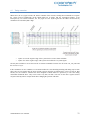
In either cases, the response of the neurons can be accessed by a succession of (Read DIST, followed by Read CAT
and optionally Read NID registers). The first distance quantifies the difference between the input vector and the
neuron with the closest pattern. The category of this neuron is the category with the highest confidence level. The
second distance quantifies the difference between the input vector and the neuron with the second closest
pattern. The category of this neuron is the category with the second highest confidence level, and so on. In the
case of the RBF classifier, all the firing neurons have been read when Read DIST returns the value 0xFFFF.
The following diagram illustrates the three levels of response which can be delivered by the neurons through the
readout of the registers NSR, DIST, CAT and NID. They are listed per increasing number of system cycles:
- Conformity, or status of the recognition (identified, uncertain or unknown)
- Best match in distance and its associated category
- All possible matches listed per increasing distance values.
CM1K Hardware User’s Manual
21
3.5.3.1 Response level 1: Classification status
As soon as the last component of a vector is broadcasted to the neurons, the ID and UNC lines are updated as well
as bit 2 and 3 of the Network Status Register (NSR).
ID =0 and UNC=0
NSR[3:0] = 0
Unknown classification
no neuron recognizes the input vector and has fired
ID=1
NSR[3:0]=8
Identified classification
one or several neurons recognize the vector and agree with its category value
UNC=1
NSR[3:0]=4
Uncertain classification
one or several neurons recognize the vector but disagree with its category value.
3.5.3.2 Response level 2: Best-match
The first Read DIST command occurring after a Write Last Component returns the distance register of the neuron
with the smallest distance, equivalent to the best match. If this distance is equal to 0, this is an exact match.
If ID=1, the category of the neuron is the only recognized category. This value is obtained with a Read CAT
command.
If UNC=1, other neurons have recognized the broadcasted vector. They may have a distance register equal or
greater than the first firing neuron, but they surely do not have the same category value. Depending on the cost of
the mistake of the application, a Response level 3 might be useful.
Remark: If the category value is greater than 0x8000 or 32768 (bit 15=1) you have a warning that the neuron is
“degenerated”. The real category value can be obtained by masking bit 15 with 0 (AND with 0x7FFF). The
degenerated flag simply indicates that the neuron was prevented from shrinking its AIF to a smaller value during
training and that its response should be weighted with care, or simply differently than the response of a neuron
which is not degenerated. For example you might want to proceed reading a response of the next firing neurons to
reinforce the positive identification of the input pattern.
3.5.3.3 Response level 3: Multiple matches
Examining the distance and category of all the firing neurons can be of interest to reinforce the accuracy of a
decision. This is done by reading consecutively the DIST and CAT registers. Each of these sequences retrieves the
response of the next firing neuron in a list ordered per increasing distance value (equivalent to decreasing
confidence levels).
If two neurons fire with the same distance but different category, their individual response are read as follows:
Read Dist, Read Cat, Read Dist, Read Cat. The second Read Dist returns the same value as the first Read Dist but is
necessary to access the category register of the second neuron.
If two neurons fire with the same distance and same category, only the response of the first one is read. The first
Read Dist will notify both neurons to stay in query, but both will output their category at the following Read Cat
CM1K Hardware User’s Manual
22
and therefore exclude themselves from the next query. A second Read Dist will return the next higher distance
value if applicable.
Remark 1: Reading the identifier of the neuron is optional. This feature can be useful to review the content of the
neuron(s) which recognize the vector.
Remark 2: In the event that two or more neurons fire with a same distance and a same category, they will all
output their identical category at the same time upon execution the Read Cat command. This means that only the
lowest identifier of these neurons will be retrieved.
Remark 3: A Write Category command can be executed immediately after a Read Distance + Read Category
sequence without having to re-enter the vector. This can be useful for applications such as in predictive
maintenance or target tracking where you want to know what is recognized prior to learning a novelty.
Remark 4: If the category value is greater than 0x8000 or 32768 (bit 15=1) you have a warning that the neuron is
“degenerated”. The real category value can be obtained by masking bit 15 with 0 (AND with 0x7FFF). The
degenerated flag simply indicates that the neuron was prevented from shrinking its AIF to a smaller value during
training and that its response should be weighted with care, or simply differently than the response of a neuron
which is not degenerated.
Rules have to be established on a “per application” basis depending on the cost of a mistake, the requirements for
a minimum throughput, minimum false negative, etc.
Example 1
Let’s take the example of an input vector equal to a series going from 00 to 99. This vector has a length of 100
th
components. Its first 99 components are written in sequence to the CM_COMP register and its last and 100
component is written to the CM_LCOMP register.
Recognition consists of broadcasting the vector and reading successively the distance and category registers of the
neurons until their response is equal to xFFFF meaning that all firing neurons have reported their results.
Sequence
For (i = 0; i<99, i++) Write CM_COMP, Vector(i);
Write CM_LCOMP, Vector(99)
st
Read response of 1 neuron:
Read CM_DIST, dist1
Read CM_CAT, cat1
nd
Read response of 2 neuron:
Read CM_DIST, dist2
Read CM_CAT, cat2
Example 2
Let’s take the example of a recognition where a vector is recognized by the firing neurons:
Distance
Category
5
8
6
8
9
7
10
7
11
7
15
7
39
5
The best match is a reference pattern of category 8 recognized with a distance 5. However if we look at the
response of all the firing neurons from a statistical stand point we can observe that the first two closest neurons
report a category 8 , but the next four firing neurons report a category 7 with a distance which is not that much
st
bigger. If the cost of an inaccurate recognition is low, the response of the 1 neuron with category 8 is the simplest
to retrieve (and very fast). On the contrary, if the application cannot afford a false-positive, it might be wiser to
involve some statistics and assume that category 7 is the dominant category and should be the one selected for a
CM1K Hardware User’s Manual
23
final decision. More sophisticated rules can be deployed including the analysis of the histogram of the categories,
and more. Some applications might even consider the generation of a “response” vector composed of all the
“firing” categories (i.e. 8,8,7,7,7,7,3,5) and to be classified by another set of neurons taught to classify the
“response” vectors. CogniMem can handle up to 127 subsets of neurons trained for different purposes. These
subsets are called Contexts.
3.5.3.4 Recognition clock cycles
(Level 1)
Conformity detection
Read NSR (1 cycle)
(Level 2)
Best match
Read Dist (18 cycles)
Read Cat (19 cycles)
Read Nid (1 cycle, optional)
37 clock cycles
1 clock cycles
(Level 3)
Detailed matches
Loop N
Read Dist (18 cycles)
Read Cat (19 cycles)
N*37 clock cycles
3.5.4 Reading the number of committed neurons
The NCOUNT register returns the number of committed neurons in the chain, EXCEPT when the chain is full
meaning that all the neurons are committed, in which case CM_NCOUNT=0xFFFF.
If N, the number of CM1K chips daisy-chained in the system is known, the readout of CM_NCOUNT=0xFFFF
becomes a simple indication that the number of committed neurons is actually N*1024.
If N is unknown, due to a reconfigurable and/or stackable hardware architecture, the readout of NCOUNT=0xFFFF
can trigger the following sequence of operations in order to obtain the number of committed neurons: Switch the
network to Save and Restore mode, point at the first neuron of the chain and start iterations reading the neurons’
category sequentially until a category 0 or 0xFFFF is reached. The number of iterations is equal to the number of
committed neurons. Calling this function might take a few seconds if your platform includes thousands of neurons.
Sequence
Write CM_NSR, 16
Write CM_RESETCHAIN, 0
CommittedNeurons =0;
Do
Read CM_CAT, Cat
If (Cat!=0) CommittedNeurons++;
While (Cat!=0)
Write CM_NSR, 0
Return(CommittedNeurons)
CM1K Hardware User’s Manual
24
3.5.5 Reading the contents of the neurons
Reading the contents of the neurons is made in the following order:
-
-
The first operation consists of setting the CM1K chip in Save_and_Restore mode and pointing to the first
neuron of the chain.
For each neuron, you can read its components, context, minimum influence field and active influence field
in any order. The category register must be read last because the instruction automatically points to the
next neuron in the chain.
Finally, when all committed neurons have been read, the last operation consists of setting the CM1K chip
back to the normal mode.
Remark 1: Note that in Save_and_Restore mode the
last component is written to the CM_COMP register and
not to the CM_LCOMP register.
Remark 2: If it is known that all neurons hold a pattern
with only M significant components with M<256, the
number of Read COMP can be limited to M, thus
speeding the Save operation.
Remark 3: If an application does not use the notion of
context, saving the context register might not be
necessary, saving one clock cycle per saved neuron.
Remark 4: Saving the MINIF is necessary if it is known
that additional training will be done at a later time to
complete or expand the knowledge.
Remark 5: You can proceed two ways to detect that all
committed neurons have been read and stop the
iterations: (1) read the CM_NCOUNT register prior to
turning the Save_and_Restore mode and set the
number of iterations to this value; (2) Iterate until you
read a category 0 which indicates that you are pointing
at the ready-to-learn neuron of the chain and that the
last committed neuron was the previous one.
CM1K Hardware User’s Manual
25
Example
Let’s take the example of a knowledge composed of neurons with 100 components each.
Sequence
Write CM_NSR, 16
Write CM_RESETCHAIN, 0
Read CM_NCOUNT, Ncount
For (i=0; i<Ncount; i++)
{
Read CM_NCR, context
For (i = 0; i<100, i++) Read CM_COMP,
Vector1(i);
Read CM_AIF, aif
Read CM_MINIF, minif
Read CM_CAT, cat
}
3.5.6 Reading the contents of a single specific neuron
Reading the contents of a specific neuron is made in the following order:
-
-
The first operation consists of setting the CM1K chip in Save_and_Restore mode and pointing to the first
neuron of the chain
th
In order to point to the i neuron in the chain, (i-1) consecutives Read CM_CAT are necessary
th
You can then read the i neuron’s components, context, minimum influence field and active influence
field in any order. The category register must be read last because the instruction automatically points to
the next neuron in the chain.
Finally, the last operation consists of setting the CM1K chip back to the normal mode.
Let’s take the example of the neuron #Index
Sequence
Write CM_NSR, 16
Write CM_RESETCHAIN, 0
For (i=0; i<Index-1; i++) Read CM_CAT, cat
Read CM_NCR, context
For (i = 0; i<100, i++) Read CM_COMP, Vector1(i);
Read CM_AIF, aif
Read CM_CAT, cat
Write CM_NSR, 0
CM1K Hardware User’s Manual
26
3.5.7 Loading the contents of the neurons
Loading knowledge to the neurons is accomplished in the following
order:
-
-
The first operation consists of clearing the existing neurons, setting the CM1K chip in Save_and_Restore
mode and pointing to the first neuron of the chain.
For each neuron, you can write its components, context, minimum influence field and active influence
field in any order. The category register must be written last since the instruction automatically points to
the next neuron in the chain.
Finally, when the neurons have been loaded, the last operation consists of setting the CM1K chip back to
its normal operation mode.
Remark 1: Note that in Save_and_Restore mode the
last component is written to the CM_COMP register and
not to the CM_LCOMP register.
Remark 2: If it is known that the patterns have a length
M with M<256, the number of Write COMP can be
limited to M, thus speeding the restore operation.
Remark 3: If you intend to use the newly committed
neurons as a KNN classifier (as opposed to the default
RBF classifier), writing the AIF register is not necessary
since it will not be used by the KNN classifier.
Remark 4: Loading the MINIF is necessary if it is known
that additional training will be done at a later time to
complete or expand the knowledge.
Remark 5: There are few cases where loading several
knowledge bases into a same chain of neurons can be
relevant. One example consists of merging neurons’
contents associated to different contexts and thus
trained independently. If you are very cautious and
clearly understand the consequences of appending the
content of neurons to a knowledge already residing in a
chip, you can discard the Write Forget command. In
such case the neuron pointed after the Write NSR will
be the first neuron available in the chain or the RTL
neuron.
Remark 6: If the content loaded into the neuron includes context values other than the default of 1, it is necessary
to execute a Write GCR at the end of the sequence so the newly loaded neurons can determine if they belong to
the currently active context or not.
CM1K Hardware User’s Manual
27
Example
Let’s take the example of a knowledge composed of 2 neurons with 100 components each, a same context value
equal to 2 and their respective AIF of x135 and x456 and categories of x33 and x22:
Sequence
Read CM_NSR, LastNSR
Read CM_GCR, Last GCR
Write CM_FORGET, 0
Write CM_NSR, 16
Write CM_RESETCHAIN, 0
For (i = 0; i<100, i++) Write CM_COMP, Vector1(i);
Write CM_NCR, x2
Write CM_AIF, x135
Write CM_CAT, x33
For (i = 0; i<100, i++) Write CM_COMP, Vector2(i);
Write CM_NCR, x2
Write CM_AIF, x456
Write CM_CAT, x22
Write CM_NSR, LastNSR
Write CM_GCR, LastGCR
3.5.8 Typical operation latency
Operation
Clock cycles
Broadcast a vector of Length L
Learn a vector of length L
Status of a vector of length L
Best match of a vector of length L
Get the K top match of a vector of length L
Save N neurons
Restore N neurons
L+3
L+3 + 18
L+3+1
L+3+37
L+3+N*37
4+(260)*N
4+(260)*N
CM1K Hardware User’s Manual
@27Mhz
L=256, N=1024, K=3
9.56 in microseconds
10.26
9.59
10.93
13.67
9860.74
9860.74
28
4
The optional recognition stage
The recognition stage of the CM1K is enabled through the RECO_EN pin and can be activated through bit 0 of the
Recognition Status Register (CM_RSR). In such case the recognition stage becomes master and the neurons must
not be accessed by an external master while the BUSY line is high (for more information, refer to timings
constraints in a paragraph below).
If V_EN is low, the data received on the V_DATA bus is directly accumulated in a 256-byte FIFO at each pulse of
V_CLK when V_FV is high.
If V_EN is high, the data received on the V_DATA bus is interpreted as a video signal. The V_LV input signal is then
necessary and defines the number of pixels per line of video. V_FV defines the number of lines per video frame. In
the case V_DATA is not accumulated directly to the FIFO but rather integrated spatially per blocks of pixels. The
calculated average value per block is then accumulated to the FIFO. This operation is called feature extraction and
used the 6 registers defining the region of interest and its internal blocks to average.
As soon as V_FV falls, the recognition stage broadcasts the content of the FIFO to the neurons using a series of
Write COMP and one Write LCOMP. It then reads the response of the best match using a Read DIST followed by
Read CAT. This data is latched to the RT_DIST and RT_CAT registers and the DIST_VAL and CAT_VAL lines pulse for
the duration of one G_CLK cycle.
Remark 1: If the digital input signal is not a video signal (V_EN=0), the V_FV signal must stay low for a minimum of
N + 37 cycles of G_CLK with N being the number of V_DATA sampled during V_FV high. Note that the CAT_VAL
pulse occurs one cycle after the N + 37 cycles. V_FV must be changed at the negative edge of V_CLK.
CM1K Hardware User’s Manual
29
4.1
Control registers
The registers of the recognition logic are enabled if the pin RECO_EN is high, and whether the VI_EN pin is high or
low. If RECO_EN is low, any attempt to read a register of the recognition logic returns 0xFFFF.
4.1.1 Recognition Status Register
Description
RSR
(1)
Recognition Status Register (see below)
Bit[2-5] are updated continuously on the positive edge of
the clock.
Bit{15::6] are unused
Addr
8-bit
0x1C
Access
R/W
Data 16-bit
Default
0x0000
*see Erratum and work around at the end of this manual.
Bit
0
ABBREV
RECO_ACTIVE
Description
Enable or disable the continuous recognition of the signal received
on the digital input bus of the chip.
R/W
W
default
0x0000
1
OUTPUT_EN
W
0x0000
2
UNC
Enable the output of the category to the DATA lines (only if
S_CHIP=1).
Status of the last recognition is uncertain, meaning that the firing
neurons do not recognize the same category.
R
0x0000
R
0x0000
R
0x0000
R
0x0000
Remark: The output register RTCAT correspond to the category of
the best match. Additional categories can be obtained by stopping
the recognition logic and executing successive read of the CM_DIST
and CM_CAT registers.
3
ID
Status of the last recognition is identified, meaning that all firing
neurons recognize the same category.
4
V_FV
*See Erratum at the end of this manual.
copy of V_FV signal
5
Reco_Active
high while recognition is being executed
Remark: The prerequisite to set the RECO_ACTIVE are that the pin RECO_EN must be high and that the neurons
hold a knowledge base. This knowledge can be built on the chip itself by teaching the neurons in real-time, or it
can be loaded from a file saved at an earlier time. In the latter case, RECO_ACTIVE must be turned off while the
neurons are restored.
4.1.2 Recognition output registers
RTDIST
(2)
Description
Addr 8-bit
Access
Real-time distance, or distance of top firing neuron
0x1D
R
CM1K Hardware User’s Manual
Data 16-bit
Default
0x0000
30
RTCAT
(2)
Real-time category, or category of top firing neuron
0x1E
R
0x0000
Remark 1: The CM_RTDIST and CM_RTCAT registers remains unchanged until the next rise of the DIST_VAL and
CAT_VAL pulses.
Remark 2: The distance and category returned by the recognition logic are the ones of the neuron with the best
match. If you want to read the response of additional firing neurons you need to stop temporarily the recognition
logic as follow: set RECO_ACTIVE to 0, read N additional DIST and CAT registers and set RECO_ACTIVE back to 1.
Similarly, if you want to read the identifier of the firing neuron, the reco logic must also be stopped temporarily.
Remark 3: The UNC_ line or the bit 3 of the RSR register are both an indicator that more than one neuron
recognize the input vector.
4.1.3 Video input registers
If the pin VI_EN of the CM1K chip is high, a video signal can be sent directly to the digital input bus. In this case the
chip extracts a signature vector from a region of interest in the video frame as the video signal as it is received.
The region of interest is described by the registers described below.
TOP
LEFT
WIDTH
HEIGHT
BWIDTH
BHEIGHT
ROIINIT
Description
Addr 8-bit
Access
Left corner of the ROI in pixels
Top corner of the ROI in pixels
Nominal width of the ROI in pixels
Nominal height of the ROI in pixels
Width of a primitive block in pixels
Height of a primitive block in pixels
Reset the ROI to default
0x11
0x12
0x13
0x14
0x15
0x16
0x1F
R/W
R/W
R/W
R/W
R/W
R/W
W
Data 16-bit
Default
200
120
340
220
20
20
0
The ROI nominal size must fit a number of primitive blocks less than or equal to 256. The relationship between the
four parameters is : NWIDTH= n*BWIDTH, NHEIGHT= m*BHEIGHT and n*m <=256.
BWIDTH and BHEIGHT define the maximum size of a square block such that 256 of them fit at the most in the
region [NWIDTH , NHEIGHT]. As a result, the region with a size [NWidth, NHeight] can be divided into up to 256
th
square blocks of equal size [BWIDTH, BHEIGHT]. The pixels of block #i are averaged to produce the i component
of the signature vector.
CM1K Hardware User’s Manual
31
4.2
Programming sequences
4.2.1 Size the region of interest
Size a region of interest with a size of 32 x 32 divided into internal blocks of 2 x 2
Sequence
Write CM_NWIDTH, 32
Write CM_NHEIGHT, 32
Write CM_BWIDTH, 2
Write CM_BHEIGHT, 2
4.2.2 Move the region of interest
Move the region of interest to the location (10,12) and learn it as category 33
Sequence
Write CM_LEFT, 10
Write CM_TOP, 12
Write CM_RSR, 1
Write CM_CAT, 33
4.2.3 Recognize the region of interest
As soon as bit 0 of the RSR is high, the region of interest in the next frame is recognized. The result of the
recognition is latched in the RT_DIST and RT_CAT registers until a next frame occurs.
Sequence
Write CM_RSR, 1
Read CM_RTCAT
Read CM_RTDIST
CM1K Hardware User’s Manual
32
4.3
Timing constraints
When active, the reco_logic becomes the master controller of the neurons, sending them commands to recognize
the vectors received continuously on the digital input bus. To ensure that the recognition sequence is not
interrupted by an external controller, the reco_logic rises the B_BSY signal and the CM1K will discard any
command received while B_BSY is high.
o
o
B_BSY rises on the negative edge of the system clock as soon as frame valid falls
B_BSY falls on the negative edge of the system clock when the CAT_VALID signal.
The only time available to receive and execute an external command is between the fall of the CAT_VAL pulse and
the next rise of F_FV.
If this command is an I2C command, its execution includes the serial decoding/encoding and timing may become
short. Since we can assume that the most relevant registers when the recognition stage is active are the RT_DIST
and RT_CAT, the CM1K I2C controller has been designed to handle them in a special way to waive the timing
constraints mentioned above. They can be read at any time, but this is not true for the other registers such as
CM_LEFT and CM_TOP for example which allow changing the position of the ROI.
CM1K Hardware User’s Manual
33
5
The optional I2C slave controller
The CM1K features a serial interface slave running at 100 or 400 Kbit per second. In a configuration with N CM1K
chips daisy-chained together, only one of them can enable its I2C controller. The latter will convert the commands
received though the I2C lines into commands transmitted over the parallel control bus.
The two-wire serial interface defines several different transmission codes, as follows:
- A start bit
- An eight-bit address consisting of SlaveID, a 7-bit fixed address, followed by 1 bit of direction (0 if request
to Write, 1 is request to Read). The 7-bit SlaveID of the CM1K is 0x4A. The 8-bit address is 0x94 in the case
of a Write and 0x95 in the case of a Read.
- An acknowledge bit.
- An 8-bit message (The CM1K uses 16-bit data for its internal registers, thus requiring two 8-bit transfers
per read or write command)
- A stop bit
Definition:
- SlaveID= 0x4A
- SlaveID_Wr= 0x94
- SlaveID_Rd=0x95
5.1
Write sequence
Step
1
Master
A typical write sequence begins by a master sending a
start bit followed by SlaveID_Wr
2
3
If the address is not equal to SlaveID the request
is ignored by the CM1K. Otherwise it returns an
acknowledge bit to the master.
The master then transfers the 8-bit address of the
register to write.
4
5
6
7
8
9
Slave
The slave sends an acknowledge bit to indicate
that the register address has been received.
The master transfers the lower byte of the 16-bit data
to write.
The slave sends an acknowledge bit.
The master transfers the upper byte of the 16-bit data
to write.
The slave sends an acknowledge bit.
The master stops the request by sending a stop bit.
Example: The waveform below illustrates a Write command. The value 0x0284 is written to a register 0x09 of a
device with a slave address 0xB8 (not a CM1K).
CM1K Hardware User’s Manual
34
5.2
Read sequence
Step
1
Master
A typical read sequence begins by a master sending a
start bit followed by the SlaveID_Wr.
2
3
If the address is not equal to SlaveID the request is
ignored by the CM1K. Otherwise it returns an
acknowledge bit to the master.
The master then transfers the 8-bit address of the
register to read.
4
5
6
7
8
9
Slave
The slave sends an acknowledge bit to indicate that
the register address has been received.
The master sends a start bit followed by the
SlaveID_Rd to specify that a read is about to happen
from the register.
The slave sends an acknowledge bit.
The master clocks out the lower byte of the 16-bit
data read from the register. The master sends an
acknowledge bit after the eight-bit transfer.
The master clocks out the upper byte of the 16-bit
data read from the register. The master sends an
acknowledge bit after the eight-bit transfer.
The data transfer is stopped when the master sends
a no-acknowledge bit.
Example: The waveform below illustrates a Read command. The value 0x0284 is read back from the register 0x09
of a device with a slave address 0xB8 (not a CM1K).
5.3
Summary and Timing constraints
Sequence from the master
Start sequence
Write
Write SlaveID_Wr
Write 8-bit Register value
Request
Write most significant 8-bit of the
register’s data value
Write least significant 8-bit of the
register’s data value
CM1K Hardware User’s Manual
Read
Write SlaveID_Wr
Write 8-bit Register value
Resend Start
Write SlaveID_Rd
Read most significant 8-bit of the
register’s data value
Read least significant 8-bit of the
35
Stop sequence
STOP signal
register’s data value
NACK signal
The B_BSY signal is the CM1K is pulled high during the processing of an I2C request.
Remark: If the reco_logic is running, sending an I2C request might not fit within the ~B_BSY time frame which
starts at the fall of V_FV and finishes at the rise of CAT_VAL. The RTDIST and RTCAT registers can be read at any
time over the I2C bus because their access does not require any interruption of CM1K parallel bus, but any other
command must be submitted carefully when B_BSY is low and RDY is high.
5.4
I2C transmission codes
5.4.1 Bus Idle State
The bus is idle when both the data and clock lines are HIGH. Control of the bus is initiated
with a start bit, and the bus is released with a stop bit. Only the master can generate the start and stop bits.
5.4.2 Start Bit
The start bit is defined as a HIGH-to-LOW transition of the data line while the clock line is HIGH.
5.4.3 Stop Bit
The stop bit is defined as a LOW-to-HIGH transition of the data line while the clock line is HIGH.
5.4.4 Acknowledge Bit
The master generates the acknowledge clock pulse. The transmitter (which is the master when writing, or the slave
when reading) releases the data line, and the receiver indicates
an acknowledge bit by pulling the data line low during the acknowledge clock pulse.
5.4.5 No-Acknowledge Bit
The no-acknowledge bit is generated when the data line is not pulled down by the receiver during the
acknowledge clock pulse. A no-acknowledge bit is used to terminate a read sequence.
CM1K Hardware User’s Manual
36
6
CM1K buses and control lines
This chapter describes the buses, control lines and interrupt lines of the CM1K chip.
Configuration lines
Clock and Reset
Parallel bus
Neuron output lines
I2C bus
Digital input bus
Output lines
CM1K Hardware User’s Manual
Symbol
VCC
VCCIO
GND
S_CHIP
DCI
DCO
I2C_EN
RECO_EN
V_EN
G_CLK
G_RESET_
CS_
DS
R/W_
REG[0:4]
DATA[0-15]
UNC_
ID_
RDY
I2C_SDA
I2C_SDK
V_CLK
V_FV
V_LV
V_DATA[0:7]
DIST_VAL
CAT_VAL
B_BSY
Type
Input
Output
Input
Input
Input
Input
Input
Bidir
Bidir
Bidir
Bidir
Bidir
Bidir
Bidir
Bidir
Input
Input
Input
Input
Input
Output
Output
Output
Description
Core power supply (1.2v)
IO power supply line (3.3 v)
Ground line
Single chip mode
Daisy Chain In
Daisy Chain Out
I2C enable
Recognition enable
Video enable
System clock
Hardware reset
Enable chip activity
Data strobe line
Read/Write
Register
Data
Uncertain_low line
Identified_low line
Ready line
I2C serial data line
I2C clock
Video clock
Video frame valid
Video line valid
Video data line 0
Distance valid line
Category valid line
Bus busy line
37
6.1
Clocks, power-up and reset
6.1.1 G_Reset, global reset
The CM1K is reset at power-up by pulling down the G_RESET_l pin for a minimum of 5 clock cycles. An internal
reset signal is then sustained for 255 clock cycles to filter any bouncing of the G_RESET_l external pulse. It is
propagated internally to the neurons, the recognition stage and the i2c slave controller so all registers are set to
their default values. In a multi-chip configuration, the same G_RESET_ must be connected to all chips.
6.1.2 G_CLK, system clock
The CM1K operates at a typical system clock of 27 MHz. If multiple CM1K are connected in parallel the typical
system clock is 16 Mhz.
6.1.3 CS_, power saving control line
The CS_ line controls the propagation of the system clock G_CLK to the neurons, the reco_logic and the i2c slave
controller of the chip. It is pulled low by default letting the clock run continuously.
Pulling up the the CS_ line when the CM1K is unused reduces considerably its power consumption (from 500 mW
to 25 mW). On the other hand the timings to pull CS_ back down and let the system clock pass through must be
accurate: (1) It must be pulled down on a negative edge of G_CLK when the external data strobe (DS) is pulled up
at the latest. (2) It must be released on the negative edge of the system clock following the rise of the RDY signal at
the earliest or the fall of the B_BSY signal.
6.2
Neural network BiDir lines (parallel bus)
The parallel bus is used to transmit the Read/WriteRegister commands to all the neurons at once. It is composed of
26 lines:
DS
RW_
REG
DATA
Data strobe signal
Read/Write signal
5-bit register value
16-bit data value
1
1
5
16
RDY
ID_
UNC_
Ready control signal
Identified control signal (see Erratum)
Uncertain control signal necessary to learn
1
1
1
The neurons sample these signals on the positive edge of the system clock G_CLK. Their setup time must be at
least 5 nanoseconds before the positive edge of G-Clock. The hold time must be at least 5 nanoseconds after the
positive edge of the clock. The signals have to be released before the next positive edge of the clock to ensure that
the data bus becomes bi-directional for proper execution of the commands requiring snooping of the bus.
Up to eight CM1K running at a system clock of 16Mhz can be connected to the same parallel bus without any redrive. Beyond a chain of 8 CM1K chips, buffers must be inserted.
CM1K Hardware User’s Manual
38
The control commands sent to the parallel bus can be received from two types of sources:
An external master controller
- One of the two internal master controllers residing in the CM1K chip and which comprise the recognition
stage or the I2C slave controller. This second case is only relevant in an architecture with multiple daisychained chips where one of them has its pin I2C_EN high and/or RECO_EN high. The bus lines become
bidirectional to allow the neurons of the different chips to receive the commands and mix their responses
on the bus during the learning or recognition operations.
6.2.1 DS
The data strobe line, DS, must be asserted and de-asserted at the negative edge of G_CLK. It must be asserted only
when the RDY line is high.
6.2.2
RW_
The Read/Write line, RW_, must be low to write and high to read. It is low by default. This signal is sampled on the
positive edge of G_CLK when DS is high.
6.2.3 REG[4:0]
The five Register lines, REG, represent the 5-bit address of the register to read or write. They are sampled on the
positive edge of G_CLK when DS is high.
6.2.4 DATA[15:0]
The 16 DATA lines are connected to open collectors and can have three different states:
- During a write operation (CM_RW low and DS high), DATA is the 16-bit value to write to the selected
register. It is sampled by the neurons at the positive edge of G_CLK when DS is high and RW is low.
- At the end of a read operation (RW high and RDY rising), DATA is the 16-bit value of the selected register.
It can be read on or after the rising edge of CM_RDY after the fall of DS. The default output value is
0xFFFF.
- During the execution of the commands which last more than one clock cycles, the DATA lines must be
released to allow the mixing and snooping of the responses of all the neurons connected in parallel in a
same chain. These operations are the Write LCOMP, Write CAT, Read DIST and Read CAT.
6.2.5 ID_
The Identified line, ID_, is pulled down when all the neurons recognizing the last input vector are all in agreement
and return the same category. This line is updated each time the last component of a vector is broadcasted to the
neurons either through a Write LCOMP command or through the real-time recognition logic of the CM1K. The
rd
actual update occurs at the 3 negative edge of the clock during the execution of the Write LCOMP. The ID_ line is
released at the next Write COMP.
The ID_ line is also continuously latched in bit [3] of the NSR and RSR registers of the chip at the positive edge of
the clock.
The ID_ line is erroneous in the CM1K when more than 416 neurons are committed in the chip. This impacts also
the readout of the NSR and RSR registers. Refer to the Erratum at the end of this manual for a description of the
problem and its simple work around.
6.2.6 UNC_
The Uncertain line, UNC_, line is bidirectional and shall not be driven. It is an output during a recognition operation
and an input during a learning operation.
CM1K Hardware User’s Manual
39
UNC_ is pulled down when the neurons recognizing the last input vector have different categories. This update
occurs each time a Write LCOMP is executed whether it is initiated by an external controller or by the internal
rd
recognition logic of the chip. The actual update occurs at the 3 negative edge of the clock during the execution of
the Write LCOMP. The UNC_ line is released at the next Write COMP.
The UNC_ line is also continuously latched in bit [2] of the NSR and RSR registers of the chip. at the positive edge of
the clock.
During a Write CAT, this line is asserted by the neurons if the last input vector is recognized as a novelty and must
be stored into a new neuron.
6.3
Neural network input lines
6.3.1 S_CHIP
By default the S_CHIP pin is pulled down to configure the parallel bus (DS, RW_l, REG and DATA) as bidirectional
and allow the neurons of multiple CM1K chips to receive commands synchronously and interact with one another.
If an architecture uses a single CM1K chip connected to a control unit via its I2C bus, then its parallel bus can be
disabled, thus reducing considerably the power consumption. If the reco logic of the chip is activated, it is possible
to overwrite the settings of the DATA lines through the RSR register. In that case, the RT_CAT register is latched on
the DATA lines at each CAT_VAL pulse.
6.3.2 DCI
Until the DCI line of a CM1K chip is high, its neurons are idle. As soon as the DCI line rises, the neurons of the chip
become active, meaning ready to learn and recognize.
In a configuration with multiple chips, the Daisy-Chain-In (DCI) line of the first CM1K chip must be high. For the
subsequent chips, the connection between their DCO and DCI lines allows to physically arrange them in a chain.
The DCI line of a CM1K must be connected to the DCO of the previous CM1K chip in the chain. Its status is then
controlled by the neurons of the previous chip.
6.4
Neural network output lines
6.4.1 DCO
The Daisy-Chain-Out (DCO) line of a CM1K must be connected to the DCI of the next CM1K chip in the chain, if
applicable. It is low by default and will rise when the last neuron of the chip gets committed. If this line is
connected to the DCI of another CM1K chip, the later will awake its neurons to become Ready-To-Learn.
6.4.2 RDY
The Ready line, RDY, is pulled down by the neurons during the execution of a command and released upon its
termination. It is updated at the positive edge of the system clock G_CLK whether or not the command is
recognized by the neurons.
CM1K Hardware User’s Manual
40
6.5
Digital Input Bus
The digital input bus is composed of 10 or 11 lines depending if the input signal is a video signal or not.
VCLK
V_FV
V_LV
V_DATA
Video or Vector Input Digital Clock
Video or Vector Valid control signal
Video Line Valid control signal (discard if input is not video)
Video or Vector Data
6.5.1 RECO_EN
Recognition_Enable enables the use of the V_DATA input bus and the real-time recognition engine. If several
CM1K chips are connected in parallel, only one chip can have its RECO_EN pin set to 1. In addition, if the chain of
CM1Ks shall receive its command from an external host over its I2C lines, the chip with its pin I2C_EN=1 must be
the same as the chip with its pin RECO_EN=1.
This pin is connected to an internal pull-up so it is enabled by default. For power-savings consideration, it should
be grounded if unused.
6.5.2 VI_EN
Video_Enable indicates if the digital input bus receives a video signal and if consequently the recognition engine is
in charge of generating the vector broadcasted to the neurons. If changed dynamically, the status of this pin must
be changed at the negative edge of V_CLK.
This pin is connected to an internal pull-up so it is enabled by default. For power-savings consideration, it should
be grounded if unused.
6.5.3 V_Clk, sensor Clock
Optionally, the CM1K can receive vector data directly on its digital input bus. It is then sampled at the external
clock rate V_Clk. A typical clock rate for V_Clk is 27 Mhz. A maximum clock rate of 44 Mhz has been successfully
tested.
- If the pin VI_EN=0, V_CLK is the sampling clock for the input V_DATA bus and it does not have to be a
periodic signal.
- If the pin VI_EN=1, V_CLK is the Video clock signal (up to 27 Mhz) of the sensor.
6.5.4 V_FV
Video Frame Valid or Vector Feature Valid.
If V_EN=1, V_FV stands for Frame valid and is a synchronization signal supplied by the video sensor.
If V_EN=0, V_FV stands for Feature Valid. It must be set high for the duration of the vector data input on V_DATA
bus. V_FV must stay low for a minimum of N + 37 cycles of G_CLK with N being the number of V_DATA sampled
during V_FV high. Note that the CAT_VAL pulse occurs one cycle after the N + 37 cycles. V_FV must be changed at
the negative edge of V_CLK.
6.5.5 V_LV
Video Line Valid signal of the sensor (used if VI_EN=1 only)
CM1K Hardware User’s Manual
41
6.5.6 V_DATA
Video Data or Vector Data depending on the VI_EN settings:
If VI_EN=0, this 8-bit data signal can come from a sensor or be generated by an external controller.
If VI_EN=1, this 8-bit data signal must be connected to the 8 highest bit of the video signal.
6.6
Recognition stage output lines
6.6.1 B_BSY
The Bus Busy line is asserted during the execution of an internal cycle such as a reset cycle, a recognition cycle, an
I2C read or write command received from an external controller, etc. An external master controller must verify
that B_BSY is low prior to sending a command. Otherwise the command will be discarded. This signal is updated at
the negative edge of the G_CLK.
6.6.2 DIST_VAL
The Distance Valid signal rises on the negative edge of G_CLK when the real time distance (Addr 0x01D) of the last
recognition is available on the DATA output bus. This strobe lasts one clock cycle.
6.6.3 CAT_VAL
The Category Valid signal rises on the negative edge of G_CLK when the real-time category (Addr 0x1E) of the last
recognition is available on the DATA output bus. This strobe lasts one clock cycle.
6.7
I2C serial bus
The CM1K I2C slave controller can receive commands from an external I2C master controller operating at a speed
of 100 or 400 Kbit per second. It is enabled by setting the I2C_EN pin to 1. It converts the clock and serial data
received on the I2C_SCK and I2C_SDA pins into an internal data strobe signal (DS), Read/Write signal (RW_),
register value (REG) and data value (DATA). If the STANDALONE pin is set to 0, these signals are also be
broadcasted to the bidirectional parallel bus of the chip for use by the other CM1K chips.
6.7.1 I2C_EN
I2C_EN enables the CM1K to communicate with an external I2C master controller. If several CM1K chips are
connected in parallel, only one chip can have its I2C_EN pin set to 1. In addition, if the chain of CM1Ks shall
recognize a video or other digital signal received by one of them through its digital bus, the chip with its pin
RECO_EN=1 must be the same as the chip with its pin I2C_EN=1. This pin is connected to an internal pull-up so it is
enabled by default. For power-savings consideration, it should be grounded if unused.
6.7.2 I2C_CLK
Serial Clock. Must be connected to a pull-up resistor of 4.7 KOhms.
6.7.3 I2C_DATA
Serial Data. Must be connected to a pull-up resistor of 4.7 KOhms.
CM1K Hardware User’s Manual
42
7
7.1
Timing considerations
Registers Access Latency
The following table reports the number of clock cycles (cc) necessary to read and write the registers of the CM1K
chip. The cycles are counted from the first rising edge of the system clock upon the receipt of the DS signal, to the
rising edge of the READY signal upon execution of the command.
Addr
Register
Description
0x00
0x01
0x02
NCR
COMP
LCOMP
Neuron Context Register
Component
Last Component
0x03
0x03
0x04
INDEXCOMP
DIST
CAT
Component Index
Distance
Category
0x05
0x06
0x07
0x08
0x09
0x0A
0x0B
0x0C
AIF
MINIF
MAXIF
TESTCOMP
TESTCAT
NID
GCR
RESETCHAIN
Active Influence Field
Minimum Influence Field
Maximum Influence Field
Test Component
Test Category
Neuron Identifier
Global Context Register
Learn and Recognition
mode
Write cycles
Read
cycles
1
1 if no neurons
3 otherwise
1
1 if ID, 19
otherwise
Save and Restore
mode
Write
Read
cycles
cycles
1
1
1
1
1
18
3 if ID, 19
otherwise
1
1
1
1
1
1
1
1
1
1
1
1
1
1
1
1
1
0x0D NSR
0x0F FORGET
0x0F NCOUNT
Network Status Register
Clear the neurons
Committed neurons
1
1
1
1
0x11
0x12
0x13
0x14
0x15
0x16
0x1C
0x1D
0x1E
TOP
LEFT
WIDTH
HEIGHT
BWIDTH
BHEIGHT
RSR
RTDIST
RTCAT
Left corner of the ROI
Top corner of the ROI
Width of the ROI
Height of the ROI
Width of a block
Height of a block
Recognition Status
st
Distance of 1 firing neuron
st
Category of 1 firing neuron
1
1
1
1
1
1
1
1
1
1
1
1
1
1
1
0x1F
ROIINIT
Reset the ROI to default
1
1
1
7.1.1 Commands executing in multiple cycles (LCOMP, CAT and DIST)
Accessing most registers takes a single clock cycle. In Learn and Recognition mode, reading and writing the LCOMP,
DIST and CAT registers can take between 3 and 19 clock cycles depending on the content of the neuron at the time
of the execution. This means that two neurons can execute a same instruction in different number of clock cycles
depending on its status and internal registers’ values. For example a neuron which does not recognize an input
CM1K Hardware User’s Manual
43
pattern will execute the RDIST instruction in 1 cycle, when a neuron which recognizes the pattern (i.e. fires) will
participate to the Search and Sort race for up to 16 clock cycles. The Ready line of the chip indicates when all the
neurons have finished the execution of an instruction and can receive a new one.
Write LCOMP (0x02), Read DIST (0x03), Read and Write CAT (0x04) are "snooping" commands meaning they are
making open collector bus mixing. The release of the DATA lines as well as the ID_ and UNC_ lines after the fall of
the DS signal is critical so they can snoop properly.
7.1.2 Multiple read/write to the COMP register
Broadcasting a vector to the neurons is a succession of Write COMP (up to 255 times) ended with a Write LCOMP.
The series of Write COMP can be executed with a sustained DS signal provided that the data is updated and stable
at each new positive edge of the system clock. For reference, the waveforms shown under the paragraph
“Recognizing a vector received through the digital video bus” illustrate the use of a sustained DS signal during the
feed of all but the last component value.
7.2
Typical Timings Constraints
In the example below, a vector of 8 components is learned and then recognized. The resolution of the diagrams
does not allow reading the DATA values of the components and the category, but this is not important for
understanding the timing constraints of the chip.
The DS, RW_, REG and DATA signals are updated at the negative edge of the system clock (G_CLK) so that they are
stable when the neurons read them at the next positive edge of G_CLK. The RDY signal is then immediately pulled
down by the neurons and released at the first positive edge of G_CLK following the completion of the command.
The duration during which the RDY signal is low represents the execution time of the command.
In the case of a Read command, the output DATA is ready to be read when RDY rises.
7.2.1 Learn a vector
The sequence of instructions consists of 7 Write COMP, 1 Write LCOMP, and 1 Write CAT.
When REG is equal to 01, each DS pulse triggers a Write COMP lasting one cycle of G_CLK. The RDY signal has the
same duration as the DS only shifted by one half clock cycle.
When REG is equal to 02, the DS pulse triggers a Write LCOMP. The RDY signal is pulled down for 3 cycles. The fact
that both lines ID_l and UNC_l are pulled up indicates that the input vector is not recognized by any existing
neuron. The subsequent Write CAT command will necessarily commit a new neuron.
CM1K Hardware User’s Manual
44
When REG is equal to 04, the DS pulse triggers a Write CAT. The RDY signal is pulled down for 19 cycles.
7.2.2 Recognize a vector
The sequence of instructions consists of 7 Write COMP, 1 Write LCOMP, 1 Read DIST and 1 Read CAT.
When REG is equal to 01, each DS pulse triggers a Write COMP. The RDY signal is pulled down for one cycle.
When REG is equal to 02, the DS pulse triggers a Write LCOMP. The RDY signal is pulled down for 3 cycles. The
UNC_l is pulled down at the last negative edge of G_CLK before RDY is pulled back up. This indicates that the input
vector is recognized by more than one neuron and that different categories are identified.
When REG is equal to 03 and RW_l remains high, the DS pulse triggers a Read DIST. The RDY signal is pulled down
for 18 cycles which is the duration of the Search and Sort looking for the firing neuron with the smallest distance
value. This distance is equal to 08.
When REG is equal to 04 and RW_l remains high, the DS pulse triggers a Read CAT. The RDY signal is pulled down
for 19 cycles which is the duration of the Search and Sort looking for the firing neuron with a distance register
equal to 08 and the smallest category value. This category is equal to 01.
Remark: Since it is known that the recognition status is uncertain (UNC_L is low), executing another series of Read
DIST followed by Read CAT would report the distance and category of the next neuron with the smallest distance.
7.2.3 Recognizing a vector received through the digital video bus
In the following example, RECO_EN and V_EN are both pulled up so the reco_logic of the chip can continuously
recognize the video data received through the V_CLK, V_FV, V_LV and V_DATA.
Immediately after the fall of V_FV, the B_BSY line rises indicating that the recognition stage is active and
communicating with the neurons.
The DS, RW_l, REG and DATA seen in the above diagram are generated internally by the reco_logic stage and
broadcasted to the parallel bus so the neurons of all the CM1K chips in the chain can participate to the recognition
(and not only the neurons of the CM1K with the active recognition stage).
CM1K Hardware User’s Manual
45
The first DS is sustained for four clock cycles to broadcast a vector of four components to the neurons. The REG
register is equal to 01 during the first 3 cycles to execute a Write COMP. It is then switched to the value 02 to
execute a Write LCOMP. The ID_l signal falls two clock cycles later indicating that the vector is recognized with
certainty by the firing neurons. The RDY signal falls as soon as the neurons start executing the first Write COMP
and remains low until the Write LCOMP is completed.
The second DS triggers a Read DIST. The RDY signal is pulled down for 18 cycles which is the duration of the Search
and Sort looking for the firing neuron with the smallest distance value. This distance is equal to 00 indicating an
exact match. The DIST_VAL pulse rises one clock cycle after the RDY signal to notify that DATA has been latched to
the RT_DIST register of the reco_logic.
The third DS triggers a Read CAT. The RDY signal is pulled down for 3 cycles only because a Search and Sort is not
necessary (it would extend the execution by 16 more cycles). This is no surprise since the ID_l signal has already
indicated that the input vector is recognized with certainty. The CAT_VAL pulse rises one clock cycle after the RDY
signal to notify that DATA has been latched to the RT_CAT register of the reco_logic.
CM1K Hardware User’s Manual
46
8
Designing hardware with CM1K
One of the benefits of the CM1K architecture is that you can cascade multiple chips in parallel to expand the size of
the neural network by increment of 1024 neurons. The behavior of the neurons in a single-chip or multiple-chips
configuration remains the same. The recognition logic on the other hand can only be activated on one chip of the
chain.
8.1
Single chip configuration
8.1.1 Interface through the parallel bus (a)
The CM1K can learn and recognize vector data transmitted
by the control unit through its parallel control bus (DS,
RW_, REG, DATA). If the RECO_EN pin is set to 1, vector
data can be transmitted through the digital input bus and
the response of the neuron with the best match latched to
registers. Note that if an application simply needs to
monitor the recognition status, the parallel control lines,
CAT_VAL and DIST_VAL can be sufficient outputs.
8.1.2 Interface through serial bus (b)
The CM1K can learn and recognize vector data
transmitted by the control unit through the serial
bus (I2C_CLK and I2C_DATA). If the RECO_EN pin is
set to 1, vector data can be transmitted through the
digital input bus and the response of the neuron
with the best match latched to registers. Note that if
an application simply needs to monitor the
recognition status, the parallel control lines, CAT_VAL
and DIST_VAL can be sufficient outputs.
In the case of a single chip, it is recommended to set its S_CHIP pin to 1 in order to lower its power consumption.
Indeed, the neurons of a single chip do not have to output and multiplex their data with other chips. Also, when
S_CHIP=1 and the recognition logic is active, the value of the best distance and category can be read directly on
the DATA bus when the DIST_VAL and CAT_VAL lines pulse.
8.1.3 CM1K configuration lines
S_CHIP
G_CLK
DCI
I2C_EN
RECO_EN
V_CLK, V_FV, V_DATA
V_EN
V_LV
CAT_VALID, DIST_VALID
CM1K Hardware User’s Manual
First CM1K in chain
1
Typical 27 Mhz
1
0 in config (a), 1 in config (b)
Optional
Used if RECO_EN=1
Used if RECO_EN=1
Equiv to line valid if V_EN=1, unused otherwise
Active if RECO_EN=1 and if the register RSR[1]=1
Other CM1Ks
n/a
n/a
n/a
n/a
n/a
n/a
n/a
n/a
47
8.2
Multiple chip configurations
When multiple CM1K are connected in parallel to expand the size of the neural network, their S_CHIP pin must be
set to 0. This setting turns the neuron parallel bus (DS, RW_, REG, DATA) into a bidirectional bus allowing the
neurons of different chips to automatically interact with one another when necessary.
8.2.1 Control through parallel bus (a)
A chain of CM1K can learn and recognize vector data transmitted by the control unit through the parallel control
bus (DS, RW_, REG, DATA). The control unit can also edit the network global registers and read the detailed
response of all the firing neurons if necessary.
As an option if the RECO_EN pin is set to 1, vector data can be transmitted through the digital input bus and the
response of the neuron with the best match latched to registers by the recognition stage. Note that if an
application simply needs to monitor the recognition status, the parallel control lines, CAT_VAL and DIST_VAL
output by the first chip can be sufficient outputs.
8.2.2 Control through serial bus (b)
If an application requires a low connectivity to a chain of neurons, the control unit can interface to the first CM1K
of the chain via its serial bus (i.e. 2 lines). The CM1K converts the serial data to a (DS, RW_, REG and DATA) which is
then transmitted to all the CM1K chips though the bi-directional parallel control bus.
As an option if the RECO_EN pin is set to 1, vector data can be transmitted through the digital input bus and the
response of the neuron with the best match latched to registers by the recognition stage. Note that if an
application simply needs to monitor the recognition status, the parallel control lines, CAT_VAL and DIST_VAL
output by the first chip can be sufficient outputs.
8.2.3 Control through parallel bus and separate recognition stages (c)
Multiple CM1K chips can be used to recognize different regions of interest in a same image, or to recognize a same
region but against different knowledge loaded in the CM1K chips.
CM1K Hardware User’s Manual
48
8.2.4 CM1K configuration lines
S_CHIP
DCI
I2C_EN
RECO_EN
V_CLK, V_FV, V_DATA
V_EN
V_LV
CAT_VALID, DIST_VALID
CM1K Hardware User’s Manual
First CM1K in chain
0
1
0 in config (a) and (e)
1 in config (b)
Optional in config (a) and (b)
1 in config (e)
Used if RECO_EN=1
Used if RECO_EN=1
Equiv to line valid if V_EN=1, unused otherwise
Active if RECO_EN=1 and if the register RSR[1]=1
Other CM1Ks
0
DCO of previous CM1K
in config (a) and (b)
1 in config (e)
0
0 in config (a) and (b)
1 in config (e)
n/a
n/a
n/a
n/a
49
9
9.1
Physical specifications
Pinout
12
13
14
15
16
17
18
19
20
21
22
23
24
25
76
11
77
10
78
9
79
8
80
7
81
6
82
5
83
4
84
VCCIO
G_RESET
VCC
I2C_EN
3
DATA[6]
VCCIO
DATA[7]
VCCIO
DATA[8]
DATA[9]
VCCIO
VCC
DATA[10]
VCC
VCCIO
DATA[11]
DATA[12]
VCC
GND
DATA[13]
VCC
DATA[14]
VCC
DATA[15]
CAT_VAL
B_BSY
VCC
S_CHIP
RSVD
RSVD
2
85
86
88
89
87
90
91
92
93
94
95
96
97
98
99
100
1
DATA[5]
VCCIO
DATA[4]
VCC
VCCIO
VCC
DATA[3]
VCCIO
DATA[2]
VCC
DATA[1]
VCCIO
DATA[0]
DCO
VCC
VCC
VCCIO
DIST_VAL
GND
VCC
VCC
VCCIO
DS
RDY
VCCIO
STANDBY
VCCIO
G_CLK
VCCIO
I2C_SCK
VCC
VCCIO
DCI
VCC
I2C_SDA
V_EN
VCC
V_DATA[0]
V_DATA[1]
VCC
V_DATA[2]
VCC
V_DATA[3]
V_DATA[4]
V_DATA[5]
75
74
73
72
71
70
69
68
67
66
65
64
63
62
61
60
59
58
57
56
55
54
53
52
51
ID UNC
VCCIO
R/W
RECO_EN
VCC
VCCIO
REG[4]
VCC
REG[3]
REG[2]
VCCIO
VCC
REG[1]
REG[0]
VCC
VCCIO
V_CLK
VCCIO
VCC
V_FV
VCC
V_LV
V_DATA[7]
V_DATA[6]
50
49
48
46
47
45
44
43
42
41
40
38
37
39
35
36
34
33
32
31
30
29
28
27
26
Bidir = Bidirectional line, with open collector
PU= pull up
PD= pull down
Pin #
Symbol
RSVD
VCCIO
G_Reset_
VCC
I2C_EN
CS_
VCCIO
Type
Pull
1
2
3
4
5
6
7
Input
Input
PU
PD
8
9
10
11
12
13
14
15
16
17
18
19
20
21
22
23
24
G_CLK
VCCIO
I2C_SDK
VCC
VCCIO
DCI
VCC
I2C_SDA
V_EN
VCC
V_DATA[0]
V_DATA[1]
VCC
V_DATA[2]
VCC
V_DATA[3]
V_DATA[4]
Input
CM1K Hardware User’s Manual
Input
Input
PU
IO
Input
PU
PU
Input
Input
Input
Input
Input
Description
Reserved
IO power supply line (3.3 v)
Global reset_low line
Core power supply (1.2v)
I2C enable
Standby mode (interrupt chip activity)
IO power supply line (3.3 v)
Master clock. Up to 27 Mhz for a single chip. Up to 13.5 Mhz for
a multiple-chip configuration.
IO power supply line (3.3 v)
I2C clock
Core power supply (1.2v)
IO power supply line (3.3 v)
Daisy Chain In
Core power supply (1.2v)
I2C serial data line
Video enable
Core power supply (1.2v)
Video data line 0
Video data line 1
Core power supply (1.2v)
Video data line 2
Core power supply (1.2v)
Video data line 3
Video data line 4
50
25
26
27
28
29
30
31
32
33
34
35
36
37
38
39
40
41
42
43
44
45
46
47
48
49
50
51
52
53
54
55
56
57
58
59
60
61
62
63
64
65
66
67
68
69
70
71
72
73
74
75
76
77
78
79
80
81
82
83
84
85
86
87
88
89
90
91
92
93
V_DATA[5]
V_DATA[6]
V_DATA[7]
V_LV
VCC
V_FV
VCC
VCCIO
V_CLK
VCCIO
VCC
REG[0]
REG[1]
VCC
VCCIO
REG[2]
REG[3]
VCC
REG[4]
VCCIO
VCC
RECO_EN
R/W_
VCCIO
UNC_
ID_
VCCIO
RDY
DS
VCCIO
VCC
VCC
GND
DIST_VAL
VCCIO
VCC
VCC
DCO
DATA[0]
VCCIO
DATA[1]
VCC
DATA[2]
VCCIO
DATA[3]
VCC
VCCIO
VCC
DATA[4]
VCCIO
DATA[5]
DATA[6]
VCCIO
DATA[7]
VCCIO
DATA[8]
DATA[9]
VCCIO
VCC
DATA[10]
VCC
VCCIO
DATA[11]
DATA[12]
VCC
GND
DATA[13]
VCC
DATA[14]
CM1K Hardware User’s Manual
Input
Input
Input
Input
Input
Input
Bidir
Bidir
PU
PU
Bidir
Bidir
PU
PU
Bidir
PU
Input
Bidir
PU
PU
Bidir
Bidir
PU
PU
Bidir
Bidir
PU
PU
Output
Output
Bidir
PU
Bidir
PU
Bidir
PU
Bidir
PU
Bidir
PU
Bidir
Bidir
PU
PU
Bidir
PU
Bidir
Bidir
PU
PU
Bidir
PU
Bidir
Bidir
PU
PU
Bidir
PU
Bidir
PU
Video data line 5
Video data line 6
Video data line 7
Video line valid
Core power supply (1.2v)
Video frame valid if V_EN=1; Vector valid if V_EN=0;
Core power supply (1.2v)
IO power supply line (3.3 v)
Video clock if V_EN=1; Vector sampling clock if V_EN=0;
IO power supply line (3.3 v)
Core power supply (1.2v)
Register line 0
Register line 1
Core power supply (1.2v)
IO power supply line (3.3 v)
Register line 2
Register line 3
Core power supply (1.2v)
Register line 4
IO power supply line (3.3 v)
Core power supply (1.2v)
Recognition enable
Read/Write low line (Read=1; Write=0)
IO power supply line (3.3 v)
Uncertain_low line
Identified_low line
IO power supply line (3.3 v)
Ready line
Data strobe line
IO power supply line (3.3 v)
Core power supply (1.2v)
Core power supply (1.2v)
Ground line
Distance valid line
IO power supply line (3.3 v)
Core power supply (1.2v)
Core power supply (1.2v)
Daisy Chain Out
Data line 0
IO power supply line (3.3 v)
Data line 1
Core power supply (1.2v)
Data line 2
IO power supply line (3.3 v)
Data line 3
Core power supply (1.2v)
IO power supply line (3.3 v)
Core power supply (1.2v)
Data line 4
IO power supply line (3.3 v)
Data line 5
Data line 6
IO power supply line (3.3 v)
Data line 7
IO power supply line (3.3 v)
Data line 8
Data line 9
IO power supply line (3.3 v)
Core power supply (1.2v)
Data line 10
Core power supply (1.2v)
IO power supply line (3.3 v)
Data line 11
Data line 12
Core power supply (1.2v)
Ground line
Data line 13
Core power supply (1.2v)
Data line 14
51
94
95
96
97
98
99
100
VCC
DATA[15]
CAT_VAL
B_BSY
VCC
S_CHIP
RSVD
Bidir
Output
Output
PU
PU
Core power supply (1.2v)
Data line 15
Category valid line
Bus busy line
Core power supply (1.2v)
Single chip line
Reserved
Same listing ordered per category
Symbol
B_BSY
CAT_VAL
DATA[0]
DATA[1]
DATA[10]
DATA[11]
DATA[12]
DATA[13]
DATA[14]
DATA[15]
DATA[2]
DATA[3]
DATA[4]
DATA[5]
DATA[6]
DATA[7]
DATA[8]
DATA[9]
DCI
DCO
DIST_VAL
DS
G_CLK
G_Reset_
GND
I2C_EN
I2C_SDA
I2C_SDK
ID_
R/W_
RDY
RECO_EN
REG[0]
REG[1]
REG[2]
REG[3]
REG[4]
RSVD
S_CHIP
CS_
UNC_
V_CLK
V_DATA[0]
V_DATA[1]
V_DATA[2]
V_DATA[3]
V_DATA[4]
V_DATA[5]
V_DATA[6]
V_DATA[7]
V_EN
V_FV
V_LV
VCC
Type
Output
Output
Bidir
Bidir
Bidir
Bidir
Bidir
Bidir
Bidir
Bidir
Bidir
Bidir
Bidir
Bidir
Bidir
Bidir
Bidir
Bidir
Input
Output
Output
Bidir
Input
Input
IO
Input
Bidir
Bidir
Bidir
Input
Bidir
Bidir
Bidir
Bidir
Bidir
Input
Bidir
Input
Input
Input
Input
Input
Input
Input
Input
Input
Input
Input
Input
Pull
PU
PU
PU
PU
PU
PU
PU
PU
PU
PU
PU
PU
PU
PU
PU
PU
PU
PU
PU
PU
PU
PU
PU
PU
PU
PU
PU
PU
PU
PU
PD
PU
PU
Pin #
97
96
63
65
84
87
88
91
93
95
67
69
73
75
76
78
80
81
13
62
58
53
8
3
57, 90
5
15
10
50
47
52
46
36
37
40
41
43
1, 100
99
6
49
33
18
19
21
23
24
25
26
27
16
30
28
4,11,14,17,20,22,29,31,35,38,42,45,5
5,56,60,61,66,70,72,83,85,89,92,94,9
8
CM1K Hardware User’s Manual
Description
Bus busy line
Category valid line
Data line 0
Data line 1
Data line 10
Data line 11
Data line 12
Data line 13
Data line 14
Data line 15
Data line 2
Data line 3
Data line 4
Data line 5
Data line 6
Data line 7
Data line 8
Data line 9
Daisy Chain In
Diasy Chain Out
Distance valid line
Data strobe line
Master clock. Up to 27 Mhz for a single chip. Up to 13.5
Mhz for a multiple-chip configuration.
Global reset_low line
Grond line
I2C enable
I2C serial data line
I2C clock
Identified_low line
Read/Write low line (Read=1; Write=0)
Ready line
Recognition enable
Register line 0
Register line 1
Register line 2
Register line 3
Register line 4
Reserved
Single chip line
Enable chip activity
Uncertain_low line
Video clock if V_EN=1; Vector sampling clock if V_EN=0;
Video data line 0
Video data line 1
Video data line 2
Video data line 3
Video data line 4
Video data line 5
Video data line 6
Video data line 7
Video enable
Video frame valid if V_EN=1; Vector valid if V_EN=0;
Video line valid
Core power supply (1.2v)
52
VCCIO
9.2
2,7,9,12,32,34,39,44,48,51,54,59,64,
68,71,74,77,79,82,86
IO power supply line (3.3 v)
Mechanical specifications
Die size....................................................................................... 8 mm x 8 mm
Process Geometry Technology: ................................................ 130 nm
Packaging: ................................................................................. 100 pin TQFP
Chip size ..................................................................................... 14 mm x 14 mm
CM1K Hardware User’s Manual
53
9.3
Electrical Specifications
All signals are LVTTL (3.3 volts)
Vcc IO, Power supply for IO.........................3.3V for IO
Vcc CorePower supply for core ...................1.2 V for core
Max operating clock frequency ..................27 Mhz in single chip configuration (S_CHIP=1)
.....................................................................16 Mhz otherwise
Video/Vector clock frequency ....................up to 27 Mhz
Operating temperature range ....................0 – 70 C
Open Drain max sink current (IOL): ..............16 mA
Power consumption ....................................~275 mW in active mode (CS_ low) at 1.2V and 3.3V
..................................................................... (continuous recognition with all neurons committed @27 Mhz)
Total leakage power consumption ..............15 mW in standby mode (CS_ high) with 1.2V and 3.3V
.....................................................................15µW in standby mode (CS_ high) with 1.2V (3.3V shut-down)
Output Capacitance.....................................10 pF
Interface levels ............................................ LVTTL
CM1K fan out ..............................................8 chips
9.3.1 CS_, power saving control line
The CS_ line controls the propagation of the system clock G_CLK to the neurons, the reco_logic and the i2c slave
controller of the chip. It is pulled low by default letting the clock run continuously. Pulling up the the CS_ line when
the CM1K is unused reduces considerably its power consumption. Obviously CS_ will have to be de-asserted for
the execution of a new command. Refer to the paragraph “CM1K buses and control lines” for details on when to
assert or de-assert this line.
9.3.2
Pull-up resistors and power saving tips
The following pins must be connected to external pull-up resistors: DATA, RDY, UNC_ and ID_.
The RECO_EN, VI_EN and I2C_EN pins of the chip are pulled-up by default. If their functionality is not used, they
should be grounded.
Since the DATA bus is composed of 16 internal pull-up lines, the broadcast of a value other than 0xFFFF on this bus
will draw current until the execution of another command releasing its lines in whole or in part. The dummy
register POWERSAVE has been defined to allow the release of the DATA bus (back to 0xFFFF) when no other Write
command is expected.
CM1K Hardware User’s Manual
54
10 FAQ
10.1 Hardware design
The CM1K does not learn
-
The neurons will not learn if the UNC_ line is driven. Verify that it is in tri-state during a learning
operation.
The CM1K in standalone mode
-
How low can you run VCCIO?
o 2.7 volts would work providing the core will have to stay above 1.2 volts.
-
If we're only using the I2C bus in single chip mode with no recognition
logic, what else must be connected?
o A 27 MHz (or less) clock, a 1.2 Volts VR and simple reset logic (RC network)
-
Does CM1K retain data when STDBY is asserted?
o Yes, STDY cuts the internal clock and puts the neuron ram in very low power. As long as the core
remains at 1.2 volts, the neurons’ content is kept.
-
How fast can the part wake and become ready after STDBY is de-asserted?
o Next clock cycle
-
How much power does the part consume in standby?
o Should decrease by at least factor 10 according to specifications
10.2 Operation
The CM1K does not learn, nor recognize my vectors when I know it should
-
Verify that the neurons are not in Save-and-Restore mode by reading the Network Status Register (NSR).
If it is equal to 16 (0x10) then the neurons behave as dummy memories and cannot learn nor recognize.
Verify that the Global Context Register (GCR) is set to the proper value. If you have learned your vectors
while the GCR was equal to A, they will not be recognize if the GCR at the time of the recognition is
different from A or 0.
CM1K Hardware User’s Manual
55
11 Appendix A: Errata
11.1 05-11-2012, RNCOUNT limited to 16-bit value
Because the DATA bus is a 16-bit bus, the Write NCOUNT command will return a truncated value if an architecture
includes a chain of more than 63 CM1K chips or a total of 65,535 neurons. Indeed the neuron count will only
report the lowest 16-bit of this count. The following table describes the work around this erratum:
If chain <= 63 CM1K
- Read NCOUNT, ncount
If chain > 63 CM1K
- Write NSR, 16
Read NCR, n1
- Read NID, n2
- Write NSR, 0
- N = (n1[15:8]*0xFFFF)+n2
Description: If a chain has more than 65,535 neurons reading the number of committed neurons requires to set
the network to Save and Restore mode in order to point to the last committed neuron and read its context and
identifier registers. If more than 65,535 neurons are committed at this time, the upper byte of the context value
actually contains bits[23:15] of the neuron identifier. The final number of committed neurons reported on 24 bits
is equal to NCR_value[15:8] appended to NID_value[15:0].
11.2 08-03-2011, NID incorrect if firing neurons with same distance and category
If two or more neurons report the same distance, their response is sorted per increasing order of category.
If one or more of these neurons have the same category, the readout of the Category register will exclude them all
at once from the next search and sort.
Note that if you are interested in surveying the histogram of the distances and a probability density
function, the neurons with the same distance and same category will be accounted as one.
Furthermore, if you read immediately after the NID register, it will report the logical AND of the identifiers of the
firing neurons with this same distance and category. Under such circumstances, the NID is useless.
Reading the NID register is useful if you want to display the content of the neuron recognizing a pattern. If
you cannot comprehend such content, it probably means that the NID is incorrect for the reason
mentioned above.
Reading the NID register is useful in the case of a K-Nearest Neighbor classification. If for some reason,
the trained vectors cannot have different category values, the NID has a good probability to report an
erroneous NID, especially if the number of trained vectors is large.
Since the NID starts at the value 1, a readout of the value 0 is immediately an indicator that several
neurons have the same last reported category and distance values.
Example #1: Neurons with the same category
Firing neurons
Neuron 1
Neuron2
Neuron3
Neuron4
CM1K Hardware User’s Manual
Distance=128
Distance=128
Distance=128
Distance=130
Category=1
Category=1
Category=1
Category=1
Response readout
Read Distance= 128
Read Category=1
Read Identifier= 0
Read Distance= 130
Read Category=1
Read Identifier= 4
56
Neuron 1, 2 and 3 output their identical category on the parallel bus at the same time and all three disconnect from
the next search and sort. The identifier is not representative since it reports the logical AND between the identifier
of the Neuron 1, 2 and 3.
Example #2: Neurons with different categories
Firing neurons
Neuron 1
Neuron2
Neuron3
Neuron4
Distance=128
Distance=128
Distance=128
Distance=130
Category=10
Category=20
Category=30
Category=40
Response readout
Read Distance= 128
Read Category=10
Read Identifier= 1
Read Distance= 128
Read Category=20
Read Identifier= 2
Read Distance= 128
Read Category=30
Read Identifier= 3
Read Distance= 130
Read Category=40
Read Identifier= 4
Each neuron is accounted for!
11.3 07-03-2012, Erroneous ID_line and NSR value when more than 416 neurons committed
The 1024 neurons of the CM1K are arranged in 64 clusters of 16 neurons connected in parallel through the same
parallel neuron bus as the one used to connect multiple CM1K chips together (refer to paragraph 3.2 in this
manual).
The ID_ line is part of the parallel bus and it is not connected to the clusters 26 and 36 of the chip which
th
correspond to the 416 to 431th, and 576th to 591th neurons of a chip. This means that when one of these
neurons fire, they always report an ID status of 0 even if the vector is recognized with no uncertainty. Note that
the UNC line is correct and that the Read DIST and Read CAT are correct too. Only the readout of the ID_ line or
the NSR register are erroneous if any of these neurons fire.
Software workaround if you need to read the Network Status Register (NSR):
If after a Write LCOMP, bit 3 of the NSR is equal to 0, read the Distance register to determine if the recognition
status is unknown (distance=0xFFFF) or identified (distance <>0xFFFF).
CM1K Hardware User’s Manual
57
Hardware workaround if you need to read the ID_ line:
During the second cycle of the Write LCOMP command while RDY is low, if the UNC_ line is not pulled down and
the data bus is different from 0xFFFF, the ID_ line should be pulled down and remain as such until the first cycle of
the next Write LCOMP command while DS is high. This will ensure that the NSR register of the chip is properly
updated.
If using an architecture with multiple chips in parallel, connect the corrected ID_ lines of all the chips together
using a AND and re-inject this output to the ID_ lines of the chips.
CM1K Hardware User’s Manual
58
12 What is new in this manual ?
12.1.1 Revision 03-20-13
-
Clarification of the definition of the CM1K slave address in the I2C controller.
12.1.2 Revision 01-09-13
-
Clarification of paragraph 9.3.2 on power saving tip.
12.1.3 Revision 08-23-12
-
Addition of Remark 6 under “Loading the contents of the neurons” in case the knowledge is composed of
neurons with a context different from the currently active global context.
12.1.4 Revision 08-03-2012
-
Addition of a paragraph “Reading the number of committed neurons” under Programming Sequences.
12.2 Revision 07/03/2012
-
Erratum and workaround regarding a defective ID_ line and consequently the readout of the NSR register
on two clusters of neurons in the CM1K chip.
12.3 Revision from 02/17/2012
-
UNC_ line must not be driven
New FAQ chapter
12.4 Revision from 11/1/2011
-
New power savings tip in chapter 9
Correction of an erroneous address for the NID register in the table “Registers Access Latency”
Improved description of the I2C protocol
12.5 Revision from 10/19/2011
-
-
Write PowerSave: new register setting the data lines in tri-state mode so they do not draw current from
the pull-up resistors. This register should be written at the end of typical programming sequences such as
learn a vector, recognize a vector, etc.
KNN is a recognition behavior and should not be set during a learning sequence..
12.6 Revision from 10/13/2011
-
Better description of the requested timings for the DS, RW_, REG and DATA lines. In particular DS, RW_
and DATA must be released before the second positive edge of the system clock after the rise of DS.
CM1K Hardware User’s Manual
59