1
CONFOCAL MICROSCOPY APPLIED TO THE STUDY
OF SINGLE ENTITY FLUORESCENCE AND LIGHT
SCATTERING
Dissertation
zur Erlangung des akademischen Grades des Dr. rer. nat.
im Fachbereich Chemie der Johannes Gutenberg-Universität Mainz
vorgelegt von
Fernando D. Stefani
geboren in Buenos Aires, Argentinien
Mainz, Juli 2004
Dekan:
Prof. Dr. R. Zentel
1. Gutachter:
Prof. Dr. W. Knoll
2. Gutachter:
Prof. Dr. W. Baumann
3. Gutachter:
Prof. Dr. B. Hecht - Universität Basel
Mündliche Prüfung am 12. November 2004
Diese Arbeit wurde in der Zeit von September 2001 bis Juni 2004 unter der
Betreuung von Prof. Dr. W. Knoll und Dr. M. Kreiter am Max-Planck-Institut für
Polymerforschung in Mainz angefertigt.
Finanzielle Förderung: Bundesministerium für Bildung und Forschung - ,,NanoNachwuchsgruppe” Nr. 03N8702.
The work for this dissertation was carried out between September 2001 and June
2004 under the direction of Prof. Wolfgang Knoll and Dr. Maximilian Kreiter at
the Max-Planck-Institute for Polymer Research in Mainz (Germany).
Financial support: Bundesministerium für Bildung und Froschung - ,,NanoNachwuchsgruppe” No. 03N8702.
Contents
1 Introduction
1
2 The fluorescence and light scattering confocal microscope
2.1 The confocal principle . . . . . . . . . . . . . . . . . . . . . . . . . .
2.2 Description of the home built confocal microscope . . . . . . . . . . .
2.2.1 Light sources and illumination . . . . . . . . . . . . . . . . . .
2.2.2 Scanning . . . . . . . . . . . . . . . . . . . . . . . . . . . . . .
2.2.3 Detection . . . . . . . . . . . . . . . . . . . . . . . . . . . . .
2.2.4 Time Correlated Single Photon Counting . . . . . . . . . . . .
2.2.5 Computer control . . . . . . . . . . . . . . . . . . . . . . . . .
2.3 Alignment . . . . . . . . . . . . . . . . . . . . . . . . . . . . . . . . .
2.3.1 Light coupling into the single mode fiber . . . . . . . . . . . .
2.3.2 Collimation of the illumination beam . . . . . . . . . . . . . .
2.3.3 Alignment of the dichroic mirror and the microscope objective
2.3.4 Alignments in the detection . . . . . . . . . . . . . . . . . . .
2.4 Operation . . . . . . . . . . . . . . . . . . . . . . . . . . . . . . . . .
2.4.1 Sample requirements and mounting . . . . . . . . . . . . . . .
2.4.2 Imaging . . . . . . . . . . . . . . . . . . . . . . . . . . . . . .
2.4.3 Time correlated measurements . . . . . . . . . . . . . . . . . .
2.4.4 Spectra measurements . . . . . . . . . . . . . . . . . . . . . .
5
5
8
8
12
16
19
21
22
22
23
25
26
29
30
30
34
37
3 Single molecule fluorescence through a layered system
3.1 Description of the problem. . . . . . . . . . . . . . . . . . . . . . .
3.2 The emission . . . . . . . . . . . . . . . . . . . . . . . . . . . . . .
3.2.1 Radiative decay rate to different regions of space . . . . . .
3.2.2 Total electromagnetic decay rate . . . . . . . . . . . . . . .
3.2.3 Non-radiative electromagnetic de-excitation rate . . . . . . .
3.2.4 Detectable fraction of the de-excitation rate . . . . . . . . .
3.3 The excitation . . . . . . . . . . . . . . . . . . . . . . . . . . . . . .
3.3.1 Electric field distribution near a geometric focus in a layered
system . . . . . . . . . . . . . . . . . . . . . . . . . . . . . .
3.4 Single molecule fluorescence signal . . . . . . . . . . . . . . . . . . .
3.5 Conclusions . . . . . . . . . . . . . . . . . . . . . . . . . . . . . . .
39
39
41
42
44
46
46
47
.
.
.
.
.
.
.
. 47
. 54
. 55
ii
CONTENTS
4 Single molecule fluorescence through a thin gold film
4.1 Introduction . . . . . . . . . . . . . . . . . . . . . . . . . . .
4.2 Experimental . . . . . . . . . . . . . . . . . . . . . . . . . .
4.2.1 Sample preparation . . . . . . . . . . . . . . . . . . .
4.2.2 Measurement . . . . . . . . . . . . . . . . . . . . . .
4.3 Single molecule fluorescence images through a thin gold film
4.3.1 Full beam images . . . . . . . . . . . . . . . . . . . .
4.3.2 Different illumination modes . . . . . . . . . . . . . .
4.3.3 Influence of the separation distance to the gold film .
4.4 Modelling the experimental scheme . . . . . . . . . . . . . .
4.4.1 Fundamental concepts . . . . . . . . . . . . . . . . .
4.4.2 Detectable fraction of the emitted fluorescence . . . .
4.4.3 Excitation field at the chromophores position . . . .
4.4.4 Theoretical fluorescence signal . . . . . . . . . . . . .
4.5 Conclusions . . . . . . . . . . . . . . . . . . . . . . . . . . .
5 Single molecule fluorescence dynamics
5.1 Electronic transition rates . . . . . . . .
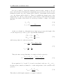
5.2 Kinetic traces analysis methods . . . . .
5.2.1 Autocorrelation analysis . . . . .
5.2.2 Trace-histogram analysis . . . . .
5.2.3 Comparison . . . . . . . . . . . .
5.3 Experimental . . . . . . . . . . . . . . .
5.3.1 Sample preparation . . . . . . . .
5.3.2 Measurement . . . . . . . . . . .
5.4 Influence of a nearby thin Au film on the
5.4.1 Influence on Γ21 . . . . . . . . . .
5.4.2 Influence on kof f . . . . . . . . .
5.4.3 Influence on kon . . . . . . . . . .
5.5 Conclusions . . . . . . . . . . . . . . . .
.
.
.
.
.
.
.
.
.
.
.
.
.
.
.
.
.
.
.
.
.
.
.
.
.
.
.
.
.
.
.
.
.
.
.
.
.
.
.
.
.
.
.
.
.
.
.
.
.
.
.
.
.
.
.
.
. . . . . . . . . . . . . . .
. . . . . . . . . . . . . . .
. . . . . . . . . . . . . . .
. . . . . . . . . . . . . . .
. . . . . . . . . . . . . . .
. . . . . . . . . . . . . . .
. . . . . . . . . . . . . . .
. . . . . . . . . . . . . . .
electronic transition rates
. . . . . . . . . . . . . . .
. . . . . . . . . . . . . . .
. . . . . . . . . . . . . . .
. . . . . . . . . . . . . . .
6 Photoluminescence blinking of Zn0.42 Cd0.58 Se nano-crystals
6.1 Brief Introduction and current status . . . . . . . . . . . . . .
6.2 Experimental . . . . . . . . . . . . . . . . . . . . . . . . . . .
6.2.1 Sample preparation . . . . . . . . . . . . . . . . . . . .
6.2.2 Measurement . . . . . . . . . . . . . . . . . . . . . . .
6.3 QD kinetic traces . . . . . . . . . . . . . . . . . . . . . . . . .
6.3.1 General characteristics . . . . . . . . . . . . . . . . . .
6.3.2 Effect of the excitation intensity . . . . . . . . . . . . .
6.4 Modelling the QDs blinking . . . . . . . . . . . . . . . . . . .
6.4.1 Blinking model . . . . . . . . . . . . . . . . . . . . . .
6.4.2 Monte-Carlo procedure . . . . . . . . . . . . . . . . . .
.
.
.
.
.
.
.
.
.
.
.
.
.
.
.
.
.
.
.
.
.
.
.
.
.
.
.
.
.
.
.
.
.
.
.
.
.
.
.
.
.
.
.
.
57
57
59
59
60
62
62
64
66
68
68
71
75
78
81
.
.
.
.
.
.
.
.
.
.
.
.
.
85
85
88
88
90
95
97
99
100
101
102
103
105
106
109
. 110
. 112
. 112
. 113
. 114
. 114
. 115
. 123
. 124
. 124
CONTENTS
6.5
iii
6.4.3 Simulated blinking . . . . . . . . . . . . . . . . . . . . . . . . 127
Conclusions . . . . . . . . . . . . . . . . . . . . . . . . . . . . . . . . 132
7 Light scattering from single metallic nano-structures
7.1 Introduction . . . . . . . . . . . . . . . . . . . . . . . . . .
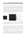
7.2 Light scattering of individual colloidal gold nanoparticles .
7.2.1 Experimental . . . . . . . . . . . . . . . . . . . . .
7.2.2 Images of colloidal gold nanoparticles . . . . . . . .
7.2.3 Spectra of colloidal gold nanoparticles . . . . . . .
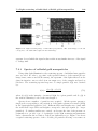
7.3 Light scattering of individual C-shaped gold nanoparticles
7.3.1 Experimental . . . . . . . . . . . . . . . . . . . . .
7.3.2 Images and spectra of C-shaped gold nanoparticles
7.4 Conclusions . . . . . . . . . . . . . . . . . . . . . . . . . .
.
.
.
.
.
.
.
.
.
.
.
.
.
.
.
.
.
.
.
.
.
.
.
.
.
.
.
.
.
.
.
.
.
.
.
.
.
.
.
.
.
.
.
.
.
8 Summary
A Set-up control and data acquisition software
A.1 AD-Basic routines . . . . . . . . . . . . . . . . . . . . . . . . . . . .
A.2 Igor routines . . . . . . . . . . . . . . . . . . . . . . . . . . . . . . .
A.3 C++ routines . . . . . . . . . . . . . . . . . . . . . . . . . . . . . .
135
. 135
. 136
. 136
. 137
. 139
. 140
. 140
. 142
. 143
145
149
. 149
. 163
. 180
List of tables
187
List of figures
191
Abbreviations
193
Bibliography
195
Acknowledgements
205
Curriculum Vitae
207
Chapter 1
Introduction
In 1974, Fleischmann and co-workers [1] wanted to perform experiments on pyridine by combining electrochemistry and Raman spectroscopy. In order to increase
the Raman signal, they deposited the pyridine onto a roughened silver electrode.
The idea was to increase the surface area of the electrode and therefore the amount
of adsorbate on the sample. It worked; the Raman signal was indeed greatly increased. Three years later, Jeanmaire and van Duyne [2], as well as Albrecht and
Creighton [3], recognized independently that the large intensities observed could
not be accounted for simply by the increase in the number of scatterers present.
They proposed that an enhancement of the scattered intensity occurred in the adsorbed state. Already at that time a surface plasmon enhancement mechanism of
the scattered intensity was proposed [3, 4]. Since then, this effect was called surface
enhanced Raman scattering (SERS) and captured the attention of chemists, physicists and engineers from around the world. It is not hard to see the motivation for
such interest. The effect was large, completely unexpected, difficult to understand
and of enormous practical utility if it could be understood and exploited.
The investigation of the SERS still continues and the understanding of the phenomenon has increased considerably. Nowadays, it is accepted that the SERS effect
is caused by greatly enhanced electromagnetic fields generated by surface plasmon
resonances (SPR) in certain hot spots of the rough substrate. At this point, it is
important to note that such strong and localized electromagnetic fields do not only
find applications in the SERS. For example, they can also be employed in optical
tweezers and to modify radiative rates in a variety of processes such as molecular
fluorescence. Recent advances in microscopy have made it possible to use single
metallic particles as SERS substrates and to obtain the Raman spectra of single
molecules adsorbed on them [5].
Almost simultaneously, the field that is today called nanotechnology developed,
and thanks to that, it is possible to produce an enormous variety of structures in
the sub-micrometer scale. In particular, metallic structures with nanometer size
and different shapes can be manufactured and their surface plasmon resonances can
2
Introduction
be tailored. These days, it is possible to think of a structure composed of metallic nanoparticles and a chromophore (or Raman scatterer) in a defined geometry in
order to produce an ultra effective marker or to imagine a metallic nano-structure engineered to function as a nano-optical-tweezers. Even though such a nano-structure
cannot be fabricated in a controlled manner yet, several research groups around the
world are working on it, and it should not be long until this is achieved. The aim
of this Ph.D. thesis is to settle the basis for the quantitative assessment of effects in
individual such functional nano-structures.
The first step taken was the design and construction of a scanning confocal optical microscope (SCOM) that allows to measure, from the same diffraction-limited
spot, time-resolved fluorescence and SERS with single molecule sensitivity and light
scattering with highest resolution achievable with a far-field method (chapter 2).
This instrument allows to investigate the surface plasmon resonances of individual metallic nanoparticles (chapter 7) and their influence on the Raman scattering
and/or fluorescence processes.
Then, a model system was sought to realize the first systematic study. Surface
plasmon resonances can be excited not only in metallic nanoparticles but also in
planar surfaces. Such a simple geometry, although it provides a relatively small
field enhancement, represents a very convenient platform for systematic studies because it is easy to fabricate, their geometric parameters can be controlled and a
complete mathematical modelling is possible. The first studies were performed with
fluorophores placed at a controlled separation distance from a gold film. The influence of the locally enhanced surface plasmon electromagnetic field on molecular
fluorescence was investigated on a single molecule level.
First, a theoretical model was set-up to calculate the fluorescence signal of a
single molecule in a plane layered system, including the electric field distribution in
the focus of the SCOM and the emission rates of a chromophore (chapter 3). Second,
the excitation and emission of single molecule fluorescence through a thin gold film
was investigated experimentally and modelled (chapter 4). Third, the influence of
the nearby gold film on the electronic transition rates responsible of the fluorescence
process was studied (chapter 5).
If fluorescent markers are being considered, nanometer-size colloidal semiconducting crystallites, also known as quantum dots (QD) cannot be ignored. Since the
middle 70s, the QDs have provoked a tremendous fundamental and technical interest. Owing to their size-dependent photoluminescence which is tunable across the
complete visible spectrum, the QDs find application as light-emitting devices, lasers,
and biological labels. However, the emission process in semiconducting QDs involves
very complicated processes and the emitting state remains controversial. Recently,
the advent of QD studies on a single dot level brought a new complication: the QDs
present extremely complicated emission fluctuations that could not be explained
until now. Even though surface enhancement effects were observed on QDs [6], the
lack of knowledge about the blinking mechanism prevents an effective exploitation
3
of the effect. It is fundamental to understand the blinking of QDs before trying
to improve their performance by other means such as locally enhanced fields. The
photoluminescence blinking of QDs was experimentally investigated and modelled
in order to gain some insight into the underlying physical processes (chapter 6).
The last experimental tool necessary for the investigation of field enhancements
on a single nano-structure level is the capability of studying SPRs in individual
metallic nano-particles. In order to fill this need, the home built SCOM was adapted
for light scattering measurements and its performance was tested on spherical and
C-shaped gold particles (chapter 7).
Chapter 2
The fluorescence and light
scattering confocal microscope
A scanning confocal optical microscope (SCOM) was designed and constructed
to perform local studies of fluorescence and light scattering, with diffraction-limited
spatial resolution and single photon sensitivity. This instrument allows working
with many different experimental schemes. The most distinctive characteristic is
the possibility of measuring fluorescence and scattered light from the same focal
spot.
The sections of this chapter are dedicated to detailed description of the microscope. The first section explains the confocal principle. The second section describes
the different components and their functions. Finally, the last two sections explain
how to properly align and operate the instrument.
2.1
The confocal principle
An ideal optical microscope would examine each point of the specimen and measure the amount of light scattered or absorbed by that point1 . However, if many of
such measurements were performed simultaneously, every point in the image plane
would be clouded by aberrant rays of scattered light coming from other points of
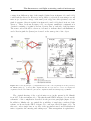
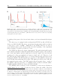
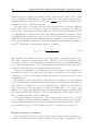
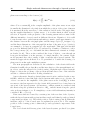
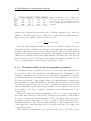
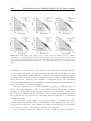
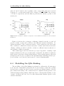
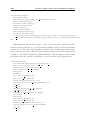
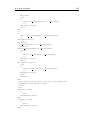
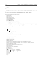
the sample. Marvin Minsky [7, 8] found in 1955 a simple and elegant solution for
this problem: the confocal arrangement (see figure 2.1).
In the first place, it is possible to illuminate only one point of the specimen at a
time by using a microscope objective to focus the light spread by an aperture pinhole
(illumination pin-hole in figures 2.1.a and 2.1.b). As a consequence, the amount
of light in the specimen is reduced by orders of magnitude, without reducing the
focal brightness at all (fundamentally important to prevent photo-bleaching in single
molecule fluorescence experiments). Still, due to multiple scattering, some extra rays
1
In this context ”point” means a diffraction limited spot.
6
The fluorescence and light scattering confocal microscope
coming from different points of the sample (dashed rays in figures 2.1.a and 2.1.b)
could reach the detectors. However, it is possible to reject those rays using a second
microscope objective to image on the same (confocal) point of the specimen, a second
pinhole aperture (detection pinhole in figures2.1.a and 2.1.b) placed in front of the
detector. Then, as shown in figure 2.1.a, an elegant, symmetric configuration is
obtained consisting of a pinhole and an objective lens on each side of the specimen.
The term confocal should be clear now, it is used to indicate that both illumination
and collection pinholes (lenses) are focused on the same point of the object.
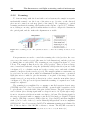
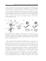
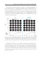
Figure 2.1: Confocal principle. c) Original sketches of the confocal principle from the patent by
M. Minski (1957) [7]. a) and b) The original sketches are reproduced to better accompany the
explanation in the text. FIG.2 in c) shows the original mechanical scanning stage by Minski.
The original drawing of the confocal microscope in the patent by M. Minski,
from 1957, is shown in figure 2.1.c. The sketch named FIG.1 in figure 2.1.c shows the
schematic of the configuration described in the previous paragraph (figure 2.1.a).
In addition, Minsky also recognized the possibility of employing a reflected light
scheme, as shown in the FIG.3 of figure 2.1.c, and reproduced in figure 2.1.b. In
this case, only a single lens on one side of the specimen is used, and a half-silvered
mirror separates the entering and exiting rays. This arrangement is equivalent to
2.1 The confocal principle
7
the symmetric one in terms of resolution but much simpler in terms of alignment
and operation. The price to pay for the simplicity is the fourfold brightness loss
due to the beam splitter. However, in fluorescence measurements, the efficiencies
of both configurations are similar because a dichroic filter can be used to spectrally
separate the excitation and fluorescence light.
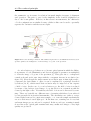
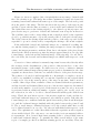
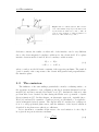
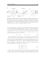
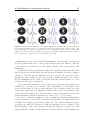
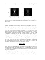
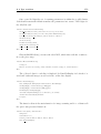
Figure 2.2: Confocal image formation. The diffraction patterns of both illumination and detection
aperture pinholes are multiplied to form the image of a point of the specimen.
A confocal microscope behaves as a coherent optical system in which the diffraction patterns of both (illumination and detection) pinhole apertures are multiplied
to form the image of a point of the specimen [9]. This gives rise to a sharpened
central peak and weak outer rings with the consequent increase in resolution (see
figure 2.2). Even though the improvement in resolution may at first sight seem to
contravene the basic limits of optics, it can be explained by a principle described
by Lukosz [10, 11], which states that resolution may be improved at the expense
of field of view. In the case of a confocal microscope, the field of view is reduced
by means of the back projected image of a point detector in conjunction with the
focused point light source. Nevertheless, the field of view can be increased by scanning. There are basically two different ways of scanning which have been achieved
by various methods in practical instruments. The alternatives are either to scan a
focused light beam across a stationary sample, or to scan the sample mechanically
across a stationary focused light spot. In the first case, scanning can be very fast
and many images per second can be acquired. In the second case, scanning is much
slower but as the optical path remains stationary, undistorted images of very high
quality are produced.
8
The fluorescence and light scattering confocal microscope
2.2
Description of the home built confocal microscope
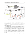
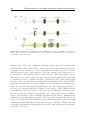
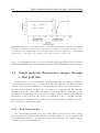
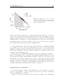
Figure 2.3 shows schematically the different components of the home-built SCOM
set-up and helps as a guide for the detailed descriptions presented in the next sections
of this chapter.
A number of light sources can be employed to obtain either monochromatic or
white light illumination. In every case, the light provided by the source is coupled
into a single-mode optical fiber to obtain a point-like light source equivalent to
the illumination pin-hole described in the previous section. Light coming out of
the fiber is collimated to form the illumination beam. With the help of a dichroic
mirror or a beam splitter, the illumination beam is directed to a high numerical
aperture microscope objective that focuses it onto the sample. Light coming from
the sample is collected by the same objective and directed by a mirror to the single
photon detectors and/or the spectrograph. In order to acquire an image or to study
different regions, the sample can be mechanically scanned over the focused beam by
means of a piezoelectric xyz stage. Furthermore, although not included in figure 2.3,
the microscope is equipped with a second single mode fiber aligned in the confocal
system that can be coupled to any of the light sources. This allows to perform
simultaneous illumination with two wavelengths. In the following, for simplicity and
because both fibers are equivalent, only one fiber is considered.
The set-up is very flexible. Different modes of illumination and detection can be
implemented to perform a variety of studies, such as fluorescence, Raman2 and light
scattering measurements.
Following, all the components of the set-up and their functions are described
in detail. Section 2.2.1 describes the illumination, section 2.2.2 the scanning and
section 2.2.3 the detection. The time correlated single photon counting unit is described in section 2.2.4, and the computer control in section 2.2.5.
2.2.1
Light sources and illumination
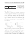
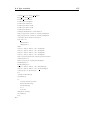
A variety of light sources can be adapted to the microscope. Table 2.1 lists the
principal characteristics of the light sources used in the experiments presented in
this dissertation.
Light provided by any of these sources is focused with a suitable microscope
objective and coupled into a single-mode optical fiber. For this, the fiber is mounted
on a positioning xyzθφ stage (New Focus Inc.) with sub-micrometer precision. When
using laser light, a λ/2 and a λ/4 plates (OWIS GmbH ) are placed before the light
is coupled into the fiber and adjusted to compensate its polarization effects. Two
2
Although no Raman scattering measurements were performed in this work, the changes in
set-up configuration required to allow such measurements are straight forward
2.2 Description of the home built confocal microscope
9
Figure 2.3: Schematic of the home-built confocal microscope
types of fibers were used: standard single-mode fibers for 635 or 515 nm (Thor Labs
Inc.) or photonic crystal fibers (Endless Single Mode, Blaze Photonics Ltd.); the
latter has the characteristic of acting as a single mode fiber in a wide range of
wavelengths [12, 13]. The pure-Gaussian-mode (TEM00) light coming out of the
fiber is collimated with a 150 mm focal length achromatic lens (OWIS GmbH ) to
form the illumination beam.
The illumination beam is aligned with the main optical axis of the microscope
(for alignment details please refer to section 2.3), and its diameter is adjusted with a
diaphragm. If the experiment requires annular illumination, a blocking disc can be
introduced in the axis of the illumination beam. The diaphragm and the blocking
disc should be placed as close as possible to the microscope objective in order to
minimize the optical path to the focus and therefore the diffraction effects from
the borders of the pin-hole or the disc. Furthermore, it is advisable to minimize
the number of optical elements between the fiber tip and the microscope objective
because small distortions of the illumination beam can produce important effects in
the focus.
A 100×, 1.4 NA, oil immersed microscope objective (Plan-Apo, Nikon GmbH ) is
10
The fluorescence and light scattering confocal microscope
Table 2.1: Light sources. CW stands for continuous wave and FWHM for full width at half
maximum.
used to focus the illumination beam onto the samples. The microscope objective is
mounted on a xyz stage with micrometer precision.
Fluorescence measurements
For fluorescence measurements laser light is used. Line pass filters (Omega Optics Inc.) are used to refine the illumination wavelength and a dichroic mirror (AHF
AG) is used to direct the illumination beam to the microscope objective and to
separate the excitation from the fluorescence light.
Light scattering measurements
For light scattering measurements, annular illumination (see next subsection) is
combined with a reduced detection beam. Instead of a dichroic mirror, a 50/50 beam
splitter (OWIS GmbH ) is used to direct the illumination beam to the microscope
objective and to separate the excitation from the fluorescence light.
Focusing angles and annular illumination
The TEM00 light provided by the single mode fiber is collimated with an achromatic lens with minimized spherical aberration. Therefore, the illumination beam
2.2 Description of the home built confocal microscope
11
can be considered as being formed by plane waves. A microscope objective is an
optical system that produces aplanatic images; i.e. axially stigmatic and obeying
the sine condition [14] (null spherical aberration). Hence, the plane waves of the
illumination beam are transformed by the objective in spherical waves with the center at the Gaussian focus. The maximum focusing angle (θN A ) is determined by the
numerical aperture (NA) of the objective and the refractive index of the focusing
medium (nglass ) according to:
θN A = arcsin
NA
nglass
(2.1)
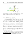
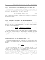
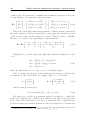
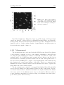
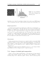
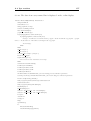
Figure 2.4: Focusing angles. Geometric representation of the focal sphere of the microscope
objective and the focusing angles for the cases of: a) Complete illumination of the rear lens of the
objective, b) Annular illumination.
The radius of the focal sphere R (see figure 2.4.a) is determined by the radius of
the rear lens of the objective Rrl , and the refractive index of the focusing medium
(nglass ):
R=
Rrl
Rrl nglass
=
sin θN A
NA
(2.2)
Thus, if the rear lens of the objective is illuminated with an annular beam of
outer radius R1 and inner radius R2 , the maximum and minimum focusing angles,
θ1 and θ2 respectively (see figure 2.4.b), are given by:
R1,2
R1,2 N A
θ1,2 = arcsin
= arcsin
(2.3)
R
Rrl nglass
The microscope objective used in all the experiments presented in this dissertation has a NA=1.4 and the refractive index of the glass slides (and the matching oil)
is nglass =1.503, which leads to a maximum focusing angle of 68.6◦ . The rear lens
of the objective has a radius of 4.45 mm, therefore the radius of the effective focal
sphere is 4.78 mm.
12
The fluorescence and light scattering confocal microscope
2.2.2
Scanning
To form an image with the home-built confocal system, the sample is stepwise
mechanically scanned over the focus of the microscope objective, as the detected
photons are counted at each step (pixel of the image). In comparison to optical
scanning, mechanical scanning offers quality at the expense of speed [15]3 . Furthermore, having no moving optical elements makes it easier to adapt new elements in
the optical path, and also makes the alignment more stable.
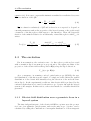
Figure 2.5: Scanning process. The parameters used to control the scanning are listed on the
right.
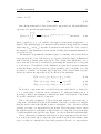
Four parameters are used to control the scanning: the initial position, the scanning range, the number of pixels (the same for both dimensions), and the pixel time
(counting time at each pixel). The scanning process, depicted in figure 2.5, is as
follows. The sample is first moved to the initial position. Then, it is moved stepwise, forward and backward, along the (arbitrarily called) x direction (arrows 1 and
2 in figure 2.5), to a definite extent set by the scanning range, and with a definite
number of steps set by the number of pixels. The sample remains a certain time, set
by pixel time, at each position, while it is illuminated and fluorescence or scattered
light photons are counted to give the intensity of one pixel of the image. Next, the
sample is moved one step in the y direction in order to start the next x-line (arrow
3 in figure 2.5). The process is repeated until the scanning of a squared area of the
sample is completed.
The scanning is accomplished by a computer controlled xyz-piezoelectric stage
(TRITOR 101 CAP, Jena Piezosystems GmbH ), operated with a capacitive closed
loop feedback to correct the drift of the piezoelectric drivers. The piezoelectric stage
can be driven (via a driving signal with a voltage from 0 to 10 V) through a range
from 0 to 80 µm in each direction with a resolution of 0.5 nm. The driving signal for
the stage is generated with a computer controlled 15-bit Analog to Digital / Digital
to Analog (AD/DA) converter (ADWin-light-16, Jäger GmbH ), and then amplified
with 3 (one for each of the x, y, and z channels) independent low-noise amplifiers
(ENV40CAP, Jena Piezosystems GmbH ). The minimum scanning step is limited by
the 15-bit resolution of the AD/DA converter to 2.4 nm. The AD/DA converter is
3
For details about the different scanning methods, see the book by T. Wilson [16]
2.2 Description of the home built confocal microscope
13
equipped with a local processor and local memory that enable to perform real-time
measurements with a resolution of 25 ns, regardless of the speed of the controlling
computer.
The data acquisition also is accomplished by the same AD/DA converter. For
each pixel of an x-scanned line (forward and backward), the position, the counts, and
the starting and final counting times, are stored in the local memory of the AD/DA
converter. Then, the sample is moved in the y direction, and before starting the next
x-line, all the information is transferred to the controlling computer. Like this, the
counting times are measured with a resolution of 25 ns. The so collected data has the
information corresponding to two images of the same region: one forward-scanned
and the other backward-scanned. The individual images need to be extracted from
the complete data.
Forward and backward images from the collected data
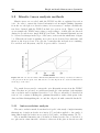
While scanning at a reasonable speed4 (∼ 0.5 − 2 lines/s), the piezoelectric stage
response in the x direction is delayed with respect to the driving signal. In the y
direction, due to the time necessary for the data transfer, the piezoelectric stage has
sufficient time to reach the set position.
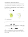
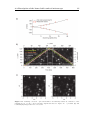
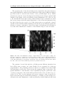
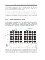
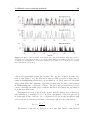
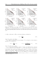
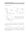
Figure 2.6: Scanning delay. Complete data collected to construct backward and forward images
of 5 × 5 µm2 , 128 × 128 pixels each. Extra pixels were scanned in the x-direction in order to discard
the pixels corresponding to the delay near the direction inversion points.
4
The scanning speed here mentioned is an actual speed in µm/s, then it relates the scanning
range, the pixel-time and the number of pixels. A reasonable value for the scanning rate is for
example 40 µm/s, corresponding to an image of 10 × 10 µm2 , with 250 × 250 pixels and a collection
time of 1 ms
14
The fluorescence and light scattering confocal microscope
Figure 2.6, shows a complete (320 × 128 pixels) fluorescence image obtained with
the confocal microscope. The image has a mirror symmetry because it is formed by
scanning forward and backward the same region of the sample. The left and top axis
show the pixels of the image. The left axis shows the x-position of the stage in µm,
and the bottom axis the time necessary to scan forward and backward an x-line.
The dashed-line curve is the driving signal (i.e. the desired x position) sent to the
piezoelectric stage to perform a forward and backward scan along the x direction.
The solid-line curve is the corresponding monitor signal provided by the capacitive
closed loop, which is meant to report the actual position of the piezoelectric stage.
The delay between the driving signal and the position of the stage reported by the
capacitive loop can be clearly seen by comparing the driving to the monitor signals.
If the individual forward and backward images are constructed by taking into
account the driving signal (i.e. dividing the image in figure 2.6 in two through the
center), the images present two artifacts. First, due to the inertia of the piezoelectric
drivers at the direction inversion points, the images appear blurred at one edge (the
forward image on the left and the backward image on the rigt side). Second, due to
the total delay, the forward and backward images are shifted with respect to each
other.
Correction of these artifacts is extremely important because they directly affect
the accuracy in the determination of the position of fluorescent dyes or any other
measurable feature on the sample. For this reason, in order to construct consistent
forward and backward images that permit proper position determination, the data
acquisition software has to take into account the behavior of the piezoelectric stage.
The software code can be found in appendix A.3. In principle, a complete correction
could be accomplished by taking into account the capacitive monitor signal which
is supposed to report the actual position of the stage at any time. Such correction
consists of three steps. First, a number of lines are scanned with the set parameters,
and the forward and backward linear regions of the monitor signal are determined,
as well as the number of invalid pixels at the inversion points. Second, a new scan
is performed with an additional number of pixels, equal to the invalid pixels, in
the x direction, in order to be able to discard them and still keep the desired scan
range. Third, the new linear regions of the monitor signal are found, and the forward and backward images are constructed only with those pixels. Like this, the
forward images are constructed with the pixels between the points A and B in figure
2.6, and the backward images similarly with the pixels between the points C and
D. The so made images, delimited in figure 2.6 by the vertical white lines, would
not be blurred anymore at one edge. Yet, they are still shifted with respect to each
other. The explanation for this extra shift is that the capacitive monitor signal is
electronically delayed. The only way to account for this, is via an empirical calibration parameter. It is observed that faster scanning leads to a larger shift between
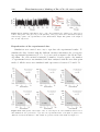
forward and backward images. To quantify the shift, several images of the same
region of a sample, produced at different scanning speeds, are necessary. Then, the
2.2 Description of the home built confocal microscope
15
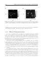
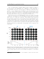
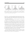
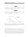
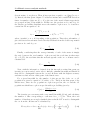
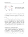
Figure 2.7: Scanning correction. a) Position shift of an arbitrary feature as a function of the
scanning speed. b) the corrected monitor signal was added to figure 2.6. c) forward (F) and
backward (B) images after the corrections.
16
The fluorescence and light scattering confocal microscope
position of one feature can be followed, on both forward and backward images, as a
function of the scanning speed. In this manner, as shown in figure 2.7.a, the position
shift vs. scanning speed can be fitted with a polynomial function and the empirical
correction parameters are obtained. Using the correction parameters, the monitor
signal can be corrected to give the actual position of the sample. In figure 2.7.b the
same data of figure 2.6 is shown, but this time the empirically corrected monitor
signal is shown. Then, the pixels corresponding to the forward and backward linear
regions of the corrected monitor signal are found (following the algorithm detailed
in the appendix A.3), and the forward and backward images are constructed. These
images, delimited in figure 2.7.b by the vertical white lines and shown in more detail in figure 2.7.c, are consistent; the average shift between forward and backward
images is smaller than one pixel size.
2.2.3
Detection
The detection channel can be adapted to different experimental designs. In the
experiments presented in this dissertation, fluorescence and light scattering measurements were performed and the corresponding detection schemes are described
below.
Common to all the detection schemes is that light collected from the sample is
directed to the detection channel via a silvered mirror (OWIS GmbH ; figure 2.3).
Then, the light is focused with a 100 mm focal length achromatic lens (OWIS GmbH )
into a 150 µm confocal (to the microscope objective) pinhole (New Focus Inc.), and
collimated again with a second 100 mm focal length achromatic lens (OWIS GmbH ).
For imaging, this collimated beam is directed and focused with another 100 mm
focal length achromatic lens (OWIS GmbH ) to one of the single photon counting
detectors. For spectrally resolved measurements, the detected collimated beam is
directed to the transmission grating spectrograph. Further information about the
single photon detectors and the transmission grating spectrograph is given below.
In addition, the microscope is equipped with an ocular (Axiomat Plan W 10×25,
Carl Zeiss Germany) that can be used for focusing (see section 2.3.4) and visual
inspection of the samples.
Other optical elements such as polarizing beam splitters, or dichroic mirrors can
be installed in the detection channel according to the requirements of a particular
experiment.
The photon counting for imaging is accomplished by a digital counter of the
same AD/DA converter that controls the scanning. This counter only requires TTL
(Transistor-Transistor Logic) input pulses. Therefore, any detector can be adapted
to the set-up as long as its output signal is (or is transformed to) a TTL pulse.
2.2 Description of the home built confocal microscope
17
Fluorescence measurements
For fluorescence measurements, in order to remove residual excitation light not
filtered by the dichroic mirror, suitable long-pass (Omega Optics Inc.) and notch
(Notch Plus, Kaiser Optical Systems Inc.) filters are placed in the detection channel.
Light scattering measurements
For light scattering measurements, no filters are used. Instead, annular illumination is employed and the outer part of the detected beam (which under ring
illumination conditions contains mainly reflected light) is blocked by a diaphragm
so that only scattered light can reach the detectors (see figure 2.8).
Figure 2.8: Light scattering set-up configuration. The dashed line shows the path followed by
the reflected light.
It is also possible to work with the inverse configuration; i.e. illuminate with a
reduced beam and block the inner part of the detection channel with an appropriate
disc.
The single photon detectors
The set-up counts with two different single photon detectors: an Avalanche Photo
Diode (APD) and a Photo-Multiplier Tube (PMT). Both detectors can be used for
imaging and time correlated measurements. Table 2.2 shows the principal technical
characteristics of each detector.
The APD provides TTL pulses that can be directly counted by the AD/DA
converter. The PMT instead provides very weak, fast and negative pulses. The
easiest way to transform this signal into a TTL pulse is by means of an Oscilloscope.
18
The fluorescence and light scattering confocal microscope
Table 2.2: Single photon counting detectors. APD: avalanche photo diode. PMT: photo multiplier
tube. CPS: counts per second. λ: wavelength. FWHM: full width at half maximum. All the
quantities were corroborated in the laboratory, except the ones marked with * which are taken
from the manufacturer specifications.
The 50 Ω input channel of a 300 MHz oscilloscope (Tektronix 2465 ) is supplied with
the PMT signal. Once the triggering is adjusted, the monitor output of the oscilloscope provides one TTL for each PMT pulse. The power supply, the Peltier
cooling, and the gain of the PMT are computer controlled with a controller and a
software specifically designed for this detector (DCC-100, Becker und Hickl GmbH ).
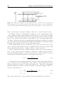
The transmission grating spectrograph
In order to measure single molecule fluorescence and light scattering spectra,
a transmission grating spectrograph was adapted to the set-up. The spectrograph
consists of a volume phase holographic (VPH) transmission grating (HVG-590 and
HVG-690, Kaiser Optical Systems Inc.), a photo objective (35 mm, f1.4, Nikon Inc.)
and a high quantum efficiency, charge-coupled device (CCD) camera (SensiCam QE,
PCO Imaging GmbH ). Table 2.3 presents the relevant technical information for these
components.
The collimated detected beam is directed to the VPH grating either by a silvered
mirror or by a beam splitter. Light is diffracted by the VPH grating at angles
according to classical diffraction and the energy distribution is governed by the
Bragg condition. The photo objective focuses the spectrally dispersed light into a
line of the CCD sensor of the camera.
The spectral ranges covered by the HVG-590 and HVG-690 gratings are from
390 to 790 nm and from 500 to 800 nm, respectively. The size of the detectable
spectral range depends on the angular dispersion of the grating, the focal length
2.2 Description of the home built confocal microscope
19
Table 2.3: Spectrograph components. The angular dispersion of the gratings were measured in
the laboratory. The other information is presented as provided by the manufacturer.
and the diaphragm aperture of the photo objective, the diameter of the detected
beam (8.9 mm), and the size of the CCD sensor. The spectral resolution is directly
determined as the ratio of the spectral range and the number of pixels of the CCD
sensor5 . For the mentioned objective and CCD camera, the maximum detectable
spectral range is 260 nm with a resolution of 0.19 nm with the HVG-650 grating,
and 340 nm with a resolution of 0.25 nm with the HVG-590 grating. The position
of the detectable spectral range can be shifted simply by moving the CCD camera.
2.2.4
Time Correlated Single Photon Counting
Time Correlated Single Photon Counting (TCSPC) [17] has been one of the best
ways of measuring fluorescence decay times since the method was conceived in 1961
by Bollinger and Thomas [18].
TCSPC is based on the detection of single photons and the computation of their
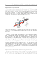
individual detection times. Figure 2.9 helps to explain the TCSPC working principle.
The excitation light should be pulsed at such frequency that the fluorescence is
allowed to decay completely in between pulses. In addition, the detected fluorescence
intensity should be low enough so that the probability of detecting two photons in
between pulses is negligible. The latter condition is naturally fulfilled in the case
of single molecule fluorescence measurements. Under these conditions, every time
a photon is detected, the time elapsed from the last excitation pulse is computed
(mic-t in figure 2.9.a). Then, if the laser pulses are narrow enough in comparison to
the typical fluorescence decay time, the fluorescence decay curve is directly obtained
5
The photo objective focuses the monochromatic beams dispersed by the grating into diffraction
limited spots with a size ranging from 1.9 to 3.5 µm, depending on the wavelength. The pixel size
of the CCD sensor is 6.75 µm.
20
The fluorescence and light scattering confocal microscope
Figure 2.9: Time correlated single photon counting principle. a) The curve represents the excitation light pulses, and the short vertical lines represent detected fluorescence photons. For each
detected photon, the time from the beginning of the experiment (Mac-t) and the time from the last
excitation pulse (mic-t) are determined. b) The fluorescence decay curve is obtained by computing
a histogram of the mic-t times.
by making a histogram of the detected mic-t times, as shown schematically in figure
2.9.b.
The microscope is equipped with an independent TCSPC module (SPCM-630,
Becker und Hickl GmbH ). The device can measure the mic-t times with a resolution
of 12 ps, up to a rate of 8 MHz 6 . Furthermore, the TCSPC unit also records, for
every detected photon, the detection time from the beginning of the experiment
(Mac-t in figure 2.9) with a resolution of 50 ns.
The TCSPC module needs only two input signals. The pulse-train signal from the
laser, which is typically a sinusoidal signal with a frequency equal to the repetition
rate of the laser pulses, and the single photon detector signal. In both cases the
signals need to have an amplitude in between -50 mV and -1 V. Therefore, both
the APD and the PMT signals need to be treated with specific electronics before
feeding the TCSPC. The APD signal is processed by a router (HRT-82, Becker und
Hickl GmbH ) that transforms the positive TTL pulses provided by the APD into
the required negative pulses. The PMT signal is already negative but too weak for
the TCSPC, therefore it needs to be amplified with a 26 dB, broadband (5 kHz 1.6 GHz) amplifier (HFAC-26, Becker und Hickl GmbH ).
The ultimate time resolution for the determination of fluorescence lifetimes is
usually limited by one of the following two factors. First, the width of the laser
6
In fact, the TCSPC unit takes advantage of the low intensity conditions. It determines the
time from the photon detection until the next excitation pulse, and calculates the mic-t time later
by difference. In this manner, the TCSPC unit performs the time calculation only when a photon is
detected and not for all the pulses. This is justified by the fact that for usual laser pulses repetition
rates (∼ 50 MHz), the probability of detecting photons in consecutive pulses is negligible (detection
rates for a single molecule are ∼ 0.05 MHz).
2.2 Description of the home built confocal microscope
21
pulses which is around 300 ps for both pulsed lasers. Second, the reproducibility
of the rising cant of the detector pulses. The latter is important due to the zero
crossing method used by the TCSPC unit to determine the temporal position of the
signals; further details can be found in the TCSPC operation manual [19].
2.2.5
Computer control
Several functions of the microscope are computer controlled, either via commercially available software or by home made programs developed during the work for
the present dissertation. This section describes how the computer control of the different functions is organized. Details about the operation can be found in section 2.4.
Scanning and confocal data acquisition control
The operation of the piezoelectric stage, as well as the data acquisition for all
types of imaging, is accomplished with the AD/DA converter. The AD/DA is computer controlled with a home made software that consists of three parts. The first
part consists of routines that operate at the lowest level, directly on the local CPU
and memory of the AD/DA converter and perform the basic operations, such as
scanning a line or counting photons at one pixel. These routines were programmed
in a specific computer language (ADBasic [20]) provided by the AD/DA manufacturer. The second part is the PC user interface. With this software, the user can
set the scanning parameters, as well as observe on-line the collected data and save
it in an appropriate format. The PC user interface was programmed in Igor [21] in
order to take advantage of Igor’s built-in capabilities for data treatment. Finally, the
third part consists of a set of routines required for the communication between the
PC user interface and the local CPU of the AD/DA converter. These routines were
programmed in C++. The code of all these programs is presented and described in
the appendix A.3.
CCD camera and spectra acquisition control
The CCD camera can be controlled with specific software provided by the manufacturer, and details about the operation can be found in the operation manual of
the camera [22]. All the relevant parameters for the operation of the CCD camera
can be controlled, such as the active region of the CCD sensor and the collection
time. It is also possible to record up to 9999 frames as a function of time with
a minimum collection time of 1 ms (maximum repetition rate of 1000 spectra per
second).
22
The fluorescence and light scattering confocal microscope
TCSPC unit control
The TCSPC unit has its control software control provided by the manufacturer;
details about the operation can be found in the user manual of the TCSPC module [19].
2.3
Alignment
The complete alignment of the set-up can be separated in four parts. The first
one is the in-coupling of light (provided by any of the light sources) to the single
mode fiber. The second is the collimation of the light provided by the fiber and the
alignment of the illumination beam. The third one is the alignment of the dichroic
mirror or beam splitter and the microscope objective. Finally, the fourth part is
the alignment of the detection optics and detectors. In the present section, the four
alignment procedures are explained.
2.3.1
Light coupling into the single mode fiber
A fundamental pre-requisite for an effective coupling of light into the single mode
fiber is that both tips of the fiber have to be be sharply cut. For this, it is first
necessary to remove the polymer cladding7 , and then cut the tips with a diamond
fiber cutter (RXS Kabelgarnituren GmbH ).
The process of in-coupling light into the single mode optical fiber consists of two
steps. First, light provided by any of the sources has to be focused onto the fiber tip.
Second, the fiber position needs to be adjusted in order to maximize the in-coupled
light. The different light sources have different focusing requirements as explained
below. To couple the focused light into the fiber one should first position the fiber
tip approximately in the focus by moving the tip in x, y and z directions, until light
scattered by the fiber tip is observed. Then, iterative adjustments of the fiber tip
position in x, y, and z directions, should be done as the light intensity coming out
of the fiber is monitored. Once the x, y and z positions are optimized, further fine
adjustments of the tilting (θ and φ) of the fiber can be done.
When using laser light, in order to control the polarization of the illumination
beam, a λ/2 and a λ/4 plates are placed between the laser and the fiber. The angular
position of the plates have to be adjusted in order to produce a polarization state in
the laser beam such that, after the polarization effects of the fiber, the light exiting
the fiber has the desired polarization.
7
Removing of the polymer cladding is facilitated by immersing the fiber tips in acetone for 2-5
minutes
2.3 Alignment
23
The microscope is equipped with polarization filter films (OWIS GmbH ) to control the linear or circular polarization state of the illumination beam. The polarization of the Xe-arc lamp white light cannot be controlled before the fiber. However,
a certain polarization state can be filtered from the illumination beam at the exit of
the fiber by means of a polarizing film.
Focusing the gas phase laser light
The gas-phase lasers (He-Ne and Ar-ion) provide gaussian beams with long coherence distances. In this case, a standard microscope objective is sufficient to focus
the beam and to obtain highly efficient coupling into the fiber. In particular, a 16×,
0.3 NA microscope objective (Wetzlar Germany GmbH ) was used.
Focusing the diode laser light
The pulsed diode laser provides a multi-mode, non-gaussian beam, with very
short collimation distance (< 1 mm). This divergent beam can be collimated with
a standard 10×, 0.2 NA microscope objective to an approximately 8:1 aspect ratio
beam. This beam is then focused by a 16×, 0.3 NA objective on the tip of the single
mode fiber. The light coupling is very inefficient in this case.
Focusing the white light
Light provided by the Xe-arc lamp is highly divergent and cannot be efficiently
coupled into the single mode fiber. The best results were obtained by successively
focusing the light with a 28 mm f2.8 photo objective (Nikon Japan) and a 20×,
0.4 NA microscope objective, into the single mode fiber.
Although the photonic crystal fiber would be, in principle, ideal to obtain single
mode white light, spectral instabilities were observed. The white light exiting the
photonic crystal fiber showed spectral fluctuations in the sub ms range that prohibited the use of this fiber to guide white light in any of the experiments.
2.3.2
Collimation of the illumination beam
The optical fiber acts as a point-like light source providing a divergent beam
which needs to be collimated in order to form the illumination beam.
The first step to collimate and align the illumination beam is to precisely define
an optical axis by means of a reference laser beam and two aperture diaphragms8
8
axis
One diaphragm is sufficient if one works with a rail that allows for translation along the optical
24
The fluorescence and light scattering confocal microscope
Figure 2.10: Collimation and alignment of the illumination beam. a) Definition of an optical
axis. b) Introduction of the collimation lens, centered and perpendicularly in the optical axis. c)
Positioning of the optical fiber.
(figure 2.10.a). Then, the collimating achromatic lens is introduced centered and
perpendicular to the optical axis (i.e. the reference laser beam should not deviate,
see figure 2.10.b). From now on, the collimating lens should not be moved in any
direction but along the optical axis (z). Next, the reference laser beam can be removed and the optical fiber should be placed near the optical axis (figure 2.10.c).
The distance d along the optical axis (z) between the fiber tip and the lens should
be adjusted in order to collimate the light. Collimation can be easily checked with
the help of the retarded interference shear plate (09SPM001, Melles Griot GmbH ),
which produces interference fringes parallel to the beam when it is collimated [23].
Then, the position in the plane perpendicular to the optical axis (x,y) and the direction (θ, φ) of the fiber should be adjusted. The direction of the collimated beam
is determined by the (x,y)-position of the fiber tip. Modifying the direction of the
fiber (theta and phi) changes the intensity profile of the beam because the illumination over the surface of the collimating lens changes. The aim is to illuminate the
collimating lens as uniformly as possible. The (x,y)-position and the direction (θ, φ)
have to be adjusted iteratively until the beam is directed along the optical axis with
a uniform intensity distribution. At the end of this procedure the collimation should
be checked again with the retarded interference plate, and, if necessary, the distance
d should be corrected.
2.3 Alignment
25
Alignment for annular illumination
Annular illumination requires the positioning of a blocking disc in the center of
the illumination beam. There are two ways to do this. The blocking disc can be
glued onto a glass slide, or it can be held with very thin cords9 . The disc is mounted
in a positioning stage that allows it to be moved it in three dimensions. The position
of the disc can be controlled by closing the diaphragms that define the optical axis.
If the disc is in the center of the illumination beam, the diaphragms should close
concentrically with the disc.
2.3.3
Alignment of the dichroic mirror and the microscope
objective
In fluorescence measurements, the illumination beam is directed to the microscope objective by a dichroic mirror that also separates the illumination from fluorescence light. In light scattering measurements, instead of a dichroic mirror, a
50/50 beam splitter is used. The alignment procedure is the same in both cases, so
the following explanation for the dichroic mirror, is also valid for the 50/50 beam
splitter.
The aim of this procedure is to direct the collimated illumination beam centered
and parallel to the high NA microscope objective that focuses the excitation light
onto the sample. To achieve this, the positions of the dichroic mirror and the
microscope objective should be adjusted. First arrangement of the positions of both
the objective and mirror can be done by eye. For further fine adjustment of the
positions, the objective can be moved in the plane parallel to the sample, and the
dichroic mirror can be moved in all three coordinates and can also be tilted. All
movement are accomplished with micrometer precision.
The fine correction of the relative position of the illumination beam and microscope objective can be done with the help of the reflections of the illumination
beam in the internal lenses of the microscope objective (see figure 2.11). Relatively
high laser intensity is required to easily see the reflections, and the collimation lens
should be displaced further from the fiber tip in order to make the beam slightly
convergent. A screen, placed just before the objective, and with a small aperture
(∼ 6 mm) to let the convergent beam pass through, allows the visualization of the
beam reflections in the internal lenses of the microscope objective. If the beam and
objective are to be concentric and parallel, all the reflections should be concentric
as well, and their images should coincide on the screen aperture (which should be
concentric with the convergent illumination beam). To attain this, the position of
the objective should be adjusted iteratively with tilting of the dichroic mirror.
9
In the experiments presented in this dissertation human hairs were used.
26
The fluorescence and light scattering confocal microscope
Figure 2.11: Alignment of the dichroic mirror and microscope objective. The objective can be
moved in the xy plane. The mirror can be moved and tilted in all directions (x, y, z, θ and
φ). When the illumination beam and the microscope objective are centered and parallel all the
reflections of the beam on the inner lenses of the objective coincide in the center.
2.3.4
Alignments in the detection
The aim of these alignment procedures is to assure the selective detection of light
coming only from the focal spot with the different detectors.
To proceed with the alignment, it is necessary to have a visible beam of light
collected by the objective from its focus. To achieve this, a microscope coverslip
should be placed in the sample holder (see section 2.4.1 for details about how to
place the microscope coverslip), laser illumination with sufficiently high intensity
should be used and all filters should be removed. Like this, the light reflected at
the glass/air interface can be easily seen. By moving the objective up and down,
the focus of the objective should be placed at the glass/air interface so that the
reflected beam consists of light from the focal spot. At this point, as the reflected
light comes from the focus, it is collected and collimated by the microscope objective.
Therefore, it is possible to control that the focus of the objective is at the glass/air
interface by controlling the collimation of the reflected beam. There are two ways of
controlling the collimation of the reflected beam. One is, by using the collimation
tester shear plate [23], as described in section 2.3.2. The other, more practical
method, is to direct the reflected beam to the microscope Huygenian ocular (there
is a flippable mirror installed for this purpose) and then project it onto a screen10 .
The ocular amplifies any deviation from the collimation and the adjustment can be
accomplished by eye (see figure 2.12).
The collimated reflected beam should be directed to the detection path with a silvered mirror. There, it is focused with an achromatic lens into the confocal pin-hole,
and collimated again with a second achromatic lens. The positions of both lenses
10
IMPORTANT: do not look into the eyepiece if no filter is blocking the laser light
2.3 Alignment
27
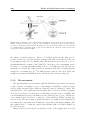
Figure 2.12: Huygenian ocular. The system consists of two conjugated lenses, one has a much
shorter focal distance than the other (f1 > f2 ). a) A collimated beam is focused by the first lens
into the focal point of the second lens, therefore producing a collimated beam of small size. b) If
the incoming beam is slightly convergent (divergent), the first lens focuses it further from (closer
to) the second lens, which due to its short focal distance produces a highly convergent (divergent)
beam.
and pinhole can be adjusted with micrometer precision in x, y, and z directions.
The adjustment should be done in sequential order. Then, by means of mirrors, (if
necessary polarizing) beam splitters, or dichroic mirrors, the reflected beam can be
directed to the combination of detectors (APD, PMT, spectrograph) required by the
experiment.
Alignment of the avalanche photo diode
The reflected beam should be focused into the small active area of the APD with
an (100 mm focal length) achromatic lens. For this purpose, the APD is mounted on
an xyz stage with micrometer precision. The first alignment can be accomplished
by eye but fine adjustments can only be done when a real (fluorescent or scattering)
sample is measured by optimizing the APD position in order to maximize the signal.
Alignment of the photomultiplier tube
Due to the big active area of the PMT, the alignment is considerably simple.
The reflected beam should be focused onto the active area of the PMT with an
achromatic (100 mm focal length) lens. This can be accomplished by eye and no
further adjustments are needed.
Illumination of the active area of the PMT with high intensities (even when it is
switched off) can increase the dark-count rate of the PMT. Eventually, it can take
several days until the nominal dark-count rate is recovered. For this reason, the
active area of the PMT should be covered during the alignment procedure.
28
The fluorescence and light scattering confocal microscope
Alignment of the spectrograph
The collimated reflected beam should be directed first to the VPH grating. Light
dispersed by the grating is collected by the photo objective and focused on the CCD
sensor. Both the photo objective and the CCD sensor should be centered in the
spectral range of interest. The latter can be accomplished with the help of two
different laser light sources, for example the 460 nm line of the Ar-ion laser and the
633 nm of the HeNe laser, as shown schematically in figure 2.13.
Figure 2.13: Alignment of the spectrograph. Both the photo objective and the CCD camera can
be moved in x, y and z directions, as well as tilted in φ and θ. Using a two-color beam helps to
center the photo objective in the spectral range of interest, and to place the CCD camera in the
right position.
The photo objective and the CCD camera can be moved and tilted in all directions. To maximize the detectable spectral range the photo objective needs to be
as close as possible to the grating, and its diaphragm has to be completely open.
Then, the position of the camera and the focus of the photo objective need to be
adjusted in order to produce a sharp image of the spectra in the desired position
of the CCD sensor. For this, it is convenient to use white light illumination and
set the camera on live mode [24] because this allows to monitor on-line how light
of different wavelengths is focused on the CCD sensor. The light dispersed by the
VPH grating should be focused by the photo objective to a straight line on the CCD
sensor. It is advisable to accommodate the camera position in such a way that the
light is focused on a horizontal pixel line of the CCD sensor because in that case the
data analysis is simpler.
Alignment of the detection for light scattering measurements
In this case, annular illumination is used and the diameter of the detected beam
should be reduced with a diaphragm in order to block the reflected light (see figure 2.8). Because of the annular illumination, the reflected light beam used for the
2.4 Operation
29
alignment looks like an annulus. The diaphragm should be placed centered to this
annulus and closed to a point in which no light can pass through. The size of the
diaphragm can be at first adjusted by eye. Once a scattering sample is placed on
the microscope, the size of the diaphragm can be optimized in order to get the best
signal to background.
2.4
Operation
In this section, instructions about how to perform the basic operations with the
microscope are given. First, it is explained what the sample requirements are and
how the sample should be mounted. Second, all the operations related to imaging
are explained. Finally, the instructions to perform time correlated measurements
and to record spectra are given.
Figure 2.14: Control panel of the PC user interface used to operate the home-built confocal
microscope.
Many of the computer controlled functions of the microscope explained below
can be managed from the PC user interface11 . The control panel for this interface
is shown in figure 2.14. For further details about the microscope control and data
acquisition software please refer to appendix A.3.
Before performing any operation from the PC user interface software, it is necessary to boot the local processor of the AD/DA converter by pressing the button
called Boot in the ADWin division of the control panel. This action, in addition to
resetting the local processor of the AD/DA converter, clears up the local memory
of the AD/DA converter and loads all necessary routines.
11
The PC-user interface file is called SAC v7.pxp
30
2.4.1
The fluorescence and light scattering confocal microscope
Sample requirements and mounting
Due to the short working distance of the high NA microscope objective, the samples should be prepared on thin microscope coverslips (0.13 - 0.16 mm). The sample
should be placed on the sample holder (see figure 2.15), fixed with the magnetic
film, and then moved with care to the piezoelectric stage. The region of interest of
the sample should be positioned on top of the front lens of the microscope objective,
with sufficient immersion oil between the objective and the sample.
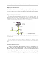
Figure 2.15: Sample holder. The sample holder consists of a thin square plate (∼ 75×75 mm2 )
of steel with a perforation (Ø 20 mm) in the center. The sample should be placed on top of the
sample holder and fixed with a magnetic film. Then, the complete set should be positioned on the
piezoelectric stage.
After placing a new sample on the microscope, the focus should be adjusted.
It is advisable to start by placing the focus of the objective on the glass/air (or
sample/surrounding medium) interface as described in section 2.3.4).
2.4.2
Imaging
The first step to make an image is to mount a sample and to focus the microscope.
Then, from the control panel (figure 2.14) the parameters for scanning an image can
be set: the initial position (Xi and Yi) in µm, the scanning range (Scan Range)
in µm, the number of pixels per line (Pixels), and the counting time per pixel
(Pixeltime) in ms or µs. The process of acquiring an image is initiated by pressing
the button Start, in the division called Surface Scan of the control panel (figure
2.14).
If the Calibration check-box is checked, a calibration procedure is performed before the image scanning in order to account for the delayed response of the piezoelectric stage; i.e. a number of lines is scanned with the set parameters and the corrections parameters, necessary to construct consistent forward- and backward-scanned
images from the collected data, are determined. An overview of this calibration
procedure is given in section 2.2.2. The code of the algorithm used is presented and
commented in the appendix A.3.
2.4 Operation
31
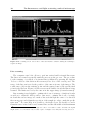
Figure 2.16: Calibration screen. Screen shot of the user interface software during the calibration procedure before the start of the scanning to acquire an image. The software displays the
parameters of the calibration procedure that corrects the effects of the inertia of the piezoelectric
drivers and electronic delays. The curves are the driving signal to scan the x-direction, the capacitive monitor signal of the piezo stage and the actual x-position of the piezoelectric stage after
correction (see section 2.2.2). The thin lines are linear fits used to determine the linear range of
the x-position. Further information can be found in the appendix A.3.
While the test lines for calibration are being scanned, the screen of the user
interface looks like in figure 2.16. The driving and monitor signals of the piezo stage
are displayed together with the corrected x-position (see section 2.2.2)12 .
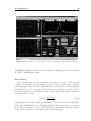
Once the scanning to acquire an image starts, the screen of the user interface
looks like in figure 2.17. On the left, the forward- and backward-scanned images are
displayed and updated line by line as the acquired data is transferred to the PC13 .
In addition, the profile of the last scanned line is also displayed on the upper right
corner of the screen.
12
It is possible that the monitor signal suddenly appears extremely noisy. This is due to instabilities in the monitor output of the amplifier. If this happens, the BNC connector from the
monitor output of the amplifier should be unplugged for some seconds and the scanning should be
restarted.
13
The images displayed on the user interface software are rotated 90◦ counter-clockwise with
respect to the sample, as seen from the front of the microscope.
32
The fluorescence and light scattering confocal microscope
Figure 2.17: Scanning screen. Screen shot of the user interface software during the scanning to
acquire an image.
Line scanning
The computer control also allows to perform vertical and horizontal line scans.
The lines are scanned repeatedly until the user stops the process. The procedure
for the scanning of a vertical or horizontal line is initiated by pressing the buttons
V-Scan or H-Scan of the division Measurement/Line Scan of the control panel. The
range of the line scan is set by the position of the cursors in any of the images. The
round cursor (A) sets the starting point and the squared cursor (B) sets the final
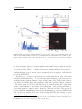
point for the line scan. Figure 2.18 shows a screen shot while a horizontal line is being
scanned. The limits were set by the cursors in the upper image (forward-scanned).
Line scanning is very helpful to optimize the focus of an image of single molecules
as well as to adjust the APD position. One way to optimize the focus of a single
molecule fluorescence image is to make a line scan through the center of a detected
fluorescence spot and adjust the z-position of the sample in order to make the profile
narrowest14 . For extra help, it is possible to check the Gauss Fit check-box, and a
Gaussian curve is fitted after every scanned line and the full width at half maximum
14
Care should be taken to scan through the center of a feature because otherwise the signal
might seem to become narrow only because a part of a higher order Airy disc is being detected.
2.4 Operation
33
Figure 2.18: Line scan screen. Screen shot of the user interface software during a line scan.
(FWHM) is displayed. A line scan is also useful to adjust the position of the APD
in order to maximize the signal.
Data format
The obtained data is stored in the form of a third order tensor. The rows and
columns are determined by the number of pixels of the complete image (forward
and backward). Then, each layer (third dimension of the data tensor) has different
information stored for every pixel. The first and second layers store the x and y
position, respectively, of each pixel in units of the AD/DA digits (AD), which can
be translated into µm by:
X[µm] =
80 X[AD]
32768
(2.4)
The third layer stores the counts (i.e. the number of photons detected in the pixel).
The fourth and fifth layers store the initial and final time, respectively, of each pixel
in ns, with a resolution of 25 ns. The sixth layer contains the capacitive monitor
signal for the x-position of each pixel, again in AD/DA digits.
34
The fluorescence and light scattering confocal microscope
Saving Data
To save the complete data, the buttons Save Data in the division Save Data
of the control panel should be used. The data is saved in Igor binary format [25]
together with the adjacent information entered in the other fields of the Save Data
division of the control panel (Comments, Wavelength, Power, etc.). In addition, the
scanning parameters (Pixeltime, Xi, Yi, Scan Range, Pixels) are stored, as well as
the necessary information to reconstruct the forward and backward images from the
data15 . Software to extract the information from this type of data was programmed
as well but it is not discussed in this dissertation16 .
2.4.3
Time correlated measurements
Two kinds of time correlated measurements are described in this section. Lifetime imaging and fluorescence vs. time traces. Both are performed with the help of
the TCSPC module (see 2.2.3). Details about the operation of the TCSPC module
can be found in its user manual [19]. In these kinds of measurement, data needs to
be collected simultaneously by the AD/DA converter and the TCSPC unit. Therefore, it is necessary to divide the detector signal (simply by a BNC T-connector),
and send it to both the AD/DA converter and TCSPC unit (see sections 2.2.3 and
2.2.4 for the input signal requirements of the AD/DA and TCSPC).
Lifetime imaging
Lifetime imaging consists of recording a fluorescence image in which also the
fluorescence excited state lifetime is stored. That means that each pixel of the image
should contain information about the position, the number of photons counted at
that position, and the time after the excitation pulse at which those photons were
detected (mic-t in section 2.2.4).
Once an interesting region of the sample has been identified, the TCSPC module
should be started first in mode FIFO. Then, the confocal image scanning should
begin, so that in both the TCSPC and confocal data the complete information is
stored. In this manner, every photon seen by the detector is doubly detected, by the
AD/DA counter and the TCSPC, and two sets of data are obtained. The data from
the confocal image, recorded in Igor as described above, contains for every pixel,
besides the position, the time at which the counter was started and the time at
which it was stopped (with 25 ns resolution). The data obtained with the TCSPC
consists of two values for every detected photon, recorded in chronological order:
15
All this information is saved together with the data in the Igor binary file as the note associated
to the saved wave, and one can get access to it with the Igor command note(wavename).
16
The file is called ConfocalAnalyis.pxp and is attached in a CD-ROM to the copy of this
dissertation at the MPI-P library.
2.4 Operation
35
Figure 2.19: Fluorescence lifetime imaging. a) To produce a fluorescence lifetime image, the
confocal data and the TCSPC data need to be linearized in time and synchronized. b) Fluorescence
lifetime image constructed from the data shown in a). c) Fluorescence decay curves of a single
fluorescent dye and of the background are shown for comparison.
the detection time after the excitation pulse mic-t, with 12 ps resolution, and the
detection time from the beginning of the measurement mac-t, with 50 ns resolution
(see section 2.2.4). Then, to obtain a fluorescence lifetime image, it is necessary to
combine these two sets of data in order to assign a position (a pixel) to each detected
photon in the TCSPC.
Another piece of software was developed to synchronize the two sets of data and
construct the lifetime image. To perform the synchronization, both data sets are
linearized in time with an arbitrary origin. A histogram of the TCSPC mac-t data is
done with a bin width equal to the pixel time of the confocal data and then compared
to the latter (figure 2.19.a). If both data sets do not match in time, the origin of the
TCSPC data is shifted to later times (and a small part of the TCSPC discarded17 ),
a new histogram is computed and compared to the confocal data. The process is
repeated until an optimum match is achieved (Figure 2.19.a). Once the TCSPC and
confocal data are synchronized, the detection time (TCSPC mac-t time) of every
TCSPC-detected photon is compared to the initial and final collection times of each
17
Recall that the TCSPC module is started before the confocal image, therefore the first part of
the TCSPC data does not correspond to the confocal data.
36
The fluorescence and light scattering confocal microscope
pixel of the confocal image, in order to find the pixel to which the photon corresponds. At the end, an image is constructed in which for every photon of each pixel
the TCSPC mic-t time is known; i.e. a fluorescence lifetime image. Then, as shown
in figures 2.19.b and 2.19.c, from the fluorescence lifetime image, the fluorescence
excited state lifetime of different molecules or regions of the sample can be studied.
Fluorescence vs. time measurements
Fluorescence vs. time measurements, also called kinetic traces, consist of recording the fluorescence emission of a certain molecule or region of the sample as a
function of time. The procedure to carry out a fluorescence vs. time measurement
is as follows. First, an image of the region of interest of the sample is acquired and
the TCSPC must be ready to start in FIFO mode (see [19] for details). Next, the
round (A) cursor, on any of the confocal images, is positioned on the point of the
sample that is going to be studied. Then, pressing the Start button in the Kinetic
division of the control panel moves the sample to the position marked by the cursor
A18 , opens the shutter of the excitation light, starts recording the photons detected
by the AD/DA counter as a function of time, and displays the kinetic trace on the
top-right graph. Figure 2.20 shows a screen shot of the PC user interface during a
fluorescence vs. time measurement of the feature marked by the cursor A on the
bottom-left (backward) image.
The stage needs around 10 seconds to move to the selected position and reach
stability. This time can be used to start the TCSPC module in FIFO mode to
record the kinetic trace. If this time is not sufficient, the TCSPC module can also
be started earlier. Like this, the fluorescence vs. time trace is recorded independently by the AD/DA counter and the TCSPC unit. However, these two data sets
are different. The data collected by the AD/DA counter and displayed on the PC
user interface is intrinsically binned; i.e. it is not the detection time of each photon
what is recorded, but the number of photons detected within a time interval of a
size determined by the Pixel time parameter in the Kinetic division of the control
panel. This is not convenient because the interesting time scale of the processes involved in the fluorescence fluctuations need to be known a priori in order to choose
the appropriate bin width. In addition, the data presents gaps due to the fact that
the AD/DA card cannot store and deliver data at the same time. So the photons
detected during the time necessary to transfer the data to the computer memory
are not recorded. The Time parameter in the Kinetic division of the control panel
determines how often this data transfer is performed. In contrast, the TCSPC data
is not inherently binned because the TCSPC unit records the detection time of each
photon. The data employed for further analysis is therefore the TCSPC one. The
18
The sample is moved to the position marked by the cursor A in the last active image (also
called top image because the operating system Windows places the last active window on top of
the others).
2.4 Operation
37
Figure 2.20: Kinetic trace screen. Screen shot of the user interface software during the recording
of a fluorescence vs. time trace. The software records the data and updates the display periodically
at a frequency defined by the Time parameter in the Kinetic division of the control panel.
data recorded for the PC user interface is discarded after each measurement but is
of practical importance because it allows to visualize on-line the kinetic trace.
2.4.4
Spectra measurements
The procedure to measure the spectrum of light from a specific point of the
sample is basically the same as that to measure a kinetic traces. Once a feature of
interest is identified in a confocal image, its position should be marked with the round
(A) cursor and the Start button of the Kinetic division of the control panel should
be pressed. The sample is then moved to the desired position, the shutter of the
excitation light is opened and data is collected as explained in the previous section.
However, in this case, the detected light should be directed to the VPH grating
either by a mirror or a beam splitter, depending on the experimental requirements.
The detected light is spectrally dispersed by the grating and detected by the CCD
camera, which has its own control and data acquisition software provided by the
manufacturer [22]. The images acquired with the CCD camera contain the spectral
38
The fluorescence and light scattering confocal microscope
information and can be analyzed with another home made software which is not
discussed in this text19 .
If the VPH grating and the CCD camera are properly aligned and focused (see
section 2.3.4), the spectral response is linear through the whole range of the grating.
After every realignment of the instrument, it is necessary to check the calibration
of the spectrograph. This can be accomplished simply by directing monochromatic
light of different wavelengths to the spectrograph, measuring the position of those
wavelengths on the CCD sensor and obtaining a calibration curve. After a sample
change or small alignment corrections, it is recommended to verify the calibration
curve with one wavelength. This can be easily done by measuring the position of
one laser line on the CCD sensor.
19
The file is called CCDAnalysis.pxp and is attached in a CD-ROM to the copy of this dissertation
in the MPI-P library.
Chapter 3
Modelling the fluorescence signal
of a single molecule through a
layered system
A theoretical method is set-up to model the scanning confocal microscopy fluorescence signal of single molecules through a general (non-magnetic) layered system.
The method considers the fluorescent dye molecule as a point oscillating dipole of
fixed orientation interacting classically with the electromagnetic field. First in this
chapter, the problem is described and the relevant parameters are introduced. Then,
expressions for the de-excitation rates and for the spatial distribution of the excitation field and are derived for single molecules of arbitrary orientation. Finally,
the results obtained for the excitation and the emission are combined to give an
expression for the single molecule fluorescence signal.
3.1
Description of the problem.
The fluorescence signal of a single molecule positioned at the first interface of a
layered system is to be modelled. Excitation and detection of fluorescence is considered to be accomplished with the high numerical aperture microscope objective of
an episcopic illumination scanning confocal optical microscope as the one described
in chapter 2.
The detectable fluorescence intensity emitted by a single molecule, in the absence
of triplet blinking1 , is given by:
ISM = Γexc η
Γr
Γr + Γnr
(3.1)
where Γexc is the fluorescence excitation rate, Γr and Γnr are, respectively, the total
1
The concept of triplet blinking is explained in section 5.1
40
Single molecule fluorescence through a layered system
radiative and non-radiative de-excitation rates of the molecule, and η is the overall
detection efficiency including the collection efficiency of the optical system and the
Γr
quantum efficiency of the detectors. The ratio Γr +Γ
represents the radiative, thus
nr
detectable, fraction of the de-excitation.
It is important to note that for the problem considered here Γnr has two different
components. First, every fluorophore has an intrinsic non-radiative de-excitation
i
rate Γnr
due to the internal relaxation pathways of the molecule which might depend
on experimental conditions such as the surrounding medium (for example solvent
and pH) and the temperature. Second, the nearby layered system can introduce
additional non-radiative decay channels such as excitation of evanescent modes or
direct energy transfer. This leads to an electromagnetic non-radiative de-excitation
em
rate Γnr
. With these considerations equation 3.1 writes:
ISM = Γexc η
Γr
i + Γ em
Γr + Γnr
nr
(3.2)
The intrinsic non-radiative decay rate does not depend on the interactions of the
fluorophore with the electromagnetic field. Therefore, the model presented here
can only account for it by introducing an intrinsic fluorescence quantum efficiency
as an additional parameter. The electromagnetic non-radiative decay rate can be
calculated with the model as presented in the next section.
Accurate determination of η is difficult and can even depend on the alignment of
the detection system. For this reason, the method presented here is set-up for the
calculation of a theoretical single molecule fluorescence signal proportional to the
experimental one.
The influence of the environment on the fluorescence behavior of a molecule can
be theoretically studied in different ways. In the approach presented in this chapter,
the molecule is considered as a point oscillating dipole defined by its transition
dipole moment µ. It is thought to be placed in either side of one of the outer
interfaces of a plane (non-magnetic) layered system and interacting classically with
the electromagnetic field. Figure 3.1 depicts the situation and introduces some of
the coordinates relevant for the calculations.
The present chapter is dedicated to derive expressions for the rates Γexc , Γr and
Γnr of equation 3.1 that permit the calculation of a theoretical single molecule fluorescence signal. Expressions for the electromagnetic de-excitation rates Γr and Γnr
are derived in section 3.2. The excitation rate Γexc is considered in section 3.3.
Interface boundary conditions
The model presented here considers a fluorophore in the outermost interface of
a plane, non magnetic (unitary permeability), layered system. Depending on the
3.2 The emission
41
Figure 3.1: Coordinate system. The orientation of the transition dipole µ of the fluorescent
dye-molecules is defined by β and φ. The direction of the incident or emitted radiation of
wavevector k is defined by ψ and θ.
dielectric contrast, the results on either side of the interface can be very different
due to the electromagnetic boundary conditions for the electric field. For a plane
interface between media A and B, those boundary conditions write:
Ek,A = Ek,B
(3.3)
A E⊥,A = B E⊥,B ,
where A and B are the dielectric constants of the respective mediums. The symbols
k and ⊥ stand for the components of the electric field parallel and perpendicular to
the interface plane.
3.2
The emission
The influence of the surroundings, particularly a nearby conducting surface, on
the spontaneous emission of an oscillating point dipole was first discussed by Sommerfeld [26] and later extended by Chance et al. [27]. Analytical solutions to this
problem have been obtained by introducing the Hertz vector potential or dyadic
Green’s functions [27]. In this chapter, an alternative approach, originally due to
Weyl [28] and used by a number of authors [29, 30], is generalized to be applied to
any non-magnetic layered system. The dipolar field is considered as a superposition of s- and p-polarized plane waves, and the influence of the layered system is
described by its plane-wave reflection coefficients.
It is convenient to normalize all the rates to the total emission of a free dipole
in a given homogenous reference medium:
ΓR =
µ2 ωkR
12π0 R
(3.4)
42
Single molecule fluorescence through a layered system
because the normalized rates do not depend on the actual value of the transition
dipole moment. ω is the frequency and kR is the wavevector (in the reference medium
of refractive index nR ) of the emitted radiation. 0 and R are the dielectric constants
of vacuum and the reference medium respectively.
First, the radiative de-excitation rates to different regions of the space are calculated via the application of the Lorentz reciprocity theorem. Then, following the
back-reacted field approach, the total electromagnetic de-excitation rate is calculated.
3.2.1
Radiative decay rate to different regions of space
By application of the Lorentz reciprocity theorem [31, 32], the radiation emitted
by an oscillating dipole in a certain direction can be calculated as the local electric
field, at the dipole position, generated by a plane wave incident from that direction.
Therefore, the calculation of the radiative decay rate to a given region of space is
analogous to the determination of the electric field intensity generated at the dipole
position by plane waves incident from all possible directions in the region of interest.
The electric field produced by a plane wave in any point of a layered system
can be calculated by solving Maxwell’s equations via a transfer matrix algorithm
(TMA) [33]. In the TMA, the layers (see figure 3.2) are defined by their thicknesses
(di ) and complex dielectric constants (i ). The uppermost and lowermost layers (d0
and dN ) are considered to be semi-infinite and all the interfaces are assumed to be
plane and parallel. The total thickness of the layered system is assumed to be small
in comparison to the size of the incident plane wave front.
A plane electromagnetic wave defined by its wavevector k, the parallel (to the
incidence plane) component of its electric field E p , and the perpendicular component
E s , is considered to strike one of the outermost interfaces with an angle of incidence
θ0 . The angle of incidence (θ0 ) determines the component of the wavevector parallel
to the interfaces, kρ , which due to the electromagnetic boundary conditions, remains
constant through the whole multi-layer system. The electric field (amplitude and
phase) in a given z-position of the layered system, which can be thought as the
interference result of the waves successively reflected and refracted at the interfaces,
can be calculated via the TMA as a function of kρ or equivalently as a function of
θi (= arcsin kρ /ki ).
By considering the symmetry of the dipole field in front of a plane interface, it is
found that the emission rate of a molecule with an arbitrary out of plane orientation
Γ(φ) (see figure 3.1), can be calculated from the emission rates of the two limiting
cases of dipoles parallel Γk and perpendicular Γ⊥ to the interface [34]2 :
Γ(φ) = sin2 (φ) Γk + cos2 (φ) Γ⊥
2
Equation 3.5 is valid after 2π-integration over the azimuth angle (β in figure 3.1).
(3.5)
3.2 The emission
43
Figure 3.2: General multi-layer
system showing the relevant parameters for the transfer matrix algorithm (TMA) and the coordinate
system.
It is therefore sufficient to calculate the two particular cases.
After the introduction of the normalization factors (equation 3.4) and 2π-integration
around the azimuthal angle, the emission rates to a region of space in medium m
for a parallel and perpendicular dipole can be calculated by the following integrals:
Γm,k
3 k0
=
4 nR
kZmax
kρ
(|Ex (kρ )|2 + |Ey (kρ )|2 ) dkρ
km − kρ
p
0
(3.6)
Γm,⊥
3 k0
=
2 nR
kZmax
kρ
|Ez (kρ )|2 dkρ
km − kρ
p
0
where k0 (= 2π/λ) and km (= nm k0 ) are the wave vectors of the emitted radiation
in vacuum and in medium m, respectively. nR is the refractive index of the reference
medium; i.e. the rates are normalized to the total emission of a dipole in a medium
of refractive index nR . Ei (kρ ) are expressions for the Cartesian components of the
electric field at the dipole position as a function of kρ . They are obtained via the
TMA for plane waves incident from medium m and depend on the thicknesses and
dielectric constants of the layers and the wavelength of the emitted radiation.
The integration limits define the region of space of interest. To compute the
far-field emission to a complete semi-space, the integration should be accomplished
between zero and the wavevector of the emitted radiation in medium m (kmax = km ).
Further integration between km and infinity accounts for the contribution of high
wavevector, evanescent components of the dipole field, which can eventually propagate as waveguide modes in some of the layers but do not contribute to the detectable
44
Single molecule fluorescence through a layered system
far field emission. Taking into account that kρ = km sin θm , it is possible to calculate
the emission rate in a given angular range by integrating between the appropriate
limits of kρ . To calculate the theoretical fluorescence signal, the radiation emitted
into the collection solid angle of the microscope objective needs to be computed.
3.2.2
Total electromagnetic decay rate
The normalized total electromagnetic decay rate for a dipole with dipole moment
µ, located in a reference medium of dielectric constant R and in front of a plane
layered system, can be calculated by application of Poynting’s Theorem as follows
[30, 34]:
em
Γtotal
=1+
6π0 R
Im[Ebr · µ∗ ]
µ2 k3R
(3.7)
where 0 is the permittivity of vacuum, R is the dielectric constant of reference
medium, and kR is the wavevector of the emitted radiation in the reference medium.
Ebr is the back-reacted electric field, which is defined as the difference, at the dipole
position, between the field in the presence of the interface and the field in the free
dielectric reference medium. A detailed description of the calculation of Ebr can be
found in [34, 35].
In the case of a plane interface, due to symmetry reasons, the parallel (to the
interface) component of the back reacted field generated by a perpendicular dipole
vanishes, and viceversa. Therefore, the total back-reacted field generated by a dipole
of arbitrary orientation can be written as a composition of the back-reacted fields
generated by the parallel and perpendicular components of the dipole (Ebrk and Ebr⊥
respectively):
Ebrk sin φ cos β
Ebr = Ebrk sin φ sin β
Ebr⊥ cos φ
(3.8)
where φ and β are the azimuth and polar angles that define an arbitrary direction
for the transition dipole as shown in figure 3.1. Then, the product Ebr · µ∗ for a
dipole with arbitrary orientation writes:
Ebrk sin φ cos β
sin φ cos β
Ebr · µ∗ = Ebrk sin φ sin β · µ∗ sin φ sin β
Ebr⊥ cos φ
cos φ
= µ∗ (sin2 (φ) Ebrk + cos2 (φ) Ebr⊥ )
(3.9)
The back reacted fields generated by a parallel and a perpendicular dipole can
3.2 The emission
45
be calculated by the following integrals [34]:
Ebrk
iµ
=
4π0 R
Z∞ kρ kR,z rP (kρ )
kρ k2R rS (kρ )
−
+
dkρ
2
2 kR,z
0
(3.10)
Ebr⊥ =
iµ
4π0 R
Z∞
(kρ )3
rP (kρ ) dkρ
kR,z
0
where kR is the wave vector of the emitted radiation in the reference medium, and
kR,z its projection on the z-direction. rP and rS are the reflectivity coefficients of
the layered system (from the reference medium), for a p- and s-polarized plane wave,
respectively. They are functions of kρ and can be calculated with the TMA. Then,
the term in brackets in equation 3.7 does not depend on µ, and the normalized
total electromagnetic decay rates for the parallel and perpendicular dipoles can be
calculated as:
∞
Z 2
3
kρ kR rS (kρ )
kρ kR,z rP (kρ )
em
Γtotal,k
= 1+
Im i
+
−
dkρ
3
2 kR
2
2 kR,z
0
(3.11)
em
Γtotal,⊥
= 1+
3
Im i
2 k3R
Z∞
(kρ )3
rP (kρ ) dkρ
kR,z
0
Finally, from equations 3.7 and 3.9, the total electromagnetic decay rate of a
molecule with and arbitrary out-of-plane orientation φ is calculated as:
em
em
em
Γtotal
(φ) = sin2 (φ) Γtotal,k
+ cos2 (φ) Γtotal,⊥
(3.12)
The case of a dipole on the inner side of the first interface
So far, the total electromagnetic decay rate was calculated for a dipole in front of
the layered system. It is simple to extend this result to the case of a dipole infinitely
close to the interface from the inner side of the first layer. Due to the fact that
the materials are non-magnetic, the only change to the Poynting computation of
the power flux arises from the discontinuity of the perpendicular component of the
em
electric field. Then, Γtotal,k
takes the same value on both sides of the interface and
em
Γtotal,⊥ needs to be scaled by a factor (R /1 )2 , where 1 is the dielectric constant of
the first layer.
46
3.2.3
Single molecule fluorescence through a layered system
Non-radiative electromagnetic de-excitation rate
em
The non-radiative electromagnetic decay rate Γnr
can be calculated as the difem
and the total radiative
ference of the total electromagnetic de-excitation rate Γtotal
decay rates to the complete space. According to figure 3.2:
em
em
Γnr
(φ) = Γtotal
(φ) − Γ0 (φ) − ΓN (φ)
(3.13)
where Γ0 and ΓN are the radiative decay rates to the semi-spaces above and below
the thin layered system.
3.2.4
Detectable fraction of the de-excitation rate
The detectable fraction of the de-excitation rate is the fraction corresponding
to radiation emitted into the collection solid angle of the objective. For an ideal
i
fluorophore with a Γnr
= 0 and a transition dipole with an out-of-plane orientation
according to φ, this fraction writes:
Γdet (φ) =
sin2 (φ) Γobj,k + cos2 (φ) Γobj,⊥
Γobj (φ)
=
em
em
em
Γtotal
(φ)
sin2 (φ) Γtotal,k
+ cos2 (φ) Γtotal,⊥
(3.14)
Γobj is the radiative de-excitation rate emitted into the collection solid angle of
the microscope objective calculated by the integrals 3.6 between the appropriate
em
limits. Γtotal
is the total de-excitation rate calculated by equations 3.11. Both Γobj
em
and Γtotal are normalized to the total emission of a dipole in the same reference
medium.
i
6= 0
Modifications for the case of a fluorophore with Γnr
The intrinsic quantum efficiency QE of a fluorophore in a given medium is defined
as a function of its intrinsic radiative and non radiative de-excitation rates in that
medium:
QE =
Γri
i
Γri + Γnr
(3.15)
i
So far, an ideal fluorophore with Γnr
= 0, or equivalently with QE = 1, was
i
considered. If a fluorophore has Γnr
6= 0, its quantum efficiency is smaller than 1,
and the amount of radiation emitted in a time unit is reduced.
Γdet is composed of rates which are normalized to the total emission of a free
dipole in a reference medium (Γri ). Therefore, in order to account for a QE < 1,
an intrinsic non-radiative decay rate, normalized as well to the total radiative deem
excitation rate, needs to be added to Γtotal
in the denominator of Γdet (as shown in
3.3 The excitation
47
equation 3.2). It is easy to express this intrinsic normalized non-radiative decay rate
i as a function of the QE:
Γnr
i =
Γnr
i
Γnr
1 − QE
=
i
Γr
QE
(3.16)
i is a function exclusively of QE and is therefore not expected to depend on
Γnr
external parameters such as the properties of the layered system or the position and
orientation of the fluorophore with respect to the interfaces. Then, the detectable
i
6= 0
fraction of the emitted radiation for an arbitrarily oriented fluorophore with Γnr
writes:
sin2 (φ) Γobj,k + cos2 (φ) Γobj,⊥
Γobj (φ)
Γdet (φ) = em
=
em
em
i
+ 1−QE
+ cos2 (φ) Γtotal,⊥
sin2 (φ) Γtotal,k
Γtotal (φ) + Γnr
QE
3.3
(3.17)
The excitation
Far from saturation, the excitation rate of a fluorophore positioned at r and
with a transition dipole moment µ, is proportional to the square modulus of the
projection of the electric field at that position E(r) along the dipole direction:
Γexc (r) ∝ |µ · E(r)|2
(3.18)
As a consequence, in scanning confocal optical microscopy (SCOM), the spatial distribution of the fluorescence signal of a single molecule reflects the spatial
distribution of the electric field intensity along the direction of the molecule transition dipole. In the experimental conditions, this electric field is produced by the
excitation light when it is focused by the microscope objective through the layered
system of the samples. In this section, a theoretical method to calculate this field is
presented.
3.3.1
Electric field distribution near a geometric focus in a
layered system
The time independent part of the electric field E in a point r near the geometric focus of an aplanatic optical system, such as the microscope objective, can be
calculated by adding the contributions of an angular distribution of electromagnetic
48
Single molecule fluorescence through a layered system
plane waves traveling to the focus as [36]:
ZZ
f E0 eik·r dΩ
E(r) = C
(3.19)
Ω
where C is a constant, E0 is the complex amplitude of the plane waves at an origin
(normally the Gaussian focal point) from which the position of the point of interest
r is measured, k is the wavevector of the radiation, and Ω is the solid angle defining the angular distribution of plane waves. f is a scalar function called strength
function, it depends on the properties of the focusing system and accounts for the
different intensities of rays focused in different directions. Equation 3.19 is valid
for an aberration free optical system and under geometric optics approximation; i.e.
the distance between the exit pupil plane and the image region (df in figure 3.3),
and the linear dimensions of the exit pupil (front lens of the microscope objective),
are assumed to be large in comparison to the wavelength. This approach was first
proposed by Richards and Wolf [36, 37] and used by a number of authors to tailor
the focus geometry [38] or to determine the three-dimensional orientation of single
molecules [39, 40]. Those works considered the focus of light to occur through an
homogeneous medium or in the presence of a single interface. In contrast, in the
model presented here, the focusing of light occurs through a layered system. The
mentioned approach needs therefore to be generalized to consider the focusing of a
plane wave front through a multilayer system.
The next paragraphs are dedicated to the calculation of the electric field at the
Gaussian focus E0 , the product k·r, and the introduction of the strength function f ,
in order to write the integral 3.19 for the focusing of light through a layered system.
Figure 3.3 shows the geometry of the problem and introduces some of the variables
and the coordinates used in the following calculations.
A monochromatic, linearly polarized plane-wave front is considered as the source
field Esrc which is focused through a layered system with a microscope objective. In
order to account for the amplitude of the plane waves at the focus (E0 ), it is first
necessary to find an expression for the electric field generated by a focused wave in
any point of the layered system. A Cartesian coordinate system is considered with
the x-axis along the polarization direction of Esrc and the z-axis along the optical
axis, as shown in figure 3.3.a. For simplicity, a source field with unitary intensity is
considered: Esrc = (1; 0; 0).
Plane waves that are focused by a certain point of the rear lens of the objective,
strike the layered system with a given incidence angle and defined p- and s-polarized
components (see figure 3.3). The radial position of the focusing point R defines the
incidence angle θ of the focused wave as explained in section 2.2.1. The angular
position of the focusing point ψ defines the p- and s-polarized components of the
focused wave.
The local electric field in any point of the layered system, produced by a plane
3.3 The excitation
49
Figure 3.3: Electric field near a geometric focus. a) Geometry of the problem of the calculation of
the electric field near a geometric focus. The source field (Esrc ) is a linearly polarized, monochromatic plane wave front (k = 2π/λ). A Cartesian coordinate system is taken such that the source
field lies along the x axis, and the optical axis along the z direction. Focusing is accomplished by
an aplanatic system. Rays focused at different radial positions R of the focusing lens are focused
with a different angle θ. b) Rays focused at different angular positions of the lens (ψ) are focused
s
p
respectively).
and Esrc
with different p- and s- polarized components (Esrc
wave incident with angle θ with respect to z and with given p- and s-components
of its electric field, can be calculated with the transfer matrix algorithm (TMA, see
section 3.2). The TMA calculates the fields in a primed coordinate system rotated
around the z-axis in order to place the y’-axis along the s-polarized component,
as shown in figure 3.3.b (and 3.2). In this rotated coordinate system, the p- and
s-polarized components of the source field are:
p
Esrc
= cos ψ
s
Esrc
= − sin ψ
(3.20)
It is convenient first to use the TMA to obtain expressions for the electric field
components at the point of interest generated by an incident plane wave with both
p- and s-components of unitary intensity. Let those field components in the rotated
coordinate system be Ezp0 , Exp0 , and Eys0 . For a given wavelength, the expressions of
these normalized field components are a function exclusively of the layered system
properties (thickness di and dielectric constant i of each layer, and the z-position
in the layered system zls ) and the angle of incidence θ:
Exp0 = Exp0 (θ, di , i , zls )
Eys0 = Eys0 (θ, di , i , zls )
(3.21)
Ezp0 = Ezp0 (θ, di , i , zls )
A wave of Esrc focused by a given point of the rear lens at an angular position
defined by ψ, has a p- and an s-polarized components given by equations 3.20. Then,
to obtain the components of the electric field at the point of interest generated by
50
Single molecule fluorescence through a layered system
a such a wave, it is necessary to multiply the normalized expressions 3.21 by the
corresponding p- or s-component of the source wave:
p
Exp0 (θ, di , i , zls )Esrc
Exp0 (θ, di , i , zls ) cos ψ
E0 x0
s
s
s
E00 =
E0 y0 = −Ey0 (θ, di , i , zls )Esrc = −Ey0 (θ, di , i , zls ) sin ψ (3.22)
p
Ezp0 (θ, di , i , zls ) cos ψ
E0 z0
Ezp0 (θ, di , i , zls )Esrc
This is the electric field, written in the primed coordinates system, generated at
the point of interest of the layered system by a source plane wave focused by a point
of the rear lens of the objective defined by ψ and θ3 . Thus, in order to obtain E0 ,
E00 has to be rotated to the original xyz coordinates system:
E0 x0 cos ψ − E0 y0 sin ψ
cos ψ sin ψ 0
E0 = E00 − sin ψ cos ψ 0 = E0 x0 sin ψ + E0 y0 cos ψ
E0 z0
0
0
1
(3.23)
Finally, the x-, y-, and z-components of E0 can be written as a function of θ and
ψ as:
E0 x = Exp0 (θ) cos2 ψ + Eys0 (θ) sin2 ψ
E0 y = Exp0 (θ) − Eys0 (θ) cos ψ sin ψ
(3.24)
E0 z = Ezp0 (θ) cos ψ
where the dependencies on di , i and zls were not explicitly written.
Next, to calculate the integral 3.19 in an arbitrary point near the geometric focus,
an expression for k · r is necessary. According to figure 3.3, one can write:
ρ cos ϕ
r = ρ sin ϕ
zP
cos ψ sin θ
k = k sin ψ sin θ
cos θ
(3.25)
and the scalar product leads to:
k · r = k(ρ sin θ(cos(ψ − ϕ)) + zP cos θ)
(3.26)
The microscope objective is an aplanatic system of revolution; i.e. axially stigmatic and obeying the sine condition all around the z axis. Hence, the plane wave
front of the source field in the object space is transformed into a spherical wave
front in the image space without aberrations. The strength function f is in this case
3
As shown in section 2.2.1, a point of the objective rear lens can be equivalently defined in polar
coordinates (R, ψ) or by a set (θ, ψ), because R = sin θ Rrl nglass /N A.
3.3 The excitation
51
found to be [37]:
√
f (θ) =
cos θ
(3.27)
Introducing in integral 3.19 the electric field components 3.24, the path difference
exponent 3.26, and the strength function 3.27:
Z2π θZmax√
Ej (r) = C
cos θ E0 j (θ, ψ) eik(ρ sin θ(cos(ψ−ϕ))+zP cos θ) sin θ dθ dψ
(3.28)
0 θmin
where j stands for x, y, or z, and the solid angle Ω is integrated in spherical coordinates. The azimuth angle ψ is integrated all around the z-axis, and the focusing
angle range (θmin and θmax ) depends on parameters such as the NA of the objective,
the diameter of the illumination beam and the blocking disc in annular illumination
(see section 2.2.1).
The integral 3.28 permits the calculation (up to a constant) of the electric field in
any point near the focus of the microscope objective, when the latter is illuminated
with a linearly polarized plane wave front. The electric field distribution over a
region near the focus can be calculated by performing the integration for each point
r of the region. Nevertheless, if the illumination beam has rotational symmetry
around the z-axis, and for points r in a plane parallel to the focal plane, it is only
necessary to calculate one in-plane (xy) component of the electric field along two
directions, and the z-component along one direction. In particular:
Ex (r = (x, 0, zP )) = Ex (ρ, ϕ = 0, zP ) ≡ Exx
π
Ex (r = (0, y, zP )) = Ex (ρ, ϕ = , zP ) ≡ Exy
2
Ez (r = (x, 0, zP )) = Ez (ρ, ϕ = 0, zP ) ≡ Ezx
(3.29)
(3.30)
(3.31)
From these components, the total field along any radial direction, defined by
ϕ = α, in the plane of interest can be calculated. To understand this point, it is
necessary to make some symmetry considerations; first for the in-plane components
Ex and Ey , and then for the Ez component.
Due to the mirror symmetry of the problem with respect to the x-axis, any ycomponent of the fields along the x-axis vanishes. One way to see this, is to imagine
that the waves focused through the positive-y semi-plane of the objective rear lens
generate a non-zero y-component along the x-axis. Then, the plane waves focused
through the negative-y semi-plane would generate a y-component, along the x-axis,
of equal magnitude and opposite sign. Figure 3.4.a shows this effect schematically.
Due to the inversion symmetry with respect to the y-axis imposed by the direction of the source field, any y-component of the fields along the y-axis vanishes. One
way to see this, is to imagine the source field generates a non-zero y-component in a
52
Single molecule fluorescence through a layered system
Figure 3.4: Symmetry considerations in the focal plane. a) Due to the mirror symmetry of the
problem with respect to the x-axis, no y-components of the fields are generated along the x-axis.
b) Due to the inversion symmetry with respect to the y-axis imposed by the source field direction,
no y-components are generated along the y-axis. c) Then, the fields generated along the x- or
y-axis, have only x in-plane component.
given point of the y-axis. Then, as shown in figure 3.4.b, half a period later both the
source field and the generated y-component have the same amplitude and point in
the opposite direction. On the other hand, it is possible to choose an x-axis pointing
in the opposite direction. This would invert the direction of the source field but not
the generated y-component. Then, there are two valid solutions for the generated
y-component produced by the same source field but pointing in opposite directions.
Therefore, the y-component of the electric field along the y-axis needs to be null.
As a consequence, a source field polarized along the x-axis generates in-plane
(z = zP ) fields along the x- and y-axis that only have x-components, as depicted in
figure 3.4.c. To describe the in-plane field distribution it is then sufficient to know
Exx and Exy :
E(r = (x, 0, zP )) = (Exx , 0, Ezx )
Eyx = 0
E(r = (0, y, zP )) = (Exy , 0, Ezy )
Eyy = 0
(3.32)
To obtain the field along an arbitrary in-plane direction α it is convenient to
consider a primed coordinate system rotated an angle α around z, in order to place
the direction of interest along the x’-axis. The source field (Esrc = (1, 0, 0)) can be
decomposed in two components along the rotated axis as shown in figure 3.5.a:
Esrc = Esrc,x0 + Esrc,y0
Esrc,x0 = cos α
(3.33)
Esrc,y0 = − sin α
Taking into account that no field components perpendicular to the source field are
3.3 The excitation
53
generated (equations 3.32), Esrc,x0 and Esrc,y0 generate the fields depicted in figure
3.5.b, which can be calculated by scaling the components Exx and Exy (equations
3.29 and 3.30) with the corresponding components of the source field. Then, the
fields generated along the x’-axis are:
0
Exx0 = Exx Esrc,x0 = Exx cos α
0
Eyx0 = −Exy Esrc,x0 = Exy sin α
(3.34)
Figure 3.5: Electric fields along an arbitrary direction. a) In-plane fields generated by the source
field in a coordinate system x’y’ rotated α around z-axis with respect to the original coordinates
system xy. b) Electric fields generated by the x’- and y’-components of the source field. c) Due
to the inversion symmetry of the z-component of the source field with respect to the z-axis in any
incidence plane, the field generated along the z-axis have zero z-component.
To write the field along the arbitrary in plane direction ϕ = α on the original xy
0
0
coordinates system, the contributions of Exx0 and Eyx0 on the x- and y-axis of the
original coordinates system have to be added4 :
0
0
0
0
Ex (ρ, ϕ = α, zP ) = Exx0 cos α + Eyx0 sin α = Exx cos2 α + Exy sin2 α
Ey (ρ, ϕ = α, zP ) = Exx0 sin α − Eyx0 cos α = (Exx − Exy ) sin α cos α
(3.35)
Next, it necessary to show that Ez is zero both along the y- and z-axis. First,
following the same reasoning that lead to the nullity of Eyx and Eyy , it can be seen
that Ezy has to be zero as well. Second, in a similar way, as depicted in figure 3.5.c,
for any plane of incidence, the p-component of the source field focused through the
one half of the objective lens generates a field along the z-axis opposite to the one
generated by the p-component of the source field focused through the other half of
the objective. Then, Ezz is zero and as a consequence, it is possible to obtain the
4
This is basically the same projection that was done to obtain E0 from E00 in equation 3.23.
54
Single molecule fluorescence through a layered system
projection on any other radial direction by:
Ez (ρ, ϕ = α, zP ) = Ezx cos α
(3.36)
Summarizing, the field in any point (ρ, ϕ) of a plane parallel to the focal plane
(z = zP ) can be calculated by means of the x- and z-components of the electric field
along the x-axis and the x-component along the y-axis (Exx , Ezx and Exy ; equations
3.29, 3.31 and 3.30 respectively) by:
Ex (ρ, ϕ, zP )
Exx (ρ) cos2 ϕ + Exy (ρ) sin2 ϕ
= (E x (ρ) − E y (ρ)) sin ϕ cos ϕ
E(r = (ρ, ϕ, zP )) =
E
(ρ,
ϕ,
z
)
y
P
x
x
x
Ez (ρ, ϕ, zP )
Ez (ρ) cos ϕ
(3.37)
In order to calculate the fluorescence excitation rate of a single molecule, it
is necessary to write an expression for the projection of this electric field on the
direction of the transition dipole of the molecule µ (equation 3.18). If the orientation
of µ is defined by an azimuth angle φ and a polar angle β, as shown in figure 3.1,
the projection of the excitation field on the dipole direction is:
E(r) · µ = Ex (r) sin φ cos β + Ey (r) sin φ sin β + Ez (r) cos φ
(3.38)
Finally, recalling equation 3.18 the fluorescence excitation rate for a molecule
positioned at r, and with a transition dipole oriented according to φ and β is:
Γexc (r, φ, β) ∝ |Ex (r) sin φ cos β + Ey (r) sin φ sin β + Ez (r) cos φ|2
3.4
(3.39)
Single molecule fluorescence signal
At this point, it is possible to recall equation 3.1 and combine the results obtained
for the excitation and the emission in order to write an expression for the theoretical
fluorescence signal of a fluorophore in the outermost interface of a layered system:
theo
ISM
(r, φ, β) = Γexc (r, φ, β) Γdet (φ)
(3.40)
where Γexc is calculated by equation 3.39 and Γdet by equation 3.17.
Because of the uncertainty in the detection efficiency (η in equation 3.1) and
that the electric field in Γexc is calculated up to a constant, this theoretical signal
is proportional to the experimental one. For a given orientation of the transition
3.5 Conclusions
55
dipole of the fluorophore, Γexc defines the spatial distribution of the fluorescence signal intensity and Γdet scales the signals according to the detectable radiation emitted
from a molecule with the given out-of-plane orientation.
3.5
Conclusions
A method to model the fluorescence signal of single molecules was set up by
considering the chromophores as oscillating dipoles interacting classically with the
electromagnetic field, placed at the outer interface of a layered system and with
arbitrary orientations.
The method is of general applicability to any non-magnetic plane layered system
and considers the excitation and the emission separately. Calculations performed
with this model can be useful to design and compare experimental configurations
(i.e. different illumination modes, materials and thicknesses of the layered system
and detection schemes) and to determine the three-dimensional orientation of single
chromophores under different conditions.
Chapter 4
Excitation and detection of single
molecule fluorescence through a
thin gold film
In this chapter, it is demonstrated that fluorescence of single molecules in the
nanometric vicinity of a thin gold film can be detected and studied through the gold
film with an epi-illumination scanning confocal microscope. The influence of the
separation distance to the gold film is experimentally studied, as well as different
illumination modes to discriminate the contributions of transmitted and forbidden1
light for excitation. The theoretical model presented in chapter 3 is applied for the
calculation of theoretical single molecule fluorescence signals in the experimental
conditions. Theoretical and experimental signals are compared in order to interpret
the observations.
4.1
Introduction
A number of processes of great technological and scientific importance involve a
fluorophore working near a metallic layer. Among the most important certainly are
sensitized solar cells, organic light emitting diodes and a variety of sensors.
The problem of spontaneous emission near a conducting surface has been already studied, both experimentally and theoretically, for several decades. The first
theoretical approach to the problem was reported by Sommerfeld in 1909 [26], and
after the pioneering experiments by Drexhage et al. [41–43], a considerable number
of experimental and theoretical investigations were dedicated to study the influence
of a nearby metallic layer on the fluorescence emission [27, 29, 44–47].
More recently, room-temperature optical spectroscopy of single fluorescent molecules
1
By forbidden light it is meant light incident at angles higher than the angle of total internal
reflection.
58
Single molecule fluorescence through a thin gold film
became possible [48,49], and since then, an increasing number of scientific questions
are being addressed on a single molecule level. Surprisingly, only one experimental
work was reported of single molecule fluorescence near a metal surface. Yokota et
al. imaged single fluorescently labelled proteins with a surface plasmon fluorescence
microscopy set-up in 1998 [50]. In those experiments, excitation was accomplished
by the surface plasmon field at the metal/solution interface via a Kretschmann prism
coupling configuration, and fluorescence collection was done with a high numerical
aperture objective from the other side of the sample. The same geometry was later
modelled by Enderlein [51].
Figure 4.1: Experimental configuration. a) The Cartesian coordinate system adopted takes
the polarization direction of the illumination beam as reference for the x-axis and the z-axis is
perpendicular to the interfaces. The orientation of the transition dipoles of the chromophores (µ)
is defined by φ and β. The direction of emitted or incident radiation (of wavevector k) is defined
by θ and ψ. b) High angle of incidence illumination (forbidden light, FL). c) Low angle of incidence
illumination (transmitted light, TL).
The experimental scheme presented here differs from the one of Yokota et al.
A sample scanning confocal microscope was used in an episcopic illumination (epiillumination) arrangement from the gold side (see figure 4.1.a). The fluorescence of
single molecules is excited and detected from the same side of the sample, through
the gold film. In comparison to the experimental scheme of Yokota et al., this scheme
presents two important advantages. First, the sample is not constantly illuminated
because the confocal scanning technique allows to excite and detect fluorescence on
one (diffraction limited) spot of the sample at a time. This considerably reduces
irreversible photo-bleaching of the samples, which is of major importance in single
molecule experiments. Second, the chromophores side of the sample remains free,
therefore allowing the application of a complementary technique. At this point,
it is worth remarking that due to its metallic properties in the visible range, its
chemical stability, and the possibility of obtaining atomically flat terraces, gold has
4.2 Experimental
59
became one of the most widely used substrates for a number of techniques, such as
scanning tunnelling microscopy (STM, [52]), atomic force microscopy (AFM, [53])
and electrochemistry (EC, [54]).
In this chapter, experimental and theoretical investigations are combined to address the following questions. Is it at all possible to detect the fluorescence of single
molecules through a thin metallic film? If that is the case, how close to the gold
film can the molecules be before their emission becomes undetectable? How does
this experimental scheme compare to the detection from the air side and to the case
without the gold film?
4.2
Experimental
The sample geometry is depicted in figure 4.1 together with the illumination
modes employed in the experiments. In this section, details about the sample preparation and the measurement procedures are given.
4.2.1
Sample preparation
The sample preparation consists of five steps: cleaning of the glass substrates,
deposition of the gold film, functionalization of the gold surface, layer by layer
deposition of the polyelectrolyte spacer, and finally deposition of the fluorescent
dye-molecules.
Thin (0.13 − 0.16 mm) glass coverslips (N◦ 1, Menzel-Gläser ) were cleaned successively with Hellmanex 2%, Milli-Q water and ethanol (≥ 98%, Riedel - de Haën).
In addition, to remove any rest of organic material, the coverslips were heated in air
for two hours at 500 ◦ C. Next, a 44 nm gold (Agar Scientific Ltd.) film was thermally
evaporated onto the substrates (thermal evaporator: Edwards FL400 ). The freshly
prepared gold surfaces were functionalized with a self-assembled monolayer (SAM)
of 3-mercaptopropionic acid (MPA, Aldrich) as the substrates were immersed in a
0.03 M Milli-Q water solution of MPA for one hour. After that, the substrates were
thoroughly rinsed with Milli-Q water in order to remove all unbound MPA. The so
prepared surfaces contain free carboxylic groups, which hydrolyze in water to render
the surface negatively charged. The next step is the layer by layer deposition of the
polyelectrolyte spacer which was accomplished based on the procedure published by
Decher [55]. Successive polyelectrolyte layers of positively charged poly(allylamine
hydrochloride) (PAH; MW 70 000, Aldrich), and negatively charged poly(styrene
sulfonate) (PSS; MW 70000, Aldrich) were deposited onto the functionalized gold.
Both polyelectrolytes were deposited from 0.02 monomol/l water solutions. Salts
were added to the solutions to adjust the ionic strength; MnCl2 (99%, Merck ) 0.5 M
was used for the PSS solution and NaBr (99+%, Aldrich) 2 M for the PAH [56].
60
Single molecule fluorescence through a thin gold film
The acidity of both polyelectrolyte solutions was adjusted to pH=2 by adding HCl.
To perform the deposition, the samples were alternatively immersed in the polyelectrolyte solutions for 20 minutes, starting with PAH. In between immersions, the
samples were thoroughly rinsed with water and dried with nitrogen. Samples with 1,
2, 3 and 4 PAH-PSS bilayers were prepared, corresponding to spacer thicknesses of
4.5, 10, 15, 24 nm, respectively, as determined in earlier studies [46, 57]. Before use,
both polyelectrolytes were purified in order to minimize the fluorescence background.
PAH was purified by dialysis with a membrane tube with a cut-off molecular weight
of 3500 (Spectra/por-6, Spectrum Laboratories Inc.). The dialysis was conducted for
six days as the water was exchanged twice a day. PSS was purified by a controlled
precipitation method. The polymer was dissolved in water and then the solution
was transferred slowly (drop by drop) into ethanol (≥ 98%, Riedel - de Haën) close to
its freezing temperature (-50 to -60 ◦ C). The precipitated polymer was then filtered
and dried in vacuum. After this treatment the fluorescence background was reduced
considerably and reached a level low enough to allow for single molecule measurements. Namely, a typical sample with four PAH-PSS bilayers presented between
none and two diffraction limited impurities with fluorescence signals comparable to
the one of a single dye-molecule within an area of 10 × 10 µm2 .
Single fluorescent dye-molecules 1,1’,3,3,3’,3’-hexamethylindicarbocyanine iodide
[DiIC1(5), Molecular probes, maximum excitation at λexc = 638 nm, maximum emission at λem = 670 nm] were deposited electrostatically on a negatively charged surface terminated with PSS, by immersing the samples for one minute in a 10−10 M,
Milli-Q water solution of the dye. Then, the samples were rinsed with Milli-Q water
and dried with a stream of nitrogen.
4.2.2
Measurement
The samples were studied in the SCOM set-up described in chapter 2. Fluorescence of single molecules was excited and detected through the gold film with an
epi-illumination scheme as shown in figure 4.1.a. He-Ne laser light, with a wavelength λ = 633 nm, was used for excitation. The illumination beam was linearly
polarized and the intensities used ranged from 3 to 12 kW/cm2 2 . Suitable dichroic
mirror, Notch and long-pass filters were used to separate fluorescence from reflected
excitation light. Fluorescence micrographs were recorded by scanning the samples
with three different modes of illumination, as depicted in figure 4.1. First, images
were acquired under full beam (FB) illumination. Second, by using a blocking disc,
images were acquired under annular illumination, corresponding to large angles of
incidence; in the following, this scheme is called forbidden light (FL) illumination.
2
These intensity values are not the actual intensities at the focus. They are calculated simply by
dividing the full beam intensity by the area of the focal spot (A) given by the theoretical diffraction
limit: A = πR2 ; R = 0.61 λ/N A). Therefore, they would only represent the actual intensity at the
focus of a transparent non-absorbing sample.
4.2 Experimental
61
Finally, images were also recorded by illuminating with a reduced beam diameter,
corresponding to small angles of incidence; in the following, this scheme is called
transmitted light (TL) illumination.
The range of angles of incidence corresponding to each illumination mode depends on the numerical aperture of the microscope objective (NA= 1.4), the refractive index of the focusing medium (nglass = 1.503), and on the beam and blocking
disc diameter, as explained in section 2.2.1. For FB and FL illumination modes, the
beam diameter was adjusted to completely illuminate the rear lens of the objective,
which has a diameter of 8.9 mm. In the case of TL illumination, the beam diameter
was reduced to 5 mm. The blocking disc used in the FL illumination mode had a
diameter of 5 mm. Then, the ranges of angles of incidence θ corresponding to each
illumination mode are:
- Full beam (FB) illumination: 0◦ < θ < 68.6◦
- Forbidden light (FL) illumination: 31.6◦ < θ < 68.6◦
- Transmitted light (TL) illumination: 0◦ < θ < 31.6◦
As their name indicate, the aim of the different modes of illumination is to discriminate the contributions of transmitted and forbidden light for the excitation of the
dye-molecules. Figure 4.2 aids to explain this point. The curves are the theoretical
reflectivity coefficient of the sample system, with a spacer thickness of 0 nm (bare
gold) and 24 nm (4 PAH-PSS bilayers), for a λ = 633 nm, p-polarized plane wave,
as a function of the angle of incidence from the glass side3 . Below the θ-axis, the
angular ranges corresponding to the different modes of illumination are indicated.
For low incidence angles the reflectivity of the samples is relatively high because
the gold film acts as a good mirror. Above the critical angle of total internal reflection of the glass substrates, θc = 41.7◦ , the reflectivity increases even more and
approaches unity; it does not reach unity due to losses produced by the evanescent
field at the glass/gold interface in the absorbing gold. Then, the names chosen for
the illumination modes are justified. The TL illumination mode corresponds to angles of incidence below θc , and the FL illumination mode corresponds to angles of
incidence mainly above θc .
At even higher angles of incidence, the component parallel to the interfaces of the
wavevector of the incident radiation increases and eventually matches the resonance
condition to couple to surface plasmons [58]. This resonant coupling to surface plasmons (surface plasmon resonance, SPR) translates in a minimum in the reflectivity,
and has associated an enhanced evanescent electric field at the metal/spacer interface that decays exponentially into the dielectric medium. For the bare gold sample
the SPR occurs at an incidence angle of 44.1◦ , and for a sample with a 4-bilayer
spacer (24 nm) at 48.3◦ . Then, by comparing these angles to the ranges of incidence
3
The curves were calculated by solving Maxwell equations for the layered system with a transfer
matrix algorithm (see section 3.2). The dielectric constants of the materials for a wavelength of
633 nm are listed in table 4.1.
62
Single molecule fluorescence through a thin gold film
Figure 4.2: Reflectivity of the sample system. P-polarization reflectivity coefficient of the samples
with spacer thicknesses of 0 (bare gold) and 24 nm, as a function of the angle of incidence from
the glass side. The critical angle of total internal reflection (41.7◦ ) is marked as θc . The minima
in reflectivity corresponds to the excitation of the surface plasmon resonance [58].
angle of each illumination mode, it is seen that the full beam (FB) and the forbidden
light (FL) illumination modes can excite the SPR. The TL illumination mode cannot.
4.3
Single molecule fluorescence images through
a thin gold film
In this section, it is demonstrated experimentally that it is indeed possible to
excite and detect fluorescence of single molecules through the gold film and three
aspects of the present configuration are investigated. First, the characteristics of
the fluorescence images obtained. Second, images are acquired with different illumination modes in order to find out what are the most effective pathways for the
propagation of light imposed by the layered sample. Third, samples with different
thicknesses of the polyelectrolyte spacer are studied in order to establish the minimum separation distance between the dye-molecules and the gold film, before the
fluorescence becomes undetectable.
4.3.1
Full beam images
The experiments presented here show that single molecule fluorescence can in
fact be excited and detected through the gold film. Figure 4.3 shows a typical full
beam illumination image of single fluorescent dye-molecules on a sample with a
4-bilayer spacer (24 nm thickness).
4.3 Single molecule fluorescence images through a thin gold film
63
The great majority of the detected fluorescence signals have the same characteristic spatial distribution, which is clearly different from the typical diffraction limited
spot that would be observed in the absence of the gold film (figure 4.4.a). Similar
patterns were already observed in single molecule fluorescence images obtained with
annular [39, 40] (figure 4.4.b) and radially polarized illumination [59]. They are due
to the fact that the chromophores have a fixed transition dipole, and therefore, their
fluorescence images reflect the spatial distribution of the electric field intensity along
the dipole direction (see section 3.3). If the chromophores are randomly oriented,
and the electric field has similar intensity in all directions, but different spatial distribution, a variety of patterns is observed (see figure 4.4.b) that provide information
about the three-dimensional orientation of the transition dipole of the molecules.
Figure 4.3: Full beam illumination images. Typical fluorescence micrograph of single dyemolecules separated by a 24 nm spacer from the 44 nm gold film obtained with FB illumination.
2
Intensity: 3.2 kW/cm , scanned area: 20 × 20 µm2 (350 × 350 pixels), counting time per pixel:
1.5 ms. The small image is a detail (250 × 250 pixels) of the region marked with the white dashed
line. The double arrow in the small image shows the polarization direction.
The patterns observed through the gold film present different intensities but
have all the same geometry: two center bright lobes are separated by a dark gap
perpendicular to the polarization direction, and are accompanied by weaker bright
and dark fringes at the sides. This is in fact the symmetry that corresponds to the
spatial distribution of the intensity of the longitudinal (along the optical axis of the
objective) component of the electric field generated at the focus of a microscope objective [39, 59]. The observed patterns are in great contrast to what is expected for
light focused through an non-metallic medium (no gold film), because in that case,
and under the same illumination conditions (linearly polarized light and full beam
64
Single molecule fluorescence through a thin gold film
Figure 4.4: Typical fluorescence micrographs of single dye-molecules on a glass substrate (without
gold film). a) FB illumination: round diffraction limited signals are observed. b) Annular illumination: a variety of patterns is observed due to the different orientations of the chromophores.
illumination), this longitudinal component of the electric field would be considerably
weaker than the in plane component along the polarization direction.
4.3.2
Different illumination modes
In order to discriminate the contributions of transmitted light and forbidden
light for the excitation of the chromophores, the samples with 4-bilayer spacers
were studied with the three different modes of illumination described in section 4.2.
In figure 4.5, the images on the left column were recorded with full beam (FB)
illumination, the ones in the center with transmitted light (TL), and the ones on
the right with forbidden light (FL) illumination.
The images obtained with FL illumination are very similar to the ones obtained
with FB illumination described above in section 4.3.1. In general, the background in
FL illumination is reduced approximately to one half, due to the considerable smaller
amount of reflected light (see figure 1.2). The images obtained with TL illumination
are strikingly different. The characteristic patterns are no longer observed. Instead,
very weak, round signals are detected, with a size larger than the diffraction limit
(∼ 500 nm).
By comparing the images obtained with the different illumination modes, it can
be seen that these round signals obtained with TL illumination do not always overlap
with the characteristic patterns obtained with the FB or FL illumination modes. The
figures in the lower row are intended to further clarify this effect. The scanned region
is smaller and five dash-line circles were placed on top of each image, on the same
position, corresponding to five detected signals with TL illumination. By comparing
the FB to the TL images, it can be seen that very weak signals in the FB image
4.3 Single molecule fluorescence images through a thin gold film
65
Figure 4.5: Different modes of illumination. Typical images (upper row 8 × 8µm2 and lower row
5 × 5µm2 ) of the samples with a spacer of 4-bilayers (24 nm), obtained with full beam (FB, left),
transmitted light (TL, center) and forbidden light (FL, right) illumination. Profiles along the white
vertical lines are compared to the theoretical signals in figure 4.18.
correspond to the round TL signals. Those FB signals are so weak that can be easily
covered by the much stronger characteristic patterns, and very careful observation
is necessary not to confuse them with the background. Even though the background
is reduced, they become weaker under FL illumination. The strongest signal in both
the FB and FL images has a very clear pattern and shows almost no signal in the
TL image.
The facts that the images obtained with FB and FL illumination are so similar, and the images obtained with TL illumination present so weak signals, indicate
that light propagates most effectively through the layered system via surface plasmons (the TL illumination mode cannot excite surface plasmon; see figure 4.2).
Excitation of the dye-molecules is therefore accomplished principally by the evanescent field of the surface plasmon which decays exponentially from the gold surface
with a 1/e decay-length of approximately 240 nm 4 . This axial field localization is
approximately two times higher than the one obtained in a confocal system when
λ = 633 nm light is focused in a dielectric medium by a 1.4 NA microscope objective.
4
The electric field in the layered system, from which the decay-length was calculated, was
obtained via the TMA.
66
4.3.3
Single molecule fluorescence through a thin gold film
Influence of the separation distance to the gold film
Molecular fluorescence can be strongly suppressed by a close nearby metallic
surface. This effect, frequently called quenching, was observed in a number of ensemble investigations of fluorescence near metals [42, 45, 46, 60]. The quenching is
due the fact that energy transfer to the metal provides additional electromagnetic
non-radiative decay channels for an excited molecule that predominate at very short
distances (the emission rates of a fluorophore in a layered system is further treated
in 3.2). Therefore, for the practical use of the present detection scheme, it is of
great importance to know the minimum separation distance at which the single
dye-molecules can be placed from the gold film before their fluorescence becomes
undetectable. To address this question, samples with polyelectrolyte spacers of four
different thicknesses were studied.
Figure 4.6: Influence of the separation distance to the gold film. Images (8×8 µm2 ; 2 ms per
pixel) of the samples with different spacer thicknesses. a) 4 bilayers (24 nm). b) 3 bilayers (15 nm).
c) 2 bilayers (10 nm). d) 1 bilayer (4.5 nm). The excitation power used is shown in each image.
Figure 4.6 shows FL images of the samples with 4-, 3-, 2-, and 1-bilayer spacers, corresponding to separation distances of the chromophores from the gold film
of 24, 15, 10, and 4.5 nm, respectively. In all the samples, the great majority of
4.3 Single molecule fluorescence images through a thin gold film
67
the detected signals present the same characteristic pattern discussed above. These
images correspond to samples from the same batch produced under the same conditions. Therefore, the same surface density of dye-molecules is expected for all of
them. The detection of single molecule fluorescence becomes more difficult as the
spacer thickness decreases; note on the bottom-left of each image the increasing
excitation intensity used as the spacer thickness decreases. The average signal to
background ratio reduces together with the number of detected molecules. For the
4-bilayer spacer samples, the average5 signal to background ratio is found to be 6,
for the 3-bilayer spacer samples it is 3.5 and for the 2-bilayer spacer samples it is
1.3. Fluorescence signals were much rarer in the samples with 2-bilayer spacers, and
no fluorescence signals were detected in the samples with 1-bilayer spacer.
Figure 4.7: Quenching behavior. a), b) and c) Profiles corresponding to the vertical white lines on
the images of the samples with a 4-, 3- and 2-bilayer spacer of figure 4.6. These are representative
maximum signals for each kind of sample. d) Normalized maximum single molecule fluorescence
signals (IM , equation 4.1) from a), b) and c), and the ensemble fluorescence intensity [46] as a
function of the spacer thickness.
The present results on a single molecule level present the same quenching behavior observed on an ensemble of fluorophores on the same sample system carried out
by Vasilev et al. [46]. Vasilev et al. measured the fluorescence intensity emitted by
an ensemble of molecules to the glass side of the samples as a function of the spacer
5
Average taken over 20 randomly chosen signals for the 4- and 3-bilayer spacer samples, and
over 5 signals for the 2-bilayer spacer samples.
68
Single molecule fluorescence through a thin gold film
thickness. The excitation was in that case performed by a surface plasmon field at
the gold/spacer interface generated by a laser beam of constant intensity, incident
at the angle of surface plasmon resonance. Then, in order to compare the single
molecule quenching behavior observed in the present experiments to the ensemble
one measured by Vasilev et al., the maximum single molecule signals detected on
each type of sample (IM ) were identified and normalized by:
IM =
IM − Ibg
tp P
(4.1)
where Ibg is the average background intensity, tp is the counting time per pixel and
P is the excitation power. Figures 4.7.a, b, and c show the profiles of representative
maximum signals detected on the samples with 4-, 3- and 2-bilayer spacers, marked
with a white line on the corresponding images of figure 4.6. These maximum values
were normalized as explained above (equation 4.1), and plotted as a function of the
spacer thickness6 , together with ensemble results of Vasilev et al.7 , in figure 4.7.d.
Both quenching trends are in excellent agreement, providing further evidence that
the excitation of the single dye-molecules is accomplished via surface plasmons at
the metal-polyelectrolyte interface.
4.4
Modelling the experimental scheme
In order to properly interpret the single molecule fluorescence signals, and to
understand the advantages and limitations of the present scheme, the fluorescence
excitation and emission of a single molecule under the experimental conditions is
modelled following the approach described in chapter 3. The first part of this chapter introduces the concepts necessary to understand the theoretical results presented
next. Section 4.4.2, considers the de-excitation rates and section 4.4.3 the excitation
rate. In section 4.4.4, the theoretical results obtained for the excitation and for the
emission are brought together to calculate the theoretical fluorescence signals of a
fluorophore under the experimental conditions.
4.4.1
Fundamental concepts
The excitation and emission properties of a fluorophore are greatly affected by
the properties of the surrounding media. In particular, a nearby metallic surface can
6
No single molecule fluorescence signal was detected on the samples with 1-bilayer spacer.
Therefore the signals must be smaller than the background intensity. The value of IM for the
1-bilayer spacer sample shown in figure 4.7.d was calculated assuming a signal equal to half the
background intensity.
7
Reproduced with permission of the authors
4.4 Modelling the experimental scheme
69
Figure 4.8: Schematic representation
of the excitation and de-excitation rates
of a fluorophore. a) In free-space. b)
Interacting with a metal. Γexc is the
excitation rate from the singlet ground
state S0 to the singlet excited state
S1. Γr is the radiative decay rate,
i
Γnr
the intrinsic non-radiative decay
em
rate, and Γnr
represents the electromagnetic non-radiative decay channels
introduced by the metal.
affect both the excitation and the de-excitation rates, as schematically represented
in figure 4.8.
The excitation rate is modified via changes (increase or reduction) in the local
strength of the electric field. For example, under surface plasmon resonance conditions [58], the electric field intensity at the metal/dielectric interface can reach
enhancements of several orders of magnitude. This enhancement strongly depends
on the experimental geometry, the dielectric constants of the materials, and the
frequency of the radiation [61].
The emission of a molecule can be characterized by its radiative and non-radiative
decay rates. The presence of a nearby metallic surface can influence both. The radiative decay rate Γr can be enhanced or suppressed depending on the separation distance to the metal and on the orientation of the transition dipole of the molecule. An
enhancement of the radiative decay rate can lead to an increase of the observed quantum yield and shortening of the observed lifetime [62]. The non-radiative decay rate
is modified because the metal introduces additional electromagnetic non-radiative
decay channels, which involve both excitation of evanescent modes in the metal and
direct energy transfer from the excited state of the molecule to the metal [63, 64].
These electromagnetic non-radiative de-excitation channels join the intrinsic ones to
further reduce the fluorescence quantum yield of the molecule, and at short distances
(< λ/30) are so dominant that they can quench the emission completely [41].
The excitation and the emission of a single molecule in the experimental conditions are modelled in the next two sections with the method presented in chapter
3. Table 4.1 lists the parameters used for the sample layers in the calculations. The
emission wavelength of the DiIC1(5) and the dielectric constants of the layers were
experimentally determined [46]. The fluorescent dye-molecules are considered to be
in the interface between the polyelectrolyte spacer and air.
70
Single molecule fluorescence through a thin gold film
Table 4.1: Properties of the sample layers.
Thicknesses d and dielectric constants (for
the excitation and emission wavelengths λ) of
the sample layers. The glass substrates and
the air are considered semi-infinite.
Photo-bleaching
Fluorescent dye-molecules undergo irreversible photo-bleaching. The reaction
mechanism of photo-bleaching is yet unclear but it is found experimentally that for
the DiIC1(5) dye it occurs at a constant rate from the excited state [47]. Therefore,
an enhancement of the total de-excitation rate is accompanied by an increase in the
average number of cycles (nc) that a molecule can perform between the ground and
excited states before it photo-bleaches. Then, it is possible to write:
em
i
nc ∝ Γtotal
+ Γnr
(4.2)
For a given set of excitation and de-excitation rates, a higher number of excitation/deexcitation cycles nc yields a higher number of photons emitted by a single molecule.
Spacer/air interface: spacer or air side?
The fluorescent dye-molecules are placed by the electrostatic deposition method
on the spacer/air interface of the samples, but it remains a priori uncertain on which
side of the interface. As it will be shown in the next two sections, because of the
electromagnetic boundary conditions for the electric field, both the excitation and
emission rates are considerably different for molecules on either side of the interface.
Equations 3.3 write for the present case:
Ek,air = Ek,spacer
(4.3)
air E⊥,air = spacer E⊥,spacer
In the modelling, both possibilities are considered and all calculations are performed for the cases of molecules on the air and on the spacer side of the interface.
Later, by comparing the theoretical results to the experiments, it will be possible to
conclude how the molecules optically behave, as being on the air or on the spacer
side.
4.4 Modelling the experimental scheme
4.4.2
71
Detectable fraction of the emitted fluorescence
Following the approach presented in section 3.2, the electromagnetic decay rates
of a fluorophore at the air/spacer interface of the samples were calculated. The parameters were set in order to represent the experimental conditions. The wavelength
was set to 670 nm, the emission wavelength of the DiIC1(5). The dielectric constants
of the materials for this wavelength are listed in table 4.1. A gold film thickness
of 44 nm was considered and the spacer thickness was varied from 0 to 1000 nm, in
order to observe the influence on the rates of the separation distance between the
molecules and the gold film.
Figure 4.9 shows the normalized decay rates of a parallel (top) and a perpendicular (bottom) dipole on the air side of the spacer/air interface, as a function of
em
the spacer thickness. The total decay rate (Γtotal
), the decay rate to the air (Γair )
and the glass semi-space (Γglass ), and the electromagnetic non-radiative decay rate
em
em
(Γnr
= Γtotal
− Γair − Γglass ) are plotted; all normalized to the total emission of a
free dipole in air. For very thick spacers, as the influence of the gold film vanishes,
all the rates tend to a constant value. At very short distances from the metal film,
the excited molecule can very effectively transfer its excess energy to the metal. Due
to this dominant non-radiative decay channels, for separation distances in the order
of λ/30, the total decay rate diverges to extremely high values. For intermediate
spacer thickness (. λ) all the rates present damped oscillations.
In addition, the emission rate into the collection solid angle of the objective
Γobj was calculated and it is shown in the small graphs on the left of figure 4.9 .
Fluorescence detection is accomplished with a 1.4 NA microscope objective from
the glass substrates, which have a refractive index nglass = 1.503. The collected
radiation is therefore the fraction emitted to the glass side, up to an angle θ = 68.6◦
from the normal to the interfaces. Then, Γobj is obtained by integrating equations
3.6 between zero and kmax = nglass k0 sin(68.6◦ ), where k0 is the wavevector of the
emitted radiation (λ = 670 nm) in vacuum.
From these calculated rates, it is possible to obtain the fraction of the electromagnetic de-excitation rate corresponding to radiation collected in a time unit by
em
the microscope objective: Γdet = Γobj /Γtotal
(equation 3.14). This ratio represents,
i
for an ideal molecule with a null intrinsic non-radiative decay rate (Γnr
= 0), the
detectable fluorescence emission. In figure 4.10, Γdet is plotted as a function of the
spacer thickness for dipoles parallel and perpendicular to the sample plane.
In both cases, Γdet oscillates as a function of the separation distance to the
gold film. However, in the range of spacer thicknesses used in the experiments,
Γdet increases monotonically with the spacer thickness and is always higher for the
perpendicular dipole (small graph and table in figure 4.10).
From the boundary conditions of the electric field (equations 4.3) the electromagnetic decay rates for the parallel dipole are the same on both sides of the interface.
Instead, for a perpendicular dipole, all the electromagnetic decay rates on the spacer
72
Single molecule fluorescence through a thin gold film
Figure 4.9: Electromagnetic decay rates. Electromagnetic decay rates normalized to the total
emission of a free dipole in air, for a parallel (top) and for a perpendicular (bottom) dipole on the
air side of the air/spacer interface of the samples, emitting at λ = 670 nm. On the right (detail
of the region of spacer thickness between 0 and 100 nm), the detectable fraction of the radiative
decay Γobj is plotted as well.
side are decreased by a factor (spacer /air )2 .
The value of Γdet for a molecule with arbitrary orientation of its transition dipole
is given by equation 3.14. For parallel and perpendicular dipoles, the fraction takes
the same value on any side of the interface, but for intermediate orientations it does
not. As an example, figure 4.11.a shows Γdet as a function of the out of plane orientation of the transition dipole for molecules on either side of the spacer(24 nm)/air
interface. It can be seen that, in general, the fluorescence emission collected by the
objective is higher for molecules on the air side of the interface. In the experimental
scheme, for a 4-bilayer (24 nm) spacer, almost 50% of the de-excitation rate of a
perpendicular dipole on the air side of the interface corresponds to detectable fluorescence. For the case of a parallel dipole, this fraction is slightly higher than 25%.
And for molecules which transition dipoles are oriented with an angle above 30◦
with respect to the interface plane, Γdet > 40%.
4.4 Modelling the experimental scheme
73
Figure 4.10: Detectable fraction of the fluorescence emission as function of the spacer thickness.
Γdet for a parallel and a perpendicular dipole, on the air side of the spacer/air interface, as a function
of the spacer thickness. The small graph shows a close up of the region of spacer thicknesses used
in the experiments. The list displays the values of Γdet for the parallel and for the perpendicular
dipole for spacers from 4 to 24 nm, and their ratio (black solid curve, right axis in the small graph).
Comparison to the detection from the air side
It is interesting to compare the present detection scheme to the detection from the
air side with a high NA microscope objective. For this reason the ratio Γair,0<θ<64.2◦ /
em
Γtotal
was also calculated. This ratio represents the fraction of the de-excitation rate
of a fluorophore (on the air side of the spacer/air interface) that corresponds to
fluorescence emitted to the air side into the collection solid angle of an 0.9 NA obem
is 0.25 for a parallel dipole and 0.07 for a perpendicular
jective. Γair,0<θ<64.2◦ /Γtotal
one. Then, in comparison to the detection from the air side, the present detection
scheme through the gold film is equivalent for a parallel dipole but is almost 7 times
more effective for a perpendicular dipole.
i
The case of a fluorophore with Γnr
6= 0
Figure 4.11.b. shows the detectable fluorescence fraction of the emission (Γdet )
of a fluorophore on the air side of the spacer(24 nm)/air interface of the samples, as
a function of its out of plane orientation, for different intrinsic quantum efficiencies
(equation 3.17). It can be seen that, since the total electromagnetic decay rate of
a parallel dipole at 24 nm distance from the gold film is close to unity (unaffected
by the gold film; see figure 4.9), the QE reduces their detectable emission fraction
almost linearly. In contrast, the reduction for a perpendicular dipole is damped
74
Single molecule fluorescence through a thin gold film
Figure 4.11: Detectable fraction of the fluorescence emission as function of the orientation. a)
Γdet for an ideal fluorophore (QE = 1), on either side of the spacer(24 nm)/air interface, as a
function of out of plane orientation of the transition dipole. b) Effect of a smaller QE for the
fluorophore on the air side.
due to the strongest enhancement of their total electromagnetic decay rate. As an
example, it can be seen from figure 4.11.b that a QE=0.5 reduces the detectable
fraction of a parallel dipole by 48% and the one of a perpendicular dipole by less
than 15%.
Comparison to the detection in a sample without the gold film
The de-excitation rates were calculated as well for molecules on the air side of
the spacer/air interface of samples without the gold film. Table 4.2 presents the
results for the samples with and without the gold film.
By comparing the rates to the complete glass semi-space (Γglass ) and to the
collection solid angle of the objective (Γobj ), it can be seen that in all cases practically
the complete emission to the glass side is collected by the objective. For the sample
with gold film, 99% of the radiation emitted by a perpendicular dipole to the glass
side is collected. For the parallel dipole 96%. This collection efficiencies are slightly
higher than the ones corresponding to the case of a sample without the gold film (93%
and 91% for the perpendicular and parallel dipoles respectively). The explanation
for this stronger orientation of the emission is that, analogously to the case of the
excitation light, fluorescence light emitted by the fluorophores propagates through
the gold film via surface plasmon back coupling.
In order to compare the detection efficiency of the two cases it is necessary to
compute the number of detectable photons emitted by a single molecule with and
without the gold film. Two factors need to be considered. First, the fraction of the
de-excitation rates corresponding to radiation collected by the objective (equation
3.17). Second, the number of excitation/de-excitation cycles that the molecule can
4.4 Modelling the experimental scheme
75
Table 4.2: Influence of the gold film on the
decay rates. De-excitation rates of a molecule
on the air side of the spacer(24 nm)/air interface of a sample with and without the 44 nm
gold film.
perform before undergoing irreversible photo-bleaching (equation 4.2). Then, the
number of detectable photons nhν emitted by a single molecule which transition
dipole has an out-of-plane orientation defined by φ is:
nhν = nc
Γobj
(φ) ∝ Γobj (φ)
Γtotal
(4.4)
From the values displayed in table 4.2 it can be seen that the present detection
scheme through the gold film is less effective for molecules with its transition dipole
parallel to the interface but it is more effective in the case of molecules with its
transition dipole perpendicular to the interface. The number of detectable photons
emitted by a parallel molecule in the sample with the gold film is 26% of the photons
that the same molecule would emit in the sample without the gold film. For the
case of a perpendicular molecule this percentage rises to 140%.
4.4.3
Excitation field at the chromophores position
Following the method presented in section 3.3, the electric field distribution at
the molecules position was calculated for the different modes of illumination. The
calculation parameters were set in order to represent the experimental conditions.
A linearly polarized (λ = 633 nm) plane wave front was considered to be focused at
the spacer/air interface of the samples, with a gold film thickness of 44 nm and a
spacer thickness of 24 nm. The dielectric constants of the materials for a wavelength
of 633 nm are listed in table 4.1. In order to calculate the fields produced by the
different illumination modes, the integration limits for θ, in equation 3.28, were set
in accordance to the range of angles of incidence of each illumination mode (see
section 4.2.2).
Figure 4.12 shows the intensity distribution of the x-, y- and z-components of
the electric field generated on the air side of the spacer/air interface of the samples.
In order to compare the relative intensities of the components, all the fields were
normalized with the same factor in order to produce a FB z-component with a
maximum intensity of 100. The maximum intensity of each component is shown
on the upper left of the each image and a line profile is shown to the right of the
corresponding image.
The symmetry characteristics of the patterns is the same for the three modes
76
Single molecule fluorescence through a thin gold film
Figure 4.12: Electric field distribution in the samples. Theoretical calculations of the square
modulus of the x-, y-, and z-components of the electric field on the air side of the spacer/air interface
of the samples. From top to bottom, the results corresponding to full beam (FB), forbidden light
(FL), and transmitted light (TL) illumination are shown. The white bar in the upper left image,
shows the polarization direction and is a scale bar of 500 nm. The images are plotted with grey
scales in which zero is black and one half of the maximum intensity is white so that the white color
saturation in the images show the size at half maximum. The maximum intensity value of each
component is written in the upper left corner the image. To the right of each pattern, a line profile
is shown. For the x- and z-components, the profile corresponds to a vertical centered line. For the
y-components corresponds to a line at 45◦ passing trough the center.
of illumination. The x-components have a central dominant peak and concentric
side lobes of lower intensity. The intensity of the side lobes is maximum along
the polarization direction. The y-components present two nodal lines, one along
the polarization direction and the other along the perpendicular direction. The
maximum intensities lie on directions at 45◦ with respect to the nodal lines, with
four main peaks and weaker side lobes. The z-components present one nodal line
perpendicular to the polarization direction, and has two main peaks and weaker side
lobes at the sides of the nodal line.
Under FB illumination conditions, the strongest component of the electric field
is the z one. The x-component follows, and the y-component is practically negligible
in comparison to the other two. Under FL illumination conditions, the main peaks
of all components are slightly sharpened, their intensity is reduced and the intensity
of the side lobes increased. Because the y- and z-components are mainly generated
by waves focused with great angles of incidence, the intensity of the x-component
is the most reduced. This effect of the annular illumination is well known and was
used to equalize the intensities of the in-plane and out-of-plane components of the
fields, in order to facilitate the determination of the three dimensional orientation of
single molecules [39]. Under TL illumination conditions, the results are, naturally,
4.4 Modelling the experimental scheme
77
Figure 4.13: Electric field distribution in a sample without the gold film. Theoretical calculations
of the square modulus of the x-, y-, and z-component of the electric field, on the air side of the
spacer/air interface of a layered system like the one of the samples but without the gold film. The
results are presented in the same fashion as in figure 4.12 with the difference that the profiles of
the x-components correspond here to a horizontal centered line.
complementary to the ones obtained FL illumination. The intensity of all peaks is
decreased but this time the y- and z-components are the most affected. The size
of all patterns is increased due to the smaller effective NA corresponding to TL
illumination.
As inferred from the experimental results, the calculated electric fields show that
light propagates most effectively through the layered samples via surface plasmon
excitation. The FB and FL illumination modes, as they can excite the surface
plasmon resonance (SPR), generate strong fields of similar intensities. In contrast,
the TL illumination mode cannot excite the SPR and generates therefore a very
weak field at the spacer/air interface.
The electric field distribution on the polymer side of the spacer/air interface was
calculated too but they are not shown. The only difference to the results on the
air side is the reduction of the z-component due to the boundary conditions for the
electric field (equations 4.3). Thus, the results for the x- and y-components are the
same as those shown figure 4.12, and the results for the z-components show the same
spatial distribution but their intensities are a factor 2spacer = 5.67 weaker.
In order to examine the influence of the gold film, the electric field distribution
was also calculated on the air side, of the spacer/air interface of a sample without the
gold film. The results are presented in figure 4.13. The same normalization factor
as in the case with gold was used so that the intensities can be compared. The
field distribution of all components present the same symmetry as in the case of the
sample with the gold film, and the differences between FB, FL, and TL illumination
78
Single molecule fluorescence through a thin gold film
are basically the same described for the case with the gold film. The only change
observed is that the maximum intensities of the x-component lie in this case in a
direction perpendicular to the polarization direction.
With respect to the relative intensities, it can be seen that the gold film reduces
the intensity of the three components, but to different extents. The intensity of
the x-component is the most drastically affected; the gold film reduces it approximately one order of magnitude. The y- and the z-components are less affected; the
gold film reduces their intensities by a factor of approximately 4 and 2.5, respectively.
4.4.4
Theoretical fluorescence signal
The theoretical fluorescence signal corresponding to the three modes of illumination was calculated for an ideal fluorophore on both sides of the spacer/air interface,
and with different orientations of its transition dipole by means of equation 3.40.
The procedure consists of scaling the calculated fields shown in the previous section
by the fraction of the de-excitation corresponding to detected fluorescence Γdet .
Figure 4.14: Modelled FB illumination fluorescence signals. Calculated fluorescence signal of an
ideal (QE = 1) fluorophore under FB illumination on the air (left) and on the spacer (right) sides
of the air/spacer interface. The orientation of the transition dipole of the fluorophore is defined by
φ and β according to figure 4.1. At the bottom, the maxima of the signals for β = 0 as a function
of φ.
4.4 Modelling the experimental scheme
79
The so modelled signals, calculated with the method explained in chapter 3,
are proportional to the experimental ones8 . Furthermore, as the actual value of
the non-radiative decay rate of the chromophore is unknown, an ideal fluorophore
i
with Γnr
= 0 was considered in the determination of the detectable fraction of the
fluorescence emission. This is at first a good approximation because the fluorophores
used in the experiments are supposed to have intrinsic quantum yields near unity.
i
6= 0 are discussed later in this section.
The changes introduced by a Γnr
Figure 4.14 shows the modelled FB-illumination fluorescence signals. The results
on either side of the interface are noticeable different. On the air side, the molecules
with a greater out of plane (z-) component of their transition dipole present the
stronger signals, and the majority of the signals present the spatial distribution characteristic of the intensity of the z-component of the electric field. On the contrary,
on the spacer side of the interface, the molecules with a greater in-plane component
parallel to the polarization direction present the strongest signals, with a spatial
distribution that is the one characteristic of the intensity of the x-component of the
electric field.
Figure 4.15: Modelled FL illumination fluorescence signals. Calculated fluorescence signal of an
ideal (QE = 1) fluorophore under FL illumination on the air (left) and on the spacer (right) sides
of the air/spacer interface. The orientation of the transition dipole of the fluorophore is defined by
φ and β according to figure 4.1. At the bottom, the maxima of the signals for β = 0 as a function
of φ.
8
Up to the small polarization dependence of the transmission coefficient of the dichroic mirror
and the filters.
80
Single molecule fluorescence through a thin gold film
The modelled fluorescence signals corresponding to forbidden light illumination
are presented in figure 4.15. The differences with the results for FB illumination are
due to the fact that, under FL illumination, the x-component of the electric field
is reduced markedly more than the other two (see section 4.4.3). On the air side
the molecules with greater out of plane component of their transition dipole present
comparatively even stronger signals than in the case of FB illumination. On the
spacer side, the signals of the in plane (along x) and out of plane molecules become
comparable, but much weaker.
Figure 4.16: Modelled TL illumination fluorescence signals. Calculated fluorescence signal of an
ideal (QE = 1) fluorophore under TL illumination on the air (left) and on the spacer (right) sides
of the air/spacer interface. The orientation of the transition dipole of the fluorophore is defined by
φ and β according to figure 4.1. At the bottom, the maxima of the signals for β = 0 as a function
of φ.
Finally, the modelled fluorescence signals for transmitted light illumination are
shown in figure 4.16. As expected from the electric field calculations, the signals on
both sides of the interface are very weak in comparison to the FB and FL signals.
The stronger signals are the ones corresponding to molecules with an important
component of their transition dipole along the polarization direction (x). In fact,
in comparison to the signal of an x-oriented dipole, the signals of z- and y-oriented
dipoles are negligible.
4.5 Conclusions
81
i
6= 0
Fluorescence signal of a fluorophore with Γnr
i
Until now, an ideal fluorophore with null Γnr
(QE = 1), was considered because
the actual value of QE is uncertain but expected to be close to unity. Nevertheless,
it is possible as well to calculate the theoretical fluorescence signal of a fluorophore
i
(QE < 1). The effects on the detectable fraction of emitted fluwith non-zero Γnr
orescence produced by quantum efficiencies smaller than one, discussed in section
4.4.2, reflect directly in the theoretical fluorescence signals. As the QE reduces, the
relative intensity of molecules with great out of plane components of their transition
dipoles increases in comparison to the signals of in-plane molecules.
4.5
Conclusions
The first conclusion to be drawn from the experimental observations shown in
figures 4.3 and 4.6 is that single molecule fluorescence in the nanometric vicinity
of a thin gold film can be excited and detected, with a confocal epi-illumination
scheme, through a thin gold film down to a separation distance of 15 nm from the
gold surface.
Second, from the comparison of the images obtained with the different illumination modes and the theoretical calculations, it can be concluded that the surface
plasmon resonance in the gold thin film plays a fundamental role. Surface plasmons
provide the most effective propagation path for the excitation and fluorescence light.
In excitation, if the surface plasmon resonance is not excited, almost no excitation
field is generated at the chromophores position. In detection, if the NA of the objective is not large enough to collect the highly oriented surface plasmon back-coupled
fluorescence light, almost no fluorescence emission is detected.
The excitation field generated by the surface plasmons decays exponentially from
the gold surface with a typical length shorter than the axial field localization obtained
in a 1.4 NA confocal system. For the geometry of the samples, the electric field
decays in air with a 1/e distance of 240 nm, which is approximately 2 times smaller
than the confocal z-resolution for 633 nm.
Another evident observation is that the great majority of the experimentally
detected fluorescence signals present the spatial distribution corresponding to the
intensity of the z-component of the electric field generated at the spacer/air interface.
Figure 4.17 shows an example. In fact, in all the images recorded (containing around
500 fluorescence signals of single molecules) no fluorescence signal was detected with
a clear x-pattern. Thus, a direct comparison of the calculated fluorescence signals
for FB and FL illumination to the experimental images allows to conclude that the
single fluorophores behave optically as being placed on the air side of the spacer/air
interface. Furthermore, the theoretically calculated fluorescence signals for an ideal
(QE = 1) fluorophore on the air side of the interface are in quantitative agreement
82
Single molecule fluorescence through a thin gold film
Figure 4.17: Modelled and experimental fluorescence signals. Comparison of the experimentally observed fluorescence signals (right; note the dynamic blinking during the scanning) and the
theoretical fluorescence signal of an ideal fluorophore which transition dipole is parallel to the z
direction (left).
with the experiments. The grey filled curves in figure 4.18 shows the profiles of
three experimental fluorescence signals of single molecules obtained with the three
illumination modes. The images of those signals are shown in figure 4.5 and the
points from which the profiles were taken are marked with white lines. The FB and
FL profiles correspond to the same molecule which is, to be judged from spatial
distribution of the fluorescence signal and the fact that presents one of the most
intense signals, oriented almost perfectly along the z-direction. The TL profile
corresponds to a molecule that gave one of the strongest TL signals, therefore it
should be oriented parallel to the interface and close to the x-direction. Plotted
(in black) together with the FB and FL experimental profiles, are the profiles of the
modelled signals corresponding to a fluorophore oriented along the z-axis, calculated
for FB and FL illumination conditions respectively. Together with the experimental
TL profile, the profile of the TL modelled signal of a fluorophore oriented along
the x-axis is plotted (also in black). The theoretical profiles were not fitted to the
experiment. They were all scaled by the same factor given by:
sf =
exp
F Bmax
− BGF B
theo
F Bmax
(4.5)
exp
where F Bmax
is the maximum of the experimental FB signal, BGF B is the average
theo
experimental FB background intensity and F Bmax
is the maximum of the modelled
FB signal. After normalization, the experimental average background was added to
the corresponding profile.
By applying the same scaling factor to the theoretical fluorescence signals shown
in figures 4.14, 4.15 and 4.16, and comparing them to the experimental background,
it is possible to identify the experimentally detectable signals. The signals surrounded by the dashed lines are the ones that present a peak value equal or higher
4.5 Conclusions
83
Figure 4.18: Experimental and theoretical fluorescence signals for the different illumination
modes. Comparison of the profiles of the experimentally observed (grey filled) and the theoretical (black) fluorescence signals for the different illumination modes. The experimental profiles
correspond to the white lines in the images of figure 4.5.
than 50% of the corresponding experimental background (this represents a signal to
background ratio equal or higher than the TL signals shown in figure 4.18). Those
signals are in principle detectable. With the same procedure it is possible to predict
very low signal-to-background ratios for the fluorescence signals of single molecules
on the spacer side of the interface.
The calculated fluorescence signals provide the explanation to the fact that the
TL signals do not coincide with the FB or FL. As can be noted by comparing the
theoretical fluorescence signals for FB or FL, to the ones for TL, the reason is that
those signals correspond to different molecules with different orientations. Then, a
FB/FL signal would coincide with a TL signal in only two cases. First, when the
orientation of a molecule has an optimum compromise between x- and z-components,
and even in this case, the detected signal would be very weak in comparison to the
dominant signals of molecules oriented closer to the interface normal. Second, when
more than one molecule lie close (on the same diffraction limited spot) to each other.
Due to the changes in the total de-excitation rate introduced by the gold presence,
it is found that the number of detectable photons emitted by a parallel molecule in
the sample with the gold film is 26% of the photons the same molecule would emit
in a sample without the gold film. For the case of a perpendicular molecule, due to
the surface plasmon enhancement, this percentage rises to 140%.
For the same sample geometry, the detection through the gold film was compared
to the detection from the air side with an 0.9 NA objective. The surface plasmon
mediated detection through the gold film is more effective for all dipole orientations
and almost 7 times more effective for the perpendicular case.
Chapter 5
Influence of a nearby gold film on
single molecule fluorescence
dynamics
The fluorescence emission of a single molecule is a dynamic process that presents
bright and dark periods due to temporary excursions of the excited molecule to the
triplet states. The international scientific community baptized this phenomenon as
fluorescence (on-off ) blinking, and the traces of fluorescence emission vs. time as
kinetic traces.
First in this chapter, the accepted theoretical model of molecular fluorescence
blinking is presented. Then, two methods for the analysis of kinetic traces are presented and compared via Monte-Carlo simulations. Finally, the influence of a nearby
metallic film on the fluorescence blinking of single dye molecules is experimentally
investigated.
5.1
Single molecule fluorescence. Electronic transition rates
The simplest quantum mechanical picture that one can think of to represent the
processes involved in molecular fluorescence and that can explain a dark state is a
three-level system as depicted in figure 5.1: a ground singlet state S0, an excited
singlet state S1, and a triplet state T1. The excited triplet and singlet states share
the same common molecular geometry for some energy in order to allow inter-system
crossing.
Upon absorption of a photon, an electron originally in S0 can be excited to S1
with a rate Γexc = Γ12 . Then, several processes can occur. The excited molecule can
decay directly to the singlet ground state both radiatively and non-radiatively, with
rates Γ21,r and Γ21,nr , respectively. The molecule can perform many cycles like this
86
Single molecule fluorescence dynamics
Figure 5.1: Three-level description of molecular fluorescence. S0 and S1 are the ground and
excited singlet states, respectively, and T1 is the triplet. The levels are located vertically in a
schematic energy (E) axis. The thin lines represent the vibrational states of each electronic state.
in the singlet subspace and emit a number of photons; i.e. the molecule is bright.
In addition, if there is a mechanism to unpair two electron spins (such as spinorbit coupling) and the excited singlet state S0 shares for some energy the same
molecular geometry with the triplet T1, the excited molecule may, with a probability
given by Γ23 , undergo inter-system crossing (ISC) to the lower energy triplet state
T1. Due to spin selection rules, the singlet-triplet transitions are radiative-forbidden
[65]. The molecule is then trapped in the triplet state until ISC occurs again. During
this time in the triplet subspace, the molecule remains dark.
If the triplet lifetime is long enough (slow Γ31 ), these bright and dark periods
can be observed when the fluorescence of a single molecule is followed in time. This
effect is known as fluorescence or triplet blinking or photon bunching.
Based on this model, under constant excitation and far from optical saturation
(Γ21,r Γ12 ), the fluorescence intensity I emitted by a single molecule, while it
cycles in the singlet subspace, is given by the product of the radiative decay rate
and the fractional instant population of the singlet excited state:
I = Γ21,r
Γ12
Γ21,r + Γ21,nr + Γ23
(5.1)
And the fluorescence intensity while the molecule resides in the triplet subspace
is zero. However, in a real experiment, only a fraction of the emitted photons are
detected and there is always a background intensity Ibg . Then the experimental
intensities while the molecule cycles in the singlet or the triplet subspace, called Ion
and Iof f , respectively, are:
det
Ion = Γ21,r
Iof f = Ibg
Γ12
+ Ibg
Γ21,r + Γ21,nr + Γ23
(5.2)
(5.3)
det
where Γ21,r
is the fraction of the radiative decay rate emitted into the detector.
5.1 Electronic transition rates
87
It is also possible to derive the transitions rates from the on-state to the offstate, and viceversa. Following the nomenclature proposed in [66], the rate for the
transition from the off- to the on-state will be called kon , the transition rate from the
on- to the off-state will be called kof f . Then, kon is simply the relaxation rate of the
triplet state Γ31 , and kof f is the product of the fraction of time that the molecule
spends in the singlet excited state S1, and the probability to jump to the triplet
state T1:
kon = Γ31
kof f = Γ23
(5.4)
Γ12
Γ21,r + Γ21,nr + Γ23
(5.5)
As the on→off and on←off transitions are single rate processes, the length of the
on- and off-periods (ton and tof f ) are exponentially distributed:
P (ton = t) =
1
τon
P (tof f = t) =
1
τof f
e−t/τon
e−t/τof f
(5.6)
with average times for each state given by:
τon =
1
kof f
=
Γ21,r + Γ21,nr + Γ23
Γ12 Γ23
(5.7)
τof f =
1
1
=
kon
k31
Then, the time averaged intensity of a single molecule is given by:
hIi =
Ion τon + Iof f τof f
Ion kof f + Iof f kon
=
τon + τof f
kon + kof f
(5.8)
From equations 5.8, 5.4 and 5.5, it can be seen that for the case of kof f kon ,
the fluorescence emission is limited to a value independent of the excitation rate
given by:
Itriplet =
Γ21,r Γ31
+ Ibg
Γ23
This effect is called triplet saturation or triplet bottleneck.
(5.9)
88
5.2
Single molecule fluorescence dynamics
Kinetic traces analysis methods
Kinetic traces are recorded with the TCSPC module as explained in section
2.4.3. In order to extract the desired information about triplet blinking dynamics
from the recorded photon detection times, it is necessary to analyze carefully the
raw data obtained with the TCSPC module (see section 2.2.4). Figure 5.2 shows
as an example the TCSPC mac-t times corresponding to 239980 photons detected
during 18 seconds from a single DiIC1(5) molecule. The intensity fluctuations can
be observed as changes in the slope of the curve, as shown in the small inset of figure
5.2. When the molecule is emitting, more photons are detected in a unit time, and
therefore the slope is lower. The opposite occurs when the molecule is not emitting.
For an ideal onoff system, only two slopes would be observed.
Figure 5.2: Photon detection times. Arrival times (TCSPC mac-t times) of each detected fluorescence photon in chronological order. Fluorescence on- and off-periods are observed as fluctuations
in the slope of the curve.
Two methods were used to extract the onoff transition rates from the TCSPC
data. The first one, is based on a widely used method for the analysis of the intensity
autocorrelation and is explained in section 5.2.1. The second method, described in
section 5.2.2, consists of finding the optimum bin-width to make a histogram of the
data and then distinguishing the on- and the off-periods with a suitable threshold.
5.2.1
Autocorrelation analysis
The autocorrelation method was first developed for the study of triplet intensity
fluctuations of single molecules in solution [67] and then applied to the study of
immobilized single molecules at cryogenic [68, 69] and room temperatures [70, 71].
The normalized intensity autocorrelation is defined as the rate of detection of
two photons in a time interval τ relative to that rate if the photon detection would
5.2 Kinetic traces analysis methods
89
be uncorrelated and can be expressed as:
C (2) (τ ) =
hI(t)I(t + τ )i
hI(t)i2
(5.10)
where I(t) is the intensity as a function of time and the angle brackets denote time
average. In practice, the TCSPC data is divided in time intervals of a given size bw
and the autocorrelation is calculated as:
C (2) (τ ) =
hN (t)N (t + τ )i
hN (t)i2
(5.11)
where N (t) are the photons detected in a given interval (of length bw) centered at
a time t and the angle brackets denote time average. As an example, the autocorrelation of the data shown in figure 5.2 is shown in figure 5.3.
Figure 5.3: Autocorrelation of the data shown figure 5.2. The horizontal axis has a logarithmic
scale to easily identify the inflexion point which abscissa corresponds to the characteristic time of
the process observed. In the inset, the same data is plotted with linear scales. The experimental
data can be satisfactorily fitted with a single exponential decay.
For uncorrelated events C (2) (τ ) = 1 and for correlated events C (2) (τ ) > 1. If
C (2) (τ ) is computed in the right time window for a certain process, a decay of
C (2) (τ ) to unity is observed as τ increases. From this decay it is possible to extract information about the characteristic time of the process dynamics. For the
fluctuations of the fluorescence emission of a single molecule due to excursions from
the excited singlet state to the triplet state, the autocorrelation decay is a single
exponential (see figure 5.3). Based on the 3-level model introduced in section 5.1 it
is possible to obtain an analytical expression for this exponential decay [72, 73]:
90
Single molecule fluorescence dynamics
C (2) (τ ) = 1 + A e−κ
τ
κ = kon + kof f
(5.12)
kon kof f (Ion − Iof f )2
A=
(kon Ion + kof f Iof f )2
Ion and Iof f are the intensities of the on- and off-states respectively. kon and kof f
the rate constants of the onoff transitions as defined in section 5.1 (equations 5.4
and 5.5). The equations 5.12 are valid under two conditions [68]. First the times
probed by C (2) (τ ) are long in comparison to the total radiative decay time, which
means that photon anti-bunching and Rabi oscillations are not visible. Second,
the assumption is made that the inter-system crossing rate Γ23 (see figure 5.1) and
the triplet relaxation rate Γ31 are much smaller than the total decay of the excited
singlet Γ21,r + Γ21,nr + Γ23 . Single molecule triplet blinking normally fulfils the two
conditions.
Values for A and κ can be obtained from an exponential fit to the experimental
autocorrelation (see figure 5.3). Then, by combining equations 5.8 and 5.12 it can
be found that:
kof f
κ A hIi2
=
A hIi2 + (hIi − Iof f )2
(5.13)
All the parameters in equation 5.13 can be determined experimentally: Iof f is
the average experimental background intensity and hIi is the overall average intensity; i.e. the total number of detected photons divided by the total collection time.
Finally, kon can be obtained from equation 5.12.
5.2.2
Trace-histogram analysis
If one makes a time histogram of the raw data shown in figure 5.2, one finds some
bins with a high number of photons corresponding to the on state, and some bins
with a low number of photons corresponding to the off state of the molecule (figure
5.4.a). Then, it possible to choose a threshold T , a number of photons marked by
the horizontal line in figure 5.4.a, and classify all the bins with less than T photons
as off-bins, and all the bins with T photons or more as on-bins. From this histogram
analysis it is possible to calculate the average length of the on- and off-periods that
lead to the values of kon and kof f .
However, choosing arbitrary bin-widths and thresholds can yield misleading information. As can be seen in figure 5.4.b, a broad bin-width can help to distinguish
better between the two states, but the price to pay is that many short on- and
5.2 Kinetic traces analysis methods
91
Figure 5.4: Effect of the bin-width on the kinetic trace histogram analysis. Time histograms of
the kinetic trace data shown in figure 5.2 computed with different bin-widths: a) 0.75 ms. b) 5 ms.
c) 0.05 ms. To distinguish the on- from the off-bins it is necessary to set a threshold, for example
the horizontal line shown in a).
off-periods remain hidden inside the big bins. The opposite occurs if one takes very
narrow bins (figure 5.4.c), the increase in time resolution is paid by higher uncertainty in distinguishing which bin is on and which is off. Then, there is a bin-width
(range) that makes the optimum compromise between time resolution and accuracy
in distinguishing the on from the off state. The procedure presented here is dedicated to find this bin-width, place a suitable threshold and extract the information
from the data histogram.
This method is based on the fact the on-state and the off-state have a characteristic intensity Ij , j standing for on or off. Then, the number of detected photons N
in a unit time in any of the two (on or off) states is a Poisson random variable with
an average rate Ij and the probability of detecting k photons in a time unit is:
P(N =k) =
Ij k e−Ij
k!
(5.14)
The number of photons Nt detected not in a time unit but in a time interval
92
Single molecule fluorescence dynamics
t > 0 is then:
P(Nt =k) =
(Ij t)k e−Ij t
k!
(5.15)
Calling X the waiting time until the next photon, the probability that X is larger
than a time t can be calculated as:
P(X>t) = P(Nt =0) = e−Ij t
(5.16)
⇒ P(X<t) = 1 − e−Ij t
(5.17)
−Ij t
⇒ P(X=t) = Ij e
(5.18)
This has the consequence that the probability of detecting a photon at a given
time is independent of when the last photon was detected; i.e. the process of detecting photons is memoryless (which can be seen by verifying that for 0 < s <
t, P(X>t / X>s) = P(X>t−s) P(X>s) = P(X>t) ).
The time elapsed between two consecutive detected photons (inter-photon times)
is a probe of P(X>t) . As there are two populations, the on and the off, with two
different average intensities, Ion and Iof f , a double exponential (equation 5.16) curve
is found in a histogram of the inter-photon times:
P(X>t) = Aon e−Ion t + Aof f e−Iof f t
(5.19)
Figure 5.5: Inter-photon times histogram. Histogram of inter-photon
times of the data shown in figure 5.2.
For the double exponential fit one of
the exponents is fixed to the value of
the experimental average background
intensity Iof f .
Figure 5.5 shows the inter-photon times histogram of the data shown in figure
5.2. A double exponential fit allows to obtain the experimental values for Ion and
Iof f from the exponents. In fact, there is no need to extract Iof f from the fit, it is
possible to obtain it directly from the data as the average background intensity, and
use this value as a constraint in the fit to obtain Ion . But there is more information
to be extracted from the two pre-factors, Aon and Aof f . The normalized exponential
probability distribution of equation 5.16, is continuous in time and considers the
5.2 Kinetic traces analysis methods
93
detection time of one photon. Then, it has a pre-factor equal to one ( lim P(X>∆t) =
∆t→0
1). Instead, the histogram of figure 5.5 is discrete in time and considers the detection
times of a number of photons; Non + Nof f photons of the on and off state respectively
are grouped in bins of bin-width bw. In this case, the pre-factors Aon and Aof f for
the discrete probability distributions are the number of photons to be found in a
certain bin. From equation 5.18:
Nj
Aj =
t+bw
R
Ij e−Ij
t
e−Ij t
t
dt
= Nj 1 − e−Ij
bw
(5.20)
where j stands for on or off, depending on the population. Then, the total number of
photons detected in each state can be directly calculated from the double-exponential
pre-factors Aon and Aof f as:
Nj =
Aj
(1 − e−Ij
(5.21)
bw )
Finally, considering that the average intensity of each of the states is simply
the ratio between the total number of photons and the total time in that state
(IJ = Nj /Tj ), the total time that the molecule spends on the on- or off-state can be
calculated as:
Tj =
Aj
Ij (1 − e−Ij
(5.22)
bw )
Next, with the information obtained from the inter-photon time histogram, an
iterative process is carried out in order to find the optimum bin-width and threshold
that allow to distinguish between the on and off states with the highest accuracy
and time resolution from a histogram of the kinetic trace.
For a given bin-width bw, the number of photons per bin of the on- or offpopulation is given by equation 5.15 with t = bw. Then, in the histogram of the
kinetic trace, there are two populations of photons per bin, the on- and the offpopulations which have n photons per bin with a probability given by:
Pj (n) =
(Ij bw)n e−Ij bw
n!
(5.23)
The iterative process starts with a very small bin-width (25 ns), and calculates
the number of bins corresponding to each state bins j = Tj /bw. Then, the total
number of bins that are wrongly classified when a threshold T is used to distinguish
the on- from the off-bins can be calculated by:
!
T
T
X
X
W rong bins = bins on
Pon (n) + bins of f 1 −
Pof f (n)
(5.24)
n=0
n=0
94
Single molecule fluorescence dynamics
Figure 5.6: Kinetic trace histogram. Top, optimum bin-width (0.61 ms) histogram of the data
shown in figure 5.2. The horizontal line shows the optimum threshold (9 photons) to distinguish
the on- from the off-bins. Bottom-right, the intensity histogram (photons per bin, solid grey) and
Poisson distributions. The vertical scale is the same as in the histogram. In the small graph the
intensity histogram and the Poisson distributions are plotted up to 1000 counts.
For a given bin-width, the total number of wrongly classified bins is calculated
for different values of the threshold sweeping from zero to the average of the onpopulation (Ion bw). The optimum threshold (for the given bin-width) is found if
less than 1 bin is wrongly classified. In case no threshold fulfils that condition,
the bin-width is increased and the procedure is repeated successively. In this manner, the minimum bin-width that allows to place a threshold between the (Poissondistributed) on- and off-populations that fulfils the condition W rong bins < 1 is
found. Then, a time histogram of the data is constructed with the optimum binwidth and the on- and off-periods are identified via the optimum threshold with the
highest reliability and time resolution possible.
Figure 5.6 shows the optimum bin-width histogram of the data shown in figure
5.2 and the optimum threshold (horizontal line). On the bottom of figure 5.6 a
smaller region of the histogram is shown corresponding to the photons detected
between the fourth and fifth second. The onoff fluorescence fluctuations can be
clearly seen. On the bottom-right of figure 5.6 the histogram of the photons per bin
(intensity) obtained in the kinetic trace histogram (solid grey) is shown. The onintensity and the off-intensity can be clearly distinguished. The curves are Poisson
distributions defined by equation 5.23 scaled to the corresponding maximum of the
on- or off-intensity. In the small graph, only the region from 0 to 1000 counts in the
horizontal scale is plotted, in order to observe better the on-intensity distribution
and the region between the on- and off-intensities. It can be seen that in the region
between the on- and off-intensities, the experimental intensity deviates from the
Poisson distributions to higher values. This corresponds to mixed bins in which a
5.2 Kinetic traces analysis methods
95
part of an on-time and a part of an off-time occurred. This can be due to on-times
shorter than the bin-width or to bins computed at the beginning or the end of an
on-time. The latter being the most probable because the average on-time τon is
much larger than the bin-width (see below).
Figure 5.7: Histograms of the length of the on-periods (a) and of the off-periods (b) obtained
from the analysis of the kinetic trace histogram of figure 5.6.
The optimized kinetic trace histogram can be analyzed to find the on- and offbins and determine the length of the on- and off-periods. Histograms of the length of
the on- and off-periods show exponential decays with exponents equal to kon and kof f
respectively (equations 5.6). Figure 5.7 shows the histograms of the length of the
on- (a) and off-periods (b) obtained from the analysis of the kinetic trace histogram
shown in figure 5.6. The values of kon and kof f are obtained from the exponential fits.
5.2.3
Comparison
Table 5.1 presents the results obtained from the analysis of the data of shown
in figure 5.2 via the autocorrelation and trace-histogram methods. Both methods
provide similar but not equal results.
The trace-histogram method retrieves a value of Ion slightly lower than the real
one and a value of Iof f slightly higher than the real one. This is a consequence of
the mixed bins explained above: some of the on-photons are computed in mixed bins
that do not reach the threshold to be counted as on-bins.
Monte-Carlo simulated data
In order to know which analysis is more reliable, both methods were tested with
Monte-Carlo simulations. A three-level system like the one described in section
5.1 was programmed in Igor [21]. The input parameters are the transition rates
(Γ12 , Γ21 , Γ23 , Γ31 ), the background count-rate (Iof f ), and the total time. The
Monte-Carlo simulation generates a set of TCSPC mac-t (photon detection) times
96
Single molecule fluorescence dynamics
Table 5.1: Results of the analysis of the TCSPC data shown in figure 5.2. The autocorrelation and trace-histogram methods provide
similar but not exactly the same results.
that can be then analyzed with the autocorrelation and trace-histogram methods
and the reliability with which both methods retrieve the original rates can be tested.
Figure 5.8: Monte-Carlo simulated detection times of photons emitted by a single molecule based
on a 3-level system (section 5.1. The transition rates used for the simulation are listed on the right
together with values of kon and kof f .
A simulated TCSPC (mac-t times) trace with a length of 18 seconds is shown
in figure 5.8. The input parameters are listed on the right of figure 5.8 and were
chosen to generate simulated data similar to the experimental one (figure 5.2) that
was analyzed in the previous two sections.
Figure 5.9.a shows the autocorrelation of the photon detection times and figure
5.9.b the inter-photon times histogram. Figure 5.9.c presents a histogram of the
simulated kinetic trace with the optimum bin-width. The optimum bin-width for
the simulated data is very similar to the one determined for the experimental data
and the threshold is the same. The mixed bins are observed in the simulated data
as well; they represent an intrinsic limitation of the trace-histogram method. Figure
5.3 Experimental
97
Table 5.2: Comparison of the
analysis results of the simulated
data obtained by the autocorrelation and the trace-histogram
methods.
5.9.d presents the histogram of the length of the simulated on- and off-periods.
The results obtained from the analysis of the simulated data with the autocorrelation and trace-histogram methods are presented in table 5.2. Again, both methods
provide values for kon and kof f similar to the real ones but still different.
To test the reliability of the two methods to retrieve the values of kon and kof f ,
kinetic traces of different total times (10 for each time) were simulated with the
input parameters shown in figure 5.8 and analyzed with both methods. The average
values obtained for kon and kof f are plotted in figure 5.10; the error bars denote plus
minus one standard deviation.
The longer the kinetic traces, the higher the number of on-off cycles and therefore
the results become more accurate with both methods. The trace-histogram method
retrieves systematically slightly lower values of kof f . Even though the statistical
errors are similar for both methods, the average values of kon and kof f provided by
the autocorrelation method are closer to the actual values (note that the first point
of kof f obtained by the TH method is out of the range of the plot).
The application of the autocorrelation method as presented here is limited to 3level single molecule fluorescence blinking. In contrast, the trace histogram method
is more versatile and can be applied to a other kinds of blinking process.
5.3
Experimental
The experimental scheme is shown in figure 5.11. Single fluorescent dye molecules
(DiIC1(5), Molecular probes) are deposited at the interface between a layer by layer
polyelectrolyte film and air.
Two kinds of samples were prepared. In the ones, the polyelectrolyte film was
deposited directly on a glass substrate (sample A in figure 5.11). In the others,
the polyelectrolyte film was used to place the chromophores at a controlled distance
from a thin gold film (sample B in figure 5.11), exactly as described in chapter 4.
Like this, the chromophores environment is the same in both samples and the
98
Single molecule fluorescence dynamics
Figure 5.9: Analysis of the simulated data. Autocorrelation and trace-histogram analysis of
the simulated data shown in figure 5.8. a) Autocorrelation. b) Inter-photon times histogram, c)
histogram of the kinetic trace with optimum bin-width (0.66 ms) and poisson on- and off-population
of number of photons per bin. The optimum threshold (9 photons) is marked by the horizontal
line. d) Histograms of the length of the on- and off-periods of the simulated kinetic trace.
5.3 Experimental
99
Figure 5.10: Average values of kon and kof f retrieved by the trace-histogram (TH) and autocorrelation (AC) methods from the analysis of simulated kinetic traces of different length (simulated
time).
only difference between the samples is the presence or the absence of the nearby
gold film.
In both cases, the fluorescence emission as a function of time, as well as the excited state lifetime were recorded from single molecules, in order to gain information
about the influence of the nearby gold film on the electronic transitions rates.
5.3.1
Sample preparation
The samples with gold film were prepared with a 4-bilayer polyelectrolyte spacer
following the method described in 4.2.1.
The samples without gold, were prepared with a 2.5-bilayer polyelectrolyte film
deposited onto 3-aminopropyltriethoxy-silane (3-APTES, Aldrich) functionalized
glass substrates. The functionalization of the glass substrates was accomplished
by the following steps:
- Cleaning with surfactant (Hellmanex-II, Hellma GmbH ) and water.
- Treatment with a 1:1:5 mixture of H2 O2 :NH3 :H2 O at 80 ◦ C for 30 minutes.
- Silanes self assembly by immersing the substrates for one hour in a 0.1 M Milli-Q
water solution of 3-APTES.
- Rinsing with Milli-Q water and drying with nitrogen.
- Annealing for one hour at 120 ◦ C.
The so prepared substrates contain free amino groups which in water render
100
Single molecule fluorescence dynamics
Figure 5.11: Schematic of the experimental configuration. Fluorescent dye molecules with arbitrary orientations (defined by β and φ) of their transition dipoles µ are placed at the interface
between a polyelectrolyte film and air. In sample A, the polyelectrolyte film is deposited directly
on a glass substrate. In sample B, the polyelectrolyte film acts as a dielectric spacer between the
chromophores and a 44 nm gold film.
the surface positively charged. Then, a 2.5-bilayer polyelectrolyte film was deposited by the layer by layer method starting with PSS, as described in the previous chapter (section 4.2.1). Finally, single fluorescent dye molecules 1,1’,3,3,3’,3’hexamethylindicarbocyanine iodide [DiIC1(5), Molecular probes, maximum excitation at λexc = 638 nm, maximum emission at λem = 670 nm] were deposited electrostatically on a negatively charged surface terminated with PSS, by immersing the
samples for one minute in a 10−10 M, Milli-Q water solution of the dyes. Then, the
samples were rinsed with Milli-Q water and dried with a stream of nitrogen.
5.3.2
Measurement
The measurements were performed with the SCOM set-up described in chapter
2 and consisted of imaging a region of the samples, identifying a single molecule
and recording the fluorescence emission of that molecule as a function of time. The
avalanche photo diode (APD) was used as single photon detector and the red pulsed
diode laser was used for excitation at 633 nm with a repetition rate of 50 MHz. The
total instrumental response was limited by the APD response to 1 ns. The fluorescence emission was recorded as a function of time with the TCSPC module (see
section 2.2.4). The mac-t times contain information about fluorescence fluctuations
in a time-scale longer than several hundreds of µs, such as the triplet blinking. The
mic-t times allow to obtain the excited state lifetime with a resolution limited by
the APD response.
Kinetic traces from around 35 molecules in each of the samples were recorded
5.4 Influence of a nearby thin Au film on the electronic transition rates
101
and analyzed with the trace-histogram and autocorrelation methods. Since the autocorrelation method is more accurate, only the results obtained with this method
were taken into account. Nevertheless, only the kinetic traces that showed a threelevel behavior with both methods were considered; i.e. the autocorrelation and the
histograms of the length of the on- and of-periods were satisfactorily fitted by a
single exponential.
5.4
Influence of a nearby thin Au film on the electronic transition rates
Figure 5.12 shows the distributions of the singlet decay rate Γ21 (inverse of the
excited state lifetime), kon and kof f obtained from 33 molecules in the sample without
the gold film and 42 molecules in the sample with the gold film. The influence of
the gold presence on each rate is analyzed next.
Figure 5.12: Distributions of values of Γ21 , kon and kof f obtained via the autocorrelation analysis
of the kinetic traces from molecules in the samples with (bottom) and without (top) the gold film.
The averages and standard deviations are shown in the graphs. In the case of Γ21 , together with
the experimental distributions (Exp), Monte-Carlo simulated (Sim) distributions considering the
chromophores on the air side are plotted. The inset in the graph of Γ21 for the case without gold
is a Monte-Carlo simulated distribution considering the chromophores on the spacer side of the
interface.
102
Single molecule fluorescence dynamics
without Au
with Au
5.4.1
em
Γtotal
k
1.34
1.05
em
Γtotal
⊥
2.21
5.75
Table 5.3: Calculated normalized total electromagnetic de-excitation rate of
a parallel and a perpendicular dipole in
the samples with and without gold (on
the air side of the spacer/air interface).
Influence on Γ21
The influence of the gold can be clearly seen by comparing in the distributions
of Γ21 for the molecules in the samples with and without gold.
The molecules in the sample without the gold film present a narrow distribution
with an average value of 0.42×10⁹ 1/s which width and asymmetry can be explained
by the different orientations of the molecules. The total electromagnetic decay rate
of a chromophore in the samples with gold was calculated in section 4.4.2 by means
of the method described in section 3.2. The same method can be used to calculate
the decay rate of molecules in the samples without the gold film. In chapter 4, it
was concluded that the chromophores electrostatically deposited on the surface of
the polyelectrolyte spacer behave optically as being on the air side of the spacer/air
interface. Nevertheless, it is worth to consider the two possibilities again and see
whether that statement is confirmed or not. The calculated total electromagnetic
decay rates of molecules on the air side of the spacer/air interface which transition
dipole lie parallel and perpendicular to the polyelectrolyte surface are listed in table
5.3. Since these rates are normalized to the total emission of a dipole in air, they
are proportional to the actual rates.
The parallel and perpendicular dipoles are the limiting cases and molecules with
orientations in between have intermediate decay rates. In the absence of the gold
em
em
film, the ratio Γtotal,⊥
/Γtotal,k
is 1.65 and can quantitatively account for the observed
range of Γ21 values. The asymmetry of the distribution in favor of lower values of
Γ21 arises from the facts that the molecules are randomly oriented in the sample
and that they were randomly selected to be studied. Then, as there are more
molecules oriented parallel to the surface, the distribution is richer in lower values
of Γ21 . To illustrate this effect, a Monte-Carlo simulated distribution of Γ21 values
is shown in figure 5.12 together with the experimental data1 . This result supports
1
The simulations consider molecules randomly oriented in three dimensions and that are randomly selected. The simulated distributions, as the experimental ones, are made up of 33 and 42
values for the cases without and with Au, respectively. The Γ21 of an arbitrarily oriented molecule
was calculated by equation 3.5. For the case of chromophores on the AIR side of the interface,
the values of Γ21,k and Γ21,⊥ were obtained by multiplying the theoretical values (shown in table
5.3) by a factor equal to the ratio of the MINIMUM detected Γ21 in the sample without gold and
the theoretical value for the parallel dipole Γ21,k (0.35/1.34=0.26). For the case of chromophores
in the spacer side of the interface, the theoretical values were multiplied by a factor equal to the
ratio of the MAXIMUM detected Γ21 in the sample without gold and the theoretical value for the
parallel dipole Γ21,⊥ (0.63/1.34=0.47).
5.4 Influence of a nearby thin Au film on the electronic transition rates
103
the conclusion made in chapter 4 that the chromophores behave optically as being
in the air side of the spacer/air interface. If the chromophores were in the polymer
side, due to the electromagnetic boundary conditions at the interface (see section
em
3.1), the parallel molecules would have the same Γtotal,k
and the perpendicular ones
em
would have a Γtotal,⊥ = 0.41. This predicts a range of Γ21 two times broader than
the observed experimentally and a distribution with the opposite asymmetry (i.e.
richer in higher values of Γ21 ). A simulated distribution of this situation1 is shown
in figure 5.12 (inset in the graph of Γ21 for the case without gold).
The molecules in the sample with the gold film present a much broader distribution of Γ21 with an average of 0.61 × 10⁹ 1/s. In this case, the range of Γ21 values
observed is narrower than the theoretically predicted. In the presence of the gold
em
em
film, the ratio Γtotal,k
/Γtotal,⊥
is approximately 5.5 and the experimentally observed
ratio of maximum to minimum Γ21 is approximately 3. To illustrate this, a simulated
distribution is shown together with the experimental data2 . The experiments do not
probe the extremes of the Γ21 distribution because of two reasons. The low-Γ21 end
is not probed because it corresponds to molecules which transition dipole lies parallel to interface and, as demonstrated in chapter 4, those molecules are practically
undetectable through the gold film. This is supported by the fact that, even though
the calculations predict for the parallel molecules near gold a minimum Γ21 around
25% smaller than in the case without gold, the observed minimum values of Γ21 are
practically equal in both cases. The high-Γ21 end of the distribution is not probed
because they cannot be measured due to the limiting time resolution of the APD
(∼ 1 ns).
5.4.2
Influence on kof f
The distributions of kof f for the molecules in the samples with and without gold
present different average values and similar broadness. However, before drawing any
conclusion from this results, it is necessary to take into account that kof f depends
on the excitation rate Γ12 (equation 5.5); and the excitation rate depends on many
parameters such as the illumination intensity, the sample geometry, the molecules
absorption cross section and absorption dipole orientation. From equations 5.5 and
5.2 it can be seen that:
kof f
Γ23
= det
Ion − Iof f
Γ21,r
(5.25)
and since Γdet
21,r can be calculated (up to a constant value) via the method presented
in 3.2, it is possible to obtain information about Γ23 from the distributions of the
ratio kof f /(Ion − Iof f ).
2
em
em
The simulation was performed with the theoretical values of Γtotal,k
and Γtotal,⊥
multiplied by
the proportionality factor obtained for the data without gold (0.26; see previous footnote).
104
Single molecule fluorescence dynamics
Figure 5.13 shows the experimental distributions of kof f /(Ion −Iof f ) for the cases
3
with and without gold. Table 5.4 lists the calculated detectable decay rate Γdet
of
21,r
parallel and perpendicular dipoles on the air side of the air/spacer interface, as well
as the average for an ensemble of arbitrarily oriented molecules.
The distribution of kof f /(Ion − Iof f ) is broader for the molecules near gold. The
reason for this is that the molecules near gold with arbitrary out-of-plane orientations
det
than the molecules in the sample without gold. As a
span a larger range of Γ21
consequence, the range of Ion (equation 5.2) is also larger for the molecules near
gold.
By means of equation 5.25, it is possible to calculate a quantity proportional to
Γ23 as:
hΓ23 i ∝
kof f
Γ det
Ion − Iof f 21,r
avg
(5.26)
Then, taking the experimental average value of kof f /(Ion − Iof f ) and the calculated average value of Γdet
21,r , it can be calculated that the chromophores have in the
sample without gold an average hΓ23 i ∝ 0.043 × 1.34 = 0.058 and in the sample with
gold hΓ23 i ∝ 0.052 × 1.09 = 0.057. Here it should be noted that the average value of
Γdet
21,r used in this calculation is an isotropic average that considers all orientations
equally probable. As explained above, this is not the case in the experiments with
gold because the molecules parallel to the interface are hardly detectable. Nevertheless, under this conditions, no effect of the gold film on the ISC rate Γ23 is
observed.
Figure 5.13: Distribution of kof f /(Ion − Iof f ) obtained via the autocorrelation analysis of the
kinetic traces from molecules in the samples with and without the gold film. The average and
standard deviation of each distribution are shown in the graphs.
3
This rate was called Γobj in chapters 3 and 4
5.4 Influence of a nearby thin Au film on the electronic transition rates
105
without Au
with Au
5.4.3
det
Γ21,r
k
1.08
0.29
det
Γ21,r
⊥
1.87
2.72
avg
1.34
1.09
Table 5.4: Calculated normalized
radiative de-excitation rate of a
parallel and perpendicular dipole
emitted into the collection solid
angle of the microscope objective
in the samples with and without
gold. The average (avg) value is
calculated as 1/3×Γ⊥ +2/3×Γk .
Influence on kon
In the case of kon , the gold film produces a noticeable effect. The distribution of
kon for the case with gold is more than two times broader and presents an average
value two times higher than the case without gold. It should be noted that the
experiments with gold have, in average, a lower signal to background ratio. This
can produce a slight broadening of the distribution due to a higher uncertainty in
the autocorrelation analysis. However, a statistical analysis with simulated data
shows that this is not enough to account for the experimental broadness. Another
effect of the lower signal to background ratio, is to make the detection of short
on-periods more difficult. This leads to the fact that the measured average length
of the off-periods is higher than the real one, leading to a smaller values of kon .
The experiments show however higher values of kon so that the real effect could be
stronger than observed.
Figure 5.14: kon as a function of Γ21 for the chromophores in the sample with and without gold.
The corresponding linear (Pearson) correlation coefficient is shown in the graphs.
Further evidence of the influence of the nearby gold film on kon is found in the
correlation between kon and Γ21 . Figure 5.14 shows the scatter plots of kon vs.
Γ21 for the molecules in the samples with and without gold. The linear correlation
coefficient shown in the corresponding graphs indicate that kon and Γ21 are positively
correlated in the case with gold while they are not in the case without gold. The
106
Single molecule fluorescence dynamics
wider range of Γ21 spanned by the chromophores in the sample with gold is purely
an effect of the gold influence. Therefore, the correlation between kon and Γ21 in the
complete range of Γ21 is a manifestation of the gold film influence on kon .
This indicates that kon (= Γ31 ) can be enhanced in the same way as Γ21 by the
gold film. To understand this, it is important to recall that the transition 3→1 involves two different processes. First, a process that is able to pair back the electron
spins should occur (possibly spin-orbit coupling) in order to provide the additional
angular momentum to break the selection rule. Then, the molecule can decay to the
singlet ground state via the emission of a photon. The gold film is able to accelerate
the transition 3→1 by influencing the radiative part of the process. In addition,
the positive correlation of Γ21 and kon implies that the orientation of the transition
dipole associated to the 3→1 radiative decay must be oriented close to the singlet
transition dipole. The latter is not surprising because in order for ISC to occur, the
excited singlet and triplet states should share a common molecular geometry.
5.5
Conclusions
The autocorrelation and the trace-histogram methods for the analysis of single
molecule fluorescence blinking were introduced and their performance was compared
via the analysis of Monte-Carlo simulated data. The trace-histogram method was
improved with respect to reported versions in order to systematically find the best
compromise between time resolution and accuracy in distinguishing between on- and
off-states.
The autocorrelation method is more demanding in terms of computing effort and
reliable, specially for the analysis of short traces. However, can be applied only to a
three-level blinking system. The trace-histogram method on the other hand is more
versatile and can be employed to investigate other kinds of blinking.
The influence of a nearby metallic surface on the electronic transition rates was
investigated via studies of single molecule fluorescence blinking and excited state
lifetime. The Γ21 , kof f and kon of individual dye molecules in the presence and in
the absence of a nearby thin gold film were compared.
The gold film provides additional de-excitation channels for the excited molecules
which strongly depend on the chromophores orientation. This is clearly observed as
a broadening of the distribution of Γ21 . Comparison to theoretical calculations can
explain the observed effect quantitatively in the case without gold and indicates that
the distribution of chromophores near gold was not completely probed. The latter
is due to two reasons: the fact that parallel molecules are practically undetectable
through the gold film and the limiting time resolution of the APD. Furthermore,
the number of studied molecules might have been insufficient to probe such a broad
distribution.
No influence of the gold presence was observed on the ISC rate Γ23 . This is
5.5 Conclusions
107
expected because the effect of the gold film is to introduce additional available electromagnetic modes that should not influence the spin-unpairing process responsible
of the non-radiative transition 2→ 3.
A noticeable (2-fold in average) increase of kon (= Γ31 ) due the gold film was
observed. The gold film is able to accelerate the transition 3→1. A positive correlation is found between Γ21 and kon indicating that the gold influences the radiative
part of the 3→1 transition and that the transition dipole associated must have an
orientation similar to the singlet transition dipole.
Further investigations are necessary to complete the results obtained in this
chapter. It would be beneficial to study a larger number molecules; especially in the
case with gold. A faster photo-detector needs to be employed in order to probe the
complete Γ21 distribution of the molecules near gold. Additional information could
be obtained by correlating the transition rates to the three-dimensional orientation
of the individual molecules.
Chapter 6
Photoluminescence blinking of
Zn0.42Cd0.58Se nano-crystals
Colloidal semiconductor nano-crystals, also known as quantum dots (QDs) are
attractive fluorophores for a variety of growing applications in spectroscopy of single
biological molecules [74,75] and quantum information processing using single-photon
sources [76]. However, severe intermittence in emission (also known as blinking) has
been universally observed and represents an intrinsic limitation for the practical use
of QDs.
The fluorescence behavior of single QDs was reported to change dramatically
when they are adsorbed on a rough metal film [6]. The observed changes include
a fivefold increase in the observed fluorescence intensity and a striking reduction
of the blinking, showing that it is indeed possible to enhance the performance of
the QDs by electromagnetic interactions with metallic objects. Nevertheless, since
processes behind the photoluminescence blinking of QDs are not yet understood,
the enhancing effect cannot be exploited in a controlled manner.
The most commonly mechanism suggested for the blinking of QDs relates the
switching between dark and bright states to ionization and neutralization events in
the QD. If that is the case, the electric transport properties of the surrounding media
is expected to influence the blinking behavior. To investigate this, the emission of
Zn0.42 Cd0.58 Se QDs deposited on glass and on ITO-coated glass substrates is studied
as a function of time under different excitation intensities.
The blinking of QDs is simulated via a general model in order to identify the
influence of the most important experimental parameters. The photo-induced effects of the blinking are taken into account in the simulations via an independent
single-rate transition from the on- to the off-state.
110
6.1
Photoluminescence blinking of Zn0.42 Cd0.58 Se nano-crystals
Brief Introduction and current status
Colloidal semiconducting nano-crystals, also known as quantum dots (QDs), are
of tremendous interest due to their applications as light-emitting devices [77, 78],
lasers [79,80] and biological labels [81–83]. In comparison to organic fluorescent dye
molecules, QDs have a number of comparative advantages: they are much brighter,
they are more photostable and they have a broad band-edge absorption and a narrow
emission band [81, 82, 84].
The first studied II-VI semiconducting crystallites were CdS QDs in the context
of photo-electrochemical reactions at interfaces [85, 86]. CdS QDs with a size in
the order of 50 Å show quantum confinement effects that lead to a size dependent
lowest excited electronic state. The earliest studies on colloidal semiconducting
particles were focused on the size dependence of the photoluminescence and the
redox potential [87–91]. Later on, owing to their size-dependent tunable emission
across the complete visible spectrum, CdSe nano-crystals have become the most
extensively investigated QDs [92–96].
Although the large number of investigations dedicated to these colloidal QDs,
the nature of the emitting state is still controversial. In comparison to CdSe and
CdS bulk exciton (electron-hole pair) recombination, the emission from colloidal
QDs is much red-shifted and has an extremely long radiative lifetime (∼ 1 µs at
10 K, compared to 1 ns for bulk [91, 97]). Parabolic band theory cannot explain this
data in terms of recombination of internal states and it was proposed that band
edge emission of II-VI semiconducting colloidal QDs arises from the recombination
of weakly overlapping surface- or defect-localized carriers [91, 97, 98]. Nevertheless,
more careful band structure calculations for II-VI semiconducting nano-particles of
different shapes show that the exciton ground state is not optically active (it has
angular momentum projection ±2). This can explain the experimental observations
without introducing surface or defects states. Higher energy states of the exciton
are produced upon absorption of one photon, which then thermalize to the optically
forbidden ground state from which radiative recombination has a long decay time
[99]. Experiments supporting the existence of the optically passive exciton state
have been reported [100, 101].
With the advent of photoluminescence studies on a single QD level, severe fluctuations in the photoluminescence emission were found [102]. This luminescence
fluctuations, also called (on-off) blinking, depend on experimental parameters such
as temperature and excitation intensity. The on- and off-periods present non-trivial
(power-law) statistics and can render the QD dot dark for periods of hundreds of
seconds. Surface passivation by a suitable inorganic or organic layer was reported
to improve the quantum efficiency and photo-bleaching stability of QDs [103–106]
but the same blinking behavior was universally observed in capped and uncapped
QDs of different kinds [107–110]. This blinking represents an intrinsic limitation for
the QDs applications because it limits their quantum efficiency and brightness and
6.1 Brief Introduction and current status
111
makes their use in molecular tracking very complicated.
Several models have been suggested to account for the dynamics of the blinking
but most of them fail to explain the power-law statistics such as the quantum jump
model, the activated kinetics model, the static barrier tunnelling model (all reviewed
in [110]). Two models can account for the on- and off-times statistics. First, Shimizu
et al. suggested a trap state that randomly wanders in the energy space and eventually shifts into resonance with the excited state [109]. At each crossing of the trap
and excited states the QD can switch from on to off or viceversa. Second, Kuno et
al. suggested a model in which an excited electron or hole can tunnel to a trap state
rendering the QD dark until tunnelling back to the excited state allows the radiative recombination. To explain the power-law probabilities of the on- and off-times
it is necessary to introduce tunnelling barriers that fluctuate in the time scale of
the blinking [111]. Both Shimizu and Kuno can explain the power-law probability
densities for the on- and off-periods but they differ in the following. The model of
Kuno, since the tunnelling barriers fluctuate in the same time-scale of the blinking,
predicts some residual memory effect; i.e. short (long) periods should preferably
be followed by short (long) periods. The model of Shimitzu does not predict any
residual memory effect because after each on-off transition the random-walk of the
trap state starts from the same point. This residual memory effect was not observed
in the experiments [111].
With respect to the physical processes involved in the blinking, one of the first
proposed models involves Auger ionization of the excited QD. In this model, a
charged QD is a dark QD and therefore the average neutralization time corresponds
to the average off-time [102]. Electrostatic force microscopy experiments showed that
QDs can be charged both by thermal and photo-induced processes [112]. Still, single
rate charging and neutralization processes cannot explain the power-law probability
densities of the on- and off-periods [101].
Two important contributions to the discussion of QD blinking have been reported
more recently. First, Schlegel et al. [113] introduced the concept and experimental
evidence, that the QD photoluminescence blinking does not occur between an offand an on-state but between an off-state and a distribution of on-states. They
showed that the different emission intensities correspond to different excited state
lifetimes. To explain the observations, they proposed the presence of fluctuating
non-radiative pathways. Those results were confirmed by Fisher et al. [114]. Second,
Hohng and Ha reported an almost complete suppression of the photoluminescence
blinking of QDs in the presence of β-mercaptoethanol [115]. However, despite all
the experimental and theoretical efforts dedicated to understand the QDs emission
process, the mechanism of the blinking remains uncertain and none of the proposed
models provides a complete physical picture of the process.
In the experiments presented here, the photoluminescence blinking of a new kind
of QDs is studied: monocrystalline alloyed Zn0.42 Cd0.58 Se QDs [116]. Naturally, the
first question addressed in this chapter is therefore whether the blinking of this new
112
Photoluminescence blinking of Zn0.42 Cd0.58 Se nano-crystals
kind of QDs also present the universally observed power-law. Next, if the ionization model is correct, a different blinking behavior is expected for QDs deposited on
isolating and on semiconducting substrates. In order to investigate this, the luminescence blinking of Zn0.42 Cd0.58 Se QDs is studied on glass and Indium-Tin-Oxide
(ITO) coated glass substrates as a function of the excitation intensity. Finally,
the blinking of QDs is modelled via a Monte-Carlo method. In the modelling, an
single-rate transition from the on- to the off-state is proposed to account for the
photo-induced effects observed in the blinking. The dependence of this transition
rate on the excitation intensity is analyzed.
6.2
6.2.1
Experimental
Sample preparation
Monocrystalline Zn0.42 Cd0.58 Se nano-particles were provided by the Department
of Materials Science of the National University of Singapore. The preparation
method and the ensemble photoluminescence characteristics of the Zn0.42 Cd0.58 Se
QDs are described in [116]. The nano-crystals studied here have an average size of
6.2 nm. As shown in figure 6.1, the QDs present an ensemble band-edge absorption
peaking at 515 nm and an ensemble emission maximum at 550 nm with a full-width
at half maximum (FWHM) of 40 nm. Figure 6.1.b also shows the emission spectra
of four individual Zn0.42 Cd0.58 Se QDs on a glass substrate; the FWHM of single dot
emission spectra ranges from 13 to 24 nm.
Figure 6.1: a) Absorption of Zn0.42 Cd0.58 Se QDs in toluene, on glass and on ITO-coated glass
substrates. b) Ensemble (on glass and ITO) and 4 individual (on glass) photoluminescence spectra
of Zn0.42 Cd0.58 Se QDs excited at 514.5 nm.
6.2 Experimental
113
Figure 6.2: Typical photoluminescence image of the samples with individual QDs excited at 514.5 nm. Blinking is observed during the scanning for
the image acquisition.
Zn0.42 Cd0.58 Se QDs were diluted in toluene (≥ 99.7%, Riedel - de Haën) and spin
casted onto glass (N◦ 1, Menzel-Gläser ) or Indium-Tin-Oxide(ITO)-coated glass substrates (50 nm, Fraunhofer-Institut IST, Braunschweig). The concentration was adjusted in order to obtain a surface density of approximately one QD per µm2 , as
shown in the micrograph of figure 6.2.
6.2.2
Measurement
The measurements were performed with the SCOM set-up described in chapter
2 and consisted of imaging a region of the samples, identifying a single QD and
recording the photoluminescence emission of that QD as a function of time. The
avalanche photo diode (APD) was used as single photon detector and the Ar-ion
laser was used for circularly polarized excitation at 514.5 nm. The repetition rate of
the Ar-ion laser (60 MHz) was too high to allow measurements of the relatively long
photoluminescence excited state lifetime of the QDs. Therefore, continuous wave
illumination was used. Suitable dichroic and notch filters were used to separate the
QDs emission from the excitation light.
The photoluminescence emission of around 350 individual Zn0.42 Cd0.58 Se QDs
was recorded as a function of time with the TCSPC module of the set-up. The photon detection mac-t times contain the information about photoluminescence fluctuations (see section 2.2.4). Kinetic traces were recorded under different excitation
powers, which were measured before the recording of each kinetic trace with a photo
power meter (S120, Thor Labs Inc.).
114
6.3
Photoluminescence blinking of Zn0.42 Cd0.58 Se nano-crystals
QD kinetic traces
Photoluminescence vs. time traces (kinetic traces) of single Zn0.42 Cd0.58 Se QDs
were analyzed with the trace-histogram method described in section 5.2.2.
6.3.1
General characteristics
Although at first sight they might seem similar to the kinetic traces of single
dye-molecules (see chapter 5), the kinetic traces obtained from QDs, on both glass
and ITO-coated glass substrates, hide a much more complex process. Five representative kinetic traces from QDs are plotted in figure 6.3 (left), together with the
histograms of the photons per bin, i.e. intensity (center) and the distributions of
the length of the on- and off-periods (right).
Figure 6.3: QDs kinetic traces. Left: Photoluminescence emission vs. time traces of different
QDs. Center: histogram of the photons per bin of each trace (intensity; solid grey) and Poisson
distributions (lines) with average equal to the experimental intensities. Right: histograms of the
length of the on- and off-periods.
6.3 QD kinetic traces
115
In comparison to molecular fluorescence kinetic traces, there are two evident
differences. First, the QDs are able to remain on and off for much longer time
periods than the fluorescent dyes. Second, the QD traces are more chaotic, in the
sense that a variety of blinking rates is found even on a single QD.
Some observations can be made from a direct inspection of the intensity distributions (figure 6.3, center). As in the case of molecular fluorescence, the blinking of
QDs present a Poisson distributed off-intensity with an average value equal to the
background intensity. This indicates that the QDs indeed stop emitting during the
dark periods. In contrast, the on-intensity is not Poisson distributed. The traces
shown in figure 6.3 present on-populations with different degrees of deviation from a
Poisson distribution. At this point it is important to mention that even though the
algorithm of the trace-histogram analysis was designed to find an optimum threshold
between two Poisson-distributed states (section 5.2.2), it also works in this case and
finds reasonable thresholds. The thresholds found in the case of the QDs do not
always separate the two states but they do exclude the off-state.
The histograms of the length of the on- and off-periods (on- and off-times; figure
6.3, right) show the power-law probability density that was already observed in QDs
of different compositions [109, 111]. It is remarkable that similar power-law probability densities are found for on- and off- period lengths regardless the distribution
of the on-intensity. Even the on- and off-periods of the first trace in figure 6.3, which
shows an on-intensity only slightly broader than a Poisson distribution, have clear
power-law probability densities.
The deviation of the on-intensity from a Poisson distribution has been attributed
to very short on-periods (very probable given the power-law probability density)
which are partly detected because of the finite time resolution of the experimental
methods [110]. The Monte-Carlo simulations presented later in this chapter will
show that this is in fact not true.
6.3.2
Effect of the excitation intensity
Kinetic traces of QDs were recorded at different excitation intensities from QDs
on both glass and ITO-coated glass substrates. In figure 6.4 the on- and off-periods
recorded from many (∼ 12 for each intensity) QDs on glass substrates are computed
together in a common histogram for each excitation intensity P.
For every excitation power, the same time T (shown in each graph) of each
individual trace was computed. A power-law (y = A x−m ) was fitted to each offtime length histogram, and the obtained exponent is written in the legend of the
corresponding graph.
The probability of a certain length of an off-period shows a clear power-law over
more than 4 decades in time and more than 6 (and in some cases even 8) decades
in probability density with no clear dependence on the excitation intensity. The
116
Photoluminescence blinking of Zn0.42 Cd0.58 Se nano-crystals
Figure 6.4: Histograms of the length of the on- and off-periods obtained from the common
computation of several individual kinetic traces of different Zn0.42 Cd0.58 Se QDs on glass under
various excitation intensities (P). The same total time (T) from each kinetic trace was computed.
The off-time length histograms are fitted with a power-law which exponent (m) is shown in each
graph.
probability of a certain length of an on-period shows the same power-law behavior
for short times but as the excitation intensity increases, the probability of a long
on-period takes smaller values than the power-law. This gradual deviation from the
power-law arises from the common computation of the on-times of different kinetic
traces and is not observed in the on-times of individual traces. The individual
traces are simply truncated at a maximum on-time shorter than the maximum offtime [109]. Figure 6.5 shows an example.
The same experiment was conducted with the Zn0.42 Cd0.58 Se QDs deposited on
ITO-coated glass substrates. The on- and off-time length histograms are shown
in figure 6.6 in the same fashion as the results for glass substrates. In this case,
the behavior is similar but the deviations of the on-time length histogram from
the power-law are less pronounced, indicating that the dependence on excitation
intensity is weaker.
The probability of the length of an off-period seems to be independent of the
excitation intensity and the nature of the substrate. This suggests, at least for the
long periods, the presence of two distinct processes. One responsible for the length
of an on-period and the other ruling the length of an off-period.
Since the kinetic traces are composed of tens of millions of photon detection
6.3 QD kinetic traces
117
Figure 6.5: Histogram of the on- and offtimes of a single kinetic trace. Both the onand off-periods follow the power-law but with
different maximum times.
times, it is in practice impossible to compare them directly. Therefore. it is necessary to find a few characteristic parameters that can describe the blinking. From the
analysis of the kinetic traces, several parameters can be obtained to characterize the
blinking behavior. In this case, on and off intensities, the exponent of the off-time
length histogram power-law, the number of detected on-off cycles per second and
the on-time fraction were chosen and are analyzed below.
Later in this chapter, a Monte-carlo procedure is employed to simulate the blinking of QDs and to reproduce the experimental data. Some of the characteristic
quantities obtained from the trace-histogram analysis will be used as input for the
Monte-Carlo simulations and some others as measure for comparison between the
simulated and experimental traces.
Since there is no established mechanism for the photoluminescence blinking of
QDs, it is meaningful to try to frame the experimental results within the most commonly suggested ionization mechanism because that could lead to the design of new
experiments of theoretical calculations to confirm or refute the hypothesis. In this
model, a positively charged QD is a dark QD and a neutral QD is a bright QD, and
blinking occurs due to ionization and neutralization events. Whenever possible, the
following results will be discussed in the context of this model.
Off-intensity and on-intensity.
From the histogram analysis of the kinetic traces, it is possible to count the
photons corresponding to on- and to off-periods (Non and Nof f ) and to calculate the
off and on intensities (Ion and Iof f ).
Figure 6.7.a shows, as a function of the excitation intensity P , the off-intensity
118
Photoluminescence blinking of Zn0.42 Cd0.58 Se nano-crystals
Figure 6.6: Histograms of the length of the on- and off-periods obtained from the common
computation of several individual kinetic traces of different Zn0.42 Cd0.58 Se QDs on ITO under
various excitation intensities (P). The same total time (T) from each kinetic trace was computed.
The off-time length histograms are fitted with a power-law which exponent (m) is shown in each
graph.
for QDs on glass and on ITO-coated glass substrates calculated as:
Iof f =
Nof f
Tof f
(6.1)
where Tof f is the total off-time.
Two different on-intensities, shown in figure 6.7.b as a function of the excitation
intensity, were calculated as:
Ion,net =
Non
− Iof f
Ton
Ion,avg =
Non
− Iof f
(Ton + Tof f )
(6.2)
where Ton is the total on-time.
Ion,net 1 represents the intrinsic emission capacity of the QDs and it is observed
to increase with the excitation intensity. Ion,avg is the time-averaged on-intensity. It
represents the time average photoluminescence emission of one QD (or the average
emission of an ensemble of QDs) and remains almost constant over the whole studied
excitation intensity range. This shows how the blinking process limits the ultimate
1
Note that Ion,net differs from the Ion defined in chapter 5 in that Ion,net does not include the
background intensity Iof f .
6.3 QD kinetic traces
119
Figure 6.7: a) Experimental and simulated off-intensity. b) Experimental and simulated net onintensity and experimental overall on-intensity. All as a function of the excitation intensity P for
Zn0.42 Cd0.58 Se QDs on glass and ITO-coated glass substrates.
Figure 6.8: Exponent of the power-law fit to
the experimental and simulated (glass only)
off-period length histograms of the QDs on
glass and ITO-coated glass substrates, as a
function of the excitation intensity P.
performance of the QDs.
The increase of Ion and Iof f is not perfectly linear with the excitation power.
This is due principally to the fact that the measured values of intensity are very
sensitive to the alignment of the detector. Since, the active area of the APD has
a diameter of 180 µm, a misalignment of some tens of micrometers can produce a
considerable drop in the measured intensity. As the off-intensity is composed mainly
of background intensity its dependence on the detector alignment is less pronounced.
Power-law exponent
All the histograms of the off-periods length can be satisfactorily fitted with a
power-law (y = A x−m ) with an exponent m between 1 and 2, and close to 1.6.
As shown in figure 6.8, the power-law exponent does not show any evident dependence on the excitation power. The weak tendency to higher values as the power
120
Photoluminescence blinking of Zn0.42 Cd0.58 Se nano-crystals
increases is an artefact of the trace-histogram analysis method. All the simulated
points shown in figure 6.8 (and the error bars) were obtained from Monte-Carlo
simulated data (see next section) with exponents between of 1.72 and 1.74.
Detected cycles per second
Another relevant parameter for the characterization of the blinking process is
the frequency with which a QD jumps from the on- to the off-state and viceversa.
The number of on-off cycles per second was computed and is shown in figure 6.9.a
for the QDs on glass and ITO-coated glass substrates as a function of the excitation
intensity.
Figure 6.9: a) Experimental and simulated on/off cycles per second for the QDs on glass and
ITO-coated glass substrates, as a function of the excitation intensity P. b) Experimental cycles per
second normalized by the signal to background ratio (SBR).
It can be observed that the number of cycles per second follows a trend similar to
the net on-intensity Ion,net . This is due to the fact that as the signal to background
ratio (SBR) increases, shorter on-periods become detectable. To account for this
and try to detect a real effect, the number of cycles per second were divided by the
SBR (6.9.b). The number of cycles per second shows a practically linear increase
with the SBR except for last (or the last two) points for the QDs on glass which
deviates to higher values.
On-time fraction
The fraction of time that the QDs spend in the on-state was computed as
Ton /(Ton + Tof f ) and is shown in figure 6.10 as a function of the excitation intensity
P.
At very low intensities, the QDs spend approximately half of the time in the
on-state and as the excitation intensity increases, the on-time fraction reduces. The
reduction is much stronger for the QDs on glass substrates.
6.3 QD kinetic traces
121
Figure 6.10: Experimental and simulated
on-time fraction for the QDs on glass and
ITO-coated glass substrates, as a function of
the excitation intensity P.
This results are in qualitative agreement with the ionization model that states
that a positively charged QD is a dark QD and a neutral QD is a bright QD. Krauss
et al. [112] carried out electrostatic measurements on single QDs and showed that,
at room temperature and in dry air, approximately 50% of the QDs were positively
charged and 50% were neutral, and that the percentage of positively charged dots
increased upon illumination with light of energy above the absorption band edge of
the QDs.
Following this line, the different on-time fraction behavior observed for QDs on
glass and on ITO-coated glass substrates could be explained by taking into account
that glass is an insulator and ITO is a semiconductor of relatively low work function
(φ = 4.4 − 4.7 eV [117]). Then, on ITO, the electrons have a relatively high mobility
and given the fact that the QDs are either positively charged or neutral, they can
rapidly build up a negative charge density around a QD. As a consequence, ejection
of an electron from the QD to the substrate is less viable leading to longer on-times
for the QDs on ITO.
However, it should be noted that the physical picture described above is contradictory to the observation that even at very low excitation intensities the QDs on
ITO seem to be half the time in the off-state; i.e. ionized.
Correlations between adjacent on- and off-times
Additional information about the physical nature of the fluctuations involved in
the blinking process may be obtained via correlations of adjacent on- and off-times.
Figure 6.11 shows, as an example, the scatter plots of the on-times vs. the
successive on-times, the off-times vs. the successive off-times and the on-times vs.
the successive off-times, of the on- and off-periods detected from QDs on glass under
an excitation power P = 0.74 kW/cm2 . A similar behavior is found for the other
excitation intensities, both for QDs on glass and on ITO substrates. No evident
correlation is observed when the graphs are plotted on a linear scale (upper two
rows in figure 6.11). Nevertheless, when the graphs are plotted in a logarithmic
122
Photoluminescence blinking of Zn0.42 Cd0.58 Se nano-crystals
Figure 6.11: Correlations of adjacent on- and off-times plotted on linear (first and second rows)
and logarithmic scales. The linear correlation coefficient of the logarithm of the times is shown in
the corresponding graphs. The scatter plot of tof f vs. the next ton (not shown) is similar to the
one of ton vs. the next tof f ; also in that case no correlation was found.
scale, a noticeable correlation is observed between consecutive on-times and between
consecutive off-times. Remarkably no correlation is observed between adjacent onand off-times.
In order to quantify the linear correlation between the logarithm of adjacent
times, the (Pearson) correlation coefficient R was calculated as [118] 2 :
P
(Xn − X)(Yn − Y )
n
rP
R = rP
(Xn − X)2
(Yn − Y )2
n
(6.3)
n
2
R measures the strength of the linear relationship between two variables by taking values
between -1 and 1 inclusive. This limiting cases indicate that all the (x, y) points of a scatter plot
can be connected by a straight line which slope is -1 or 1, respectively. R = 0 indicates no evidence
of a linear relationship between X and Y .
6.4 Modelling the QDs blinking
123
where X and Y stand for the logarithm of the corresponding time-period plotted
along the x- or y-axis in the scatter plots of figure 6.11. X and Y are the averages
of X and Y , respectively, and the sums are performed for all the n points of each
scatter plot.
Figure 6.12: Correlation coefficient of adjacent on- and off-times as a function of the excitation
intensity P .
Figure 6.12 shows the correlation coefficients obtained from the on- and offperiods of QDs on glass and on ITO for the different excitation intensities. No
evident dependence of the correlation behavior on the excitation power was found.
The correlation coefficient R between successive on-times and between successive
off-times oscillates around 0.5 and the correlation coefficient between adjacent onand off-times oscillates around zero.
This results support the idea that the processes responsible of turning a QD
bright is distinct from the process that turns a QD dark. In addition it indicates
that both processes have certain residual memory. This residual memory effect was
predicted by the model of ionization through fluctuating tunnelling barriers proposed by Kuno et al. [110, 111] but it was not observed experimentally.
6.4
Modelling the QDs blinking
The modelling of the QDs blinking is performed to address the following questions. Are the on-intensities deviated from a Poisson behavior really due to partly
detected short on-times produced by the power-law probability density? Can the
photo-induced shortening of the on-time fraction be explained by the presence of an
additional independent pathway which introduces a characteristic lifetime for the
on-state? If that is the case, how does this characteristic lifetime depend on the
excitation intensity?
124
6.4.1
Photoluminescence blinking of Zn0.42 Cd0.58 Se nano-crystals
Blinking model
Since there is no analytical description of the QD blinking, the simulations were
performed via a Monte-Carlo method that takes into account the experimentally
observed characteristics of the blinking.
The emission of a QD is considered to switch between an on- and an off-state, each
of them with a characteristic intensity Ion and Iof f . Two processes are responsible for
the blinking: one spontaneous on↔off switching and one photo-induced transition
from the on-state to the off-state.
Under no illumination, the probability of a certain length of an on- or an offperiod, P (ton ) and P (tof f ) respectively, follows a power-law with an exponent between -1 and -2 (figures 6.4 and 6.6). In order to make the power-law probability
density normalizable, it is necessary to restrict its domain by means of an arbitrary
minimum time tmin . Given that, for very low excitation intensities, the on-time
fraction is close to 0.5 (figure 6.10) and that P (ton ) and P (tof f ) become practically
indistinguishable, the same tmin was used for the ton and the tof f probabilities. Then,
the time tj spent by the QD in state j (on or off) has a probability density P (tj )
given by:
P (tj ) =
m − 1 −m
tj
t1−m
min
tmin < tj < ∞
(6.4)
In addition to the random power-law distributed on-off blinking, an extra independent pathway from the on- to the off-state is included in the simulations to
explain the experimentally observed photo-induced (P I) reduction of the on-time
fraction. This transition is considered to occur at a constant rate and is therefore
exponentially distributed with a characteristic time τP I :
PP I (ton ) =
1
τP I
e−ton /τP I
(6.5)
It is important to note that although it is not possible to assign an average ontime because of the power-law distribution (which normalization depends on the
arbitrary tmin ), the extra, exponentially distributed pathway allows to assign an average photo-induced on-time τP I .
6.4.2
Monte-Carlo procedure
Based on the general assumptions described above, a Monte-Carlo procedure was
set-up to simulate a blinking QD with the following input parameters:
- T : total simulated time.
- m: exponent of the power-law probability density.
- Iof f : background intensity (figure 6.7.a).
6.4 Modelling the QDs blinking
125
- Ion : net fluorescence intensity (figure 6.7.b).
- tmin : minimum allowed on- or off- time (equation 6.4).
- τP I : photo-induced on-state lifetime.
From equations 6.4 and 6.5, the times that the simulated QD spends on the offand on-state are calculated as:
1/(1−m)
tof f = tmin Rdm
(6.6)
h
1/(1−m)
ton = M in tmin Rdm
, −τP I
i
ln(Rdm )
where Min[a,b] takes the minimum of a and b, and Rdm ∈ (0, 1] is a random number.
The total simulated time T is filled with background photons (photon detection
times). The background photons are separated by times thν,of f , calculated according
to equation 5.16 as:
thν,of f = −
1
Iof f
ln(Rdm )
(6.7)
Within the on-periods, extra photons are added with detection times separated
by thν,on calculated as:
thν,on = −
1
ln(Rdm )
Ion
(6.8)
The Monte-Carlo procedure generates photon detection times in the same fashion as the TCSPC module. The simulated data was then analyzed via the tracehistogram method (see section 5.2.2) in the same way as the experimental data.
Because T , m, Ion and Iof f are obtained from the experiments, the only parameters left free to reproduce the experimental data are tmin and τP I . The influence of
each simulation input parameter on the simulated kinetic traces is explained below.
T : total simulated time.
The finite length of the experimental kinetic traces sets a higher limit for the
detectable on- or off-period and makes the detection of periods of length comparable to the length of the kinetic trace less probable. For this reason, for all other
parameters fixed, a short kinetic trace has with higher probability a larger number
of cycles per second.
In order to permit a proper comparison of the experimental data to the simulations, T was set to the length of the experimental traces for each excitation power
(shown in the graphs of figures 6.4 and 6.6).
126
Photoluminescence blinking of Zn0.42 Cd0.58 Se nano-crystals
m: exponent of the power-law probability density
The histogram analysis method retrieves systematically values of m which are
slightly smaller than the actual value. All simulations were performed with m between 1.72 and 1.74. The values obtained from the simulations are shown in figure
6.8; the error bars indicate the range of values of m obtained from approximately
10 simulations with the other input parameters fixed.
Ion and Iof f : background and net fluorescence intensity
The trace-histogram method retrieves systematically values slightly higher for
Iof f and lower for Ion due to the mixed bins explained in section 5.2.2 (see also
section 5.2.3). In the simulations, the experimental values of Iof f and Ion,net (figure
6.7) were used as starting values. Then, the inputs were adjusted in order to obtain
from the analysis values more similar to the experimental ones (see figure 6.7).
tmin : minimum allowed on- or off- time
The influence of an arbitrary tmin was tested by varying it from 10−6 to 1 ms. In
general, a smaller tmin produces shorter on and off times with higher probability and
a consequent higher number of cycles per second. Several (∼ 7) kinetic traces were
simulated with different values of tmin (and all the other input parameters fixed)
and then analyzed with the trace histogram method. No changes in the detected
number of cycles per second were noticed for tmin below 10−4 ms.
The reason is that as tmin becomes smaller, the generated shorter on- and offtimes become undetectable and their influence vanishes. Figure 6.13 illustrates this
effect. The simulated on- and off-periods are shown together with the on- and offperiods observed in the kinetic trace histogram.
The tmin input was set to 10−5 ms in all simulations. This value is small enough
and no noticeable influence on the number of cycles per second is expected. Lower
values were not used because they increased greatly the computational time.
τP I : photo-induced on-state lifetime
τP I is the only parameter that can introduce a difference between the on- and
off-times distributions. A shorter τP I makes long on-times less probable with a
consequent higher number of cycles per second and shorter total on-time fraction.
6.4 Modelling the QDs blinking
127
Figure 6.13: Simulated and detected on- and off-periods. The filled curve shows the simulated
on- and off-periods (time resolution 1µs), the black curve is the kinetic trace histogram (bin-width
0.46 ms) and the horizontal line marks the threshold found via the trace histogram method to
distinguish the on- from the off-bins.
6.4.3
Simulated blinking
Figure 6.14 shows a simulated kinetic trace (left), the photons per bin histogram
(center) and the histogram of the length of the on- and off-periods.
The simulated kinetic trace and its on- and off-period distributions look very
similar to the experimental ones. However, the intensity distribution does not. In
contrast to the experiments, the simulated on-intensity is Poisson distributed. This
was corroborated by simulations using input parameters spanning the complete experimental range and no deviation from the Poisson behavior was observed. The
hypothesis that the deviations of the on-intensity distribution from a Poisson behavior are due to partly detected short on-times produced in great quantity by the
power-law probability [119] can be refuted.
128
Photoluminescence blinking of Zn0.42 Cd0.58 Se nano-crystals
Figure 6.14: Simulated QD kinetic trace. Left: Photoluminescence emission vs. time traces.
Center: histogram of the photons per bin (intensity; solid grey) and Poisson distributions (lines)
with average equal to the experimental on and off intensities. Right: histograms of the length of
the on- and off-periods.
Reproduction of the experimental data
Simulations were carried out to try to reproduce the experimental results. To
simulate the data obtained with the different excitation intensities, the corresponding experimental parameters (T, Ion , Iof f ) were used as input for the Monte-Carlo
algorithm. For each excitation intensity, a number of traces equal to the number
of experimental traces was simulated and then analyzed with the trace-histogram
method. All the traces were simulated with exponents m between 1.72 and 1.74.
Figure 6.15: Histograms of the length of the on- and off-periods of the simulated kinetic traces.
The simulations were performed to reproduce the experimental data of the QDs on glass for the
different excitation intensities P . The results are presented in the same fashion as figure 6.4.
6.4 Modelling the QDs blinking
129
Like this, the only parameter left to introduce a difference between the on- and
off-times and reproduce the experimental photo-induced effects is τP I. The value
of τP I was varied in order to find an optimum agreement between simulation and
experimental data (on-time fraction and cycles per second) was reached.
Figure 6.15 shows the histograms of the on- and off-period lengths simulated for
the QDs on glass and figure 6.16 for the QDs on ITO-coated glass. To compare
better to the experimental data, a power-law was fitted to the off-time histograms
with a fixed exponent equal to the experimental one.
Figure 6.16: Histograms of the length of the on- and off-periods of the simulated kinetic traces.
The simulations were performed to reproduce the experimental data of the QDs on ITO for the
different excitation intensities P . The results are presented in the same fashion as figure 6.4.
All the characteristic parameters of the QDs blinking can be reproduced with
the model (see figures 6.7 to 6.10) except for the non-Poissonian on-intensity distribution (figure 6.14) and the residual memory effect of the consecutive on-times
and consecutive off-times. Figure 6.17 shows exemplary plots of the on-times vs.
the successive on-times, the off-times vs. the successive off-times and the on-times
vs. the successive off-times obtained from the simulated kinetic traces. As expected
from the random generated on- and off-time periods, no correlation is observed in
this case.
130
Photoluminescence blinking of Zn0.42 Cd0.58 Se nano-crystals
Figure 6.17: Correlations between adjacent on- and off-times (on logarithmic scales) obtained
from the trace-histogram analysis of simulated traces.
The photo-induced on-time lifetime
By means of the photo-induced lifetime τP I it was possible to reproduce quantitatively all the photo-induced characteristics of the QD blinking observed in the
experiments: decrease of the on-time fraction, increase of the cycles per second
and decrease of the maximum on-time. So, three characteristic parameters of the
blinking can be accounted for by a single parameter in the simulations.
The photo-induced lifetime of the on-state τP I that best reproduced the experimental data for each excitation power (P ) is plotted in figure 6.18 as a function of
P on linear, log-linear and log-log scales.
The excitation intensity dependence of τP I,glass and τP I,IT O are noticeable different. While the dependence of τP I,IT O on P can be satisfactorily fitted by a single
exponential, the dependence of τP I,glass cannot. Instead, τP I,glass as a function of
P can be represented by either a double-exponential or a power-law with exponent
close to -1. The error bars in figure 6.18 were obtained by searching the extreme
values of τP I that could still reproduce the experimental data within the statistical
errors of the cycles per second and the on-time fraction. The photo-induced lifetime
of the on-state τP I can be interpreted as the inverse of a photo-induced rate from
the on to the off state kof f,P I :
kof f,P I =
1
τP I
(6.9)
In the case of QDs on glass, it is observed that the dependence of τP I with P
roughly follows a power-law with exponent -1. In this case:
kof f,P I ∝ P
(6.10)
This indicates the presence of a one-photon photo-induced process responsible
for the shortening of the on-times. Within the frame of the ionization model, this
6.4 Modelling the QDs blinking
131
would mean that on glass, a one-photon photo-ionization process dominates the
shortening of the on-periods.
Figure 6.18: Photo-induced lifetime of the
on-state (τP I ) used to reproduce the glass and
ITO experimental data with the Monte-Carlo
model for each excitation power P . a) Linear
plot. b) Log-linear plot. c) Log-log plot.
No trace of a P −1 dependence of τP I is found for the QDs on ITO, indicating
that a completely different mechanism is ruling the photo-induced shortening of
the on-times. The approximately exponential behavior of τP I with P leads to a
photo-induced rate:
kof f,P I ∝ ec P
c = constant
(6.11)
No physical picture was found for this dependence. For example a thermally
activated process cannot account for it: assuming that kof f,P I corresponds to a
thermally activated process, then kof f,P I ∝ e−∆E/k T and therefore, a linear heating
of the QD or the ITO substrate by the excitation intensity would not explain the
observed exponential behavior.
132
6.5
Photoluminescence blinking of Zn0.42 Cd0.58 Se nano-crystals
Conclusions
Photoluminescence blinking of Zn0.42 Cd0.58 Se quantum dots was measured for the
first time. The length of the on- and off-periods present the power-law probability
density that was universally observed in other QDs of different compositions and
structures. This further supports the idea of a common blinking mechanism for all
semiconducting QDs.
The blinking behavior of QDs on glass (insulator) and on ITO-coated glass (semiconductor) substrates was studied under different excitation intensities.
The probability density of the off-times shows a power-law that spans up to 8
decades in probability density and 4 decades independently of the excitation intensity
and the nature of the substrate. In contrast, the probability of the on-times shows
the same power-law for short times but long on-times become less probable as the
excitation intensity increases. The decrease in the number of long on-times, and as
a consequence of the on-time fraction, is much more pronounced for the QDs on
glass. Then it can be concluded that there are two different processes governing the
lifetime of the on- and the off-times, at least for the long times.
At very low excitation intensities, the QDs spend approximately half the time in
the on-state and the other half in the off-state. As the excitation intensity increases,
the fraction of time that the QDs spend in the on-state reduces. This is in agreement
with the ionization model that states that a positively charged QD is a dark QD and
a neutral QD is a dark QD, supported by the electrostatic measurements on single
QDs performed by Krauss et al [112]. They reported that, at room temperature and
in air, half of the QDs were positively charged and half were neutral, and that the
fraction of charged dots increased upon illumination with light of energy above the
band-gap of the dots.
A careful observation of the correlation between adjacent on- and off-times shows
a weak residual memory effect for consecutive on-times and for the consecutive offtimes. No dependence of this correlation on the excitation power was observed. No
memory effect was observed between an on-time and the adjacent off-time. This
supports the idea of the two different process, one ruling the on-times and another
ruling the off-times. Although such a memory effect was predicted by the model
of ionization through fluctuating tunnelling barriers proposed by Kuno [110], it was
never observed in experiments.
From the analysis of the intensity distributions, it is found that the QDs present
a Poisson-distributed off-intensity with average equal to the background intensity
showing that the QDs indeed stop emitting during the off-periods. In contrast,
the on-intensity distribution is in general not Poissonian. Some kinetic traces (or
parts of kinetic traces) can be found in which the on-intensity is practically Poisson
distributed. Even in those cases the on- and off-times show a very clear power-law
probability density. It can be concluded then that the observed power-law is not a
product of the analysis of a non-Poissonian on-intensity. The power-law reflects the
6.5 Conclusions
133
statistics of an underlying real process.
A Monte-Carlo procedure was set-up to simulate the blinking of the QDs. The
model behind considers a random switch between an on- and an off-state, both with
respective Poisson-distributed intensities, and an additional independent pathway
from the on-state to the off-state to account for the photo-induced shortening of the
on-times. This independent on→off transition introduces an exponential probability
for the on-times with a consequent characteristic lifetime for the on-state.
The simulated kinetic traces do not show any correlation between adjacent times
as it is expected because the time periods are randomly generated. This gives
evidence that the on- and off-times are not completely random and that the physical
processes behind the blinking needs to introduce a slight memory effect.
It was suggested that the deviations of the on-intensity from the Poisson behavior
was due to the fact that very short on-times, which are highly probable due to the
power-law probability, were partly detected [119]. The simulated kinetic traces show
a Poisson-distributed on-intensities in all cases. This allows to refute the hypothesis
of the partly detected on-times and indicates that the QDs posses several emitting
states, supporting the results of Schlegel [113] and Fisher [114].
Except for the on-intensity and the weak memory effect, the Monte-Carlo model
can reproduce all the experimental characteristics of the blinking. The only input parameter that was varied in order to reproduced the experimental data is the
characteristic lifetime of the on-times τP I . Three experimental photoinduced characteristics of the blinking (decrease of the on-time fraction, increase of the cycles per
second and decrease of the maximum on-time) could be reproduced quantitatively
by τP I . This lifetime of the on-state shows a completely different behavior as function of the excitation intensity for the QDs on glass and on ITO-coated glass. In the
case of QDs on glass, τP I can be satisfactorily fitted by a power-law with exponent
-1, providing evidence of a one-photon photo-induced shortening of the on-times. In
the case of ITO, τP I can be fitted satisfactorily with a single exponential dependence
on the excitation intensity but no theoretical support was found for this dependence.
Nevertheless, given the so different dependencies of τP I on the excitation intensity
for the QDs on glass and on ITO, it is most likely that two completely different
photo-induced mechanisms are involved.
Chapter 7
Confocal microscopy
measurements of light scattering
from single metallic
nano-structures
This chapter is meant to demonstrate the performance of the home-built confocal microscope for light scattering measurements. First, colloidal gold nanoparticles
are used as a test sample to proof the light scattering measurement principle and
to characterize the size of the smallest detectable scatterer. Then, light scattering
images and spectra are acquired from two C-shaped gold nanoparticles. Excitation
with two polarization states is employed to try to identify different resonances.
7.1
Introduction
The interest in metallic nanoparticles is nowadays driven by the phenomenon of
surface enhancement of optical spectroscopies, where the signals of molecules adsorbed on rough metal surfaces or metallic nanoparticles can be strongly enhanced.
In the case surface enhanced Raman scattering (SERS), the enhancement factor can
reach values above 1012 , allowing for single molecules detection [5, 120, 121]. Even
though the adsorption of the molecule on the metal can participate chemically in
the Raman enhancement [122], it is believed that the greatly enhanced local electromagnetic fields generated upon excitation of surface plasmons in the metallic
nanoparticles are responsible for the major contribution to the SERS effect. Fluorescence can be also enhanced by the strong surface plasmon fields. Alterations of
the local photonic mode density can lead to an higher quantum efficiency and shorter
lifetime [45,62] of a chromophore, and in molecular fluorescence can lead to a higher
number of excitation/de-excitation cycles before irreversible photo-bleaching occurs.
136
Light scattering from single metallic nano-structures
In order to successfully implement the plasmon resonances in practical applications, it is necessary to tailor the resonance frequencies and the field localization in
a controlled manner. To achieve this, the investigation of nanoparticles of different
shapes and materials is of fundamental importance.
In recent years, a great progress has been made in the fabrication of metallic
nano-structures of different shapes [123–127]. Theoretical investigations have been
also developed [128, 129] but accurate solutions for the local fields of plasmon resonant particles of arbitrary shape remains however a theoretical challenge. For this
reason, experimental investigations are very important.
The aim of this chapter is to demonstrate the capabilities of the home-built
SCOM to perform light scattering measurements, with particular application to the
study of surface plasmon resonances of metallic nanoparticles. For this purpose,
two different gold nanoparticles were studied: spherical colloidal nanoparticles and
C-shaped nano-structures.
7.2
Light scattering of individual colloidal gold
nanoparticles
Colloidal gold nano-particles have been deeply studied and can be readily available, thus they provide an ideal test sample to characterize the performance of the
home-build SCOM for light scattering measurements. For this reason, the first experiments were performed with gold nanoparticles with an average size of 20 nm,
which due to background limitations, is near the minimum detectable size with this
kind of far-field instruments.
7.2.1
Experimental
Colloidal gold synthesis
Colloidal gold particles nanoparticles were prepared by citrate reduction of gold
chloride. The method is well documented [130,131] and produces gold particles with
a narrow size distribution.
The synthetic procedure is as follows: in a 500 ml 2-neck round-bottom flask,
300 ml of a 0.01% Milli-Q water solution of HAuCl4 (Aldrich GmbH ) are brought
to boiling temperature under refluxing and stirring, then 10.5 ml of 1% trisodium
citrate (Aldrich GmbH ) in Milli-Q water is injected rapidly. After the change of
color, accomplished within 3 to 5 minutes, the mixture is kept boiling for another 20
minutes. After that, the heating source is removed but the stirring is continued until
the solution reaches room temperature. The so prepared colloidal suspension has a
conductivity of 380 ± 20 mS/cm, and an initial pH of 6.0 ± 0.3. The particle size
7.2 Light scattering of individual colloidal gold nanoparticles
137
Figure 7.1: Size distribution
(right) of the colloidal gold particles obtained by analysis of the
SEM image (left).
distribution was obtained by analyzing scanning electron microscopy (SEM) images
of the gold particles deposited on silicon wafers as described in [57](see figure 7.1).
Sample preparation
Colloidal gold nanoparticles were physisorbed on thin (0.13−0.16 mm) glass coverslips (N◦ 1, Menzel-Gläser ). The glass substrates were cleaned successively with
Hellmanex 2%, Milli-Q water and ethanol (≥ 98%, Riedel - de Haën). In addition,
to remove any rest of organic material, the coverslips were heated for two hours at
500 ◦ C in air. To deposit the particles, the gold colloid was let in contact with the
coverslips for a certain waiting time and then spin-casted. The waiting time was adjusted in order to obtain a surface density suitable for single particle measurements;
the best results were found between 10 and 60 seconds.
Measurement
Light scattering images and spectra were acquired with the home-built SCOM
described in chapter 2 set up for light scattering measurements. A blocking disc
with a diameter of 6 mm was used to produce annular illumination (section 2.2.1)
and the pinhole size was adjusted in order to optimize the signal to background as
explained below.
Images were acquired under laser illumination (Ar-ion, λ = 514.5 nm) and white
light illumination (Xe-arc lamp) was used to acquire the spectra.
7.2.2
Images of colloidal gold nanoparticles
Figure 7.2 shows a light scattering image of the 20 nm size gold nanoparticles
obtained with circularly polarized, 514.5 nm (Ar-ion laser) illumination. Lightscattering images can be effectively acquired. All the observed scatterers present
138
Light scattering from single metallic nano-structures
a diffraction limited signal with enhanced Airy discs because of the annular illumination.
The signals present different intensities spanning around an order of magnitude.
Figure 7.2 (right) also shows representative maximum and minimum signals (obtained from the vertical white lines in the main image), the ratio of the maximum to
minimum signal is (1940 − 120)/(280 − 120) = 12.9. The scattering cross-section of
the particles is proportional to the sixth power of their diameter [132]. From the size
distribution of the particles (figure 7.1), the minimum particle size is approximately
17.5 nm and the maximum 23.5 nm. This size range can account only for a ratio of
maximum to minimum signal of 5.8. The signals with intensities beyond this range
belong probably to small conglomerates of particles or more than one particle lying
close to each other within the diffraction limited focal spot.
Figure 7.2: Light scattering of individual Au-nanoparticles. In the center, a scattered light image
of single gold nanoparticles. On the left, a detail of the main image corresponding to the dash-line
square. On the right, profiles of the strongest (bottom) and the weakest (top) signals of the main
image (marked by the white vertical lines).
Figure 7.3 is meant to show that the measured signals indeed correspond to scattered light. The sample area was scanned from bottom to top. During the first lines
the sample was not illuminated, thus the image appears dark to a background intensity level. The next two dark areas were produced by placing a notch filter for the
illumination wavelength (λ = 514.5 nm) in the detection channel. The notch filter
renders the image dark to background level showing that the signals are composed
of scattered light.
The effect of different sizes of the detection diaphragm aperture was also tested
during the scanning for the image of figure 7.3. A large diaphragm aperture allows
more reflected light to pass and be detected, therefore the background intensity is
higher. Reducing the diaphragm aperture, makes the overall signal less intense and
the signal to background ratio higher. There is an optimum size for the diaphragm
7.2 Light scattering of individual colloidal gold nanoparticles
139
Figure 7.3: Light scattering image of individual gold particles. The detail images on the left
correspond to the dashed-line squares in the main image
aperture beyond which the signal reduces without any further increase of the signal
to background.
7.2.3
Spectra of colloidal gold nanoparticles
Using white light illumination, the scattering spectra of individual nanoparticles
were recorded. In order to account for the spectral behavior of the system (Xe-arc
lamp, lenses, mirrors and CCD-camera), the spectrum of the light reflected at the
glass/air interface was recorded from an empty area of the samples and used as
reference. The scattering spectral response of a single particle S(λ) was obtained
by:
S(λ) =
Spart (λ) − Sref (λ)
Sref (λ)
(7.1)
where Spart (λ) is the intensity of scattered light by a given particle and Sref (λ) is
the reflected intensity, both for the wavelength λ.
Spectra from a number of particles were acquired. All the spectra present a
single peak corresponding to the excitation of the surface plasmon resonance (SPR)
in the quasi-spherical particles [132]. Different SPR wavelengths were found with
the trend that longer SPR wavelengths correspond to stronger signals (i.e. larger
particles). No further studies were carried out because the aim of the present experiments is to provide a proof of principle for the light scattering measurements
and to characterize the resolution of the home built microscope. Figure 7.4.a shows
a typical scattering spectra of the colloidal gold particles showing a resonance at
140
Light scattering from single metallic nano-structures
533 nm. Figure 7.4.b shows a spectra of one of the weakest detected signals. This
spectra is expected to correspond to the smallest detectable particle and presents a
SPR at 520 nm indicating a size of approximately 20 nm [132].
Figure 7.4: Light scattering spectra of individual gold particles.
7.3
Light scattering of individual C-shaped gold
nanoparticles
Metallic nano-structures of more complex shape are more interesting than spherical nano-particles because they can present several surface plasmon resonances and
stronger field localization effects. C-shaped nano-structures are supposed to present
at least two resonances and a strongly enhanced field localization within the open
gap. Far-field investigations should allow to characterize the resonances of these
particles and get some understanding of the local field enhancement.
7.3.1
Experimental
Substrate preparation
Thin glass cover slips (N◦ 1, Menzel-Gläser ) were cleaned by immersing them in
freshly prepared piranha solution [7:3 concentrated sulfuric acid (Aldrich GmbH )
30% hydrogen peroxide(Aldrich GmbH )] for 1 hour and then sonicated for 15 minutes. The slides were rinsed copiously with Milli-Q water and dried under a stream
of nitrogen. The cover slips were used immediately after this process.
7.3 Light scattering of individual C-shaped gold nanoparticles
141
Fabrication of the C-shaped nano-structures
The fabrication of the C-shaped nanoparticles consists of four steps: deposition
of polystyrene (PS) colloids on glass substrates, evaporation of a thin gold film, ion
milling and removal of the PS colloids.
PS colloidal nano-spheres (Polysciences Inc.) with a Ø=400 nm were physisorbed
on the glass coverslips by immersing the substrates for 30 minutes in the PS colloid.
Stock solutions of the PS colloid (2.1% solids in water) were stored at 4◦ C. Before
deposition, the PS colloid was allowed to warm to room temperature, sonicated for 5
minutes and then diluted 10 times in ethanol. The coverslips with adsorbed colloids
were rinsed with ethanol and dried with a stream of nitrogen. Next, a process
of subsequent deposition of a thin gold film was carried out twice followed by ion
milling. The samples were mounted in a home-built holder that allows to control
the angle of evaporation with respect to the metal source (tilting angle) as well as
the rotation angle of the cover slips. A 15 nm gold film was thermally evaporated
(thermal evaporator: Edwards A100 ) with a tilting angle of 30◦ . After that, the
samples were rotated by 90◦ and a second gold film of 15 nm was deposited with
the same tilting angle. The thicknesses of the evaporated films were controlled by
monitoring the deposited mass with a quartz crystal microbalance. Then, Argon-ion
milling (Ion-beam etching machine: Microsys400, Roth und Rau Oberflächentechnik
GmbH ) was performed with a beam perpendicular to the substrate surface in order
to remove all the gold not masked by the colloidal PS spheres. Optimization of the
ion milling process (8 minutes, I = 0.1 mA, V = 100 V ) is important for removing
the gold film while preserving the structure of the polystyrene sphere (i.e. avoiding
sphere melting). Finally, the PS spheres were removed (lift off) from both sides of
the coverslips by using adhesive tape (Scotch Magic Tape, 3M Inc.).
The diameter of the colloidal spheres controls the diameter of the metallic Cshaped nano-structure and the evaporated metal film thickness determines the nanoparticle thickness. The rotation angle between the two evaporations determines the
opening angle of the C-structure.
Measurement
Light scattering images and spectra were acquired with the home-built SCOM
described in 2 set up for light scattering measurements. A blocking disc with a
diameter of 6 mm was used to produce annular illumination (section 2.2.1) and the
pinhole size was adjusted in order to optimize the signal to background.
The images and the spectra were acquired under white light illumination (Xe-arc
lamp). A polarizing film was used to linearly polarized the illumination beam.
142
7.3.2
Light scattering from single metallic nano-structures
Images and spectra of C-shaped gold nanoparticles
Figure 7.5 shows an SEM image of the gold C-shaped nano-structures (top-right)
and a light scattering image (bottom-right). In contrast to the spherical, and much
smaller, gold nanoparticles, the signals from the individual C-shaped nano-particles
present all very similar intensities.
Figure 7.5: Light scattering of C-shaped gold nanoparticles. On the right, SEM (top) and
scattered light (bottom) images of the particles. On the left, spectra of particles a and b for the
two polarization states of the illumination beam.
Light scattering spectra were recorded from several particles with the illumination beam polarized along the symmetry axis of the C-particles and along the
perpendicular direction. Some particles showed different behavior for the two polarizations and some particles showed almost indistinguishable spectra. As example,
the spectra from the particles marked as a and b are shown on the left of figure 7.5.
Particle a does not show a noticeable difference between the two polarizations. The
spectra differ slightly from each other in the short-wavelength range but in both
cases the maximum lies at around 596 nm. In contrast, particle b presents a clearly
different behavior for the two illumination polarizations. When illuminated with
light polarized along the symmetry axis of the C, the resonance is found at around
570 nm, and for the perpendicular polarization at around 596 nm. This effect can be
explained by the fact that, even though the fabrication process should lead to particles with uniform orientation, the C-shaped particles do not all have the exact same
7.4 Conclusions
143
orientation. As it can be observed in the SEM image of figure 7.5, for the particle
on the left, the two polarization states represent two different situations but for the
particle on the right, both polarizations constitute almost identical situations.
The previous experimental results represent a nice example to show how important is to investigate these particles individually. In an ensemble measurement,
the polarization effects would be hidden by averaging the response of particles with
slightly different orientations.
7.4
Conclusions
The constructed home-built SCOM can perform light scattering measurements
with high sensitivity. Individual scatterers with a sub-wavelength size can be easily
detected and studied. For example, colloidal gold particles can be detected down to
a size of approximately 20 nm.
The light scattering behavior of C-shaped gold nano-structures was studied for
two polarization states: the electric field parallel and perpendicular to the symmetry axis of the C. The two polarization states correspond in some particles to
two different resonances but some other particles showed the same spectra for both
polarizations. This controversy, which shows the importance of performing studies
on a single particle level, might be explained by taking into account that the particles have slightly different orientations. Further measurements and complementary
experiments will be carried out to test this hypothesis.
In combination with the results presented in the previous chapters, the results
presented here envisage combined measurements of light scattering and fluorescence
(or Raman scattering) on a single particle level. Such measurements can be useful to
perform a quantitative study of the SERS or enhanced fluorescence in well defined
geometries.
Chapter 8
Summary
A sample scanning confocal optical microscope (SCOM) was designed and constructed in order to perform local measurements of fluorescence, light scattering and
Raman scattering. The components of the SCOM and their functions were described
and instructions for the alignment and operation of the microscope were given. This
instrument allows to measure time resolved fluorescence, Raman scattering and light
scattering from the same diffraction limited spot. Fluorescence from single molecules
and light scattering from metallic nanoparticles with a minimum size around 20 nm
can be studied.
Two theoretical methods were presented. First, a theoretical method for the
description of the electric field distribution in the focus of the SCOM. This enables
the design of illumination modes for different purposes, such as the determination of
the three-dimensional orientation of single chromophores or the excitation of particular resonances in metallic structures. Second, a method for the calculation of the
de-excitation rates of a chromophore. This permits to compare different detection
schemes and experimental geometries in order to optimize the collection of fluorescence photons. Both methods were combined to calculate the SCOM fluorescence
signal of a chromophore in a general layered system.
The fluorescence excitation and emission of single molecules through a thin gold
film was investigated experimentally and modelled. Chromophores were placed at
a controlled separation distance from the gold film by means of a polyelectrolyte
spacer layer.
It was demonstrated that, due to the mediation of surface plasmons, single
molecule fluorescence near a thin gold film can be excited and detected with an
epi-illumination scheme through the film. Single molecule fluorescence as close as
15 nm to the gold film was studied in this manner.
In comparison to the detection from the air side, the surface plasmon mediated detection through the gold film resulted more efficient. In comparison to the
146
Summary
case without gold, the number of detectable photons emitted by perpendicular fluorophores was found to be enhanced by a factor of 1.4. The latter is a consequence
of the increased photo-stability produced by the surface plasmon enhanced total
de-excitation rate.
An excellent quantitative agreement between the experimental and modelled
single molecule fluorescence signals was found if the molecules were considered to
behave optically as on the air side of the interface.
The fluorescence dynamics (fluorescence blinking and excited state lifetime) of
single molecules was studied in the presence and in the absence of a nearby gold film
in order to investigate the influence of the metal on the electronic transition rates.
Two methods (trace-histogram and autocorrelation) for the analysis of single
molecule fluorescence blinking were presented and evaluated. The trace-histogram
method was improved with respect to previously reported algorithms in order to
systematically find the best compromise between time resolution and accuracy in
distinguishing between on- and off-states. A Monte-Carlo procedure to simulate single molecule fluorescence blinking was set-up and used to compare the performance
of the two analysis methods. The autocorrelation method was found to be more
reliable, specially for the analysis of short kinetic traces.
The influence of the nearby gold on the total decay rate Γ21 was clearly observed.
Comparison to theoretical calculations showed that the observed distribution of Γ21
in the absence of gold can be explained if the chromophores behave optically as
on the air side of the interface, confirming the results obtained from the intensity
distribution of the fluorescence signals.
No influence of the gold presence on the ISC rate from the excited state to the
triplet Γ23 was observed. In contrast, the gold presence produced a 2-fold (in average) increase of the transition rate from the triplet to the singlet ground state
kon (= Γ31 ). Furthermore, a positive correlation between Γ21 and kon was found
which indicates that the gold film influences Γ31 and Γ21 in a similar way; i.e. the
triplet-singlet and the singlet-singlet transition dipoles have similar orientations.
The photoluminescence blinking of Zn0.42 Cd0.58 Se QDs on glass and ITO substrates was investigated experimentally as a function of the excitation power (P ).
At low P , it was observed that the probability of a certain on- or off-time follows
a negative power-law with exponent m near to 1.6. As P increased, the on-time
fraction reduced on both substrates whereas the off-times did not change. A weak
residual memory effect between consecutive on-times and consecutive off-times was
observed but not between a given on-time and the adjacent off-time. All of this
suggests the presence of two distinct mechanisms governing the lifetimes of the onand off-states.
The photoluminescence of quantum dots presented a variety of on-intensity distributions, in general broader than a Poissonian. The probability of the on- and
147
off-times followed the same power-law regardless of the shape of the on-intensity
distribution.
The blinking of the QDs was modelled via Monte-Carlo simulations. The QDs
were thought to switch between a dark state and an emitting state with power-law
probability. The simulated kinetic traces showed Poisson-distributed off- and onintensities, demonstrating that the non-Poissonian on-intensity of the QDs is not a
product of the underlying power-law probability of the on- and off-times and that
the blinking of QDs occurs between a non-emitting off-state and a distribution of
emitting on-states with different intensities.
In order to account for the photo-induced shortening of the on-times, an independent single-rate transition from the on- to the off-state was introduced in the
simulations. Exclusively by means of this transition it was possible to reproduce the
experimentally observed photo-induced effects (shortening of the on-time fraction
and maximum on-time, and increase of the cycles per second) and to assign a characteristic photo-induced lifetime τP I to the on-state of QDs on glass and on ITO.
The QDs on glass presented a τP I proportional to P −1 suggesting the presence of a
one-photon process. In the case of the QDs on ITO, the dependence of τP I on P
could be reasonably fitted by an single exponential.
Light scattering images and spectra of colloidal and C-shaped gold nano-particles
were acquired. From the studies on colloidal gold nano-particles it was possible to
determine that the minimum size of a metallic scatterer detectable with the SCOM
lies around 20 nm.
The C-shaped gold nano-particles were studied under excitation with two polarization states. Some particles showed two distinct resonances for the different polarization states and some particles did not. These experiments showed the potential
of the SCOM to investigate surface plasmon resonances in metallic nano-particles
and the importance of studying them on a single particle basis.
In conclusion, experimental and theoretical contributions were made for the
quantitative understanding of the influence of locally enhanced electromagnetic fields
on single molecule fluorescence.
Appendix A
Set-up control and data
acquisition software
In this appendix, the programmed code for the control of the home-built SCOM
and the data acquisition is presented. The routines are commented and some important characteristics of the programming languages are explained.
All the computer controlled functions of the home-built SCOM are driven by
signals provided by the Analog-Digital/Digita-Analog (AD/DA) PC-Card. Operations to be performed by the AD/DA card can be controlled by routines loaded in
its local CPU. These routines are programmed in AD-Basic and can be found in the
section A.1.
The user interface was programmed with Igor in order to use Igor’s built-in
capabilities for data treatment. The code of the user interface functions is presented
in section A.2.
Since the AD-Basic language has no drivers for Igor, intermediate routines in
C++ were needed to complete the communication flow between the user and the
local CPU of the AD/DA card. The corresponding C++ routines can be found in
the section A.3.
A.1
AD-Basic routines
ScanInit.BAS
Prozeßnummer = 4
Delay = 1000
Eventsource = 0
Number of Loops = 0
Priorität = 1
Version = 1
FastStop = 0
AdbasicVersion = 2000000
150
Set-up control and data acquisition software
ATSRAM = 0
OPT LEVEL = 1
SAVECOMPIL = 0
DIM i,check,X,Y AS INTEGER
DIM DATA 1[10000] AS LONG
DIM DATA 2[10000] AS LONG
DIM DATA 3[10000] AS LONG
DIM DATA 4[10000] AS LONG
DIM DATA 5[10000] AS LONG
DIM DATA 11[10000] AS LONG
DIM DATA 12[10000] AS LONG
DIM DATA 13[10000] AS LONG
DIM DATA 14[10000] AS LONG
DIM DATA 15[10000] AS LONG
DIM DATA 31[10000] AS LONG
DIM DATA 32[10000] AS LONG
DIM DATA 21[100000] AS LONG
DIM DATA 22[100000] AS LONG
DIM DATA 23[100000] AS LONG
#DEFINE Xi PAR 1
#DEFINE Yi PAR 2
#DEFINE X PAR 7
#DEFINE Y PAR 8
EVENT:
GLOBALDELAY=1
i=0
X=PAR 7
Y=PAR 8
IF(X<32768)THEN
X=32768
ENDIF
IF(Y<32768)THEN
Y=32768
ENDIF
IF(X>65535)THEN
X=65535
ENDIF
IF(Y>65535)THEN
Y=65535
ENDIF
IF(X<>Xi)THEN
IF (Xi<X) THEN
IF(X-Xi<1900)THEN
DO
i=0
DEC(X)
A.1 AD-Basic routines
DO
DAC(1,X)
i=i+1
UNTIL(i=2000)
UNTIL(X=Xi)
ELSE
DO
i=0
DEC(X)
DO
DAC(1,X)
i=i+1
UNTIL(i=150)
UNTIL(X=Xi)
ENDIF
ELSE
IF(Xi-X<1900)THEN
DO
i=0
INC(X)
DO
DAC(1,X)
i=i+1
UNTIL(i=2000)
UNTIL(X=Xi)
ELSE
DO
i=0
INC(X)
DO
DAC(1,X)
i=i+1
UNTIL(i=150)
UNTIL(X=Xi)
ENDIF
ENDIF
ENDIF
i=0
IF(Y<>Yi)THEN
IF (Yi<Y) THEN
IF(Y-Yi<1900)THEN
DO
i=0
DEC(Y)
DO
DAC(2,Y)
151
152
Set-up control and data acquisition software
i=i+1
UNTIL(i=2000)
UNTIL(Y=Yi)
ELSE
DO
i=0
DEC(Y)
i=0
DO
DAC(2,Y)
i=i+1
UNTIL(i=150)
UNTIL(Y=Yi)
ENDIF
ELSE
i=0
IF(Yi-Y<1900)THEN
DO
i=0
INC(Y)
DO
DAC(2,Y)
i=i+1
UNTIL(i=2000)
UNTIL(Y=Yi)
ELSE
i=0
DO
INC(Y)
DO
DAC(2,Y)
i=i+1
UNTIL(i=150)
i=0
UNTIL(Y=Yi)
ENDIF
ENDIF
ENDIF
PAR 21=0
PAR 22=0
PAR 23=0
i=1
DO
DATA 1[i]=0
DATA 2[i]=0
DATA 3[i]=0
A.1 AD-Basic routines
DATA 4[i]=0
DATA 5[i]=0
DATA 11[i]=0
DATA 12[i]=0
DATA 13[i]=0
DATA 14[i]=0
DATA 15[i]=0
DATA 31[i]=0
DATA 32[i]=0
INC(i)
UNTIL(i=10000)
i=1
DO
DATA 21[i]=0
DATA 22[i]=0
DATA 23[i]=0
INC(i)
UNTIL(i=100000)
check=1
END
HP-Pixel.BAS
Prozeßnummer = 2
Delay = 1
Eventsource = 0
Number of Loops = 0
Priorität = 0
Version = 1
FastStop = 0
AdbasicVersion = 2000000
ATSRAM = 0
OPT LEVEL = 1
SAVECOMPIL = 0
DIM delay, time1, time2, time, Pixeltime AS long
DIM X, j, Counts AS INTEGER
DIM DATA 3[10000]AS LONG ’Counts’
DIM DATA 4[10000]AS LONG ’time0’
DIM DATA 5[10000]AS LONG ’time3’
#DEFINE Pixeltime PAR 5
#DEFINE flag PAR 55
#INCLUDE C:\ADwin\ADbasic3\Inc\adwgcnt.inc
INIT:
Globaldelay=1
153
154
Set-up control and data acquisition software
EVENT:
Pixeltime=PAR 5
X=PAR 7
j=PAR 9
flag=0
time1=READ TIMER()
IF(j>1)THEN
time1=DATA 5[j-1]
ENDIF
DO
DAC(1,X)
time=READ TIMER()
delay=(time-time1)
UNTIL(delay>=Pixeltime)
time2=READ TIMER()
Counts=CNT READ(1)
CNT CLEAR(1)
DATA 3[j]=Counts
DATA 4[j]=time1
DATA 5[j]=time2
END
FINISH:
flag=1
LP-HP-LineScan.BAS
Prozeßnummer = 1
Delay = 1
Eventsource = 0
Number of Loops = 0
Priorität = 1
Version = 1
FastStop = 0
AdbasicVersion = 2000000
ATSRAM = 0
OPT LEVEL = 1
SAVECOMPIL = 0
DIM test,Tpixels,j AS INTEGER
DIM DATA 1[10000]AS LONG ’X’
DIM DATA 2[10000]AS LONG ’Y’
DIM DATA 6[10000]AS LONG ’Monitor X’
#DEFINE Xi PAR 1
#DEFINE Yi PAR 2
#DEFINE Scanrange PAR 3
A.1 AD-Basic routines
#DEFINE Pixels PAR 4
#DEFINE Pixeltime PAR 5
#DEFINE Pixelsize PAR 6
#DEFINE X PAR 7
#DEFINE Y PAR 8
#DEFINE j PAR 9
#DEFINE terminated PAR 11
#DEFINE flag PAR 55
#INCLUDE C:\ADwin\ADbasic3\Inc\adwgcnt.inc
INIT:
terminated=0
globaldelay=1
test=0
IF(test=1)THEN
Xi=32768
Yi=32768
Scanrange=32768
Pixels=5
Pixeltime=200
Y=45000
ENDIF
EVENT:
PAR 11=0
Pixelsize=Scanrange/Pixels
Pixeltime=Pixeltime*40 ’usec’
X=Xi-(Pixelsize/2)
Y=PAR 8
flag=1
j=0
CNT ENABLE(1)
CNT CLEAR(1)
DAC(2,Y)
DO
j=j+1
X=X+Pixelsize
DATA 1[j]=X
DATA 2[j]=Y
START PROCESS(2)
DO
’X=PAR 7’
UNTIL(flag=1)
DATA 6[j]=ADC(1)
UNTIL(j=Pixels)
DO
j=j+1
START PROCESS(2)
155
156
Set-up control and data acquisition software
DO
’X=PAR 7’
UNTIL(flag=1)
DATA 1[j]=X
DATA 2[j]=Y
X=X-Pixelsize
DATA 6[j]=ADC(1)
UNTIL(j=2*Pixels)
X=X+Pixelsize
END
FINISH:
PAR 11=1
LP-HP-LineScan Calibration.BAS
Prozeßnummer = 7
Delay = 1
Eventsource = 0
Number of Loops = 0
Priorität = 1* Version = 1
FastStop = 0* AdbasicVersion = 2000000
ATSRAM = 0
OPT LEVEL = 1
SAVECOMPIL = 0
DIM test,Tpixels,j,k AS INTEGER
DIM DATA 1[10000]AS LONG ’X’
DIM DATA 2[10000]AS LONG ’Y’
DIM DATA 11[10000]AS LONG ’X’
DIM DATA 12[10000]AS LONG ’Y’
DIM DATA 31[10000]AS LONG ’Xmon’
DIM DATA 32[10000]AS LONG ’Xmon’
#DEFINE Xi PAR 1
#DEFINE Yi PAR 2
#DEFINE Scanrange PAR 3
#DEFINE Pixels PAR 4
#DEFINE Pixeltime PAR 5
#DEFINE Pixelsize PAR 6
#DEFINE X PAR 7
#DEFINE Y PAR 8
#DEFINE j PAR 9
#DEFINE terminated PAR 11
#DEFINE flag PAR 55
#INCLUDE C:\ADwin\ADbasic3\Inc\adwgcnt.inc
INIT:
terminated=0
A.1 AD-Basic routines
GLOBALDELAY=1
SET MUX(0)
test=0
IF(test=1)THEN
Xi=32768
Yi=32768
Scanrange=3277
Pixels=128
Pixeltime=5000
Y=45000
ENDIF
EVENT:
PAR 11=0
Pixelsize=Scanrange/Pixels
Pixeltime=Pixeltime*40 ’usec’
X=Xi-(Pixelsize/2)
Y=PAR 8
flag=1
j=0
CNT ENABLE(1)
CNT CLEAR(1)
DAC(2,Y)
DO
j=j+1
X=X+Pixelsize
DATA 1[j]=X
DATA 2[j]=Y
START PROCESS(2)
DO
X=PAR 7
UNTIL(flag=1)
DATA 31[j]=ADC(1)
UNTIL(j=Pixels)
DO
j=j+1
START PROCESS(2)
DO
X=PAR 7
UNTIL(flag=1)
DATA 31[j]=ADC(1)
DATA 1[j]=X
DATA 2[j]=Y
X=X-Pixelsize
UNTIL(j=2*Pixels)
X=X+Pixelsize
END
157
158
Set-up control and data acquisition software
FINISH:
PAR 11=1
HP-Pixel-Vert.BAS
Prozeßnummer = 8
Delay = 1
Eventsource = 0
Number of Loops = 0
Priorität = 0
Version = 1
FastStop = 0
AdbasicVersion = 2000000
ATSRAM = 0
OPT LEVEL = 1
SAVECOMPIL = 0
DIM delay, time1, time2, time, Pixeltime AS long
DIM Y,j, Counts AS INTEGER
DIM DATA 3[10000]AS LONG ’Counts’
DIM DATA 4[10000]AS LONG ’time0’
DIM DATA 5[10000]AS LONG ’time3’
#DEFINE Pixeltime PAR 5
#DEFINE flag PAR 55
#INCLUDE C:\ADwin\ADbasic3\Inc\adwgcnt.inc
INIT:
Globaldelay=1
EVENT:
Pixeltime=PAR 5
Y=PAR 7
j=PAR 9
flag=0
time1=READ TIMER()
IF(j>1)THEN
time1=DATA 5[j-1]
ENDIF
DO
DAC(2,Y)
time=READ TIMER()
delay=(time-time1)
UNTIL(delay>=Pixeltime)
time2=READ TIMER()
Counts=CNT READ(1)
CNT CLEAR(1)
DATA 3[j]=Counts
A.1 AD-Basic routines
DATA 4[j]=time1
DATA 5[j]=time2
END
FINISH:
flag=1
LP-HP-LineScan-Vert.BAS
Prozeßnummer = 3
Delay = 1
Eventsource = 0
Number of Loops = 0
Priorität = 1
Version = 1
FastStop = 0
AdbasicVersion = 2000000
ATSRAM = 0
OPT LEVEL = 1
SAVECOMPIL = 0
DIM test,Tpixels,j AS INTEGER
DIM DATA 1[10000]AS LONG ’X’
DIM DATA 2[10000]AS LONG ’Y’
DIM DATA 6[10000]AS LONG ’Monitor X’
#DEFINE Xi PAR 1
#DEFINE Yi PAR 2
#DEFINE Scanrange PAR 3
#DEFINE Pixels PAR 4
#DEFINE Pixeltime PAR 5
#DEFINE Pixelsize PAR 6
#DEFINE Y PAR 7
#DEFINE X PAR 8
#DEFINE j PAR 9
#DEFINE terminated PAR 11
#DEFINE flag PAR 55
#INCLUDE C:\ADwin\ADbasic3\Inc\adwgcnt.inc
INIT:
terminated=0
globaldelay=1
test=0
IF(test=1)THEN
Xi=32768
Yi=32768
Scanrange=32768
Pixels=5
159
160
Set-up control and data acquisition software
Pixeltime=200
Y=45000
ENDIF
EVENT:
PAR 11=0
Pixelsize=Scanrange/Pixels
Pixeltime=Pixeltime*40 ’usec’
Y=Yi-(Pixelsize/2)
X=PAR 8
flag=1
j=0
CNT ENABLE(1)
CNT CLEAR(1)
DAC(1,X)
DO
j=j+1
Y=Y+Pixelsize
DATA 1[j]=X
DATA 2[j]=Y
START PROCESS(8)
DO
UNTIL(flag=1)
DATA 6[j]=ADC(1)
UNTIL(j=Pixels)
DO
j=j+1
START PROCESS(8)
DO
UNTIL(flag=1)
DATA 1[j]=X
DATA 2[j]=Y
Y=Y-Pixelsize
DATA 6[j]=ADC(1)
UNTIL(j=2*Pixels)
Y=Y+Pixelsize
END
FINISH:
PAR 11=1
HP-KineticPixel.BAS
Prozeßnummer = 6
Delay = 1
Eventsource = 0
A.1 AD-Basic routines
Number of Loops = 0
Priorität = 0
Version = 1
FastStop = 0
AdbasicVersion = 2000000
ATSRAM = 0
OPT LEVEL = 1
SAVECOMPIL = 0
DIM DATA 21[100000] AS LONG
DIM DATA 22[100000] AS LONG
DIM DATA 23[100000] AS LONG
DIM time,time1,time2,delay,counts AS LONG
DIM test AS INTEGER
#DEFINE Pixeltime PAR 5
#DEFINE j PAR 9
#DEFINE flag PAR 55
#DEFINE Xi PAR 1
#INCLUDE C:\ADwin\ADbasic3\Inc\adwgcnt.inc
INIT:
globaldelay=1
test=0
IF(test=1)THEN
PAR 5=500000
ENDIF
EVENT:
Pixeltime=PAR 5
flag=0
time1=READ TIMER()
j=PAR 9
’CNT ENABLE(1)’
’CNT CLEAR(1)’
time1=READ TIMER()
IF(j>1)THEN
time1=DATA 22[j-1]
ENDIF
DO
time=READ TIMER()
delay=(time-time1)
UNTIL(delay>=Pixeltime)
time2=READ TIMER()
Counts=CNT READ(1)
CNT CLEAR(1)
DATA 23[j]=Counts
DATA 21[j]=time1
DATA 22[j]=time2
j=j+1
161
162
Set-up control and data acquisition software
flag=1
END
LP-HP-PointKinetic.BAS
Prozeßnummer = 5
Delay = 1
Eventsource = 0
Number of Loops = 0
Priorität = 1
Version = 1
FastStop = 0
AdbasicVersion = 2000000
ATSRAM = 0
OPT LEVEL = 1
SAVECOMPIL = 0
DIM DATA 21[100000] AS LONG
DIM DATA 22[100000] AS LONG
DIM DATA 23[100000] AS LONG
DIM j,test AS INTEGER
DIM time0,time3,time,delay,Kineticduration AS LONG
#DEFINE Xi PAR 1
#DEFINE Yi PAR 2
#DEFINE Pixeltime PAR 5
#DEFINE j PAR 9
#DEFINE Kineticduration PAR 15
#DEFINE flag PAR 55
#INCLUDE C:\ADwin\ADbasic3\Inc\adwgcnt.inc
INIT:
globaldelay=1
flag=0
test=0
IF(test=1)THEN
PAR 1=32768
PAR 2=32768
PAR 5=100
PAR 15=2
ENDIF
EVENT:
globaldelay=1
PAR 11=0
Xi=PAR 1
Yi=PAR 2
CNT ENABLE(1)
A.2 Igor routines
163
CNT CLEAR(1)
Pixeltime=PAR 5
Pixeltime=Pixeltime*40 ’usec’
PAR 5=Pixeltime
time0=READ TIMER()
Kineticduration=Kineticduration*10000
DAC(2,Yi)
DAC(1,Xi)
time0=READ TIMER()
j=1
DO
START PROCESS(6)
DO
flag=PAR 55
UNTIL(flag=1)
time=READ TIMER()
delay=time-time0
UNTIL(delay>=Kineticduration)
time3=READ TIMER()
PAR 11=1
END
FINISH:
A.2
Igor routines
Igor routines are called Function, Macro or Window and are grouped in Procedures. Igor can also call external routines programmed in other languages, these
external routines are called XOPs [133] and in this case were programmed in C++
(see A.3). Any set of data, i.e. an array of numbers, is called Wave in Igor; a Wave
can be one-, two-, three- or four-dimensional. In this section, all the Procedures
programmed to control the operation of the home-build confocal microscope are
presented. Every Procedure and individual routine is explained and commented (in
Igor the symbol ”// ” is used to add comments in the code). Most of Igor commands
have self-explaining names and the code can be easily followed and in case of doubts,
there is a complete lexicon with all the programming commands in Igor’s manual.
However, it is worth to make a remark regarding the way Igor treats global variables.
If at the beginning of a Procedure reads:
#pragma rtGlobals=0
then, global variables and Waves do not need to be declared to be accessed in any
function. On the other hand, if at the beginning of an Igor procedure states:
#pragma rtGlobals=1
then, all the global variables need to be declared in the corresponding functions
164
Set-up control and data acquisition software
with the commands Nvar and Svar. Waves, have to be declared as well with the
command Wave.
Procedure ADWinInitiation
ADWinInitiation Procedure has two functions. The one, via the ADWinBoot2
XOP, boots and loads all the necessary routines to the local CPU of the AD/DA
PC-card. And the other, via the ADWinInit2 XOP, sends the stage to a initial
position
#pragma rtGlobals=1
Function Boot()
Nvar,Xi,Yi,Xi prev,Scanrange prev,Pixels prev
Xi=32768 // 0 Volt
Yi=32768 // 0 Volt
Xi prev=0
Yi prev=0
Scanrange prev=0
Pixeltime prev=0
Pixels prev=0
Pixeltime prev=0
Init()
Execute ”ADWinBoot2” //ADWinBoot2 is an XOP written in C++
End
Function Init()
Variable result,t1,t2
Execute ”ADWinInit2, Xi, Yi” //ADWinInit2 is an XOP written in C++
t1=DateTime
Do
t2=DateTime
While(t2-t1<14)
Return result
End
Procedure Calibration
This procedure realizes all the necessary corrections for the delay of the piezoelectric drivers. ScanCalib scans, via the Function ExecuteScanCalib and the ScanCalibration XOP, three lines with the set parameters and records the capacitive
monitor signal from the amplifier. Then it calls CalibrationDisplay which calculates
the corrected position and displays it together with the driving signal and the capacitive monitor signal. The corrected position is calculated from the monitor signal
A.2 Igor routines
165
with the calibration parameters. The function CheckValues belongs to Procedure
Confocal Imaging A.2.
#pragma rtGlobals=0
Function ScanCalib()
Variable paramctrl, j, Offset
Xi um=Xi um display
Yi um=Yi um display
Pixels=Pixels display
Scanrange um=Scanrange um display
If (CheckValues()==0)
Abort ”Scan aborted. Parameters out of range”
Endif
DoUpdate
CalculateParametersForADWin()
Init()
DoWindow/B PointKinetic
DoWindow/F Calibration
Make /O/I/U/N=(2*Pixels) Xdisplay
Make /O/I/U/N=(2*Pixels) Xmondisplay
Make /O/I/U/N=(2*Pixels) t2display
Make /O/I/U/N=(2*Pixels) Corr Xmondisplay
CompleteImage[][]=0
Xdisplay=0
Xmondisplay=0
t2display=0
Make/O/I/U/N=(2*Pixels,4) calibrationwave
ActualY=Yi+(Pixelsize/2)
XminusXmon=0
RemoveFromGraph/Z fit Xmondisplay, fit Xdisplay, fit XmondisplayB
RemoveFromGraph/Z fit XmondisplayF, PrevXdisplay
j=0
Do
ExecuteScanCalibration()
CalibrationDisplay()
j+=1
While (j<3)
Return 1
End
Function ExecuteScanCalibration()
Execute ”ScanCalibration, Xi, Yi, Scanrange, Pixels, Pixeltime, ActualY, ’calibrationwave’”
End
166
Set-up control and data acquisition software
Function CalibrationDisplay()
Variable TimeZero,Offset
Wave Xdisplay, Xmondisplay, t2display, Corr Xmondisplay, Calibrationwave
Xdisplay = Calibrationwave[p][0]
Xmondisplay = Calibrationwave[p][1]
t2display= Calibrationwave[p][3]
TimeZero= t2display[0]
t2display= t2display-TimeZero
Offset= Xdisplay[0]-Xmondisplay[0]
Xmondisplay= Xmondisplay+Offset
Corr Xmondisplay[0,Pixels-1]= Xmondisplay[p] + (10852*Pixelsize / Pixeltime + 299665*(Pixelsize/Pixeltime)ˆ2)
Corr Xmondisplay[Pixels,2*Pixels-1]= Xmondisplay[p] - (10852*Pixelsize / Pixeltime + 299665*(Pixelsize/Pixeltime)ˆ2)
End
FitLinearRange fits the linear range of the corrected monitor signal and calculates how many pixels have to be added and the initial position for the measurement
scan in order to have the desired number of pixels and scanning range in the linear
range of the stage position. The CorrectParameters function sets the scanning global
variables to the values calculated by FitLinearRange. And the function RestoreDisplayValues gives the user the possibility to recover the uncorrected parameters.
Function FitLinearRange()
Wave Xdisplay, Xmondisplay, t2display, Corr Xmondisplay, W coef
Variable a, b, Yup, Ydwn, i, j, difference, Pixels aux
RemoveFromGraph /Z fit Corr XmondisplayF
RemoveFromGraph /Z fit Corr XmondisplayB
XiF=0.4*Pixels
XfF=Pixels-1
Cursor /P A Corr Xmondisplay XiF
Cursor /P B Corr Xmondisplay XfF
CurveFit/Q/N line Xdisplay[0,Pixels-1] //a+bx
CurveFit/Q/N/H=”01” line Corr Xmondisplay[XiF,XfF] //a+bx
a=W coef[0]
b=W coef[1]
Make/O/N= (Pixels*1.20) fit Corr XmondisplayF
fit Corr XmondisplayF= a+b*p
AppendToGraph fit Corr XmondisplayF vs t2display
XiB=1.4*Pixels
XfB=2*Pixels-1
Cursor /P A Corr Xmondisplay XiB
Cursor /P B Corr Xmondisplay XfB
CurveFit/Q/N line Xdisplay[Pixels,2*Pixels-1] //a+bx
CurveFit /Q/N/H=”01” line Corr Xmondisplay[XiB,XfB]
a=W coef[0]
b=W coef[1]
A.2 Igor routines
Make/O/N=(Pixels) fit Corr XmondisplayB
fit Corr XmondisplayB=a+b*(p+Pixels)
Duplicate /O/R=[Pixels, 2*Pixels-1] t2display t2displayB
AppendToGraph fit Corr XmondisplayB vs t2displayB
j=0
Do
difference=Corr Xmondisplay[j]-fit Corr XmondisplayF[j]
j+=1
While (difference>Pixelsize)
XiF=j-1
j=0
Do
difference= fit Corr XmondisplayB[j] - Corr Xmondisplay[j+Pixels]
j+=1
While (difference>Pixelsize)
XiB=j-1+Pixels
If (Corr Xmondisplay[XiF]== Corr Xmondisplay[2*Pixels-1])
XfB=2*Pixels-1
Elseif (Corr Xmondisplay[XiF]> Corr Xmondisplay[2*Pixels-1])
j=2*Pixels-1
Do
difference=Corr Xmondisplay[XiF] - Corr Xmondisplay[j]
j-=1
While (difference>Pixelsize)
XfB=j+1
Else
XfB=2*Pixels-1
j=XiF
Do
difference=Corr Xmondisplay[2*Pixels-1] - Corr Xmondisplay[j]
j+=1
While (difference>Pixelsize)
XiF=j-1
Endif
If (Corr Xmondisplay[Pixels-1]== Corr Xmondisplay[XiB])
XfF=Pixels-1
Elseif (Corr Xmondisplay[Pixels-1]> Corr Xmondisplay[XiB])
j=Pixels-1
Do
difference=Corr Xmondisplay[j] - Corr Xmondisplay[XiB]
j-=1
While(difference>Pixelsize)
XfF=j+1
Else //should never happen aber...
j=XiB
Do
167
168
Set-up control and data acquisition software
difference=Corr Xmondisplay[j] - Corr Xmondisplay[Pixels-1]
j+=1
While(difference>Pixelsize)
XiB=j-1
XfF=Pixels-1
Endif
PixelsToDiscard=XiF
Ydwn=Corr Xmondisplay[XiF-1]
j=XiF
Do
j-=1
While (Xdisplay[j]>Ydwn)
PixelsToCorrectInX=j+1
XminusCorr X F = Sum(Xdisplay,XiF,XfF) / (XfF-XiF) - Sum(Corr Xmondisplay,XiF,XfF) / (XfF-XiF)
XminusCorr X B = Sum(Xdisplay,XiB,XfB) / (XfB-XiB) - Sum(Corr Xmondisplay,XiB,XfB) / (XfB-XiB)
End
Function CorrectParameters()
Variable result, Pixels, Pixels display, PixelsToDiscard, Pixelsize
Variable Scanrange, Xi, Xi um, PixelsToCorrectInXScanrange um
Xi=Xi-PixelsToCorrectInX*Pixelsize
Scanrange= Scanrange + PixelsToDiscard*PixelSize
Pixels= round(Scanrange/Pixelsize)
Scanrange um=Scanrange*80/32768
Xi um=(Xi-32768)*80/32768
result=1
If (Xi um<0)
DoAlert 0, ”X is out of range after calibration”
result=0
Endif
If (Scanrange um>80)
DoAlert 0, ”Scan range is too big after calibration”
result=0
Endif
Return result
End
Function RestoreDisplayValues(RestoreDisplayValues):ButtonControl
String RestoreDisplayValues
Xi um=Xi um display
Yi um=Yi um display
Scanrange um=Scanrange um display
Pixels=Pixels display
Xi=Xi um*32768/80+32768 //Piezo-table in closed loop moves 80um
Yi=Yi um*32768/80+32768 // for the 0-10V (32768 ADWin units) range
Scanrange=Scanrange um*32768/80
A.2 Igor routines
169
Xf=Xi+Scanrange
Yf=Yi+Scanrange
Xf um=Xi um+Scanrange um
Yf um=Yi um+Scanrange um
End
Once the corrected parameters are calculated, a new set of 3 scans is performed
by ScanFinalCalib with the corrected parameters. Then, through FitFinalLinearRange, it is verified that with the new parameters, an image with the desired number
of pixels and position can be constructed within the linear range of the piezo-stage
trajectory.
Function ScanFinalCalib()
Variable paramctrl,j,Offset
Wave Xdisplay, t2display, Xmondisplay, Corr Xmondisplay
DoWindow/B PointKinetic
DoWindow/F Calibration
ControlInfo /W=ControlPanel KeepPrevFit
If (V value==1)
Duplicate/O Xdisplay PrevXdisplay
Duplicate/O t2display Prevt2display
Endif
Redimension /N=(2*Pixels) Xdisplay
Redimension/N=(2*Pixels) Xmondisplay
Redimension/N=(2*Pixels) t2display
Redimension/N=(2*Pixels) Corr Xmondisplay
Xdisplay=0
Xmondisplay=0
Corr Xmondisplay=0
t2display=0
Make/O/I/U/N=(2*Pixels,4) calibrationwave
Init()
ActualY=Yi+(Pixelsize/2)
XminusXmon=0
j=0
Do
ExecuteScanCalibration()
CalibrationDisplay()
j+=1
While (j<3)
Return 1
End
Function FitFinalLinearRange()
Wave Xdisplay, Xmondisplay, t2display
Wave Corr Xmondisplay, W coef, PrevXdisplay
170
Set-up control and data acquisition software
Variable a, b, Yup, Ydwn, i, j, difference, Pixels aux
RemoveFromGraph /Z fit Corr XmondisplayF
RemoveFromGraph /Z fit Corr XmondisplayB
ControlInfo /W=ControlPanel KeepPrevFit
If (V value==1)
AppendToGraph/C=(10000,65535,10000) PrevXdisplay vs t2display
Endif
XiF=0.4*Pixels
XfF=Pixels-1
Cursor /P A Corr Xmondisplay XiF
Cursor /P B Corr Xmondisplay XfF
CurveFit/Q/N line Xdisplay[0,Pixels-1] //a+bx
CurveFit/Q/N/H=”01” line Corr Xmondisplay[XiF,XfF] //a+bx
a=W coef[0]
b=W coef[1]
Make /O/N=(Pixels*1.20) fit Corr XmondisplayF
fit Corr XmondisplayF=a+b*p
AppendToGraph fit Corr XmondisplayF vs t2display
XiB=1.4*Pixels
XfB=2*Pixels-1
Cursor /P A Corr Xmondisplay XiB
Cursor /P B Corr Xmondisplay XfB
CurveFit/Q/N line Xdisplay[Pixels,2*Pixels-1] //a+bx
CurveFit /Q/N/H=”01” line Corr Xmondisplay[XiB,XfB]
a=W coef[0]
b=W coef[1]
Make/O/N=(Pixels) fit Corr XmondisplayB
fit Corr XmondisplayB= a+b*(p+Pixels)
Duplicate /O/R=[Pixels, 2*Pixels-1] t2display t2displayB
AppendToGraph fit Corr XmondisplayB vs t2displayB
j=0
Do
difference=Corr Xmondisplay[j] - fit Corr XmondisplayF[j]
j+=1
While (difference>Pixelsize)
XiF=j-1
If (Corr Xmondisplay[XiF]==Corr Xmondisplay[2*Pixels-1])
XfB=2*Pixels-1
Elseif (Corr Xmondisplay[XiF]>Corr Xmondisplay[2*Pixels-1])
j=2*Pixels-1
Do
difference= Corr Xmondisplay[XiF] - Corr Xmondisplay[j]
j-=1
While (difference>Pixelsize)
XfB=j+1
Else
A.2 Igor routines
XfB=2*Pixels-1
j=XiF
Do
difference= Corr Xmondisplay[2*Pixels-1] - Corr Xmondisplay[j]
j+=1
While (difference>Pixelsize)
XiF=j-1
Endif
j=0
Do
difference= fit Corr XmondisplayB[j] - Corr Xmondisplay[j+Pixels]
j+=1
While (difference>Pixelsize)
XiB=j-1+Pixels
If (Corr Xmondisplay[Pixels-1]== Corr Xmondisplay[XiB])
XfF=Pixels-1
Elseif (Corr Xmondisplay[Pixels-1]>Corr Xmondisplay[XiB])
j=Pixels-1
Do
difference= Corr Xmondisplay[j] - Corr Xmondisplay[XiB]
j-=1
While(difference>Pixelsize)
XfF=j+1
Else //should never happen aber...
j=XiB
Do
difference=Corr Xmondisplay[j] - Corr Xmondisplay[Pixels-1]
j+=1
While(difference>Pixelsize)
XiB=j-1
XfF=Pixels-1
Endif
//Lines for future(if needed)improvement to consider the case in which Calibration fails
//If (XfF-XiF<GoodPixels || XfB-XiB<GoodPixels)
// return 0
//endif
If (XfF-XiF>GoodPixels)
Do
XfF-=1
While(XfF-XiF>GoodPixels)
Endif
If (XfB-XiB>GoodPixels)
Do
XiB+=1
While(XfB-XiB>GoodPixels)
Endif
171
172
Set-up control and data acquisition software
XminusCorr X F=Sum(Xdisplay,XiF,XfF)/(XfF-XiF)-Sum(Corr Xmondisplay,XiF,XfF)/(XfF-XiF)
XminusCorr X B=Sum(Xdisplay,XiB,XfB)/(XfB-XiB)-Sum(Corr Xmondisplay,XiB,XfB)/(XfB-XiB)
End
Confocal Imaging
All the routines employed for imaging are grouped in the Confocal Imaging Procedure. The function CheckValues checks that the input values from the ControlPanel
are proper; i.e. the initial position, scanning range, the scanning speed and number
of pixels are whitin the possible limits.
#pragma rtGlobals=0
Function CheckValues()
Variable result
Result=1
If (Xi um<0 || Xi um>80)
DoAlert 0,”Xi must be between 0 and 80 um”
Result=0
Endif
If (Yi um<0 || Yi um>80)
DoAlert 0,”Yi must be between 0 and 80 um”
Result=0
Endif
If ((Xi um+Scanrange um)>80 || (Yi um+Scanrange um)>80 || Scanrange um < 0)
DoAlert 0,”The Scan Range is not valid”
Result=0
Endif
If (Pixels <= 0 || Pixels>4096)
DoAlert 0,”The number of Pixels is not valid or makes no sense”
Result=0
Endif
ControlInfo /W=ControlPanel PixeltimeUnits
If (V value==1)
Pixeltime=Pixeltime display*1000
Else
Pixeltime=Pixeltime display
Endif
If (Pixeltime < 300)
DoAlert 0,”The Time per Pixel is not valid”
Result=0
Endif
Return result
End
A.2 Igor routines
173
Once controlled that the set of scanning parameters is within the possible limits,
CalculateParametersForAdwin translate the parameters into terms of AD digits for
the AD/DA card.
Function CalculateParametersForAdwin()
Xi=Xi um*32768/80+32768 //Piezo-table in closed loop moves 80um
Yi=Yi um*32768/80+32768 // for the 0-10V (32768 ADWin units) range
Scanrange=Scanrange um*32768/80 //The 80 should be calibrated
Xf=Xi+Scanrange
Yf=Yi+Scanrange
Pixelsize=Scanrange/Pixels
Xf um=Xi um+Scanrange um
Yf um=Yi um+Scanrange um
End
ExecuteSAC2ForScan() executes the Sac2 XOP, which then calls the routines to
move the piezo-stage
.
Function ExecuteSAC2ForScan()
scantype=0
Execute ”Sac2, Xi, Yi, Scanrange, Pixels, Pixeltime, ActualY, scantype, k, ’transferdatawave’”
End
The collected data for each line is displayed by DataForDisplay in both the forward and backward images as well as in the on-line line display.
Function DataForDisplay()
Wave CtsDisplayF, CtsDisplayB, transferdatawave, LineCtsDisplay
CtsdisplayF[][k] = transferdatawave[p+XiF][q][2]-1
CtsdisplayB[][k] = transferdatawave[XfB-p][q][2]-1
LineCtsdisplay=CtsdisplayB[p][k]
AvCounts=sum(LineCtsDisplay, 0, GoodPixels-1) / GoodPixels
AvCPS=AvCounts*1000000/Pixeltime
DoUpdate
End
The function Scan is the main function for image scanning and it coordinates all
the previously presented functions.
Function Scan (Start) : ButtonControl
String Start
SetDataFolder root:
Variable paramctrl, XiScale, XfScale, YiScale, YfScale
Wave fit LineCtsDisplay
174
Set-up control and data acquisition software
If(saved!=1)
DoAlert 2, ”The displayed data is not saved! Do you want to save it?”
Switch (V flag)
Case 1:
dataname=SaveCompleteData(dataname)
break
Case 3:
Abort
Endswitch
Endif
saved=0
XiScale=Xi um display
XfScale=Xi um display+Scanrange um display
YiScale=Yi um display
YfScale=Yi um display+Scanrange um display
XiF=0
XiB=Pixels
ControlInfo /W=ControlPanel Calibrate
If (V value==1)
CheckBox KeepPrevFit, value=0,win=ControlPanel
ScanCalib()
FitLinearRange()
GoodPixels=Pixels
If(CorrectParameters()==0)
Abort ”Scan aborted. Parameters out of range after calibration”
Endif
DoUpdate
ScanFinalCalib()
FitFinalLinearRange()
DoUpdate
Else
PixelsToDiscard=0
Xi um=Xi um display
Yi um=Yi um display
Scanrange um=Scanrange um display
Pixels=Pixels display
GoodPixels=Pixels
If (CheckValues()==0)
Abort ”Scan aborted. Parameters out of range”
Endif
DoUpdate
CalculateParametersForAdWin()
Init()
Endif
Xi prev=Xi um display
Yi prev=Yi um display
A.2 Igor routines
Scanrange prev=Scanrange um display
Pixels prev=Pixels display
Pixeltime prev=Pixeltime
DoWindow/B PointKinetic
DoWindow/B Calibration
DoWindow/F SurfaceScanF
DoWindow/F SurfaceScanB
DoWindow/F LineScan
ValDisplay Width,disable=1,win=LineScan
Make/O/I/U/N=(GoodPixels,GoodPixels) CtsdisplayF
Make/O/I/U/N=(GoodPixels,GoodPixels) CtsdisplayB
ControlInfo /W=ControlPanel Cleandata
If (V value==1)
CtsdisplayF=0
CtsdisplayB=0
Endif
SetScale x, XiScale, XfScale ,”um” ,CtsdisplayF
SetScale y, YiScale, YfScale ,”um” ,CtsdisplayF
SetScale x, XiScale, XfScale ,”um” ,CtsdisplayB
SetScale y, YiScale, YfScale ,”um” ,CtsdisplayB
Make/O/I/U/N=(2*Pixels,GoodPixels,6) transferdatawave
transferdatawave=0
Make/O/I/U/N=(GoodPixels) LineCtsDisplay
LineCtsDisplay=0
fit LineCtsDisplay=0
SetScale x, XiScale, XfScale ,”um” ,LineCtsDisplay
SetScale x, XiScale, XfScale ,”um” ,fit LineCtsDisplay
ControlUpdate /A /W=LineScan
k=0
ActualY=Yi-(Pixelsize/2)
OpenShutter()
Do
ActualY=ActualY+Pixelsize
ExecuteSAC2ForScan()
DataForDisplay()
k+=1
DoUpdate
While(k<GoodPixels)
CloseShutter()
Beep
End
175
176
Set-up control and data acquisition software
Confocal Line
The Confocal Line Procedure groups the routines for line scanning. The Igor
function ExecuteSAC2ForLine calls the XOP SAC2 with the required parameters.
#pragma rtGlobals=0
Function ExecuteSAC2ForLine()
k=0
Execute ”Sac2, Xi, Yi, Scanrange, Pixels, Pixeltime, ActualY, scantype, k, ’transferdatawaveL’”
End
The collected data for each line is displayed on the on-line line display by
DataForDisplay.
Function DataForLineDisplay(graphname)
String graphname
Wave LineCtsDisplay,transferdatawave,transferdatawaveL
If(cmpstr(graphname,”SurfaceScanF”)==0)
LineCtsDisplay = transferdatawaveL[p+XiF][q][2]-1
Endif
If(cmpstr(graphname,”SurfaceScanB”)==0)
LineCtsDisplay = transferdatawaveL[XfB-p][q][2]-1
Endif
ControlInfo /W=ControlPanel FitGauss
If (V value==1)
ValDisplay Width, disable=0,win=LineScan
Fit()
Else
ValDisplay Width,disable=1,win=LineScan
Endif
AvCounts=sum(LineCtsDisplay,0,Pixels-1)/Pixels
AvCPS=AvCounts*1000000/Pixeltime
DoUpdate
End
With the function Fit, it is possible to fit on-line a Gaussian curve to the scanned
line and display the FWHM.
Function Fit()
Wave LineCtsDisplay,W coef
CurveFit /N/Q/W=0/M=0 gauss LineCtsDisplay(0,GoodPixels) /D /A=0 /F=0.990000, 4
width=W coef[3]
End
LineScanH scans repetitively a line horizontally on the sample until the user
A.2 Igor routines
177
aborts. The data from every scanned line is displayed on the on-line display.
Function LineScanH(StartLineH) : ButtonControl
String StartLineH
SetDataFolder root:
String graphname, message
Variable aux,finish,paramctrl
Wave fit LineCtsDisplay
graphname=winname(0,1)
If (cmpstr(graphname,”SurfaceScanF”)!=0)
If (cmpstr(graphname,”SurfaceScanB”)!=0)
message= ”Parameters are taken from the top graph. At the moment the top graph is ’”+graphname+”’. Be sure that one of the surface scan images is the top graph”
Abort message
Endif
Endif
Xi um=xcsr(A,””)
Yi um=vcsr(A,””)
Scanrange um= xcsr(B,””)-xcsr(A,””)
Pixels=Pixels display
If (CheckValues()==0)
Abort ”Scan aborted. Parameters out of range”
Endif
CalculateParametersForAdwin()
DoWindow/B PointKinetic
DoWindow/F SurfaceScanF
DoWindow/F SurfaceScanB
DoWindow/F LineScan
Xi=Xi-PixelsToCorrectInX*Pixelsize //Correction using previous calibration parameters
Scanrange=Scanrange+PixelsToDiscard*Pixelsize //Correction using prev calibration parameters
Pixels=round(Scanrange/Pixelsize)
Make/O/I/U/N=(2*Pixels,2*Pixels,5) transferdatawaveL
transferdatawaveL=0
Make/O/I/U/N=(Pixels) LineCtsDisplay
LineCtsDisplay=0
fit LineCtsDisplay=0
SetScale x, Xi um, Xf um ,”um” ,LineCtsDisplay
SetScale x, Xi um, Xf um ,”um” ,fit LineCtsDisplay
DoUpdate
ActualY=Yi
Scantype=1
Init()
OpenShutter()
Do
ExecuteSAC2ForLine()
DataForLineDisplay(graphname)
178
Set-up control and data acquisition software
While (1)
End
LineScanV scans repetitively a line vertically on the sample until the user aborts.
The data from every scanned line is displayed on the on-line display.
Function LineScanV(StartLineV) : ButtonControl
String StartLineV
SetDataFolder root:
String graphname,message
Variable aux,finish,paramctrl
Wave fit LineCtsDisplay
graphname=winname(0,1)
If (cmpstr(graphname,”SurfaceScanF”)!=0)
If (cmpstr(graphname,”SurfaceScanB”)!=0)
message= ”Parameters are taken from the top graph. At the moment the top graph is ’”+graphname+”’. Be sure that one of the surface scan images is the top graph”
Abort message
Endif
Endif
Xi um=xcsr(A)
Yi um=vcsr(A)
Scanrange um= vcsr(B,””)-vcsr(A,””)
Pixels=Pixels display
If (CheckValues()==0)
Abort ”Scan aborted. Parameters out of range”
Endif
CalculateParametersForAdwin()
DoWindow/B PointKinetic
DoWindow/F SurfaceScanF
DoWindow/F SurfaceScanB
DoWindow/F LineScan
Yi=Yi-PixelsToCorrectInX*Pixelsize //Correction using previous calibration parameters
Scanrange=Scanrange+PixelsToDiscard*Pixelsize //Correction using prev calibration parameters
Pixels=round(Scanrange/Pixelsize)
Make/O/I/U/N=(2*Pixels,2*Pixels,5) transferdatawaveL
transferdatawaveL=0
Make/O/I/U/N=(Pixels) LineCtsDisplay
LineCtsDisplay=0
fit LineCtsDisplay=0
SetScale x, Yi um, Yf um ,”um” ,LineCtsDisplay
SetScale x, Yi um, Yf um ,”um” ,fit LineCtsDisplay
DoUpdate
ActualY=Xi
Scantype=2
Init()
A.2 Igor routines
179
OpenShutter()
Do
ExecuteSAC2ForLine()
DataForLineDisplay(graphname)
While (1)
End
Confocal Kinetic
This procedure groups the necessary routines to accomplish fixed position measurements. In particular, fluorescence vs. time traces. The main function is MainKinetic, which via the ExecuteKinetic and the Kinetic XOP drives the piezo-stage to
the measurement position and collects the data. The data is displayed in intervals
fixed by the global variable Kinetic Duration.
#pragma rtGlobals=0
Function ExecuteKinetic()
Execute ”Kinetic, Xi, Yi, PixeltimeforKinetic, Kineticduration, Points, ’transferkineticwave’”
End
Function MainKinetic(StartKinetic) : ButtonControl
String StartKinetic
Variable PxlXi,PxlYi,cambio,n,T0
String graphname
graphname=winname(0,1)
If (cmpstr(graphname[0,(strlen(graphname)-2)],”SurfaceScan”)!=0)
Abort ”The position input is given by the position of round cursor in the top SurfaceScan image.At the
moment, no scan image is the top graph. The process will be aborted.”
Endif
cambio=0
If(Xi um!=hcsr(A))
Xi um=hcsr(A)
cambio=1
Endif
If (Yi um!=vcsr(A))
Yi um=vcsr(A)
cambio=1
Endif
Xi=Xi um*32768/80+32768
Yi=Yi um*32768/80+32768
DoUpdate
PixeltimeForKinetic=PixeltimeForKinetic display*1000
If (cambio==1)
180
Set-up control and data acquisition software
Init()
Endif
Kineticduration=Kineticduration display
Points=Kineticduration*1000000/PixeltimeForKinetic
If (Points>50000)
Abort ”Too many data points per cycle. The ADWin card - Igor comunication process might fail. Please
set a shorter repetition time or a longer pixel time”
Endif
Make/O/U/N=(Points,3) transferkineticwave
transferkineticwave=Nan
Make/O/U/N=0 KineticCtsDisplay
Make/O/U/N=0 KineticTimeDisplay
DoWindow/F SurfaceScanF
DoWindow/F SurfaceScanB
DoWindow/F PointKinetic
SetAxis /W=PointKinetic /A
If (V flag!=1)
Execute ”PointKinetic()”
Endif
n=0
OpenShutter()
Do
ExecuteKinetic()
InsertPoints (n*Points),(Points), KineticCtsDisplay
InsertPoints (n*Points),(Points), KineticTimeDisplay
KineticCtsDisplay[n*Points,(n+1)*Points-1]=transferkineticwave[p-n*Points][2]-1
If (n==0)
T0=transferkineticwave[0][1]
Endif
KineticTimeDisplay[n*Points,(n+1)*Points-1] = (transferkineticwave[p-n*Points][1]-T0)*25/1e9
DoUpdate
n+=1
While(1)
End
A.3
C++ routines
In this section all C++ programmed XOP routines are presented. The ADWinBoot2 XOP boots the local CPU of the AD/DA PC-card and loads in it all the
ADBasic routines for the operation of the microscope.
A.3 C++ routines
181
ADWinBoot2.c
#include ”XOPStandardHeaders.h”
/*Include ANSI headers, Mac headers, IgorXOP.h, XOP.h and XOPSupport.h*/
#include ”ADWinBoot2.h”
#include ”C:\ADwin\Developer\C\Microsoft VisualC\Adwin.c”
#include ”C:\ADwin\Developer\C\Microsoft VisualC\Adwin.h”
/*All structures are 2-byte-aligned.*/
#if GENERATINGPOWERPC
#pragma options align=mac68k
#endif
#ifdef WINDOWS
#pragma pack(2)
#endif
static void
XOPEntry(void)
{
long Xi,Yi,firstrun;
switch (GetXOPMessage())
{
case CMD: /*CMD is the only message we care about*/
Boot(”D:\\Doktorarbeit\\Control\\ADBasic\\adwin9.btl”,800000); /*Boot ADwin */
ADBPrLoad(”D: \\Doktorarbeit \\Control \\CompleteRoutines \\Scan-Acquisition-Control \\ADBasic
\\LP-HP-LineScan.T91”);
ADBPrLoad(”D: \\Doktorarbeit \\Control \\CompleteRoutines \\Scan-Acquisition-Control \\ADBasic
\\HP-Pixel-Forth.T92”);
ADBPrLoad(”D: \\Doktorarbeit \\Control \\CompleteRoutines \\Scan-Acquisition-Control \\ADBasic
\\HP-Pixel-Back.T93”);
ADBPrLoad(”D: \\Doktorarbeit \\Control \\CompleteRoutines \\Scan-Acquisition-Control \\ADBasic
\\ScanInit.T94”);
ADBPrLoad(”D: \\Doktorarbeit \\Control \\CompleteRoutines \\Scan-Acquisition-Control \\ADBasic
\\LP-HP-PointKinetic.T95”);
ADBPrLoad(”D: \\Doktorarbeit \\Control \\CompleteRoutines\\Scan-Acquisition-Control \\ADBasic
\\HP-KineticPixel.T96”);
ADBPrLoad(”D: \\Doktorarbeit \\Control \\CompleteRoutines \\Scan-Acquisition-Control \\ADBasic
\\LP-HP-LineScan Calibration.T97”);
break; } }
/* main(ioRecHandle) This is the initial entry point at which the host application calls XOP. The message sent by
the host must be INIT.main() does any necessary initialization and then sets the XOPEntry field of the ioRecHandle
to the address to be called for future messages.*/
HOST IMPORT void
main(IORecHandle ioRecHandle)
{
#ifdef XOP GLOBALS ARE A4 BASED
#ifdef
MWERKS
/* For CodeWarrior 68K XOPs.*/
SetCurrentA4(); /* Set up correct A4. This allows globals to work.*/
SendXOPA4ToIgor(ioRecHandle, GetA4()); /*And communicate it to Igor.*/
#endif
#endif
182
Set-up control and data acquisition software
XOPInit(ioRecHandle); /* do standard XOP initialization */
SetXOPEntry(XOPEntry); /* set entry point for future calls */
SetXOPResult(0L); }
/*All structures are 2-byte-aligned.*/
#if GENERATINGPOWERPC
#pragma options align=reset
#endif
#ifdef WINDOWS
#pragma pack()
#endif
ADWinInit sends the piezoelectric stage to a given position via the ScanInit.BAS
(A.1).
ADWinInit2.c
#include ”XOPStandardHeaders.h”
/*Include ANSI headers, Mac headers, IgorXOP.h, XOP.h and XOPSupport.h*/
#include ”ADWinInit2.h”
#include ”C:\ADwin\Developer\C\Microsoft VisualC\Adwin.c”
#include ”C:\ADwin\Developer\C\Microsoft VisualC\Adwin.h”
/*All structures are 2-byte-aligned.*/
#if GENERATINGPOWERPC
#pragma options align=mac68k
#endif
#ifdef WINDOWS
#pragma pack(2)
#endif
static void
XOPEntry(void)
{
long Xi,Yi;
char* varname;
switch (GetXOPMessage()) {
case CMD:
GetLong(&Xi); /*Initial X*/
GetLong(&Yi); /*Initial Y*/
SetPar(1,Xi);
SetPar(2,Yi);
ADBStart(4);
break; } } /*CMD is the only message I care about.*/
/* main(ioRecHandle) This is the initial entry point at which the host application calls XOP. The message sent by
the host must be INIT.main() does any necessary initialization and then sets the XOPEntry field of the ioRecHandle
to the address to be called for future messages.*/
HOST IMPORT void
main(IORecHandle ioRecHandle)
A.3 C++ routines
{
183
#ifdef XOP GLOBALS ARE A4 BASED
#ifdef
MWERKS
/* For CodeWarrior 68K XOPs.*/
SetCurrentA4(); /*Set up correct A4. This allows globals to work.*/
SendXOPA4ToIgor(ioRecHandle, GetA4()); /* And communicate it to Igor.*/
#endif
#endif
XOPInit(ioRecHandle); /* do standard XOP initialization */
SetXOPEntry(XOPEntry); /* set entry point for future calls */
SetXOPResult(0L); } }
/*All structures are 2-byte-aligned.*/
#if GENERATINGPOWERPC
#pragma options align=reset
#endif
#ifdef WINDOWS
#pragma pack()
#endif
All types of scanning are controlled by the XOP Sac2.c. The parameter scantype
defines which kind of scan will be performed; scantype=0 for image scan, scantype=1
for horizontal line scan and scantype=2 for a vertical line scan.
Sac2.c
#include ”XOPStandardHeaders.h” /*Include ANSI headers, Mac headers, IgorXOP.h, XOP.h and XOPSupport.h*/
#include ”Sac2.h”
#include ”C:\ADwin\Developer\C\Microsoft VisualC\Adwin.c”
#include ”C:\ADwin\Developer\C\Microsoft VisualC\Adwin.h”
/*All structures are 2-byte-aligned.*/
#if GENERATINGPOWERPC
#pragma options align=mac68k
#endif
#ifdef WINDOWS
#pragma pack(2)
#endif
static void
DataTransfer(waveHndl transferdatawaveF,waveHndl transferdatawaveB, long Pixels, long k)
{
int i;
long dataXf[10000];
long dataYf[10000];
long dataCtsf[10000];
long datat1f[10000];
long datat2f[10000];
long dataXb[10000];
long dataYb[10000];
long dataCtsb[10000];
long datat1b[10000];
long datat2b[10000];
long indices[3]; /*dimensions of the wave*/
double value[1]; /*dimensions of the value*/
GetlData(1,dataXf,1,Pixels); /*transfers points 1 to Pixels of ADW:data 1 to dataXf*/
GetlData(2,dataYf,1,Pixels);
GetlData(3,dataCtsf,1,Pixels);
GetlData(4,datat1f,1,Pixels);
GetlData(5,datat2f,1,Pixels);
i=0;
184
Set-up control and data acquisition software
while(i<Pixels)
{
indices[0]=i; /*row number*/
indices[1]=k; /*column number*/
indices[2]=0; /*layer number*/
value[0]=dataXf[i];
MDSetNumericWavePointValue(transferdatawaveF,indices,value);
i++; }
i=0;
while(i<Pixels)
{
indices[0]=i; /*row number*/
indices[1]=k; /*column number*/
indices[2]=1;
value[0]=dataYf[i];
MDSetNumericWavePointValue(transferdatawaveF,indices,value);
i++; }
i=0;
while(i<Pixels)
{
indices[0]=i; /*row number*/
indices[1]=k; /*column number*/
indices[2]=2;
value[0]=dataCtsf[i];
MDSetNumericWavePointValue(transferdatawaveF,indices,value);
i++; }
i=0;
while(i<Pixels)
{
indices[0]=i; /*row number*/
indices[1]=k; /*column number*/
indices[2]=3;
value[0]=datat1f[i];
MDSetNumericWavePointValue(transferdatawaveF,indices,value);
i++; }
i=0;
while(i<Pixels)
{
indices[0]=i; /*row number*/
indices[1]=k; /*column number*/
indices[2]=4;
value[0]=datat2f[i];
MDSetNumericWavePointValue(transferdatawaveF,indices,value);
i++; }
GetlData(11,dataXb,1,Pixels); /*transfers points 1 to Pixels of ADW:data 1 to dataXb*/
GetlData(12,dataYb,1,Pixels);
GetlData(13,dataCtsb,1,Pixels);
GetlData(14,datat1b,1,Pixels);
GetlData(15,datat2b,1,Pixels);
i=0;
while(i<Pixels)
{
indices[0]=i; /*row number*/
indices[1]=k; /*column number*/
indices[2]=0; /*layer number*/
value[0]=dataXb[i];
MDSetNumericWavePointValue(transferdatawaveB,indices,value);
i++; }
i=0;
while(i<Pixels)
{
indices[0]=i; /*row number*/
indices[1]=k; /*column number*/
indices[2]=1;
value[0]=dataYb[i];
MDSetNumericWavePointValue(transferdatawaveB,indices,value);
i++; }
i=0;
while(i<Pixels)
{
indices[0]=i; /*row number*/
indices[1]=k; /*column number*/
indices[2]=2;
value[0]=dataCtsb[i];
MDSetNumericWavePointValue(transferdatawaveB,indices,value);
i++; }
i=0;
while(i<Pixels)
A.3 C++ routines
{
185
indices[0]=i; /*row number*/
indices[1]=k; /*column number*/
indices[2]=3;
value[0]=datat1b[i];
MDSetNumericWavePointValue(transferdatawaveB,indices,value);
i++; }
i=0;
while(i<Pixels)
{
indices[0]=i; /*row number*/
indices[1]=k; /*column number*/
indices[2]=4;
value[0]=datat2b[i];
MDSetNumericWavePointValue(transferdatawaveB,indices,value);
i++; } }
DataTransferLine(waveHndl transferdatawaveL, long Pixels)
{
int i;
long DataCts[10000];
long indices[3]; /*dimensions of the wave*/
double value[1]; /*dimensions of the value*/
GetlData(3,DataCts,1,Pixels);
i=0;
while(i<Pixels)
{
indices[0]=i; /*row number*/
indices[1]=0; /*column number*/
indices[2]=2;
value[0]=DataCts[i];
MDSetNumericWavePointValue(transferdatawaveL,indices,value);
i++; } }
static void
Scan(long Xi, long Yi, long Scanrange, long Pixels, long Pixeltime, long Y, long scantype, long k, waveHndl
transferdatawaveF, waveHndl transferdatawaveB)
{
int check;
SetPar(1,Xi); /*Xi->PAR 1*/
SetPar(2,Yi); /*Yi->PAR 2*/
SetPar(3,Scanrange); /*Scanrange->PAR 3*/
SetPar(4,Pixels); /*Yf->PAR 4*/
SetPar(5,Pixeltime); /*Scanrate->PAR 5*/
SetPar(8,Y); /*Y->PAR 8*/
check=1;
switch (scantype)
{
case 0:
ADBStart(1);
check=GetPar(11);
while (check==0)
{
check=GetPar(11); }
DataTransfer(transferdatawaveF, transferdatawaveB, Pixels, k);
break; }
case 1:
ADBStart(1);
check=GetPar(11);
while (check==0)
{
check=GetPar(11); }
DataTransferLine(transferdatawaveF,Pixels);
break; } }
static void
XOPEntry(void)
{
long Xi, Yi, Scanrange, Pixels, Pixeltime, Y, scantype, k;
waveHndl transferdatawaveF, transferdatawaveB;
switch (GetXOPMessage())
{
case CMD:
GetLong(&Xi); /*Initial X*/
186
Set-up control and data acquisition software
GetLong(&Yi); /*Initial Y*/
GetLong(&Scanrange);
GetLong(&Pixels);
GetLong(&Pixeltime);
GetLong(&Y);
GetLong(&scantype);
GetLong(&k);
transferdatawaveF=GetWave();
transferdatawaveB=GetWave();
Scan(Xi, Yi, Scanrange, Pixels, Pixeltime, Y, scantype, k, transferdatawaveF, transferdatawaveB);
break; } } /*CMD is the only message I care about*/
/*main(ioRecHandle) This is the initial entry point at which the host application calls XOP. The message sent by
the host must be INIT. main() does any necessary initialization and then sets the XOPEntry field of the ioRecHandle
to the address to be called for future messages.*/
HOST IMPORT void
main(IORecHandle ioRecHandle)
{
#ifdef XOP GLOBALS ARE A4 BASED
#ifdef
MWERKS
/*For CodeWarrior 68K XOPs.*/
SetCurrentA4(); /*Set up correct A4. This allows globals to work.*/
SendXOPA4ToIgor(ioRecHandle, GetA4()); /*And communicate it to Igor.*/
#endif
#endif
XOPInit(ioRecHandle); /*do standard XOP initialization*/
SetXOPEntry(XOPEntry); /*set entry point for future calls*/
SetXOPResult(0L); }
/*All structures are 2-byte-aligned.*/
#if GENERATINGPOWERPC
#pragma options align=reset
#endif
#ifdef WINDOWS
#pragma pack()
#endif
List of Tables
2.1
2.2
2.3
Light sources . . . . . . . . . . . . . . . . . . . . . . . . . . . . . . . 10
Single photon counting detectors . . . . . . . . . . . . . . . . . . . . 18
Spectrograph components . . . . . . . . . . . . . . . . . . . . . . . . 19
4.1
4.2
Properties of the sample layers . . . . . . . . . . . . . . . . . . . . . . 70
Influence of the gold film on the decay rates . . . . . . . . . . . . . . 75
5.1
5.2
5.3
5.4
Trace-histogram and autocorrelation analysis of TCSPC-data . . .
Comparison of the trace-histogram and autocorrelation methods. .
Total EM decay rate in the samples with and without gold . . . .
Detectable decay rate in the samples with and without gold . . .
.
.
.
.
.
.
.
.
96
97
102
105
List of Figures
2.1
2.2
2.3
2.4
2.5
2.6
2.7
2.8
2.9
2.10
2.11
2.12
2.13
2.14
2.15
2.16
2.17
2.18
2.19
2.20
Confocal principle . . . . . . . . . . . . . . . . . . . . . . .
Confocal image formation . . . . . . . . . . . . . . . . . .
Schematic of the home-built confocal microscope . . . . . .
Focusing angles in the microscope objective . . . . . . . .
Scanning process . . . . . . . . . . . . . . . . . . . . . . .
Scanning delay . . . . . . . . . . . . . . . . . . . . . . . .
Scanning correction . . . . . . . . . . . . . . . . . . . . . .
Light scattering set-up . . . . . . . . . . . . . . . . . . . .
Time correlated single photon counting principle . . . . . .
Collimation and alignment of the illumination beam . . . .
Alignment of the dichroic mirror and microscope objective
Huygenian ocular . . . . . . . . . . . . . . . . . . . . . . .
Alignment of the spectrograph . . . . . . . . . . . . . . . .
Control panel of the PC user interface . . . . . . . . . . .
Sample holder . . . . . . . . . . . . . . . . . . . . . . . . .
Calibration screen . . . . . . . . . . . . . . . . . . . . . . .
Scanning screen . . . . . . . . . . . . . . . . . . . . . . . .
Line scan screen . . . . . . . . . . . . . . . . . . . . . . . .
Fluorescence lifetime imaging . . . . . . . . . . . . . . . .
Kinetic trace screen . . . . . . . . . . . . . . . . . . . . . .
.
.
.
.
.
.
.
.
.
.
.
.
.
.
.
.
.
.
.
.
.
.
.
.
.
.
.
.
.
.
.
.
.
.
.
.
.
.
.
.
.
.
.
.
.
.
.
.
.
.
.
.
.
.
.
.
.
.
.
.
.
.
.
.
.
.
.
.
.
.
.
.
.
.
.
.
.
.
.
.
.
.
.
.
.
.
.
.
.
.
.
.
.
.
.
.
.
.
.
.
.
.
.
.
.
.
.
.
.
.
.
.
.
.
.
.
.
.
.
.
6
7
9
11
12
13
15
17
20
24
26
27
28
29
30
31
32
33
35
37
3.1
3.2
3.3
3.4
3.5
Coordinate system . . . . . . . . . . . . . . . . . . .
Parameters for the TMA coordinate system . . . . .
Calculation of the electric field near a geometric focus
Symmetry considerations in the focal plane . . . . . .
Electric fields along an arbitrary direction . . . . . .
.
.
.
.
.
.
.
.
.
.
.
.
.
.
.
.
.
.
.
.
.
.
.
.
.
.
.
.
.
.
.
.
.
.
.
.
.
.
.
.
.
.
.
.
.
41
43
49
52
53
4.1
4.2
4.3
4.4
4.5
4.6
Experimental configuration . . . . . . . . . . . . . . . .
Reflectivity of the sample system . . . . . . . . . . . .
Full beam illumination images . . . . . . . . . . . . . .
Dye-molecules on glass and under annular illumination
Different modes of illumination . . . . . . . . . . . . .
Influence of the separation distance to the gold film . .
.
.
.
.
.
.
.
.
.
.
.
.
.
.
.
.
.
.
.
.
.
.
.
.
.
.
.
.
.
.
.
.
.
.
.
.
.
.
.
.
.
.
.
.
.
.
.
.
58
62
63
64
65
66
190
LIST OF FIGURES
4.7
4.8
4.9
4.10
4.11
4.12
4.13
4.14
4.15
4.16
4.17
4.18
Quenching behavior . . . . . . . . . . . . . . . . . . . . . . . .
Schematic of the excitation and de-excitation rates . . . . . .
Electromagnetic decay rates . . . . . . . . . . . . . . . . . . .
Detectable fraction of the fluorescence vs. spacer thickness . .
Detectable fraction of the fluorescence vs. dipole orientation .
Electric field distribution in the samples . . . . . . . . . . . .
Electric field distribution in a sample without the gold film . .
Modelled FB illumination fluorescence signals . . . . . . . . .
Modelled FL illumination fluorescence signals . . . . . . . . .
Modelled TL illumination fluorescence signals . . . . . . . . .
Modelled and experimental fluorescence signals . . . . . . . .
Profiles of the experimental and modelled fluorescence signals
.
.
.
.
.
.
.
.
.
.
.
.
.
.
.
.
.
.
.
.
.
.
.
.
.
.
.
.
.
.
.
.
.
.
.
.
.
.
.
.
.
.
.
.
.
.
.
.
67
69
72
73
74
76
77
78
79
80
82
83
5.1
5.2
5.3
5.4
5.5
5.6
5.7
5.8
5.9
5.10
5.11
5.12
5.13
5.14
Three-level description of molecular fluorescence . . . .
TCSPC photon detection times . . . . . . . . . . . . .
Autocorrelation . . . . . . . . . . . . . . . . . . . . . .
Effect of the bin-width on the kinetic trace histogram .
Inter-photon times histogram . . . . . . . . . . . . . .
Kinetic trace histogram . . . . . . . . . . . . . . . . . .
Histograms of the length of the on- and off-periods . .
Monte-Carlo simulated photon detection times . . . . .
Analysis of the simulated data . . . . . . . . . . . . . .
kon and kof f by histogram and autocorrelation methods
Experimental configuration . . . . . . . . . . . . . . . .
Distributions of Γ21 , kon and kof f . . . . . . . . . . . .
Distribution of kof f /(Ion − Iof f ) . . . . . . . . . . . . .
kon as a function of Γ21 . . . . . . . . . . . . . . . . . .
.
.
.
.
.
.
.
.
.
.
.
.
.
.
.
.
.
.
.
.
.
.
.
.
.
.
.
.
.
.
.
.
.
.
.
.
.
.
.
.
.
.
.
.
.
.
.
.
.
.
.
.
.
.
.
.
.
.
.
.
.
.
.
.
.
.
.
.
.
.
.
.
.
.
.
.
.
.
.
.
.
.
.
.
.
.
.
.
.
.
.
.
.
.
.
.
.
.
86
88
89
91
92
94
95
96
98
99
100
101
104
105
6.1
6.2
6.3
6.4
6.5
6.6
6.7
6.8
6.9
6.10
6.11
6.12
6.13
6.14
6.15
Absorption and emission of Zn0.42 Cd0.58 Se QDs . . . . . .
Image of the sample with individual QDs . . . . . . . . . .
QDs kinetic traces . . . . . . . . . . . . . . . . . . . . . .
Histograms of the length of the on- and off-periods on glass
Histogram of the on- and off-times of a single kinetic trace
Histograms of the length of the on- and off-periods on ITO
On- and off-intensities . . . . . . . . . . . . . . . . . . . .
Power-law exponent . . . . . . . . . . . . . . . . . . . . . .
Cycles per second . . . . . . . . . . . . . . . . . . . . . . .
On-time fraction . . . . . . . . . . . . . . . . . . . . . . .
Correlations of adjacent on- and off-times . . . . . . . . . .
Correlation coefficient vs. the excitation intensity . . . . .
Simulated and detected on- and off-periods . . . . . . . . .
Simulated QD kinetic trace . . . . . . . . . . . . . . . . .
Histograms of simulated on- and off-times for QDs on glass
.
.
.
.
.
.
.
.
.
.
.
.
.
.
.
.
.
.
.
.
.
.
.
.
.
.
.
.
.
.
.
.
.
.
.
.
.
.
.
.
.
.
.
.
.
.
.
.
.
.
.
.
.
.
.
.
.
.
.
.
.
.
.
.
.
.
.
.
.
.
.
.
.
.
.
.
.
.
.
.
.
.
.
.
.
.
.
.
.
.
112
113
114
116
117
118
119
119
120
121
122
123
127
128
128
.
.
.
.
.
.
.
.
.
.
.
.
.
.
LIST OF FIGURES
191
6.16 Histograms of simulated on- and off-times for QDs on ITO . . . . . . 129
6.17 Correlations between simulated adjacent on- and off-times . . . . . . 130
6.18 Photo-induced lifetime of the on-state vs. excitation intensity . . . . 131
7.1
7.2
7.3
7.4
7.5
Size distribution and SEM of the gold particles . . .
Light scattering of individual Au-nanoparticles . . .
Light scattering imaging . . . . . . . . . . . . . . .
Light scattering spectra of individual gold particles
Light scattering of C-shaped gold nanoparticles . .
.
.
.
.
.
.
.
.
.
.
.
.
.
.
.
.
.
.
.
.
.
.
.
.
.
.
.
.
.
.
.
.
.
.
.
.
.
.
.
.
.
.
.
.
.
.
.
.
.
.
137
138
139
140
142
Abbreviations
AD/DA
analog-digital / digital-analog
APD
avalanche photo-diode
α, β, φ, ϕ, θ, ψ
angles
CCD
charge-coupled device
E
electric field
dielectric constant
FB
full-beam
FL
forbidden light
FWHM
full width at half maximum
Γ
transition rate
I
intensity
k
transition rate
k
wavevector
λ
wavelength
µ
transition dipole
NA
numerical apperture
η
refractive index
194
Abbreviations
PMT
photomultiplier tube
QD
quantum dot
QE
fluorescence quantum efficiency
r
position
R
radius, linear correlation coefficient
Rr l
radius of the objective rear lens
ρ
radius in polar coordinates
SBR
signal to background ratio
SCOM
scanning confocal optical microscope
SERS
surface enhanced Raman scattering
SM
single molecule
SPR
surface plasmon resonance
TCSPC
time correlated single photon counting
TEM00
transverse electromagnetic mode 00
t
time
TMA
transfer matrix algorithm
TL
transmitted light
TTL
transistor-transistor logic
VPH
volume phase holographic
τ
characteristic time
x, y, z
Cartesian coordinates
k and ⊥ parallel and perpendicular
hi
average
Bibliography
[1] M. Fleischmann, P. J. Hendra, and A. J. McQuillan, “Raman spectra of pyridine adsorbed at a silver electrode,” Chem. Phys. Lett., vol. 26, pp. 163–166,
1974.
[2] D. L. Jeanmaire and R. van Duyne, “Surface raman spectroelectrochemistry.
Part I. heterocyclic, aromatic, and aliphatic amines adsorbed on the anodized
silver electrode.,” J. Electroanal. Chem., vol. 84, pp. 1–20, 1977.
[3] M. Albrecht and J. Creighton, “Anomalously intense raman spectra of pyridine
at a silver electrode,” J. Am. Chem. Soc., vol. 99, pp. 5215–5217, 1977.
[4] M. R. Philpott, “Effect of surface plasmons on transitions in molecules,” J.
Chem. Phys., vol. 62, pp. 1812–1817, 1975.
[5] S. Nie and S. R. Emory, “Probing single molecules and single nanoparticles by
surface-enhanced raman scattering,” Science, vol. 275, pp. 1102–1106, 1997.
[6] K. T. Shimizu, W. K. Woo, B. R. Fisher, H. J. Eisler, and M. G. Bawendi,
“Surface-enhanced emission from single semiconductor nanocrystals,” Phys.
Rev. Lett., vol. 89, p. 117401, 2002.
[7] M. Minsky, “U.s. patent 3013467, microscopy apparatus,” vol. 1961, pp. Filed
Nov. 7, 1957, Dec. 19.
[8] M. Minski, “Memoir on inventing the confocal scanning microscope,” Scanning, vol. 10, pp. 128–138, 1988.
[9] C. J. R. Sheppard and T. Wilson, “Image formation in confocal scanning
microscopes,” Optik, vol. 55, no. 4, pp. 331–342, 1980.
[10] W. Lukosz, “Optical systems with resolving powers exceeding classical limit,”
J. Opt. Soc. Am., vol. 56, no. 11, p. 1463, 1966.
[11] W. Lukosz, “Optical systems with resolving powers exceeding classical limit
.2.,” J. Opt. Soc. Am., vol. 57, no. 7, p. 932, 1967.
[12] J. C. Knight and P. S. J. Russell, “Photonic crystal fibers: New ways to guide
light,” Science, vol. 282, pp. 1476–1478, 1998.
[13] P. Russell, “Photonic crystal fibers,” Science, vol. 199, pp. 358–392, 2003.
[14] M. Born and E. Wolf, Principles of optics. Oxford, England: Pergamon Press,
6th ed., 1980.
196
BIBLIOGRAPHY
[15] T. Wilson, “Techniques of optical scanning microscopy,” J. Phys. E: Sci. Instrum., vol. 22, pp. 532–517, 1989.
[16] T. Wilson, Theory and practice of scanning optical microscopy. London: Academic Press, 1st ed., 1984.
[17] D. V. O’Connor and D. Phillips, Time-Correlated Single Photon Counting.
London: Academic Press, 1984.
[18] L. M. Bollinger and G. E. Thomas, “Measurement of the time dependence of
scintilation intensity by delayed-coincidence method,” The Review of Scientific
Instruments, vol. 32, no. 9, pp. 1044–1150, 1961.
[19] Becker und Hickl GmbH, “SPCM-630 User manual.” http://www.beckerhickl.de (Last accessed in Jan 2004).
[20] Jäger GmbH, “ADwin AD/DA converters.” http://www.adwin.de (Last accessed in Jan 2004).
[21] Wavemetrics inc., “IGOR v. 4.02.” http://www.wavemetrics.com (Last accessed in Jan 2004).
[22] PCO imaging GmbH. http://www.pco.de (Last accessed in Jan 2004).
[23] Melles Griot inc.,
“Shear plate collimation tester theory.”
http://beammeasurement.mellesgriot.com/tut shear plate test.asp (Last
accessed in Jan 2004).
[24] P. I. GmbH, Tittle!!
[25] Wavemetrics inc., Igor Pro v4. Programming and reference manual, 2000.
[26] A. Sommerfeld, “Über die ausbreitung der wellen in der drahtlosen telegraphie,” Annalen der Physik, vol. 28, no. 4, pp. 665–736, 1909.
[27] R. R. Chance, A. Prock, and R. Silbey, “Molecular fluorescence and energy
transfer near interfaces,” Adv. Chem. Phys., vol. 37, pp. 1–65, 1978.
[28] H. Weyl, “Ausbreitung elektromagnetischer wellen über einem ebenem leiter,”
Annalen der Physik, vol. 60, no. 22, pp. 481–500, 1919.
[29] G. W. Ford and W. H. Weber, “Electromagnetic interactions of molecules with
metal surfaces,” Phys. Rep., vol. 113, no. 4, pp. 195–287, 1984.
[30] W. Lukosz, “Theory of optical-environment-dependent spontaneous-emission
rates for emitters in thin layers,” Phys. Rev. B, vol. 22, no. 6, pp. 3030–3038,
1980.
[31] R. E. Collins, Field Theory of Guided Waves. John Wiley and Sons, 1990.
[32] R. J. Potton, “Reciprocity in optics,” Rep. Prog. Phys., vol. 67, pp. 717–754,
2004.
[33] P. Yeh, Optical waves in layered media. John Wiley and Sons, 1st ed., 1988.
BIBLIOGRAPHY
197
[34] L. Novotny, Light Propagation and light confinement in near field optics. PhD
thesis, Swiss Federal Institute of Technology, Zurich, 1996.
[35] L. Novotny, “Allowed and forbidden light in near-field optics. i. a single dipolar
light source,” J. Opt. Soc. Am. A, vol. 14, pp. 91–104, 1997.
[36] E. Wolf, “Electromagnetic diffraction in optical systems. i. an integral representation of the image filed.,” Proc. Roy. Soc. London A, vol. 253, no. 1274,
pp. 349–357, 1959.
[37] B. Richards and E. Wolf, “Electromagnetic diffraction in optical systems ii.
structure of the image filed in an aplanatic system.,” Proc. Roy. Soc. London
A, vol. 253, no. 1274, pp. 358–379, 1959.
[38] E. Engel, N. Huse, T. A. Klar, and S. W. Hell, “Creating λ/3 focal holes with
a mach zehnder interferometer,” App. Phys. B, vol. 77, pp. 11–17, 2003.
[39] B. Sick, B. Hecht, and L. Novotny, “Orientational imaging of single molecules
by annular illumination,” Phys. Rev. Lett., vol. 85, no. 21, pp. 4482–4485,
2000.
[40] M. Kreiter, M. Prummer, B. Hecht, and U. Wild, “Orientation dependence
of fluorescence lifetimes near an interface,” J. Chem. Phys., vol. 117, p. 9430,
2002.
[41] K. H. Drexhage, M. Fleck, H. Kuhn, F. P., and W. Sperling, “Beeinflussung
der fluoreszenz eines europiumchelates durch einen spiegel,” Ber. Bunsenges.
Phys. Chem., vol. 70, no. 9-10, p. 1179, 1966.
[42] K. Drexhage, H. Kuhn, and F. Schäfer, “Variation of fluorescence decay time
of a molecule in front of a mirror,” Ber. Bunsenges. Phys. Chem., vol. 72,
no. 2, p. 329, 1968.
[43] K. Drexhage, “Monomolecular layers and light,” Sci. Am., vol. 222, no. 3,
p. 108, 1970.
[44] H. Kuhn, “Classical aspects of energy transfer in molecular systmes,” J. Chem.
Phys., vol. 53, no. 1, pp. 101–108, 1970.
[45] W. L. Barnes, “Fluorescence near interfaces: the role of photonic mode density,” Journal of Modern Optics, vol. 45, no. 4, pp. 661–699, 1998.
[46] K. Vasilev, W. Knoll, and M. Kreiter, “Fluorescence intensities of chromophores in front of a thin metal film,” J. Chem. Phys., vol. 120, no. 7,
pp. 3439–3445, 2004.
[47] K. Vasilev, F. D. Stefani, V. Jacobsen, W. Knoll, and M. Kreiter, “Reduced
photobleaching of chromophores close to a metal surface,” J. Chem. Phys.,
2004.
[48] X. S. Xie and R. C. Dunn, “Probing single molecule dynamics,” Science,
vol. 265, no. 5170, pp. 361–364, 1994.
198
BIBLIOGRAPHY
[49] X. S. Xie and J. K. Trautman, “Optical studies of single molecules at room
temperature,” Annu. Rev. Phys. Chem., vol. 49, pp. 441–480, 1998.
[50] H. Yokota, K. Saito, and T. Yanagida, “Single molecule imaging of fluorescently labeled proteins on metal by surface plasmons in aqueous solution,”
Phys. Rev. Lett., vol. 80, no. 20, pp. 4606–4609, 1998.
[51] J. Enderlein, “Single-molecule fluorescence near a metal layer,” Chemical
Physics, vol. 247, pp. 1–9, 1999.
[52] G. Binning, H. Rohrer, C. Gerber, and E. Weibel, “Surface studies by scanning
tunnelling microscopy,” Phys. Rev. Lett., vol. 49, no. 1, pp. 57–60, 1982.
[53] G. Binning, C. F. Quate, and C. Gerber, “Atomic force microscope,” Phys.
Rev. Lett., vol. 56, no. 9, pp. 930–933, 1986.
[54] D. M. Kolb, “An atomistic view of electrochemistry,” Surf. Sci., vol. 500,
pp. 772–740, 2002.
[55] G. Decher, “Fuzzy nanoassemblies: Toward layered polymeric multicomposites,” Science, vol. 277, no. 5330, pp. 1232–1237, 1997.
[56] A. Tronin, Y. Lvov, and C. Nicolini, “Ellipsometry and x-ray reflectometry
characterization of self-assembly process of polystyrenesulfonate and polyallylamine,” Colloid Polym. Sci., vol. 272, pp. 1317–1321, 1994.
[57] K. Vasilev, Fluorophores near metal interfaces. PhD thesis, Martin-LutherUniversität Halle-Wittenberg, Halle, Germany, 2004.
[58] W. Knoll, “Interfaces and thin films as seen by bound electromagnetic waves,”
Ann. Rev. Phys. Chem., vol. 49, pp. 569–638, 1998.
[59] L. Novotny, M. R. Beversluis, K. S. Youngworth, and T. G. Brown, “Longitudinal field modes probed by single molecules,” Phys. Rev. Lett., vol. 86, no. 23,
pp. 5251–5254, 2001.
[60] I. Pockrand, A. Brillante, and D. Möbius, “Nonradiative decay of excited
molecules near a metal surface,” Chem. Phys. Lett., vol. 69, no. 3, pp. 499–
504, 1980.
[61] H. Knobloch, H. Brunner, A. Leitner, F. Aussenegg, and W. Knoll, “Probing
the evanescent field of propagating plasmon surface polaritons by fluorescence
and raman spectroscopies,” J. Chem. Phys., vol. 98, no. 12, pp. 10093–10095,
1993.
[62] J. R. Lakowicz, “Radiative decay engineering: Biophysical and biomedical
applications,” Analytical Biochemistry, vol. 298, pp. 1–24, 2001.
[63] B. N. J. Persson and N. D. Lang, “Electron-hole-pair of excited states near a
metal,” Phys. Rev. B, vol. 26, no. 10, pp. 5409–5415, 1982.
[64] B. N. J. Persson and E. Zaremba, “Electron-hole pair production at metal
surfaces,” Phys. Rev. B, vol. 31, no. 4, pp. 1863–1872, 1985.
BIBLIOGRAPHY
199
[65] P. W. Atkins, Physical Chemistry. W.H. Freeman & Company, 6th ed., 1997.
[66] K. D. Weston, P. J. Carson, J. A. DeAro, and S. K. Buratto, “Single-molecule
detection fluorescence of surface-bound species in vacuum,” Chemical Physics
Letters, vol. 308, pp. 58–64, 1999.
[67] J. Widengren, Ü. Mets, and R. Rigler, “Fluorescence correlation spectroscopy
of triplet states in solution: A theoretical and experimental study,” J. Phys.
Chem., vol. 99, pp. 13368–13379, 1995.
[68] J. Bernard, H. Talon, and M. Orrit, “Photon bunching in the fluorescence from
single molecules: A probe for intersystem crossing,” J. Chem. Phys., vol. 98,
no. 2, pp. 850–859, 1993.
[69] A. Zumbusch, L. Fleury, R. Brown, J. Bernard, and M. Orrit, “Probing individual two-level systems in a polymer by correlation of single molecule fluorescence,” Phys. Rev. Lett., vol. 70, no. 23, pp. 3584–3587, 1993.
[70] R. M. Dickson, A. B. Cubitt, R. Y. Tsien, and W. E. Moerner, “On/off blinking and switching behavior of single molecules fo green fluorescent protein,”
Nature, vol. 388, pp. 355–358, 1997.
[71] K. D. Weston, P. J. Carson, H. Metiu, and S. K. Buratto, “Room-temperature
characteristics of single dye molecules adsorbed on a glass surface,” J. Chem.
Phys., vol. 109, no. 17, pp. 7474–7485, 1998.
[72] M. Orrit, J. Bernard, R. Brown, and B. Lounis, Progress in Optics, vol. XXV,
ch. Optical spectrocopy of single molecules in solids, pp. 61–144. Amsterdam,
The Netherlands: Elsevier, 1996.
[73] S. Y. Kilin, T. M. Maevskaya, A. P. Nizovtsev, V. N. Shatokhin, P. R. Berman,
C. von Borczyskowski, J. Wrachtrup, and L. Fleury, “Stochastic dynamics of
a single impurity molecule from the viewpoint of continuous measurement
theory,” Phys. Rev. A, vol. 57, pp. 1400–1411, 1998.
[74] A. N. Kapanidisa and S. Weiss, “Fluorescent probes and bioconjugation
chemistries for single-molecule fluorescence analysis of biomolecules,” J. Chem.
Phys., vol. 117, pp. 10953–10964, 2002.
[75] S. Weiss, “Measuring conformational dynamics of biomolecules by single
molecule fluorescence spectroscopy,” Nat. Struct. Biol., vol. 7, pp. 724–729,
2000.
[76] B. Lounis and W. E. Moerner, “Single photons on demand from a single
molecule at room temperature,” Nature, vol. 407, pp. 491–493, 2000.
[77] V. L. Colvin, M. C. Schlamp, and A. P. Alivisatos, “Light-emitting diodes
made from cadmium selenide nanocrystals and a semiconducting polymer,”
Nature, vol. 370, pp. 354–357, 1994.
200
BIBLIOGRAPHY
[78] N. Tessler, V. Medvedev, M. Kazes, S. Kan, and U. Banin2, “Efficient
near-infrared polymer nanocrystal light-emitting diodes,” Science, vol. 295,
pp. 1506–1508, 2002.
[79] V. I. Klimov, A. A. Mikhailovsky, S. Xu, A. Malko, J. A. Hollingsworth, C. A.
Leatherdale, H.-J. Eisler, and M. G. Bawendi, “Optical gain and stimulated
emission in nanocrystal quantum dots,” Science, vol. 290, pp. 314–317, 2000.
[80] M. V. Artemyev, U. Woggon, R. Wannemacher, H. Jaschinski, and W. Langbein, “Light trapped in a photonic dot: Microspheres act as a cavity for quantum dot emission,” Nano Lett., vol. 1, no. 6, pp. 309–314, 2001.
[81] M. Bruchez, M. Moronne, P. Gin, S. Weiss, and A. P. Alivisatos, “Lightemitting diodes made from cadmium selenide nanocrystals and a semiconducting polymer,” Science, vol. 281, pp. 2013–2016, 1998.
[82] W. C. W. Chan and S. Nie, “Quantum dot bioconjugates for ultrasensitive
nonisotopic detection,” Science, vol. 281, pp. 2016–2018, 1998.
[83] M. Y. Han, X. H. Gao, J. Z. Su, and S. M. Nie, “Quantum-dot-tagged microbeads for multiplexed optical coding of biomolecules,” Nat. Biotechnology,
vol. 19, pp. 631–635, 2001.
[84] B. Dubertret, P. Skourides, D. J. Norris, V. Noireaux, A. H. Brivanlou, and
A. Libchaber, “In vivo imaging of quantum dots encapsulated in phospholipid
micelles,” Science, vol. 298, pp. 1759–1762, 2002.
[85] K. Kalyanasundaram, E. Borgarello, D. Duonghong, and M. Grätzel, “Cleavage of water by visible-light irradiation of colloidal cds solutions; inhibition
of photocorrosion by ruo2,” Angewandte Chemie International Edition in English, vol. 20, no. 11, pp. 987–988, 1981.
[86] D. Duonghong, J. Ramsden, and M. Grätzel, “Dynamics of interfacial electron
transfer processes in colloidal semiconductor systems,” J. Am. Chem. Soc.,
vol. 104, no. 11, pp. 2977–2985, 1982.
[87] L. E. Brus, “A simple model for the ionization affinity, and aqueous redox
potentials of small semiconductor crystallites,” J. Chem. Phys., vol. 79, no. 11,
pp. 5566–5571, 1983.
[88] L. E. Brus, “Electron-electron and electron-hole interactions in small semiconductor crystallites: The size dependence of the lowest excited state,” J. Chem.
Phys., vol. 80, no. 9, pp. 4403–4409, 1984.
[89] R. Rossetti, J. L. Ellison, J. M. Gibson, and L. E. Brus, “Size effects in the
excited electronic states of small colloidal CdS crystallites,” J. Chem. Phys.,
vol. 80, no. 9, pp. 4464–4469, 1984.
[90] R. Rossetti, R. Hull, J. M. Gibson, and L. E. Brus, “Excited electronic states
and optical spectra of ZnS and CdS crystallites in the ≈ 15 to 50 å size range:
BIBLIOGRAPHY
201
Evolution from molecular to bulk semiconducting properties,” J. Chem. Phys.,
vol. 82, no. 1, pp. 552–559, 1985.
[91] N. Chestnoy, T. D. Harris, R. Hull, and L. E. Brus, “Luminescence and photophysics of CdS semiconductor clusters: The nature of the emitting electronic
state,” J. Phys. Chem., vol. 90, no. 15, pp. 3393–3399, 1986.
[92] C. B. Murray, D. J. Noms, and M. G. Bawendi, “Synthesis and characterization
of nearly monodisperse cde (e = s, se, te) semiconductor nanocrystallites,” J
. Am. Chem. Soc., vol. 115, pp. 8706–8715, 1993.
[93] Z. A. Peng and X. Peng, “Formation of high-quality cdte, cdse, and cds
nanocrystals using cdo as precursor,” J. Am. Chem. Soc., vol. 123, pp. 183–
184, 2001.
[94] X. Peng, “Green chemical approaches toward high-quality semiconductor
nanocrystals,” Chem. Eur. J., vol. 8, pp. 334–339, 2002.
[95] L. Qu, Z. A. Peng, and X. Peng, “Alternative routes toward high quality cdse
nanocrystals,” Nano Lett., vol. 1, pp. 333–337, 2001.
[96] L. Qu and X. Peng, “Control of photoluminescence properties of cdse nanocrystals in growth,” J. AM. CHEM. SOC., vol. 124, p. 2049, 2002.
[97] M. G. Bawendi et al., “Electronic structure and photoexcited-carrier dynamics
in nanometer-size CdSe clusters,” Phys. Rev. Lett., vol. 65, no. 13, pp. 1623–
1626, 1990.
[98] E. Hilinski and P. A. Lucas, “A picosecond bleaching study of quantum confined cadmium sulfide microcrystallites in a polymer film,” J. Chem. Phys.,
vol. 89, no. 6, pp. 3435–3441, 1988.
[99] A. L. Efros and M. Rosen, “The electronic structure of semiconductor
nanocrystals,” Annu. Rev. Mater. Sci., vol. 30, pp. 475–521, 2000.
[100] “Observation of the ´´Dark Exciton” in CdSe quantum dots,” Phys. Rev.
Lett., vol. 75, pp. 3728–3731, 1995.
[101] A. L. Efros and M. Rosen, “Band edge exciton in quantum dots of semiconductors with a degenerate valence band: Dark and bright exciton states,” Physical
Review B, vol. 54, no. 7, pp. 4543–4856, 1996.
[102] M. Nirmal, B. O. Dabbousi, M. G. Bawendi, J. J. Macklin, J. K. Trautman,
T. D. Harris, and L. E. Brus, “Fluorescence intermittency in single CdSe
nanocrystals,” Nature, vol. 383, pp. 802–804, 1996.
[103] M. Danek, K. F. Jensen, C. B. Murray, and M. G. Bawendi, “Synthesis of
luminescent thin-film cdse/znse quantum dot composites using cdse quantum
dots passivated with an overlayer of znse,” Chem. Mater., vol. 8, pp. 173–180,
1996.
202
BIBLIOGRAPHY
[104] B. O. Dabbousi, J. Rodriguez-Viejo, F. V. Mikulec, J. R. Heine, H. Mattoussi,
R. Ober, K. F. Jensen, and M. G. Bawendi, “(cdse)zns core-shell quantum
dots: Synthesis and characterization of a size series of highly luminescent
nanocrystallites,” J. Phys. Chem. B, vol. 101, pp. 9463–9475, 1997.
[105] W. Guo, J. J. Li, Y. A. Wang, and X. Peng, “Luminescent cdse/cds core/shell
nanocrystals in dendronboxes: Superior chemical, photochemical and thermalstability,” J. Am. Chem. Soc., vol. 125, pp. 3901–3909, 2003.
[106] D. S. English, L. E. Pell, Z. Yu, P. F. Barbara, and B. A. Korgel, “Size tunable visible luminescence from individual organic monolayer stabilized silicon
nanocrystal quantum dots,” Nano Lett., vol. 2, pp. 681–685, 2002.
[107] M. Kuno, D. P. Fromm, H. F. Hamann, A. Gallagher, and D. J. Nesbitt,
“Nonexponential ”blincking” kinetics of single CdSe quantum dots: A universal power law behavior,” J. Chem. Phys., vol. 112, no. 7, pp. 3117–3120,
2000.
[108] R. G. Neuhauser, K. T. Shimizu, W. K. Woo, S. A. Empedocles, and B. M. G.,
“Correlation between fluorescence intermittency and spectral diffusion in single semiconductor quantum dots,” Phys. Rev. Lett., vol. 85, no. 15, pp. 3301–
3304, 2000.
[109] K. T. Shimizu, R. G. Neuhauser, C. A. Leatherdale, S. A. Empedocles,
W. K. Woo, and M. G. Bawendi, “Blincking statistics in single semiconductor
nanocrystal quantum dots,” Phys. Rev. B, vol. 63, no. 205316, 2001.
[110] M. Kuno, D. P. Fromm, H. F. Hamann, A. Gallagher, and D. J. Nesbitt,
“”On/Off” fluorescence intermittency of single semiconductor quantum dots,”
J. Chem. Phys., vol. 115, no. 2, pp. 1028–1040, 2001.
[111] M. Kuno, D. P. Fromm, S. T. Johnson, A. Gallagher, and D. J. Nesbitt,
“Modeling distributed kinetics in isolated semiconductor quantum dots,” Phys.
Rev. B, vol. 67, p. 125304, 2003.
[112] T. D. Krauss and L. E. Brus, “Charge, polarizability, and photoionization of
single semiconductor nanocrystals,” Phys. Rev. Lett., vol. 83, no. 23, pp. 4840–
4843, 1999.
[113] G. Schlegel, J. Bohnenberger, I. Potapova, and A. Mews, “Fluorescence decay
time of single semiconductor nanocrystals,” Phys. Rev. Lett., vol. 88, p. 137401,
2002.
[114] B. R. Fisher, H. J. Eisler, N. E. Stott, and M. G. Bawendi, “Emission intensity
dependence and single-exponential behavior in single colloidal quantum dot
fluorescence lifetimes,” J. Phys. Chem. B, vol. 108, pp. 143–148, 2004.
[115] S. Hohng and T. Ha, “Near-complete suppression of quantum dot blinking in
ambient conditions,” J. Am. Chem. Soc., vol. 126, pp. 1324–1325, 2004.
BIBLIOGRAPHY
203
[116] X. Zhong, M. Han, Z. Dong, T. J. White, and W. Knoll, “Compositiontunable Znx Cd1−x Se nanocrystals with luminescence and stability,” J. Am.
Chem. Soc., vol. 125, no. 8, pp. 8589–8594, 2003.
[117] Y. Park, V. Choong, Y. Gao, B. R. Hsieh, and C. W. Tang, “Work function
of indium tin oxide transparent conductor measured by photoelectron spectroscopy,” Appl. Phys. Lett., vol. 68, pp. 2699–2701, 1996.
[118] H. M. Wadsworth, The Handbook of Statistical Methods for Engineers and
Scientists. McGraw-Hill, 2nd ed., 1998.
[119] M. Kuno, D. P. Fromm, A. Gallagher, D. J. Nesbitt, O. I. Micic, and A. J.
Nozik, “Fluorescence intermittency in single InP quantum dots,” Nano Lett.,
vol. 1, pp. 557–564, 2001.
[120] E. J. B. H. Xu, M. Käll, and L. Börjesson, “Spectroscopy of single hemoglobin
molecules by surface enhanced raman scattering,” Phys. Rev. Lett., vol. 83,
pp. 4357–4360, 1999.
[121] J. Jiang, K. Bosnick, M. Maillard, and L. Brus, “Single molecule raman spectroscopy at the junctions of large ag nanocrystals,” J. Phys. Chem. B, vol. 107,
pp. 9964–9972, 2003.
[122] P. Kambhampati, C. M. Child, M. C. Foster, and A. Campion, “On the chemical mechanism of surface enhanced raman scattering: experiment and theory,”
J. Chem. Phys., vol. 108, pp. 5013–5026, 1998.
[123] K. Bromann, C. Félix, H. Brune, W. Harbich, R. Monot, J. Buttet, and
K. Kern, “Controlled deposition of size-selected silver nanoclusters,” Science,
vol. 274, pp. 956–958, 1996.
[124] D. M. Kolb, R. Ullmann, and T. Will, “Nanofabrication of small copper clusters on gold(111) electrodes by a scanning tunneling microscope,” Science,
vol. 275, pp. 1097–1099, 1997.
[125] Y.-Y. Yu, S.-S. Chang, C.-L. Lee, , and C. R. C. Wang, “Gold nanorods:
Electrochemical synthesis and optical properties,” J. Phys. Chem. B, Vol.
101, No. 34, 1997, vol. 101, pp. 6661–6664, 1997.
[126] J. Bosbach, D. Martin, F. Stietz, T. Wenzel, and F. Träger, “Laser-based
method for fabricating monodisperse metallic nanoparticles,” Appl. Phys.
Lett., vol. 74, pp. 2605–2607, 1999.
[127] R. Jin, Y. Cao, C. A. Mirkin, K. L. Kelly, G. C. Schatz, and J. G. Zheng, “Photoinduced conversion of silver nanospheres to nanoprisms,” Science, vol. 294,
pp. 1901–1903, 2001.
[128] J. P. Kottmann and O. J. F. Martin, “Spectral response of plasmon resonant
nanoparticles with a non-regular shape,” Optics Express, vol. 6, pp. 213–219,
2000.
204
BIBLIOGRAPHY
[129] L. A. Blanco and F. J. G. de Abajo, “Spontaneous light emission in complex
nanostructures,” Phys. Rev. B, vol. 69, p. 205414, 2004.
[130] T. Turkevich, P. C. Stevenson, and J. Hillier, “A study of the nucleation and
growth processes in the synthesis of colloidal gold,” Discuss. Faraday Soc.,
vol. 11, pp. 55–75, 1951.
[131] G. Frens, “Controlled nucleation for the regulation of the particle size in
monodisperse gold suspensions,” Nature Phys. Sci., vol. 241, pp. 20–22, 1973.
[132] U. Kreibig and M. Vollmer, Optical properties of metal clusters. SpringerVerlag, 1st ed., 1995.
[133] Wavemetrics inc., Igor XOP Toolkit Reference Manual v.3.1, 1998.
Acknowledgements
This lines are dedicated to express my gratitude the people who made my
research possible and my stay at the MPI-P pleasant.
In first place, I want to thank the supervisor of my dissertation Prof. Dr. Wolfgang Knoll. Thank you for giving me the opportunity of carrying out my Ph. D.
programm at your group at the MPI-P. I am greatly thankful for the support and
freedom you gave me during these years.
Dr. Maximilian Kreiter, thank you for your scientific support you gave me and
the confidence you deposited on me. I profited greatly from your advice and enjoyed
all the discussions with you. Special thanks for your critical proof reading of my
dissertation.
Prof. Dr. Wolfram Baumann, thank you very much for supervising my dissertation.
Dr. Herr Volker Jacobsen, thanks for the nice time in Mainz, your help in all
the imaginable fields such as science, lab-tools, German translations, etc. The keine
Experimente times are gone for good!
Dr. Krasimir Vasilev, thank you for the great work you did in preparing the
samples with the polyelectrolyte spacers. Will those polymers be so clean again?
Thank you also for the nice time in the lab and in the office and for stopping kicking
me in the football matches.
Dr. Kaloian Koynov, thanks for your help during the construction of the confocal
microscope.
Herr Pilz and his ”Haustechnik” team, thank you for helping me to adapt so
quickly the laboratory for the experiments of this dissertation.
Herr Richter and his ”Elektroniklabor” team, thank you for you support with
the electronic problems.
Thanks to Jennifer Shumaker and Heiko Rochholz for the scattering samples
(C-shaped nanoparticles).
Andreas Scheller, thank you for the computer support.
Dr. Christian Hübner, thank you. You were a very valuable scientific partner
during these years.
I want to thank Tatiana Dimitrova, Volker Jacobsen, Kaloian Koynov, Katy
Lovejoy, Joe and Gale Robertson, Heiko Rochholz, Jennifer Shumaker and Krasimir
Vasilev for proof-reading parts of my thesis.
206
Acknowledgements
Dr. Rodolfo Acosta, thank you for the mates in between experiments.
I want to thank all the AK-Knoll members for the nice working atmosphere at
the MPI-P and the unforgettable moments in Mainz. I want to thank in particular: Steffen Berg, Tatiana Dimitrova, Stuart Fraser, Lisa Henke, Volker Jacobsen,
Thomas Jakob, Gleb Jakubov, Toby Jenkins, Ralf Kügler, Alessandro Manni, Bernhard Menges, Thomas Neumann, Kirstin Petersen, Rashmi Sahoo, Marco Stemmler
and Angela Vogt.
Special thanks to my father Daniel, my mother Inés, my brothers Gustavo and
Julian and my sister Leticia. Thank you for your love and being there for me, always.
Finally but above all, thank you Silke for your support and love and for being
my partner in everything.
Curriculum Vitae
PERSONAL INFORMATION
Name: FERNANDO DANIEL STEFANI
Gender: Male
Date of birth: 19th of November, 1975
Place of birth: Buenos Aires, Argentina
Citizenship: Argentine and Italian
EDUCATION
1989-1994
High school studies at Instituto Tecnológico Philips Argentina.
Awards: silver medal (1992) and honours (1994) in the Olimipı́ada
Argentina de Quı́mica.
Title: Electromechanic Technician
1995-1997
Chemical Engineering studies at Universidad Tecnológica Nacional,
Buenos Aires. Average grade: 7.7 (scale from 0 to 10)
1997-2000
Materials Engineering studies at Instituto de Tecnologı́a Prof. J.
Sabato, Buenos Aires. Scholarship granted by the Comisión Nacional de Energı́a Atómica. Average grade 9.0 (scale from 0 to 10).
Awards: Iron and Steel Society annual scholarship (1999).
Thesis: Surface plasmon resonance spectroscopy applied to the detection and study of DNA hybridization reactions - Experimental
part carried out at the Max-Planck-Institut für Polymerforschung
under the direction of Prof. Dr. W. Knoll.
Title: Materials Engineer.
2000–2004
Ph. D. program at Johannes Gutenberg Universität Mainz and
Max-Planck-Intitut für Polymerforschung.