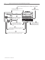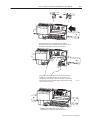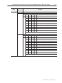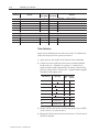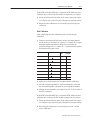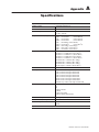
1
Allen-Bradley Thermocouple/ RTD/ Millivolt Input Module (Cat. No. 1794-IRT8) User Manual Important User Information Because of the variety of uses for the products described in this publication, those responsible for the application and use of this control equipment must satisfy themselves that all necessary steps have been taken to assure that each application and use meets all performance and safety requirements, including any applicable laws, regulations, codes and standards. The illustrations, charts, sample programs and layout examples shown in this guide are intended solely for example. Since there are many variables and requirements associated with any particular installation, Allen-Bradley does not assume responsibility or liability (to include intellectual property liability) for actual use based upon the examples shown in this publication. Allen-Bradley publication SGI–1.1, “Safety Guidelines For The Application, Installation and Maintenance of Solid State Control” (available from your local Allen-Bradley office) describes some important differences between solid-state equipment and electromechanical devices which should be taken into consideration when applying products such as those described in this publication. Reproduction of the contents of this copyrighted publication, in whole or in part, without written permission of Allen–Bradley Company, Inc. is prohibited. Throughout this manual we make notes to alert you to possible injury to people or damage to equipment under specific circumstances. ! ATTENTION: Identifies information about practices or circumstances that can lead to personal injury or death, property damage, or economic loss. Attention helps you: • identify a hazard • avoid the hazard • recognize the consequences Important: Identifies information that is especially important for successful application and understanding of the product. Important: We recommend you frequently backup your application programs on appropriate storage medium to avoid possible data loss. DeviceNet, DeviceNetManager, and RediSTATION are trademarks of Allen-Bradley Company, Inc. PLC, PLC–2, PLC–3, and PLC–5 are registered trademarks of Allen-Bradley Company, Inc. Windows is a trademark of Microsoft. Microsoft is a registered trademark of Microsoft IBM is a registered trademark of International Business Machines, Incorporated. All other brand and product names are trademarks or registered trademarks of their respective companies. Preface Objectives Read this preface to familiarize yourself with this manual and to learn how to use it properly and efficiently. Audience We assume that you have previously used an Allen-Bradley programmable controller, that you are familiar with its features, and that you are familiar with the terminology we use. If not, read the user manual for your processor before reading this manual. In addition, if using this module in a DeviceNet system, you must be familiar with: • DeviceNetManager Software, cat. no. 1787-MGR • Microsoft Windows Vocabulary In this manual, we refer to: • the individual Thermocouple/RTD/mV module as the “module,” or “TC/RTD module.” • the programmable controller as the “controller” or the “processor.” What This Manual Contains The contents of this manual are as follows: Chapter Title What’s Covered 1 Overview of Flex I/O and Your Thermocouple/RTD/mV Module Describes features, capabilities, and hardware components 2 How to Install Your TC/RTD/mV Input Module Installation and connecting wiring 3 Module Programming Block transfer programming and programming examples 4 Writing Configuration to and Reading Status from Your Module with a Remote I/O Adapter Describes block transfer write and block transfer read configurations, including complete bit/word descriptions 5 How Communication Takes Place and I/O Image Table Mapping with the DeviceNet Adapter Describes communication over the I/O backplane between the module and the adapter, and how data is mapped into the image table 6 Calibrating Your Module Lists the tools needed, and the methods used to calibrate the input module Specifications Module specifications and accuracy Appendix A Publication 1794-6.5.12 – November 1997 P–2 Using This Manual Conventions We use these conventions in this manual: In this manual, we show: Like this: that there is more information about a topic in another chapter in this manual that there is more information about the topic in another manual For Additional Information More For additional information on FLEX I/O systems and modules, refer to the following documents: Catalog C t og Number Publications Vo t g Voltage 1794 D c pt o Description Installation Instructions 1794 FLEX I/O Product Data 1794-2.1 User Manual 1794-ACN 24V dc ControlNet Adapter 1794-5.8 1794-ACNR 24V dc Redundant Media ControlNet Adapter 1794-5.18 1794-ACN15 24V dc ControlNet Adapter 1794-5.47 1794-ACNR15 24V dc Redundant Media ControlNet Adapter 1794-5.48 1794-ADN 24V dc DeviceNet Adapter 1794-5.14 1794-6.5.5 1794-ASB/C 24V dc Remote I/O Adapter 1794-5.50 1794-6.5.9 1794-ASB2/B 24V dc 2-Slot Remote I/O Adapter 1794-5.44 1794-6.5.13 1794-APB 24V dc Profibus Adapter 1794-5.40 1794-6.5.6 1794-IB8 24V dc 8 Sink Input Module 1794-5.30 1794-OB8 24V dc 8 Source Output Module 1794-5.31 1794-IB16 24V dc 16 Sink Input Module 1794-5.4 1794-OB16 24V dc 16 Source Output Module 1794-5.3 1794-IV16 24V dc 16 Source Input Module 1794-5.28 1794-OV16 24V dc 16 Sink Output Module 1794-5.29 1794-OB8EP 24V dc 8 Electronically Fused Output Module 1794-5.20 1794-IB8S 24V dc Sensor Input Module 1794-5.7 1794-IB10XOB6 24V dc 10 Input/6 Output Module 1794-5.24 1794-IE8 24V dc Selectable Analog 8 Input Module 1794-5.6 1794-OE4 24V dc Selectable Analog 4 Output Module 1794-5.5 1794-IE4XOE2 24V dc 4 Input/2 Output Analog Module 1794-5.15 Table continued on next page Publication 1794-6.5.12 – November 1997 1794-6.5.2 Using This Manual Publications Catalog Number Voltage 1794-OF4 24V dc 4 Output Isolated Analog Module 1794-5.37 1794-IF4 24V dc 4 Input Isolated Analog Module 1794-5.38 1794-IF2XOF2 24V dc 2 Input/2 Output Isolated Analog Module 1794-5.39 1794-IR8 24V dc 8 RTD Input Analog Module 1794-5.22 1794-6.5.4 1794-IT8 24V dc 8 Thermocouple Input Module 1794-5.21 1794-6.5.7 1794-IRT8 24V dc 8 Thermocouple/RTD Input Module 1794-5.50 1794-6.5.12 1794-IJ2 24V dc 2 Frequency Input Module 1794-5.49 1794-6.5.11 1794-IA8 120V ac 8 Input Module 1794-5.9 1794-OA8 120V ac Output Module 1794-5.10 1794-TB2 1794-TB3 2-wire Terminal Base 3-wire Terminal Base 1794-5.2 1794-TBN Terminal Base Unit 1794-5.16 1794-TBNF Fused Terminal Base Unit 1794-5.17 1794-TB3T Temperature Terminal Base Unit 1794-5.41 1794-TB3S Spring Clamp Terminal Base Unit 1794-5.42 1794-TB3TS Spring Clamp Temperature Base Unit 1794-5.43 1794-TB3G Terminal Base Unit 1794-5.51 1794-TB3GS Spring Clamp Terminal Base Unit 1794-5.59 Extender Cables 1794-5.12 Mounting Kit 1794-2.13 Power Supply 1794-5.35 1794-CE1, -CE3 1794-NM1 1794-PS1 Summary P–3 24V dc Description Installation Instructions User Manual 1794-6.5.8 This preface gave you information on how to use this manual efficiently. The next chapter introduces you to the Thermocouple/RTD/mV input module. Publication 1794-6.5.12 – November 1997 P–4 Using This Manual Publication 1794-6.5.12 – November 1997 Table of Contents Overview of FLEX I/O and Your Thermocouple/RTD/mV Input Module How to Install Your Thermocouple/RTD/mV Input Module Programming Your Thermocouple/RTD Input Module Chapter 1 What This Chapter Contains . . . . . . . . . . . . . . . . . . . . . . . . . . . . . What the Thermocouple/RTD/mV Input Modules Does . . . . . . . . . . How TC/RTD/mV Modules Communicate with Programmable Controllers . . . . . . . . . . . . . . . . . . . . . . . . . . . . Typical Communication Between an Adapter and a Module . . . Features of Your Module . . . . . . . . . . . . . . . . . . . . . . . . . . . . . . . Chapter Summary . . . . . . . . . . . . . . . . . . . . . . . . . . . . . . . . . . . . 1–1 1–1 1–1 1–2 1–3 1–3 Chapter 2 What This Chapter Contains . . . . . . . . . . . . . . . . . . . . . . . . . . . . . Before You Install Your Input Module . . . . . . . . . . . . . . . . . . . . . . . European Union Directive Compliance . . . . . . . . . . . . . . . . . . . . . . EMC Directive . . . . . . . . . . . . . . . . . . . . . . . . . . . . . . . . . . . . . Low Voltage Directive . . . . . . . . . . . . . . . . . . . . . . . . . . . . . . . . Power Requirements . . . . . . . . . . . . . . . . . . . . . . . . . . . . . . . . . . Wiring the Terminal Base Units (1794-TB3G shown) . . . . . . . . Installing the Module . . . . . . . . . . . . . . . . . . . . . . . . . . . . . . . . . . Mounting the Terminal Base Unit on a DIN Rail . . . . . . . . . . . . . Panel/Wall Mounting . . . . . . . . . . . . . . . . . . . . . . . . . . . . . . . . Mounting the Thermocouple/RTD/mV Module on the Terminal Base Unit . . . . . . . . . . . . . . . . . . . . . . . . . . . . . . . . . . . . . . Connecting Wiring for the TC/RTD/mV Module . . . . . . . . . . . . . . . . Wiring connections for the 1794-IRT8 TC/RTD/mV Input Module . Example of 2-, 3- and 4-wire RTD and Thermocouple Wiring to a 1794-TB3G Terminal Base Unit . . . . . . . . . . . . . . . . . . . . Module Indicators . . . . . . . . . . . . . . . . . . . . . . . . . . . . . . . . . . . . Chapter Summary . . . . . . . . . . . . . . . . . . . . . . . . . . . . . . . . . . . . 2–1 2–1 2–1 2–1 2–2 2–2 2–3 2–4 2–4 2–6 2–8 2–9 2–11 2–12 2–13 2–13 Chapter 3 What This Chapter Contains . . . . . . . . . . . . . . . . . . . . . . . . . . . . . Enter Block Transfer Instructions . . . . . . . . . . . . . . . . . . . . . . . . . . PLC-2 Family Processor . . . . . . . . . . . . . . . . . . . . . . . . . . . . . . PLC-3 Family Processor . . . . . . . . . . . . . . . . . . . . . . . . . . . . . . PLC-5 Family Processor . . . . . . . . . . . . . . . . . . . . . . . . . . . . . . PLC-5/250 Processor . . . . . . . . . . . . . . . . . . . . . . . . . . . . . . . . Chapter Summary . . . . . . . . . . . . . . . . . . . . . . . . . . . . . . . . . . . . 3–1 3–1 3–2 3–2 3–3 3–4 3–5 Publication 1794-6.5.12 – November 1997 ii Table of Contents Writing Configuration to and Reading Status from Your Module with a Remote I/O Adapter How Communication Takes Place and I/O Image Table Mapping with the DeviceNet Adapter Calibrating Your Module Chapter 4 What This Chapter Contains . . . . . . . . . . . . . . . . . . . . . . . . . . . . . Configuring Your Thermocouple/RTD/mV Input Module . . . . . . . . . . Sensor Types . . . . . . . . . . . . . . . . . . . . . . . . . . . . . . . . . . . . . . . Reading Data From Your Module . . . . . . . . . . . . . . . . . . . . . . . . . Mapping Data for the Thermocouple/RTD/mV Module . . . . . . . . . . . Thermocouple/RTD Input Module (1794-IRT8) Image Table Mapping . . . . . . . . . . . . . . . . . . . . . . . . . . . . . . . . . . Thermocouple/RTD/mV Input Module (1794-IRT8) Read Words Bit/Word Descriptions for the Thermocouple/RTD Input Module (1794-IRT8) Block Transfer Read Words . . . . . . . . . . . . . Thermocouple/RTD/mV Input Module (1794-IRT8) Write Words Bit/Word Definitions for the Block Transfer Write Words for the TC/RTD/mV Input Module . . . . . . . . . . . . . . . . . . . . . . . . Chapter Summary . . . . . . . . . . . . . . . . . . . . . . . . . . . . . . . . . . . . 4–3 4–3 4–4 4–5 4–5 4–9 Chapter 5 Chapter Objectives . . . . . . . . . . . . . . . . . . . . . . . . . . . . . . . . . . . About DeviceNetManager Software . . . . . . . . . . . . . . . . . . . . . . . . Polled I/O Structure . . . . . . . . . . . . . . . . . . . . . . . . . . . . . . . . . . . Adapter Input Status Word . . . . . . . . . . . . . . . . . . . . . . . . . . . . System Throughput . . . . . . . . . . . . . . . . . . . . . . . . . . . . . . . . . . . Mapping Data into the Image Table . . . . . . . . . . . . . . . . . . . . . . . . . . . . . . . . . . . . . . Thermocouple/RTD Input Module (1794-IRT8) Image Table Mapping . . . . . . . . . . . . . . . . . . . . . . . . . . . . . . . . . . Thermocouple/RTD Input Module (1794-IRT8) Read Words . . Thermocouple/RTD Input Module (1794-IRT8) Write Words . . . Bit/Word Descriptions for the Thermocouple/RTD/mV Input Module (1794-IRT8) . . . . . . . . . . . . . . . . . . . . . . . . Defaults . . . . . . . . . . . . . . . . . . . . . . . . . . . . . . . . . . . . . . . . . . . Chapter Summary . . . . . . . . . . . . . . . . . . . . . . . . . . . . . . . . . . . . 5–1 5–1 5–1 5–2 5–3 5–3 5–3 5–4 5–4 5–5 5–11 5–11 Chapter 6 What This Chapter Contains . . . . . . . . . . . . . . . . . . . . . . . . . . . . . When and How to Calibrate Your RTD/Thermocouple/mV Module . . Tools and Equipment . . . . . . . . . . . . . . . . . . . . . . . . . . . . . . . . . . Manually Calibrating your RTD/Thermocouple/mV Input Module . . . Calibration Setups . . . . . . . . . . . . . . . . . . . . . . . . . . . . . . . . . . Wiring Connections for Calibrating the TC/RTD/mV Input Module Read/Write Words for Calibration . . . . . . . . . . . . . . . . . . . . . . . EDT Calibration Command and Command Data . . . . . . . . . . . . . Offset Calibration . . . . . . . . . . . . . . . . . . . . . . . . . . . . . . . . . . . Gain Calibration . . . . . . . . . . . . . . . . . . . . . . . . . . . . . . . . . . . . Current Source Calibration . . . . . . . . . . . . . . . . . . . . . . . . . . . . Cold Junction Calibration . . . . . . . . . . . . . . . . . . . . . . . . . . . . . Publication 1794-6.5.12 – November 1997 4–1 4–1 4–2 4–3 4–3 6–1 6–1 6–2 6–2 6–3 6–3 6–4 6–5 6–6 6–7 6–8 6–8 iii Specifications Appendix A Specifications . . . . . . . . . . . . . . . . . . . . . . . . . . . . . . . . . . . . . . . A–1 Publication 1794-6.5.12 – November 1997 iv Table of Contents Publication 1794-6.5.12 – November 1997 Chapter 1 Overview of FLEX I/O and Your Thermocouple/RTD/mV Input Module What This Chapter Contains Read this chapter to familiarize yourself with the 1794-IRT8 module. For information on What the Thermocouple/RTD/mV Input Module Does . . . . . . . How the module communicates . . . . . . . . . . . . . . . . . . . . . . Module features . . . . . . . . . . . . . . . . . . . . . . . . . . . . . . . . . What the Thermocouple/RTD/mV Input Modules Does See page 1–1 1–1 1–3 The 1794-IRT8 module accepts up to 8 thermocouple or RTD inputs. The inputs are nonisolated and are selected with analog multiplexers which have a common–mode input range of +4 volts. The inputs will accept a millivolt or resistive input. Default input spans are –40.00mV to +100.00mV or 0.00 to 500.00 ohms. Fault Indicators are located on the field side. No switches or jumpers are used on the TC/RTD Input module. The Inputs have both fixed hardware filters and selectable firmware digital filters. How TC/RTD/mV Modules Communicate with Programmable Controllers FLEX I/O Thermocouple/RTD/mV modules are block transfer modules that interface analog signals with any Allen-Bradley programmable controllers that have block transfer capability. Block transfer programming moves input or output data words between the module’s memory and a designated area in the processor data table. Block transfer programming also moves configuration words from the processor data table to module memory. The adapter/power supply transfers data to the module (block transfer write) and from the module (block transfer read) using BTW and BTR instructions in your ladder diagram program. These instructions let: • the adapter obtain input or output values and status from the module • you establish the module’s mode of operation. The illustration describes the communication process. Publication 1794-6.5.12 – November 1997 1–2 Overview of FLEX I/O and Your Thermocouple/RTD/mV Input Module Typical Communication Between an Adapter and a Module 1 2 The adapter transfers your configuration data to the module using a BTW. External devices transmit analog signals to the module. Flexbus Allen-Bradley Allen-Bradley 1794–IRT8 TC RTD INPUT 8 CHANNEL ADAPTER ACTIVE FAULT LOCAL FAULT 3 4 24VDC POWER SUPPLY RIO ADAPTER 1794-ASB Your ladder program instructs the adapter to perform a BTR of the values and stores them in a data table. PWR IN 0 F 5 The adapter and module determine that the transfer was made without error and input values are within specified range. 6 Your ladder program can use and/or move the data (if valid) before it is written over by the transfer of new data in a subsequent transfer. 7 Your ladder program performs BTWs to the module only when you power it up, or any time you wish to reconfigure the module. Publication 1794-6.5.12 – November 1997 IN 1 F IN 2 F IN 3 F IN 4 F IN 5 F IN 6 F IN 7 F 3 The module converts analog signals into binary format and stores these values until the adapter requests their transfer. Overview of FLEX I/O and Your Thermocouple/RTD/mV Input Module Features of Your Module 1–3 The module label identifies the keyswitch position, wiring and module type. A removable label provides space for writing individual designations per your application. Indicators are provided to identify input fault conditions, and to show when power is applied to the module. 1794-IRT8 Module Type Removable Label Allen-Bradley 1794–IRT8 TC RTD INPUT 8 CHANNEL 3 Keyswitch Position Indicator (#3) PWR IN 0 F IN 1 F IN 2 F IN 3 F IN 4 F IN 5 F IN 6 F IN 7 F Power On Indicator Input Designators Chapter Summary In this chapter, we told you about the FLEX I/O system and the Thermocouple/RTD/mV input module, and how they communicate with programmable controllers. Publication 1794-6.5.12 – November 1997 1–4 Overview of FLEX I/O and Your Thermocouple/RTD/mV Input Module Publication 1794-6.5.12 – November 1997 Chapter 2 How to Install Your Thermocouple/RTD/mV Input Module What This Chapter Contains Before You Install Your Input Module In this chapter, we tell you: For information on See page Before You Install Your Module . . . . . . . . . . . . . . . . . . . . . . . European Union Directives . . . . . . . . . . . . . . . . . . . . . . . . . . Power Requirements . . . . . . . . . . . . . . . . . . . . . . . . . . . . . . Installing the Module . . . . . . . . . . . . . . . . . . . . . . . . . . . . . . on a DIN rail . . . . . . . . . . . . . . . . . . . on a wall/panel on the terminal base Connecting Wiring . . . . . . . . . . . . . . . . . . . . . . . . . . . . . . . . Module Indicators . . . . . . . . . . . . . . . . . . 2–1 2–1 2–2 2–4 2–4 2–6 2–8 2–9 2–13 Before installing your TC/RTD/mV module: You need to: As described under: Calculate the power requirements of all modules in this FLEX system. Power Requirements, page 2-2 Position the keyswitch on the terminal base Installing the Module, page 2–4 ! European Union Directive Compliance ATTENTION: The TC/RTD/mV module does not receive power from the backplane. +24V dc power must be applied to your module before installation. If power is not applied, the module position will appear to the adapter as an empty slot in your chassis. If this product has the CE mark it is approved for installation within the European Union and EEA regions. It has been designed and tested to meet the following directives. EMC Directive This product is tested to meet Council Directive 89/336/EEC Electromagnetic Compatibility (EMC) and the following standards, in whole or in part, documented in a technical construction file: • EN 50081-2EMC – Generic Emission Standard, Part 2 – Industrial Environment • EN 50082-2EMC – Generic Immunity Standard, Part 2 – Industrial Environment This product is intended for use in an industrial environment. Publication 1794-6.5.12 – November 1997 2–2 How to Install Your Thermocouple/RTD/mV Input Module Low Voltage Directive This product is tested to meet Council Directive 73/23/EEC Low Voltage, by applying the safety requirements of EN 61131–2 Programmable Controllers, Part 2 – Equipment Requirements and Tests. For specific information required by EN 61131-2, see the appropriate sections in this publication, as well as the following Allen-Bradley publications: • Industrial Automation Wiring and Grounding Guidelines For Noise Immunity, publication 1770-4.1 • Guidelines for Handling Lithium Batteries, publication AG-5.4 • Automation Systems Catalog, publication B111 This equipment is classified as open equipment and must be mounted in an enclosure during operation to provide safety protection. Power Requirements The wiring of the terminal base unit is determined by the current draw through the terminal base. Make certain that the current draw does not exceed 10A. ! Publication 1794-6.5.12 – November 1997 ATTENTION: Total current draw through the terminal base unit is limited to 10A. Separate power connections may be necessary. How to Install Your Thermocouple/RTD/mV Input Module 2–3 Methods of wiring the terminal base units are shown in the illustration below. Wiring the Terminal Base Units (1794-TB3G shown) ! ATTENTION: Do not daisy chain power or ground from the terminal base unit to any ac or dc digital module terminal base unit. Daisy-chaining TC/RTD/mV Module 24V dc TC/RTD/mV Module TC/RTD/mV Module Frequency Input Module Note: All modules must be frequency or TC/RTD/mV modules for this configuration. Wiring when total current draw is less than 10A Individual Digital Input Module TC/RTD/mV Module Digital Input Module Digital Output Module 24V dc 24V dc Note: Use this configuration if using any “noisy” dc digital I/O modules in your system. 24V dc Thermocouple/RTD/mV Module wiring separate from digital wiring. Wiring when total current draw is greater than 10A Combination Frequency Input Module Frequency Input Module TC/RTD/mV Module Frequency Input Module 24V dc 24V dc Note: All modules powered by the same power supply must be frequency or TC/RTD/mV modules for this configuration. Total current draw through any base unit must not be greater than 10A Publication 1794-6.5.12 – November 1997 2–4 How to Install Your Thermocouple/RTD/mV Input Module Installing the Module Installation of the analog module consists of: • mounting the terminal base unit • installing the TC/RTD/mV module into the terminal base unit • installing the connecting wiring to the terminal base unit If you are installing your module into a terminal base unit that is already installed, proceed to “Mounting the Thermocouple/RTD/mV Module on the Terminal Base” on page 2–8. Mounting the Terminal Base Unit on a DIN Rail ! ATTENTION: Do not remove or replace a terminal base unit when power is applied. Interruption of the flexbus can result in unintended operation or machine motion. 1. Remove the cover plug (if used) in the male connector of the unit to which you are connecting this terminal base unit. 2. Check to make sure that the 16 pins in the male connector on the adjacent device are straight and in line so that the mating female connector on this terminal base unit will mate correctly. 3. Position the terminal base on the 35 x 7.5mm DIN rail A (A-B pt. no. 199-DR1; 46277-3) at a slight angle with hook B on the left side of the terminal base hooked into the right side of the unit on the left. Proceed as follows: B A A Position terminal base at a slight angle and hooked over the top of the DIN rail. Publication 1794-6.5.12 – November 1997 How to Install Your Thermocouple/RTD/mV Input Module 2–5 Slide the terminal base unit over tight against the adapter. Make sure the hook on the terminal base slides under the edge of the adapter and the flexbus connector is fully retracted. Press down on the terminal base unit to lock the terminal base on the DIN rail. If the terminal base does not lock into place, use a screwdriver or similar device to open the locking tab, press down on the terminal base until flush with the DIN rail and release the locking tab to lock the base in place. 30077–M Gently push the flexbus connector into the side of the adapter to complete the backplane connection. Publication 1794-6.5.12 – November 1997 2–6 How to Install Your Thermocouple/RTD/mV Input Module 4. Repeat the above steps to install the next terminal base. Panel/Wall Mounting Installation on a wall or panel consists of: • • • • laying out the drilling points on the wall or panel drilling the pilot holes for the mounting screws mounting the adapter mounting plate installing the terminal base units and securing them to the wall or panel If you are installing your module into a terminal base unit that is already installed, proceed to “Mounting the Thermocouple/RTD/mV Module on the Terminal Base” on page 2–8. Use the mounting kit Cat. No. 1794-NM1 for panel/wall mounting. 1.4 (35.5) 1794-NM1 Mounting Kit Contents: 1 – Mounting Plate for Adapter 2 – 18 #6 self-tapping screws (2 for the adapter, and 2 each for up to 8 modules) 1 2 Adapter Module (not included) Terminal Base Unit (not included) Publication 1794-6.5.12 – November 1997 How to Install Your Thermocouple/RTD/mV Input Module 2–7 To install the mounting plate on a wall or panel: 1. Lay out the required points on the wall/panel as shown in the drilling dimension drawing. Drilling Dimensions for Panel/Wall Mounting of FLEX I/O Inches (Millimeters) 1.4 (35.5) 2.3 (58.5) 1.4 (35.5) 2.3 (58.5) 1.4 (35.5) .83 (21) 2. Drill the necessary holes for the #6 self-tapping mounting screws. 3. Mount the mounting plate (1) for the adapter module using two #6 self-tapping screws (18 included for mounting up to 8 modules and the adapter). Important: More Make certain that the mounting plate is properly grounded to the panel. Refer to “Industrial Automation Wiring and Grounding Guidelines,” publication 1770-4.1. 4. Hold the adapter (2) at a slight angle and engage the top of the mounting plate in the indention on the rear of the adapter module. 5. Press the adapter down flush with the panel until the locking lever locks. 6. Position the terminal base unit up against the adapter and push the female bus connector into the adapter. 7. Secure to the wall with two #6 self-tapping screws. 8. Repeat for each remaining terminal base unit. Note: The adapter is capable of addressing eight modules. Do not exceed a maximum of eight terminal base units in your system. Publication 1794-6.5.12 – November 1997 2–8 How to Install Your Thermocouple/RTD/mV Input Module Mounting the Thermocouple/RTD/mV Module on the Terminal Base Unit The TC/RTD/mV input module mounts on a 1794-TB3G or TB3GS terminal base unit. 1. Rotate the keyswitch (1) on the terminal base unit (2) clockwise to position 3 as required for the TC/RTD/mV module. 7 3 1 2 6 4 5 2. Make certain the flexbus connector (3) is pushed all the way to the left to connect with the neighboring terminal base/adapter. You cannot install the module unless the connector is fully extended. 3. Make sure that the pins on the bottom of the module are straight so they will align properly with the connector in the terminal base unit. ! ATTENTION: Remove field-side power before removing or inserting the module. This module is designed so you can remove and insert it under backplane power. When you remove or insert a module with field-side power applied, an electrical arc may occur. An electrical arc can cause personal injury or property damage by: • sending an erroneous signal to your system’s field devices causing unintended machine motion • causing an explosion in a hazardous environment Repeated electrical arcing causes excessive wear to contacts on both the module and its mating connector. Worn contacts may create electrical resistance. 4. Position the module (4) with its alignment bar (5) aligned with the groove (6) on the terminal base. Publication 1794-6.5.12 – November 1997 How to Install Your Thermocouple/RTD/mV Input Module 2–9 5. Press firmly and evenly to seat the module in the terminal base unit. The module is seated when the latching mechanism (7) is locked into the module. 6. Repeat the above steps to install the next module in its terminal base unit. Connecting Wiring for the TC/RTD/mV Module Wiring to the TC/RTD/mV module is made through the terminal base unit on which the module mounts. Compatible terminal base units are: Module 1794-TB3G 1794-TB3GS 1794-IRT8 Yes Yes 1794-TB3G 1794-TB3GS 0 1 2 3 4 5 6 7 8 9 10 11 12 13 14 15 16 17 18 19 20 21 22 23 24 25 26 27 28 29 30 31 32 33 34 35 36 37 38 39 40 41 42 43 44 45 46 47 48 49 50 51 0 1 2 3 4 5 6 7 8 9 10 11 12 13 14 15 A 0 –15 A B 16–33 B C 34–51 C Label placed at top of wiring area. 16 17 18 19 20 21 22 23 24 25 26 27 28 29 30 31 32 33 34 35 36 37 38 39 40 41 42 43 44 45 46 47 48 49 50 51 34 and 50 = 24V dc 35 and 51 = common 16 and 33 = chassis ground 40 thru 45 = chassis ground 34 and 50 = 24V dc 35 and 51 = common 16 and 33 = chassis ground 40 thru 45 = chassis ground Connecting Wiring using a 1794-TB3G and -TB3GS Terminal Base Units 1. Connect the individual signal wiring to numbered terminals on the 0–15 row (A) and 17–32 row (B) on the terminal base unit. Connect the input devices as shown in the wiring table on page 2–11. 2. Terminate shields:to terminals 16 or 33 on row B, or 40 through 45 on row C. 3. Connect +24V dc to terminal 34 on the 34-51 row (C), and 24V common to terminal 35 on the 34-51 row (C). Publication 1794-6.5.12 – November 1997 2–10 How to Install Your Thermocouple/RTD/mV Input Module ATTENTION: To reduce susceptibility to noise, power TC/RTD/mV modules and digital modules from separate power supplies. Do not exceed a length of 33 ft (10m) for dc power cabling. ! 4. If daisy chaining the +24V dc power to the next base unit, connect a jumper from terminal 50 (+24V) on this base unit to terminal 34 and from terminal 51 (24V dc common) to terminal 35 on the next base unit. ATTENTION: Do not daisy chain power or ground from the TC/RTD/mV terminal base unit to any ac or dc digital module terminal base unit. ! ATTENTION: The TC/RTD/mV modules do not receive power from the backplane. +24V dc power must be applied to your module before operation. If power is not applied, the module position will appear to the adapter as an empty slot in your chassis. If the adapter does not recognize your module after installation is completed, cycle power to the adapter. ! Connections for Terminal Base 1794-TB3G shown 0 1 + 2 3 H L Channel 0 – 17 16 + 18 19 H L Channel 4 4 + 5 6 7 8 H L Channel 1 – + 20 – 21 + 22 23 H L Channel 5 9 24 – 10 11 12 H L Channel 2 – + 25 + 26 27 H L Channel 6 13 14 15 H L Channel 3 – 28 29 – + 30 31 H L Channel 7 Chassis Gnd 35 34 +V COM 24V dc Supply In Publication 1794-6.5.12 – November 1997 32 33 – Chassis Gnd 36 37 Gnd CJC 38 39 40 41 42 43 6 Chassis Ground for Shields 44 45 46 47 Gnd CJC 48 49 50 +V 51 COM 24V dc Supply Out How to Install Your Thermocouple/RTD/mV Input Module RTD 1 Wiring connections for the 1794-IRT8 TC/RTD/mV Input Module 2 2-wire 3-wire Connect the following: Typ of Type o Input I p t 1 3 2 H 4-wire 1 1a 2a 2 L + – 1 2 3 1 2 2a 1 2 RTD – 2-wire RTD – 3-wire RTD – 4-wire Thermocouple 2–11 1a Thermocouple 1 2 Millivolt 1 2 Shield1 1 Terminals 37, 38 and 39 and 46, 47 and 48 are for cold junction compensation (with 38 and 47 chassis GND). 1 2 1 Millivolt + mV – 2 1794-TB3G and -TB3GS Terminal Base Units RTD or Th moco p Thermocouple Channel High Signal Terminal (H) Low Signal Terminal (L) RTD Source Current (+) Signal Return1 (–) 0 1 2 0 3 1 5 6 4 7 2 9 10 8 11 3 13 14 12 15 4 18 19 17 20 5 22 23 21 24 6 26 27 25 28 7 30 31 29 32 +24V dc Power 34 and 50 24V dc Common 35 and 51 1 Terminals 37, 38 and 39 and 46, 47 and 48 are for cold junction compensation (with 38 and 47 chassis GND). Connect CJC1 to terminal 5 or 21; CJC2 to terminal 12 or 29. 2 Terminals 16, 33 and 40 thru 45 are chassis ground. ! ATTENTION: Total current draw through the terminal base unit is limited to 10A. Separate power connections to the terminal base unit may be necessary. Publication 1794-6.5.12 – November 1997 2–12 How to Install Your Thermocouple/RTD/mV Input Module Example of 2-, 3- and 4-wire RTD and Thermocouple Wiring to a 1794-TB3G Terminal Base Unit Thermocouple Channel 4 1 + 2 – 2-Wire RTD Channel 1 1 2 3-Wire RTD Channel 2 1 3 2 4-Wire RTD Channel 3 1 1a 2a 2 0 1 0 1 17 16 34 2 18 35 3 2 3 19 36 4 4 20 37 5 5 21 38 6 6 22 39 7 7 23 40 8 8 24 41 9 9 25 42 10 10 26 43 11 11 27 44 12 12 28 45 13 13 29 46 14 14 30 47 15 15 31 48 32 49 33 50 51 0 –15 A 16–33 B 34–51 C 1794-TB3G CJC Attention: Keep exposed area of inner conductor as short as possible. Publication 1794-6.5.12 – November 1997 How to Install Your Thermocouple/RTD/mV Input Module Module Indicators 2–13 The Thermocouple/RTD/mV module has one status indicator (PWR) that is on when power is applied to the module and one fault indicator (F) for each input. Allen-Bradley 1794–IRT8 TC RTD INPUT 8 CHANNEL 3 IN 0 F IN 1 F IN 2 F A IN 3 F IN 4 F IN 5 F IN 6 F B IN 7 F PWR C A = Insertable label for writing individual input designations B = Fault Indicator – indicates successful power up or noncritical fault C = Power Indicator – indicates power applied to module Indicator Fault Color Red State On Meaning At power up – Channel 0 indicator lights at powerup until all internal diagnostics are checked. After successful powerup, the indicator goes off if no fault is present. After successful powerup – Indicates a critical fault (diagnostic failure, etc.) Power Green Chapter Summary Blinking (when faults are enabled, and bit set) Indicates a noncritical fault (such as open sensor.) Input data set to maximum, and indicator flashes at 1Hz rate. Off Module not powered On Module receiving power. In this chapter, we told you how to install your input module in an existing programmable controller system and how to wire to the terminal base units. Publication 1794-6.5.12 – November 1997 2–14 How to Install Your Thermocouple/RTD/mV Input Module Publication 1794-6.5.12 – November 1997 Chapter 3 Programming Your Thermocouple/RTD Input Module What This Chapter Contains To initiate communication between the Thermocouple/RTD input module and your PLC processor, you must enter block transfer instructions into your ladder logic program. Use this chapter to enter the necessary block transfer instructions into your ladder logic program. To edit your ladder logic you Enter Block Transfer Instructions . . . . . . . . . . . . . . . . . . . . . PLC-2 Family Processors . . . . . . . . . . . . . . . . . . . . . . . . PLC-3 Family Processors . . . . . . . . . . . . . . . . . . . . . . . . PLC-5 Family Processors . . . . . . . . . . . . . . . . . . . . . . . . PLC-5/250 Processors . . . . . . . . . . . . . . . . . . . . . . . . . . Enter Block Transfer Instructions See page 3–1 3–2 3–2 3–3 3–4 The Thermocouple/RTD input module communicates with the PLC processor through bidirectional block transfers. This is the sequential operation of both read and write block transfer instructions. Before you configure the module, you need to enter block transfer instructions into your ladder logic. The following example programs illustrate the minimum programming required for communication to take place between the module and a PLC processor. These programs can be modified to suit your application requirements. A configuration block transfer write (BTW) is initiated when the analog module is first powered up, and subsequently only when the programmer wants to enable or disable features of the module. The configuration BTW sets the bits which enable the programmable features of the module, such as filters and signal ranges, etc. Block transfer reads are performed to retrieve information from the module. Block transfer read (BTR) programming moves status and data from the module to the processor’s data table. The processor user program initiates the request to transfer data from the module to the processor. The transferred words contain module status, channel status and input data from the module. Your program should monitor status bits, block transfer read and block transfer write activity. Publication 1794-6.5.12 – November 1997 3–2 Programming Your Thermocouple/RTD Input Module PLC-2 Family Processor The 1794 Thermocouple/RTD/mV modules are not recommended for use with PLC-2 family programmable controllers due to the number of digits needed for high resolution. Important: The Thermocouple/RTD input module functions with reduced performance in PLC-2 systems. Because the module does not support BCD and the PLC-2 processor is limited to values of 4095 (12 bit binary), many values returned in the BTR file may not provide meaningful data to the PLC-2 processor. PLC-3 Family Processor Block transfer instructions with the PLC-3 processor use a control file and a data file. The block transfer control file contains the data table section for module location, the address of the block transfer data file and other related data. The block transfer data file stores data that you want transferred to the module (when programming a BTW) or from the module (when programming a BTR). The programming terminal prompts you to create a control file when a block transfer instruction is being programmed. The same block transfer control file is used for both the read and write instructions for your module. A different block transfer control file is required for every module. Publication 1794-6.5.12 – November 1997 Programming Your Thermocouple/RTD Input Module PLC-3 Processor Program Example 3–3 Rung M:0 The IRT8 module is located in rack 3, I/O group 2, slot 1. The control file is a 10 word file starting at B17:0 that is shared by the BTR/BTW. The data obtained by the PLC3 processor is placed in memory starting at location N18:101, and with the default length of 0, is 11 words long. IRT8 BTR/BTW Control Block BTR BLOCK TRANSFER READ Rack 3 Group 2 Slot 1 Control B17:0 Data File N18:101 Length 0 IRT8 BTR Done Bit B17:0 15 EN DN ER IRT8 BTR Error Bit B17:0 U 13 IRT8 BTR Error Bit B17:0 13 The IRT8 module is located in rack 3, I/O group 2, slot 1. The control file is a 10 word file starting at B17:0 that is shared by the BTR/BTW. The data sent by the PLC-3 processor to the IRT8 module is from PLC memory starting at N18:1, and with the default length of 0, is 4 words long. IRT8 BTR/BTW Control Block IRT8 BTW Done Bit B17:0 BTW BLOCK TRANSFER WRITE Rack 3 Group 2 Slot 1 Control B17:0 Data N18:1 Length 0 5 IRT8 BTW Error Bit B17:0 EN DN ER IRT8 BTW Error Bit B17:0 U 3 3 PLC-5 Family Processor Block transfer instructions with the PLC-5 processor use a control file and a data file. The block transfer control file contains the data table section for module location, the address of the block transfer data file and other related data. The block transfer data file stores data that you want transferred to the module (when programming a BTW) or from the module (when programming a BTR). The programming terminal prompts you to create a control file when a block transfer instruction is being programmed. A different block transfer control file is used for the read and write instructions for your module. Publication 1794-6.5.12 – November 1997 3–4 PLC-5 Processor Program Example Programming Your Thermocouple/RTD Input Module Rung 2:0 The IRT8 module is located in rack 2, I/O group 2, slot 1. The integer control file starts at N22:200, is 5 words long and is compatible with all PLC-5 family members. The data obtained by the PLC-5 processor from the IRT8 module is placed in memory starting at N22:101, and with the default length of 0, is 11 words long. The length can be any number between 0 and 11. In enhanced PLC-5 processors➀, the block transfer data type may be used as a control file. IRT8 BTR IRT8 BTW IRT8 BTR Control File Enable Bit BTR Enable Bit BLOCK TRANSFER READ EN N22:205 N22:200 Rack 02 Group 2 DN Slot 1 15 15 Control N22:200 ER Data File N22:101 Length 0 Continuous N Rung 2:1 The IRT8 module is located in rack 2, group 2, slot 1. The integer control file starts at N22:205, is a 5 words long and is compatible will all PLC-5 family members. The data sent by the PLC-5 processor to the IRT8 module starts at N22:1, and with the default length of 0, is 4 words long. Valid BTW lengths: 0, 1, 2, 3, and 4. In enhanced PLC-5 processors1, the block transfer data type may be used as a control file. IRT8 BTR Enable Bit IRT8 BTW Enable Bit N22:200 N22:205 15 15 ➀ Enhanced IRT8 BTW Control File BTW BLOCK TRANSFER WRITE Rack 02 Group 2 Slot 1 Control N22:205 Data File N22:1 Length 0 Continuous N EN DN ER PLC-5 processors include: PLC-5/11, -5/20, -5/3x, -5/4x, and -5/6x. PLC-5/250 Processor Block transfer instructions with the PLC-5/250 processor use a control file and a data file. The block transfer control file contains the data table section for module location, the address of the block transfer data file and other related data. The block transfer data file stores data that you want transferred to the module (when programming a BTW) or from the module (when programming a BTR). The programming terminal will automatically select the control file based on rack, group and module, and whether it is a read or write. A different block transfer control file is used for the read and write instructions for your module. A different block transfer control file is required for every module. Publication 1794-6.5.12 – November 1997 Programming Your Thermocouple/RTD Input Module PLC-5/250 Processor Program Example 3–5 Rung 1STEPO:1 The IRT8 module is located in rack 14, I/O group 1, slot 0. The data obtained by the PLC-5/250 processor from the IRT8 module is placed in the data table starting at 2BTD5:101, and with the default length of 0, is 11 words long. The length can be any number between 0 and 11. IRT8 BTR IRT8 BTW IRT8 BTR Control File Enable Bit BTR Enable Bit BLOCK TRANSFER READ EN BW141:0 BR141:0 Rack 14 Group 1 DN Slot 0 EN EN Control Block BR141:0 ER Data File 2BTD5:101 BT Length 0 Continuous NO BT Timeout 4 Rung 1STEPO:1 The IRT8 module is located in rack 14, I/O group 1, slot 0. The data sent to the IRT8 module from the PLC-5/250 processor is from the data table starting at 2BTD5:1, and with a default length of 0, is 4 words long. Valid BTW lengths: 0, 1, 2, 3, and 4. IRT8 BTR Enable Bit BR141:0 EN Chapter Summary IRT8 BTW Enable Bit BW141:0 IRT8 BTW Control File BTW BLOCK TRANSFER WRITE Rack 14 Group 1 Slot 0 Control Block BW141:0 Data File 2BTD5:1 BT Length 0 Continuous NO 4 BT Timeout EN EN DN ER In this chapter, you learned how to program with your IRT8 input module using block transfer instructions and ladder logic. Now, you can configure your module. 4 Configure the IRT8 Module Publication 1794-6.5.12 – November 1997 3–6 Programming Your Thermocouple/RTD Input Module Publication 1794-6.5.12 – November 1997 Chapter 4 Writing Configuration to and Reading Status from Your Module with a Remote I/O Adapter What This Chapter Contains Configuring Your Thermocouple/RTD/mV Input Module In this chapter, we tell you about: For information on See page Configuring Your Module . . . . . . . . . . . . . . . . . . . . . . . . . . . Sensor Type . . . . . . . . . . . . . . . . . . . . . . . . . . . . . . . . . . . . Reading Data from Your Module . . . . . . . . . . . . . . . . . . . . . . Mapping Data for the Module . . . . . . . . . . . . . . . . . . . . . . . . TC/RTD Input Module (1794-IRT8) Image Table Mapping . . . . Block Transfer Read Word Assignments . . . . . . . . . . . . . . . . Bit/Word Definitions for Block Transfer Read Words . . . . . . . . Block Transfer Write Word Assignments . . . . . . . . . . . . . . . . Bit/Word Definitions for the Block Transfer Write Words . . . . . 4–1 4–2 4–3 4–3 4–3 4–3 4–4 4–5 4–5 The TC/RTD/mV input module is configured using a group of data table words that are transferred to the module using a block transfer write instruction. The software configurable features available are: • input range selection • selectable single pole low pass filter • data reported in oF, oC, oK, mV, ohms, unipolar or bipolar count Note: Programmable controllers that use 6200 software (release 4.2 or higher) programming tools can take advantage of the IOCONFIG Addendum utility to configure this module. IOCONFIG Addendum uses menu–based screens for configuration without having to set individual bits in particular locations. Refer to your 6200 software literature for details. Important: It is strongly recommended that you use IOCONFIG Addendum to configure this module. The IOCONFIG Addendum utility greatly simplifies configuration. If the IOCONFIG Addendum is not available, you must enter data directly into the data table. Use this chapter as a reference when performing this task. Publication 1794-6.5.12 – November 1997 4–2 Writing Configuration to and Reading Status from Your Module with a Remote I/O Adapter Sensor Types Individual input channels are configurable to operate with the following sensor types: RTD Type Sensor type for channels 0 through 3 Sensor type for channels 4 through 7 Resistance (default) 100 ohm Pt α = 0.00385 Euro (–200 to +870oC) 200 ohm Pt α = 0.00385 Euro (–200 to +400oC) 100 ohm Pt α = 0.003916 U.S. (–200 to +630oC) 200 ohm Pt α = 0.003916 U.S. (–200 to +400oC) 100 ohm Nickel α = 0.00618 (–60 to +250oC) 200 ohm Nickel α = 0.00618 (–60 to +200oC) 120 ohm Nickel α = 0.00672 (–80 to +320oC) 10 ohm Copper α = 0.00427 (–200 to +260oC) Thermocouple Type Sensor type for channels 0 through 3 Sensor type for channels 4 through 7 mV (default) B 300 to 1800oC (572 to 3272oF) E –270 to 1000oC (–454 to 1832oF) J –210 to 1200oC (–346 to 2192oF) K –270 to 1372oC (–454 to 2502oF) L -200 to 800oC (-328 to 1472oF) N –270 to 1300oC (–450 to 2372oF) R –50 to 1768oC (–58 to 3214oF) S –50 to 1768oC (–58 to 3214oF) T –270 to 400oC (–454 to 752oF) You select individual channel ranges using write word 1 of the block transfer write instruction. Publication 1794-6.5.12 – November 1997 Writing Configuration to and Reading Status from Your Module with a Remote I/O Adapter 4–3 Reading Data From Your Module Read programming moves status and data from the TC/RTD input module to the processor’s data table in one I/O scan. The processor’s user program initiates the request to transfer data from the TC/RTD input module to the processor. Mapping Data for the Thermocouple/RTD/mV Module The following read and write words and bit/word descriptions describe the information written to and read from the TC/RTD input module. The module uses up to 11 words of input data and up to 4 words of output data. Each word is composed of 16 bits. Thermocouple/RTD Input Module (1794-IRT8) Image Table Mapping Module Image Input Data Channel 0 Input Data Channel 1 I/O Image Input Data Channel 2 Input Size Input Data Channel 3 1 to 11 Words Input Data Channel 4 Input Data Channel 5 Input Data Channel 6 Input Data Channel 7 Overrange Underrange Alarms Output Size RFlg CJC Diagnostics EDT command and response Data Format 0 to 4 Words TC/RTD Mode Sensor Type FM Reference Jct Filter Cut TC/RTD Mode Sensor Type RTD Offsets for each channel CFlg EDT command and data Thermocouple/RTD/mV Input Module (1794-IRT8) Read Words Decimal 15 14 13 12 11 10 09 08 07 06 05 04 03 02 01 00 Octal 17 16 15 14 13 12 11 10 07 06 05 04 03 02 01 00 Word⇓ Read 0 Channel 0 Input Data 1 Channel 1 Input Data 2 Channel 2 Input Data 3 Channel 3 Input Data 4 Channel 4 Input Data 5 Channel 5 Input Data 6 Channel 6 Input Data 7 Channel 7 Input Data Publication 1794-6.5.12 – November 1997 4–4 Writing Configuration to and Reading Status from Your Module with a Remote I/O Adapter Decimal 15 14 13 12 11 10 09 08 07 06 05 04 03 02 01 00 Octal 17 16 15 14 13 12 11 10 07 06 05 04 03 02 01 00 8 Overrange Alarm Bits (channel 0 = bit 08, etc) 9 Flt Alm Ch7 10 Resp Flg Flt Alm Ch5 Flt Alm Ch6 Flt Alm Ch4 Flt Alm Ch3 Flt Alm Ch2 Underrange Alarm Bits (channel 0 = bit 00, etc) Flt Alm Ch1 Flt Alm CJC 2 CJC 1 Rsvd Rsvd Ch0 Alm Alm EDT command response Diagnostic Status EDT response data Bit/Word Descriptions for the Thermocouple/RTD Input Module (1794-IRT8) Block Transfer Read Words Word Dec. Bits (Octal Bits) Description Read Word 0 00–15 (00–17) Channel 0 Input data Read Word 1 00–15 (00–17) Channel 1 Input data Read Word 2 00–15 (00–17) Channel 2 Input data Read Word 3 00–15 (00–17) Channel 3 Input data Read Word 4 00–15 (00–17) Channel 4 Input data Read Word 5 00–15 (00–17) Channel 5 Input data Read Word 6 00–15 (00–17) Channel 6 Input data Read Word 7 00–15 (00–17) Channel 7 Input data Read Word 8 00–07 08–15 (10–17) Read Word 9 00–03 Underrange bits – these bits are set if the input signal is below the input channel’s minimum range. Bit 00 corresponds to channel 0, bit 01 corresponds to channel 1, etc. Overrange bits – these bits are set if 1), the input signal is above the input channel’s maximum range, or 2), an open detector is detected. Bit 08 (10) corresponds to channel 0, bit 09 (11) corresponds to channel 1, etc. Diagnostic bits – represent module configuration and/or hardware errors. Bit 03 02 01 00 0 0 0 0 Reserved for factory use 0 0 1 0 Improper module configuration 0001 and 0011 thru 1111 Reserved for factory use 04 05–06 07 08–15 (10–17) Read Word 10 00–07 08–14 (10–16) 15 (17) Publication 1794-6.5.12 – November 1997 Not used. Cold junction compensation alarm bits – These bits are set (1) when the corresponding cold junction compensator lead is broken, unattached or shorted. Bit 05 corresponds to CJC1, and bit 06 to CJC2. Not used Fault alarm bits – An alarm bit is set (1) when an individual input lead opens (broken, disconnected). If the alarm is enabled, the channel reads maximum value. Bit 08 (10) corresponds to input channel 0, bit 09 (11) to channel 1, etc. Extended data table command response data bits – These bits echo the EDT command data written to the module during calibration. Extended data table command response bits – These bits echo the EDT command written to the module during calibration. Reserved for factory use Writing Configuration to and Reading Status from Your Module with a Remote I/O Adapter 4–5 Thermocouple/RTD/mV Input Module (1794-IRT8) Write Words Output Mapping Decimal ct Octal 15 14 13 12 11 10 09 08 07 06 05 04 03 02 01 00 17 16 15 14 13 12 11 10 07 06 05 04 03 02 01 00 Flt Mode Ch 0-3 Flt Mode Ch 4-7 Write Word⇓ 0 Not used Data Format 1 TC/RTD Ch. 4-7 Sensor Mode Ch. 4-7 2 RTD Offset Ch 7 RTD Offset Ch 6 3 Cmd Flag Sensor Mode Ch. 4-7 RTD Offset Ch 5 RTD Offset Ch 4 Reference Jct. TC/RTD Ch. 0-3 Sensor Mode Ch. 0-3 RTD Offset Ch 3 RTD Offset Ch 2 EDT command Filter Cutoff Sensor Mode Ch. 0-3 RTD Offset Ch 1 RTD Offset Ch 0 EDT command data Bit/Word Definitions for the Block Transfer Write Words for the TC/RTD/mV Input Module Word Dec. Bits (Octal Bits) Write Word 0 00–02 Description Input Filter Cutoff bits Bit Bits 03–05 02 01 00 Definition 0 0 0 Hardware filtering only (default filtering) 0 0 1 40Hz 0 1 0 10Hz 0 1 1 4Hz 1 0 0 2Hz 1 0 1 1Hz 1 1 0 0.5Hz 1 1 1 0.2Hz Reference Junction – used when input type is set to thermocouple and sensor mode is set to internal compensation. Sets a fixed reference junction to compensate all thermocouple channels. Bit 05 04 03 Reference Junction 0 0 0 0 oC 0 0 1 20oC 0 1 0 25oC 0 1 1 30oC 1 0 0 40oC 1 0 1 50oC 1 1 0 60oC 1 1 1 70oC Publication 1794-6.5.12 – November 1997 4–6 Writing Configuration to and Reading Status from Your Module with a Remote I/O Adapter Word Dec. Bits (Octal Bits) Write Word 0 Bits 06–07 Fault Mode bits – when a bit is set (1), fault mode is enabled for that channel. Bit 06 corresponds to channels 0–3; bit 07 corresponds to channels 4–7. 0 = disabled 1 = enable wire-off detection Bits 08–11 (10–13) Data format – module defaults to –4000 to 10000 in millivolt mode, and 0 to 5000 in ohms mode Description Bit 11 10 09 08 Data type for channels 0–7 0 0 0 oC 0 0 1 oF 0 1 0 oK 0 1 1 –32767 to +32767 1 0 0 0 to 65535 0101 through 1111 not used Write Word 1 Bits 12–15 (14–17) Not used Bits 00–03 Sensor Type (Thermocouple or RTD) RTD Type Bit 03 02 01 00 Sensor type for channels 0 through 3 0 0 0 0 Resistance (default) 0 0 0 1 100 ohm Pt α = 0.00385 Euro (–200 to +870oC) 0 0 1 0 200 ohm Pt α = 0.00385 Euro (–200 to +400oC) 0 0 1 1 100 ohm Pt α = 0.003916 U.S. (–200 to +630oC) 0 1 0 0 200 ohm Pt α = 0.003916 U.S. (–200 to +400oC) 0 1 0 1 100 ohm Nickel (–60 to +250oC) 0 1 1 0 200 ohm Nickel (–60 to +200oC) 0 1 1 1 120 ohm Nickel (–80 to +320oC) 1 0 0 0 10 ohm Copper (–200 to +260oC) 1001 through 1111 not used Publication 1794-6.5.12 – November 1997 Writing Configuration to and Reading Status from Your Module with a Remote I/O Adapter Word Write Word 1 cont. Dec. Bits (Octal Bits) Bits 00–03 4–7 Description Thermocouple Type Bit 03 02 01 00 Sensor type for channels 0 through 3 0 0 0 0 mV (default) 0 0 0 1 B 300 to 1800oC (572 to 3272oF) 0 0 1 0 E –270 to 1000oC (–454 to 1832oF) 0 0 1 1 J –210 to 1200oC (–346 to 2192oF) 0 1 0 0 K –270 to 1372oC (–454 to 2502oF) 0 1 0 1 L -200 to 800oC (-328 to 1472oF) 0 1 1 0 N –270 to 1300oC (–450 to 2372oF) 0 1 1 1 R –50 to 1768oC (–58 to 3214oF) 1 0 0 0 S –50 to 1768oC (–58 to 3214oF) 1 0 0 1 T –270 to 400oC (–454 to 752oF) 1010 through 1111 not used Bits 04–05 Sensor Mode Select bits Bit 05 04 Sensor mode select for channels 0–3 Thermocouple 0 0 External compensation – uses cold junction sensor 0 1 Internal compensation – uses the value selected for reference junction 1 0 No compensation (Data is referenced to 0oC.) 1 1 Differential measurement between 2 channels 0 0 2-wire RTD no compensation 0 1 2-wire RTD with loop resistance compensation 1 0 3-wire RTD 1 1 4-wire RTD RTD Bits 06–07 Input Type Select Bit 07 06 Input type selection for channels 0–3 0 0 Thermocouple 0 1 RTD 1 0 1 1 Not used u e Publication 1794-6.5.12 – November 1997 4–8 Writing Configuration to and Reading Status from Your Module with a Remote I/O Adapter Word Write Word 1 Dec. Bits (Octal Bits) Bits 08–11 10–13 (10–13) Description Sensor Type (Thermocouple or RTD) RTD Type Bit 11 10 09 08 Sensor type for channels 4 through 7 0 0 0 0 Resistance (default) 0 0 0 1 100 ohm Pt α = 0.00385 Euro (–200 to +870oC) 0 0 1 0 200 ohm Pt α = 0.00385 Euro (–200 to +400oC) 0 0 1 1 100 ohm Pt α = 0.003916 U.S. (–200 to +630oC) 0 1 0 0 200 ohm Pt α = 0.003916 U.S. (–200 to +400oC) 0 1 0 1 100 ohm Nickel (–60 to +250oC) 0 1 1 0 200 ohm Nickel (–60 to +200oC) 0 1 1 1 120 ohm Nickel (–80 to +320oC) 1 0 0 0 10 ohm Copper (–200 to +260oC) 1001 through 1111 not used Thermocouple Type Bit 11 10 09 08 Sensor type for channels 4 through 7 0 0 0 0 mV (default) 0 0 0 1 B 300 to 1800oC (572 to 3272oF) 0 0 1 0 E –270 to 1000oC (–454 to 1832oF) 0 0 1 1 J –210 to 1200oC (–346 to 2192oF) 0 1 0 0 K –270 to 1372oC (–454 to 2502oF) 0 1 0 1 L -200 to 800oC (-328 to 1472oF) 0 1 1 0 N –270 to 1300oC (–450 to 2372oF) 0 1 1 1 R –50 to 1768oC (–58 to 3214oF) 1 0 0 0 S –50 to 1768oC (–58 to 3214oF) 1 0 0 1 T –270 to 400oC (–454 to 752oF) 1010 through 1111 not used Bits 12–13 (14–15) 14–15 Sensor Mode Select bits Bit 13 12 Sensor mode select for channels 4–7 Thermocouple 0 0 External compensation – uses cold junction sensor 0 1 Internal compensation – uses the value selected for reference junction 1 0 No compensation (Data is referenced to 0oC.) 1 1 Differential measurement between 2 channels 0 0 2-wire RTD no compensation 0 1 2-wire RTD with loop resistance compensation 1 0 3-wire RTD 1 1 4-wire RTD RTD Publication 1794-6.5.12 – November 1997 Writing Configuration to and Reading Status from Your Module with a Remote I/O Adapter Word word 1 cont. Write Word 2 Write Word 3 Dec. Bits (Octal Bits) Bit 00–15 (00–17) 00–07 15 14 Input type selection for channels 4–7 0 0 Thermocouple 0 1 RTD 1 0 1 1 Not used u e RTD loop resistance offset select bits – used when input type is set to RTD and sensor mode select is set to 2-wire with loop resistance compensation. Allows you to set the type of RTD loop resistance compensation used for all RTDs or one of three fixed values for all channels. NOTE: Not applicable to 10Ω copper RTD, which defaults to 0Ω. Bit 01 00 RTD channel 0 Bit 03 02 RTD channel 1 Bit 05 04 RTD channel 2 Bit 07 06 RTD channel 3 Bit 09 08 RTD channel 4 Bit 11 10 RTD channel 5 Bit 13 12 RTD channel 6 Bit 15 14 RTD channel 7 0 0 Use channel loop compensation value stored during calibration procedure for 2-wire RTD (default = 0Ω) 0 1 5Ω 1 0 10Ω 1 1 15Ω Extended data table command data bits – These bits are written to the module during calibration. They are used to define offset, gain and general channel calibration. 08–14 (10–16) Chapter Summary Description Input Type Select Bits 14–15 16–17 (16–17) 15 (17) 4–9 Extended data table command bits – These bits are written to the module during calibration. They are used to select channel calibration action. Reserved for factory use only In this chapter, you learned how to configure your module’s features and enter your data. Publication 1794-6.5.12 – November 1997 4–10 Writing Configuration to and Reading Status from Your Module with a Remote I/O Adapter Publication 1794-6.5.12 – November 1997 Chapter 5 How Communication Takes Place and I/O Image Table Mapping with the DeviceNet Adapter Chapter Objectives In this chapter, we tell you about: • • • • About DeviceNetManager Software More Polled I/O Structure DeviceNetManager software I/O structure image table mapping factory defaults DeviceNetManager software is a tool used to configure your FLEX I/O DeviceNet adapter and its related modules. This software tool can be connected to the adapter via the DeviceNet network. You must understand how DeviceNetManager software works in order to add a device to the network. Refer to the DeviceNetManager Software User Manual, publication 1787-6.5.3. Output data is received by the adapter in the order of the installed I/O modules. The Output data for Slot 0 is received first, followed by the Output data for Slot 1, and so on up to slot 7. The first word of input data sent by the adapter is the Adapter Status Word. This is followed by the input data from each slot, in the order of the installed I/O modules. The Input data from Slot 0 is first after the status word, followed by Input data from Slot 2, and so on up to slot 7. DeviceNet Adapter Read Data Adapter Status Slot 0 Input Data Network READ Slot 1 Input Data ... ... Slot 7 Input Data Read Write Data Write I/O Module I/O Module Slot 0 Slot 1 ... I/O Module Slot 7 Slot 0 Output Data Slot 1 Output Data ... ... Network WRITE Slot 7 Output Data Publication 1794-6.5.12 – November 1997 5–2 How Communication Takes Place and I/O Image Table Mapping with the DeviceNet Adapter Adapter Input Status Word The input status word consists of: • I/O module fault bits – 1 status bit for each slot • node address changed – 1 bit • I/O status – 1 bit I/O Module Fault Bits Slot 0 Slot 1 1 0 Slot 2 Not Used Slot 3 9 8 7 6 5 4 3 2 Slot 5 Slot 4 10 through 15 Slot 6 15 Slot 7 Bit: I/O State Bit Node Address Changed Bit The adapter input status word bit descriptions are shown in the following table. Bit Description Bit Explanation 0 This bit is set (1) when an error is detected in slot position 0. 1 This bit is set (1) when an error is detected in slot position 1. 2 This bit is set (1) when an error is detected in slot position 2. 3 This bit is set (1) when an error is detected in slot position 3. 4 This bit is set (1) when an error is detected in slot position 4. 5 This bit is set (1) when an error is detected in slot position 5. 6 This bit is set (1) when an error is detected in slot position 6. 7 This bit is set (1) when an error is detected in slot position 7. Node Address Changed 8 This bit is set (1) when the node address switch setting has been changed since power up. I/O State 9 Bit = 0 – idle Bit = 1 – run I/O Module o ule Fault ault 10 thru 15 Not used – sent as zeroes. Possible causes for an I/O Module Fault are: • • • • • transmission errors on the Flex I/O backplane a failed module a module removed from its terminal base incorrect module inserted in a slot position the slot is empty The node address changed bit is set when the node address switch setting has been changed since power up. The new node address does not take affect until the adapter has been powered down and then powered back up. Publication 1794-6.5.12 – November 1997 How Communication Takes Place and I/O Image Table Mapping with the DeviceNet Adapter System Throughput 5–3 System throughput, from analog input to backplane, is a function of: • the data format selected • the type and mode of sensors selected • whether filtering is selected The A/D converter which converts channel 0 through 7 analog data to a digital word provides a programmable single low pass filter. You can set the frequency of this filter during module configuration. The selection influences the A/D output data rate, thus affecting system throughput. Mapping Data into the Image Table FLEX I/O Thermocouple/RTD input module data table mapping is shown below. Thermocouple/RTD Input Module (1794-IRT8) Image Table Mapping Module Image Input Data Channel 0 Input Data Channel 1 I/O Image Input Data Channel 2 Input Size Input Data Channel 3 1 to 11 Words Input Data Channel 4 Input Data Channel 5 Input Data Channel 6 Input Data Channel 7 Overrange Underrange Alarms Output Size RFlg CJC EDT command and response Data Format 0 to 4 Words Diagnostics TC/RTD Mode Sensor Type FM Reference Jct Filter Cut TC/RTD Mode Sensor Type RTD Offsets for each channel CFlg EDT command and data Publication 1794-6.5.12 – November 1997 5–4 How Communication Takes Place and I/O Image Table Mapping with the DeviceNet Adapter Thermocouple/RTD Input Module (1794-IRT8) Read Words Decimal 15 14 13 12 11 10 09 08 07 06 05 04 03 02 01 00 Octal 17 16 15 14 13 12 11 10 07 06 05 04 03 02 01 00 Word⇓ Read 1 Channel 0 Input Data 2 Channel 1 Input Data 3 Channel 2 Input Data 4 Channel 3 Input Data 5 Channel 4 Input Data 6 Channel 5 Input Data 7 Channel 6 Input Data 8 Channel 7 Input Data 9 Overrange Alarm Bits (channel 0 = bit 08, etc) Flt Alm Ch7 10 Flt Alm Ch6 Flt Alm Ch5 Flt Alm Ch4 11 Flt Alm Ch3 Flt Alm Ch2 Underrange Alarm Bits (channel 0 = bit 00, etc) Flt Alm Ch1 Flt Alm Ch0 CJC 2 Alm CJC 1 Alm EDT command response Diagnostic Status EDT response data Thermocouple/RTD Input Module (1794-IRT8) Write Words Decimal Octal ct 15 14 13 12 11 10 09 08 07 06 05 04 03 02 01 00 17 16 15 14 13 12 11 10 07 06 05 04 03 02 01 00 Flt Mode Ch 0-3 Flt Mode Ch 4-7 Write Word⇓ 1 Data Format 2 TC/RTD Ch. 4-7 Sensor Mode Ch. 4-7 3 RTD Offset Ch 7 RTD Offset Ch 6 4 Sensor Mode Ch. 4-7 RTD Offset Ch 5 EDT command Publication 1794-6.5.12 – November 1997 RTD Offset Ch 4 Reference Jct. TC/RTD Ch. 0-3 Sensor Mode Ch. 0-3 RTD Offset Ch 3 RTD Offset Ch 2 Filter Cutoff Sensor Mode Ch. 0-3 RTD Offset Ch 1 EDT command data RTD Offset Ch 0 How Communication Takes Place and I/O Image Table Mapping with the DeviceNet Adapter 5–5 Bit/Word Descriptions for the Thermocouple/RTD/mV Input Module (1794-IRT8) Word Dec. Bits (Octal Bits) Description Read Word 1 00–15 (00–17) Channel 0 Input data Read Word 2 00–15 (00–17) Channel 1 Input data Read Word 3 00–15 (00–17) Channel 2 Input data Read Word 4 00–15 (00–17) Channel 3 Input data Read Word 5 00–15 (00–17) Channel 4 Input data Read Word 6 00–15 (00–17) Channel 5 Input data Read Word 7 00–15 (00–17) Channel 6 Input data Read Word 8 00–15 (00–17) Channel 7 Input data Read Word 9 00–07 08–15 (10–17) Read Word 10 00–03 Underrange bits – these bits are set if the input signal is below the input channel’s minimum range. Bit 00 corresponds to channel 0, bit 01 corresponds to channel 1, etc. Overrange bits – these bits are set if 1), the input signal is above the input channel’s maximum range, or 2), an open detector is detected. Bit 08 (10) corresponds to channel 0, bit 09 (11) corresponds to channel 1, etc. Diagnostic bits – represent module configuration and/or hardware errors. Bit 03 02 01 00 0 0 0 0 Reserved for factory use 0 0 1 0 Improper module configuration 0001 and 0011 thru 1111 Reserved for factory use 04 05–06 07 08–15 (10–17) Read Word 11 00–07 08–14 (10–16) 15 (17) Not used. Cold junction compensation alarm bits – These bits are set (1) when the corresponding cold junction compensator lead is broken, unattached or shorted. Bit 05 corresponds to CJC1, and bit 06 to CJC2. Not used Fault alarm bits – An alarm bit is set (1) when an individual input lead opens (broken, disconnected). If the alarm is enabled, the channel reads maximum value. Bit 08 (10) corresponds to input channel 0, bit 09 (11) to channel 1, etc. Extended data table command response data bits – These bits echo the EDT command data written to the module during calibration. Extended data table command response bits – These bits echo the EDT command written to the module during calibration. Reserved for factory use Publication 1794-6.5.12 – November 1997 5–6 How Communication Takes Place and I/O Image Table Mapping with the DeviceNet Adapter Word Dec. Bits (Octal Bits) Write Word 1 Bits 00–02 Description Input Filter Cutoff bits Bit Bits 03–05 02 01 00 Definition 0 0 0 Hardware filtering only (default filtering) 0 0 1 40Hz 0 1 0 10Hz 0 1 1 4Hz 1 0 0 2Hz 1 0 1 1Hz 1 1 0 0.5Hz 1 1 1 0.2Hz Reference Junction – used when input type is set to thermocouple and sensor mode is set to internal compensation. Sets a fixed reference junction to compensate all thermocouple channels. Bit 05 04 03 Reference Junction 0 0 0 0 oC 0 0 1 20oC 0 1 0 25oC 0 1 1 30oC 1 0 0 40oC 1 0 1 50oC 1 1 0 60oC 1 1 1 70oC Bits 06–07 Fault Mode bits – when a bit is set (1), fault mode is enabled for that channel. Bit 06 corresponds to channels 0–3; bit 07 corresponds to channels 4–7. 0 = disabled 1 = enable wire-off detection Bits 08–11 (10–13) 10–13 Data format – module defaults to –4000 to 10000 in millivolt mode, and 0 to 5000 in ohms mode Bit 11 10 09 08 0 0 0 oC 0 0 1 oF 0 1 0 oK 0 1 1 –32767 to +32767 1 0 0 0 to 65535 0101 through 1111 not used Bits 12–15 (14–17) Publication 1794-6.5.12 – November 1997 Not used Data type for channels 0–7 How Communication Takes Place and I/O Image Table Mapping with the DeviceNet Adapter Word Dec. Bits (Octal Bits) Write Word 2 Bits 00–03 5–7 Description Sensor Type (Thermocouple or RTD) RTD Type Bit 03 02 01 00 Sensor type for channels 0 through 3 0 0 0 0 Resistance (default) 0 0 0 1 100 ohm Pt α = 0.00385 Euro (–200 to +870oC) 0 0 1 0 200 ohm Pt α = 0.00385 Euro (–200 to +400oC) 0 0 1 1 100 ohm Pt α = 0.003916 U.S. (–200 to +630oC) 0 1 0 0 200 ohm Pt α = 0.003916 U.S. (–200 to +400oC) 0 1 0 1 100 ohm Nickel (–60 to +250oC) 0 1 1 0 200 ohm Nickel (–60 to +200oC) 0 1 1 1 120 ohm Nickel (–80 to +320oC) 1 0 0 0 10 ohm Copper (–200 to +260oC) 1001 through 1111 not used Bits 00–03 Thermocouple Type Bit 03 02 01 00 Sensor type for channels 0 through 3 0 0 0 0 mV (default) 0 0 0 1 B 300 to 1800oC (572 to 3272oF) 0 0 1 0 E –270 to 1000oC (–454 to 1832oF) 0 0 1 1 J –210 to 1200oC (–346 to 2192oF) 0 1 0 0 K –270 to 1372oC (–454 to 2502oF) 0 1 0 1 L -200 to 800oC (-328 to 1472oF) 0 1 1 0 N –270 to 1300oC (–450 to 2372oF) 0 1 1 1 R –50 to 1768oC (–58 to 3214oF) 1 0 0 0 S –50 to 1768oC (–58 to 3214oF) 1 0 0 1 T –270 to 400oC (–454 to 752oF) 1010 through 1111 not used Publication 1794-6.5.12 – November 1997 5–8 How Communication Takes Place and I/O Image Table Mapping with the DeviceNet Adapter Word Write word 2 cont. Dec. Bits (Octal Bits) Bits 04–05 Description Sensor Mode Select bits Bit 05 04 Sensor mode select for channels 0–3 0 0 External compensation – uses cold junction sensor 0 1 Internal compensation – uses the value selected for reference junction 1 0 No compensation (Data is referenced to 0oC.) 1 1 Differential measurement between 2 channels 0 0 2-wire RTD no compensation 0 1 2-wire RTD with loop resistance compensation 1 0 3-wire RTD 1 1 4-wire RTD Thermocouple RTD Bits 06–07 Input Type Select Bit Publication 1794-6.5.12 – November 1997 07 06 Input type selection for channels 0–3 0 0 Thermocouple 0 1 RTD 1 0 1 1 Not used u e How Communication Takes Place and I/O Image Table Mapping with the DeviceNet Adapter Word Dec. Bits (Octal Bits) Write Word 2 cont. Bits 08–11 10–13 (10–13) 5–9 Description Sensor Type (Thermocouple or RTD) RTD Type Bit 11 10 09 08 Sensor type for channels 4 through 7 0 0 0 0 Resistance (default) 0 0 0 1 100 ohm Pt α = 0.00385 Euro (–200 to +870oC) 0 0 1 0 200 ohm Pt α = 0.00385 Euro (–200 to +400oC) 0 0 1 1 100 ohm Pt α = 0.003916 U.S. (–200 to +630oC) 0 1 0 0 200 ohm Pt α = 0.003916 U.S. (–200 to +400oC) 0 1 0 1 100 ohm Nickel (–60 to +250oC) 0 1 1 0 200 ohm Nickel (–60 to +200oC) 0 1 1 1 120 ohm Nickel (–80 to +320oC) 1 0 0 0 10 ohm Copper (–200 to +260oC) 1001 through 1111 not used Thermocouple Type Bit 11 10 09 08 Sensor type for channels 4 through 7 0 0 0 0 mV (default) 0 0 0 1 B 300 to 1800oC (572 to 3272oF) 0 0 1 0 E –270 to 1000oC (–454 to 1832oF) 0 0 1 1 J –210 to 1200oC (–346 to 2192oF) 0 1 0 0 K –270 to 1372oC (–454 to 2502oF) 0 1 0 1 L -200 to 800oC (-328 to 1472oF) 0 1 1 0 N –270 to 1300oC (–450 to 2372oF) 0 1 1 1 R –50 to 1768oC (–58 to 3214oF) 1 0 0 0 S –50 to 1768oC (–58 to 3214oF) 1 0 0 1 T –270 to 400oC (–454 to 752oF) 1010 through 1111 not used Bits 12–13 (14–16) 14–16 Sensor Mode Select bits Bit 13 12 Sensor mode select for channels 4–7 0 0 External compensation – uses cold junction sensor 0 1 Internal compensation – uses the value selected for reference junction 1 0 No compensation (Data is referenced to 0oC.) 1 1 Differential measurement between 2 channels 0 0 2-wire RTD no compensation 0 1 2-wire RTD with loop resistance compensation 1 0 3-wire RTD 1 1 4-wire RTD Thermocouple RTD Publication 1794-6.5.12 – November 1997 5–10 How Communication Takes Place and I/O Image Table Mapping with the DeviceNet Adapter Word Dec. Bits (Octal Bits) Write Word 2 cont. Bits 14–15 16–17 (16–17) Write Word 3 Write Word 4 00–15 (00–17) Description Input Type Select Bit 15 14 Input type selection for channels 4–7 0 0 Thermocouple 0 1 RTD 1 0 1 1 Not used u e RTD loop resistance offset select bits – used input type is set to RTD and sensor mode select is set to 2-wire with loop resistance compensation. Allows you to set the type of RTD loop resistance compensation used for all RTDs or one of three fixed values for all channels. NOTE: Not applicable to 10Ω copper RTD, which defaults to 0Ω. Bit 01 00 RTD channel 0 Bit 03 02 RTD channel 1 Bit 05 04 RTD channel 2 Bit 07 06 RTD channel 3 Bit 09 08 RTD channel 4 Bit 11 10 RTD channel 5 Bit 13 12 RTD channel 6 Bit 15 14 RTD channel 7 0 0 Use channel loop compensation value stored during calibration procedure for 2-wire RTD (default = 0Ω) 0 1 5Ω 1 0 10Ω 1 1 15Ω 00–07 Extended data table command data bits – These bits are written to the module during calibration. They are used to define offset, gain and general channel calibration. 08–14 (10–16) Extended data table command bits – These bits are written to the module during calibration. They are used to select channel calibration action. 15 (17) Publication 1794-6.5.12 – November 1997 Reserved for factory use only. How Communication Takes Place and I/O Image Table Mapping with the DeviceNet Adapter Defaults 5–11 Each I/O module has default values associated with it. At default, each module will generate inputs/status and expect outputs/configuration. Module Defaults for: Catalog Number 1794-IRT8 Description 8-Input Thermocouple/RTD Input Factory Defaults Real Time Size Input Default Output Default Input Default Output Default 11 4 8 0 Factory defaults are the values assigned by the adapter when you: • first power up the system, and • no previous stored settings have been applied. For analog modules, the defaults reflect the actual number of input words/output words. For example, for the 8 Thermocouple/RTD input module, you have 11 input words, and 4 output words. You can change the I/O data size for a module by reducing the number of words mapped into the adapter module, as shown in “real time sizes.” Real time sizes are the settings that provide optimal real time data to the adapter module. Analog modules have 15 words assigned to them. This is divided into input words/output words. You can reduce the I/O data size to fewer words to increase data transfer over the backplane. More Chapter Summary For information on using DeviceNetManager software to configure your adapter, refer to the DeviceNetManager Software User Manual, publication 1787-6.5.3. In this chapter, you learned how this module communicates over the DeviceNet, and the image table mapping for the module. Publication 1794-6.5.12 – November 1997 5–12 How Communication Takes Place and I/O Image Table Mapping with the DeviceNet Adapter Publication 1794-6.5.12 – November 1997 Chapter 6 What This Chapter Contains When and How to Calibrate Your RTD/Thermocouple/mV Module Use this chapter to calibrate the thermocouple/RTD/mV input module. We tell you about: For information on When and How to Calibrate Your TC/RTD Module . . . . . . . . . . . . Tools and Equipment . . . . . . . . . . . . . . . . . . . . . . . . . . . . . . . . . Manually Calibrating your Thermocouple/RTD/mV Input Module . . Calibration Setups . . . . . . . . . . . . . . . . . . . . . . . . . . . . . . . . Wiring Connections for the TC/RTD Module . . . . . . . . . . . . . . Read/Write Words for Calibration . . . . . . . . . . . . . . . . . . . . . See page 6–1 6–2 6–2 6–3 6–3 6–4 EDT Calibration Commands and Command Data . . . . . . . . . . . . . Offset Calibration . . . . . . . . . . . . . . . . . . . . . . . . . . . . . . . . . . . Gain Calibration . . . . . . . . . . . . . . . . . . . . . . . . . . . . . . . . . . . . Current Source Calibration . . . . . . . . . . . . . . . . . . . . . . . . . . . . . Cold Junction Calibration . . . . . . . . . . . . . . . . . . . . . . . . . . . . . . 6–5 6–6 6–7 6–8 6–8 Your module is shipped to you already calibrated. If a calibration check is required, the module must be in a FLEX I/O system. Perform module calibration periodically, based on your application. Module calibration may also be required to remove module error due to aging of components in your system. Offset calibration must be done first, followed by gain calibration. Calibration can be accomplished using any of the following methods: • manual calibration, as described below. • 6200 I/O CONFIGURATION software – refer to your 6200 software publications for procedures for calibrating. • DeviceNetManager Software – refer to your DeviceNet Manager software documentation for the DeviceNet Adapter Module, Cat. No. 1794-ADN. Important: You must use a 1794-TB3G or -TB3GS terminal base when calibrating this module. Publication 1794-6.5.12 – November 1997 6–2 Calibrating Your Module Tools and Equipment To calibrate your Thermocouple/RTD/mV input module, you will need the following tools and equipment: Tool or Equipment Precision Resistors Description High Precision Resistors: 383Ω, 0.01%, 5ppm/oC 100Ω, 0.01%, 5ppm/oC 10 Kohm, 0.5%, 5ppm/oC Precision Voltage Source +320mV, 1µV resolution Industrial Terminal and Interconnect Cable Programming terminal for A–B family processors Manually Calibrating your RTD/Thermocouple/mV Input Module Analogic 3100, Data Precision 8200 or equivalent You must calibrate the module in a FLEX I/O system. The module must communicate with the processor and an industrial terminal. You can calibrate input channels in any order, or all at once. Before calibrating your module, you must enter ladder logic into the processor memory, so that you can initiate block transfer writes (BTW) to the module, and read inputs from the module (BTR). Important: To allow the internal module temperature to stabilize, apply power to the module for at least 20 minutes before calibrating. To manually calibrate the module: 1. Apply a reference to the desired input(s). 2. Send a message to the module indicating which inputs to read and what calibration step is being performed (offset). 3. The module will return a BTR which echoes back the message sent in the BTW word. The module stores this input data. 4. Apply a second reference signal to the module. 5. Send a second message indicating which inputs to read and what calibration step is being performed (gain). 6. The module computes new calibration values for the inputs and returns a BTR which echoes back the message sent in the BTW word. If the calibration is cannot be completed, the module returns a fault message. Publication 1794-6.5.12 – November 1997 Calibrating Your Module 6–3 Calibration Setups Using Precision Resistors – for 383Ω and 100Ω calibration 0 1 0 2 1 17 16 18 4 3 19 35 34 3 2 20 36 5 4 7 22 38 7 8 6 21 37 6 5 23 39 9 24 40 9 10 8 25 41 26 42 11 10 27 43 12 13 11 12 28 44 29 45 14 13 30 46 15 14 15 31 47 32 48 49 33 50 51 Using Precision Voltage Source – for offset and gain calibration 0 + 1 0 – 1 17 16 34 2 2 18 35 3 3 19 36 4 5 4 5 20 37 21 38 6 7 6 22 7 23 39 40 Precision Voltage Source 8 9 8 24 41 9 25 42 10 11 12 13 14 15 10 11 12 15 26 43 27 44 28 45 13 29 46 14 30 47 31 48 32 49 33 50 51 1794-TB3G Connect + to terminals 2, 6, 10, 14, 19, 23, 27, and 31 Connect – to terminals 3, 7, 11, 15, 20, 21, 28 and 32 Connect one 10K ohm, 0.5% resistor across terminals 37 and 39 and another across 46 and 48. Wiring Connections for Calibrating the TC/RTD/mV Input Module Typ of Type o Input I p t RTD – 4-wire Connect the following: H L + – 1a 2a 1 2 Millivolt 1 Shield1 2 1 Terminals 37, 38 and 39 and 46, 47 and 48 are for cold junction compensation (with 38 and 47 chassis GND). 1794-TB3G and -TB3GS Terminal Base Units RTD or Th moco p Thermocouple Channel High Signal Terminal (H) Low Signal Terminal (L) RTD Source Current (+) Signal Return1 (–) 0 1 2 0 3 1 5 6 4 7 2 9 10 8 11 3 13 14 12 15 4 18 19 17 20 5 22 23 21 24 6 26 27 25 28 7 30 31 29 32 +24V dc Power 34 and 50 24V dc Common 35 and 51 1 Terminals 37, 38 and 39 and 46, 47 and 48 are for cold junction compensation (with 38 and 47 chassis GND). 2 Terminals 16, 33 and 40 thru 45 are chassis ground. Publication 1794-6.5.12 – November 1997 6–4 Calibrating Your Module Read/Write Words for Calibration Decimal ct Octal 15 14 13 12 11 10 09 08 07 06 05 04 03 02 01 00 17 16 15 14 13 12 11 10 07 06 05 04 03 02 01 00 Flt Mode Ch 0-3 Flt Mode Ch 4-7 Write Word⇓ 0 Data Format 1 TC/RTD Ch. 4-7 Sensor Mode Ch. 4-7 2 RTD Offset Ch 7 RTD Offset Ch 6 3 Sensor Mode Ch. 4-7 RTD Offset Ch 5 RTD Offset Ch 4 Reference Jct. TC/RTD Ch. 0-3 Sensor Mode Ch. 0-3 RTD Offset Ch 3 RTD Offset Ch 2 EDT command Filter Cutoff Sensor Mode Ch. 0-3 RTD Offset Ch 1 RTD Offset Ch 0 EDT command data Decimal 15 14 13 12 11 10 09 08 07 06 05 04 03 02 01 00 Octal 17 16 15 14 13 12 11 10 07 06 05 04 03 02 01 00 Word⇓ Read 0 Channel 0 Input Data 1 Channel 1 Input Data 2 Channel 2 Input Data 3 Channel 3 Input Data 4 Channel 4 Input Data 5 Channel 5 Input Data 6 Channel 6 Input Data 7 Channel 7 Input Data 8 9 Overrange Alarm Bits (channel 0 = bit 08, etc) Flt Alm Ch7 Flt Alm Ch6 Flt Alm Ch5 10 Publication 1794-6.5.12 – November 1997 Flt Alm Ch4 Flt Alm Ch3 Flt Alm Ch2 EDT command response Flt Alm Ch1 Underrange Alarm Bits (channel 0 = bit 00, etc) Flt Alm Ch0 CJC 2 Alm CJC 1 Alm Not used EDT response data Diagnostic Status Calibrating Your Module 6–5 ÁÁÁÁ ÁÁÁÁÁÁÁÁÁ ÁÁÁÁ ÁÁÁÁÁ ÁÁÁÁÁÁÁÁÁÁÁÁÁ ÁÁÁÁ ÁÁÁÁÁÁÁÁÁ ÁÁÁÁ ÁÁÁÁÁ ÁÁÁÁÁÁÁÁÁÁÁÁÁ ÁÁÁÁ ÁÁÁÁÁÁÁÁÁ ÁÁÁÁ ÁÁÁÁÁ ÁÁÁÁÁÁÁÁÁÁÁÁÁ ÁÁÁÁ ÁÁÁÁÁÁÁÁÁ ÁÁÁÁ ÁÁÁÁÁ ÁÁÁÁÁÁÁÁÁÁÁÁÁ ÁÁÁÁ ÁÁÁÁÁÁÁÁÁ ÁÁÁÁ ÁÁÁÁÁ ÁÁÁÁÁÁÁÁÁÁÁÁÁ ÁÁÁÁ ÁÁÁÁÁÁÁÁÁ ÁÁÁÁ ÁÁÁÁÁ ÁÁÁÁÁÁÁÁÁÁÁÁÁ ÁÁÁÁ ÁÁÁÁÁÁÁÁÁ ÁÁÁÁ ÁÁÁÁÁ ÁÁÁÁÁÁÁÁÁÁÁÁÁ ÁÁÁÁ ÁÁÁÁÁÁÁÁÁ ÁÁÁÁ ÁÁÁÁÁ ÁÁÁÁÁÁÁÁÁÁÁÁÁ ÁÁÁÁ ÁÁÁÁÁÁÁÁÁ ÁÁÁÁ ÁÁÁÁÁ ÁÁÁÁÁÁÁÁÁÁÁÁÁ ÁÁÁÁ ÁÁÁÁÁÁÁÁÁ ÁÁÁÁ ÁÁÁÁÁ ÁÁÁÁÁÁÁÁÁÁÁÁÁ ÁÁÁÁ ÁÁÁÁÁÁÁÁÁ ÁÁÁÁ ÁÁÁÁÁ ÁÁÁÁÁÁÁÁÁÁÁÁÁ ÁÁÁÁ ÁÁÁÁÁÁÁÁÁ ÁÁÁÁ ÁÁÁÁÁ ÁÁÁÁÁÁÁÁÁÁÁÁÁ ÁÁÁÁ ÁÁÁÁÁÁÁÁÁ ÁÁÁÁ ÁÁÁÁÁ ÁÁÁÁÁÁÁÁÁÁÁÁÁ ÁÁÁÁ ÁÁÁÁÁÁÁÁÁ ÁÁÁÁ ÁÁÁÁÁ ÁÁÁÁÁÁÁÁÁÁÁÁÁ ÁÁÁÁ ÁÁÁÁÁÁÁÁÁ ÁÁÁÁ ÁÁÁÁÁ ÁÁÁÁÁÁÁÁÁÁÁÁÁ ÁÁÁÁ ÁÁÁÁÁÁÁÁÁ ÁÁÁÁ ÁÁÁÁÁ ÁÁÁÁÁÁÁÁÁÁÁÁÁ ÁÁÁÁ ÁÁÁÁÁÁÁÁÁ ÁÁÁÁ ÁÁÁÁÁ ÁÁÁÁÁÁÁÁÁÁÁÁÁ ÁÁÁÁ ÁÁÁÁÁÁÁÁÁ ÁÁÁÁ ÁÁÁÁÁ ÁÁÁÁÁÁÁÁÁÁÁÁÁ ÁÁÁÁ ÁÁÁÁÁÁÁÁÁ ÁÁÁÁ ÁÁÁÁÁ ÁÁÁÁÁÁÁÁÁÁÁÁÁ ÁÁÁÁ ÁÁÁÁÁÁÁÁÁ ÁÁÁÁ ÁÁÁÁÁ ÁÁÁÁÁÁÁÁÁÁÁÁÁ ÁÁÁÁ ÁÁÁÁÁÁÁÁÁ ÁÁÁÁ ÁÁÁÁÁ ÁÁÁÁÁÁÁÁÁÁÁÁÁ ÁÁÁÁ ÁÁÁÁÁÁÁÁÁ ÁÁÁÁ ÁÁÁÁÁ ÁÁÁÁÁÁÁÁÁÁÁÁÁ ÁÁÁÁ ÁÁÁÁÁÁÁÁÁ ÁÁÁÁ ÁÁÁÁÁ ÁÁÁÁÁÁÁÁÁÁÁÁÁ ÁÁÁÁ ÁÁÁÁÁÁÁÁÁ ÁÁÁÁ ÁÁÁÁÁ ÁÁÁÁÁÁÁÁÁÁÁÁÁ ÁÁÁÁ ÁÁÁÁÁÁÁÁÁ ÁÁÁÁ ÁÁÁÁÁ ÁÁÁÁÁÁÁÁÁÁÁÁÁ ÁÁÁÁ ÁÁÁÁÁÁÁÁÁ ÁÁÁÁ ÁÁÁÁÁ ÁÁÁÁÁÁÁÁÁÁÁÁÁ ÁÁÁÁ ÁÁÁÁÁÁÁÁÁ ÁÁÁÁ ÁÁÁÁÁ ÁÁÁÁÁÁÁÁÁÁÁÁÁ ÁÁÁÁ ÁÁÁÁÁÁÁÁÁ ÁÁÁÁ ÁÁÁÁÁ ÁÁÁÁÁÁÁÁÁÁÁÁÁ ÁÁÁÁ ÁÁÁÁÁÁÁÁÁ ÁÁÁÁ ÁÁÁÁÁ ÁÁÁÁÁÁÁÁÁÁÁÁÁ ÁÁÁÁ ÁÁÁÁÁÁÁÁÁ ÁÁÁÁ ÁÁÁÁÁ ÁÁÁÁÁÁÁÁÁÁÁÁÁ ÁÁÁÁ ÁÁÁÁÁÁÁÁÁ ÁÁÁÁ ÁÁÁÁÁ ÁÁÁÁÁÁÁÁÁÁÁÁÁ ÁÁÁÁ ÁÁÁÁÁÁÁÁÁ ÁÁÁÁ ÁÁÁÁÁ ÁÁÁÁÁÁÁÁÁÁÁÁÁ ÁÁÁÁ ÁÁÁÁÁÁÁÁÁ ÁÁÁÁ ÁÁÁÁÁ ÁÁÁÁÁÁÁÁÁÁÁÁÁ ÁÁÁÁ ÁÁÁÁÁÁÁÁÁ ÁÁÁÁ ÁÁÁÁÁ ÁÁÁÁÁÁÁÁÁÁÁÁÁ ÁÁÁÁ ÁÁÁÁÁÁÁÁÁ ÁÁÁÁ ÁÁÁÁÁ ÁÁÁÁÁÁÁÁÁÁÁÁÁ ÁÁÁÁ ÁÁÁÁÁÁÁÁÁ ÁÁÁÁ ÁÁÁÁÁ ÁÁÁÁÁÁÁÁÁÁÁÁÁ ÁÁÁÁ ÁÁÁÁÁÁÁÁÁ ÁÁÁÁ ÁÁÁÁÁ ÁÁÁÁÁÁÁÁÁÁÁÁÁ ÁÁÁÁ ÁÁÁÁÁÁÁÁÁ ÁÁÁÁ ÁÁÁÁÁ ÁÁÁÁÁÁÁÁÁÁÁÁÁ ÁÁÁÁ ÁÁÁÁÁÁÁÁÁ ÁÁÁÁ ÁÁÁÁÁ ÁÁÁÁÁÁÁÁÁÁÁÁÁ ÁÁÁÁ ÁÁÁÁÁÁÁÁÁ ÁÁÁÁ ÁÁÁÁÁ ÁÁÁÁÁÁÁÁÁÁÁÁÁ ÁÁÁÁ ÁÁÁÁÁÁÁÁÁ ÁÁÁÁ ÁÁÁÁÁ ÁÁÁÁÁÁÁÁÁÁÁÁÁ ÁÁÁÁ ÁÁÁÁÁÁÁÁÁ ÁÁÁÁ ÁÁÁÁÁ ÁÁÁÁÁÁÁÁÁÁÁÁÁ ÁÁÁÁ ÁÁÁÁÁÁÁÁÁ ÁÁÁÁ ÁÁÁÁÁ ÁÁÁÁÁÁÁÁÁÁÁÁÁ EDT Calibration Command and Command Data Command Meaning Dec. (Hex) 4 5 6 36 (24) General Calibration by Channel Offset Calibration by Channel Gain Calibration by Channel Data (up nibble) Data (low nibble) channel command 0–15 0 0–15 1 channel internal current source and current sense resistor, with 4-wire external 383Ω inputs 0–15 2 channel internal current source and current sense resistor with 4-wire external 100Ω inputs 0–15 3 loop resistance compensation for 2 wire RTD 0–15 4 CJC calibration 0–15 5–15 not used 0–15 0 gain= 1, input = –320 mV 0–15 1 gain= 2, input = 0.0 mV 0–15 2 gain= 4, input = –50 mV 0–15 3 gain= 8, input = –10.0 mV 0–15 4 gain= 16, input = –9 mV 0–15 5 gain= 32, input = 1.0 mV 0–15 6 gain= 64, input = –4.0 mV 0–15 7 gain= 128, input = –2.0 mV 0–15 8–15 0–15 0 gain= 1, input = 320 mV 0–15 1 gain= 2, input = 320 mV 0–15 2 gain= 4, input = 110 mV 0–15 3 gain= 8, input = 70 mV 0–15 4 gain= 16, input = 29 mV 0–15 5 gain= 32, input = 19 mV 0–15 6 gain= 64, input = 4.0 mV 0–15 7 gain= 128, input = 2.0 mV 0–15 8–15 not used 0 0 zero offset and gain coefficients 0 1 channel internal current source and current sense resistor, with 4-wire external 383Ω inputs 0 2 channel internal current source and current sense resistor with 4-wire external 100Ω inputs 0 3 loop resistance compensation for 2 wire RTD 0 4 CJC calibration 0 5–15 1 0 gain= 1, 1 1 gain= 2, input = 0.0 mV 1 2 gain= 4, input = –50 mV 1 3 gain= 8, input = –10.0 mV 1 4 gain= 16, input = –9 mV 1 5 gain= 32, input = 1.0 mV 1 6 gain= 64, input = –4.0 mV Meaning zero offset and gain coefficients not used Calibration all Channels General Calibration all Channels Offset Calibration all Channels not used input = –320 mV Publication 1794-6.5.12 – November 1997 6–6 Calibrating Your Module ÁÁÁÁ ÁÁÁÁÁÁÁÁÁÁ ÁÁÁÁ ÁÁÁÁÁ ÁÁÁÁÁÁÁÁÁÁÁÁ ÁÁÁÁ ÁÁÁÁÁÁÁÁÁÁ ÁÁÁÁ ÁÁÁÁÁ ÁÁÁÁÁÁÁÁÁÁÁÁ ÁÁÁÁ ÁÁÁÁÁÁÁÁÁÁ ÁÁÁÁ ÁÁÁÁÁ ÁÁÁÁÁÁÁÁÁÁÁÁ ÁÁÁÁ Á ÁÁÁÁÁÁÁÁÁÁ ÁÁÁÁÁÁÁÁÁ Á ÁÁÁÁ ÁÁÁ ÁÁÁÁÁ ÁÁÁÁÁÁÁÁÁÁÁÁ ÁÁÁÁ ÁÁÁÁÁÁÁÁÁÁ ÁÁÁÁ ÁÁÁÁÁ ÁÁÁÁÁÁÁÁÁÁÁÁ ÁÁÁÁ ÁÁÁÁÁÁÁÁÁÁ ÁÁÁÁ ÁÁÁÁÁ ÁÁÁÁÁÁÁÁÁÁÁÁ ÁÁÁÁ ÁÁÁÁÁÁÁÁÁÁ ÁÁÁÁ ÁÁÁÁÁ ÁÁÁÁÁÁÁÁÁÁÁÁ ÁÁÁÁ ÁÁÁÁÁÁÁÁÁÁ ÁÁÁÁ ÁÁÁÁÁ ÁÁÁÁÁÁÁÁÁÁÁÁ ÁÁÁÁ ÁÁÁÁÁÁÁÁÁÁ ÁÁÁÁ ÁÁÁÁÁ ÁÁÁÁÁÁÁÁÁÁÁÁ ÁÁÁÁ ÁÁÁÁÁÁÁÁÁÁ ÁÁÁÁ ÁÁÁÁÁ ÁÁÁÁÁÁÁÁÁÁÁÁ ÁÁÁÁ ÁÁÁÁÁÁÁÁÁÁ ÁÁÁÁ ÁÁÁÁÁ ÁÁÁÁÁÁÁÁÁÁÁÁ ÁÁÁÁ ÁÁÁÁÁÁÁÁÁÁ ÁÁÁÁ ÁÁÁÁÁ ÁÁÁÁÁÁÁÁÁÁÁÁ ÁÁÁÁ ÁÁÁÁÁÁÁÁÁÁ ÁÁÁÁ ÁÁÁÁÁ ÁÁÁÁÁÁÁÁÁÁÁÁ Command Meaning Data (up nibble) Data (low nibble) 1 7 1 8–15 2 Gain Calibration all Channels Meaning gain= 128, input = –2.0 mV 0 gain= 1, input = 320 mV 2 1 gain= 2, input = 320 mV 2 2 gain= 4, input = 110 mV 2 3 gain= 8, input = 70 mV 2 4 gain= 16, input = 29 mV 2 5 gain= 32, input = 19 mV 2 6 gain= 64, input = 4.0 mV 2 7 gain= 128, input = 2.0 mV 2 8–15 not used not used Offset Calibration Inputs can be calibrated one at a time or all at once. To calibrate the offsets for all inputs at once, proceed as follows: 1. Apply power to the module for 20 minutes before calibrating. 2. Connect a precision millivolt source across each input channel. Set the source to –320.00mV for a gain of 1. Connect all (L) signal terminals together and attach to the positive lead from the precision voltage source. Connect all (–) signal terminals together and attach to the negative lead. Gain Selected Input (mV) EDT Command Hex Decimal 1 –320.00+0.160mV 2410 9232 2 0.000+0.001mV 2411 9233 4 –50.00+0.025mV 2412 9234 8 –10.00+0.005mV 2413 9235 16 –9.00+0.005mV 2414 9236 32 1.000+0.001mV 2415 9237 64 –4.000+0.002mV 2416 9238 128 –2.000+0.001mV 2417 9239 3. Initiate a BTW to the module with the appropriate value in BTW word 3, bits 00–15, as shown above. 4. Monitor the block transfer read word 10 bits 00–15 for an echo of the EDT command. Publication 1794-6.5.12 – November 1997 Calibrating Your Module 6–7 If the BTR word reads 80FF (hex), repeat the BTW. Make sure that sufficient time is allowed for the module to respond to your request. 5. Set the precision millivolt source to the value required for a gain of 2. Repeat steps 3 and 4 for gain 2. Repeat for each gain setting. 6. When all offset calibrations are successful, proceed to the gain calibration. Gain Calibration After completing the offset calibration, proceed with the gain calibration. 1. Connect a precision millivolt source across each input channel. Set the source to 320.00mV for a gain of 1. Connect all (L) signal terminals together and attach to the positive lead from the precision voltage source. Connect all (–) signal terminals together and attach to the negative lead. Gain Selected Input (mV) EDT Command Hex Decimal 1 320.00+0.160mV 2420 9248 2 320.00+0.160mV 2421 9249 4 110+0.055mV 2422 9250 8 70.00+0.035mV 2423 9251 16 29.00+0.015mV 2424 9252 32 19.00+0.010mV 2425 9253 64 4.000+0.002mV 2426 9254 128 2.000+0.001mV 2427 9255 2. Apply power to the module for 20 minutes before calibrating. 3. After the connections stabilize, send a block transfer write with the corresponding EDT command for your input to the module. 4. Monitor the block transfer read word 10 bits 00–15 for an echo of the EDT command. If the BTR word reads 80FF (hex), repeat the BTW. Make sure that sufficient time is allowed for the module to respond to your request. 5. Set the precision millivolt source to the value required for a gain of 2. Repeat steps 3 and 4 for gain 2. Repeat for each gain setting. 6. When all gain calibrations are successful, proceed to “current source calibration.” Publication 1794-6.5.12 – November 1997 6–8 Calibrating Your Module Current Source Calibration The current sources can be calibrated one at a time or all at once. To calibrate the current source for all inputs at once, proceed as follows: 1. Connect a 383 ohm, 0.01% resistor across (H, +) and (L, –) of each input channel (8 resistors). 2. Apply power to the module for 20 minutes before calibrating. 3. Initiate a BTW to the module with the2401 (hex) value in BTW word 3, bits 00–15, as shown above. 4. Monitor the block transfer read word 10, bits 00–15 for an echo of the EDT command. If the BTR word reads 80FF (hex) (indicating a failed calibration), repeat the BTW. Make sure that sufficient time is allowed for the module to respond to your request. 5. Connect a 100 ohm, 0.01% resistor across (H, +) and (L, –) of each input channel (8 resistors). Repeat steps 3 and 4 using a BTW value of 2402 (hex). 6. When all calibrations are successful, proceed to the “cold junction calibration.” Cold Junction Calibration Both cold junction compensation inputs must be calibrated together. To calibrate both at once, proceed as follows: 1. Connect a 10 Kohm, 0.5% resistor across terminals 37 and 39 (cjc 1) and terminals 46 and 48 (cjc 2). 2. Apply power to the module for 20 minutes before calibrating. 3. Initiate a BTW to the module with the 2404 (hex) value in BTW word 3, bits 00–15. 4. Monitor the block transfer read word 10, bits 00–15 for an echo of the EDT command. If the BTR word reads 80FF (hex) (indicating a failed calibration), repeat the BTW. Make sure that sufficient time is allowed for the module to respond to your request. Publication 1794-6.5.12 – November 1997 Specifications – 1794-IRT8 Thermocouple/RTD/mV Input Module Number of Inputs 8 Channels (2 groups of 4) Module Location Cat. No. 1794-TB3G, -TB3GS Terminal Base Unit Nominal Ranges –40 to +100mV dc for thermocouples 0 to 500Ω for RTDs Supported Thermocouple Types Type B: Type E: Type J: Type K: Type L Type N: Type R: Type S: Type T: Supported RTD Types Resistance: 100 ohm Pt α = 0.00385 Euro (–200 to +870oC) 100 ohm Pt α = 0.003916 U.S. (–200 to +630oC) 200 ohm Pt α = 0.00385 Euro (–200 to +400oC) 200 ohm Pt α = 0.003916 U.S. (–200 to +400oC) 100 ohm Nickel α = 0.00618 (–60 to +250oC) 120 ohm Nickel α = 0.00672 (–80 to +320oC) 200 ohm Nickel α = 0.00618 (–60 to +200oC) 10 ohm Copper α = 0.00427 (–200 to +260oC) Resolution 14 bits Accuracy vs. filter Cutoff 0.2Hz = 0.05% of full range in millivolt mode 0.5Hz = 0.05% of full range in millivolt mode 1.0Hz = 0.05% of full range in millivolt mode 2.0Hz = 0.05% of full range in millivolt mode 4.0Hz = 0.05% of full range in millivolt mode 10.0Hz = 0.05% of full range in millivolt mode 40.0Hz = 0.05% of full range in millivolt mode Hardware only = 0.10% of full range in millivolt mode Data Format oC oF oK 300 to 1800oC (572 to 3272oF) (–454 to 1832oF) –270 to 1000oC o (–346 to 2192oF) –210 to 1200 C (–454 to 2502oF) –270 to 1372oC o –200 to 800 C (–328 to 1472oF) (–454 to 2372oF) –270 to 1300oC o –50 to 1768 C (–58 to 3214oF) –50 to 1768oC (–58 to 3214oF) –270 to 400oC (–454 to 752oF) –32767 to +32767 0–65535 0–5000 (ohms mode) –4000 to +10000 (millivolt mode) Common Mode Rejection –80db @ 5V peak-to-peak 50–60Hz Common Mode Input Range +4V minimum Isolation Voltage 1500V ac (rms) or 2550V dc for 1.0s between customer and system Specifications continued on next page. Publication 1794-6.5.12 – November 1997 A–2 Specifications Specifications – 1794-IRT8 Thermocouple/RTD/mV Input Module System Throughput (8 channels scanned) For maximum throughput short circuit all unused channels. 4ms – millivolt 6.0ms – ohms – 2- and 4-wire RTD 10.0ms – ohms – 3-wire RTD 6.4ms – 2- and 4-wire RTD (oF) 6.8ms – 2- and 4-wire RTD (oC), (oK) 10.2ms – 3-wire RTD (oF) 10.6ms – 3-wire RTD (oC), (oK) 5.6ms – Thermocouples (oF) 6.0ms – Thermocouples (oC), (oK) Open Circuit Detection Defaults to maximum value Open Input Detection Time 0 to 6.5s depending on input type and mode selected 1.3s – Thermocouple 3.8s – 2- and 4-wire RTD 6.5s – 3-wire RTD Overvoltage Capability 7V dc continuous @ 25oC RFI Immunity Error of less than 1% of range at 10V/M 27 to 1000MHz Overall Drift with Temperature 150ppm/oC of span (maximum) Cold Junction Compensation range 0 to 70oC Cold Junction Compensator A-B Part Number 969424–02 Indicators 1 green power status indicator Flexbus Current 40mA Power Dissipation 3W maximum @ 31.2V dc Thermal Dissipation Maximum 10.2 BTU/hr @ 31.2V dc Keyswitch Position 3 External dc Power Supply Voltage Voltage Range Supply Current 24V dc nominal 19.2 to 31.2V dc (includes 5% ac ripple) 85mA @ 24V dc General Specifications Dimensions Inches (Millimeters) Environmental Conditions Operational Temperature Storage Temperature Relative Humidity Shock Operating Non-operating Vibration Conductors Thermocouple Millivolt Category 1.8H x 3.7W x 2.1D (45.7 x 94.0 x 53.3) 0 to 55oC (32 to 131oF) –40 to 85oC (–40 to 185oF) 5 to 95% noncondensing (operating) 5 to 80% noncondensing (nonoperating) 30 g peak acceleration, 11(+1)ms pulse width 50 g peak acceleration, 11(+1)ms pulse width Tested 5 g @ 10–500Hz per IEC 68-2-6 Use appropriate shielded thermocouple wire1 Belden 8761 22 Agency Certification (when product is marked) • CSA certified • CSA Class I, Division 2 Groups A, B, C, D certified • UL listed • CE marked for all applicable directives User Manual Publication 1794-6.5.12 1 Refer to thermocouple manufacturer for proper thermocouple extension. 2 Use this conductor category information for planning conductor routing. Refer to publication 1770-4.1, “Industrial Automation Wiring and Grounding Guidelines for Noise Immunity.” Publication 1794-6.5.12 – November 1997 Index Numbers 1794-TB3G wiring examples, 2–12 A adapter input status word, 5–1 cold junction, calibration, 6–8 commands EDT, 6–5 EDT command data, 6–5 communication between module and adapter, 1–2 block transfers, 3–1 compatible terminal bases, 2–9 B bit/word description TC/RTD/mV analog module, 1794-IRT8, 4–4 TC/RTD/mV input module, 1794-IRT8, 5–5 configurable features, 4–1 connecting wiring, 2–9, 6–3 considerations, pre–installation, 2–1 curent draw, through base units, 2–2 current source, calibration, 6–8 bit/Word descriptions, 4–5 block transfer configuration, 3–1 read, 1–1 write, 1–1, 3–1 block transfer programming PLC-2 family processor, 3–2 PLC-3 family processor, 3–2 PLC-5 family processor, 3–3 PLC-5/250 processor, 3–4 block transfer read, 4–3 1794-IRT8, 4–3 DeviceNet, 5–4 block transfer write 1794-IRT8, 4–5 DeviceNet, 5–4 configuration block, 1794-IRT8, 4–5, 5–4 type and input range selection, 4–2 C calibration cold junction, 6–8 current source, 6–8 gain, 6–7 manual, 6–2 offset, 6–6 periodic, 6–1 preparation, 6–2 setups, 6–3 tools, 6–2 types of, 6–1 using resistors, 6–3 D daisy–chaining wiring, 2–3 data mapping, 4–3, 5–3 default values, 5–11 DeviceNetManager, software, 5–1 DIN rail mounting, 2–4 drilling dimensions, wall/panel mounting, 2–7 E example, 1794-TB3G wiring, 2–12 F features configurable, 4–1 of the module, 1–3 G gain calibration, 6–7 I I/O module fault, 5–2 indicators states, 2–13 status, 2–13 calibration words, 6–4 input ranges, 4–2 CE compliance, 2–1 input status word, 5–2 Publication 1794-6.5.12 – November 1997 I–2 Index inputs, 1–1 installation module, 2–8 of the module, 2–4 K keyswitch positions, 2–8 PLC-5/250 processor, block transfer programming, 3–4 polled I/O, structure, 5–1 preparing for calibration, 6–2 R range, selecting, 4–2 read/write words, for calibration, 6–4 L low voltage directive, 2–2 removing and replacing, under power (RIUP), 2–8 RTD analog input mapping, 1794-IR, 4–3 RTD wiring example, 2–12 M manual calibration, 6–2 S mapping 1794-IRT8, 4–3, 5–3 data, 5–3 sensor types, 4–2 mapping data, 4–3 specifications, A–1 module, shipping state, calibration, 6–1 status indicators, 2–13 module fault, 5–2 system throughput, 5–3 software, DeviceNetManager, 5–1 module features, 1–3 module installation, 2–4, 2–8 mounting, on terminal base, 2–8 mounting kit, cat. no. 1794-NM1, 2–6 O offset calibration, 6–6 optimal defaults, 5–11 P panel/wall mounting, 2–6 PLC-2 family processor, block transfer programming, 3–2 PLC-3 family processor, block transfer programming, 3–2 PLC-5 family processor, block transfer programming, 3–3 Publication 1794-6.5.12 – November 1997 T TC/RTD/mV input mapping, 1794-IRT8, 5–3 TC/RTD/mV input module, specifications, A–1 terminal bases, compatible, 2–9 thermocouple wiring example, 2–12 tools, calibration, 6–2 W wall/panel mounting, 2–6 wiring connections, 6–3 methods of, 2–3 wiring connections, 2–9 1794-IRT8, 2–11, 6–3 Allen-Bradley Publication Problem Report If you find a problem with our documentation, please complete and return this form. Thermocouple/RTD Module User Manual Pub. Name Cat. No. 1794-IRT8 Check Problem(s) Type: Pub. No. 1794-6.5.12 Pub. Date November 1997 Part No. Describe Problem(s): 955128–51 Internal Use Only Technical Accuracy text Completeness procedure/step illustration definition info in manual example guideline feature (accessibility) explanation other What information is missing? illustration info not in manual Clarity What is unclear? Sequence What is not in the right order? Other Comments Use back for more comments. Your Name Location/Phone Return to: Marketing Communications, Allen-Bradley Co., 1 Allen-Bradley Drive, Mayfield Hts., OH 44124-6118 Publication ICCG-5.21-August 1995 Phone: (216)646-3176 FAX: (216)646-4320 PN 955107-82 PLEASE FASTEN HERE (DO NOT STAPLE) PLEASE FOLD HERE NO POSTAGE NECESSARY IF MAILED IN THE UNITED STATES BUSINESS REPLY MAIL FIRST-CLASS MAIL PERMIT NO. 18235 CLEVELAND OH POSTAGE WILL BE PAID BY THE ADDRESSEE TECHNICAL COMMUNICATION 1 ALLEN BRADLEY DR MAYFIELD HEIGHTS OH 44124-9705 PLEASE REMOVE Other Comments Support Services At Allen-Bradley, customer service means experienced representatives at Customer Support Centers in key cities throughout the world for sales service and support. Our value-added services include: Technical Support • • • • SupportPlus programs telephone support and 24-hour emergency hotline software and documentation updates technical subscription services Engineering and Field Services • • • • application engineering assistance integration and start-up assistance field service maintenance support Technical Training • • • • lecture and lab courses self-paced computer and video-based training job aids and workstations training needs analysis Repair and Exchange Services • • • • your only “authorized” source current revisions and enhancements worldwide exchange inventory local support Publication 1794-6.5.12 – November 1997 Allen-Bradley, a Rockwell Automation Business, has been helping its customers improve productivity and quality for more than 90 years. We design, manufacture and support a broad range of automation products worldwide. They include logic processors, power and motion control devices, operator interfaces, sensors and a variety of software. Rockwell is one of the world’s leading technology companies. Worldwide representation. Argentina • Australia • Austria • Bahrain • Belgium • Brazil • Bulgaria • Canada • Chile • China, PRC • Colombia • Costa Rica • Croatia • Cyprus • Czech Republic • Denmark • Ecuador • Egypt • El Salvador • Finland • France • Germany • Greece • Guatemala • Honduras • Hong Kong • Hungary • Iceland • India • Indonesia • Ireland • Israel • Italy • Jamaica • Japan • Jordan • Korea • Kuwait • Lebanon • Malaysia • Mexico • Netherlands • New Zealand • Norway • Pakistan • Peru • Philippines • Poland • Portugal • Puerto Rico • Qatar • Romania • Russia–CIS • Saudi Arabia • Singapore • Slovakia • Slovenia • South Africa, Republic • Spain • Sweden • Switzerland • Taiwan • Thailand • Turkey • United Arab Emirates • United Kingdom • United States • Uruguay • Venezuela • Yugoslavia Allen-Bradley Headquarters, 1201 South Second Street, Milwaukee, WI 53204 USA, Tel: (1) 414 382-2000 Fax: (1) 414 382-4444 Publication 1794-6.5.12 – November 1997 PN 955128–51 Copyright 1997 Allen-Bradley Company, Inc. Printed in USA Publication 1794-6.5.12 – November 1997