1
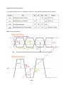
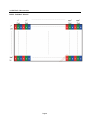
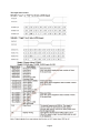
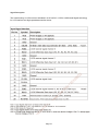
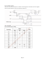
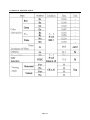
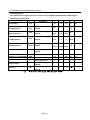
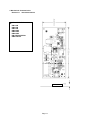
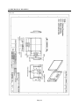
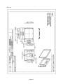
LITEMAX SLD/SLO1268 Sunlight Readable 12.1” LED B/L LCD User Manual (1st Edition 2011/10/18 ) All information is subject to change without notice. Approved by Checked by Prepared by LITEMAX Electronics Inc. 8F., No.137, Ln. 235, Baoqiao Rd., Xindian Dist., New Taipei City 23145, Taiwan Tel : 886-2-8919-1858 Fax: 886-2-8919-1300 Homepage: http://www.litemax.com Page 1 RECORD OF REVISION Version and Date Oct,18,2011 Page Old Description all New Description Initial Release Page 2 Remark Contents Contents............................................................................................................................................. 3 1.0 GENERAL DESCRIPTION ........................................................................................................... 4 1.1 FEATURES ............................................................................................................................ 4 1.2 GENERAL SPECIFICATIONS................................................................................................ 4 1.3 ABSOLUTE MAXIMUM RATINGS ......................................................................................... 4 2.0 Electrical characteristics ............................................................................................................ 6 3.0 SIGNAL Characteristic ................................................................................................................ 8 4.0 TIMING Characteristics............................................................................................................. 11 5.0 CONNECTOR and PIN ASSIGNMENT ...................................................................................... 13 6.0 OPTICAL SPECIFICATION ........................................................................................................ 14 7.0 LED DRIVING BOARD SPECIFICATIONS ................................................................................ 15 8.0 MECHANICAL DRAWING.......................................................................................................... 18 9.0 PRECAUTIONS .......................................................................................................................... 20 Page 3 1.0 GENERAL DESCRIPTION SLD/SLO1268 is 12.1” wide color TFT-LCD Display as active switching devices with 1,600nits LED backlight powered by Durapixel™ technology. This LCD display has a 12.1 inch diagonally measured active area with XGA resolutions (1024 horizontal by 768 vertical pixel array). Each pixel is divided into RED, GREEN, BLUE dots which are arranged in vertical stripe and this module can display 16.2M colors. 1.1 FEATURES Sunlight Readable LED Backlight XGA(1024x768) High Definition High Shock & Vibration Resistance Low Power Consumption High Uniformity Low EMI Noise Wide Dimming Wide Temperature(-30°C~-85°C) Life Expectancy 1.2 GENERAL SPECIFICATIONS Model No. Description Display Area (mm) Brightness Resolution Contrast Ratio Pixel Pitch (mm) Viewing Angle Display Colors Response Time (Typical) Power Consumption Dimensions (mm) Weight (Net) SLD1268 SLO1268 12.1” LCD Display, LED Backlight 1600nits,XGA(1024x768) 245.76(H) x 184.32(V) mm 1600 cd/m2 1024x768 (XGA) 700 : 1 0.24(H) x 0.24(V) +80°~‐80°(H), +80°~‐80°(V) 16.2M 35ms 17W 17W 272x205.4x36.2mm 293.6x205.6x36.7mm 1.0Kg 1.05Kg 1.3 ABSOLUTE MAXIMUM RATINGS ABSOLUTE RATINGS OF LCD Module Page 4 TFT LCD ENVIRONMENTAL Specification Note: Maximum Web-Bulb should be 39°C and no condensation Page 5 2.0 Electrical characteristics TFT LCD Module Power Specification Input power specifications are as following: Note: Measurement conditions: Page 6 Signal Electrical Characteristics Input signals shall be low or Hi-Z state when VDD is off. Each signal characteristics are as follows: Note: LVDS Signal Waveform Page 7 3.0 SIGNAL Characteristic PIXEL FORMAT IMAGE Page 8 The input data format: Page 9 Signal Description The module using a LVDS receiver embaded in AUO’s ASIC. LVDS is a differential signal technology for LCD interface and high-speed data transfer device. Page 10 4.0 TIMING Characteristics Input Timing Diagram Page 11 Power ON/OFF Sequence VDD power and LED on/off sequence is as follows. Interface signals are also shown in the chart. Signals from any system shall be Hi‐Z state or low level when VDD is off. Power On/Off Sequence Timing Page 12 5.0 CONNECTOR and PIN ASSIGNMENT Physical interface is described as for the connector on module. These connectors are capable of accommodating the following signals and will be following components. TFT LCD Module PIN ASSIGNMENT Page 13 6.0 OPTICAL SPECIFICATION Page 14 7.0 LED DRIVING BOARD SPECIFICATIONS 1.LED (Application) This specification is applied to LED converter unit for SLD/SLO1268(1600 nits) LED backlight 2 Operating Characteristics Item Symbol Input Voltage Vin Input Current (Low Brightness) VIN=Input Voltage, IinL Input Current (High Brightness) Vadj=5V MIN. TYP. MAX. 10 12 14 0.0 ----- ----- 0.93 0.77 0.66 0.0 ----- ----- Unit V Remark DC A VIN=Input Voltage, IinH Vadj=0V A VIN=Input Voltage, LED Current (Low Brightness) Conditions IoutL LED Current Vadj=5V Arms VIN=Input Voltage, A (High Brightness) IoutH Vadj=0V 0.423 Working Frequency Freq VIN=Input Voltage, 539.55 545 180 200 220 HZ 0.5 ----- 4.8 V 1.5 ----- 5 0.423 0.423 550.45 KHZ Vadj=0V PWM Frequency Brightness Control(PWM) ON/OFF Control Output Voltage Efficiency Freq Vadj Von/off VIN=Input Voltage Connection of Voltage V DC DC Vout Normal Operation VIN=Input Voltage, 20.249 20.246 20.246 V DC η Vadj=0V VIN=Input Voltage, 92.10 % Note 1 92.68 Vadj=0V Note 1:Efficiency=[(IoutH﹡Vout)/(IinH﹡Vin)] ﹡100%,Tolerance ±0.5% Page 15 92.68 3.Connector Socket 3-1. Input Connector: Input Connector J3(JST S8B-PH-SM3-TB or Compatible): PIN No Symbol Description 1 Vin DC+12V 2 Vin DC+12V 3 Vin DC+12V 4 GND Ground 5 GND Ground 6 GND Ground 7 Brightness 8 Control Brightness Control 5V~0V ON/OFF Control 0.8V(OFF) 2.0~5.0V(ON) 3-2 .Output Connector: J1,J2(JST S2B-EH or Compatible): PIN NO Symbol Description 1 Output LED High Voltage( + ) 2 Output LED Low Voltage ( - ) Page 16 4. Mechanical Characteristics Dimension: 70mm*30mm*5mm INPUT CONNECTOR J3: PIN1:VIN PIN2:VIN PIN3:VIN PIN4:GND PIN5:GND PIN6:GND PIN7:BRIGHTNESS PIN8:ON/OFF 5mm Page 17 8.0 MECHANICAL DRAWING SLD1268 Page 18 SLO1268 Page 19 9.0 PRECAUTIONS HANDLING PRECAUTIONS (1) The module should be assembled into the system firmly by using every mounting hole. Be careful not to twist or bend the module. (2) While assembling or installing modules, it can only be in the clean area. The dust and oil may cause electrical short or damage the polarizer. (3) Use fingerstalls or soft gloves in order to keep display clean during the incoming inspection and assembly process. (4) Do not press or scratch the surface harder than a HB pencil lead on the panel because the polarizer is very soft and easily scratched. (5) If the surface of the polarizer is dirty, please clean it by some absorbent cotton or soft cloth. Do not use Ketone type materials (ex. Acetone), Ethyl alcohol, Toluene, Ethyl acid or Methyl chloride. It might permanently damage the polarizer due to chemical reaction. (6) Wipe off water droplets or oil immediately. Staining and discoloration may occur if they left on panel for a long time. (7) If the liquid crystal material leaks from the panel, it should be kept away from the eyes or mouth. In case of contacting with hands, legs or clothes, it must be washed away thoroughly with soap. (8) Protect the module from static electricity, it may cause damage to the C-MOS Gate Array IC. (9) Do not disassemble the module. (10) Do not pull or fold the lamp wire. (11) Pins of I/F connector should not be touched directly with bare hands. STORAGE PRECAUTIONS (1) High temperature or humidity may reduce the performance of module. Please store LCD module within the specified storage conditions. (2) It is dangerous that moisture come into or contacted the LCD module, because the moisture may damage LCD module when it is operating. (3) It may reduce the display quality if the ambient temperature is lower than 10 ºC. For example, the response time will become slowly, and the starting voltage of lamp will be higher than the room temperature. OPERATION PRECAUTIONS (1) Do not pull the I/F connector in or out while the module is operating. (2) Always follow the correct power on/off sequence when LCD module is connecting and operating. This can prevent the CMOS LSI chips from damage during latch-up. Page 20