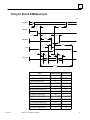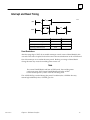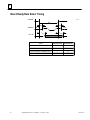
1
GE
Intelligent Platforms
ÎÎ
Programmable Control Products
Genius* I/O
µGENI Board
User’s Manual
GFK-0845A
March 2010
GFL-002
Warnings, Cautions, and Notes
as Used in this Publication
Warning
Warning notices are used in this publication to emphasize that hazardous voltages,
currents, temperatures, or other conditions that could cause personal injury exist in this
equipment or may be associated with its use.
In situations where inattention could cause either personal injury or damage to equipment,
a Warning notice is used.
Caution
Caution notices are used where equipment might be damaged if care is not taken.
Note:
Notes merely call attention to information that is especially significant to
understanding and operating the equipment.
This document is based on information available at the time of its publication. While efforts
have been made to be accurate, the information contained herein does not purport to cover all
details or variations in hardware or software, nor to provide for every possible contingency in
connection with installation, operation, or maintenance. Features may be described herein
which are not present in all hardware and software systems. GE Intelligent Platforms assumes
no obligation of notice to holders of this document with respect to changes subsequently made.
GE Intelligent Platforms makes no representation or warranty, expressed, implied, or statutory
with respect to, and assumes no responsibility for the accuracy, completeness, sufficiency, or
usefulness of the information contained herein. No warranties of merchantability or fitness for
purpose shall apply.
* indicates a trademark of GE Intelligent Platforms, Inc. and/or its affiliates. All other
trademarks are the property of their respective owners.
©Copyright 2010 GE Intelligent Platforms, Inc.
All Rights Reserved
Contact Information
If you purchased this product through an Authorized Channel Partner, please contact the seller
directly.
General Contact Information
Online technical support and
GlobalCare
http://www.ge-ip.com/support
1H2
Additional information
http://www.ge-ip.com/
3H
Solution Provider
[email protected]
4H
Technical Support
If you have technical problems that cannot be resolved with the information in this guide, please
contact us by telephone or email, or on the web at www.ge-ip.com/support
5H
Americas
Online Technical Support
www.ge-ip.com/support
6H7
Phone
1-800-433-2682
International Americas Direct Dial
1-780-420-2010 (if toll free 800 option is unavailable)
Technical Support Email
[email protected]
8H9
Customer Care Email
Primary language of support
[email protected]
10H
English
Europe, the Middle East, and Africa
Online Technical Support
www.ge-ip.com/support
12H3
Phone
+800-1-433-2682
EMEA Direct Dial
+352-26-722-780 (if toll free 800 option is unavailable or if
dialing from a mobile telephone)
Technical Support Email
[email protected]
14H5
Customer Care Email
Primary languages of support
[email protected]
16H7
English, French, German, Italian, Czech, Spanish
Asia Pacific
Online Technical Support
www.ge-ip.com/support
Phone
18H9
+86-400-820-8208
+86-21-3217-4826 (India, Indonesia, and Pakistan)
Technical Support Email
[email protected] (China)
20H1
[email protected] (Japan)
2H3
[email protected] (remaining Asia customers)
24H5
Customer Care Email
[email protected]
26H7
[email protected] (China)
28H
Preface
t
This book provides the information needed to integrate a Genius µGENI Network
Interface (µGENI) board in a user-developed microprocessor system. The reader should
be familiar with microprocessor system design and implementation, and with the
Genius I/O system.
Contents of this Manual
This book contains the following chapters:
Chapter 1. Introduction: gives board specifications, and describes µGENI’s capabilities.
Chapter 2. Hardware Interface: contains information about µGENI board hardware,
motherboard requirements, signals, and timing.
Chapter 3. Software Interface: describes the µGENI’s Shared RAM memory, which
handles all data transfer between µGENI and the host. Chapter 3 also summarizes
µGENI’s activities during startup, steady state operation, and device login.
Chapter 4. Setup: describes the area of Shared RAM where µGENI stores its Genius bus
setting and other setup data.
Chapter 5. Status: describes the portion of Shared RAM where µGENI stores its status
data.
Chapter 6. Interrupts: describes Interrupt conditions. Chapter 6 also explains how to
monitor Interrupt status, and how to enable or disable Interrupts from µGENI to the
host.
Chapter 7. Device Configuration: describes the table in Shared RAM where µGENI
stores information about devices on the bus. It also explains how µGENI obtains this
data.
Chapter 8. Device Inputs and Outputs: describes the area of Shared RAM which is used
for input and output data.
Chapter 9. I/O Table Lockout: explains how the host can request or relinquish lockout of
the I/O Tables in Shared RAM.
Chapter 10. Commands: explains how the host can send and receive datagrams, and
change µGENI configuration.
Chapter 11. Global Data: describes how µGENI can automatically exchange up to 128
bytes of Global Data with all other devices on the bus.
Chapter 12. Directed Control Data: explains how µGENI can direct or receive up to 128
bytes of data to/from any other bus controller.
Chapter 13. Memory Access Datagrams: explains how µGENI handles requests by other
devices to read or write host memory.
GFK-0845A
V
Preface
Chapter 14. Troubleshooting: suggests troubleshooting steps based on observation of
LEDS and the occurrence of bus errors.
Appendix A. General Macro Definitions: suggests simple macro definitions that might
be used for a C language interface to µGENI.
For More Information
Refer to the Genius I/O System User’s Manual (GEK-90486) for detailed information about
Genius I/O blocks, system communications, types of systems, and system planning.
We Welcome Your Comments and Suggestions
At GE Intelligent Platforms, we strive to produce quality technical documentation. After
you have used this manual, please take a few moments to complete and return the
Reader ’s Comment Card located on the next page.
Jeanne Grimsby
senior technical writer
vi
Genius I/O mGENI Board User’s Manual – October 1995
GFK-0845A
Contents
Chapter 1
Chapter 2
Chapter 3
Chapter 4
Chapter 5
GFK-0845A
Introduction . . . . . . . . . . . . . . . . . . . . . . . . . . . . . . . . . . . . . . . . . . . . . . .
1
Board Description . . . . . . . . . . . . . . . . . . . . . . . . . . . . . . . . . . . . . . . . . . . . . . . .
Board LEDs . . . . . . . . . . . . . . . . . . . . . . . . . . . . . . . . . . . . . . . . . . . . . . . . . . .
Genius Bus Setup Signals . . . . . . . . . . . . . . . . . . . . . . . . . . . . . . . . . . . . . . .
Board Specifications . . . . . . . . . . . . . . . . . . . . . . . . . . . . . . . . . . . . . . . . . . . .
Board Components . . . . . . . . . . . . . . . . . . . . . . . . . . . . . . . . . . . . . . . . . . . . . . .
Motherboard Requirements . . . . . . . . . . . . . . . . . . . . . . . . . . . . . . . . . . . . . . . .
Mounting . . . . . . . . . . . . . . . . . . . . . . . . . . . . . . . . . . . . . . . . . . . . . . . . . . . . .
Power Supply Requirements . . . . . . . . . . . . . . . . . . . . . . . . . . . . . . . . . . . .
Genius Setup Signals . . . . . . . . . . . . . . . . . . . . . . . . . . . . . . . . . . . . . . . . . . .
2
2
2
3
4
5
5
5
6
Hardware Interface . . . . . . . . . . . . . . . . . . . . . . . . . . . . . . . . . . . . . . . .
7
BusLoads/DriveCapability . . . . . . . . . . . . . . . . . . . . . . . . . . . . . . . . . . . . . . . .
Motherboard Wiring Requirements . . . . . . . . . . . . . . . . . . . . . . . . . . . . . . . . .
Signal Conditioning . . . . . . . . . . . . . . . . . . . . . . . . . . . . . . . . . . . . . . . . . . . .
Faceplate Markings . . . . . . . . . . . . . . . . . . . . . . . . . . . . . . . . . . . . . . . . . . . .
Hand–held Monitor Connector . . . . . . . . . . . . . . . . . . . . . . . . . . . . . . . . .
Bus Cable Selection . . . . . . . . . . . . . . . . . . . . . . . . . . . . . . . . . . . . . . . . . . . .
10 Volt Connector Signals . . . . . . . . . . . . . . . . . . . . . . . . . . . . . . . . . . . . . . . . . .
5 Volt Connector Signals . . . . . . . . . . . . . . . . . . . . . . . . . . . . . . . . . . . . . . . . . . .
Timing for Shared RAM Read Cycle . . . . . . . . . . . . . . . . . . . . . . . . . . . . . . . . .
Timing for Shared RAM Write Cycle . . . . . . . . . . . . . . . . . . . . . . . . . . . . . . . . .
Interrupt and Reset Timing . . . . . . . . . . . . . . . . . . . . . . . . . . . . . . . . . . . . . . . .
Board Ready/Data Select Timing . . . . . . . . . . . . . . . . . . . . . . . . . . . . . . . . . . . .
7
8
9
10
10
10
10
11
13
14
15
16
Software Interface . . . . . . . . . . . . . . . . . . . . . . . . . . . . . . . . . . . . . . . . .
17
Shared RAM Structure Variables . . . . . . . . . . . . . . . . . . . . . . . . . . . . . . . . . . . .
Interface Suggestions . . . . . . . . . . . . . . . . . . . . . . . . . . . . . . . . . . . . . . . . . . . . .
Startup Self–test . . . . . . . . . . . . . . . . . . . . . . . . . . . . . . . . . . . . . . . . . . . . . . . . .
Steady State Operation . . . . . . . . . . . . . . . . . . . . . . . . . . . . . . . . . . . . . . . . . . . .
Device Login and Log–out . . . . . . . . . . . . . . . . . . . . . . . . . . . . . . . . . . . . . . . .
18
19
21
22
23
Setup . . . . . . . . . . . . . . . . . . . . . . . . . . . . . . . . . . . . . . . . . . . . . . . . . . . . .
25
Example Variables . . . . . . . . . . . . . . . . . . . . . . . . . . . . . . . . . . . . . . . . . . . . . . . .
Changing the Setup Table . . . . . . . . . . . . . . . . . . . . . . . . . . . . . . . . . . . . . . . . . .
Read ID Requests . . . . . . . . . . . . . . . . . . . . . . . . . . . . . . . . . . . . . . . . . . . . . . . . .
26
26
26
Status . . . . . . . . . . . . . . . . . . . . . . . . . . . . . . . . . . . . . . . . . . . . . . . . . . . .
27
Software Revision Number . . . . . . . . . . . . . . . . . . . . . . . . . . . . . . . . . . . . . . . .
Board OK Status . . . . . . . . . . . . . . . . . . . . . . . . . . . . . . . . . . . . . . . . . . . . . . . . . .
Board Hardware Status . . . . . . . . . . . . . . . . . . . . . . . . . . . . . . . . . . . . . . . . . . .
Example Variables . . . . . . . . . . . . . . . . . . . . . . . . . . . . . . . . . . . . . . . . . . . . . . . .
Monitoring a Heartbeat . . . . . . . . . . . . . . . . . . . . . . . . . . . . . . . . . . . . . . . . . . .
27
27
28
29
30
Table of Contents
vii
Contents
Chapter 6
Chapter 7
Chapter 8
Chapter 9
Chapter 10
viii
Interrupts . . . . . . . . . . . . . . . . . . . . . . . . . . . . . . . . . . . . . . . . . . . . . . . . .
33
Example Variables . . . . . . . . . . . . . . . . . . . . . . . . . . . . . . . . . . . . . . . . . . . . . . . .
Interrupt Table . . . . . . . . . . . . . . . . . . . . . . . . . . . . . . . . . . . . . . . . . . . . . . . . . . .
Disable Interrupt Table . . . . . . . . . . . . . . . . . . . . . . . . . . . . . . . . . . . . . . . . . . . .
33
34
35
Device Configuration . . . . . . . . . . . . . . . . . . . . . . . . . . . . . . . . . . . . . . .
37
Device Configuration Changes . . . . . . . . . . . . . . . . . . . . . . . . . . . . . . . . . . . . .
Device Configuration Table . . . . . . . . . . . . . . . . . . . . . . . . . . . . . . . . . . . . . . . .
Example Variables . . . . . . . . . . . . . . . . . . . . . . . . . . . . . . . . . . . . . . . . . . . . . . . .
38
38
40
Device Inputs and Outputs . . . . . . . . . . . . . . . . . . . . . . . . . . . . . . . . . .
41
Example Variable . . . . . . . . . . . . . . . . . . . . . . . . . . . . . . . . . . . . . . . . . . . . . . . . .
I/OTable Structure . . . . . . . . . . . . . . . . . . . . . . . . . . . . . . . . . . . . . . . . . . . . . . . .
Input Table . . . . . . . . . . . . . . . . . . . . . . . . . . . . . . . . . . . . . . . . . . . . . . . . . . . . . .
Location of a Device’s Input Buffer . . . . . . . . . . . . . . . . . . . . . . . . . . . . . . .
Output Table . . . . . . . . . . . . . . . . . . . . . . . . . . . . . . . . . . . . . . . . . . . . . . . . . . . . .
41
42
43
43
45
I/O Table Lockout . . . . . . . . . . . . . . . . . . . . . . . . . . . . . . . . . . . . . . . . . .
47
Lockout Procedure . . . . . . . . . . . . . . . . . . . . . . . . . . . . . . . . . . . . . . . . . . . . . . . .
Example Algorithm . . . . . . . . . . . . . . . . . . . . . . . . . . . . . . . . . . . . . . . . . . . . . . .
47
48
Commands . . . . . . . . . . . . . . . . . . . . . . . . . . . . . . . . . . . . . . . . . . . . . . . .
49
Command Block . . . . . . . . . . . . . . . . . . . . . . . . . . . . . . . . . . . . . . . . . . . . . . . . . .
Status Byte . . . . . . . . . . . . . . . . . . . . . . . . . . . . . . . . . . . . . . . . . . . . . . . . . . . .
Command Byte Format . . . . . . . . . . . . . . . . . . . . . . . . . . . . . . . . . . . . . . . . .
Example Variables . . . . . . . . . . . . . . . . . . . . . . . . . . . . . . . . . . . . . . . . . . . . .
Example Macros . . . . . . . . . . . . . . . . . . . . . . . . . . . . . . . . . . . . . . . . . . . . . . .
Example Algorithms . . . . . . . . . . . . . . . . . . . . . . . . . . . . . . . . . . . . . . . . . . .
Read Datagram Command . . . . . . . . . . . . . . . . . . . . . . . . . . . . . . . . . . . . . . . . .
Procedure . . . . . . . . . . . . . . . . . . . . . . . . . . . . . . . . . . . . . . . . . . . . . . . . . . . .
Status Definitions . . . . . . . . . . . . . . . . . . . . . . . . . . . . . . . . . . . . . . . . . . . . . .
Example Variables . . . . . . . . . . . . . . . . . . . . . . . . . . . . . . . . . . . . . . . . . . . . .
Transmit Datagram Command . . . . . . . . . . . . . . . . . . . . . . . . . . . . . . . . . . . . .
Priority . . . . . . . . . . . . . . . . . . . . . . . . . . . . . . . . . . . . . . . . . . . . . . . . . . . . . . . . . .
Maximum Datagram Length . . . . . . . . . . . . . . . . . . . . . . . . . . . . . . . . . . . .
Procedure . . . . . . . . . . . . . . . . . . . . . . . . . . . . . . . . . . . . . . . . . . . . . . . . . . . .
Status Definitions Command Status . . . . . . . . . . . . . . . . . . . . . . . . . . . . . .
Example Variables . . . . . . . . . . . . . . . . . . . . . . . . . . . . . . . . . . . . . . . . . . . . .
Transmit Datagram with Reply Command . . . . . . . . . . . . . . . . . . . . . . . . . . .
Procedure . . . . . . . . . . . . . . . . . . . . . . . . . . . . . . . . . . . . . . . . . . . . . . . . . . . .
Status Definitions . . . . . . . . . . . . . . . . . . . . . . . . . . . . . . . . . . . . . . . . . . . . . .
Example Variables . . . . . . . . . . . . . . . . . . . . . . . . . . . . . . . . . . . . . . . . . . . . .
Configuration Change Command . . . . . . . . . . . . . . . . . . . . . . . . . . . . . . . . . . .
Procedure . . . . . . . . . . . . . . . . . . . . . . . . . . . . . . . . . . . . . . . . . . . . . . . . . . . .
Status Definitions . . . . . . . . . . . . . . . . . . . . . . . . . . . . . . . . . . . . . . . . . . . . . .
49
50
51
52
52
52
54
54
55
55
56
57
57
57
58
58
59
60
61
61
62
62
63
mGENI Board User’s Manual – October 1995
GFK-0845A
Contents
Chapter 11
Chapter 12
Chapter 13
Chapter 14
Appendix A
GFK-0845A
Global Data . . . . . . . . . . . . . . . . . . . . . . . . . . . . . . . . . . . . . . . . . . . . . . .
65
Table Lockout . . . . . . . . . . . . . . . . . . . . . . . . . . . . . . . . . . . . . . . . . . . . . . . . . . . .
65
Sending Global Data . . . . . . . . . . . . . . . . . . . . . . . . . . . . . . . . . . . . . . . . . . . . . .
66
Receiving Global Data . . . . . . . . . . . . . . . . . . . . . . . . . . . . . . . . . . . . . . . . . . . . .
66
Timing Considerations . . . . . . . . . . . . . . . . . . . . . . . . . . . . . . . . . . . . . . . . . . . .
66
Directed Control Data . . . . . . . . . . . . . . . . . . . . . . . . . . . . . . . . . . . . . .
67
Sending Directed Control Data . . . . . . . . . . . . . . . . . . . . . . . . . . . . . . . . . . . . .
68
Receiving Directed Control Data . . . . . . . . . . . . . . . . . . . . . . . . . . . . . . . . . . . .
68
Timing Considerations . . . . . . . . . . . . . . . . . . . . . . . . . . . . . . . . . . . . . . . . . . . .
68
Table Lockout . . . . . . . . . . . . . . . . . . . . . . . . . . . . . . . . . . . . . . . . . . . . . . . . . . . .
69
Using Global Data and Directed Control Data . . . . . . . . . . . . . . . . . . . . . . . . .
69
Memory Access Datagrams . . . . . . . . . . . . . . . . . . . . . . . . . . . . . . . . .
71
Sending Memory Access Datagrams . . . . . . . . . . . . . . . . . . . . . . . . . . . . . . . . .
71
Receiving Memory Access Datagrams . . . . . . . . . . . . . . . . . . . . . . . . . . . . . . .
71
Handling the Request Queue . . . . . . . . . . . . . . . . . . . . . . . . . . . . . . . . . . . . . .
72
Host Responses to Memory Access Datagrams . . . . . . . . . . . . . . . . . . . . . . . .
73
Request Queue Buffers and Auxiliary Request Queue Buffers . . . . . . . . . . .
74
Request Queue Buffer Format . . . . . . . . . . . . . . . . . . . . . . . . . . . . . . . . . . .
74
Auxiliary Request Queue Buffer Format . . . . . . . . . . . . . . . . . . . . . . . . . . .
74
Header Bytes and Data Length . . . . . . . . . . . . . . . . . . . . . . . . . . . . . . . . . .
74
Status Byte . . . . . . . . . . . . . . . . . . . . . . . . . . . . . . . . . . . . . . . . . . . . . . . . . . . .
75
Example Variables for Request Queue Operations . . . . . . . . . . . . . . . . . .
75
Troubleshooting . . . . . . . . . . . . . . . . . . . . . . . . . . . . . . . . . . . . . . . . . . .
77
Board LEDs . . . . . . . . . . . . . . . . . . . . . . . . . . . . . . . . . . . . . . . . . . . . . . . . . . . . . .
77
Troubleshooting Steps . . . . . . . . . . . . . . . . . . . . . . . . . . . . . . . . . . . . . . . . . . . . .
78
General Macro Definitions . . . . . . . . . . . . . . . . . . . . . . . . . . . . . . . . . .
79
Table of Contents
ix
Contents
Chapter 6
Chapter 7
Chapter 8
Chapter 9
Chapter 10
x
Interrupts . . . . . . . . . . . . . . . . . . . . . . . . . . . . . . . . . . . . . . . . . . . . . . . . .
33
Example Variables . . . . . . . . . . . . . . . . . . . . . . . . . . . . . . . . . . . . . . . . . . . . . . . .
Interrupt Table . . . . . . . . . . . . . . . . . . . . . . . . . . . . . . . . . . . . . . . . . . . . . . . . . . .
Disable Interrupt Table . . . . . . . . . . . . . . . . . . . . . . . . . . . . . . . . . . . . . . . . . . . .
33
34
35
Device Configuration . . . . . . . . . . . . . . . . . . . . . . . . . . . . . . . . . . . . . . .
37
Device Configuration Changes . . . . . . . . . . . . . . . . . . . . . . . . . . . . . . . . . . . . .
Device Configuration Table . . . . . . . . . . . . . . . . . . . . . . . . . . . . . . . . . . . . . . . .
Example Variables . . . . . . . . . . . . . . . . . . . . . . . . . . . . . . . . . . . . . . . . . . . . . . . .
38
38
40
Device Inputs and Outputs . . . . . . . . . . . . . . . . . . . . . . . . . . . . . . . . . .
41
Example Variable . . . . . . . . . . . . . . . . . . . . . . . . . . . . . . . . . . . . . . . . . . . . . . . . .
I/OTable Structure . . . . . . . . . . . . . . . . . . . . . . . . . . . . . . . . . . . . . . . . . . . . . . . .
Input Table . . . . . . . . . . . . . . . . . . . . . . . . . . . . . . . . . . . . . . . . . . . . . . . . . . . . . .
Location of a Device’s Input Buffer . . . . . . . . . . . . . . . . . . . . . . . . . . . . . . .
Output Table . . . . . . . . . . . . . . . . . . . . . . . . . . . . . . . . . . . . . . . . . . . . . . . . . . . . .
41
42
43
43
45
I/O Table Lockout . . . . . . . . . . . . . . . . . . . . . . . . . . . . . . . . . . . . . . . . . .
47
Lockout Procedure . . . . . . . . . . . . . . . . . . . . . . . . . . . . . . . . . . . . . . . . . . . . . . . .
Example Algorithm . . . . . . . . . . . . . . . . . . . . . . . . . . . . . . . . . . . . . . . . . . . . . . .
47
48
Commands . . . . . . . . . . . . . . . . . . . . . . . . . . . . . . . . . . . . . . . . . . . . . . . .
49
Command Block . . . . . . . . . . . . . . . . . . . . . . . . . . . . . . . . . . . . . . . . . . . . . . . . . .
Status Byte . . . . . . . . . . . . . . . . . . . . . . . . . . . . . . . . . . . . . . . . . . . . . . . . . . . .
Command Byte Format . . . . . . . . . . . . . . . . . . . . . . . . . . . . . . . . . . . . . . . . .
Example Variables . . . . . . . . . . . . . . . . . . . . . . . . . . . . . . . . . . . . . . . . . . . . .
Example Macros . . . . . . . . . . . . . . . . . . . . . . . . . . . . . . . . . . . . . . . . . . . . . . .
Example Algorithms . . . . . . . . . . . . . . . . . . . . . . . . . . . . . . . . . . . . . . . . . . .
Read Datagram Command . . . . . . . . . . . . . . . . . . . . . . . . . . . . . . . . . . . . . . . . .
Procedure . . . . . . . . . . . . . . . . . . . . . . . . . . . . . . . . . . . . . . . . . . . . . . . . . . . .
Status Definitions . . . . . . . . . . . . . . . . . . . . . . . . . . . . . . . . . . . . . . . . . . . . . .
Example Variables . . . . . . . . . . . . . . . . . . . . . . . . . . . . . . . . . . . . . . . . . . . . .
Transmit Datagram Command . . . . . . . . . . . . . . . . . . . . . . . . . . . . . . . . . . . . .
Priority . . . . . . . . . . . . . . . . . . . . . . . . . . . . . . . . . . . . . . . . . . . . . . . . . . . . . . . . . .
Maximum Datagram Length . . . . . . . . . . . . . . . . . . . . . . . . . . . . . . . . . . . .
Procedure . . . . . . . . . . . . . . . . . . . . . . . . . . . . . . . . . . . . . . . . . . . . . . . . . . . .
Status Definitions Command Status . . . . . . . . . . . . . . . . . . . . . . . . . . . . . .
Example Variables . . . . . . . . . . . . . . . . . . . . . . . . . . . . . . . . . . . . . . . . . . . . .
Transmit Datagram with Reply Command . . . . . . . . . . . . . . . . . . . . . . . . . . .
Procedure . . . . . . . . . . . . . . . . . . . . . . . . . . . . . . . . . . . . . . . . . . . . . . . . . . . .
Status Definitions . . . . . . . . . . . . . . . . . . . . . . . . . . . . . . . . . . . . . . . . . . . . . .
Example Variables . . . . . . . . . . . . . . . . . . . . . . . . . . . . . . . . . . . . . . . . . . . . .
Configuration Change Command . . . . . . . . . . . . . . . . . . . . . . . . . . . . . . . . . . .
Procedure . . . . . . . . . . . . . . . . . . . . . . . . . . . . . . . . . . . . . . . . . . . . . . . . . . . .
Status Definitions . . . . . . . . . . . . . . . . . . . . . . . . . . . . . . . . . . . . . . . . . . . . . .
49
50
51
52
52
52
54
54
55
55
56
57
57
57
58
58
59
60
61
61
62
62
63
mGENI Board User’s Manual – October 1995
GFK-0845A
Contents
Chapter 1
Chapter 2
Chapter 3
Chapter 4
Chapter 5
GFK-0845A
Introduction . . . . . . . . . . . . . . . . . . . . . . . . . . . . . . . . . . . . . . . . . . . . . . .
1
Board Description . . . . . . . . . . . . . . . . . . . . . . . . . . . . . . . . . . . . . . . . . . . . . . . .
Board LEDs . . . . . . . . . . . . . . . . . . . . . . . . . . . . . . . . . . . . . . . . . . . . . . . . . . .
Genius Bus Setup Signals . . . . . . . . . . . . . . . . . . . . . . . . . . . . . . . . . . . . . . .
Board Specifications . . . . . . . . . . . . . . . . . . . . . . . . . . . . . . . . . . . . . . . . . . . .
Board Components . . . . . . . . . . . . . . . . . . . . . . . . . . . . . . . . . . . . . . . . . . . . . . .
Motherboard Requirements . . . . . . . . . . . . . . . . . . . . . . . . . . . . . . . . . . . . . . . .
Mounting . . . . . . . . . . . . . . . . . . . . . . . . . . . . . . . . . . . . . . . . . . . . . . . . . . . . .
Power Supply Requirements . . . . . . . . . . . . . . . . . . . . . . . . . . . . . . . . . . . .
Genius Setup Signals . . . . . . . . . . . . . . . . . . . . . . . . . . . . . . . . . . . . . . . . . . .
2
2
2
3
4
5
5
5
6
Hardware Interface . . . . . . . . . . . . . . . . . . . . . . . . . . . . . . . . . . . . . . . .
7
BusLoads/DriveCapability . . . . . . . . . . . . . . . . . . . . . . . . . . . . . . . . . . . . . . . .
Motherboard Wiring Requirements . . . . . . . . . . . . . . . . . . . . . . . . . . . . . . . . .
Signal Conditioning . . . . . . . . . . . . . . . . . . . . . . . . . . . . . . . . . . . . . . . . . . . .
Faceplate Markings . . . . . . . . . . . . . . . . . . . . . . . . . . . . . . . . . . . . . . . . . . . .
Hand–held Monitor Connector . . . . . . . . . . . . . . . . . . . . . . . . . . . . . . . . .
Bus Cable Selection . . . . . . . . . . . . . . . . . . . . . . . . . . . . . . . . . . . . . . . . . . . .
10 Volt Connector Signals . . . . . . . . . . . . . . . . . . . . . . . . . . . . . . . . . . . . . . . . . .
5 Volt Connector Signals . . . . . . . . . . . . . . . . . . . . . . . . . . . . . . . . . . . . . . . . . . .
Timing for Shared RAM Read Cycle . . . . . . . . . . . . . . . . . . . . . . . . . . . . . . . . .
Timing for Shared RAM Write Cycle . . . . . . . . . . . . . . . . . . . . . . . . . . . . . . . . .
Interrupt and Reset Timing . . . . . . . . . . . . . . . . . . . . . . . . . . . . . . . . . . . . . . . .
Board Ready/Data Select Timing . . . . . . . . . . . . . . . . . . . . . . . . . . . . . . . . . . . .
7
8
9
10
10
10
10
11
13
14
15
16
Software Interface . . . . . . . . . . . . . . . . . . . . . . . . . . . . . . . . . . . . . . . . .
17
Shared RAM Structure Variables . . . . . . . . . . . . . . . . . . . . . . . . . . . . . . . . . . . .
Interface Suggestions . . . . . . . . . . . . . . . . . . . . . . . . . . . . . . . . . . . . . . . . . . . . .
Startup Self–test . . . . . . . . . . . . . . . . . . . . . . . . . . . . . . . . . . . . . . . . . . . . . . . . .
Steady State Operation . . . . . . . . . . . . . . . . . . . . . . . . . . . . . . . . . . . . . . . . . . . .
Device Login and Log–out . . . . . . . . . . . . . . . . . . . . . . . . . . . . . . . . . . . . . . . .
18
19
21
22
23
Setup . . . . . . . . . . . . . . . . . . . . . . . . . . . . . . . . . . . . . . . . . . . . . . . . . . . . .
25
Example Variables . . . . . . . . . . . . . . . . . . . . . . . . . . . . . . . . . . . . . . . . . . . . . . . .
Changing the Setup Table . . . . . . . . . . . . . . . . . . . . . . . . . . . . . . . . . . . . . . . . . .
Read ID Requests . . . . . . . . . . . . . . . . . . . . . . . . . . . . . . . . . . . . . . . . . . . . . . . . .
26
26
26
Status . . . . . . . . . . . . . . . . . . . . . . . . . . . . . . . . . . . . . . . . . . . . . . . . . . . .
27
Software Revision Number . . . . . . . . . . . . . . . . . . . . . . . . . . . . . . . . . . . . . . . .
Board OK Status . . . . . . . . . . . . . . . . . . . . . . . . . . . . . . . . . . . . . . . . . . . . . . . . . .
Board Hardware Status . . . . . . . . . . . . . . . . . . . . . . . . . . . . . . . . . . . . . . . . . . .
Example Variables . . . . . . . . . . . . . . . . . . . . . . . . . . . . . . . . . . . . . . . . . . . . . . . .
Monitoring a Heartbeat . . . . . . . . . . . . . . . . . . . . . . . . . . . . . . . . . . . . . . . . . . .
27
27
28
29
30
Table of Contents
xi
1
Board Specifications
Electrical:
Inrush at Powerup
Power Requirements
BusLoading
Bus Drive Capability
Mechanical
GENI Board Dimensions
Environmental:
Operating:
Ambient Temperature at board
Humidity
Altitude
Vibration
Shock
Non–operating:
Ambient Temperature at board
Humidity
Altitude
Vibration
Shock
420mA,300µS
5 volts DC +/–10%,
470mA bus activity,
230mAidle
1 LS TTL load per input line
4 LS TTL loads per output line
Height at tallest component: top, .465 inches ( 11.811 mm)
bottom, .16 inches ( 4.064 mm)
Width: 3.3 inches (83.82 mm)
Depth: 4.5 inches (114.3 mm)
Board thickness: 0.063 inch (1.60 mm)
0C to +85 C, 32F to + 185F
5% to 95% non–condensing
10,000 feet
0.2 inch displacement 5 to 10 Hz
1 G 10 to 200 Hz
15 G. 10mS duration per MIL–STD 810C, method 516.2
–40C to +85 C, –40F to +185F
5% to 95% non–condensing
40,000 feet
0.2 inch displacement 5 to 10 Hz
1G 10 to 200 Hz
Board packed in shipping container:
15 G, 10mS duration per MIL–STD 810C, method 516.2
Ordering Information
Description
µGENI Board
32K x 8 EPROM
HHM Connector
Genius I/O System User’s Manuals
GFK-0845A
Chapter 1 Introduction
Catalog Number
IC660ELB912
44A723394–000
44A723293–001
GEK–90486
3
1
Board Components
Principal components of the µGENI board are:
4
6303 microprocessor
The serial interface microprocessor. It writes messages to
transmit buffers in the MIT chip.
MIT chip
The MIT chip handles the hardware interface to the bus. It
also provides many support functions such as CRC generation, error checking, a watchdog timer function, chip select,
LED drivers, and processor clock signals.
Transmit/receive
circuit
A circuit that interfaces the MIT transmit and receive signal
levels to bus signal levels.
Transformer
The transformer isolates the µGENI board circuitry from the
bus cable.
Dual port RAM
Dual port RAM is where the serial interface microprocessor
(6303) and the µGENI manager microprocessor (64180) exchange data. Dual port RAM removes timing skews between
the two processors, which are running two separate, asynchronous systems. Dual Port RAM is controlled by a GAL, which
arbitrates memory requests on a byte–by–byte basis, allowing the 6303 and the 64180 equal access.
64180 Microprocessor
This microprocessor transfers data between µGENI’s Shared
RAM and the serial interface microprocessor (6303), through
dual port RAM. The 64180 microprocessor has 8K bytes of
RAM for its exclusive use.
Shared RAM
Shared RAM is the host’s interface to µGENI. It provides 16K
bytes of storage space for I/O tables, configuration data, diagnostic data, and background message queues. Shared RAM
can be accessed by either µGENI or the host without loss of
data. There is no need for software arbitration. Shared RAM
looks like a pure RAM device to both systems. The GAL arbitrates Shared RAM memory requests on a byte–by–byte basis and allows the host and bus controller equal access to any
byte of Shared RAM without loss of data.
µGENI Board User’s Manual – October 1995
GFK-0845A
1
Shared RAM Address
Comparator
The Shared RAM Address Comparator causes a 64180 microprocessor interrupt when the host’s Write line is true and the
current Shared RAM address matches a specific interrupt
(command) byte address. The interrupt is latched until the
64810’s Read line is true and the current Shared RAM address
matches the specific interrupt (Command) byte address. Thus,
an interrupt occurs when the host writes to the command
byte and is cleared when the 64180 reads the command byte.
This circuit is implemented in a single array logic device (GAL)
which allows the address of the interrupt bytes to be reprogrammed during redevelopment, and provides the capability
for latching and clearing the interrupt.
Motherboard Requirements
The motherboard must provide the following minimum support:
H
H
H
H
H
+5V power connection with appropriate ground connections.
Powerup Reset pulse to the µGENI board.
Male 50-pin connector for signal and power signals to µGENI. Male 10-pin connector
for additional power and ground. Recommended mating connectors are available
from AMP, DuPont, Samtec, and Elco. 0.02” (0.508mm) square gold-plated pins
should be used.
Terminal block and optional D subminiature connector to the bus.
HHM connector (D subminiature connector) with HHM Present signal.
Mounting
The µGENI board is designed to be mounted to the motherboard, using spacers, via its
four corner holes. These holes accept plastic PCB supports (Richo Plastics or equivalent),
or screws or standoffs.
DO NOT
H
H
H
Mount the board where airflow across the board is obstructed.
Mount the board nearer than 1/8” (.125”) to any other boards or rack components.
Use adhesives or conformal coatings on any part of the board.
Power Supply Requirements
The µGENI board requires a 5 volt DC source for logic power. Supply voltage should not
vary more than 10% above or below nominal (below 4.5 VDC or above 5.5 VDC).
GFK-0845A
Chapter 1 Introduction
5
1
Genius Setup Signals
The Genius Setup signals P6(0) to P6(7) must be driven prior to bringing the mGENI
board out of reset on powerup. The eight signals determine: the baud rate, the status of
the output disable bytes during initialization, and the Device Number of the µGENI
board. The signals could be driven with DIP switches or latches, for example. Each signal
has a 10K pullup to set the default values.
Genius Setup Signal Assignments
7
6
5
4
3
2
1
46203
0
Device Number
Baud Rate:
00 = 153.6 Kbaud extended (8 bit skip time)
01 = 38.4 Kbaud (8 bit skip time)
10 = 76.8 Kbaud (8 bit skip time)
11 = 153.6 Kbaud standard (4 bit skip time)
Default Outputs Disable
0 = Outputs enabled at startup
1 = Outputs disabled at startup
Baud Rate
All devices on a bus must use the same baud rate: 153.6 Kbaud standard, 153.6 Kbaud extended, 76.8 Kbaud, or 38.4 Kbaud. The default is
153.6 Kbaud standard. Baud rate must be selected on the basis of cable
type, and other factors determined by the application.
Device Number
Each device connected to the Genius bus must have a unique Device
Number assigned .This number represents the module’s serial bus address. The default Device Number set with pullups on the setup signals
on the µGENI module is 31.
Each Genius communications bus can serve up to 32 devices, which are
identified by Device Numbers from 0 to 31. A module’s Device Number represents its place in the communications sequence on the bus.
By convention, certain numbers are associated with particular types of
devices. For example, Device Number 0 is normally used for a Genius
Hand–held Monitor. The Series 90–70 PLC and the Series Six PLC use
Device Numbers 30 and 31 for bus controllers in a backup (redundancy) type of system. Be sure that the Device Number assigned to the
µGENI bus controller is both unique and appropriate for the system.
Outputs
Enabled/Disabled
Disabling Outputs means preventing the transmission of outputs to all
devices on the bus when the µGENI bus controller is powered up. This
prevents incorrect operation of the outputs at powerup. The default is
for outputs to be disabled. To enable outputs, drive signal P6(7 ) to 0.
Changing the Genius Setup SIgnals
The mGENI reads these signals at powerup; if any signal is changed, it will be ignored
until the next time µGENI is powered up.
6
µGENI Board User’s Manual – October 1995
GFK-0845A
Chapter
2
2 Hardware Interface
section level 1 1
figure bi level 1
table_big level 1
Signal connection between µGENI and the motherboard is provided via a 50-pin female
connector and a 10-pin female connector.
The µGENI board’s interface signals are directly compatible with those of the IBM PC
backplane. Hosts with significant variances from the IBM PC backplane may require
motherboard translation circuitry.
46204
Data Bus (8)
Host
Motherboard
Address Bus (14)
A0 to A13
GENI Select
/GENSEL
Read
/RD
Write
/WR
Ready
/INT
Genius Setup
P6(0) to P6(7)
Reset
/RST
Status
/GENI OK
Status
/Comm OK
Genius Net (2)
µGENI
/GENRDY
Host Interrupt
HHM Present
Hand-held
Monitor
D0 to D7
Mono
X1, X2
Genius
Bus
Bus Loads/Drive Capability
All input lines to the µGENI present no more than one standard LSTTL load to the host
interface connector. All output lines from the µGENI except the /INT and /µGENI OK
lines are tri-state outputs. The /INT line is an open–collector output that can be
wired–ORed to a single interrupt input. The/µGENI OK and /COMM OK lines are
low–tr ue open-collector type outputs with built-in current-limiting to 5mA suitable for
driving LEDs directly.
GFK-0845A
7
2
Motherboard Wiring Requirements
1
2
Terminal
Connector
3
4
46205
X1
5
X2
9
SHD
4
MONO
ASHD
+5V
5VR
C1
Z1
49
50
HHM
Connector
F1
1
F2
6
Z2
34
µGENI Connector PL1
X1, X2, SHD, and ASHD must be 1/16 inch from all other signals on the motherboard.
MONO and 5VR must be 1/16 inch from all other signals on the motherboard up to the
high voltage suppressors, at which point, they may be grouped with the other
motherboard 5 volt signals.
X1, X2, SHD, and ASHD must be connected to a terminal connector on the motherboard.
The ASHD input, which connects to the bus shield, should be connected to earth ground
on the motherboard.
The µGENI contains high-speed switching devices that require good 0C and 5V
connection between the motherboard and the µGENI to minimize ground bounce
between the two boards, which could affect the quality of signals to/from the µGENI.
The µGENI is a multilayer board with 1oz 5V and 1oz 0V power planes. It is designed to
limit ground bounce on the board itself. Care must be taken in routing 0V and 5V to both
the 50-pin connector and the 10-pin connector.
The following illustration shows routing for the 0V and 5V pins on the connector with a
two-layer board.
46238
Two-Layer Motherboard
5V
0V
Due to the normal thermal relief patterns on power planes with 2mm center connector,
additional 0V and 5V connections are required on the outer signal layers for all 0V and
5V pins.
8
µGENI Board User’s Manual – October 1995
GFK-0845A
2
The following illustration represents routing for the 0V and 5V pins on a multilayer
motherboard with a 2mm connector.
46239
Multi-Layer Motherboard
Runs on
outer layer
Vias to 0V
or 5V
The runs into the 2mm center connector pin pads should be the full width of the pad,
typically .05” (1.27mm) to provide the lowest impedance path possible. Also, the length
of the 0.02” square posts from the motherboard to the µGENI should be as short as
possible to provide the lowest inductance path.
The µGENI utilizes ACT technology for driving the data lines and address lines shared
with the motherboard to provide faster switching speeds and more load-driving
capacity. Fanout and run length on the data lines and address lines must be limited to
avoid transmission line effects with the ACT technology. The suggested number of
buffering gates on the data lines is two (2) maximum. Pullup resistors should be avoided
on the data lines and address lines to limit the current required by the µGENI to drive
these signals low. Any buffering devices should be located as close as possible to the
respective µGENI connector pins. The preferred run length to a buffering device for the
data signals is 2”, with a maximum of 4” from the PL1 pins 35–42.
The/GENRDY signal is open collector to accommodate a wider range of
microprocessors; therefore, a pullup or pulldown resistor is required on the
motherboard.
The electromagnetic compatibility of the µGENI is determined by the grounding system
of the motherboard. The Genius connector on the motherboard should provide a shield
input (SHD) and a shield output (ASHD). The shield output must be connected directly
to earth ground. Special care should be taken on the motherboard when routing the
earth ground signal to minimize coupling with other signals and to provide the lowest
impedance path possible (0.1” earth ground run is suggested).
When routing circuitry under a µGENI daughterboard, care should be taken not to route
noisy signals under the µGENI. Some examples of noisy signals would be high speed
clocks with fast edges, driving signals with inductive kickback, and power supply
switchers.
Signal Conditioning
The MONO line should be protected from the accidental application of 120 VAC by
adding over–voltage protection devices on the motherboard. These devices should
shunt to ground any excess currents developed from high voltage devices applied to
either pin 1 or pin 6 of the HHM connector. Recommended devices are transient
suppressors with a breakdown voltage of 7.5 volts.
1.
1N6268A – Motorola and other vendors
2.
TZV7.5A – Semicon
The capacitor (“C1” in the illustration above) is recommended to shunt any AC noise
present on the bus shield. It should be a 0.1 µfarad ceramic 100 volt, 20% capacitor.
GFK–0845A
Chapter 2 Hardware Interface
9
2
Faceplate Markings
If a faceplate is used for the combined motherboard/daughterboard (referred to in this
book as the µGENI bus controller), it should provide the following names for the signals
on the external bus connector:
X1
SERIAL 1
X2
SERIAL 2
SHD
SHIELD IN
ASGD
SHIELD OUT
Hand–held Monitor Connector
The Hand–held Monitor connector should be a DE–9P subminiature male connector
capable of accepting two 4–40 threaded screws. The HHM mounting kit (part number
IC660MPH509) contains a D-connector, dress plates, and screw lock assembly. The dress
plate is mounted on the front of the D connector and held in place by two locking screws.
The unused pins on the D connector should remain unconnected in order to maintain
isolation between the X1, X2, SHD lines, and the MONO and 5VR lines.
Pin
Orientation
5
1
Hand-held
Monitor
Connector
Mating
Connector
ÎÎ
9
6
ÎÎ
46206
Î
ÎÎ
Î
ÎÎ
Î
ÎÎ
ÎÎ
Î
ÎÎ
ÎÎ
Î
Î
Bus Cable Selection
The type of bus cable used will depend upon the application requirements. The Genius
I/O System User’s Manual gives guidelines for bus cable selection.
10 Volt Connector Signals
The 50–pin connector provides the following Genius bus signals:
PIN
FUNCTION
50
X1
49
X2
48
NC
47
NC
46
NC
45
NC
X1 and X2 are differential signals that carry Genius bus data; they must be connected to
a terminal connector on the host motherboard.
10
µGENI Board User’s Manual – October 1995
GFK-0845A
2
5 Volt Connector Signals
The 10-pin connector provides the following 0-volt and 5-volt signals:
PIN
FUNCTION
PIN
FUNCTION
1
3
5
7
9
5V
5V
5V
5V
5V
2
4
6
8
10
0V
0V
0V
0V
0V
The 50–pin connector provides the following 5–volt signals:
GFK–0845A
PIN
FUNCTION
PIN
FUNCTION0V
1
2
3
4
5
6
7
8
9
10
11
12
13
14
15
16
17
18
19
20
21
22
0V
+5V
0V
+5V
A0
A1
A2
A3
A4
A5
A6
A7
A8
A9
A10
A11
A12
A13
P6(7)
P6(6)
P6(5)
P6(4)
23
24
25
26
27
28
29
30
31
32
33
34
35
36
37
38
39
40
41
42
43
44
P6(3)
P6(2)
P6(1)
P6(0)
NC
/RST
/INT
/RD
/WR
/GENSEL
/GENRDY
MONO
D0
D1
D2
D3
D4
D5
D6
D7
/GENIOK
/COMMOK
Chapter 2 Hardware Interface
11
2
Signals on the 50–pin connector are described in the following table.
Signal Type
Signal
Name
Description
Data
Signals
D0–D7
The eight data lines are bi–directional. They are used to transfer data
in the µGENI board’s Shared RAM to/from an 8–bit microprocessor–
type data bus. These lines enter the high– impedance state when
/RST is low or /GENSEL is high. Tristate output.
Address
Signals
A0–A13
Fourteen consecutive address lines which designate an address in
Shared RAM to be written or read.
Control
Signals
/WR
The Write strobe input to the µGENI indicates that data on D0–D7 is
valid and should be written from the host interface bus to Shared
RAM.
/RD
Read strobe line; The ReaD input to the µGENI is used during a host
CPU read cycle. It enables data transfer from Shared RAM to the host
interface bus.
/RST
ReSeT initializes the µGENI board when held low. It must be held low
during powerup and for a minimum of 20 milliseconds after all power
supplies are in tolerance. All µGENI output signals are held inactive
during reset.
/GENSEL
GENi SELect is use by the host to request access to Shared RAM. All
output signals from µGENI are held inactive and data cannot be written into Shared RAM when this signal is high.
/GENRDY
GENi ReaDY is an output from the µGENI to the host motherboard,
which tells the host to complete its memory access cycle. It is functionally identical to a ’WAIT’ signal from a slow memory device. The
host system should use this signal to introduce WAIT states if necessary during a µGENI Shared RAM access. /GENRDY falls low until
the low to high transitionof/RDor/WR. A high to low transition of
/GENRDY means that the host can stop inserting wait states (ending
its read or write cycle).
Interrupt
Signal
/INT
INT is an open–collector output that tells the host an event occurred
whenever it goes low (it pulses low for 5.44 µseconds). Provision
must be made for the host to remember that this pulse occurred.
Conditions that may cause an interrupt can be selected and monitored through the Shared RAM interface.
Status
Signals
MONO
When the HHM MONitOr (MONO) signal is high, a Hand– held
Monitor is attached to the HHM connector on the motherboard.
/µGENI OK
Reflects the µGENI OK LED output. Low when µGENI is running
normally. High when a hardware error has been detected. This line is
internally current–limited to 5mA. It can directly drive an LED or be
used as a logic signal.
COMM OK
A low /COMM OK output indicates no communicationserrors on the
bus. COMM OK is current limited and can directly drive an LED or
can be used as a logic signal.
5 Volt
5 volt +/–10% power supply input.
0 Volt
Logic ground input.
Bus Signals
X1 and X2
Differential signals that carry Genius bus data.
Genius Setup P6(0) to P6(7) Genius bus setup signals.
12
µGENI Board User’s Manual – October 1995
GFK-0845A
2
Timing for Shared RAM Read Cycle
46207
Address Valid
A0 to A13
tah
tas
/GENSEL
tsels
t rdy
trdyd
/GENRDY
trdh
trdr
tdv
/RD
tdlz
tdh
tdu
D0 to D7
tdhz
Data Valid
trdcyc
Item
Minimum nS
Maximum nS
Read Cycle Time (trdcyc)
500
–
Address Setup Time (tas)
0
–
Address Hold Time (tah)
0
–
µGENI Select Setup Time (tsels)
0
–
319
848
Ready Hold After Read (trdy)
5
31
Read Hold After Ready (trdh)
0
–
Read Recovery Time (trdr)
182
–
Data Time to Low Z (tdlz)
14
609
Data Undefined Time (tdu)
–
84
134
–
Data Hold Time (tdh)
3
14
Data Time to High Z (tdhz)
2
38
µGENI Ready Delay (trdyd)
Data Valid Before Ready (tdv)
GFK–0845A
Chapter 2 Hardware Interface
13
2
Timing for Shared RAM Write Cycle
46208
Address Valid
A0 to A13
tah
tas
/GENSEL
tsels
t rdy
trdyd
/GENRDY
twrh
twrr
/WR
tds
D0 to D7
tdh
Data Valid
twrcyc
Item
Minimum nS
Maximum nS
Write Cycle Time (twrcyc)
500
–
Address Setup Time (tas)
0
–
Address Hold Time (tah)
0
–
µGENI Select Setup Time (tsels)
0
–
319
848
Ready Hold After Write (trdy)
5
31
Write Hold After Ready (twrh)
0
–
182
–
Data Setup Time (tds)
0
–
Data Hold Time (tdh)
0
–
µGENI Ready Delay (trdyd)
Write Recovery Time (twrr)
14
µGENI Board User’s Manual – October 1995
GFK-0845A
2
Interrupt and Reset Timing
46209
tintp
/INT
tprst
trst
/RST
Item
Minimum
Maximum
/INTPulse Width (tintp)
5.44µS
–
Powerup/RSTPulse (tprst)
20mS
–
Operating/RSTPulse (trst)
10µS
–
Reset Restrictions
After the rising edge of /RST, do not enable interrupts or read/write to Shared RAM for 500
µseconds. This time is required for hardware and software initialization on the µGENI board.
One false interrupt occurs within this time period. Reading or writing to Shared RAM
during this time may cause the watchdog timer to time out.
Note
For version IC660ELB912G and later µGENI boards, the watchdog timer
can be reset using /RST. Version IC660ELB912F and earlier µGENI
boards must be power-cycled to clear the watchdog timer.
The µGENI OK flag is invalid during this period. In addition, the /GENRDY line may
remain high indefinitely after /GENSEL goes low.
GFK–0845A
Chapter 2 Hardware Interface
15
2
Board Ready/Data Select Timing
46210
/GENSEL
tlz1
/GENRDY
thz1
HI–Z
HI–Z
thz2
tlz2
D0 to D7
Item
16
Minimum nS
Maximum nS
Select to Low Z /GENRDY (tlz1)
3
16
/Select to Low Z Data (tlz2)
14
609
/DeselecttoHighZ/GENRDY (thz1)
3
17
Deselect to High Z Data (thz2)
5
53
µGENI Board User’s Manual – October 1995
GFK-0845A
Chapter
3 Software Interface
3
section level 1 1
figure bi level 1
table_big level 1
µGENI’s Shared RAM memory handles all data transfer between µGENI and the host. A
memory map is shown below.
Location
dec.
hex.
Content
Size
iin Bytes
B t
0000
0000
Request Queue
2176
0880
Request Queue Head
Pointer*
(1)
2177
0881
Request Queue Tail Pointer
(1)
2178
0882
µGENI Setup Table
(16)
2194
0892
µGENI Status Table
(16)
2210
08A2
Interrupt Status Table
(16)
2226
08B2
Interrupt Disable Table
(16)
2242
08C2
Command Block*
(16)
2258
08D2
Transmit Datagram Buffer
(240)
2498
09C2
Read Datagram Buffer
(134)
2632
0A48
I/O Table Lockout Request *
(1)
2633
0A49
I/O Table Lockout State
(1)
2634
0A4A
Host Clear
(1)
2635
0A4B
Reserved
(64)
2699
0A8B
Auxiliary Request Queue
(48)
2747
0ABB
Heartbeat Enable
2749
0ABD Heartbeat Timeout Multiplier
2751
0ABF
Reserved
7680
1E00
Device Configuration Table
(256)
7936
1F00
Directed Control Input Table
(128)
8064
1F80
Broadcast Control Output
Table
Device I/O Table
(128)
8192
2000
16383
3FFF
*
GFK-0845A
(2176)
(2)
(1)
(4930)
(8192)
RequestQueue: Queue for incoming Read Device, Write Device,
and Write Point datagrams to the host.
Request Queue Head Pointer: Number of the Request Queue
buffer currently being read.
Request Queue Tail Pointer: Indicates the most recent entry in the
Request Queue.
µGENI Setup Table: Characteristics of µGENI and the bus.
µGENI Status Table: Diagnostics for µGENI and the bus.
Interrupt Status Table: Current status of interrupts to host.
Interrupt Disable Table: Used to enable/disable host interrupts.
CommandBlock: Used by host to send Read Datagram, Transmit
Datagram, Transmit Datagram with Reply, and Configuration
Change commands to µGENI.
TransmitDatagramBuffer: Temporary location for sending datagrams.
Read Datagram Buffer: Location where host may read incoming
datagrams.
I/O Table LockoutRequest/Relinquish: Used to set or release µGENI lockout of I/O Tables.
I/O Table Lockout State: Actual lockout state.
Host Clear: Used by mGENI to clear Interrupts from the host.
Reserved Area: The host should NOT read or write here.
Auxiliary RequestQueue: Used in conjunction with Request
Queue.
HeartbeatEnable: Used to enable host tomGENI heartbeat monitoring.
HeartbeatTimeoutMultiplier: Sets the heartbeat interval.
Reserved Area: The host should NOT read or write here.
Device Configuration Table: Location of device ID, status, and
setup information.
Directed Control Input Table: Location for receiving Directed
Control Data.
BroadcastControl Output Table: Buffer for sending Global Data.
Device I/O Table: Contains all device inputs and outputs, and
incoming Global Data.
Host write causes interrupt to µGENI
17
3
Shared RAM Structure Variables
The host can access various elements of Shared RAM by assigning them variable names.
For example, the Shared RAM variables listed below might be defined for a C language
interface to µGENI. The chapters that follow list additional example variable names for
use with specific areas of Shared RAM.
typedef
struct {
REQUEST_Q
request_q[16];
unsigned char
head_idx;
unsigned char
tail_idx;
SETUP_GENI
setup;
GENI_STATUS status;
unsigned char
int_status[16];
unsigned char
int_disable[16];
COMMAND
cmmd_block;
unsigned char
outdata[240];
unsigned char
indata[134];
unsigned char
lockout;
unsigned char
lockout_state;
unsigned char
hostclr;
unsigned AUX_Q
auxreq[16]
unsigned int
heartbt–enable;
unsigned char
heartbt–mult;
unsigned char
spare[4930];
DEV_CONFIG
devices[32];
unsigned char
geni_dcd[128];
unsigned char
geni_bcd[128];
unsigned char
iotables[8192];
}SRI;
This example defines one variable for the device I/O tables. Separate variables could be
defined for the Input Table and the Output Table. The size of the Input Table and Output
Table depends on the I/O buffer length that has been selected for the application.
18
µGENI Board User’s Manual – October 1995
GFK-0845A
3
Interface Suggestions
µGENI Setup
Use the µGENI Setup Table to read or change:
A. Global Data length (for Global Data sent by µGENI).
B. Directed Control Data length (for Directed Control Data received by µGENI).
C. Reference Address
D. I/O buffer length
To change the µGENI Setup Table, place the new data in the Setup Table, then send
µGENI a Configuration Change command in the Command Block.
See chapter 4 for information about the µGENI Setup Table.
µGENI Status
Use the µGENI Status Table to monitor:
A. µGENI Revision Number
B. µGENI OK status
C. µGENI hardware status
D. HHM Present status
E. total bus error count
F.
I/O scan time
See chapter 5 for information about the µGENI Status Table.
Interrupts
Use the Interrupt Status Table to monitor the Interrupt Summary byte, as well as
individual interrupt status bytes:
A. Request Queue entry
B. µGENI status change
C. Device status change
D. Outputs sent
E. Command complete
F.
Receive Queue not empty
G. I/OTable Lockout grant
Use the Interrupt Disable Table to enabled or disable one or more interrupts.
See chapter 6 for information about the Interrupt Tables.
GFK-0845A
Chapter 3 Software Interface
19
3
Device Configuration
Use the Device Configuration Table to read information about each device on the bus:
A.
B.
C.
D.
E.
F.
its model number
whether outputs from the host are enabled
whether the device is present on the bus
the device’s Status Table or Reference Address
its I/O data length
its block I/O type
The host can change the outputs enable/disable flag for each device. See chapter 7 for
information about the Device Configuration Table.
To read additional device configuration data, the host can use a Transmit Datagram with
Reply command to send a Read Configuration datagram to the device. See chapter 10.
To change device configuration data, the host can use a Transmit Datagram command to
send a Write Configuration datagram to the device. See chapter 10.
Device Inputs and Outputs
Use the Device I/O Table to read device inputs, or to send outputs. See chapter 8 for
instructions.
To assure integrity of I/O data, Global Data, and Directed Control Inputs, set I/O Table
Lockout. This will lock µGENI out of the I/O tables while the host completes its access.
See chapter 9 for information.
To change the length of the I/O Table buffers, use a Command Block to send a
Configuration Change command to µGENI, after changing the µGENI Setup Table. See
chapters 4 and 10 for information.
Read or Write Datagrams
The µGENI will send datagrams to other bus controllers, or receive datagrams from
them, see chapter 10. It explains how to send commands to the µGENI through the
Command Block area of Shared RAM. There are two exceptions to this:
1.
Datagrams that require no host interaction: Read ID and Configuration Change
datagrams from devices on the bus.
2.
Datagrams that require direct access to host memory. See chapter 13.
Automatic Data Transfer Between Hosts
A. Use Global Data to automatically send up to 128 bytes of data to all other bus
controllers on the bus. See chapter 11 for instructions.
B. Use Directed Control Data to automatically send up to 128 bytes of data to one
specific device on the bus. See chapter 12 for instructions.
C. Monitor the Input Table to read Global Data or input data received from another
device. See chapter 11.
D. Monitor the Directed Control Inputs Table to read Directed Control Data received
from another device. See chapter 12.
20
µGENI Board User’s Manual – October 1995
GFK-0845A
3
Startup Self–test
When the µGENI board Reset is released, it begins its startup procedure. During this
time, µGENI automatically performs the following diagnostic hardware tests:
1.
EPROM checksum test
2.
microprocessor test
3.
MIT bus test
4.
RAM test
If any error is found, µGENI reports it in the µGENI Status Table. It then attempts to go
into a controlled lockup state. The host does not receive the µGENI OK status, and the
µGENI OK light does not go on. If no error is found during the diagnostic tests, µGENI
initializes the contents of Shared RAM to the following defaults.
Device Present Flag
0
Outputs Enable
setting based on Genius Setup signals
Device Number
setting based on Genius Setup signals
Baud Rate
setting based on Genius Setup signals
I/O Table Lockout State
0
Broadcast Control Data(inputs) length
0
Directed Control Data(outputs) length
0
I/O Table Buffer Length
128 (80 hex)
Reference Address
0FFFF (hex)
All Interrupt Status
0
All Interrupt Disable
0
All µGENI Status
0
Receive Queue
empty
Transmit Datagram Buffer
empty
Request Queue
empty
Command Status byte
Command Complete
It also initializes the dual port RAM, the MIT, and other hardware or software related
variables needed to begin steady–state operation.
Genius Setup signals on the µGENI board are read after Reset is released. This
information is ignored at all other times. When the MIT is initialized, it is set with the
Device Number and baud rate selected with the Genius Setup signals.
During the powerup sequence, the host must not read or write to the Shared RAM for
1.7 seconds. After that time, the µGENI OK flag should be on, indicating that the
self–test has passed. The µGENI will set this flag within 2 seconds of powerup. After the
µGENI OK flag is set, there is an additional 1.5 second delay before the mGENI gets on
the Genius bus. During this time, the host can change the µGENI configuration.
µGENI will not accept inputs from devices on the bus or send outputs until powerup has
been completed successfully. When the board’s MIT microprocessor is initialized, µGENI
is ready to begin transmitting on the bus.
GFK-0845A
Chapter 3 Software Interface
21
3
Steady State Operation
After successful startup, µGENI starts transmitting the bus token, and begins normal
operation. µGENI will immediately begin collecting input data from devices on the bus.
It sends outputs from Shared RAM immediately unless the Outputs Disable Genius
Setup signal is set to Disable. If the signal is set to Disable, the host must enable outputs
before µGENI will send outputs from Shared RAM.
µGENI’s activities during normal operation are summarized below.
Self–test
During steady-state operation, µGENI continually executes selftests. This testing includes non-destructive private RAM test,
EPROM checksum, and maintenance of an internal heartbeat.
If any fault occurs, it is reported through the µGENI Status Table
area of shared RAM. Outputs are then disabled, and the µGENI
bus controller attempts to halt.
Monitoring a
Host Heartbeat
Optionally, the mGENI can monitor a host “heartbeat” as described on page 30.
I/O Service
µGENI maintains a table of inputs received from the other devices on the bus. It also maintains an information queue containing the Device Numbers of the devices that sent input data.
Each bus scan, µGENI directs outputs from the host to those
devices. It also maintains a queue of device addresses to which
output data has been sent.
I/O Table Lockout
Upon request from the host, µGENI will “lock out” the I/O table.
During lockout, µGENI will not access the Device I/O Tables, the
Broadcast Control Output (Global Data) Table, or the Directed
Control Input Table.
Host interrupts
Seven conditions which may require immediate host attention
can be monitored, and may cause the µGENI to send an interrupt the host. Before sending the interrupt, µGENI sets a byte
corresponding to the detected condition in the Interrupt Status
Table in Shared RAM. The host must clear the byte after servicing the interrupt.
The host can disable any of the seven interrupt conditions by
setting bytes in the Interrupt Disable Table area of Shared RAM.
If one of the interrupt conditions occurs, µGENI sets the appropriate byte in the Interrupt Status Table. If the corresponding disable flag is set, no interrupt to the host is generated. The
host is still responsible for clearing the Interrupt Status Table
bytes.
22
Datagram Service
µGENI maintains a queue of datagrams from other devices. It
will also transmit datagrams from the host to devices on the bus.
Maintain
Bus Scan Time
µGENI maintains a minimum bus scan time of 3mS. µGENI
monitors actual bus scan time, and stores the current scan time
in Shared RAM, where it can be read by the host.
µGENI Board User’s Manual – October 1995
GFK-0845A
3
Device Login and Log–out
Device login and log-out are two activities that occur automatically while the bus is in
operation.
Device Login
During normal operation, login activity occurs when a new device on the bus starts
broadcasting input data. Whenever inputs are received from a device, µGENI checks to
determine that the device is “logged in” to the Configuration Table area of Shared RAM.
If it is, the input data is accepted and placed in the Input Table. If the device is not logged
in, the bus controller automatically goes through the login steps described below.
In a redundant system, heavy login activity occurs following a bus or controller switch.
The host should check the login status of a device before reading inputs from its buffer
in the Input Table, to assure that the data is valid inputs.
During operation of the bus, if µGENI receives input data from a previously
unrecognized device, it automatically sends a Read ID message to the new device. If the
device sends back a Read ID Reply message, µGENI stores the configuration data
contained in that message in the Device Configuration Table area of Shared RAM, in the
buffer that corresponds to the new device’s Device Number.
Next, µGENI sets the Device Present flag for that device in the Device Configuration
Table. It also sets the Device Status Change byte in the Interrupt Status Table. If the
Device Status Change Interrupt or Interrupt Summary is NOT disabled, µGENI also
sends an interrupt to the host.
To enable sending outputs to the new device, the host must reset the Output Disable
flag in the Device Configuration Table. When this is done, µGENI automatically directs
an Assign Controller message to the device. This instructs the device to send fault
reports and configuration change messages to the µGENI. µGENI then starts sending
the data from that device’s area of the output table each bus scan.
Device Log–out
µGENI automatically logs out any device that was previously logged in, if it does not
send new inputs for at least three consecutive bus scans. µGENI stops sending outputs
to the device. It also marks the device as “not present” and sets the Device Status Change
byte in the Interrupt Status Table. If the Device Status Change or Interrupt Summary is
NOT disabled, µGENI also sends an interrupt to the host.
The device remains logged off until it begins broadcasting inputs again. At that time,
µGENI will execute the login steps described above.
GFK-0845A
Chapter 3 Software Interface
23
Chapter
4 Setup
4
section level 1 1
figure bi level 1
table_big level 1
To read or change the µGENI’s configuration, use the µGENI Setup Table, which begins
at Shared RAM location 2178D/0882H. It contains the following information:
Description
Byte No.
byte 1
µGENI board Genius Bus Setup Signals*
byte 2
Reference Address(lsb)
byte 3
Reference Address(msb)
byte 4
Broadcast control data length
byte 5
Directed control data Length
byte 6
I/OTable Buffer Length
bytes 7–16
Reserved
* Only byte the host may NOT change directly.
the first byte of the Setup Table contains the levels of the Genius
Bus Setup signals.
Genius Bus Setup
Signals
7
6
5
4
3
2
46203
1 0
Device Number
Baud Rate:
00 = 153.6 Kbaud extended (8 bit skip time)
01 = 38.4 Kbaud (8 bit skip time)
10 = 76.8 Kbaud (8 bit skip time)
11 = 153.6 Kbaud standard (4 bit skip time)
Default Outputs Disable
0 = Outputs enabled at startup
1 = Outputs disabled at startup
GFK-0845A
Broadcast Control
Data Length
specifies how much Global Data the µGENI will broadcast each bus scan. The
range is 0 to 128 bytes; the default is 0. µGENI will automatically provide this
value, and the Directed Control Data Length, to any device that sends it a Read
ID Datagram.
Directed Control
Data Length
specifies how much data µGENI will accept in the Directed Control Input Table
each bus scan. The range is 0 to 128 bytes; the default is 0.
Reference Address
this can be set by the host to desired value. Usually, it represents a logical reference that may correspond to the host memory location where the host stores
I/O data from µGENI. The µGENI doesn’t use the Reference Address itself.
Rather, it passes the information to any device that requests it. The address
should be set to a byte boundary. The default is 0FFFF hex. For values compatible with the Series Six PLC, see the PLC Bus Controller User’s Manual.
25
4
I/O Buffer Length
the length of each buffer in the device I/O Tables. The default buffer length is
128 bytes. Shortening the buffer length (all buffers are the same length), shortens the entire I/O Table. The buffer length may be 1 to 128 bytes. The length
selected must be long enough to accommodate any device’s inputs and outputs (including Global Data and Directed Control Inputs data). µGENI will not
log in any device that sends or receives more data than will fit into its I/O Table
buffer.
Example Variables
The following Status Table variables might be defined for a C language interface to
µGENI.
typedef
struct {
unsigned
unsigned
unsigned
unsigned
unsigned
unsigned
char
int
char
char
char
char
GenBus;
/*
ST_addr;
/*
BCD_length; /*
DCD_length; /*
IOTable;
/*
Reserved[10]; /*
Genius bus setup value */
Reference Address */
broadcast control data length */
directed control data length */
length of each I/O table buffer */
currently undefined */
} SETUP_µGENI;
Changing the Setup Table
During the powerup sequence, the host must not read or write to the Shared RAM for
1.7 seconds. After that time, the µGENI OK flag should be on, indicating that the
self–test has passed. The µGENI will set this flag within 2 seconds of powerup. After the
µGENI OK flag is set, there is an additional 1.5 second delay. During this time, the host
can change the µGENI configuration. Τhe 1.5 second delay is used to allow the host to
change the configuration of the mGENI to the desired state before the mGENI gets on the
bus.
The host can change any item in the µGENI Setup Table except the Genius bus setup
value by sending the µGENI a Change Configuration Command.
First, the host must first change the intended item(s) in the µGENI Setup Table. Then,
the host must send µGENI a Configuration Change command, in the Command Block
area of Shared RAM. See the chapter “µGENI Commands” for more information.
To change any Genius bus setup value, it is necessary to change the Genius bus setup
signals, then cycle power to the µGENI board or reset then release the reset.
Read ID Requests
Another device on the bus may request setup information from µGENI. It does that by
sending µGENI a Read ID datagram. µGENI replies automatically, sending the contents
of the µGENI Setup Table in form of a Read ID Reply datagram. The reply is sent with
high priority. This occurs automatically; it requires no host interaction.
26
µGENI Board User’s Manual – October 1995
GFK-0845A
Chapter
5 Status
5
section level 1 1
figure bi level 1
table_big level 1
To read diagnostic information about µGENI and about the bus, use the µGENI Status
Table. The µGENI Status Table occupies 16 bytes of Shared RAM, starting at location
2194D/0892H. It contains the following information:
Location
Byte No.
0892H
1
µGENI Revision Number
Description
0893H
2
G
µG
µGΕΝΙ
ΟΚ Status
0894H
3
µGENI
GENI Hardware Status
0895H
4
HHM Present
0896H
5
Serial Bus Error Count (lsb)
0897H
6
Serial Bus Error Count (msb)
0898H
7
Bus Scan Time in Milliseconds (lsb)
0899H
8
Bus Scan Time in Milliseconds (msb)
089A–089F
8 bytes reserved
Software Revision Number
Shared RAM location 0892H contains the revision number of the µGENI software.
7
6
5
4
3
2
46211
1 0
Revision Number
Board OK Status
Shared RAM location 0893H indicates the status of the µGENI board. µGENI automatically
sets this byte to “1”to indicate that it is operational. The host can read this byte, then reset
it. This byte can be used as a heartbeat indicator by both the host and the µGENI. See page
30 for more information.
7
6
5
4
3
2
1
46212
0
µGENI OK = 1, not OK = 0
Unused
The default is 0FFFF hex.
GFK-0845A
27
5
Board Hardware Status
Byte 0894H indicates the status of the µGENI hardware. The µGENI runs self-tests
periodically as part of its normal operation. If an error occurs during one of these
self–tests, the µGENI immediately stops all processing. Individual bits in this byte
indicate the type of error that has occurred. If any of these bits is set, the µGΕΝΙ ΟΚ bit
(see “µGΕΝΙ ΟΚ Status”, above) is cleared and the processor halts, which allows the
watchdog timer to reset the board.
0894H
7
6
5
4
3
2
1
46213
0
RAM Fault
EPROM Fault
Processor Fault
Comm Hardware Fault
Host Heartbeat Fault
unused
Note
For version IC660ELB912G and later µGENI boards, the watchdog timer
can be reset using /RST. Version IC660ELB912F and earlier µGENI
boards must be power-cycled to clear the watchdog timer.
Hand–held Monitor Connected to µGENI Bus Controller
Bit 1 of byte 0895H (illustrated below) indicates that a Hand–held Monitor has been
directly attached to the HHM connector on the motherboard.
Excessive Bus Errors
Bit 3 of byte 0895H flags excessive bus errors (10 or more in a 10–second interval). This
is not a fatal condition; however, it indicates a bus problem and may cause an interrupt
to the host. The total bus error count is contained in the next two status bytes.
0895H
7
6
5
4
3
2
1
46214
0
HHM Present
unused
Excessive bus errors
unused
Bus Error Count
Bus Errors Bytes 0896 and 0897H form an integer count of the total bus errors. At
powerup, this count is 0. If any bus errors occur, µGENI increments this count. As errors
28
µGENI Board User’s Manual – October 1995
GFK-0845A
5
occur over multiple bus scans, the total count increases to a maximum of 65535. If this
total is reached, the count wraps back to 0.
0896H
7
6
5
4
3
2
1
0
lsb
0897H
7
6
5
4
3
2
1
0
msb
46215
Bus Error Count
Bus Scan Time
Bytes 0898 and 0898H of Shared RAM form an integer count of the bus scan time. This
milliseconds value is updated each bus scan. It represents the amount of time between
µGENI’s two previous turns on the bus. If µGENI cannot access the bus, the value is set
to 65535 (FFFFH). The host can monitor these locations to verify that µGENI is
communicating on the bus.
0898H
7
6
5
4
3
2
1
0
lsb
0899H
7
6
5
4
3
2
1
0
msb
46216
Bus Scan Time (mS)
Example Variables
The following Status Table variables might be defined for a C language interface to
µGENI.
typedef
struct {
unsigned
unsigned
unsigned
unsigned
unsigned
unsigned
unsigned
char
Revision
char
µGENI_OK;
char
Fault;
char
Active;
int
Sberr;
int
Scan;
char Reserved[8];
/*
/*
/*
/*
/*
/*
/*
µGENI revision number */
every 200mS, set to one */
overall fault byte */
HHM Present...excessive l.o.*/
bus error count */
I/O scan time (mS) */
currently undefined */
} µGENI_STATUS
GFK-0845A
Chapter 5 Software Interface
29
5
Monitoring a Heartbeat
As mentioned previously, both the host and the µGENI can use the mGENI OK byte in
Shared RAM (location 0893H) as a heartbeat. This byte can be used as a heartbeat indicator
by both the host and the µGENI.
7
6
5
4
3
2
1
46212
0
µGENI OK = 1, not OK = 0
Unused
If the heartbeat feature is enabled, the mGENI checks the mGENI OK byte at the
specified interval (for example, every 200mS). If the content of mGENI OK is a 0, the
mGENI resets it to 1. The host can read this byte, then reset it to 0.
If the heartbeat feature is NOT enabled, the mGENI OK byte is normally set to 1 every
200mS. The mGENI sets the mGENI OK byte to 0 only if a fault occurs.
Monitoring the Host Heartbeat
If the heartbeat feature is enabled, and the mGENI encounters the value 1 on two
successive checks, it assumes the host has stopped communicating, and sets bit 4 (Host
Heartbeat Fault) of the mGENI Hardware Status byte (0894H).
0894H
7
6
5
4
3
2
1
46218
0
RAM Fault
EPROM Fault
Processor Fault
Comm Hardware Fault
Host Heartbeat Fault
unused
As with other types of hardware faults (see page 28), if a heartbeat fault occurs the
mGENI board resets in approximately 0.5 second.
Monitoring the mGENI Heartbeat
Similarly, the host can monitor byte mGENI OK byte regularly. If the mGENI fails to reset
mGENI OK to 1, the host can assume that a problem has occurred, and take appropriate
action.
Specifying the Heartbeat Interval
To use the host heartbeat feature, first the host must specify a time interval by writing a
value from 4 to 20 into the Heartbeat Multiplier byte located at 2749D/0ABDH in Shared
RAM. The time interval is equal to the multiplier times 50mS, as shown in the table
below.
30
µGENI Board User’s Manual – October 1995
GFK-0845A
5
Multiplier
Value
x 50mS =
Heartbeat Interval
Multiplier
Value
x 50mS =
Heartbeat Interval
4
200mS
13
650mS
5
250mS
14
700mS
6
300mS
15
750mS
7
350mS
16
800mS
8
400mS
17
850mS
9
450mS
18
900mS
10
500mS
19
950mS
11
550mS
20
1 second
12
600mS
If the value provided is not between 4 and 20, the mGENI changes it; any value less than
4 is changed to 4 and any value greater than 20 is changed to 20.
Changing the Heartbeat Interval During Operation
The host can change the Heartbeat interval while the system is operating by following
these steps:
1.
Clear mGENI OK.
2.
Wait for mGENI OK to be set to 1 by the mGENI.
3.
Within the old Heartbeat interval, change the multiplier and clear mGENI OK.
4.
Wait for mGENI OK to be set (at old interval).
5.
Start using the new Heartbeat interval.
Enabling the Heartbeat
After specifying the Heartbeat Interval, the host must enable the heartbeat by placing
the value 4745H into the Heartbeat Enable bytes located at 2747D/0ABBH in Shared
RAM. 47H must be placed in 0ABBH, and 45H must be placed in 0ABCH:
46219
0ABB
47H
0ABC
GFK-0845A
Chapter 5 Software Interface
45H
31
Chapter
6 Interrupts
6
section level 1 1
figure bi level 1
table_big level 1
µGENI automatically flags the occurrence of:
H
H
H
H
H
H
a new datagram in the Request Queue
a new datagram in the Receive Queue
a change in µGENI status
a change in bus device status
µGENI passing the bus token
a host request for I/O Table Lockout
In addition to maintaining a status table containing these flags, µGENI will send an
interrupt to the host for any interrupt condition, if enabled.
Three areas of Shared RAM are used for interrupts: the Interrupt Status Table, the
Disable Interrupt Table, and the Host Clear byte.
Interrupt Status Table
The Interrupt Status Table begins at Shared RAM location 2210D/08A2H. It contains the
current status of each interrupt flag.
Disable Interrupt Table
The Disable Interrupt Table begins at Shared RAM location 2226D/08B2H. It is used to
enable or disable sending interrupts to the host for these conditions
Host Clear Byte
The Host Clear byte begins at Shared RAM location 2634D/0A4AH. It is used by the mGENI
to clear interrupts sent to the host by the mGENI. The host should not access this byte.
Example Variables
The following interrupt variables might be defined for a C language interface to µGENI.
The same variable names can be used for the Interrupt Status Table and the Disable
Interrupt Table.
typedef unsigned char INTERRUPT[16]; /* not used */
#define
#define
#define
#define
#define
#define
#define
#define
GFK-0845A
I_SUMMARY
I_REQUEST_Q
I_GENI_STAT
I_DEV_STAT
I_OUT_SENT
I_CCOMPLETE
I_RECEIVE_Q
I_LOCKOGRANT
0
1
2
3
4
5
6
7
/*
/*
/*
/*
/*
/*
/*
/*
summary byte for Interrupt Table */
Request Queue entry */
µGENI status change */
device status change */
outputs sent */
command from host complete */
Receive Queue not empty */
lockout request received */
33
6
Interrupt Table
The least significant bits of bytes 08A2H through 08A9H contain the interrupt status
flags. µGENI sets these flags to indicate the status of interrupt conditions. The
corresponding Interrupt Disable table (see next page) determines which of them will
also cause µGENI to send an interrupt to the host.
The host can monitor the Interrupt Status Table for changes in the interrupt status flags.
The first byte of the table is a summary byte, which indicates whether any other
interrupt flag is currently set.
Location
Interrupt Flag
Description
08A2H
Interrupt Summary
The host can monitor the lsb of the Interrupt Summary byte
to determine when an interrupt condition has occurred. If
this bit is 1, looking at the rest of the interrupt flags will
identify the specific interrupt condition. The host must then
clear the summary bit (lsb of 08A2) and the individual interrupt bit that was set.
08A3H
Request Queue
Entry Flag
Set if µGENI has placed an incoming memory access Datagram in the Request Queue.
08A4H
µGENI Status
Change Flag
Set if µGENI Status Table byte 0894 indicates a µGENI status
change, or if byte 0895H, bit 3, indicates excessive bus
errors.
08A5H
Device Status
Change Flag
Set if a device on the bus logs in, logs out, or changes its
configurationdata.
08A6H
Outputs Sent Flag
Set each time the µGENI bus controller passes the implicit
bus token to the next device. This indicates that host outputs have been sent by the bus controller to the devices on
the bus. If needed, this interrupt status indication can be
used to synchronize the bus scan.
08A7H
Command
Complete Flag
Set when µGENI has completed a task previously commanded by the host in the Command Block.
08A8H
Receive Queue Not
Empty Flag
Set if µGENI has placed an incoming datagram in its Receive Queue. The host can read it using a Read Datagram
command.
08A9H
I/OTable Lockout
Grant Flag
Set if the host requests an I/O Table Lockout. The lockout is
not enforced until this byte is returned to the host.
08AA–08AF
8 bytes reserved
Clearing the Interrupt Table
The host must clear the appropriate Interrupt Table flag after servicing an interrupt
condition, even if the host interrupt is disabled as described at right.
34
µGENI Board User’s Manual – October 1995
GFK-0845A
6
Disable Interrupt Table
The Disable Interrupt Table begins at location 2226D/08B2H. Its 16 bytes correspond to
those in the Interrupt Status Table. Each can be used to disable or enable sending an
interrupt to the host. The first byte of this table is also a summary byte, which can be
used to disable all host interrupts and the use of the summary byte in the Interrupt
Status Table.
To disable all interrupt conditions, set the lsb of location 08A2 to 1. To disable one
interrupt condition, set the lsb of the appropriate byte to 1.
Location
Description
08B2H
Disable Interrupt
Summary
The host can set the lsb of this is not used.
08B3H
Disable Request Queue
Entry Interrupt
Set the lsb to prevent sending an interrupt
or setting the Interrupt Summary Status bit
after receiving a memory access datagram.
08B4H
Disable µGENI Status
Change Interrupt
Set this bit to prevent sending an interrupt
or setting the Interrupt Summary Status bit
if the µGENI status or Excessive Bus Errors
status changes.
08B5H
Disable Device Status
Change Interrupt
Set this bit to prevent sending an interrupt
or setting the Interrupt Summary Status bit
if a device on the bus logs in, logs out, or
changes its configuration data.
08B6H
Disable Outputs Sent
Interrupt
Set this bit to prevent sending an interrupt
or setting the Interrupt Summary Status bit
each time the µGENI bus controller passes
the implicit bus token to the next device.
08B7H
Disable Command
Complete Interrupt
Set this bit to prevent sending an interrupt
or setting the Interrupt Summary Status bit
when the µGENI has completed a task
commanded by the host.
08B8H
Disable Receive Queue
Not Empty Interrupt
Set this bit to prevent sending an interrupt
or setting the Interrupt Summary Status bit
if µGENI has placed an incoming datagram
in its Receive Queue.
08B9H
Disable I/O Table Lockout
Grant Interrupt
Set this bit to prevent sending an interrupt
or setting the Interrupt Summary Status bit
if the host requests an I/O Table Lockout.
08BA–08BF
GFK-0845A
Disable Interrupt
8 bytes reserved
Chapter 6 Interrupts
35
Chapter
7 Device Configuration
7
section level 1 1
figure bi level 1
table_big level 1
Use the Device Configuration Table in Shared RAM to read the following information
about EACH DEVICE on the bus:
H
H
H
H
H
H
H
Model number
Output Disable flag
Devicepresent/absent
Status Table or Reference Address
Input data length
Output data length
Block I/O type
µGENI places data in this table automatically; the host may read it at any time. The only
item in this table the host can change directly is the Output Disable flag. µGENI obtains
the rest of the data from Read ID Reply messages it receives when devices log onto the
bus.
When inputs are received from a device, µGENI checks whether the device is “logged
in” to the Configuration Table. If it is, the input data is accepted and placed in the Input
Table. If the device is not logged in, µGENI automatically sends it a Read ID message. If
the device sends back a Read ID Reply message, µGENI stores the configuration data it
contains in the Device Configuration Table buffer that corresponds to the new device’s
Device Number.
Next, µGENI sets the Device Present flag for that device. It also sets the Device Status
Change byte in the Interrupt Status Table. If the Device Change Interrupt or Interrupt
Summary is NOT disabled, µGENI also sends an interrupt to the host.
If µGENI powers up with device outputs disabled, the host must reset its Output Disable
flag to enable sending outputs to a device. If µGENI powers up with device outputs
enabled, this flag is reset when a new device logs in. When this flag is reset, µGENI
automatically directs an Assign Controller message to the device. This instructs the
device to send fault reports and configuration change messages to the µGENI. µGENI
then starts sending the data from that device’s area of the Output Table each bus scan.
GFK-0845A
37
7
Device Configuration Changes
If a device is reconfigured while the system is in operation, the device will automatically
send a Configuration Change datagram to the host. µGENI receives the datagram and
places it in the Receive Queue. If the Receive Queue Not Empty interrupt is enabled,
µGENI will send an interrupt to the host. The host can read this datagram by moving it
into Shared RAM with a Read Datagram Command to µGENI.
In addition, if the message indicates that the device’s input data length, output data
length, or I/O Type has changed, µGENI will send an interrupt to the host if the Device
Configuration Change interrupt is enabled.
Therefore, if both interrupts are enabled, µGENI will send TWO interrupts to the host
after receiving a Configuration Change datagram.
Device Configuration Table
The Device Configuration Table begins at location 7680D/1E00 of Shared RAM. It is
divided into 32 buffers, one for each possible Device Number (0 to 31) on the bus. The
buffer that corresponds to the µGENI bus controller’s own Device Number is not used.
Each buffer in the Device Configuration Table is eight bytes in length, and has the
following format:
Byte #
1
Description
Model Number
2
Outputs Enable (bit 0)*
3
Device Present (bit 0)
4
Reference Address (lsb)
5
Reference Address (msb)
6
Broadcast Control Data (or Global Data) length
7
Directed Control Data length
8
Block Configuration
* Only byte the host may change.
Model Number
Identifies the device. For example, Model Number 64 (decimal)
is used for a 115 VAC 4 Input/2 Output Analog I/O block. Refer
to the Genius I/O System User’s Manual for a complete list of
model numbers.
Outputs Enable
At powerup, the content of this byte is determined by the setting of Genius Bus Setup signal P6(7) to the µGENI board. The
host can set this byte to “1” to disable outputs to a device. When
the host resets this byte to “0”, if the device is logged in, µGENI
will send it an Assign Controller message and begin sending it
outputs.
Outputs can be disabled, then selectively enabled as devices log
in at powerup. Or, outputs to specific devices may be enabled as
the devices log onto the µGENI.
38
µGENI Board User’s Manual – October 1995
GFK-0845A
7
GFK-0845A
Device Present
µGENI sets this byte to 1 if the associated device is present on
the bus and has been logged in. A device is considered to be
present if it has sent inputs at least once, and it responds to a
Read ID message sent to it by the µGENI. After logging in, if the
device stops sending inputs for three consecutive bus scans it is
considered not present. Whenever a device is lost or added,
µGENI sets the Device Status Change interrupt.
Reference Address
Bytes 4 and 5 contain the device’s Reference Address. This is a
logical reference that may correspond to where the device’s I/O
data is stored in host memory. µGENI passes this information to
the host (it does not use the information itself). The host may
assign any meaning to the Status Table Address. If there is any
PLC on the bus, that PLC may have special requirements for
assigning a device’s Reference Address. These requirements are
detailed in the Bus Controller User’s Manual for each PLC type.
Broadcast Control
Data Length
This byte specifies the amount of control data (inputs) or Global
Data the device will broadcast on the bus. This length must not
be more than the buffer size set up in the I/O Buffer. If it is, µGENI will mark the device as Not Present in the configuration
table. To change this status, the device must log off the bus, then
log back on with a data length less than the I/O Buffer length.
Alternatively, the host can increase the buffer size in the I/O
table, as explained previously.
Directed Control
Data Length
This byte specifies the amount of control data the device expects
to receive. This length must also not be more than the buffer
size set up in the I/O Buffer. If it is, µGENI will mark the device
Not Present in the configuration table. To change this status, the
device must log off the bus, then log back on with a data length
less than the I/O Buffer length. Alternatively, the host can increase the buffer size in the I/O table, as explained previously.
Block
Configuration
The last byte of the configuration table describes whether the
device is an inputs only, outputs only, or combination I/O device. Values are:
Chapter 7 Device Configuration
Bits
Description
0
0
Not used
0
1
All Inputs
1
0
All Outputs
1
1
Combination
39
7
Example Variables
The following Device Configuration Table variables could be defined for a C language
interface to µGENI.
typedef
struct {
unsigned
unsigned
unsigned
unsigned
unsigned
unsigned
unsigned
char
char
char
int
char
char
char
Model;
Outputs;
Present;
ST_addr;
BCD_Length;
DCD_Length;
Block_cfg;
/*
/*
/*
/*
/*
/*
/*
model number of device */
outputs disable flag */
device present flag */
Reference Address */
broadcast control data length */
directed control data length */
Block configuration
________________
|7|6|5|4|3|2|1|0|
|_|_|_|_|_|_|_|_|
| | | | | | |_|__ block config
|_|_|_|_|_|_______ not used */
} DEV_CONFIG
40
µGENI Board User’s Manual – October 1995
GFK-0845A
Chapter
8 Device Inputs and Outputs
8
section level 1 1
figure bi level 1
table_big level 1
To read inputs received from the devices on the bus, and to send output data from the
host, use the Device I/OTables, which occupy the last half (8K bytes) of Shared RAM.
This area is divided into two tables––an Input Table and an Output Table.
46220
Dec.
Hex.
Shared RAM
0000 0000
8192 2000
Starting location depends on buffer size
Input Table
(32 buffers)
Output Table
(32 buffers)
The Input Table contains inputs and incoming Global Data. µGENI automatically
updates the Input Table with new inputs every bus scan unless I/OLockout is enabled.
The Output Table contains outputs and outgoing Directed Control Data. The host places
output table in this table. µGENI automatically sends this data is sent to each logged–in
device each bus scan, unless I/O Lockout is enabled.
Example Variable
The following I/O Table variable could be defined for a C language interface to µGENI.
typedef
struct {
unsigned char in_data[32][1–IO_BUFFER_LENGTH];
unsigned char out_data[32][1–IO_BUFFER_LENGTH];
} IO_TABLE;
GFK-0845A
41
8
I/O Table Structure
Both the Input Table and the Output Table are organized into 32 equal buffers which
correspond to the total number of potential devices on the bus.
Length of I/O Buffers
At powerup, each I/O buffer is set to a length of 128 bytes. This length will accommodate
the longest amount of I/O data, Global Data, or Directed Control Data that might be
placed in the I/O Table. If it is desirable to speed up the I/O read/write cycle between
µGENI and the host, this buffer length can be shortened as described below.
Shortening the I/O Buffer Length
Because each buffer will be the same size, shortening the I/O buffer length shortens the
length of the entire I/O table. For example, if the I/O buffer length is set to 1, the length
of the device I/O table is 64 bytes––32 Input Table bytes and 32 Output Table bytes.
This feature can be used to speed the host’s data transfer to and from Shared RAM. For
example, if the bus has only 8–circuit discrete blocks, then the I/O buffer length could be
set to 1 (byte). The host can then transfer all 64 bytes into its local memory, make
changes, then transfer 32 bytes of output data back to the Output Table. If the buffer
length is longer than needed, there will be gaps of unused memory that must be skipped
over during transfer.
The host changes buffer length by writing the desired new length to the µGENI Setup
Table, then sending µGENI a Configuration Change command.
µGENI will not log in devices whose input or output data exceeds the configured buffer
length. Therefore, the buffer size must be large enough to accommodate each type of
device that may be used on the bus.
Device Type
Minimum Buffer
Size (in bytes)
8–circuit Discrete I/O Block
1
16–circuit Discrete Block
2
32–circuit Discrete Block
4
4 Input/2 Output Analog Block
8
Analog Block with 6 Inputs
(such as ThermocoupleBlock)
12
High–speed Counter Block
32
Power Monitor Module
38
For example, if the buffer length were set to 1, µGENI would not log in any devices with
more than 8 bits of I/O data (such as 16–circuit blocks).
42
µGENI Board User’s Manual – October 1995
GFK-0845A
8
Input Table
The Input Table is used for inputs from I/O blocks and incoming Global Data. During the
bus scan, µGENI receives inputs from devices on the bus and stores them in its Dual Port
RAM.
46221
Individual Inputs
Dual Port RAM
Shared RAM
Input Table
Unless I/O Lockout is enabled, µGENI moves all the inputs in Dual Port RAM to the
Shared RAM Input Table once per bus scan.
46222
Dual Port RAM
All Inputs
Shared RAM
Input Table
Input data is placed into the Input Table buffer associated with each device. That is,
inputs from the device with Device Number 12 are placed in buffer 12.
The host must check the Device Configuration Table to see if a device is present before
determining that input data is valid. If a device logs out, µGENI marks the device as Not
Present. The input buffer is not cleared.
Location of a Device’s Input Buffer
The Input Table location used by a device is equal to its Device Number multiplied by
the selected I/O buffer length. For example, if the buffer length were 2, inputs from
device 12 would begin at address 24 (2 x 12) of the input table. To find the start of the
input data from each device, add this decimal number or its hex equivalent to the
beginning location of the Input Table (8192D or 2000H).
GFK-0845A
Chapter 8 Device Inputs and Outputs
43
8
Input Data Format
The format of the input data depends upon the type of device that sent the inputs. The
host must interpret the data for each device properly. The host can determine device
types from the Device Configuration Table. Inputs begin at the buffer starting address. If
chosen buffer size is longer than the amount of input data received from a device, extra
bytes at the end of the buffer are not used.
The following illustration represents inputs from an 8–circuit discrete block (regardless
of the block’s actual I/O usage), and a 4 Input/2 Output analog block, where the buffer
length has not been changed from the original 128 bytes.
46223
Inputs from 8–circuit
Discrete Block
Inputs from 4-Input/2–Output
Analog Block
byte 0
byte 1
byte 2
Inputs
(see below)
lsb
msb
channel 1
(word)
channel 2
(word)
byte 4
channel 3
(word)
channel 4
(word)
byte 6
.
.
.
.
.
byte 127
Discrete inputs are stored as individual bits, so inputs from an 8–circuit discrete block
are stored in 1 byte of the Input Table.
7
6
5
4
3
2
46224
1 0
Circuit 1
#
Circuit 8
Analog inputs are word (16–bit) values; each input is stored in 2 adjacent bytes of the
Input Table. Therefore, inputs from a 4 Input/2 Output analog block are stored in 8 bytes
of the Input Table.
44
µGENI Board User’s Manual – October 1995
GFK-0845A
8
Output Table
The Output Table is used for outputs from the host to the devices on the bus, and for
outgoing Directed Control Data. The host writes new output data to this table.
µGENI automatically accesses the Output Table, and sends all output data to the devices
on the bus each bus scan.
If I/O Lockout is in effect for more than one bus scan, µGENI retransmits the same
output data.
Location of the Output Table
Unlike the Input Table, which always starts at the same location in Shared RAM
(8192D/2000H), the starting location of the Output Table depends on the buffer length
that has been selected (input and output buffers are the same length).
If the default length of 128 bytes is not changed, the Output Table begins at 12288D
(3000H) and ends at 16383D (3FFFH). If the buffer length is shortened, the entire I/O
Table is shorter, so the Output Table portion begins at a different location. This location is
equal to 8192D (2000H) plus the product of 32 (the number of buffer occupied by the
Input Table), times the I/O buffer length.
For example, if the buffer length were shortened to 16, the beginning location of the
Output Table would be equal to 8992D + (32 x 16).
Location of a Device’s Output Buffer
The relative Output Table location of the outputs for a device is equal to its Device
Number multiplied by the selected I/O buffer length. For example, if the buffer length
were 2, outputs from device 12 would begin at address 24 (2 x 12) of the Output Table. To
find the absolute location of the start of the output data from each device, add this
decimal number or its hex equivalent to the beginning location of the Output Table.
GFK-0845A
Chapter 8 Device Inputs and Outputs
45
8
Output Data Format
As with the Input Table, the format of each Output Table buffer is based on the specific
device associated with that buffer. Outputs begin at the buffer’s starting address. If the
buffer is longer than the amount of output data received from the host, extra bytes at the
end of the buffer are not used. The following illustration represents outputs from an
8–circuit discrete block (regardless of the block’s actual I/O usage), and a 4 Input/2
Output analog block. The length for both is 128 bytes.
46225
Outputs to 8–circuit
Discrete Block
Outputs to 4-Input/2–Output
Analog Block
byte 0
byte 1
byte 2
.
Outputs
(see below)
lsb
msb
channel 1
(word)
channel 2
(word)
.
.
.
.
.
.
.
.
byte 127
Discrete outputs are stored as individual bits, so outputs from an 8–circuit discrete
block are stored in 1 byte of the Output Table (regardless of the block’s actual I/O usage).
7
6
5
4
3
2
1
46224
0
Circuit 1
#
Circuit 8
Analog outputs are word (16–bit) values; each output is stored in 2 adjacent bytes of the
Output Table. Therefore, outputs from a 4 Input/2 Output analog block are stored in 4
bytes of the Output Table.
The host must check the Device Configuration Table to see if a device is present before
writing to the Output Table. If a device is not present, µGENI will do nothing with the
fresh output data.
46
µGENI Board User’s Manual – October 1995
GFK-0845A
Chapter
9 I/O Table Lockout
9
section level 1 1
figure bi level 1
table_big level 1
To prevent µGENI from attempting to access the I/O Table, the Broadcast Control
Output Table or the Directed Control Input Table at the same time as the host, use I/O
Table Lockout.
Two adjacent bytes of Shared RAM are used for I/O Table lockout.
I/OTable Request/Relinquish (byte 0A48H). I/O Table Lockout State (byte 0A49H).
For a single–byte device such as an 8–circuit discrete I/O block, lockout may not be
necessary. For devices with more than one byte of I/O data, lockout assures data
coherency.
Lockout Procedure
The host sets and clears I/O Table lockout. First, the host must check the lockout state
stored in byte 0A49H. If this is a 0, the host should check byte 0A48H to determine
whether a previous request has been made. If byte 0A48H is also 0, the host may write a
1 to the I/O Lockout Request byte (0A48H).
NOTE: If either byte 0A48H or byte 0A49H is already set to 1, the host should NOT set the
lockout request. The host should never write to byte 0A49H (I/O Lockout State).
46226
Dec.
Hex.
Shared RAM
0000 0000
Host
2632 0A48
I/O Table Lockout
Request
Check second
If 0, write 1 to 0A49H
I/O Table Lockout
State
Check first
If 1, do NOT set Lockout
If 0, check 0A48H
2633 0A49
GFK-0845A
47
9
µGENI automatically reads the state of the Lockout Request byte. µGENI will not permit
lockout while it is in the process of writing inputs or reading outputs in the I/O Table.
After completing any I/O Table access currently in progress, µGENI will set or clear the
Lockout State byte to match the content of the Lockout Request byte.
After setting the Lockout State byte, µGENI sets the I/O Table Lockout Grant interrupt. If
this interrupt is not disabled, µGENI also sends an interrupt to the host.
If lockout is in effect, after accessing the I/O Table the host must reset (to 0) the Lockout
Request byte. µGENI monitors this byte; when it is reset, µGENI clears the Lockout
Status byte. µGENI then resumes its normal I/O table access.
If the Lockout Request byte is on too long or is not set off, the host will miss data from
one or more bus scans, or will repeat old data to an output device.
NOTE: If the Lockout State byte and the Lockout Request bytes are not BOTH set, the host must
NOT clear the Lockout Request byte.
The rule to follow is: the host may write to the Lockout Request byte and read only the
Lockout State byte, while µGENI may write to the Lockout State byte and read only the
Lockout Request byte.
Example Algorithm
Lockout Request
If (lockout state = = 0 & & lockout request = = 0)
|
lockout request = 1;
while (lockout state == 0)
; /*do nothing because
lockout is not yet granted.
|
Else
/* lockout cannot be granted */
return (error);
return (success);
Lockout Release
If (lockout state = = 1 & & lockout request = = 1)
|
lockout request = 0;
while (lockout state == 1)
; /*do nothing because
lockout is not released.*/
|
Else
/* lockout cannot be released */
return (error);
return (success);
48
µGENI Board User’s Manual – October 1995
GFK-0845A
Chapter 10 Commands
10
section level 1 1
figure bi level 1
table_big level 1
Use the Command Block area of Shared RAM to send the following commands to the
µGENI:
Read Datagram
instructs µGENI to move a datagram from its internal Receive
Queue to Shared RAM.
Transmit Datagram
instructs µGENI to send a datagram which the host has placed
in Shared RAM.
Transmit Datagram
with Reply
instructs µGENI to send a datagram which the host has placed
in Shared RAM, and to receive a Reply.
Configuration
Change
instructs µGENI to accept new configuration data which the
host has placed in the µGENI Status Table.
Command Block
The Command Block begins at location 2242D/08C2H. Its format is shown below.
Location
Description
08C2H
Status Byte
This byte indicates the status of the requested command. It
may be:
0 if the Command Block is free.
1 for an incoming command.
2 if a command is currently in progress.
4 for Command Complete.
8 if a syntax error has occurred.
10 if a processing error has occurred.
08C3H
Command Byte
This byte specifies the command to be performed:
1 Read Datagram (incoming).
2 Transmit Datagram (without reply).
3 Transmit Datagram with Reply
4 ConfigurationChange
Options
The content of the command itself. The Configuration Change
command has no associated options; any values in these bytes
are ignored if the value in the Command Byte is 4.
08C4H–08D1H
08AA–08AF
GFK-0845A
Content
8 bytes reserved
49
10
Status Byte
The first byte of the Command Block indicates the status of the requested command.
46227
08C2H
7
6
5
4
3
2
1 0
Incoming Command – set by host
Command in Progress – set by µGENI
Command Complete – set by µGENI
Syntax Error – set by µGENI
Processing Error – set by µGENI
unused
The content of the status byte may be:
Content
50
Status
Description
01
Incoming Command
The host sets the first byte of the Command Block
to 1 to indicate that a command request is being
made.
02
In Progress
µGENI sets the status to 2 to indicate it is
processing the command from the host, and no
new command will be accepted until the current
command is in finished.
04
Command Complete
µGENI sets the status to 4 after successfully
completing a command.
08
Syntax Error
µGENI sets the status to 8 if the information given
with the command is incorrect, and the command
could not be completed. If there are no data
options (such as the Read Datagram command),
the command is not completed.
10
Process Error
µGENI sets the status to 10 if an error (usually a
bus error) occurred during execution of the
command. Failure to receive an
acknowledgement to a Transmit Datagram
command is one type of processing error.
µGENI Board User’s Manual – October 1995
GFK-0845A
10
Command Byte Format
The Command Byte (located at 2243D/08C3H), specifies the command to be performed,
and determines how µGENI will acknowledge the command when it is received.
46228
08C2H
7
6
5
4
3
2
1
0
Command Option
unused
Status Clear bit
1 = clear status byte
0 = set status
Command Types
Bits 1 through 6 specify the command. It may be:
1 = Read Datagram
2 = Transmit Datagram
3 = Transmit Datagram with Reply
4 = Change Configuration
These commands are described later in this section.
Clear Status Bit
Bit 8 determines how µGENI acknowledges the command when it is received. If bit 8 is
set to 0, µGENI sets the status byte to some non–zero completion value. It also sets the
Command Complete byte in the Interrupt Status Table, and generate a host interrupt (if
the interrupt is enabled).
If bit 8 is set to 1, µGENI sets the status byte to 0 as soon as it has removed the data from
the command block. This enables the host to immediately send another command in the
command block. However, it also means that there will be no indication of command
completion, either successful or not. The interrupt status byte will not be set, and no
interrupt will be sent to the host. Bit 8 can only be set to 1 for the Transmit Datagram
command, For any other command type, entering 1 in bit 8 causes µGENI to clear the
status, and prevents completion of the command.
GFK-0845A
Chapter 10 Commands
51
10
Example Variables
The following Command Block example variables could be defined for a C language
interface to µGENI.
typedef
struct {
unsigned char Status; /* status of operation */
/* If this byte is 0, the entire command is free. */
unsigned char Command; /* command to process */
*/
unsigned char Options[14]; /* Options for command */
} COMMAND;
Example Macros
The following Command Block macros could be defined for a C language interface to
µGENI.
#define CMDMASK
#define FLGMASK
0x3F
0x80
/* use only Status Clear bit */
#define
#define
#define
#define
#define
#define
0
0x1
0x2
0x4
0x8
0x10
/*
/*
/*
/*
/*
/*
FREEBLK
INCOMECMD
INPROGRESS
CCOMPLETE
SYNTAXERR
PROCERR
Command Block is free */
Incoming command */
Command in progress */
Command complete */
Syntax error */
Processing error */
Example Algorithms
Basic algorithm for starting a command:
Check GENI OK status
If GENI OK status not 1, return failure message
If GENI OK = 1, check Command Block status
If not free, return busy message
If Command Block free, begin
For Read Datagram:
Send Command Block
Start timeout. If time expires before command
completes, return ”no message”.
Read Read Datagram buffer. Return ”success”.
For Transmit Datagram/Transmit Datagram with Reply:
Place datagram in Transmit buffer
Send Command Block
If Reply is returned, read Read Datagram buffer
For Configuration Change:
Make changes to µGENI Setup Table
Send Command Block to µGENI
Complete command /* see below */
52
µGENI Board User’s Manual – October 1995
GFK-0845A
10
Algorithm 1 for completing the command:
Do until timeout /* typical timeout = 5 x bus scan time */
If (Status Byte greater than/equal to 4 /*command complete*/
Break Do Loop
End Do
If (not time out)
Case Status Byte
Case 4: /*command complete*/
process resulting data
Case 8: /*usually syntax error*/
process syntax error
Case 10(hex): /*usually process error */
process process error
Case default /*unknown */
µGENI error /*Contact Technical Support.*/
End Case
End If
Algorithm 2 for completing the command:
Do until timeout /* typical timeout = 5 x bus scan time */
If (interrupt status table [command complete])
Break Do Loop
End Do
If (not time out)
Case Status Byte
Case 4: /*command complete*/
process resulting data
Case 8: /*usually syntax error*/
process syntax error
Case 10(hex): /*usually process error */
process process error
Case default /*unknown */
µGENI error /*Contact Technical Support*/
End Case
End If
Algorithm 3 for completing the command:
Wait until Command Complete interrupt
–or–
Do other tasks until Command Complete Interrupt
Case Status Byte of Command Block
/* see algorithms 1 and 2 */
GFK-0845A
Chapter 10 Commands
53
10
Read Datagram Command
To instruct µGENI to move a datagram into Shared RAM where it may be read by the
host, use the Read Datagram command.
When µGENI receives a datagram from another device, it checks to see what type of
datagram it is. All incoming datagrams which are not Reply datagrams (see Transmit
Datagram with Reply) or memory–access Datagrams (see chapter 13) are placed in the
Receive Queue, which is NOT part of Shared RAM. The Receive Queue can contain up
to 15 datagrams.
After placing a datagram in the Receive Queue, µGENI sets the Receive Queue Not
Empty flag. In addition, it sends an interrupt to the host unless the interrupt is disabled.
The host cannot access the Receive Queue directly; it must send µGENI a Read
Datagram command. When µGENI receives a Read Datagram command, it moves the
oldest datagram currently in the Receive Queue to the Read Datagram buffer (this is the
same Shared RAM buffer from which the host reads replies to Transmit Datagram with
Reply commands). Once the datagram is in this buffer, it can be read by the host.
Receive Queue
µGENI
Shared RAM
46229
Host
DATAGRAM
DATAGRAM
Command Block
DATAGRAM
Send Read Datagram
Command
DATAGRAM
Read Datagram
Buffer
Procedure
To send a Read Datagram command, the host should:
54
1.
Set bit 0 of byte 08C3H (the command byte) to 1 (Read Datagram). Simultaneously,
set bit 8 of the command byte to 0, since a reply is expected (if bit 8 were set to 1
with this command, µGENI would clear the status byte and not execute the
command).
2.
Set bit 1 of the Command Block status byte (08C2H) to 1 to indicate a command
from the host.
µGENI Board User’s Manual – October 1995
GFK-0845A
10
Upon receiving the command, µGENI sets the status to 2 (command in progress). It then
returns the oldest datagram in the Receive Queue to the Read Datagram buffer. It also
places information about the datagram in the Command Block:
Location
Description
08C2H
Status (02 = In Progress)
08C3H
Command Type (01 = Read Datagram) set by host
08C4H
Device Number of device that sent the datagram
08C5H
Function Code of the datagram
08C6H
Subfunction Code (identifies the datagram type)
08C7H
Directed (1) or Broadcast (0) indication
08C8H
Length (up to 134 bytes)
When the command is complete, µGENI sets the status to 4. It also sets the Command
Complete interrupt status byte (08A7H). If the Command Complete interrupt is
enabled, µGENI then sends an interrupt to the host.
Status Definitions
Status
Meaning
Description
02
In Progress
Processing not yet complete.
04
CommandComplete
Command completed properly; there is valid data
in the Command Block and possibly in the Read
Datagrambuffer.
08
Syntax Error
The Receive Queue is empty. No new data has
been placed in the Command Block or the Read
Datagrambuffer.
10
Process Error
This status should not occur with a Read
Datagramcommand.
Example Variables
The following Read Datagram variables could be defined for a C language interface to
µGENI.
typedef
struct {
unsigned
unsigned
unsigned
unsigned
char
char
char
char
Source;
Function;
Subfunction;
DB_Indicator;
unsigned char Length;
/* source address of bus device */
/* function code */
/* subfunction code */
/* flag for directed (1)
or broadcast (0) */
/* length of message */
} READ_DATAGRAM
GFK-0845A
Chapter 10 Commands
55
10
Transmit Datagram Command
To instruct µGENI to send a datagram which the host has placed in Shared RAM, use the
Transmit Datagram command.
When µGENI receives this command, it sends the current content of its Transmit
Datagram Buffer to the device or devices specified in the Command Block.
µGENI
Shared RAM
46230
Host
Command Block
DATAGRAM
Send Transmit
Datagram Command
Transmit Datagram
Buffer
The datagram can be broadcast to all devices on the bus, or directed to a specific device.
The content of the buffer must be one of the Genius I/O datagrams defined in the Genius
I/O System User’s Manual. It should be a datagram that does not cause the receiving
device to send back another datagram in reply. Examples of datagrams that would be
sent using the Transmit Datagram command are:
H
H
H
H
H
H
H
Write Configuration
Assign Monitor
Write Point
Pulse Test
Clear Circuit Fault
Clear All Circuit Faults
Write Device
To send a datagram that DOES generate a Reply datagram, use the Transmit Datagram
with Reply command (#3) instead.
56
µGENI Board User’s Manual – October 1995
GFK-0845A
10
Priority
The datagram can be sent with either normal priority or high priority. Normal priority
should be used for most applications. Normal priority means that µGENI will send the
datagram only if no other datagram or similar “background” message has been sent
during the current bus scan. High priority means that the datagram will be sent when
µGENI has its turn on the bus regardless of the number of background messages that
have already been sent during the current bus scan. Sending datagrams with high
priority may adversely affect bus scan time. Refer to the Genius I/O System User’s Manual
for more information before assigning high priority to a datagram.
Maximum Datagram Length
Maximum datagram length (not including the header information) is 128 bytes.
However, the maximum length for a datagram to an I/O block is 16 bytes, plus the
length of the header. Longer messages must be sent as multiple datagrams.
Procedure
To send a datagram, the host should follow these steps:
1.
Complete the Command Block as follows:
Location
Description
08C2H
Status
08C3H
Command Type (02 = TransmitDatagram)
08C4H
Device Number of device to which the datagram is being sent. To broadcast it to all devices on the bus, use the number 255 (decimal, or FF hex).
Broadcast messages go to all bus devices; use them carefully.
08C5H
Function Code of the datagram
08C6H
Subfunction Code (identifies the datagram type).
08C7H
Priority (1 = high, 0 = normal).
08C8H
Length (up to 134 bytes).
2.
Place the datagram in the Transmit Datagram buffer of Shared RAM. This area
begins at location 08D2 hex. Correct formats are shown in the Genius I/O System
User’s Manual.
3.
Set bit 1 of the Command Block status byte (08C2H) to 1 to indicate a command
from the host to the µGENI.
4.
If the message was broadcast, rather than directed, it will be received back by µGENI
itself, and placed in its Receive Datagram queue. The host should use a Read
Datagram command to clear this unwanted message from the Receive Queue.
5.
If the host requires an acknowledgement from the receiving device, be sure bit 8 of
the command byte is set to 0.
µGENI will clear the status byte, the Command Block, and the Transmit Datagram buffer
as soon as it finishes transmitting the message on the bus.
GFK-0845A
Chapter 10 Commands
57
10
Upon receiving the command, µGENI sets the status byte to 2 (command in progress). It
then begins to execute the command.
When the command is complete (that is, acknowledged by the receiving device if bit 8 =
0 or sent on the bus if bit 8 = 1), µGENI sets the status to 4. It also sets the Command
Complete interrupt (08A7H). If the interrupt is enabled, µGENI sends an interrupt to the
host.
Status Definitions Command Status
Status
Meaning
Description
02
In Progress
Processing not yet complete.
04
CommandComplete
Command completed properly.
08
Syntax Error
Something in the Command Block is not specified
correctly.
This error occurs if the Device Number is greater
than 31 and less than 255, or if the Function Code is
greater than 112. The message is not transmitted.
10
Process Error
the datagram was not properly acknowledged from
the destinationdevice. Occasionally, this status
indicates that µGENI temporarily did not have
memory available for the Datagram. Try to send it
again. If command bit 8 has been set to 1, process
errors are NOT reported to the host.
Example Variables
The following Transmit Datagram variables might be defined for a C language interface
to µGENI.
typedef
struct {
unsigned
unsigned
unsigned
unsigned
unsigned
char
char
char
char
char
Destination;
Function;
Subfunction:
Priority;
Length:
/*
/*
/*
/*
/*
Device Number of destination */
function code */
subfunction code */
priority 0 (lowest) thru 2 */
data buffer length */
} XMIT_DATAGRAM
58
µGENI Board User’s Manual – October 1995
GFK-0845A
10
Transmit Datagram with Reply Command
To instruct µGENI to send a datagram which the host has placed in Shared RAM, and to
receive a Reply datagram, use the Transmit Datagram with Reply command.
When µGENI receives a Transmit Datagram command, it sends the current content of its
Transmit Datagram Buffer to a device specified in the Command Block. The content of
the buffer should be a Genius I/O datagram that has a corresponding reply–type
datagram:
H
H
H
Read Configuration (other device returns a Read Configuration Reply)
Read Diagnostics (other device returns a Read Diagnostics Reply)
Read Device (other device returns a Read Device Reply)
When the other device sends the Reply datagram, µGENI places it directly into the Read
Datagram buffer (Reply datagrams are NOT placed in the Receive Queue). The host
does not have to use a Read Datagram command to read a Reply datagram.
46231
µGENI
Shared RAM
Host
Command Block
DATAGRAM
Transmit
Datagram Buffer
REPLY
Read Datagram
Buffer
Send Transmit
Datagram with Reply
Command
A datagram that generates a reply cannot be broadcast; it must be directed to a specific
device on the bus. It can be sent with either normal priority or high priority. See
“Transmit Datagram” for information about datagram priority.
GFK-0845A
Chapter 10 Commands
59
10
Procedure
To send a Transmit Datagram with Reply command, the host should follow these steps:
1.
Complete the Command Block:
Description
Location
08C2H
Status (set by µGENI).
08C3H
Command Type (03 = Transmit Datagram with Reply).
08C4H
Device Number of device to which the datagram is being sent.
08C5H
Function Code of the datagram.
08C6H
Subfunction Code (transmitted datagram).
08C7H
Subfunction Code (reply datagram).
08C8H
Priority (1 = high, 0 = normal). Normal priority should be used for
most applications. Sending datagrams with high priority may adversely
affect bus scan time. Refer to the Genius I/O System User ’s Manual for
more information before assigning high priority to a datagram.
08C9H
Transmit Data Buffer Length (up to 134 bytes).
08CAH
Reply Data Buffer Length (up to 134 bytes). This value is set by the
µGENI, if the expected reply is received within 10 seconds.
2.
Place the datagram in the Transmit Datagram buffer. This area begins at location
08D2 hex. Message formats are shown in the Genius I/O System User’s Manual.
3.
Set the status to 1 to indicate a command from the host.
4.
This message requires an acknowledgement from the receiving device; be sure bit 8
of the command byte is set to 0. (If bit 8 were set to 1, the command would not
execute.)
Upon receiving this command, µGENI sets the status to 2 (command in progress), then
begins to execute the command.
If the Command Complete interrupt is enabled, µGENI sends an interrupt to the host
when the command is complete.
60
µGENI Board User’s Manual – October 1995
GFK-0845A
10
Status Definitions
Status
Meaning
Description
02
In Progress
Processing not yet complete.
04
Command Complete
µGENI has sent the datagram, received the
reply, and updated the Command Block. It
may also have placed the reply in the Read
Datagram Buffer.
08
Syntax Error
Something in the Command Block is not
specified correctly. This error occurs if the
Device Number is greater than 31 or if the
Function Code is greater than 112. The
message is not transmitted.
10
Process Error
This error usually indicates that the reply has
not been received within 10 seconds.
Occasionally, it means µGENI temporarily did
not have memory available for the datagram.
Try to send it again.
Example Variables
The following Transmit Datagram with Reply variables might be defined for a C
language interface to µGENI.
typedef
struct {
unsigned
unsigned
unsigned
unsigned
unsigned
unsigned
char
char
char
char
char
char
Function;
T_Subfunction:
R_Subfunction:
Priority;
T_Length:
R_Length;
/* function code */
/* subfunction code (transmitted) */
/* subfunction code (expected reply) */
/* priority 0 (lowest) or 1 */
/* transmit data buffer length */
/* reply data buffer length */
} XMIT_R_DATAGRAM
GFK-0845A
Chapter 10 Commands
61
10
Configuration Change Command
To instruct µGENI to accept new configuration parameters the host has placed in the
µGENI Status Table, use the Configuration Change command.
Broadcast Control
Data Length
Specifies how much Global Data to broadcast from the
Broadcast Control Output Table. The range is 0–128; default is
0.
Directed Control
Data Length
Specifies how much Directed Control Data µGENI will accept
and move to the Directed Control Input Table. The range is
0–128; default is 0.
Reference Address
This is set by the host to any meaning the host defines.
Usually, it represents a logical reference that may correspond
to the host memory location where the host stores I/O data
from the µGENI bus controller. The µGENI doesn’t use the
Reference Address itself. Rather, it passes the information to
any device that requests it. The address should be set to a byte
boundary. The default is 0FFFF hex. For the Series Six PLC, see
the Bus Controller User’s Manual for information about
Reference Addresses.
I/O Buffer Length
The length of each buffer in the Device I/O Tables. The default
buffer length is 128 bytes. By shortening the buffer length (all
buffers will be the same length), the overall table length is
shortened. The buffer length chosen must be long enough to
accommodate any device’s inputs and outputs. The µGENI
will not log in any device that sends or receives more data than
will fit into its I/O Table buffer. The range is 1–128; default is
128.
Procedure
To send a Configuration Change command to the µGENI, the host should follow these
steps:
1.
Make the desired changes to the µGENI Setup Table area of Shared RAM.
Location
0882H5
µGENI board Genius Bus Setup value (Read Only item)
0883H
Reference Address (lsb)
0884H
Reference Address (msb)
0885H
Broadcast control data length
0886H
Directed control data length
0887H
I/OTable buffer length
0888H–0892H
62
Description
These bytes are not used
µGENI Board User’s Manual – October 1995
GFK-0845A
10
Complete the Command Block as follows:
Location
Description
08C2H
Status. This should be set to 1 to indicate a command
from the host to µGENI.
08C3H
Command Type (4 = Configuration Change). This
must be done first.
08C4H–08D1H
These bytes have no meaning for the Configuration
Change command. Configuration parameters are
changed directly in the Setup Table (see above).
When configuration changes for the Reference Address, Broadcast Control Data Length,
or Directed Control Data Length, µGENI stops all transmissions for 1.5 seconds and logs
out all the devices on the bus. When the devices log in again, the new configuration
parameters are in effect.
If the I/O Table Length is changed, µGENI logs off the bus, but it does NOT stop its
transmissions. During this type of change, µGENI is off the bus for 1.5 seconds and all
devices are logged out.
Status Definitions
Status
GFK-0845A
Meaning
Description
02
In Progress
Processing not yet complete.
04
Command Complete
µGENI has accepted the configuration changes
in the µGENI Setup Table, and has dropped off
the bus for 1.5 seconds.
08
Invalid Configuration
Data
Something in the Command Block is not
specified correctly; for example, data lengths
entered are greater than 128 bytes, or the I/O
Table length has been set to 0. If this error
occurs, µGENI places its current configuration
data in the µGENI Setup Table. It does not
drop off the bus.
10
No Changes Found
The configuration data sent in the command
matched the current configuration data.
µGENI does not log out devices on the bus or
drop off the bus.
Chapter 10 Commands
63
Chapter 11 Global Data
11
section level 1 1
figure bi level 1
table_big level 1
Global Data is used to automatically broadcast up to 128 bytes of data from one host to
all others on the bus. µGENI sends Global Data from the Broadcast Control Data area of
Shared RAM. If any other device on the bus sends Global Data, µGENI will receive it in
the Input Table buffer assigned to that device. (Other types of bus controller use
different schemes for handling Global Data. These are explained in the bus controller
documentation.)
Example:
In a three–host system, the µGENI bus controller with Device Number 30 broadcasts
128 bytes of Global Data to µGENI bus controllers with Device Numbers 29 and 31.
46232
Dec.
0000
Hex.
0000
8064
1F80
8192
2000
µGENI Bus Controller
Device Number 30
Shared RAM
µGENI Bus Controller
Device Number 29
Shared RAM
128 bytes
µGENI Bus Controller
Device Number 31
Shared RAM
128 bytes
Broadcast Control
Output Table
Broadcast Control
Output Table
Broadcast Control
Output Table
Input Table
Input Table
Input Table
buffer 29
buffer 29
buffer 29
buffer 30
buffer 31
buffer 30
buffer 31
buffer 30
buffer 31
Output Table
Output Table
Output Table
Table Lockout
µGENI cannot broadcast or receive new Global Data while I/O Lockout is in effect. Both
the Broadcast Control Output Table, used to send Global Data, and the Input Table, used
to receive Global Data, are affected by the current I/O Table Lockout state.
GFK-0845A
65
11
If lockout is in effect more than one bus scan, µGENI will re–broadcast the previous
scan’s Global Data. When lockout is relinquished, new Global Data will be sent.
Sending Global Data
To broadcast Global Data, the host must regularly place that data in µGENI’s Broadcast
Control Output Table, which occupies 128 bytes of Shared RAM beginning at location
8064D/1F80H. If the data should be sent to only one device, use Directed Control Data
instead, as explained in the next chapter.
Specifying
Global Data
Length
Global Data length is specified by the µGENI Setup Table selection for Broadcast Control
Data (BCD) length. When the µGENI logs on the bus, it supplies its current BCD length
to any bus controller that sends it a Read ID message. At powerup, the default BCD
length is set to 0. It can be changed to any length up to 128 bytes. The host does this by
entering the desired BCD length the µGENI Setup Table. Then, the host sends µGENI a
Change Configuration command. When µGENI changes its configuration, it drops off
the bus for 1.5 seconds. After logging on again, it sends the new BCD length to any host
that sends it a Read ID message. The µGENI then begins broadcasting the specified
amount of Global Data from the Broadcast Control Output Table.
Specifying the The location where the receiving host will place the Global Data can also be specified in
the µGENI Setup Table. At initial powerup of the µGENI, the Reference Address is set to
Global Data
0FFFF (hex). The 16 bit register address must have the two upper bits set as shown
Address
below. The Series Six PLC will only use the bottom 14 bits.
1 0 a a a a a d b 0 a a a a a a
46233
1615 14 13 12 11 10 9 8 7 6 5 4 3 2 1
Register Address
Receiving Global Data
Each bus scan, µGENI may receive up to 128 bytes of data from any other bus controller.
This Global Data is automatically placed in the input buffer of the I/O Table that
corresponds to the Device Number of the sending device. The host must read the
appropriate Input Table buffers regularly to capture Global Data. If the data is only sent
occasionally, the program must employ some means of detecting it. The host can choose
to ignore any Global Data that has been received.
Timing Considerations
If the program sweep time is longer than the bus scan time, new Global Data may not be
available each bus scan; in that case, the same data may be sent more than once. If the
program sweep time is much shorter than the bus scan time, it is possible that Global
Data might change more quickly than the bus controller can send it. If that happens,
some data could be lost. The host must accommodate these timing issues to assure data
integrity. Logic execution time increases approximately 10µS for each byte of Global Data
transmitted on the bus. Bus scan time increases by approximately 72µS for each byte of Global
Data transmitted.
66
µGENI Board User’s Manual – October 1995
GFK-0845A
Chapter 12 Directed Control Data
12
section level 1 1
figure bi level 1
table_big level 1
Receiving Directed Control Data is a unique feature of µGENI and the larger GENI
board. It is not available with other Genius I/O bus controllers. Like Global Data,
Directed Control Data can be used to send up to 128 bytes to any device on the bus.
Directed Control Data is automatically sent each bus scan, with the same priority as
device inputs. But unlike Global Data, which is broadcast to all other devices on the bus,
Directed Control Data is sent to just one device.
µGENI sends Directed Control Data from the I/O Table output buffer that corresponds to
the Device Number of the receiving device. The µGENI bus controller that receives the
data places it in its Directed Control Input Table.
Example:
In a three–host system, the µGENI bus controller with Device Number 30 sends 128
bytes of Directed Control Data to the µGENI bus controller with Device Number 29 and
56 bytes of Directed Control Data to the µGENI bus controller with Device Number 31.
46234
µGENI Bus Controller
Device Number 29
Shared RAM
Dec.
0000
Hex.
0000
7936
1F00
8192
2000
µGENI Bus Controller
Device Number 30
Shared RAM
µGENI Bus Controller
Device Number 31
Shared RAM
Directed
Control Input
Table
Directed
Control Input
Table
Input Table
Input Table
Directed
Control Input
Table
Input Table
Output Table
Output Table
Output Table
buffer 29
buffer 29
buffer 30
buffer 30
buffer 30
buffer 31
buffer 31
buffer 29
128 bytes
GFK-0845A
56 bytes
buffer 31
67
12
Sending Directed Control Data
The host can direct up to 128 bytes of data to another µGENI on the bus by sending it as
output data (just like outputs to an I/O block). The host should place the data into the
I/OTable output buffer that corresponds to the receiving µGENI’s Device Number.
The host must check the amount of data it can send to the other µGENI. It does this by
reading the Directed Control Data (DCD) Length the device specified in the Read ID
Reply message it sent when it logged onto the bus. This information is located in the
Device Configuration Table. The host should look at byte 7 of the Configuration Table
buffer corresponding to the Device Number of the µGENI to which the data will be
directed.
Receiving Directed Control Data
Each bus scan, µGENI may receive up to 128 bytes of data from one other bus controller
and automatically place it in the Directed Control Input Table. This table occupies 128
bytes of Shared RAM, starting at location 7636D/1F00H.
The host must read this area regularly to capture data it contains. If the data is only sent
occasionally, the program must employ some means of detecting it.
Specifying the Directed Control Data Length
The amount of data received in the Directed Control Input Table is determined by the
µGENI Setup Table selection for DCD length. When µGENI logs on the bus, it supplies
its current DCD length to any bus controller that sends it a Read ID message. The device
that will be sending Directed Control Inputs to µGENI reads this length, and sends it the
amount of data specified.
At initial powerup of the µGENI, the DCD length is set to 0. It can be changed to any
length up to 128 bytes. The host does this by entering the desired DCD length in the
µGENI Setup Table. Then, the host sends µGENI a Change Configuration command, as
explained in chapter 7.
When µGENI changes its configuration, it drops off the bus for 1.5 seconds. It then logs
on again, sending the new DCD length to any host that sends it a Read ID message. The
other device can then begin sending µGENI the specified amount of data each bus scan.
Timing Considerations
If the program sweep time is longer than the bus scan time, new outputs may not be
available each bus scan; in that case, the same outputs may be sent more than once. If
the program sweep time is much shorter than the bus scan time, it is possible that output
data might change more quickly than the bus controller can send it. If that happens, some
output data could be lost. The application program must accommodate these timing issues
to assure data integrity.
68
GENI Board User’s Manual – October 1995
GFK-0845A
12
Table Lockout
µGENI cannot receive Directed Control Inputs or direct outputs to another µGENI while
I/OTable Lockout is in effect. Both the Directed Control Input Table, used to send
Directed Control Data, and the Output Table, used to receive Directed Control Data, are
affected by the current I/O Lockout state.
If lockout lasts longer than one bus scan, µGENI will re–direct the previous scan’s
outputs. When lockout is relinquished, new data from the output table will be sent.
Using Global Data and Directed Control Data
Directed Control Data and Global Data are completely independent capabilities. µGENI
can send up to 128 bytes of Directed Control Data to each µGENI on the bus, AND up to
128 bytes of Global Data in the same bus scan. A device receiving the Directed Control
Data would also receive the Global Data, since that is sent to all devices on the bus.
Example:
In a system with several hosts, the µGENI bus controller with Device Number 30 sends
128 bytes of Directed Control Data to the µGENI bus controller with Device Number 31,
and broadcasts 56 bytes of Global Data to all devices on the bus.
46235
Dec.
Hex.
0000
0000
7936
1F00
8064
1F80
8192
2000
µGENI Bus Controller
Device Number 30
Shared RAM
µGENI Bus Controller
Device Number 31
Shared RAM
Directed Control
Input Table
Directed Control
Input Table
56 bytes
Broadcast Control
Output Table
Broadcast Control
Output Table
Input Table
Input Table
input buffer 30
Output Table
Output Table
128 bytes
output buffer 31
GFK-0845A
Chapter 12 Directed Control Data
69
Chapter 13 Memory Access Datagrams
13
section level 1 1
figure bi level 1
table_big level 1
µGENI can send or receive memory–access datagrams. These datagrams directly read
or write host memory.
Read Device
The Read Device datagram is used to read up to 128 bytes of
data from host memory.
Write Device
The Write Device datagram is used to write up to 128 bytes of
data to a specified location in host memory.
Write Point
The Write Point datagram is used to set or reset up to 18 individual bits of data in host memory.
Sending Memory Access Datagrams
To send one of these datagrams, the host must send a Transmit Datagram or Transmit
Datagram with Reply command to µGENI. Chapter 10 explains how to do that using the
Command Block area of Shared RAM.
Receiving Memory Access Datagrams
When µGENI receives a memory–access datagram, it places the datagram into the
Request Queue area of Shared RAM. The Request Queue can accommodate up to 15
datagrams at a time. The Request Queue can be directly accessed by the host. Other
types of datagrams, which do not require access to host memory, are NOT placed in the
Request Queue. Instead, they are placed in µGENI’s Receive Queue; the host must
transfer them to Shared RAM individually. This is described in chapter 10 (see “Read
Datagram Command” on page 54).
Request Queue The Request Queue begins at location 0000D/0000H. It consists of 16 buffers containing
header information and data.
Auxiliary
The Auxiliary Request Queue begins at 2699D/0A8BH. It consists of 16 buffers that
Request Queue correspond to the buffers in the Request Queue, providing additional header information.
Request Queue The Request Queue Head Pointer occupies byte 2176D/0880H. It indicates which of the
16 Request Queue Datagram buffers the host is currently reading. The host should
Head Pointer
increment this pointer after reading a Datagram from the Request Queue.
Request Queue The Request Queue Tail Pointer occupies byte 2177D/0881H. This byte indicates which
Request Queue buffer contains the most recent memory access Datagram. When the Tail
Tail Pointer
Pointer is equal to the Head Pointer, the Request Queue is empty.
GFK-0845A
71
13
Handling the Request Queue
The Request Queue is divided into 16 fixed–length buffers (but can only accommodate
15 datagrams at one time). The buffers are numbered from 0 to 15. They are used in a
circular fashion.
If the host chooses to honor memory access Datagrams, it should monitor the Request
Queue Tail Pointer. As new Datagrams enter the Request Queue, the host should read
them out. This should keep pace with the rate at which new memory access Datagrams
are queued, to prevent the queue backing up. If the queue were to become full,
additional Datagrams would be lost with no indication to the host or to the device that
sent the request.
µGENI
Shared RAM
Dec.
0000
Hex.
0000
Request Queue
46235
Host
DATAGRAM
DATAGRAM
Read a Datagram buffer
DATAGRAM
2176
0880
Request Queue
Head Pointer
Increment after reading a
Request Queue Datagram
2177
0881
Request Queue
Tail Pointer
Read before accessing
the Request Queue
The host should service the request, set the status byte, then increment the Request
Queue Head Pointer by one.
Example Logic for the Request Queue Pointers
The host should set a variable equal to the head pointer and use it as an index into the
queue. After obtaining the datagram, the host should increment the index. If the index is
16, it should roll over to 0. Then the host should set the head pointer to the value of the
index.
if (head_ptr <> tail_ptr)
then
index = head_ptr
get message using [index]
index = (index + 1)
index = index AND 0fhex
head_prt = index
end if
72
µGENI Board User’s Manual – October 1995
GFK-0845A
13
The host writes, and µGENI reads, the head pointer. µGENI writes, and the host reads,
the tail pointer. When these two pointers are the same, the queue is empty. The µGENI
will not advance the tail pointer to be equal to the head pointer. The host should not
advance the tail pointer.
Any write to the head pointer causes an interrupt to the µGENI. Therefore, the example
logic above increments and rolls over the variable index, which is a local copy of the
head pointer, instead of the head pointer itself. This prevents having to write to the head
pointer twice.
Note
At no time should the host write to the tail pointer. This will cause the
bus controller to hang in the request queue.
If the host reports (in the header) any error state, µGENI takes no action except to free
up that buffer in the Request Queue.
If the host reports that it is currently busy, µGENI requeues the request that caused the
“busy” status, and frees up that buffer. The message moves to the next available buffer
in the Request Queue as if it were a new message. The host must try again to read the
message.
Host Responses to Memory Access Datagrams
1.
If the Request Queue datagram is a Write Device or Bit Write datagram, the host
must read the contents of the data area of the buffer. µGENI will free up the Request
queue buffer. No further action is needed to complete these requests.
2.
For a Read Device datagram, the host must place the contents of the requested
memory location into the data area of the same Request Queue buffer. The host
should then set the status byte to “completed.”
µGENI will send the entire buffer contents to the requesting device as a Read
Device Reply datagram.
The host does not need to clear the status byte; µGENI does this automatically.
General algorithm for Processing Request Queue:
Case Request Queue Command
Case Read Device:
Place requested data into data area of Request Queue
Case Write Device:
Take data from data area of Request Queue
Case Point Write:
Take data from data area of Request Queue
End Case
Complete status byte in Request Queue
Head pointer = (head pointer +1) mod 16
GFK-0845A
Chapter 13 Memory Access Datagrams
73
13
Request Queue Buffers and Auxiliary Request Queue Buffers
The information for each datagram is contained in two buffers: a Request Queue buffer
and a corresponding Auxiliary Request Queue buffer.
Request Queue Buffer Format
The Request Queue is divided into 16 fixed–length buffers numbered from 0 to 15. A
typical Request Queue buffer may have the following format:
Command
byte + 0
Status
byte + 1
Reserved
byte + 2
Header byte 1
byte + 3
Header byte 2
byte + 4
Header byte 3
byte + 5
Header byte 4
byte + 6
Header byte 6
byte + 7
Data characters
(128 bytes maximum)
byte + 8 to
byte + 135
Auxiliary Request Queue Buffer Format
The Auxiliary Request Queue is also divided into 16 fixed–length buffers, numbered
from 0 to 15, which directly correspond to the buffers in the Request Quest. Each
provides the following information about the contents of the associated Request Queue
buffer.
Data length
byte + 0
Header byte 5
byte + 1
Broadcast (0) or Directed (1)
byte + 2
Header Bytes and Data Length
The exact content of the Request Queue buffer and Auxiliary Request Queue buffer
depends on the application. For example, header information for datagrams received
from a Series 90-70 PLC is different from header information for datagrams received
from a Series Six PLC. For information about Datagram formats, see the Genius I/O
System User’s Manual and the individual Bus Controller User’s Manual for each PLC type.
Normally, header bytes 1–6 (see the illustrations above) contain a memory address.
Notice that header bytes 1–4 and 6 are located in the Request Queue buffer, while
header byte 5 is located in the Auxiliary Request Queue.
74
µGENI Board User’s Manual – October 1995
GFK-0845A
13
Following the header bytes, each buffer accommodates up to 128 bytes of data.
If another device sends a datagram having more than 6 header bytes, the additional
header information is still present, but is located in the area of the Request Queue buffer
shown as “Data characters” above.
Status Byte
The second byte of a Request Queue buffer is used as a status byte. Bits in the status
byte have the following definitions:
08C2H
7
6
5
4
3
2
1
46237
0
Successful
Busy
Syntax error
Checksum error
unused
Example Variables for Request Queue Operations
The following Request Queue status variables might be defined for a C language
interface to µGENI.
#define
#define
#define
#define
RQ_COMPLETE
RQ_BUSY
RQ_SYNTAX
RQ_CKSUM
1
2
4
8
/*
/*
/*
/*
successful completion */
host busy status */
host syntax error */
host checksum error */
The following Request Queue variables might be defined.
typedef
struct {
unsigned
unsigned
unsigned
unsigned
unsigned
char
char
char
char
char
command;
status;
reserved;
map[5];
data[128];
} REQUEST_Q
The following Auxiliary Request Queue variables might be defined.
typedef
struct {
unsigned char
unsigned char
unsigned char
length;
/* actual message data length */
map;
/* byte 4 of the source address */
DB_indicator; /* flag for directed or broadcast */
} AUX_Q
GFK-0845A
Chapter 13 Memory Access Datagrams
75
Chapter 14 Troubleshooting
14
section level 1 1
figure bi level 1
table_big level 1
Troubleshooting involves thinking logically of the function of each part of the system,
and understanding how these functions interrelate. When problems occur, the total
system must be considered. All the devices on the bus must be connected and operating
properly.
The technology used in the design of the µGENI board is such that few hardware
failures will occur with µGENI itself under normal operating conditions. If a failure does
occur, it can be quickly isolated and the defective component replaced with minimum
downtime.
Board LEDs
A malfunction causing improper operation of a µGENI board can usually be isolated by
checking the board LEDs. These indicate the status of the board itself, and of its
communications with the Genius bus. During proper operation, both the BOARD OK
and COMM OK LEDs will be on.
Indicator
BOARD OK
Status
Definition
ON
The µGENI board is receiving adequate
power, and has passed its diagnostic
self–test.
OFF
The watchdog timer has expired. This indicates an improper Device Number selected for the board, or the /RST line is
low, or the board has failed.
For version IC660ELB912G and later
µGENI boards, the watchdog timer can
be reset using /RST. Version
IC660ELB912F and earlier µGENI boards
must be power-cycled to clear the
watchdog timer.
COMM OK
ON
OFF (or flashing)
GFK-0845A
Power is available, and the board receives
the bus token every three bus scans.
An error has been detected in the communications hardware, or access to the
Genius bus.
77
14
Troubleshooting Steps
The module should be plugged in and powered up; /RST should be high:
Indication
BOARD OK is off
COMM OK is on
Troubleshooting Steps
Check that Genius Bus Setup signals are driven
correctly.
If incorrect, BOARD OK LED will not come on.
If correct, assume a hardware failure; replace the
µGENI board.
BOARD OK is on
COMM OK is off
Check for correct cable type and length.
Be sure correct terminating resistors are installed at
both ends of the bus.
Be sure the serial bus is wired in a daisy–chain
manner.
Look for broken cable.
Both LEDs are off
Verify that the µGENI is plugged in, seated properly,
and receiving power.
Check voltage receiving level of /RST. It must remain
at 2.4 volts or higher (TTL logic 1).
Both LEDS are flashing in
unison
Two devices on the bus have been assigned the same
Device Number. This can be checked with a
Hand–held Monitor.
Repeated bus errors occur
Be sure cable shielding is properly installed and
grounded.
Unplug bus communications cable from the µGENI.
Refer to the Device Number assignments made when
configuring the system. Use a Hand–held Monitor to
read configuration, compare Device Numbers, and I/O
reference numbers, if used.
Bus errors––can’t get the
µGENI up and running
78
Serial 1/Serial 2 are crossed.
µGENI Board User’s Manual – October 1995
GFK-0845A
Appendix A General Macro Definitions
A
section level 1 1
figure_ap level 1
table_ap level 1
The following macro definitions should be used for a C language interface to µGENI.
Additional variable definitions are suggested in the text.
#define MAXDEVICE 32 /* maximum number of bus devices */
/* the following macros will implement a MOD(ulo) 16 */
#define BUMP10(X) (++(X) & 0xF)
#define DEC10(X)
(––(X) & 0xF)
#define TBUMP10(X) (((X)+1) & 0xF)
/* will add 1 to index mod 16 */
/* will sub 1 from index mod 16 */
/* will add 1 to index but not change
index */
/* the following macros will implement a MOD(ulo) 32 */
#define BUMP20(X) (++(X) & 0x1F)
/* will add 1 to index mod 32 */
#define DEC20(X)
(––(X) & 0x1F)
/* will sub 1 from index mod 32 */
#define TBUMP20(X) (((X)+1) & 0x1F) /* will add 1 to index but not change
index */
GFK-0845A
79
A
This page intentionally left blank
80
µGENI Board User’s Manual – October 1995
GFK-0845A
Index
A
D
Altitude, 3
Datagram, received, 33
Auxiliary Request Queue, 17
Datagram Length, 57
Datagrams, 20
B
Baud Rate, 6 , 21 , 25
Board Components, 4
Board description, 2
Board OK LED, 2
Broadcast Control Data, 21 , 25 , 62 , 65
Device Configuration Table, 17 , 37
Device I/O Table, 17
Device Login, 23
Device Number, 6 , 21 , 25
Device Present, 39
Device Present Flag, 21 , 37
Device Status Change Flag, 34
Broadcast Control Data Length, 39
Device Status Change Interrupt, disable,
35
Broadcast Control Output Table, 17
Devices on bus log in, 37
Bus, 3
Dimensions of microGENI board, 2 , 3
Bus Cable, 10
Directed Control Data, 20 , 21 , 25 , 39 , 62 ,
67
Bus Errors, 28
Directed Control Input Table, 17
Bus Loads, 7
Disable Interrupt Table, 35
Bus Scan Time, 22 , 29
Bus Signals, 10
Bus token, passing, 33
E
EPROM fault, 28
Error count status, 27
C
F
Catalog Number
EPROM, 3
HHM connector, 3
HHM installation kit, 10
microGENI board, 1 , 3
Faceplate, 10
Clear interrupts, 33
Global Data, 20 , 65 , 69
G
COMM OK LED, 2
Command Block, 17 , 49
GFK-0845A
H
Command Complete Flag, 34
Hand-held Monitor, 1 , 28
Command Complete Interrupt, disable,
35
Hand-held Monitor Connector, 10
Command Status, 21 , 50 , 55 , 58
Hardware Status, 28
Configuration, 20
Heartbeat Enable, 17
Configuration Change, 38 , 49 , 62
Heartbeat fault, 28
Connector Signals, 10
Heartbeat monitoring, 27 , 30
Hardware fault, 28
81
Index
Heartbeat Timeout Multiplier, 17
Motherboard Requirements, 5
Heartbeat, host, 22
Motherboard Wiring, 8
HHP Present status, 27
Mounting the microGENI board, 5
Host Clear, 17
O
I
I/O Buffer Length, 26 , 42 , 62
I/O Scan time, 27
I/OService, 22
I/OTable Buffer Length, 21
I/OTable Lockout, 17 , 21 , 22 , 33 , 47 , 69
I/OTable Lockout Grant Flag, 34
I/OTable Lockout Grant Interrupt, disable, 35
I/OTable Lockout State, 65
Input Data Format, 44
Input Table, 43
Inputs and Outputs, 20 , 41
Interface Suggestions, 19
Interrupt Disable Table, 17
Operation, 22
Output Data Format, 46
Output Table, 45
Outputs Enable, 38
Outputs enabled/disabled, 6 , 21 , 25 , 37
Outputs Sent Flag, 34
Outputs Sent Interrupt, disable, 35
P
Power Requirements, 3 , 5
Priority, 57
Processor fault, 28
R
Interrupt Status, 21 , 33
RAM fault, 28
Interrupt Status Table, 17
Read Datagram, 49
Interrupt Summary, Disable, 35
Read Datagram Buffer, 17
Interrupt Table, 34
Read Datagram Command, 54
Interrupts, 10 , 22 , 33
clear, 33
disable, 33
Read Device, 71
Read ID message, 37
Read ID Requests to GENI, 26
Receive Queue, 21
L
Receive Queue Not Empty Interrupt, disable, 35
LEDs, 2 , 77
Reference Address, 21 , 25 , 39 , 62
Loads, 7
Request Queue, 17 , 21 , 71
Request Queue Entry Flag, 34
M
82
Request Queue Entry Interrupt, disable,
35
Memory Access Datagrams, 71
Request Queue Head Pointer, 17
microGENI OK status, 27
Request Queue Not Empty Flag, 34
Model Number, 38
Request Queue Tail Pointer, 17 , 71
GFK-0845A
Index
S
Scan time, 27
Status Table, 17
Suppression on motherboard, 9
System overview, 1
Self-test, 22
Serial bus address, 6 , 25
Setup for microGENI, 25
T
Setup signals, 6
Temperature, 3
Setup Table, 17
Timing, 13 , 14 , 16 , 66 , 68
Shared RAM, 13 , 14
Address comparator, 5
memory map, 17
operation of, 4
structure variables, 18
Transient Suppressors, 9
Shock, 3
Transmit Datagram with Reply, 49 , 59
Signal compatibility, 7
Troubleshooting, 77
Transmit Datagram, 49
Transmit Datagram Buffer, 17 , 21
Transmit Datagram Command, 56
Signals on 50 pin connector, 7 , 11 , 12
Signals on connectors, 8
Software Revision, 27
Specifications
for motherboard, 5
of microGENI board, 3
Startup, 21
Status, 21
GFK-0845A
V
Variables, 26 , 29 , 33 , 41 , 52 , 55 , 58 , 61 ,
75
Vibration, 3
W
Status Change Flag, 34
Watchdog timer, 4 , 15 , 28 , 77
Status Change Interrupt, disable, 35
Write Device, 71
Status changes, 33
Write Point, 71
83