1
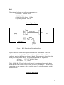
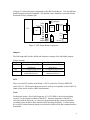
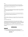
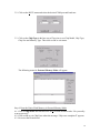
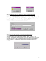
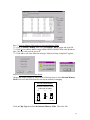
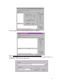
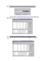
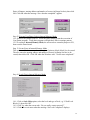
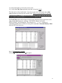
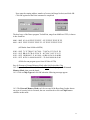
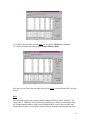
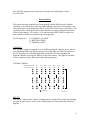
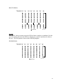
User’s Manual
Boot Strap Loader
Demo Kit
© 2000 Silicon Storage Technology, Inc. 414-01 6/00
The SST logo and SuperFlash are registered trademarks of Silicon Storage Technology, Inc. FlashFlex, In-Application
Programming, IAP and SoftLock are trademarks of Silicon Storage Technology, Inc. These specifications are subject to
change without notice.
1
User Manual for the FlashFlex51 Boot-Strap Loader Demo Kit (P/N: SST89CK77BSL)
Introduction ……………………………………………………………………………. 3
Getting Started …………………………………………………………………………
Unpacking the Demo Kit ………………………………………………………
System Requirements …………………………………………………………..
Windows 95/98 …………………………………………………………
DOS ……………………………………………………………………
3
3
4
4
5
Connecting the System ………………………………………………………………...
5
Hardware Description ………………………………………………………………….
Jumpers ………………………………………………………………………...
MCU …………………………………………………………………………...
Clock …………………………………………………………………………..
Power ………………………………………………………………………….
Reset …………………………………………………………………………..
RS-232 ………………………………………………………………………...
LEDs …………………………………………………………………………..
External Flash Memory Chip ………………………………………………….
5
6
6
6
7
7
7
7
7
Installing the Software ………………………………………………………………… 7
Windows 95/98 ………………………………………………………………... 7
DOS …………………………………………………………………………… 8
How to Use the Software ……………………………………………………………… 8
Windows 95/98 ………………………………………………………………... 8
DOS …………………………………………………………………………… 18
Demo Software ………………………………………………………………………..
Twoball ………………………………………………………………………..
Binctr .………………………………………………………………………..
Pendb .………………………………………………………………………..
21
21
21
22
Step-By-Step Procedure for Quick Demo …………………………………………….
Set up Demo System …………………………………………………………..
Erase All MCU Flash Memory ………………………………………………..
Download the BSL Code into Block 1 Flash Memory ………………………..
Activate Memory Re-mapping in External Memory Mode …………………..
Switch to Internal Memory Mode …………………………………………….
Download a Demo Program in Internal Memory Mode ……………………...
Execute Demo Program on Demo Board ……………………………………..
23
23
23
24
24
24
24
24
2
Introduction
The User Manual for the FlashFlex51 Boot-Strap Loader (BSL) Demo Kit provides the
user with the detailed information to quickly learn and use the kit. The manual, written
for the user of Windows 95/98 and DOS, walks the user through getting started, system
connections, hardware description, installing the software, how to use the software, a
description of the demo software, and a step-by-step procedure for a quick demo.
For future upgrades to this document, visit the MCU page on the SST Website, which is
www.SuperFlash.com.
Getting Started
Unpacking the Demo Kit
The demo kit consists of the following items:
1. Hardware
• BSL Demo Board
• 6-ft. DB-9 RS-232 Cable
• AC Adapter
2. Floppy Disk – v2.0A(Windows 95/98), with the following contents:
• Three demo programs (.a51 and .hex) - reside in folder “DemoProgram”:
- binctr.a51/.hex
- twoball.a51/.hex
- pendb.a51/.hex
The demo programs (.hex) are to be downloaded from the PC.
• External Memory Mode BSL program – resides in folder “ExtMemMode”:
- f51eble2.a51/.inc/.hex
- reg52a.inc
The hexadecimal code (.hex) needs a programmer to reprogram it into the
external flash memory chip U3 (SST39SF010 MPF) located on the demo
board.
• Internal Memory Mode BSL program – resides in folder “IntMemMode”:
- f51mble2.a51/.inc/.bin/.hex
- reg52a.inc
If the binary code (.bin) is downloaded, it is sent to block 1 flash memory,
or if the hexadecimal code (.hex) is downloaded, it is sent to block 0 flash
memory. The program code is configured for 11.0592 MHz, 38.4 KBaud
operation with an 89C58 device.
• Windows 95/98 executable code and MFC library files – reside in root
directory:
3
- FlashFlex51.exe
- Mfc42.dll and msvcrt.dll
The PC executable code (.exe) is designed for Windows 95/98. Two MFC
library files (.dll) are associated with PC executable code.
3. Floppy Disk – v1.1D (DOS), with the following contents:
• Three demo programs (.a51 and .hex) - reside in folder “bsl_demo”:
The description of these programs is the same as for item 2 above.
•
External Memory Mode BSL program – resides in folder “bslmpf11”:
- f51eble2.a51/.inc/.hex
- reg52a.inc
The hexadecimal code (.hex) needs a programmer to reprogram it into the
external flash memory chip U3 (SST39SF010 MPF) on the demo board.
• Internal Memory Mode BSL program – resides in folder “bslmcu11”:
- f51mble2.a51/.inc/.bin/.hex
- reg52a.inc
- f51pblb3.exe
- Readme.pdf
If the binary code (.bin) is downloaded, it is sent to block 1 flash memory,
or if the hexadecimal code (.hex) is downloaded, it is sent to block 0 flash
memory. The program code is configured for 11.0592 MHz, 38.4 KBaud
operation with an 89C58 device.
The PC executable code (.exe) is a menu-driven PC (DOS) interface code
communicating with the MCU BSL firmware.
The document file (.pdf) is the corresponding Readme file for the users of
BSL v1.1D.
•
Documentation
- Bsl_kit_UserManual.pdf
- Bsl_schematic.pdf
- Readme-v20A.pdf
The bsl_schematic.pdf provides the circuit diagram of the BSL Demo
Board. The Readme-v20A.pdf is the corresponding Readme file for the
users of BSL v2.0A.
System Requirements
Windows 95/98
The minimum hardware and software requirements are:
• Processor: Pentium or above
• RAM: 32 MByte
• Hard Disk Free Space: 2 MByte
• Operating System: Windows 95/98
4
DOS
The minimum hardware and software requirements are:
• Processor: 80486 or above
• RAM: 1 MByte
• Hard Disk Free Space: 1 MByte
• Operating System: DOS 6.2
Connecting the System
RS
232
RS-232 Cable
COM1-4
Demo
Board
PC
Power
Conn.
SST BSL 1.0
AC
Adapter
414 ILL F01.1
Figure 1. BSL Demo Board External Interfaces
Figure 1 shows the connections required to run the BSL Demo Board. The kit AC
Adapter, with a standard 0.2178 in.(5.5 mm) OD and 0.098 in.(2.5 mm) ID barrel
connector, provides the DC power to run the board. The connector is inserted into the
board power connector as shown. The specifications for the AC adapter are:
AC Input:
120 VAC, 60 Hz, 6 Watts
DC Output:
9 V, 300 mA
The 6 ft. DB-9 RS-232 serial cable (male/female) is next installed between the demo
board and the COM1/COM2/COM3/COM4 port of the interfacing PC. The hardware
connections are now complete, and the system is ready for software operation, which is
discussed below.
Hardware Description
5
In Figure 2 is shown the major components of the BSL Demo Board. Now the different
board functions are briefly explained. The detailed circuit schematic is presented in the
document file Bsl_schematic.pdf.
JP2 JP3 JP1
3
2
1
Y1
U1
Jumpers
LEDs U2
D8
U6 RS-232
Conn.
U3
U4
Power
Conn.
U5
U7
D1
LED
S1
RESET
D11
SST BSL 1.0
414 ILL F02.0
Figure 2. BSL Demo Board Components
Jumpers
The following table lists the default and alternative settings of the individual jumpers:
Jumper Settings:
Jumper
Default Setting
JP1
(closed) Start BSL Code
after Reset
JP2
(2+3) Internal Flash Active
JP3
(closed) LEDs D1-D8 are
connected to Port 1
Alternate Setting
(open) Start User Code
after Reset
(1+2) External Flash Active
(open) LEDs D1-D8 are not
connected to Port 1
MCU
There are two MCU sockets on the board: a PLCC socket (for U4) and a PDIP ZIF
socket (for U1). The board connections between sockets are in parallel, so that a MCU in
either socket can be used for a BSL demonstration.
Clock
On the demo board, a fixed clock frequency of 11.0592 MHz is derived by attaching
crystal Y1 to the internal oscillator of the MCU. Internal components of the MCU,
associated with the baud rate, are selectively programmed during system initialization
according to precalculated values dictated by the operating frequency. For that reason,
the crystal is soldered onto the board to insure that a reliable serial data communication is
maintained.
6
Power
+5V board power is derived from an on-board regulator circuit, centered upon the
LM7805C or equivalent voltage regulator chip (U7). The kit AC adapter transforms its
120VAC input into a +9V DC output, which is fed into the Power Connector on the
board and provides the input to the regulator circuit.
Reset
A hardware reset is accomplished using a dedicated reset chip (U5), either a DS1706L or
a MAX813LCP. When the Reset button (S1) is pressed, the RST output signal from U6
goes to a logic High to reset the MCU.
RS-232
Serial communication between the PC and the Receive (P3.0 RxD) and Transmit (P3.1
TxD) pins of the MCU utilizes an RS-232 Interface chip (the MAX232ACP chip in U6)
to perform the signal level shifting required for RS-232.
LEDs
Jumper JP3 enables or disables power to the eight (8) LEDs, which are tied to the Port 1
pins. The LEDs can be operated singly or together to provide user visibility of software
operation.
External Flash Memory Chip
The program in the External Flash Memory Chip (U3) allows the IAP commands
executing from the external memory device to program block 0 and 1 of the MCU (U1 or
U4) internal flash memory. This function allows the PC executable code to download the
BSL code into block 1 of the MCU internal flash memory. Jumper settings for the IAP
commands operation are: JP2 = (1+2) and JP1 can be either open or closed.
Note: If a SST89C54/58 MCU chip is in Level 4 Security Lock, then IAP operation
is inhibited.
Installing the Software
Windows 95/98
To install the executable software on the PC, insert the kit’s floppy disk (labeled as
v2.0A) into the floppy drive of the PC. Next perform the following steps:
1) Create a new folder, e.g. SSTBSL_V20A, and copy the following file(s) into it:
SSTFlashFlex51.EXE
MFC42.DLL*
MSVCRT.DLL*
7
*Copy this file when Windows’ Operating System error message asks for
it. See Step 3-1 in next section for a description of the error message.
2) Copy the following folders from v2.0A floppy disk into the new folder:
ExtMemMode
IntMemMode
DemoProgram
DOS
To install the executable software on the PC, insert the kit’s floppy disk (labeled as
v1.1D) into the floppy drive of the PC. Next perform the following steps:
1) Close all Window programs and exit to DOS.
2) From the DOS prompt, create a sub-directory by typing:
“C:\>MD C58-11MH”.
3) From the DOS prompt, change to the newly created sub-directory and copy the
PC executable and demo programs from the floppy disk. Type:
C:\>CD \C58-11MH <enter>
C:\ C58-11MH >COPY A:\BSLMCU11\F51PBLB3.EXE <enter>
C:\ C58-11MH >COPY A:\BSLMCU11\F51MBLE2.HEX <enter>
C:\ C58-11MH >COPY A:\BSL_DEMO\BINCTR.HEX <enter>
C:\ C58-11MH >COPY A: \BSL_DEMO\TWOBALL.HEX <enter>
C:\ C58-11MH >COPY A: \BSL_DEMO\PENDB.HEX <enter>
Once the PC executable is established, the user is ready to execute IAP commands from
either External or Internal Memory Mode and download one of the demo routines.
How to Use the Software
Windows 95/98
The MCU is an SST89C54/58 Rev.C1 or later and "unlocked". The following sixteen
steps walk the user through setting the external/internal memory mode, downloading the
BSL code or demo routines into internal flash memory, executing the memory-remap
command, uploading the code from internal flash memory and saving them as a disk file,
and locking the MCU chip.
Step 1. Prepare the Demo Kit for Running SST BSL v2.0A Program
1-1. Make the following jumper settings for External Memory Mode operation:
SST BSL DEMO BOARD
JUMPER SETTING FOR
EXTERNAL MEMORY MODE
(EXECUTE IAP CMD)
JP2
JP3
JP1
3
2
1
2-3: EA#=1
1-2: EA#=0
ON: LED
ON: BSL
OFF: USER
(DON’T CARE)
8
1-2. Check that the SST89C58 (PDIP) chip is inserted correctly in the ZIF socket (U1) –
the notch of chip lines up with the latch handle of socket.
1-3. Insure the SST39SF010 MPF (PLCC) chip is firmly inserted into the PLCC socket
(U3).
1-4. Connect the serial cable between the Demo board and the COM port of user PC.
1-5. Connect the barrel connector to the board and plug the AC adapter into an AC power
source. The yellow LED (D1, attached to port pin P1.0) and the red power indicator
should be ON.
Step 2. Load Program Files from Floppy Disk into User PC
Refer to the above section of “Installing the Software”.
Step 3. Start to Run the BSL v2.0A Program
3-1. Click on the executable file SSTFlashFlex51.EXE to run the BSL v2.0A program
and display the Entry Menu. If Window’s Operating System displays the following
error message, the user needs to copy two Microsoft Library files MFC42.DLL and
MSVCRT.DLL, from the Windows floppy disk into the same folder as the
executable file and restart the BSL executable program.
The following Entry Menu will appear:
9
3-2. Click on the RS232 menu and select the desired COM port and baud rate:
3-3. Click on the Chip Type in the box area of Functions to set Chip Model, Chip Type,
Chip Size and Memory Type. Then click on OK to exit menu.
The following menu for External Memory Mode will appear:
Step 4. Erase the Entire Flash Memory in External Memory Mode
4-1. Click on Chip Erase function and click on Yes when Windows asks: “Do you really
want to proceed?”
4-2. Click on OK to exit Chip Erase when the message “Chip erase completed!” appears.
4-3. Next reset the Demo board.
10
Step 5. Download the BSL Code into Block 1 Flash in External Memory Mode
5-1. Click on Download, then select the appropriate File Name and Starting Sector. The
BSL binary code, F51MBLE2.BIN which is stored in the folder of IntMemMode, needs
to be downloaded into block 1 at address F000h. The user needs to scroll down the list
box of Starting Addresses and click on “Sector 000 Addr=F000”.
5-2. Click on OK to exit menu and execute the download.
Step 6. Read BSL Code from Block 1 Flash in External Memory Mode
Click on Read, select the Start Address and Range, then click on OK.
The status of a sector could be one of three conditions – Blank, Not Blank or Not
Available. The content of a Blank sector shows all FFs. The content of a Not Blank sector
shows the hex format of data; all non-program spaces in user code are filled with 00s.
Hence, the content of an unread sector showing all 00s represents the status of Not
Available.
11
Step 7. Activate Memory Remapping in External Memory Mode
7-1. Click on Memory Remap, then select the Remap 1 Kbyte option and click OK.
7-2. Click Yes to redirect address range 0000h-03FFh to F000h-F3FFh when Windows
asks: “Do you really want to proceed?”
7-3. Click OK to exit menu when the message “Memory Remap Completed” appears.
Step 8. Switch to Internal Memory Mode
Change the jumper settings as shown in the following figure to enter Internal Memory
Mode. Next reset the Demo board to activate the memory-remapping.
SST BSL DEMO BOARD
JUMPER SETTING FOR
INTERNAL MEMORY MODE
(EXECUTE IAP CMD)
JP2
JP3
JP1
3
2
1
2-3: EA#=1
1-2: EA#=0
ON: LED
ON: BSL
OFF: USER
Click on Chip Type and select the Internal Memory Mode. Then click OK.
12
The following menu for Internal Memory Mode will appear:
Step 9. Download Demo/User Program in Internal Memory Mode
Click on Download, enter the Start Address (Sector 000 Addr=0000) and File Name, e.g.
Twoball.hex. Click OK to download code.
13
Step 10. Read Demo/User Code from Block 0 Flash in Internal Memory Mode
Click on Read, select the Start Address and Range (no. of sectors). Then click OK.
The Demo program Twoball.bin occupies three sectors, sector 000 through sector
002. User can click on sector number and the content of selected sector is shown in lower
half of window.
Step 11. Save Data into a File (Upload) from Block 0 in Internal Memory Mode
To save data into a binary/text file, the user needs to click on File menu then the Save
option.
14
Enter a filename, starting address and number of sectors (in Range list box), then click
OK. Click OK when the message “Save data has completed” appears.
Step 12. Execute User/Demo Code in Internal Memory Mode
12-1. Remove the jumper from JP1. Reset the Demo board to start the execution of
User/Demo program. Each demo program will light the LEDs in a unique pattern.
12-2.To return to Internal Memory Mode, the user needs to return the jumper to JP1,
then reset the Demo board.
Step 13. Sector Erase in Internal Memory Mode
This option enables the user to select the region of primary block (block 0) to be erased.
The user enters the starting address and number of sectors (in Range list box) to be
erased, then clicks OK. Click OK when the Windows asks: ”Sector erase completed!”
Step 14. Lock Chip in Internal Memory Mode
14-1. Click on Lock Chip option, select the level and type of lock, e.g. L3 Soft Lock
Block 0,1, then click OK.
14-2. Click Yes when the screen asks: “Do you really want to proceed?”
14-3. Click OK to exit menu when the message “Set Lock Completed” displays.
15
14-4. Reset the board to activate the security lock.
14-5. Select the Chip Type again (the procedure is listed in Step 8).
The chip can be soft or hard locked. Once the security lock is activated, only a chiperase operation can deactivate the security lock. Please be aware that the #5 selection
“L4 Hard Lock Block 0, 1” will activate the level-4 hard-lock, and only the chip-erase
command issued in SST89C5x External Host Mode can unlock it.
The Lock Chip option will no longer be shown once the Boot-Strap Loader detects the
chip is Soft Locked; instead, a message: “SECURITY: Block 0 & 1 ARE
SOFTLOCKED” will be displayed. The selection of ‘1’, ‘2’, or ‘5’ Hard Lock
commands prohibits the user from accessing IAP commands in Internal Memory Mode
after the MCU has been reset.
Step 15. Print Memory Contents
Click on File menu, then click on Print option.
16
Next enter the starting address, number of sectors (in Range list box) and click OK.
Click OK again after the Print command is completed.
The hard copy of the Demo program Twoball.bin, range from 0000h to 017Fh, is shown
in hex format as:
0000 – 000F 02 01 00 FF FF FF FF FF – FF FF FF FF FF FF FF FF
0010 – 001F FF FF FF FF FF FF FF FF – FF FF FF FF FF FF FF FF
(All blanks from 0010h to 00FFh)
0100 – 010F
0110 – 011F
0120 – 012F
0130 – 013F
74 3F 7B 06 F5 90 78 00 – 79 00 7A 02 31 26 03 1B
BB 00 F1 7B 06 F5 90 78 – 00 79 00 7A 02 31 26 23
1B BB 00 F1 21 00 18 00 – 00 B8 00 FA 19 00 00 B9
00 F4 1A 00 00 BA 00 EE – 22 00 00 00 00 00 00 00
All 00s for non-program space from 0139h to 017Fh)
Step 16. Return to External Memory Mode after Soft-Locked the Chip
16-1. Prepare the Demo Kit as delineated in Step 1. Set the jumpers for External
Memory Mode, then reset the board.
16-2. Click on Chip Type and click OK when the following message appear:
16-3. The External Memory Mode can’t be executed if the Boot-Strap Loader detects
any type of security lock is activated; the user would need to click on Chip Erase to
continue in this mode.
17
16-4. Follow the procedure listed in Step 4 to execute the Chip Erase command.
16-5. Reset the board and bring up the External Memory Mode.
Now the user can follow the procedure provided in Step 5 to download the BSL code into
block 1.
DOS
The following fourteen steps along with the Readme.pdf file (in folder “bslmcu11” on
floppy disk v1.1D(DOS)) can be used as the guidelines to walk the user through setting
the external/internal memory mode, downloading the BSL code or demo routines into
internal flash memory, executing the memory-remap command, uploading the data from
18
internal flash memory and saving them as a disk file, and locking the MCU chip. There
are 11 figures in the Readme.pdf file and these figures are referenced in the following
steps.
Step 1. Prepare the Demo Kit for Running SST BSL v1.1D Program
1.1. Follow the procedure listed in Step 1 in the Windows section.
Step 2. Start to run the BSL v1.1D Program
2-1. Close all Windows programs and exit to DOS.
2-2. From the DOS prompt, change to the newly created sub-directory by typing:
“C:\> cd \c58-11mh <enter>”
2-3. Run the PC executable program by typing:
“C:\C58-11MH>f51pblb3 <enter>”
Step 3. Select the External Memory Mode from Entry Menu
3-1. Enter ‘2’ to select “External Memory Mode” on the Entry Menu.
Refer to “Figure 2. Menu Driven User Interface of the Boot-Strap Loader(v1.1D)”
in Readme.pdf.
3-2. Enter ‘58’, ‘1’ and ‘1’ to select Chip Number, COM Port and Baud Rate.
Refer to “Figure 8. Step-by-Step Example of Selecting Chip Number 89C58 and
COM Port 1 in External Memory Mode of Boot-Strap Loader(v1.1D for
39SF010)”.
Step 4. Erase the Entire Flash Memory in External Memory
4-1. On the External Memory Mode Sub-Menu, enter ‘4’ to execute chip-erase command.
Enter ‘y’ or ‘Y’ to proceed when the screen asks: “Proceed Chip_Erase command?
(Y/N)”.
4-2. Next reset the Demo board.
Step 5. Download the BSL Code into Block 1 Flash in External Memory Mode
5-1. Enter ‘2’ to download code into Block 0/1 Flash.
Refer to “Figure 11. Step-by-Step Example of Download BSL Code(v1.1D for
89C58 into Block 1 and Re-mapping 1 KB of Flash in Ext. Mem. Mode”.
Step 6. Upload BSL Code from Block 1 Flash in External Memory Mode
6-1. Enter ‘3’ to upload data from Block 0/1 Flash.
6-2. Enter ‘n‘ or ‘N’ to skip the creation of a text format file.
6-3. Enter “bsl_blk1.bin” when the screen asks: “Input full name of file: ”.
6-4. Enter “f000” when the screen asks: “Enter start address(in 40H/80H increments): ”.
6-5. Enter “400” when the screen asks: “Enter number of bytes to read in Hex: “. The
400H is an estimated value of the BSL code size.
Step 7. Activate Memory Remapping in External Memory Mode
7.1. Enter ‘5’ to execute memory_remap command.
Refer to the figure mentioned at Step 5-1.
19
Step 8. Switch to Internal Memory Mode
8-1. Make the jumper settings listed in “Step 8” of the Windows section.
8-2. Reset the Demo board to activate the memory-remapping.
8-3. Enter ‘0’ to return to Entry Menu
8-4. Enter ‘1’ to switch to Internal Memory Mode.
8-5. Follow “Step 3-2” for the selection of Chip Number, COM Port and Baud Rate.
Step 9. Download Demo/User Program in Internal Memory Mode
9.1. In the Readme file (DOS), follow the sequence listed in “Figure 9. Step-by-Step
Example of Downloading BSL Demo code into block 0 and Executing the Demo code in
Internal Memory Mode”.
Step 10. Upload Demo/User Code from Block 0 Flash in Internal Memory Mode
10.1. In the Readme file (DOS), follow the sequence listed in “Figure 10. Step-by-Step
Example of Uploading a BSL Demo code from block 0 into a disk file in Internal
Memory Mode”.
Step 11. Blank Check in Internal Memory Mode
11-1. Enter a valid starting address (in Hex), e.g. 1000, when the screen asks:
“Enter start address (should be in 80H increments): “.
11-2. Enter a valid number of sectors (in decimal), e.g. 40, when the screen asks:
“Enter the number of sectors (in decimal) to be checked: “.
11-3. The program displays the message “SPECIFIED SECTOR OR SECTORS
ARE ALL BLANK!” at the STATUS field if the region to be checked are all blanks.
Otherwise, the message “SPECIFIED SECTOR OR SECTORS ARE NOT BLANK!” is
displayed.
Step 12. Execute User/Demo Code in Internal Memory Mode
12.1. Follow the procedure listed in Step 12 in the Windows section.
Step 13. Sector Erase in Internal Memory Mode
13-1. Enter a valid starting address (in Hex), e.g. 1000, when the screen asks:
“Enter start address (should be in 80H increments): “.
13-2. Enter a valid number of sectors (in decimal), e.g. 40, when the screen asks:
“Enter the number of sectors (in decimal) to be erased: “.
13-3. The program displays the message “SUCCESS IN SECTOR ERASING!”
at the STATUS field after a success operation achieved. Otherwise, the message
“SECTOR ERASE FAILURE!” is displayed.
Step 14. Lock Chip in Internal Memory Mode
14-1. Enter ‘6’ to Lock Chip.
14-2. Referring to “Figure 6. Sub-Menu Flowchart of Security Lock for the BSL v1.1D”,
select the type of security lock, e.g. “3. L3 SoftLock block 0&1”.
14-3. Reset the Demo board.
14-4. Enter ‘0’ to return to Entry Menu, then enter ‘1’ to switch to Internal Mem. Mode.
14-5. Follow “Step 3-2” for the selection of Chip Number, COM Port and Baud Rate.
20
14-6. The BSL program detects the status of security lock and displays it in the
STATUS field.
Demo Software
Three demo software programs have been supplied with the BSL Demo Kit, and the
intent here is provide the user with some understanding of their basic functionality. Any
one of them can be downloaded from the PC to the Demo Board, and executed there. For
a visible presence on the demo board, each of the demo routines manipulates the board
LEDs in some manner. The source (.A51) and download (.HEX) files for each of the
three software routines are included on the kit floppy disk.
The file names are:
1) TWOBALL.A51/.HEX
2) BINCTR.A51/HEX
3) PENDB.A51/HEX
TWOBALL
The “twoball” routine corresponds to a two-ball bouncing ball sequence, that is, the two
most significant LEDs will light up and proceed to shift right one LED bit position at a
specific time interval. When the lighted pair reaches the two least significant bit
positions, then they will begin to shift left in the same manner. The right-left sequence
will be continuous, and is illustrated in the following diagram:
TWOBALL DEMO:
PORT 1 BITs PL0
LED DISPLAYS D1
PL1
D2
PL2
D3
PL3
D4
LIGHT ON
PL4
D5
PL5
D6
PL6
D7
PL7
D8
414 ILL F03.0
BINCTR
The “binctr” routine shows a binary counting sequence on the LEDs, which are changing
at a specific time interval. Some of the counting states are illustrated in the following
diagram:
21
BINCTR DEMO:
PORT 1 BITs PL0
LED DISPLAYS D1
PL1
D2
PL2
D3
PL3
D4
PL4
D5
PL5
D6
PL6
D7
LIGHT ON
PL7
D8
414 ILL F04.0
PENDB
The “pendb” software routine causes the LEDs to behave similar to a pendulum. Like the
previous routines discussed, the LEDs are changing at a specific time interval visible to
the user. The LED pattern is shown in the following diagram:
PENDB DEMO:
PORT 1 BITs PL0
LED DISPLAYS D1
PL1
D2
PL2
D3
PL3
D4
PL4
D5
LIGHT ON
PL5
D6
PL6
D7
PL7
D8
414 ILL F05.0
22
Step-By-Step Procedure for Quick Demo
The purpose of this procedure is to provide the user with the sequence of steps to quickly
demonstrate the Boot-Strap Loader(BSL) Demo Kit software under Windows 95/98. It
assumes that the user has previously become familiar with the kit, and needs this step-bystep procedure as a refresher. It further assumes that the BSL Demo Kit software has
already been installed on the user’s PC and that the MCU does not contain any BSL code.
The procedure will sequence through the following functions:
set up demo system, erase the chip, download the BSL code and activate memory
re-mapping in External Memory Mode;
download one of the three demo programs in Internal Memory Mode, and
finally, execute the downloaded demo program on the Demo board.
Set up Demo System
1. Set up the BSL Demo board for External Memory Mode operation.
a. Realize the following jumper settings on the Demo board:
JP1: Closed
JP2: 1 + 2
JP3: Closed
b. Connect the RS-232 DB-9 cable between the Demo board and PC.
c. Connect the AC adapter to the Demo board.
2. Start the PC software.
a. Run the BSL v2.0A executable program: FlashFlex51.exe
b. The Entry Menu will appear.
3. Select COM port, baud rate, chip type and memory mode.
a. On the Entry Menu, click on the RS-232 option then select the desired COM port
and baud rate. COM1 and 38.4Kbits/second are the default values. Click OK to
exit menu.
b. Next click on the Chip Type in the Functions area of the Entry Menu. From its
menu, select the chip model (SST89), type (C) and size (58) as well as the
memory type (External Memory). Click OK to exit menu.
c. The External Memory Mode menu now appears, which means that the system is
setup and ready to execute any of the External Memory Mode command
functions.
Erase All MCU Flash Memory
1. Under Functions on the External Memory Mode menu, click on Chip Erase and click
on Yes when Windows asks: “Do you want to proceed?”
2. Click on OK to exit Chip Erase when the message “Chip erase completed!” appears.
3. Next reset the Demo board.
23
Download the BSL Code into Block 1 Flash Memory
1. Under Functions on the External Memory Mode menu, click on Download , then
select the appropriate File Name and Starting Sector. The BSL code file name is
f51mble2.bin, which is in the IntMemMode folder. For Starting Address, click on
“Sector 000 ADDR=F000”. Click on OK to exit menu and execute the download.
2. The BSL code now resides in Block 1 Flash memory.
Activate Memory Re-mapping in External Memory Mode
1. Click on Memory Remap, then select the Remap 1Kbyte option and click OK.
2. Click Yes to redirect address range 0000h-03FFh to F000h-F3FFh when Windows
asks: “Do you really want to proceed?”
3. Click OK to exit menu when the message “Memory Remap Completed” appears.
Switch to Internal Memory Mode
1. Change the Demo board jumper JP2 setting to the following:
JP2: 2 + 3
2. Next reset the Demo board to activate the memory re-mapping.
3. Click on Chip Type and select the Internal Memory Mode. Then click OK.
4. The Internal Memory Mode menu now appears.
Download a Demo Program in Internal Memory Mode
1. On the Internal Memory Mode menu, click on Download.
2. Enter the File Name. From the DemoProgram folder, choose one of the three demo
programs listed there: twoball.hex, binctr.hex or pendb.hex.
3. From the Starting Sector options, select Sector 000 Addr=0000. Click on OK to
execute the download.
Execute Demo Program on Demo Board
1. Remove the JP1 jumper (JP1: Open) to run user code.
2. Reset the Demo board to cause the MCU to begin executing the downloaded demo
program.
3. Now the LED bank will be showing the unique lighting activity associated with the
selected demo program.
24