1
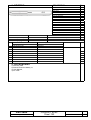
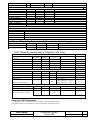
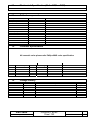
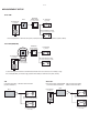
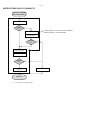
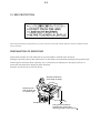
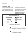
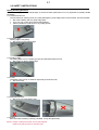
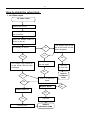
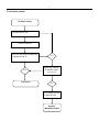
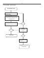
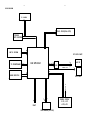
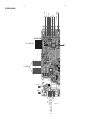
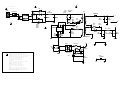
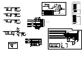
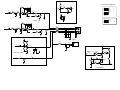
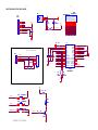
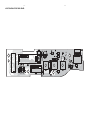
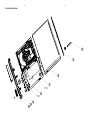
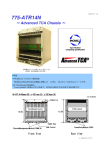
DVP360 DVD player CONTENTS Pr oReader Dr ive Technical specification .....................................................................1 Service and safety instructions.........................................................2 How to remove the CD manually from the tray...............................2-1 How to check the return Unit...................................................2-2..2-5 Software Upgrades and How to select right language............2-6..2-7 Wiring diagram...............................................................................3-1 Block diagram.................................................................................3-2 Main board Circuit diagram...................................................................4-1..4-6 Layout diagram..........................................................................4-7 Front panel board Circuit diagram..........................................................................5-1 Layout diagram..........................................................................5-2 Exploded view diagram..................................................................6-1 Revision list....................................................................................7-1 © Copyright 2011 Philips Consumer Electronics B.V. Eindhoven, The Netherlands All rights reserved. No part of this publication may be reproduced, stored in a retrieval system or transmitted, in any form or by any means, electronic, mechanical, photocopying, or otherwise without the prior permission of Philips. Published by SW 1138 Service Audio Version 1.0 Subject to modification 3141 785 3680 DESCRIPTION 1. EPICTION Pos DVD door Open /Close button Play/Pause Power button Power and play indicator Remote IR Sensor CABINET Dimensions (L x W x H): TBA Bear unit weight (kg) Main set CVBS &YUV OUTPUT X 1 L/R OUTPUT X 1 COAXIAL OUTPUT X 1 HDMI OUTPU X 1 TBA Connector type RCA4 x1 RCA 2x1 RCA x1 HDMI x1 Material: Refer to Cosmetic Specification Finishing: Refer to MUS specification 2. ACCESSORIES 1) Warranty Card 2) Remote Control w/battery x1, 3) User Manual, 4) AV cable DVP3680 Page 3 of 8 PRODUCT SPEC Sheet-190 Rev.1.0 3. General Description DVD player Key Components: Optical Pickup: S76RFXP2 (IM) Chip set/Solution: MT1389DXE-G Disc Size: 8cm/12cm Playable disc type: DVD/DVD+RW/DVD+R/CD/CD-R/CD-RW / DVD-R/-RW Video output signal: PAL/AUTO/NTSC (output only, with Macrovision) Video format: DVD / VCD / SVCD / JPEG / Audio format: CD/MP3, MP3-DVD, Dobly digital (down mix), WMA User Interface: OSD language: Russian/English/ Ukrainian for 51 version English,Trad-Chinese, Beharsa Melayu. Thai, Korean for 98 version Eng, Simplified-Chinese for 93version Eng, Trad-Chinese, Malay, for 96 version (Detail, refer to UI requirement) Screen Saver function. Button functions: Refer to MUS. Standby power: <0.5W Picture Quality: Sound Quality: refer to DVP3500K/98 (NO VIDEO BUFFER) refer to DVP3500K/98 (NO OUTSIDE 2CH AUDIO DA) Lifetime : 3 years (min.) Temperature & Humidity: Operating Temperature & Humidity 0-50 deg C / 30-90%; Charging Temperature: 0 - +40 degC Storage Temperature & Humidity -20-70 deg C / 30-95% Climatic requirements, Indoor product Weight: TBC Kg +/- 30% with / battery / AV cable / IFU / GB Version Region Countries 51 93 96 98 5 6 3 3 Russia / Ukraine China Taiwan Asia DVP3680 Page 4 of 8 Voltage Frequency AC Cord Type 230V 110V‐ 240V 110V‐ 240V 110V‐ 240V 50Hz 50Hz,60Hz 50Hz,60Hz 50Hz,60Hz PRODUCT SPEC Sheet-190 VDE 2‐pins round CCC flat 2‐pin Taiwan Plug (CNS 690 approved) VDE 2‐pins round Rev.1.0 4. Safety requirements CB approval DVP3600 IEC60065:2001 + A1:2005 & EN60065:2002 + A1:2006, (LVD directive 2006/95/EC) 5. EMC requirements – Active Radiation, Radiation Immunity, Conductive Interference DVP3600 EN55013: 2001 +A1:2003 + A2:2006 EN55020: 2007 EN61000-3-2: 2006 EN61000-3-3: 1995 + A1: 2001 + A2:2005 (EMC directive 2004/108/EC) 6. EUP test IEC62301: 2005 1st edition (commission regulation (EC ) No 1275/2008) (EUP directive 2005/32/EC) 7. Power-Supply AC Power Power Supply voltage Supply Power consumption Standby Power (power switch OFF) Typical 100- 240V 10W - Limit +/- 10% +40%/ - 0% <0.5W Remarks 8. Audio (all test with 22k Ohm load unless specified) DVD-Audio Line out 1. Output voltage 1kHz (V) 2. THD Condition 20-20kHz 3. Dynamic range 4. A-weighted S/N ratio 5. Frequency response 6. Channel separation 7. Channel balance Typical Limit 2Vrms +/- 1dB 0.03% 0.06% 1kHz Tr15/Tr49 20-20kHz 1kHz 1kHz - Apply 8 ohm loading no component damage >85dB >90dB +1 / -0.5dB >=85dB +/- 1dB Digital output Coaxial Type CDDA/LPCM (including MPEG1) MPEG2, Dolby Digital (AC-3) DTS, 96kHz 24 bit Standard IEC60958 IEC61937 9. Video Output AV output ports special requirement Connection Port Impedance >10V DC 75 ohm No component damaged CVBS Video Output (PAL / NTSC) DVD-Video composite 1. White Bar DVP3680 Page 5 of 8 Condition Typical Limit - 714mVpp +10/-20 PRODUCT SPEC Sheet-190 Rev.1.0 2. Sync. Amplitude 3. Amplitude o/p 4. Burst amplitude 5. Burst/chroma ratio 6. S/N luminance 7. S/N chroma (AM) 8. S/N chroma (PM) 9. Video bandwidth 10 Chroma/Luminance 11 Sub-carrier frequency (Chroma) (ppm) Un-weighted Un-weighted Un-weighted - 286mVpp 1000mVpp 286mVpp PAL/8MHz - 4.43361875MHz / PAL 3.579545MHz / NTSC 12 Subcarrier locked / unlocked - - 10. +/-40 +10/-20 +1/-4 +/-10 >55 >55 >52 -7 <100 +/-30 Locked YUV Video Output Description Test Signal Specification NTSC PAL 714 mVpp 700 mVpp +/+/- 10% 10% 300 mVpp 286 mVpp +30mV / +/- 40mV 50mV 286mV ± 300mV ± 40mV 50mV 525mV ± 525mV ± 10% 10% 100% White Y White level 100% White Sync.amplitude 75% color bar T2 C1 ) 75% Colour bar U amplitude o/p V amplitude o/p S/N on outputs: U V Video Bandwidth (0.5MHz10MHz) ( 100% red ( T2 C17 ) Multi-burst 55 dB* 55 dB +1dB/-6dB +1dB/-6dB Class achievement NTSC PAL video amplitude Ref. 0dB 90.8 IRE +1dB / 1dB +1dB / 1dB +1dB / 2dB +1dB / 3dB +1dB / 5dB +1dB / 10dB 0.5MHz multi-burst 1.0MHz ( T2 C9 ) 2.0MHz 4.0MHz 4.8MHz 5.8MHz +1dB / -1dB +1dB / -1dB +1dB / -2dB +1dB / -3dB +1dB / -5dB +1dB / -10dB View test: For both NTSC and PAL a viewing test is necessary to determine any annoying phenomena which can not be determined by standard video measuring procedures. In case of the doubt, the viewing test is decisive 11. Miscellaneous Electrical 1. EMC for EURO 2. ESD test(UAN-D1724) 3. Mains spike 4. Mains failure 5. Laser beam shut off when the CD door open Auto Power Off - 4dB Ok Ok Ok Ok - - Ok Con DVP3680 Page 6 of 8 EMC <= 8kV <= 15KV +/-1500V 100% mains drop Typical Below Limit No abnormal allowed No component damage Refer to CTQ Limit PRODUCT SPEC Sheet-190 Rev.1.0 Screen saver Power off –stand by IR remote Max. operating (degree) Quiescent Current Operating Voltage Operating Current Carrier Frequency Battery Storage Time Battery Life Time - 20 20 Condition <= +/- 45。 <= +/- 30。 0。 +/-30% +/-30%- Typical 2.3 - 3.5V 9 – 16mA 36KHz ? Year After push / disc stop After Screen saver functional Limit 5 7 10 <1uA (M) (M) (M) +/- 2% Temperature: After 20 hours continuous sending (2s/time), IR power should be at least 20μW/cm2 Audio/ Video Characteristic Testing discs Manufacturer Disc name 1) TOSHIBA TSD-4 2) DOLBY Test disc 3) ABEX TDV-540A 4) SONY Test CD Type 4 12. Playability Requirement (See attached in last page). DISC Playability (details refer to Playability Test Plan) DVD Video playability 1. Scratch 2. Black dot 3. Fingerprint 4. Non-Centre 5. Vertical deviation disc DVD+ RW Video playability Condition Typical Limit - - <=1.6 NA NA NA NA Condition Typical Normal playback Black dot Fingerprint Philips marginal DVD-9 CD playability Condition Abex-TCD732RA(VDD) Track 15 Abex-TCD713(ECC 210um) Typical ABEX TDV-541 ABEX TDV-545 ABEX TDV-545 ABEX TDV-552 ABEX TDV-562 Limit OK 0.8 OK Philips HAC11 Philips HAC11 Philips HAC11 OK Philips LVP12.01 – layer 0 Philips LVP12.02 – Layer 1 Limit OK NA Power On / Off Disturbances > -52 dB suppression of the disturbance with regard to the rated output voltage. The peak level has to be measured according to IEC 60651 weighted (A) curve. DVP3680 Page 7 of 8 PRODUCT SPEC Sheet-190 Rev.1.0 13. Mechanical Specification (Refer PQR or PQP) 14. Critical component Description DVD Chip set Laser pick up Remote Control Power IC LOADER Motor Driver IC Manufacturer MTK IM TianZeHuan Infineon KeQin SEMICO EON/MX MIRA/ETRON/ESMT FLASH(16M) SDRAM(4M X16BIT) 15. Model no. Version MT1389QE/DE/DXE-J S76RFXP2 T47 ICE3B0565J RT-628 CD588CB EN25QH16-104HIP/MX25L1606EM2I-12G EM638165TS-6G/M12L64164A-7TG/AT Cosmetic Specification All cosmetic color please refer Philips MUS color specification No. Part Description 16. Texture Finishing Color Remarks Change History Version 1.0 Date 2011-07-19 DVP3680 Page 8 of 8 Description by Wang S.F initial PRODUCT SPEC Sheet-190 Rev.1.0 2-1 MEASUREMENT SETUP Tuner FM DUT RF Generator Bandpass 250Hz-15kHz LF Voltmeter e.g. 7122 707 48001 e.g. PM2534 Ri=50: e.g. PM5326 S/N and distortion meter e.g. Sound Technology ST1700B Use a bandpass filter to eliminate hum (50Hz, 100Hz) and disturbance from the pilottone (19kHz, 38kHz). Tuner AM (MW,LW) DUT Bandpass 250Hz-15kHz LF Voltmeter e.g. 7122 707 48001 e.g. PM2534 RF Generator e.g. PM5326 S/N and distortion meter Ri=50: e.g. Sound Technology ST1700B Frame aerial e.g. 7122 707 89001 To avoid atmospheric interference all AM-measurements have to be carried out in a Faraday´s cage. Use a bandpass filter (or at least a high pass filter with 250Hz) to eliminate hum (50Hz, 100Hz). Recorder CD Use Audio Signal Disc (replaces test disc 3) SBC429 4822 397 30184 Use Universal Test Cassette CrO2 SBC419 4822 397 30069 or Universal Test Cassette Fe SBC420 4822 397 30071 LF Generator DUT e.g. PM5110 L DUT L R R S/N and distortion meter S/N and distortion mete e.g. Sound Technology ST170 e.g. Sound Technology ST1700B LEVEL METER e.g. Sennheiser UPM550 with FF-filter LEVEL METER e.g. Sennheiser UPM550 with FF-filter 2-2 INSTRUCTIONS ON CD PLAYABILITY Customer complaint "CD related problem" Set remains closed! check playability 1 playability ok ? N Y "fast" lens cleaning 3 For flap loaders (= access to CD drive possible) cleaning method 4 is recommended check playability playability ok ? N Y Play a CD for at least 10 minutes check playability playability ok ? N Y add Info for customer "SET OK" 2 return set 1 - 4 For description - see following pages Exchange CDM 2-3 INSTRUCTIONS ON CD PLAYABILITY 1 PLAYABILITY CHECK 4 LIQUID LENS CLEANING For sets which are compatible with CD-RW discs use CD-RW Printed Audio Disc ....................7104 099 96611 TR 3 (Fingerprint) TR 8 (600µ Black dot) maximum at 01:00 • playback of these two tracks without audible disturbance playing time for: Fingerprint 10seconds Black dot from 00:50 to 01:10 • jump forward/backward (search) within a reasonable time For all other sets use CD-DA SBC 444A..................................4822 397 30245 TR 14 (600µ Black dot) maximum at 01:15 TR 19 (Fingerprint) TR 10 (1000µ wedge) • playback of all these tracks without audible disturbance playing time for: 1000µ wedge 10seconds Fingerprint 10seconds Black dot from 01:05 to 01:25 • jump forward/backward (search) within a reasonable time 2 CUSTOMER INFORMATION It is proposed to add an addendum sheet to the set which informs the customer that the set has been checked carefully - but no fault was found. The problem was obviously caused by a scratched, dirty or copy-protected CD. In case problems remain, the customer is requested to contact the workshop directly. The lens cleaning (method 3) should be mentioned in the addendum sheet. The final wording in national language as well as the printing is under responsibility of the Regional Service Organizations. Before touching the lens it is advised to clean the surface of the lens by blowing clean air over it. This to avoid that little particles make scratches on the lens. Because the material of the lens is synthetic and coated with a special anti-reflectivity layer, cleaning must be done with a non-aggressive cleaning fluid. It is advised to use “Cleaning Solvent The actuator is a very precise mechanical component and may not be damaged in order to guarantee its full function. Clean the lens gently (don’t press too hard) with a soft and clean cotton bud moistened with the special lens cleaner. The direction of cleaning must be in the way as indicated in the picture below. 2-4 2.0 SAFTETY INSTRUCTIONS GB NL ESD WARNING Alle IC’s en vele andere halfgeleiders zijn gevoelig voor electrostatische ontladingen (ESD). Onzorgvuldig behandelen tijdens reparatie kan de levensduur drastisch doen verminderen. Zorg ervoor dat u tijdens reparatie via een polsband met weerstand verbonden bent met hetzelfde potentiaal als de massa van het apparaat. Houd componenten en hulpmiddelen ook op ditzelfde potentiaal. All ICs and many other semi-conductors are susceptible to electrostatic discharges (ESD). Careless handling during repair can reduce life drastically. When repairing, make sure that you are connected with the same potential as the mass of the set via a wrist wrap with resistance. Keep components and tools also at this potential. F ATTENTION Tous les IC et beaucoup d’autres semi-conducteurs sont sensibles aux décharges statiques (ESD). Leur longévité pourrait être considérablement écourtée par le fait qu’aucune précaution n’est prise à leur manipulation. Lors de réparations, s’assurer de bien être relié au même potentiel que la masse de l’appareil et enfiler le bracelet serti d’une résistance de sécurité. Veiller à ce que les composants ainsi que les outils que l’on utilise soient également à ce potentiel. WAARSCHUWING D I WARNUNG Alle ICs und viele andere Halbleiter sind empfindlich gegenüber elektrostatischen Entladungen (ESD). Unsorgfältige Behandlung im Reparaturfall kan die Lebensdauer drastisch reduzieren. Veranlassen Sie, dass Sie im Reparaturfall über ein Pulsarmband mit Widerstand verbunden sind mit dem gleichen Potential wie die Masse des Gerätes. Bauteile und Hilfsmittel auch auf dieses gleiche Potential halten. AVVERTIMENTO Tutti IC e parecchi semi-conduttori sono sensibili alle scariche statiche (ESD). La loro longevità potrebbe essere fortemente ridatta in caso di non osservazione della più grande cauzione alla loro manipolazione. Durante le riparazioni occorre quindi essere collegato allo stesso potenziale che quello della massa dell’apparecchio tramite un braccialetto a resistenza. Assicurarsi che i componenti e anche gli utensili con quali si lavora siano anche a questo potenziale. GB Safety regulations require that the set be restored to its original condition and that parts which are identical with those specified, be used. “Pour votre sécurité, ces documents doivent être utilisés par des spécialistes agréés, seuls habilités à réparer votre appareil en panne”. NL Veiligheidsbepalingen vereisen, dat het apparaat bij reparatie in zijn oorspronkelijke toestand wordt teruggebracht en dat onderdelen, identiek aan de gespecificeerde, worden toegepast. CLASS 1 LASER PRODUCT 3122 110 03420 F Les normes de sécurité exigent que l’appareil soit remis à l’état d’origine et que soient utiliséés les piéces de rechange identiques à celles spécifiées. GB Warning ! Invisible laser radiation when open. Avoid direct exposure to beam. D Bei jeder Reparatur sind die geltenden Sicherheitsvorschriften zu beachten. Der Original zustand des Geräts darf nicht verändert werden; für Reparaturen sind Original-Ersatzteile zu verwenden. I Le norme di sicurezza esigono che l’apparecchio venga rimesso nelle condizioni originali e che siano utilizzati i pezzi di ricambio identici a quelli specificati. "After servicing and before returning set to customer perform a leakage current measurement test from all exposed metal parts to earth ground to assure no shock hazard exist. The leakage current must not exceed 0.5mA." S Varning ! Osynlig laserstrålning när apparaten är öppnad och spärren är urkopplad. Betrakta ej strålen. SF Varoitus ! Avatussa laitteessa ja suojalukituksen ohitettaessa olet alttiina näkymättömälle laserisäteilylle. Älä katso säteeseen! DK Advarse ! Usynlig laserstråling ved åbning når sikkerhedsafbrydere er ude af funktion. Undgå udsaettelse for stråling. Caution: These servicing instructions are for use by qualified service personnel only. To reduce the risk of electric shock do not perform any servicing other than that contained in the operating instructions unless you are qualified to do so. 2-5 2.1 ESD PROTECTION Whenthepowersupplyisbeingturnedon,youmaynotremovethislasercautionslabel.Ifitremoves,radiationoflaser maybereceived. PREPARATIONOFSERVICING PickupHeadconsistsofalaserdiodethatisverysusceptibletoexternalstaticelectrocity. Althoughitoperatesproperlyafterreplacement,ifitwassubjecttoelectrostaticdischargeduringreplacement, itslifemightbeshortened.Whenreplacing,useaconductivemat,solderingironwithgroundwire,etc.to protectthelaserdiodeformdamagebystaticelectricity. Andalso,theLSIandICaresameasabove. Groundconductive wriststrapforbody. Solderingiron withgroundwire orceramictype 1M Conductivemat Thegroundresistance betweenthegroundline andthegroundislessthan10 2-6 SAFTY NOTICE SAFTY PRECAUTIONS LEAKAGE CURRENT CHECK Plug the AC line cord directly into a 120V AC outlet (do Measure the AC voltage across the 1500 not use an isolation transformer for this check). Use an AC voltmeter, having 5000 per volt or more sensitivity. The test must be conducted with the AC switch on and then repeated with the AC switch off. The AC voltage Connect a 1500 indicated by the meter may not exceed 0.3V.A reading 10W resistor,paralleled by a 0.15uF resistor. 150V AC capacitor between a knomn good earth ground (water pipe, conduit, etc.) and all exposed metal parts of exceeding 0.3V indicates that a dangerous potential exists, the fault must be located and corrected. cabinet (antennas, handle bracket, metal cabinet screwheads, metal overlays, control shafts, etc.). Repeat the above test with the DVD VIDEO PLAYER power plug reversed. NEVER RETURN A DVD VIDEO PLAYER TO THE CUSTOMER WITHOUT TAKING NECESSARY CORRECTIVE ACTION. READING SHOULD NOT EXCEED 0.3V AC VOLTMETER DVD VIDEO PLAYER (5000 per volt or more sensitivity) 1500 10W AC OUTLET Good earth ground such as a water pipe, conduit, etc. 0.15uF 150V AC Test all exposed metal. Voltmeter Hook-up for Leakage Current Check The lightning flash with arrowhead symbol, within an equilateral triangle, is intended to alert the user to the presence of uninsulated "dangerous voltage" within the product's enclosure that may be of sufficient magnitude to constitute a risk of electric shock to persons. The exclamation point within an equilateral triangle is intended to alert the user to the presence of important operating and maintenance (servicing) instructions in the literature accompanying the appliance. 2-7 2.2 SAFETY INSTRUCTIONS Battery Handling Guideline Since the battery is packed in soft package, to ensure its better performance, it’s very important to carefully handle the battery 2.2.1 Soft Aluminium foil The soft aluminum packing foil is very easily damaged by sharp edge parts such as Ni-tabs, pins and needles. • Don’t strike battery with any sharp edge parts • Trim your nail or wear glove before taking battery • Clean worktable to make sure no any sharp particle 2.2.2 Sealed edge Sealing edge is very flimsy • Don’t bend or fold sealing edge 2.2.3 Folding edge The folding edge is form in battery process and passed all hermetic test. • Don’t open or deform folding edge 2.2.4 Tabs The battery tabs are not so stubborn especially for aluminum tab. • Don’t bend tab 2.2.5 Mechanical shock • Don’t Fall, hit, bend battery body 2.2.6 Short Short terminals of battery is strictly prohibited, it may damage battery. Caution: Danger of explosion if battery is incorrectly replaced. Replace only with the same or equivalent type. 2-1 How to remove the CD manually from the tray 1. Please do as below instruction in case the tray can not be open: a. Power off the DVD player. b. Please gently push the guider and wait until the tray comes out(Figure1). use jig move this part left 2-2 How to check the return Unit 1, No Video output No Video output Connect the AV OK Insert the AC Power line into the connectors Press the standby button to power on the set The display on the set OK NG The “Philips” logo should be on the screen and the witch will display NG OK The “Philips” logo should be on the screen and the witch will display Insert the AC power line over again NG NG OK TEST 1.2V and 3.3V Power Replace Q5,Q6 Replace flash U11 NG NG The DSP Fail PSU Fail Replace Mainboard PCBA The LED module Fail Replace frontboard PCBA NG 2-3 2, No Audio output No Audio output Connect the AV OK Power on the set Play the disc and the audio will output from the TV NG OK Adjust the volume + to add the volume from the TV Test Finish NG The Audio DA Fail or the DSP Fail Replace Mainboard PCBA 2-4 3, No KARAOKE Audio output No KARAOKE output Check the Audio output when DVD/CD PLAY play the KARAOKE disc and then set the menu of setup and to set the kalaok to on Sing with MICROPHONE and the audio will output from the TV OK Test Finish NG check the MICROPHONE is on NG The Karaoke board is broken . Replace The Karaoke board PCBA 2-5 4, No playing any discs No playing any discs Connect the AV OK Power on the set Open the tray door and put into the DVD or CD disc to closing the tray door The servo chip or DSP chip fail The system will loading the disc, and on the screen display the ‘Loading’ OSD The disc’s info display the screen NG Replace Mainboard PCBA NG will Replace LOADER and check again NG The loader or servo chip or DSP chip fail Note to hear the playback sound when close the tray door to playing the disc NG NG Please power off, then power on the set to playback the disc over again 2-6 Software upgrade 1. Get the software firmware,the name must be DVP36XX_XX.BIN, and all character must be large. or press SETUP key on the RC,in “ Preferences” menu can see the option of “Version info”, Then, enter the Version info menu and you can see its upgrade file which shown of File Name 2. Copy the upgrade firmware onto CD disc. 3. Play the firmware CD disc,and the upgrade menu will appear. Upgrade file detected Upgrade ? press PLAY to start 4. First Select PLAY button and start to automatically upgrade on the first upgrade menu. 5. Then,the upgrade process will start and appear “Upgrading”,please don’t power off during this state. Upgrade file detected Do not power off Upgrading 6. During the updating, the tray door is openning,. when the update is complted, the unit will power off and then re-start automatically to close the tray door to play the current disc on the tray. 2-7 How to select the right language (1) How to change the OSD language First, press SETUP key on the RC,in “ Gereral Setup” you can see the option of “OSD Language”, Then,press Right key to enter the osd language menu and select language which you want. (2) How to change the Audio default language First, press SETUP key on the RC,in “ Preferences” menu can see the option of “Audio”, Then,press Right key to select Audio or subtitle language. which you want 3-1 3- 1 BLOCK DIAGRAM TO LOADER VIDEO JACK(RCA &YUV) G/Y/U/SY :CD5888 MOTO DRIVER 4M*16 SDRAM DSP:MT1389J AUDIO R/L OUT USB_DM;USB_DP IPOD_RX/IPOD_TX FLASH EN25F16 UART USB READER(OPTION) 4558 L&R CH COXAIL OUT RCA JACK P+12V SPI P+5V;+3.3V;+1.2V TO FRONTBOARD 2CH RCA JACK POWER SUPPLY 3.3V;1.2V +12V;+5V 3-2 3- 2 COAXIAL 64M SDRAM R-CH L-CH CVBS Y PR PB SET WIRING DIAGRAM 24P FFC WIRE TO LOADER OPU OP NJM4558 OK DSP MT1389D 16M FLASH SL+ SLGND TROUT SP+ SP-A MOTOR DRIVER 3.3V ADJ 1.2V ADJ AC IN FUSE IR_IN STB_KEY PLAY/PAUSE_KEY OPEN/CLOSE_KEY +5V GND TO LOADER LOADLOAD+ TROUT GND TRIN TO FRONT BOARD AC100-240V INPUT 2.7Ω0.5W,AC250V PD15 2 PCON4 PF2 PR12 100KΩ RC1206 2.7Ω-1/2W PRK2 PLF2 1mH/100mA/6*8 PD12 2 2 1 1 2 9 + PD14 4 3 T102 2 T1 2 PXC1 4 CAP-5-7.5X2.5 222/1KV PC8 1 3 1 2 PEC12 10uF/400V PEC10 10uF/400V DIO-214AC T103 UU9.8-40mH PD16 RC0805 2 1 5 Drain Drain 1 PC215 102/100V VCC PL2 PD11 2 DIO-214AC PEC11 + PEC7 1000uF/16V 6 5 RC1206 + PC214 PEC8 0.1uF/25V 680uF/16V ZY-T0103 TRAN10-EE199-4X13 VCC PU103 PR18 2KΩ 2 4 AGND 1 GND RC0402 PD12 PR11 2.2KΩ PC6 1000PF/50V 10V 3 PC9 PC817 DIP4-2.54X10 Note:Damage rquring service,unplug this produce from the wall oulet and refer servicing to qualifled service presonal when replacement parts are required sure the service technician has used replacement parts specified by the manufactruer or have the same characteristics,as the original parts Unauthorized substitution may result in fire,electric shock or other hazards upon completion of any service or repairs this product,Ask the service thechnician to perform safety check to determinw that product is in proper operatin condition 0.1uF/25V CC0402 4.7KΩ RC0402 PD104 2 PC10 0.01uF/50V CC0402 TL431 1 component shall be replaced only by the component specitied in the circuit for safety reasons PR17 3 Ajacent to relevant component demoting specific PR19 4.53KΩ 1% RC0402 2 15uH/2A 1 SR360 ECAP-2.5X5 PR14 1.5Ω VCC 4 RC0805 22uF/35V PC7 1uF/25V CC0805 PR213 22Ω 7 PR16 10Ω 2 + PC212 0.1uF/25V 3 8 PD9 1N4007 4 6 N.C. 7 VCC FB CS 3 1 ICE3B0365J 2 8 SoftS GND PU2 + VCC RD1W 2 100Ω PR13 PD13 1N4007 1N4007 1N4007 1N4007 P_12V PEC9 100uF/25V FB117 50Ω 1N4007 1 PD10 RS1G-1A400V 2 1 + 1 1 1 PR15 4.32KΩ 1% PYC2 1000PF/250V PC213 0.1uF/25V [2,3] OFF-PAGE CONNECTION V33_MD DV33 Q28 2N3906 1 DV33 RGB Status 3 2 CVBS_I Close to RCA connector RGB Staus 1---3V Video Stause GPIO11 R198 2.2K 1 0---2V RGB L21 0Ω [1.8uH] 2 1 1 C52 100PF/50V C53 100pF/NC CVBS D8 BAV99 LCH GPIO21 1---3V 4.5---7V 4:3 1---3V 9.5---12V TV 0---0.4V 0---2V 16:9 0---0.4V 4.5---7V 4:3 0---0.4V 9.5---12V +P12V TXC+ TXC- Close to RCA connector TX0+ TX0C77 NC [1.8uH] 1 2 C80 NC 1 3 CVBS_O C56 100pF/NC D14 BAV99 VB_5V 2 1 1 ST_8 RGB/CVBS# R/V# 2 FB102 NC FB103 NC FB104 ST_7 ST_6 NC G/Y# ST_5 FB105 NC FB106 NC FB107 NC FB108 NC FB109 NC Close to RCA connector TV/16:9/4:3 B/U# ST_4 ST_3 LCH ST_2 RCH ST_1 VB_5V C81 NC 2 CVBS_I 1 C59 100PF/50V C58 100pF/NC 2 TX2CVBS_O R191 75R TX1- 1 D9 BAV99 VB_5V [3] [3] TX2+ TX2- [3] [3] HPLG [3] UP1_[6..7] [3] GPIO3 [3] AV6_2 2 FB112 0R AV6_3 3 CVBS_O FB114 0R AV6_4 4 FB113 R/V# LCH FB115 0R AV6_5 5 RCH FB116 0R AV6_6 6 AVCC L24 CB54 CB55 CB56 CB57 CB58 CB59 1 HPLG D3 NC 2 D4 NC close to HDMI connector 3 WHEN YUV IS 100pF COAXIAL JACK IS 2200PF 4 AVCC 5 89G_3V3 DDC Option 1# DDC UP1_6 HPLG R130 27k 1% R55 0 HDMI_SCL R131 47k NC/ W/HOUSING R54 0 HDMI_SDA D5 1N4148 1 UP1_7 L29 FB HDMI_VCC CB38 0.1uF 6 2 100pF 100pF 100pF 100pF 100pF 100pF 0 1 2 3 4 5 6 7 8 9 10 11 12 13 14 15 16 17 18 19 20 21 0R G/Y# 0R 7 8 9 1 FB111 7 8 9 AV6_1 B/U# CEC R128 HDMI_SCL HDMI_SDA TXC- J8 1 [3] [3] TX1+ TX1- TMDS signal: 1),Via on signal is forbidden; 2),TMDS siganl length must less than 5cm; 3),Differential impedance must control at 100 ohm. GPIO3 Improve Video Performance TX0+ TX0- TX2+ TXC+ + CE39 10uF/25V [3] [3] CON2 TV TX0- CB44 0.1uF/25V TXC+ TXC- NC TX1+ 2 1 600Ω/150mA [1,2,4,6] [1,2,3,4] TMDS I/F TX0+ VB_5V [5] HDMI I/F R189 100R R190 1.2K [2] DV33 GPIO3 TV SCART OUT Q30 2N3904 + R117 nc/100 1% [4] GPIO21 AVCC UP1_[6..7] R188 0R 1 CE42 47uF/10V R116 75Ω HPLG 3 L23 0Ω [1.8uH] 2 C84 TX2+ TX2- 2 1 CVBS_OUT C83 NC NC TX1+ TX1- 3 R187 2.4K C82 21 20 19 18 17 16 15 14 13 12 11 10 9 8 7 6 5 4 3 2 1 2 1 C54 100PF/50V 2 R124 75Ω C79 NC G/Y# 2 V_G C78 NC [4] LCH +P12V AVCC 0Ω RCH POWER SCART config circuit DV33 L22 [2] [2] AUDIO I/F VB_5V 2 1 1 2 R123 75Ω 2 1 3 B/U# 2 V_B 16:9 [2] HSYNC VSYNC CVBS_I RCH Q31 2N3904 2 TV D7 BAT54C R184 10K GPIO19 VIDEO I/F 2 1K VB_5V 2 1 TV/16:9/4:3 Video Status Mode [2] +P12V R186 state GPIO11 HSYNC VSYNC 1 RGB/CVBS# D6 BAV99 [2] [2] [2] [2] GPIO19 3 1 3 R197 100R C57 100pF/NC 1 2 C55 100PF/50V GPIO11 Q29 2N3904 R/V# 2 R111 75Ω 1 R193 2.2K CVBS_OUT V_R V_B V_G 23 22 0Ω [1.8uH] 2 GPIO19 2 3 L16 1 R195 10K 1 GPIO21 V_R 2.2K CVBS_OUT V_R V_B V_G R182 100R 3 R196 R183 100K 2 R194 10K VB_5V CEC + CE41 10uF/10v P1 HDMI TYPE-A +P12V OFF-PAGE CONNECTION R69 10Ω R70 30KΩ R71 OP_Vref +12V OP_Vref R73 30KΩ + 2 CE26 220uF/16V 3 NC 1 AL CE27 100uF/10V ASPDIF RCH R76 2 LCH NJM4558 OPA R80 100KΩ 1KΩ 10uF/25V 8 C35 1000PF/25V 10uF/25V CE29 1 + OP_Vref 10KΩ 3 2 C41 - 1 + GPO14 U12A + R75 5.1KΩ R74 4 R86 0R + AL CE28 2 AR 1 100PF/50V 2 C34 1 33KΩ R82 +12V 1 A_MUTE 2 330Ω +12V +12V Q11 2N3904 SOT23 C37 0.1uF/25V Audio OP [5] +P12V [1] DV33 [1,2,3,6] 1KΩ 10uF/25V R83 +12V 1 A_MUTE 1 R81 100KΩ FB110 NC FB62 NC 2 330Ω Q12 2N3904 NC AV4_2 2 AV1_1 3 AV4_4 4 CB52 CB53 C85 C44 NC NC NC NC 1 2 3 4 5 6 RCH NJM4558 OPA AV4_1 FB56 5 6 NC R79 2 + 1 8 C36 1000PF/25V 7 LCH CE31 3 5 OP_Vref U12B + 6 C42 [5] LCH J7 FB55 NC 4 R78 5.1KΩ - AV4-8.4-13D VB_5V RCA2-1X1 AV1-8.4-8D JK202 R179 0R FB63 AV1_1 3 0R 1 1 + CE43 NC C86 Q32 2N3904 2 330PF V33_MD R180 1.2K R181 75R D15 BAV99 R88 AUDIO_MUTE RC0402 1 1KΩ 470Ω 1 Q14 2N3904 Q13 2N3906 2 GPO14 R87 0/NC 3 1 2 R139 GPO14: Mute: H UnMute: L Digital Audio R84 100Ω R85 10KΩ VB_5V 2 2 3 CVBS_I 1 3 R178 2.4K 2 +P12V C43 100Ω R89 100Ω D17 2 1 1N4148 + D16 1N4148 CE32 220uF/16V 2 R90 100KΩ R91 1 Q15 2N3906 47KΩ + CE33 47uF/16v 3 R93 100Ω 1 0.1uF/25V 2 R92 1 ASPDIF 2 + 10uF/25V RCH 100PF/50V C45 1 10KΩ [5] Power 33KΩ R77 [2] GPO14 CVBS_I DV33 R72 R94 0R [2] ASPDIF C38 0.1uF/25V +P12V CE30 2 [2] AL AUDIO I/F CVBS_I AR AR AudioMute A_MUTE U2 SR_3V3 R36 10k SDCKE R37 10k DCS# C29 DCLK BA0 BA1 SDCLK 15pF/NC R38 R39 R40 33 0 0 SDCLK DBA0 DBA1 MA0 MA1 MA2 MA3 MA4 MA5 MA6 MA7 MA8 MA9 MA10 MA11 DBA0 DBA1 23 24 25 26 29 30 31 32 33 34 22 35 20 21 SDCLK SDCKE 38 37 DCS# DRAS# DCAS# DWE# 19 18 17 16 15 39 DQM0 DQM1 RAS# CAS# WE# R41 R42 R43 0 0 0 36 40 DRAS# DCAS# DWE# 54 41 28 SDR_DRAM (Dual Layout) A0 A1 A2 A3 A4 A5 A6 A7 A8 A9 A10/AP A11 BA0/A13 BA1/A12 DQ0 DQ1 DQ2 DQ3 DQ4 DQ5 DQ6 DQ7 DQ8 DQ9 DQ10 DQ11 DQ12 DQ13 DQ14 DQ15 CLK CKE 2 4 5 7 8 10 11 13 42 44 45 47 48 50 51 53 DQ0 DQ1 DQ2 DQ3 DQ4 DQ5 DQ6 DQ7 DQ8 DQ9 DQ10 DQ11 DQ12 DQ13 DQ14 DQ15 89G_3V3 L18 VCC VCC VCC VCCQ VCCQ VCCQ VCCQ DQML DQMH NC NC VSSQ VSSQ VSSQ VSSQ VSS VSS VSS DQ[0..15] FB MA[0..11] CE20 47uF/10v + CB25 0.1uF DQM[0..1] BA[0..1] DCLK RAS# CAS# WE# SR_3V3 SR_3V3 CS RAS CAS WE OFF-PAGE CONNECTION SR_3V3 CB26 0.1uF 1 14 27 CB27 0.1uF CB28 0.1uF CB29 0.1uF CB30 0.1uF VCC DeCap SF_CK SF_CS SF_DI SF_DO VCCQ DeCap 6 12 46 52 Serial Flash STBY TROPEN TRCLOSE TRIN TROUT 89G_3V3 PR5 27Ω 1 2 ESMT M12L64164A 1 10KΩ 2 1 R63 TRIN R132 10KΩ 1KΩ C75 2 1 2 3 4 5 1 2 3 4 8 7 6 5 /CS VCC DO /HOLD /WP CLK VSS DIO SF_7 SF_5 EN25F16 8 PIN SOIC Package 208Miles 4 5 3 6 2 7 1 8 SF_6 7 5 3 1 R59 J5 SF_1 SF_2 U11 SF_1 SF_2 SF_3 8 6 4 2 10KΩ 89G_3V3 33Ω*4 RN78 SF_CS SF_DO SF_DI SF_CK TT+ FF+ SLSL+ SPSP+ FOSO TRSO FMSO DMSO V1P4 C63 DV33 GND VCC FLASH auto test TF1 FLTP C31 ADJ_12 0.1uF/25V ADJ_33 FBI_12 MD_VCC CB32 0.1uF/NC FMSO ADJ_12 TRSO V1P4 STBY R53 10k 30 22 23 24 25 26 27 28 CB34 0.1uF VOTK+ VOTKVOLD+ VOLDVCC2 NC VCTL G2 GND VINLD NC TRB2 VINTK BIAS MUTE DQM[0..1] [3] BA[0..1] [3] DCLK RAS# CAS# WE# [3] [3] [3] [3] SF_CK SF_CS SF_DI SF_DO [3] [3] [3] [3] STBY TROPEN TRCLOSE TRIN TROUT [3] [3] [3] [3] [3] TT+ FF+ SLSL+ SPSP+ [3] [3] [3] [3] [3] [3] [3] [3] FOSO TRSO FMSO DMSO [3] [3] [3] [3] V1P4 [3] DV33 [2,3,6] VCC [2,3,5,6] ADJ_12 [2] ADJ_33 [2] FBI_12 [2] FBI_33 [2] 5pin-2.0mm 89G_3V3 15 16 17 18 19 20 21 [3] SERVO I/F NC 100pF/NC TT+ SL+ SL- MA[0..11] S-FLASH R64 0.1uF/25V LOADC32 LOAD+ TROUT [3] DRAM I/F CB31 0.1uF SR_3V3 3 9 43 49 DQ[0..15] VOFC+ VOFCVOSLVOSL+ VOTR+ VOTRVCC G1 REV FWD REGO1 VINSL+ REGO2 TRB1 VINFC 14 13 12 11 10 9 8 F+ FSPSP+ LOAD+ LOAD- FBI_33 VCC 10KΩ RC0402 MD_VCC L19 29 7 6 5 4 3 2 1 R65 CB33 0.1uF TROPEN TRCLOSE FBI_33 R52 FBI_12 ADJ_33 FOSO + CE22 220uF/10v 10k DMSO U4 AT5669/AM5888 MotorDriver FB SF_CS Power V12 R14 Importance. layout close to IC pin. OP- 10k R15 1/0603 V12 89G_3V3 RFV12-1 CB7 L4 C3 0.1uF DACVDD3 L8 CB8 0.1uF FB Crystal L6 FB L7 100uH AADVDD R16 CB9 0.1uF C5 0.1uF CB10 0.1uF CE9 10uF/10v + Y1 C6 6800pF XI + CE10 470uF/10v CB45 CB43 0.1uF/25V D11 NC XI XO AVCC VR_DVD VR_CD R26 120Ω/500mA L12 1 0.1uF/25V R30 0Ω 89G_3V3 CE14 100uF/10V + C17 4.7uF 2 R29 C16 Very Important to reduce Noise V33_MD VCC LD-DVD CB16 0.1uF FB R28 Rvrt FB L14 Rvrt close to IC. L15 V12 1 1 TP9 L20 0R 3 0R C21 120pF/NC 1 UP1_6 I2C_CLK UP1_7 I2C_DAT V20 V1P4 GPO5 15k/NC MDI1 LDO1 LDO2 AVDD33 DMO FMO C18 0.1uF PIN14 PIN15 TRO FOO TRIN USB_DP C19 USB_DM 10uF/10v USB_V33 5.1k 1% USB_V12 SF_CS SF_DO SF_DI CB17 SF_CK 0.1uF UP1_6 UP1_7 GPIO11 GPIO6 URST# 2 CE17 47uF/16V 470uF/10v 0.1uF CE11 CB11 C10 10uF/10v LIMIT IIC I/F TRCLOSE CVBS_OUT V_R V_B V_G 4.7Ω RFV33 BC1 3 V1.0 132 131 130 96 95 94 93 92 91 90 89 88 87 86 85 84 83 82 81 80 79 78 77 76 75 74 73 72 71 70 69 68 67 66 65 AL ASPDIF GPO14 DACVDD3 TX2+ TX2- C15 0.1uF/NC GPO14 TX1+ TX1TX0+ TX0L26 R27 HPLG ASPDIF MA3 MA2 MA1 MA0 MA10 BA1 BA0 RAS# CAS# WE# MA4 MA5 MA6 1 2 3 4 LDO1 C8550 C33 100pF [5] AL [5] VCC WP SCL SDA 8 7 6 5 89G_3V3 L31 L37 L38 FB50 0R 0R 0R 0R + CE15 4.7uF/6.3v STBY TROPEN TRCLOSE TRIN TROUT TT+ FF+ SLSL+ SPSP+ FOSO TRSO FMSO DMSO SOT23 V12 VCC 89G_3V3 V1P4 TXC+ TXC- MT1389G 1389M FOSO TRSO FMSO DMSO R31 R32 R33 R34 27k 27k 15k 10k FOO TRO FMO DMO TX1+ TX1TX2+ TX2- C25 0.015uF V1P4 V12 I2C_CLK I2C_DAT FB54 FB52 0R 0R 89G_3V3 GPO14 [5] STBY TROPEN TRCLOSE TRIN TROUT TT+ FF+ SLSL+ SPSP+ FOSO TRSO FMSO DMSO [4] [4] [4] [4] [4] [4] [4] [4] [4] [4] [4] [4] [4] [4] [4] [4] [4] V1P4 [4] TXC+ TXC- [6] [6] TX0+ TX0- [6] [6] TX1+ TX1- [6] [6] TX2+ TX2- [6] [6] HPLG [6] CB24 0.1uF CB21 0.1uF GPIO3 URST# PF1 CB22 0.1uF GPIO11 need to pull-up. RxD TxD [6] TMDS I/F 89G_3V3 URST# VCC 1 2 3 4 VCC DV33 V12 2 89G_3V3 R49 4.7KΩ [2] VCC [2,4,5,6] DV33 [2,4,6] V12 [2] RFV33 Chip Decap. GPIO20 Default 0R 1 EC39 R172 nc/4.7K 1 STB_5V GND STB_5V GND + CE18 47uF/10v V1P4 CB20 0.1uF 2 GPIO9 GPIO8 V20 CB19 0.1uF RF Reference + CE19 47uF/10v #1 GPIO11 RFV33 R47 4.7k R35 4.7k 1 R44 4.7KΩ 1 1 R45 4.7KΩ 2 NC CB51 NC CB50 NC CB49 NC CB48 [2] GPIO3 V12 IR VSTB VSCK VSDA 100uF/10V GND [5] GPIO21 USB I/F 2.5K 1% CB15 0.1uF ASPDIF 89G_3V3 Q7 CES2302 3 2 HPLG A0 A1 A2 GND 2 2 2 R173 4.7KΩ FB53 STB_KEY STB_LED NC CB47 AR 4x1 W/HOUSING 89G_3V3 C28 100pF 10Ω NC CB46 [6] [6] [6] [6] AUDIO I/F CE13 4.7uF/6.3v R57 8pin-2.0mm CVBS_OUT V_R V_B V_G SERVO I/F VCC 1 C27 100pF FB L13 FB C22 C23 C24 330pF 330pF 0.1uF STB_5V VSCK VSDA VSTB C26 100pF + FB RS-232 GPIO4 GPIO7 GPIO13 L11 CB18 0.1uF TXC+ TXC- GPIO21 V12 close to IC pin FB CB13 0.1uF L25 0.1uF/25V U13 2 2 + CE16 47uF/16V Q8 LQFP 128 AR G3 G2 G1 89G_3V3 1 4.7Ω R58 MT1389G CB23 0.1uF 1 2 3 4 5 6 7 8 [4] [4] [4] [4] UP1_[6..7] [6] TROUT FOR Indian version NC/24C02 CON1 [4] [4] [4] [4] SF_CK SF_CS SF_DI SF_DO TX0+ TX0- 1 R56 1 VFD [2] R21 560 close to IC pin. VREF / GPO14 DACVDDC TX2P TX2N AVDD12_D TX1P TX1N AVSS12 TX0P TX0N AVDD12_C TXCP TXCN AVDD33_12 EXT_RES GPIO10 / HPLG SPDIF / GPIO12 DVDD12 RA3 RA2 RA1 RA0 RA10 BA1 BA0 DVDD33 RAS# CAS# RWE# RA4 RA5 RA6 33 34 35 36 37 38 39 40 41 42 43 44 45 46 47 48 49 50 51 52 53 54 55 56 57 58 59 60 61 62 63 64 LDO2 C8550 2 26 25 C20 10uF/10v 51 51 AVDD12_2 AVDD33_1 XTALI XTALO V20 V14 REXT / GPO5 MDI1 LDO1 LDO2 AVDD33_2 DMO FMO TRAY_OPEN TRAY_CLOSE TRO FOO FG / GPIO2 USB_DP USB_DM VDD33_USB PAD_VRT / GPIO37 VDD12_USB SF_CS_ SF_DO SF_DI SF_CK UP1_6 / SCL UP1_7 / SDA GPIO11 GPIO6 PRST# Q4 + TOP 0.1uF/25V L17 F B A RFO IOA D C TT+ F+ F- R200 1.8K 2 2 R199 1.8K E AVCC1 V20 CB14 GPIO19 SF_CK SF_CS SF_DI SF_DO IR GPIO3 / INT# GPIO4 GPIO13 GPIO9 GPIO8 GPIO7 / CKE DVDD33 RD0 RD1 RD2 RD3 RD4 RD5 RD6 RD7 DQM0 RD15 RD14 DVDD12 RD13 RD12 RD11 RD10 RD9 RD8 DQM1 RCLK RA11 RA9 RA8 RA7 AVCC1 MDI1 LD-CD R24 R25 1 2 3 4 5 6 7 8 9 10 11 12 13 14 15 16 17 18 19 20 21 22 23 24 25 26 27 28 29 30 31 32 E-PAD/GND USB I/F close to USB connector VR_DVD 0Ω [2] 134 133 VR_CD RFV12-2 RFVDD3 HA1 24pin-0.5mm 24 23 22 21 20 19 18 17 16 15 14 13 12 11 10 9 8 7 6 5 4 3 2 1 GPIO11 GPO5 G5 G4 0 PIN15 GPI36 DQ13 DQ12 DQ11 DQ10 DQ9 DQ8 DQM1 DCLK MA11 MA9 MA8 MA7 R23 U1 PIN14 [4] DCLK RAS# CAS# WE# VIDEO I/F STBY DQ0 DQ1 DQ2 DQ3 DQ4 DQ5 DQ6 DQ7 DQM0 DQ15 DQ14 0 [4] BA[0..1] UP1_[6..7] C11 10uF/10v RFF RFE RFD RFC RFB RFA RFH / OPINN RFG / OPINP RFIN / OPOUT / GPI36 RFIP AVDD12 ADACVDD2 ADACVDD1 CENTER / GPIO ALS / GPIO AL / GPIO AVCM AR / GPIO ARS / GPIO LFE / GPIO PAD_APLLCAP / GPIO35 APLLVDD_GPIO / GPIO34 AADVDD AKIN1 / GPIO21 ADVCM / GPIO20 AKIN2 / GPIO19 R B G DACVDDB CVBS FS 0 R22 129 R20 GPIO35 D12 NC [4] DQM[0..1] S-FLASH GPIO35 GPIO34 AADVDD GPIO21 GPIO20 GPIO19 V_R V_B V_G DACVDD3 CVBS_OUT J3 4P/2.0MM 1 R46 6.8K GPIO19 AR IOA GPIO11 C12 TROPEN 1 2 3 4 2 0Ω 2 0Ω [4] MA[0..11] DRAM I/F 128 127 126 125 124 123 122 121 120 119 118 117 116 115 114 113 112 111 110 109 108 107 106 105 104 103 102 101 100 99 98 97 GPIO34 R174 1 R175 1 USB_DP USB_DM ADACVDD USB_5V 0 IR GPIO3 GPIO4 GPIO13 GPIO9 GPIO8 GPIO7 R19 GPI36 C14 RFV12-1 SERVO option 1# : [No Gxyz, remove VR circuit] E F D A B C OPOPO C13 220pF/NC 1uF RFO C9 4.7uF SERVO RF DeCAP. 2 FF+ T+ TC/c D/d CD/DVD SW RF A/a B/b F GND-PD Vc(Vref) Vcc E NC VR-CD VR-DVD CD-LD MD HFM NC DVD-LD GND-LD close to IC pin. + 100uF/6.3V J2 1 2 3 4 5 6 7 8 9 10 11 12 13 14 15 16 17 18 19 20 21 22 23 24 Put these circuits as closer as possible to MT1389 0.1uF AL CE25 DCLK RAS# CAS# WE# FB 0.1uF SLSL+ 4.7uF C8 27pF + 10k LIMIT R18 RFV12-2 CB35 12R L10 BA[0..1] C7 27pF L9 6pin-2.0mm 6 5 4 3 2 1 SP-A SP+ DQM[0..1] XO 27MHz SOT23 DV33 DQ[0..15] MA[0..11] 100uF/6.3V 10k DQ[0..15] 100k RFVDD3 C4 10uF/10v + OPO R17 FB/200ohm ADACVDD 89G_3V3 FB CE23 SP-A 4.7uF 3 D1 BAT54C 2 OFF-PAGE CONNECTION V33_MD L5 1 C2 0.1uF 1 SP- Default RXD #1 GPIO6 AVCC TXD Power STBY_CTRL [2,4,6] STBY_CTRL AVCC ] [1,2,4,6] Rev COMMON1389G_HD65_AT5669_V1.1 V1 MT1389G (LQFP128) DVD Board w/ Sanyo HD6x Series PUHs History P# Date 2008.09.25 Original release V1.1 1),Modify CE31 from 47uF to 220uF for power noise improve; 2009.02.17 2),Add 100 ohm resistance R160 and R161 to XI and XO nets for tune DPD performance; 3),Delete Q11 for costdown; 4),change L8 from 100uH to FB/200ohm. Standby Power Control P_12V STB_5V R109 10KΩ AVCC 8550C 2 +P12V SOT23 1 CB37 0.1uF/25V 2N3906 3 CB36 + CE1 0.1uF/25V R113 2KΩ 100uF/10V CB39 0.1uF/25V R108 2KΩ PWCTRL1 1 Q22 2 R122 10KΩ 3 Q21 TO92 R115 1KΩ R112 100Ω CB40 0.1uF/25V MT1389G 128 PIN GPIO LIST + CE38 NAME 100uF/10V PWCTRL2 1KΩ 1 Q24 2N3904 VCC STB_5V 2 89G_3V3 2 R177 10KΩ 1KΩ 1 Q25 2N3904 2 R127 CB41 NC + CE21 100uF/6.3v CB42 NC 3 2 PWCTRL3 1KΩ VR_DVD FG / GPIO2 18 TRIN UP1_6 28 HDMI_SCL UP1_7 29 HDMI_SDA GPIO3 34 CEC [TROPEN; IOA] 1 URST# +P12V VCC ADJ_12 35 [Gxyz_LOAD] VSCK GPO5 7 TRCLOSE GPIO6 31 VSDA TxD GPIO7 39 SD_CLK MS_CLK GPIO8 38 SD_CMD MS_BS GPIO9 37 SD_DATA MS_DATA GPIO10 81 HPLG GPIO11 30 SCART1 GPIO12 80 ASPDIF GPIO13 36 VSTB GPO14 96 A_MUTE GPIO19 103 SCART2 GPIO20 104 AVCM GPIO21 105 AKIN1 ARF 109 AUDIO_ARF ARS 110 AUDIO_ARS ALS 114 AUDIO_ALS ALF 115 AUDIO_ALF GPIO34 107 TROPEN GPIO35 108 STBY RFIN / OPOUT 120 LIMIT V12 STBY_CTRL AVCC Power 3 1 1 Q9 8550C TO92 HSYNC# RxD VCC 1N4007 D13 2 3.3RΩ/1W ADJ_12 STB_5V 2 2 1N4007 VSYNC# 1.2V output 1 2 V12_MD CE24 100uF/10V 2 + 13 R60 0Ω ADJ_33 1 Q10 8550C TO92 V33_MD R62 18KΩ FBI_12 Vref 2 CE5 + FBI_33 POWER Circuit V33_MD 89G_3V3 FB + RESET Circuit L2 CE4 220uF/10v DV33 FB EC108 10u/10V + URST# CE6 100uF/10v R133 R134 10K 4.7K 1 Q107 2N3904 C1 0.1uF D101 4148 V12_MD V12 L3 V12 close to IC pin FB + CE8 220uF/10v CB6 0.1uF CB4 0.1uF +P12V CB5 0.1uF CB3 0.1uF 89G_3V3 R136 100R [Gxyz_D1#] [Gxyz_D2#] TROUT +P12V L1 R135 4.7K IOA RFV33 3 20K 12K 2 Ra 18K Rb 10K DV33 1 AM5888 2 CD5888 R61 10KΩ 2 Vref/3.3V CB12 0.1uF 47uF/10v 1 R51 10KΩ RFV33 PWCTRL3 VCC 1 ADJ_33 FBI_33 [Gxyz_CLK] 2 Q27 2N3904 D10 R176 OFF-PAGE CONNECTION FBI_12 100K Q23 2N3904 R129 15 GPIO4 Q26 APM2301AAC 2 3 R126 10KΩ 3 1 TRAY_CLOSE [STBY] URST# [3] +P12V [5] VCC [3,4,5,6] DV33 [3,4,6] ADJ_12 [4] ADJ_33 [4] FBI_12 [4] FBI_33 [4] RFV33 [3,4,6] V12 [3] 2 R121 STBY_CTRL 1 3 NC R125 10KΩ R141 NC/0 0R PWCTRL2 1 R119 VR_CD USB_5V F2 89G_3V3 FEATURES 14 DV33 1 R120 3 PWCTRL1 PIN TRAY_OPEN STBY_CTRL AVCC ] [1,2,4,6] 4-7 LAYOUT DIAGRAM - MAIN BOARD 4-7 5-1 5-1 CIRCUIT DIAGRAM - FRONT PANEL BOARD 5-2 LAYOUT DIAGRAM - FRONT PANEL BOARD 5-2 6-1 6-1 EXPLODED VIEW DIAGRAM 3&% 3&%