1
DVD Player
DVP3850K DVP3820KX
DVP3850K/55
DVP3820KX/78
DVP3850KX/77
DVP3850KG(X)/78
DVP3850K/93
DVP3850K/96/98
Service
Service Manual
TABLE OF CONTENTS
Page
. Technical Specifications…………....………………………..............1-2
. Safety Instruction, Warning & Notes….……………………....….....1-3
. PCB Location ,Version Variations....................................................1-8
. Mechanical and Dismantling Instructions…………........................2
. Software Upgrades ...........................................................................3
. Trouble Shooting Chart………………………………………………. 4
. Wiring Diagram………………………………………..………..….….5
. Electrical Diagrams and Print-layouts.....................................................6
. Set Mechanical Exploded view ........................................................7
. Revision List..................................................................................8
© Copyright 2011 Philips Consumer Electronics B.V. Eindhoven, The Netherlands
All rights reserved. No part of this publication may be reproduced, stored in aretrieval system or
transmitted, in any form or by any means, electronic, mechanical, photocopying, or otherwise
without the prior permission of Philips.
Published by WL - 1051 BU AVM Printed in The Netherlands Subject to modification
Version 1.3
CLASS 1
LASER PRODUCT
GB
3141 785 35710
3141 785 35713
PHILIPS
1-2
Specifications For DVP3850K/55
Note
• Specifications are subject to change without notice
DVD region code
Countries
Russia
Playable media
• Disc
• DVD, DVD-Video, VCD, SVCD, Audio CD
• DVD+R/+RW, DVD-R/-RW, DVD+R/-R DL (Dual
Layer), CD-R/-RW (Maximum number of files: 648)
• File
• Video: .avi, .divx, .mp4, .xvid
• Audio: .mp3, .wma
• Picture: .jpg, .jpeg
• USB storage device
• Compatibility: Hi-Speed USB (2.0)
• Class support: MSC (Mass Storage Class)
• File system: FAT16, FAT32
• Maximum number of albums/folders: 300
• Maximum number of tracks/titles: 648
Video
• Signal system: PAL, NTSC
• Composite video output: 1 Vp-p (75 ohm)
• Component video output: 0.7 Vp-p (75 ohm)
1-3
Audio
• 2-channel analog output
• Audio Front L&R : 2 Vrms (47k Ohm)
• Digital output: 0.5 Vp-p (75 ohm)
• Coaxial
• Sampling frequency:
• MP3: 8 kHz, 11 kHz, 12 kHz, 16 kHz, 22 kHz, 24 kHz, 32
kHz, 44.1 kHz, 48 kHz
• WMA: 44.1 kHz, 48 kHz
• Constant bit rate:
• MP3: 8 kbps - 320 kbps
• WMA: 64 kbps - 192 kbps
Main unit
• Dimensions (W x H x D): 360 x 42 x 209 (mm)
• Net Weight: 1.33 kg
Power
• Power supply rating: 110 - 240 V~; 50/60 Hz
• Power consumption: < 8 W
• Power consumption in standby mode: < 0.3 W
Accessories supplied
• Remote control and one battery
• User Manual
Laser specification
• Type: Semiconductor laser InGaAIP (DVD), AIGaAs (CD)
• Wave length: 658 nm (DVD), 790 nm (CD)
• Output Power: 7.0 mW (DVD), 10.0 mW (VCD/CD)
• Beam divergence: 60 degrees
1-4
Specifications For DVP3850K/93
Note
• 6SHFLÀFDWLRQVDUHVXEMHFWWRFKDQJHZLWKRXWQRWLFH
DVD region code
Countries
$VLD3DFLÀF7DLZDQ.RUHD
Playable media
• Disc
• '9''9'9LGHR9&'69&'$XGLR&'
• '9'55:'9'55:'9'55'/'XDO
/D\HU&'55:0D[LPXPQXPEHURIÀOHV
• File
• Video: .avi, .divx, .mp4, .xvid
• Audio: .mp3, .wma
• Picture: .jpg, .jpeg
• USB storage device
• &RPSDWLELOLW\+L6SHHG86%
• Class support: MSC (Mass Storage Class)
• File system: FAT16, FAT32
• Maximum number of albums/folders: 300
• Maximum number of tracks/titles: 648
Video
• Signal system: PAL, NTSC
• &RPSRVLWHYLGHRRXWSXW9SSRKP
• &RPSRQHQWYLGHRRXWSXW9SSRKP
1-5
Audio
• 2-channel analog output
• Audio Front L&R : 2 Vrms ( 22 k ohm)
• Digital output: 0.5 Vp-p (75 ohm)
• Coaxial
• Sampling frequency:
• MP3: 8 kHz, 11 kHz, 12 kHz, 16 kHz, 22 kHz, 24 kHz, 32
kHz, 44.1 kHz, 48 kHz
• WMA: 44.1 kHz, 48 kHz
• Constant bit rate:
• MP3: 8 kbps - 320 kbps
• WMA: 64 kbps - 192 kbps
Main unit
• Dimensions (W x H x D): 360 x 42 x 209 (mm)
• Net Weight: 1.33 kg
Power
• Power supply rating: 110–240 V~, 50/60 Hz
• Power consumption: < 8 W
• Power consumption in standby mode: < 0.3 W
Accessories supplied
• Remote control and one battery
• User Manual
Audio/Video Cables
Laser VSHFLÀFDWLRQ
• Type: Semiconductor laser InGaAIP (DVD), AIGaAs (CD)
• Wave length: 658 nm (DVD), 790 nm (CD)
• Output Power: 7.0 mW (DVD), 10.0 mW (VCD/CD)
• Beam divergence: 60 degrees
1-6
Specifications
For DVP3850K/96/98
Note
• 6SHFLÀFDWLRQVDUHVXEMHFWWRFKDQJHZLWKRXWQRWLFH
DVD region code
Countries
$VLD3DFLÀF7DLZDQ.RUHD
Playable media
• Disc
• '9''9'9LGHR9&'69&'$XGLR&'
• '9'55:'9'55:'9'55'/'XDO
/D\HU&'55:0D[LPXPQXPEHURIÀOHV
• File
• Video: .avi, .divx, .mp4, .xvid
• Audio: .mp3, .wma
• Picture: .jpg, .jpeg
• USB storage device
• &RPSDWLELOLW\+L6SHHG86%
• Class support: MSC (Mass Storage Class)
• File system: FAT16, FAT32
• Maximum number of albums/folders: 300
• Maximum number of tracks/titles: 648
Video
• Signal system: PAL, NTSC
• &RPSRVLWHYLGHRRXWSXW9SSRKP
• &RPSRQHQWYLGHRRXWSXW9SSRKP
1-7
Audio/Video Cables
1-8
Specifications For DVP3850KG/78
Note
• Specifications are subject to change without notice
DVD region code
Countries
Brazil
Playable media
• Disc
• DVD, DVD-Video, VCD, SVCD, Audio CD
• DVD+R/+RW, DVD-R/-RW, DVD+R/-R DL (Dual
Layer), CD-R/-RW (Maximum number of files : 9999)
File
• Video: .avi, .divx, .mp4, .xvid
• Audio: .mp3, .wma
• Picture: .jpg, .jpeg
• USB storage device
• Compatibility: Hi-Speed USB (2.0)
• Class support: MSC (Mass Storage Class)
• File system: FAT16, FAT32
• Maximum number of albums/folders: 200
• Maximum number of tracks/titles: 9999
Video
• Signal system: PAL, NTSC
• Composite video output: 1 Vp-p (75 ohm)
• Component video output: 0.7 Vp-p (75 ohm)
•
1-9
Audio
• 2-channel analog output
• Audio Front L&R : 2 Vrms (47k Ohm)
• Digital output: 0.5 Vp-p (75 ohm)
• Coaxial
• Sampling frequency:
• MP3: 8 kHz, 11 kHz, 12 kHz, 16 kHz, 22 kHz, 24 kHz, 32
kHz, 44.1 kHz, 48 kHz
• WMA: 44.1 kHz, 48 kHz
• Constant bit rate:
• MP3: 8 kbps - 320 kbps
• WMA: 64 kbps - 192 kbps
Main unit
• Dimensions (W x H x D): 360 x 42 x 209 (mm)
• Net Weight: 1.33 kg
Power
• Power supply rating: 110 - 240 V~; 50/60 Hz
• Power consumption: < 8 W
• Power consumption in standby mode: < 0. 5W
Accessories supplied
• Remote control and one battery
• User Manual
• Game Handle and batteries
• Game Disc
• Audio/Video Cables
Laser specification
• Type: Semiconductor laser InGaAIP (DVD), AIGaAs (CD)
• Wave length: 658 nm (DVD), 790 nm (CD)
• Output Power: 7.0 mW (DVD), 10.0 mW (VCD/CD)
• Beam divergence: 60 degrees
1-10
Safety instruction, Warning & Notes
Safety instruction
1. General safety
2.Laser safety
Safety regulations require that during a repair:
. Connect the unit to the mains via an isolation transformer.
. Replace safety components indicated by the symbol
,
only by components identical to the original ones. Any
other component substitution (other than original type)
may increase risk of fire or electrical shock hazard.
This unit employs a laser. Only qualified service personnel
may remove the cover, or attempt to service this device
(due to possible eye injury).
Laser device unit
Type
: Semiconductor laser GaAlAs
Wavelength
: 650nm (DVD)
: 780nm (VCD/CD)
Safety regulations require that after a repair, you must
return the unit in its original condition. Pay, in particular,
Output power
: 10mW (DVD /CD)
attention to the following points:
. Route the wires/cables correctly, and fix them with the
. Check the insulation of the mains lead for external
. Check the electrical DC resistance between the mains
plug and the secondary side:
1) Unplug the mains cord, and connect a wire between
the two pins of the mains plug.
2) Set the mains switch the “on” position (keep the
mains cord unplug).
Measure the resistance value between the mains
plug and the front panel, controls, and chassis
bottom.
or
correct
unit
when
measurement is less than 1M
the
resistance
¡
Repair
procedure other than those specified herein, may result in
hazardous radiation exposure. Avoid direct exposure to
damage.
4)
Beam divergence: 60 degree
Note: Use of controls or adjustments or performance of
mounted cable clamps.
3)
: 7mW (DVD)
.
5) Verify this, before you return the unit to the
customer/user (ref. UL-standard no. 1492).
6) Switch the unit “off”, and remove the wire between
the two pins of the mains plug.
beam.
1-11
Warning
1.General
2. Laser
. All ICs and many other semiconductors are susceptible to
. The use of optical instruments with this product, will
electrostatic discharges (ESD). Careless handing during
increase eye hazard.
repair can reduce life drastically. Make sure that, during
. Only qualified service personnel may remove the cover
repair, you are at the same potential as the mass of the
or attempt to service this device, due to possible eye
set by a wristband with resistance. Keep components and
injury.
tools at this same potential. Available ESD protection
with a disc loaded inside the player.
equipment:
1)
. Repair handing should take place as much as possible
Complete kit ESD3 (small tablemat, wristband,
connection box, extension cable and earth cable)
. Text below is placed inside the unit, on the laser cover
shield:
4822 310 10671.
2)
Wristband tester 4822 344 13999.
. Be careful during measurements in the live voltage
section. The primary side of the power supply , including
the heat sink, carries live mains voltage when you
CAUTION: VISIBLE AND INVISIBLE LASER
RADIATION WHEN OPEN, AVOID EXPOSURE
TO BEAM.
connect the player to the mains (even when the player is
“off”!). It is possible to touch copper tracks and/or
components in this unshielded primary area, when you
Notes:
service
Laboratories. The double-D symbol is trademarks of Dolby
the
player.
Service
personnel
must
take
precautions to prevent touching this area or components
in this area. A “lighting stroke” and a stripe-marked
printing on the printed wiring board, indicate the primary
side of the power supply.
. Never replace modules, or components, while the unit is
“on”.
Manufactured
under
licence
Laboratories, Inc. All rights reserved.
from
Dolby
1-12
6HUYLFH+LQWV
&$87,21
&+$5*('&$3$&,7256217+(6(592%2$5'0$<'$0$*(7+('5,9(
(/(&7521,&6:+(1&211(&7,1*$1(:'5,9(7+$7¶6:+<%(6,'(67+(6$)(7<
0($685(6/,.(
6:,7&+2))32:(56833/<
(6'3527(&7,21
$'',7,21$/$&7,2160867%(7$.(1%<7+(5(3$,57(&+1,&,$1
7KHIROORZLQJVWHSVKDYHWREHGRQHZKHQUHSODFLQJWKHGHIHFWLYHORDGHU
'LVPDQWOLQJRIWKHORDGHUWRDFFHVVWKH(6'SURWHFWLRQSRLQWLIQHFHVVDU\
6ROGHUWKH(6'SURWHFWLRQSRLQW 'LVFRQQHFWÀH[IRLOFDEOHIURPWKHGHIHFWLYHORDGHU
3XWDSDSHUFOLSRQWKHÀH[IRLOWRVKRUWFLUFXLWWKHFRQWDFWV¿J
5HSODFHWKHGHIHFWLYHORDGHUZLWKDQHZORDGHU
5HPRYHSDSHUFOLSIURPWKHÀH[IRLODQGFRQQHFWLWWRWKHQHZORDGHU
5HPRYHVROGHUMRLQWRQWKH(6'SURWHFWLRQSRLQW
$77(17,217KHODVHUGLRGHRIWKLVORDGHULVSURWHFWHGDJDLQVW(6'E\DVROGHUMRLQWZKLFKVKRUWFLUFXLWVWKHODVHUGLRGHWRJURXQG
)RUSURSHUIXQFWLRQDOLW\RIWKHORDGHUWKLVVROGHUMRLQWPXVWEHUHPRYHDIWHUFRQQHFWLRQORDGHUWRWKHVHW
Solder Joint
(6'SURWHFWLRQSRLQWLVDFFHVVLEOHIURPWRSRIORDGHU
2QO\DSSOLFDEOHIRUGHIHFWLYHORDGHUQHHGHGWREHVHQWEDFNWRVXSSOLHUIRUIDLOXUHDQDO\VLVDQGWRVXSSRUWEDFNFKDUJLQJ
HYLGHQFH
7KLVLVDOVRDSSOLFDEOHIRUDOOSDUWQHUVKLSZRUNVKRSV
1-13
Notes
Lead-Free requirement for service
INDENTIFICATION:
x
Regardless of special logo (not always indicated)
Use only original spare-parts listed in the
Service-Manuals. Not listed standard-material
(commodities) has to be purchased at external
One must treat all sets from 1.1.2005 onwards, according
next rules.
companies.
x
Important note: In fact also products a little older can also
be treated in this way as long as you avoid mixing
solder-alloys (leaded/ lead-free). So best to always use
SAC305 and the higher temperatures belong to this.
Special information for BGA-ICs:
- always use the 12nc-recognizable soldering
temperature profile of the specific BGA (for
de-soldering
always
use
highest
lead-free
temperature profile, in case of doubt)
Due to lead-free technology some rules have to be
respected by the workshop during a repair:
- lead free BGA-ICs will be delivered in so-called
x Use only lead-free solder alloy Philips SAC305 with
‘dry-packaging’ (sealed pack including a silica gel
order code 0622 149 00106. If lead-free solder-paste is
pack) to protect the IC against moisture. After
required, please contact the manufacturer of your
opening, dependent of MSL-level seen on
solder-equipment. In general use of solder-paste within
indicator-label in the bag, the BGA-IC possibly
workshops should be avoided because paste is not easy
still
to store and to handle.
communicated via AYS-website.
to
be
baked
dry.
This
will
be
Do not re-use BGAs at all.
x Use only adequate solder tools applicable for lead-free
solder alloy. The solder tool must be able
has
x
For sets produced before 1.1.2005, containing
o To reach at least a solder-temperature of 400°C,
leaded soldering-tin and components, all needed
o To stabilize the adjusted temperature at the
spare-parts will be available till the end of the
solder-tip
o To exchange solder-tips for different applications.
x Adjust your solder tool so that a temperature around
360°C – 380°C is reached and stabilized at the solder
joint. Heating-time of the solder-joint should not exceed
service-period. For repair of such sets nothing
changes.
x On our website:
www.atyourservice.ce.Philips.com
You find more information to:
~ 4 sec. Avoid temperatures above 400°C otherwise
BGA-de-/soldering (+ baking instructions)
wear-out of tips will rise drastically and flux-fluid will be
Heating-profiles of BGAs and other ICs used in
destroyed. To avoid wear-out of tips switch off un-used
Philips-sets
equipment, or reduce heat.
x Mix of lead-free solder alloy / parts with leaded solder
alloy / parts is possible but PHILIPS recommends
You will find this and more technical information
within the “magazine”, chapter “workshop news”.
strongly to avoid mixed
For additional questions please contact your local
solder alloy types (leaded and lead-free). If one cannot
repair-helpdesk.
avoid, clean carefully the
solder-joint from old solder alloy and re-solder with new
solder alloy (SAC305).
1-14
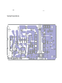
LOCATION OF PCB BOARDS˖
˖
Z N V[O $\N$
]\ dR_$ O$ \N
Y\N QR_
b‘O8\ X$$O \N
S_ \ [a$$O \N _
VERSION VARIATIONS
Type/Versions
Board in used
DVP3850
K/55
KX/77 KG/78
DVP3820
K/93
K/96
K/98
KX/78
Main Board
C/M
C/M
C/M
C/M
C/M
C/M
C/M
Front Control Board
C/M
C/M
C/M
C/M
C/M
C/M
C/M
Power Board
C/M
C/M
C/M
C/M
C/M
C/M
C/M
M
M
M
M
M
M
M
Karaoke+USB Board
*C:Component Level Repair
*M:Module Level Repair
*X:Used
2-1
Mechanical and Dismantling Instructions
Dismantling Instruction
Detailed information please refer to the model set.
The following guidelines show how to dismantle the player.
Step1: Remove 5 screws around the Top Cover, and then remove the Top Cover (Figure 1).
The sample is DVP3850K/98.
Figure 1
Step2: If it is necessary to dismantle Loader or Front Panel, the Front door should be removed first. (Figure 2)
Note: Make sure to operate gently otherwise the guider would be damaged.
Please kindly note that dismantle
the front door
assembly carefully to avoid damage tray and the front door.
Figure 2
2-2
Mechanical and Dismantling Instructions
Detailed information please refer to the model set.
Dismantling Instruction
Step3: If the tray can’t open in normal way, you can make it through the instruction as below (Figure 3).
Note: Make sure to operate gently otherwise the guider would be damaged.
Figure 3
Step4: Dismantling Front Panel, disconnect the connectors (XP82, XP7,XP476), need release 4 snaps of Front Panel & 2 snaps
of bottom cabinet , then gently pull the Panel out from the set. (Figure 4 - Figure 6)
e]?
e ]A
e]
e] A
e]E?
e]@
Figure 4
e] D
2-3
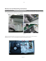
Mechanical and Dismantling Instructions
Dismantling Instruction
Detailed information please refer to the model set.
Step5: Dismantling Loader, disconnect the 3 connectors (XP2, XP3, XP4) aiming in the below figure, and remove 1 screw that
connects the loader and the bottom cabinet. (Figure 5)
Figure 5
Step6: Dismantling Main Board, first disconnect the connector (XP1), and then remove 4 screws. (Figure 6)
Step7: Remove the 4 screws on Power Board to dismantle the Power Board. (Figure 6)
Figure 6
3-1
6RIWZDUHXSJUDGH Preparation to upgrade software
1) Start the CD Burning software and create a new CD
project (Data Disc) with the following setting:
B. Read out the software versions to confirm upgrading
Label: DVP3XXX (No need the label name)
File Name: DVPXXXX_XX.BIN
Power on the set and open the tray, then press <option>
to check the File Name.
1) Power on the set and press <Setup> button on the
remote control.
2) Press <Next><Next><Prev><Prev> button.
The software version and other information are display
Note: It is required capital letter for the File System
on the TV screen as follows:
name.
Version
2) Burn the data onto a blank CDR
SUB-VER XX.XX.XX.XX (software version of
XX.XX.XX.XX (Main version)
application software)
A. Procedure for software upgrade:
8032 XX.XX.XX.XX
1) Power on the set and insert the prepared Upgrade
Servo XX.XX.XX.XX (software version of servo)
CDR.
RIS XX.XX.XX.XX
2) The set will starts reading disc & response with the
DSP XX.XX.XX.XX
following display TV screen:
Region Code X
Upgrade File DETECTED
Upgrade?
Press Play TO START.
3) Press <OK> button to confirm, then screen will display :
Files coping…
UPGRADING…
4) The upgraded tray will automatically open when files
coping complete, then take out the disc.
5) About 1 minute later, the trace will automatically close
when upgrading complete.
Caution: The set must not be power off during
upgrading, Otherwise the Main board will be
damaged entirely.
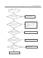
Trouble shooting chart
4-1
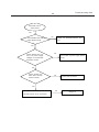
Spindle motor does not move
Motor no move
Go
Check the FFC connection
No
Correct connection
between 24P and the loader.
Yes
No
Check whether “M5V”
Check the M5V power supply
(+5V) voltage is normal.
Yes
Check whether laser voltage
No
(1.9V for CD & 2.4V for DVD)
Check/Replace Q103,Q104.
on L101(R35) and L102(R32)
Yes
1.Whether voltage on pin14/pin15 of U1
varies
between
2.4V
and
3.3V
No
(PIN14=2.4V and PIN15=3.3V for CD;
Check/ Replace U1.
PIN14=3.3V and PIN15=2.4V for DVD),
2.Whether peripheral components are
eroded or badly soldered.
Yes
1.
Check opu focus
No
Check U1 18pin FOCUS_PWM
signals
2.
If there are F+, F-, T+ and T-
signals output from U10.
Yes
FOCUS_PWN waveform
Check/Replace the loader
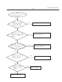
Trouble shooting chart
4-2
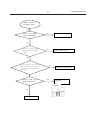
The power can not be on or off
The power can’t be
on or off
Go
Check the power supply
No
on the power board is
Repair the power board
normal.
Yes
Check if the XS301 on the
front board to XP82 on the
Yes
No
Check/Correct
connection
decoder board is in good
contact.
Yes
Whether the connection
No
to K303 is broken.
Correct the connection
Yes
Whether there is 0V and
3.3V voltage difference on
Pin 95 PCON of U1.
Yes
No
Replace U1.
4-3
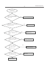
All output voltages on the power board is 0V or deviated.
Trouble shooting chart
All output voltages on
the power board is 0V or
deviated
Yes
Check whether
Yes
Replace F501
F501 is blown
No
Check whether there is
Replace C501&C502 if D501, D502,
No
D503, D504 are normal.
300V on C501 or C502.
Yes
Check whether 100KHz
oscillating signal on
Pin4 of U1
No
Check/ replace U1.
U1(PIN 4 - Drain waveform)
Yes
Check if +5V and +12V are
short.
Yes
Check whether the components in the
short-circuit voltage are defected or eroded.
No
Check whether U1 are eroded.
Trouble shooting chart
4-4
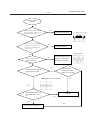
Disc cannot be read.
Disc cannot be read.
Yes
Check the FFC connection
No
Check the loaded circuit
between 24P and the loader.
Yes
1. Whether voltage on pin14/pin15 of U1
Check whether there is laser voltage
No
(1.9V for CD and 2.4V for DVD) on
varies between 2.4V and 3.3V (PIN14=2.4V
and PIN15=3.3V for CD;PIN14=3.3V and
PIN15=2.4V for DVD),
L101(R35) and L102(R32)
2.Check whether peripheral components are
eroded or defect
Yes
Check
U1,
U10,
and
No
peripheral components are
Re-solder or replace the defective parts
eroded or badly soldered.
Yes
Check if there is RFO signal on
pin17 of XP2. (The normal RFO
No
Check U1 and peripheral components
signal is a clear reticulated wave)
Yes
Check the connection
between U1
Yes
Replace U1 or loader.
No
Correct connection
Trouble shooting chart
4-5
Only DVD disc or only disc except DVD can be played
Only DVD disc, or only disc
except DVD can be Played.
Go
Check
the
FFC
connection between
24pin and the loader.
No
Check the loaded circuit
Yes
Check whether there is laser
DVD)
on
L101(R35)
Check the solder status on U1 and
No
voltage (1.9V for CD and 2.4V for
peripheral components
and
L102(R32).
Yes
Whether voltage on pin14/pin15 of U1
No
varies between 2.4V and 3.3V (PIN14
=2.4V
and
PIN15=3.3V
for
check if bad solder exist on U1 and
peripheral components
CD;
PIN14=3.3V and PIN15=2.4V for DVD)
Yes
Check whether pins of U1 and
peripheral
components
No
are
Replace the bad spare parts
badly soldered, defected
Yes
Check Q103, Q104
whether in good
condition
Yes
Change U1 or the loader.
No
Correct connection
Trouble shooting chart
4-6
No display on LED, and buttons do not work
No display on LED, and
buttons do not work
Yes
Check whether there is
correct
contact
between
No
Correct connection
XS301 and XP82
Yes
Check VCC(M5V) voltage
Fix power supply board top
a power supply for should
electric circuit
No
on the power and front
board
Yes
Check there are STB, SDA
Check the U1’s pin 34,35,39 arrive
No
the XP82 connect condition
and SCK signals on XS301
on the front board.
XP82 (PIN 4 CLK)
XP82 (PIN6 DOUT)
Yes
1.Check whether bad solder exists on
U301 and pins of LED,
2.Check whether the circuit connected to
K302, K303 and K301 is broken,
3.Check whether R1, R3 on front board
and R81,R82 and R83 on MEPG board
are open-circuit.
Yes
Replace U301 or LED
No
Correct connection
Trouble shooting chart
4-7
Distorted audio and loud noise
Distorted audio and
loud noise
Yes
Check the power supply voltages
M5V to the operation amplifying
No
Check Q544
Q544 is normal.
Yes
No
Check whether the muting resistance
R369,R375 are normal
Replace R369,R375
Yes
Check
whether
transistor
the
Q361,Q362
No
muting
Replace Q361,Q362
are
normal
Yes
Checking the U361 leads
No
the feet has no to break to
open
&RUUHFWFRQQHFWLRQ
Yes
No
Check the voltage on
pin3 or pin5 of U361 is
Replace R362,R363
OK.
(Should be 2.5~3.1V)
Yes
Check whether the U1 or
U361 powersupply normal
Yes
Replace U1 or U361
No
Check U361
Trouble shooting chart
4-8
Abnormal color of video picture
Abnormal color of
video picture
Yes
Check whether the 27MHz
No
Check Y2, R12,R34,R16,C10 and
output signal normal.
C11
Yes
Check whether the 3.3V
and 1.2V power supply
voltages on the decoder
board are normal.
No
Check other of power supply electric
circuit
Yes
Check whether the
video filter network
circuit is normal.
No
Correct the connection
Yes
Check if the video signals on Pin
100,102,103,104, of U1 are normal
No
change U1
Trouble shooting chart
4-9
Remote reception is insensitive or fails.
Remote reception is
insensitive or fails.
Go
Check if the remote
control works properly.
No
Check battery
Yes
Check if the power supply
No
Check
voltage to the remote censor
R315ǃC315
is normal
Yes
Use an oscilloscope to check if there is
No
output waveform from the first pin IR of the
REM301(PIN1 - RC waveform)
remote censor after pressing button on the
remote control.
Yes
Check if there is IR
signal on pin 39 of U1
Yes
Change U1
IR waveform
No
Correct connection
Trouble shooting chart
4-10
No video picture, no sound.
No video picture,
no sound.
Check whether all the voltages
No
Check the loaded circuit
from the power board to the
CVBS(R884 point) waveform
decoder board are normal.
Yes
Check if the reset circuit consisting
No
ofCE1,Q1,Q2 is normal (at a low
Change CE1,Q1,Q2.
level for tens of milliseconds, then
constantly at 3.3V).
27Mhz waveform
Yes
Check whether there is
Crystal oscillator Y1 and
No
peripheral components
27MHz signal output.
are defected or eroded.
Yes
No
Check whether
short-circuit or bad
solder on U176,U186
Check if there is 135MHz
signal output on R193.
SDRAM(R193 DCLK) waveform
No
Yes
Check if short-circuit and
bad solder exist on Pin
72
Check U1.
No
Yes
Yes
Reconnect the component in
5-1
5-1
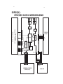
DVP385(X):
MTK1389J BLOCK & WIRING DIAGRAM
P441
R
COAX
L
P1
Pr
Y
Pb
CVBS
1
XP1
XS201
5PIN*2.5
5
5PIN*2.5
AM5888
MOTER
DRIVER
6
16M
FLASH
1
5PIN*2.0
1
8PIN*2.0
5
1
XP80
8
4PIN*2.0 4
XP476
XP71
MIC
DV33
IR
5V
GND
DATA
STB
CLK
POWER_K
+5V
GND
GND
3
MAIN BOARD
+12VA
LOADLOAD+
OUTSW
GND
INSW
GND
+12V
GND
M5V
M5V
1
6PIN*2.0
XP3
SPSP+
HOMESW
GND
SLSL+
POWER
SUPPLY
1
5
64M/16M
SDRAM
XP2
24PIN*0.5
VIDEO LPF
MT1389J
24
1
XP4
ASA 8829F LOADER+
IM RFXP2
DVD LOADER
AUDIO
AMP&LPF
USB_DM
USB_DP
8
1
XS301
8PIN*2.0
LED DISPLAY+ET6202
(LED229GA3JY)
7
1
XP601
7PIN*2.0
KOK+USB
6-1
6-1
5
4
3
2
1
Front Control Board Circuit Diagram:
5V
D
D
R316
)5200$,1%2$5'
XS301
8PIN/2.0mm/140mm
DV33
1 1
IR
IR
2 2
5V
VCC
3 3
4
GND
4
DATA
5
DATA
5
CS
6
CS
6
CLK
CLK
7 7
POWER_K
8
8
R306
51K
R303 R304 R305
4.7K 4.7K 4.7K
U301
DRIVER_LED_ET6202
0R
0R
R307
R308
R309
R310
10K
10K
C301 C302
C303
0.1uF/50V/Y5V
1K
SEG1
1K
SEG2
SEG3
SEG4
SEG5
SEG6
SEG7
CE300
+
47uF/16V
1
2
3
4
5
6
7
8
9
10
11
12
13
14
KEY1
KEY2
100pF/50V/NP0
C300
100pF/50V/NP0
R3
R1
100pF/50V/NP0
DATA
CLK
CS
NC/33 LED-
OSC
DI/O
CLK
STB
KEY1
KEY2
VDD
SEG1/KS1
SEG2/KS2
SEG3/KS3
SEG4/KS4
SEG5/KS5
SEG6/KS6
SEG7/KS7
GND
GRID1
GRID2
GND
GRID3
GRID4
GND
VDD
SEG14/GRID5
SEG13/GRID6
SEG12/GRID7
SEG10/KS10
SEG9/KS9
SEG8/KS8
LED1
GRID[1:5]
28
27
26
25
24
23
22
21
20
19
18
17
16
15
GRID5
GRID4
GRID3
GRID2
GRID1
SEG8
SEG7
SEG6
SEG5
SEG4
SEG3
SEG2
SEG1
GRID1
GRID2
GRID3
GRID4
5V
GRID5
NC/33 LED+
R323
SEG8
13
12
11
10
9
8
7
6
5
4
3
2
1
GRID5
GRID4
GRID3
GRID2
GRID1
SEG8
SEG7
SEG6
SEG5
SEG4
SEG3
SEG2
SEG1
LED_2501AHG1
SEG[1:8]
K301
K302
R312
D301
open/close
1N4148
play/pause
1K
K303
R311
D302
POWER_K
C
power
POWER_K1
C
NC/1K
NC/1N4148
R313 NC/0
DV33
REM301
GND
GND
VCC
GND
IR
IRM_12mm
5V
R315 100
5
4
3
2
1
R318
NC/100
R314
0
IR
+ CE301
NC/47uF
C306
C315
47pF/50V/NP0
1uF/50V/Y5V
consumption
Q1
R317
R319
R321
R322
R323
R316
R313
Y
Y
Y
Y
Y
N
N
N
N
N
N
N
N
Y
Y
DV33
0.3W
R317
1K
1W
Y
LED+
5V
R319
Q1
+
4.7K
LED2
NPN_3DG3904M
CE302
10uF/16V
LED_RED
R321
1K
B
LED-
B
R322
0
A
A
5
4
3
2
1
6-2
6-2
1
2
3
4
5
Karaoke and USB Board Circuit Diagram:
R210
R202
12V
12VA
12VA
REF
CE200
C201
150
A
22K
CE201
A
R211
0.1u
22uF
22uF
R203
C205
47p
R205
180K
22K
2
2.2uF
3
C203
8
R200
10K
ĭ3.5mm
C211
1
C208
100p
2.2uF
NJM4558
5
+
6
-
C204
100p
1000p
REF
NJM4558
MIC_OUT
7
4
5.6K
U200A
8
C210
+
R201
1
2
3
-
KARAOKE
B
47-EAR024-XX0
P601
KARAOKE INPUT
4
100K
B
U200B
12VA
R207
100K
C206
47p
R206
20K
C209
2.2uF
P600
USB
C
C
R208
47-USB003-XX2
USB
1
2
3
4
5
6
VCC
USB_DN
USB_DP
SGND
MGND
MGND
MIC_OUT
MIC
12V
1K
R209
680
VCC
SGND
USB_DN
USB_DP
8PIN/2.0mm
XP601
L200
MGND
1
2
3
4
5
6
7
AGND
500Z
D
D
L201
MGND
AGND
500Z
L202
MGND
SGND
500Z
E
E
1
2
3
4
5
6-3
6-3
A
B
C
D
E
Power Supply Board Circuit Diagram:
1
1
* CAUTION :
THE PARTS MARKED WITH
ARE IMPORTANT PARTS ON THE SAFETY.
PLEASE USE THE PARTS HAVING THE DESIGNATED PARTS NUMBER WITHOUT FAIL.
F501
FUSE_2A250V/2W 10 Ohm
TR501
NTC 10
2
CX501
+
CON502
RV501
VTC 470
OHM
0.1uF/275Vac
+
1
AC INPUT
1
2
+
CN501
+
AC INPUT
D501
D502
1N4007
1N4007
D503
D504
L503
20mH
2
1
L501
680UH
+
C501
10uF/400V
AC INPUT
1N4007
+
C502
15uF/400V
1N4007
FB501
FB
T501
6
2
2
C504
103/400V
R502
300K
5
R503
300K
CON503
D506
5
4
3
2
1
4
D507
FR107
FR102
8
+
GND
+12V
GND
+5V
+5V
C505
47uF/25V
GND
D509
BR
Drain
Drain
2
11
1
2
1
FB
U501
VIP17/VIP27
L502
6.8uH
9
+
C507
1000uF/16V
4
Vdd
CONT
3
2
GND
SB360
1
6X2.5 HEADER
5
7
8
10
+
C508
470uF/16V
R505
12k 1%
R506
22 1/6w
R507
11.3k 1%
1
4
D508
FR102
3
D510
18HSC
U502
PC123X92
R508
1k 1/6w
2
C510
0.1uF/63V
3
R516
22
+
C509
47uF/50V
3
R510
10k 1/6w
U503
TL431
3
R509
220 1/6w
C511
0.1uF/63V
2
1
CY501
1000PF/250VAC
4
4
A
B
C
D
E
6-4
6-4
5
4
3
2
1
Main Board Circuit Diagram: power motor driver
Istandby:21mA
TO POWER BOARD
R751
NM/0
Inor=465mA
5V
M5V
M5V
R761
1.8/2W
Inor=150mA
XP1
5pin/2.5mm
GND
C753
1uF
Q753
SS8550D
GND
50mA
C752
0.1uF/NC
C751
0.1uF/NC
e
M5V
R753
R752
NM/0
Q761
TR_B1
+12V
2.2K
Q751
POWER_K
+5V: +5V(+-2.5%)
+
REG01
C761
0.1uF
0
C762
CE761 REG02
220uF16V
R766
12K 1%
4.7K
IR
VSDA
VSTB
VSCK
4
4
4
4
POWER_K
4
R767
4.7K
R757
IR
VSDA
VSTB
VSCK
DV12
R765
20K 1%
R758
SS8550D
22K
D
Q762
SS8550D
b
SS8550D
R755
+12V: +12V(+-10%)
TR_B2
DV33
c
1
2
3
4
5
R762 10/1W
Inor=315mA
D
Istandby:8mA
+5V
USB_CON
+ CE762
100uF16V
0.1uF
Vref = 1.235--1.27V
modify
PCON
R756
PCON:
L: STBY
H: Working
PCON
4
1K
PCON
Q752
GND
USB_CON
GND
USB_CON
8
BT3904
RFV33
R754
DV33
4.7K
RFV33
4
DV33
4,5
DV33
M5V
R1
5V
R7
R84
4.7K
0R
4.7K
C83
100pF
C85
0.1uF/NC
R86
TO FRONT PANEL
C84
0.1uF/NC
0R/NC
XP82
DV33
C
IR
R80
VSDA
VSTB
VSCK
POWER_K
R88
R81
220R
R82
R83
8
7
6
5
4
3
2
1
100R
220R
220R
1k
C80
C81
C86
100pF/NC100pF/NC0.1uF
01UOPUIFC-101
C82
100pF/NC
TROPEN
TRCLOSE
FMSO
TRSO
DMSO
FOSO
M_BIAS
STBY
TRIN
TROUT
LIMIT
SPSP-A
TROPEN
TRCLOSE
FMSO
TRSO
DMSO
FOSO
M_BIAS
STBY
TRIN
TROUT
LIMIT
SPSP-A
4
4
4
4
4
4
4
4
4
4
4
4
4
MOTOR I/F
B
M5V
A
B
C
D
E
F
RFO
VREF_OPU
LDO_CD
LDO_DVD
LDSW
U10
TT+
SL+
SLR117
1K 1%
5V
L100
2.2R
+
C100
CE100
0.1uF/25V 100uF/16V/NC
24PIN/0.5mm
XP2
GND
GND
FMSO
RESET_A
C105
TR_B2
+
0.1uF/25V
TRSO
CE104
M_BIAS
100uF/16V
STBY
5V_HFM
MDI
LD-CD
VR_DVD
VR_CD
G2
22
23
24
25
26
27
28
GND
VINLD
NC
TRB2
VINTK
BIAS
MUTE
14
13
12
11
10
9
8
G1
29
REV
FWD
REGO1
VINSL+
REGO2
TRB1
VINFC
7
6
5
4
3
2
1
F+
FSPSP+
LOAD+
LOAD-
M5V
TROPEN
TRCLOSE
OPU I/F
REG01
DMSO
REG02
TR_B1 R113
FOSO 10K
RESET_A
RESET_A
4
AM5890
C103
0.1uF/25V
1
1
C101
1000pF
C102
1000pF
SPSP-A
TROPEN
TRCLOSE
FMSO
TRSO
DMSO
FOSO
M_BIAS
STBY
TRIN
TROUT
LIMIT
R114
10K
LDO_DVD
Q103
3CG9012M
C104
R106
4.7
RFV33
C107
0.1uF/25V
NM/1000pF
R107
4.7
Q104
3CG9012M
R134
10K
SP-A
SP+
LIMIT
CE101
47uF/16V
4
4
TROPEN
4
TRCLOSE
4
FMSO
TRSO
DMSO
FOSO
M_BIAS
STBY
TRIN
TROUT
LIMIT
4
4
4
4
4
4
4
4
4
B
MOTOR I/F
A
B
C
D
E
F
RFO
VREF_OPU
LDO_CD
LDO_DVD
LDSW
MDI
VR_DVD
VR_CD
A
B
C
D
E
F
RFO
VREF_OPU
LDO_CD
LDO_DVD
LDSW
4
4
4
4
4
4
4
4
4
4
4
MDI
VR_DVD
VR_CD
4
4
4
OPU I/F
GND
R115 SL1K SL+
1
2
3
4
5
6
1
2
3
4
5
6
1
2
3
4
5
1
2
3
4
5
LOAD-
R116
10K
R118
1K
LOAD+
TROUT
C110
0.1uF/25V
A
R119
1K
TRIN
XP4
5PIN/2.0mm
XP3
6PIN/2.0mm
C108
C109
100pF/NC 100pF/NC
+
CE102
47uF/16V
LDO_CD
5
SPSP-A
DV33
R32
0
R35
L101L102
0 10 UH/NC
10 UH/NC
2
F
B
A
RFO
LDSW
D
C
TT+
F+
F-
30
VOFC+
VOFCVOSLVOSL+
VOTR+
VOTRVCC
4
4
4
4
4
4
4
4
4
4
4
8PIN/2.0mm
DV33
R111
0R
2
E
5V_OPU
VREF_OPU
VOTK+
VOTKVOLD+
VOLDVCC2
NC
VCTL
C106
R112 0.1uF/25V
10K
LD-DVD
26
25
1
2
3
4
5
6
7
8
9
10
11
12
13
14
15
16
17
18
19
20
21
22
23
24
+
A
1
2
3
4
5
6
7
8
9
10
11
12
13
14
15
16
17
18
19
20
21
22
23
24
R120
3K
15
16
17
18
19
20
21
A
B
C
D
E
F
RFO
VREF_OPU
LDO_CD
LDO_DVD
LDSW
C
8
7
6
5
4
3
2
1
4
3
2
1
6-5
6-5
5
4
Main Board Circuit Diagram:MT1389J LQFP 128
Unit Name
Unit Number
Reference
Description
Date&VER
3
2
circuit
Unit Name
Unit Number
Reference
Description
Date&VER
01UURESET-101
A02
1-9
2N3904(89L/R/M/ZR)
2009-06-18
DV33
SP-
R31
circuit
01UCRYSTA-501
A18
10-19
27MHz Crystal(MTK)
2009-06-18
Crystal
R12
100K
OP-
10k
1
Y2
C44
0.1uF
R27
1
D
C45
0.1uF
1
DV33
D20
BAT54C
2
SP-A
XI
R10
3
R3
NC/15K
R5
NC/3.3K
0
RESET_A
R8
27K
URST#
XO
R16
51
3
C11
33pF
URST#
27MHz
OFF-PAGE CONNECTION
C10
33pF
C14
NM/15pF
OPO
R30
10k
Q1
NC/3904
Q2
NC/3904
R6
NC/3.3K
R9
1K
+
Put these circuits as
closer as possible to
MPEG DECODER.
01UURESET-101
CE1
10uF/16V
DQ[0..15]
C1
0.1uF
MA[0..11]
DQM[0..1]
FOR MTK PLATFORMS.
R4
NC/4.7K
DVCC3
C23
C26
DRAM I/F
Digital
C31
BA[0..1]
DCLK
RAS#
CAS#
WE#
CKE
DV33
RESET Circuitry for MTK&ZORAN(
0.1uF 0.1uF 0.1uF
SF_CK
SF_CS
SF_DI
SF_DO
Close to 8202RX-D
DQ[0..15]
D
5
MA[0..11]
5
DQM[0..1]
5
BA[0..1]
5
DCLK
RAS#
CAS#
WE#
CKE
5
5
5
5
5
SF_CK
SF_CS
SF_DI
SF_DO
5
5
5
5
V_CVBS
V_R/V
V_G/Y
V_B/U
7
7
7
7
S-FLASH
M_BIAS
C
RF3.3V
RF +3.3V
C27
LIMIT
R20
4.7
AD_VCC3
C30
1uF
TROUT
LDSW
Internal AD +3.3V
TROPEN
DVDVR R36
CDVR R37
0
0
A
D
F
E
RFV12-2
RF3.3V
51
VR_DVD
VR_CD
XI R34
XO
Close to MT1389J
VREF_OPU
M_BIAS
TRCLOSE
MDI
LDO_CD
LDO_DVD
Anolog_VCC3
DMO
FMO
CDVR
DVDVR
TRO
FOO
TRIN
USB_DM
USB_DP
USB_V33
Standby 8mA
FB22
0R
VVCC3
C33 C32
Video DAC +3.3V
CE23
0.1uF0.1uF
47uF16V
R21
0
AVCC3
CE24
Internal DA +3.3V
C36
Rvrt
R22
220uF6.3V 0.1uF
B
0.1uF
R23
R24
R25
R26
C46 C20 C21
330pF 330pF 0.1uF
27k
27k
15k
10k
FOO
TRO
FMO
DMO
Rvrt close to IC PIN
RFC
RFD
RFE
RFF
AVDD12_2
AVDD33_1
XTALI
XTALO
AGND33
V20
V14
REXT / GPO5
MDI1
LDO1
LDO2
AVDD33_2
DMO
FMO
TRAY_OPEN
TRAY_CLOSE
TRO
FOO
FG / GPIO2
USB_DM
USB_DP
VDD33_USB
VSS33_USB
PAD_VRT
VDD12_USB
SF_CS_
SF_DO
SF_DI
MT1389J
No EPAD
LQFP 128
V1.0
C22
0.015uF
AKIN1
AUDIO_MUTE
SPDIF
96
95
94
93
92
91
90
89
88
87
86
85
84
83
82
81
80
79
78
77
76
75
74
73
72
71
70
69
68
67
66
65
0.1uF
USB_DM
USB_DP
RAS#
CAS#
DVCC3
DQM1
DQ8
DQ9
DQ10
DQ11
DQ12
STBY
TROPEN
TRCLOSE
TRIN
TROUT
SPSP-A
LIMIT
MT1389J
MTK1389L/K-128
M_BIAS
VSTB
POWER_K
VCC1.2
IR
0.1uF
USB_V12
STBY
TROPEN
TRCLOSE
TRIN
TROUT
A
B
C
D
E
F
RFO
VREF_OPU
LDO_CD
LDO_DVD
LDSW
3
3
3
3
3
SPSP-A
3
3
LIMIT
3
FOSO
TRSO
FMSO
DMSO
3
3
3
3
M_BIAS
3
SD33
DV33
5
3,5
RFV33
3
MDI
VR_DVD
VR_CD
DV33
XP8
4pin/2.0mm
0.1uF
MDI
VR_DVD
VR_CD
3
3
3
B
OPU I/F
3
VSDA
3
VSTB
3
POWER_K
3
SD33
DV33
RFV33
USB_CON
USB_CON
3,8
3
PCON
3
01U0RS232-301
A
1
2
3
4
RXD
TXD
RFV12-2
C252 C251
RFV12-1
100pF/NC
100pF/NC
C41
5
3
3
3
3
3
3
3
3
3
3
3
USB_V12
C40
A
C42
10uF/6.3v
A
B
C
D
E
F
RFO
VREF_OPU
LDO_CD
LDO_DVD
LDSW
POWER
PCON
0.1uF
VSCK
IR
C48
Close to MT1389J
8
8
VCC1.2
VSDA
0.1uF
USB_DM
USB_DP
SERVO I/F
VSCK
C35
AUDIO_MUTE 6
SPDIF
6
WE#
MA4
MA5
MA6
MA7
MA8
MA9
MA11
DCLK
DV12
C34
8
USB I/F
DQ4
DQ5
DQ6
DQ7
DQM0
DQ15
DQ14
DQ13
DQ0
DQ1
DQ2
DQ3
SF_CK
VSCK
VSDA
RXD
TXD
URST#
IR
STBY
TROPEN
VSTB
USB_V33
C39
AKIN1
C
VCC1.2
BA1
BA0
FOSO
TRSO
FMSO
DMSO
POWER_K
2.2R
6
6
AUDIO I/F
VVCC3
PCON
CKE
SPDIF
MA3
MA2
MA1
MA0
MA10
M_BIAS
FB24
AL
AR
DVCC3
DACVDDC
GPIO33
GPIO10
SPDIF / GPIO12
RA3
RA2
RA1
RA0
RA10
DVDD12
BA1
BA0
DVDD33
RAS#
CAS#
DVSS12
RWE#
RA4
RA5
RA6
RA7
RA8
RA9
RA11
RCLK
DVDD33
DQM1
RD8
RD9
RD10
RD11
RD12
33
34
35
36
37
38
39
40
41
42
43
44
45
46
47
48
49
50
51
52
53
54
55
56
57
58
59
60
61
62
63
64
FOSO
TRSO
FMSO
DMSO
Anolog_VCC3
C37
C38
4.7uF
C38Ў0805ᇕ㺙ϡ㛑ᬒᑩሖ
5.1k 1%
USB_V12
SF_CS
SF_DO
SF_DI
1
2
3
4
5
6
7
8
9
10
11
12
13
14
15
16
17
18
19
20
21
22
23
24
25
26
27
28
29
30
31
32
RFB
RFA
RFH / OPINN
RFG / OPINP
RFIN / OPOUT / GPI36
RFIP
AGND12
AVDD12_1
ADACVDD2
ADACVDD1
ALF / CENTER / GPIO
ALS / GPIO
AL / GPIO1
AVCM
AR / GPIO0
ARS / GPIO
ARF / LFE / GPIO
ADACVSS1
ADACVSS2
AADVDD
AKIN1 / GPIO21 / Audio_Mute
ADVCM / GPIO20
AKIN2 / GPIO19 / Audio_Mute
AADVSS
R
B
G
DACVDDB
CVBS
DACVSSC
FS
VREF / GPO14
U1
SF_CK
UP1_6 / SCL
UP1_7 / SDA
GPIO11
GPIO6
PRST#
IR
GPIO3 / INT#
GPIO4
GPIO13
GPIO9
GPIO8
GPIO7 / CKE_
GPIO29
GPIO30
GPIO31
GPIO32
DVSS33
DVDD33
RD0
RD1
RD2
RD3
DVDD12
RD4
RD5
RD6
RD7
DQM0
RD15
RD14
RD13
Close to MT1389J
AL
AR
128
127
126
125
124
123
122
121
120
119
118
117
116
115
114
113
112
111
110
109
108
107
106
105
104
103
102
101
100
99
98
97
0.1uF
VIDEO I/F
FS
AUDIO_MUTE
RFV33
0R
R33
560
TP63
GPIO19
V_R/V
V_B/U
V_G/Y
VVCC3
V_CVBS
RF Reference
FB21
TP62
GPIO20
AD_VCC3
AKIN1
+ CE26
47uF/6.3v
C47
C43
0.1uF
AVCC3
+ CE25
47uF/6.3v
V_CVBS
V_R/V
V_G/Y
V_B/U
AL
AVCM
AR
VREF_OPU
RFO
SD33
RFV12-1
FB500R
B
C
OPOPO
TROUT
C50
1uF
FB20
10uF/6.3v
SDRAM +3.3V
close to 89J IC
0.1uF
4
3
2
1
6-6
6-6
5
4
3
2
1
Main Board Circuit Diagram: SDRAM,FLASH
4
SD33
U186
D
MA0
MA1
MA2
MA3
MA4
MA5
MA6
MA7
MA8
MA9
MA10
MA11
DBA0
DBA1
23
24
25
26
29
30
31
32
33
34
22
35
20
21
A0
A1
A2
A3
A4
A5
A6
A7
A8
A9
A10/AP
A11
BA0/A13
BA1/A12
SDCLK
SDCKE
38
37
CLK
CKE
DCS#
DRAS#
DCAS#
DWE#
19
18
17
16
CS
RAS
CAS
WE
DQM0
DQM1
15
39
DQML
DQMH
36
40
NC
NC
54
41
28
VSS
VSS
VSS
DQ0
DQ1
DQ2
DQ3
DQ4
DQ5
DQ6
DQ7
DQ8
DQ9
DQ10
DQ11
DQ12
DQ13
DQ14
DQ15
2
4
5
7
8
10
11
13
42
44
45
47
48
50
51
53
VCC
VCC
VCC
1
14
27
VCCQ
VCCQ
VCCQ
VCCQ
3
9
43
49
VSSQ
VSSQ
VSSQ
VSSQ
6
12
46
52
DQ0
DQ1
DQ2
DQ3
DQ4
DQ5
DQ6
DQ7
DQ8
DQ9
DQ10
DQ11
DQ12
DQ13
DQ14
DQ15
C186
C187
C188
0.1uF
0.1uF
0.1uF
DQ[0..15]
DQ[0..15]
4
4
4
4
MA[0..11]
BA[0..1]
DQM[0..1]
DCLK
4
4
4
CAS#
RAS#
WE#
MA[0..11]
BA[0..1]
DQM[0..1]
DCLK
CAS#
RAS#
WE#
SD33
C189
D
SD33
4
DRAM
0.1uF
SD33
R194
10K
SDCKE
R195
10K
DCS#
SF_CK
SF_CS
SF_DI
SF_DO
DV33
33 CKE
R196
CKE
SD33
4
DRAS#
DCAS#
DWE#
DV33
3,4
RAS#
CAS#
WE#
DBA0
BA0
DBA1
BA1
SDCLK
4
4
4
4
S-FLASH
SD33
SDCKE
SF_CK
SF_CS
SF_DI
SF_DO
R193
33
DCLK
ESMT M12L64164A-7T
SDRAM64M
C190
10pF/NC
C
C
DV33
R182
10K
R181
10K
R184
10K
U176
AT25FS040/EN25B80
SF_CS
SF_DO
1
2
3
4
R183
B
CE# VDD
SO HOLD#
WP# SCK
VSS
SI
8
7
6
5
C176
SF_CK
SF_DI
0.1uF
4M/8M/16M bits
B
10K/NC
01U0FLASH-101
Note 2:IF use R183,Must take over R181.Default use R183(10K),and R181 Open.
A
A
5
4
3
2
1
6-7
6-7
5
4
3
2
1
Main Board Circuit Diagram: AUDIO I/F
01UAUIFTN-501
Range :441-450
D
D
P441
RCA/AUDIO OUT
C442
1000pF
C443
1000pF
C441
47pF/NC
C930
100pF
01UAAMP6H-201
30K 1%
R366
C365
RCA
47-RCA151-XX
1
2
3
4
5
6
CVBS_O
COAXIAL
LCH
RCH
01UAUIFTN-401
6CH Audio AMP for single input
100pF
C452 0.1uF
SPDIF
4
5.1K 1%
2
1
0.1uF REFA
C362
CE363
3
U361A
LM4558
8
C364
10uF16V
+
R365
10K 1%
+
R364
-
AL
R368
LCH
R452
100
470
+12VA
Q361
2N3904
Audio Ampifier Circuit.
R372
Output Interface Circiut for SPDIF Coaxial.
01USPDIFT-101
Range :451-460
30K 1%
C
C367
C451
100pF
A_MUTE R369
10K
+12VA
0.1uF
COAXIAL
100
R367
1500pF
C631
470
R451
100pF
01UMAMPMU-201
5.1K 1%
6
REFA
CE364
7
5
8
C366
+
R371
10uF16V R374
470
AR
AL
AUDIO_MUTE
SPDIF
4
4
4
4
AUDIO I/F
4
10K 1%
Range :541-560
RCH
M5V
+
R370
-
AR
C
AR
AL
AUDIO_MUTE
SPDIF
U361B
LM4558
Q544
R373
10K
1500pF
+12VA
A_MUTE R375
470
A_MUTE
9012
CVBS_O
CVBS_O
7
Q362
2N3904
VIDEO I/F
R548
R550
4.7K
Audio Ampifier Circuit.
22K
R549
4.7K
Q545
9012
R547
CE541 +
+12VA
+12V
R361
100
+12VA R362
+
CE361
100uF25V
3.3K
CE362
R363
10K
220uF16V
REFA
36K
+
100uF16V
AUDIO_MUTE R545
4.7K
Q543
2N3904
R546
B
B
POWER Ciucuit of OP AMP
22K
POP Noise Cancel Circuit For Power On and Power Off.
A
A
5
4
3
2
1
6-8
6-8
5
4
3
2
1
Main Board Circuit Diagram: VIDEO I/F
D
D
01UVIDEOO-101
Range
01UVIDEOT-101
˖
V_CVBS
V_G/Y
V_B/U
V_R/V
CVBS_O
Range ˖
VIDEO OUTPUT TERMINAL.
L881
V_R/V
0R/1.8uH
V_CVBS
V_G/Y
V_B/U
V_R/V
CVBS_O
4
4
4
4
6
VIDEO I/F
R/V_O
P1
RCA/VIDEO OUT
C881
100pF
1
2
3
4
5
6
CVBS_O
G/Y_O
B/U_O
R/V_O
C926
C927
100pF
C928
100pF
RCA
47-RCA150-XX1
R881
75R 1%
C929
100pF
100pF
L882
V_G/Y
C
R882
75R 1%
0R/1.8uH
G/Y_O
C
C882
100pF
B/U_O
R/V_O
G/Y_O
U926
L884
V_CVBS
R884
75R 1%
PESD5VL4BGA
C883
100pF
2
R883
75R 1%
D926
1uH
CVBS
D927
D928
D929
PESD5V0S1BA
1
1
3
2
CVBS_O
B/U_O
PESD5V0S1BA
0R/1.8uH
2
R/V_O
2
L883
V_B/U
PESD5V0S1BA
4
CVBS_O
1
B/U_O
2
5
1
1
PESD5V0S1BA
G/Y_O
NOTE1:D926,D927,D928,D929 only for 94/55/77/78(ie.India/Latin America /Argentine/Brazil) stroke,Other Stroke use U926
C884
100pF
Video Output Circuit.
B
B
Note:Only CE61(470uF/6.3V) use for India stroke.unless other use R230(0 OHM)
R887
0/NC
5V
R888
2.4K
CE882
CVBS
Q884
2N3904
+
47uF/16V
R886
+
3
C885
D884
R889
BAT54S/NC
2.4K
CE883
100pF
2
1
75R 1%
5V
CVBS_O
470uF6.3V/NM
R900
75
A
A
5
4
3
2
1
6-9
6-9
5
4
3
2
1
Main Board Circuit Diagram: KOK & USB I/F
range :221-230
01UKUSBIFT-101
M5V
D
F221
USB_CON
01UKOKIFT-201
range :476-480
Karaoke input interface with MPEG IC,for ZORAN platforms.
FUSE(500MA)
R221
180
R222
180
PBSS5320
Q221
D
VCC_USB
USB_DM
USB_DP
1
2
3
4
C221
D9
ESD0603
C49
AKIN1
R477
1uF
MIC
100
+12VA
C478
0.1uF/NC
C479
3300pF
D10
0.1uF
XP7
USB CONNECTOR
ESD0603
1
2
3
XP476
3PIN*2.0mm
USB HOST Interface and Control Circuit.
Note:Q221 use PBSS5320(BJT teansistor) after Year 2009.
C
C
USB_DP
USB_DM
USB_CON
USB_DP
USB_DM
4
4
USB_CON
3
USB Interface
AKIN1
AKIN1
4
B
B
A
A
5
4
3
2
1
6-10
5
6-10
4
3
2
1
Main Board Circuit Diagram: POWER FLOW
D
D
Switch
<50mA
Power Board
Switch
5V
VFD
+P12V
+12V
VIDEO OUTPUT
M5V
OPU
MPEG Board
C
C
AUDIO AMP CIRCURT
Digital DVCC33
RF +3.3V
3.3V
Internal AD +3.3V
Video DAC +3.3V
1.2V
Internal DA +3.3V
Anolog_VCC3
Motor Driver
USB_V33
MUTE CIRCUIT
SDRAM +3.3V
Serial FLASH +3.3V
USB
IR
STANDBY LED
RESET CIRCUIT
B
B
VCC1.2
USB_V12
RFV12-2
RFV12-1
A
A
5
4
3
2
1
6-11
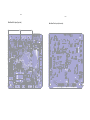
Front Control Board Print-layout (bottom side):
6-11
6-12
6-12
Karaoke and USB Print-layout :
top side:
bottom side:
6-13
6-13
Power Supply Print-layout (bottom side):
6-14
6-14
Main Board Print-layout (top side):
Main Board Print-layout (bottom side):
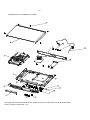
7-1
Exploded view for DVP3850K/55/98:
This is general mechanical exploded view for DVP3850K/55.Please refer to the model set for the detailed information.
ASSY includes components:1,2,4.
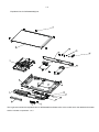
7-2
Exploded view for DVP3850K/77/78/93/96 :
This is general mechanical exploded view .Please refer to the model set for the detailed information.
ASSY1 includes components :1,2,4
7-3
Exploded View for DVP3850KG(X)/78:
This is general mechanical exploded view for DVP3850KG/78.Please refer to the model set for the detailed information.
ASSY1 includes components :1,2,4
8-1
Revision List
γ
γ
Version 1.0
Initial Release for DVP3850K/55.
Version 1.1
Adding DVP3820KX/78 ,DVP3850KX/77
Version 1.2
*Adding DVP3850KG(X) /78,DVP3850K/96/98
Version 1.3
*Adding DVP3850K/93