1
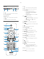
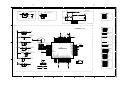
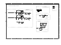
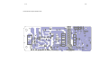
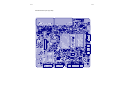
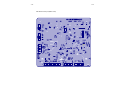
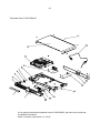
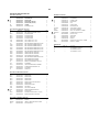
DVP3520 DVP3520/55 Service Manual TABLE OF CONTENTS Page . Technical Specifications…………....………………………..............1-2 . Safety Instruction, Warning & Notes….……………………....….....1-3 . DFU Instruction..............................................................................2-1 . Mechanical and Dismantling Instructions…………........................3-1 . Software Upgrades and Region Code Change..............................4-1 . Trouble Shooting Chart………………………………………………. 5-1 . Wiring Diagram………………………………………..………..….….6-1 . Electrical Diagrams and Print-layouts..….…………………....….…7-1 . Set Mechanical Exploded view & Part list.…………………..….….8-1 . Revision List..................................................................................9-1 ©Copyright 2010 Philips Consumer Electronics B.V. Eindhoven, The Netherlands All rights reserved. No part of this publication may be reproduced, stored in aretrieval system or transmitted, in any form or by any means, electronic, mechanical, photocopying, or otherwise without the prior permission of Philips. Published by SL - 949 BU AVM Version 1.0 Printed in The Netherlands Subject to modification CLASS 1 LASER PRODUCT GB 3141 785 34560 PHILIPS 1-2 Specifications Note • Specification and design are subject to change without notice Video • Signal system: PAL / NTSC • Composite video output: 1 Vpp ~ 75 ohm • Component video output: 0.7 Vpp ~ 75 ohm Audio • Analog stereo output • Signal to noise ratio (1 kHz): > 90 dB (A-weighted) • Dynamic Range (1 kHz): > 80 dB (A-weighted) • Crosstalk (1 kHz): > 80 dB • Distortion/noise: (1 kHz): > 70 dB • MPEG MP3: MPEG Audio L3 • Digital output • Coaxial Main unit • Dimensions (w x h x d): 360 x 39 x 209 (mm) • Net Weight: approximately 1.4 kg Power • Power supply rating: 110 - 240V, 50/60HZ • Power consumption: < 10 W • Power consumption in standby mode: < 1 W Accessories supplied • Remote control and batteries • Audio/Video cables • Power plug adaptor • User Manual Laser specification • Type: Semiconductor laser InGaAIP (DVD), AIGaAs (CD) • Wave length: 656 nm (DVD), 790 nm (CD) • Output Power: 7.0 mW (DVD), 10.0 mW (VCD/CD) • Beam divergence: 60 degrees 1-3 Safety instruction, Warning & Notes Safety instruction 1. General safety 2.Laser safety Safety regulations require that during a repair: . Connect the unit to the mains via an isolation transformer. . Replace safety components indicated by the symbol , only by components identical to the original ones. Any other component substitution (other than original type) may increase risk of fire or electrical shock hazard. Safety regulations require that after a repair, you must return the unit in its original condition. Pay, in particular, attention to the following points: . Route the wires/cables correctly, and fix them with the mounted cable clamps. . Check the insulation of the mains lead for external damage. . Check the electrical DC resistance between the mains plug and the secondary side: 1) Unplug the mains cord, and connect a wire between the two pins of the mains plug. 2) Set the mains switch the “on” position (keep the mains cord unplug). 3) Measure the resistance value between the mains plug and the front panel, controls, and chassis bottom. 4) Repair or correct unit when ¡ measurement is less than 1M . the resistance 5) Verify this, before you return the unit to the customer/user (ref. UL-standard no. 1492). 6) Switch the unit “off”, and remove the wire between the two pins of the mains plug. This unit employs a laser. Only qualified service personnel may remove the cover, or attempt to service this device (due to possible eye injury). Laser device unit Type : Semiconductor laser GaAlAs Wavelength : 650nm (DVD) : 780nm (VCD/CD) Output power : 7mW (DVD) : 10mW (DVD /CD) Beam divergence: 60 degree Note: Use of controls or adjustments or performance of procedure other than those specified herein, may result in hazardous radiation exposure. Avoid direct exposure to beam. 1-4 Warning 1.General 2. Laser . All ICs and many other semiconductors are susceptible to . The use of optical instruments with this product, will electrostatic discharges (ESD). Careless handing during increase eye hazard. repair can reduce life drastically. Make sure that, during . Only qualified service personnel may remove the cover repair, you are at the same potential as the mass of the or attempt to service this device, due to possible eye set by a wristband with resistance. Keep components and injury. tools at this same potential. Available ESD protection with a disc loaded inside the player. equipment: 1) . Repair handing should take place as much as possible Complete kit ESD3 (small tablemat, wristband, connection box, extension cable and earth cable) . Text below is placed inside the unit, on the laser cover shield: 4822 310 10671. 2) Wristband tester 4822 344 13999. . Be careful during measurements in the live voltage section. The primary side of the power supply , including the heat sink, carries live mains voltage when you CAUTION: VISIBLE AND INVISIBLE LASER RADIATION WHEN OPEN, AVOID EXPOSURE TO BEAM. connect the player to the mains (even when the player is “off”!). It is possible to touch copper tracks and/or components in this unshielded primary area, when you Notes: service Laboratories. The double-D symbol is trademarks of Dolby the player. Service personnel must take precautions to prevent touching this area or components in this area. A “lighting stroke” and a stripe-marked printing on the printed wiring board, indicate the primary side of the power supply. . Never replace modules, or components, while the unit is “on”. Manufactured under licence Laboratories, Inc. All rights reserved. from Dolby 1-5 Notes Lead-Free requirement for service INDENTIFICATION: x Regardless of special logo (not always indicated) Use only original spare-parts listed in the Service-Manuals. Not listed standard-material (commodities) has to be purchased at external One must treat all sets from 1.1.2005 onwards, according next rules. companies. x Important note: In fact also products a little older can also be treated in this way as long as you avoid mixing solder-alloys (leaded/ lead-free). So best to always use SAC305 and the higher temperatures belong to this. Special information for BGA-ICs: - always use the 12nc-recognizable soldering temperature profile of the specific BGA (for de-soldering always use highest lead-free temperature profile, in case of doubt) Due to lead-free technology some rules have to be respected by the workshop during a repair: - lead free BGA-ICs will be delivered in so-called ‘dry-packaging’ (sealed pack including a silica gel x Use only lead-free solder alloy Philips SAC305 with order code 0622 149 00106. If lead-free solder-paste is pack) to protect the IC against moisture. After required, please contact the manufacturer of your opening, dependent of MSL-level seen on solder-equipment. In general use of solder-paste within indicator-label in the bag, the BGA-IC possibly workshops should be avoided because paste is not easy still to store and to handle. communicated via AYS-website. to be baked dry. This will be Do not re-use BGAs at all. x Use only adequate solder tools applicable for lead-free solder alloy. The solder tool must be able has x For sets produced before 1.1.2005, containing o To reach at least a solder-temperature of 400°C, leaded soldering-tin and components, all needed o To stabilize the adjusted temperature at the spare-parts will be available till the end of the solder-tip o To exchange solder-tips for different applications. x Adjust your solder tool so that a temperature around 360°C – 380°C is reached and stabilized at the solder joint. Heating-time of the solder-joint should not exceed service-period. For repair of such sets nothing changes. x On our website: www.atyourservice.ce.Philips.com You find more information to: ~ 4 sec. Avoid temperatures above 400°C otherwise BGA-de-/soldering (+ baking instructions) wear-out of tips will rise drastically and flux-fluid will be Heating-profiles of BGAs and other ICs used in destroyed. To avoid wear-out of tips switch off un-used Philips-sets equipment, or reduce heat. x Mix of lead-free solder alloy / parts with leaded solder alloy / parts is possible but PHILIPS recommends You will find this and more technical information within the “magazine”, chapter “workshop news”. strongly to avoid mixed For additional questions please contact your local solder alloy types (leaded and lead-free). If one cannot repair-helpdesk. avoid, clean carefully the solder-joint from old solder alloy and re-solder with new solder alloy (SAC305). 2-1 Main unit a • Turn on the unit or switch to standby. • Open or close the disc compartment. b a b c c DISC MENU • Access or exit the disc menu. • During the play of a photo slideshow, switch between the Fun Mode and Simple Mode. • For VCD and SVCD: turn on or off PBC (playback control). d e a Turn on the unit or switch to standby. b Disc compartment c Display panel d d Open or close the disc compartment. • • Start, pause or resume disc play. • e e Remote control a / • Skip to the previous or next title, chapter, or track. • Mute or restore the volume g h Numeric buttons • Select an item to play. b r i SUBTITLE • Select a subtitle language on a disc. j • • d q e p f g BACK Return to the previous display menu. • f c Navigate the menus. Search fast-forward ( ) or fast-backward ( ). Search slow-forward ( ) or slowbackward ( ). o n ZOOM Fit the picture display to the TV screen. Zoom the picture in or out. k REPEAT • Select various repeat play modes. l REPEAT A-B • Repeat play for a specific section. m AUDIO • Select an audio language or channel on a disc. n • Stop play. • Start, pause or resume disc play. o p h INFO For discs: access the play options or display the current disc status. • For slideshows: display a thumbnail view of photo files. • i m j l k q OK • Confirm an entry or selection. r SETUP • Access or exit the setup menu. 3-1 Mechanical and Dismantling Instructions Dismantling Instruction Detailed information please refer to the model set. The following guidelines show how to dismantle the player. Step1: Remove 5 screws around the Top Cover, and then remove the Top Cover (Figure 1). Figure 1 Step2: If it is necessary to dismantle Loader or Front Panel, the Front door should be removed first. (Figure 2) Note: Make sure to operate gently otherwise the guider would be damaged. Please kindly note that dismantle the front door assembly carefully to avoid damage tray and the front door. Figure 2 3-2 Mechanical and Dismantling Instructions Detailed information please refer to the model set. Dismantling Instruction Step3: If the tray can’t open in normal way, you can make it through the instruction as below (Figure 3). Note: Make sure to operate gently otherwise the guider would be damaged. Figure 3 Step4: Dismantling Front Panel, disconnect the connectors (XS30 1), need release 4 snaps of Front Panel & 2 snaps of bottom cabinet , then gently pull the Panel out from the set. (Figure 4 - Figure 6) XP1 XP2 XP3 XP4 XS301 Figure 4 3-3 Mechanical and Dismantling Instructions Dismantling Instruction Detailed information please refer to the model set. Step5: Dismantling Loader, disconnect the 3 connectors (XP2, XP3, XP4) aiming in the below figure, and remove 1 screw that connects the loader and the bottom cabinet. (Figure 5) Figure 5 Step6: Dismantling Main Board, first disconnect the connector (XP1), and then remove 4 screws. (Figure 6) Step7: Remove the 4 screws on Power Board to dismantle the Power Board. (Figure 6) Figure 6 4-1 Softeware upgrade and region code change Preparation to upgrade software 1) Power on the set and open the tray, then press "5""5" B. Read out the software versions to confirm upgrading on remote control to check the SW File Name. 2) Start the CD Burning software and create a new CD project (Data Disc) with the following setting: Label: DVP3XXX (No need the label name) 1) 2) SW File Name: DVPXXXX_XX.bin Note: It is required to keep the SW file name accord. 3) Burn the data onto a blank CDR Power on the set and press "Setup" button on the remote control. Press "1""3""7""9" button or press down cursor on remote control to select "Preferences" and press right & down cursor to select "Version Info". The software version and other informations will be displayed on the TV screen as follows: Version XX.XX.XX.XX (Main version) Sub-Ver XX.XX.XX.XX (version of applicaton software) A) Upgrade software via CDR: 8032 XX.XX.XX.XX 1) Power on the set and insert the prepared Upgrade CDR. Servo XX.XX.XX.XX (software version of Servo) 2) The set will starts reading disc & response with the RISC XX.XX.XX.XX following display TV screen: DSP XX.XX.XX.XX A. Procedure for software upgrade: Upgrade file detected Region Code X Upgrade ? Press PLAY to start 3) Press "PLAY" button to confirm, then screen will display: Upgrade file detected Do not power off File Copying 4) Upgrade file detected Do not power off Upgrading The upgraded tray will automatically open when file copying completed, then take out the disc. 5) About 1 minute later, the trace will automatically close when upgrading completed. Region Code Change 1) Power on the set and open the tray door; 2) Press the "Setup" button on the remote control, then the setup interface will be displayed on the TV screen; 3) Move the down cursor on remote control to select "Preferences" and press "1""3""8""9""3""1" on the remote control; 4) Then move the up or down cursor to select the region code. Note: Restart after above steps. Caution: The set must not be power off during upgrading, Otherwise the Main board will be damaged entirely. Trouble shooting chart 5-1 Spindle motor does not move Motor no move Go Check the FFC connection No Correct connection between 24P and the loader. Yes No Check whether “M5V” Check the M5V power supply (+5V) voltage is normal. Yes Check whether laser voltage No (1.9V for CD & 2.4V for DVD) Check/Replace Q103,Q104. on L101 and L102 Yes 1.Whether voltage on pin102/pin103 of U1 varies between 2.4V and 3.3V (Pin102=3.3V No and Pin103=2.4V for CD; Pin102=2.4V and Pin103=3.3V for DVD), Check/Replace U1. 2.Whether peripheral components are eroded or badly soldered. Yes Check opu focus No 1. Check U1 111pin FOCUS_PWM signals 2. If there are F+, F-, T+ and T- signals output from U10. Yes Check/Replace the loader FOCUS_PWN waveform Trouble shooting chart 5-2 The power can not be on or off The power can’t be on or off Go Check the power supply No on the power board is Repair the power board normal. Yes Check if the XS301 on the front board to XP5 on the Yes No Check/Correct connection decoder board is in good contact. Yes Whether the connection No to K303 is broken. Correct the connection Yes Whether there is 0V and 3.3V voltage difference on Pin 118 PCON of U1. Yes No Replace U1. 5-3 Trouble shooting chart All output voltages on the power board is 0V or deviated. All output voltages on the power board is 0V or deviated Yes Check whether Yes Replace F501 F501 is blown No Check whether there is Replace C501&C502 if D501, D502, No D503, D504 are normal. 300V on C501 or C502. Yes Check whether 100KHz oscillating signal on Pin6 of U1 No Check/ replace U1. U1(PIN 3 - RC waveform) U1(PIN 8 - Drain waveform) Yes Check if +5V and +12V are short. Yes Check whether the components in the short-circuit voltage are defected or eroded. No Check whether U1 are eroded. 5-4 Trouble shooting chart Disc cannot be read. Disc cannot be read. Yes Check the FFC connection No Check the loaded circuit between 24P and the loader. Yes 1. Whether voltage on pin102/pin103 of U1 Check whether there is laser voltage (1.9V for CD and 2.4V for No varies between 2.4V and 3.3V (Pin102=3.3V and Pin103=2.4V for CD; Pin102=2.4V and Pin103=3.3V for DVD), DVD) on L101 and L102. 2.Check whether peripheral components are eroded or defect Yes Check U1, U2, and No peripheral components are Re-solder or replace the defective parts eroded or badly soldered. Yes Check if there is RFO signal on pin17 of XP2. (The normal RFO No Check U1 and peripheral components signal is a clear reticulated wave) Yes Check the connection between U1 Yes Replace U1 or loader. No Correct connection Trouble shooting chart 5-5 Only DVD disc or only disc except DVD can be played Only DVD disc, or only disc except DVD can be Played. Go Check the FFC connection between 24pin and the loader. No Check the loaded circuit Yes Check whether there is laser No voltage (1.9V for CD and 2.4V Check the solder status on U1 and peripheral components for DVD) on L101 and L102. Yes Whether voltage on pin102/pin103 of No U1 varies between 2.4V and 3.3V check if bad solder exist on U1 and peripheral components (Pin102 =3.3V and Pin103=2.4V for CD; Pin102=2.4V and Pin103=3.3V Yes Check whether pins of U1 and peripheral components are badly soldered, defected No Replace the bad spare parts Yes Check Q103, Q104 whether in good condition Yes Change U1 or the loader. No Correct connection Trouble shooting chart 5-6 No display on LED, and buttons do not work No display on LED, and buttons do not work Yes Check whether there is correct contact between XS301 and XP5 No Correct connection Yes Check VCC(M5V) voltage on the power and front Fix power supply board top a power supply for should electric circuit No board Yes Check there are STB, SDA and SCK signals on XS301 No Check the U1’s pin 1,119,122 arrive the XP5 connect condition on the front board. XP5 (PIN 1 CLK) XP5 (PIN3 DOUT) Yes 1.Check whether bad solder exists on U301 and pins of LED, 2.Check whether the circuit connected to K302, K303 and K301 is broken, 3.Check whether R300, R301 and R302 are open-circuit. Yes Replace U301 or LED No Correct connection 5-7 Trouble shooting chart Distorted audio and loud noise Distorted audio and loud noise Yes Check the power supply voltages M5V to the operation amplifying Q544 is normal. No Check Q544 Yes Check whether the muting No resistance R369,R375 are Replace R369,R375 normal Yes Check whether the muting transistor Q361,Q362 are normal No Replace Q361,Q362 Yes Checking the U361 leads No &RUUHFWFRQQHFWLRQ the feet has no to break to open Yes Check the voltage on pin3 or pin5 of U361 is OK. No Replace R362,R363 (Should be 2.5~3.1V) Yes Check whether the U1 or U361 powersupply normal Yes Replace U1 or U361 No Check U361 5-8 Trouble shooting chart Abnormal color of video picture Abnormal color of video picture Yes Check whether the No Check Y1, R10,R11,C10 and C11 27MHz output signal Yes Check whether the 3.3V and 1.2V power supply voltages on the decoder board are normal. No Check other of power supply electric circuit Yes Check whether the video filter network circuit is normal. No Correct the connection Yes Check if the video signals on Pin 69,73,74,75, of U1 are normal No change U1 5-9 Trouble shooting chart Remote reception is insensitive or fails. Remote reception is insensitive or fails. Go Check if the remote control works properly. No Check battery Yes Check if the power supply voltage to the remote censor is normal No Check R315ǃC315 Yes Use an oscilloscope to check if No there is output waveform from the first pin IR of the remote censor REM301(PIN1 - RC waveform) after pressing button on the remote control. Yes Check if there is IR signal on pin 2 of U1 Yes Change U1 IR waveform No Correct connection 5-10 Trouble shooting chart No video picture, no sound. No video picture, no sound. No Check whether all the voltages CVBS(R21 point) waveform Check the loaded circuit from the power board to the decoder board are normal. Yes Check if the reset circuit consisting of No CE2, D1,Q1 is normal (at a low level for tens of milliseconds, then Change CE2, D1,Q1. constantly at 3.3V). 27Mhz waveform Yes Check whether there is Crystal oscillator Y1 and No peripheral components 27MHz signal output. are defected or eroded. Yes Check if there is 135MHz No Check whether short-circuit or bad solder on U176,U186 signal output on R193. SDRAM(R193 DCLK) waveform No Yes Check if short-circuit and bad solder exist on Pin 69 No Check U1. Yes Yes Reconnect the component in 6-1 5 6-1 4 3 2 1 DVP3520 SPHE8202RQ-D(2ch) WIRING DIAGRAM Pr Y P1 Pb CVBS COAX FR FL AUDIO AMP&LPF 6 LOADLOAD+ OUTSW GND INSW 5PIN*2.0 XP1 6 XP303 4 KS6S KEY2 LED+ LED- 1 XP2 6 B 5V IR GND DATA STB CLK MAIN BOARD SWITCH 4PIN*2.0 BOARD XS201 3PIN*2.5 1 6PIN*2.0 1 4 C 16M serial FLASH MX25L1605 1 5 B +P12V GND M+5V POWER SUPPLY TNY176 5 MOTER DRIVER XP8 SPSP+ HOMESW GND SLSL+ 6PIN*2.0 SPHE8202RQ-D 24 1 1 5 EM6381 64M SDRAM XP4 24PIN*0.5 3PIN*2.5 VIDEO LPF 1 XP9 C TDM-3 LOADER+IM S76RFXP2 DVD LOADER P4 D AM5888 D 1 XS302 XS301 6PIN*2.0 4PIN*2.0 1 LED DISPLAY+ET6202 (LED229GA3JY) A A 5 4 3 2 1 7-1 7-1 5 4 3 Front Board Circuit Diagram: VCC 2 1 U5V R315 REM301 5 )5200$,1%2$5' 4 5 4 VCC GND IR 3 2 1 100 ohm R318 100R/NC IR + REM for dvp352x IR VCC GND DATA CS CLK U5V 1 2 3 4 5 6 7 8 9 10 C306 0.1u C315 47p XS301 D R320 VCC 0R 1 2 3 4 LED+ LEDPOWER_K1 POWER_K U5V STB_LED XS302 CON4(2.0) CE301 47uF C316 100p IR DATA CS CLK C307 100p D C308 100p VCC POWER_K STB_LED 5VL R303 R304 R305 R319 0 ohm LED- CON10(2.0) R306 4K7 DATA CLK CS R300 R301 R302 4K7 51K 4K7 100 100 100 R307 R308 10K 10K C300 C301 C302 C 100P 100P R317 33R R309 R310 5VL 0.1u 1K 1K SEG1 SEG2 SEG3 SEG4 SEG5 SEG6 100P C303 U301 ET6202 1 2 3 4 5 6 7 8 9 10 11 12 13 14 CE300 + OSC DI/O CLK STB KEY1 KEY2 VDD SEG1/KS1 SEG2/KS2 SEG3/KS3 SEG4/KS4 SEG5/KS5 SEG6/KS6 SEG7/KS7 LED1 GRID[1:7] GND GRID1 GRID2 GND GRID3 GRID4 GND VDD SEG14/GRID5 SEG13/GRID6 SEG12/GRID7 SEG10/KS10 SEG9/KS9 SEG8/KS8 28 27 26 25 24 23 22 21 20 19 18 17 16 15 GRID1 GRID2 GRID3 GRID4 GRID5 GRID6 GRID7 SEG1 SEG2 SEG3 SEG4 SEG5 SEG6 GRID1 GRID2 GRID3 GRID4 VCC GRID7 GRID6 GRID5 LED+ R316 33R 1 2 3 4 5 6 7 8 9 10 11 12 13 GRID1 GRID2 GRID3 GRID4 GRID5 GRID6 GRID7 SEG1 SEG2 SEG3 SEG4 SEG5 SEG6 C JDD350501AG 47uF SEG[1:6] KEY1 KEY2 K301 1N4148 D301 1N4148 D302 R312 K302 open/close play/pause 1K R311 1K KS2 POWER_K R313 0R POWER_K1 B B R314 0R/NC R311 C304 100p R313 R314 C305 100p 0.3W N N Y 1W Y Y N A A 5 4 3 2 1 7-2 7-2 A B C D E Switch Board Circuit Diagram: 1 1 K303 1 2 3 4 2 POWER 2 LED3 XP1 CON4(2.0) C319 47p SWITCH C317 47p C318 47p BOARD 3 3 4 4 A B C D E 7-3 7-3 A B C D E Power Board Circuit Diagram: 1 1 * CAUTION : THE PARTS MARKED WITH ARE IMPORTANT PARTS ON THE SAFETY. PLEASE USE THE PARTS HAVING THE DESIGNATED PARTS NUMBER WITHOUT FAIL. F501 T2AL/250ac TR501 NTC 10 1 P501 2 + RV501 + 2 + CON502 10K471 AC INPUT D502 1N4007 L501 680uH 0.1uF/275Vac C501 + D504 (10uF)22uF/400V(250V) C502 + 1N4007 (10uF)22uF/400V(250V) D503 1N4007 1 1 AC INPUT 1 + AC INPUT CN501 D501 1N4007 L503 20mH CX501 P502 2 FB501 FB 7 2 T501 6 CON503 C504 152/1KV R502 R503 1/4W120K 1/4W120K FR102 4 D507 IN4007 R15 D506 5 8 1/6W 10K 10 3 + C509 10uF/16V + C512 10uF/50V D508 FR102 C513 0.1uF/63V + D509 L502 6.8uH 1 9 EN/UV C507 2200uF/10V + C508 470uF/16V R505 1/6W12K 1% R509 1/6W100 1/6W100k 1 R513 4 S S S 7 6 S 5 3 8 2 3 NC BP/M Drain 4 + U1 TNY177PN 1/6W10k SR360 11 1 C505 GND +12V GND +5V +5V 5X2.5 HEADER 2 R5061/6W 680 R504 47uF/25V R516 1/6W10k 5 4 3 2 1 R508 1/6W1k R510 1/6W10k 3 C511 0.1uF/63V 3 2 3 U502 PC123X92 1 R507 1/6W11.3k 1% 2 U503 AZ431 CY501 102/400Vac 4 4 * No use the Class 1 environment management materials of SS-00259 * All of moulding resinous, ink, paint and coating electric wire must be ordered from designated GP supplier of SONY A B C D E 7-4 7-4 A B C D E Main Board Circuit Diagram: POWER & MOTOR DRIVER 01UPC1205-101 TO POWER BOARD 1.8/2W M5V GND C753 1uF GND Q753 SS8550D 50mA C752 0.1uF C751 0.1uF R752 +12V: +12V(+-10%) R753 NM/0 Q761 4.7K R757 REG01 R766 12K 1% 10K 8202RᮍḜ⫼10K. 1 Q762 SS8550D b R767 DV18 R765 20K 1% R758 8202RᮍḜ⫼4.7K. DV33 TR_B2 DV33 SS8550D SS8550D 4.7K R762 10/1W TR_B1 +12V 2.2K Q751 R755 +5V: +5V(+-2.5%) Inor=155mA Istandby:8mA Imax=???mA +5V e 1 NM/0 01UPC3318-101 R761 Inor=360mA 1 2 3 4 5 R751 M5V c XP1 5pin/2.5mm Inor=520mA Istandby:30mA 5V M5V 4.7k 5.1k 1.825~1.849V 1.875~1.90V R767 0 + C761 0.1uF REG02 CE761 220uF16V USB_CON C762 modify IR VSDA VSTB VSCK + CE762 0.1uF R768 NC IR VSDA VSTB VSCK 220uF16V Vref = 1.235--1.27V R754 PCON: L: STBY H: Working 4.7K PCON R756 1K Q752 GND PCON POWER_K WAKE_SW GND BT3904 PCON POWER_K WAKE_SW USB_CON USB_CON DV33 R84 01UMFPCCN-101 4.7K 2 WAKE_SW R87 470NC IR R80 100 R88 R89 100 100 100 M5V 5V R81 R82 R83 VSDA VSTB VSCK POWER_K PCON R86 R85 XP5 11 10 9 8 7 6 5 4 3 2 1 DV33 0 0/NC 470/NC 470NC LED- 9.IR 8.M5V 7.GND 6.DATA 5.CS 4.CLK 2 11PIN/2mm C84 +CE176 220uF16V C86 C80 C81 C82 C87 C83 C85 0.1u 100pF/NC 100pF 100pF 100pF 100pF/NC100pF 100pF/NC TO FRONT PANEL SP+ SPM+ C102 25 26 01UOPUIFC-201 1000pF LD-DVD 5V_HFM MDI LD-CD VR_DVD VR_CD L102 R111 L101 10uH SP-A LDSW R130 For SUNPLUS Platforms. 0 TRCLOSE 5V_OPU VREF_OPU R135 0.1uF C113 0.1uF C103 LDSW D C TT+ F+ F- R123 10K C100 0.1uF FMSO TRSO DMSO FOSO M_BIAS STBY TRIN TROUT LIMIT 3 10uH 5V E F B A RFO SPM- NM/0 DV33 U10 2.2 Q103 SS8550 + CE100 100uF16V T+ TSLSL+ M5V LDO_DVD CE101 RFV33 R106 5.1 R107 5.1 47uF16V Q104 SS8550 FMSO C111 0.1uF + CE102 27 28 TOP 1 2 3 4 5 6 7 8 9 10 11 12 13 14 15 16 17 18 19 20 21 22 23 24 TROPEN FMSO TRSO DMSO FOSO M_BIAS STBY TRIN TROUT LIMIT C101 + 3 TROPEN 1000pF XP2 SMD0.5 TOP XOPVIP XOPVIN 47uF16V LDO_CD CE104 100uF16V + C105 0.1uF TR_B2 TRSO M_BIAS STBY R112 10K 0.1uF C106 15 16 17 18 19 20 21 VOTK+ VOTKVOLD+ VOLDVCC2 NC VCTL 30 G2 22 23 24 25 26 27 28 GND VINLD NC TRB2 VINTK BIAS MUTE VOFC+ VOFCVOSLVOSL+ VOTR+ VOTRVCC 14 13 12 11 10 9 8 G1 29 REV FWD REGO1 VINSL+ REGO2 TRB1 VINFC 7 6 5 4 3 2 1 F+ FSPM+ SPMLOAD+ LOAD- TRCLOSE TROPEN REG01 DMSO REG02 TR_B1 FOSO MOTOR I/F DV33 M5V R114 10K/NC LIMIT C107 0.1uF/NC R134 10K SP-A SP+ GND SLSL+ 1 2 3 4 5 6 1 2 3 4 5 XP4 XP3 5PIN/2mm 6PIN/2.0mm GND TRAY_DECO C109 100pF/NC R116 10K LOAD- R118 1K R119 2.2K A B C D E F RFO VREF_OPU LDO_CD LDO_DVD LDSW MDI C110 LOAD+ 0.1UF TROUT TRIN C108 100pF/NC VR_DVD VR_CD DMSO:SPINDLE MOTO FMSO:FEED MOTO,i.e Sledge motor AM5888 TRSO:Track error A B C D E F RFO VREF_OPU LDO_CD LDO_DVD LDSW MDI VR_DVD VR_CD OPU I/F FOSO:Focus error 4 4 A B C D E 7-5 7-5 A B C D Main Board Circuit Diagram: SPHE8202R-D E modify DV33 R5 01U27MOSC-301 Crystal R10 4.7K M5V Y1 XI C11 33pF 33 R11 XO 33pF GND C12 C251 C252 NM/15pF 1 100pF 100pF Put these Compnonents as closer as possible to MT1389 FV33 M_D[0..15] TP11 10k R7 R2 C253 100pF 01UURESET-201 0 R3 CE2 10uF16V + 1 2 3 4 TXD RXD C10 27MHz XP8 4pin/2.0mm 01U0RS232-301 100 URST# URST# 1K C1 0.1uF R1 10K 1N4148 SP8202R SP8203R R4 47 OPEN R5 0 OPEN 01UMPEGIC-601 DQM[0..1] BA[0..1] RAM_CLK M_RAS M_CAS M_WE DCLK RAS# CAS# WE# SPI_CLK SPI_CE SPI_D1 SPI_D0 SF_CK SF_CS SF_DI SF_DO SF_WP C21 C22 C24 VVCC3 RF3.3V Digital V_R/V V_B/U V_G/Y V_CVBS 0.1uF 0.1uF 0.1uF 0.1uF 䙓ܡDA_AVDD noiseᑆᡄRF3.3Vᇐ㟈D9ϡ䇏 0.1uF RF3.3V RF +3.3V CE25 47uF16V C36 CDLDO DVDMDI CDMDI 0.1uF Close to 8202R-D CE26 47uF16V 10 AD_VCC3 CE22 C30 10uF16V 0.1uF Internal AD +3.3V C37 0.1uF C38 C39 1000pF 1000pF TRSO FOSO 0.1uF 0.1uF DMSO FMSO C40 C41 VREF_OPU M_BIAS R34 RFDA3.3V R25 Close to 8202RX-D 3 TRIN TROUT Play 90mA Standby 8mA FB22 FB500R C31 C32 VSTB CDVR SPI_CE SPI_D0 SPI_CLK SPI_D1 TROPEN Video DAC +3.3V 0.1uF0.1uF 47uF16V 2.2 C33 R41 4.7k R42 4.7k POWER_K WAKE_SW VCC1.2 C34 C35 C48 0.1uF 0.1uF 0.1uF VR_CD R35 0 CDVR VR_DVD R36 0 DVDVR Close to 8202RX-D 4 A VVCC3 V_CVBS V_FSADJ V_COMP U1 SPHE8202RX-D-128 64 63 62 61 60 59 58 57 56 55 54 53 52 51 50 49 48 47 46 45 44 43 42 41 40 39 AVCC3 DAC_VREF CE27 C43 10uF16V IR VSDA VSTB VSCK 0.1uF IR VSDA VSTB VSCK FRONT PANEL CONTROL I/F AKIN1 USB & KOK & OTHER I/F AD_VCC3 USB_CON USB_DP USB_DM AKIN1 PCON POWER_K WAKE_SW AUDIO_MUTE SPDIF M_A3 M_A2 M_A1 M_A0 M_A10 M_BA1 M_BA0 M_RAS M_CAS M_WE M_DQM0 M_A4 USB_CON USB_DP USB_DM AKIN1 PCON POWER_K WAKE_SW A B C D E F RFO VREF_OPU CDLDO DVDLDO LDSW DVDMDI 3 A B C D E F RFO VREF_OPU LDO_CD LDO_DVD LDSW MDI DV33 DV18 0 ADAC_AVSS ADAC_AVDD ADAC_AVDD VREF AOUT_LS AOUT_RS ADAC_AVSS AOUT_SUBW AOUT_CENTER AIN_R AD_AVDD AD_AVSS GPIO29 SPDIF_OUT M_A3 M_A2 M_A1 M_A0 M_A10 M_BA1/GPIO27 M_BA0 M_RAS M_CAS M_WE M_DQM0 M_A4 AUDIO_MUTE SPDIF AUDIO I/F OPU I/F Internal DA +3.3V 470uF6.3V 0.1uF R23 2 AL AR AUDIO_MUTE SPDIF 1 2 3 4 5 6 7 8 9 10 11 12 13 14 15 16 17 18 19 20 21 22 23 24 25 26 27 28 29 30 31 32 33 34 35 36 37 38 AVCC3 CE24 68K VSDA IR R21 20K R24 2.2K 2.2K DVDVR STBY POWER_K PCON VSCK VVCC3 CE23 R33 CDLDO DVDMDI CDMDI SRV_AVDD V21 V165 DA_AVSS DA_TEO DA_FEO DA_AVDD SPDC_OUT SC_OUT DVDVR DMEA SD_D1/GPIO4 SD_D0/GPIO5 SD_CLK/GPIO6 TRAYIN/SD_SMD/GPIO7 TRAYOUT/SD_D3/GPIO8 SD_D2/GPIO9 CDVR SPI_CE SPI_D0 SPI_CLK SPI_D1 TRAY+ B R40 100 GPIO25 M_A9 M_A8 M_A7 M_A6 M_A5 R20 RF3.3V 103 104 105 106 107 108 109 110 111 112 113 114 115 116 117 118 119 120 121 122 123 124 125 126 127 128 DVCC3 0.1uF AL AR SP+ R37 TROPEN FMSO TRSO DMSO FOSO M_BIAS STBY TRIN TROUT LIMIT VR_CD VR_DVD XOPVIN XOPVIP 1 XOPVIP XOPVIN R30 0 M_A11 0.1uF RAM_CLK 100uF16V Close to 8202RX-D WAKE_SW TXD M_D0 M_D1 M_D2 M_D3 M_D4 M_D5 M_D6 M_D7 M_D15 M_D14 M_D13 M_D12 M_D11 M_D10 M_D9 M_D8 M_DQM1 C28 VCC1.2 C27 AR RXD CE21 URST# FB500R 0.1uF V_R/V V_B/U V_G/Y V_CVBS VIDEO I/F 102 101 100 99 98 97 96 95 94 93 92 91 90 89 88 87 86 85 84 83 82 81 80 79 78 77 76 75 74 73 72 71 70 69 68 67 66 65 C29 FB21 C44 V_R/V V_B/U V_G/Y FB500R USB_DM USB_DP DVDLDO RFDA3.3V RF3.3VFB23 DVDLDO APC_AVSS OPVIN OPVIP CDE CDF DVDA DVDB DVDC DVDD RFIS AGCCAP AD_AVDD AD_AVSS LDSW/GPIO40 HOME/GPIO39 VDD_18 CLKOUT CLKIN PLL_VDD PLL_VSS USB_AVSS USB_DM USB_DP USB_AVDD VDD_18 TV_AVSS TV_DAC3 TV_DAC2 TV_DAC1 TV_AVDD TV_AVSS TV_AVDD TV_DAC0 V_FSADJ V_COMP AOUT_R AOUT_L RFV33 CE28 47uF16V VFD_CLK/GPIO16 VFD_STB/GPIO17 VFD_DATA/GPIO18 VDD_33 RESET_B VSS IR/GPIO19 GPIO20 GPIO21 VDD_18 M_DQM2/GPIO22 M_DQM3/GPIO23 M_D0 M_D1 M_D2 M_D3 M_D4 M_D5 M_D6 M_D7 M_D15 M_D14 M_D13 M_D12 M_D11 M_D10 M_D9 M_D8 M_DQM1 VSS M_CLK VDD_33 M_A11/GPIO25 M_A9 M_A8 M_A7 M_A6 M_A5 RFV33 0.1uF DVCC3 VCC1.2 AL XO XI C23 Close to SDRAM DVCC3 C45 1uF XOPVIN XOPVIP E F A B C D RFO SD33 DVCC3 FB500R VCC1.2 VVCC3 SDRAM +3.3V FB20 R31 1K R32 4.7K RF3.3V Close to 8202RX-D LDSW LIMIT 2 SF_WP SPI FLASH I/F DVCC3 C20 1 DRAM I/F For SUNPLUS8202R/03R For all Sunplus Platforms. DV33 MA[0..11] M_DQM[0..1] M_BA[0..1] Q1 2N3904 D1 DQ[0..15] M_A[0..11] C TROPEN FMSO TRSO DMSO FOSO M_BIAS STBY TRIN TROUT LIMIT VR_CD VR_DVD XOPVIN XOPVIP MOTOR I/F 4 D E 7-6 7-6 A B C D E Main Board Circuit Diagram: SDRAM&FLASH 01U0SDRAM-101 1 1 SD33 +CE186 47uF16V C186 C187 C188 0.1uF 0.1uF 0.1uF C189 0.1uF platform 89S R194 Open Close R195 Open Close R186 Close Open R192 Close Open DQ[0..15] DQ[0..15] Not 89S MA[0..11] BA[0..1] DQM[0..1] DCLK CAS# RAS# WE# CAS# RAS# WE# SD33 MA[0..11] BA[0..1] DQM[0..1] DCLK U186 U187 ESMT M12L16161A-7 DRAM 2 MA0 MA1 MA2 MA3 MA4 MA5 MA6 MA7 MA8 MA9 MA10 DBA0 21 22 23 24 27 28 29 30 31 32 20 19 A0 A1 A2 A3 A4 A5 A6 A7 A8 A9 A10 BA/A11 SDCLK SDCKE 35 34 CLK CKE DCS# DRAS# DCAS# DWE# 18 17 16 15 CS RAS CAS WE DQM0 DQM1 14 36 DQML DQMH 33 37 26 50 NC NC VSS VSS DQ0 DQ1 DQ2 DQ3 DQ4 DQ5 DQ6 DQ7 DQ8 DQ9 DQ10 DQ11 DQ12 DQ13 DQ14 DQ15 2 3 5 6 8 9 11 12 39 40 42 43 45 46 48 49 VCC VCC 1 25 VCCQ VCCQ VCCQ VCCQ 7 13 38 44 VSSQ VSSQ VSSQ VSSQ 4 10 41 47 DQ0 DQ1 DQ2 DQ3 DQ4 DQ5 DQ6 DQ7 DQ8 DQ9 DQ10 DQ11 DQ12 DQ13 DQ14 DQ15 SD33 SD33 MA0 MA1 MA2 MA3 MA4 MA5 MA6 MA7 MA8 MA9 MA10 MA11 DBA0 DBA1 23 24 25 26 29 30 31 32 33 34 22 35 20 21 A0 A1 A2 A3 A4 A5 A6 A7 A8 A9 A10/AP A11 BA0/A13 BA1/A12 SDCLK SDCKE 38 37 CLK CKE DCS# DRAS# DCAS# DWE# 19 18 17 16 CS RAS CAS WE DQM0 DQM1 15 39 DQML DQMH 36 40 NC NC 54 41 28 VSS VSS VSS DQ0 DQ1 DQ2 DQ3 DQ4 DQ5 DQ6 DQ7 DQ8 DQ9 DQ10 DQ11 DQ12 DQ13 DQ14 DQ15 2 4 5 7 8 10 11 13 42 44 45 47 48 50 51 53 VCC VCC VCC 1 14 27 VCCQ VCCQ VCCQ VCCQ 3 9 43 49 VSSQ VSSQ VSSQ VSSQ 6 12 46 52 DQ0 DQ1 DQ2 DQ3 DQ4 DQ5 DQ6 DQ7 DQ8 DQ9 DQ10 DQ11 DQ12 DQ13 DQ14 DQ15 SDCKE DCS# DRAS# DCAS# DWE# SF_CK SF_CS SF_DI SF_DO SF_WP RAS# CAS# WE# DBA0 DBA1 SF_CK SF_CS SF_DI SF_DO SF_WP S-FLASH BA0 BA1 SD33 SD33 SDCLK R193 33 DCLK 2 C190 10pF ESMT M12L64164A-7T SDRAM64M FV33 R182 10K R184 10K U176 AT25FS040/EN25B80 SF_CS SF_DO SF_WP 3 1 2 3 4 R183 CE# VDD SO HOLD# WP# SCK VSS SI 8 7 6 5 SF_DI R185 SF_CK 0R 3 C176 0.1uF 4M/8M/16M bits 10K 01U0FLASH-101 Note 2:IF use R183,Must take over R181.Default use R183(10K),and R181 Open. 4 4 A B C D E 7-7 7-7 A B C D E Main Board Circuit Diagram: AUDIO I/F AR AL AR AL 01UAUIFTN-501 For 6CH use but without optical output 1 AUDIO_MUTE SPDIF AUDIO_MUTE SPDIF 1 P441 C365 6CH Audio AMP for single input SUNPLUS. 120pF C441 47pF/NM C443 1000pF 5 4 3 2 1 47-RCA193-XX1 27K 1% R366 COAXIAL RCH LCH 01UAAMP6H-201 RCA RCA/AUDIO OUT AUDIO I/F C442 1000pF 4 01UAUIFTN-401 R365 4.7K 1% C362 REFA 0.1uF 6 5 1500pF C631 +12VA 0.1uF CE363 7 R368 10uF16V U361B LM4558 8 C364 + 10K + R364 - AL 470 LCH R367 10K A_MUTE R369 470 +12VA Q361 2N3904 Audio Ampifier Circuit. R372 SPDIF 27K 1% C367 R451 C452 100 R452 100 120pF 0.1uF COAXIAL C451 100pF 4.7K 1% C363 CE364 4 R371 10K 0.1uF REFA 3 1 1500pF 2 10uF16V U361A LM4558 8 C366 2 + R370 + AR - 2 R374 R373 10K +12VA A_MUTE 470 R375 RCH Output Interface Circiut for SPDIF Coaxial. 01USPDIFT-101 470 Q362 2N3904 Audio Ampifier Circuit. +12VA +12V R361 100 01UMAMPMU-201 +12VA + R362 CE361 100uF25V 36K REFA R363 10K + CE362 M5V 100uF16V Q544 A_MUTE 9012 R548 POWER Ciucuit of OP AMP R550 4.7K 4.7K R549 3 10K R547 CE541 + 3.3K AUDIO_MUTE R545 4.7K 3 Q545 9012 220uF16V Q543 2N3904 R546 22K POP Noise Cancel Circuit For Power On and Power Off. 4 4 A B C D E 7-8 7-8 5 4 3 2 1 Main Board Circuit Diagram: VIDEO I/F V_CVBS V_G/Y V_B/U V_R/V D V_CVBS V_G/Y V_B/U V_R/V VIDEO I/F D 01UVIDEOO-101 01UVIDEOT-101 VIDEO OUTPUT TERMINAL. L881 V_R/V R/V_O P1 RCA/VIDEO OUT C881 100pF C926 100pF C927 100pF C928 1 2 3 4 5 6 CVBS_O G/Y_O B/U_O R/V_O RCA 47-RCA150-XX1 R881 75R 1% 0R/1.8uH C929 100pF 100pF C G/Y_O C882 100pF U926 PESD5VL4BGA C883 100pF L884 1uH R885 0 CVBS_O D927 D929 D928 NOTE1:D926,D927,D928,D929 only for 94/55/77/78(ie.India/Latin America /Argentine/Brazil) stroke,Other Stroke use U926 + V_CVBS D926 2 R883 75R 1% 1 R/V_O 1 3 PESD5V0S1BA CVBS_O B/U_O 2 0R/1.8uH R/V_O PESD5V0S1BA 4 2 L883 V_B/U B/U_O G/Y_O CVBS_O 1 B/U_O 2 5 PESD5V0S1BA 1 1 G/Y_O 2 R882 75R 1% 0R/1.8uH PESD5V0S1BA C L882 V_G/Y R884 75R 1% C884 100pF CE881 470uF6.3V/NM Video Output Circuit. B B Note:Only CE61(470uF/6.3V) use for India stroke.unless other use R230(0 OHM) A A 5 4 3 2 1 7-9 Front Board and Switch Board Print-layout (Bottom side): 7-9 7-10 Power Board Print-layout (Bottom side): 7-10 7-11 7-11 Main Board Print-layout (Top side): 7-12 7-12 Main Board Print-layout (Bottom side): 8-1 Exploded View for DVP3520/55: It is a general mechanical exploded view for DVP3520/55, pls refer to the model set for detailed information. ASSY1 includes components:1.3.4.5.20 8-2 DVP3520/55 SERVICE PARTLIST ELECTRICAL PARTLIST No 12NC No. MECHANICAL PARTLIST Description Q'ty No 12NC No. Description Q'ty 9 996510031325 ASSY-MAIN BD 1 11 996510031317 TOP CABINET 1 16 996510031326 ASSY-PW BD 1 13 996510001175 POWER CORD 1 19 996510031321 ASSY-FB BD (+SW BD) 1 15 996510031323 BACK PANEL 1 6 996510031324 ASSY-SW BD (+FB BD) 1 17 996510006463 PAD 4 10 996510031315 LOADER 1 2 996510031319 FRONT DOOR 1 OPU 996510031313 IM S76RFXP2 OPU 1 8 996510027099 BOTTOM PLATE 1 AVCABLE 996510001106 VIDEO CABLE 1500mm 1 Assy1 996510031318 ASSY-FRONT CABINET 1 CON503 996510021451 HS 3P TJC-3Y/SCN-3Y L=80MM 1 ASSY-MAIN BD COMPONENT PARTLIST NO 12NC NO. Description Q'ty D1 996510014439 SMD. SWITCHING DIODE LL4148 1 PSOCKET 996510020885 POWER SOCKET transition 1 D926 996510020926 IC PESD5V0S1BA 1 RC 996510020681 Remote Control 1 D927 996510020926 IC PESD5V0S1BA 1 XP1 996510029492 4PIN CABLE 1 D928 996510020926 IC PESD5V0S1BA 1 XP2 996510012752 24PIN HS 1 D929 996510020926 IC PESD5V0S1BA 1 XP3 996510021448 6PIN HS 1 L101 996500014082 COIL CHOKE 10UH +/-10% 1 XP4 996510020919 5PIN CBL PH-5Y/JC20-5P L=160MM 1 L102 996500014082 COIL CHOKE 10UH +/-10% 1 XS301 996510010479 6PIN HS L=120MM 1 Q1 996510009669 SMD.TRANSISTOR MMBT3904LT1 NPN 1 Q103 996510021453 SMD. TRANSISTOR MMBT8550CLT1 1 SCREWS LIST: Q104 996510021453 SMD. TRANSISTOR MMBT8550CLT1 1 No Q361 996510009669 SMD.TRANSISTOR MMBT3904LT1 NPN 1 7 — S/T SCREW B 2.6 X 8 BF 6 Q362 996510009669 SMD.TRANSISTOR MMBT3904LT1 NPN 1 12 — S/T SCREW B3 X 6 BF 9 Q543 996510009669 SMD.TRANSISTOR MMBT3904LT1 NPN 1 14 — S/T SCREW B 3 X 7 BF 5 Q544 996510009670 TRANSISTOR SMT 3CG9012M 1 Q545 996510009670 TRANSISTOR SMT 3CG9012M 1 Q751 996510031316 PNP TRANSISTOR 3CA8550C 1 Q752 996510009669 SMD.TRANSISTOR MMBT3904LT1 NPN 1 Q761 996510031316 PNP TRANSISTOR 3CA8550C 1 Q762 996510031316 PNP TRANSISTOR 3CA8550C 1 U1 996510031314 MPEG IC SPHE8202RQ-D LQFP128 1 U10 996510009674 IC AM5888IC 1 U176 996510031293 16M FLASH 86MHZ MX25L1605DM2 1 U186 996510031282 4*16M SDRAM EM638165TS -6T 1 U361 996500032494 IC AS4558M 1 Y1 996510009675 27MCL20PF 1 ASSY-PW BD COMPONENT PARTLIST NO 12NC NO. Description Q'ty D501 996510011047 DIODE IN4007 1 D502 996510011047 DIODE IN4007 1 D503 996510011047 DIODE IN4007 1 D504 996510011047 DIODE IN4007 1 D506 996500014043 DIODE FR102 (FAST RECOVERY) 1 D507 996510011047 DIODE IN4007 1 D509 996500027866 DIODE SR360 3A/60V 1 L501 996510009942 COIL WIDTH 1 L502 996500032509 COIL SL0811-6R8K2R4 1 T501 996510031322 TRANSFORMER(BCK-03EE19) 1 U1 996510010953 IC TNY176PN 1 U502 996500027867 PHOTOCOUPLER PS2561L1-1-V(WF) 1 U503 996510010419 REG DE PRECISAO AJUSTAVEL 1 1 ASSY-FB BD COMPONENT PARTLIST NO 12NC NO. Description Q'ty LED1 996510020917 J2808AG 1 REM301 996510020925 HM338-12 RECEIVER MOD H=12MM 1 U301 996510009665 IC ET6202 SOP-2 1 12NC No. Description Q'ty 9-1 REVISION LIST Version 1.0 * Initial release for DVP3520/55