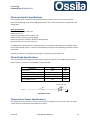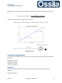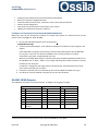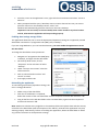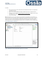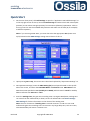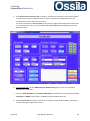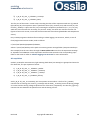
1
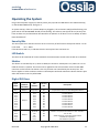
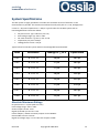
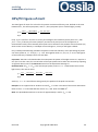
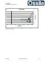
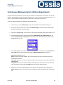
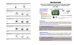
Ossila Smart PV and OLED Measurement System User Manual Ossila Ltd Copyright © 2009 - 2015 enabling innovative electronics CONTENTS OVERVIEW ....................................................................................................................................................... 4 SAFETY ............................................................................................................................................................. 5 EC DECLARATION OF CONFORMITY ................................................................................................................. 6 HARDWARE SETUP .......................................................................................................................................... 8 BOARD LAYOUTS ..................................................................................................................................................... 8 INTERCHANGEABLE BOARD CONNECTION .................................................................................................................... 10 OPERATING THE SYSTEM ............................................................................................................................... 11 SECURITY BITS ...................................................................................................................................................... 11 LED SWITCH ........................................................................................................................................................ 11 SHUTTER ............................................................................................................................................................. 11 DIGITAL DIO LINES ................................................................................................................................................ 11 CONTROLLING THE MULTIPLEXER ............................................................................................................................. 12 SYSTEM SPECIFICATIONS ............................................................................................................................... 13 ABSOLUTE MAXIMUM RATINGS ............................................................................................................................... 13 ELECTRONIC SWITCH SPECIFICATIONS ........................................................................................................................ 14 PHOTO DIODE SPECIFICATIONS ................................................................................................................................ 14 TEMPERATURE SENSOR SPECIFICATIONS .................................................................................................................... 14 COOLING FAN SPECIFICATIONS ................................................................................................................................. 15 HEATSINK ............................................................................................................................................................ 15 PHYSICAL CHARACTERISTICS .................................................................................................................................... 16 SOFTWARE DRIVER ........................................................................................................................................ 17 © MAX (MEASUREMENT AND AUTOMATION EXPLORER) .............................................................................................. 17 NI 6501 OEM OUTPUTS ....................................................................................................................................... 18 CODE EXAMPLE ..................................................................................................................................................... 19 EASY JV SWEEP SOFTWARE INSTALLATION ................................................................................................................. 19 HARDWARE CONFIGURATION ....................................................................................................................... 22 OPERATION & ACQUISITION MODE ............................................................................................................... 24 QUICK START ................................................................................................................................................. 25 DATA LOGGING TREE (FINITE MEASUREMENT MODE) .................................................................................................. 28 OPV/PV FIGURES OF MERIT ........................................................................................................................... 30 MAIN UI CONTROLS ....................................................................................................................................... 32 APPLICATION AND GLOBAL SETTINGS ............................................................................................................ 33 SYSTEM SETTINGS: OS CONTROL.............................................................................................................................. 33 SYSTEM SETTINGS: APPLICATION CONTROL ................................................................................................................ 33 SYSTEM SETTINGS: E-MAIL SETTINGS ........................................................................................................................ 33 ACQUISITION SETTINGS: SMU SETTINGS ................................................................................................................... 33 Ossila Ltd Copyright © 2009-2015 2 enabling innovative electronics ACQUISITION SETTINGS: SMU SETTINGS ................................................................................................................... 34 SENSOR SETTINGS: SMU SETTINGS .......................................................................................................................... 34 CONTINUOUS MEASUREMENT: LIFETIME EXPERIMENT ................................................................................. 35 LIFETIME LOGGING TREE STRUCTURE ........................................................................................................................ 36 LIFETIME START TIME............................................................................................................................................. 37 CONVERT BINARY INTO SPREADSHEET DATA ............................................................................................................... 38 MEASUREMENT AND ACCURACY ................................................................................................................... 40 TEMPERATURE AND SELF-CALIBRATION ..................................................................................................................... 40 CALCULATION OF THE MEASUREMENT ACCURACY ....................................................................................................... 40 TEMPERATURE EFFECTS ON SMU ACCURACY ............................................................................................................. 42 TROUBLESHOOTING....................................................................................................................................... 43 GUIDE TO THE READER: SYMBOLS, ACRONYMS, COMMON DEFINITIONS ...................................................... 46 WARRANTY INFORMATION AND CONTACT DETAILS ...................................................................................... 47 APPENDIX I .................................................................................................................................................... 48 Ossila Ltd Copyright © 2009-2015 3 enabling innovative electronics Overview The versatile Ossila USB test board allows automatic testing and measurement of multi-pixel OLEDs and PVs substrates to help make research and development faster, easier and cost-efficient. It comprises a main board (multiplexor) and one or more interchangeable substrate boards. The main board allows computer controlled multiplexing of eight individual signal lines. With each line connected to a specific pixel connector on the interchangeable board, a variety of substrate geometries can be easily characterised by simply connecting the appropriate test board to the Ossila multiplexor. The standard Ossila boards are also fitted with a reference thermometer and photodiode to allow automatic tracking of the environmental conditions during measurement. Computer control of the switching is provided by a National Instruments USB interface card to make programming easy in a variety of languages such as LabVIEW and MATLAB. Additional features include a cooling fan to keep substrate temperatures stable under high illumination, a TTL control for external systems (such as the shutter of solar simulators), and finally the possibility of connecting an external photodiode for OLED photocurrent characterisation. All of these features can be controlled automatically by the multiplexor. The versatility of the system makes it ideal for a wide variety of experiments including currentvoltage (JV) and current-voltagelight (JVL) sweeps, external quantum efficiency measurements and lifetime testing. Features: Can be used with interchangeable boads to allow use with a variety of substrate geometries. Extremely low pixel path resistance and noise/leakage current. Additional heatsink intergrated with the substrate holding bracket (optional). USB interface with easy integration to LabVIEW, MATLAB and others. Compatible with Linux, Mac OS, Pocket PC and Windows. On board temperature sensor. On board reference photo-diode (optimised for visible response). Shutter control for external instruments. On board cooling fan to keep substrate temperatures constant. Optical window for experiments where optical access is required from both sides. M4, M6 and 1/4" mounting holes to make mounting on a variety of optical benches and other equipment quick and simple. Please note that LabVIEW® is a trademark of National Instruments and MATLAB® is a trademark of The Mathworks inc. Ossila Ltd Copyright © 2009-2015 4 enabling innovative electronics Safety The Ossila USB test board is designed for low-voltage low-current applications and should not be used with high-voltage or high-current sources. It is also designed for use only with equipment featuring current and voltage compliance limiting to avoid either damaging the device under test or board electronics. Warning To avoid safety hazards obey the following: Only connect to low-voltage (<20 V) current (<100 mA continuous) power supplies. Do not leave devices with applied bias or current, unattended as a power failure may result in board damage or device damage and potentially hazardous situations. Caution To avoid damaging devices or equipment obey the following: Avoid electrostatic discharge (ESD) as this may damage the device. The Ossila OPV System uses MOSFETs which are static sensitive. To avoid damage use static discharge and prevention equipment where necessary. Only use the System for the purposes intended (described in this document) Do not expose the Board to any cleaning fluids or solvents. When a USB lead is first connected to the test board all pixels and outputs are switched to off, except the shutter and error LEDs. However, when USB connector is removed devices may be left in either an on or off state. As such, do not apply voltages or currents to the board without the USB power being applied. Ossila Ltd Copyright © 2009-2015 5 enabling innovative electronics EC Declaration of Conformity In line with directive 2004/108/EC of the European Parliament and of the Council and directive 2006/95/EC of the European Parliament and of the Council. -Manufacturer Name: Ossila Limited Manufacturer Address: Kroto Innovation Centre, North Campus, Broad Lane, Sheffield, S3 7HQ -Item: OFET testing rig for use with PXI system Model number: Software release: Easy JV Sweep -Specifications of product under harmonised standards: 2004/108/EC EN 61326-1:2006 Electrical equipment for measurement, control and laboratory use – EMC requirements – Part 1: General requirements IEC 61326-1:2005 EN 61326-2-1:2006 Electrical equipment for measurement, control and laboratory use – EMC requirements – Part 2-1: Particular requirements – Test configurations, operational conditions and performance criteria for sensitive test and measurement equipment for EMC unprotected applications IEC 61326-2-1:2005 2006/95/EC EN 61010-1:2010 Safety requirements for electrical equipment for measurement, control, and laboratory use - Part 1: General requirements IEC 61010-1:2010 EN 61010-2-030:2010 Safety requirements for electrical equipment for measurement, control, and laboratory use - Part 2-030: Particular requirements for testing and measuring circuits IEC 61010-2030:2010 Ossila Ltd Copyright © 2009-2015 6 enabling innovative electronics EN 61140:2002 Protection against electric shock - Common aspects for installation and equipment IEC 61140:2001 EN 61187:1994 Electrical and electronic measuring equipment - Documentation IEC 61187:1993 (Modified) EN 61010-2-081:2002 Safety requirements for electrical equipment for measurement, control and laboratory use - Part 2-081: Particular requirements for automatic and semi-automatic laboratory equipment for analysis and other purposes IEC 61010-2-081:2001 Declaration: I hereby declare that the equipment named above has been designed to comply with the relevant sections of the above referenced specifications. The unit complies with all applicable Essential Requirements of the Directives. -Signed: Name: Dr James Kingsley Date: Ossila Ltd Copyright © 2009-2015 7 enabling innovative electronics Hardware Setup Board Layouts Figure 1. Main board layout Figure 2. Interchangeable board layout Ossila Ltd Copyright © 2009-2015 8 enabling innovative electronics Reference number 1 Type Shutter BNC connector Description This connector can be used to control the shutter of a solar simulator. It is intended to be used with the Newport Oriel class A solar simulator or similar. Shutter is ON when P2.1 is pulled low. The shutter LED indicates when the shutter is OFF. Output (or input) connector for the DUT as well as the temperature sensor and photo diode with programmabable switching . Linked directly to the 2 way EXTERNAL header connector (6). It can be used for further expansion of the test board. Type B USB connector that allows for connecting a type A-B USB cable between a PC and the NI 6501 OEM board to control the multiplexer. National Instuments NI 6501 OEM Board. Can be used to attach an external photodiode. The Ext LED indicates when this connector active (ON). 2 Output BNC connector 3 External BNC connector 4 USB connector 5 6 NI 6501 External Connector 7 Photo diode 8 9 Power LED Error Indicator 10 11 POGO connectors Tmperature Sensor 12 Cooling fan 13 DC power jack 14 Used to connect to the incherchangeable boards. 15 16 Interchangeable Connectors LED switch Short LED Indicator 17 M3 Screws To stabilize the interchageable board and ensure correct connection. Ossila Ltd Photo diode with a peak sensitivity at 550nm. Note: The photodiode is foward biased. The PD LED indicates it is ON. Flashing LED to indicate 12 V power is connected. Switches on when the security bits have not been set. To set the security bit set P2.6 Low and P2.7 High POGO connectors to make contact with the substrate. A temperature sensor that outputs a current directly proportional to the temperature in Kelvin allowing easy measurement and calibration. The Temp Sens LED indicates it is ON. Cooling fan to ensure a stable substrate temperature. The Fan LED indicates it is ON. Used to power the cooling fan and the main board. Used to turn all the LEDs OFF. Indicates the short is ON. Can be used to short any of the pixels. Copyright © 2009-2015 9 enabling innovative electronics Interchangeable board connection Care must be taken when connecting the interchangeable board to the main board to ensure the headers from the detacheable board are inserted correctly into the main boad connectors or sockets (14), see figure 1. If the header pins are inserted into the wrong sockets the board will malfunction. To secure the interchangeable board in place there are four M3 screws (17), see figure 2 and figure 3, which also ensure the header pins are correctly aligned with the sockets. Also note the interchangeable board has a marking "TOP" to show orientation. Figure 1. Connecting the Interchangeable board to the main board. Ossila Ltd Copyright © 2009-2015 10 enabling innovative electronics Operating the System Plug in the 12V power supply into the DC power jack (13) and the USB cable to the USB B socket (4) on the NI 6501 OEM board, see figure 2. At system startup, if the 12 V power adapter is plugged in, the red Power LED (8) will be flashing. The green LED on the NI 6501OEM should also be flashing. The red Error LED (9) will be on (security bits have not been set) and the Shutter Off LED will be on (Shutter is off when P2.1 is set HIGH). All other LEDs should be off. Security Bits The security bits P2.7 and P2.6 must be set to control any of the functions except the shutter. To set: P2.6 -LOW P2.7 - HIGH If the Red Error LED is on, it indicates that the security bits have not been set. LED Switch The LEDs can be switched off via the LED SW if the measurement needs to be carried out in the dark. Shutter The shutter is controlled by P2.1, when set HIGH, the shutter is closed (LED is on). When P2.1 is set LOW the shutter is opened. The control can be applied to the solar simulator via the shutter BNC connector on the board. The shutter is the only function not controlled by the security bits. This fuction applies to solar simulators similar to the Newport Oriel Solar Simulators whose shutters open when the shutter control is pulled LOW. Digital DIO lines Signal Name Direction (software selectable) LED Indicator Security Bits Description P0.0 P0.7 Output PD Temp Sens Yes Yes Photo diode on Interchangeable board Temperature sensor on interchangeable board Output Px1 Px2 Px3 Px4 Px5 Px6 Px7 Px8 Yes Yes Yes Yes Yes Yes Yes Yes To select Pixel 1. To select Pixel 2. To select Pixel 3. To select Pixel 4. To select Pixel 5. To select Pixel 6. To select Pixel 7. To select Pixel 8. Output Short Shutt off Fan Ext Error Error Yes No Yes Yes Short, To short selected Pixels to Ground Shutter. To open/close shutter on solar simulator Turn on fan Allows external connection to Ext header Set LOW for operation Set HIGH for operation P1.0 P1.1 P1.2 P1.3 P1.4 P1.5 P1.6 P1.7 P2.0 P2.1 P2.2 P2.3 P2.6 P2.7 Ossila Ltd Copyright © 2009-2015 11 enabling innovative electronics Controlling the Multiplexer The multiplexer is controlled by the NI 6501 board. At the NI 6501 board startup and reset, the hardware sets all DIO (digital I/O) lines to high-impedance inputs. As each line has a weak pull-up resistor of 4.7 kOhm connected to it, all pins are set to HIGH. The default output configuration of the port pins is open-drain. This configuration allows the digital output signal to swing to 5V. Each port pin can be programmed as a digital input or output. To operate the system, the DIO lines should be programmed as digital outputs. NI 6501 Board Digital Logic Levels Level Input Input low voltage Input high voltage Input leakage current Output Output low voltage Open collector (open-drain) or active drive (push pull) IOL = 2 mA IOL = 8.5 mA Output high voltage Active drive (push-pull1) IOH = –2 mA IOH = –8.5 mA Open collector (open-drain), IOH = –0.4 mA, nominal Open collector (open-drain), IOH = –7.5 mA, with external pull-up resistor Min Max Units –0.3 2.0 — 0.8 5.8 50.0 V V µA — — 0.4 0.8 V V 2.8 2.0 2.0 2.0 3.6 3.5 5.0 — V V V V 1 The total current sourced by all DO lines simultaneously should not exceed 65 mA. Ossila Ltd Copyright © 2009-2015 12 enabling innovative electronics System Specifications The OPV system is highly specified to introduce the minimum amount of distortion in the measurement as possible. The resistance introduced in each pixel path is ˂ 0.2 Ω, leakage/noise current is ˂ 30 pA and capacitance is ˂ 350 pF. Typical values for the OPV system with an interchangable board are shown below. DC pixel current: typ 0- 100 mA ( max 1 A) Pixel voltage range: typ -20V to +20V On-state resistance: typ 0.1 Ω, max <0.2 Ω Capacitance per pixel < 350 pF Leakage/noise current: < 30 pA Typical values for the OPV system with an interchangeable board attached: Lines Resistance Leakage at 10 V Capacitance Px 1 R = 0.1 Ω 18 pA 283 pF Px 2 R = 0.1 Ω 17 pA 284 pF Px 3 R = 0.1 Ω 17 pA 269 pF Px 4 R = 0.1 Ω 18 pA 256 pF Px 5 R = 0.1 Ω 19 pA 304 pF Px 6 R = 0.1 Ω 17 pA 294 pf Px 7 R = 0.1 Ω 16 pA 263 pF Px 8 R = 0.1 Ω 15 pA 241 pF Absolute Maximum Ratings DC pixel current: 1 A ( One pixel at a time) Pixel voltage range: -20V to +20V Shutter output current: 2 mA Digital I/O header pin current: 2 mA Power Adapter (+12VDC connector) Output current: 830mA External BNC current: 0.5 A DC Digital I/O voltage range: -0.5 to 5.8 V with respect to GND Ossila Ltd Copyright © 2009-2015 13 enabling innovative electronics Electronic Switch Specifications Each indvidual pixel as well as the photodiode and temperature sensor can be turned on/off electronically through a network of high performance relays. Each pixel/device is connected to the output BNC . Relay specifications Max switching voltage: 220 V DC Rated current: 2A Capacitance between open contacts: 1pF Minimum Relay switching voltage 100µV Relay initial contact resistance: 50 mΩ at 10 mA/20 mV Relay operate time: typ 3 ms, max 5 ms The multiplexer comprises eleven single channels. It is capable of switching one or multiple inputs to the common BNC output. A switch is turned ON by setting the corresponding control bit into the HIGH state. Similarly, the switch is turned OFF by setting the control bit into the LOW state. Photo Diode Specifications The on board GaP photo diode has been chosen to give a response in the visible spectrum with a peak sensitivity at 550 nm; the photodide is foward biased. Parameter Active area Peak sensitivity, typ. Sensitivity spectral range Acceptance angle half angle Reverse dark current Type 9.8 550 400-700 60 100 Unit mm² nm nm deg. nm Photo diode (PD) P0.0 Output Equivalent circuit Temperature Sensor Specifications The temperature sensor acts as a current source with an absolute accuracy of ±3°C with an output current directly proportional to temperature in Kelvin. Ossila Ltd Copyright © 2009-2015 14 enabling innovative electronics The temperature can be calculated according to the following formula, note the output current is in µA: Therefore, the temperature in degree Celcius is equal to: Temperature sensor (TEMP) P0.7 Output Equivalent circuit Cooling fan specifications The cooling fan is provided to keep devices at a constant temperature when illuminated under solar simulators . Rated voltage: 12VDC Rated power: 0.48W Air delivery: 4.6 CFM Power current: 40 mA Heatsink There is an optional heatink which can be attached beneath the bracket to further cool the substrate. Material: aluminium Ossila Ltd Copyright © 2009-2015 15 enabling innovative electronics Physical Characteristics Dimensions: 190 mm (L) x 138 mm (W) x 40 mm (H) I/O connectors: o 1 x USB series B receptacle (cable included) o 3 x BNC receptacle o 1 x 2 way header pins to allow attachement of external photodiode Weight: 245 g Insulating M6 bolts & washers, M3 screws. USB A/B cable is included. Cooling fan and. +12 V adapter included. Ossila Ltd Copyright © 2009-2015 16 enabling innovative electronics Software Driver The Ossila OPV System is controlled by a National Instruments USB 6501 OEM system to allow easy interface with a range of languages and is compatible with Linux, Mac OS, Pocket PC and Windows. Languages that can be used include: LabVIEW MATLAB (Data Acquisition toolbox required) ANSI C LabWindows/CVI Measurement Studio Visual Basic Visual Studio Visual Studio .NET In order for the Ossila OPV System to be recognised by your computer, please ensure that the National Instruments DAQmx driver version 14.1 or above is installed on your system. Many computers running LabVIEW with other national instruments hardware will already have DAQmx drivers installed and should recognise the board instantly. To check if DAQmx is installed on a PC navigate to Start Menu -> All Programs -> National Instruments and look for NI-DAQ. If DAQmx is not installed on your system, please download and install it from the National Instruments Website (www.ni.com) where it is available free of charge (registration required). MAX© (Measurement and Automation Explorer1) Legal Notice: This section is neither a comprehensive nor a partial User’s guide to Measurement and Automation Explorer or any other National Instruments (hereafter NI) products. The scope of this section is to provide the Users with the information necessary to install, test and maintain the accuracy level of the Ossila measurement system. Accordingly, this section is exclusively intended for Ossila OPV system users and any other use is explicitly forbidden. Please refer to National Instruments Measurement and Automation Explorer Help for comprehensive documentation and User’s guide. MAX is an NI product covered by one or more of the following Patents: U.S. Patent No(s) 6,690,390; 7,130,760; 7,134,109; 7,152,116. Introduction MAX (Measurement and Automation Explorer) is the National Instruments application that provides direct access to NI hardware. According to NI specifications2, MAX can be used to 1 MAX, Measurement and Automation Explorer, ©1999-20013 National Instruments. All right reserved Ossila Ltd Copyright © 2009-2015 17 enabling innovative electronics Configure your National Instruments hardware and software Back up or replicate configuration data Create and edit channels, tasks, interfaces, scales, and virtual instruments Execute system diagnostics View devices and instruments connected to your system Update your National Instruments software Configure and Test National Instrument NI 6501B OEM Board Make sure that all the connections between the Ossila OPV System are well-connected, all the power cords are plugged in. Open NI MAX; 1. On the left side MAX subpanel, click on My System. NI USB-6501 Settings 2. Click on Device and Interface: a list of devices installed or simulated on the computer will appear. If the USB cable is properly connected to both PC and the OPV System, the NI USB-6501 icon is green. The icon of a device installed but not currently present or properly connected is grey with a superimposed red cross; When first installed, MAX assigns a standard alias name to MAX-compatible hardware. For NI USB-6501, this is “Devn”, where n is a integer indicating the number of device currently installed on the computer. If required, o change the alias right-click on the alias name, select Rename on the dropdown menu and input the new alias. 3. Familiarise with the tool bar commands on the central subpanel of MAX, see Fig. 6, 4. Use Reset to reset the hardware and Self-Test to test the hardware. NI 6501 OEM Outputs The USB 6501 controller has 24 DIO channels arranged in three groups of eight Signal Port 0 P0.0 Photodiode P0.1 Unused P0.2 Unused P0.3 Unused P0.4 Unused P0.5 Unused P0.6 Unused P0.7 Temperature sensor 2 Signal Port 1 P1.0 Pixel 1 P1.1 Pixel 2 P1.2 Pixel 3 P1.3 Pixel 4 P1.4 Pixel 5 P1.5 Pixel 6 P1.6 Pixel 7 P1.7 Pixel 8 Signal Port 2 P2.0 Short P2.1 Shutter P2.2 Fan P2.3 External P2.4 Unused P2.5 Unused P2.6 Safety bit Low P2.7 Safety bit High Measurement and Automation Explorer Help, Version 370694R-01, June 2013. Ossila Ltd Copyright © 2009-2015 18 enabling innovative electronics Code example Code examples written in LabVIEW and MATLAB can be found on the product webpage at www.Ossila.com MATLAB code example LabVIEW code example Ossila Ltd Copyright © 2009-2015 19 enabling innovative electronics Easy JV Sweep Software Installation To install the application: Insert the installation CD in the target computer, Copy the .rar folder containing the application to the target computer Uncompress the folder and browse to the executable file called setup contained in the Volume folder Note: Do not move, modify or delete any file or folder contained in the Volume folder prior completion of the installation. Run the executable and follow the instructions to install the application in C:\Programme Files (86X)\Easy JV Sweep\ The drivers shipped with the application will be automatically installed in the folder C:\Programme Files (86X)\National\ Reboot the target computer to complete the installation. You can now remove the both .rar and Volume folders. Important! Do not install this application on a target computer running Labview. If the target PC is already running Labview, you should run the executable instead. Contact Ossila at [email protected] for further information on installing and using the executable on a target computer already running Labview. Required drivers 1) 2) 3) 4) 5) 6) 7) 8) LabVIEW® Run-Time Engine 2014 or later version. NI-488.2 Application Development Support 14.0 or later version3 NI-DCPower Development Support (only for NI PXI-4132 SMU)4 NI-DAQmx Runtime with configuration support NI System Configuration Runtime NI-Measurement & Automation Explorer 14 NI-VISA Runtime Engine 14.0 or later version NI-VISA Configuration Support 14.0 or later version The drivers are shipped with the application and are automatically installed by the NI Installer on the target PC. Post installation After installation, a shortcut should appear on the User Desktop. If the shortcut fails to show: Navigate to the application executable in C:\Programme Files (86X)\Easy JV Sweep\ 3 For this drivers, install the full development support to allow full configuration control through MAX. For this drivers, install the full development support to allow full configuration control through MAX and the “soft panel” (NI native User Interface) functionalities. 4 Ossila Ltd Copyright © 2009-2015 20 enabling innovative electronics Place the cursor on the application’s icon, right click the mouse button and select “Create a Shortcut” When prompted with the query “Windows cannot create a shortcut here. Do you want to place the shortcut on the desktop instead”, select “Yes”. Windows will automatically place the shortcut on the User’s desktop. Important! The icon itself (i.e. the executable) must not be moved to any other location on disk, otherwise the application will stop working properly. Enabling data settings storage folder The application allows the user to save the Experiment/Acquisition settings in an appositely created data folder contained in C:\Programme Files (86X)\ Easy JV Sweep \. If you are using Windows 7, 8, 8.1 or later distributions, you must enable the application to write the data folder. To change the data folder access permission: Navigate to C:\Programme Files (86X)\Easy JV Sweep\, and right click the data folder On the drop-down menu, click on “Properties” and on tab menu of select “Security”. Under “Group or user names” select the relevant PC user Click on edit and make sure that “Full control” is ticked Press apply and then OK Reinstalling the application To avoid losing experiment/acquisition settings, the User is strongly advised to: Make a copy of the data folder After the re-installation is completed, delete the content of the new data folder with the exception of the file with extension .ddl Copy all the files in the old data folder to the new data folder, again with the exception of the file with extension .ddl. Note: Make sure to delete every single file in the new data folder and replace them with the entirety of the file in the data folder (with the exception of the .ddl file), otherwise the application may stop working properly. Alternatively, before re-installing the application, delete the data folder to delete any previous reference to old experiment settings. Ossila Ltd Copyright © 2009-2015 21 enabling innovative electronics Hardware Configuration In order for the application to communicate and control the acquisition hardware (SMU), alias names must be assigned to the SMU and peripheral units through NI MAX (Measurement& Automation Explorer)5. NI (National Instruments) hardware will appear on MAX with their factory alias name. For example, the multiplexer unit hosts a NI USB card interface and will appear on MAX as Dev1. If more than one NI USB card has been connected to the target computer, MAX will automatically assign a different, sequential number, to the multiplexor. Important: If the SMU of choice is the 4132 NI-PXI, the computer needs to be rebooted after the PXI chassis is turned on in order to link the PXI to the target PC. If the reboot is not executed, neither MAX, nor SuperFACT will be able to communicate with the PXI hardware. To configure multiplexor and SMU, take the following actions, see figure 12. With the system fully set-up (i.e. with every hardware units properly connected, see Hardware Setup), open NI MAX and click on My System and the on Devices and Interfaces. Multiplexor (through NI USB Card) Search for Dev1 (the identification number may be different, see explanation above) and right click on this entry to show the drop-down menu options. Select Rename and rename Dev1 as “SwitchControl20” (this name is case sensitive). For Keithley SMU In Devices and Interfaces search for the GBIP device and, with the mouse, left-click to expand the list of devices connected to the target PC through the GBIP interface. If the list is empty, on the control bar located on the top side of MAX right panel, click on Scan for instrument. Providing Keithley 26XX SMU is properly connected and switched on, MAX will identify this SMU with its VISA resource name (GPIB0::NUMBER::INSTR). Under Devices and Interfaces, click on the VISA NAME to show the Settings panel for this VISA instrument on the right side panel of MAX On the Settings panel, go to Name and replace the default alias name with KeithleyO (case sensitive) Save the new settings using the Save button on the control bar of the Settings panel. 5 If MAX is not yet installed, please download and install it. MAX is freely available at www.ni.com; registration to NI website may be required to download NI applications and drivers. Ossila Ltd Copyright © 2009-2015 22 enabling innovative electronics For NI-PXI On the left side panel, click on the arrow next to NI PXIe-1071 “Chassis 1” to expand the associated tree menu. Right click on NI PXIe-83060 and change the default alias name to “Remote Control”. Navigate to the two SMU units (NI PXI 4132) and rename them as “SMUA” (unit in slot 2) and “SMUB” (unit in slot 3). These alias names are case sensitive. Save the new settings Note: MAX allows the user to reset, self-test and self-calibrate (if applicable) any NI hardware. For VISA instruments (such as Keithley), MAX is shipped with an equivalent VISA Test Panels. In addition, it gives direct access to these instruments via text-based command strings. These functionalities usually require that the corresponding full hardware drivers are installed on the host computer (see Easy JV Sweep Software Installation) Figure 2. MAX (Measurement & Automation Explorer) user interface. Ossila Ltd Copyright © 2009-2015 23 enabling innovative electronics Operation & Acquisition Mode Easy JV Sweep can automatically acquire JV/JVL curves of a multi-device substrate by switching over the different channels of a multiplexor. Since each multiplexor channel is associated (connected) to a different device on the substrates through the cathode and anode POGOs mounted on the interchangeable board, see Board Layouts, the DUTs can be automatically characterised by selectively turning ON/OFF these channels. Refer to the Sec. Quick Start for more details on how to set up an automatic acquisition. Important: The Ossila multiplexor “USB1” must be connected to the host PC via a USB cable, otherwise error code 5040 will be returned and no measurement can be carried out. Easy JV Sweep supports two main acquisition modes: Finite Measurement and Continuous Measurement. Finite Measurement: one single measurement is carried out per substrate/device (Standard JV/JVL characterisation). The JV(or JV/JL) curves and the figures of merit of the DUTs are then saved in a set of CSV files, one per each acquisition session and data type. For example, the JV curves will be all saved on a single file so as to facilitate data handling and statistical analysis. Continuous Measurement: multiple measurement cycles of the selected devices executed consecutively or intermittently for a protracted period of time. Continuous measurement is designed for gathering lifetime data on the device performance over a user-defined period of time, whose duration can be, at the most, infinite. The diode figures of merit are stored as time series on a single .csv file per device. The same for the JV/JVL curves. Ossila Ltd Copyright © 2009-2015 24 enabling innovative electronics Quick Start 1. On the main front panel, click Add Settings to open the “Application and Global Settings” UI. In the top-right corner of this UI, locate LT: Data Storage and select which disk volume (disk partition) to use as data storage repository for Continuous (Lifetime) experiments. Click on the ring control to see the available disk partitions and select one of them (D, for example) as lifetime repository. Note: If you are using NI-PXI 4132, you must also select the appropriate PLC (Power Line Cycle) located on the SMU Settings setting control cluster of this UI. 2. Upon pressing Go To Exp, the current UI is closed and replaced by “Experiment Settings” UI. 3. On Experiment Settings, locate the SMU Setting (JV) control panel located on the top left side of the screen, and enter the Gate SMU Name and Channel name. SMU Name is the SMU alias name specified in MAX (KeithleyO or SMUB), while channel is smub for Keithley SMU or 0 for PXI. Set Auto Zero = Once 4. Enter the Settling Time, the gate source settling time. For Organic OPV/OLED, settling time can varies from few milliseconds (or lower) to tens of milliseconds. See Sensor Settings: SMU Settings for further information on the choice of the settling time. Note: The unit of measure of Settling Time is seconds. Enter 0.1 or 100 m to set a 100 milliseconds gate source settling time. Do not enter very large delay time, such as 10 secs, otherwise Keithley will return a timeout error. Ossila Ltd Copyright © 2009-2015 25 enabling innovative electronics 5. Enter Current Limit. Current Limit, in Ampere, specifies the maximum current that the SMU is expecting to measure during the current session. Therefore, the SMU determines the measurement current range from this value. For more information on Current Limit, measurement range and the implication of the latter on resolution and accuracy, refer to Calculation of the Measurement Accuracy and to the SMU Data Sheet. 6. For OLED/LED only. On the SMU Setting (JL-Photocurrent) panel, press JVL to enabled photocurrent acquisition. 7. Enter the Gate SMU Name and Channel. SMU Name is the SMU alias name specified in MAX (KeithleyO or SMUA), while channel is smua for Keithley SMU or 0 for PXI. 8. Enter Current Limit in Ampere to specify the maximum current that the SMU is expected to measure during the acquisition session. Ossila Ltd Copyright © 2009-2015 26 enabling innovative electronics 9. Enter Settling Time. The JVL Settling Time starts on completion of JV Settling Time (see above) and is therefore used to add a delay between the output current and photocurrent acquisition. Unless a delay between the two current measurement is required, set JVL Settling Time = 0. Set Auto Zero = Once. 10. On the Sweep Setting panel, define the sweep parameters by imputing (in Volts) Voltage Start, Voltage End and Delta V. The data points In(Vn) are given by Vn = VStart +nΔV, Eq. 1 with Eq. 2 In addition to the data points specified in Eq 1, Easy JV Sweeps always acquires a data point at Vn = 0 and Vn = VEnd. Important: No matter what the DUT architecture is (see below), Voltage Start must be negative and Voltage End positive. 11. Dev Area specifies the pixel area (in cm2) or the area of the ‘windows’ of a measurement aperture mask. 12. Select the Device Type (Direct or Inverted). Device Type is the architecture of the Cells: Direct (or standard): The electrons are supplied by a low work function metal, such as calcium, while the anode is a high work function material such as ITO. Inverted: High work-function metal (such as ITO) in combination with electron transport layer (such as PFN) can be used as cathode, while the anode is provided by a second high work function material (Al, Ag etc). 13. Short? is used to set the pixel status between two consecutive measurements in continuous acquisition mode. If Short? is set to Short, the cathode and anode of each pixel on the substrates are shorted together, i.e. the measurement circuit is ‘closed’. Conversely, If Short? is set to Open, the cathode and the anode are floating, i.e. they are not connected together. Ossila Ltd Copyright © 2009-2015 27 enabling innovative electronics 14. On Experiment Settings fill in the entries User Name, Exp. Name and File Name. These inputs are used by JV Easy Sweep to create a User’s data logging directory tree, refer to the section Data Logging for more information. 15. Use the browse button of Data Folder Path to enter the path to the directory to be used as repository folder, i.e. the folder containing the data logging directory tree (see above). 16. Select the pixels to measure by pressing the corresponding button (1 for Pixel 1, 2 for pixel 2, and so forth). 17. (Optional) Use Notes input field to save any relevant annotations. 18. Press the Commit button to save the experiment settings 19. To start the experiment, press Start on the main UI, enter the file name and press OK. The acquisition will start. Note: A committed experiment is loaded into memory, but not permanently saved, and therefore it will be overwritten every time a new experiment is loaded into memory or the application is closed. Save Experiment Settings If the experiment settings are intended to be used for successive acquisitions, these settings can be permanently saved by making use of the Save button on the Experiment Settings UI. Important: If you save an experiment, you still need d to commit it in order to execute the experiment, refer to the section Main UI Controls below detailed instruction on how to commit an experiment. Important: Upon pressing Start on the main UI, Easy JV will execute the experiment settings of the last committed experiment. If you choose to save an experiment by pressing Save, Easy JV will not update the settings loaded into memory. Consequently, to use a newly saved experiment, you always need to commit it first. Refer to the Main UI Control below for details instruction on how to commit a saved experiment. Data logging Tree (Finite Measurement Mode) JV acquisition For each acquisition session, the data and OPV/PV figures of merit are saved in a set of three files, namely 1) Y_M_D -hh_mm_ss_FileName_Header Ossila Ltd Copyright © 2009-2015 28 enabling innovative electronics 2) Y_M_D -hh_mm_ss_FileName_JV Sweep 3) Y_M_D -hh_mm_ss_FileName_Data, The first part of the name is a time stamp recording the date of the acquisition with Year (Y), Month (M) and Day (D). The acquisition time is specified as hours (hh), minutes (mm) and seconds (ss). The first file (_Header) is a plain text file (.txt) containing the acquisition parameters (VStart, VEnd, ΔV, etc), while the second records the JV sweep, one per DUT. Finally, the third one contains the solar cell figures of merit such as PCE, FF etc and the environmental sensor data (photodiode and temperature sensor) Easy JV Sweep organises the data file according to a data logging tree structure, which, in case of finite/single measurement mode, reads as follows C:\Users\Pier\Desktop\ExpName\FileName, where C:\Users\Pier\Desktop is the path to an existing master storage folder (computer Desktop in this example) that the user select through the Data Folder Path control on the Experiment Settings UI. ExpName and FileName are the experiment and file name entered in the corresponding input fields on the same UI. Refer to Lifetime Logging Tree Structure for more information. JVL acquisition Similarly to OPV/PV measurements, light emitting diode data (JVL sweeps) are grouped and stored in four data files, one per acquisition session: 1) 2) 3) 4) Y_M_D -hh_mm_ss _ FileName _Header Y_M_D -hh_mm_ss _ FileName _JV Sweep Y_M_D -hh_mm_ss _ FileName _JL Sweep Y_M_D -hh_mm_ss _FileName_Efficacy with Y_M_D -hh_mm_ss timestamp, see JV acquisition section above. The first file (_Header) contains the JVL settings; the second (_JV Sweep) and the third (_JL Sweep) stores the driving voltage Vs current and the driving voltage Vs photocurrent of the DUTs, respectively. The last file (_Efficacy) contains the ratio between the photocurrent and the driving current. Ossila Ltd Copyright © 2009-2015 29 enabling innovative electronics OPV/PV Figures of merit The main figure of merit of a solar cell is the power conversion efficiency, PCE, defined as the ratio between , the cell output power, and , the input power (sun or artificial light), namely , Eq. 3 In Eq. 3, and are the J-V current and voltage at the maximum power point , with density of current (mA/cm²) and A area of pixel (or area of the aperture of measurement mask). The maximum power point can be written as the product of the Fill Factor (FF), Short Circuit current density JSC and Open Circuit voltage VOC, see Eq. 3 and figure 5 below. Easy JV Sweep automatically calculates the power conversion efficiency as the percentage of power out versus power in, i.e. . PCE together with JMPP, VMPP, FF, JSC VOC are the figures of merit that Easy JV Sweep returns for each DUT. Important: The PCE is calculated under the assumption the power of the light source PIn is equal to 1 Sun. If PIn less than 1 Sun, the actual value of the input power can be taken into account by inputting an effective device area in the Dev Area control on the Experiment Settings UI. Demonstration: If is the actual input power, with 0 attenuation factor of the light source, then we can write Eq. 4 with is the effective area given by the product of the pixel area A and . Example: Let us suppose that A =0.0212 cm2 and Sun. The value of the source attenuation factor is the and the effective area is =0.9 ∙0212 =0.01908 cm2. Note: The photodiode measures a current of approximately 1 mA for Ossila Ltd Copyright © 2009-2015 = 1 Sun. 30 enabling innovative electronics JV Sweep 25 20 15 5 0 -5 J mA/cm2 10 -10 -15 -20 -25 -200 0 200 400 600 800 1000 Voltage (V) Figure 3. JV Sweep with max power point (PMax), open circuit voltage (VOC) and short circuit (density) of current (JSC). Ossila Ltd Copyright © 2009-2015 31 enabling innovative electronics Main UI Controls Run starts an acquisition session by running the committed experiment in memory. Add Setting is used to enter a new experiment setting. Refer to the section Quick Start for a detailed explanation on how to specify a new experiment setting. Del Settings allows the user to delete an existing (saved) experiment setting. To delete an experiment: 1. Click on Del Settings. 2. On the List of Saved Experiment UI select the experiment to delete and press the Delete button. See Setting opens the current experiment setting. Tip: Use See Setting to modify an existing experiment or to save a new experiment that is similar to an existing one. Load Settings loads into memory and commits an existing experiment setting. To commit an experiment’s settings: 1. Click the Load Exp button on the main UI; the List of Saved Experiment UI will open. 2. On List of Saved Experiment UI, select the experiment that you want to commit and press the blue Commit button. The Application and Global Settings UI will open. Press the Go To Exp button to confirm the advanced setting. On the Experiment Settings UI, press Commit to commit the current experiment. This experiment is executed by pressing Start on the main UI. FAN switches the board fan ON and OFF. Control not available while an experiment is running. SHUTTER opens/closes the shutter. This control is not available while an experiment is running or for JVL (OLED/LED) acquisition. Note: Shutter send a TTL signal to the shutter. The ouput signal, however, is inverted, i.e. the ouput is LOW (≤ 2 V) when the SHUTTER is ON, and HIGH (2.6 V ≤ Shutter ≤ 5V) when the SHUTTER is OFF. HW RESET is used to reset the hardware (SMU and USB Card) and to refresh the display. STOP interrupts the running experimnet. If Easy JV Sweep is operating in Continuous Measurement Mode (lifetime), the experiment is stopped after the current substrtate cycle is completed, i.e. after all the DUTs are swept. Ossila Ltd Copyright © 2009-2015 32 enabling innovative electronics Application and Global Settings This UI controls the application and SMU settings. System Settings: OS Control Windows Reboot Time sets the PC reboot time– available in Continuous Measurement mode only. Reboot enables/disables the reboot functionality System Settings: Application Control AutoRun enables automatic acquisition functionality whereby a lifetime experiment is initiated whenever the application is started. Use this functionally together with reboot to automatically restart a lifetime acquisition or to initiate at a set date. Note: Easy JV Sweep not currently shipped with auto-start functionality; use Windows Time Scheduler with AutoRun set to ON to automatically start the application and initiate a life time acquisition at a predetermined time. Self-Calibration enables/disables SMU self-calibration routine at lifetime acquisition start. This feature is available for PXI SMU only. AUTORESET forces the application to execute a hard reset at when the application is started (Controls available with NI PXI only). System Settings: E-mail Settings It enables automatic e-mailing functionally whereby errors and failures messages are e-mailed to the e-mail address specified in Sender’s Email Address. Available in Lifetime mode only. Acquisition Settings: SMU Settings PLC (Power Line Cycle) specifies frequency of the electric power grid(50 or 60 Hz). Keithley 26XX series automatically detected the PLC of the power supply grid. Power Line Cycle is the oscillation frequency of the AC current supplied to the end-users through the electrical power grid. In the EU, Australia, part of Japan and several other countries, the PLC is 50 Hz with a voltage range of 220-240 V. In USA, Canada and Taiwan, part of Japan, etc the PLC is 60 Hz with a voltage range of 100-120 V. Ossila Ltd Copyright © 2009-2015 33 enabling innovative electronics Note: Providing the correct PLC is detected/set, SMU are usually equipped with built-in filter capable of rejecting the noise originated from the oscillatory behaviour of the power supply. This SMU capability is often referred to as PLC noise rejection. Sample to Avg specifies the number of current readings that the SMU requires to output a single measurement point. For example, if Sample to Avg is set to N, the SMU takes N independent measurements, which are then averaged so that a single (averaged) output is returned. Increasing N will increase accuracy at the cost of measurement speed. N=1 is usually adequate unless stringent accuracy requirements, or specific measurement needs, require larger data sample. Refer to the SMU user’s manual for the maximum number of sample to average supported by the SMU. Aperture Time sets the duration of a single current (or voltage) reading. Aperture Time is expressed in unit of PLC. The actual value of Aperture Time therefore depends on the PLC frequency, as detailed in the following table where Aperture Time is expressed in term of PLC units and seconds. PLC 8 4 2 1 1/2 1/4 1/8 1/16 1/32 1/64 Aperture Time PLC Input 60 Hz 8 133 ms 4 66.6 ms 2 33.3 ms 1 16.6 ms 0.5 8.33 ms 0.25 4.16 ms 0.125 133 ms 0.0625 1.04 ms 0.031250 520 µs 0.015625 260 µs 50 Hz 160 ms 80.0 ms 40.0 ms 20.0 ms 10.0 ms 5.00 ms 2.50 ms 1.25 ms 625 µs 312 µs As for sample to average, longer aperture time increases accuracy by slowing down the acquisition rate. Acquisition Settings: SMU Settings Data Storage Volume specifies the disk volume (partition) used as repository for the life data acquisition. To be used as repository volume, a disk partition must have at least 1 GB of free space. Important: You can use external disk partition as well (such as USB memory card, server’s volumes etc). If you use an external memory storage facility, make sure that the connection with the host computer is stable and reliable so as to avoid data acquisition failure due to the peripheral becoming disconnected and/or irresponsive. Sensor Settings: SMU Settings The panels in this section control the sensor on the board (photodiode and temperature session). The same as SMU Settings, it controls the SMU setting for sensor acquisition. Current Limit specifies the maxium current (in ampere) that the sensor is expected to ouput. Settling Time is the time that the SMU is forced to wait before taking a sensor reading. Ossila Ltd Copyright © 2009-2015 34 enabling innovative electronics Continuous Measurement: Lifetime Experiment Continuous mode acquisition is used to carry out lifetime characterisation of the DUTs. The JV (JVL) and the relevant figures of merit are saved as time series, i.e. as function of the elapse time Δt = ta-t0, with ta = time at which the measurement is taken and t0 experiment starting time. To set up a lifetime experiment, follow the instruction below. 1. On the main UI, press Add Settings to open the “Application and Global Settings” UI. 2. In the top-right corner of this UI, locate LT: Data Storage and select the disk volume (disk partition) to allocate for data storage. 3. Upon pressing Go To Exp, the current UI is closed and replaced by “Experiment Settings” UI. 4. On “Experiment Settings” fill the controls panels SMU Setting (JV), SMU Setting (JL-)- for OLED, Sweep Setting, and Experiment as detailed in the Quick Start section of this User’s Manual (points 3 to 17). 5. On the Life Time panel, enable continuous measurement mode by selecting Ad Infinitum or Time Limit option from the drop-down menu of Measurement Cycle ring control. Measurement Cycle options: Select. Continuous mode disabled, only one acquisition per DUT is executed during the measurement session. Time Limit. Continuous mode is enabled and the DUTs are swept up to the time specified in Life Time End. Ad Infinitum. Continuous mode is enabled. The experiment will continue to run unless the User terminates it by pressing the STOP button on the main User Interface. 6. Specify the interval (idle time) between two consecutive acquisition cycles through the Meas. Interval controls. The time interval is imputed as Hours (H), Minute (M), and Second (S). Ossila Ltd Copyright © 2009-2015 35 enabling innovative electronics 7. To turn ON/OFF the fan during JV sweep, set the Fan During Sweep control on the Application Control panel to ON/OFF. LT: Fan Idle Time turns ON/OFF the fan during the idle time between acquisition cycles. Note: If Fan During Sweep = OFF and LT: Fan Idle Time = ON and Meas. Interval is different from zero, the fan will be operating during the idle time only. 8. The shutter can be set to remain open during the idle time through the LT: Shutter Idle Time button. Note: For JVL acquisition setting, LT: Shutter Idle Time has no effect on the shutter TTL output, but it will force the external channel, see Board Layout, to remain open during idle time. 9. Hit the Save button to save the experiment settings. 10. To run the experiment, press Load Settings button on the main UI, and surf through the “Application and Global Settings” and “Experiment Settings” UI. 11. On “Experiment Settings” UI, hit the Commit button to commit the experiment. 12. On the main UI hit Run to initiate the acquisition. Important: You can stop and start a lifetime experiment through the STOP and Run command on the main UI. If you stop a lifetime experiment, this will remain committed even if the application is closed. The lifetime can therefore be restarted by hitting Run on the main UI. Conversely, if a different experiment is committed, the lifetime experiment must be reloaded in memory (see instructions 10 to 12 above). Lifetime Logging Tree Structure Lifetime data is organized and stored in the data storage volume according to the following logging tree structure: Volume:\LifeTime_Ossila_MB\SweepType\ExpName\FileName\DataFiles Ossila Ltd Copyright © 2009-2015 36 enabling innovative electronics Volume is the user selected disk partition (disk volume), see instruction 2 above. LifeTime_Ossila_MB is the master directory containing the entirety of the Lifetime data saved in Volume. LifeTime_Ossila_MB is automatically created whenever the user chooses a different data storage volume. SweepType directory is used to organise the PV/OPV and LED/OLED measurement in two separate groups. SweepType =JV or JVL depending if the DUT is a solar cell or light emitting diode, respectively. ExpName and FileName directories are the experiment and file name as specified on the “Experiment Settings” UI with the ExpName and FileName controls. DataFiles are the files containing the raw measurement and the DUTs figures of merit. Important: The data are saved in binary format and therefore are not directly human readable. Use Ossila Data Converter to convert the binary file into comma-separated values (.csv) files. CSV files can be opened by any spreadsheet application, including MS Excel©. See section Convert Binary Into Spreadsheet Data below for detailed instructions on how to quickly and easily convert binary into CSV files. Lifetime Start Time Lifetime data is saved as functions of the time elapsed from the beginning of the acquisition. It is therefore paramount that the user makes sure that Easy JV Sweep records the correct start time. Easy JV Sweep takes the time t0 at which the lifetime experiment was saved as starting time of the experiment. The elapse time (Δt) at ta is then calculated as Δt= ta- t0, with ta time at which the measurement a is taken6. It follows that the User must save the lifetime experiment settings just before starting new experiment settings. Important: If the same experiment setting is later on used for different substrates, the User must resave this experiment (or overwrite it) to make sure that the new starting time is correctly recorded. The User should also make sure that either the older data is removed from the data storage directory, or the new experiment/substrate is saved with a different data logging tree structure. In fact, if the new experiment shares Volume, SweepType, ExpName and FileName with the old one, the new data will be appended to the old substrates data files. 6 Here, a represents a specific DUT lifetime acquisition cycle. So a = 1 for the first acquisition, a = 2 for the second acquisition cycle and so on, so forth. The DUT figures of merit, PCE for example, are then saved as PCE(t1- t0 ), PCE(t2- t0 ), etc. For example, plotted as function of Δt, PCE(Δt) represents the time series (lifetime curves) of the solar cell efficiency. Ossila Ltd Copyright © 2009-2015 37 enabling innovative electronics If multiple substrates are employed for a lifetime experiment7, to avoid mixing the data from different substrates the user must define a unique Experiment Name for each substrate. Convert Binary Into Spreadsheet Data To convert the lifetime data from binary to comma-separated value files readable by any spreadsheet application such as MS Excel©, follows the step detailed below. 1) Open Easy JV Sweep data conversion 2) Use the Brower button of the Experiment path input to navigate to the folder containing the binary data file. For example, if the DataFiles are stored in Volume:\LifeTime_Ossila_MB\SweepType\ExpName\FileName\DataFiles, you need to navigate to the directory FileName, and select Current Folder in the bottom-right corner of the navigation windows, see below. 7 Lifetime measurement is usually carried out by continuously measuring the DUTs. However, limited resources, constrains on the use of the measurement infrastructure, minimisation of the cost, finite lifespan of solar simulator lamp etc, can make continuous lifetime acquisition unfeasible. However, for environmental degradation studies, periodical (daily) measurement can suffice. By exploiting the continuous measurement mode feature, the acquisition data can be automatically saved as time series instead of being recorded as separate files as it is the case for finite measurement. Ossila Ltd Copyright © 2009-2015 38 enabling innovative electronics 3) Using the browse button of the Target Path control, select the target directory, i.e. the directory where the CSV files are to be saved. 4) Press Save As Excel to convert and save the binary file in CSV files. 5) Hit Exit to exit the Data Converter Important: Target Path cannot be a sub-path of the Experiment path (i.e. you cannot save the CSV file in the directory containing the binary file), otherwise Data Converter will return an error. Ossila Ltd Copyright © 2009-2015 39 enabling innovative electronics Measurement and Accuracy The two PXI Source Measurement Units (SMUs) are capable of very accurate voltage and current measurements, see “SMU Specifications” section in the NI PXI-4132 Specifications documents. The sensitivity and accuracy of the SMU is strongly affected by electromagnetic noise (such as the one generated by mobile phones, computers too close to the SMU, etc), temperature and, most importantly, the PXI measurement settings. In particular, when low currents (of the order of magnitude of few tens of nano Ampere or less) are measured, external interferences and inappropriate setting may sensibly reduce the accuracy or (if the order of magnitude of the “noise” is comparable or larger than the current being measured) even hamper the measurement. Temperature and Self-Calibration As specified by the Keithley 2612B Specifications, the SMU should be operated at a temperature of 23 0C ± 5 0C <&0 % of humidity. Outside this temperature range, the nominal resolution of both output and measurement cannot be guaranteed. Operating under high humidity (>90%) or dusty conditions may cause increased leakage between circuit components and can result in additional sourcing and measurement errors. To limit the detrimental effect of temperature, humidity and ageing is advisable to execute a SelfCalibration regularly through Measurement and Automation (MAX). Self-Calibration through MAX is available for supported hardware only. Note: Execute the self-calibration after 10/15 minutes the SMU are switched on so to allow enough time for both SMUs to reach a stable internal temperature. Set the chassis fan (toggle on the back panel of the chassis) on the high position to allow better control of the internal temperature and reduce output/input noise. Calculation of the Measurement Accuracy Note: The example below apply to any SMU. For information about range, accuracy, temperature correction factors, refer to the SMU manuals. For a SMU, the transfer function is given by8 y=gx+b, Eq. 5 where g is the gain, b the offset, x the input and y the output. The transfer equation describes how a nominal output x is sourced by the SMU. For an ideal SMU b=0 and m=1 and therefore y=x. For an 8 NI DC power Supply SMU Help. Ossila Ltd Copyright © 2009-2015 40 enabling innovative electronics actual SMU however, m ≠1 and b≠0. For example, for the NI PXI 4132, current measurement accuracy9 at 23 0C ± 5 0C is reported in the table below (from NI PXI 4132 Specification) Range 10 μA 100 μA 1 mA 10 mA 100 mA Current Measurement Accuracy and Resolution Resolution Accuracy ± (% of reading + offset) 10 pA 0.028% + 1.0 nA 100 pA 0.028% + 10 nA 1 nA 0.028% + 0.1 μA 10 nA 0.028% + 1.0 μA 100 nA 0.028% + 10 μA Here resolution means the smallest difference in current that the SMU is capable of discriminate, while accuracy is the measurement uncertainty. From this table and Eq 5, the accuracy of a current I = 2mA measured in the 10 mA range is then given by (m=0.028%; x= 2mA and b =1.0 μA) Accuracy = 2 x (0.028)/100 mA + 1.0 μA = 0.56 μA + 1.0 μA = 1.56 μA Therefore, the current and its uncertainty are I = 2mA ± 1.56 μA. Easy JV Sweep automatically selects the appropriate measurement range depending on the PXI Current Limit chosen by the User. For each current acquisition chose the appropriate Current Limit, i.e. a value that is greater than the maximum (expected) current under measurement but not greater than the lowest SMU current range required for the measurement. For example, if Current Limit is set to 10 uA or less, SMU carries out the measurement in the 10 μA range. On the other hand, if the maximum current is expected to be 50/60 μA, choose as Current Limit any value greater than 60 and not larger than 100 uA (100 uA is acceptable). For the sake of easy reference, the PXI voltage output and voltage measurement accuracy and resolution are also reported in the two tables below. Range ±10 V ±100 V Range ±10 V ±100 V Voltage Output Accuracy and Resolution Resolution Accuracy ± (%of reading +offset) 50 μV 0.025% + 3.0 mV 500 μV 0.025% + 10 mV Voltage Measurement Accuracy and Resolution Resolution Accuracy ± (%of reading +offset) 10 μV 0.02% + 3.0 mV 100 μV 0.02% + 5.0 mV 9 Refer to NI PXI 4132 Specification for more detailed information on output and measurement accuracy and resolution. Ossila Ltd Copyright © 2009-2015 41 enabling innovative electronics Temperature Effects on SMU Accuracy Devices operating outside the five degree range of the last calibration temperature, with the calibration carried out no later than one year from the time the acquisition is carried out, have an accuracy that is given by the sum of the “factory standard accuracy” (see above) with an extra term depending on the Tempco (temperature coefficient), where Tempco is express as % of the factory accuracy specification per degree oC. For both NI PXI 4132, and Keithley 2612B Tempco is 0.15. As an example, let us suppose that a PXI calibrated at T = 25 oC is operated at 35 oC. The PXI is used as SMU with output voltage Vout = 20 V. From the Voltage Output accuracy table and Eq. 5, the uncertainty on the output is given by Accuracy = 20 x ( 0.025)/100 + 10 mV = 15 mV. The correction factor due to the temperature is Temp_Accuracy = Accuracy x (Tempo)/100 *|Calibration_temp – Meas_Temperature| = 15 x 0.15 x 10 = 22.5 mV. The PXI output is then given by Vout = 20 V ± 37.5 mV. Ossila Ltd Copyright © 2009-2015 42 enabling innovative electronics Troubleshooting Easy JV Sweep does not start. Check if the programme is installed. Action Required: Go to Start>>Control Panel>>Programs>>Programs and Features. If Easy JV Sweep does not appear in the list of installed programs, reinstall Easy JV Sweep. Easy JV Sweep opens but it returns message 5018 or 5019 or 5020 or 5021 or 5022. These errors codes are associated with an issue with the current Measurement and Application Setting files. Action Required: None. These two files are rewritten every time that an error or a new setting is applied and measurement is started. If the error persists, contact the technical support at Ossila. Easy JV Sweep opens but it returns the error message 5040. Action: Check the USB connection PC-Multiplexer. You can use MAX (Measurement & Automation explorer) to check whether the multiplexer is correctly connected to the PC by running a self-test and/or reset. If the hardware is properly connected, check whether the alias names (SwitchControl20) are properly assign to the equipment. Easy JV Sweep opens but it returns the error message 5041. Action: Check the GBIP connection with the SMU. Make sure that the Keithley is switched on. You can use MAX (Measurement & Automation explorer) to check whether the GBIP can ‘see’ the SMU by right clicking on GBIP under Devices and Interfaces in MAX and then choosing Locate Device on the right side panel of MAX. NI SMUs appears under Devices and Interfaces nested under Chassis. Note: If the SMI is an NI PXI, you may need to reboot the computer after turning on the chassis. If the hardware is properly connected, check whether the alias names (KeithleyO or SMU and SMUB for NI PXI) are properly assigned to the equipment. Easy JV Sweep returns an error when loading (previously) saved experiment settings. For each saved experiment (say ExpNme), Easy JV Sweep stores the setting in an XML file called ExpName. An error can occur if the settings file is corrupt or not present. Action: If an error occurs when loading ExpName, navigate to the data folder located at C:\Programme Files (86X)\Easy JV Sweep\data (the actual path depends on where the Application is saved), locate the file ExpName and delete it (if present). Open the file ListConfFiles with MS Notepad© (this file contains a list of the saved user’s experiments) and delete the ExpName entry: [ExpName] SettingsPath = "/C/Users/Pier/Desktop/Easy JV Sweep Multiplexer/Settings/ExpName" StartTime = "" TagNumber = 0 Date = 3509967632.821051 Date = "24/12/201412:23 " Note: with this action, ExpName e settings are permanently deleted. Close the file, restart Easy JV Sweep and try to load a different experiment. If the problem persists contact technical support at [email protected]. Easy JV Sweeps, it performs the measurement cycle, the output is constituted by noise current. 1) Power plug is not connected. Action Required: connect the power plug to the 12 V socket on the board. 2) The push-fit connector of the test board is not present or not properly fitted. Ossila Ltd Copyright © 2009-2015 43 enabling innovative electronics Action Required: Make sure that the push-fit connector is tightly arranged on the top of the test board. 3) The coaxial cables connecting the SMU are not properly connected. Action Required: Switch OFF the SMU and check the connections. Make sure that the Front Panel I/O PXI connectors (Backshell) are both tightly plugged to the PXI receptacles, and that the “WARNING” label is on right side of the I/O PXI Backshell. If the problem persists, unplug the Backshell, use a screwdriver to remove their lids and check if the Central Core (D in figure 6) and the metallic shield (B in figure 6) of the coaxial cable are connected to the first and fourth pin inside the Backshell. The pins are numbered from top to bottom, with the “WARNING” label of the Backshell on the right side, see SMU specification. Make sure that the Central Core and the metallic shield are connected (through the Backshell) to the “High” and “Low” output for both SMU channel. The output type of the SMU can be read directly on their front panels. If the Backshell are opened for maintenance, before use make sure they are properly sealed with both the Central Core and metallic shield tightly wired and completely enclosed inside the Backshell. Ask the assistance of qualified technical support if not familiar with the maintenance of high-voltage electrical equipment. Figure 4. Coaxial cable: internal details. Warning! If Easy JV Sweep stops, but the “Output Enabled” LED of one or both PXI is still ON, you must programmatically shut down the SMU. Run a dummy acquisition (few point for a single device) so that the SMUs(s) with Output Enabled active are gracefully and safely switched off. When the “Output Enabled” led is ON, Shock Hazard exists. Ossila Ltd Copyright © 2009-2015 44 enabling innovative electronics The OPV/OLED Test Board does not work. Action: Ensure the power adapter properly plugged in; check if the red Power LED is flashing. Ensure the USB cable is properly connected to the USB B socket on the NI 6501 OEM board and the computer; check the green LED on NI 6501 board is flashing. Cannot select the pixels or other functions. Action: Check if the Error LED is on. If the Error LED is on, set the security bits. Check the interchangeable board has been connected properly to the main board. Misconnection may cause a short causing a complete malfunction of the board. Remove and reconnect. Check the M6 screws/washers are present on the board. If not and the board is sitting on a conductive surface, it may short the pins on the reverse side of the board. All the LEDs on the OPV/OLED Test Board are off. Action: Check the LED swich is on – refer to Board Layout. The shutter does not work. Action: Check your shutter opens when a LOW signal is applied to it through the shutter BNC cable and closes when a high signal is applied. Ossila Ltd Copyright © 2009-2015 45 enabling innovative electronics Guide to the Reader: Symbols, Acronyms, Common Definitions In this User manual, the device (or substrate) that is being measured/characterised will be referred to as Device Under Test (DUT). The equipment that is driving (controlling) and measuring the output of the DUT is the Source Measurement Unit (SMU). The SMU drives the DUT by providing an increasing voltage (or current) to the DUT (source function) and reading the output (measurement function). The reading is usually taken after a delay time Δt, called settling time or dwell time, has elapsed. The delay is introduced to take into account the time required by the system (SMU+DUT) to settle. When the driving voltage is increased from an initial value (VStrat) to a final value (VEnd), the SMU is said to sweep the DUT. The board and software are designed to characterise diode devices such as Organic/Inorganic Light Emitting Diode OLED/LED; and Inorganic, Perovskite-based or hybrid photovoltaic cells (OPV/PV). The characterisation is carried out by sweeping the DUT and reading the (output) current. For LED/OLED, both output current and photocurrent are measured. Finally, both this manual and the Easy Sweep numerical controls conform with the SI (International System) system of measurement, including the adoption of the SI prefixes for multiples and submultiples of the original unit. For Example, 0.01V is written as 1 mV, see table below. SI prefix pico nano micro milli Ossila Ltd Factor 10-12 10-9 10-6 10-3 Symbol p n u m Copyright © 2009-2015 46 enabling innovative electronics Warranty Information and Contact Details Ossila warrants that: (a) Ossila has (or will have at the relevant time) the right to sell the Products; (b) the Customer shall enjoy quiet possession of the Products; (c) the Products correspond to any description of the Products supplied by Ossila to the Customer; (d) the Products are of satisfactory quality; (e) the Products are fit for any purpose expressly (but not merely impliedly) made known by the Customer to Ossila before the relevant Contract is made; (f) the Products correspond to any sample of the Products supplied by Ossila to the Customer, and will be free from any defect making their quality unsatisfactory, which would not be apparent on reasonable examination of the sample; (g) the Products will comply with all laws, rules, regulations applicable to the marketing and sale of the Products in United Kingdom. (h) if, within one year of purchase, the customer experiences system failure or damage within reasonable constraints the system may be returned to Ossila for maintenance. Please note that if any system compartment is opened within this period, warranty will be voided. To the best of our knowledge the technical information provided here is accurate. However, Ossila assume no liability for the accuracy of this information. The values provided here are typical at the time of manufacture and may vary over time and from batch to batch. Ossila Contact Details: Kroto Innovation Centre North Campus Broad Lane Sheffield S3 7HQ UK Phone no: +44 (0) 114 213 2770 Fax no: +44 (0)800 098 8142 Ossila Ltd Technical Contact: Dr James Kingsley [email protected] Customer Services Contact: Lucy Pickford [email protected] Copyright © 2009-2015 47 enabling innovative electronics Appendix I Note on transient time If the capacitance and resistivity component of the measurement apparatus and of the DUM (CDUM and Rm) are different from zero, a constant voltage V0 applied at time t=0 will not instantaneously transfer to the DUM, but it will instead be governed by the following equation, Eq. A1 where VDUM(t) is the voltage at the DUM at a time t, with R = Rm + RDUM and C = Cm + CDUM total10 resistance and capacitance of the measurement apparatus and DUM. RC has the unit of measure of time and is usually indicated as the time constant τ of the system (τ = RC). If a voltage V0 is applied at t=0, VDUM(τ)≈0.63 V0. Therefore, for each acquired data point Delay must be 9/10 time larger than the time constant RC. For Ossila PV/OLED measurement system, with two meter-long BNC cable, typical value of resistance and capacitance are R = 0.2 Ω and C = 250 pF, which gives negligible time constant τ. Usually, a settling time ranging from one to 10 ms is adopted to allow the discharge of the initial stray capacitive current, i.e. the tiny current that arises from the discharge of the capacitive components of the system (DUT+Board+Cable+SMU). 10 Here, we assume that the resistance and capacitance elements of both DUM and measurement apparatus are in series and parallel, respectively. Ossila Ltd Copyright © 2009-2015 48