1
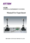
AT3000 (3CM)
WAVEGUIDE EXPERIMENT SYSTEM
Manual For Experiment
SHENZHEN ATTEN ELECTRONICS CO.,LTD.
1
Quality Assurance
SHENZHEN ATTEN ELECTRONICS Co., Ltd. guarantees quality of this product
As for the period to warrant the quality of this product, SHENZHEN ATTEN ELECTRONICS
makes it a rule to maintain such assurance for 2 years from the purchase date. If any failure is
found during this guaranteed period, please contact your sales representative if possible or
SHENZHEN ATTEN ELECTRONICS Co., Ltd. directly.
Cautions for Warranty
It is recommended for you to keep the followings when using this product so that you may be
covered by our quality assurance.
1. Before using the equipment, you should have full understanding about how to handle and use
the equipment as described in the manual.
2. Before connecting power, confirm if input voltage selected for the equipment is same as the
power voltage.
3. Rated fuse shall be used.
4. Do not use or keep this product under heat and humid condition.
5. SHENZHEN ATTEN ELECTRONICS Co., Ltd. is not responsible for assurance in the
following cases;
a. In case of damage caused by mistake or negligence, or remodeling its performance
b. In case guaranteed period is terminated (But, when guaranteed period is terminated, parts
supply or failure repairing is provided on charge. Such period is 5 years from the
termination of guaranteed period.
2
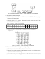
TABLE OF CONTENTS
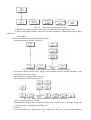
Chapter-1 Introduction
1-1 The module AT3000 3cm waveguide experiment system
1-2 Technical descriptions of components and instruments
Chapter-2 Usage
2-1 Cares for use
2-2 The way to use the component with IN/OUT directions
2-3 The way to use the component with directions
2-4 The way to use power meter (option)
2-5 The way to use a 1kHz sine-wave generator
Chapter-3 Experiments
Experiments 1: The Gunn oscillator
Experiments 2: PIN diode modulator and detector
Experiments 3: Propagation modes, wavelength and phase velocity in a waveguide
Experiments 4: Q and bandwidth of a resonance cavity
Experiments 5: Power measurement
Experiments 6: Standing wave ratio (SWR) measurement
Experiments 7: Impedance measurement
Experiments 8: Basic properties of a directional coupler
Experiments 9: Attenuation measurement
Experiments 10: Study of a waveguide Hybrid-T
3
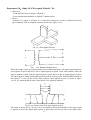
CHAPTER-1 INTRODUCTION
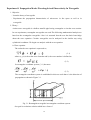
1-1 The Model AT3000 3cm Waveguide Experiment System
The AT3000 3cm waveguide experiment system is developed to provide with the users a
comprehensive way of understanding the basic properties of microwave frequencies and also
the easiest way of performing a number of microwave experiments using the popular X-band
frequencies (8.2--12.4 GHz).
The microwave radio communications network plays very important roll nowadays in our daily
life. For example, high quality long distance telephone calls, sometimes via communications
sattelites, are made possible using microwave telecommunications systems.
The superior characteristics of a microwave system comes from the fact that the microwave
frequencies have highly directional propagation properties which are similar to those of light.
Also, the high degree of noise immunity of the microwave frequencies in the atmosphere
makes the microwave communication the top choice in the long distance communications.
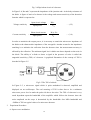
The AT3000 3cm waveguide experiment system, a very effective learning tool on the
properties of microwave frequencies, offers a variety of experiments centered around the
following key components involved in the microwave frequency oscillation, transmission
through antenna, and reception at the receiver.
Basic components included in AT3000 3cm waveguide experiment system.
1.Gunn Oscillator
10. Directional Coupler
2. Slide Screw Tuner
11. Horn Antenna (2EA)
3. Slotted Line
12. Hybrid Tee
4. PIN Modulator
13. Wave to Coax Adapter
5. Crystal Detector
14. Waveguide (2EA)
6. Frequency Meter
15. Reflector with Stand
7. Variable Attenuator
16. Power Supply
8. Fixed Attenuator
17. Coaxial Cable with Connector
9. Terminator
18. IKHz Square Wave Generator
Optional components available
1. Power meter with thermocouple;
2. SWR meter
4
1-2 Technical Descriptions Of Components Used In AT3000
1. Gunn Oscillator.
A Gunn oscillator, named after Gunn who
discovered the Gunn effect in 1963,
generates microwave frequencies when a
Gunn diode, which is loosely coupled to a cavity, is connected to a 8~10V DC power source.
The power output of the Gunn oscillator ranges from 5 to 20 milliwatts, depending upon the
supply voltage, and other parameters of the oscillator, It is recommended that output frequency
of X-Band of this manual's experiment procedures should be fixed 10GHz.
2. PIN-diode Modulator.
A PIN-diode modulator utilizes the property of a PIN diode which is
placed across a waveguide. If the PIN-diode is reverse
biased, he insertion loss of the diode is
so small that it does not affect the energy flow
inside the waveguide. However, when the reverse bias is
removed, either fully or partially, the diode begins to control the energy flow, thus creating an
amplitude or pulse modulation effect. Impedance matching is required to obtain the maximum
power output. Leaving the diode unbiased could be destructive to the diode when there is a signal
flow in the system.
3. Frequency Meter.
The basic working principle of the frequency meter in AT3000
comes from the high Q resonant characteristic of the resonant
cavity which is attached to a waveguide. The microwave signal
in the waveguide is coupled to the resonant cavity through a
small slot between the cavity and the waveguide. The
effective size of the cavity, and thus the resonant frequency of the
cavity, is variable by moving in and out an adjustable plunger which has a calibrated dial knob
assembly. When the resonant frequency of the cavity is equal to the frquency ofthe waveguide,
there is a maximum energy transfer from the waveguide to the cavity. This condition is indicated
5
by a large power drop on the power meter which is connected to the waveguide. The actual
frequency is obtained by reading the calibrated dial.
4. Thermocouple Power Meter (Optional).
A high quality thermocouple (high frequency materials for the thermo junctions with low error
rate) can convert the microwave energy to a readily measurable DC voltage. The DC voltage
can be easily amplified then fed to a meter. The meter indication is calibrated to represent
the power level in the waveguide.
Thermocouple Head Connection Cable Power Meter
5. Variable Attenuator.
A variable attenuator provides an attenuation by
varying the degree of insertion of a matched
resistive strip into a waveguide. The variable
attenuator is used to control a power level, or to isolate a source from a load.
6. Fixed Attenuator.
The purpose of the fixed attenuator used in AT3000 is
to provide a fixed attenuation of 20dB.
The attenuation is obtained by insertion of a thin
conducting absorber into a straight portion of a standard waveguide.
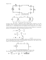
7.Directional Coupler.
The directional coupler, which allows directional coupling of energy in the waveguide is
basically a sampling device of the microwave signal. A directional coupler is consisted of two
waveguides combined together and coupled by holes at the joining section of the two.
Directional couplers are very popular in microwave systems where measurements of incident
and reflected power are needed to determine the Standing Wave Ratio or SWR. The directivity,
6
which is a figure of merit of a directional coupler, is a measure of how well the power can be
coupled in the desired direction in the neighboring waveguide. Usually, one end of the
neighboring waveguide containes a matched load which absorbs the energy headed towards
undesired direction. The directional coupler used in AT3000 has a coupling factor of l0dB (±
3dB) and a directivity of 40dB. A directional coupler is represented by a graphical symbol of
the following :
8. Slotted Line.
In measuring the standing waves inside a
waveguide, a slotted line is used to probe the
amplitude and the phase of the standing wave
pattern. Obtaining the standing wave pattern
information allows us to determine the wavelength,
standing wave ratio and the impedance of the transmission line. As the name implicates, a slotted
line has slot along the center line of the broad side of the wall. An assembly . consisting of a
probe and a crystal detector ,is designed to slide along the open slot and as it does, the probe
samples the field in the waveguide, while the crystal detector provides a rectified signal. The
depth of the probe into the waveguide is adjustable and the strength of the detected signal is
proportional to the depth. The user should be aware of an optimized depth in use of a slotted
line since too shallow depth would make the detected
signal too weak and too deep depth would
substantially reduce the main signal power in the waveguide and may even cause field distortion.
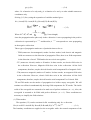
9. Slide Screw Tuner.
The primary use of the slide screw tuner is to match
loads, detectors, or antennas to the characteristic
impedance of the waveguide. The mechanical
structure of a slide screw tuner consists of a probe
7
mounted on a carriage which slides along a narrow and long slot on the feeding waveguide.
When the Adjusting micrometer is turned, the depth of the probe varies. The combination of the
depth and the position of the probe causes reflection in the waveguide at a specific amplitude and
phase.
Relation between probe's depth and micrometer's scale [unit : mm]
micrometer's
3
5
7
9
7
5
3
0
scale
probe's depth
10. Crystal Detector.
The crystal detector is located inside the waveguide
walls which is joined to a coaxial connector.The crystal
detector is basically a diode assembly which responds
to the electromagnetic field inside the waveguide.
The diode assembly is consisted of a small thin piece of silicon,
a thin tungsten wire and a case. One side of the silicon is directly connected to the case and the
other side is connected to the tip of the tungsten wire. The diode action is due to the different
properties of silicon and tungsten; silicon has few surplus electrons but there are many free
electrons in tungsten. Therefore, when a voltage is applied across the diode in such a direction
as to force electrons to leave silicon and enter tungsten, a very small current results. In contrast,
when the direction of the voltage is reversed, a large current flows from tungsten into silicon.
This is how the diode can be used for detection of microwave energy. The diode is a fragile
device; it can be easily damaged from an excessive voltage. The characteristic of a crystal
detector (or the relationship between the output voltage and current to the input voltage) is such
that the device follows a square law ~ within a certain range of input power. The square law
characteristic means the output voltage is proportional to the square of the input voltage.
can also be said that the output voltage is directly proportional to the input power.
11.Matched Terminator.
The matched terminator is essentially a matched
load to a microwave transmission line. As the standing
8
It
waves occur due to impedance mismatches in the system,
the matched terminator is used to minimize the SWR in a system.
12. Coaxial Adapter.
Provides a match between a waveguide and a 50 ohm
coaxial line. The power flow can be in either direction.
However, SWR in the adapter should be kept less than 1.2.
13. Magic-Tee (or Hybrid-Tee).
A magic-Tee is a four port device which is basically
a microwave version of a hybrid coil of the type
commonly used in telephone repeater circuits.It has
the properties that, when properly terminated in external
impedances, power incident on any arm splits equally between the two adjacent arms, but there
is no power coupled to the opposite arm. The magic-Tee is an essential device in balanced
mixers, automatic frequency control circuits and impedance measurement circuits.
14. Reflecting Sheet.
A mean of reflecting electromagnetic waves in free
space when measuring the wavelength of a signal.
15. Shorting Plate.
When measuring the wavelength inside of a waveguide,
a shorting plate is used to create a short (zero impedance)
at the open end of a wave guide.
16. Waveguide Straight Section.
A six inch straight section of waveguide used in
measurements of the wavelength and the phase velocity inside a waveguide.
9
CHAPTER-2 USAGE
2-1 Cares For Use
1. In order to improve the measuring reliability, the connection of each micro waves should be
made correctly and should adhere to the following rules.
◆The central rectangle of waveguide should be kept in a line and the edge should be matched.
◆Two flange should be tightly jointed with four screws and nuts so that the micro wave doesn't
leak.
2. The components of this experiment set should not be used for any other experimental purpose.
3. No drop or shock should be applied to every component.
4. Keep away from humidity or heat.
5. Should avoid to use in a dusty area and should be kept in its storage case after use.
6. Check whether any foreign substance is attached on the entry/exit of waveguide before the
assembly for the experiment circuit construction of components and remove the foreign
substance if existing.
7. While the oscillator is oscillating, the internal part of oscillator must not be observed through the
output part.
Because the oscillator used in this experiment unit a relatively small power, the output is not
dangerous to other body parts, but eyes can be permanently damaged.
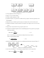
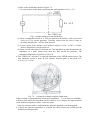
2-2 The Way To Use The Component With IN/OUT Directions
Among the 15 kinds of microwave components within AT3000, the input and output of wave
course is classified as in the following.
◆Slide Screw Tuner
◆Slotted Line
The above two kinds hold the sliding location of 0~40. Since the flange with "0" on this
adjustment scale becomes input and the flange with "40" scale becomes output, the connection
should be made correctly according to the experiment and route.
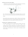
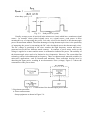
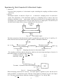
The following picture shows a connection example of Slotted Line.
10
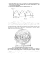
2-3 The Way To Use The Component With Directions
Among microwave components, there are components which
has the pre-set connection
direction. These components are not transmitted in one certain direction and send the wave only
to a specific direction. The following components are these.
◆ Directional Coupler
◆ Magic-Tee (also called as Hybrid Tee)
The following picture is an example of using a directional coupler and the arrows indicate the
possible wave directions.
The directional coupler of picture(a) shows that in the case that the wave enters to Pl, the same Pl
wave is transmitted to P2 and P3. However, picture(b) shows an opposite case of (a) which the
wave enters through P2. Although this wave is transmitted to P1 from P2, it is not transmitted to
P3.If using these characteristics, one M/W antenna can be made for transmission and reception
and the reflection wave in the waveguide circuit can be detected.
Experiment-10(EXT.-10) provides the detailed information about Magic-Tee component.
Please refer to Experiment-10.
11
2-4 The Way To Use Power Meter (Option)
AT3000 Microwave Trainer provides the M/W Power Meter Model PM-3001. The following
picture shows an example of using the Thermo Couple Power Meter PM-3001.
[Note]
PM-3001 Power Meter measures up to several 1μW through a thermo probe. If the RF
power over 1W is directly measured without attenuation, the M/W detection thermo probe may be
damaged.
PM-3001 holds the frequency measurement range of 10MHz~12.4GHz and is made of three range
like0.1mW, 1mW and 10mW. Therefore, when initially measuring, measure by setting the 10mW
range and gradually select a lower range according to the indication sensitivity of meter.
2-5 The Way To Use A 1kHz Sine-Wave Generator
This oscillator, by applying the sine-wave bias voltage of 1kHz to Pin Modulator, make possible
to give a sine-wave alteration to the microwave. This alteration is helpful to various
measurements such as its specific experiment practice of a simple alteration, measurement of
phase changes within a waveguide circuit, measurement of reflection wave, and measurement of
attenuation amount. The following shows a connection example of Pin Modulator and 1kHz
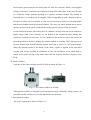
sine-wave oscillator.
12
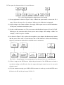
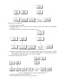
1. Pin Modulator
11. Wave guide
2. Slotted Line
12. Fixed Attenuator
3. Magic-Tee
13. Terminator
4. Variable Att
14. Frequency Meter
5. Crystal Detector
15. Shorting Plate
6. Coaxial Adapter
16. 1kHz Generator
7. slide Screw Tuner
17. Cord/Screw
8. Directional Coupler
18. Power Supply
9. Gunn oscillator
19. Reflector Stand
10. Horn Antenna
20. Component Supporter
13
CHAPTER-3 EXPERIMENTS
(LIST OF REQUIRED EQUIPMENT FOR PERFORMING EXPERIMENTS)
1. GUNN OSCILLATOR
2. PIN-DIODE MODULATOR
3, POWER SUPPLY AND SIGNAL SOURCE
4. OSCILLOSCOPE (DUAL TRACE)
5. S.W.R METER
6. FREQUENCY METER
7. THERMOCOUPLE MOUNT POWER METER
8. VARIABLE ATTENUATOR
9. FIXED ATTENUATOR
10. DIRECTIONAL COUPLER
11. SLOTTED LINE
12. SLIDE SCREW TUNER
13. CRYSTAL DETECTOR
14. MATCHED TERMINATOR
15. WAVEGUIDE-TO-COAX ADAPTER
16. HYBRID-TEE
17. REFLECTOR WITH STAND
18.SHORTING PLATE
19. WAVEGUIDE (STRAIGHT SECTION)
20. DVM
14
Experiment 1: The Gunn Oscillator
1. Objectives:
The objectives of this experiment are to obtain the knowledge on the! theory and the operation
of the Gunn oscillator as a source of microwave frequencies.
2. Theory:
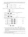
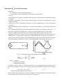
A. The Gunn Effect.
The Gunn effect, or the transfered electron effect, which was discovered by Gunn in 1963
states that when a small DC voltage is applied across a thin slice of semiconductor materials
as illustrated in Figure 1-1, it exhibits negative resistance under certain conditions Gunn used
in his case gallium arsenide(GaAs) and indium phosphide (InP). Once the negative resistance
is developed, one can easily generate oscillations by connecting the negative resistance
element to a tuned circuit.
One of the requirements in maintaining the negative resistance state in the semiconductor
materials is to keep the voltage gradient across the material over 3000V/cm. The most
appropriate tuned circuit to be connected the semiconductors for microwave frequencies is a
tuned cavity.
Fig. 1-1 The side view of an epitaxial GaAs Gunn semiconductor
The Gunn effect, which takes place only in n-type semiconductor materials, is a result of the
property of the semiconductor itself. It is found that any parameters associated with junction
or contact properties as well as voltage or current do not affect the Gunn effect. Only the
electric field is required to be above the threshold to maintain oscillation. The Gunn diode is
insensitive to the magnetic field and thus it does not respond to any incident magnetic field.
The frequency of oscillation is mainly determined by the time the electrons, in a form of a
bunch, take to traverse the given slice of material.
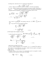
B. Negative resistance and transfered electron effect.
15
The energy bands and energy levels of GaAs is shown in Figure 1-2. Notice that this material
possesses an empty energy band at the top of the energy level. The partially filled energy
band is bellow the empty band. When the material is doped with n-type material, there are
excess electrons in the material ready to flow when a voltage is applied across the diode.
Fig. 1-2 The energy levels in a GaAs Gunn
The current flowing in the diode is proportional to the voltage, and the current is oriented
toward the positive end of the GaAs. The situation of the higher the voltage, the larger the
current is equivalent to positive resistance. However, when the level of the applied voltage
reaches a sufficiently high value, electrons, instead of trying to travel even faster, transfer to
the higher energy band which is empty and less mobile. As a result, the current flow
decrease exhibiting negative resistance phenomenon.
The electron transfer from a lower energy level to a higher level is called transfered electron
effect. If the voltage level is increased even further, the mobility of the electrons in the higher
energy band begins to improve, resulting in an increased current.
C.Gunn Domains.
The frequency, of the oscillations in the GaAs has to do with the formation and the transit
time of the electrons which form themselves in "electron bunches". The negative resistance
effect is an important factor in understanding the Gunn oscillator, however,
the negative
resistance effect alone does not explain everything that is happening inside the oscillator. The
other important element is the formation of domains, or Gunn domains. The amount of free
electrons available in the GaAs depend upon the density of the n-type material doped in the
GaAs. Since the density of doping is not necessarily uniform across the GaAs, there are fewer
free electrons where the doping density is low.
Fewer free electrons mean less conductivity and, therefore, the potential difference in such an
16
area becomes greater than the area where there are more free electrons. Hence, as the applied
voltage is increased, eventually the transfered electron effect takes place at this area first due
to a sufficient voltage gradient, resulting in a negative resistance domain. The domain as
described above is considered to be unstable. What is happening in such a domain is that as
electrons are taken out of circulation at a fast rate, the elctrons in front travel forward rapidly
and the ones behind bunch up(electron bunches). This way, the whole domain moves across
the slice and toward the positive and with an average speed of about 107cm per second.
As the transfered electron effect takes place in a domain, moving electrons to less conductive
higher energy band, fewer electrons are left behind in the conduction band, making this
region less conductive at this time. As was explained in the previous section, this causes the
potential gradient to increase, making the domain capable of traveling. Thus, this process of
electron transfer and domain traveling repeats itself and is said to be "self perpetuating".
When the domain reaches to the anode of the diode, a pulse is applied to the associated
resonant tank circuit, resulting in oscillations. In fact, the oscillations of the Gunn diode is
caused by the pulse arriving at the anode rather than the negative resistance property of the
diode.
D. Gunn Oscillator.
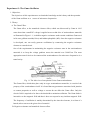
A picture of the Gunn oscillator used in AT3000 is shown in Figure 1-3.
Fig.1-3. The Gunn oscillator in AT3000.
Although the oscillator is designed to prevent spurious mode oscillations, tuning features are
provided with the oscillator in case fine adjustments are necessary.
3. Experiment Procedure.
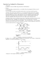
Set up the equipment as shown in Figure 1-4.
17
Fig. 1-4 Setup for measuring the current vs. voltage characteristic of the Gunn diode
A. The current vs, voltage characteristic.
(1) Set the voltage to 4 volts. Set the variable attenuator to 10dB.This will ensure proper
isolation to the Gunn oscillator.
(2) Raise the voltage in 0.5V increment. Measure and record the current each time in Table
1-1. Caution: Do not exceed 10V.
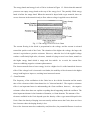
Table 1-1 Current vs. Voltage of the Gunn diode
Voltage(V)
4.0 4.5 5.0 5.5 6.0 6.5 7.0 7.5 8.0 8.5
9.0 9.5 10
Current(mA)
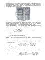
(3) Reduce the voltage to 0V. From Table 1-1, construct a V-I curve as suggested
in Figure 1-5.
Figure 1-5. Current vs, Voltage characteristic of Gunn diode
B. Measurement of the oscillator output power vs. supply voltage.
(1) Turn the power meter on and calibrate the power meter to zero.
(2) Raise the Gunn diode voltage in 0.5V increment and record the power indication on the
power meter and the attenuator setting.
(3) Convert the obtained power reading in miliiwatts to dBm. Then add the attenuation (in dB)
18
to the dBm.
Example: Assume the power reading is 6.3mW with the supply voltage of 8.5V. Then the
power in dBm=l0log 6.3=8dBm. Add 3dB attenuation to 8dBm. The total power is
11dBm. Now convert the11dBm which is the Gunn diode output power back to the
milliwatts:
(4) Repeat step (3) and complete the Table 1-2.
Table 1-2. Data for the supply voltage and the output.
Voltage(V)
+4V
+4.5V
power meter meter(mW)
power (dBm)
attenuator (dB)
Gunn diode(dBm)
Gunn diode (mW)
(5) Draw a graph showing the relationships between the supply voltage and the output
power.(Figure 1-6).
Fig. 1-6. Gunn diode supply voltage vs. output power characteristics.
C. Measurement of the oscillator output frequency vs. supply voltage.
(1) Set up the equipment as shown in Figure 1-7. Set the supply voltage to 9V. Set the
attenuator to the maximum attenuation. Switch the power meter to1.0range. Reduce the
attenuation untill the power meter reading is close to the right side of the meter scale
(approximately 0.8 to 1mW).
19
Slowly turn the frequency meter. Observe a dip on the power meter when the frequency
meter is exactly same as the frequency of the Gunn oscillator.
(2) From the lowest supply voltage at which oscillations occur to the
maximum of 10V supply voltage, vary the voltage in an increment of
IV. Each time, fill in the Table I-3. Notice that the frequency
meter is calibrated in 10MHz increment.
Fig. 1=7. Setup for measuring the oscillator output frequency vs. supply voltage.
Table1=3.
Supply voltage vs. measured frequncy.
voltage (V)
Measured frequncy (MHz)
20
Experiment 2: Modulator And Crystal Detector
1. ObJectives:
- Learn the basic theory and the operation of the PIN diode modulator
- Learn the basic theory and the operation of the crystal detector
2. Theory:
A. PIN diode
As is shown in Figure 2-1(a), the PIN diode is constructed with a thin insulator sandwitched
etween P and N materials, hence the name PIN diode. The thickness of the P and N is much
heavier than the insulator. In case of reverse bias condition, the PIN diode is a high resistive
and capacitive device in the microwave frequency. It is an avalanche effect device; under a
orward bias condition, an avalanche effect takes place in the insulator, allowing holes from P
and electrons from N to flow. Thus, the insulator becomes effectively conductive.
An equivalent circuit of a PIN diode is shown in Figure 2-1(b).In Figure 2-1(c) and (d), the
equivalent circuit is modified to indicate the results of biasing.
(a) constructed
(b) equivalent circuit
(c) reverse biased
(d) forward biased
Fig. 2-1 The construction and equivalent circuits of a PIN diode
The PIN-diode modulator has a diode connected across a waveguide. The diode functions as a
21
modulator when the biasing conditions vary due to a sufficiently large squarewave (low
requency) signal applied across the diode under the presence of a microwave signal inside the
waveguide. When the diode is reversed biased, it does not affect the energy flow. Full or partial
removal of the reverse bias allows the diode to control the energy flow.
This type of modulator, using an insulator junction between p and N, offers excellent
modulation characteristics due to the minimized rectification activities and harmonics
generation during the modulation process.
B. Crystal detector.
The crystal detector is a device capable of detecting microwave signals based on the "square
law" characteristics. Point contact germanium or silicon crystal diodes are the most popular
type of crystal detectors. Sometimes, a bolometer is used for microwave detection, although
the device is mainly intended for microwave power measurements.
A typical crystal detector circuit and associated characteristic curves of a crystal detector are
presented in Figure 2-2 and Figure 2-3(a)and(b). In figure 2-2, the two filters (input high-pass
and output low-pass) are to separate the microwave frequencies from the DC output.
Fig. 2-2 Typical crystal detector circuit
Fig. 2-3 The V-I characteristics of a crystal diode
22
In Figure 2-3, we are interested in finding the relationship between the diode current and the
diode voltage. In general, the curves like the one in Fifure2-3 can be approximated by the
Taylor series expressed in terms of the powers of the voltage;
…..(2-1)
Normally, the first three terms are sufficient to approximate the entire function. If the voltage
is expressed as:
V= Acosωt;where A is the amplitude and ω is equal to 2πf
Substituting V into (2-1) yields :
i= a0+a1(Acosωt)+a2(Acosωt)2+…..
Using
cos2ωt=
1
…..(2-2)
…..(2-3)
(1+cos2ωt)
2
a2A2
i= a0+a1(Acosωt)+
(1+cos2ωt)+….
…..(2-4)
2
Now, the characteristics of the square-Jaw becomes clear. In equation(2-4), the DC component
is contained in the
term. The second harmonics is expressed as
. Therefore, we
can say that the current in the detector is proportional to the square of the amplitude A of the
microwave voltage. This concept is only valid up to a certain signal level. At higher signal
level, more terms may be needed in (2-4) and the diode is no longer considered as a square-law
device.
In addition to the detector circuit of Figure 2-2. the diode itself can be expressed in terms of an
equivalent circuit. In Figure 2-4, a complete equivalent circuit of a detector is presented.
23
Fig. 2-4 Equivalent circuit of a detector.
In Figure 2-4, Ro and C represent the impedance of the junction and r is the body resistance of
the diode. A figure of merit of a detector is the voltage and current sensitivity of the detection
function which is expressed as:
Open circuit voltage
Voltage sensitivity
=
RoIdc
=
Input power
Short circuit current
Current sensitivity
…..(2-5)
Pin
=
Ro/(r+ Ro)
=
Input power
…..(2-6)
Pin
In order to maximize the output power, it is necessary to match the microwave impedance of
the diode to the characteristic impedance of the waveguide. Another reason for the impedance
matching is to minimize the reflection from the detector since the measurement accuracy is
affected by the reflection. The mininum signal level a diode can detect depends on the noise in
the diode. The ability of a diode to detect a signal in the presence of noise is called the
tangential sensitivity (TSS) of a detector. A graphical illustration of the concept of TSS is
sketched in Figure 2-5.
Fig.2-5 The TSS of a diode.
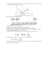
In Figure 2-5, a microwave signal which is pulse modulated is detected, amplified and
displayed on an oscilloscope. The real meaning of TSS is there has to be a minimum
microwave power level to make the pulse ride above the noise. The TSS of a detector is very
much dependent upon the bandwidth of the amplifier which follows the detector since the
noise amplitude on the scope is determined by the bandwidth. One MHz bandwidth and
-50dBm of TSS are typical values of a microwave detector.
3.
Experiment Procedure.
A. Square wave modulation.
24
Fig. 2-6 Setup diagram for square wave modulation.
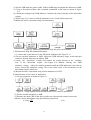
(1) Set up equipment as shown in Figure 2-6.
(2) Apply +9v to the Gunn oscillator.
(3) Set the variable attenuator to 10dB.
(4) Adjust the square wave generator to 1KHz and 2Vp-p output. Connect the generator to the
PIN modulator.
(5) Adjust the scope so that the top of the square wave aligns to the zero level on the screen.
(6) Adjust the attenuator so that the bottom of the square wave aligns to the zero level on the
screen.
(7) Repeat above measurement for lVp-p negative square wave.
(8) Calculate the modulation depth for the two modulating inputs of 2Vp-p and 1Vp-p using the
following equations.
Vmax
AdB=20log(
…..(2-7)
)
Vmin
where A is the difference in the attenuator settings between step(3) and (6).
where m is the modulation depth.
Vmax/ Vmin-1
m=
.…..(2-8)
Vmax/ Vmin+1
A sketch of the waveforms of the square wave modulation and detection is shown in Figure 2-7.
Figure 2-7.
Square wave modulation and detection
As one can see from Figure 2-7, the attenuator setting deviation A can be expressed as.
Pmax
AdB=10 log
Vmax
=20 log
Pmin
Vmin
25
…..(2-9)
B. The square law characteristics of a crystal detector.
Fig. 2-8(a) Setup diagram for output power level setting
(1) Set up equipment as shown in Figure 2-8(a). Calibrate the power meter to zero at the X0.1
range. Observe the meter for a few minutes. Make sure the calibration is maintained.
(2) Apply voltage to the Gunn oscillator. Also apply 1KHz square wave to the PIN modulator.
At this point, modulation should take place.
(3) Set the variable attenuator to 0. The power meter should indicate between 0.02 and 0.15mW.
Refering to the conversion table on the power meter, change mW reading to dBm. For
example, 0.1mW is equal to -10dBm.
(4) As shown in Figure 2-8(b), replace the waveguide to coax adapter, the thermocouple mount
and the power meter with a crystal detector and a SWR indicator. AdJust the modulating
frequency such that the deflection of the SWR meter is maximized.
Fig. 2-8(b)
Setup diagram for measuring square law characteristics of a crystal detector.
(5) Select a range on the SWR meter. Adjust the gain control of the SWR meter to obtain a
convinient reading on the dB scale. Once the range and the gain control are set, do not touch
the gain control.
(6) Vary the attenuator setting up to 20dB in IdB increment. At each step, record the SWR meter
deflection (in dB) and the gain range in Table 2-1.
26
Table 2-1 Input power vs, attenuation and SWR reading. (Accuracy:±2dB)
A
dB
SWR-INDICATOR
DEFLECTION
INPUT
POWER
DEFLECTION
RANGE
AND RANGE
dBm
dB
dB
dB
27
Experiment3: Propagation Modes Wavelength And Phasevelocity In Waveguide.
1. Objective :
- Learn the theory of waveguide.
- Experiment the propagation characteristics of microwave in free space as well as in
waveguide.
2. Theory :
A microwave waveguide is a hollow metallic pipe having rectangular or circular cross section.
In our experiments, rectangular waveguides are used.The following mathematical analysis are
based on the rectangular waveguides. Also it is assumed that the user has basic knowledge
about the wave equation. Circular waveguides can be analyzed in the similar way using
cylindrical coordinate. We begin our analysis with the wave equation.
A. Wave equation.
The reduced wave equation is expressed as ;
(3-1)
where (x,y,z) is the scalar wave function and k, the wave number is defined as
(3-2)
In rectangular coordinate system, (3-1) becomes:
(3-3)
The rectangular coordinate system is established in this case such that z is the direction of
propagation as shown in Figure 3-1.
Fig. 3-1 Rectangular waveguide in rectangular coordinate system.
Our goal is to obtain a solution which has a form of
28
…..(3-4)
g(x,y) f(z)
where f is a function of z only and g is a function of x and y or other suitable transverse
coordinates only.
Solving (3-3) for φ using the separation of variables method gives:
Φ={A1cos(KxX)+A2sin(KxX)}{B1cos(KyX)+B2sin(KyX)}
….(3-5)
Where Kx2+Ky2=K2 and
(βg=2/wavelength)
since the propagation takes place only in the z-direction. A wave propagating in the positive
z-direction is represented by e
-jβgz
-jβgz
and therefore, e
corresponds to a wave propagating
in the negative z-direction.
Three types of propagation modes are of particular interest for us:
- TEM (transverse electromagnetic) modes: In these modes, both electric and magnetic
fields are transverse to the direction of propagation. Thus, there is no field components
in the direction of travel. TEM modes do not exist in waveguides.
- TE {transverse electric) modes or H-modes: In these modes, no electric field exists in
the z-direction. However, Magnetic field does exist in the z-direction. All the field
components, therefore, maybe derived from the axial component Hz of magnetic field.
- TM (transverse magnetic) modes or E-modes: In these modes, no magnetic field exists
in the z-direction. However, electric field does exist in the z-direction. All the field
components, therefore, maybe derived from the axial component Ez of electric field.
TE and TM modes are the modes of propagation in a hollow empty waveguide. We will
continue our efforts in mathematically deriving field components for TE modes. The inside
walls of the waveguide are assumed to be made out of perfect conductor (σ = ∞), Also, the
waveguide is assumed to be filled with perfect dielectric ( σ = 0 ). These conditions are
necessary to simplify the field solutions.
(1) TEmn modes.
The equation (3-5) can be rewritten for Hz. considering only for +z direction.
Hz=(A1cosKxX+A2sinKxX)( B1cosKyX+B2 sinKyX)(C1e-jβgz)=De-jβgz
……(3-6)
The boundary conditions are applied at the waveguide walls: the normal component of the
29
transverse magnetic field must vanish at the perfectly conducting waveguide walls. Also,
tangential electric field also vanishes on the waveguide walls. Then, the requirements on "D"
as was defined in (3-6) are
… ..(3-7)
…..(3-8)
Applying (3-7) and (3-8) to (3-6) specifies the values of the characteristic constants Kx and Ky.
nπ
a
mπ
Ky=
a
Kx=
n=0,1,2,….
m=0,1,2,….
Using the above relations and substituting AIBI = Anm, the solutions for "D" are:
nπY
nπX
D=Anm cos
cos
…..(3-9)
a
b
For n=0,1,2,…. ; m=0,1,2,…. ;and n=m≠0
The final form of Hz is now,
nπY -jβgz
nπX
Hz=Anm cos
cos
e
…..(3-10)
a
b
The associated transverse E and H fields are obtained from (3-10) and the Maxwell's
equations in rectangular coordinates :
nπX
nπY
jωμmπ
Ex=
Anm cos
sin
e-jβgz
…..(3-11)
2
Kc b
a
b
-jωμnπ
nπX
nπY
Ey=
Anm sin
cos
e-jβgz
…..(3-12)
2
Kc b
a
b
jβgnπ
nπX
nπY
Anm sin
cos
e-jβgz
…..(3-13)
Hx=
2
Kc b
a
b
jβgmπ
nπX
nπY
Anm cos
sin
e-jβgz
…..(3-14)
Hy=
2
Kc b
a
b
It should be noted that
Kc2=(
nπ 2
nπ 2
) +(
) =
a
b
the cutoff wave number for the nm-th mode. Also,
and n=m≠0
The significance of the integers n and m : the value of n or m indicates the number of
half-cycle variations of each field component with respect to X and Y. Another words,
each combination of m and n values represents a different field configuration (or mode}
in the waveguide.
(2) TM modes : Very much the same steps are required to obtain field solutions for TM
modes except that this time. Hz must be set to zero.
B. Characteristics of rectangular waveguide.
(1) Cut off frequency and cut off wavelength.The exponential form of e-jβgz represents a wave
30
traveling in the +z direction. Let us re-examine the relationship of
i) K>Kc : Theβg is real and e-jβgz is indeed traveling in +z direction (propagating).
ii) K <Kc : Theβg is imaginary and the propagation mode decays rapidly with distance z
in the +z
direction, resulting in propagation cut off. The frequency separating the
propagation and no-propagation is called the cut-off frequency, Since ωc=2πfc,
….(3-15)
Also, from K=
and replacing withω=2πf
和
, then K=
,Letλc be the cut-off wavelength when K=Kc:
…..(3-16)
(2) Wavelength in the rectangluar waveguide.
and
Letλgbe the guide wavelength, From
……(3-17)
……..(3-18)
whereλis the wavelength in free space.
In order to support propagation in the waveguide, λ<λc (λc is required).This implies to
the fact that λg is greater thanλin the waveguides. Another words, the guide wavelength is
longer than the wavelength in the free space.
(3) Phase velocity.
The phase velocity, or the velocity of a constant-phase point in waveguide is readily
obtained from the frequency and the guide wavelength:
…….(3-19)
31
It should be noted from (3-19) that the phase velocity in the waveguide can exceed the
speed of light in free space which is 3 x 10⁸u/sec.
3. Experiment procedure.
Set up equipment as shown in Figure 3-2.
Fig.3-2. Equipment setup for measurements of frequency, λgandλ.
A. Frequency measurement.
(1) Apply voltage to the Gunn oscillator. Also apply 1KHz, 2Vp-p square wave to the PIN
modulator.
(2) Adjust the variable attenuator to 10dB. Set the SWR meter such that the meter indicates
approximately the middle of the scale.
(3) Adjust the frequency of the square wave generator so that the SWR indication is
maximized.
(4) Turn the frequency meter untill there is a significant drop on the SWR indicator. Record
the frequency in Table 3-1. De-tune the frequency meter.
B. Measurement of free space wavelength and guide wavelength
(1) When the reflecting sheet is moved toward the open end of the waveguide, with the
reflecting sheet oriented to the waveguide with right angle, then the standing wave
pattern should vary due to the reflections from the plate. This variance of the standing
wave is detected by the probe in the slotted line. Find two adjacent positions where the
two detected values are minimum. The distance between these two points corresponds to
the half wavelength in free space. Record the distance in Table 3-1.
(2) Cover the output of the slotted line with the shorting plate.Vary the slotted line and locate
a position where the detected output voltage is minimum. From that point, find another
adjacent point where a minimum is detected again. The distance between two points is
the half of the guide wavelength. Record the value in Table 3-1.
Table3-1. Comparison of measured and calculated values of frequency,
free space wave length and guide waveleagth
frequency
Measured values
λ
Measured values
λg
Calculated alues
λ
calculated values
λg
32
Experiment 4:Q Value And Bandwidth Of A Resonance Cavity
1. Objectives :
- Learn the theory of a resonance cavity.
- Experiment the relationship between Q and bandwidth. Learn how to measure the fl of a
resonance cavity.
2. Theory.
Resonant circuits are of great importance for microwave oscillators, tuned amplifiers and
frequency measurements, etc. A resonant circuit such as the one shown in Figure 4-1can be
defined in terms of R, L,C
when the frequency is limited up to approximately 100 MHz.
Figure 4-1
A resonant circuit.
In fig.4-1
…..(4-1)
where Ro is the parallel equivalent resistance.
ωo is the resonant frequency.
Qo is the Q of the resonant tank.
….(4-2)
From(4-1),
When the R,C and L are know, ωo, Qo and Ro can be easily calculated.
However, in microwave circuits, the analysis of the resonant cavity becomes difficult due to
the extremly high value of Q. The other characteristics of the microwave resonator which make
the analysis difficult are:
- the circuit parameters vary depending upon the propagation modes.
- Unlike the low frequency case, the meaning of the voltage and the current in the tank
becomes ambigious, making the definition of Ro difficult.
Usually the Ro is defined in microwave as:
……(4-3)
where E is the maximum potential between two points in the cavity and W is the power
dissipated in the cavity. The ωo, Qo and Ro of simple cavities can be found from the
dimensions of the cavity and the power loss on the cavity walls. However, due to the
complexity of the cavity structure, it is almost impossible to calculate ωo, Qo and Ro. Instead,
actual measurements of a few parameters of the cavity make it possible to determine the entire
characteristics of the device.
Let's consider a cavity system in Figure 4-2 (a).
In Figure 4-2(a), Z01 is the characteristic impedance of the input waveguide. Z02 is the
characteristic impedance of the output waveguide. Rg is the internal resistance of the generator.
RL is the load resistor.
An equivalent circuit of Figure 4-2(a) can be developed by lettingZ01 = Rg, Z0z = RL. See
33
Figure 4-2(b).
Fig. 4-2 (a).
A transmission cavity
Fig. 4-2(b). An equivalent circuit of Fig. 4-2(a).
In Figure 4-2(b), the cavity is effectively a series resonant circuit coupled by two ideal
transformers with 1:ni and n2:l turns ratio. The output power in this case is Po = Ey2 / 4Zo. A
resonant curve is a relationship between the frequency and the output power of a resonant
cavity, Consider two points on the resonant curve like the one shown in Figure 4-5. Assume the
points are several dB below where the maximum output power occurs.
∵
…(4-4)
where F is the ratio between the maximum power and the power of the two points on the curve.
Δf is the bandwidth of the cavity. α is the bandwidth coefficient.The cavity portion of the
Figure 4-2(b) is presented in detail in Figure4-3.
Fig. 4-3 Equivalent circuit of the cavity portion of Figure 4-2(b).
The following relationships are obtained by carefully observing Figure 4-3.
, since
34
….(4-5)
=
Where
and
The impedance of the equivalent circuit is
….(4-6)
The power delivered to the load is
…..(4-7)
At resonance,the imaginary portion of(4-6)becomes 0.
……(4-8)
The bandwith of the resonant circuit is defined as the difference of two frequencies where the
maximum power is reduced to one half.This happens when
……(4-9)
where Δf is the half-power bandwidth.
3. Experiment procedure.
A. Measurement of Q values using the power measurement technique.
Fig. 4-4. Setup diagram of 0-measurement.
(1) Set up equipment as shown in Figure 4-4.
(2) Apply voltage to the Gunn oscillator. Set the range switch of power meter to xlmW. Adjust
the variable attenuator for the maximum meter deflection. Refer this value as P0.
(3) Turn the frequency meter slowly and find the power and frequency reading when the power
meter reading is minimized. Call these values PB for power and fo for frequency.
35
(4) Slowly rotate the frequency meter, Find two frequencies (fl and f2) where the power
reading is equal to ΔP/2 (see Figure 4-5).
Fig.4-5. The resonant curve of a resonant cavity.
B. Measurement of Q using SWR method.
Fig.4-6. Setup diagram for the measurement of Q using SWR method.
(1) Set up equipment as shown in Figure 4-6.
(2) Turn the Gunn oscillator on and set the attenuator to 10dB.
(3) Adjust the range switch and the gain adjust to obtain 0dB on the SWR meter.
(4) Slowly rotate the frequency meter. Find the point where the SWR meter reading is
minimum. Read the dB indication on the meter (P).
(5) Plug-in the value obtained from (4) into the following equation to get the ratio Ps.
(6) SinceΔP=1-PB, calculate PB + ΔP/2 and convert it to dB. example :
(7) Slowly rotate the frequency meter and find fl, f2 and△f where the SWR meter reading
indicates X dB as calculated above.
36
Experiment 5:Power Measurement
1.Objectives.
-Learn different ways of measuring power.
-Learn how to evaluate the accuracy of the power measurements.
2. Theory.
In general, the term "power" is defined as the time rate of transferring or transforming energy.
In case of
microwave, the energy is used in many different forms: exchange of information over long
distance, heating
a microwave oven, or acceleration of particles in nuclear engineering, etc. The most common
practice of
power measurement at low frequencies is to measure the voltage an the current of the device
under
test, then calculate the power from the lumped value of the circuit parameters. However, at
microwave frequencies, the difficulty arises due to the distributed nature of the circuit
elements. Another factor affecting is the reflection of the signal at whereever there is an
impedance mismatch. Two types of power measurements are involved in the microwave power
measurements ; average power or peak power measurement. The average power is the time
average of the sum of the product of the instantaneous voltage and current over the time period.
This relationship is illustrated in Figure 5-I and a mathematical expression is given in (5-1).
Fig.5-1. Instantaneous power appearing at the load resistor
…….(5-1)
where T = period
e = instantaneous voltage
i = instantaneous current
It should be noted in Figure 5-I that the frequency of the instantaneous power (Pinst) is two
times of the frequency of e and i. The average power in an alternating current circuit is expresse
as:
Pagv=ERMS · IRMS · Cosθ
…….( 5-2 )
whereθis the phase angle between E and I.。
Now, consider a duty cycled pulse as shown in Figure 5-2. The peakpower of the pulse is related
to the average power of the pulse by the duty cycle of the pulse.
37
where duty cycle = τ /T
Fig. 5-2. Peak power of a pulse
Usually, average power is involved in the microwave circuit which has a contineous signal
source. In contrast, where pulsed signals serve as a signal source, peak power is more
meaningful way of expressing the power. Let's take a look at the details of the thermocouple
power measurement method. The main advantage of using thermocouple wires is the possibility
of measuring the power by measuring the DC volts developed across the thermocouple wires.
The DC voltage is generated as the wires conduct the high frequency current and heat is
generated across the two different metal contacts. In contrast, a power meter works as the
voltage is applied to a meter and the meter is calibrated to indicate the power. The usability of
the thermocouple wires used to be limitted to low frequencies. However. The recent thin film
technology offered a breakthrough in frequency. There are thermocouple materials suitable for
microwave applications, such as bismuth and antimony. These materials develop heat by
absorbing the input power, resulting in an electromotive force (voltage). Figure 5-3 shows the
construction of the power meter.
Fig. 5-3. Construction of the thermocouple power meter
3. Experiment procedure.
A. Direct measurement.
Setup equipment as shown in Figure 5-4.
38
Fig. 5-4. Direct power measurement setup.
(1) Without the signal activated, set the range to xlmW and adjust the meter to zero.
(2) Turn on the Gunn oscillator. Adjust the variable attenuator to 3dB.Read the power meter
and record
the reading.
B. Power measurement using a directional coupler.
Setup equipment as shown in Figure5-5.
Fig.5-5. Setup for power measurement using a directional coupler.
Do not alter settings on the power supply, Gunn oscillator and the variable attenuator. Take
the reading of the power meter.
C. Measurement of conjugate and Zo power.
Setup equipment as shown in Figure 5-6.
Fig. 5-6. Setup for measurement of conjugate and Zo power.
Set the variable attenuator to 3dB.
(1)Modulate the output of the directional coupler with a square wave of 1000pps. Adjust the
pulse frequency to maximize the SWR meter.
Zo power:
(2) Do not change the signal power level. Adjust the slide screw tuner for the minimum
39
indication on the SWR meter. Use the most sensitive range of the SWR meter.
(3) Record the reading on the power meter.
conjugate power:
(4) Adjust the slide screw tuner to get the maximum indication on the power meter. Record
the reading.
D. Modulated signal.
Setup equipment as shown in Figure5-7.
(1) Adjust the variable attenuator to 10dB.
(2) Adjust the output of the pulse generator to 0 volt peak to peak. Offset the output by +0.
SVdc. Observe the power meter and record the meter reading.
(3)Adjust the output of the pulse to 2 volt peak to peak. Set the offset to 0 volt. Record the
power meter reading.
Fig.5-7. Setup diagram measuring the output power of a modulated signal.
(4) Replace the thermocouple mount and the power meter with crystal, detector. Connect
oscilloscope to the crystal detector. Adjust the vertical position of the scope to align the
top of the square wave to the zero level on the screen. The reason for this adjustment is
that the output of the crystal detector is negative. Therefore, the power at the top of the
pulse is actually less than the power at the bottom of the pulse.
(5) Reduce the attenuation of the attenuator untill the bottom of the square wave lines up
with the zero level of the scope. Record the change in attenuation.
E. The dB-scale.
Repeat the setup of Figure 5-4 with the variable attenuator set at 20dB.
(1)Vary the attenuator as specified in Table 5-I. At each time, record the power meter
reading. When the meter is switched into a new range, make sure the meter is properly
zeroed.
Table 5-1. Attenuator position vs. Power meter reading.
Attenuator setting [dB]
Power meter reading
[mW]
5
8
10dB
12
15
20
4. Considerations of mismatch loss and maximum power transfer.
Mismatch loss is defined as the power loss in the system due to reflections. In fact, the
impedance mismatch between the generator and the load causes multiple reflections, which
produce a random phase determined by the electrical equivalent length of the waveguide. The
random phase makes the power and attenuation measurements difficult due to the errors
40
occuring and the power level deviations. When the SWRs are know for the source and the load,
the maximum and the minimum of the signal level deviations can be found, assuming the
attenuation of the waveguide can be ignored. One way to determine the deviation values is to
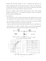
use a chart such as the one shown in Figure 5-8.
Figure 5-8. Conjugate mismatch loss chart.
The maximum power transfer takes place when the load impedance is equal to the complex
conjugate of the source impedance. For example, a source with 50 + j25 ohm impedance
delivers the maximum power to the load when the load impedance is 50 - j25ohm.
When the load impedance is not the conjugate of the source impedance, the conjugate
mismatch loss = the available power of source/power delivered to the load.
The above relationship can be expressed in terms of the reflection coefficient.
mismatch loss =
where ρ s = the reflection coefficient of the source.
ρ L = the reflection coefficient of the load.
Although ρ s and ρ L are not directly known in most cases, the above equation is still useful in
determining the maximum and the minimum mismatch power losses.
A. Maximum mismatch loss : This happens when the argument of ρ s plus the argument of ρ L
is equal to 180 degrees.
Then, the maximum mismatch =
Where SWRs = SWR at the source
SWRL = SWR at the load.
B. Minimum mismatch loss : This happens when the argument of ρ s plus the argument of ρ L
is equal to zero degrees.
Then, the minimum mismatch =
41
Example: For SWRs = 1.5 and SWRL = 1.25,
Calculate the maximum and the minimum mismatch loss.
Maximum mismatch loss =
Minimum mismatch loss =
42
Experiment 6:Standing Wave Measurement
1. Objectives.
Learn how to measure SWRx using slotted line or SWll indicator.
2. Theory.
At any point along a transmission line, we can think of the electromagnetic field as a sum of
two waveforms:
one is traveling toward the load (incident) and the other is traveling toward the generato
(reflected). The reason for the reflection is, as was already discussed in the previous chapter,
due to the impedance mismatch. Any open spot on the line is considered to be an impedance
mismatch and becomes a cause of the reflection as well. The amplitude and the phase of the
reflected wave depend upon the load impedance. The degree of the attenuation of the line
affects the amplitude of the reflected wave also. The only way the reflection can be
eliminated is either the line is infinitely long or there is impedance match between the load and
the transmission line. A standing wave results from the two traveling waves in opposite
direction. As was discussed in the previous chapter, the vector sum of the two waves create
minimum and maximum points on the standing wave pattern. Typical standing wave patterns in
a lossless transmission line are shown in Figure 6-1.
Fig. 6-1. Standing wave patterns in a lossless line.
In Figure 6-2, a voltage standing waveform in a transmission line having a characteristic
impedance of Zo and a load impedance of ZL is shown.
Fig, 6-2. A voltage standing waveform.
In Figure 6-2, the complex reflection coefficient is
43
Er
=
Ei
ρ=
Z
Z
-Zo
+Zo
…..(6-1)
Where Er = reflected signal ;
Ei = incident signal;
- = complex impedance at a given point.
Z
The evaluated at the load is:
ρL
=
…..(6-2)
ZL-Zo
ZL+Zo
Then,
Emax
VSWR
= S
=
Emin
|Ei|+|Er|
|Ei|-|Er
….(6-3)
Therefore,
|ρ|
=
S-1
…..(6-4)
S+1
3. Experiment procedure.
(1) Set up equipment as shown in Figure 6-3.
Fig. 6-3.
Setup diagram for SWR measurement.
(2) Set the Gunn diode supply voltage to +9V. Do not exceed this value.
(3) Set the variable attenuator to l0dB.
(4) Set the SWR indicator range switch to 20~40dB. Turn on the indicator.
(5) Turn on the Gunn oscillator.
(6) Apply the modulation signal to the PIN diode modulator.
(7) Adjust the SWR indicator frequency for the maximum meter deflection.
A. Measuring low and medium range SWR.
(1) Move the probe of the slotted line and observe the SWR indicator meter deflection.
(2) Completely disengage the probe of the slide screw tuner. At this point, the VSWR
indication should be very small (less than 1.3).Therefore, use the expanded scale for better
reading.
(3) Move the probe in the slotted line untill a maximum deflection is observed on the SWR
indicator. Adjust the gain of the SWR indicator untill the expanded meter reading reaches
1.0 . Both the coarse and the fine gain adjust are needed in the expanded scale.
(4) Move the probe to where a minimum deflection is observed. Take the reading on the
expanded scale and record it in Table 6-1
(5) Repeat the above procedure with three different probe depths. The three different depths are
required to be greater than the depth used in the above procedure. Fill in the Table 6-1
44
Table 6-1. Probe depth vs. VSWR,
Probe
depth(mm)
VSWR
B. Measuring high range SWR.
(1) Maximize the depth of the probe of the slide screw tuner. Large depth of probe is necessary
for high SWR measurements.
(2) Move the probe along the slotted line untill a minimum is observed on the indicator.
(3) Adjust the gain of the indicator untill 3Db is shown on the Db scale. If necessary, reduce the
attenuation of the variable attenuator.
(4) Move the probe along the slotted line untill 0dB (full scale) is obtained on the dB scale.
Table 6-2. Recording the 3dB measurement.
(5)Record the position of the probe under the d! Column in Table 6-2.
d1
d2
1st min
2nd min
λg
SWR
Probe penetration
[mm]
[mm]
[mm]
[mm]
[mm]
(6)Repeat the above procedure while moving the probe toward the right and record the position
of the probe under the d2 column.
Repeat the measurement at three different probe depths.
(7) Replace the slide screw tuner with a shorting plate. Find the distance between two adjacent
minimums. The guide wavelength As is twice of the distance.
(8) Compute the SWR using the following formula.
…..(6-5)
C. Measuring high SWR using a calibrated attenuator.
(1) Maximize the probe depth of the slide screw tuner.
(2) Move the porbe along the slotted line untill a minimum is observed.
(3) Set the variable attenuator to 10dB. (call this value AI). Adjust the gain of the SWR indicator
untill 3dB deviation is observed.
(4) Move the probe along the slotted line and adjust the attenuator untill the same maximum
value as in the previous step. Read the dB value (call this value A2) and record it in Table
6-3.
Table6-3. SWR measurement using a calibrated attenuator.
Probe penetration
A1 [dB] A2 [dB] SWR
(5) Calculate the SWR using the following formular and fill in the Table 6-3.
…(6-6)
Repeat the procedure at the different probe depths.
45
Experiment7:Impedance Measurement.
1. Objectives :
Learn the Smith chart and its application in determining unknown impedances.
2. Theory:
In a transmission line with the characteristic impedance of Zo, the reflection coefficient
between the incident and the reflected signal is defined as ;
……(7-1)
where Z = R + jX = load impedance connected to the line:
ρ =| ρ |ejθ=complex reflection coefficient.
The magnitude of the ρ (| ρ |) is the ratio of the amplitude between the incident and the
reflected signal. The angle θ represents the angle of rotation of the phase at the point of
reflection.
The voltage at any given point on a transmission line is the vector sum of the incident and the
reflected voltage waveforms. The resultant voltage waveforms are called the standing wave
pattern. In fact, when the two waveforms add phase, it forms a peak at that point.
Likewise. when the two waveforms add out of phase, a valley or a minimum voltage is
observed at that point.The voltage standing wave ratio. VSWR is defined as.
…..(7-2)
The angle of rotation of the phase of the reflection coefficient at a distance of “d” from the load
is determined by :
θ=2πd/λg
…..(7-3)
The determination of the load impedance can be a three step process :
1) Obtain data on the waveguide through well defined measurements.
2) Determine the magnitude and the phase of the reflection coefficient.
3) Calculate the load impedance.
The smith chart is used for the third process of determining the load impedance at any given
point on the waveguide (or a transmission line in general) from known reflection coefficients.
The Smith chart is a graphical representation of the impedance transformation property of a
length of transmission line. The chart coordinates give the normalized resistance and reactance.
They are normalized to Zo. The characteristic impedance of the waveguide. The VSWR circles
are usually not included but can be constructed as needed with a compass centered on the center
point of the chart. Notice that the distance scale on the outside periphery is normalized to the
guide wavelength. Usually. the best way to learn the Smith chart is to try to solve actual
problems. Let's take a look at a sample problem.
example: A waveguide is attached to a normalized load impedance of
0.6 + j1.2. The guide wavelength Ai is 42 millimeters.
a. Find the impedance 10mm from the load (See Figure 7-1).
b. Find the distance from the load where the first minimum of VSWR occurs.
Solution:
46
a. Refer to the Smith chart shown in Figure 7-2.
(1) Locate point A on the chart representing the load impedance of 0.6 + j1.2.
Fig.7-1 Sample problem for the Smith chart.
(2) Draw a straight line from 0 to A. This line intersects the distance circle (outer most
circle) at 0.15A toward generator. Traveling 10mm from the load is same as
traveling l0mm/42mm = 0.238A from the load.
(3) Locate a point on the distance circle which is equal to 0.15A + 0.238A = 0.388A.
Draw a straight line from the point to 0.
(4) Draw a circle with radius 0A centered at 0. The impedance at point B represents the
impedance of a point 10mm away from the load toward the generator. The
normalized impedance of point B is 0.38-j0.78.
b. The VSWR of 4.3 at point C is where the maximum of the VSWR pattern occurs. The
first minimum occurs at point D. The distance between point A and point D is
0.5A-0.15A = 0.35A .
Fig. 7-2. Solving the example using the Smith chart.
When working on a determination of unknown impedance, it is necessary to establish a
reference plane which the impedance can be related to. For example, the input terminals
of the unknown impedance can be a reference plane.
Once the reference plane is established, the unknown impedance can be measured ;
a. Connect the unknown impedance to a slotted line, then measure the VSWR and the
position of minimum value.
47
b. Replace the unknown with a short at the output of the slotted line, then measure the
distance between two adjacent minimum values. The distance obtained should be equal
to 0.5A of the guide wavelength.
c. Choose one of the minimum points as a reference (See Fig. 7-3).
Fig. 7-3. Fundamentals of impedance measurement.
Draw a VSWR circle on the Smith chart (See Figure 7-4). The impedance at the voltage
minimum is 1/SWR. When a short is placed across the load, the minimum of the VSWR
moves toward the load (See Figure 7-3). Therefore, the impedance at the load is
determined by drawing a straight line from a point d/A= away from the zero of the outer
most circle to the center of the VSWR circle. The intersection of the circle and the
straight line represents the load impedance.
Fig.7-4. Finding the load impedance using the Smith chart.
Notice that the line impedance equals the load impedance at A s/2,Ai, 3Aj/2 from the
load. So far, the analysis assumed that the waveguide was lossless. In case the waveguide
is lossy, any traces on the Smith chart becomes a spiral rather then a circle. In a lossy line,
the SWR increases when the point of observation moves toward the load and decreases
toward the generator.
48
3. Experiment procedure
A. Basic measurement.
(1) Set up equipment as shown in Figure 7-5.
(2) Completely unscrew the probe.
(3) Turn on the Gunn oscillator.
(4) Aply lkHz modulation signal to the PIN diode modulator.
(5) Measure the maximum and minimum value on the SWR indicator. Also Measure the
frequency of the oscillator.
Fig. 7-5.
Setup diagram of impedance measurement.
B. Impedance measurement.
(1) Observe the SWR indicator deflection at the 40dB range. Take the reading.
(2) Bring the probe of the slide screw tuner into the device such that the depth of probe is
approximately 5mm.
(3) Move the probe along the slotted line untill a maximum deflection is observed on the SWR
indicator.
(4)Adjust the SWR indicator untill the meter indicates 1.0.
(5) Move the probe along the slotted line until minimum deflection is observed. Record the
SWR value {SL) and the depth of the probe (dL)in Table 7-1
Table7-1 Data recording table for the impedance measurement.
Load
Load
Load
Short
λg
(dL-ds2)
Probe
λg
Impedance
Min
Minima
=2(ds1-ds2)
Penetration SWR
(mm)
see note
dL(mm) dL1(mm)
(mm)
ds2(mm)
frequency:
GHz
Note : In the following measurements, in case (dL – ds1} turns out to be positive, move the
probe toward the generator. If the value is negative move it toward the load. Also, note that
| D -D |
is always less than 0.25.
λ
(6) Remove the slide screw tuner and the matched termination from the setup. Place a shorting
plate to the slotted line.
(7) Obtain the distance ds! and ds2 which correspond to two adjacent minimum VSWRs. The
guide wavelengthλg is 2x(ds1-ds2).
Note : When measuring the minimum, it may be helpful to increase the gain of the SWR
indicator to obtain better accuracy.
(8) Repeat the procedure for two more different probe depths.
L
s1
g
49
Experiment 8:Basic Properties Of A Directional Coupler
1. ObJective:
Learn the basic properties of a directional coupler including the coupling coefficient and the
directivity.
2. Theory:
Directional coupler, as shown in Figure 8-I, is basically a sampling device of microwave
signal. The importance of the directional coupler as a sampling device is that it does not
introduce reflections to the main system. The physical structure of a directional coupler can
be thought of as a transmission line with one input port but two output ports. The directivity of
the directional coupler allows energy coupling in one direction only.
Fig. 8-i.
Directional coupler.
The basic properties of the directional coupler is graphically presented in Fig. 8-2 and Fig. 8-3.
Notice that one end of the directional coupler contains a matched termination.
(a) forward wave
(b) reflected wave.
Fig. 8-2.
Sampling direction of a directional coupler
The coupling coefficient and the directivity, which are the most important figure of merit of a
directional coupler, are defined as the following:
(dB)
……(8-1)
coupling coefficient = 10log PP
P
directivity =10log P (dB)
……(8-2)
1
3F
3F
3R
Fig. 8-3.
Return loss measurement.
When measuring return loss of a device, the input signal is applied at port2, and the device
under test(DUT) is connected to portl. Then the return signal is picked up at port3 (See Figure
8-3). The power at the detector when the coupling coefficient is C (or 10LogC dB) ;
P3 = PC
…..(8-3)
r
50
Since the voltage reflection coefficient of the DUT is given by
PI should be
known to make use of the expression. If the DUT is replaced by a short, all the input power is
reflected back and therefore, PI should appear at port3. The actual power at port3 is qual to P1 / C.
The ratio of the two signals detected at port3 is
(P1 / C) × (C / Pr)= 1 / |ρ |2
……(8-4)
The ratio as expressed in (8-4) is called return loss. The accuracy of he return loss measurement
is dependent upon the directivity of the oupler which describes how much of the input power at
port2 leaks into ort3. For example, a directivity of 40dB corresponds to a return loss of 40dB,
which,
in terms of reflection coefficient,
is
=0.01,The SWR in this case is
1+0.01
1-0.01
SWR=
=1.02
3. Experiment procedure.
A. Coupling factor measurment.
(1) Set up equipment as shown in Figure 8-4. Set the varible attenuator to 20dB. Apply
1000pps modulation signal to PIN diode modulator and turn on the Gunn oscillator. Read the
SWR indicator. Use this value
as a reference. Fill in Table 8-1 A1 with the value.
(20dB)
Fig. 8-4. Initial setup for coupling factor measurement.
(2) Replace the frequency meter with a directional coupler (Fig. 8-5). Move the crystal detector
to the auxiliary arm of the coupler.
Table 8-I. Data for coupling factor calculation
A1
A2
A3
A1-A2
A4
A3-A4
[dB]
[dB]
[dB]
+n×10
[dB] [dB]
[dB]
(3) Adjust the variable attenuator untill the same reference reading as in (1) is obtained.
(4) Fill in Table 8-1 A2 with the attenuation of the attenuator. The oupling factor of the
directional coupler is AI - A2.
51
Fig. 8-5. Setup diagram for coupling factor measurement.
B. Directivity measurement.
(1) Set the attenuator to 20dB.
(2) Read the SWR indicator. Use this value as a reference. Record the ttenuator setting (20dB)
in Table 8-1 A3.
(3) Change the coupler's orientation as specified in Fig. 8-6.
Fig. 8-6. Setup diagram for directivity measurement.
(4) Reduce the attenuation and increase the SWR indicator gain by l0dB or 20dB. (in l0dB
steps) untill the same value as in (2) is obtained. Fill in Table 8-1 A4 with the attenuation
of the attenuator. The directivity is {A3 - A4 + n x l0)dB.
C. Return loss measurement of a load.
Fig.8-7. Setup diagram for return loss measurement.
(1) Set up equipment as shown in Figure 8-7.
(2) Set the probe depth of the slide screw tuner to 5mm.
52
(3) Set the attenuator to 0Db (A5). Read the SWR indicator. Use this as a reference.
(4) Change the attenuator to maximum attenuation. Replace the load with a short.
(5) Decrease the attenuation untill the reference level in (3) is obtained. Record the attenuator
position (As). In case it is necessary to change the range on the SWR indicator, add the
increased value to the position of the attenuator to get A6.
(6) The return loss = (A6 - AS + n x10)dB
Table 8-2. Data for return loss calculation.
A6
(A5 -A6)+n×10)
A5
SWR
|-ρ |
[dB]
[dB]
[dB]
53
Experiment 9:Attenuation Measurement
1. Objective.
- Learn attenuation measurement techniques of microwave components.
2. Theory.
Although, attenuation in general means reduction or decrease of something, it specifically
refers to the ratio between the input to the output power in microwave.
P
…..(9-1)
A(dB)=10log P2
where P1 is the input power and P2 is the output power.
Insertion loss, although it has mathematically the same expression as (9-1), has completely
different meaning, While attenuation is introduced in the system on purpose, insertion loss is
an undesirable situation. The insertion loss is happening due to non-ideal physical components
in the system.In microwave waveguides, two different measurement methods are popular :
power ratio or RF substitution.
A. Power ratio method.
The power ratio method is simply taking the power measurement with and that the microwave
detector operates at different power level in each case, causing errors due to the non-llnearity
of the device. Therefore,
the measurement results need to be compensated. For
example, when the Output power of the detector diode is maintained at less then I milliwatt
level, about O. 3dB compensation is necessary for up to 20dB attenuation.
B. RF substitution method.
The error associated with the detector in the above method is eliminated in the RF substitution
method by first measuring the output power with the DUT then replacing the DUT with a
calibrated variable attenuator. By properly adjusting the variable attenuator to the same power
level as before attenuation of the DUT then, is simply the amount of attenuation of the
variable attenuator. So far, in both methods, we are based on the assumption that the errors
due to the impedance mismatch is insignificant. Sometimes. the SWR indicator itself
introduces e small amount of errors.
The AT3000 components are designed with less than±0.4dB of error rate.
3. Experiment Procedure.
A. Preliminary adjustment.
(1) Set up equipment as shown in Figure 9-1
1
Fig. 9-1 Setup for preliminary adjustment
(2) Turn the power supply on.
(3) Apply 1000pps modulation signal to the PIN diode.
(4)Adjust either the pulse repetition rate or the frequency on the SWR indicator for the
maximum deflection on the SWR indicator.
B. Measurement using the power ratio method.
(1) Set the variable attenuator to 20dB.
54
(2) Set the SWR indicator gain to either 30dB or 40dB range and adjust the indicator for 0dB.
(3) Using a directional coupler, add a matched termination to the setup as shown in Figure
9-2.
(4) Obtain the reading of the SWR indicator. Calculate the actual coupling of the directional
coupler.
(5) Repeat step (2),(3) and (4) with the attenuator set at 15 and 10dB respectively.
(6)Repeat the above experiment using fixed attenuators.
Figure 9-2. measuring attenuation using the power ratio method
C. Measurement using RF substitution method.
(1) Connect the crystal detector to the PIN diode modulator.(See Figure 9-1).
(2) Set the variable attenuator to 20dB. Adjust the SWR indicator's range switch and gain
control so that the indicator can indicate 0dB.
(3) Insert the directional coupler and connect the crystal detector to the auxiliary
arm of the directional coupler (See Figure 9-2). Without altering the SWR
indicator setting, adjust the variable attenuator untill the SWR indication is the same as
before. Record the attenuator setting. This is the actual value of the attenuation of the
directional coupler in this case.
(4) Repeat the above experiment using a fixed attenuator as a DUT.
D. Measurement of low values of attenuation.
(1) Set up equipment as shown in Figure 9-3.
Figure 9-3. setup diagram for the measurement of low values of attenuation
(2) Set the variable attenuator to 20dB.
(3) Measure the input SWR of the device under test (a directional coupler in this case).
(4)Deter=ine the attenuation using the following expression.
A=10log SWR+1
……(9-2)
SWR-1
55
Experiment 10:Study Of A Waveguide Hybrid - Tee
1. ObJectives:
- Understand the basic principle of Hybrid-T.
- Learn measurement methods on Hybrid-T characteristics.
2. Theory:
A hybrid-T or a magic-T of Figure 10-1 is basically a microwave version of a hybrid coil of the
type commonly used in telephone repeater circuits (See Figure 10-2).
Fig. 10-1 Waveguide Hybrid-T
Fig. 10-2. Balanced bridge circuit.
When the bridge circuit is properly matched by external impedances, the input signal applied at
portl appears at port2 and port3, but no signal appears at port4. In the same manner, when the
input is applied at port4, then the signal appears at port2 and port3 but no signal appears at portl.
The above input to output relationship can be described in terms of the field distribution inside of
the hybrid-T. A view of the electric field, with the input applied at portl, is shown in Figure
10-3(a). It's assumed that all arms of the hybrid-T are properly matched.
Fig.10-3(a). Electric field with input applied at portl.
The field, as shown in Fig. 10-3(a), is an even symmetry about the mid-plane. If the input signal
is applied at port4, the signal splits equally to port2 and port3 but no part of the signal enters
56
portl.
Fig. 10-3(b). Electric field with input applied at port4.
In Figure10-3(b). A sideview at the junction of the hybrid-T is shown when the input signal is
applied at port4 in TEl0 mode. The reason for no coupling to port1 is duo to reciprocity and the
symmetry of electric and magnetic field. The signal divides equal ly to port2 and port3 but the
phase is 180 degree out of phase. Arml is sometines refered to as H-arm because it is in the plane
of the magnetic field. Arm4 is refered to as E-arm for the similar reason. Another place where the
inputs can be applied to arm2 and arm3 at the same time. In this case. the vector sum of the
two inputs will appear at arm1. At am4, the vector difference of the two inputs will appear.
3. Experiment procedure.
A. Initial adjustnents.
Fig. 10-4. Initial setup diagram.
(1) Set up equipment as shown in Figure 10-4.
(2) Adjust the SWR indicator gain. for obtaining any convenient deflection.
(3) Apply 9V to the Gunn oscillator.
(4) Apply modulation voltage to the FIN diode modulator.
Adjust the offset voltage and the pulse frequency of the square wave generator to obtain the
maximum deflection on the SWR indicator.
B. Measurement of decoupling between H-arm and E-arm.
(1) Set the equipment as shown in Figure 10-5.
(2) Set the attenuator to 20dB. (AI).
(3) Select a range on the SWR indicator which gives a reasonable deflection on the indicator.
Adjust the gain control to a reference reading on the dB-scale of the indicator.
(4)Remove the detector and connect the variable attenuator to arml.
(5) Connect matched terminations and power meters to arm2 and arm3 and connect the
detector to arm4. Keep the power meter at off position.
(6) Increase the sensitivity of the SWR indicator in lOdB increment untill the same reference as
in (3) is obtained. The attenuation (Az) of the attenuator maybe reduced if necessary.
57
(7) Record the results to Table 10-1
Fig. 10-5. Setup diagram for measurement of decoupling between H arm and E arm.
Table 10-1. Decoupling between arm1 and arm4.
ATTENUATION OF
THE VARIABLE
ATTENUATIOR
A1
[dB]
VARIATIONS OF THE SWR
METER GAIN(in 10dB steps)
n steps
DECOUPLING
A1-A2+(n×10) [dB]
A2 [dB]
C. Measurement of insertion loss of hybrid-T (refer to Figure 10-4).
(1) Connect the detector to the attenuator which is set at 20dB.
(2) Select a range on the SWR indicator which gives a resonable deflec tion on the indicator.
Adjust the gain control to a reference reading on the dB-scale of the indicator.
(3) Remove the detector and connect the arm1 of the hybrid-T to the attenuator.
(4) Connect the matched terminations and the power meters to arm3 and arm4. Also connect
the detector to arm2.
(5) Decrease the attenuation(A4) untill the same reference level as in (2) is obtained. The
insertion loss between arm1 and arm2 is A3-A4.
(6) For insertion loss between arml and arm3, repeat (4) and (5).
(7) For insertion loss between arm4 and arm2, repeat (3),(4) and (5).
(8) Record the results in Table 10-2.
Table 10-2. Insertion loss of different path
信号通路臂
插入损
衰减值
耗
A3
[dB]
A4
[dB]
1-2
20
1-3
20
4-2
20
D. Return loss measurement of H-arm.
(1) Set up equipment as shown in Figure 10-6.
(2) Turn on the Gunn oscillator. Do not exceed 9V. Adjust the square wave output for the
maximum modulation.
(3) Set the variable attenuator to 20dB(As).
58
(4) Set up a reference point on the SWR indicator.
(5) Remove the shorting plate. Connect arml to the directional coupler as shown in Figure 10-7.
Connect a matched termination to arm3.Leave are4 open. (Arm4 is the E-plane T. Since
the decoupling to arm4 is almost 30-40dB. leaving it open should not affect th accuracy)
Fig. 10-6. Initial setup for return loss measurement.
(6) Increase the gain of the SWR indicator in 10dB increment. Decrease the attenuation(As)
untill the same level as in (4) is obtained.Record the results in Table 10-3.
(7) Repeat (5) and (6) using E-plane T (arm4) instead of H-plane T (arml).
Fig. 10-7. Return loss measurement setup.
Table 10-3. Return loss measurement data.
Object Attenuation
Gain increase of the Return loss
A5 dB
A6 dB SWR meter in 10dB dB
Absolute
steps
value
A6-A5+(n×10)
Arm1
Arm4
59
Smith Chart
Impedance or Admittance coordinates
60