1
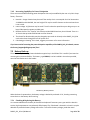
DNBFC_S12_PCIe REV2 Hardware Manual DNBFC_S12_PCIe H/W Manual Page 1 of 20 Copyright (c) 2011 Last Updated 2011-10-07 I. Yulaev Dini Group 7469 Draper Ave La Jolla, CA 92037 United States Phone: (858) 454-3419 Contact: Support: [email protected] Sales: [email protected] Web: http://www.dinigroup.com DNBFC_S12_PCIe H/W Manual Page 2 of 20 1 Table of Contents 1 Table of Contents .................................................................................................................................. 3 2 Introduction .......................................................................................................................................... 5 2.1 References .................................................................................................................................... 5 2.2 Terminology and Conventions ...................................................................................................... 5 2.3 Things Not To Do ........................................................................................................................... 5 2.4 Differences from Revision 1 .......................................................................................................... 5 3 Quick Start Guide .................................................................................................................................. 7 1. Setting up your Board ....................................................................................................................... 7 3.1 Power on and configuration ......................................................................................................... 7 3.2 Status LEDs .................................................................................................................................... 7 3.3 Loading the Driver & Running the Board ...................................................................................... 8 3.4 Re-Programming the pFPGA over JTAG ........................................................................................ 8 4 On-Board Interfaces ............................................................................................................................ 10 4.1 Block diagram.............................................................................................................................. 10 4.2 Chip-to-Chip Bus, “Horizontal” ................................................................................................... 10 4.3 Chip-to-Chip Bus, “Vertical” ........................................................................................................ 11 4.4 SF Bus .......................................................................................................................................... 11 4.5 DDR3 Discrete Chips ................................................................................................................... 12 4.6 FPGA ID ....................................................................................................................................... 12 5 Clocking ............................................................................................................................................... 13 1. 6 7 PROC Clock Network ....................................................................................................................... 13 5.1 PFPGASRC Clock Network ........................................................................................................... 13 5.2 MBCLK Clock Network................................................................................................................. 13 Off-Board Interfaces ........................................................................................................................... 14 6.1 PCI Express Interface................................................................................................................... 14 6.2 Daughter Card Interface ............................................................................................................. 14 6.3 JTAG ports ................................................................................................................................... 15 Power and Cooling .............................................................................................................................. 17 7.1 Power Connectors ....................................................................................................................... 17 7.2 Power Sequencing Requirements ............................................................................................... 17 DNBFC_S12_PCIe H/W Manual Page 3 of 20 7.3 Power Distribution ...................................................................................................................... 17 7.4 Power Dissipation ....................................................................................................................... 18 7.4.1 On-board Temperature Sensors ......................................................................................... 18 7.4.2 Increasing Capability for Power Dissipation ....................................................................... 19 7.5 Battery Back-up........................................................................................................................... 19 7.5.1 7.6 Checking & Replacing the Battery ....................................................................................... 19 Cleaning Heat-Sinks..................................................................................................................... 20 DNBFC_S12_PCIe H/W Manual Page 4 of 20 2 Introduction Congratulations on your purchase of a DNBFC_S12_PCIe Algorithm Acceleration board! This document attempts to address the typical questions and problems that a first-time user of a DNBFC_S12_PCIe might encounter. 2.1 References This document makes some reference to other pieces of documentation. These include: The board schematic. It is titled “503-0197-0000_02_customer.pdf” and should be found on your user CD. The board netlist. It is titled “503-0197-0000_02_customer.net” and should be found on your user CD. In many cases, these files capture more detail and are thus more useful than the H/W manual. These files will be referred to in many sections of this manual. 2.2 Terminology and Conventions There is a variety of board-specific terminology that will be used through this document. Much of it will be defined in context, but there are some general terms/names that are useful to know. gFPGA – describes the twelve FFG484-package Spartan-6 chips on this board. These are the “user FPGAs”, and are numbered F0 through F11. The block diagram in section 2 of this document displays the numbering convention for these FPGAs. dFPGA – this is the “dataflow manager” FPGA, the Spartan-6T FFG900 package with two daughter card headers and two DDR3 discrete chips. pFPGA – this is the “PCI Express” controller on this board. 2.3 Things Not To Do If you love your boards don't do the following: Don't move the power selection jumper while the board is plugged in and powered. Don't plug and unplug the board into live connectors, make sure your system/power supply is powered off before plugging and unplugging boards. 2.4 Differences from Revision 1 For users migrating from revision 1 DNBFC_S12_PCIe products, thank you continuing to use Dini Group solutions! For your convenience, a list of user-facing changes to the board is enumerated here. 1. PEG power connector replaces proprietary power header. 2. dFPGA trasitions to 900-pin package DNBFC_S12_PCIe H/W Manual Page 5 of 20 3. 4. 5. 6. 7. 100Ω external termination provided for the LVDS system clocks on Spartan-6 chips. EEPROM and temperature sensor I2C chain accessible from dFPGA now. Daughter card SelectIO signals move to dFPGA DDR3 CSn signal tied to GND with a 0Ω resistor CPLD, pFPGA, dFPGA, and gFPGA now share a single JTAG chain. Only one JTAG connector exists on the REV2 boards. These changes are discussed in further detail throughout this user manual. DNBFC_S12_PCIe H/W Manual Page 6 of 20 3 Quick Start Guide This section of the guide details how to bring up and begin playing with your DNBFC_S12_PCIe board. It is recommended that users unfamiliar with Dini Group products or FPGA boards in general follow the instructions, so as to familiarize oneself with the board and avoid common board bring-up mistakes. 1. Setting up your Board Skip this step if your board is already in a chassis. Before unwrapping the board, please put on a static grounding strap, to prevent ESD damage to the board. Plug the board into your host system. Make sure to find a minimum x4 PCI Express slot. Plug a +12V “PCI Express Graphics” power cable, coming directly from your ATX power supply, into the board’s power connector. If your power supply does not have a PCI Express Graphics connector, use the provided adapter to convert three hard drive power connectors into a single PEG header. Note that if your power supply does not come with PEG headers, it may have insufficient current on the +12V rail to power the DNBFC_S12_PCIe while running a high-power design. 3.1 Power on and configuration Power the system on. A green LED next to the power selection jumper should light if power is being delivered to the board. 3.2 Status LEDs If possible, check the status LEDs on the back-side of the board. Specifically, look at the row of 4 LEDs You should see the two LEDs furthest from the PCI Express fingers lit, and the two ones closer not lit. DNBFC_S12_PCIe H/W Manual Page 7 of 20 3.3 Loading the Driver & Running the Board A description of loading the driver and using the software with the board is outside of the scope of this manual. Please see the Software Manual, Chapter 2, for directions on performing these tasks. 3.4 Re-Programming the pFPGA over JTAG If the pFPGA PROM gets corrupted, for example, due to an error during firmware upgrade over PCIe, it may be necessary to re-program the PROM over JTAG. The board must be powered during this process. Note: Normally, programming the pFPGA PROM over JTAG is unnecessary. Updating a working firmware over PCI Express is the preferred way to perform a firmware upgrade. Only re-program the pFPGA PROM over JTAG if the firmware has been corrupted. Contact [email protected] if you are not 100% sure that this is the case. 1. Connect a Xilinx JTAG cable to the pFPGA JTAG header, circled below 2. Run Xilinx Impact. You should see the following screen, depicting the JTAG “chain” consisting of one device. DNBFC_S12_PCIe H/W Manual Page 8 of 20 3. Right-click on the part, and select “Add SPI/BPI flash.” Select the *.mcs file you want to program into the board, and hit OK. For the flash type, select “BPI PROM” and for part number use “XCF128X”. You should see the following image for the JTAG chain. 4. Now, right-click on the FLASH part and select “Program”. The programming takes a few minutes but should complete successfully. DNBFC_S12_PCIe H/W Manual Page 9 of 20 4 On-Board Interfaces This section details the on-board interfaces found on the DNBFC_S12_PCIe. These interfaces are used for moving data around on the board, as well as controlling your design. 4.1 Block diagram This is a high-level block diagram of the board. It will be referred to in this section. dFPGA F0 pFPGA F1 F5 F11 4.2 Chip-to-Chip Bus, “Horizontal” The horizontal chip-to-chip bus connects adjacent pairs of FPGAs. It is the dark-blue bus in the above diagram, connecting chips F0 to F1, F1 to F2, etc. The bus is 77-bits wide, allowing the user to implement a 64 or 72 bit interface and have a few pins left over as control signals. The pinout is the same between all “horizontal” busses, with the exception of the pins selected on the dFPGA. This means that, for example, net “FPGAHCC_F0F1_00” connects to pin U100.A13 and U101.AA1, therefore, “FPGAHCC_F1F2_00” will connect pins U101.A13 and U102.AA10, and so forth. The purpose of this convention is to allow the user to have a single design with the same pin mappings loaded into FPGAs F0 – F11. This bus is routed and timed to run at (at least) 90MHz “DDR”. This assumes source synchronous clocking in each direction. The clock signals are FPGAHCC_F<n>F<n+1>_CKp / FPGAHCC_F<n>F<n+1>_CKn in the “up” direction and FPGAHCC_F<n+1>F<n>_CKp / FPGAHCC_F<n+1>F<n>_CKn in the down direction. For example, DNBFC_S12_PCIe H/W Manual Page 10 of 20 FPGAHCC_F0F1_CKp/FPGAHCC_F0F1_CKn are used to clock signals going from FPGA F0 to FPGA F1, and FPGAHCC_F1F0_CKp/FPGAHCC_F1F0_CKn are used to clock signals going in the opposite direction. For the clock signals, make sure to use the signal standard “DIFF_HCSL_15”. See the reference design for exact syntax on how to declare these pins. The rest of the bus may be run with signal standard “LVCMOS15”. 4.3 Chip-to-Chip Bus, “Vertical” The horizontal chip-to-chip bus connects adjacent pairs of FPGAs. It is the dark-red bus in the above diagram, connecting chips F0 to F11, F1 to F10, etc. The bus is 89-bits wide, allowing the user to implement two 32 or 36-bit interfaces, or a single 64 or 72-bit interface, with plenty of pins to spare. There are also two differential clocks for source-synchronous clocking in each direction. The pinout is the same between all “vertical” busses. This means that, for example, net “FPGAVCC_F0F11_00” connects to pin U100.J19 and U111.U17, therefore, “FPGAVCC_F1F1-_00” will connect pins U101.J19 and U110.U17, and so forth. The purpose of this convention is to allow the user to have a single design with the same pin mappings loaded into FPGAs F0 – F11. Note that on the smaller Spartan-6 parts, some of the pins become no-connects. Therefore, the nets on these pins are no longer useable. On this board, all no-connect pins are connected together so that a minimum number of nets are lost. Pins with names starting with ‘x’ or ‘y’ are pins that become noconnects on LX100 and LX45 parts. Note that on LX45 parts, both ‘x’ and ‘y’ pins are lost. For customers using LX150 parts, no pins are lost. This bus is routed and timed to run at (at least) 90MHz “DDR”. This assumes source synchronous clocking in each direction. The clock signals are FPGAVCC_F<n>F<n+1>_CKp / FPGAVCC_F<n>F<n+1>_CKn in one direction and FPGAVCC_F<m>F<n>_CKp / FPGAVCC_F<n>F<m>_CKn in the other direction. For example, FPGAVCC_F0F11_CKp/FPGAVCC_F0F11_CKn are used to clock signals going from FPGA F0 to FPGA F11, and FPGAVCC_F11F0_CKp/FPGAVCC_F11F0_CKn are used to clock signals going in the opposite direction. For the clock signals, make sure to use the signal standard “DIFF_HCSL_15”. See the reference design for exact syntax on how to declare these pins. The rest of the bus may be run with signal standard “LVCMOS15”. The numbering for this bus assumes that the user will use ½ of the bus to communicate in one direction, and the other ½ to communicate in the other. This is why the convention is to number FPGAVCC_F<m>F<n>_[43:0] and FPGAVCC_F<n>F<m>_[44:0]. On the board level, the single-ended pins do not have any sort of implicit directionality. So you are free to use whatever pins you want for whatever direction you want. The bus may be treated as one bus of 89 pins, two busses of 44 pins, or however else is convenient to break it up. 4.4 SF Bus DNBFC_S12_PCIe H/W Manual Page 11 of 20 The SFB (Super-Fast Bus) is an 8-bit bus connecting the twelve gFPGAs to the pFPGA. The function of the pins is fixed based on the design loaded into the pFPGA. This bus is intended for communicating between PCI Express and the user FPGA in applications where a low-speed, low-latency interface is desirable. The bus pins are shared with the gFPGA SelectMAP configuration bus, thus, interleaving configuration and normal operation is difficult on the DNBFC_S12_PCIe, and it is recommended that all FPGAs be configured before the SFB is used. For a more detailed description of the timing, the exact pins used on each FPGA, and of the logical function of the SFB interface, please see the Software Manual for the DNBFC_S12_PCIe. 4.5 DDR3 Discrete Chips The DNBFC_S12_PCIe gives all FPGAs (except the pFPGA) dedicated DDR3 SDRAM memory for user application. The Spartan-6 chips have a DDR3 hardblock controller, so the user need not implement their own DDR3 design. Xilinx Coregen may be used to instantiate the hardblock for the user's design. The physical pinout on the chips is designed to be completely compatible with the Xilinx hardblock requirements. Clean routing and VTT supplies ensure that the DDR3 signals will have sufficient signal integrity to operate at 400MHz (800mbps per pin effective). Most of the DDR3 functionality is reference design related, and hence a full description of the interface is outside of the scope of the H/W manual. Please see the DNBFC_S12_PCIe Software Manual for more details on this interface. 4.6 FPGA ID FPGA ID pins are provided on all gFPGAs. The purpose is to allow the use of a single bitstream for all 12 user FPGAs; the chip ID pins allow each FPGA to determine what part it is on the board, in order to negotiate work transfers, SFB addresses, etc. Chip ID [3:0] pins are {H20, H19, H18, G19} respectively; they are pulled high or low. gFPGA 0 has chip ID 4’b000; gFPGA 11 has chip ID 4’b1011. DNBFC_S12_PCIe H/W Manual Page 12 of 20 5 Clocking There are three clock networks on the DNBFC_S12_PCIe. This section describes their function. 1. PROC Clock Network The PROC clock network is driven by and ICS84314-02 clock synthesizer, which can operate at speeds between 31.25MHz to 700MHz. Up to 350MHz, the clock frequency resolution is at least 1MHz. The synthesizer is programmed from the pFPGA, thus, the clock frequency must be set over PCI Express, i.e. through the Dini Group software provided with the board. This clock is distributed and length-matched to all FPGAs, and should be received with the LVDS signaling standard. On the gFPGAs, it connects to pins B10/A10 for the 'p' and 'n' nets respectively. On the dFPGA, it connects to pins W27 and W28. Please be sure to NOT use the DIFF_TERM attribute on the IBUFDS for each FPGA that uses this clock. External 100Ω termination is provided for these clock signals at the Spartan-6 FPGAs. 5.1 PFPGASRC Clock Network The PROC clock network is driven by the pFPGA, at a frequency of 125 MHz , and should be received with the LVDS signaling standard. The intention of this clock is to be used as the system synchronous clock for the "MainBus" interface, and also to be used as a frequency source for the DDR3 controller. In the latter case, this clock is multiplied up with a PLL to an appropriate frequency. This clock is "fixed frequency" and is derived from the PCI Express reference clock. Thus, if you are running the board without having PCI Express plugged in, this clock will not function. This clock is distributed and length-matched to all FPGAs. On the gFPGAs, it connects to pins AA12/AB12 for the 'p' and 'n' nets respectively. On the dFPGA, it connects to pins W29 and W30. Please be sure to NOT use the DIFF_TERM attribute on the IBUFDS for each FPGA that uses this clock. External 100Ω termination is provided for these clock signals at the Spartan-6 FPGAs. 5.2 MBCLK Clock Network The MBCLK clock network is driven by the pFPGA, at a frequency of 71.2MHz. This clock is "fixed frequency" and is derived from the PCI Express reference clock. Thus, if you are running the board without having PCI Express plugged in, this clock will not function. In the reference design, this clock has no fixed function. This clock is distributed and length-matched to all FPGAs, and should be received with the LVCMOS15 signaling standard. On the gFPGAs, it connects to pin C. On the dFPGA, it connects to pin AB28. DNBFC_S12_PCIe H/W Manual Page 13 of 20 6 Off-Board Interfaces There are several off-board interfaces on the DNBFC_S12_PCIe, with different purposes. The PCI Express interface is intended to move large amounts of data between the board and the host system. The daughter card interface is designed for moving a variable amount of data between boards, without having to go through the host system. The JTAG interfaces allow direct communication to the FPGAs, for configuration or debug. This section will discuss these off-board interfaces. The following picture shows the physical position of each of the interfaces. Board interfaces, color coded: daughter card headers, PCIe fingers, pFPGA JTAG, gFPGA + dFPGA JTAG 6.1 PCI Express Interface The PCI Express interface is the primary method of communication between the board and the host. The DNBFC_S12_PCIe implements a fully compliant 4-lane GEN2 PCI Express interface (backward-compatible with GEN1), and provides board-specific drivers and software. For more information on the PCI Express interface, please see the Software Manual for the DNBFC_S12_PCIe. 6.2 Daughter Card Interface The daughter card interface on the DNBFC_S12_PCIe comprises two Samtec EdgeRate connectors, mounted on the side of the board. Both connectors have identical pinout, and each has four lanes of high-speed serial (up to 3.125Gbps), 8 single ended signals, and +2.5V and +3.3V power. The intended purpose of this interface is either to host a daughter card or to connect to an adjacent DNBFC_S12_PCIe and transfer data between boards without host computer involvement. There is no clock on the daughter card interface. It is expected that both ends of each high-speed serial link have their own oscillator, and that the oscillator meets the ppm requirement for the protocol that the transceivers are using. For the single ended signals, it is expected that they are either used for a DNBFC_S12_PCIe H/W Manual Page 14 of 20 low-speed synchronous interface or an asynchronous interface. Clocking the single-ended signals is left to the user. The daughter card interface is designed so that a 1-2 cable (i.e. pins 1-2 are connected, pins 3-4 are connected etc.) can be used to link any pair of connectors. These cables can be acquired in arbitrary length from Samtec, furthermore, Dini Group keeps stock of commonly used lengths (connecting two adjacent PCIe hosted boards, or two boards far from each other in a chassis). Contact [email protected] for help with acquiring cables for your system. 6.3 JTAG ports There is a single JTAG port on the DNBFC_S12_PCIe. It can be used for firmware programming in the case that the on-board firmware is compromised. Also, it may be used to configure user FPGAs and perform debugging via utilities such as Xilinx ChipScope. In general, the JTAG interface is intended to be used for debugging purposes; its use as a general purpose board programming and communications interface is not supported. The JTAG ports may be interfaced to via a 14-pin Xilinx JTAG interface, using a cable such as Xilinx Platform Cable USB II. Links to distributorms may be found at the Xilinx Virtex Board Accessories page. Tools such as iMPACT may be used to scan the chain - they should output something like the following: DNBFC_S12_PCIe H/W Manual Page 15 of 20 The first device in the chain is the CPLD; this should never be programmed. The next device is the pFPGA. Following these two, the first device will be the dFPGA, and the rest will be the gFPGAs. If you have fewer than 12 gFPGA installed on your board, the chain will be shorter (uninstalled FPGAs will not appear). Using impact, you can manually program the gFPGAs one at a time (slow) or read back configuration information or debug status. Tools such as Xilinx Chipscope may aid the user in debugging his/her design inside the FPGA. DNBFC_S12_PCIe H/W Manual Page 16 of 20 7 Power and Cooling The DNBFC_S12_PCIe features dense logic which requires extensive power management. The board is capable of exceeding the PCI Express 25W limit even with a moderate design loaded. Thus, attention to the power distribution and dissipation limitations of the DNBFC_S12_PCIe is paramount to any user wishing to maintain a fast yet stable system 7.1 Power Connectors Since the DNBFC_S12_PCIe can dissipate well over 25W, an external “PCI Express Graphics” power connector is provided. This can be plugged into your power supply either directly or by means of an adapter. Powering the DNBFC_S12_PCIe from just the PCI Express fingers is not supported. PCIe fingers, circled in red +12V power connector, circled in orange 7.2 Power Sequencing Requirements When running a power-intensive design, bringing the entire design out of reset puts an extreme load step on the power supplies. Thus, it is advisable, for a high power design, to bring the FPGAs out of reset several at a time at 50ms intervals or longer, rather than bringing them all out of reset at once, especially if you are having problems with the board resetting as the parts come out of reset. A FPGA IDdependent timer inside the FPGA can be used to accomplish this. 7.3 Power Distribution The DNBFC_S12_PCIe has several high-power voltage rails used for internal FPGA logic and I/O power. The relevant ones to the user are: +VCCINT - VCCINT power for FPGAs F0-F3, F7-F11. 36W max. +VCCINT_2 - VCCINT power for FPGAs F4-F6. 12W max. DNBFC_S12_PCIe H/W Manual Page 17 of 20 +VCCINT_D - VCCINT power for dFPGA. 7.2W max. +1.5V - VCCIO power for all FPGAs. 45W max. The most likely limitation users will face will be VCCINT. If you are running an "aggressive" design or are experiencing voltage droop or spontaneous FPGA deconfiguration, try running your design through the XPE (Xilinx Power Estimator) spreadsheet. Make sure that your VCCINT and VCCIO requirements can be met by the on-board power supplies, as outlines above. 7.4 Power Dissipation The flip-side of power distribution is power dissipation. All of the power that your design consumes is shed in the form of heat. Heat must be managed so as to stay within the operating temperature range on the Spartan-6 devices on the DNBFC_S12_PCIe. There are four primary variables to be concerned with that will affect the heat dissipation capability of the board. These are 1. 2. 3. 4. Part grade, industrial vs commercial Heatsink type and size (active vs. passive and height) Chassis and fan type, for determining effective LFM of the board Ambient Air temperature of the chassis In the "Trenton 4U" chassis that the DNBFC_S12_PCIe typically ships in, at 25C ambient temperature, with commercial grade parts, the FPGAs can dissipate 4W, the limit of the power supplies. Greater power dissipation from the stock configuration may be realized by 1. Using industrial grade parts. These have a recommended max operating temperature of 100C rathern an 85C. 2. Using larger/taller heatsinks. This violates the PCI Express physical specification but may allow you to develop better thermal resistance between the chips and the ambient air. 3. Switching to a chassis with higher airflow. Contact the factory for availability. 4. Moving to a colder environment. Alternately, set the AC to blow very cold air. Contact the factory ([email protected]) for help regarding cooling your FPGAs. 7.4.1 On-board Temperature Sensors There are four on-board temperature monitors on the DNBFC_S12_PCIe. These may be used for getting an idea of the temperatures on the board. Note, however, that these do not perfectly reflect the temperature of the Spartan-6 chip die. There is no on-chip temperature sensor for Spartan-6 devices. The sensors are connected to the PCI Express controller "T" FPGA. This FPGA will de-configure the board automatically when it reads 85C (if your board has "C" grade parts) or 100C (if your board has "I" grade parts). This is expected behavior. In a room temperature (20C) environment with at least 300LFM of airflow, this temperature ceiling will be difficult to hit. DNBFC_S12_PCIe H/W Manual Page 18 of 20 7.4.2 Increasing Capability for Power Dissipation There are some variables affecting power dissipation that may be modified by the user or by Dini Group factory. These are 1. Heatsink - a larger heatsink may be used if the nearby slot is not occupied. See Cool Innovations 3-1010XXP and 4-1010XXP, the max height 27.9 may be used if clearance to the next board over is not critical. 2. Lower-voltage -1L(I) devices may be used. This will reduce the speed that your design may run at but will dissipate less power per MHz-gate. 3. Different chassis. The "Trenton" 4U chassis provides 300LFM and may host 12 board. There is a 1U chassis that provides 700LFM and can host 4 boards. 4. The chassis fan directionality may be changed to put cooler air directly to the DNBFC_S12_PCIe cards rather than through the host PC system first. 5. Calculating pre-heating. This is hard, suggest you contact us for more information. If you have need of increasing the power dissipation capability of the DNBFC_S12_PCIe board, contact the factory ([email protected]) first! 7.5 Battery Back-up There is a battery for storing a batter-backed encryption key in the FPGAs. This is useful if you intend to use encryption-protected bitfiles. The battery, type BR2012, is to be installed in the socket provided, near the PCIe bracket and +12V header. Location of Battery Socket When the board is powered on, the battery voltage is backed by on-board +2.5V, thereby preventing excess drain on the battery while running. 7.5.1 Checking & Replacing the Battery It is recommended that the battery be checked and replaced if necessary every year with the board in service. High temperatures may adversely affect battery life, if the board is housed in a chassis it may be advisable to probe the battery voltage more often. To check the battery voltage, probe the metal DNBFC_S12_PCIe H/W Manual Page 19 of 20 battery case (+) using ground as a reference. The batteries start at +3.0V nominal; a voltage below +2.7V suggests the battery should be replaced. Note that lithium batteries exhibit non-linear relationship between voltage and charge - a battery that has only lost a few hundreds of milivolts may in fact be nearing the end of its lifespan. If you don't need to keep the encryption keys, then the battery may be replaced by remove the old batter and installing a new one, with the board powered off. If the keys in the FPGA must be kept, battery replacement should be performed as follows. Before removing the old battery, wire in a battery socket to TP1, and power this with a fresh +3.0V lithium cell (size doesn't matter). Remove the old BR2012 battery, and install a new one. The battery at TP1 will continue to power the +VBATT rail while the battery in the socket is replaced. 7.6 Cleaning Heat-Sinks The heat sinks should be cleaned to maintain optimal heat transfer characteristics. Depending on how dusty the environment, cleaning may be necessary anywhere from once every few years to every few months. To clean the heat sinks, power off your system, open up the board chassis, and examine the heat sinks. If there is significant dust build-up in the heat sinks, use compressed air to remove the dust. Compressed air can be bought at any electronics store, and is often advertised for just this purpose, removing dust. DNBFC_S12_PCIe H/W Manual Page 20 of 20