1
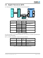
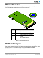
The Embedded I/O Company TPMC632 Reconfigurable FPGA with 64 TTL I/O / 32 Differential I/O Lines Version 1.0 User Manual Issue 1.0.4 September 2015 TEWS TECHNOLOGIES GmbH Am Bahnhof 7 25469 Halstenbek, Germany Phone: +49 (0) 4101 4058 0 Fax: +49 (0) 4101 4058 19 e-mail: [email protected] www.tews.com TPMC632-10R 64 TTL I/O Lines, XC6SLX45T-2 Spartan-6 FPGA,128 MB DDR3 This document contains information, which is proprietary to TEWS TECHNOLOGIES GmbH. Any reproduction without written permission is forbidden. TPMC632-11R 32 Differential I/O Lines, XC6SLX45T-2 Spartan6 FPGA,128 MB DDR3 TPMC632-12R 32 TTL and 16 Differential I/O Lines, XC6SLX45T-2 Spartan-6 FPGA,128 MB DDR3 TEWS TECHNOLOGIES GmbH has made any effort to ensure that this manual is accurate and complete. However TEWS TECHNOLOGIES GmbH reserves the right to change the product described in this document at any time without notice. TPMC632-13R TEWS TECHNOLOGIES GmbH is not liable for any damage arising out of the application or use of the device described herein. 32 Differential M-LVDS Lines, XC6SLX45T-2 Spartan-6 FPGA,128 MB DDR3 Style Conventions TPMC632-14R Hexadecimal characters are specified with prefix 0x, i.e. 0x029E (that means hexadecimal value 029E). 32 TTL and 16 Differential M-LVDS Lines, XC6SLX45T-2 Spartan-6 FPGA,128 MB DDR3 TPMC632-20R For signals on hardware products, an ‘Active Low’ is represented by the signal name with # following, i.e. IP_RESET#. 64 TTL I/O Lines, XC6SLX100T-2 Spartan-6 FPGA,128 MB DDR3 Access terms are described as: TPMC632-21R W Write Only R Read Only 32 Differential I/O Lines, XC6SLX100T-2 Spartan-6 FPGA,128 MB DDR3 R/W Read/Write R/C Read/Clear TPMC632-22R R/S Read/Set 32 TTL and 16 Differential I/O Lines, XC6SLX100T-2 Spartan-6 FPGA,128 MB DDR3 2015 by TEWS TECHNOLOGIES GmbH TPMC632-23R All trademarks mentioned are property of their respective owners. 32 Differential M-LVDS Lines, XC6SLX100T-2 Spartan-6 FPGA ,128 MB DDR3 TPMC632-24R 32 TTL and 16 Differential M-LVDS Lines, XC6SLX100T-2 Spartan-6 FPGA ,128 MB DDR3 TPMC632 User Manual Issue 1.0.4 Page 2 of 49 Issue Description Date 1.0.0 Initial Issue January 2012 1.0.1 Four further board variants with M-LVDS I/O buffers are created January 2013 1.0.2 Added chapter “Known Issue” May 2013 1.0.3 Added DDR3 SDRAM Alternative Part May 2015 1.0.4 Added SPI-Flash Alternative Part September 2015 TPMC632 User Manual Issue 1.0.4 Page 3 of 49 Table of Contents 1 2 3 PRODUCT DESCRIPTION ........................................................................................... 7 TECHNICAL SPECIFICATION ..................................................................................... 8 HANDLING AND OPERATION INSTRUCTION ......................................................... 10 3.1 3.2 4 ESD Protection .............................................................................................................................. 10 Thermal Considerations ............................................................................................................... 10 FUNCTIONAL DESCRIPTION .................................................................................... 11 4.1 FPGA Block Diagram .................................................................................................................... 11 4.2 FPGA .............................................................................................................................................. 12 4.3 Gigabit Transceiver (GTP) ............................................................................................................ 13 4.4 Configuration................................................................................................................................. 14 4.4.1 Selecting the Configuration Source ........................................................................................ 14 4.4.2 JTAG ....................................................................................................................................... 15 4.4.3 Board Configuration CPLD ..................................................................................................... 15 4.4.4 Programming Configuration devices....................................................................................... 16 4.5 Clocking ......................................................................................................................................... 17 4.5.1 FPGA Clock Sources .............................................................................................................. 17 4.6 I/O Interface ................................................................................................................................... 18 4.7 Memory .......................................................................................................................................... 22 4.7.1 DDR3 SDRAM ........................................................................................................................ 22 4.7.2 SPI-Flash ................................................................................................................................ 24 4.8 User GPIO ...................................................................................................................................... 25 4.9 On Board Indicators...................................................................................................................... 26 4.10 Thermal Management ................................................................................................................... 26 5 DESIGN HELP ............................................................................................................ 27 5.1 6 Example Design ............................................................................................................................ 27 INSTALLATION .......................................................................................................... 28 6.1 Pull Up Voltage .............................................................................................................................. 28 6.2 I/O Interface ................................................................................................................................... 29 6.2.1 TTL I/O Interface ..................................................................................................................... 29 6.2.2 Differential I/O Interface .......................................................................................................... 30 6.2.3 Multipoint-LVDS Interface ....................................................................................................... 30 6.3 Back I/O Configuration ................................................................................................................. 31 6.4 FPGA Debug Connector ............................................................................................................... 33 6.4.1 Connecting TA900 to TPMC632 Debug Connector ............................................................... 33 6.5 FPGA JTAG Connector ................................................................................................................ 34 7 PIN ASSIGNMENT – I/O CONNECTOR ..................................................................... 35 7.1 Overview ........................................................................................................................................ 35 7.2 X1 Front Panel I/O Connector ...................................................................................................... 35 7.2.1 Connector Type ...................................................................................................................... 35 7.2.2 Pin Assignment ....................................................................................................................... 36 7.3 Back I/O PMC Connector P14 ...................................................................................................... 37 7.3.1 Connector Type ...................................................................................................................... 37 7.3.2 Pin Assignment ....................................................................................................................... 37 7.4 X2 JTAG Header ............................................................................................................................ 39 7.4.1 Connector Type ...................................................................................................................... 39 7.4.2 Pin Assignment ....................................................................................................................... 39 TPMC632 User Manual Issue 1.0.4 Page 4 of 49 7.5 X3 Debug-Connector .................................................................................................................... 40 7.5.1 Connector Type ...................................................................................................................... 40 7.5.2 Pin Assignment ....................................................................................................................... 40 8 9 KNOWN ISSUES......................................................................................................... 41 APPENDIX A ............................................................................................................... 42 TPMC632 User Manual Issue 1.0.4 Page 5 of 49 List of Figures FIGURE 1-1 : BLOCK DIAGRAM ...................................................................................................................... 7 FIGURE 4-1 : FPGA BLOCK DIAGRAM ......................................................................................................... 11 FIGURE 4-2 : GTP BLOCK DIAGRAM ........................................................................................................... 13 FIGURE 4-3 : CONFIGURATION SOURCE SELECTION ............................................................................. 14 FIGURE 4-4 : CONFIGURATION DIP-SWITCH SETTINGS .......................................................................... 14 FIGURE 4-5 : JTAG-CHAIN ............................................................................................................................ 15 FIGURE 4-6 : CONFIGURATION DIP-SWITCH SETTINGS .......................................................................... 15 FIGURE 4-7 : FPGA CLOCK SOURCES ........................................................................................................ 17 FIGURE 6-1 : PULL (UP) VOLTAGE JUMPER SETTING.............................................................................. 28 FIGURE 6-2 : TTL I/O INTERFACE ................................................................................................................ 29 FIGURE 6-3 : DIFFERENTIAL I/O INTERFACE ............................................................................................. 30 FIGURE 6-4 : M-LVDS I/O INTERFACE ......................................................................................................... 30 FIGURE 6-5 : JUMPER POSITIONS FOR GROUND OPTION...................................................................... 31 FIGURE 6-6 : JUMPER POSITIONS FOR BACK I/O OPTIONS.................................................................... 32 FIGURE 6-7 : DEBUG CONNECTOR X3 ....................................................................................................... 33 FIGURE 6-8 : FPGA JTAG CONNECTOR X2 ................................................................................................ 34 FIGURE 7-1 : FRONT PANEL I/O CONNECTOR NUMBERING ................................................................... 35 List of Tables TABLE 2-1 : TECHNICAL SPECIFICATION ..................................................................................................... 9 TABLE 4-1 : TPMC632 FPGA FEATURE OVERVIEW .................................................................................. 12 TABLE 4-2 : FPGA BANK USAGE .................................................................................................................. 12 TABLE 4-3 : GTP CONNECTIONS ................................................................................................................. 13 TABLE 4-4 : MULTI GIGABIT TRANSCEIVER REFERENCE CLOCKS .......................................................13 TABLE 4-5 : AVAILABLE FPGA CLOCKS ...................................................................................................... 17 TABLE 4-6 : DIGITAL I/O INTERFACE ........................................................................................................... 21 TABLE 4-7 : DDR3 SDRAM INTERFACE....................................................................................................... 23 TABLE 4-8 : FPGA SPI-FLASH CONNECTIONS ........................................................................................... 24 TABLE 4-9 : FPGA GENERAL PURPOSE I/O ............................................................................................... 25 TABLE 4-10: BOARD-STATUS AND USER LEDS ........................................................................................ 26 TABLE 7-1 : PIN ASSIGNMENT FRONT PANEL I/O CONNECTOR X1 .......................................................36 TABLE 7-2 : PIN ASSIGNMENT BACK I/O PMC CONNECTOR P14 ...........................................................38 TABLE 7-3 : PIN ASSIGNMENT JTAG HEADER X2 ..................................................................................... 39 TABLE 7-4 : PIN ASSIGNMENT DEBUG CONNECTOR X3 ......................................................................... 40 TPMC632 User Manual Issue 1.0.4 Page 6 of 49 1 Product Description The TPMC632 is a standard single-width 32 bit PMC module providing a user configurable XC6SLX45T-2 or XC6SLX100T-2 Spartan-6 FPGA. The integrated Spartan-6’s PCIe Endpoint Block is connected to a PCIeto-PCI Bridge which routed to the PMC PCI Interface. Different variants of the TPMC632 provide ESD-protected TTL lines, ESD-protected differential I/O lines and differential Multipoint-LVDS lines. Also combination of 32 TTL and 16 differential I/O lines are supported. All lines are individually programmable as input, output or tri-state. The receivers are always enabled, which allows determining the state of each I/O line at any time. This can be used as read back function for lines configured as outputs. Each TTL I/O line has a pull resistor. The pull voltage level is selectable to be either +3.3V, +5V and additionally GND. The differential I/O lines are terminated by 120Ω resistors and the differential Multipoint-LVDS lines are terminated by 100Ω resistors. The FPGA is connected to a 128 Mbytes, 16 bit wide DDR3 SDRAM. As SDRAM-interface a hardwired internal Memory Controller Block of the Spartan-6 is used. The FPGA is configured by a platform flash or SPI flash. The flash device is in-system programmable. An incircuit debugging option is available via a JTAG header for read back and real-time debugging of the FPGA design (using Xilinx “ChipScope”). The TPMC632 provides either front panel I/O via a HD68 SCSI-3 type connector and rear panel I/O via P14. User applications for the TPMC632 with XC6SLX45T-2 FPGA can be developed using the design software ISE WebPACK which can be downloaded free of charge from www.xilinx.com. The larger FPGA densities require a full licensed ISE Design Suite. TEWS offers an FPGA Development Kit (TPMC632-FDK) which consists of well documented basic example design. It includes an .ucf file with all necessary pin assignments and basic timing constraints. The example design covers the main functionalities of the TPMC632. It implements a DMA capable PCIe endpoint with interrupt support, register mapping, DDR3 memory access and basic I/O. It comes as a Xilinx ISE project with source code and as a ready-to-download bitstream. Please note: The basic example design requires the Embedded Development Kit (EDK), which is part of the Embedded or System Edition of the ISE Design Suite from Xilinx (downloadable from www.xilinx.com, a 30 day evaluation license is available). Software Support (TPMC632-SW-xx) for different operating systems is available. Figure 1-1 : Block Diagram TPMC632 User Manual Issue 1.0.4 Page 7 of 49 2 Technical Specification PMC Interface Mechanical Interface PCI Mezzanine Card (PMC) Interface confirming to IEEE P1386/P1386.1 Single Size Electrical Interface PCI Rev. 3.0 compliant 33 MHz or 66 MHz / 32 bit PCI 3.3V and 5V PCI Signaling Voltage On Board Devices PCI to PCI Express Bridge PEX8112 (PLX Technology) PCI Express Endpoint Spartan-6 PCI Express Endpoint Block User configurable FPGA TPMC632-1xR: XC6SLX45T-2 (Xilinx) TPMC632-2xR: XC6SLX100T-2 (Xilinx) Configuration Flash TPMC632-1xR: XCF16P (Xilinx) TPMC632-2xR: XCF32P (Xilinx) SPI-Flash W25Q32 (Winbond) 32 Mbit (can be used for FPGA configuration) W25Q32 (Winbond) 32 Mbit (contains TPMC632 FPGA Example) DDR3 RAM MT41J64M16 or MT41K64M16 (Micron) 64 Meg x 16 Bit I/O Interface Number of Channels TPMC632-x0R: 64 ESD-protected TTL lines TPMC632-x1R: 32 differential I/O lines TPMC632-x2R: 32 TTL and 16 differential I/O lines TPMC632-x3R: 32 M-LVDS I/O lines TPMC632-x4R: 32 TTL and 16 M-LVDS I/O lines. TTL signaling voltage level (maximum current:+/-32 mA), EIA-422/-485 signaling level or M-LVDS Standard (TIA/EIA-899) I/O Connector Front I/O HD68 SCSI-3 type Connector (AMP 787082-7 or compatible) PMC P14 I/O (64 pin Mezzanine Connector) Physical Data Power Requirements TPMC632 User Manual Issue 1.0.4 Depends on FPGA design With TPMC632 FPGA Example Design / without external load typical @ +3.3V DC typical @ +5.0V DC Output disable enable disable drive low TPMC632-x0R 860mA 900mA <5mA 72mA TPMC632-x1R 860mA 1600mA <5mA <5mA TPMC632-x2R 860mA 1260mA <5mA 36mA TPMC632-x3R 640mA 640mA <5mA <5mA TPMC632-x4R 860mA 980mA <5mA 36mA Page 8 of 49 Temperature Range Operating Storage MTBF TPMC632-10R/-20R: 291000 h TPMC632-11R/-21R: 336000 h TPMC632-12R/-22R: 311000 h TPMC632-13R/-23R: 324000 h TPMC632-14R/-24R: 306000 h -40°C to +85°C -40°C to +85°C MTBF values shown are based on calculation according to MIL-HDBK-217F and MIL-HDBK-217F Notice 2; Environment: GB 20°C. The MTBF calculation is based on component FIT rates provided by the component suppliers. If FIT rates are not available, MIL-HDBK-217F and MIL-HDBK-217F Notice 2 formulas are used for FIT rate calculation. Humidity 5 – 95 % non-condensing Weight TPMC632-xxR: 126 g Table 2-1 : Technical Specification TPMC632 User Manual Issue 1.0.4 Page 9 of 49 3 Handling and Operation Instruction 3.1 ESD Protection The TPMC632 is sensitive to static electricity. Packing, unpacking and all other handling of the TPMC632 has to be done in an ESD/EOS protected Area. 3.2 Thermal Considerations Forced air cooling is recommended during operation. Without forced air cooling, damage to the device can occur. TPMC632 User Manual Issue 1.0.4 Page 10 of 49 4 Functional Description 4.1 FPGA Block Diagram PCIe to PCI Bridge GPIO: - DIP-Switch - LEDs - I2C - User LEDs - Debug Header GTP Bank 0 VCCO = 3.3V Bank 1 Spartan-6 VCCO = 1.5V - 64 x Output VCCO = 3.3V - 64 x Input Bank 3 Digital I/O - 64 x O. Enable DDR3 Bank VCCO = 3.3V Bank 2 SPI-Flash (User) Platform Flash SPI-Flash (Example Design) Config Figure 4-1 : FPGA Block Diagram TPMC632 User Manual Issue 1.0.4 Page 11 of 49 4.2 FPGA The FPGA is a Spartan-6 LX45T-2 or LX100T-2 FPGA. Each Spartan-6 FPGA in a FGG484 package provides two Memory Controller Blocks and one Endpoint Block for PCI Express (x1 Linkage). Spartan-6 Slices FlipFlops DSP48A1 Slices Block RAM (Kb) CMTs GTP Transceivers LX45T 6.822 54.576 58 2.088 4 4 LX100T 15.822 126.576 180 4.824 6 4 Table 4-1 : TPMC632 FPGA Feature Overview The board supports JTAG, master serial mode configuration from SPI-Flash or SelectMAP configuration from a Platform Flash. The FPGA is equipped with 4 I/O banks and 4 GTP transceivers. Bank VCCO VREF Signals Bank 0 3.3V none dig. I/O Interface Bank 1 1.5V 0.75V DDR3 Bank Bank 2 3.3V none dig. I/O Interface Bank 3 3.3V none dig. I/O Interface GTP Bank Description Remarks +GPIO / LED /Debug +Configuration Remarks GTP101 PCIe Endpoint Block Lane 0 GTP101 not used Lane 1 GTP123 not used Lane 0 GTP123 not used Lane 1 Table 4-2 : FPGA Bank Usage The FPGA’s VCCAUX is connected to the 3.3V supply. TPMC632 User Manual Issue 1.0.4 Page 12 of 49 4.3 Gigabit Transceiver (GTP) PCIe Clock 125 MHz 100 MHz GTP 123 CLK0 Bridge Clock GTP 123 CLK1 PCIe X1 Interface GTP 101 CLK1 Spartan-6 GTP 101 CLK0 PCI Interface PCIe to PCI Bridge PMC-Connector The TPMC632 provides one GTP as Spartan-6 PCI Express Endpoint Block. SI5338 Figure 4-2 : GTP Block Diagram GTP MGT0_101 MGT1_101 MGT0_123 MGT1_123 Signal FPGA Pins Connected to MGTTX B6 / A6 MGTRX D7 / C7 used for PCI Express Endpoint Block MGTTX B8 / A8 not used MGTRX D9 / C9 MGTTX B14 / A14 MGTRX D13 / C13 MGTTX B16 / A16 MGTRX D15 / C15 not used not used Table 4-3 : GTP Connections The GTP clock MGT0_101 (PCI Express Endpoint Block clock reference) of 125 MHz is generated by the SI5338 low-jitter clock generator. MGT1_101, MGT0_123 and MGT1_123 are not used on the TPMC632. GTP Signal FPGA Pins Connected to MGT0_101 MGTREFCLK A10 / B10 125 MHz (derived SI5338 clock generator) MGT1_101 MGTREFCLK C11 / D11 not used MGT0_123 MGTREFCLK A12 / B12 not used MGT1_123 MGTREFCLK E12 / F12 not used Table 4-4 : Multi Gigabit Transceiver Reference Clocks TPMC632 User Manual Issue 1.0.4 Page 13 of 49 4.4 Configuration The FPGA can be configured by the following sources: • Platform Flash • SPI-Flash • JTAG The configuration flash can be selected with a DIP-switch; alternatively, JTAG configuration is always available. For the XILINX Platform Flash configuration the Master SelectMAP/BPI mode with 8bit bus width is used. The SPI-Flash configuration uses the Master Serial / SPI mode. Both flashes could be programmed via JTAG; the SPI-Flash uses the indirect SPI programming mode. To change the TPMC632 programming, JTAG-capable hardware is needed (i.e. the Xilinx Platform Cable USB II). On delivery the configuration Platform Flash and the User SPI-Flash (USER Flash) are blank. A second SPI-Flash (TEWS Flash) is factory programmed with the TPMC632 Platform Example Application. 4.4.1 Selecting the Configuration Source Besides direct JTAG configuration, the TPMC632 provides two user configuration sources: a platform flash and a SPI-Flash. Both devices share common pins, so a selection must be made. With the Configuration DIP switch the Configuration source could be selected. Set the Configuration DIP Switch S1 to ON, the SPI Flash interface is selected, with Configuration DIP Switch S1 set to OFF the FPGA will configure from the Platform Flash. Set the Configuration DIP Switch S2 to ON the SPI Flash A (USER Flash) is selected. Set the Configuration DIP Switch S2 to OFF the SPI Flash B (TEWS Flash) is selected. MUX XCF MUX SPI A SPI B FPGA S1 S2 Figure 4-3 : Configuration Source Selection After configuration the SPI-Flash A is always user accessible, regardless of the switch setting. Switch Signal S1 ON Configure FPGA from SPI Flash OFF Configure FPGA from Platform Flash ON SPI Flash A (USER Flash) selected OFF SPI Flash B (TEWS Flash) selected S2 Description Figure 4-4 : Configuration DIP-Switch Settings TPMC632 User Manual Issue 1.0.4 Page 14 of 49 4.4.2 JTAG The JTAG-chain is accessible from the JTAG Header, from the Debug Connector or from the PMC-Interface. These interfaces are connected in parallel, so only one connection should be made to avoid signal contentions/possible hardware damage. X3 X2 Debug-Connector JTAG-Header XC6SLX...T XCF16/32 PEX8112 XC2C32 TDI TDO TDI TDO TDI TDO TDI TDO MUX J11/J12 PMC-Connector For direct FPGA configuration, FPGA readback or in-system diagnostics with ChipScope, the JTAG Header can be used to access the JTAG-chain. The JTAG-chain can be extended to include the TPMC632 configuration CPLD. S3 Figure 4-5 : JTAG-Chain S3 S4 ON Include configuration CPLD to JTAG chain. OFF Bypass configuration CPLD (default) ON Not used OFF Figure 4-6 : Configuration DIP-Switch Settings 4.4.3 Board Configuration CPLD The Board Configuration CPLD (BCC) is factory configured, and handles the basic board setup. Changing or erase the BCC content leads to an inoperable TPMC632 FPGA configuration. TPMC632 User Manual Issue 1.0.4 Page 15 of 49 4.4.4 Programming Configuration devices Both user configuration devices XILINX Platform Flash and SPI Flash could be programmed via JTAG interface. The second SPI Flash (TEWS Flash) could not be programmed. For programming the configuration devices the XILINX programming tool iMPACT can be used. An addition JTAG programming hardware is needed (i.e. the Xilinx Platform Cable USB II). To use the maximum configuration speed, the TPMC632 must be configured to use the 32 MHz external master clock as CCLK. To use these configuration feature, the configuration option ‘Enable External Master Clock’ (-g ExtMasterCclk_en) must be enabled. Without this option, the configuration time for the Spartan6 FPGA exceed the maximum PCI bus setup time. TPMC632-1xR configuration devices: SPI Flash: Winbond W25Q32BV or W25Q32FV; 32M; Data Width = 4bit XILINX Flash/PROM: XCF16P; 16M; parallel mode TPMC632-2xR configuration devices: SPI Flash: Winbond W25Q32BV or W25Q32FV; 32M; Data Width = 4bit XILINX Flash/PROM: XCF32P; 32M; parallel mode TPMC632 User Manual Issue 1.0.4 Page 16 of 49 4.5 Clocking 4.5.1 FPGA Clock Sources USER_CLK Si5338 32MHz Clock USER_CCLK 32MHz Clock Spartan-6 GTP 123 CLK0 GTP 123 CLK1 GTP 101 CLK1 PCIe Clock GTP 101 CLK0 MCB_CLK Figure 4-7 : FPGA Clock Sources The following table lists the available clock sources on the TPMC632: FPGA Clock-Pin Name MGTREFCLK0_101 FPGA Pin Number Source Description A10 / B10 SI5338 low-jitter clock generator 125 MHz PCIe Reference clock IO_L30P_GCLK1_D13_2 Y13 SI5338 low-jitter clock generator MCB CLK 62.5 MHz IO_L29N_GCLK2_2 U12 SI5338 low-jitter clock generator USER CLK 83.3325 MHz AB13 32MHz, 3,3V oscillator Used for external configuration clock (CCLK) After configuration this clock could be used by FPGA design. IO_L30N_GCLK0_USERCCLK_2 Table 4-5 : Available FPGA clocks TPMC632 User Manual Issue 1.0.4 Page 17 of 49 4.6 I/O Interface Each of the 64 digital IO channels are realized with single ended or differential digital buffers. Each channel provides an input; output and an output enable signal which is direct connected to the FPGA device. The IO channels are accessible through the IO Bank 0, Bank 2 and Bank 3 of the Spartan-6 FPGA. The subsequent table lists required I/O setting for correct interfacing. Signal Name FPGA_IN<0># FPGA_IN<1># FPGA_IN<2># FPGA_IN<3># FPGA_IN<4># FPGA_IN<5># FPGA_IN<6># FPGA_IN<7># FPGA_IN<8># FPGA_IN<9># FPGA_IN<10># FPGA_IN<11># FPGA_IN<12># FPGA_IN<13># FPGA_IN<14># FPGA_IN<15># FPGA_IN<16># FPGA_IN<17># FPGA_IN<18># FPGA_IN<19># FPGA_IN<20># FPGA_IN<21># FPGA_IN<22># FPGA_IN<23># FPGA_IN<24># FPGA_IN<25># FPGA_IN<26># FPGA_IN<27># FPGA_IN<28># FPGA_IN<29># FPGA_IN<30># FPGA_IN<31># FPGA_IN<32># FPGA_IN<33># FPGA_IN<34># FPGA_IN<35># FPGA_IN<36># FPGA_IN<37># FPGA_IN<38># FPGA_IN<39># Pin Number L4 M3 M4 M5 N4 P3 L1 L3 V17 W18 Y17 V15 W17 Y18 V2 Y1 Y14 Y15 B2 C3 A4 D4 H14 D5 E5 E6 A19 F16 A2 D3 B20 F8 H11 H10 G9 G8 B3 A3 A18 B18 TPMC632 User Manual Issue 1.0.4 Direction INPUT INPUT INPUT INPUT INPUT INPUT INPUT INPUT INPUT INPUT INPUT INPUT INPUT INPUT INPUT INPUT INPUT INPUT INPUT INPUT INPUT INPUT INPUT INPUT INPUT INPUT INPUT INPUT INPUT INPUT INPUT INPUT INPUT INPUT INPUT INPUT INPUT INPUT INPUT INPUT IO Standard LVCMOS33 LVCMOS33 LVCMOS33 LVCMOS33 LVCMOS33 LVCMOS33 LVCMOS33 LVCMOS33 LVCMOS33 LVCMOS33 LVCMOS33 LVCMOS33 LVCMOS33 LVCMOS33 LVCMOS33 LVCMOS33 LVCMOS33 LVCMOS33 LVCMOS33 LVCMOS33 LVCMOS33 LVCMOS33 LVCMOS33 LVCMOS33 LVCMOS33 LVCMOS33 LVCMOS33 LVCMOS33 LVCMOS33 LVCMOS33 LVCMOS33 LVCMOS33 LVCMOS33 LVCMOS33 LVCMOS33 LVCMOS33 LVCMOS33 LVCMOS33 LVCMOS33 LVCMOS33 IO Bank 3 3 3 3 3 3 3 3 2 2 2 2 2 2 3 3 2 2 0 0 0 0 0 0 0 0 0 0 0 0 0 0 0 0 0 0 0 0 0 0 Drive [mA] Slew Rate Page 18 of 49 FPGA_IN<40># FPGA_IN<41># FPGA_IN<42># FPGA_IN<43># FPGA_IN<44># FPGA_IN<45># FPGA_IN<46># FPGA_IN<47># FPGA_IN<48># FPGA_IN<49># FPGA_IN<50># FPGA_IN<51># FPGA_IN<52># FPGA_IN<53># FPGA_IN<54># FPGA_IN<55># FPGA_IN<56># FPGA_IN<57># FPGA_IN<58># FPGA_IN<59># FPGA_IN<60># FPGA_IN<61># FPGA_IN<62># FPGA_IN<63># FPGA_OE<0># FPGA_OE<1># FPGA_OE<2># FPGA_OE<3># FPGA_OE<4># FPGA_OE<5># FPGA_OE<6># FPGA_OE<7># FPGA_OE<8># FPGA_OE<9># FPGA_OE<10># FPGA_OE<11># FPGA_OE<12># FPGA_OE<13># FPGA_OE<14># FPGA_OE<15># FPGA_OE<16># FPGA_OE<17># FPGA_OE<18># FPGA_OE<19># FPGA_OE<20># FPGA_OE<21># FPGA_OE<22># FPGA_OE<23># FPGA_OE<24># FPGA_OE<25># FPGA_OE<26># A17 A5 C5 C4 G13 G15 D17 E16 G16 F17 D18 D19 F15 F9 C19 F7 G11 F14 C18 C17 A20 H12 F10 H13 T15 AB16 AB11 AB8 AB10 AB7 W8 AB9 R8 AB4 AB17 AB15 W12 R1 V1 T7 U6 AB19 C1 M8 AA18 AB18 U14 W14 Y16 U16 V13 TPMC632 User Manual Issue 1.0.4 INPUT INPUT INPUT INPUT INPUT INPUT INPUT INPUT INPUT INPUT INPUT INPUT INPUT INPUT INPUT INPUT INPUT INPUT INPUT INPUT INPUT INPUT INPUT INPUT OUTPUT OUTPUT OUTPUT OUTPUT OUTPUT OUTPUT OUTPUT OUTPUT OUTPUT OUTPUT OUTPUT OUTPUT OUTPUT OUTPUT OUTPUT OUTPUT OUTPUT OUTPUT OUTPUT OUTPUT OUTPUT OUTPUT OUTPUT OUTPUT OUTPUT OUTPUT OUTPUT LVCMOS33 LVCMOS33 LVCMOS33 LVCMOS33 LVCMOS33 LVCMOS33 LVCMOS33 LVCMOS33 LVCMOS33 LVCMOS33 LVCMOS33 LVCMOS33 LVCMOS33 LVCMOS33 LVCMOS33 LVCMOS33 LVCMOS33 LVCMOS33 LVCMOS33 LVCMOS33 LVCMOS33 LVCMOS33 LVCMOS33 LVCMOS33 LVCMOS33 LVCMOS33 LVCMOS33 LVCMOS33 LVCMOS33 LVCMOS33 LVCMOS33 LVCMOS33 LVCMOS33 LVCMOS33 LVCMOS33 LVCMOS33 LVCMOS33 LVCMOS33 LVCMOS33 LVCMOS33 LVCMOS33 LVCMOS33 LVCMOS33 LVCMOS33 LVCMOS33 LVCMOS33 LVCMOS33 LVCMOS33 LVCMOS33 LVCMOS33 LVCMOS33 0 0 0 0 0 0 0 0 0 0 0 0 0 0 0 0 0 0 0 0 0 0 0 0 2 2 2 2 2 2 2 2 2 2 2 2 2 3 3 2 2 2 3 3 2 2 2 2 2 2 2 8 8 8 8 8 8 8 8 8 8 8 8 8 8 8 8 8 8 8 8 8 8 8 8 8 8 8 SLOW SLOW SLOW SLOW SLOW SLOW SLOW SLOW SLOW SLOW SLOW SLOW SLOW SLOW SLOW SLOW SLOW SLOW SLOW SLOW SLOW SLOW SLOW SLOW SLOW SLOW SLOW Page 19 of 49 FPGA_OE<27># FPGA_OE<28># FPGA_OE<29># FPGA_OE<30># FPGA_OE<31># FPGA_OE<32># FPGA_OE<33># FPGA_OE<34># FPGA_OE<35># FPGA_OE<36># FPGA_OE<37># FPGA_OE<38># FPGA_OE<39># FPGA_OE<40># FPGA_OE<41># FPGA_OE<42># FPGA_OE<43># FPGA_OE<44># FPGA_OE<45># FPGA_OE<46># FPGA_OE<47># FPGA_OE<48># FPGA_OE<49># FPGA_OE<50># FPGA_OE<51># FPGA_OE<52># FPGA_OE<53># FPGA_OE<54># FPGA_OE<55># FPGA_OE<56># FPGA_OE<57># FPGA_OE<58># FPGA_OE<59># FPGA_OE<60># FPGA_OE<61># FPGA_OE<62># FPGA_OE<63># FPGA_OUT<0># FPGA_OUT<1># FPGA_OUT<2># FPGA_OUT<3># FPGA_OUT<4># FPGA_OUT<5># FPGA_OUT<6># FPGA_OUT<7># FPGA_OUT<8># FPGA_OUT<9># FPGA_OUT<10># FPGA_OUT<11># FPGA_OUT<12># FPGA_OUT<13># FPGA_OUT<14># W13 U1 AA1 U13 AA2 W6 W4 R3 T6 D1 V3 H5 J6 F2 G1 H2 H1 U3 U4 T3 P6 R7 M7 U8 M2 T4 V5 K1 N1 P5 N6 K2 N7 P7 P1 K5 J4 Y3 AB14 AB12 AA4 N3 W3 AA10 Y6 M6 L6 K4 K3 P2 T1 J3 TPMC632 User Manual Issue 1.0.4 OUTPUT OUTPUT OUTPUT OUTPUT OUTPUT OUTPUT OUTPUT OUTPUT OUTPUT OUTPUT OUTPUT OUTPUT OUTPUT OUTPUT OUTPUT OUTPUT OUTPUT OUTPUT OUTPUT OUTPUT OUTPUT OUTPUT OUTPUT OUTPUT OUTPUT OUTPUT OUTPUT OUTPUT OUTPUT OUTPUT OUTPUT OUTPUT OUTPUT OUTPUT OUTPUT OUTPUT OUTPUT OUTPUT OUTPUT OUTPUT OUTPUT OUTPUT OUTPUT OUTPUT OUTPUT OUTPUT OUTPUT OUTPUT OUTPUT OUTPUT OUTPUT OUTPUT LVCMOS33 LVCMOS33 LVCMOS33 LVCMOS33 LVCMOS33 LVCMOS33 LVCMOS33 LVCMOS33 LVCMOS33 LVCMOS33 LVCMOS33 LVCMOS33 LVCMOS33 LVCMOS33 LVCMOS33 LVCMOS33 LVCMOS33 LVCMOS33 LVCMOS33 LVCMOS33 LVCMOS33 LVCMOS33 LVCMOS33 LVCMOS33 LVCMOS33 LVCMOS33 LVCMOS33 LVCMOS33 LVCMOS33 LVCMOS33 LVCMOS33 LVCMOS33 LVCMOS33 LVCMOS33 LVCMOS33 LVCMOS33 LVCMOS33 LVCMOS33 LVCMOS33 LVCMOS33 LVCMOS33 LVCMOS33 LVCMOS33 LVCMOS33 LVCMOS33 LVCMOS33 LVCMOS33 LVCMOS33 LVCMOS33 LVCMOS33 LVCMOS33 LVCMOS33 2 3 3 2 3 2 3 3 3 3 3 3 3 3 3 3 3 3 3 3 3 3 3 2 3 3 3 3 3 3 3 3 3 3 3 3 3 3 2 2 2 3 3 2 2 3 3 3 3 3 3 3 8 8 8 8 8 8 8 8 8 8 8 8 8 8 8 8 8 8 8 8 8 8 8 8 8 8 8 8 8 8 8 8 8 8 8 8 8 8 8 8 8 8 8 8 8 8 8 8 8 8 8 8 SLOW SLOW SLOW SLOW SLOW SLOW SLOW SLOW SLOW SLOW SLOW SLOW SLOW SLOW SLOW SLOW SLOW SLOW SLOW SLOW SLOW SLOW SLOW SLOW SLOW SLOW SLOW SLOW SLOW SLOW SLOW SLOW SLOW SLOW SLOW SLOW SLOW SLOW SLOW SLOW SLOW SLOW SLOW SLOW SLOW SLOW SLOW SLOW SLOW SLOW SLOW SLOW Page 20 of 49 FPGA_OUT<15># FPGA_OUT<16># FPGA_OUT<17># FPGA_OUT<18># FPGA_OUT<19># FPGA_OUT<20># FPGA_OUT<21># FPGA_OUT<22># FPGA_OUT<23># FPGA_OUT<24># FPGA_OUT<25># FPGA_OUT<26># FPGA_OUT<27># FPGA_OUT<28># FPGA_OUT<29># FPGA_OUT<30># FPGA_OUT<31># FPGA_OUT<32># FPGA_OUT<33># FPGA_OUT<34># FPGA_OUT<35># FPGA_OUT<36># FPGA_OUT<37># FPGA_OUT<38># FPGA_OUT<39># FPGA_OUT<40># FPGA_OUT<41># FPGA_OUT<42># FPGA_OUT<43># FPGA_OUT<44># FPGA_OUT<45># FPGA_OUT<46># FPGA_OUT<47># FPGA_OUT<48># FPGA_OUT<49># FPGA_OUT<50># FPGA_OUT<51># FPGA_OUT<52># FPGA_OUT<53># FPGA_OUT<54># FPGA_OUT<55># FPGA_OUT<56># FPGA_OUT<57># FPGA_OUT<58># FPGA_OUT<59># FPGA_OUT<60># FPGA_OUT<61># FPGA_OUT<62># FPGA_OUT<63># R4 T5 M1 D2 J7 F1 H3 G3 Y9 Y12 T2 E3 AA16 Y2 W1 K7 K8 H4 G4 AA8 V7 F3 E4 H6 G7 E1 H8 F5 G6 B1 W15 K6 P8 R9 V11 Y10 P4 V9 W10 W11 U9 T8 T10 U10 Y7 J1 U15 R11 T11 OUTPUT OUTPUT OUTPUT OUTPUT OUTPUT OUTPUT OUTPUT OUTPUT OUTPUT OUTPUT OUTPUT OUTPUT OUTPUT OUTPUT OUTPUT OUTPUT OUTPUT OUTPUT OUTPUT OUTPUT OUTPUT OUTPUT OUTPUT OUTPUT OUTPUT OUTPUT OUTPUT OUTPUT OUTPUT OUTPUT OUTPUT OUTPUT OUTPUT OUTPUT OUTPUT OUTPUT OUTPUT OUTPUT OUTPUT OUTPUT OUTPUT OUTPUT OUTPUT OUTPUT OUTPUT OUTPUT OUTPUT OUTPUT OUTPUT LVCMOS33 LVCMOS33 LVCMOS33 LVCMOS33 LVCMOS33 LVCMOS33 LVCMOS33 LVCMOS33 LVCMOS33 LVCMOS33 LVCMOS33 LVCMOS33 LVCMOS33 LVCMOS33 LVCMOS33 LVCMOS33 LVCMOS33 LVCMOS33 LVCMOS33 LVCMOS33 LVCMOS33 LVCMOS33 LVCMOS33 LVCMOS33 LVCMOS33 LVCMOS33 LVCMOS33 LVCMOS33 LVCMOS33 LVCMOS33 LVCMOS33 LVCMOS33 LVCMOS33 LVCMOS33 LVCMOS33 LVCMOS33 LVCMOS33 LVCMOS33 LVCMOS33 LVCMOS33 LVCMOS33 LVCMOS33 LVCMOS33 LVCMOS33 LVCMOS33 LVCMOS33 LVCMOS33 LVCMOS33 LVCMOS33 3 3 3 3 3 3 3 3 2 2 3 3 2 3 3 3 3 3 3 2 2 3 3 3 3 3 3 3 3 3 2 3 3 2 2 2 3 2 2 2 2 2 2 2 2 3 2 2 2 8 8 8 8 8 8 8 8 8 8 8 8 8 8 8 8 8 8 8 8 8 8 8 8 8 8 8 8 8 8 8 8 8 8 8 8 8 8 8 8 8 8 8 8 8 8 8 8 8 SLOW SLOW SLOW SLOW SLOW SLOW SLOW SLOW SLOW SLOW SLOW SLOW SLOW SLOW SLOW SLOW SLOW SLOW SLOW SLOW SLOW SLOW SLOW SLOW SLOW SLOW SLOW SLOW SLOW SLOW SLOW SLOW SLOW SLOW SLOW SLOW SLOW SLOW SLOW SLOW SLOW SLOW SLOW SLOW SLOW SLOW SLOW SLOW SLOW Table 4-6 : Digital I/O Interface TPMC632 User Manual Issue 1.0.4 Page 21 of 49 4.7 Memory The TPMC632 is equipped with a 128 Mbytes, 16 bit wide DDR3 SDRAM and a 32-Mbit non-volatile SPIFlash. The SPI-Flash can also be used as configuration memory. 4.7.1 DDR3 SDRAM The TPMC632 provides a MT41J64M16 or MT41K64M16 (96-ball) DDR3 memory device. The memory is accessible through the Memory Controller Block hard-IPs in bank 1 of the Spartan-6 FPGA. The memory component’s CS# is fixed to GND. The address bits A14 and A13 are memory address expansion bits. Signal DDR Bank A FPGA Pin I/O Standard A0 H21 SSTL15_II A1 H22 A2 Termination Memory Device Pin Name 49.9Ω VTT N3 A0 SSTL15_II 49.9Ω VTT P7 A1 G22 SSTL15_II 49.9Ω VTT P3 A2 A3 J20 SSTL15_II 49.9Ω VTT N2 A3 A4 H20 SSTL15_II 49.9Ω VTT P8 A4 A5 M20 SSTL15_II 49.9Ω VTT P2 A5 A6 M19 SSTL15_II 49.9Ω VTT R8 A6 A7 G20 SSTL15_II 49.9Ω VTT R2 A7 A8 E20 SSTL15_II 49.9Ω VTT T8 A8 A9 E22 SSTL15_II 49.9Ω VTT R3 A9 A10 J19 SSTL15_II 49.9Ω VTT L7 A10/AP A11 H19 SSTL15_II 49.9Ω VTT R7 A11 A12 F22 SSTL15_II 49.9Ω VTT N7 A12/BCN A13 G19 SSTL15_II 49.9Ω VTT T3 NC/A13 A14 F20 SSTL15_II 49.9Ω VTT T7 NC/A14 BA0 K17 SSTL15_II 49.9Ω VTT M2 BA0 BA1 L17 SSTL15_II 49.9Ω VTT N8 BA1 BA2 K18 SSTL15_II 49.9Ω VTT M3 BA2 RAS# K21 SSTL15_II 49.9Ω VTT J3 RAS# CAS# K22 SSTL15_II 49.9Ω VTT K3 CAS# WE# K19 SSTL15_II 49.9Ω VTT L3 WE# CS# - - 100Ω GND L2 CS# RESET# H18 LVCMOS15 4.7kΩ GND T2 RESET# CKE F21 SSTL15_II 4.7kΩ GND K9 CKE ODT J22 SSTL15_II 49.9Ω VTT K1 ODT DQ0 R20 SSTL15_II ODT E3 DQ0 DQ1 R22 SSTL15_II ODT F7 DQ1 TPMC632 User Manual Issue 1.0.4 Page 22 of 49 Signal DDR Bank A FPGA Pin I/O Standard DQ2 P21 SSTL15_II DQ3 P22 DQ4 Termination Memory Device Pin Name ODT F2 DQ2 SSTL15_II ODT F8 DQ3 L20 SSTL15_II ODT H3 DQ4 DQ5 L22 SSTL15_II ODT H8 DQ5 DQ6 M21 SSTL15_II ODT G2 DQ6 DQ7 M22 SSTL15_II ODT H7 DQ7 DQ8 T21 SSTL15_II ODT D7 DQ8 DQ9 T22 SSTL15_II ODT C3 DQ9 DQ10 U20 SSTL15_II ODT C8 DQ10 DQ11 U22 SSTL15_II ODT C2 DQ11 DQ12 W20 SSTL15_II ODT A7 DQ12 DQ13 W22 SSTL15_II ODT A2 DQ13 DQ14 Y21 SSTL15_II ODT B8 DQ14 DQ15 Y22 SSTL15_II ODT A3 DQ15 LDQS N20 DIFF_SSTL15_II ODT F3 LDQS LDQS# N22 DIFF_SSTL15_II ODT G3 LDQS# UDQS V21 DIFF_SSTL15_II ODT C7 UDQS UDQS# V22 DIFF_SSTL15_II ODT B7 UDQS# LDM N19 SSTL15_II ODT E7 LDM UDM P20 SSTL15_II ODT D3 UDM CK K20 DIFF_SSTL15_II J7 CK CK# L19 DIFF_SSTL15_II K7 CK# RZQ F18 SSTL15_II 100Ω GND - - ZIO P19 SSTL15_II open - - 100Ω Table 4-7 : DDR3 SDRAM Interface For details regarding the DDR3 SDRAM interface, please refer to the DDR3 SDRAM datasheet and the Xilinx UG388: Spartan-6 FPGA Memory Controller User Guide. TPMC632 User Manual Issue 1.0.4 Page 23 of 49 4.7.2 SPI-Flash The TPMC632 provides two Winbond W25Q32 32-Mbit serial Flash memory, one of these Flash can be used as FPGA configuration source. The second serial Flash contains configurable TPMC632 FPGA Example design. After configuration, it is always accessible from the FPGA, so it also can be used for code or user data storage. The SPI-EEPROM is connected via Quad (x4) SPI interface to Spartan6 configuration interface. SPI-PROM Signal Bank VCCO Pin Description / Spartan6 CLK 2 3.3V Y20 Serial Clock (CCLK) CS# 2 3.3V AA3 Chip Select (CS0_B) DI (bit0) 2 3.3V AB20 Serial Data input (MOSI) / MISO[0] DO (bit1) 2 3.3V AA20 Serial Data output (DIN) / MISO[1] WP# (bit2) 2 3.3V R13 MISO[2] HOLD# (bit3) 2 3.3V T14 MISO[3] Table 4-8 : FPGA SPI-Flash Connections TPMC632 User Manual Issue 1.0.4 Page 24 of 49 4.8 User GPIO The TPMC632 has some general purpose I/O and debug signals connected to FPGA Bank 1. The required signaling standard is LVCMOS15, due to Memory Controller Block usage. Two pins of the FPGA are routed to the Debug Connector for use as debug interface (UART). This is not a real RS-232 interface. A RS-232 transceiver or USB-UART that can work with 1.5V I/O voltage should be connected to these signals such as TEWS TA900. A general purpose I/O Signal is also connected to the Debug Connector. When used with the TEWS TA900, this signal is connected to a Push button and must be configured as FPGA input. Signal GPIO_LED0 Bank VCCO Pin 1 1.5V M16 GPIO_LED1 N15 GPIO_LED2 U19 GPIO_LED3 T20 Description 4x green on board LEDs FPGA_BUT 1 1.5V D21 General Purpose User I/O FPGA_RXD 1 1.5V L15 FPGA_TXD 1 1.5V K16 Serial Debug Interface is accessible via TEWS debug-connector. Table 4-9 : FPGA General Purpose I/O TPMC632 User Manual Issue 1.0.4 Page 25 of 49 4.9 On Board Indicators The TPMC632 provides a couple of board-status LEDs as shown below. These include Power-Good and FPGA configuration status indications as well as four general purpose LEDs. Board Status LEDs LED Color Description PGOOD Green Power Good Signal for all on board power supplies. DONE Red FPGA DONE-Pin LED Indicates successful FPGA configuration USER 1 USER 2 USER 3 USER 4 Green Green Green Green Design dependent, can be controlled by the FPGA. Refer to chapter “User-GPIO” Table 4-10: Board-Status and User LEDs 4.10 Thermal Management Power dissipation is design dependent. Main factors are device utilization, frequency and GTP-transceiver usage. Use the Xilinx XPower Estimator (XPE) or XPower Analyzer to determine whether additional cooling requirements as forced air cooling apply. Forced air cooling is recommended during operation. The TPMC632 has a heat sink mounted on the Spartan-6 FPGA. TPMC632 User Manual Issue 1.0.4 Page 26 of 49 5 Design Help 5.1 Example Design User applications for the TPMC632 can be developed using the design software ISE WebPACK which can be downloaded free of charge from www.xilinx.com. TEWS offers an FPGA Development Kit (TPMC632-FDK) which consists of well documented basic example design. It includes an .ucf file with all necessary pin assignments and basic timing constraints. The example design covers the main functionalities of the TPMC632. It implements a DMA capable PCIe endpoint with interrupt support, register mapping, DDR3 memory access and basic I/O functions. It comes as a Xilinx ISE project with source code and as a ready-to-download bitstream. This example design can be used as a starting point for own projects. The basic example design requires the Embedded Development Kit (EDK), which is part of the Embedded or System Edition of the ISE Design Suite from Xilinx (downloadable from www.xilinx.com, a 30 day evaluation license is available) or can be licensed separately. It will not work with the free ISE WebPACK. TPMC632 User Manual Issue 1.0.4 Page 27 of 49 6 Installation 6.1 Pull Up Voltage The voltage of the pull up resistors can be either 3.3V, 5V or alternatively GND, specified by jumper J1. The default pull up voltage is 5V. J1 Jumper Position Pull (Up) Voltage 1–3 3.3V 3–5 5V (default) 4–3 GND 2 4 6 1 3 5 Figure 6-1 : Pull (Up) Voltage Jumper Setting TPMC632 User Manual Issue 1.0.4 Page 28 of 49 6.2 I/O Interface 6.2.1 TTL I/O Interface Each of the 64 (TPMC632x0) or 32 (TPMC632x2) TTL I/O line contains two 74LVT126 bus buffers as an interface to the FPGA pins. The logic levels of the buffers are TTL compatible, meaning that the minimum high level is 2.0V and the maximum low level is 0.8V. The nominal output high voltage is 3.3V. The buffer outputs are followed by 47Ω serial resistors for signal integrity reasons. The 4.7kΩ pull up resistors guaranty a high level when outputs are tristate and not driven externally. As an option, the pull up voltage can be set to 5V by jumper J1 to (weakly) drive a higher voltage than 3.3V. This means, instead of toggling the corresponding FPGA_OUT I/O pin, the corresponding FPGA_OE pin (output enable) can be used, to pull the line low or set it in tristate to obtain a high-level. For example when connecting to a standard 5V CMOS logic input (not TTL compatible levels), a high level of minimum 3.5V is required. Please note that the pull up resistors can only drive high impedance inputs. A TVS array protects against ESD shocks. See the following figure for more information of the TTL I/O circuitry. Please note that the length (and consequently the capacitance) of a flat cable, connected to the TPMC632 module, should be kept as short as possible to prevent large cross talk. To reduce the cross talk on the TPMC632, not all 64 I/O lines should be switched at the same time. For example, the output lines should be switched in groups of 8 signals in steps of 12ns, meaning that after about 100ns the switching process is completed. 5V, 3.3V or GND 4k7 74LVT126 47R FPGA_OUTx XILINX FPGA 1 M-LVDS Line X1 / P14 FPGA_OEx 3.3V MSMF05 (Protection) FPGA_INx Figure 6-2 : TTL I/O Interface TPMC632 User Manual Issue 1.0.4 Page 29 of 49 6.2.2 Differential I/O Interface Each of the 32 (TPMC632-x1R) or 16 (TPMC632-x2R) differential I/O line pairs is connected on the one side with an input, output and output enable pin at the XILINX FPGA. On the other side connected to a MAX3078E, an ESD-protected RS485/RS422 transceiver and a 120Ω termination resistor. See the following figure for more information of the differential I/O circuitry. MAX3078E FPGA_OUTx XILINX FPGA FPGA_OEx 120R 1 Differential Line X1 / P14 FPGA_INx Figure 6-3 : Differential I/O Interface 6.2.3 Multipoint-LVDS Interface Each of the 32 (TPMC632-x3R) or 16 (TPMC632-x4R) M-LVDS I/O line pairs is connected on the one side with an input, output and output enable pin at the XILINX FPGA and on the other side connected to a MLVDS transceiver and a 100Ω termination resistor. See the following figure for more information of the M-LVDS I/O circuitry. SN65MLVD206 FPGA_OUTx XILINX FPGA FPGA_OEx 100R 1 M-LVDS Line X1 / P14 FPGA_INx Figure 6-4 : M-LVDS I/O Interface Please consider that each TPMC632 M-LVDS line has his own termination. If more than four lines are connected together some termination resistors must be removed. The actual data transmission rate depends on different factors like connection, cable length, fpga design etc. TPMC632 User Manual Issue 1.0.4 Page 30 of 49 6.3 Back I/O Configuration The configuration of P14 64 pin Mezzanine “Back I/O” connector lines [57..64] can be changed to ground instead of IO_56 .. IO_63 signals by change of zero ohm resistors. The TPMC632 is sensitive to static electricity. Packing, unpacking and all other handling of the TPMC632 has to be done in an ESD/EOS protected Area. Figure 6-5 : Jumper positions for ground option TPMC632 User Manual Issue 1.0.4 Page 31 of 49 Back I/O Line 57 58 59 60 61 62 63 64 Signal Jumper Position ground R288 IO_56 / IO_28A/- (default) R291 ground R289 I/O_57 / IO_28B/+ (default) R292 ground R279 I/O_58 / IO_29A/- (default) R284 ground R287 I/O_59 / IO_29B/+ (default) R290 ground R277 I/O_60 / IO_30A/- (default) R282 ground R278 I/O_61 / IO_30B/+ (default) R283 ground R275 I/O_62 / IO_31A/- (default) R280 ground R276 I/O_63 / IO_31B/+ (default) R281 Figure 6-6 : Jumper positions for Back I/O options Caution: Never make simultaneous connections on both jumper positions of one I/O line. Serious damage of the module is possible. TPMC632 User Manual Issue 1.0.4 Page 32 of 49 6.4 FPGA Debug Connector The Debug Connector (X3) of the TPMC632 can be used to connect a debug adapter, if necessary. The debug adapter must be connected to the TPMC632 prior to PMC-Carrier installation. It is recommended to use the TEWS TA900 Debug Adapter. The Debug Connector provides three logical interfaces: JTAG, FPGA-UART and one General Purpose User Signal (GPIO_BUT). - The JTAG interface consists of the signals TDI, TDO, TMS, TCK, uses 3.3V I/O voltage, and can run with up to 6 MHz. - The FPGA-UART consists of Rx and Tx and uses 1.5V I/O voltage. Communication settings depend on the FPGA programming. - The General Purpose User Signal uses 1.5V I/O voltage. When used with the TEWS TA900, this signal is connected to a Push button on the TEWS TA900 and must be configured as FPGA input. X3 Figure 6-7 : Debug Connector X3 6.4.1 Connecting TA900 to TPMC632 Debug Connector PMC - Carrier PMC USB / serial FPGA UART Version: V1.0 A TA900-10R FPC Interface Debug and Program Box TPMC632 NC GND GND GND GND GND NC 3,3V TMS TCK TDO TDI NC NC to XILINX Platfrom Cable USB II TPMC632 User Manual Issue 1.0.4 Page 33 of 49 6.5 FPGA JTAG Connector The FPGA JTAG connector X2 lets the user directly connect a JTAG interface cable to the on board JTAG chain, e.g. for FPGA read back and real-time debugging of the FPGA design (using Xilinx “ChipScope”). A through hole, right angle 90° connector with 7 x 2 pins and 2 mm pitch is mounted (Molex 0877601416 or compatible). With a mounted 2mm pitch flat cable this is of cause a violation of the maximum component height given by the CMC specification, be sure that there is enough space to carrier board. S1 X2 X1 Figure 6-8 : FPGA JTAG Connector X2 TPMC632 User Manual Issue 1.0.4 Page 34 of 49 7 Pin Assignment – I/O Connector 7.1 Overview P12 P14 P11 X3 S1 X2 J1 X1 7.2 X1 Front Panel I/O Connector Pin 1 Pin 68 Pin 35 TPMC632 Pin 34 Figure 7-1 : Front Panel I/O Connector Numbering 7.2.1 Connector Type Pin-Count 68 Connector Type HD68 SCSI-3 type female connector Source & Order Info AMP 787082-7 or compatible TPMC632 User Manual Issue 1.0.4 Page 35 of 49 7.2.2 Pin Assignment Pin -x0R -x1R / -x3R -x2R / -x4R Pin -x0R -x1R / -x3R -x2R / -x4R 1 IO_0 IO_0A/- IO_0A/- 35 IO_1 IO_0B/+ IO_0B/+ 2 IO_2 IO_1A/- IO_1A/- 36 IO_3 IO_1B/+ IO_1B/+ 3 IO_4 IO_2A/- IO_2A/- 37 IO_5 IO_2B/+ IO_2B/+ 4 IO_6 IO_3A/- IO_3A/- 38 IO_7 IO_3B/+ IO_3B/+ 5 IO_8 IO_4A/- IO_4A/- 39 IO_9 IO_4B/+ IO_4B/+ 6 IO_10 IO_5A/- IO_5A/- 40 IO_11 IO5B/+ IO5B/+ 7 IO_12 IO_6A/- IO_6A/- 41 IO_13 IO6B/+ IO6B/+ 8 IO_14 IO_7A/- IO_7A/- 42 IO_15 IO_7B/+ IO_7B/+ 9 GND GND GND 43 GND GND GND 10 IO_16 IO_8A/- IO_8A/- 44 IO_17 IO_8B/+ IO_8B/+ 11 IO_18 IO_9A/- IO_9A/- 45 IO_19 IO_9B/+ IO_9B/+ 12 IO_20 IO_10A/- IO_10A/- 46 IO_21 IO_10B/+ IO_10B/+ 13 IO_22 IO_11A/- IO_11A/- 47 IO_23 IO_11B/+ IO_11B/+ 14 IO_24 IO_12A/- IO_12A/- 48 IO_25 IO_12B/+ IO_12B/+ 15 IO_26 IO_13A/- IO_13A/- 49 IO_27 IO_13B/+ IO_13B/+ 16 IO_28 IO_14A/- IO_14A/- 50 IO_29 IO_14B/+ IO_14B/+ 17 IO_30 IO_15A/- IO_15A/- 51 IO_31 IO_15B/+ IO_15B/+ 18 IO_32 IO_16A/- IO_32 52 IO_33 IO_16B/+ IO_33 19 IO_34 IO_17A/- IO_34 53 IO_35 IO_17B/+ IO_35 20 IO_36 IO_18A/- IO_36 54 IO_37 IO_18B/+ IO_37 21 IO_38 IO_19A/- IO_38 55 IO_39 IO_19B/+ IO_39 22 IO_40 IO_20A/- IO_40 56 IO_41 IO_20B/+ IO_41 23 IO_42 IO_21A/- IO_42 57 IO_43 IO_21B/+ IO_43 24 IO_44 IO_22A/- IO_44 58 IO_45 IO_22B/+ IO_45 25 IO_46 IO_23A/- IO_46 59 IO_47 IO_23B/+ IO_47 26 GND GND GND 60 GND GND GND 27 IO_48 IO_24A/- IO_48 61 IO_49 IO_24B/+ IO_49 28 IO_50 IO_25A/- IO_50 62 IO_51 IO_25B/+ IO_51 29 IO_52 IO_26A/- IO_52 63 IO_53 IO_26B/+ IO_53 30 IO_54 IO_27A/- IO_54 64 IO_55 IO_27B/+ IO_55 31 IO_56 IO_28A/- IO_56 65 IO_57 IO_28B/+ IO_57 32 IO_58 IO_29A/- IO_58 66 IO_59 IO_29B/+ IO_59 33 IO_60 IO_30A/- IO_60 67 IO_61 IO_30B/+ IO_61 34 IO_62 IO_31A/- IO_62 68 IO_63 IO_31B/+ IO_63 Table 7-1 : Pin Assignment Front Panel I/O Connector X1 TPMC632 User Manual Issue 1.0.4 Page 36 of 49 7.3 Back I/O PMC Connector P14 7.3.1 Connector Type Pin-Count 64 Connector Type 64 pol. Mezzanine SMD Connector Source & Order Info Molex – 71436-2864 or compatible 7.3.2 Pin Assignment Pin -x0R -x1R / -x3R -x2R / -x4R 1 IO_0 IO_0A/- IO_0A/- 2 IO_1 IO_0B/+ 3 IO_2 4 -x0R -x1R / -x3R -x2R / -x4R 33 IO_32 IO_16A/- IO_32 IO_0B/+ 34 IO_33 IO_16B/+ IO_33 IO_1A/- IO_1A/- 35 IO_34 IO_17A/- IO_34 IO_3 IO_1B/+ IO_1B/+ 36 IO_35 IO_17B/+ IO_35 5 IO_4 IO_2A/- IO_2A/- 37 IO_36 IO_18A/- IO_36 6 IO_5 IO_2B/+ IO_2B/+ 38 IO_37 IO_18B/+ IO_37 7 IO_6 IO_3A/- IO_3A/- 39 IO_38 IO_19A/- IO_38 8 IO_7 IO_3B/+ IO_3B/+ 40 IO_39 IO_19B/+ IO_39 9 IO_8 IO_4A/- IO_4A/- 41 IO_40 IO_20A/- IO_40 10 IO_9 IO_4B/+ IO_4B/+ 42 IO_41 IO_20B/+ IO_41 11 IO_10 IO_5A/- IO_5A/- 43 IO_42 IO_21A/- IO_42 12 IO_11 IO_5B/+ IO_5B/+ 44 IO_43 IO_21B/+ IO_43 13 IO_12 IO_6A/- IO_6A/- 45 IO_44 IO_22A/- IO_44 14 IO_13 IO_6B/+ IO_6B/+ 46 IO_45 IO_22B/+ IO_45 15 IO_14 IO_7A/- IO_7A/- 47 IO_46 IO_23A/- IO_46 16 IO_15 IO_7B/+ IO_7B/+ 48 IO_47 IO_23B/+ IO_47 17 IO_16 IO_8A/- IO_8A/- 49 IO_48 IO_24A/- IO_48 18 IO_17 IO_8B/+ IO_8B/+ 50 IO_49 IO_24B/+ IO_49 19 IO_18 IO_9A/- IO_9A/- 51 IO_50 IO_25A/- IO_50 20 IO_19 IO_9B/+ IO_9B/+ 52 IO_51 IO_25B/+ IO_51 21 IO_20 IO_10A/- IO_10A/- 53 IO_52 IO_26A/- IO_52 22 IO_21 IO_10B/+ IO_10B/+ 54 IO_53 IO_26B/+ IO_53 23 IO_22 IO_11A/- IO_11A/- 55 IO_54 IO_27A/- IO_54 24 IO_23 IO_11B/+ IO_11B/+ 56 IO_55 IO_27B/+ IO_55 25 IO_24 IO_12A/- IO_12A/- 57 IO_56 IO_28A/- IO_56 26 IO_25 IO_12B/+ IO_12B/+ 58 IO_57 IO_28B/+ IO_57 27 IO_26 IO_13A/- IO_13A/- 59 IO_58 IO_29A/- IO_58 28 IO_27 IO_13B/+ IO_13B/+ 60 IO_59 IO_29B/+ IO_59 29 IO_28 IO_14A/- IO_14A/- 61 IO_60 IO_30A/- IO_60 TPMC632 User Manual Issue 1.0.4 Pin Page 37 of 49 Pin -x0R -x1R / -x3R -x2R / -x4R 30 IO_29 IO_14B/+ IO_14B/+ 31 IO_30 IO_15A/- 32 IO_31 IO_15B/+ Pin -x0R -x1R / -x3R -x2R / -x4R 62 IO_61 IO_30B/+ IO_61 IO_15A/- 63 IO_62 IO_31A/- IO_62 IO_15B/+ 64 IO_63 IO_31B/+ IO_63 Table 7-2 : Pin Assignment Back I/O PMC Connector P14 TPMC632 User Manual Issue 1.0.4 Page 38 of 49 7.4 X2 JTAG Header This header directly connects a JTAG interface cable to the JTAG pins to the on board JTAG chain. The pinout of this header matches the pinout of the Xilinx Platform Cable USB II. This allows the direct usage of Xilinx software-tools like Chipscope or iMPACT with the Platform Cable USB II. The connector is a 2 mm dual row shrouded header. 7.4.1 Connector Type Pin-Count 14 Connector Type 2.00 mm Pitch Milli-Grid™ Header Source & Order Info Molex 877601416 or compatible 7.4.2 Pin Assignment Pin Signal Description 1 NC Not Connected 2 VREF JTAG Reference Voltage (3.3V) 3 GND Ground 4 TMS Test Mode Select Input 5 GND Ground 6 TCK Test Clock 7 GND Ground 8 TDO Test Data Output (TAP Controller: TDI) 9 GND Ground 10 TDI 11 GND not connected on the TPMC632 12 TRST# not connected on the TPMC632 13 PGND Used on TPMC632 for XILINX Header present detection 14 NC Test Data Input (TAP Controller: TDO) HALT_INIT_WP signal. Optional. Not connected on the TPMC632 Table 7-3 : Pin Assignment JTAG Header X2 TPMC632 User Manual Issue 1.0.4 Page 39 of 49 7.5 X3 Debug-Connector 7.5.1 Connector Type Pin-Count 20 Connector Type 20-pin, 1 mm FPC (Flexible Printed Circuit) Connector Source & Order Info AMP 2-487951-0 / 2-84953-0 or Molex 0522072060 7.5.2 Pin Assignment Pin Signal I/O Description 1 JTAG SEL O A 4.7k pullup to 3.3 Volt is located on the TPMC632 2 3.3V O JTAG reference I/O voltage 3 TDO O Test Data Output (Input at JTAG Interface) 4 GND - Ground 5 TDI I Test Data Input (Output at JTAG Interface) 6 TMS I Test Mode Select Input 7 GND - Ground 8 TCK I Test Clock 9 GND - Ground 10 UART_RxD I FPGA UART Receive Data (Input) 11 1.5V O UART reference I/O voltage 12 UART_TxD O FPGA UART Transmit Data (Output) 13 GND - Ground 14 NC - Not used on TPMC632 15 NC - Not used on TPMC632 16 NC - Not used on TPMC632 17 GND - Ground 18 3.3V O +3.3 Volt 19 1.5V O User signal reference I/O voltage 20 GPIO_BUT I User signal connected to the FPGA, A 4.7k pullup to 1.5 Volt is located on the TPMC632 Table 7-4 : Pin Assignment Debug Connector X3 TPMC632 User Manual Issue 1.0.4 Page 40 of 49 8 Known Issues Level Switching at TPMC632 I/O Lines during FPGA Configuration. At power-up or after a FPGA reconfiguration is started, the FPGA need up to 10ms to start configuration. During this time, the I/O lines of the TPMC632 may randomly toggle between high and low in case that I/O Line 19 of the TPMC632 (X1 pin 45 resp. P14 pin 20) is low. As long as the TPMC632 is used with J1 configured as a Pull-up and I/O Line 19 is not connected to GND or driven low externally, this issue does not occur. To avoid this issue, the TPMC632-xxR I/O Line 19 should have a minimum of +2V DC (lower limit of TTL high level) during FPGA configuration. TPMC632 User Manual Issue 1.0.4 Page 41 of 49 9 Appendix A This appendix contains the signal to pin assignments for the Spartan6 FPGA. ## ############################################################################################# ## TEWS TECHNOLOGIES ## ############################################################################################# ## ## Project Name : TPMC632-xx_FPGA ## File Name : tpmc632-xx_fpga.ucf ## Target Device : XC6SLXxxT-xFGG484 ## Design Tool : Xilinx ISE Design Suit Embedded 13.3 ## Simulation Tool : Xilinx ISIM included in Design Tool ## ## Description : The file lists all FPGA pins that are connected on the TPMC632 ## ## Owner : TEWS TECHNOLOGIES GmbH ## Am Bahnhof 7 ## D-25469 Halstenbek ## ## Tel.: +49 / (0)4101 / 4058-0 ## Fax.: +49 / (0)4101 / 4058-19 ## e-mail: [email protected] ## ## Copyright (c) 2011 ## TEWS TECHNOLOGIES GmbH ## ## History : ## Version 1 : (SE, 23.06.2011) ## Initial Version ## Version 2 : (SE, 31.08.2011) ## The following changes occur in the new version: ## - Fixed GPIO LED location constraints ## - Corrected constraints for FPGA_IN[29], FPGA_IN[30] and FPGA_OUT[25] ## Version 3 : (SE, 25.10.2011) ## Adapted pin locations to post layout results ## Version 4 : (SE, 02.12.2011) ## File Rename / Revised Header ## Version 5 : (SE, 13.12.2011) ## Added driver strength and slew rate on I/O lines for improved signal integrity ## Version 6 : (SE, 11.01.2012) ## Updated pin-bank affiliation comment for FPGA_OE and FPGA_OUT pins ## ## Comments : none ## ## ############################################################################################# ## ## ## ## ## ############################################################################################# ## ## Section: Miscellaneous ## ############################################################################################# ## # Set VCC aux power supply values (necessary for Spartan-6 architecture) config vccaux = 3.3; # Prohibit usage of pins that are not allowed for user I/O config prohibit = "Y20"; # CCLK Bank 2 config prohibit config prohibit # M0 Bank 2 # M1 Bank 2 = "AA21"; = "Y19"; # For data pins D0, D1 and D2 refer section SPI config prohibit = "AA6"; config prohibit = "AB6"; config prohibit = "Y5"; config prohibit = "AB5"; config prohibit = "W9"; # # # # # config prohibit # RDWR_B Bank 2 TPMC632 User Manual Issue 1.0.4 = "Y8"; D3 D4 D5 D6 D7 Bank Bank Bank Bank Bank 2 2 2 2 2 Page 42 of 49 config prohibit config prohibit config prohibit = "Y4"; = "AA3"; = "AB2"; # INIT_B Bank 2 # CSO_B Bank 2 # PROGRAM_B Bank 2 config prohibit = "AA12"; # D14 Bank 2 ## ############################################################################################# ## ## Section: SPI ## ############################################################################################# ## # Define I/O Standard net "MISO[*]" iostandard = LVCMOS33; # Define Location Constraints net "MISO[0]" net "MISO[1]" net "MISO[2]" net "MISO[3]" loc loc loc loc = = = = "AB20"; "AA20"; "R13"; "T14"; # Bank 2 Supply 3.3V # # # # Bank Bank Bank Bank 2, 2, 2, 2, MOSI D0 D1 D2 ## ############################################################################################# ## ## Section: PCI Express ## ############################################################################################# ## # Define Location Constraints net "PCIe_TX_C_P" net "PCIe_TX_C_N" net "PCIe_RX_C_P" net "PCIe_RX_C_N" loc loc loc loc net "PCIe_REFCLK_P" net "PCIe_REFCLK_N" loc = "A10"; loc = "B10"; = = = = "B6"; "A6"; "D7"; "C7"; # # # # Bank Bank Bank Bank 101 101 101 101 # Bank 101 # Bank 101 ## ############################################################################################# ## ## Section: TTL I/O ## ############################################################################################# ## # Define I/O Standard net "FPGA_OE[*]" net "FPGA_IN[*]" net "FPGA_OUT[*]" iostandard = LVCMOS33; iostandard = LVCMOS33; iostandard = LVCMOS33; # Bank 0/2/3 Supply 3.3V # Bank 0/2/3 Supply 3.3V # Bank 2/3 Supply 3.3V # I/O Standard Enhancement net "FPGA_OE[*]" net "FPGA_OUT[*]" slow | drive = 8; slow | drive = 8; # Settings for Signal Integrity # Settings for Signal Integrity # Define Location Constraints net "FPGA_OE[0]" net "FPGA_OE[1]" net "FPGA_OE[2]" net "FPGA_OE[3]" net "FPGA_OE[4]" net "FPGA_OE[5]" net "FPGA_OE[6]" net "FPGA_OE[7]" net "FPGA_OE[8]" net "FPGA_OE[9]" net "FPGA_OE[10]" net "FPGA_OE[11]" net "FPGA_OE[12]" loc loc loc loc loc loc loc loc loc loc loc loc loc net "FPGA_OE[13]" net "FPGA_OE[14]" loc = "R1"; loc = "V1"; # Bank 3 # Bank 3 net "FPGA_OE[15]" net "FPGA_OE[16]" net "FPGA_OE[17]" loc = "T7"; loc = "U6"; loc = "AB19"; # Bank 2 # Bank 2 # Bank 2 TPMC632 User Manual Issue 1.0.4 = = = = = = = = = = = = = "T15"; "AB16"; "AB11"; "AB8"; "AB10"; "AB7"; "W8"; "AB9"; "R8"; "AB4"; "AB17"; "AB15"; "W12"; # # # # # # # # # # # # # Bank Bank Bank Bank Bank Bank Bank Bank Bank Bank Bank Bank Bank 2 2 2 2 2 2 2 2 2 2 2 2 2 Page 43 of 49 net "FPGA_OE[18]" net "FPGA_OE[19]" loc = "C1"; loc = "M8"; # Bank 3 # Bank 3 net net net net net net net net loc loc loc loc loc loc loc loc # # # # # # # # "FPGA_OE[20]" "FPGA_OE[21]" "FPGA_OE[22]" "FPGA_OE[23]" "FPGA_OE[24]" "FPGA_OE[25]" "FPGA_OE[26]" "FPGA_OE[27]" = = = = = = = = "AA18"; "AB18"; "U14"; "W14"; "Y16"; "U16"; "V13"; "W13"; Bank Bank Bank Bank Bank Bank Bank Bank 2 2 2 2 2 2 2 2 net "FPGA_OE[28]" net "FPGA_OE[29]" loc = "U1"; loc = "AA1"; # Bank 3 # Bank 3 net "FPGA_OE[30]" loc = "U13"; # Bank 2 net "FPGA_OE[31]" loc = "AA2"; # Bank 3 net "FPGA_OE[32]" loc = "W6"; # Bank 2 net net net net net net net net net net net net net net net net net loc loc loc loc loc loc loc loc loc loc loc loc loc loc loc loc loc # # # # # # # # # # # # # # # # # "FPGA_OE[33]" "FPGA_OE[34]" "FPGA_OE[35]" "FPGA_OE[36]" "FPGA_OE[37]" "FPGA_OE[38]" "FPGA_OE[39]" "FPGA_OE[40]" "FPGA_OE[41]" "FPGA_OE[42]" "FPGA_OE[43]" "FPGA_OE[44]" "FPGA_OE[45]" "FPGA_OE[46]" "FPGA_OE[47]" "FPGA_OE[48]" "FPGA_OE[49]" = = = = = = = = = = = = = = = = = "W4"; "R3"; "T6"; "D1"; "V3"; "H5"; "J6"; "F2"; "G1"; "H2"; "H1"; "U3"; "U4"; "T3"; "P6"; "R7"; "M7"; Bank Bank Bank Bank Bank Bank Bank Bank Bank Bank Bank Bank Bank Bank Bank Bank Bank 3 3 3 3 3 3 3 3 3 3 3 3 3 3 3 3 3 net "FPGA_OE[50]" loc = "U8"; # Bank 2 net net net net net net net net net net net net net "FPGA_OE[51]" "FPGA_OE[52]" "FPGA_OE[53]" "FPGA_OE[54]" "FPGA_OE[55]" "FPGA_OE[56]" "FPGA_OE[57]" "FPGA_OE[58]" "FPGA_OE[59]" "FPGA_OE[60]" "FPGA_OE[61]" "FPGA_OE[62]" "FPGA_OE[63]" loc loc loc loc loc loc loc loc loc loc loc loc loc = = = = = = = = = = = = = "M2"; "T4"; "V5"; "K1"; "N1"; "P5"; "N6"; "K2"; "N7"; "P7"; "P1"; "K5"; "J4"; # # # # # # # # # # # # # Bank Bank Bank Bank Bank Bank Bank Bank Bank Bank Bank Bank Bank 3 3 3 3 3 3 3 3 3 3 3 3 3 net net net net net net net net "FPGA_IN[0]" "FPGA_IN[1]" "FPGA_IN[2]" "FPGA_IN[3]" "FPGA_IN[4]" "FPGA_IN[5]" "FPGA_IN[6]" "FPGA_IN[7]" loc loc loc loc loc loc loc loc = = = = = = = = "L4"; "M3"; "M4"; "M5"; "N4"; "P3"; "L1"; "L3"; # # # # # # # # Bank Bank Bank Bank Bank Bank Bank Bank 3 3 3 3 3 3 3 3 net net net net net net "FPGA_IN[8]" "FPGA_IN[9]" "FPGA_IN[10]" "FPGA_IN[11]" "FPGA_IN[12]" "FPGA_IN[13]" loc loc loc loc loc loc = = = = = = "V17"; "W18"; "Y17"; "V15"; "W17"; "Y18"; # # # # # # Bank Bank Bank Bank Bank Bank 2 2 2 2 2 2 net "FPGA_IN[14]" TPMC632 User Manual Issue 1.0.4 loc = "V2"; # Bank 3 Page 44 of 49 net "FPGA_IN[15]" loc = "Y1"; # Bank 3 net "FPGA_IN[16]" net "FPGA_IN[17]" loc = "Y14"; loc = "Y15"; # Bank 2 # Bank 2 net net net net net net net net net net net net net net net net net net net net net net net net net net net net net net net net net net net net net net net net net net net net net net loc loc loc loc loc loc loc loc loc loc loc loc loc loc loc loc loc loc loc loc loc loc loc loc loc loc loc loc loc loc loc loc loc loc loc loc loc loc loc loc loc loc loc loc loc loc # # # # # # # # # # # # # # # # # # # # # # # # # # # # # # # # # # # # # # # # # # # # # # "FPGA_IN[18]" "FPGA_IN[19]" "FPGA_IN[20]" "FPGA_IN[21]" "FPGA_IN[22]" "FPGA_IN[23]" "FPGA_IN[24]" "FPGA_IN[25]" "FPGA_IN[26]" "FPGA_IN[27]" "FPGA_IN[28]" "FPGA_IN[29]" "FPGA_IN[30]" "FPGA_IN[31]" "FPGA_IN[32]" "FPGA_IN[33]" "FPGA_IN[34]" "FPGA_IN[35]" "FPGA_IN[36]" "FPGA_IN[37]" "FPGA_IN[38]" "FPGA_IN[39]" "FPGA_IN[40]" "FPGA_IN[41]" "FPGA_IN[42]" "FPGA_IN[43]" "FPGA_IN[44]" "FPGA_IN[45]" "FPGA_IN[46]" "FPGA_IN[47]" "FPGA_IN[48]" "FPGA_IN[49]" "FPGA_IN[50]" "FPGA_IN[51]" "FPGA_IN[52]" "FPGA_IN[53]" "FPGA_IN[54]" "FPGA_IN[55]" "FPGA_IN[56]" "FPGA_IN[57]" "FPGA_IN[58]" "FPGA_IN[59]" "FPGA_IN[60]" "FPGA_IN[61]" "FPGA_IN[62]" "FPGA_IN[63]" = = = = = = = = = = = = = = = = = = = = = = = = = = = = = = = = = = = = = = = = = = = = = = "B2"; "C3"; "A4"; "D4"; "H14"; "D5"; "E5"; "E6"; "A19"; "F16"; "A2"; "D3"; "B20"; "F8"; "H11"; "H10"; "G9"; "G8"; "B3"; "A3"; "A18"; "B18"; "A17"; "A5"; "C5"; "C4"; "G13"; "G15"; "D17"; "E16"; "G16"; "F17"; "D18"; "D19"; "F15"; "F9"; "C19"; "F7"; "G11"; "F14"; "C18"; "C17"; "A20"; "H12"; "F10"; "H13"; Bank Bank Bank Bank Bank Bank Bank Bank Bank Bank Bank Bank Bank Bank Bank Bank Bank Bank Bank Bank Bank Bank Bank Bank Bank Bank Bank Bank Bank Bank Bank Bank Bank Bank Bank Bank Bank Bank Bank Bank Bank Bank Bank Bank Bank Bank 0 0 0 0 0 0 0 0 0 0 0 0 0 0 0 0 0 0 0 0 0 0 0 0 0 0 0 0 0 0 0 0 0 0 0 0 0 0 0 0 0 0 0 0 0 0 net "FPGA_OUT[0]" loc = "Y3"; # Bank 3 net "FPGA_OUT[1]" net "FPGA_OUT[2]" net "FPGA_OUT[3]" loc = "AB14"; loc = "AB12"; loc = "AA4"; # Bank 2 # Bank 2 # Bank 2 net "FPGA_OUT[4]" net "FPGA_OUT[5]" loc = "N3"; loc = "W3"; # Bank 3 # Bank 3 net "FPGA_OUT[6]" net "FPGA_OUT[7]" loc = "AA10"; loc = "Y6"; # Bank 2 # Bank 2 net net net net net net net net loc loc loc loc loc loc loc loc # # # # # # # # "FPGA_OUT[8]" "FPGA_OUT[9]" "FPGA_OUT[10]" "FPGA_OUT[11]" "FPGA_OUT[12]" "FPGA_OUT[13]" "FPGA_OUT[14]" "FPGA_OUT[15]" TPMC632 User Manual Issue 1.0.4 = = = = = = = = "M6"; "L6"; "K4"; "K3"; "P2"; "T1"; "J3"; "R4"; Bank Bank Bank Bank Bank Bank Bank Bank 3 3 3 3 3 3 3 3 Page 45 of 49 net net net net net net net "FPGA_OUT[16]" "FPGA_OUT[17]" "FPGA_OUT[18]" "FPGA_OUT[19]" "FPGA_OUT[20]" "FPGA_OUT[21]" "FPGA_OUT[22]" loc loc loc loc loc loc loc = = = = = = = "T5"; "M1"; "D2"; "J7"; "F1"; "H3"; "G3"; # # # # # # # Bank Bank Bank Bank Bank Bank Bank 3 3 3 3 3 3 3 net "FPGA_OUT[23]" net "FPGA_OUT[24]" loc = "Y9"; loc = "Y12"; # Bank 2 # Bank 2 net "FPGA_OUT[25]" net "FPGA_OUT[26]" loc = "T2"; loc = "E3"; # Bank 3 # Bank 3 net "FPGA_OUT[27]" loc = "AA16"; # Bank 2 net net net net net net loc loc loc loc loc loc # # # # # # "FPGA_OUT[28]" "FPGA_OUT[29]" "FPGA_OUT[30]" "FPGA_OUT[31]" "FPGA_OUT[32]" "FPGA_OUT[33]" = = = = = = "Y2"; "W1"; "K7"; "K8"; "H4"; "G4"; Bank Bank Bank Bank Bank Bank 3 3 3 3 3 3 net "FPGA_OUT[34]" net "FPGA_OUT[35]" loc = "AA8"; loc = "V7"; # Bank 2 # Bank 2 net net net net net net net net net loc loc loc loc loc loc loc loc loc # # # # # # # # # "FPGA_OUT[36]" "FPGA_OUT[37]" "FPGA_OUT[38]" "FPGA_OUT[39]" "FPGA_OUT[40]" "FPGA_OUT[41]" "FPGA_OUT[42]" "FPGA_OUT[43]" "FPGA_OUT[44]" = = = = = = = = = "F3"; "E4"; "H6"; "G7"; "E1"; "H8"; "F5"; "G6"; "B1"; Bank Bank Bank Bank Bank Bank Bank Bank Bank 3 3 3 3 3 3 3 3 3 net "FPGA_OUT[45]" loc = "W15"; # Bank 2 net "FPGA_OUT[46]" net "FPGA_OUT[47]" loc = "K6"; loc = "P8"; # Bank 3 # Bank 3 net "FPGA_OUT[48]" net "FPGA_OUT[49]" net "FPGA_OUT[50]" loc = "R9"; loc = "V11"; loc = "Y10"; # Bank 2 # Bank 2 # Bank 2 net "FPGA_OUT[51]" loc = "P4"; # Bank 3 net net net net net net net net loc loc loc loc loc loc loc loc # # # # # # # # "FPGA_OUT[52]" "FPGA_OUT[53]" "FPGA_OUT[54]" "FPGA_OUT[55]" "FPGA_OUT[56]" "FPGA_OUT[57]" "FPGA_OUT[58]" "FPGA_OUT[59]" = = = = = = = = "V9"; "W10"; "W11"; "U9"; "T8"; "T10"; "U10"; "Y7"; Bank Bank Bank Bank Bank Bank Bank Bank 2 2 2 2 2 2 2 2 net "FPGA_OUT[60]" loc = "J1"; # Bank 3 net "FPGA_OUT[61]" net "FPGA_OUT[62]" net "FPGA_OUT[63]" loc = "U15"; loc = "R11"; loc = "T11"; # Bank 2 # Bank 2 # Bank 2 ## ############################################################################################# ## ## Section: DDR3 Memory ## ############################################################################################# ## # MCB 3, I/O Termination net "DDR_DQ[*]" net "DDR_?DQS_?" # MCB 3, I/O Standards net "DDR_DQ[*]" in_term = none; in_term = none; iostandard = SSTL15_II; TPMC632 User Manual Issue 1.0.4 # 1.5V Page 46 of 49 net net net net net net net net net net net net net "DDR_A[*]" "DDR_BA[*]" "DDR_?DQS_?" "DDR_CK_?" "DDR_CKe" "DDR_RAS_n" "DDR_CAS_n" "DDR_WE_n" "DDR_ODT" "DDR_RESET_n" "DDR_?DM" "DDR_RZQ" "DDR_ZIO" iostandard iostandard iostandard iostandard iostandard iostandard iostandard iostandard iostandard iostandard iostandard iostandard iostandard = = = = = = = = = = = = = SSTL15_II; SSTL15_II; DIFF_SSTL15_II; DIFF_SSTL15_II; SSTL15_II; SSTL15_II; SSTL15_II; SSTL15_II; SSTL15_II; LVCMOS15; SSTL15_II; SSTL15_II; SSTL15_II; # # # # # # # # # # # # # 1.5V 1.5V 1.5V 1.5V 1.5V 1.5V 1.5V 1.5V 1.5V 1.5V 1.5V 1.5V 1.5V # MCB 3, Pin Location Constraints for Clock, Masks, Address, and Controls net "DDR_A[0]" loc = "H21"; # Bank 1 net "DDR_A[1]" loc = "H22"; # Bank 1 net "DDR_A[2]" loc = "G22"; # Bank 1 net "DDR_A[3]" loc = "J20"; # Bank 1 net "DDR_A[4]" loc = "H20"; # Bank 1 net "DDR_A[5]" loc = "M20"; # Bank 1 net "DDR_A[6]" loc = "M19"; # Bank 1 net "DDR_A[7]" loc = "G20"; # Bank 1 net "DDR_A[8]" loc = "E20"; # Bank 1 net "DDR_A[9]" loc = "E22"; # Bank 1 net "DDR_A[10]" loc = "J19"; # Bank 1 net "DDR_A[11]" loc = "H19"; # Bank 1 net "DDR_A[12]" loc = "F22"; # Bank 1 net "DDR_A[13]" loc = "G19"; # Bank 1 net "DDR_A[14]" loc = "F20"; # Bank 1 net "DDR_BA[0]" net "DDR_BA[1]" net "DDR_BA[2]" loc = "K17"; loc = "L17"; loc = "K18"; # Bank 1 # Bank 1 # Bank 1 net "DDR_CK_P" net "DDR_CK_N" loc = "K20"; loc = "L19"; # Bank 1 # Bank 1 net net net net net net net net net net net net net net net net loc loc loc loc loc loc loc loc loc loc loc loc loc loc loc loc # # # # # # # # # # # # # # # # "DDR_DQ[0]" "DDR_DQ[1]" "DDR_DQ[2]" "DDR_DQ[3]" "DDR_DQ[4]" "DDR_DQ[5]" "DDR_DQ[6]" "DDR_DQ[7]" "DDR_DQ[8]" "DDR_DQ[9]" "DDR_DQ[10]" "DDR_DQ[11]" "DDR_DQ[12]" "DDR_DQ[13]" "DDR_DQ[14]" "DDR_DQ[15]" = = = = = = = = = = = = = = = = "R20"; "R22"; "P21"; "P22"; "L20"; "L22"; "M21"; "M22"; "T21"; "T22"; "U20"; "U22"; "W20"; "W22"; "Y21"; "Y22"; Bank Bank Bank Bank Bank Bank Bank Bank Bank Bank Bank Bank Bank Bank Bank Bank 1 1 1 1 1 1 1 1 1 1 1 1 1 1 1 1 net "DDR_CKE" net "DDR_ODT" loc = "F21"; loc = "J22"; # Bank 1 # Bank 1 net net net net loc loc loc loc # # # # "DDR_LDQS_P" "DDR_LDQS_N" "DDR_UDQS_P" "DDR_UDQS_N" = = = = "N20"; "N22"; "V21"; "V22"; Bank Bank Bank Bank 1 1 1 1 net "DDR_CAS_n" net "DDR_RAS_n" net "DDR_WE_n" loc = "K22"; loc = "K21"; loc = "K19"; # Bank 1 # Bank 1 # Bank 1 net "DDR_LDM" net "DDR_UDM" loc = "N19"; loc = "P20"; # Bank 1 # Bank 1 net "DDR_RESET_n" loc = "H18"; # Bank 1 TPMC632 User Manual Issue 1.0.4 Page 47 of 49 net "DDR_RZQ" net "DDR_ZIO" loc = "F18"; loc = "P19"; # Additional Constratints config mcb_performance = standard; # Bank 1 # Bank 1 # General MCB constraints ## ############################################################################################# ## ## Section: Clocking ## ############################################################################################# ## # Define I/O Standards net "CLKGEN_S*" net "CLKGEN_INTR" iostandard = LVCMOS15; iostandard = LVCMOS15; # Bank 1 Supply 1.5V # Bank 1 Supply 1.5V net net net net iostandard iostandard iostandard iostandard # # # # "USER_CCLK" "MCB_CLK" "USER_CLK" "USER_TCLK" = = = = LVCMOS33; LVCMOS33; LVCMOS33; LVCMOS33; Bank Bank Bank Bank 2 2 2 2 # Location Constraints net "CLKGEN_SCL" net "CLKGEN_SDA" net "CLKGEN_INTR" loc = "J16"; loc = "J17"; loc = "C20"; # Bank 1 # Bank 1 # Bank 1 net net net net loc loc loc loc # # # # "USER_CCLK" "MCB_CLK" "USER_CLK" "USER_TCLK" = = = = "AB13"; "Y13"; "U12"; "T12"; Bank Bank Bank Bank Supply Supply Supply Supply 3.3V 3.3V 3.3V 3.3V 2 2 2 2 # Additional Constraints net "USER_CCLK" timespec "TS_USER_CCLK" tnm_net = "USER_CCLK"; = period "USER_CCLK" 32 MHz high 50 %; net "MCB_CLK" timespec "TS_MCB_CLK" tnm_net = "MCB_CLK"; = period "USER_MCB_CLK" 62.5 MHz high 50 %; net "USER_CLK" timespec "TS_USER_CLK" tnm_net = "USER_CLK"; = period "USER_CLK" 83.3325 MHz high 50 %; net "USER_TCLK" timespec "TS_USER_TCLK" tnm_net = "USER_TCLK"; = period "USER_CCLK" 32 MHz high 50 %; ## ############################################################################################# ## ## Section: Debug ## ############################################################################################# ## # Define I/O Standards net "FPGA_?XD" iostandard = LVCMOS15; # Bank 1 Supply 1.5V net "FPGA_BUT" iostandard = LVCMOS15; # Bank 1 Supply 1.5V # Location Constraints net "FPGA_RXD" net "FPGA_TXD" loc = "L15"; loc = "K16"; # Bank 1 # Bank 1 net "FPGA_BUT" loc = "D21"; # Bank 1 ## ############################################################################################# ## ## Section: Module Management ## ############################################################################################# ## # Define I/O Standards net "FPGA_SW_n" iostandard = LVCMOS33; # Bank 2 Supply 3.3V net "FPGA_RST_n" iostandard = LVCMOS33; # Bank 2 Supply 3.3V TPMC632 User Manual Issue 1.0.4 Page 48 of 49 # Location Constraints net "FPGA_SW_n" loc = "Y11"; # Bank 2 net "FPGA_RST_n" loc = "AA14"; # Bank 2 ## ############################################################################################# ## ## Section: General Purpose I/O ## ############################################################################################# ## # Define I/O Standards net "GPIO_LED[?]" iostandard = LVCMOS15; # Bank 1 Supply 1.5V net "GPIO_T*" net "GPIO_EN" iostandard = LVCMOS15; iostandard = LVCMOS15; # Bank 1 Supply 1.5V # Bank 1 Supply 1.5V # Location Constraints net "GPIO_LED[0]" net "GPIO_LED[1]" net "GPIO_LED[2]" net "GPIO_LED[3]" loc loc loc loc = = = = "M16"; "N15"; "U19"; "T20"; # # # # Bank Bank Bank Bank 1 1 1 1 net net net net loc loc loc loc = = = = "M17"; "M18"; "R15"; "R16"; # # # # Bank Bank Bank Bank 1 1 1 1 "GPIO_TCK" "GPIO_TMS" "GPIO_TDI" "GPIO_TDO" net "GPIO_EN" TPMC632 User Manual Issue 1.0.4 loc = "P18"; # Bank 1 Page 49 of 49