1
m
INTERBUS
User Manual
s.
co
Device Driver Development Kit for Controller
Boards in PC Systems With PCI Bus
Designation: IBS PCI DDK UM E
on
l
in
ec
om
po
ne
nt
Order No.:
26 98 16 4
s.
nt
ne
po
om
in
ec
on
l
co
m
INTERBUS
Revision:
A
Order No.:
26 98 16 4
nt
IBS PCI DDK UM E
in
ec
om
po
ne
Designation:
s.
co
m
User Manual
Device Driver Development Kit for Controller Boards in PC
Systems With PCI Bus
Order No. 27 25 26 0
IBS PCI SC/RI/I-T
Order No. 27 30 08 0
IBS PCI SC/RI-LK
Order No. 27 30 18 7
on
l
This user manual is valid for:
IBS PCI SC/I-T
© Phoenix Contact 08/2001
6189A
s.
nt
ne
po
om
in
ec
on
l
co
m
Please Observe the Following Notes:
In order to guarantee the safe use of your device, we recommend that you
read this manual carefully. The following notes give you information on how
to use this manual.
m
Requirements of the User Group
nt
s.
co
The use of products described in this manual is oriented exclusively to
qualified application programmers and software engineers, who are
familiar with automation safety concepts and applicable national
standards. Phoenix Contact assumes no liability for erroneous handling or
damage to products from Phoenix Contact or external products resulting
from disregard of information contained in this manual.
ne
Explanation of Symbols Used
The attention symbol refers to an operating procedure which, if not
carefully followed, could result in damage to equipment or personal injury.
om
po
The note symbol informs you of conditions that must strictly be observed to
achieve error-free operation. It also gives you tips and advice on hardware
and software optimization to save you extra work.
in
ec
The text symbol refers to detailed sources of information (manuals, data
sheets, literature, etc.) on the subject matter, product, etc. This text also
provides helpful information for the orientation in the manual.
We Are Interested in Your Opinion
on
l
We are constantly attempting to improve the quality of our manuals.
6189A
Should you have any suggestions or recommendations for improvement of
the contents and layout of our manuals, we would appreciate it if you would
send us your comments. Please use the universal fax form at the end of
the manual for this.
IBS PCI DDK UM E
Statement of Legal Authority
This manual, including all illustrations contained herein, is copyright
protected. Use of this manual by any third party in departure from the
copyright provision is forbidden. Reproduction, translation, or electronic or
photographic archiving or alteration requires the express written consent of
Phoenix Contact. Violations are liable for damages.
m
Phoenix Contact reserves the right to make any technical changes that
serve the purpose of technical progress.
co
All product names used are trademarks of the respective organizations.
Internet
on
l
in
ec
om
po
ne
nt
s.
Up-to-date information on Phoenix Contact products can be found on the
Internet at www.phoenixcontact.com.
6189A
Terms of Delivery and Payment for Software
Using the DDK sources indicates your acceptance of the following Terms and Conditions. If you do not wish
to accept these Terms and Conditions, please send the complete unopened diskette package and all
accompanying material (including written material and packing) against reimbursement of the payment
made. Phoenix Contact points out that no General Terms of Contract of the customer (hereinafter referred
to as the Registered User) can be recognized. The inclusion of such General Terms of Contract is hereby
explicitly contradicted.
Terms of Contract
§ 1 Subject matter
m
The subject matter of this contract is the program stored on the data carrier including the written material
also supplied (program description, operating instructions etc.), hereinafter referred to as "Software".
§ 2 Scope of the license
s.
in
ec
3.
om
po
ne
2.
Phoenix Contact grants the Registered User the single, non-exclusive right (hereinafter referred to as
license) to use the Software on one single computer. The Registered User may also install the
Software on more than one computer. However, the Software may only be used on one computer at a
time. Any use exceeding this scope is not permitted unless agreements have been reached concerning
the acquisition of supplementary licenses or a company license (cf. Items 2 and 3).
The license is a single license if described as such in acknowledgement of order and invoice.
In the event of acquisition of supplementary licenses, the following paragraph regulates the scope of
the license.
The Registered User is granted the right to make copies of previously acquired Software (single
license) and to use these copies. The number of permitted copies is derived from the number of
supplementary licenses acquired by the Registered User. The Registered User undertakes to identify
the Software products placed at his disposal and put into circulation by him. To identify the data
carriers, the Registered User shall receive a set of appropriate serial numbers. The number of serial
numbers corresponds to the number of permitted copies. Each copy may only be used once at a time
(cf. § 2 Item 1). Supplementary licenses may only be acquired by Registered Users that are in
possession of a basic license for the Software in question. The Registered User is obliged to keep
records of the whereabouts of all copies and to allow Phoenix Contact to inspect these records on
request.
The license is a supplementary license if described as such in acknowledgement of order and invoice.
In the event of acquisition of a company license, the following paragraph regulates the scope of the
license.
Registered Users that have acquired a company license are granted the right to make any number of
copies of the Software placed at their disposal in their own company, and to use it on any number of
computers at the same time.
The license is a company license if described as such in acknowledgement of order and invoice. Use
is only permitted in one location.
nt
1.
co
1.In the event of acquisition of a single license, the following paragraph regulates the scope of the license.
§ 3 Copyright
on
l
1.
6189A
2.
The Software is the property of Phoenix Contact. The acquisition of rights to the Software itself going
beyond the license regulated in this contract is not associated with this. In particular, Phoenix Contact
reserves all rights to copying, publication, processing and exploitation.
The Registered User recognizes that he acquires no rights whatsoever to the Software products
described going beyond this agreement, in particular that he acquires no commercial rights to source
code.
The Software is legally protected against copying. The Registered User may make up to three backup
copies for archiving purposes. No alphanumerical identification marks, brand names, trademarks or
copyright notices may be removed; these must be transferred to the copies. Neither manuals nor
written materials may be copied, unless Phoenix Contact has explicitly authorized the Registered User
to do so within the framework of a supplementary or company license. With the exception of the
provisions stated in the following paragraph, the Software may be neither loaned, hired nor otherwise
passed on to third parties.
IBS PCI DDK UM E
3.
The decompilation of the program code provided into other code forms as well as other means of
retracing the various programming stages of the Software (reverse engineering), including a program
modification, are permitted for the Registered User’s own use, in particular for purposes of fault
correction, for establishing the interoperability and compatibility or expansion of the range of functions.
Within the meaning of this provision, own use includes in particular private use by the Registered User.
Own use, however, also includes use for professional or profit-making purposes, insofar as this is
restricted to the Registered User’s or his employees’ own use and is not commercially exploited
externally in any way.
The appropriate actions may only be carried out by commercial third parties in potential competition
with Phoenix Contact if Phoenix Contact does not wish to carry out the required program modifications
against reasonable compensation. Phoenix Contact must be given an adequate period of time to check
the acquisition of the order by the third party, and must be informed of the name of the third party.
Insofar as the stated actions are carried out for commercial reasons, they are only permitted if they are
essential for the creation, maintenance or proper functioning of an independently created interoperable
program and the necessary information has not yet been published and is not otherwise accessible.
Under no circumstances may copyright notices, serial numbers or other characteristics for identifying
the program be removed or modified.
4.
po
3.
om
2.
ne
nt
1.
s.
§ 4 Decompilation and modifications to the program
co
m
4.
The rights ensuing from this licensing agreement may be transferred to a third party on condition that
the terms and conditions of this licensing agreement are explicitly recognized in writing and that the
Registered User hands over the complete program package including all diskettes (and including any
backup copies made) and written materials, and that the Registered User completely deletes the
program version from all hard disks in his computer. The transfer must comprise the current version
(update) and all previous versions. Phoenix Contact must be notified of the transfer of the licensing
rights, with the name and address of the recipient. A copy of the declaration of acceptance must be
enclosed with the notification. Insofar as no other written agreement has been reached, this obligation
also extends to subsidiary companies, other locations, other places of business and other companies
of the Registered User.
The Registered User must not make any information of a technical or commercial nature obtained from
Phoenix Contact, hereinafter referred to as "Information", or any development results accessible to
third parties.
Documentation supplied by Phoenix Contact, as well as the Software and the products derived from
said Software may only be passed on within the framework of the above licensing agreement.
The confidentiality obligation also applies after termination of the contract. However, it does not apply
to information which is generally known or which on receipt could be proved to be part of the internal
state of technology of the Registered User or which became incorporated later in this internal state of
technology, irrespective of the present contract.
§ 5 Guarantee
This Software has been produced with the greatest possible care. It is, however, known to the
Registered User that with the present state of technology it is not possible to produce Software in such
a way that it works without errors in all applications and combinations.
The guarantee period is six months, beginning with the delivery of the Software.
Phoenix Contact guarantees that at the time of delivery, the material of the data carriers on which the
Software is stored and the documentation supplied are free from faults. Should the data carriers or the
documentation supplied be faulty, the Registered User can demand a replacement delivery during the
agreed guarantee period as stated above, on condition that he returns the defective material, including
any backup copies made, and the written material.
If during the use of the Software by the Registered User for the contractually agreed and intended
purpose considerable deviations from the performance description prepared by Phoenix Contact
should result, Phoenix Contact has, at its own discretion, the right to rectify faults twice or to provide
replacements twice. If Phoenix Contact does not succeed in eliminating the considerable deviations
from the performance description within a reasonable period of time through rectification or
replacement, or in avoiding them in such a way that the Registered User can use the Software in
accordance with the contract, the Registered User can demand a reduction of payment (price
reduction) or cancellation of this contract (rescission). In the latter case the Registered User must hand
back any copies he may have made. _Failure of the rectification or replacement can only be presumed
if the Registered User provides Phoenix Contact with verifiable documentation concerning the type and
occurrence of deviations from the performance description (reproducible fault log) and if in spite of this
documentation rectification is not possible, is refused by Phoenix Contact or is unreasonably delayed,
if there are justified doubts concerning the prospects of success or if unacceptability prevails for other
reasons.
in
ec
1.
on
l
2.
3.
4.
6189A
m
6.
Fault diagnosis and rectification within the framework of the guarantee shall be effected on the
premises of the Registered User or of Phoenix Contact, at the discretion of Phoenix Contact. If a repair
or service agreement has been reached between the Registered User and Phoenix Contact, the fault
diagnosis and rectification may also be effected at the installation site of the computer on which the
Software is being run in accordance with § 2 and § 3, by arrangement with the Registered
User._Phoenix Contact shall be given the documentation and information which is in the possession
of the Registered User and which is required to rectify the fault. If Phoenix Contact is to rectify the fault
on the premises of the Registered User, the Registered User shall provide, free of charge, the
necessary hardware and software as well as the other necessary operating conditions together with
suitable operating personnel in such a way that the work can be carried out quickly. If no repair or
service agreement has been reached, the Registered User shall reimburse Phoenix Contact for
expenses for travelling and board for personnel sent to the installation site of the computer on which
the licensed Software is being run._No other guarantee claims can be accepted.
Notwithstanding the above agreements, it is agreed that software
identified as "BETA" or "ALPHA" is completely excluded from the guarantee, since this is only a
preliminary or test version which does not correspond to the final product.
co
5.
§ 6 Liability
§ 7 Prices
In accordance with its current price list, Phoenix Contact shall charge separately for
– support in commissioning the Software
– support in the analysis and rectification of faults arising through improper handling or for other
reasons not arising from the Software.
om
1.
po
3.
ne
nt
2.
Phoenix Contact accepts no liability for the Software meeting the requirements of the Registered User
or working together with other programs selected by him.
Phoenix Contact accepts unlimited liability for damage due to deficiencies in title and absence of
warranted qualities. Liability for initial inability is restricted to the purchase price as well as to such
damage, which can typically be expected within the framework of a software transfer. In other respects,
Phoenix Contact only accepts liability for intention and gross negligence, unless an obligation whose
observance is of particular importance for the achievement of the contractual purpose (cardinal
obligation) is violated. In the event of violation of a cardinal obligation, the limitation of liability for initial
inability is applicable.
If damage has been caused intentionally or through gross negligence, the amount of our liability is
limited to the damage foreseeable under normal circumstances as a consequence of this obligation
violation.
Notwithstanding the above agreements, it is agreed that no liability whatsoever can be accepted for
software identified as "BETA" or "ALPHA" (cf. § 5.6)
s.
1.
§ 8 Compensation
in
ec
The Registered User is fully liable to Phoenix Contact for all damage resulting from violations of this
licensing agreement or of copyright.
§ 9 Termination
on
l
1.
2.
3.
The Registered User can terminate the contract, insofar as it is unlimited in time, in whole or in part,
with a period of notice of six months as from the end of each month. If a single license fee was paid for
the transfer of the Software, this is not returnable.
On termination of the contract, the Registered User is obliged to return to Phoenix Contact the original
as well as all copies and part-copies, as well as modified copies and copies combined with other
program material, or verifiably to destroy them. The same applies for the program documentation and
other documents provided.
The retention of an archive copy for backup purposes requires a separate written agreement.
§ 10 Export
The export of software, including the relevant data and documents, may require official approval - e.g.
because of its type or its intended purpose. In the event of the sale of software to third parties, the
Registered User shall in each case obtain the required export authorization on his own responsibility and
effect delivery only in accordance with such authorization.
§ 11 Ancillary agreements
Ancillary agreements and alterations to the licensing conditions must be made in writing.
6189A
IBS PCI DDK UM E
§ 12 Place of jurisdiction, choice of applicable law
1.
2.
3.
4.
For all disputes arising from the contractual relationship, the court at the headquarters of Phoenix
Contact is competent if the Registered User is a merchant registered in the Commercial Register, a
legal person under public law or if a special fund under public law is concerned.
The law of the Federal Republic of Germany applies for all legal relationships between the parties
ensuing from the contract.
The utilization of the UN Sales Convention is barred.
Moreover, our Terms of Delivery and Payment for non-software products apply ab initio.
on
l
in
ec
om
po
ne
nt
s.
co
m
Phoenix Contact GmbH & Co.
6189A
Table of Contents
1 Introduction .......................................................................................................1-3
Files on the Disk......................................................................... 1-4
1.2
Conditions of Support................................................................. 1-7
Chargeable Support Services .......................................1-8
co
1.2.1
m
1.1
2 Structure and Interfaces of INTERBUS Controller Boards................................2-3
PCI Register............................................................................... 2-4
2.2
Host Interface for INTERBUS Controller Boards ....................... 2-6
nt
Hardware Settings of Controller Boards .......................2-6
2.2.2
I/O Register ...................................................................2-8
ne
2.2.1
Multi-Port Memory (MPM) ........................................................ 2-16
2.3.1
2.3.2
Segmentation of the SRAM in the MPM .....................2-20
MPM Communication Options ....................................2-21
om
2.3.3
MPM Address Area .....................................................2-19
po
2.3
s.
2.1
MPM Hardware Register .............................................2-24
2.3.5
MPM Software Register ..............................................2-48
in
ec
2.3.4
3 Data Exchange via the Data Area.....................................................................3-3
on
l
3.1
Operating Modes........................................................................ 3-5
3.1.1
Asynchronous Mode .....................................................3-5
3.1.2
Asynchronous Mode With Synchronization Pulse ........3-5
4 Communication via the Mailbox Interface .........................................................4-3
5 Architecture and Structure of a Device Driver...................................................5-3
5.1
General ...................................................................................... 5-3
5.2
Basic Structure of the Driver ...................................................... 5-4
5.3
Description of Functions............................................................. 5-8
5.3.1
6189A
Initialization (initBoard) ................................................5-10
i
IBS PCI DDK UM
Open Data Channel (openDevice) ..............................5-11
5.3.3
Close Data Channel (closeDevice) .............................5-12
5.3.4
Write Process Data (writeDTI) ....................................5-13
5.3.5
Read Process Data (readDTI) ....................................5-14
5.3.6
Send Message (writeMXI) ...........................................5-15
5.3.7
Read Message (readMXI) ...........................................5-16
5.3.8
Interrupt Service Routine (intrServiceFunction) ..........5-18
5.3.9
Device IO Control (devIOCtrl) .....................................5-19
m
5.3.2
co
5.3.10 Utilities ........................................................................5-21
s.
5.3.11 Data Structures Used ..................................................5-29
File Structures in the Driver........................................................ 6-3
on
l
in
ec
om
po
ne
6.1
nt
6 ToDo (Adaptation to Operating Systems) .........................................................6-3
ii
6189A
Section 1
This section informs you about
– the objectives and structure of this user manual.
Introduction ...........................................................................................................1-3
1.2
Files on the Disk..........................................................................1-4
Conditions of Support..................................................................1-7
Chargeable Support Services ........................................1-8
on
l
in
ec
om
po
ne
nt
s.
co
1.2.1
m
1.1
6189A
1-1
1-2
6189A
s.
nt
ne
po
om
in
ec
on
l
co
m
Introduction
1
Introduction
m
This manual and the associated C driver source code can be used to
develop specific device drivers to link Generation 4 INTERBUS controller
boards to any PC operating system. IBS PCI SC/I-T, IBS PCI SC/RI/I-T,
and IBS PCI SC/RI-LK controller boards (referred to as IBS PCI controller
boards in the following) are used to interface the open fieldbus system
(standardized as IEC 61158) to PC systems (referred to as host system in
the following) with PCI bus.
s.
co
The host system and INTERBUS are coupled by means of a shared
memory area designed as a 2-device Multi-Port Memory (MPM). An
independent INTERBUS master, based on a MC68332 microcontroller and
a protocol chip, is incorporated on the controller board.
on
l
in
ec
om
po
ne
nt
This document first explains the basic, specific functions of the controller
boards, and goes on to explain the general architecture of the MPM. It
concludes with some notes on creating a device driver.
6189A
1-3
IBS PCI DDK UM E
1.1
Files on the Disk
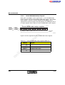
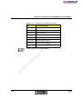
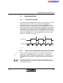
The disk contains the following directories:
\ D D D K M P M
\ S Y S
co
\ U S R
m
\ IB _ IN C
\ IB P C IM P M .S Y S
s.
\ V X W O R K S
ne
nt
\ D D I
\ S Y S T E M
\ E X A M P L E
6 1 8 9 A 0 0 2
om
po
Figure 1-1 Disk directory structure
Table 1-1
Directory contents
on
l
in
ec
Directory Name
1-4
Contents
IBPCIMPM.SYS
Contains the C source code for the driver.
SYS
Contains adaptations to various systems
USR
Contains include files for various systems
DDI
Contains the Device Driver Interface for VxWorks
SYSTEM
VxWorks system initialization for the IBS PCI SC/..
EXAMPLE
Contains example programs that use a finished
driver.
6189A
Introduction
Table 1-2
Files in the "IBPCIMPM.SYS" directory
Contents
startup.c
Initialization of hardware and software
drvinits.c
Driver initialization routines
vxwsys.c
Operating system functions/routines for VxWorks
Ibpcidrv.c
Functions/routines for PCI access
evthndg.c
Functions/routines for event handling
drvlimit.h
Limitation constants (maximum values, etc.)
errlog.h
Macros, constants, etc. for error logging and
debugging
Ibpcidrv.c
Functions/routines for PCI access
os_adapt.h
Operating system-dependent data structures,
macros, and constants
os_inc.h
Load operating system-dependent headers
co
s.
nt
ne
Constants and structures for working with PCI devices
om
pcimsg.h
po
pci_drv.h
m
File Name
in
ec
vxw_data.h
on
l
Table 1-3
6189A
Constants for error messages
Constants and data structures for VXWorks tasks and
priorities
Files in the "IB_INC\SYS" directory
File Name
Contents
compiler.h
Compiler setting definitions
mpm40.h
Definitions of the MPM register addresses and their
bit masks
Ioctl40.h
Definitions for the devIOCtrl driver function
drv_dbg.h
Defines, typedef, and prototypes for DriverDebugInfo
commands
1-5
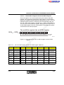
IBS PCI DDK UM E
Table 1-4
Files in the "IB_INC\USR" directory
Contents
stdtypes.h
Generally valid standard type definitions
ddi_err.h
Definitions of possible driver error messages
ddi_usr.h
Defines, typedef, prototypes for DDI basic functions
(without I/O control and management)
ibs_util.h
Declarations of the additional DDI functions, e.g.,
watchdog, read diagnostic registers, etc.
ibddivxw.h
DDI for VxWorks
ddi_macr.h
Macros for messages/data conversion
Svc_code.h
IBS service codes (send/receive)
File Name
Table 1-6
in
ec
File Name
ibspciinit.c
on
l
Table 1-7
1-6
co
s.
nt
ne
Contents
Example program for application of DDI functions
om
simple.c
Files in the "VXWORX\EXAMPLE" directory
po
Table 1-5
m
File Name
Files in the "VXWORX\SYSTEM" directory
Contents
VxWorks system initialization
Files in the "VXWORX\DDI" directory
File Name
Contents
ibddivxw.c
Device Driver Interface (DDI) for VxWorks
6189A
Introduction
1.2
Conditions of Support
m
Upon purchasing this product, you are entitled to comprehensive support
during implementation. This support is available to you free of charge, if
required, for 30 days following registration of the product. This free support
will only be provided via a personal e-mail address, which will be created
for you.
How Can You Obtain This Support?
co
1. Register at the following Internet address:
http://request.phoenixcontact.com/req_eldo/pciddk_d/ddkreg.htm
s.
2. Please complete the registration form in full.
nt
3. As soon as we receive your registration, you will receive confirmation
together with your personal support e-mail address via e-mail.
ne
Points to Note
po
Our free support is available during normal office hours (Germany) and
only via your personal e-mail address.
om
Free support is available for 30 calendar days, commencing on the date of
the confirmation of your registration. The support period may be extended
for a fee. For details, please refer to Section ”Chargeable Support
Services” on page 1-8.
in
ec
Please ensure that you only register the product when you wish to work
continuously on the implementation.
on
l
In general, a fee is charged for telephone and on-site support. For details,
please refer to Section ”Chargeable Support Services” on page 1-8.
In some individual cases, it may be necessary for Phoenix Contact to
telephone you, however, you will not be charged for this.
Our support can only be provided for sources supplied by Phoenix Contact.
As we are not familiar with, and generally do not have access to, your
development environment, Phoenix Contact does not accept any
responsibility or liability for any implementation work affected by this
environment.
Phoenix Contact only accepts liability for products supplied within the
scope of legal requirements for product liability or according to the general
delivery and payment conditions. Phoenix Contact does not accept any
liability for driver implementation developed by you or by a third party.
6189A
1-7
IBS PCI DDK UM E
Phoenix Contact does not accept any responsibility for development,
testing, validation, release, and support of your driver implementation.
1.2.1
Chargeable Support Services
co
m
Using the free support service available via your personal e-mail address,
you can, if necessary, take advantage of other support services. A fee is
charged for these services and we require you to place a written or verbal
order.
Please contact the relevant person in the sales department or your
representative. A direct order cannot be made via your e-mail address.
s.
Extension of the e-mail account for an additional 30 days
Order No. 27 10 26 2
Order Designation IBS PCI DDK SUPPORT EXT
nt
–
on
l
in
ec
om
po
ne
If necessary, we can offer you additional support services tailored to your
requirements. Please contact the relevant person in the sales department
or your representative. We will then be happy to supply you with a personal
quotation.
1-8
6189A
Section 2
This section informs you about
– the PCI register,
– the host interface and
– the MPM for INTERBUS controller boards.
m
Structure and Interfaces of INTERBUS Controller Boards ...................................2-3
PCI Register................................................................................2-4
2.2
Host Interface for INTERBUS Controller Boards ........................2-6
Hardware Settings of Controller Boards ........................2-6
2.2.2
I/O Register....................................................................2-8
s.
2.2.1
nt
Multi-Port Memory (MPM) .........................................................2-16
MPM Address Area......................................................2-19
2.3.2
Segmentation of the SRAM in the MPM ......................2-20
2.3.3
MPM Communication Options .....................................2-21
2.3.4
MPM Hardware Register..............................................2-24
MPM Software Register ...............................................2-48
on
l
in
ec
om
2.3.5
ne
2.3.1
po
2.3
co
2.1
6189A
2-1
2-2
6189A
s.
nt
ne
po
om
in
ec
on
l
co
m
Structure and Interfaces of INTERBUS Controller Boards
2
Structure and Interfaces of INTERBUS Controller
Boards
m
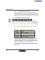
PCI controller boards are directly connected with the host system using
PCI connectors. This hardware interface has (according to the PCI bus
specification 2.2) a 32-bit address and data bus. It has control lines in
addition to the address and data lines. The controller boards support
interrupt operation.
s.
co
A detailed description of the controller board hardware and its installation
in the host system can be found in the IBS PCI SC QS UM E Quick Start
Guide (Order No. 26 98 14 8).
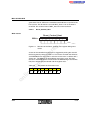
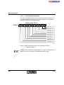
IB S P C I S C /I-T
on
l
1 6 b y te s
0 k b y te s
2 5 6 k b y te s
x + 2 5 6 k b y te s
R r e e s s e e r rv v i e r d t
IB S P C I S C /I-T
x = n * 2 5 6 k b y te s
6 4 k b y te s
M P M
6 1 8 9 A 0 0 3
0 m b y te s
Figure 2-1
6189A
M e m o ry a re a
om
a re a
in
ec
I/O
po
ne
nt
The software interface of the controller boards to the host system consists
of a 16-byte window in the I/O area and a 256-kbyte window in the standard
address area (memory area). The base addresses of both windows are
specified by the system BIOS.
6 1 8 9 A 0 0 4
Controller board address windows in the host system
2-3
IBS PCI DDK UM E
2.1
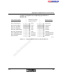
PCI Register
PCI registers integrate the controller boards into a PCI bus system. The
following table shows the arrangement of the PCI registers and their
controller board-specific settings.
Table 2-1
PCI register
Device ID
(0002hex for IBS PCI SC...)
Vendor ID
(1442hex for Phoenix Contact)
04hex
Status register
Command register
Latency timer
Cache line
size
14hex
Base address register 1
(here: addresses for MPM and NV-RAM, 256 kbytes)
po
ne
Base address register 0
(here: I/O address for the host interface register)
Base address register 2 (not used)
Base address register 3 (not used)
om
1Chex
20hex
Base address register 4 (not used)
24hex
Base address register 5 (not used)
28hex
Reserved (not used)
in
ec
on
l
Header type
Revision ID
(HW Rev)
10hex
18hex
Comments for the
table
s.
Bits
nt
0Chex
co
Class code
(0Chex)
08hex
m
00hex
2Chex
Reserved (not used)
30hex
Base address expansion memory (expansion ROM)
(not used)
34hex
Reserved (not used)
38hex
Reserved (not used)
3Chex
Max-Lat
(00hex)
Min-Gnt
(00hex)
Interrupt pin
Interrupt line
The vendor ID 1442hex is the approved manufacturer identifier for
Phoenix Contact.
The device ID of boards with the file designation IBS PCI SC... is 0002hex.
2-4
6189A
Structure and Interfaces of INTERBUS Controller Boards
The revision ID indicates the hardware revision of the controller board.
Class code 0Chex indicates a serial bus controller.
The PCI interface uses two base address registers:
Base address register 0 contains the I/O addresses for the host interface
register. The length of the I/O address area is 16 bytes.
m
Base address register 1 is used for the MPM address area of the master
and NV-RAM. A 128-kbyte memory address area is provided for the MPM
and NV-RAM respectively.
co
The MPM acts as a data interface between the host system and the
INTERBUS master (see also Section 2.3, "Multi-Port Memory (MPM)").
on
l
in
ec
om
po
ne
nt
s.
Only interrupt line A is used.
6189A
2-5
IBS PCI DDK UM E
2.2
Host Interface for INTERBUS Controller
Boards
The host interface forms the interface between the host system and the
controller board MPM. The host interface also contains several registers.
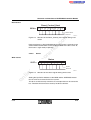
Hardware Settings of Controller Boards
m
2.2.1
nt
s.
co
IBS PCI controller boards have DIP switches for setting controller board
numbers (board number) and the test mode (ON/OFF). The transmission
rate (500 kbaud/2 Mbaud) can also be set for the IBS PCI SC/RI-LK
controller board.
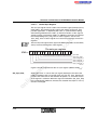
6
5
4
po
7
3
2
1
in
ec
om
8
ne
O F F
on
l
Figure 2-2
2-6
O N
C o n tr o lle r b o a r d n u m b e r s
R e s e rv e d
T r a n s m is s io n r a te
T e s t m o d e
6 1 8 9 A 0 0 5
DIP switch assignment
As default upon delivery, all DIP switches are in the OFF position. DIP
switches 4 to 6 are reserved for later function expansions and should be
left in the OFF position.
6189A
Structure and Interfaces of INTERBUS Controller Boards
The controller board number (board number) is specified using DIP
switches 1 to 3. Table 2-2 indicates possible settings:
DIP Switch 1
DIP Switch 2
DIP Switch 3
1
OFF
OFF
OFF
2
OFF
OFF
ON
3
OFF
ON
OFF
4
OFF
ON
ON
5
ON
OFF
OFF
6
ON
7
8
s.
m
Board Number
ON
ON
ON
OFF
ON
ON
ON
nt
OFF
If DIP switch 8 is in the ON position, after startup the controller board will
automatically switch to test mode and start up any connected bus. In test
mode, data exchange is not possible in either direction between the host
system and the MPM. No outputs are set.
om
po
Test mode
Possible settings for controller board numbers
co
Table 2-2
ne
Board number
in
ec
Test mode may only be used for checking the INTERBUS system
connected to the controller board. Test mode should not be used in normal
system operation.
For the IBS PCI SC/RI-LK only:
on
l
Transmission rate
6189A
The transmission rate of the INTERBUS system is set, during operation via
optical fiber cable, using DIP switch 7. If the DIP switch is in the OFF
position, the transmission rate is 500 kbaud. If the DIP switch is in the ON
position, INTERBUS data is transmitted at 2 Mbaud.
This switch has no significance for controller boards IBS PCI SC/I-T and
IBS PCI SC/RI/I-T and should remain in the OFF position. The baud rate
setting is made automatically.
2-7
IBS PCI DDK UM E
2.2.2
I/O Register
The controller board occupies 16 I/O addresses of the host system. The
first eight addresses are occupied with control registers, which can be both
read and written. After the control registers come the I/O registers for direct
inputs and outputs.
Function
0
Board_Number
Read current set controller board number
1
Not_Used
Reserved
2
IRQ_Control_Host
Interrupt enable
3
WDT_Control_Host
Status, enabling, and reset of the watchdog timer
4
Reset_Control_Host
Master software reset
5
Not_Used
Reserved
6
Not_Used
Reserved
7
Status
Read and write status register
8
Direct_IN
Read inputs Direct IN 1 to Direct IN 6
9
Direct_OUT
10
Not_Used
11
Not_Used
Reserved
12
Not_Used
Reserved
13
Not_Used
Reserved
Not_Used
Reserved
Not_Used
Reserved
15
2-8
on
l
14
om
po
ne
nt
s.
co
Name
in
ec
Offset
Addresses of the I/O registers
m
Table 2-3
Read and write outputs Direct OUT 1 and Direct OUT 2
Reserved
6189A
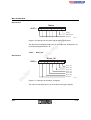
Structure and Interfaces of INTERBUS Controller Boards
2.2.2.1
Board_Number
B o a rd _ N u m b e r
0 0 0 0
h e x
D 7
D 6
D 5
D 4
D 3
D 2
D 1
D 0
B o a rd N u m b e r (0 ...7 )
Figure 2-3
Structure of the Board_Number register
The Board_Number register reads the current controller board numbers
(Board_Number) set using DIP switches 1 to 3. Reserved bits are reported
with a "0".
ne
nt
s.
Read access
6 1 8 9 A 0 0 6
co
m
R e s e rv e d
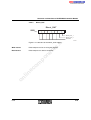
IRQ_Control_Host
po
2.2.2.2
IR Q _ C o n tr o l_ H o s t
om
0 0 0 2
in
ec
h e x
on
l
Figure 2-4
Write access
D 7
D 6
D 5
D 4
D 3
D 2
D 1
D 0
R e s e rv e d
IR Q _ E n a b le
R e s e rv e d
6 1 8 9 A 0 0 7
Structure of the IRQ_Control_Host register
In the IRQ_Control_Host register, the interrupt request line, which is used
by the host system, is enabled. The interrupt is completed by resetting the
host interface and can - if necessary - be enabled by the driver software.
The selected interrupt request line is enabled if the IRQ_Enable bit
receives the value "1".
The reserved bits must contain the value "0".
Read access
6189A
The IRQ_Enable bit can be read back. All other bits receive the value "0".
2-9
IBS PCI DDK UM E
2.2.2.3
Write access
WDT_Control_Host
The host interface watchdog timer can be switched on, operated, and reset
using the WDT_Control_Host register. The reserved bits must contain the
value "0".
h e x
D 7
D 6
D 5
D 4
D 3
D 2
D 1
D 0
W D T _ In te rv a l
W D T _ C le a r
R e s e rv e d
6 1 8 9 A 0 0 8
Structure of the WDT_Control_Host register during write
access
po
Figure 2-5
W D T _ E n a b le
R e s e rv e d
ne
nt
s.
co
0 0 0 3
m
W D T _ C o n tr o l_ H o s t
on
l
in
ec
om
Setting the WDT_Enable bit activates the watchdog timer. This timer is
active and runs until it overflows or is switched off by a hardware reset of
the host system. It cannot be deactivated by resetting the WDT_Enable
bit. The monitoring time is determined by a bit combination in the
"WDT_interval" (D2 to D4). The contents of this field are saved when the
watchdog timer is switched on and can be modified while the timer is active.
The watchdog timer is triggered by the read and write access of the
WDT_Control_Host register. The WDT_Clear status is not saved, i.e., the
watchdog timer cannot be switched off by setting this bit. WDT_Clear only
resets the WDT_Status bit and the HF LED on the controller board after a
watchdog timer has been triggered.
2-10
6189A
Structure and Interfaces of INTERBUS Controller Boards
In the WDT_Interval (data bits 2 to 4) the following monitoring times can be
set:
WDT_Interval
D3
D2
Monitoring Time
0
0
0
8.2 ms
0
0
1
16.4 ms
0
1
0
32.8 ms
0
1
1
65.5 ms
1
0
0
131.1 ms
1
0
1
262.1 ms
1
1
0
524.3 ms
1
1
1
nt
s.
co
D4
m
Table 2-4
po
ne
1048.6 ms
om
Read access
h e x
on
l
in
ec
0 0 0 3
D 7
W D T _ C o n tr o l_ H o s t
D 6
D 5
D 4
D 3
D 2
D 1
D 0
W D T _ E n a b le
W D T _ S ta tu s
W D T _ In te rv a l
W D T _ C le a r
R e s e rv e d
6 1 8 9 A 0 0 9
Figure 2-6
Structure of the WDT_Control_Host register during read
access
During a read access, the WDT_Enable bit indicates whether the watchdog
timer is running. This bit cannot be reset by a write access. The
WDT_Status bit indicates the status of the monitoring output. If the bit has
the value "0", the watchdog timer has always been triggered appropriately
since power up. If the bit has the value "1", the watchdog timer was not
reset in the specified time. In this case, the interrupt SRQ2L(0) is
6189A
2-11
IBS PCI DDK UM E
generated. The HF LED on the controller board indicates a SysFail of the
host system. This bit remains set until WDT_Clear is set or the timer is
restarted. The set time interval WDT_Interval can be read back.
2.2.2.4
Reset_Control_Host
Write access
D 7
h e x
D 6
D 5
D 4
D 3
D 2
D 1
D 0
6 1 8 9 A 0 1 0
Structure of the Reset_Control_Host register during write
access
ne
nt
Figure 2-7
R e s e t
s.
co
0 0 0 4
m
R e s e t_ C o n tr o l_ H o s t
om
po
A reset of the controller board master is triggered by writing the reset bit
field using the bit pattern in Table 2-5. This means that both the firmware
and INTERBUS are reset. After a reset the master starts a selftest with a
"power on". The MPM is not immediately reset with a reset. The data
remains in the MPM until the master checks the MPM during its test routine.
Only then will the data be cleared and the register reset.
Table 2-5
Bit pattern for the master reset
D6
D5
D4
D3
D2
D1
D0
1
1
0
0
1
0
1
0
on
l
in
ec
D7
2-12
6189A
Structure and Interfaces of INTERBUS Controller Boards
Read access
R e s e t_ C o n tr o l_ H o s t
0 0 0 4
D 7
h e x
D 6
D 5
D 4
D 3
D 2
D 1
D 0
M a s te r s e lfte s t
R e s e rv e d
m
6 1 8 9 A 0 1 1
Structure of the Reset_Control_Host register during read
access
co
Figure 2-8
2.2.2.5
Status
in
ec
om
po
Write access
0 0 0 7
h e x
on
l
Figure 2-9
6189A
ne
nt
s.
During read access, data bit D0 indicates that the master is currently in the
selftest mode and therefore cannot enable the MPM. If the bit is set to "0",
the master is again ready to operate.
D 7
D 6
D 5
S ta tu s
D 4
D 3
D 2
D 1
D 0
S y s fa il
R e s e rv e d
6 1 8 9 A 0 1 4
Structure of the status register during write access
Setting the SysFail bit indicates to the MPM and the INTERBUS master
that an error has occurred in the host system.
This bit is set after startup. If the bit is set, no output data can be sent to the
bus. Therefore this bit must be reset by the driver software.
2-13
IBS PCI DDK UM E
Read access
S ta tu s
0 0 0 7
h e x
D 7
D 6
D 5
D 4
D 3
D 2
D 1
D 0
S y s fa il
M P M _ R e a d y L
m
R e s e rv e d
6 1 8 9 A 0 1 5
co
Figure 2-10 Structure of the status register during read access
Direct_IN
h e x
D 7
D 6
D 5
D ir e c t_ IN
D 4
D 3
D 2
D 1
on
l
in
ec
om
0 0 0 8
po
Read access
ne
2.2.2.6
nt
s.
The SysFail bit and MPM_ReadyL bit can be read back. All other bits are
reserved and reported with a "0".
D 0
D ir e c t_ IN _ 1
D ir e c t_ IN _ 2
D ir e c t_ IN _ 3
D ir e c t_ IN _ 4
D ir e c t_ IN _ 5
D ir e c t_ IN _ 6
R e s e rv e d
6 1 8 9 A 0 1 6
Figure 2-11 Structure of the Direct_IN register
The status of the direct inputs can be read back using this register.
2-14
6189A
Structure and Interfaces of INTERBUS Controller Boards
2.2.2.7
Direct_OUT
D ir e c t_ O U T
0 0 0 9
h e x
D 7
D 6
D 5
D 4
D 3
D 2
D 1
D 0
D ir e c t_ O U T _ 1
m
D ir e c t_ O U T _ 2
co
R e s e rv e d
6 1 8 9 A 0 1 7
s.
Figure 2-12 Structure of the Direct_OUT register
Direct outputs can be set using this register.
Read access
Direct outputs can also be read back.
on
l
in
ec
om
po
ne
nt
Write access
6189A
2-15
IBS PCI DDK UM E
2.3
Multi-Port Memory (MPM)
co
m
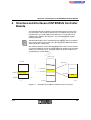
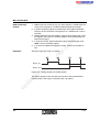
Along with the INTERBUS master and the host interface, the multi-port
memory (MPM) is a central component of INTERBUS controller boards. As
described above, all information exchanged between the host system and
the INTERBUS master is routed through the MPM.
M P M
s.
H o s t
in te r fa c e
po
ne
nt
P C I
r e g is te r
IN T E R B U S
m a s te r
IN T E R B U S
c o n tr o lle r b o a r d
6 1 8 9 A 0 1 2
in
ec
om
H o s t (P C )
on
l
Figure 2-13 The MPM as the central interface of the controller board
The MPM control logic ensures prioritized assignment of access to the
MPM. Time monitoring is started in parallel with accessing of the MPM. If
a device takes too long to access or fails to access, a timeout is generated.
This is indicated in an MPM register and access to the MPM is
simultaneously re-enabled for other devices.
All data in the MPM is stored in Intel format ("little-endian" or "low-high"
format). Appropriate conversion is therefore required on host system
access.
2-16
6189A
Structure and Interfaces of INTERBUS Controller Boards
In addition to the hardware registers, the MPM has a series of software
registers, which are used specifically to control mailbox communication
between the individual devices. The number and location of these registers
are not predetermined by the hardware.
Static RAM (SRAM)
–
Memory manager
–
Status and control register
–
Serial data channel
s.
co
–
m
From the viewpoint of the user, the MPM therefore consists of the following
functional components:
The static RAM (SRAM) uses MPM address area 0000hex through FFFFhex
and therefore occupies a special position within the MPM. This area is
always available and cannot be blocked by the MPM memory manager.
The SRAM contains the data area (DTA) and the mailbox area (MXA), i.e.,
all data exchanged between the individual nodes is routed via the SRAM.
The segmentation and size of the individual areas is specified by the MPM
firmware manager rather than being predetermined by the hardware.
Memory manager
The entire MPM address area is a maximum of 512 kbytes. Address area
00000hex through 0FFFFhex (64 kbytes) occupies a special position. This
area contains the static RAM (SRAM) and the hardware registers. Up to
256 pages of any size can be displayed in the remaining area
(10000hex –7FFFFhex). It is possible to switch between the individual pages
using a special hardware register in the MPM. Each node can display the
relevant page independently of the other nodes. Address area 0000hex
through FFFFhex (64 kbytes) is not switched with the rest and is thus
available for every page.
on
l
in
ec
om
po
ne
nt
Static RAM
Status and control
register
6189A
MPM address area 3F90hex through 3FFFhex (i.e., within the SRAM area)
contains a series of hardware registers. These registers contain, for
example, MPM status information or are used to evaluate and generate
signals (interrupts) between the individual nodes. The registers are
available to all nodes. Registers that present the same contents to all
nodes are distinguished from those that are dedicated to each individual
node. However, the same number of registers at the same addresses are
always available to all nodes.
2-17
IBS PCI DDK UM E
I/O shift registers and a serial EEPROM can be connected to the MPM
serial data channel. The serial data channel is used to read and save or
output configuration data. A distinction is made between access to the
serial EEPROM and access to the shift registers. For example, the
switches, the motherboard ID, and the MPM configuration are read via the
shift registers. The serial data channel is accessed using four hardware
registers in the MPM.
on
l
in
ec
om
po
ne
nt
s.
co
m
Serial data channel
2-18
6189A
Structure and Interfaces of INTERBUS Controller Boards
2.3.1
MPM Address Area
7 F F F F
P a g e 0 to p a g e 2 5 5
h e x
co
h e x
h e x
h e x
h e x
ne
1 0 0 0 0
0 F F F F
nt
1 9 2 K b y te s
6 4 K b y te s
h e x
S ta tic R A M
po
0 0 0 0 0
s.
4 0 0 0 0
3 F F F F
m
m a x . 2 5 6 K b y te s
(S R A M )
5 8 0 2 A 0 0 2
om
Figure 2-14 MPM address area
in
ec
The diagnostic registers, for example, have the following addresses:
on
l
Register
Address
Diagnostic status register
3520hex
Diagnostic parameter register
3522hex
Ext. diagnostic parameter register
37E6hex
Slave diagnostic status register
37EChex
For additional information on the diagnostic registers, please refer to the
Firmware Services and Error Messages User Manual
IBS SYS FW G4 UM E, Order No. 27 45 18 5.
6189A
2-19
IBS PCI DDK UM E
2.3.2
Segmentation of the SRAM in the MPM
The SRAM is located from address 0000hex through address FFFFhex in
the MPM.
h e x
h e x
h e x
S o ftw a r e r e g is te r
h e x
h e x
ne
3 2 0 0
3 1 F F
H a r d w a r e r e g is te r
s.
3 F 0 0
3 E F F
h e x
h e x
nt
4 0 0 0
3 F F F
co
E x te n d e d D T A
a n d /o r
m a ilb o x a r e a ( M X A )
m
F F F F
in
ec
om
po
E x te n d e d D T A
a n d /o r
m a ilb o x a r e a ( M X A )
2 0 0 0
1 F F F
h e x
h e x
D a ta a re a (D T A )
0 0 0 0
5 8 0 2 A 0 0 3
h e x
on
l
Figure 2-15 Segmentation of the SRAM
This document provides a general description of the MPM, i.e., the
registers and MPM functions of a complete MPM with four nodes are
described.
The IBS PCI controller board MPM is only designed for two nodes:
Node 0:
Host CPU (application program)
Node 1:
INTERBUS master (firmware)
All MPM registers and bits are only available to nodes 0 and 1. Accessing
the registers for nodes 2 and 3 has no effect.
2-20
6189A
Structure and Interfaces of INTERBUS Controller Boards
2.3.3
MPM Communication Options
Communication Methods Used:
Data interface
–
Mailbox interface
–
SysFail requests
–
Signal interface
–
Synchronization requests
on
l
in
ec
om
po
ne
nt
s.
–
co
m
The MPM is used to exchange information between devices (nodes). This
communication can be related to the exchange of data or notification of an
event. Both options are offered by the MPM and are supported by
corresponding mechanisms. The MPM SRAM is available for exchanging
data. For exchanging events, there are four sources of interrupts for each
node, which can be evaluated independently of each other. It is also
possible for both forms to be used in combination, as, for example, in the
mailbox interface.
D a ta a re a
M P M
M a ilb o x a r e a
M a ilb o x h a n d s h a k e in te r r u p t
S y s F a il in te r r u p t
S ig n a l in te r r u p t
S y n c h r o n iz a tio n in te r r u p t
5 8 0 2 A 0 0 4
Figure 2-16 Diagram of the various MPM communication options
6189A
2-21
IBS PCI DDK UM E
2.3.3.1
Data Interface (DTI)
Process data is exchanged with the INTERBUS master via the data
interface.
Various areas are defined within the data area (DTA). The data interface
(DTI) consists of both the "normal" data area, which contains process data
and the extended data area, in which user-specific data can be stored.
s.
co
m
No handshake is specified for exchanging data via the DTI. This means
that in contrast to message exchange via the mailbox interface, data may
be overwritten by one node while it is being read by another. The user must
use their own transmission protocol. For IBS PCI controller boards, a
protocol of this type is activated by default by the firmware, and is
supported by the driver.
2.3.3.2
ne
nt
A detailed description of the data interface can be found in Section 3, "Data
Exchange via the Data Area".
Mailbox Interface (MXI)
po
The mailbox interface (MXI) is a protocol-oriented interface via which
messages can be exchanged between the nodes.
on
l
in
ec
om
The mailbox interface consists of the mailbox area (MXA) and a number of
hardware and software registers for each node. The area occupied by the
mailbox area and the register addresses is predefined and must not be
changed by the user. The size and location of the mailbox area and the
software registers are specified in the MPM descriptor, which is created by
the MPM master for each node (see Section "Structure of the MPM
Descriptor" on page 2-49).
The mailbox area in turn is divided into a number of blocks ("mailboxes").
Each of these can take one message. When sending, the address of the
mailbox containing the message is placed in a software register in the MPM
and the receiving node is notified (see also Section 4, "Communication via
the Mailbox Interface"). The mailbox is managed by the node driver. The
length of one mailbox is 1 kbyte.
MPM registers used:
2-22
–
Set HS Ax/Bx register
–
Status register 1
–
Handshake register A / handshake register B
–
Send vector and acknowledge vector registers (software registers)
6189A
Structure and Interfaces of INTERBUS Controller Boards
A detailed description of the mailbox interface and the handshake protocol
used can be found in Section 4, "Communication via the Mailbox
Interface".
2.3.3.3
SysFail Request
MPM registers used:
ne
nt
s.
co
m
The SysFail logic can be used to immediately notify other nodes of serious
system errors. The SysFail signal can be triggered either by hardware, via
the corresponding MPM control lines or by software, by writing to a special
MPM register. An interrupt is always generated at all nodes (apart from the
initiating one) and indicated in an MPM register (status register 1). In the
case of a SysFail initiated by the hardware, the logical status of the initiating
line is indicated in a different MPM register (status SysFail register). The
response to a SysFail interrupt depends on the particular node. In the event
of a SysFail interrupt, the INTERBUS master, for example, sets all output
data to zero. A node must acknowledge that it has detected a SysFail
interrupt by writing to an MPM register (clear status bit register). This resets
the corresponding bit in status register 1.
Status register 1
–
Status SysFail register
–
Clear-status-bit register
–
Set SysFail request register
on
l
in
ec
om
po
–
6189A
2-23
IBS PCI DDK UM E
2.3.4
MPM Hardware Register
MPM hardware registers are displayed in the MPM SRAM address area in
3F90hex through 3FFFhex. A distinction is made between read and write
hardware registers.
The write registers are word registers that can initiate or pass on
information or actions. The contents of the write registers can only be read
back in summarized form in the read registers.
Read registers
The read registers are word registers. They can be used to read both the
written data in the write registers and additional status and configuration
data.
Address
Register
Page
Address
Register
3F90hex
Set MPM node par ready 0
2-31
3FCAhex
Set HS A15
2-37
3F92hex
Set MPM node par ready 1
2-31
3FCChex
Set HS B7
2-37
3F94hex
Set MPM node par ready 2
2-31
3FCEhex
Set HS B15
2-37
3F96hex
Set MPM node par ready 3
2-31
3FD0hex
Set HS A2
2-37
3F98hex
Switch memory
2-42
3FD2hex
Set HS A10
2-37
3F9Chex
Set sync req
2-41
3FD4hex
Set HS B2
2-37
3FA0hex
Set SysFail req
2-33
3FD6hex
Set HS B10
2-37
3FA2hex
Program bits
2-45
3FD8hex
Set HS A6
2-37
on
l
in
ec
om
ne
Write register addresses in the MPM
po
Table 2-6
nt
s.
co
m
Write registers
Page
3FA4hex
Serial data
2-44
3FDAhex
Set HS A14
2-37
3FA6hex
Serial address
2-43
3FDChex
Set HS B6
2-37
3FA8hex
Clear status bit 0
2-34
3FDEhex
Set HS B14
2-37
3FAAhex
Clear status bit 1
2-34
3FE0hex
Set HS A1
2-37
3FAChex
Clear status bit 2
2-34
3FE2hex
Set HS A9
2-37
3FAEhex
Clear status bit 3
2-34
3FE4hex
Set HS B1
2-37
3FB0hex
Set MPM node SG int 0
2-38
3FE6hex
Set HS B9
2-37
2-24
6189A
Structure and Interfaces of INTERBUS Controller Boards
Write register addresses in the MPM
Address
Register
Set MPM node SG int 1
2-38
3FE8hex
Set HS A5
2-37
3FB4hex
Set MPM node SG int 2
2-38
3FEAhex
Set HS A13
2-37
3FB6hex
Set MPM node SG int 3
2-38
3FEChex
Set HS B5
2-37
3FB8hex
Set MPM node ready0
2-30
3FEEhex
Set HS B13
2-37
3FBAhex
Set MPM node ready1
2-30
3FF0hex
Set HS A0
2-37
3FBChex
Set MPM node ready2
2-30
3FF2hex
Set HS A8
2-37
3FBEhex
Set MPM node ready3
2-30
3FF4hex
Set HS B0
2-37
3FC0hex
Set HS A3
2-37
3FF6hex
Set HS B8
2-37
3FC2hex
Set HS A11
2-37
3FF8hex
Set HS A4
2-37
3FC4hex
Set HS B3
3FC6hex
Set HS B11
3FC8hex
Set HS A7
Table 2-7
s.
nt
Page
ne
3FB2hex
2-37
3FFAhex
Set HS A12
2-37
2-37
3FFChex
Set HS B4
2-37
2-37
3FFEhex
Set HS B12
2-37
po
Register
om
Address
m
Page
co
Table 2-6
Read register addresses in the MPM
Register
Page
Address
Register
Page
3F90hex
MPM configuration
2-26
3FB2hex
Status SysFail
2-32
3F98hex
Read memory page
2-43
3FB4hex
Status node SG inf
2-40
3FA2hex
RDY bits
2-46
3FB6hex
Status register 2
2-29
3FA4hex
Serial data
2-44
3FC0hex
Handshake register A
2-35
3FB0hex
Status register 1
2-27
3FC2hex
Handshake register B
2-35
on
l
in
ec
Address
6189A
2-25
IBS PCI DDK UM E
2.3.4.1
MPM Configuration Register
The MPM configuration register enables the nodes to read the board
configuration. The register contains information about the size of the MPM
and the status of the nodes.
h e x
1 5
1 4
1 3
1 2
1 1
1 0
9
8
7
6
5
4
3
2
1
0
M P
M P
M P
M P
R e
G e
R e
F u
R e
M P
M _ N o
M _ N o
M _ N o
M _ N o
s e rv e d
n e ra te
s e rv e d
n c tio n _
s e rv e d
M _ S iz
ne
nt
s.
co
3 F 9 0
c o n fig u r a tio n
m
M P M
d e
d e
d e
d e
_ P
_ P
_ P
_ P
a r
a r
a r
a r
_ R
_ R
_ R
_ R
e a
e a
e a
e a
d y
d y
d y
d y
_ 0
_ 1
_ 2
_ 3
_ H o s t_ B u s _ T im e o u t
D e c o d e r_ P re s e n t
e
po
5 8 0 2 A 0 0 5
om
Figure 2-17 Bit assignment for the MPM configuration register
(address 3F90hex)
Bits 14 and 15 in the MPM configuration register indicate the size of the
SRAM available for the MPM:
in
ec
MPM_Size
Table 2-8
Setting the MPM size
on
l
Address Area
MPM_Node_Par_Ready_x
2-26
Bit 14
Bit 15
16 kbytes
0
0
64 kbytes
0
1
256 kbytes
1
0
512 kbytes
1
1
The MPM_Node_Ready_x bit indicates that the node has successfully
completed its selftest (bit = 1: selftest successful). These bits are set by the
nodes by writing the value 8000hex to the set MPM node ready x register
and reset with the value 0000hex.
6189A
Structure and Interfaces of INTERBUS Controller Boards
2.3.4.2
Status Register 1
Bit 12 - bit 15
Node 1:
Bit 8 - bit 11
Node 2:
Bit 4 - bit 7
Node 3:
Bit 0 - bit 3
S ta tu s r e g is te r 1
1 5
1 4
1 3
1 2
1 1
1 0
9
8
7
6
5
4
po
om
in
ec
on
l
MPM_Node_Ready_x
6189A
3
2
nt
h e x
ne
3 F B 0
s.
co
Node 0:
m
Status register 1 contains information about the status of the individual
nodes. It contains four bits for each node:
1
0
S y s _ F a il_ 3
H S _ IN T _ 3
R e s e rv e d
M P M _ N o d
S y s _ F a il_ 2
H S _ IN T _ 2
R e s e rv e d
M P M _ N o d
S y s _ F a il_ 1
H S _ IN T _ 1
R e s e rv e d
M P M _ N o d
S y s _ F a il_ 0
H S _ IN T _ 0
R e s e rv e d
M P M _ N o d
e _ R e a d y _ 3
e _ R e a d y _ 2
e _ R e a d y _ 1
e _ R e a d y _ 0
5 8 0 2 A 0 0 6
Figure 2-18 Bit assignment for status register 1 (address 3FB0hex)
The MPM_Node_Ready_x bit indicates that the node has successfully
completed its selftest (bit = 1: selftest successful). These bits are set by the
nodes by writing the value 8000hex to the set MPM node ready x register
and reset with the value 0000hex.
2-27
IBS PCI DDK UM E
Setting the HS_Int_x bit in status register 1 indicates to the node that there
is a message ready for it in the MPM (see Section 4, "Communication via
the Mailbox Interface"). The bit can be used in polling mode or in an
interrupt routine to locate the cause of the interrupt more precisely and is a
summary of the handshake bits for the node.
Sys_Fail_x
The Sys_Fail_x bit is used to indicate a serious malfunction of a node. The
Sys_Fail_x bit is set by the hardware or the set SysFail register and has to
be reset by the nodes by writing the value 0000hex to the clear status
SysFail x registers. The status SysFail register can be used to determine
which node has signaled the system error.
co
m
HS_Int_x
on
l
in
ec
om
po
ne
nt
s.
The Sys_Fail_x bits do not indicate the status of the line that has initiated
the SysFail.
2-28
6189A
Structure and Interfaces of INTERBUS Controller Boards
2.3.4.3
Status Register 2
Bit 12 - bit 15
Node 1:
Bit 8 - bit 11
Node 2:
Bit 4 - bit 7
Node 3:
Bit 0 - bit 3
S ta tu s r e g is te r 2
1 5
1 4
1 3
1 2
1 1
1 0
9
8
7
6
5
4
3
2
1
0
nt
h e x
in
ec
om
po
ne
3 F B 6
s.
co
Node 0:
m
Status register 2 contains additional information about the status of the
individual nodes. For each node, four bits are provided in the register:
S y
M P
T im
S y
M P
T im
S y
M P
T im
S y
M P
T im
n c
M
e
n c
M
e
n c
M
e
n c
M
e
_ R
_ T
o u
_ R
_ T
o u
_ R
_ T
o u
_ R
_ T
o u
e
im
t_
e
im
t_
e
im
t_
e
im
t_
q _ 3
e o u
N o d
q _ 2
e o u
N o d
q _ 1
e o u
N o d
q _ 0
e o u
N o d
t_ N o d e _ 3
e
t_ N o d e _ 2
e
t_ N o d e _ 1
e
t_ N o d e _ 0
e
5 8 0 2 A 0 0 7
Figure 2-19 Bit assignment for status register 2 (address 3FB6hex)
on
l
Sync_Req_x
6189A
Setting the Sync_Req_x bit (bit = 1) in status register 2 indicates that the
sync interrupt has been generated for the associated node. It is not
possible to determine which node has caused the sync interrupt. The
sync_req bit is reset by writing set bit 14 to the clear status bit register.
Each node can only clear its own bit, i.e., node 1, for example, can only
reset the Sync_Req_1 bit.
2-29
IBS PCI DDK UM E
2.3.4.4
The Set MPM Node Ready x Register
Writing the value 8000hex (most significant bit = 1) to a Set MPM node
ready x register sets the corresponding MPM_Node_Ready_x bit in MPM
status register 1. The bit is reset by writing the value 0000hex (most
significant bit = 0) to the register. By setting the bit, the node signals that it
is ready to operate. Each node has its own set MPM node ready x register.
h e
h e x
,
1 5
1 4
9
1 3
1 2
1 1
1 0
8
7
6
h e x
5
4
3
2
m
, 3 F B A
x , 3 F B E
1
co
h e x
n o d e r e a d y x r e g is te r
0
N o t u s e d
S e t b it
5 8 0 2 A 0 0 8
nt
s.
3 F B 8
3 F B C
T h e s e t M P M
The set MPM node ready x register addresses
po
Table 2-9
ne
Figure 2-20 Bit assignment for the set MPM node ready x register
Register
3FB8hex
Set MPM node ready 0
3FBAhex
Set MPM node ready1
3FBChex
Set MPM node ready2
3FBEhex
Set MPM node ready3
on
l
in
ec
om
Address
2-30
6189A
Structure and Interfaces of INTERBUS Controller Boards
2.3.4.5
The Set MPM Node Par Ready x Register
h e x
,
1 5
1 4
9
1 3
1 2
1 1
1 0
8
h e x
7
6
s.
h e
, 3 F B A
x , 3 F B E
n o d e r e a d y x r e g is te r
5
4
3
2
nt
h e x
T h e s e t M P M
1
0
N o t u s e d
S e t b it
ne
3 F B 8
3 F B C
co
m
After successful parameterization, a node sets the corresponding
MPM_Node_Par_Ready_x bit in the MPM configuration register. This is
achieved by writing a value with a set most significant bit, e.g., the value
8000hex, to the set MPM node par ready x register. Writing a reset bit 15
(bit = 0) to the register also resets the corresponding
MPM_Node_Par_Ready_x bit in the MPM configuration register. Each
node has its own register, which corresponds to the node number (for
example, node 1 uses the set MPM node par ready 1 register).
5 8 0 2 A 0 0 8
The set MPM node par ready x register addresses
om
Table 2-10
po
Figure 2-21 Bit assignment for the set MPM node par ready x register
Register
3F90hex
Set MPM node par ready 0
3F92hex
Set MPM node par ready 1
3F94hex
Set MPM node par ready 2
3F96hex
Set MPM node par ready 3
on
l
in
ec
Address
6189A
2-31
IBS PCI DDK UM E
2.3.4.6
Status SysFail Register
The status SysFail register can be used to determine which node has
signaled a system error (bit = 1: node system error). The bits in the register
correspond to the status of the corresponding SysFail line.
S ta tu s S y s F a il
1 5
1 4
1 3
1 2
1 1
1 0
9
8
7
6
5
4
3
2
1
0
m
h e x
ne
nt
s.
co
3 F B 2
S ta
"0 "
S ta
"0 "
S ta
"0 "
S ta
"0 "
tu s _ S y s _ F a il_ 3
tu s _ S y s _ F a il_ 2
tu s _ S y s _ F a il_ 1
tu s _ S y s _ F a il_ 0
5 8 0 2 A 0 1 0
om
The Status_Sys_Fail_x bit corresponds directly to the hardware signal
used to indicate the system error. It is not possible to reset the bit by writing
to an MPM register. This is only possible once the signal (hardware line)
indicating the error has been withdrawn.
on
l
in
ec
Status_Sys_Fail_x
po
Figure 2-22 Bit assignment for the status Sy^sFail register
(address 3FB2hex)
2-32
6189A
Structure and Interfaces of INTERBUS Controller Boards
2.3.4.7
The Set SysFail Request Register
The SysFail signal can be generated in two different ways: a hardware
signal to the MPM control logic or the software writing to the set SysFail
request register. As with other registers, writing with bit 15 (the most
significant bit) set initiates the signal. This generates a SysFail interrupt on
all other nodes.
1 5
1 4
1 3
1 2
1 1
1 0
9
8
7
6
5
4
3
2
1
co
h e x
0
N o t u s e d
S e t b it
5 8 0 2 A 0 1 1
nt
s.
3 F A 0
m
T h e s e t S y s F a il r e q u e s t R e g is te r
on
l
in
ec
om
po
ne
Figure 2-23 Bit assignment for the set SysFail request register (address
3FA0hex)
6189A
2-33
IBS PCI DDK UM E
2.3.4.8
The Clear Status Bit x Registers
The clear status bit x registers are used to reset certain signals sent
between the nodes. Each node has its own clear status bit x register, i.e.,
for a complete MPM there are four clear status bit x registers.
h e x
h e x
,
1 5
,
1 4
1 3
1 2
1 1
1 0
9
8
7
6
5
4
3
,
2
1
0
m
h e x
co
A 8
A A
A C
A E
h e x
N o
C le
N o
C le
C le
t u
a r
t u
a r
a r
s e d
_ M P M _ T im e o u t
s e d
_ S y n c _ In t
_ S ta tu s _ S y s _ F a il
5 8 0 2 A 0 1 2
nt
s.
3 F
3 F
3 F
3 F
T h e c le a r s ta tu s b it x r e g is te r
Clear status bit x register addresses
po
Table 2-11
ne
Figure 2-24 Bit assignment for the clear status bit x registers
Clear status bit 0
3FAChex
Clear status bit 2
3FAEhex
Clear status bit 3
3FA8hex
3FAAhex
Clear status bit 1
in
ec
on
l
Register
om
Address
As can be seen in Figure 2-24, the following signals can be reset using the
clear status bit x register:
–
MPM timeout
–
Sync signal
–
Status SysFail signal
For each signal to be reset, enter a "1" in the corresponding bit position.
This enables the signals to be reset individually or simultaneously.
2-34
6189A
Structure and Interfaces of INTERBUS Controller Boards
2.3.4.9
Handshake Register A and Handshake Register B
32 handshake bits are defined for exchanging acknowledged messages
between the nodes. The handshake bits are used by the mailbox
handshake protocol for sending, receiving, and acknowledging messages
between the nodes.
co
m
By evaluating handshake registers A and B, a node can determine which
other node has caused which handshake interrupt (see also Section 4,
"Communication via the Mailbox Interface").
H a n d s h a k e r e g is te r A
1 5
1 4
1 3
1 2
1 1
1 0
9
8
7
6
ne
po
om
in
ec
5
4
s.
h e x
nt
3 F C 0
3
2
1
0
H S
H S
H S
H S
H S
H S
H S
H S
H S
H S
H S
H S
H S
H S
H S
H S
_ A
_ A
_ A
_ A
_ A
_ A
_ A
_ A
_ A
_ A
_ A
_ A
_ A
_ A
_ A
_ A
0
1
2
3
4
5
6
7
8
9
1 0
1 1
1 2
1 3
1 4
1 5
5 8 0 2 A 0 1 3
on
l
Figure 2-25 Bit assignment for handshake register A (address 3FC0hex)
6189A
2-35
IBS PCI DDK UM E
H a n d s h a k e r e g is te r B
h e x
1 5
1 4
1 3
1 2
1 1
1 0
9
8
7
6
5
4
3
2
1
0
H S _
H S _
H S _
H S _
H S _
H S _
H S _
H S _
H S _
H S _
H S _
H S _
H S _
H S _
H S _
H S _
B 0
B 1
B 2
B 3
B 4
B 5
B 6
B 7
B 8
B 9
B 1
B 1
B 1
B 1
B 1
B 1
0
1
2
3
4
5
5 8 0 2 A 0 4 0
po
ne
nt
s.
co
m
3 F C 2
on
l
in
ec
om
Figure 2-26 Bit assignment for handshake register B (address 3FC2hex)
2-36
6189A
Structure and Interfaces of INTERBUS Controller Boards
2.3.4.10
The Set HS Ax Register and the Set HS Bx Register
co
m
These 32 registers are used for implementing the mailbox handshake
protocol. The assignment and meaning of the registers are described in
detail in the mailbox handshake protocol. Writing set bit 15 (bit = 1) to a set
HS Ax/Bx register activates an interrupt at the corresponding node, the
HS_INT_x bit in status register 1 changes to "1", and the associated bit is
set in one of the two handshake registers. Writing reset bit 15 (bit = 0) to a
set HS Ax/Bx register resets the associated bit in the handshake register
and terminates the interrupt request.
h e x
- 3 F F E
h e x
1 5
1 4
1 3
1 2
1 1
1 0
9
8
7
6
5
4
3
2
1
0
N o t u s e d
S e t b it
nt
3 F C 0
s.
T h e s e t H S A x r e g is te r / th e s e t H S B x r e g is te r
ne
5 8 0 2 A 0 1 4
Table 2-12
om
po
Figure 2-27 Bit assignment for the set HS Ax register and set HS Bx
register
The set HS Ax register and the set HS Bx register addresses
Register
3FC0hex
Set HS A3
3FC2hex
3FC4hex
Address
Register
Address
Register
Address
Register
3FD0hex
Set HS A2
3FE0hex
Set HS A1
3FF0hex
Set HS A0
Set HS A11
3FD2hex
Set HS A10
3FE2hex
Set HS A9
3FF2hex
Set HS A8
Set HS B3
3FD4hex
Set HS B2
3FE4hex
Set HS B1
3FF4hex
Set HS B0
on
l
in
ec
Address
3FC6hex
Set HS B11
3FD6hex
Set HS B10
3FE6hex
Set HS B9
3FF6hex
Set HS B8
3FC8hex
Set HS A7
3FD8hex
Set HS A6
3FE8hex
Set HS A5
3FF8hex
Set HS A4
3FCAhex
Set HS A15 3FDAhex
Set HS A14
3FEAhex
Set HS A13
3FFAhex
Set HS A12
3FCChex
Set HS B7
3FDChex
Set HS B6
3FEChex
Set HS B5
3FFChex
Set HS B4
3FCEhex
Set HS B15 3FDEhex
Set HS B14
3FEEhex
Set HS B13
3FFEhex
Set HS B12
6189A
2-37
IBS PCI DDK UM E
2.3.4.11
The Set MPM Node SG Int x Register
h e x
h e x
1 5
,
1 4
1 3
1 2
1 1
1 0
9
8
7
6
5
4
3
2
1
0
co
,
h e x
in t x r e g is te r
,
h e x
s.
B 0
B 2
B 4
B 6
n o d e S G
N o
S e
S e
S e
S e
t
t_
t_
t_
t_
u s
N
N
N
N
e d
o d
o d
o d
o d
nt
3 F
3 F
3 F
3 F
T h e s e t M P M
m
The set MPM node SG int x registers can be used to send a signal
(interrupt) to any other nodes. The meaning of this signal is left entirely to
the user. Each node has its own register, which corresponds to the node
number (for example, node 1 uses the set MPM node par ready 1 register).
e _
e _
e _
e _
S G
S G
S G
S G
_ In
_ In
_ In
_ In
t_
t_
t_
t_
3
2
1
0
5 8 0 2 A 0 1 5
Table 2-13
po
ne
Figure 2-28 Bit assignment for the set MPM node SG int x register
The set MPM node SG int x register addresses
Register
3FB0hex
Set MPM node SG int 0
3FB2hex
Set MPM node SG int 1
3FB4hex
Set MPM node SG int 2
3FB6hex
Set MPM node SG int 3
on
l
in
ec
om
Address
The nodes to which a signal is to be sent are selected by the bit pattern
written to the register. A set bit (bit = 1) activates an interrupt at the
corresponding node and sets the associated bit in the status node SG inf
register (see also Section 2.3.4.12, "Status Node SG Inf Register"). A
signal can be sent to one or more nodes simultaneously.
The bits in the status node SG int x register are reset and the interrupt
request cleared by writing a reset bit (bit = 0) to the bit position of the
required node.
2-38
6189A
Structure and Interfaces of INTERBUS Controller Boards
Assignment of register bits to nodes
Function Executed
Bit 15 = 1
Signal to node 0
Bit 14 = 1
Signal to node 1
Bit 13 = 1
Signal to node 2
Bit 12 = 1
Signal to node 3
Bit 15 = 0
Delete signal to node 0
Bit 14 = 0
Delete signal to node 1
Bit 13 = 0
Delete signal to node 2
Bit 12 = 0
Delete signal to node 3
m
Bit
ne
nt
s.
co
Table 2-14
on
l
in
ec
om
po
A node cannot send a signal to itself.
6189A
2-39
IBS PCI DDK UM E
2.3.4.12
Status Node SG Inf Register
The status node SG inf register (status node signal interface register), can
be used to determine from the bit(s) set which node has sent the MPM
node SG int signal to which other node(s).
S ta tu s n o d e S G
h e x
1 5
1 4
1 3
1 2
1 1
1 0
9
8
7
6
5
4
3
2
1
0
om
po
ne
nt
s.
co
m
3 F B 4
in f
N o
N o
N o
N o
N o
N o
N o
N o
N o
N o
N o
N o
N o
N o
N o
N o
d e
d e
d e
d e
d e
d e
d e
d e
d e
d e
d e
d e
d e
d e
d e
d e
_ S
_ S
_ S
_ S
_ S
_ S
_ S
_ S
_ S
_ S
_ S
_ S
_ S
_ S
_ S
_ S
G _
G _
G _
G _
G _
G _
G _
G _
G _
G _
G _
G _
G _
G _
G _
G _
In
In
In
In
In
In
In
In
In
In
In
In
In
In
In
In
t_
t_
t_
t_
t_
t_
t_
t_
t_
t_
t_
t_
t_
t_
t_
t_
3 _
3 _
3 _
3 _
2 _
2 _
2 _
2 _
1 _
1 _
1 _
1 _
0 _
0 _
0 _
0 _
0
1
2
3
0
1
2
3
0
1
2
3
0
1
2
3
5 8 0 2 A 0 1 6
in
ec
Figure 2-29 Bit assignment for the status node SG inf register
(address 3FB4hex)
on
l
In Figure 2-29 the data bits are "Node SG int x y", where "y" designates the
originator and "x" the receiver of the MPM node SG int signal.
2-40
6189A
Structure and Interfaces of INTERBUS Controller Boards
2.3.4.13
The Set Sync Register
m
The set sync register can be used to send a further signal (interrupt) to any
other nodes. The meaning of this signal is left entirely to the user. One
possible application, as implied by the name, is synchronization during
data exchange between the nodes. (In firmware version 4.x this signal is
already used for synchronous mode.) In addition to activating an interrupt,
the corresponding Sync_Req_x bits in status register 2 are set. The
Sync_Req_x bits in status register 2 are reset using the clear status bit x
registers.
co
There is only one register of this type in the MPM. The nodes are, therefore,
always accessed through the same register.
1 5
1 4
1 3
1 2
1 1
1 0
9
8
7
6
4
3
2
1
0
N o
S e
S y
S y
S y
S y
t u s
t_ S
n c _
n c _
n c _
n c _
e d
y n c _
R e q
R e q
R e q
R e q
R
_ B
_ B
_ B
_ B
e q
it_
it_
it_
it_
0
1
2
3
5 8 0 2 A 0 1 7
om
po
5
nt
h e x
ne
3 F 9 C
s.
T h e s e t s y n c r e g is te r
Figure 2-30 Bit assignment for the set sync register (address 3F9Chex)
6189A
Setting this bit to "1" causes the sync signal (interrupt) to be sent to the
nodes according to the sync req bit mask set. The Set_Sync_Req bit can
be set at the same time as the selection bit pattern, i.e., one write access
to the register is sufficient. When the signal is initiated the Set_Sync_Req
bit is automatically withdrawn, whereas the selection mask (bit 15 - bit 12)
remains unchanged.
in
ec
on
l
Set_Sync_Req
2-41
IBS PCI DDK UM E
The nodes to which a signal is to be sent are selected by the bit pattern in
the four most significant bits of the register. A set bit (bit = 1) activates a
sync interrupt at the corresponding node and sets the associated bit in
status register 2 (see also Section 2.3.4.3). A signal can be sent to one or
more nodes simultaneously.
Assignment of the sync req bits to the nodes
Function Executed
Bit 12 = 1
Signal to node 0
Bit 13 = 1
Signal to node 1
Bit 14 = 1
Signal to node 2
Bit 15 = 1
Signal to node 3
s.
The Switch Memory Register
ne
2.3.4.14
co
Bit
m
Table 2-15
nt
Sync_Req_Bit_x
om
po
The MPM address area above FFFFhex can be switched between several
pages. The switch memory register is used to specify which page is
displayed. The pages can be displayed by each node independently of the
other nodes. Thus, for example, node 1 can display page 3, while node 0
works with page 0. It is possible to select from a maximum of 256 pages.
The number of pages depends on the controller board.
in
ec
T h e s w itc h m e m o r y r e g is te r
h e x
on
l
3 F 9 8
1 5
1 4
1 3
1 2
1 1
1 0
9
8
7
6
5
4
3
2
1
0
P a g e n u m b e r
"0 "
5 8 0 2 A 0 1 8
Figure 2-31 Bit assignment for the switch memory register
(address 3F98hex)
The function decoder is also displayed using the switch memory register.
2-42
6189A
Structure and Interfaces of INTERBUS Controller Boards
2.3.4.15
The Read Memory Page Register
As described above, the MPM address area above FFFFhex can be
switched between several pages. For each node, the read memory page
register indicates which page is currently displayed. Each individual node
can display different pages. Thus, for example, node 1 can display page 3,
while node 0 works with page 0.
1 5
1 4
1 3
1 2
1 1
1 0
9
8
7
6
5
4
3
2
1
0
co
h e x
P a g e n u m b e r
"0 "
s.
3 F 9 8
m
T h e r e a d m e m o r y p a g e r e g is te r
nt
5 8 0 2 A 0 1 9
ne
Figure 2-32 Bit assignment for the read memory page register
(address 3F98hex)
Serial Address Register
po
2.3.4.16
in
ec
om
The serial address register is a write register. The register contains the
address for the next serial access. It can be an EEPROM or serial IN/OUT
address. The address is entered as a byte address. When accessing the
serial EEPROM the least significant address bit (0) is not evaluated, as
EEPROM data exchange is word-oriented. However, byte addresses are
always used for serial IN or serial OUT access.
h e x
1 5
1 4
1 3
1 2
1 1
1 0
9
8
7
6
5
4
3
2
1
0
on
l
3 F A 6
S e r ia l a d d r e s s
A 0
A 1
A 2
A 3
A 4
A 5
A 6
N o t u s e d
5 8 0 2 A 0 2 0
Figure 2-33 Bit assignment for the serial address register
(address 3FA6hex)
6189A
2-43
IBS PCI DDK UM E
The following serial address registers are available:
Table 2-16
Serial address register
Address
Register
Page
0002hex
Configuration data
2-46
2.3.4.17
co
m
Only the register address is entered in the serial address register. The
value of the register entered in the serial address register is given in the
serial data register (see page 2-44).
Serial Data Register
ne
nt
s.
The serial data register is used for both write and read access to the MPM
serial channel. It is, therefore, a read/write register. The register contains
either the data to be written or the data that has been read. All 16 bits are
valid when accessing the serial EEPROM. However, when serial IN or
serial OUT is accessed, only the low-order byte (bit 0 to bit 7) is valid.
h e x
1 5
1 4
1 3
1 2
om
3 F A 4
po
S e r ia l d a ta
1 1
1 0
9
8
7
6
5
4
3
2
1
0
D 0 - D 7
D 8 - D 1 5
5 8 0 2 A 0 2 1
on
l
in
ec
Figure 2-34 Bit assignment for the serial data register (address 3FA4hex)
2-44
6189A
Structure and Interfaces of INTERBUS Controller Boards
2.3.4.18
The Program Bits Register
The program bits register is a write register whose four most significant bits
indicate how the serial data channel is to be accessed.
h e x
1 5
1 4
1 3
b its r e g is te r
1 2
7
1 1
1 0
9
8
6
5
4
3
2
1
0
N o
W r
R e
W r
R e
t u
ite
a d
ite
a d
s e
_ S
_ S
_ S
_ S
d
e r ia
e r ia
e r ia
e r ia
l_
l_
l_
l_
E E P R O M
E E P R O M
O u t
In
5 8 0 2 A 0 2 2
s.
co
m
3 F A 2
T h e p ro g ra m
Bit
Bit 15 = 1
Function Executed
Read data from serial IN
Write data to serial OUT
om
Bit 14 = 1
Meaning of the bits
po
Table 2-17
ne
nt
Figure 2-35 Bit assignment for the program bits register (address
3FA2hex)
Read data from EEPROM
Bit 12 = 1
Write data to EEPROM
in
ec
Bit 13 = 1
on
l
Several bits can be set simultaneously. In this case, the individual
accesses are processed according to a specified priority list:
6189A
1. Read serial IN (highest priority)
2. Read EEPROM
3. Write EEPROM
4. Write serial OUT (lowest priority)
2-45
IBS PCI DDK UM E
2.3.4.19
Ready Bits Register
The ready bits register is a read register whose bits indicate which
accesses to the MPM serial interface (for example, serial EEPROM) have
been completed. A distinction is made between access to the EEPROM
and access to the serial IN/OUT interface. Each set bit (bit = 1) indicates
that the access has been completed.
h e x
1 5
1 4
1 3
1 2
1 1
1 0
9
8
7
6
5
4
3
2
1
0
co
3 F A 2
m
R e a d y b its
t u
a d
a d
a d
a d
s e
y _
y _
y _
y _
d
W r
R e
W r
R e
ite
a d
ite
a d
_ S
_ S
_ S
_ S
e r ia
e r ia
e r ia
e r ia
l_
l_
l_
l_
E E P R O M
E E P R O M
O u t
In
5 8 0 2 A 0 2 3
nt
s.
N o
R e
R e
R e
R e
Configuration Data Register
po
2.3.4.20
ne
Figure 2-36 Bit assignment for the ready bits register (address 3FA2hex)
om
Information about which nodes are present can be obtained by reading the
serial IN data channel. Information about the current system configuration
can be found at address 2 in the serial IN data channel.
on
l
in
ec
C o n fig u r a tio n d a ta
7
6
5
4
3
2
1
0
R e s e rv e d
W r ite _ P r o
R e a d y /B u
E E P R O M
B o a rd _ P r
B o a rd _ P r
B o a rd _ P r
B o a rd _ P r
te
s y
_ C
e s
e s
e s
e s
c te d
a
e n
e n
e n
e n
rd
t_
t_
t_
t_
_ P re s e n t
0
1
2
3
5 8 0 2 A 0 2 7
Figure 2-37 Bit assignment for the configuration data register (address 2)
2-46
6189A
Structure and Interfaces of INTERBUS Controller Boards
Write_Protected
Bit 1 = 1:
Write protection active
Bit 1 = 0:
Write protection deactivated
Board_Present_x
Bit 2 = 0:
Access not yet completed (BSY)
co
Access completed (RDY)
s.
Indicates whether there is a memory card (EEPROM, Flash, etc.) on the
controller board.
No memory card present
Bit 3 = 0:
Memory card present
nt
Bit 3 = 1:
ne
EEPROM_Card_Present
Bit 2 = 1:
m
Indicates whether a write access to a memory card has been completed.
These four bits indicate which nodes are present. A deleted bit indicates
that the relevant node is available.
Table 2-18
po
Ready/busy
Indicates whether write protection is activated on a memory card.
Board present bits
Bit 7
Bit 6
Bit 5
Bit 4
0
0
X
X
X
1
X
0
X
X
2
X
X
0
X
3
X
X
X
0
on
l
in
ec
om
Node
6189A
2-47
IBS PCI DDK UM E
2.3.5
MPM Software Register
In addition to the hardware registers, the MPM contains a series of
software registers, whose meaning and function are closely related to the
INTERBUS master and the mailbox handshake protocol. The number and
location of these registers are not predetermined by the hardware, but are
managed by the INTERBUS master.
m
Information about the available registers and their locations is stored in the
MPM descriptor, which is created for each node.
co
Information about the following classifications is stored in the MPM
descriptor:
Data Area (DTA)
–
Extended Data Area (ExDTA)
–
Mailbox Area (MXA)
–
Send vector and acknowledge vector registers
ne
nt
s.
–
Each node has a data area, which it uses to exchange data with the other
nodes without using a protocol. The start address and length of the node
data area are specified in the MPM descriptor. Here, each node can also
find the start addresses of the data areas for other nodes to which it has
read access here.
Extended data area
The extended data area is similar in structure to the "standard" data area.
The entries in the MPM descriptor for the extended data area also contain
information about its start address and its length.
in
ec
on
l
Mailbox area
om
po
Data area
The entries relating to the mailbox area also contain information about its
start address in the MPM and its length. They do not contain any
information about the division of the mailbox area into individual mailboxes.
This division is left entirely to the user or creator of the device driver.
Send vector and
acknowledge vector
registers
A total of eight registers are assigned to each node: four send vector
registers and four acknowledge vector registers. Each node has its own
register at different addresses. The addresses of the send vector and
acknowledge vector registers are entered in the MPM descriptor. These
defaults are obligatory and must not be changed by the user.
Sub node register
The sub node can be used for additional addressing of various applications
of one node.
2-48
6189A
Structure and Interfaces of INTERBUS Controller Boards
2.3.5.1
Structure of the MPM Descriptor
The MPM descriptor is generated by the MPM manager for every node and
is stored in the MPM. Each node uses its slot number to determine where
its valid MPM descriptor is stored.
Address of the MPM descriptor for node 0:
3200hex + (node no. * 320hex) + 240hex
m
Address of the MPM descriptor for nodes 1, 2, and 3:
3200hex + (node no. * 320hex) + 26Ahex
s.
co
This equation can be used for each node to calculate and evaluate the
address of the MPM descriptor. This task is generally carried out by the
device driver during initialization.
Node 0:
3440hex
–
Node 1:
378Ahex
–
Node 2:
3AAAhex
–
Node 3:
3DCAhex
po
ne
–
nt
Start Addresses of the MPM Descriptor for the Nodes:
on
l
in
ec
om
The application program (host CPU) is defined as node 0 for IBS PCI
controller boards. The INTERBUS master is implemented as node 1.
6189A
2-49
IBS PCI DDK UM E
Implementation of the MPM Descriptor:
co
m
/* Start address of the data area
*/
/* Length of the data area in bytes
*/
/* Start address of the extended data area
*/
/* Length of the extended data area in bytes */
/* Start address of the mailbox area
*/
/* Length of the mailbox area in bytes
*/
/* Division of the data area
*/
/* Addresses of the send vector registers
*/
/* Addresses of the acknowledge vector registers
*/
/* Addresses of the subnode registers
*/
s.
typedef struct {
USIGN16 startAddrDTA;
USIGN16 lengthDTA;
USIGN16 startAddrExDTA;
USIGN16 lengthExDTA;
USIGN16 startAddrMXA;
USIGN16 lengthMXA;
T_DTA_ENTRY DATA[2][4]
USIGN16 SVR[2][4];
USIGN16 AVR[2][4];
/* Start address of a DTA subrange
/* Length of a DTA subrange
*/
*/
om
po
typedef struct {
USIGN16 startAddrDTA;
USIGN16 lengthDTA;
} T_DTA_ENTRY;
ne
nt
USIGN16 SNR[2][4];
} T_NODE_INFO;
on
l
in
ec
The MPM descriptor only contains the start addresses (offsets) of the
different areas and vector registers.
2-50
6189A
Structure and Interfaces of INTERBUS Controller Boards
MPM Descriptor Node 0 (3440hex):
m
co
s.
0000 3432 3434 0000
/* AVR sending nodes 0-3 */
po
avr[0][0-3] ->
0000 3772 3A92 0000
/* SVR receiving nodes 0-3 */
ne
svr[1][0-3] ->
-> length 1024
-> length 5120
-> length 7168
FFFF -> length 0000
0000 -> length 1024
0000 -> length 1024
0000 -> length 1024
FFFF -> length 0000
1000 -> length 1024
1000 -> length 1024
1000 -> length 1024
1
2
3
*/
342A 342C 0000
/* SVR sending nodes 0-3 */
nt
startAddrDTA
0000
startAddrExDTA
5C00
startAddrMXA
4000
data[0][0] startAddrDTA
data[0][1] startAddrDTA
data[0][2] startAddrDTA
data[0][3] startAddrDTA
data[1][0] startAddrDTA
data[1][1] startAddrDTA
data[1][2] startAddrDTA
data[1][3] startAddrDTA
/*
Node
0
svr[0][0-3] ->
0000
0000 377A 3A9A 0000
/* AVR receiving nodes 0-3 */
snr[0][0-3] ->
0000 343A 343C 0000
/* SNR sending nodes 0-3 */
in
ec
om
avr[1][0-3] ->
0000 3782 3AA2 0000
/* SNR receiving nodes 0-3 */
on
l
snr[1][0-3] ->
6189A
2-51
IBS PCI DDK UM E
MPM Descriptor Node 1 (378Ahex):
m
co
s.
377A 0000 377E 0000
/* AVR sending nodes 0-3 */
po
avr[0][0-3] ->
342A 0000 3A94 0000
/* SVR receiving nodes 0-3 */
ne
svr[1][0-3] ->
-> length 1024
-> length 5120
-> length 7168
1000 -> length 0000
FFFF -> length 1024
0400 -> length 1024
1C00 -> length 1024
0000 -> length 0000
FFFF -> length 1024
1400 -> length 1024
0C00 -> length 1024
1
2
3
*/
0000 37760000
/* SVR sending nodes 0-3 */
nt
startAddrDTA
1000
startAddrExDTA
8C00
startAddrMXA
7000
data[0][0] startAddrDTA
data[0][1] startAddrDTA
data[0][2] startAddrDTA
data[0][3] startAddrDTA
data[1][0] startAddrDTA
data[1][1] startAddrDTA
data[1][2] startAddrDTA
data[1][3] startAddrDTA
/*
Node
0
svr[0][0-3] ->
3772
3432 0000 3A9C 0000
/* AVR receiving nodes 0-3 */
snr[0][0-3] ->
3782
in
ec
om
avr[1][0-3] ->
343A 0000 3AA4 0000
/* SNR receiving nodes 0-3 */
on
l
snr[1][0-3] ->
00003786 0000
/* SNR sending nodes 0-3 */
2-52
6189A
Structure and Interfaces of INTERBUS Controller Boards
2.3.5.2
DTA, Extended DTA, and MXA
For the data area, extended data area, and mailbox area, the start address
and the length in bytes are indicated. Within these areas, the
corresponding node has write access.
Assignment of the array elements
co
Table 2-19
m
The data area is further subdivided into subranges set aside for
communication with the other nodes. The location and number of these
subranges are stored in the two-dimensional Data array.
Assignment
Data[0][0]
Data area node n to node 0
Data[0][1]
Data area node n to node 1
Data[0][2]
Data area node n to node 2
Data[0][3]
Data area node n to node 3
Data[1][0]
Data area node 0 to node n
nt
ne
om
Data[1][2]
po
Data[1][1]
s.
Array
Data area node 2 to node n
Data area node 3 to node n
on
l
in
ec
Data[1][3]
Data area node 1 to node n
6189A
The extended data area is not further subdivided and it is fully available to
the user. The mailbox area is also coherent, but should be divided by the
user into several mailboxes. The recommended minimum mailbox size is 1
kbyte. However, division and management are left entirely to the user or
the device driver.
2-53
IBS PCI DDK UM E
2.3.5.3
Send Vector Registers (SVR)
The send vector and acknowledge vector registers are software registers
with a data word width of 16 bits. These registers are used for
communication via the mailbox interface. The address (offset) of the MPM
mailbox that contains the actual message is entered in the send vector
register (SVR). The address is calculated as an offset, beginning with the
starting point of the MPM (see also "MPM Address Area" on page 2-19).
m
Every node has an SVR for every other node (including for itself). This
makes four SVRs per node.
Assignment of the array elements for SVR[ ][ ]
nt
Table 2-20
s.
co
The two-dimensional array contains both the addresses of the SVRs that
the nodes use for sending and the addresses of the SVRs that the other
nodes use for communication with it.
Assignment
SVR[0][0]
SVR node n to node 0
SVR[0][1]
SVR node n to node 1
SVR[0][2]
SVR node n to node 2
SVR_n_2
SVR[0][3]
SVR node n to node 3
SVR_n_3
SVR[1][0]
SVR node 0 to node n
SVR_0_n
SVR[1][2]
2-54
po
om
Abbreviation
SVR_n_0
SVR_n_1
SVR node 1 to node n
SVR_1_n
SVR node 2 to node n
SVR_2_n
SVR node 3 to node n
SVR_3_n
on
l
SVR[1][3]
in
ec
SVR[1][1]
ne
Array
The abbreviation SVR_0_1 therefore stands for a send vector register that
is used to enable nodes 0 and 1 to communicate, in the direction from
node 0 to node 1.
6189A
Structure and Interfaces of INTERBUS Controller Boards
2.3.5.4
Acknowledge Vector Registers (AVR)
m
The acknowledge vector registers are also software registers with a data
word width of 16 bits. These registers are used for communication via the
mailbox interface. The AVR contains the address of a MPM mailbox that
has been read by the communication partner and can therefore be
re-enabled. Like the SVR, the address is a 16-bit offset, calculated in
relation to the starting point of the MPM. Four AVRs are also available for
each node.
Assignment of the array elements for AVR[ ][ ]
s.
Table 2-21
co
The two-dimensional array contains both the addresses of the AVRs that
the nodes use for sending and the addresses of the AVRs that the other
nodes use for communication with it.
Assignment
AVR[0][0]
AVR node n to node 0
AVR[0][1]
AVR node n to node 1
AVR[0][2]
AVR node n to node 2
AVR[0][3]
AVR node n to node 3
AVR[1][0]
AVR node 0 to node n
AVR_0_n
AVR[1][1]
AVR node 1 to node n
AVR_1_n
6189A
ne
po
om
Abbreviation
AVR_n_0
AVR_n_1
AVR_n_2
AVR_n_3
AVR node 2 to node n
AVR_2_n
AVR node 3 to node n
AVR_3_n
on
l
AVR[1][3]
in
ec
AVR[1][2]
nt
Array
The abbreviation AVR_0_1 therefore stands for an acknowledge vector
register that is used to enable nodes 0 and 1 to communicate, in the
direction from node 0 to node 1.
2-55
IBS PCI DDK UM E
2.3.5.5
Subnode Register (SNR)
Subnode registers are only required if, for example, an INTERBUS master
and an INTERBUS slave operate on the same node (MPM slot). These
registers then contain information about the controller board (INTERBUS
master or INTERBUS slave) to which the message is to be sent.
Assignment of the array elements for SNR[ ][ ]
m
Table 2-22
Array
Assignment
Abbreviation
SNR[0][0]
SNR node n to node 0
SNR[0][1]
SNR node n to node 1
SNR[0][2]
SNR node n to node 2
SNR[0][3]
SNR node n to node 3
SNR[1][0]
SNR node 0 to node n
SNR[1][1]
SNR node 1 to node n
SNR[1][2]
SNR node 2 to node n
SNR_2_n
SNR[1][3]
SNR node 3 to node n
SNR_3_n
co
SNR_n_0
SNR_n_2
SNR_n_3
SNR_0_n
SNR_1_n
om
po
ne
nt
s.
SNR_n_1
on
l
in
ec
The subnode registers are not used on IBS PCI controller boards.
2-56
6189A
Section 3
This section informs you about
– data exchange via the data area (DTA).
Data Exchange via the Data Area ........................................................................3-3
Operating Modes.........................................................................3-5
Asynchronous Mode ......................................................3-5
3.1.2
Asynchronous Mode With Synchronization Pulse .........3-5
m
3.1.1
on
l
in
ec
om
po
ne
nt
s.
co
3.1
6189A
3-1
3-2
6189A
s.
nt
ne
po
om
in
ec
on
l
co
m
Data Exchange via the Data Area
3
Data Exchange via the Data Area
s.
co
m
The data area (DTA) is used to facilitate data exchange via the MPM. As
already mentioned, each node only has write permission within its data
area and extended data area, i.e., the sending node writes the data to a
certain area within its DTA and the receiving node reads the data from
there. To enable data to be exchanged independently between individual
nodes, the data area is divided into several subranges belonging
exclusively to a destination node. This segmentation is a software solution
and has no effect on the MPM hardware architecture. Each data area to a
different node is 1 kbyte. Also available is an extended data area, which the
user can implement as required. The MPM descriptor specifies the length
of this extended data area.
Node 0 sends data via the DTA to node 1:
nt
Example 1
ne
1. Node 0 writes the data to be sent to DTA area DTA Node 0 to Node 1,
i.e., it starts entering the data at offset 0000hex (the offset address can
be determined using the MPM descriptor).
po
2. Starting at address 0000hex, node 1 reads the data from the DTA of
node 0.
Data is sent from node 1 to node 0 in the following sequence:
om
Example 2
in
ec
1. Node 1 writes the data to be sent to its DTA area
DTA Node 1 to Node 0. Working from the start of the MPM, the start
address is 1000hex.
on
l
2. Starting at MPM address 1000hex, node 0 reads the data from the DTA
of node 1 (the offset address can be determined using the MPM
descriptor).
6189A
As no hardware restrictions are used for data exchange via the DTA, there
is always a risk of simultaneous or overlapping read/write access to the
same memory location. This means that a data block is already being
overwritten by the other node during reading. The reading node, therefore,
might receive data from two different write cycles.
3-3
IBS PCI DDK UM E
Depending on the type of access (read or write), different areas (blocks)
are accessed in the MPM. A write access always takes place in the area of
the writing node, i.e., if node 0 wants to send data to node 2, it writes the
data to its own area. If, however, data is to be read from a different node,
access takes place in the corresponding block of the node that has stored
the data there. This also enables a node to read its own DTA (see
Figure 3-1).
co
m
"Asynchronous mode" is not supported by the driver for IBS PCI SC/...
controller boards. "Asynchronous mode with synchronization pulse" is
used here to prevent any data consistency problems (see Section
"Operating Modes" on page 3-5)
po
ne
nt
s.
Access options when reading from and writing to the DTA (node 0):
M P M
n o d e 3
M P M
n o d e 2
M P M
n o d e 1
M P M
n o d e 0
D T A
D T A
in
ec
om
R e a d a c c e s s
W r ite a c c e s s
D T A
5 8 0 2 A 0 2 8
Read and write access to the DTA
on
l
Figure 3-1
D T A
3-4
6189A
Data Exchange via the Data Area
3.1
Operating Modes
3.1.1
Asynchronous Mode
ne
nt
s.
co
m
Asynchronous to the INTERBUS data cycles, a node accesses the I/O data
stored in the DTA. This means that a data block is already being
overwritten by node 1 (master firmware) during reading (node n). The
reading node, therefore, might receive data from two different write cycles,
because data from the current INTERBUS data cycle and the previous data
cycle can be accessed. This can result in an inconsistency in the read data.
Consequently, this operating mode is not the standard operating mode for
the controller board and driver. Figure 3-2 ”Asynchronous access of the application to INTERBUS data” shows 2 critical points, which illustrate the
problem of "simultaneous access".
po
A p p lic a tio n
om
R e a d
1
W r ite
R e a d
2
W r ite
R e a d
W r ite
IN T E R B U S
in
ec
Figure 3-2
on
l
3.1.2
6 1 8 9 A 0 2 1
Asynchronous access of the application to INTERBUS data
Asynchronous Mode With Synchronization Pulse
Node 1 (master firmware) generates a synchronization pulse after the
completion of the INTERBUS cycle. From this point on, INTERBUS
process data can be transmitted consistently from, e.g., node 0. The next
INTERBUS cycle is started by a synchronization pulse generated from
node 0.
This operating mode is set as default by the master firmware and also
supported by the driver. Using this operating mode, INTERBUS I/O data is
consistently transmitted.
6189A
3-5
IBS PCI DDK UM E
3.1.2.1
Asynchronous With Synchronization Pulse
(Implementation in the Driver)
3 buffers (IN and OUT) are implemented in the driver, which ensure that
any access by an application, which is always asynchronous, is made to
the most recent IN buffer and to the next free OUT buffer. The driver
controls which buffer is made available to the application.
co
m
A p p lic a tio n
nt
D r iv e r
D D I_ D T I_ R e a d D a ta
s.
D D I_ D T I_ W r ite D a ta
Ib s D r v W r ite D T I
Ib s D rv R e a d D T I
po
ne
Ib s D r v In te r r u p tR o u tin e
om
In te r r u p tD e fe r r e d R o u tin e
A lte r n a tin g
IN b u ffe rs
on
l
in
ec
A lte r n a tin g
O U T b u ffe rs
1
1
2
2
3
3
M P M
Figure 3-3
3-6
6 1 8 9 A 0 1 8
Asynchronous with synchronization pulse
(implementation in the driver)
6189A
Data Exchange via the Data Area
A p p lic a tio n
R e a d
0
1
s w itc h b u ffe r
W r ite
2
R e a d
0
s w itc h b u ffe r
W r ite
1
s w itc h b u ffe r
s w itc h b u ffe r
2
s w itc h b u ffe r
co
c o n s is te n t r e a d /w r ite
to a fre e I/O -b u ffe r
s.
Ib s D r v In te r r u p tR o u tin e
nt
IN T E R B U S
6 1 8 9 A 0 2 2
ne
Asynchronous, consistent access of the application to
INTERBUS data
on
l
in
ec
om
po
Figure 3-4
R e a d
m
N o .o f c o n s is te n t
I/O -b u ffe r
W r ite
6189A
3-7
on
l
in
ec
om
po
ne
nt
s.
co
m
IBS PCI DDK UM E
3-8
6189A
Section 4
This section informs you about
– data exchange via the mailbox interface (MXI).
on
l
in
ec
om
po
ne
nt
s.
co
m
Communication via the Mailbox Interface.............................................................4-3
6189A
4-1
4-2
6189A
s.
nt
ne
po
om
in
ec
on
l
co
m
Communication via the Mailbox Interface
4
Communication via the Mailbox Interface
All messages (including commands) are generally exchanged between the
individual nodes via the mailbox interface (MXI). This involves a peer to
peer exchange process. A message can be sent from any node to any
other node.
co
m
The messages are transferred to mailboxes, each of which represents a
memory area within the MPM. The structure of these messages
corresponds to the mailbox syntax specified by the INTERBUS master.
nt
s.
To ensure messages are transmitted correctly, the hardware and software
registers in the MPM are used to provide a handshake protocol. Both the
presence of a message in a mailbox and a mailbox becoming free in the
MPM are signaled to the other MPM nodes.
The following MPM registers are used during handshaking:
Set HS Ax register and set HS Bx register (hardware registers)
–
Handshake registers A and B (hardware registers)
–
Status register (hardware register)
–
Send vector register (software register)
–
Acknowledge vector register (software register)
om
po
ne
–
on
l
in
ec
The 32 handshake registers are hardware registers displayed in the MPM
address area (see also "Handshake Register A and Handshake Register
B" on page 2-35 and "The Set HS Ax Register and the Set HS Bx Register"
on page 2-37). A distinction is made between "Message present" and
"Mailbox free" in these registers.
6189A
4-3
IBS PCI DDK UM E
Assignment of the individual bits of handshake registers A and B, and the
32 set HS Ax/Bx registers to the individual nodes and their meanings:
D e s tin a tio n
2
3
0
0
A 0
A 8
B 0
B 8
A 4
1
A 1
A 9
B 1
B 9
2
A 2
A 1 0
B 2
B 1 0
3
A 3
A 1 1
B 3
B 1 1
2
3
A 1 2
B 4
B 1 2
A 1 3
B 5
B 1 3
A 6
A 1 4
B 6
B 1 4
A 7
A 1 5
B 7
B 1 5
nt
s.
A 5
5 8 0 2 A 0 2 9
Assignment of the handshake bits
om
Figure 4-1
" M a ilb o x fr e e "
po
ne
"M e s s a g e p re s e n t"
1
co
1
m
n o d e
0
n o d e
M P M
S o u rc e
M P M
Key for Figure 4-1:
on
l
in
ec
Source
Node that wants to send a message
Destination
Node that should receive this message
"Message present"
Message ready in a mailbox
"Mailbox free"
Message has been read from the mailbox and
the mailbox is free again
MPM status register
In status register 1, the HS_Int_x bits should be evaluated to determine
which node has reported something.
MPM handshake
registers A and B
Handshake registers A and B summarize the 32 set HS Ax/Bx registers.
These two registers can be evaluated to precisely determine the node and
the type of message ("Message present" or "Mailbox free"). The bits in the
two registers also indicate whether a send vector register or an
acknowledge vector register is occupied (bit = 1) or free (bit = 0).
4-4
6189A
Communication via the Mailbox Interface
The address (offset) of the MPM mailbox that contains the actual message
is entered in the send vector register. The address is calculated as an
offset, beginning with the starting point of the MPM (see also "Multi-Port
Memory (MPM)" on page 2-16).
Acknowledge vector
register (AVR)
The acknowledge vector register contains the address of the MPM mailbox
that has been read by the communication partner and can therefore be reenabled. Like the SVR, the address is a 16-bit offset, calculated in relation
to the starting point of the MPM. Four AVR registers are available for each
MPM node.
m
Send vector register
(SVR)
s.
co
The process involved and the use of the different registers will now be
explained in greater detail using two examples.
Send message from node 0 to node 1:
nt
Example 1
1
5 8 0 2 A 0 3 0
Timing diagram for handshake bits
in
ec
Figure 4-2
4
ne
om
B it H S _ A 5
3
po
B it H S _ A 8
2
on
l
The above diagram shows the timing and status of the handshake bits
involved when a message is sent from node 0 to node 1.
6189A
4-5
IBS PCI DDK UM E
The mailbox handshake protocol used for this has four significant events:
1. "Message present":
Node 0 sets bit HS_A8 (meaning: message present; source = node 0;
destination = node 1). This indicates that there is a message from node
0 to node 1. Its address has been entered by node 0 in the relevant
send vector register (SVR [0] [1]).
co
m
2. "Message present detected":
Node 1 resets bit HS_A8. It has detected the presence of a message
and read the mailbox address from the send vector register (SVR [0]
[1]). The SVR can then be reused by node 0.
Resetting bit HS_A8 does not mean that the mailbox is free.
nt
s.
3. "Mailbox free":
Node 1 sets bit HS_A5 (meaning: message free; source = node 1;
destination = node 0). In this way, node 1 informs node 0 that it has
read the message from the mailbox and the mailbox is now free. The
mailbox address is in the acknowledge vector register (AVR [1] [0]).
po
ne
4. "Mailbox free detected":
Node 0 resets bit HS_A5. In this way, node 0 informs node 1 that the
mailbox is free. At the same time node 1 recognizes that it can reuse
the acknowledge vector register (AVR_1_0).
on
l
in
ec
om
As explained above, the handshake bits are set by writing a data item with
the most significant bit set (bit = 1) to the corresponding set HS Ax/Bx
registers. Conversely, the handshake bits are reset by writing a data item
with the most significant bit reset (bit = 0) to the corresponding set HS Ax/
Bx registers. Handshake registers A and B can be read to determine which
handshake bits are set or reset.
4-6
Setting a handshake bit generally leads to an interrupt at the destination
node. This offers the opportunity of enabling the mailboxes in an interrupt
routine. The send vector registers can also be read within the interrupt
routine.
6189A
Communication via the Mailbox Interface
Detailed Process for Transmitting a Message From Node 0 to Node 1:
Node 0
1. Node 0 checks whether send vector register "SVR [0] [1]" is free. To do
this it reads MPM handshake register A and checks whether bit HS_A8
is zero. If the bit is set, the SVR is occupied and cannot be used.
2. The mailbox address (offset) is entered in the SVR in the MPM.
1. Node 1 uses the set bit HS_Int_1 in the MPM status register to detect
that the cause of the interrupt is a mailbox handshake protocol
interrupt.
co
Node 1 (interrupt
routine)
m
3. The value 8000hex is written to the set HS A8 register (thereby initiating
an interrupt at node 1).
ne
nt
s.
2. It reads handshake register A to determine which node initiated the
interrupt. From the bit set there, HS_A8, the receiver (node 1)
recognizes it as a message from node 0. At the same time it recognizes
that a "Message present" event is involved (see also Figure 2-18 "Bit
assignment for status register 1").
po
3. Node 1 determines the SVR address of the sender (SVR [0] [1]), reads
the register and "notes" its contents, which represent the address of the
mailbox with the message. (The address is in Motorola format.)
om
4. It resets the bit in handshake register A by writing the value 0000hex to
the set HS A8 register.
in
ec
5. Having "noted" its address, the receiver (node 1) can now read the
mailbox. As soon as the message has been copied from the mailbox, it
should inform the sender (node 0) that the mailbox is free and can be
reused.
on
l
Node 1 (routine for
reading the
message)
1. Node 1 determines whether the acknowledge vector register is free. To
do this it reads handshake register A and checks whether bit HS_A5 is
zero. If it is not, it waits until bit HS_A5 has been reset or outputs an
error message. Otherwise, it continues with step 2.
2. Node 1 enters the mailbox address in the AVR (AVR [1] [0]) from which
the message has been read.
3. Node 1 writes the value 8000hex to the set HS A5 register, initiating an
interrupt at node 0. This indicates to node 0 that the mailbox is free
again.
6189A
4-7
IBS PCI DDK UM E
Node 0 (interrupt
routine)
1. Node 0 uses the set bit HS_Int_0 in status register 1 to detect that the
cause of the interrupt is a mailbox handshake protocol interrupt.
2. It reads handshake register A to determine which node initiated the
interrupt. At the same time it recognizes that a "Mailbox free" event is
involved.
m
3. Node 0 determines the AVR address of the receiver (AVR [1] [0]), reads
the register and "notes" its contents (address of the mailbox that has
become free again).
co
4. It resets the bit HS_A5 in handshake register A by writing the value
0000hex to the set HS A5 register.
s.
5. In its internal mailbox management system, it marks the mailbox as
free.
B it H S _ A 1
om
B it H S _ A 1 2
3
4
6 1 8 9 A 0 1 9
Timing diagram for handshake bits
in
ec
Figure 4-3
2
po
1
nt
Send message from node 1 to node 0:
ne
Example 2:
on
l
The above diagram shows the timing and status of the handshake bits
involved when a message is sent from node 1 to node 0.
4-8
6189A
Communication via the Mailbox Interface
The mailbox handshake protocol used for this has four significant events:
1. "Message present":
Node 1 sets bit HS_A1 (meaning: message present; source = node 1;
destination = node 0). This indicates that there is a message from
node 1 to node 0. Its address has been entered by node 1 in the
relevant send vector register (SVR [1] [0]).
co
m
2. "Message present detected":
Node 0 resets bit HS_A1. It has detected the presence of a message
and read the mailbox address from the send vector register (SVR [1]
[0]). The SVR can then be reused by node 1.
Resetting bit HS_A1 does not mean that the mailbox is free.
nt
s.
3. "Mailbox free":
Node 0 sets bit HS_A12 (meaning: message free; source = node 0;
destination = node 1). In this way, node 0 informs node 1 that it has
read the message from the mailbox and the mailbox is now free. The
mailbox address is in the acknowledge vector register (AVR [0] [1]).
po
ne
4. "Mailbox free detected":
Node 1 resets bit HS_A12. In this way, node 1 informs node 0 that the
mailbox is free. At the same time node 0 recognizes that it can reuse
the acknowledge vector register (AVR [0] [1]).
in
ec
om
As explained above, the handshake bits are set by writing a data item with
the most significant bit set (bit = 1) to the corresponding set HS Ax/Bx
registers. Conversely, the handshake bits are reset by writing a data item
with the most significant bit reset (bit = 0) to the corresponding set HS Ax/
Bx registers. Handshake registers A and B can be read to determine which
handshake bits are set or reset.
on
l
Setting a handshake bit leads to an interrupt at the destination node. This
offers the opportunity of enabling the mailboxes in an interrupt routine. The
send vector registers can also be read within the interrupt routine.
6189A
4-9
IBS PCI DDK UM E
Detailed Process for Transmitting a Message From Node 1 to Node 0:
Node 1
1. Node 1 checks whether the send vector register SVR [1] [0] is free. To
do this it reads MPM handshake register A and checks whether bit
HS_A1 is zero. If the bit is set, the SVR is occupied and cannot be
used.
2. The mailbox address (offset) is entered in the SVR in the MPM.
1. Node 0 uses the set bit HS_Int_0 in MPM status register 1 to detect that
the cause of the interrupt is a mailbox handshake protocol interrupt.
co
Node 0 (interrupt
routine)
m
3. The value 8000hex is written to the set HS A1 register (thereby
initiating an interrupt at node 1).
ne
nt
s.
2. It reads handshake register A to determine which node initiated the
interrupt. From the bit set there, HS_A1, the receiver (node 0)
recognizes it as a message from node 1. At the same time it recognizes
that a "Message present" event is involved (see also Figure 2-18 on
page 2-27).
po
3. Node 0 determines the SVR address of the sender (SVR [1] [0]), reads
the register and "notes" its contents, which represent the address of the
mailbox with the message. (The address is in Motorola format.)
om
4. It resets the bit in handshake register A by writing the value 0000hex to
the set HS A1 register.
in
ec
5. Having "noted" its address, the receiver (node 0) can now read the
mailbox. As soon as the message has been copied from the mailbox, it
must inform the sender (node 1) that the mailbox is free and can be
reused.
on
l
Node 0 (routine for
reading the
message)
1. Node 0 determines whether the acknowledge vector register is free. To
do this it reads handshake register A and checks whether bit HS_A12
is zero. If it is not, it waits until bit HS_A12 has been reset or outputs an
error message. Otherwise, it continues with step 2.
2. Node 0 enters the mailbox address in the AVR (AVR [0] [1]) from which
the message has been read.
3. Node 0 writes the value 8000hex to the set HS A12 register, initiating
an interrupt at node 1. This indicates to node 1 that the mailbox is free
again.
4-10
6189A
Communication via the Mailbox Interface
Node 1 (interrupt
routine)
1. Node 1 uses the set bit HS_Int_1 in status register 1 to detect that the
cause of the interrupt is a mailbox handshake protocol interrupt.
2. It reads handshake register A to determine which node initiated the
interrupt. At the same time it recognizes that a "Mailbox free" event is
involved.
m
3. Node 1 determines the AVR address of the receiver (AVR [0] [1]), reads
the register and "buffers" its contents (address of the mailbox that has
become free again).
co
4. It resets bit HS_A12 in handshake register A by writing the value
0000hex to the set HS A12 register.
s.
5. In its internal mailbox management system, it marks the mailbox as
free.
nt
Tips and Notes
po
ne
As the above examples show, the process of exchanging a message
between two nodes via the mailbox interface is split into two phases. In the
first, the receiver is informed that there is a message. In the second, the
receiver informs the sender that the mailbox used is free again. Each
phase requires its own set HS Ax/Bx, send vector, and acknowledge vector
registers.
om
The two events do not have to be processed using interrupt routines. They
can also be detected by cyclically checking (polling) the status register and
the handshake registers. However, a solution with interrupts should be
given preference, since it creates much less load on the system.
on
l
in
ec
Although the protocol may appear complex, it provides a faster and more
reliable method of exchanging messages between the individual nodes. It
also enables the use of several mailboxes for each node, provided the
driver has functions for managing multiple mailboxes.
6189A
4-11
on
l
in
ec
om
po
ne
nt
s.
co
m
IBS PCI DDK UM E
4-12
6189A
Section 5
This section informs you about
– the basic structure of a device driver
– the creation of necessary functions.
Architecture and Structure of a Device Driver ......................................................5-3
General .......................................................................................5-3
5.2
Basic Structure of the Driver .......................................................5-4
5.3
Description of Functions..............................................................5-8
5.3.1
co
m
5.1
Initialization (initBoard).................................................5-10
Open Data Channel (openDevice)...............................5-11
5.3.3
Close Data Channel (closeDevice) ..............................5-12
5.3.4
Write Process Data (writeDTI) .....................................5-13
5.3.5
Read Process Data (readDTI) .....................................5-14
5.3.6
Send Message (writeMXI)............................................5-15
5.3.7
Read Message (readMXI)............................................5-16
5.3.8
Interrupt Service Routine (intrServiceFunction) ...........5-18
nt
ne
po
5.3.9
s.
5.3.2
Device IO Control (devIOCtrl) ......................................5-19
om
5.3.10 Utilities .........................................................................5-21
on
l
in
ec
5.3.11 Data Structures Used...................................................5-29
6189A
5-1
5-2
6189A
s.
nt
ne
po
om
in
ec
on
l
co
m
Architecture and Structure of a Device Driver
5
Architecture and Structure of a Device Driver
General
co
5.1
m
The previous sections only describe the hardware used. In the following,
the basic structure of the driver software for the IBS PCI controller boards
will be described with reference to examples. The resulting interface
corresponds to the specified device driver interface (DDI).
om
po
ne
nt
s.
To cover the range of driver applications, the description of the device
driver for the IBS PCI controller boards is simplified by limiting it to reading
and writing data using the relevant protocol. If possible, the parameters
transferred are also checked for validity and plausibility. The structure and
design of the device driver interface enable relatively problem-free porting
to different operating systems. Device drivers for various operating
systems have already been created using the basic structure described
below. Each of these drivers has the same interface conforming to the DDI
specification, and is supplemented by some additional functions for the
particular operating system. However, the basic functions are always
identical, thus enabling the easy porting of application programs.
The basic tasks of a driver can be defined as follows:
Initializing the INTERBUS controller board
–
Reading and writing data
–
Using the mailbox to send and receive messages (services)
–
Checking the validity and plausibility of the parameters transferred
–
Transferring INTERBUS diagnostic data to the application program.
on
l
in
ec
–
6189A
5-3
IBS PCI DDK UM E
5.2
Basic Structure of the Driver
A device driver for the INTERBUS controller boards for all operating
systems supported by Phoenix Contact is based on seven elementary
functions:
DDI_DevOpenNode (openDevice)
–
DDI_DevCloseNode (closeDevice)
–
DDI_DTI_WriteData (writeDTI)
–
DDI_DTI_ReadData (readDTI)
–
DDI_MXI_SndMessage (writeMXI)
–
DDI_MXI_RcvMessage (readMXI)
–
DDI_DevIOCtrl (devIOCtrl)
s.
co
m
–
ne
nt
These functions are used to access all of the functions provided by the
driver. The drivers in the core are accessed by the application program
either directly via the DDI functions or via the standard "open", "close",
"read", "write", and "devIOCtrl" operating system functions.
po
In addition to the above functions, the driver contains three important
routines that are not directly accessible to the user.
Init device driver routine (initDDI)
–
Interrupt deferred routine (intrServiceFunction)
–
Release device driver routine (releaseDDI)
om
–
on
l
in
ec
The init device driver routine must be called when the driver is started or
loaded. The interrupt service routine, however, implements an important
part of the mailbox handshake protocol under interrupt control, but remains
completely invisible to the user. The release device driver routine must be
called when the driver is stopped.
5-4
6189A
Architecture and Structure of a Device Driver
D r iv e r fu n c tio n s
D D I_ D e v O p e n N o d e
o p e n D e v ic e
D D I_ D e v C lo s e N o d e
c lo s e D e v ic e
D D I_ D T I_ R e a d D a ta
re a d D T I
D D I_ D T I_ W r ite D a ta
w r ite D T I
D D I_ M X I_ S n d M e s s a g e
w r ite M X I
D D I_ M X I_ R c v M e s s a g e
re a d M X I
co
m
U s e r in te r fa c e ( D D I)
D D I_ S e tM s g N o tific a tio n
s e tM s g N o tific a tio n
c lr M s g N o tific a tio n
s.
D D I_ C lr M s g N o tific a tio n
5 8 0 2 A 0 3 1
Integrating the device driver into any operating system
ne
Figure 5-1
d e v IO C trl
nt
D D I_ D e v IO C trl
po
The device driver can be divided into two distinct parts:
The actual driver with its functions for accessing the hardware (this part
can be fully integrated into the core of the operating system)
–
A small library for adapting the calls to the actual driver functions
according to the DDI specification
on
l
in
ec
om
–
6189A
5-5
IBS PCI DDK UM E
When porting to operating systems such as UNIX, the library with the
function calls according to the DDI specification can contain an adaptation
to the standard calls ("open", "close", "read", "write", etc.) (see Figure 5-2).
Example of Integration Into an Operating System Such as UNIX
D r iv e r fu n c tio n s
S ta n d a r d o p e r a tin g
s y s te m fu n c tio n s
m
U s e r in te r fa c e ( D D I)
o p e n D e v ic e
o p e n
D D I_ D e v C lo s e N o d e
c lo s e
D D I_ D T I_ R e a d D a ta
re a d
D D I_ D T I_ W r ite D a ta
w r ite
D D I_ M X I_ S n d M e s s a g e
w r ite
D D I_ M X I_ R c v M e s s a g e
re a d
D D I_ S e tM s g N o tific a tio n
d e v IO C trl
s e tM s g N o tific a tio n
d e v IO C trl
c lr M s g N o tific a tio n
d e v IO C trl
d e v IO C trl
ne
nt
s.
co
D D I_ D e v O p e n N o d e
D D I_ D e v IO C trl
re a d D T I
w r ite D T I
w r ite M X I
re a d M X I
5 8 0 2 A 0 3 2
Integrating the device driver under UNIX
on
l
in
ec
om
Figure 5-2
po
D D I_ C lr M s g N o tific a tio n
c lo s e D e v ic e
5-6
6189A
Architecture and Structure of a Device Driver
Example of Integration Into an Operating System Such as
Windows NT
U s e r in te r fa c e ( D D I)
D r iv e r fu n c tio n s
S ta n d a r d o p e r a tin g
s y s te m fu n c tio n s
o p e n
o p e n D e v ic e
D D I_ D e v C lo s e N o d e
c lo s e
c lo s e D e v ic e
D D I_ D T I_ R e a d D a ta
re a d
D D I_ D T I_ W r ite D a ta
w r ite
D D I_ M X I_ S n d M e s s a g e
w r ite
D D I_ M X I_ R c v M e s s a g e
re a d
D D I_ S e tM s g N o tific a tio n
d e v IO C trl
D D I_ C lr M s g N o tific a tio n
d e v IO C trl
c lr M s g N o tific a tio n
D D I_ D e v IO C trl
d e v IO C trl
d e v IO C trl
m
D D I_ D e v O p e n N o d e
w r ite D T I
w r ite M X I
re a d M X I
s e tM s g N o tific a tio n
5 8 0 2 A 0 3 2
po
Integrating the device driver under Windows NT
on
l
in
ec
om
Figure 5-3
ne
nt
s.
co
re a d D T I
6189A
5-7
IBS PCI DDK UM E
5.3
Description of Functions
Before considering each of these functions in greater detail in the following
sections, the basic tasks they perform are outlined below.
Opens a data channel to the mailbox or data interface. The node handle
obtained is required for all further services.
closeDevice
Closes the data channel to a node, preventing further access via this
channel.
writeDTI
Writes data to the data area of the IBS PCI controller board MPM.
readDTI
Reads data from the MPM data area.
writeMXI
Sends a message via the mailbox interface or mailbox area to another
MPM node, following the mailbox handshake protocol.
readMXI
Reads a message from another MPM node from the mailbox interface or
the mailbox area of the MPM, following the mailbox handshake protocol.
devIOCtrl
Used to perform all services that are not provided by the functions listed
above. This includes setting and resetting notification mechanisms,
reading and writing the entire MPM, reading the INTERBUS master
diagnostic words, etc. Some of the services, e.g., notification handling and
reading diagnostic words, are also made available to the user. Other
services are "hidden" from the user.
in
ec
om
po
ne
nt
s.
co
m
openDevice
This function initializes the device driver structures and variables and
performs the basic initialization of the IBS PCI controller boards.
on
l
Init device driver
routine
5-8
6189A
Architecture and Structure of a Device Driver
The interrupt service routine performs the majority of tasks needed for the
mailbox handshake protocol. It receives the "Message present" and
"Mailbox free" events, i.e., it also manages the mailbox. Furthermore, the
interrupt service routine receives the SysFail and MPM node SG int x
interrupts and carries out preprocessing for these events.
Release device
driver routine
The release device driver routine closes the driver.
on
l
in
ec
om
po
ne
nt
s.
co
m
Interrupt service
routine
6189A
5-9
IBS PCI DDK UM E
5.3.1
Initialization (initBoard)
Initialization depends on the operating system used and takes place when
the computer or the operating system is started. However, it can also take
place during normal operation. Initialization must always be completed
successfully before other driver functions can be used by application
programs.
m
Actions during the initialization phase:
Checking that the board parameters transferred (e.g., short page
address, interrupt level, and MPM memory address) are valid and that
there is a controller board at the address specified.
–
Initialization of the device driver internal structures and variables,
evaluation of the MPM descriptor and transfer of the information it
contains to internal structures.
–
Entering basic settings for the IBS PCI controller boards.
nt
s.
co
–
on
l
in
ec
om
po
ne
Initialization will be aborted with an error message if an error occurs in one
of the actions listed above. In this case, the driver cannot be used.
5-10
6189A
Architecture and Structure of a Device Driver
5.3.2
Open Data Channel (openDevice)
m
The openDevice function is used to set up a data channel for a particular
IBS PCI controller board, a particular node (0 to 3), and a particular
interface (data interface or mailbox interface). The device name
determines which controller board, which node, and which interface is
addressed. It is structured as follows:
co
IB B 1 N 1 _ M
N 0
N 1
N 2
N 3
= M
= M
= M
= M
P M
P M
P M
P M
B 1
B 2
B 3
B 4
= C
= C
= C
= C
o n
o n
o n
o n
ne
nt
N o d e n u m b e r:
M = M a ilb o x in te r fa c e
D = D a ta in te r fa c e
s.
In te rfa c e ty p e :
in
ec
om
po
B o a rd n u m b e r:
on
l
Figure 5-4
IB S V M E S C
tr
tr
tr
tr
n o
n o
n o
n o
d e 0
d e 1
d e 2
d e 3
o lle
o lle
o lle
o lle
r b
r b
r b
r b
o a
o a
o a
o a
rd
rd
rd
rd
1
2
3
4
c o n tr o lle r b o a r d d e s ig n a tio n
5 8 0 2 A 0 3 3
Device name structure
From the device name, the openDevice function determines the node to
which the data channel is to be opened. The Board_Pres_x bit in the MPM
configuration register is evaluated to check whether the desired node
actually exists. The parameters transferred to the openDevice function,
such as access right, interface type, etc., are also checked. If an error
occurs in one of these steps or the device name specified is not known, the
function is terminated with an appropriate error message.
If all steps up to this point have been completed successfully, the function
calls another routine to generate a node handle, which is then transferred
to the user. If there are no more node handles available, the function is
terminated with an appropriate error message.
6189A
5-11
IBS PCI DDK UM E
A selection of error messages can be found in the "ddi_err.h" file on the
disk containing the C source code supplied with the DDK.
co
m
The node handle is an index in the nodeHdCtrl array (T_NODE_HD_CTRL
data type). To avoid having to start with the index value zero, a fixed offset
is added to the actual index value. This value (index + offset) is then
transferred to the user as the node handle. The node handle does not
enable the user to draw any conclusions about the node addressed and
type of interface. The openDevice function stores all of the parameters
belonging to the node handle, such as access right, node number, and
interface type, in the nodeHdCtrl control structure (T_NODE_HD_CTRL
data type). These parameters are then used for subsequent access with
the node handle for test purposes and "determining the routing".
Close Data Channel (closeDevice)
po
5.3.3
ne
nt
s.
The assignment and management of node handles can be reduced or
completely eliminated in operating systems that issue their own handle or
file descriptor (e.g., UNIX). In these cases, the only check made is for the
presence of the desired node. However, as already indicated, the
procedure depends on the operating system used.
in
ec
om
The closeDevice function is the counterpart of the openDevice function. It
is used to close an open data channel again, so that no more services can
be executed via this channel. The corresponding nodeHdCtrl node handle
control structure (T_NODE_HD_CTRL data type) is marked "free" and is
therefore available again. Errors can only occur if the node handle
transferred is invalid, i.e., its value is outside the valid range, or the data
channel has already been closed.
on
l
This function has no other effect on the device driver or controller board.
5-12
6189A
Architecture and Structure of a Device Driver
5.3.4
Write Process Data (writeDTI)
m
The writeDTI function is used to write data to the required location in the
data area (DTA) of the local node (in the host system, for example, this
would be the data area of node 0). With firmware 4.xx the length of the data
area is limited to a maximum of 4 kbytes. The writeDTI function basically
checks the parameters transferred in the T_DDI_DTI_ACCESS structure
and copies the data to the required data consistency area.
The following checks are made:
Status of the control structure
–
Existence of access right to the data channels
–
Interface type is "data interface"
–
Compliance with permissible data area when writing data (sum of offset
and number of bytes less than or equal to data area)
nt
s.
co
–
ne
If one of these requirements cannot be met, the function is terminated with
an error message.
om
po
If all of the requirements are met, the data is copied. The DTA start address
of the writing node is determined first. The DTA start address in the MPM
depends on the MPM node and is stored in the MPM descriptor. The data
is then written to the MPM in a loop.
on
l
in
ec
After the data has been copied successfully, the function is terminated with
the return value ERR_OK.
6189A
5-13
IBS PCI DDK UM E
5.3.5
Read Process Data (readDTI)
The process involved for reading from the data area corresponds to that of
writing to the DTA. Only the data transfer direction changes.
The readDTI function is used to read data from the data area (DTA) of
another node or the local node. The node handle determines the node from
which data is read.
co
m
The function basically checks the parameters transferred in the
T_DDI_DTI_ACCESS structure and copies the data from the required area
to a memory area provided by the application program.
The following checks are made:
Status of the control structure
–
Existence of access right to the data channels
–
Interface type is "data interface"
–
Compliance with permissible data area when reading data (sum of
offset and number of bytes less than or equal to data area)
ne
nt
s.
–
po
If one of these requirements cannot be met, the function is terminated with
an error message.
om
If all of the requirements are met, the data is copied. Once again the start
address should be taken from the MPM descriptor. The data is then read
from the MPM in a loop.
on
l
in
ec
After the data has been read successfully, the function is terminated with
the return value ERR_OK.
5-14
6189A
Architecture and Structure of a Device Driver
5.3.6
Send Message (writeMXI)
The writeMXI function is used to send messages to any other MPM node.
Unlike writing to the DTA, transmission of the message must follow a
certain protocol. The mailbox handshake protocol used has already been
described in Section 4, "Communication via the Mailbox Interface", and will
not be explained in further detail at this point.
m
As with the other functions, the parameters transferred and the status of
the controller board are checked:
Validity of the node handle used
–
Write access to the data channels permitted
–
Interface type is "mailbox interface"
–
MPM still displayed in host system memory area and enabled
–
Message does not exceed the maximum permissible length of a
mailbox
–
Destination node is marked "ready", i.e., the corresponding
MPM_Node_Ready_x bit in status register 1 is set.
po
ne
nt
s.
co
–
All of the following steps result from the mailbox protocol used:
om
Check whether the send vector register is free, either by reading the
handshake registers in the MPM, or by reading the svrState structure
component in the relevant node control structure. If the SVR is free, it
will then be marked as occupied.
on
l
in
ec
–
6189A
–
Determine whether the SVR has already been occupied for a long time.
(Check SVR timeout counter for the node). If it has, the function is
terminated with the error message ERR_SVR_TOUT.
–
Use a help function to identify a free mailbox. If there are no more free
mailboxes available, enable SVR and terminate the function with an
error message.
–
Enter the start address of the mailbox to be used for the message in the
SVR.
–
Copy message to the mailbox.
–
Set corresponding handshake bit by writing to a set HS Ax/Bx register.
–
Restore the original contents of the controller board I/O registers and
terminate the function with the return value ERR_OK.
5-15
IBS PCI DDK UM E
There is no need to wait for the mailbox to be enabled at this point, since
this task is performed by the interrupt service routine. There is also no need
to wait for the send vector register to be enabled, because the relevant bit
in the handshake register is checked before a message is sent to rule out
the risk of overwriting. Any mailbox address within the permissible range
(mailbox area) can be chosen for communicating with the other nodes.
m
The SVR to be used and its location in the MPM are determined using the
node handle or the node number.
5.3.7
ne
nt
s.
co
The addresses of the handshake and set HS Ax/Bx registers can be
determined using the globally available svrCtrl structure (T_AVR_CTRL
data type). The Source_Node_Number (row value) and
Destination_Node_Number (column value) parameters required for this
are contained in the nodeHdCtrl node handle control structure and the
devCtrlCB general device driver control structure (T_DEV_CTRL data
type).
Read Message (readMXI)
om
po
The readMXI function is used for reading a message from the MPM. It is
the counterpart of the writeMXI function. In addition to reading the actual
message, the function also handles the mailbox handshake protocol.
on
l
in
ec
With DOS drivers this function is generally used in polling mode, i.e., the
application program calls this function cyclically to determine whether a
message is present. With other operating systems, such as OS-2, it can be
implemented as a blocked function, which is to be left waiting (blocked)
until a message arrives.
5-16
The function is notified of the presence of a message indirectly through the
msgCtrl message control structure (T_MSG_CTRL data type). If the value
of the structure component msgCnt is greater than zero, a message is
present. A message is always only read by the MPM node specified by the
node handle.
6189A
Architecture and Structure of a Device Driver
As with the other functions, before the message is read, the specified
parameters specified (node handle, length of the buffer for the message,
etc.) and the status of the controller board are checked:
Validity of the node handle
–
Read access permitted when opening the data channel
–
Interface type is "mailbox interface"
–
Destination node is marked "ready", i.e., the corresponding
MPM_Node_Ready_x bit in status register 1 is set.
m
–
ne
nt
s.
co
If the parameters correspond to the values expected, the msgCtrl message
control structure (T_MSG_CTRL data type) is then evaluated to determine
whether a message is present. The chkMailbox function is called if there is
no message. This routine is also used by the interrupt service routine. It
detects and processes events that affect the mailbox handshake protocol.
If, after the chkMailboxes function has been called, the message counter
of the message control structure is still zero, the function is terminated with
the return value ERR_NO_MSG.
po
If a message is present, a check is made to determine whether the MPM is
still displayed on the host system memory area and enabled.
om
If it is still possible to access the MPM, the address of the mailbox in the
MPM is determined. This information is used to calculate the MPM
segment to be displayed and the offset within this segment for the
message.
in
ec
Reading the Message:
Evaluate the message parameter counter (the parameter counter is
the second word of the message, see also the "Firmware Services and
Error Messages" User Manual, IBS SYS FW G4 UM E).
–
Calculate the total length of the message in bytes ((parameter counter
+ 2) * 2) and compare with the length of the message buffer. If the
message received is longer than the buffer available, the function is
terminated with an error message. In this case, the message is not
copied.
–
Copy data from the mailbox to the message buffer.
–
Enter the length of the message in bytes ((parameter counter + 2) * 2)
in the variable referenced by *msgLength.
on
l
–
6189A
5-17
IBS PCI DDK UM E
The following steps are again identical for both mailbox directions, and are
used to execute the mailbox handshake protocol:
Decrement message counter in the message control structure msgCtrl.
–
Enter address of the read mailbox in the corresponding acknowledge
vector register.
–
By writing to the corresponding set HS Ax/Bx register, set the relevant
bit in one of the handshake registers, thereby indicating to the sending
node that the mailbox is free again.
–
Terminate the function with the return value ERR_OK.
m
–
nt
s.
co
There is no need to wait for the "Mailbox free" bit to be reset. This task is
performed by the sending node. As long as only one mailbox is used
between the nodes, a new message cannot be transmitted until the
sending node has itself detected that the mailbox is free. There is therefore
no risk that a valid value in the AVR will be overwritten. It is only necessary
to poll for a free AVR if several mailboxes are used between two nodes.
om
po
ne
The addresses of the handshake and set HS Ax/Bx registers can be
determined using the globally available avrCtrl structure (T_AVR_CTRL
data type). The Source_Node_Number (row value) and
Destination_Node_Number (column value) parameters required for this
are contained in the nodeHdCtrl node handle control structure
(T_NODE_HD_CTRL data type) and the devCtrl general device driver
control structure (T_DEV_CTRL data type).
on
l
in
ec
5.3.8
The interrupt service routine is a central part of the device driver. In
particular, parts of the mailbox protocol (e.g., enabling the mailboxes used,
receiving messages, reading the send vector registers, etc.) are handled
within this routine. The SysFail and MPM node SG int x interrupts are also
processed by this routine.
The sequence of the routine is as follows:
–
5-18
Interrupt Service Routine (intrServiceFunction)
Read the MPM status register to determine interrupt cause(s). Possible
causes are: SysFail interrupt, MPM node SG int x interrupt, and
handshake interrupt.
6189A
Architecture and Structure of a Device Driver
Determine exact cause of interrupt:
SysFail interrupt: Which node signaled the SysFail?
--> Evaluate MPM status register
MPM node SG int x interrupt: Which node caused the interrupt? -->
Evaluate MPM status register 1
Handshake interrupt: Which node caused the interrupt?
--> Evaluate handshake registers to determine which node has
signaled what ("Message present" or "Mailbox free")
–
"Message present": Use the node numbers (source and destination) to
locate and read the relevant SVR. Then reset the handshake bit
("Message present detected"). Save the contents of the SVR (mailbox
address) and increment the message counter for the node. Also call
the notification function if there is one and it has been activated.
–
"Mailbox free": Use the node numbers (source and destination) to
locate and read the relevant AVR. Then reset the handshake bit by
writing to the set HS Ax/Bx register ("Mailbox free detected"). Mark the
mailbox "free" again in the local control structures.
ne
nt
s.
co
m
–
om
po
During the interrupt service routine all other interrupts are disabled. They
are only enabled again when the routine is terminated. In the current
version, processing of the SysFail interrupt and the MPM node SG int x
interrupt is limited to merely recording the events. There are no other
actions.
on
l
in
ec
The interrupt service routine is divided into two functions: the actual
interrupt service routine, which is entered in the interrupt vector, and an
independent function that performs all of the actions needed for the
mailbox handshake protocol. The two routines can nevertheless be
regarded as functionally related. However, this division also makes it
possible to call the routine for the mailbox handshake protocol outside the
interrupt service routine (see also implementation of the writeMXI and the
readMXI function).
5.3.9
Device IO Control (devIOCtrl)
The devIOCtrl function is used to perform special services that cannot be
assigned to the "normal" functions. The possible tasks covered by this
function range from additional diagnostics, through reading the MPM, to
various utility functions (enable watchdog, trigger watchdog, etc.). The
advantage of this method is that only one function is required to access the
tasks to be carried out in the INTERBUS master.
6189A
5-19
IBS PCI DDK UM E
Use of the devIOCtrl function for various services:
A p p lic a tio n
p ro g ra m
G e tIB S D ia g n o s tic
D D I_ M X I_ S e tM s g N o tific a tio n
T r ig g e r W a tc h d o g
m
L ib r a r y
co
D e v IO C trl
5 8 0 2 A 0 3 9
devIOCtrl function
po
Figure 5-5
c a s e D D I_ T R IG G E R _ W D :
ne
s e tN o tific a tio n F u n c tio n
D e v ic e d r iv e r
nt
c a s e D D I_ G E T _ D IA G N O S T IC :
s.
d e v IO C trl
K e rn e l
The function is provided with three values as parameters:
Node handle (nodeHd)
–
Command code (cmd)
–
Pointer to a buffer for reading or writing (dataPtr)
in
ec
om
–
on
l
The nodeHd parameter is neither checked nor used. Its further use can be
defined by the creator of the driver.
5-20
The cmd (command code) parameter is used to determine which command
or special task is to be carried out with the routine. The value must always
be unique.
The parameters required for the task or the result of the function are
transferred or returned using the dataPtr pointer. The type of data to which
this pointer refers depends on the desired task and is not restricted.
6189A
Architecture and Structure of a Device Driver
5.3.10
Utilities
Additional utilities
co
Table 5-1
m
In addition to functions that are a direct mapping of the DDI, some extra
utilities are also provided. They are used to read the diagnostic registers,
manage the watchdog functions, and set and reset the notification
functions. The actual task is implied by the name of the function. See the
"vmeutil.c" file for a more detailed description. The following table contains
some utilities:
Task
GetIBSDiagnostic
Evaluates the operating state of the INTERBUS master
GetIBSDiagnosticEx
Evaluates the operating state of the INTERBUS master (like
GetIBSDiagnostic, additional structure element addinfo)
5-23
GetSlaveDiagnostic
Evaluates the operating state of the slave
5-24
GetSysFailRegister
Reads the contents of the SysFail register
5-25
EnableWatchDog
Switches a watchdog on
5-26
TriggerWatchDog
Triggers the watchdog
5-26
GetWatchDogState
Reads the status of a watchdog
5-27
ClearWatchDog
Resets the status of a watchdog
5-27
SetWatchDogTimeout
Sets the timeout value and switches the watchdog on
5-28
GetWatchDogTimeout
Reads the timeout value
5-28
Page
5-22
on
l
in
ec
om
po
ne
nt
s.
Function
6189A
5-21
IBS PCI DDK UM E
5.3.10.1
GetIBSDiagnostic
The GetIBSDiagnostic() function reads the diagnostic status register and
diagnostic parameter register. The function receives a valid node handle
and a pointer to a T_IBS_DIAG data structure as parameters. After the
function has been called successfully, the components of the structure
contain the contents of the diagnostic status register and the diagnostic
parameter register.
Syntax
IBDDIRET IBDDIFUNC GetIBSDiagnostic (IBDDIHND nodeHd,
T_IBS_DIAG IBPTR *diagInfo);
Parameter
nodeHd
Node handle (MXI or DTI) of the controller board
from which the diagnostic status register and
diagnostic parameter register are to be read.
diagInfo
Pointer to a T_IBS_DIAG data structure.
T_IBS_DIAG
The contents of the register are entered in this
structure.
ne
nt
s.
co
m
Task
ERR_OK (0000hex)
Negative
acknowledgment
DDI error code
Describes an error that has occurred.
Cause:
– Invalid node handle
T_IBS_DIAG
structure elements
state
The bits of the state structure element
correspond to the diagnostic status register.
om
in
ec
diagPara
on
l
Format of the
T_IBS_DIAG
structure
The function was executed successfully.
po
Positive
acknowledgment:
The diagPara structure element corresponds to
the diagnostic parameter register.
typedef struct {
USIGN16 state;
USIGN16 diagPara;
/* Status of INTERBUS
/* Type of error
/* (controller, user,
etc.)
*/
*/
*/
} T_IBS_DIAG;
5-22
6189A
Architecture and Structure of a Device Driver
5.3.10.2
GetIBSDiagnosticEx
The GetIBSDiagnosticEx() function reads the diagnostic status register
and diagnostic parameter register. It is used to display the operating state
of the INTERBUS controller board or that of INTERBUS. The function
corresponds to the GetIBSDiagnostic() function. However, the addInfo
structure element has been added (this is a software register).
Syntax
IBDDIRET IBDDIFUNC GetIBSDiagnosticEx (IBDDIHND nodeHd,
T_IBS_DIAG_EX IBPTR *diagInfo);
Parameter
nodeHd
Node handle (MXI or DTI) of the controller board
from which the diagnostic status register and
diagnostic parameter register are to be read.
diagInfo
Pointer to a T_IBS_DIAG_EX data structure.
T_IBS_DIAG_EX
This data structure contains all the elements
required for diagnostic purposes.
Negative
acknowledgment
DDI error code
T_IBS_DIAG_EX
structure elements
state
ne
ERR_OK (0000hex)
om
in
ec
on
l
Format of the
T_IBS_DIAG_EX
structure
The function was executed successfully.
po
Positive
acknowledgment
nt
s.
co
m
Task
Describes an error that has occurred.
Cause:
– Invalid node handle
The bits of the state structure element
correspond to the diagnostic status register.
diagPara
The diagPara structure element corresponds to
the diagnostic parameter register.
addInfo
The addInfo structure element corresponds to
the Add_Error_Info parameter for negative
messages.
typedef struct {
USIGN16 state;
USIGN16 diagPara;
USIGN16 addInfo;
/* Status of INTERBUS
/* Type of error
/* (controller, user,
etc.)
/* Additional information
/* on the error cause
*/
*/
*/
*/
*/
} T_IBS_DIAG_EX;
6189A
5-23
IBS PCI DDK UM E
5.3.10.3
Task
GetSlaveDiagnostic
The GetSlaveDiagnostic() function reads the slave diagnostic status
register and the slave diagnostic parameter register of an INTERBUS
system coupler. It is used to display the operating state of the slave part or
connected INTERBUS.
m
Although the diagPara structure element is implemented in the
T_IBS_DIAG structure, it is not currently supported by the controller board
firmware.
IBDDIRET IBDDIFUNC GetSlaveDiagnostic (IBDDIHND nodeHd,
T_IBS_DIAG IBPTR *diagInfo);
Parameter
nodeHd
s.
co
Syntax
ne
nt
Node handle (MXI or DTI) of the system coupler
from which the slave diagnostic status register
and slave diagnostic parameter register are to be
read.
diagInfo
Pointer to a T_IBS_DIAG data structure.
This data structure contains all the elements
required for diagnostics purposes.
po
T_IBS_DIAG
ERR_OK (0000hex)
Negative
acknowledgment
DDI error code
T_IBS_DIAG
structure elements
state
The bits of the state structure element
correspond to the slave diagnostic status
register.
diagPara
The diagPara structure element corresponds to
the slave diagnostic parameter register.
on
l
in
ec
om
Positive
acknowledgment
Format of the
T_IBS_DIAG
structure
The function was executed successfully.
Describes an error that has occurred.
Cause:
– Invalid node handle
typedef struct {
USIGN16 state;
USIGN16 diagPara;
/* Status of INTERBUS
/* Type of error
/* (controller, user,
etc.)
*/
*/
*/
} T_IBS_DIAG;
5-24
6189A
Architecture and Structure of a Device Driver
5.3.10.4
–
Bit 12: Host system
–
Bit 8: INTERBUS controller board
co
m
The GetSysFailRegister() function writes the contents of the MPM status
SysFail register to the variable referenced by the sysFailRegPtr parameter.
Bits 0, 4, 8, and 12 of the register indicate whether the SysFail signal of the
controller board is activated or not. If a malfunction occurs (e.g., watchdog
triggered) in one of the two bits (8 and 12), the relevant bit is activated in
the status SysFail register, i.e., set to one. This bit then remains set until
the malfunction is corrected. The individual bits of the register are assigned
to the MPM as follows:
s.
Task
GetSysFailRegister
IBDDIRET IBDDIFUNC GetSysFailRegister (IBDDIHND nodeHd,
USIGN16 IBPTR *sysFailRegPtr);
Parameter
nodeHd
nt
Syntax
Pointer to a variable to which the contents of the
SysFail register are to be transferred.
po
sysFailRegPtr
ne
Node handle (MXI or DTI) of the controller board
from which the SysFail register is to be read.
ERR_OK (0000hex)
Negative
acknowledgment
DDI error code
The function was executed successfully.
Describes an error that has occurred.
Cause:
– Invalid node handle
on
l
in
ec
om
Positive
acknowledgment
6189A
5-25
IBS PCI DDK UM E
5.3.10.5
Task
EnableWatchDog
The watchdog is activated with the DDI_EnableWatchDog() function. After
activation, the watchdog must be reset at regular intervals
(TriggerWatchDog).
Once activated, a watchdog can only be deactivated by switching off the
host system or by means of a hardware reset.
co
m
The default watchdog time is 128 ms.
IBDDIRET IBDDIFUNC EnableWatchDog (IBDDIHND nodeHd);
Parameter
nodeHd
Node handle (MXI or DTI) of the controller board
from which the watchdog is to be activated.
Positive
acknowledgment
ERR_OK (0000hex)
The function was executed successfully.
Negative
acknowledgment
DDI error code
ne
nt
s.
Syntax
om
po
Describes an error that has occurred.
Cause:
– Invalid node handle
5.3.10.6
The watchdog is reset with the TriggerWatchDog() function.
Syntax
IBDDIRET IBDDIFUNC TriggerWatchDog (IBDDIHND nodeHd);
nodeHd
Node handle (MXI or DTI) of the controller board
from which the watchdog is to be reset.
Positive
acknowledgment
ERR_OK (0000hex)
The function was executed successfully.
Negative
acknowledgment
DDI error code
Describes an error that has occurred.
Cause:
– Invalid node handle
on
l
Parameter
in
ec
Task
TriggerWatchDog
5-26
6189A
Architecture and Structure of a Device Driver
5.3.10.7
GetWatchDogState
The GetWatchDogState() function can be used to check whether the
watchdog has been triggered (return = 1) or not (return = 0). This is
determined by reading the watchdog register. The watchdog is also
triggered in the process.
Syntax
IBDDIRET IBDDIFUNC GetWatchDogState (IBDDIHND nodeHd);
Parameter
nodeHd
Node handle (MXI or DTI) of the controller board
from which the watchdog is to be read.
Positive
acknowledgment
Return =1:
Watchdog triggered.
Return = 0:
Watchdog not triggered.
Negative
acknowledgment
DDI error code
Describes an error that has occurred.
Cause:
– Invalid node handle
co
s.
nt
ne
ClearWatchDog
po
5.3.10.8
m
Task
The watchdog status is reset with the ClearWatchDog() function.
Syntax
IBDDIRET IBDDIFUNC ClearWatchDog (IBDDIHND nodeHd);
Parameter
nodeHd
in
ec
om
Task
on
l
Positive
acknowledgment
Negative
acknowledgment
6189A
Node handle (MXI or DTI) of the controller board
from which the watchdog is to be reset.
ERR_OK (0000hex)
The function was executed successfully.
DDI error code
Describes an error that has occurred.
Cause:
– Invalid node handle
5-27
IBS PCI DDK UM E
5.3.10.9
Task
SetWatchDogTimeout
The SetWatchDogTimeout() function sets the watchdog timeout time and
activates the watchdog. After activation, the watchdog must be reset at
regular intervals (TriggerWatchDog).
m
Once set, a watchdog timeout cannot be modified. An activated watchdog
can only be deactivated by switching off the host system or by means of a
hardware reset.
IBDDIRET IBDDIFUNC SetWatchDogTimeout (IBDDIHND nodeHd,
USIGN16 IBPTR *dataPtr);
Parameter
nodeHd
Node handle (MXI or DTI) of the controller board
from which the watchdog timeout is to be set and
activated.
dataPtr
Pointer to a variable, which contains the new
timeout value.
ERR_OK (0000hex)
Negative
acknowledgment
DDI error code
The function was executed successfully.
om
po
Positive
acknowledgment
ne
nt
s.
co
Syntax
Describes an error that has occurred.
Cause:
– Invalid node handle
Task
in
ec
5.3.10.10 GetWatchDogTimeout
The GetWatchDogTimeout() function reads the current value of the
timeout.
on
l
Syntax
Parameter
IBDDIRET IBDDIFUNC GetWatchDogTimeout (IBDDIHND nodeHd,
USIGN16 IBPTR *dataPtr);
nodeHd
Node handle (MXI or DTI) of the controller board
from which the timeout value is to be read.
dataPtr
Pointer to a variable to which the timeout value is
written.
Positive
acknowledgment
ERR_OK (0000hex)
The function was executed successfully.
Negative
acknowledgment
DDI error code
Describes an error that has occurred.
Cause:
– Invalid node handle
5-28
6189A
Architecture and Structure of a Device Driver
5.3.11
Data Structures Used
All of the data structures used will now be described and explained in order
to provide a clear picture of the driver and its organization.
5.3.11.1
T_DEV_CTRL devCtrl
m
This structure contains all the parameters, which are of relevance to the
controller board. They are as follows:
Logical status of the host system (ready, error,
etc.)
boardNumber:
Logical number of the controller board
addressed
localNodeNumber:
Node number on the MPM (a "0" represents the
driver itself.)
addrMPM:
Controller board memory address in the host
system address area.
s.
nt
Interrupt vector used by driver
Interrupt level used by driver
om
sndMXA:
Host register address
po
intrLevel:
ne
addrHostRegs:
intrVector:
co
stateOfDevice:
Mailbox area location and length
startAddrExDTA:
Extended data area start address
lengthExDTA:
Length of the extended data area in bytes
on
l
in
ec
sndMXA.offset...outData.length:
Location and length of the DTA and MXA in the
MPM
The structure is configured during the initialization phase. During operation,
it is accessed primarily for read purposes.
5.3.11.2
T_NODE_CTRL nodeCtrl[ ]
A nodeCtrl structure (T_NODE_CTRL data type) is set up and initialized for
each node (maximum of four possible) on the MPM. This structure primarily
contains information assigned specifically to one node.
6189A
nodeNumber:
Node number for which the structure is used
devNameDTI:
Pointer to the relevant device name for the DTI
5-29
IBS PCI DDK UM E
Pointer to the relevant device name for the MXI
curDTIOpenCnt:
Number of data channels open to the DTI
maxDTIOpenCnt:
Maximum number of data channels to the DTI
curMXIOpenCnt:
Number of data channels open to the MXI
maxMXIOpenCnt:
Maximum number of data channels to the MXI
svr.addrSVRToRem:
Address of the SVR for sending to the relevant
node
svr.stateSVRToRem:
SVR status (free or occupied, has no
significance at present)
avr.addrAVRToRem:
Address of the AVR for notifying ("Mailbox free")
for the relevant node
avr.stateAVRToRem:
AVR status (free or occupied, has no
significance at present)
s.
co
m
devNameMXI:
nt
avr.addrAVRFromRem: Address of the AVR of the relevant node
(message to local node)
Address of the data area to the relevant node
po
dta.addrDTAToRem:
ne
avr.stateAVRFromRem: AVR status (free or occupied, has no
significance at present)
dta.lengthDTAToRem:
Length of the data area to the relevant node
om
dta.addrDTAFromRem: Address of the data area from the relevant node
dta.lengthDTAFromRem: Length of the data area from the relevant node
in
ec
exDta.addrExDTAToRem:
Address of the extended data area to the
relevant node
on
l
exDta.lengthExDTAToRem:
Length of the extended data area to the relevant
node
5-30
exDta.addrExDTAFromRem:
Address of the extended data area from the
relevant node
exDta.lengthExDTAFromRem:
Length of the extended data area from the
relevant node
6189A
Architecture and Structure of a Device Driver
5.3.11.3
T_NODE_HD_CTRL nodeHdCtrl[ ]
co
m
T_NODE_HD_CTRL data structures are provided based on the total
number of node handles available to the user. The number can be adjusted
to meet individual requirements. The structures are initialized when the
driver is started or loaded. During operation they are occupied or enabled
again when the data channels are opened and closed. The structure
contains parameters that enable the node handle to be easily assigned to
the node it specifies. The structure also contains parameters for the type of
data channel and access rights.
Node handle status (free, in use, etc.)
nodeNumber:
Number of node on which the handle operates
devType:
Type of interface (mailbox or data)
perm:
Interface access rights (read, write or both)
flagNotify:
Notification for this handle activated
nt
ne
T_NOTIFY_CTRL notifyCtrl[ ]
po
5.3.11.4
s.
stateOfNodeHd:
on
l
in
ec
om
A T_NOTIFY_CTRL data structure is available for each node (maximum of
four). The structures are initialized when the driver is started or loaded.
During operation these structures are used by the notification functions and
the interrupt service routine. The index in the array corresponds to the node
number.
6189A
nodeHd:
The node handle identifies a data channel open
to a node.
flagNotify:
Indicates whether notification has been activated
for this node.
notifyFunc:
Address of the function to be called. The call is
made from the interrupt service routine.
5-31
IBS PCI DDK UM E
5.3.11.5
T_MSG_CTRL msgCtrl[ ]
For each node the incoming messages are detected using this structure. In
its current form, only one message can be detected with this structure.
However, since each node uses only one mailbox, there is no risk of any
problems arising.
Indicates whether a message is present or not.
addrOfMsg:
Address (offset) of the message in the MPM.
remNodeNumber:
Number of the node from which the message
has been received.
5.3.11.6
s.
co
m
state:
T_SVR_CTRL svrCtrl[4][4]
ne
nt
This structure is already initialized at the time of translation. It is used when
processing the mailbox handshake protocol to determine the following
parameters:
Addresses of the MPM handshake registers in the MPM
–
Addresses of the set HS Ax/Bx registers in the MPM
–
Mask for masking out the MPM handshake register (already in Intel
format)
om
po
–
in
ec
Access to this two-dimensional array is based on the row for the source
node and the column for the destination node. This enables quick access
to the parameters required for the mailbox handshake protocol.
on
l
5.3.11.7
5-32
T_AVR_CTRL avrCtrl[4][4]
The information given for the svrCtrl structure also applies to this structure.
The parameters for the acknowledge vector registers are entered here.
6189A
Architecture and Structure of a Device Driver
5.3.11.8
CHAR devNamesDTI[ ][ ]
5.3.11.9
m
This structure contains the strings of all valid device names for the data
interface. The device names for each node are determined using the local
node number. The pointers of the nodeCtrl data structure (T_NODE_CTRL
data type) refer to these strings. The strings are created in static form and
are not modified.
CHAR devNamesMXI[ ][ ]
s.
co
Contains the strings of all valid device names for the mailbox interface.
Otherwise the same comments as for devNamesDTI apply.
nt
5.3.11.10 USIGN16 avrToutCnt[4]
po
ne
A counter is implemented here for each node of the MPM, containing the
number of consecutive unsuccessful attempts to access the AVR for a
node. After a certain value has been exceeded, the error message
T_AVR_TIMEOUT is returned.
This counter is not in use at present.
om
5.3.11.11 USIGN16 svrToutCnt[4]
in
ec
A corresponding counter for the send vector registers. If a specified value
is exceeded, the error message ERR_SVR_TIMEOUT appears when the
sendMXI function is called.
on
l
5.3.11.12 USIGN16 msgCnt[4]
6189A
This is an array with the message counters for each node. Incremented
when a message is received and decremented when a message is read.
5-33
on
l
in
ec
om
po
ne
nt
s.
co
m
IBS PCI DDK UM E
5-34
6189A
Section 6
This section informs you about
– adaptation to operating systems
ToDo (Adaptation to Operating Systems).............................................................6-3
File Structures in the Driver.........................................................6-3
on
l
in
ec
om
po
ne
nt
s.
co
m
6.1
6189A
6-1
6-2
6189A
s.
nt
ne
po
om
in
ec
on
l
co
m
ToDo (Adaptation to Operating Systems)
6
ToDo (Adaptation to Operating Systems)
6.1
File Structures in the Driver
s.
co
m
In order to give an overview of the dependency relationships within the
driver, the "file path" for VxWorks is described here as an example. The adaptation for Windows NT is also shown. The example demonstrates the differences between different operating systems and gives a rough idea of
which adaptations are necessary for other operating systems. A description of the individual "c" and "h" files can be found in Section 1.1 ”Files on
the Disk”.
ne
nt
It is recommended that the file names are selected to correspond to the
operating system, as shown here. This enables the file to be clearly identified and retains the link to the structure described here.
on
l
in
ec
om
po
The calls and functions described here in relation to Windows NT are only
given for the purpose of clarification and are not part of the IBS PCI DDK.
6189A
6-3
IBS PCI DDK UM
O p e r a tio n s y s te m - s p e c ific file s in m a k e file /d r iv e r c o d e :
If r e q u ir e d E v tH n d g .c ( r o u tin e s fo r e v e n th a n d lin g )
d r v in its .c
s ta rtu p .c
W
1
IN D O W S -N T
n ts y s .c
Ib d d iw n t.h
V X
v x w
ib d
Ib s
W
O R X
s y s .c
d iv x w .c
P c iIn it.c
"Y o u rO S "
"Y o u rO S "s y s .c
ib d d i" Y o u r O S " .c
m
d r v in its .c
" o s _ in c .h " (!)
co
" d r v lim it.h "
"u s r/ s td ty p e s .h " (!)
"s y s /m p m 4 0 .h "
" u s r /d d i_ e r r .h "
" u s r /ib s _ u til.h "
s.
" ib p c id r v .h "
" e r r lo g .h "
nt
" o s _ a d a p t.h " (!)
ne
o s _
O p e r a tio n s y s te m
o f d a ta ty p e s
fo r re a d /
2
IN D O W
S -N T
/ V X W
p t.h
e c ific in s ta lla tio n
a ls o m a c r o s
IO -P o rt
O R X
/ "Y o u rO S "
po
W
a d a
-s p
a n d
w r ite
om
o s _ in c .h
O p e r a tio n s y s te m - s p e c ific c a lls o f h e a d e r - file s
IN D O W
S -N T
in
ec
W
on
l
< s td d e f.h >
< n td d k .h >
< s tr in g .h >
< s td io .h >
< d e v io c tl.h >
" s y s /N t_ k e r n l.h " ( ! )
V X W
< s
< c
< s
< s
< v
< s
O R X
"Y o u rO S "
td d e f.h >
o n fig .h >
tr in g .h >
td io .h >
x w o rk s .h > (!)
e m L ib .h >
"? ? ? ? ? .h "
P o s ix ( S e m a p h o r e ) ?
y e s
< s e m a p h o re .h >
3
P E N T IU M
y e s
" d r v /p c i/p c iC o n fig L ib .h "
" d r v /p c i/p c iC o n fig S h o w .h "
" d r v /p c i/p c iH e a d e r D e fs .h "
C P U
n o
?
P E N T IU M w a s n o t s u p p o rte d
in V x W o r k s 3 .5 .1 ( T o r n a d o 1 )
" d r v /p c i/p c iIo m a p L ib .h "
" d r v /p c i/p c iL o c a lB u s .h "
( ! ) = F ile s w ith s y s te m - s p e c ific a s s ig n m e n ts
Figure 6-1
6-4
6 2 8 9 A 0 2 0
File structures in the driver
6189A
ToDo (Adaptation to Operating Systems)
"OS?"sys.c
The "OS?"sys.c files (ntsys.c, vxwsys.c, and soon also "YourOS"sys.c)
represent the interface to the relevant operating system. The system
function calls are made here. The data structures are also adapted to the
operating system.
The following functions are executed in "OS?"sys.c:
IBD_IoConnectInterrupt(PT_BOARD_INFO pBoardInfo);
Connects the interrupt with the operating system
m
–
VxWorks function:
s.
co
if ((pciIntConnect(INUM_TO_IVEC (((int) pBoardInfo->queryInfo.uInterrupt) +
INT_NUM_IRQ0), IbsInterruptServiceRoutine, (int)pBoardInfo)) == ERROR)
{
printf("Connect interrupt failed\n");
ne
nt
return(RETURN_ERR);
}
sysIntEnablePIC((int) pBoardInfo->queryInfo.uInterrupt);
Windows NT function:
po
status = IoConnectInterrupt(&pBoardInfo->pInterruptObject,
om
IbsInterruptServiceRoutine,
pBoardInfo, NULL, pBoardInfo->uMappedIrqVector,
in
ec
pBoardInfo->Irql, pBoardInfo->Irql, LevelSensitive,
TRUE, /* share interrupt */ pBoardInfo->Affinity, FALSE);
ReadIOAddressBoardNumber(PT_PCI_INFO PciInfo);
on
l
–
Reads the first I/O register of the PCI controller board. This contains the
board number that is set using the DIP switches. All 8 possible board
numbers are compared, and if two boards have the same address,
these are indicated as "invalid".
IbsInterruptServiceRoutine(PT_BOARD_INFO pBoardInfo);
–
Link to the InterruptServiceRoutine
ScanPciDevices(PT_PCI_INFO PciInfo);
–
6189A
Searches in the PCI address area for the IBS PCI controller board and
enters the relevant data structure.
6-5
IBS PCI DDK UM
The "ScanPciDevices" function is used to clarify the different readings of
the required parameters. The sections of text marked in bold/italics are
PCI system function calls. The "pPciInfo" structure, with the relevant data
entered, is then available for other functions.
Windows NT: (ntsys.c)
on
l
in
ec
om
po
ne
nt
s.
co
m
void ScanPciDevices(PT_PCI_INFO PciInfo)
{
…
…
…
for (bus = 0; flag; bus++)
{
for (i = 0; i < PCI_MAX_DEVICES && flag; i++)
{
SlotNumber.u.bits.DeviceNumber = i;
for (f = 0; f < PCI_MAX_FUNCTION; f++)
{
SlotNumber.u.bits.FunctionNumber = f;
j = HalGetBusData (PCIConfiguration, bus, SlotNumber.u.AsULONG,
PciData, PCI_COMMON_HDR_LENGTH);
if (j == 0)
{ // out of buses
flag = FALSE;
break;
}
if (PciData->VendorID == PCI_INVALID_VENDORID)
{ // skip to next slot
break;
}
if (PciData->VendorID == PCI_PHOENIX_VENDOR_ID)
{
switch (PciData->DeviceID)
{
case PCI_PHOENIX_DEVICE_ID_SC:
pciInfo->boardNumber = boardNumber;
++boardNumber;
pciInfo->bus = (USIGN16)bus;
pciInfo->pciDevice = (USIGN16)i;
pciInfo->pciFunction = (USIGN16)f;
pciInfo->vendorId = PciData->VendorID;
pciInfo->deviceId = PciData->DeviceID;
…
…
…
6-6
6189A
ToDo (Adaptation to Operating Systems)
VxWorks: (vxwsys.c)
on
l
in
ec
om
po
ne
nt
s.
co
m
void ScanPciDevices(PT_PCI_INFO PciInfo)
{
…
…
for (bus = 0; bus < 3; bus++)
{
for (sDeviceNo = 0; sDeviceNo < sDevices; sDeviceNo++)
{
pciConfigInWord (bus, sDeviceNo, 0, PCI_CFG_VENDOR_ID,
&vendorId);
pciConfigInWord (bus, sDeviceNo, 0, PCI_CFG_DEVICE_ID, &deviceId);
if (vendorId != 0xffff)
{
if (vendorId == PCI_PHOENIX_VENDOR_ID)
{
switch (deviceId)
{
case PCI_PHOENIX_DEVICE_ID_SC:
pPciInfo->boardNumber = uBoardNumber;
++uBoardNumber;
pPciInfo->bus = (USIGN16)bus;
pPciInfo->pciDevice = (USIGN16)i;
pPciInfo->pciFunction = PCI_PHOENIX_FUNCTION_NUM;
pPciInfo->vendorId = vendorId;
pPciInfo->deviceId = deviceId;
pciConfigInLong (bus, sDeviceNo,
PCI_PHOENIX_FUNCTION_NUM,
PCI_CFG_BASE_ADDRESS_1,
&pPciInfo->memBaseAddress);
pciConfigInLong (bus, sDeviceNo,
PCI_PHOENIX_FUNCTION_NUM,
PCI_CFG_BASE_ADDRESS_0,
&pPciInfo->ioBaseAddress);
pPciInfo->ioBaseAddress = (pPciInfo->ioBaseAddress & (~1));
pciConfigInByte (bus, sDeviceNo,
PCI_PHOENIX_FUNCTION_NUM, PCI_CFG_BRG_INT_LINE,
&pPciInfo->interruptLine);
…
…
}
}
}
} /* for device */
} /* for bus */
}
6189A
6-7
IBS PCI DDK UM
Example YourOS: ("YourOS"sys.c)
on
l
in
ec
om
po
ne
nt
s.
co
m
void ScanPciDevices(PT_PCI_INFO PciInfo)
{
…
for (bus = 0; bus < 3; bus++)
{
for (sDeviceNo = 0; sDeviceNo < sDevices; sDeviceNo++)
{
vendorId = YourFunction(get PCI_Bus_Data.Vendor);
/* Here for example,
all data can be read at the same time */
deviceId = YourFunction(get PCI_Bus_Data.Device);
if (vendorId != 0xffff)
{
if (vendorId == PCI_PHOENIX_VENDOR_ID)
{
switch (deviceId)
{
case PCI_PHOENIX_DEVICE_ID_SC:
pPciInfo->boardNumber = uBoardNumber;
++uBoardNumber;
pPciInfo = YourFunction(get PCI_Bus_Data); /* Here for
example, all data can be read at the same time */
}
}
}
} /* for device */
} /* for bus */
}
6-8
6189A
ToDo (Adaptation to Operating Systems)
os_adapt.h
The pointers, structures, and macros defined here are operating systemdependent. Thus, for example, the byte read access to the I/O ports in
Windows NT is gained using the "READ_PORT_UCHAR(addr)" function
and in VxWorks using "sysInByte(addr)". The function that makes
"YourOS" available should be used here.
Windows NT:
in
ec
om
po
ne
nt
s.
co
m
#ifdef IBS_WIN_NT_VERSION
/*selects the WindowsNT-funtionality */
typedef int T_BIN_SEMAPHORE;
typedef int T_MUTEX_SEMAPHORE;
typedef USIGN8 *IOPORT8;
/* io-port access */
typedef DEVICE_OBJECT *P_DEVICE_OBJECT;
/* device object pointer */
typedef DRIVER_OBJECT *P_DRIVER_OBJECT;
/* driver object pointer */
typedef UNICODE_STRING P_DEVICE_NAME;
/* device name */
…
…
/*
// General macros for reading and writing the I/O ports of the Interbus board.
*/
#define IbsReadIOPort(addr) (READ_PORT_UCHAR((addr)))
#define IbsReadIOPort16(addr) (READ_PORT_USHORT((addr)))
#define IbsWriteIOPort(addr, dataByte) (WRITE_PORT_UCHAR((addr),
(UCHAR)dataByte))
#define IbsWriteIOPort16(addr, dataByte) (WRITE_PORT_USHORT((addr),
(USHORT)dataByte))
…
…
on
l
VxWorks:
6189A
#ifdef IBS_VXWORKS_VERSION
/* selects the VxWorks-funtionality */
typedef SEM_ID T_BIN_SEMAPHORE;
typedef SEM_ID T_MUTEX_SEMAPHORE;
typedef short int IOPORT8;
/* io-port access */
/* device object pointer */
typedef struct {void *DeviceExtension; } BUF_P_DEVICE_OBJECT,
*P_DEVICE_OBJECT;
typedef int *P_DRIVER_OBJECT;
/* driver object pointer */
typedef char *P_DEVICE_NAME;
/* device name */
…
…
/*
// General macros for reading and writing the I/O ports of the Interbus board.
*/
#define IbsReadIOPort(addr) (sysInByte((addr)))
#define IbsReadIOPort16(addr) (sysInWord((addr)))
6-9
IBS PCI DDK UM
#define IbsWriteIOPort(addr, dataByte) (sysOutByte((addr), (USIGN8)dataByte))
#define IbsWriteIOPort16(addr, dataByte) (sysOutWord((addr), (USIGN16)
dataByte))
typedef USIGN32 NTSTATUS;
...
...
m
Your OS:
nt
s.
co
#ifdef IBS_ YourOS_VERSION
/* selects the "YourOS"-funtionality */
typedef "YourDatatyp" T_BIN_SEMAPHORE;
...
...
#define IbsReadIOPort(addr) ("YourReadIOPortFunktion"(addr)))
...
...
The "distribution" to the various header files, depending on the operating
system, takes place here.
po
Windows NT:
ne
your os_inc.h
on
l
in
ec
om
#ifdef IBS_WIN_NT_VERSION
/**/
#include <stddef.h>
#include <ntddk.h>
#include <string.h>
#include <stdio.h>
#include <devioctl.h>
#include "sys/nt_kernl.h"
/**/
#endif
6-10
6189A
ToDo (Adaptation to Operating Systems)
VxWorks:
om
po
ne
nt
s.
co
m
#ifdef IBS_VXWORKS_VERSION
/**/
#include <vxworks.h>
#include <stddef.h>
#include <config.h>
#include <string.h>
#include <stdio.h>
#include <semLib.h>
/*#include <vxcpu.h>*/
#ifdef PENTIUM
#include "drv/pci/pciConfigLib.h"
#include "drv/pci/pciConfigShow.h"
#include "drv/pci/pciHeaderDefs.h"
#else
/* PENTIUM was not supported in VxWorks 3.5.1 (Tornado1) */
#include "drv/pci/pciIomapLib.h"
#include "drv/pci/pciLocalBus.h"
#endif
/*
set INCLUDE_POSIX_SEM to include Posix named semaphore handling
*/
#ifdef INCLUDE_POSIX_SEM
#include <semaphore.h>
#endif
#endif
on
l
in
ec
Your OS:
6189A
#ifdef IBS_YourOS_VERSION
/**/
#include <stddef.h>
#include <string.h>
#include <stdio.h>
#include <?????>
...
...
/**/
#endif
6-11
on
l
in
ec
om
po
ne
nt
s.
co
m
IBS PCI DDK UM
6-12
6189A
Appendix A
A 1 List of Figures
Section 1
Disk directory structure ................................................1-4
Figure 2-1:
Controller board address windows in the host system..2-3
Figure 2-2:
DIP switch assignment .................................................2-6
Figure 2-3:
Structure of the Board_Number register ......................2-9
Figure 2-4:
Structure of the IRQ_Control_Host register .................2-9
Figure 2-5:
Structure of the WDT_Control_Host register
during write access ....................................................2-10
Figure 2-6:
Structure of the WDT_Control_Host register
during read access ....................................................2-11
m
Figure 1-1:
s.
nt
ne
po
Structure of the Reset_Control_Host register
during write access ....................................................2-12
om
Figure 2-7:
co
Section 2
on
l
in
ec
Figure 2-8:
6189A
Structure of the Reset_Control_Host register
during read access ....................................................2-13
Figure 2-9:
Structure of the status register during write access ...2-13
Figure 2-10:
Structure of the status register during read access ...2-14
Figure 2-11:
Structure of the Direct_IN register .............................2-14
Figure 2-12:
Structure of the Direct_OUT register .........................2-15
Figure 2-13:
The MPM as the central interface of
the controller board ....................................................2-16
Figure 2-14:
MPM address area ....................................................2-19
Figure 2-15:
Segmentation of the SRAM .......................................2-20
Figure 2-16:
Diagram of the various MPM communication options 2-21
Figure 2-17:
Bit assignment for the MPM configuration register
(address 3F90hex) ......................................................2-26
A-1
List of Figures
Bit assignment for status register 1
(address 3FB0hex) .....................................................2-27
Figure 2-19:
Bit assignment for status register 2
(address 3FB6hex) .....................................................2-29
Figure 2-20:
Bit assignment for
the set MPM node ready x register ............................2-30
Figure 2-21:
Bit assignment for
the set MPM node par ready x register ......................2-31
Figure 2-22:
Bit assignment for the status SysFail register
(address 3FB2hex) ....................................................2-32
Figure 2-23:
Bit assignment for the set SysFail request register
(address 3FA0hex) ....................................................2-33
Figure 2-24:
Bit assignment for the clear status bit x registers ......2-34
Figure 2-25:
Bit assignment for handshake register A (address
3FC0hex) ....................................................................2-35
Figure 2-26:
Bit assignment for handshake register B (address
3FC2hex) ....................................................................2-36
co
s.
nt
ne
po
Bit assignment for the set HS Ax register
and set HS Bx register ...............................................2-37
om
Figure 2-27:
m
Figure 2-18:
Bit assignment for
the set MPM node SG int x register ...........................2-38
Figure 2-29:
Bit assignment for the status node SG inf register
(address 3FB4hex) ....................................................2-40
Figure 2-30:
Bit assignment for
the set sync register (address 3F9Chex) ....................2-41
Figure 2-31:
Bit assignment for the switch memory register
(address 3F98hex) ......................................................2-42
Figure 2-32:
Bit assignment for the read memory page register
(address 3F98hex) ......................................................2-43
Figure 2-33:
Bit assignment for the serial address register
(address 3FA6hex) .....................................................2-43
Figure 2-34:
Bit assignment for the serial data register
(address 3FA4hex) .....................................................2-44
Figure 2-35:
Bit assignment for the program bits register
(address 3FA2hex) .....................................................2-45
on
l
in
ec
Figure 2-28:
A-2
6189A
List of Figures
Figure 2-36:
Bit assignment for the ready bits register
(address 3FA2hex) .....................................................2-46
Figure 2-37:
Bit assignment for the configuration data register
(address 2) .................................................................2-46
Figure 3-1:
Read and write access to the DTA ..............................3-4
Figure 3-2:
Asynchronous access of the application to
INTERBUS data ...........................................................3-5
Figure 3-3:
Asynchronous with synchronization pulse
(implementation in the driver) ......................................3-6
Figure 3-4:
Asynchronous, consistent access of
the application to INTERBUS data ...............................3-7
ne
nt
s.
co
m
Section 3
Figure 4-1:
Assignment of the handshake bits ...............................4-4
Timing diagram for handshake bits ..............................4-5
om
Figure 4-2:
po
Section 4
on
l
Section 5
in
ec
Figure 4-3:
Timing diagram for handshake bits ..............................4-8
Figure 5-1:
Integrating the device driver into
any operating system ...................................................5-5
Figure 5-2:
Integrating the device driver under UNIX .....................5-6
Figure 5-3:
Integrating the device driver under Windows NT .........5-7
Figure 5-4:
Device name structure ...............................................5-11
Figure 5-5:
devIOCtrl function ......................................................5-20
Figure 6-1:
File structures in the driver ...........................................6-4
Section 6
6189A
A-3
on
l
in
ec
om
po
ne
nt
s.
co
m
List of Figures
A-4
6189A
Appendix A
A 2 List of Tables
Section 1
Directory contents .........................................................1-4
Table 1-2:
Files in the "IBPCIMPM.SYS" directory ........................1-5
Table 1-3:
Files in the "IB_INC\SYS" directory ..............................1-5
Table 1-4:
Files in the "IB_INC\USR" directory ..............................1-6
Table 1-5:
Files in the "VXWORX\EXAMPLE" directory ................1-6
Table 1-6:
Files in the "VXWORX\SYSTEM" directory ..................1-6
Table 1-7:
Files in the "VXWORX\DDI" directory ...........................1-6
Table 2-1:
PCI register ...................................................................2-4
ne
nt
s.
co
m
Table 1-1:
Table 2-2:
Possible settings for controller board numbers.............2-7
Addresses of the I/O registers ......................................2-8
om
Table 2-3:
po
Section 2
WDT_Interval ..............................................................2-11
Table 2-5:
Bit pattern for the master reset ...................................2-12
Table 2-6:
Write register addresses in the MPM..........................2-24
Table 2-7:
Read register addresses in the MPM..........................2-25
Table 2-8:
Setting the MPM size ..................................................2-26
Table 2-9:
The set MPM node ready x register addresses ..........2-30
Table 2-10:
The set MPM node par ready x register addresses ....2-31
Table 2-11:
Clear status bit x register addresses...........................2-34
Table 2-12:
The set HS Ax register and
the set HS Bx register addresses ...............................2-37
Table 2-13:
The set MPM node SG int x register addresses .........2-38
Table 2-14:
Assignment of register bits to nodes...........................2-39
Table 2-15:
Assignment of the sync req bits to the nodes .............2-42
on
l
in
ec
Table 2-4:
6189A
A-5
List of Tables
Serial address register ................................................2-44
Table 2-17:
Meaning of the bits .....................................................2-45
Table 2-18:
Board present bits.......................................................2-47
Table 2-19:
Assignment of the array elements ..............................2-53
Table 2-20:
Assignment of the array elements for SVR[ ][ ]...........2-54
Table 2-21:
Assignment of the array elements for AVR[ ][ ]...........2-55
Table 2-22:
Assignment of the array elements for SNR[ ][ ]...........2-56
Table 5-1:
Additional utilities ........................................................5-21
co
m
Table 2-16:
on
l
in
ec
om
po
ne
nt
s.
Section 5
A-6
6189A
Appendix A
A 3 Index
A
Device name ......................................... 5-11
Diagnostic register ................................ 2-19
A24 area.................................................. 2-3
Diagnostic parameter register ........ 5-22
Address lines........................................... 2-3
B
m
Diagnostic status register ............... 5-22
co
E
Base address .......................................... 2-3
Exchanging messages ............................ 4-3
Extended Data Area (ExDTA) ........ 2-48, 3-3
s.
D
Access .............................................. 3-4
Size................................................... 3-3
F
ne
Data exchange.................................. 3-3
nt
Size................................................... 3-3
Data Area (DTA) ............................ 2-48, 3-3
Functions
closeDevice ...................... 5-4, 5-8, 5-12
po
Data format
devCtrl .............................. 5-4, 5-8, 5-19
Intel ................................................. 2-16
Init device driver routine ................... 5-8
Data Interface (DTI) ..................... 2-21, 2-22
om
initDDI............................................... 5-4
Data lines ................................................ 2-3
DDI functions
Interrupt service routine.................... 5-9
intrServiceFunction.................. 5-4, 5-18
in
ec
ClearWatchDog .............................. 5-27
openDevice....................... 5-4, 5-8, 5-11
EnableWatchDog............................ 5-26
readDTI............................. 5-4, 5-8, 5-14
GetIBSDiagnostic ........................... 5-22
readMXI ............................ 5-4, 5-8, 5-16
GetIBSDiagnosticEx ....................... 5-23
Release device driver routine ........... 5-9
on
l
GetSlaveDiagnostic ........................ 5-24
releaseDDI........................................ 5-4
GetSysfailRegister .......................... 5-25
setMsgNotification .......................... 5-10
GetWatchDogState......................... 5-27
Utilities ............................................ 5-21
GetWatchDogTimeout .................... 5-28
writeDTI ............................ 5-4, 5-8, 5-13
SetWatchDogTimeout..................... 5-28
writeMXI............................ 5-4, 5-8, 5-15
TriggerWatchDog............................ 5-26
Device driver
Architecture and structure................. 5-3
H
Functions .......................................... 5-4
Hardware interface.................................. 2-3
Device Driver Interface (DDI) .................. 5-3
Hardware register ................................. 2-17
6189A
A-7
Index
Host interface ................................. 2-6, 2-16
Configuration data .......................... 2-46
Handshake register A .............. 2-35, 4-4
Handshake register B .............. 2-36, 4-4
I/O area ................................................... 2-3
IRQ_Control_Host ............................ 2-9
Init device driver routine .......................... 5-8
MPM configuration.......................... 2-26
Initialization ........................................... 5-10
Program bits ................................... 2-45
Interfaces ................................................ 2-3
Read memory page ........................ 2-43
Interrupt operation................................... 2-3
Ready bits....................................... 2-46
Interrupt service routine ................. 5-9, 5-18
Reset_Control_Host ....................... 2-12
co
m
I
Send vector register ....... 2-48, 2-54, 4-5
Serial address........................ 2-43, 2-44
Mailbox Area (MXA) ..................... 2-22, 2-48
Serial data ...................................... 2-44
Mailbox Interface (MXI) ....... 2-21, 2-22, 2-54
Set HS Ax ....................................... 2-37
nt
s.
M
Set HS Bx ....................................... 2-37
Communication................................. 4-3
MPM...................................................... 2-16
Set MPM node ready x ................... 2-30
Set MPM node SG int x .................. 2-38
po
Address area .................................. 2-19
Set MPM node par ready x............. 2-31
ne
Memory manager .................................. 2-17
Set sync.......................................... 2-41
Hardware register ........................... 2-24
Set SysFail request ........................ 2-33
Read register (addresses) .............. 2-25
Status and control register.............. 2-17
Software register............................. 2-48
Status node SG inf ......................... 2-40
Write register (addresses) .............. 2-24
Status register 1 ...................... 2-27, 4-4
MPM descriptor ............................ 2-48, 2-49
Status register 2 ............................. 2-29
Multi-port memory ................................. 2-16
Status SysFail................................. 2-32
on
l
P
in
ec
om
Communication methods ................ 2-21
Subnode register ............................ 2-56
Switch memory ............................... 2-42
PCI bus ................................................... 2-3
WDT_Control_Host ........................ 2-10
PCI connector ......................................... 2-3
Release device driver routine ................. 5-9
R
S
Register
Signal Interface ..................................... 2-21
Acknowledge vector register.... 2-55, 4-5
Software interface ................................... 2-3
Board number ................................... 2-9
Software register ................................... 2-17
Clear status bit x ............................. 2-34
SRAM.................................................... 2-20
Standard address area ........................... 2-3
A-8
6189A
Index
Static RAM ............................................ 2-20
Status SysFail register .......................... 5-25
Structures
CHAR devNamesDTI...................... 5-33
CHAR devNamesMXI ..................... 5-33
T_AVR_CTRL avrCtrl ..................... 5-32
m
T_DEV_CTRL devCtrl .................... 5-29
T_MSG_CTRL msgCtrl................... 5-32
co
T_NODE_CTRL nodeCtrl ............... 5-29
T_NODE_HD_CTRL nodeHdCtrl ... 5-31
s.
T_NOTIFY_CTRL notifyCtrl............ 5-31
T_SVR_CTRL svrCtrl ..................... 5-32
nt
USIGN16 avrToutCnt...................... 5-33
USIGN16 svrToutCnt...................... 5-33
Switches
po
Test mode......................................... 2-7
ne
USIGN16 msgCnt ........................... 5-33
Synchronization request........................ 2-21
om
SysFail interrupt .................................... 2-33
SysFail request ............................ 2-21, 2-23
SysFail signal ........................................ 2-33
T
in
ec
Sysfail signal ......................................... 5-25
on
l
Transmitting messages ........................... 4-7
6189A
A-9
s.
nt
ne
po
om
in
ec
on
l
co
m
Index
A-10
6189A
We Are Interested in Your Opinion!
We would like to hear your comments and suggestions concerning this
document.
We review and consider all comments for inclusion in future documentation.
co
s.
nt
Phoenix Contact GmbH & Co. KG
Marketing Services
Dokumentation INTERBUS
32823 Blomberg
GERMANY
m
Please fill out the form on the following page and fax it to us or send your
comments, suggestions for improvement, etc. to the following address:
on
l
in
ec
om
po
ne
Phone +49 - (0) 52 35 - 3-00
Telefax +49 - (0) 52 35 - 3-4 20 66
E-Mail [email protected]
FAX Reply
Phoenix Contact GmbH & Co. KG
Marketing Services
Dokumentation INTERBUS
Date:
Fax No:
+49 - (0) 52 35 - 3-4 20 66
From:
Company:
Name:
Job function:
City, ZIP
code:
Phone:
Country:
Fax:
s.
co
Address:
nt
Document:
IBS PCI DDK UM E
Revision:
A
po
My Opinion on the Document
Form
Order No.:
26 98 16 4
ne
Designation:
m
Department:
Yes
In part
No
Yes
In part
No
Is the table of contents clearly arranged?
om
Are the figures/diagrams easy to understand/helpful?
Are the written explanations of the figures adequate?
in
ec
Does the quality of the figures meet your expectations/needs?
Does the layout of the document allow you to find information
easily?
Contents
on
l
Is the phraseology/terminology easy to understand?
Are the index entries easy to understand/helpful?
Are the examples practice-oriented?
Is the document easy to handle?
Is any important information missing? If yes, what?
Other Comments: