1
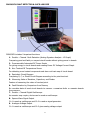
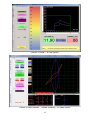
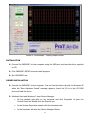
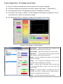
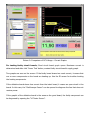
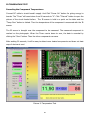
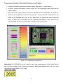
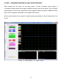
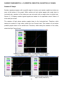
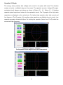
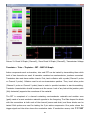
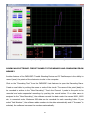
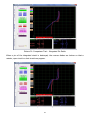
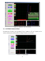
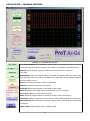
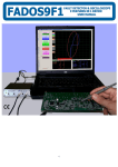
1 PRODUCT DESCRIPTION The Prot Ar - Ge Endüstriyel Proje Tasarım Teknolojik Ar - Ge Ltd. Şti. (Prot R&D Industrial Project Design R&D Ltd. Co.) FADOS9F1 Trouble Shooting & Oscilloscope Device is designed for trouble shooting all types of electronic boards. The FADOS9F1 is a PC-based VI Test Voltage – Current Analysis device. 2 unique capabilities are added to the FADOS9F1 over the FADOS7F1. The first feature is the Programmable DC Power Supply; thanks to the 0-16V and 20-1500mA adjustable power supply, the DC Voltage/Current graphs of the electronic board power supply can be produced. The second feature is the “IR Remote Temperature Measurement Sensor”; this sensor is used to find the components that heat up by drawing too much current. Using these two features together may reduce the time for trouble shooting some malfunctions by 5 to 10 times. These features can be used as a new technique for trouble shooting. Signature Analysis is a power-off test method that is used to troubleshoot circuit boards. FADOS9F1 works by applying a current-limited sine wave through a serial resistor point of touched on circuit and Voltage-Current (Signature) graph is displayed on the computer screen. In addition to these features, the computer software analyzes the Voltage – Current graph and shows the equivalent circuit diagram and the electronic components of the contact point. Those futures are intended to provide guidance to the user in order to facilitate trouble shooting. Using the Dual Channel VI test feature, the intact and defective (or suspect) electronic boards can be compared by touching the same points on each board at the same time, thus the out-oftolerance malfunctions can easily be diagnosed with this method. All the VI graphs are produced by the software making analyses at 720 separate points with an accuracy of 2.5 mV. Therefore the FADOS9F1 is very accurate. Memory Recording feature; by means of this feature, the characteristics of the intact electronic board ( VI graph, equivalent circuit diagram and electronic components values) are written on the computer’s hard disk and taking these points as reference, you can compare the defective (or assumed to be defective) electronic boards accurately, easily and rapidly. At the same time, the data can be written on the photograph of the board. Thus, the recorded point can be seen on the photograph while making a comparison from the memory. The software produces different sounds while comparing the matching and non-matching points during the test, thus allowing to concentrate only on the sound for a rapid comparison without 2 having to look at a board or display continuously. The user can compare the electronic boards from 3 different settings at the same time. (Selected Current-Voltage-Frequency steps) In addition to the above features, the VI FADOS9F1 Test Device can be used as a Dual-channel Oscilloscope, Square Wave Generator and Analog Voltage output. When the Square Wave Signal Output is used, a signal is applied to the electronic board and the other channels display the output signals on the oscilloscope screen. Technicians, engineers and hobbyists have found VI graph to be an effective and efficient method for troubleshooting printed circuit boards. The signature comparison method is easy to use and allows for immediate feedback that will assist you in locating faulty component. As you gain some experience with VI graph you will realize that FADOS9F1 is an indispensable troubleshooting tool. Usage is very easy and users will find the faults just by looking at graphs without comparison. When test Printed Circuit Assembly (PCA) with FADOS9F1, do not apply power to PCA. PCA and the devices must be made high-voltage capacitor discharges. There is no risk of further damage to the PCA while testing and troubleshooting. FADOS9F1 is easy to carry since it’s small. It can be carried in a laptop briefcase. Including many more features, it is like a Swiss knife of users dealing with electronics. Usage Areas ECU Automotive electronic circuit boards, servo-step motor drivers, circuit boards of medical devices, military electronic circuit boards, computer and monitor circuit boards, television-audioradio circuit boards, circuit boards of textile machines, mobile phone electronic circuit boards etc. (all type electronic circuit boards.) Electronic Components Test: Resistors, Capacitors, Inductors, Diodes (General purpose, Zener, High Voltage etc.) Transistors (NPN, PNP, JFET, MOSFET etc.), SCRs, TRIACs, Optocouplers, Integrated Circuits (Digital, Analog) etc. 3 Unique Features Integrated DC Power Source, IR (infrared) Sensor (Temperature Test), Equivalent Circuit Diagram and Measuring Values of all Components features are unique in the World. Integrated DC Power Source: It can be adjusted between 0-16V and 20-1500mA with power output. It gives energy to circuit boards and creating Power DC Voltage-Current Graph. IR (infrared) Sensor (Temperature Test): This feature is used for detecting more heated components and draw out heat map of electronic card. Equivalent circuit diagram and measuring values of all components features; as an example; if resistor connected parallel to capacitor, it shows circuit diagram and value of them at the same time. SECURITY 1- FADOS9F1 is produced by using lead-free solder and designed in accordance CE regulations; users must use the following usage rules. 2- Chassis must be isolated and grounded. Connect the chassis ground connection point of the probe is the same as your computer, careful to avoid the potential difference. 3- Feature of oscilloscope, if probe key is set to 1X, it measures ±12 Voltage, probe key is set to 10X, it measures ±100 Voltage. Do not use above these limits of voltage. 4- It tests electronic circuit boards without giving to energy. Before test, electronic circuit board and the devices must be made high-voltage capacitor discharges. 5- The users of this equipment must have knowledge and experience to repair of electronic circuit boards. Thus, during using FADOS9F1, do not make this mistakes such as touch chassis to high-voltage, non-isolated ground, test high-voltage capacitor discharges. Without enough knowledge and experience in this subject, keep away high voltages such as mains voltage which can damage the system and themselves. 6- Giving high-voltage from probes, series resistors which contained in the device damaged and makes the circuit an open circuit. In this case, the computer port which is connected device via USB port damaged but observed in other parts of the computer is not damaged. 4 FADOS9F1 PERFORMANS AND MEASURUMENT TOLERANCE 1- FADOS9F1 is designed multi-function as Voltage- Current (VI) Signature Analysis Tester and Oscilloscope. The main of the feature device is VI Tester; in addition to this feature, computer software by analyzing voltage-current graph to displays equivalent circuit diagram and values of electronic components in specific tolerances. The equivalent circuit diagram and values are for informational purposes. As the device is not suitable for direct measurement. And Computer software creates “Power Voltage-Current Graph” and measures temperature of components in specific tolerances. 2- Equivalent circuit diagram is drawing by software using mathematical functions and formulas; but rarely has the possibility of making mistake. This probability is more increased with applied externally electromagnetic fields of generated interference. The EMC Testing; 3V/M and the range of 80MHz-1GHz is approximately capacitor %1, resistor %3, diodes %1. Some fast diodes make oscillation in some frequencies, so that can be perceived as ‘active point’ by the device. VI Graph the rate of change: <1%. 3- Components Value Measurement Tolerance: Resistor: %2 Capacitor: %3 Diode Transmit Voltage: 0,1V If Resistor and Capacitor are connected Parallel: Resistor:%4, Capacitor: %5 If Resistor and Diodes are connected Serial: %4 If Diode and Resistor are connected Parallel: %3 If 2 Diodes and a Resistor are connected Parallel: %10 Note 1: These tolerances valid, if resistor curve makes angle between 10 and 80 degree to horizontal axis. If resistor curve close to horizontal line, select ‘Low Current’ Step and; if resistor curve close to vertical line, select ‘Middle or High Current’ Step for reducing mistake rate. Note 2: These tolerance valid, if capacitor ellipse of width/length ratio is greater than 1/4. This ratio is less than 1/4 and ellipse’s width - length is thin and long. In such a case; change current step or/and frequency step for selecting step appropriate to components. 4- Oscilloscope voltage measurement tolerance: %0,5. 5 PRODUCT OVERVIEW and CONTENT 1 FADOS9F1 Product 1 Software CD and User Manual (Pdf) 1 IR Temperature Probe 2 Oscilloscope Probes 1 Com Probe (Crocodile) 1 USB Cable 1 DC Cable 1 Power Adapter 1 Handbag Picture 1: FADOS9F1 Sets 6 FADOS9F1 TECHNICAL SPECIFICATIONS A- FAULT DETECTION SPECIFICATIONS: Test Voltages : ±1V, ±2V, ±6V, ±12V, ±24V Test Resistance : Current Level: Low 47KΩ, Med1 3,5KΩ, Med2 700Ω, High 250Ω Test Frequencies : Very Low Frequency :2 Hz Low2 Frequency :4 Hz Low1 Frequency : 12 Hz Test Frequency : 32.5 Hz High Frequency : 355.4 Hz Number of Channels : 2 (Channel 1 and Channel 2) Scan Mode : Manual or Automatic. Automatic selection steps of voltage, current, frequency. Other Feature : 1: Equivalent circuit diagram. 2: Resistor, capacitors, diodes etc measurement. 3: Data recording and comparing from memory. 4: Displaying 3 graphs of different settings at the same time. B- POWER – IR TEMPERATURE FEATURES: DC Power Supply : 0-16V 20-1500mA adjustable power output. IR (Infrared) Sensor : Measures the 0-120 degree differences according to the ambient temperature. C- PC OSCILLOSCOPE FEATURES: Sampling Rate : 400 K/S Input Voltage : Probe 1X: ±12 V Channel / ADC : 2 Channel / 12 Bit Accuracy : 2.5 mV Display speed : 0.02 mS/div….100 mS/div Momentary Memory : 64 Kbyte Probe 10X: ±100 V D- DIGITAL AND ANALOG OUTPUT: Output : Channel 2 Output Voltage : -12V….+12V (Adjustable) Frequency (Digital) : From 0.2KHz to 25KHz Dimensions : 122mm L x 113mm W x 29mm H Weight : 1100 gram with all accessories Table 1: FADOS9F1 Technical Features 7 CONTENTS Page PRODUCT DESCRIPTION ................................................................................. …….2 USAGE AREAS ............................................................................................................... 3 ELECTRONIC COMPONENTS TEST ....................................................................................... 3 UNIQUE FEATURES ......................................................................................................... 4 SECURITY ............................................................................................................... 4 FADOS9F1 PERFORMANS AND MEASURUMENT TOLERANCE ................................. 5 PRODUCT OVERVIEW AND CONTENT .................................................................... 6 FADOS9F1 TECHNICAL SPECIFICATIONS ............................................................... 7 FADOS9F1 FAULT DETECTOR & OSCILLOSCOPE ..................................................... 9 INSTALLATION - DRIVER INSTALLATION .............................................................................. 11 CONNECT PROBES ......................................................................................................... 12 GENERAL USAGE INFORMATION .......................................................................... 12 POWER – IR TEMPERATURE TEST ........................................................................ 14 POWER (SUPPLY) TEST – DC VOLTAGE – CURRENT GRAPH ..................................................... 16 COMPARISON OF THE POWER (SUPPLY) DC VI GRAPH WITH THE FAULTY BOARD’S DC VI GRAPH ..... 17 IR TEMPERATURE TEST ........................................................................................ 20 RECORDING THE COMPONENTS TEMPERATURES .................................................................... 20 TEMPERATURE CHECKS OF THE FAULTY ELECTRONIC CIRCUIT BOARD ......................................... 21 MICRO - VOLT ............................................................................................................. 21 VI TEST – PROGRAM FEATURES OF FAULT DETECTION PART .............................. 22 PASSIVE COMPONENTS R, L, C V/I GRAPH .......................................................... 23 RESISTOR VI GRAPH ..................................................................................................... 23 CAPACITOR VI GRAPH ................................................................................................... 25 CAPACITOR QUALITY TEST AND RC CIRCUIT ....................................................................... 26 SEMI CUNDOCTORS V/I GRAPH ........................................................................... 27 DIODE, ZENER DIODE VI GRAPH ...................................................................................... 27 TRANSISTOR – TRIAC – THYRISTOR – FET – IGBT VI GRAPH ................................................... 28 INTEGRATED CIRCUITS (ICs - SMD INTEGRATES) V/I GRAPH ............................ 30 SAVING AN ELECTRONIC CIRCUIT BOARD TO THE MEMORY AND COMPARISING FROM MEMORY..................................................................................................... 31 RECORDING THE TEST POINTS WITH IMAGE ........................................................................ 31 COMPARITIVE TEST OF THE COMPONENTS OF IN THE CIRCUIT BOARDS ........... 33 3G – 3 DIFFERENT GRAPHS DISPLAY ................................................................... 39 OSCILLOSCOPE – PROGRAM FEATURES ............................................................... 38 RECOMMENDATIONS............................................................................................ 42 WARRANTY AND CONDITIONS............................................................................. 43 8 FADOS9F1 FAULT DETECTOR & OSCILLOSCOPE Picture 2: FADOS9F1 FADOS9F1 includes 9 important functions: 1. Double – Channel Fault Detection (Analog Signature Analysis - VI Graph) Comparing good and faulty or suspect circuit boards without giving power to boards. 2. Programmable Integrated DC Power Supply For giving energy to circuit boards and creating Power DC Voltage-Current Graph. 3. Non Touched IR Temperature Sensor For detecting more heated components and draw out heat map of circuit board. 4. Equivalent Circuit Diagram Composing R, C, or Diode Circuit Diagram according to the point touched. 5. Measuring Value of Resistors, Capacitors, and Diodes Feature of measuring the value of touched point. 6. Fault Detection by Comparison from Memory By recording data of good circuit boards to memory, comparing faulty or suspects boards from memory. 7. Double – Channel Digital Oscilloscope As occasion may require, device can be used as oscilloscope. 8. Square Wave Signal Output Ch.1 is used as oscilloscope and Ch.2 is used as signal generator. 9. Analogue Voltage Output Ch.1 is used as oscilloscope and Ch.2 gives analog voltage output. 9 Picture 3: Power – IR Test Screen Picture 4: Fault Detector - Trouble Shooting – VI Tester Screen 10 Picture 5: Oscilloscope – Analog Output Screen INSTALLATION 1- Connect the FADOS9F1 to the computer using the USB port and load the driver supplied on CD. 2- Click FADOS9F1 SETUP.exe and install program. 3- Run FADOS9F1.exe DRIVER INSTALLATION 1- Connect the FADOS9F1 to the computer. You can load the driver directly for Windows XP when the “New Hardware Found” message appears. Insert the CD in to the CD ROM drive and load the driver. 2- Windows Vista and Windows 7 open Device Manager. On the desktop right-click on my computer and click Properties of open the Control Panel and double-click the System icon. In the System Properties window click the Hardware tab. In the Hardware tab click the Device Manager Button. 11 Or Click Start Click Settings Click Control Panel In the Control Panel double-click the Systems icon. In the System Properties window click the Hardware tab. In the Hardware tab click the Device Manager Button. 3- Find “Prot Ar-Ge FADOS9F1 Fault Detector” inside Universal Serial Bus Controllers and click right then, select “update software driver”. 4- Select (Search for the best driver location) and click browse, find FADOS9F1 Driver’s folder. 5- Click OK and install driver. Note: Each product has different calibration settings, so that please do not lost the FADOS9F1 program CD. CONNECT PROBES: Connect the DC Power Cable (Red-Black Cable) to the Power connector. Connect IR Sensor to IR Temp. connector. The Oscilloscope Probes and Com Probe (Crocodile) can be connected each VI Tester sockets. The probe with the yellow circle is always Channel 1; the probe with the blue circle is always Channel 2. The crocodile probe is always Com. USB cable is used for communication between the computer and FADOS9F1. Connect the Power Adaptor to the mains plug (18-20 VDC). GENERAL USAGE INFORMATION 1. When run software, Power – The IR Temperature Test screen opens and an input is entered to the VI Tester screen or Oscilloscope – Analog Output screen with the VI Tester button. While testing the Electronic boards, we recommend the user to use the Power – IR Temperature Test feature for testing. Firstly, create good circuit board’s “Power Voltage/Current Graph”. Than save this graph to memory. Compare faulty or suspect circuit boards 12 with good circuit board’s “Power Voltage/Current Graph”. If the faulty or suspect board draws too much current, it means that one or more components on the board are heating up. Use the IR sensor for trouble shooting the heating components. If the faulty (defective) board draws less current than the good (intact) board, it means an open circuit in the board. In this case, the “Oscilloscope Screen” can be opened to diagnose the line that does not receive power. If the graphic of the faulty (defective) board is the same as the good board, the faulty component can be diagnosed by opening the “VI Tester Screen”. 2. Open circuit’s graph is in the middle and horizontal position at Test-Fault Detect screen. Current – Voltage Graph (VI) makes angle according to the value of resistance, capacitor is like circle and ellipse, short circuit is vertical position. 3. In the Medium current mode, in the areas with high resistor values, if the VI graph is closer to the horizontal axis, you can see the resistors with high values more clearly by switching to low current. If the VI graph is too close to the vertical axis, this means that the resistor value is low and you can read the values more clearly by switching to the high current mode. 4. Please test the capacitors in the high frequency mode generally. Use low current when the capacitor value is low and high current if the value is large. If the capacitor value resembles a thin line in high current at the vertical axis, you can see the value more clearly by reducing the frequency from the frequency mode. 5. The pins of a good integrated circuit are generally in form of a dual reverse diode (other than the supply and ground). Although the attached resistors and/or capacitors might affect the graph, the two reverse diodes should be observed. In the output of some integrated circuit only one diode may also be seen. But an image in form of a resistor would most probably mean a defective integrated chip. 6. The capacity test shows the quality of the electrolytic capacitor in particular. The more horizontal this curve is, the higher the quality of the capacitor is. The angle of the deteriorating capacitor makes an angle with the horizontal. If the angle is large, it means a defective capacitor. Because the circuit draws a current while in the board, this test can be deceptive, hence consider this while testing. In case of doubt, remove the capacitor from the circuit and then measure; in this measurement, the test devices may show all of them as intact. The best capacitor quality measurements can be done by 13 looking at the “Capacity-Resistor Curve” with this product. While making this measurement, adjust the frequency and current to become longer on the vertical axis of the graph, but without forming a multiple and thin graph. 7. In case of a misshapen capacitor graph due to the effects of the diodes in the circuit, the value of the capacitor can be measured again after eliminating the effects of the diodes. 8. The important issue in trouble shooting is the shape of the graphs and their interpretation. Try to find the defects by comparing when starting. You should be able to distinguish the graphs of the good and defective materials in a short time. The Equivalent circuit diagram and values will aid you in the process. If you concentrate on the values in the equivalent circuit, diagnosing may take longer. Use the values of the components as necessary, but do not well on the values alone like the measurement logic of the test equipment. The evaluation logic of this product is based on the interpretation of the graphs, i.e. interpreting the graphs produced by the computer and generating the equivalent circuit diagram and showing the associated values. 14 POWER - IR TEMPERATURE TEST When you run the software; Power – IR Temperature Test screen pop-up. DC Voltage-Current Graph is seen at the screen. All control buttons are placed to the left of the panel used in Power – IR Test. Picture 6: Power – IR Test Screen 15 Power On : The FADOS9F1 DC provides an “Output” through the power cables. If the electronic board draws more current than the set value, the program limits the current and does not allow excessive current draw. Power Off : Cuts off the voltage. Power Test : Used to produce the “Current/Voltage Graph” of the electronic board’s power supply. Power : This option is for DC Power Test and measurement. Temperature : This option is for IR - Temperature Test and measurement. Micro Volt : This option is for Microvolt measurement. Low Current : Selected when measurement is made between 0-300 milliamp. Recording : Opens the file format and starts recording or opens a saved file. Temperature : Shows the Components’ Temperature values. Temp. Set : Shows the temperature of the component stored in the memory. Temp. Tol. ± : Shows Temperature Tolerance ±. User can change tolerance. Test Point : Shows the serial number of the point under test. Time : Shows “Counting down from 90 seconds.” Auto Test : If tolerance of test point is equal to tolerance mentioned below, the next data will be opened automatically. Next Point : Opens the next test point. Temp. Zero : Used for compensating the IR sensor for the room temperature. Voltage : Shows the Maximum Voltage. R : Shows the resistance of the circuit. Current (mA) : Shows the current drawn by the circuit. Bold Green Line : Shows the Component’s temperature value. Thin Green Lines : Shows Temp. Set ± Tolerance, for example; If Temp. Set is C, and Tolerance 2; green line sets between 16 C and 10 C. Power (Supply) Test – DC Voltage Current Graph 1. First the maximum Voltage and Current required by the board is adjusted. 2. The Power cables are connected to the board’s supply. Red Cable (+), Black cable (-). 3. The Voltage and Current are adjusted and power is supplied to the board. 4. The “Power Test” button is clicked. The DC Voltage-Current Graph is produced in 100 mV increments from 0 Volt to the maximum voltage. 5. The “Recording” button is clicked to record the DC Voltage-Current Graph. Picture 7: DC Voltage – Current Graph New Folder : Opens a new folder in the computer’s hard disk under the name given to a new circuit. Open Image : Open and upload the circuit of the image. New Point : If New Points is empty, software saves data with automatic number like and add to file. Power : If the DC Voltage/Current Graph is to be recorded, “Power” is selected. Temp. : If the components temperature value is to be recorded, Temp. (Temperature) is selected. Save : Saves the value of test point with mentioned name to the determined folder. If name is not given, saves with serial number. Change: To change the data of a recorded test point, the recorded test point is selected and the change button is pushed for changing the test point data. Open : The point selected is opened on the screen. Delete: Deletes the data of the marked point from the 17 computer. Comparison of the Power (Supply) DC VI Graph with the Faulty Board’s DC VI Graph Opening Recorded Data : Click “Recording Button” and select “Power Data”, then click on “Open Button” and to open the selected file. Picture 8: Recorded DC Voltage – Current Graph The DC VI graph of the good electronic board is opened from the memory. The Power cables are connected to the board’s supply. Red Cable (+), Black cable (-). The “Power Test” button is pushed to generate a DC VI graph of the faulty board. 18 Picture 9: Comparison of DC Voltage – Current Graphs For testing faulty circuit boards; Good circuit board graph opens. Maximum current is determined and after click ‘Power Test’ button, created faulty circuit board’s supply graph. Two graphs are seen on the screen. If the faulty board draws too much current, it means that one or more components on the board are heating up. Use the IR sensor for trouble shooting the heating components. If the defective board draws less current than the intact board, it means an open circuit in the board. In this case, the “Oscilloscope Screen” can be opened to diagnose the line that does not receive power. If the graphic of the defective board is the same as the good board, the faulty component can be diagnosed by opening the “VI Tester Screen”. 19 IR TEMPERATURE TEST Recording the Component Temperatures Connect DC cable to circuit board’s supply. And Click “Power On” button for giving energy to boards. The “Timer” will count down from 90 seconds to “0”. Click ““Record” button to open the picture of the circuit loaded before. The IR sensor is held to a point on the table and the “Temp Zero” button is clicked. Then the temperature of the component is measured with the IR sensor. The IR sensor is brought over the component to be measured. The measured component is marked on the photograph. When the Timer counts down to zero, the data is recorded by clicking the “Save” button. Then the other components can save. After waiting 90 seconds, it will be easy to detect more heated components and draw out heat map of electronic card. Picture 9: Temperature Test 20 Temperature Checks of the Faulty Electronic Circuit Board Connect the Power cables to the board’s supply. Red Cable (+), Black cable (-). Click the “Record (Recording)” button, select the “IR-Temperature Data” and click the “Open” button. Click the “Power Test” button and wait 90 seconds for the components to warm up. Measure the temperature of the first component. If the measured temperature is the same as the recorded data, click on the “Next Point” to opened the second recorded data. If “Auto Test” is selected and the measured temperature is the same as the recorded data, the other recorded data is opened a few seconds later. Picture 10: Temperature Comparison Micro-Volt: The FADOS9F1 can be used for micro volt measurements. Select Micro-Volt to open the Micro Voltage screen. Connect one probe to IR plug and measure micro volt. It is used for measure voltage below 2,5 µV. max. 21 VI TEST – PROGRAM FEATURES OF FAULT DETECTION PART While testing with V/I graph, do not apply power to board. Generally, probe chassis is connected to board chassis and a signal is applied to touch point by the device. The V/I graphic signal appears on the screen. Signals scans from negative voltage to positive voltage and when open circuit, it appears horizontally in the middle of the screen. All the control buttons to be used for trouble shooting are placed on the left hand side of the screen. Picture 11: Fault Detector – VI Tester Screen 22 Channel: Used to select channel. Auto: When this setting is selected, the most suitable value of the Voltage, Frequency and Current levels are shown on the screen depending on the characteristics of the contact point. Voltage Step: The voltage to be applied to the board is selected by manually selecting out of the ±1 V, ±2 V, ± V, ±12 V, ±24 V voltage levels. One voltage level only can be selected for a test. Frequency Step: The frequency to be applied to the board is selected by manually selecting out of the Multi Low Frequency, Low 2 Frequency, Low 1 Frequency, Test Frequency, High Frequency levels. One frequency level only can be selected for a test. Current Step: The current to be applied to the board is selected by manually selecting out of the Low Current, Medium1 Current, Medium2 Current, High Current levels. One current level only can be selected for a test. Comparison: If this option is selected, good (solid) and faulty or suspect circuit boards are compared by touching probes to the same points of both circuit board. Capacitor Test: Capacitor test determines quality of electrolytic capacitor. TTT FET IGBT: If this option is selected, determines TTT, FET, IGBT etc. Type of semi – conductors. Recording: Opens the file format and starts recording or opens a saved file. Grf: Allows selecting graphs in 3 different settings (voltage – frequency – current) and switching rapidly. 1G, 2G, 3G: Graphs in 1, 2 or 3 different settings can be displayed on the screen at the same time. simultaneously. Recording: Opens the file format and starts recording or opens a saved file. Test Point: Shows the serial number of the Test point. Point: Shows the name or code of the Test point. : Opens the previous test point. : Opens the next test point. Reference: Channel1 indicates good (solid) circuit; Channel2 indicates faulty circuit or circuit to be tested. When saved at memory, Reference=Channel1 is saved. Values of circuits composed of resistance, capacitor, and diode are displayed. 23 PASSIVE COMPONENTS R, L, C (RESISTOR, INDUCTOR, CAPACITOR) V/I GRAPH Resistor VI Graph Resistor signatures appear with a specific angle to horizon; and resistor symbol and value are seen at the bottom of the graph. While resistors at high values appear with angle close to horizontal axis, resistors at low values are seen at screen with an angle close to vertical axis. Picture 12, 13 display resistors typical signals and values for the equivalent circuit. Picture 14 short and open circuit. The resistors of high values produce graphs closer to the horizontal axis. Therefore, while testing the resistors of high value, select the Low Current Level. The resistors of low values produce graphs closer to the vertical axis. Therefore, while testing the resistors of low value, select the High Current Level. Picture 12: Resistors VI Graphs, The Equivalent Circuit Diagram and Value Measurement (Channel 1 Red - Channel 2 Blue) Picture 13: Resistors VI Graphs Picture 14: Short Circuit (Channel 1) and Open Circuit (Channel 2) 24 Capacitor VI Graph The energy storing devices leak voltage and current in the phase shift area. This situation creates a circular or elliptical shape on the screen. The capacitor current / voltage (VI) graph, equivalent circuit diagram and values are shown in Picture 15 - 16. Picture 15 - 16 displays capacitor typical signals and values for the equivalent circuit. The VI graphs of the high value capacitors are displayed on the vertical axis. For testing high capacitor select high current and low frequency. The VI graphs of the medium value capacitors are elliptical close to a circle. Low capacitor generates horizontal ellipse. For testing low capacitor (lower than 10 nF) select low current and high frequency. Picture 15: Capacitor VI Graph, The Equivalent Circuit diagram and Value Measurement Picture 16: Capacitor VI Graph 25 Capacitor Quality Test and RC Circuit When “Capacitor Test” is selected, an additional curve displaying the quality of capacitor appears. If this curve is at horizontal axis or close to it, quality is high; and quality is low as much as the angle degree is high. High quality capacitor generates a horizontal line. Picture 17: High Quality Capacitor Picture 18: Low Quality Capacitor Picture 19: Capacitor and RC Circuit The axis of the graphs for the RC circuits comprising Resistors and Capacitors makes an angle. 26 SEMI CONDUCTORS VI GRAPH Diode – Zener Diode VI Graph Diodes start to transmit current after high transmission voltage. For this reason, diodes are seen horizontally at one part of the graph, and are seen vertically at the other part. If cathode of diode is connected to chassis, a curve appears at horizontal axis at negative voltage and before transmits voltage; and the curve appears at vertical axis at transmit voltage. If anode of diode is at chassis, a curve appears to down at negative voltage. A Zener diode exhibits the same signature as a conventional diode for voltages below the Zener voltage. When the reverse bias exceeds the Zener voltage, a low resistance signature is displayed. If diode and resistor are serial on circuit, after transmission, graph makes an angle to horizon. Picture 20: Diode and Serial Diode - Resistor VI Graph, The Equivalent Circuit Diagram 27 Picture 21: Diode VI Graph (Channel1), Zener Diode VI Graph (Channel2), Transmission Voltage Transistor – Triac – Thyristor – FET - IGBT VI Graph Active components such as transistor, triac and FET can be tested by transmitting them while both of two channels are used. A transistor contains two semiconductor junctions connected. Transistors also must have emitter chassis. First, touch collector with a probe (Channel 1 probe or Channel 2 probe). Collector must be at non-transmission position. Then, touch other probe (Channel 1 probe or Channel 2 probe) base in order to provide transistor to start transmitting. Transistor characteristics should be seen as at the screen. Lack of any leak at the junction point (fully horizontal) supports the soundness of the material. The FET is comprised of a channel containing semi-conductor materials and another zone (gate) made of a semi-conductor material opposite to the foregoing. The Gate shapes the diode with the connections at both ends of the channel (source and drain) and those diodes can be tested. Both probes are used for testing the 3-pin active components. One probe shows the trigger signal and the other shows the conduction state. If conduction occurs; click T.T.T FET 28 IGTB from the test types menu and the software checks if the FET – MOSFET is of the N or P type. MOSFET are field effect transistors. Gate - drain and gate - source tests generally yield an open circuit mark. However, some MOSFETs have a protective diode between the gate and source. In such cases, the gate-source marking is similar to a zener diode. Those are checked like the FET using the source - drain conduction and gate - source voltage. The MOSFETs on the other hand are checked by means of the normal and reverse polarization of the gate-source junction. Triac, Thyristor, IGBT can be tested in the same way. If Thyristor,Triac, Transistor, FET, IGBT selection (T.T.T FET IGBT button) is applied, type of component can be determined. Picture 22: NPN Transistor Picture 23: PNP Transistor Picture 24: N FET Picture 25: P FET 29 INTEGRATED CIRCUITS (ICs – SMD INTEGRATES) Integrated circuits can be tested all the pins with the help of probes. Circuits made up of many components encapsulated within a single package. The component count within an IC may vary from as few as half a dozen devices on a "chip" to many thousands of components in, for instance, a modern microprocessor. Because of the need to package so many components into an extremely small space, components within an IC are often microscopically small. As a result, modern ICs contain components and connections which are susceptible to damage from electrical stress and static discharge at levels far lower than those which would damage normal components. For this reason, many ICs incorporate protection diodes on their signal input and output pins. When testing integrates signals display similar to the double-inverse diode, zener diode and diodes. It can be capacitors or resistors are connected to these. If pin of integrated has double reverse diode, it means this pin can be good. We can use the same technique to locate faults in ICs which are large and very complex, such as memory chips and microprocessors. The pin arrangement of such complex ICs means that it is especially appropriate to use comparison techniques to test these devices. As we look at these devices we will find that, despite the large number of pins, there are only a few distinct graph patterns on a digital IC. Note: You will frequently notice differences in the signatures between similar ICs from different vendors or which have been manufactured using different technologies. Compare the graph on a suspect pin with graphs from other pins on the same device before regarding the device as faulty. 30 Picture 26: Good (Solid) Integrated Pins – Compare 2 Integrated Pins SAVING AN ELECTRONIC CIRCUIT BOARD TO THE MEMORY AND COMPARING FROM MEMORY Another feature of the FADOS9F1 Trouble Shooting Device and PC Oscilloscope is the ability to record (save) the points of the electronic circuits in the computer. Click on the “Recording Test” from the FADOS9F1 test features to open the Recording Menu. Create a new folder by writing the name or code of the circuit. The name of the point (data) to be recorded is written in the “New Recording”. Touch the Channel 1 probe to the point to be recorded and make sequential recordings by pushing the record button. If no data name is assigned to the “New Recording”, the software records the data under the names N001, N002 etc. in numerical order. Maximum 999 data can be recorded for each recording folder. If you select “Add Number”, the software adds numbers to the data automatically and if “Increase” is selected, the software increases the numbers automatically. 31 In order to test from saved file, press “record memorized test” button, select data to be tested and open first saved point. Saved data is seen as a red graph at first channel. Touch the point to be tested with second channel. If it is same as the saved data or in tolerance values, it is written “Harmonious” at screen. If it is out of tolerance values, it is written “Disharmony”, percentage value is seen and wrong voice is heard. When automatic test is activated, if a test point is harmonious, then it goes to next point automatically. This feature allows rapid testing without having to look at the monitor. Note: The test points of the Electronic may be recorded only with Channel 1. The test points saved with the Recording Menu can be opened as reference and the points on the defective circuit can be compared with those using Channel 2. New Folder: Opens a folder on the computer’s hard disk for a new circuit with a given name. Open Image: Open and upload the circuit of the image. New Point: The name of the point to be recorded is written; if left blank, the software adds the numbers “N001, N002” etc. to the file automatically. Add Number: Adds a number to the test points automatically. Inc.: Increments the numbers automatically. Save: Saves the value of the test point to the file specified with a given name. Change: In order to change the data of a saved test point, select the saved test point and click on the “Change” button” to change the saved data. Open: Opens the data for the marked test point as reference o Channel 1. Delete: Deletes the data for the marked test point from the computer. Recording The Test Points With Image Open a new folder for the board to be recorded. Click on “Load Figure” to select the photograph of the circuit from the window opened. The software changes the name of the photograph to “image” automatically. For example, if the name of the photograph is “Figure.jpg”, the software changes the name of the photograph to “image.jpg” automatically and adds to the file. If you want to add a photograph to the folder, you need to change the name of the photograph as “image.jpg” since the software checks the files named “image.jpg” 32 only. If the name is not written as “image.jpg”, this feature will not work. After loading the figure, a photograph of the circuit is shown at the lower right corner of the VI test screen. The green buttons on the photograph for “+”,”-“zooming. Select the point to be recorded on the photograph, then touch the Channel 1 probe to that point and push the “Record” (Save) button. When you use this feature for comparing from the memory, you can see the location of the saved point on the board. Picture 27: Recording Data with Image COMPARATIVE TEST OF THE COMPONENTS IN THE CIRCUITS BOARDS When a component is tested in the circuit, the other parallel or serial components in the circuit cause a mixed signal to be generated. The FADOS9F1 displays the mixed signals of the components on the electronic board and produces an equivalent circuit diagram to measure and compare the values of the components. You can perform the test by connecting the card assumed to be good to Channel 1 and the suspect circuit to Channel 2 from the common points. Comparisons can be made starting from the power supply to the board and progressing inputs and other suspected points. If it is same 33 as, it is written “Harmonious” at screen. If it is out of tolerance values, it is written “Disharmony”, percentage value is seen and wrong voice is heard. Picture 28: Comparison Test Comparing this system is very sensitive and is considered compatible with the values within the given tolerance. 34 Picture 29: Comparison Test In this system, multiple accurate comparisons are made and the values falling within the tolerances specified are considered as compatible. But, in case of small differences, determining is defective or not is left to the experience of the user. An important difference to be observed in Picture 29 is the difference of the resistor’s value in the test circuit. This is caused by the integrated circuits with reverse diodes. The integrated circuits usually contain reverse diodes. There may be capacitors and resistors connected as well. If there is a dual reverse diode connected to the pin of the integrated circuit, it can be said that this pin is intact. In particular, if there is complete matching in the comparison, 35 this point should be good. Picture 30: Comparison Test Integrated circuit is usually double reverse diode. It can be capacitors or resistors are connected to these. If pin of integrated has double reverse diode, it means this pin can be good (solid). 36 Picture 31: Comparison Test – Integrated Pin Faults When a pin of the integrated circuit is destroyed, the reverse diodes are broken so that a resistor, open circuit or short circuit may appear. Picture 32: Comparison Test – Integrated Pin Faults 37 Picture 33: Comparison Test – Parallel Resistor Faults An important difference to be observed in Picture 33 is the missing resistor in the reference circuit. This may result from a broken trace leading to the resistor or a cold solder at the resistor lead. The reverse diodes are caused by the integrated circuit. 38 Picture 34: Comparison Test From Memory 3G - 3 DIFFERENT GRAPHS DISPLAY By pushing the 1G button, you can display 2G (e.g. 2 graphs) or 3G (e.g. 3 graphs) on the monitor simultaneously selecting different voltage, frequency, current levels. Picture 35: 3G Graph Display 39 Picture 36: 3G Graph Display In Picture 36, the 3G feature has been used to set Voltage Level 12V, Frequency Level Test Frequency, Current levels Low Current, Medium 1 Current and Medium 2 Current. As can be seen from the example, a component that does not show any defect with Low Current proves to be defective when Medium Current 1 is used. 40 OSCILLOSCOPE – PROGRAM FEATURES Picture 37: Oscilloscope Screen Osc. Active/Passive: The Oscilloscope button makes the Oscilloscope active or freezes the current image and saves the image to the memory by pushing the recording button. Channel: Selects channel. Channel1, Channel2 and both channels are selected in an order. Manual/Auto: When the Manual setting is selected, the signals within the Lower Limit (mV) and Upper Limit (mV) values are captured. On Automatic, the last signal is captured when the signal is cut off. Save: Saves oscilloscope data or opens recorded data. Channel: Channel is selected for synchronous. Up/Down: Starts synchronization at the rising or falling edge. Probe X1: Adjusts the voltage value of the probe by the X1 or X10 level. Top or Low: Highest or lowest value on screen. Point: Shows the voltage value at a vertical line to the cursor in the memory. Frequency: Shows the frequency, if the frequency of the incoming signal can be detected. Active/Passive: When this button is clicked, a square wave or analog output is generated at Channel 2. Signal / DAC: Selects Square wave or analog voltage. 41 Frequency: Determines the frequency of the Square wave signal output. Voltage: Determines the voltage of the Square wave or analog output. Voltage Display Sensitivity: (Voltage/Division) Adjusts the voltage display sensitivity. The accuracy of the data received from the product does not change. The figures show the voltage value. If the figures are double clicked, the “0 V” reference of the channel is taken as the point clicked. Data received from device is 12 Bit, 2.5mV sensitive. Zero Adjustment: Shifts the ‘0 V’ point of the image upwards or downwards. The figures show the voltage value. If the figures are double clicked, the “0 V” reference of the channel is starts the point clicked. Starting Point:: Sets the starting point of the displayed section of the image in the “Memory” mode. ‘ Time Adjustment: Time/Division. Adjusts the time allocated to each division on the horizontal axis (time axis). RECOMMENDATIONS 1. The probes should be set to 1X while trouble shooting (fault detection). 2. Test good (solid) circuit board channel 1, faulty or suspect circuit board channel 2. First touch the channel 1 probe, and then touch channel 2 probes. 3. The important aspect in trouble shooting is the matching of the graphs. The lower circuit diagram and values are for assistance purposes. The values in the circuit diagram are not for measurement but for comparison. Wrong indications may be given with the effects of the other components on the board. 4. While using the device, testing at the medium current level is recommended. When necessary, use the low current level (i.e. high value resistors or low value capacitors). 5. When recording in the memory, click save button after touching good (solid) circuit board’s pins with channel 1. When the data open from memory, using Channel 2 comparison data with faulty, suspect or good (solid) circuit board. 6. In the Oscilloscope mode, the 1X setting of the probe measures up to 5V, and the 10X setting up to 50 volts. Measuring high voltage circuits is not recommended. 7. Each product has different calibration settings. The calibration file can be found on the CD in the program installation folder. Please do not lose the program CD. 42 WARRANTY AND CONDITIONS 1. The warranty period is 1 year from the date of product delivery. 2. The repair period is seven (7) business days. 3. Any defects arising out of not using the product in conformity with the instruction manual are not covered by the warranty. If a higher voltage than the voltage values specified for the probes is used, the series resistors connected to the probes burn out. The burning of the resistors shows a user error because of not discharging the high voltage capacitors before use, hence such conditions are excluded from the warranty. 4. The device is in a solid box. Normally use, the card is not physically damaged. The device is in an aluminum case, therefore the electronic board cannot be damaged physically. Breaking, wetting etc. are not covered by warranty. 5. The probes may be damaged depending on use. Therefore the probe malfunctions are not covered by the warranty. 6. In case of device failure, send the device to an authorized repair service or Prot Ar-Ge Company. 43


![View User`s Manual [US] - Acoustic Amplification](http://vs1.manualzilla.com/store/data/005687953_1-09ed6117760df16c9056fa1c8c49b775-150x150.png)