1
FADC System
Belle SVD 2.0 readout
Programmer’s Manual
V0.93 • 23 June 2003
BELLE
HEPHYVIENNA
DISCLAIMER
The FADCTF is a complex electronic system which can be
damaged if handled improperly. In particular, the following
guidelines must be respected by the operator. We decline any
responsibility for errors, damage or injury resulting from such
misuse.
• Crate and modules belong together.
Do not use the VME modules (FADCTF, Sequencer, PCI-Link) in
a VME crate other than the one provided with the system.
The user defined ±V1 and ±V2 rails are used to supply special voltages to
the FADCTF modules; while the Sequencer board provides ±12V which is
required by the Sparc interface. Moreover, the FADCTF modules are
mechanically coded with the corresponding counterparts in the crate.
• Always power off to change modules.
Never remove or insert a VME module of the system when the
crate power is on. Ensure that each module is fully inserted
(needs some force).
The VME interface Altera (EPM7256S; 5V core) is not specified for hotswapping. It can take damage by contention between logic levels and power
supply during plugging of the module or in case of bad contact.
• Double-check the VME base addresses.
It is extremely important that each FADCTF module has the
correct VME base address set.
Altera programming and I/O interfacing to neighboring modules as used by
the L0 trigger processor rely on the correct VME base address setting
which corresponds to the mechanical coding. If the address is wrong and
outputs of two modules are connected, both modules will be damaged by
overheating.
• Do not use the JTAG feature.
Programming Altera devices on the FADCTF modules is for
experts only.
All Altera devices (except for the VME protocol interface) can be
programmed by the JTAG bus that is accessible by VME. Obviously, much
harm can be done by improper use of this feature. The worst case is to blow
up all Altera devices on the board.
2
Table of Contents
1
2
Contact .......................................5
Overview ......................................5
2.1 Power on ......................................... 5
2.1.1
2.1.2
2.1.3
Load Altera chips............................... 5
Select clock source............................ 5
Reset FADCTF .................................. 6
2.2 Modes of operation............................ 6
2.2.1
2.2.2
mode)
2.2.3
Normal data taking ............................ 6
External test mode (nibble or transparent
6
Internal test mode ............................. 6
2.3 VME implementation.......................... 7
2.4 VME command notation ..................... 7
3
Addresses and coding ....................8
3.1 VME base addresses ......................... 8
3.2 Mechanical coding ............................. 9
3.2.1
3.2.2
4
Crates ............................................. 9
FADCTF modules............................... 9
FADCTF .....................................11
4.1 Address space ................................ 11
4.2 Bus systems .................................. 11
4.2.1
4.2.2
Overview ........................................ 11
Local Bus 1 — (A17…A21)=0 ................. 12
4.2.2.1
Timing Control – TIP1 ......................... 14
4.2.2.1.1 Event number and DAP/Final Memory ............. 14
4.2.2.1.2 Fast-Or counter, ext. test mode, start, test
pulse
14
4.2.2.2
Signal Processing – DAPx .................... 15
4.2.2.2.1
4.2.2.2.2
4.2.2.2.3
4.2.2.2.4
Read ADC event buffer FIFOs......................... 15
Read/Write Pedestal+Threshold memory......... 15
Read Fast-Or trigger counters....................... 15
Read hitmap L1.5 data .................................. 16
3
4.2.2.3
4.2.3
Simple L1.5 processor ....................... 16
Local Bus 2 — A21=A01=1, (A20…A02)=0 .. 16
4.2.3.1
Final Memory .................................... 16
4.2.4
Serial Bus 1 — L0 (A21…A19)=0, A18=1 and
(A17…A03)=0 ................................................. 17
4.2.4.1
4.2.4.2
Enable/reset L0 counters.................... 17
Read L0 counters .............................. 18
4.2.4.2.1 Read straight L0 counter .............................. 18
4.2.4.2.2 Read VME system clock gated L0 counter ...... 18
4.2.4.3
Module interconnection links ................ 18
4.2.5
Serial
Bus
2
—
DAQ
(A21…A20)=0,
(A19…A18)=1 and (A17…A01)=0............................. 18
5
Sequencer ..................................21
5.1 Address Space ............................... 21
5.2 General functions ............................ 21
5.2.1
5.2.2
Reset, TTM or standalone ................ 21
Clock source................................... 22
5.3 TTM L1.5 accept ............................ 22
5.4 Standalone test functions ................ 23
5.4.1
5.4.2
5.4.3
Normal readout cycle(s) .................... 23
Simulate external test mode.............. 23
4-channel analog test output (RJ45)... 23
5.4.3.1
5.4.3.2
Automatic DAC ramp ......................... 23
Set static DAC value .......................... 24
5.5 PCI-Link test input .......................... 24
5.5.1
status
5.5.2
5.5.3
Read XREQUEST, BUSY and trigger
24
Set PCI-Link XENABLE and XREADY... 24
Read PCI-Link data ........................... 24
4
1 Contact
The FADC system is designed, built and maintained by
Institute of High Energy Physics
Austrian Academy of Sciences
Nikolsdorfergasse 18
A-1050 Vienna
Austria
Phone: +43-1-5447328-0
Fax: +43-1-5447328-54
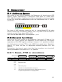
2 Overview
This document describes the VME connectivity of the FADC system
components. Please refer to the FADCTF User’s Manual for an introduction
to the FADCTF system hardware.
The VME base address of the Sequencer module is called S_BASE, and the
base address of one FADCTF module is F_BASE.
2.1 Power on
2.1.1 Load Altera chips
When the crate power is switched on, the Altera chips are loaded from
EEPROMs or flash memories. However, the supply voltages may still ramp up
and thus may cause errors during the loading process. Thus, it is
recommended to re-load the Altera chips on the FADCTF boards by the two
VME commands
FADCTF
F_BASE+0x2c0000 D00=1
start Altera loading
(wait >50µs)
FADCTF
F_BASE+0x2c0000
D00=0
stop Altera loading
The actual loading process will take a few seconds, during which no VME
commands shall be issued.
2.1.2 Select clock source
Most of the logic units on the FADCTF will need a clock for proper
functioning. Thus, before sending any further VME commands, the clock
source should be set in the Sequencer. Its default condition after power-on
is to transparently repeat all TTM signals including the clock. However, it is
recommended to reset the Sequencer and set the desired clock source by
VME:
Seq
S_BASE+0x00
D30=1
Sequencer FIFO reset (clear)
Seq
S_BASE+0x00
D31=1
Sequencer reset (see 5.2.1, p. 21)
Seq
S_BASE+0x08
D00=ttm
TTM or ext. clock (see 5.2.2, p. 22)
5
Seq
S_BASE+0x0c
D00=q
ext. or quartz clock (see 5.2.2, p. 22)
NB: The switch on the Sequencer front panel has be be in „INT“ (left) position
and internal mode (see 5.2.1, p. 21) has to be selected to enable the
internal quartz clock. The TTM clock can only be chosen in external mode
(power-on default), while the front panel input clock is selectable regardless
of switch or mode.
2.1.3 Reset FADCTF
Although the FADCTF should be in normal data taking mode by default after
power-on, it is recommended to send a general reset by VME which definitely
sets it to that state:
FADCTF
F_BASE+0x3c0000
D31…00=x FADCTF reset (see 4.2.1, p. 11)
NB: The reset signal is issued by any write operation to this VME address
regardless of the data bits.
2.2 Modes of operation
After everything is properly initialized, the user must decide in which mode
the FADCTF shall be put. In the final environment of the FADC system, there
will be 3 different modes of operation described below.
2.2.1 Normal data taking
The normal data acquisition under the control of the TTM system and with
PCI-Link output is the default condition after power-on or after a general
reset (GENRES). Thus, no more settings are required.
2.2.2 External test mode
transparent mode)
(nibble
or
Each VA1TA will present one channel in transparent mode that is digitized
and read out by the FADC system. This mode requires clock, start and ADC
clock signals from the TTM system (EFT should be low). The following VME
registers are linked to the external test mode:
FADCTF
F_BASE+0x018800
D02=1
external test mode (see 4.2.2.1.2, p. 14)
FADCTF
F_BASE+DAPx
D01=0|1
5 or 20MHz (see 4.2.2.2.3, p. 15)
NB: The sample taking clock has to be set for each DAP unit (addresses:
DAP 2 / 3 / 4 = 0x001000 / 0x002000 / 0x003000,
DAP 5 / 6 / 7 = 0x005000 / 0x006000 / 0x007000 ).
2.2.3 Internal test mode
This mode is used to find potential errors within a module or a crate and
does not require TTM system or the PCI-Link. Instead, one can use VME
commands on the Sequencer to create the necessary input signals. First of
all, the Sequencer must be set into the internal test mode (requires the
front panel switch in “INT” (left) position):
Seq
S_BASE+0x00
D00=1
Sequencer internal mode (see 5.2.1, p. 21)
The signals for a readout cycle can be generated by the Sequencer using
6
Seq
S_BASE+0x04
D00=1
Generate readout cycle (see 5.4.1, p. 23)
NB: There are additional options for the readout cycle which are described in
chapter 5.4.1, p. 23.
2.3 VME implementation
Many registers allow write and read operations, but in most cases these
functions are not accessing the same registers. Thus, writable registers
usually cannot be read back (except for the TIP1_B register in the Timing
Control Unit of the FADCTF).
We are sorry that the VME implementation is a bit confusing and not really
intuitive, because it is historically grown. During the development, features
were added continuously, but we refrain from re-designing the protocol since
this would have large implications on existing software.
2.4 VME command notation
The VME commands shown here are in the National Instruments CVI
notation, which consists of the write command
VXIout(type,address,bytes,data)
and the similar read command
VXIin(type,address,bytes,&data)
The first argument specifies the type of VME transfer (address modifier),
followed by the address (up to 32 bits), the number of bytes to be
transferred (1, 2 or 4) and the data word (up to 32 bits) to be written or
read. With this knowledge, the input/output functions can be easily
translated to match the requirements of other systems (such as the Sparc
CPU).
All surrounding code is written in plain C language.
7
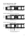
3 Addresses and coding
3.1 VME base addresses
Each VME module will get its own A32 address space. Basically, the
numbering scheme will follow the slot numbers for what concerns the
Sequencer and the FADCTF modules. Moreover, we have to distinguish two
crates (rϕ and rz).
Crate
VME base address bits A31…A24
rϕ
Slot number
rz
Slot number + 0x20
FADCTF
4
5
6
7
8
9
10
11
12
13
14
15
16
17
18
19
20
21
VME
Crate
Slots
1
2
6U
VME base addr.
(bits A31...A24)
3
P3 backplane
P2 backplane
ADC_PCI-Link
FADCTF
ADC_PCI-Link
FADCTF
ADC_PCI-Link
FADCTF
ADC_PCI-Link
FADCTF
ADC_PCI-Link
FADCTF
ADC_PCI-Link
FADCTF
17
R
ADC_PCI-Link
FADCTF
16
M
ADC_PCI-Link
FADCTF
15
L
ADC_PCI-Link
FADCTF
14
R
ADC_PCI-Link
FADCTF
13
M
ADC_PCI-Link
12
L
ADC_PCI-Link
11
R
FADCTF
10
M
ADC_PCI-Link
9
L
FADCTF
8
R
ADC_PCI-Link
7
M
FADCTF
6
L
ADC_PCI-Link
5
R
FADCTF
4
M
ADC_PCI-Link
3
L
FADCTF
2
R
ADC_PCI-Link
1
M
FADCTF
0
L
ADC_PCI-Link
Sequencer
Sparc CPU
Segment number
3-segment groups
FADCTF
Since the Sequencer must be inserted in slot 3, it will have the base
address 0x03000000 in the rϕ crate and 0x23000000 in the rz crate. The
illustration below gives an overview of all base addresses.
9U
rϕ crate 0x03 0x04 0x05 0x06 0x07 0x08 0x09 0x0A 0x0B 0x0C 0x0D 0x0E 0x0F 0x10 0x11 0x12 0x13 0x14 0x15
rz crate 0x23 0x24 0x25 0x26 0x27 0x28 0x29 0x2A 0x2B 0x2C 0x2D 0x2E 0x2F 0x30 0x31 0x32 0x33 0x34 0x35
8
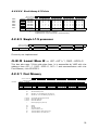
3.2 Mechanical coding
3.2.1 Crates
Slot
L
M
R
L
4
5
6
7
rϕ crate
Mechanical coding has been introduced to prevent the modules from wrong
insertion. The reason for this are the L0 (and optionally L1.5) trigger
processor interconnections: Two output buses must not be connected
together or the Altera chips will take damage from overheating.
Plastic pins are inserted at each slot of the crate (3 at bottom and 3 on
top) and on the counterpart of the FADCTF modules. By this method, a
module can only be inserted in a matching slot.
In total, there are 6 different L0 firmware versions: One for Left, Middle and
Right modules each in rϕ and rz crates. This is reflected by 6 different
mechanical codings as shown below. With equal codes for top an bottom pins
for each slot, one (mechanically equal) red pin indicates is detached at left,
middle or right position to indicate the type of module. Module (or segment)
triplets are equal, and so is the mechanical coding, which is identical e.g. for
slots 4,7,10,13,16,19 as well as the L0 processor.
The code pins are oriented horizontally and vertically in rϕ and rz crates,
respectively.
Slot
L
M
R
L
4
5
6
7
rz crate
Crate coding shown here (front view)
IMPORTANT: The pin coding in the VME crates must never be
removed since it prevents wrong insertion of modules which can
damage the L0 processor Altera. We decline any responsibility for
the consequences of such action.
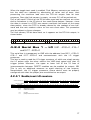
3.2.2 FADCTF modules
The FADCTF modules are be equipped with pins that match the crate coding.
All valid combinations of slot number, coding, module type and VME base
address are shown in the table below. NB: The codes are shown when looking
from the rear (VME connector side) towards the back of the FADCTF front
panel.
9
Crate
Coding
(rear view)
rϕ crate
VME base
address
4
7
10
13
16
19
5
8
11
14
17
20
0x04
0x07
0x0a
0x0d
0x10
0x13
0x05
0x08
0x0b
0x0e
0x11
0x14
R
6
9
12
15
18
21
0x06
0x09
0x0c
0x0f
0x12
0x15
L
4
7
10
13
16
19
0x24
0x27
0x2a
0x2d
0x30
0x33
M
5
8
11
14
17
20
0x25
0x28
0x2b
0x2e
0x31
0x34
R
6
9
12
15
18
21
0x26
0x29
0x2c
0x2f
0x32
0x35
L
rz crate
Slot
M
10
4 FADCTF
4.1 Address space
Each module within a crate will have its own A32 address space
representing a contiguous data block of 16MB (bits A23…A0).
Bits A31…A24 of the base address can be selected by two switches which
are located close to the rear end of the PCB between The VME connectors
P1 and P2. Each switch provides a range of 0x0…0xF, resulting in a total
space of 256 different addresses. Switch SW2 serves the highest 4 bits,
while SW1 sets bits A27…A24, as indicated in the drawing below.
A32 address bits
31 30 29 28 27 26 25 24 23 22 21
SW2
SW1
2
1
BR
The address bits A23 and A22 are reserved for the broadcast mode. If these
bits are both set, every FADCTF module reacts regardless of address bits
A31…A24. This is useful e.g. to generate a global, synchronous test pulse
or to globally turn on/off the Fast-Or counters.
Let’s call a module’s base address F_BASE. All VME addresses in the tables
within this document are shown in HEX format.
4.2 Bus systems
4.2.1 Overview
A FADCTF module has a total number of 7 internal buses which are all
accessible by VME.
• 2 parallel buses (Local Bus 1 and 2)
• 2 serial buses (DAC and L0 processor)
• 3 JTAG buses
These bus systems and their VME connectivity will be described in detail
below.
A general reset (RES) issued by VME affects the parallel buses 1 and 2 and
puts the module into a state ready for normal data taking; i.e. all registers
are set for that purpose.
The VME addresses (relative to F_BASE) of the individual buses are shown in
the table below.
11
Bus
VME address Description
(rel to F_BASE)
Local Bus 1
0x000000
Data Processors, Timing Control, L1.5 Proc.
Local Bus 2
0x020000
Final Memory
Serial Bus 1
0x040000
Write/read L0 processor
STROSEQ1
0x080000
Strobe for Sequencer V1 (obsolete)
Serial Bus 2
0x0c0000
Load DACs
0x100000
JTAG write IOP
0x140000
JTAG read IOP
0x180000
JTAG write DAPs
0x1c0000
JTAG read DAPs
0x240000
JTAG write TIP
0x280000
JTAG read TIP
0x2c0000
Reload Alteras from EEPROMs
0x3c0000
Strobe for general Reset (Data Processors,
Timing Control, L1.5, Final Memory, Local
Buses 1 & 2)
JTAG Bus 1
JTAG Bus 2
JTAG Bus 3
NCONFIG
RES
4.2.2 Local Bus 1 — (A17…A21)=0
This bus contains of 16-bit wide address and data lines, address strobe,
write strobe, read strobe and the general reset lines. It is accessible by
VME with the address lines (A17…A21)=0 and communicates with the
Timing Control Unit (TIP1), the Data Processors (DAPx) and the (optional)
simple L1.5 Trigger Processor (TRP1).
A general reset is issued by a write operation to the VME address F_BASE
+0x3c0000.
The table below shows an overview of all devices on Local Bus 1; details are
given on the following pages.
12
13
4.2.2.1 Timing Control – TIP1
4.2.2.1.1 Event number and DAP/Final Memory
VME bus addr/data bits
16
15 14 13 12
11 10
9
8
7
6
5
4
3
2
1
0
1
1
x
0
x
0
x
0
x
0
x
0
x
0
x
0
c
0
x
0
x
0
b
a
offset from F_BASE
Address
Data
0x018000
write
0
x
0
x
0
x
0
x
a=0
a=1
use TTM event number
use internal event number (for test purposes)
b=0
b=1
-increase internal event number (useful only with a=1)
c=0
c=1
normal DAP->final memory transfer upon L1.5 accept
disable DAP->final memory transfer ("NO_AUTOREAD", for test purposes);
in this mode the DAP event buffer FIFOs can be read out by VME (using ME=0),
otherwise the data would have been transferred to the Final Memory
4.2.2.1.2 Fast-Or counter, ext. test mode, start, test pulse
VME bus addr/data bits
16
15 14 13 12
11 10
9
8
7
6
5
4
3
2
1
0
1
1
x
x
1
x
x
0
x
x
0
x
x
0
x
x
0
x
x
0
x
x
0
e
e
0
d
d
0
c
c
0
b
b
a
a
offset from F_BASE
Address
Data
Data
0x018800
write
read
0
x
x
0
x
x
0
x
x
0
x
x
a=0
a=1
disable Fast-Or counters (global line to all DAPs)
enable Fast-Or counters
b=0
b=1
-reset Fast-Or counters (global line to all DAPs)
c=0
c=1
normal data taking
enable external test mode (nibble or transparent mode)
d=0
d=1
-generate internal start signal and thus initiate storage of 128 ADC samples
e=0
e=1
set test pulse LOW NB: test pulse is AC-coupled
set test pulse HIGH
NB: The 16-bit values written to the this register can be read back on the same address.
(intended for testing Local Bus 1)
14
4.2.2.2 Signal Processing – DAPx
4.2.2.2.1 Read ADC event buffer FIFOs
VME bus addr bits
16
15 14 13 12
11 10
0
0
0
0
0
0
0 0
0 0
0 0
0 1
0 1
0 1
sto sta
CH
CH
CH
CH
CH
CH
e
9
8
7
6
5
4
3
2
1
0
ME
ME
ME
ME
ME
ME
d
:#
:#
:#
:#
:#
:#
d
0
0
0
0
0
0
d
0
0
0
0
0
0
d
0
0
0
0
0
0
d
0
0
0
0
0
0
d
0
0
0
0
0
0
d
0
0
0
0
0
0
d
0
0
0
0
0
0
d
d
offset from F_BASE
DAP2
DAP3
DAP4
DAP5
DAP6
DAP7
Address
Address
Address
Address
Address
Address
Data
0x001000
0x002000
0x003000
0x005000
0x006000
0x007000
read
sto
sta
e
d
0
1
1
0
1
1
e
1
0
1
1
0
1
e
stop bit
start bit
4-bit event number
10-bit ADC data
:#
:#
:#
:#
:#
:#
e
CH
ME
2-bit channel number (one of 4 inputs)
2-bit FIFO number (one of 4 FIFOs)
4.2.2.2.2 Read/Write Pedestal+Threshold memory
VME bus addr bits
16
15 14 13 12
11 10
9
8
7
6
5
4
3
2
1
0
0
0
0
0
0
0
1
1
1
1
1
1
0
0
CH
CH
CH
CH
CH
CH
0
0
0
0
0
0
0
0
t
t
0
0
0
0
0
0
t
t
a
a
a
a
a
a
t
t
a
a
a
a
a
a
t
t
a
a
a
a
a
a
t
t
a
a
a
a
a
a
t
t
a
a
a
a
a
a
t
t
a
a
a
a
a
a
t
t
a
a
a
a
a
a
t
t
t
t
offset from F_BASE
THPD2
THPD3
THPD4
THPD5
THPD6
THPD7
Address
Address
Address
Address
Address
Address
Data
Data
0x009000
0x00a000
0x00b000
0x00d000
0x00e000
0x00f000
write
read
t
a
CH
0
0
0
1
1
1
0
0
0
1
1
0
1
1
0
0
1
0
1
1
0
1
0
0
:#
:#
:#
:#
:#
:#
0
0
10-bit threshold data
7-bit strip (channel) number (0...127)
2-bit channel number (one of 4 inputs)
4.2.2.2.3 Read Fast-Or trigger counters
VME bus addr bits
16
15 14 13 12
11 10
9
8
7
6
5
4
3
2
1
0
1
1
1
1
1
1
0
0
0
0
0
0
x
c
CH
CH
CH
CH
CH
CH
x
c
0
0
0
0
0
0
x
c
0
0
0
0
0
0
x
c
0
0
0
0
0
0
x
c
0
0
0
0
0
0
x
c
0
0
0
0
0
0
x
c
0
0
0
0
0
0
x
c
0
0
0
0
0
0
x
c
0
0
0
0
0
0
x
c
0
0
0
0
0
0
b
c
a
c
offset from F_BASE
DAP2_REG
DAP3_REG
DAP4_REG
DAP5_REG
DAP6_REG
DAP7_REG
Address
Address
Address
Address
Address
Address
Data
Data
0x011000
0x012000
0x013000
0x015000
0x016000
0x017000
write
read
0
0
0
1
1
1
x
c
0
1
1
0
1
1
x
c
1
0
1
1
0
1
x
c
a=0
a=1
positive VA1TA signals
negative VA1TA signals
b=0
b=1
5MHz ADC readout
20MHz ADC readout
:#
:#
:#
:#
:#
:#
x
c
common to all 4 input channels (set CH=00)
c
16-bit Fast-Or trigger counter (enable/disable/reset in TIP1)
NB: Fast-Or is a gate to the 20MHz clock for the counter,
thus counting depends on Fast-Or width
15
4.2.2.2.4 Read hitmap L1.5 data
VME bus addr bits
16
15 14 13 12
11 10
9
8
7
6
5
4
3
2
1
0
1
1
1
1
1
1
1
1
1
1
1
1
x
0
0
0
0
0
0
x
0
0
0
0
0
0
x
0
0
0
0
0
0
x
0
0
0
0
0
0
x
0
0
0
0
0
0
x
0
0
0
0
0
0
x
0
0
0
0
0
0
x
0
0
0
0
0
0
x
0
0
0
0
0
0
x
0
0
0
0
0
0
x
z
offset from F_BASE
TRD2
TRD3
TRD4
TRD5
TRD6
TRD7
Address
Address
Address
Address
Address
Address
Data
0x019000
0x01a000
0x01b000
0x01d000
0x01e000
0x01f000
read
z
0
0
0
1
1
1
x
0
1
1
0
1
1
x
1
0
1
1
0
1
x
0
0
0
0
0
0
x
serialized hitmap data for L1.5 trigger
multiplexed from 4 input channels (4 x 128 bit deep FIFO)
4.2.2.3 Simple L1.5 processor
VME bus addr bits
16
15 14 13 12
1
1
11 10
9
8
7
6
5
4
3
2
1
x
x
x
x
x
x
x
x
x
0
offset from F_BASE
Address
0x01c000
1
0
0
x
x
Currently not implemented.
4.2.3 Local Bus 2 — A21=A01=1, (A20…A02)=0
This bus also uses 16-bit wide data lines. It is accessible by VME with the
address lines A21=1, (A20…A02)=0, A01=1 and communicates with the
Final Memory Unit (DACPR1).
4.2.3.1 Final Memory
VME bus addr/data bits
21 20
19 18 17 16
15 14 13 12
11 10
9
8
1
0
0 0 0 0
x
x
x
x
x
x
x
x
sto sta e e
sto sta ch ch
0 0 0 0
x
x
x
x
x
x
x
x
e e du du
ch ch dd dd
7
6
5
4
3
2
1
0
offset from F_BASE
DACPR1
Address
0x200002
Data
write
Data
read, a=0
Data read, a=1, b=0
Data read, a=1, b=1
0
0
0
0
a=0
a=1
read FIFO empty flag
read Final Memory FIFO
b=0
b=1
read bits 0...15 of Final Memory (only with a=1)
read bits 16...31 of Final Memory (only with a=1)
c=0 & d=0
c=1 & d=0
c=0 & d=1
f
sto
sta
e
ch
dd
du
0 0 0 0
x
x
x
x
x
x
x
x
du du du du
dd dd dd dd
0 0 1
d
c
b a
x
x
x
f
du du du du
dd dd dd dd
normal data output through PCI-Link
test mode POSTFIFO
test mode PREFIFO
FIFO empty flag (only with a=0)
stop bit
start bit
4-bit event number
channel number (0..12)
10-bit ADC data of "down" DAPs (5,6,7)
10-bit ADC data of "up" DAPs (2,3,4)
16
When the toggle test mode is enabled, Final Memory contents are read out,
but the data are replaced by alternating all zeros and all ones, thus
presenting the maximum load onto the PCI-Link output lines for test
purposes. Once the final memory is empty, no more 0/1 will be pushed out.
Only a half-word (16 bits) of the 32-bit data word can be read out at a time
due to limitations in the I/O pins of the used Altera devices. However, since
the data is stored in a FIFO, one cannot read both half-words of the same
data packet, since the FIFO is already cleared by the readout of one halfword and the next readout refers to the next event data. This procedure
may be subject to future changes.
The final memory 32-bit data word, as it appears on the PCI-Link output, is
shown below.
31 30 29 28 27 26 25 24 23 22 21 20 19 18 17 16 15 14 13 12 11 10 9
PAR 0
STO STA
10 bit ADC data down
Event #
8
7
6
5
4
3
2
1
0
10 bit ADC data up
Channel #
4.2.4 Serial Bus 1 — L0 (A21…A19)=0, A18=1
and (A17…A03)=0
This serial bus is transparent to VME with the address lines (A21…A19)=0,
A18=1 and (A17…A03)=0 and communicates with the L0 trigger
processor.
This bus is used to read the L0 trigger counters, of which one simply counts
the L0 pulses while the other counts the VME clock gated with that L0
trigger pulses. Moreover, the upper or lower half of the 16 lines of
interconnection between FADCTF modules can be enabled for output. NB:
This is only an additional measure to avoid shorting of two outputs.
Nevertheless, the L0 trigger processor Altera device must be properly
configured such that the proper pins are defined as an output.
4.2.4.1 Enable/reset L0 counters
VME bus addr/data bits
21 20
19 18 17 16
15 14 13 12
11 10
9
8
7
6
5
4
3
2
1
0
0
0
0
x
0
x
0
x
0
x
0
x
0
x
0
x
0
x
0
x
0
x
0
r
e
offset from F_BASE
Address
Data
0x040000
write
0
1
0
0
e=0
e=1
disable both counters
enable both counters
r=0
r=1
no reset
(static) reset for both counters
0
x
0
x
0
x
0
x
17
4.2.4.2 Read L0 counters
4.2.4.2.1 Read straight L0 counter
VME bus addr/data bits
21 20
19 18 17 16
15 14 13 12
11 10
9
8
7
6
5
4
3
2
1
0
0
0
0
d
0
d
0
d
0
d
0
d
0
d
0
d
0
d
0
d
0
d
0
d
d
offset from F_BASE
Address
Data
0x040000
read
d
0
1
0
0
0
d
0
d
0
d
0
d
16-bit counter for L0 pulses
4.2.4.2.2 Read VME system clock gated L0 counter
VME bus addr/data bits
21 20
19 18 17 16
15 14 13 12
11 10
9
8
7
6
5
4
3
2
1
0
0
0
0
d
0
d
0
d
0
d
0
d
0
d
0
d
0
d
0
d
0
d
1
d
d
offset from F_BASE
Address
Data
0x040002
read
d
0
1
0
0
0
d
0
d
0
d
0
d
16-bit counter for VME system clock gated with L0 pulses
4.2.4.3 Module interconnection links
VME bus addr/data bits
21 20
19 18 17 16
15 14 13 12
11 10
9
8
7
6
5
4
3
2
1
0
0
0
0
x
0
x
0
x
0
x
0
x
0
x
0
x
0
x
0
x
1
x
1
l
u
offset from F_BASE
Address
Data
0x040006
write
0
1
0
0
0
x
0
x
0
x
0
x
u=0
u=1
disable output of upper half of module interconnection links
enable output of upper half of module interconnection links
l=0
l=1
disable output of lower half of module interconnection links
enable output of lower half of module interconnection links
u=1, l=1
not allowed, both outputs are disabled
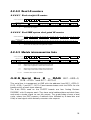
4.2.5 Serial
Bus
2
—
DAQ
(A21…A20)=0,
(A19…A18)=1 and (A17…A01)=0
This serial bus is transparent to VME with the address lines (A21…A20)=0,
(A19…A18)=1 and (A17…A01)=0 and communicates with the DACs for the
baseline shift of each input channel.
The 8-bit DACs used on the FADCTF boards are four Analog Devices
DAC8841 with 8 outputs each. They have serial address/data and clock lines
and need a strobe signal to set the output. The graph below shows a load
cycle, where the DAC expects 4 address bits followed by 8 data bits and
finally a load signal which actually executes the request.
18
Moreover, the DACs can be set to the central value (0x80) when a signal is
applied to the Preset input.
The address/data, clock and preset lines are common to all four DACs, only
the Load strobes are individual. Due to historical reasons, the first and last
DACs are only utilized by 50%.
The matching between analog inputs (1…24) and DACs (8 channels each) can
be found in the table below. The input numbering scheme follows the drawing
in the FADC User’s Manual (top to bottom).
Input
DAC
INP1-4
DAC 1
INP5-8
DAC 2
INP9-12
INP13-16
DAC 3
INP17-20
INP21-24
DAC 4
As mentioned above, only 4 out of 8 outputs are used on DAC 1 and DAC 4.
The VME address map is shown below:
VME bus addr/data bits
21 20
19 18 17 16
15 14 13 12
11 10
9
8
0
1
0
x
0
x
0
x
0
x
7
6
5
4
3
2
1
0
0
p
0
x
0
c
s
offset from F_BASE
DAC
Address
Data
0x0c0000
write
s
c
p
ld1
ld2
ld3
ld4
0
1
0
0
0
x
0
x
0
x
0
x
0 0 0 0
ld4 ld3 ld2 ld1
address/data line (SDI)
clock line (CLK)
preset all DAC outputs to 0x80
load strobe DAC1 (INP1-4)
load strobe DAC1 (INP5-12)
load strobe DAC1 (INP13-20)
load strobe DAC1 (INP21-24)
19
Sample Function: Set a specific DAC to a specified 8 bit value.
void LOAD_DAC8841(int inp, int ivalue)
// inp
= 1...24
(corresponding input channel)
// ivalue = 0...255 (8-bit DAC value)
{
int i;
/* Send serial address */
for (i=0;i<4;i++)
{
VXIout(3,F_BASE+DAC_Strobe,2,((((inp+3)&7)+1) & (8>>i)) ? 3 : 2);
}
/* Send serial data value */
for (i=0;i<8;i++)
{
VXIout(3, F_BASE+DAC_Strobe, 2, (ivalue & (128>>i)) ? 3 : 2);
}
/* Load DAC value */
VXIout (3, F_BASE+DAC_Strobe, 2, 0x10<<((inp+3)>>3));
}
20
5 Sequencer
5.1 Address Space
Very similar to the FADCTF modules, the Sequencer will have its own A32
address space representing a contiguous data block of 16MB (bits
A23…A0). The highest 8 address bits can be selected by two hex switches
on the PCB, which are located close to the rear end between the P1 and P2
connectors.
A32 address bits
31 30 29 28 27 26 25 24 23 22 21
SW2
2
1
SW1
The type of VME transfer should be set for non-privileged 32 bit data
access. Concerning the address modifier lines, only AM5=0 (32 bit data) is
required, we don’t care about AM0…AM4.
Let’s call the base address of the Sequencer S_BASE.
5.2 General functions
There is an “int”/”ext” switch on the Sequencer front panel. As long as it is
set to “ext” (right) position, the Sequencer will only repeat the TTM signals
regardless of the VME register settings. However, it is possible to select
the clock source to either TTM or the LEMO front panel input. The latter
expects TTL levels and has an adjustable threshold between 550 and
2950mV.
Alternatively, the internal quartz clock (and the standalone test functions)
can only be enabled if the switch is in “int” position.
5.2.1 Reset, TTM or standalone
VME bus addr bits
31 30 29 28
...
11 10
9
8
7
6
5
4
3
2
1
0
0
x
0
x
0
x
0
x
0
x
0
x
0
x
0
x
0
x
0
x
i
offset from S_BASE
Address
Data
0x00
write
sr
fr
x
x
0
x
sr=0
sr=1
-Sequencer reset
fr=0
fr=1
-FIFO reset (clear)
i=0
i=1
external mode: repeat/distribute TTM signals
internal mode: generate all signals by VME triggered sequencer
requires front-panel switch in "int" (left) position
21
5.2.2 Clock source
VME bus addr bits
31 30 29 28
...
11 10
9
8
7
6
5
4
3
2
1
0
offset from S_BASE
Address
Data
0x08
write
x
x
x
x
0
x
0
x
0
x
0
x
0
x
0
x
0
x
0
x
1
x
0
x
0
x
ttm
Address
Data
0x0c
write
x
x
x
x
0
x
0
x
0
x
0
x
0
x
0
x
0
x
0
x
1
x
1
x
0
x
q
Clock source selection in external mode (either set by switch or VME):
ttm=0
use TTM clock
ttm=1
use front panel clock input
Clock source selection in internal mode (set by switch and VME):
q=0
use front panel clock input
q=1
use internal quartz oscillator
The table below gives a summary which conditions must be met to select a
specific clock source. “—“ indicates that this mode is not possible. The clock
source is selected by one of ttm or q registers, where the other one is
irrelevant. Example: To select the quartz oscillator, internal mode must be
enabled both on the front panel switch and by VME, and q set to 1, while
ttm is “don’t care”.
Front panel
switch
Clock source (ADDR=0x08/0x0c)
VME mode
(ADDR=0x00)
TTM
Front panel
Quartz
don’t care
ttm=0
ttm=1
—
External, i=0
ttm=0
ttm=1
—
Internal, i=1
—
q=0
q=1
5.3 TTM L1.5 accept
The Sequencer can be used to generate a L1.5 accept (“Reject”) signal,
which is sent to the TTM with a custom cable. The pulse is then transmitted
over the TTM/Sequencer/P2 backplane.
VME bus addr bits
31 30 29 28
...
11 10
9
8
7
6
5
4
3
2
1
0
0
x
0
x
0
x
0
x
0
x
1
x
1
x
1
x
1
x
0
x
r
offset from S_BASE
Address
Data
0x3c
write
r=0
r=1
x
x
x
x
0
x
-generate L1.5 accept pulse on TTM_IO pins 27 and 28 (for test purposes)
22
5.4 Standalone test functions
Please note that the internal mode only becomes effective if the front panel
switch is set to “int” (left) position.
5.4.1 Normal readout cycle(s)
31 30 29 28
VME bus addr bits
...
11 10
9
8
7
6
5
4
3
0
x
0
x
0
x
0
x
0
x
0
x
0
x
0
x
2
1
0
offset from S_BASE
Address
Data
0x04
write
x
x
x
x
0
x
sta=0
sta=1
-generate readout sequence (including Fast-Or, EFT, start,...)
l15=0
l15=1
do not send L1.5 accept
send L1.5 accept after readout
sto=0
sto=1
loop readout sequence forever (until sto=1 is set)
stop after current readout sequence
1 0
sto l15 sta
NB: The sto signal can either be issued together with sta (generating a single sequence)
or at any later time (thus stopping after the current sequence has finished)
5.4.2 Simulate external test mode
VME bus addr bits
31 30 29 28
...
11 10
9
8
7
6
5
4
3
2
1
0
offset from S_BASE
N_START
N_RESET
Address
Data
0x10
write
x
x
x
x
0
x
0
x
0
x
0
x
0
x
0
x
0
x
1
x
0
x
0
x
0
x
x
Address
Data
0x14
write
x
x
x
x
0
x
0
x
0
x
0
x
0
x
0
x
0
x
1
x
0
x
1
x
0
x
x
Initially, the FADCTF boards should be switched to test mode.
A write operation to N_START generates a single ADCCLK5 window.
The width of this window is 200ns for the first 4 calls, then 4x400ns, 4x600ns,...
The number of stored samples depends on 5MHz (1,1,1,1,2,2,2,2,...) or
20MHz (4,4,4,4,8,8,8,8,...) readout speed.
A write operation to N_RESET resets the width of the clock window its initial state.
5.4.3 4-channel
(RJ45)
analog
test
output
NB: The front panel input signal is always added to the DAC output.
5.4.3.1 Automatic DAC ramp
VME bus addr bits
31 30 29 28
...
11 10
9
8
7
6
5
4
3
2
1
0
0
x
0
x
0
x
0
x
0
x
1
x
0
x
0
x
0
x
0
x
r
offset from S_BASE
Address
Data
0x20
write
r=0
r=1
x
x
x
x
0
x
disable automatic DAC ramp
enable automatic DAC ramp (200ns per step) during sequencer cycling
23
5.4.3.2 Set static DAC value
VME bus addr bits
31 30 29 28
...
11 10
9
8
7
6
5
4
3
2
1
0
0
x
0
x
0
x
0
x
0
d
0
d
1
d
1
d
1
d
0
d
d
offset from S_BASE
Address
Data
0x1c
write
d
x
x
x
x
0
x
(static) 7-bit DAC value (requires DAC ramp disabled)
5.5 PCI-Link test input
NB: The PCI-Link cable has to be connected to the dedicated Sequencer
input on the front panel.
The PCI-Link data format is explained in the FADC User’s Manual.
5.5.1 Read
XREQUEST,
trigger status
VME bus addr bits
31 30 29 28
...
BUSY
and
11 10
9
8
7
6
5
4
3
2
1
0
0
x
0
x
0
x
0
x
0
x
0
x
0
res
0
l1
1 0
l0 bus req
offset from S_BASE
Address
Data
0x04
read
req
bus
l0
l1
res
x
x
x
x
0
x
status of XREQUEST line
status of P2_TTM_BUSY (wired-or of all modules on the P2 backplane)
status of P2_L0 (wired-or of all modules on the P2 backplane)
status of P2_L1 (wired-or of all modules on the P2 backplane)
reserved
5.5.2 Set
PCI-Link
XREADY
VME bus addr bits
31 30 29 28
...
XENABLE
and
11 10
9
8
7
6
5
4
3
2
1
0
0
x
0
x
0
x
0
x
0
x
0
x
1
x
1
x
0
x
0
x
en
offset from S_BASE
Address
Data
0x18
write
en=0
en=1
x
x
x
x
0
x
set XENABLE and XREADY=high (idle condition)
set XENABLE and XREADY=low (ready to receive data)
5.5.3 Read PCI-Link data
VME bus addr bits
31 30 29 28
...
11 10
9
8
7
6
5
4
3
2
1
0
0
d
0
d
0
d
0
d
0
d
0
d
0
d
0
d
0
d
0
d
d
offset from S_BASE
Address
Data
0x00
read
d
d
d
d
d
0
d
32-bit PCI-Link FIFO (16k words) data
24