1
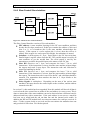
Digital module requirement specification
1-31
PHOS Board Controller Specification
Document name:
PHOS BC specification_v3.4.doc
Revision:
0.6 (fw version 3.4)
Date:
Created on 5/23/2007 9:38:00 AM
Last saved: 10/31/2007 11:12:00 AM
Author:
Created by Johan Alme
Last saved by Johan Alme
Module:
PHOS BC
Block diagram:
PHOS BC specification_v3.4.doc
Created by Johan Alme
Digital module requirement specification
2-31
Features:
•
•
•
•
•
•
•
•
•
•
•
•
•
•
•
Two command interfaces
o ALTRO bus interface
o Special I2C interface
I2C interface is robust with timeout counters and masking of bus input when
active transaction to other card.
Setting of DACs for bias voltage for High Voltage region
Interface to 3 ADCs for verifying voltage and current-levels as well as
temperatures.
Programmable min/and max thresholds for flagging errors in ADC values.
Possible to set how to treat the voltages read back for current calculations:
o Store them as is
o diff with previous adc value.
o Control the order of diff after the expected direction of the current
Unlock register for write to read-only registers
Monitoring error inputs from Power Regulators
Interrupt line to RCU for errors of a severity level craving urgent measures
Configurable number of threshold violations from 1 to 3 before interrupt is
flagged.
Possible to set the FEC in standby mode by turning off voltage regulators and
not reporting any warnings/errors.
Radiation precautions:
o Hamming coded ADC threshold settings
o Hamming coded DAC values
o TMR of configuration/status registers and threshold config registers
Configurable automatic update of DACs
Event-length Manager module that generates a hitmap of all ALTRO channels
and clocks this out to RCU by controlling dstb for Sparse Readout Mode.
Debug registers to test ALTRO bus integrity
PHOS BC specification_v3.4.doc
Created by Johan Alme
Digital module requirement specification
1
3-31
DOCUMENT CONTROL...................................................................................4
1.1
1.2
REVISION HISTORY ..........................................................................................4
REFERENCES ...................................................................................................4
2
MOTIVATION ....................................................................................................5
3
EXTERNAL INTERFACE.................................................................................6
3.1
3.2
SIGNAL INTERFACE .........................................................................................6
TIMING DIAGRAMS ..........................................................................................9
4
REGISTER INTERFACE ................................................................................10
5
FUNCTIONAL REQUIREMENTS.................................................................17
5.1
FUNCTIONAL OVERVIEW...............................................................................17
5.2
MAIN FUNCTIONAL CHANGES FROM PCM V2.0 (HUST) .............................17
5.3
PROJECT SETUP .............................................................................................17
5.3.1
Software ...............................................................................................19
5.4
FUNCTIONAL DETAILS ..................................................................................20
5.4.1
Main Output Signals ............................................................................20
5.4.2
Drivers (Glue Logic)............................................................................20
5.4.3
ALTRO Switch Mask In........................................................................20
5.4.4
ALTRO Interface..................................................................................20
5.4.5
Event-length Manager .........................................................................21
5.4.6
Slow Control Slave Interface ...............................................................22
5.4.7
Interface Decoder ................................................................................23
5.4.8
Registers...............................................................................................23
5.4.9
ADC Interface ......................................................................................24
5.4.10
DAC Interface ......................................................................................25
5.4.11
Hamming Code / Hamming Decoder Module .....................................26
5.4.12
Optional Functionality.........................................................................27
6
OTHER REQUIREMENTS .............................................................................28
6.1
CLOCK STRATEGY .........................................................................................28
6.2
RESET STRATEGY ..........................................................................................28
6.3
POWER STRATEGY.........................................................................................28
6.4
TEST STRATEGY ............................................................................................28
6.4.1
Functional and Post Place and Route Verification .............................28
6.4.2
Functional Coverage ...........................................................................29
6.4.3
Hardware Verification .........................................................................29
7
PHYSICAL IMPLEMENTATION..................................................................30
7.1
TECHNOLOGY ...............................................................................................30
7.2
LOGIC SYNTHESIS .........................................................................................30
7.2.1
Static timing analysis ...........................................................................30
7.2.2
Area estimates......................................................................................30
8
INSTALLATION LOG .....................................................................................31
8.1
8.2
INSTALLATION STATUS .................................................................................31
SOFTWARE ....................................................................................................31
PHOS BC specification_v3.4.doc
Created by Johan Alme
Digital module requirement specification
4-31
1 Document control
1.1 Revision history
Rev.
0.1
0.2
0.3
0.4
0.5
0.5
Rev. date
24.05.07
16.08.07
04.09.07
10.10.07
16.10.07
30.10.07
Document status
First draft
Updated after design of v3.0
Updated to match version 3.1 of firmware
Updated to match version 3.2 of firmware
Updated to match version 3.3 of firmware
Updated to match version 3.4 of firmware
Responsible
JA
JA
JA
JA
JA
JA
1.2 References
Ref. No.
1.
Doc. Name.
PCM_2_0.pdf
Rev / Rev date
Ver 2.0, Aug
2006
2.
AD7416_AD7417_7418.pdf
Rev. G [2004]
3.
4.
FEE-V1.1b.pdf
PHOS-User-Manual.pdf
5.
MAX5308-MAX5309.pdf
V1.1 27.Sep 05
Rev 2.1 4. Jan
07
Rev 0; 8/01
6.
TPC-BC_v2.3.pdf
9/12/2004
7.
acex.pdf
Ver 3.4, May
03
PHOS BC specification_v3.4.doc
Title
PCM 2.0 8Based on PHOSS
FEE board controller 0.1
(HUST)
Analog Devices 10-Bit Digital
Temperature Sensor (AD7416)
and Four Single-Channel ADCs
(AD7417/AD7418)
PHOS FEE v1.1 Schematics
PHOS Basics for the User
Maxim Low-Power, Low-Glitch,
Octal 10-Bit Voltage-Output
DACs with Serial Interface
ALICE TPC Board Controller
(version 2.3)
ALTERA Acex 1K
Programmable Logic Device
Family
Created by Johan Alme
Digital module requirement specification
5-31
2 Motivation
The Front End Electronics in PHOS is consisting of one Readout Control Unit
(RCU) and 28 Front End Cards (FECs) connected to the RCU via two separate
branches. On each FEC an SRAM based FPGA is situated – the Board Controller.
Since the Front End Electronics is physically unavailable when PHOS is fully
commissioned it must be possible to check the status via software during operation,
and quickly respond to any error situation that might occur.
The purpose of the Board Controller is to read crucial values on the FEC, such as
voltages, currents and temperatures. If these values exceed given programmable
thresholds the RCU will be notified. If the severity level is considered to be
potentially damaging to the board, the RCU will turn off the given FEC.
The PHOS FEC also includes a high voltage section. A very important
functionality of the PHOS Board Controller is to set the bias voltage to the charge
sensitive amplifiers located in the high voltage section. This must be done since the
amplification of the APDs that are used for readout is varying from part to part. This
variation is cancelled out with the setting of the DACs that are controlling the bias
voltage.
This version of the PHOS BC is based on the TPC BC, adding the extra
functionality needed for PHOS, and removing some features that are not needed. The
basis for the code is the FMD version that is a VHDL implementation of the TPC BC
with some modifications. Major changes have been done to this implementation to
make it fit for PHOS and to make it more robust.
PHOS BC specification_v3.4.doc
Created by Johan Alme
Digital module requirement specification
6-31
3 External Interface
3.1 Signal interface
Signal name
rdoclk
Dir
in
Pin
183
rdoclk_en
fecclk_40m
adcclk
adcclk_en
rst_fbc
out
in
in
out
out
121
79
167
122
101
sys_rst
bd[39:0]
in
Inout
write
Inout
80
[40,41,
44,45,
46,47,
53,54,
55,56,
57,58,
60,61,
63,64,
65,67,
68,69,
70,71,
73,74,
75,83,
85,86,
87,88,
89,90,
92,93,
94,95,
96,97,
99,100]
197
cstb
Inout
104
ackn
inout
205
error
inout
37
1
Sync1
Description
40 Mhz Readout Clock (used as system
clock)
Enable for the ALTRO readout clock
40 MHz Clock from crystal
20 MHz ALTRO sampling clock.
Enable signal for the ALTRO sampling clock
Reset from RCU (command decoded) –
active low
Global reset signal from power up
Bidirectional ALTRO bus:
[39] Parity bit
[38] Bcast bit
[37] Boardcontroller/ALTRO
[36:25] Channel Address / BC register
address
[24:20] ALTRO Instruction Code
[19:0] Data
The write/read signal is driven by the master
(RCU) and defines whether the access to the
addressed unit is in write/read mode
(low/high).
The master (RCU) drives the command
strobe (CSTB) signal. When asserted, it
indicates that a valid word has been placed in
the AD bus. The signal also qualifies the
WRITE signal.
On a WRITE or COMMAND cycle, the
addressed unit asserts the ACKN signal to
indicate that is has successfully latched the
bus content and executed the requested
instruction. On a READ cycle, the addressed
unit asserts the ACKN to indicate that it has
placed the requested data on the bus.
The ERROR line is asserted by the slave
units to signal the occurrence of an error
condition. If the error condition has occurred
in an instruction cycle (parity error or
Inputs:
<clock name>|async: Assumed synchronous with the given clock name or asynchronous
Ouputs: <clock_name>[glitch free]|comb: Output generated from the given clock name or combinatorial
PHOS BC specification_v3.4.doc
Created by Johan Alme
Digital module requirement specification
trsf
inout
39
dstb
inout
38
l1
In
102
l2
in
103
trsf_en
In
195
ack_en
In
193
dolo_en
In
186
card_ad[4:0]
in
bcout_add[4:0]
out
altrops_en
biasps_en
shaperps_en
allps_error
out
out
out
in
[176,
175,
174,
173,
172]
[192,
191,
190,
189,
187]
126
128
127
78
altrops_error
in
180
biasps_error
in
168
shaperps_error
in
163
oeab_l
out
202
oeab_h
out
160
PHOS BC specification_v3.4.doc
7-31
instruction code error), the slave does not
acknowledge the instruction cycle and asserts
the ERROR signal.
The ALTRO chip takes the control of the bus
by asserting the TRANSFER signal
acknowledges this instruction cycle.
TRANSFER is kept asserted till the data block
has been completely transferred.
The data transfer is not necessarily
continuous and for this reason each single
word, being transferred, is validated by the
signal DSTB (Data Strobe).
The l1 signal is broadcasted by the RCU to all
the FECs. It is used for the distribution of the
trigger information. The l1 signal is
synchronous with the SCLK signal and lasts
for at least two clock cycles.
The l2 signal is broadcasted by the RCU to all
the FECs. It is used for the distribution of the
trigger information. The l2 signal is
synchronous with the RCLK and lasts for two
clock cycles.
trsf_en is used to drive the bi-directional bus
bd when transferring an event.
ack_en frames ackn, enabling the intrinsic
capacitor in the transceiver.
dolo_en is used to drive the bi-directional bus
bd when reading a register for the later.
Hardware address input from branch
Output hardware address to the ALTROs:
“00000” if ALTROs are turned off or in debug
mode
card_ad otherwise.
Enable signal for ALTRO power regulators
Enable signal for bias power regulators
Enable signal for shaper power regulators
Error flag signalling if output voltage has
dropped 5% under nominal value for the
power regulator of the digital part.
Error flag signalling if output voltage has
dropped 5% under the nominal value for
ALTRO power regulator. Low parity
Error flag signalling if output voltage has
dropped 5% under the nominal value for bias
power regulator. Low parity
Error flag signalling if output voltage has
dropped 5% under the nominal value for
shaper power regulator. Low parity
Setting direction of GTL drivers for altro bus:
0: output (to RCU)
1: input (to FEC)
Setting direction of GTL drivers for altro bus:
0: output (to RCU)
1: input (to FEC)
Created by Johan Alme
Digital module requirement specification
oeba_l
out
200
oeba_h
out
196
ctr_in
out
198
ctr_out
out
199
rcu_scl
rcu_sda_in
rcu_sda_out
bc_int
sensor_scl
sensor_sda
convst
oti_1
oti_2
oti_3
dac_clk_en
dac_sclk
dac_ldac
in
in
out
out
out
inout
out
In
In
In
out
out
out
184
119
120
16
7
8
13
9
11
12
10
17
203
dac_sel[3:0]
out
[26, 25,
24, 18]
dac_din[3:0]
out
dac_dout[3:0]
in
test_m_sclk_dn
out
[30, 29,
28, 27]
[36, 31,
15, 14]
166
test_m_sclk_dn
out
164
test_m/g
in
157
tms_altro0
tms_altro1
tms_altro2
tms_altro3
adc_add[1:0]
out
out
out
out
out
111
112
113
114
[116,
115]
led_red
out
62
PHOS BC specification_v3.4.doc
8-31
Setting direction of GTL drivers for altro bus:
1: output (to RCU)
0: input (to FEC)
Setting direction of GTL drivers for altro bus:
1: output (to RCU)
0: input (to FEC)
Enabling output of GTL drivers for control bus
(RCU->FEC):
0: enabled
1: high Z
Enabling output of GTL drivers for control bus
(FEC -> RCU):
0: enabled
1: high Z
5 MHz Slow Clock for I2C transfers
Slow Control Serial data in from RCU
Slow Control Serial data out to RCU
Interrupt line to RCU, Active Low.
I2C clock for AD7417 communication (x3)
I2C data line for AD7417 communication (x3)
Convert start signal for AD7417 (x3)
Over-temperature indicator (Not used)
Over-temperature indicator (Not used)
Over-temperature indicator (Not Used)
DAQ serial clock enable. Active high
DAC serial Clock
Load DAC. LDAC is asynchronous active-low
that updates the DAC outputs simultaneously.
If LDAC is driven low, the DAC registers are
transparent.
Chip-Select output (active-low)
daq_sel[0] – HVB 1 – 8
daq_sel[1] – HVA 1 – 8
daq_sel[2] – HVA 9 – 16
daq_sel[3] – HVB 9 – 16
Serial Data Input for the 4 dacs
Data Output from the 4 daqs. DOUT is
updated on the falling edge of SCLK.
LVDS_n Test mode sampling clock generated
by the Board Controller. Can only be used of
external SCLK is missing
LVDS_p Test mode sampling clock generated
by the Board Controller
Enable signal to enable test sampling clock
and RCLK for BC. Active low.
Test mode Altro 0, active low (Not Used)
Test mode Altro 4, active low (Not Used)
Test mode Altro 2, active low (Not Used)
Test mode Altro 3, active low (Not Used)
Output addressing lines for testmode. Used to
address which of the 4*4 channels in the
ALTROS should be readout during testmode
execution.
“00” – ch 0-3, “01” – ch 4-7,
“10” – ch 8-11, “11” – ch 12-15
Not Used
Output to diode (connected high)
Created by Johan Alme
Digital module requirement specification
led_yellow
led_green
aux[3:0]
out
out
out
usb_sda
usb_scl
usb_ef
usb_rw
usb_cs
usb_fd[15:0]
inout
in
out
in
in
inout
usb_clr_fifo
usb_ifclk
usb_ff
out
in
out
179
177
[162,
161,
159,
158]
208
207
206
170
169
[150,
149,
148,
147,
144,
143,
142,
141,
140,
139,
136,
135,
134,
133,
132,
131]
125
182
204
9-31
Output to diode (connected high)
Output to diode (connected high)
Output to diode (connected high)
USB interface - Not Used
USB interface - Not Used
USB interface - Not Used
USB interface - Not Used
USB interface - Not Used
USB interface - Not Used
USB interface - Not Used
USB interface - Not Used
USB interface - Not Used
Table 3-1: Signal interface
3.2 Timing diagrams
TBA
PHOS BC specification_v3.4.doc
Created by Johan Alme
Digital module requirement specification
10-31
4 Register interface
Register name
Addr.
Type
UNLOCK
0x0
RW
Allow
Brcast
Yes
L0CNT[15:0]
L2CNT[15:0]
SCLKCNT[15:0]
SLOWCTR_ERR
[7:0]
CSR0[11:0]
0x0B
0x0C
0x0D
0x0E
R(W)
R(W)
R(W)
R
Yes*
Yes*
Yes*
No
0x11
RW
Yes
CSR1[13:0]
0x12
R
N/A
2
2
Description
One bit unlock register for writing to read
only regs for testing.
0: Locked
1: Unlocked
Number of L0 triggers received
Number of L2a triggers received
Sampling clock counter
Number of timeout situations in Slow
Control
Interrupt Mask Register:
Default value = 0x1FF
[11]
HV Update Mode.
0 = The BC updates DAC with
update_hv command.
1 = The BC continuously updates
DACs
[10]
Conversion Mode.
0 = The BC reads the content of
the monitor ADC with the STCNV
command (1B)
1 = monitor ADC converts
continuously
[9:8]
Error Mask. These two bits
mask the assertion of the Error
line. This line is asserted with the
flags registered in CSR1[9:8]
0 = the error is masked
1 = the error asserts the line
[7:0]
Interrupt Mask. These bits mask
the bits of CSR1 [7:0] for the
assertion of the Interrupt line
Error Status Register:
Default value = 0x0000
[13]
Value of Slow Control Interrupt
line
[12]
Value of ALTRO bus Error line
[11]
Slow Control Instruction Error
[10]
ALTRO error: Registered value
of ALTRO bus error line
[9]
ALTRO bus Instruction Error (to
BC)
[8]
Parity error of ALTRO bus 20
MSB
[7]
Missing Sampling Clock
[6]
ALTRO Power, Digital 4.2V &
3.3V and Bias Supply Error
[5]
Shaper +6.0V Power Supply
Error
[4]
4.2 V or 3.3 V digital current is
higher than thresholds.
[3]
4.2 V or 3.3 V digital voltage is
lower than thresholds.
Legend: W=write, R=read, T= write trigger (not physical registers)
PHOS BC specification_v3.4.doc
Created by Johan Alme
Digital module requirement specification
Register name
Addr.
Type
2
11-31
Allow
Brcast
Description
[2]
CSR2[15:0]
0x13
RW
Yes
CSR3[15:0]
0x14
RW
Yes
DEBUG[1:0]
0x15
R
No
CNTLAT
CNTCLR
CSR1CLR
ALRST
BCRST
STCNV
SCEVL
0x16
0x17
0x18
0x19
0x1A
0x1B
0x1C
T
T
T
T
T
T
T
Yes
Yes
Yes
Yes
Yes
Yes
Yes
EVLRDO
0x1D
T
Yes
UPDATEHV
BCVERSION[15:0]
0x1E
0x20
T
R
Yes
N/A
PHOS BC specification_v3.4.doc
4.0 V, +6.0 V, -6.0 V, 13.5 V
analog current higher than
threshold.
[1]
4.0 V, +6.0 V, -6.0 V, 13.5 V
analog voltage lower than
threshold.
[0]
Temp1, Temp2 or Temp3 higher
than threshold.
Status and Configuration
Default value = 0x013F
[15:11] Hardware Address (read only)
[10]
Card Isolated
[9:8]
Number of times a ADC
threshold violation must occur
before it is reported
[7]
Not Used
[6]
Enables Hamming correction on
HVDAC values and Thresholds.
[5]
Enables DAC clock
[4]
Enables Sampling Clock
[3]
Enables Readout Clock
[2]
Power Switch for Shaper Power
Regulator
[1]
Power switch for Bias Power
Regulator
[0]
Power switch for ALTRO Power
Regulator
Status and Configuration
Default value = 0x2220
[15]
This bit is set to 1 when the BC
has completed the transaction
with the mADC. It is reset at the
beginning of every transaction.
[14:8] Scevl timeout value. Max num of
clks for each transaction on the
ALTRO bus when BC is master.
[7:0]
rdclk / sclk warning ratio
[1]
Value of Slow Control data line
[0]
Value of test_mg input
Latch L0, L2, SCLK counters
Clear L0, L2, SCLK counters
Clear Error Status Register
Reset all the ALTROs
Reset Board Controller to default values
Start Conversion / Readout monitor ADC
Scan Event-length registers in all ALTRO
channels
Start readout of Event Length Hitmap
register.
Update HV
Board Controller Version
Created by Johan Alme
Digital module requirement specification
12-31
Register name
Addr.
Type
VTS_HIGH[14:0]
0x21
R(W)
Allow
Brcast
Yes*
VTS_LOW[14:0]
0x22
R(W)
Yes*
TH_HMGERR_HIG
H[14:0]
TH_HMGERR_LOW
[14:0]
HV_FB1[15:0]
0x23
R(W)
Yes*
0x24
R(W)
Yes*
0x25
R(W)
Yes*
HV_FB2[15:0]
0x26
R(W)
Yes*
HV_HVHMGERR1
[15:0]
0x27
R(W)
Yes*
HV_HVHMGERR2
[15:0]
0x28
R(W)
Yes*
ADC_DIFF[14:0]
0x29
RW
Yes
PHOS BC specification_v3.4.doc
2
Description
Voltage Temperature Status register:
[0] TEMP1 over th
[1] D4V0 over th
[2] D4V0C over th
[3] D3V3 over th
[4] D3V3C over th
[5] TEMP2 over th
[6] A6nV0 over th
[7] A6nV0C over th
[8] A6pV0 over th
[9] A6pV0C over th
[10] TEMP3 over th
[11] A3V3 over th
[12] A3V3C over th
[13] A13V0 over th
[14] A13V0C over th
Voltage Temperature Status register:
[0] TEMP1 under th
[1] D4V0 under th
[2] D4V0C under th
[3] D3V3 under th
[4] D3V3C under th
[5] TEMP2 under th
[6] A6nV0 under th
[7] A6nV0C under th
[8] A6pV0 under th
[9] A6pV0C under th
[10] TEMP3 under th
[11] A3V3 under th
[12] A3V3C under th
[13] A13V0 under th
[14] A13V0C under th
Double hamming errors found in ADC
high threshold memory .
Double hamming errors found in ADC low
threshold memory.
Compared outputs from DAC for CSP
[7:0]
CSP 16 – CSP 23
[15:8] CSP 7 – CSP 0
0: DAC not set/Wrong
1: DAC set/Correct
Compared outputs from DAC for CSP
[7:0]
CSP 15 – CSP 8
[15:8] CSP 24 – CSP 31
0: DAC not set/Wrong
1: DAC set/Correct
Double hamming errors for the following:
[7:0]
CSP 16 – CSP 23
[15:8] CSP 7 – CSP 0
Double hamming errors for the following:
[7:0]
CSP 15 – CSP 8
[15:8] CSP 24 – CSP 31
Sets which ADC values that should be
treated as currents in the ADC value and
ADC threshold memory. In practice this is
a diff between Vprev and Vcurrent
Default Value: 0x5294
Created by Johan Alme
Digital module requirement specification
Register name
Addr.
Type
ADC_DIFF_DIR
[14:0]
0x2A
R(W)
2
13-31
Allow
Brcast
Yes*
Description
Sets the expected direction of the current
for the current measurements given by
ADC_DIFF register.
0: Current = Vpreviou - Vcurrent
1: Current = Vcurrent – Vpreviou
Default Value: 0x0080
TRANS_CNT[15:0]
0x2B
R
No
LAST_ADDR_MSB
[7:0]
0x2C
R
No
LAST_VALID_ADDR
[15:0]
LAST_NOTVALID_
ADDR[15:0]
0x2D
R
No
0x2E
R
No
ADC Min Threshold
Memory[14:0]
0x30 –
0x3E
RW
Yes
ADC Max Threshold
Memory[14:0]
0x40 –
0x4E
RW
Yes
ADC Data
Memory[9:0]
HV DAC settings
memory
[14:0]
0x50 –
0x5E
0x60 –
0x7F
RW
Yes
RW
Yes
[15:8]
[7:0]
Number of acks sent to RCU
Number of strobes received from
RCU
[7:4]
MSB of last valid address
received.
[3:0]
MSB of last not valid address
received
LSB of last valid address received at the
FEC
LSB of the last not valid address received
at the FEC.
Min Threshold for the ADCs
[15:11] Hamming code
[10]
0: Threshold for Voltage
1: Threshold for Current
[9:0]
Data value
Max Threshold for the ADCs
[15:11] Hamming code
[10]
0: Threshold for Voltage
1: Threshold for Current
[9:0]
Data value
Data values from the ADCs
[9:0]
Data value
High voltage bias value for CSPs
0x60-0x67: CSP 23 down to CSP 16
0x68-0x6F: CSP 0 to CSP 7
0x70-0x77: CSP 8 to CSP 15
0x78-0x7F: CSP 31 down to CSP 24
[15:11] Hamming code
[10]
Don’t care (not used)
[9:0]
Value to Write
Table 4-1: List of registers that can be accessed externally. Note: The registers marked with
“R(W)” and Broadcast “Yes*” can be written to when unlock bit is set.
PHOS BC specification_v3.4.doc
Created by Johan Alme
Digital module requirement specification
Memory location name
TEMP1-MIN_TH
Addr.
0x30
D4V0_MIN_TH[
0x31
D4V0C_MIN_TH
0x32
D3V3_MIN_TH
0x33
D3V3C_MIN_TH
0x34
TEMP2-MIN_TH
0x35
A6nV0_MIN_TH
0x36
A6nV0C_MIN_TH
0x37
A6pV0_MIN_TH
0x38
A6pV0C_MIN_TH
0x39
TEMP3-MIN_TH
0x3A
A3V3_MIN_TH
0x3B
A3V3C_MIN_TH
0x3C
A13V0_MIN_TH
0x3D
A13V0C_MIN_TH
0x3E
14-31
Description
Minimum Temperature Threshold for ADC IC13
Default Data Value: 0x0 (disabled)
Minimum 4.0V Digital Voltage Threshold
Default Data Value: 0x1D8 (= 3.8 V)
Minimum 4.0V Digital Current Threshold
Default Value: 0x0 (disabled)
Alternatively Voltage level used for current calc.
Minimum 3.3V Digital Voltage Threshold
Default Data Value: 0x1C2 (= 2.9 V)
Minimum 3.3V Digital Current Threshold
Default Value: 0x0 (disabled)
Alternatively Voltage level used for current calc.
Minimum Temperature Threshold for ADC IC15
Default Value: 0x0 (disabled)
Minimum -6.0V Analog Voltage Threshold
Default Data Value: 0x170 (= -6.4 V)
Minimum -6.0V Analog Current Threshold
Default Value: 0x0 (disabled)
Alternatively Voltage level used for current calc.
Minimum 6.0V Analog Voltage Threshold
Default Data Value: 0x1E8 (= 5.6 V)
Minimum 6.0V Analog Current Threshold
Default Value: 0x0 (disabled)
Alternatively Voltage level used for current calc.
Minimum Temperature Threshold for ADC IC14
Default Value: 0x0 (disabled)
Minimum. 3.3V Analog Voltage Threshold
Default Value: 0x1C2 (= 2.9 V)
Minimum 3.3V Analog Current Threshold
Default Value: 0x0 (disabled)
Alternatively Voltage level used for current calc
Minimum 13.0V Analog Voltage Threshold
Default Value: 0x1D6 (= 12.6 V)
Minimum 13.0V Analog Current Threshold
Default Value: 0x0 (disabled)
Alternatively Voltage level used for current calc
Table 4-2: ADC Minimum Threshold Value Memory. The conversion factors are given in Table
4-4
PHOS BC specification_v3.4.doc
Created by Johan Alme
Digital module requirement specification
Memory location name
TEMP1-MAX_TH
Addr.
0x40
D4V0_MAX_TH[
0x41
D4V0C_MAX_TH
0x42
D3V3_MAX_TH
0x43
D3V3C_MAX_TH
0x44
TEMP2-MAX_TH
0x45
A6nV0_MAX_TH
0x46
A6nV0C_MAX_TH
0x47
A6pV0_MAX_TH
0x48
A6pV0C_MAX_TH
0x49
TEMP3-MAX_TH
0x4A
A3V3_MAX_TH
0x4B
A3V3C_MAX_TH
0x4C
A13V0_MAX_TH
0x4D
A13V0C_MAX_TH
0x4E
15-31
Description
Maximum Temperature Threshold for ADC IC13
Default Data Value: 0xA0 (= 40°C)
Maximum 4.0V Digital Voltage Threshold
Default Value: 0x0 (disabled)
Maximum 4.0V Digital Current Threshold
Default Value: 0x00C (=0.36 A)
Alternatively Voltage level used for current calc.
Maximum 3.3V Digital Voltage Threshold
Default Value: 0x0 (disabled)
Maximum 3.3V Digital Current Threshold
Default Value: 0x011 (= 0.73 A)
Alternatively Voltage level used for current calc.
Maximum Temperature Threshold for ADC IC15
Default Data Value: 0xA0 (= 40°C)
Maximum -6.0V Analog Voltage Threshold
Default Value: 0x0 (disabled)
Maximum -6.0V Analog Current Threshold
Default Value: 0x00F (=0.44 A)
Alternatively Voltage level used for current calc.
Maximum 6.0V Analog Voltage Threshold
Default Value: 0x0 (disabled)
Maximum 6.0V Analog Current Threshold
Default Value: 0x016 (= 0.764 A)
Alternatively Voltage level used for current calc.
Maximum Temperature Threshold for ADC IC14
Default Data Value: 0xA0 (= 40°C)
Maximum. 3.3V Analog Voltage Threshold
Default Value: 0x0 (disabled)
Maximum 3.3V Analog Current Threshold
Default value: 0x014 (= 0.858 A)
Alternatively Voltage level used for current calc
Maximum 13.0V Analog Voltage Threshold
Default Value: 0x0 (disabled)
Maximum 13.0V Analog Current Threshold
Default Value: 0x00F (= 0.334 A)
Alternatively Voltage level used for current calc
Table 4-3: ADC Maximum Threshold Value Memory
PHOS BC specification_v3.4.doc
Created by Johan Alme
Digital module requirement specification
16-31
Memory
location
name
TEMP1
Addr.
Description
Conv. factor
0x50
Temperature for ADC IC13
D4V0
0x51
4.0V Digital Voltage
D4V0C
0x52
D3V3
0x53
4.0V Digital Current
Alternatively Voltage level used for current calc.
3.3V Digital Voltage
D3V3C
0x54
TEMP2
0x55
3.3V Digital Current
Alternatively Voltage level used for current calc.
Temperature for ADC IC15
A6nV0
0x56
-6.0V Analog Voltage
A6nV0C
0x57
A6pV0
0x58
A6pV0C
0x59
TEMP3
0x5A
-6.0V Analog Current
Alternatively Voltage level used for current calc.
6.0V Analog Voltage
Default Data Value: 0x1E8 (= 5.6 V)
6.0V Analog Current
Alternatively Voltage level used for current calc.
Temperature for ADC IC14
A3V3
0x5B
3.3V Analog Voltage
A3V3C
0x5C
A13V0
0x5D
3.3V Analog Current
Alternatively Voltage level used for current calc
13.0V Analog Voltage
A13V0C
0x5E
0.25°C * ADC
counts
8.04mV * ADC
counts
29.8mA * ADC
counts
6.44 mV * ADC
counts
42.9 mA * ADC
counts
0.25°C * ADC
counts
4.88mV * ADC
counts / 1000 8.2V
29.3mA * ADC
counts
11.4 mV * ADC
counts
34.73 mA * ADC
counts
0.25°C * ADC
counts
6.44 mV * ADC
counts
42.9 mA * ADC
counts
26.8 mV * ADC
counts
22.3 mA * ADC
counts
13.0V Analog Current
Alternatively Voltage level used for current calc
Table 4-4: ADC Value Memory. Please note that the current conversion factors are only correct
if current mode is set in the Threshold register for given ADC value
PHOS BC specification_v3.4.doc
Created by Johan Alme
Digital module requirement specification
17-31
5 Functional Requirements
5.1 Functional Overview
The main features of the PHOS Board Controller are:
• Control the ALTRO bus and the GTL drivers on the FEC.
• Read temperatures, voltages and currents on the board and verify them against
locally stored thresholds. Flag if an error situation has occurred on the board.
• Set the output of the DACs that control the bias of the high voltage section.
• Read Eventlength registers in ALTRO and push hitmap data to the RCU when
Sparse Readout Mode is selected.
In addition the Board Controller is able to set the FEC in standby mode by
turning off the power supplies and disabling the clock and bus transactions.
Hamming is per default enabled, while continuously checking ADC values are
not. Before turning on continuously check on ADC values all threshold should be set
correctly. This includes adc_diff and adc_diff_dir registers – which in practice
decides whether one should read current or voltage from the ADC. These memory
location are set correctly by default. The Hamming encoding spans also over bit 10:0
in the threshold and dac registers.
The hamming decoding and, if needed, correction is done every time the
values from the memories are read by internal logic. When reading the ADC values
they are checked against the thresholds given in the min max threshold memories if
the threshold memory location value is unequal to 0. If 0, this means that the test is
disabled. The VTS registers (and CSR1) are set after the configurable number (1-3) of
times a threshold is violated for each value. The number of times is set by CSR2 bit
8:7, and is default set to 1. If a given threshold is unequal to 0, this means that a
violation of this threshold will trigger the interrupt line to the RCU.
5.2 Main Functional Changes From PCM v2.0 (HUST)
•
•
•
•
•
•
Removal of USB communication
Removal of Board ID register
Hamming encoding and TMR of static registers.
Some register remapping.
Thresholds and ADC values stored in memories
Removed Testmode
5.3 Project Setup
The complete design is checked into the CVS Repository of the Experimental Nuclear
Physics group, University of Bergen3, under the folder /vhdlcvs/phos_bc/.
File
bc.cr.mti
bc.mpf
func.do
ppr.do
Folder
/
/
/
/
fmd.rar
/code-ref/
3
Description
Questasim project file.
Questasim configuration file
Executes functional simulation
Executes post place and route
simulation.
Fmd project
http://web.ift.uib.no/kjekscgi-bin/viewcvs.cgi/
PHOS BC specification_v3.4.doc
Created by Johan Alme
Digital module requirement specification
File
PCM2.0_061130_2.rar
PCM2.0_061130_code.rar
PHOS BC specification.doc
PHOS_BC_specification_v3.1.doc
Folder
/code-ref/
/code-ref/
/docs/
/docs/
conv factor.xls
Graphics.vsd
*
/docs/
/docs/graphics
/docs/ref/
*
/Quartus_project/
bc.vhd
bc_tb2.vhd
register_config.vhd
altro_sw_mask_in.vhd
/vhdl/
/vhdl/
/vhdl/
/vhdl/
altro_sw_mask_in
vhdl\
altrobusinterface
vhdl\
altrobusinterface
vhdl\
altrobusinterface
vhdl\
altrobusinterface
/vhdl/drivers
/vhdl/drivers
/vhdl/drivers
/vhdl/evl_man/
/vhdl/evl_man/
/vhdl/evl_man/
/vhdl/evl_man/
/vhdl/hvdac
/vhdl/hvdac
/vhdl/interface_adc
/vhdl/interface_adc
/vhdl/interface_adc
/vhdl/interface_adc/
/vhdl/interface_adc
/vhdl/interface_adc
/vhdl/interface_adc
/vhdl/interface_adc
/vhdl/interface_adc
/vhdl/interface_adc
/vhdl/interface_adc
/vhdl/interfacedec
/vhdl/registers
/vhdl/registers
/vhdl/registers
/vhdl/registers
/vhdl/registers
/vhdl/registers
/vhdl/registers
/vhdl/registers
/vhdl/registers
/vhdl/registers
alprotocol_if.vhd
altrobusinterface.vhd
altrobusinterface_tb.vhd
interfacebus.vhd
drivers.vhd
signals_driver.vhd
transceivers_driver.vhd
ch_counter.vhd
evl_man.vhd
evlreg_trsf.vhd
read_evl.vhd
hvdac.vhd
hvdac_tb.vhd
adc_rom.cmp
adc_rom.vhd
interface_adc.vhd
interface_adc_tb.vhd
master.vhd
master_sm.vhd
ROM.hex
ROM.mif
rom.vhd
sequencer.vhd
serializer.vhd
interfacedec.vhd
adc_ram.cmp
adc_ram.vhd
counters.vhd
dac_ram.cmp
dac_ram.vhd
df_adcval.hex
df_adcval.mif
df_dac.hex
df_dac.mif
df_thhigh.hex
PHOS BC specification_v3.4.doc
18-31
Description
HUST PCM2.0 project
HUST PCM2.0 verilog
PHOS BC v3.0 spec
PHOS BC v3.1 spec (this
document)
Hamming encoding basis
Visio file with graphics
Documents that are used as
reference for the design
The files generated/used by
Quartus. Important files are:
• bc.pof,
bc.sof:
configuration files
• bc.vho: Simulation model
• bc.pin: Pinning file
Top level
Testbench
Package
See chapter 5.4.3
See chapter 5.4.4 (obsolete v3.3)
See chapter 5.4.4
See chapter 5.4.4 (not updated)
See chapter 5.4.4 (obsolete v3.3)
See chapter 5.4.2
See chapter 5.4.2
See chapter 5.4.2
See chapter 5.4.5
See chapter 5.4.5
See chapter 5.4.5
See chapter 5.4.5
See chapter 5.4.10
See chapter 5.4.10
See chapter 5.4.9
See chapter 5.4.9
See chapter 5.4.9
See chapter 5.4.9 (not updated)
See chapter 5.4.9
See chapter 5.4.9
See chapter 5.4.9
See chapter 5.4.9
Obsolete
See chapter 5.4.9
See chapter 5.4.9
See chapter 5.4.7
See chapter 5.4.8
See chapter 5.4.8
obsolete
See chapter 5.4.8
See chapter 5.4.8
See chapter 5.4.8
See chapter 5.4.8
See chapter 5.4.8
See chapter 5.4.8
See chapter 5.4.8
Created by Johan Alme
Digital module requirement specification
File
df_thhigh.mif
df_thlow.hex
df_thlow.mif
dstb_counter.vhd
hamming_decoder.vhd
registers.vhd
registers_block.vhd
sclk_counter.vhd
th_ram.hex
th_ram.mif
triggercounter.vhd
vtc_status.vhd
fec_address.vhd
sel_signals.vhd
serializer_bc.vhd
slave.vhd
slave_rx.vhd
slave_tb.vhd
slave_tx.vhd
ad7417.vhd
ad7417_tb.vhd
max5308dac.vhd
rcu_synthesis.vhd
tb_pkg.vhd
tb_pkg_phosBC.vhd
tb_txt_util.vhd
19-31
Folder
/vhdl/registers
/vhdl/registers
/vhdl/registers
/vhdl/registers
/vhdl/registers
/vhdl/registers
/vhdl/registers
/vhdl/registers
/vhdl/registers
/vhdl/registers
/vhdl/registers
/vhdl/registers
/vhdl/slave
/vhdl/slave
/vhdl/slave
/vhdl/slave
/vhdl/slave
/vhdl/slave
/vhdl/slave
/vhdl/testbench
/vhdl/testbench
/vhdl/testbench
/vhdl/testbench
/vhdl/testbench
/vhdl/testbench
/vhdl/testbench
Description
See chapter 5.4.8
See chapter 5.4.8
See chapter 5.4.8
obsolete
See chapter 5.4.8
See chapter 5.4.8
See chapter 5.4.8
See chapter 5.4.8
obsolete
obsolete
See chapter 5.4.8
See chapter 5.4.8
See chapter 5.4.6
See chapter 5.4.6
See chapter 5.4.6
See chapter 5.4.6
See chapter 5.4.6
See chapter 5.4.6 (not updated)
See chapter 5.4.6
See chapter 6.4
See chapter 6.4 (not updated)
See chapter 6.4
See chapter 6.4
See chapter 6.4
See chapter 6.4
See chapter 6.4
Table 5-1: Files checked in in the CVS repository.
5.3.1 Software
Editor:
Simulation:
Synthesis and Place and Route for test:
PHOS BC specification_v3.4.doc
ConTEXT v0.98.5
Questasim 6.1d
Quartus II Version 6.0 Build 178
Created by Johan Alme
Digital module requirement specification
20-31
5.4 Functional Details
5.4.1 Main Output Signals
Signal Name
rdoclk_en
adcclk_en
Ackn
Error
trsf
dstb
bcout_add[4:0]
altrops_en
biasps_en
shaperps_en
oeab_l
oeab_h
oeba_l
oeba_h
ctr_in
ctr_out
rcu_sda_out
bc_int
sensor_scl
sensor_sda
convst
dac_clk_en
dac_sclk
dac_ldac
dac_sel[3:0]
dac_din[3:0]
Explanation
Enables the distribution of the system clock to all the ALTROs.
Enables distribution of the sampling clock to the ADCs.
ALTRO bus acknowledge line
ALTRO bus error line
ALTRO bus transfer line
ALTRO bus data strobe
Masked address to ALTRO
ALTRO power supply enable
BIAS power supply enable
SHAPER power supply enable
ALTRO bus GTL driver enable
ALTRO bus GTL driver enable
ALTRO bus GTL driver enable
ALTRO bus GTL driver enable
CONTROL bus GTL driver enable
CONTROL bus GTL driver enable
Slow control data out
Interrupt line
ADC I2C interface
ADC I2C interface
ADC interface convert start
DAC serial interface
DAC serial interface
DAC serial interface
DAC serial interface
DAC serial interface
Table 5-2: Main output signals with explanations
5.4.2 Drivers (Glue Logic)
The purpose of the Drivers Module is twofold. Firstly it is in charge of driving
the direction of the GTL bus drivers for the ALTRO bus and the CONTROL bus, and
secondly it tristates the signals on the bus since the Front End Bus is common for all
FECs connected to the RCU.
5.4.3 ALTRO Switch Mask In
The ALTRO Switch Mask In Module is a combinatorial masking of ALTRO
bus input signals and internal mask bits. The internal mask bits are the power supplies
enable bits from CSR3. If the ALTRO power supplies are turned off, all
communication with the ALTROs are masked out, as well as error/status information
concerning the ALTRO to the RCU. If the BIAS and the SHAPER power supplies are
turned off, error/status information concerning the ALTRO to the RCU are masked
out.
Additionally it adds metastability filter on the strobe and acknowledge signal.
5.4.4 ALTRO Interface
As given by the name the ALTRO interface decoded the information coming
on the ALTRO bus. It listens for a positive edge on the strobe and then looks at the 20
PHOS BC specification_v3.4.doc
Created by Johan Alme
Digital module requirement specification
21-31
most significant bits in the ALTRO bus where it decodes the address. Decoding the
address essentially means:
• Decoding parity bit to detect any parity error Æ Not valid transaction
• Check the bcast bit. If asserted, no ack should be given
• Check the ALTRO_BC bit that selects either ALTRO or BC.
• Check the hardware address.
If all these are correct for the given FEC and Board Controller, the 7 least significant
bits are handed over to the registers module for decoding and the transaction is ack.
The transaction will be acked no matter if the given register addresses does exist or
not.
Two chip select signals are being decoded, one for if it is a valid board
controller transaction and one if it is a valid ALTRO transaction. These CS are used
by the Drivers Module to control the GTL bus drivers.
Since the ALTRO bus has a problem with occasional timeouts, debug
information was from version 3.4 made available in 4 registers. This information
gives a notice on how many strobes the BC has seen from the FEC and how many has
actually been acked. In addition the last 20 bit address being acked on the ALTRO
bus is stored, as well as the last 20 bit address that has not being acked is stored. This
can be used for debugging why the given BC does not ack on registers where it
should’ve done so.
Version 3.4 also introduced more robustness measures concerning the bus
such as meta-stability filters on all control signals and address information and an
extra wait state to be sure that the data/address are stable when the are decoded.
5.4.5 Event-length Manager
The Event-length Manager is used in Sparse Readout Mode, and the purpose
of the Event-length Manager is to scan the Event Length register of each ALTRO
channel to see if it contains data (zero-suppression must be enabled). The module
builds a hitmap register that has one bit for each channel that has event length unlike
zero. The hitmap register is pushed to the RCU in the same manner as the ALTRO
pushes data.
The Event-length manager listens on two commands from the register block
(decoded from the RCU)
• Scan Eventlength (SCEVL)
• Event-length Readout (EVL_RDO)
The first command starts to read the event length register of all the ALTRO
channels. To do this it needs to take control over the ALTRO bus and become the bus
master. It then isolates the board from the RCU for a short while wile doing this.
When the hitmap register is filled, it waits for the event-length readout command on
which it pushes the data to the RCU.
Please note: The pushing of the data uses a gated version of the rdoclk as dstb
as this is done originally. This is not an ideal solution and might lead to glitches and
misbehaviour of Sparse Readout Mode. It would be better to let the dstb run on half
the speed making a registered output as the dstb.
PHOS BC specification_v3.4.doc
Created by Johan Alme
Digital module requirement specification
22-31
5.4.6 Slow Control Slave Interface
Figure 5-1: Sketch of Slow Control Interface.
The Slow Control Interface consists of five sub-modules:
• FEC address: A state machine listening for the I2C start condition, and then
decode the first byte transferred. If this byte contains the address of this card
(bits 5 to 1), or is broadcast (bit 6), the state machine acknowledges the
request. If the request is a write request (bit 0 is low), then the receiver is
started. If the request is a read request (bit 0 high), the transmitter is started.
• Serializer: A shift-register of 1 byte. Serial input is the I2C bus serial data.
Parallel input is register values from the BC. The parallel output is used by all
state machines to get the needed data. The serial output is used by the
transmitter to serialize the parallel input to the master of the I2C bus.
• Slave RX: Receives one 1 byte, and compares the lower 7 bit to valid
instructions. If the instruction is correct, then the state machine acknowledges
the request and reads 2 more bytes. The instruction code and 16bit data is
output for handling by the BC.
• Slave TX: Receives one 1 byte, and compares the lower 7 bit to valid
instructions. If the instruction is correct, then the state machine acknowledges
the request. The instruction code is sent off to the BC, and valid data should be
returned. The transmitter then transfers the data in 2 1-byte blocks to the
master of the I2C bus.
• Select Signals: A multiplexer. Depending on the state of the various state
machines, this mux chooses the control inputs to the serializer, and the address
returned to the BC.
In version 3.2, this module has been upgraded. Now this module will decode all that is
received on the slow control bus no matter if the card address is correct or not. This is
done to ensure that a fake start condition can not be detected when a different board is
addressed and busy with a transaction. If the card address is not correct, a mask bit
has been set to mask both the sda_out data line and the internal write enable. In
addition the RX and TX module have now timeout counters for each byte received. It
takes ~78 clks (system clock) to received, and for convenience the modules times out
and goes back to idle when 128 clks has passed.
PHOS BC specification_v3.4.doc
Created by Johan Alme
Digital module requirement specification
23-31
5.4.7 Interface Decoder
The Interface Decoder is a state machine that decodes the information on the
ALTRO bus or on the I2C bus. It sets error status information for the received
addresses and decodes the command (trigger) addresses into single command lines.
5.4.8 Registers
Figure 5-2: Registers module with all the different submodules and memories given
The Registers Module consists of 3 counters, a Register Block and a VTC
(Voltage, Temperature and Current) Status Module as shown in Figure 5-2. The slow
clock counter counts the sampling clock for housekeeping purposes. In addition there
are two trigger counters that count the L0 and L2a triggers received.
The Register Block is the important module and holds all the registers in the
Board Controller. All error states are tested for in this module and the correct error
bits are set. The interface to the module is a fully synchronous interface with data,
address and a write enable signal. The DAC value memory are hamming coded and
the validity of the contents of these memories will be checked whenever the memories
are read by internal logic (not the interfaces).
The CSR0, CSR2, CSR3, ADC_DIFF and ADC_DIFF_INT registers are
protected against single event upsets by the use of TMR (Triple Modular
Redundancy) and voting logic.
The DAC value memory holds all the values to be written to the DAC
interface. The DAC interface itself has a hamming decoder performing a hamming
check before the value is written to the DAC. If a single bit error is found the DAC
value memory is updated with the correct value. If a double error is found then this is
notified in the DAC hamming error register and the given DAC is not written to
The VTC Status Module holds all memories related to the read out of ADC
values. Everytime the adc_we signal is asserted from the ADC interface, the
comparator verifies if the value delivered by the ADC is within the thresholds. The
thresholds are also hamming tested every time they are read by internal logic if
hamming is enabled for the BC. There is a separate state machine (comparator) that
tests whether the read back ADC value is within the threshold given in the threshold
memory. If the hamming decoder is enabled then the threshold value is validated first.
In case of a single bit error, the ADC threshold register will be updated with the
correct value. In case of a double bit error this is notified in the threshold hamming
PHOS BC specification_v3.4.doc
Created by Johan Alme
Digital module requirement specification
24-31
error register. This functionality is executed whenever the ADC interface writes a
value to the ADC value memory. The ADC threshold memory and the ADC value
memory have the same addressing, meaning that there is a one to one correspondence
between the values in a given address.
If the threshold test fails (the read back value exceeds the value given in
threshold) an error counter is counted up for the given position. This counter can
trigger the interrupt to go off at a configurable number of times (from 1 to 3) the same
error situation has occurred in a row. Default value of this limit is set to 1, to match
previous versions of the BC. This is implemented so that it is possible to avoid that a
single event upset or any other error in the reading back of ADC value will fire an
interrupt that might turn off the complete board when it is false alarm.
The ADC_DIFF and ADC_DIFF_INT sets the mode of which the adc value
should be perceived. If ADC_DIFF equals 0, the value read is tested directly against
the given threshold value and stored into the ADC value memory. If ADC_DIFF
equals 1, it means that the difference between the currently returned value and the
previous read value is tested against the threshold and stored in the ADC value
memory. Since the difference between the previous and the current value is
effectively a measurement for the current when used as in PHOS, and additional
register ADC_DIFF_INT is used to set the correct expected current direction. The
VTC error counter is counted up for the given position if the current flows the
opposite way of what it is expected to do. .
5.4.9 ADC Interface
Figure 5-3: Sketch of the ADC interface that is used for monitoring of temperatures, currents
and voltages on the Front End Card.
The main purpose of the ADC interface is to read the currents, voltages and
temperatures on the different parts of the board. There are three ADCs of type
AD7417 [2] placed in different areas on the board, and these are controlled using a
standard I2C bus protocol. All the instructions for reading/writing are placed in a
ROM. If “start conversion” is high when the Sequencer is in the idle state, a complete
readback of all values of the ADCs are initiated. The sequencer is level sensitive of
“Start Conversion”, meaning that if one wants to continuously readback all the data,
this is done by setting this input constantly high. The ADCs offer a possibility to let
them verify the temperature against a programmable threshold set a over-temperature
flag (OTI). This is not used by the Board Controller since this functionality is kept
internal in the BC firmware.
For the conversion factors of the different ADC values please see the adc value adress
table (Table 4-4)
PHOS BC specification_v3.4.doc
Created by Johan Alme
Digital module requirement specification
ADC
IC13
IC15
IC14
Address
“000”
“001”
“010”
25-31
Location on FEE
Top: Between ALTRO 0 and ALTRO 2
Top: Power Regulator Area
Bottom: Between ALTRO 3 and ALTRO 4
Table 5-3: ADCs used for monitoring in PHOS FEE.
5.4.10
DAC Interface
The DAC interface is responsible for setting the BIAS voltages on all the
CSPs on the FEC: There all together 4 DACs on the board, connected with 4 separate
serial buses. Each DAC has 8 channels. Adding it up it will be all together 32 DAC
settings to be made.
The DAC itself has a serial interface, where 16 bits needs to be shifted to the
DAC to set one channel. The 4 DACs have 4 separate data out, data in and chip select
signals and one common clock line. On the data out line from the DAC the bits that
was shifted in last time is directly shifted out. In the DAC interface this is used to
verify that the bits shifted in the last time is correctly received by the DAC.
The DAC interface consists of a state machine that gets out of idle state when
the HV update signal is high or when the continuously updating is selected. It then
read one by one value in the DAC Memory in the Registers Block. If hamming
decoding is enabled it immediately verifies the contents of the addressed DAC
Memory location. If a single bit error is found it corrects the given DAC Memory
location and goes on to shift the value to the addressed DAC. If it is a double error
this is reported in a status register and the given DAC channel is skipped.
When shifting in data it does it in the following sequence:
• data to all 8 channels in one DAC
• NOOP command
• Update output command
• Power up Command
The NOOP command is needed to verify that the last channel is correctly shifted in.
Only the channels that are correctly shifted in and are without double bit hamming
errors are updated. The Power up command is sent to all channels, pulling the output
of the DAC to 0V for the channels that are in error.
PHOS BC specification_v3.4.doc
Created by Johan Alme
Digital module requirement specification
CSP
CSP23
CSP22
CSP21
CSP20
CSP19
CSP18
CSP17
CSP16
CSP0
CSP1
CSP2
CSP3
CSP4
CSP5
CSP6
CSP7
CSP8
CSP9
CSP10
CSP11
CSP12
CSP13
CSP14
CSP15
CSP31
CSP30
CSP29
CSP28
CSP27
CSP26
CSP25
CSP24
DAC addr
“00”
“00”
“00”
“00”
“00”
“00”
“00”
“00”
“01”
“01”
“01”
“01”
“01”
“01”
“01”
“01”
“10”
“10”
“10”
“10”
“10”
“10”
“10”
“10”
“11”
“11”
“11”
“11”
“11”
“11”
“11”
“11”
DAC channel/code
“0010”
“0011”
“0100”
“0101”
“0110”
“0111”
“1000”
“1001”
“0010”
“0011”
“0100”
“0101”
“0110”
“0111”
“1000”
“1001”
“0010”
“0011”
“0100”
“0101”
“0110”
“0111”
“1000”
“1001”
“0010”
“0011”
“0100”
“0101”
“0110”
“0111”
“1000”
“1001”
26-31
External address
0x60
0x61
0x62
0x63
0x64
0x65
0x66
0x67
0x68
0x69
0x6A
0x6B
0x6C
0x6D
0x6E
0x6F
0x70
0x71
0x72
0x73
0x74
0x75
0x76
0x77
0x78
0x79
0x7A
0x7B
0x7C
0x7D
0x7E
0x7F
Table 5-4: HVDAC setup, including mapping of CSP.
5.4.11
Hamming Code / Hamming Decoder Module
The hamming decoder module is used in both the Register Block for ADC thresholds
and in the DAC interface for DAC values. If a single error is found it is reported and
corrected. If a double error is found it is just reported.
The hamming code is generated the following way:
h(0) = d(0) ⊕ d(1) ⊕ d(3) ⊕ d(4) ⊕ d(6) ⊕ d(8) ⊕ d(10)
h(1) = d(0) ⊕ d(2) ⊕ d(3) ⊕ d(5) ⊕ d(6) ⊕ d(9) ⊕ d(10)
h(2) = d(1) ⊕ d(2) ⊕ d(3) ⊕ d(7) ⊕ d(8) ⊕ d(9) ⊕ d(10)
h(3) = d(4) ⊕ d(5) ⊕ d(6) ⊕ d(7) ⊕ d(8) ⊕ d(9) ⊕ d(10)
h(4) = h(0) ⊕ h(1) ⊕ h(2) ⊕ h(3) ⊕ d(0) ⊕ d(1) ⊕ d(2) ⊕ d(3) ⊕ d(4) ⊕ d(5) ⊕
d(6) ⊕ d(7) ⊕ d(8) ⊕ d(9) ⊕ d(10)
Where h is the 5 bit hamming vector and d is the 11 bit data vector. Please note that
when hamming decoding is enabled, the threshold registers and the DAC value
registers must be filled in with hamming code and data for the firmware to act as
expected. If hamming decoding is disabled only the last 10 bits in these register
PHOS BC specification_v3.4.doc
Created by Johan Alme
Digital module requirement specification
27-31
matters – the other bits are don’t care. The formats of these registers are given in
Table 4-1.
5.4.12
Optional Functionality
If it should be of any interest to store board specific data, for instance the
serialnumber of the board, on the 24LC256 External Flash Memory, an I2C master
can be made in the BC firmware that gives access to this device. The I2C bus is
shared between the USB chip, the Flash Device and the Board Controller, of which
the latter is us originally thought to be used as a slave. Since I2C master device on the
USB chip has open drain outputs it should not be any electrical constraints preventing
the BC from being the master, but investigations must be done to verify that the BC
and the USB will not access the I2C bus at the same time for any reason. This has a
very low priority
PHOS BC specification_v3.4.doc
Created by Johan Alme
Digital module requirement specification
28-31
6 Other requirements
6.1 Clock strategy
40 MHz System Clock.
10 MHz Sampling Clock counted
6.2 Reset strategy
Asynch reset, negative polarity
6.3 Power strategy
N/A
6.4 Test strategy
6.4.1 Functional and Post Place and Route Verification
Figure 6-1: Testbench setup for functional verification and post place and route simulation.
The design has been verified both functionally and post place and route with
Questasim using the testbench setup as given in Figure 6-1. The process p_stimuli
uses procedures to read/write using the DCS interface on the RCU. The RCU Module
is a synthesized simulation model generated by Xilinx ISE, based on RCU firmware
version 190606. The Board Controller (DUT) also connects to simple simulation
models of the ADCs (a modified opensource I2C slave simulation model) and the
DACs that reports to the log when they are being accessed. The simulation model for
the ALTRO is a slightly modified simulation downloaded from the TPC FEE
PHOS BC specification_v3.4.doc
Created by Johan Alme
Digital module requirement specification
29-31
webpages4. Two generic variables makes it possible to choose between functional or
post place and routes simulation, as well as the number of front end cards to include.
The front end cards will be placed on the same branch. The testbench is semiselftestable. Some functions – as the updating of the DACs and doing ADC readback,
are done by simply inspecting the log afterwards. Other functionality is verified by
inspection, such as the setting of the interrupts etc.
6.4.2 Functional Coverage
Functional Coverage has not been done.
6.4.3 Hardware Verification
The design has been functionally verified in hardware with a setup consisting
of one RCU and one FEC connected to FEC address 9 on branch A. The RCU fw
version 181206 and DCS board fw version 2.7. The ALTROs on the FEC is broken so
it has not been possible to test if the BC affects data readout. But is has been verified
that register access is no problem.
Cases that has been functionally verified is:
• Altro bus communication
• Slow Control communication
• DAC update on command and continuously
• ADC readback on command and continuously
• Single and double hamming error
• Interrupt handling from RCU
• Altro communication – see that BC does not mingle with the data bus.
• Trigger counters while doing data readout
• Broadcast
In addition a stress test has been performed of the Slow Control Interface and
the ALTRO IF. On the given test-setup given here more that 1000000 transaction on
the ALTRO bus went without error, and more than 250000 complete transmissions
(4xbytes) on the Slow Control bus did the same.
On the complete module, it has been functionally verified that Slow Control
communication works with more than one FEC attached and powered. Concerning the
ALTRO bus protocol, certain timeout situation happens at a approximate rate of 1 per
mill of all transactions. The reason for these timeout situations is that the Board
Controller does not see a valid address when it occurs, and then does not ack. This has
been tested with all FECs powered and with only one FEC powered and the result is
the same. Since this problem has not been seen at all on the test setup in the lab, only
at the module, the conclusion is that the Board Controller is performing as it should,
but the error is somewhere externally.
4
http://ep-ed-alice-tpc.web.cern.ch/ep-ed-alice-tpc/
PHOS BC specification_v3.4.doc
Created by Johan Alme
Digital module requirement specification
30-31
7 Physical implementation
7.1 Technology
Device: Altera ACEX1K EP1K100QC208-3
7.2 Logic Synthesis
7.2.1 Static timing analysis
Type
Clock Setup:
'rdoclk'
Slack
0.800
ns
Clock Hold:
'rdoclk'
1.300
ns
Recovery:
'rdoclk'
Removal:
'rdoclk'
Clock Setup:
'adcclk'
14.900
ns
2.900
ns
43.400
ns
Clock Hold:
'adcclk'
1.300
ns
Recovery:
'adcclk'
Removal:
'adcclk'
Total number of
failed paths
44.300
ns
4.000
ns
Required Time
40.00 MHz (
period = 25.000
ns )
40.00 MHz (
period = 25.000
ns )
26.200 ns
Actual Time
41.32 MHz ( period
= 24.200 ns )
Failed Paths
0
N/A
0
11.300 ns
0
2.800 ns
5.700 ns
0
20.00 MHz (
period = 50.000
ns )
20.00 MHz (
period = 50.000
ns )
55.000 ns
151.52 MHz ( period
= 6.600 ns )
0
N/A
0
5.700 ns
0
7.600 ns
11.600 ns
0
0
Table 7-1: Worst path timing information
7.2.2 Area estimates
Compilation Hierarchy
|bc
|altro_sw_mask_in:mask|
|altrobusinterface:bus_interface|
|drivers:driv|
|evl_man:eventlength_manager|
|hvdac:DAC_interface|
|interface_adc:ADC_interface|
|interfacedec:decoder|
|registers:regs|
|slave:slow_control_if|
Logic
Cells
3421
20
141
82
197
610
194
56
1814
297
LC
Registers
1459
11
122
24
137
196
105
0
709
151
Memory
Bits
4096
0
0
0
0
0
2816
0
1280
0
Pins
146
0
0
0
0
0
0
0
0
0
Table 7-2: Area estimates giving total usage of resources and how much is used by the submodules.
PHOS BC specification_v3.4.doc
Created by Johan Alme
Digital module requirement specification
31-31
8 Installation Log
This chapter gives a short overview on the installation of the Board Controller
of 1 PHOS module.
st
8.1 Installation Status
The installation was done on the 29. – 30. of October 2007 on the complete
module. The only board that was not upgraded is FEC B-12 on dcs0281, due to a
problem with the JTAG chain. This board has still version 1.2 of PCM as made by
HUST. It also is worth noticing that FEC A-12 on dcs0280 needs to have 3.3V
externally fed to the JTAG chain because of a problem most probably related to a
broken wire. This very cable has two connectors on it (as of 31. October 2007), and
pin 2 is GND and pin4 is VCC.
All 4 RCUs has been verified in the sense that the version number has been
read back from all FECs with success. One RCU has been more extensively tested to
debug the problem with the ALTRO bus timeouts (see chapter 6.4.3).
8.2 Software
There are a couple of things that are interesting for the software developer and
this chapter is an attempt to summarize them shortly.
1. The software must handle different mapping of various registers, since there is
one board that still have the old version.
2. When doing writes and reads over the ALTRO interface always check that the
transaction didn’t timeout. This will be easier with the new RCU firmware
version to handle in a fault proof manner.
3. Remember to verify certain status registers after doing various actions. An
example can be the setting of the DAC values. Then there are 4 registers that
should be checked – the High Voltage Feedback Registers giving which
channels has been set, and the Hamming error registers in case hamming
encoding is included.
4. If Hamming encoding is enabled, all values written the DAC memories and
the ADC Threshold Memories must be written with correct hamming code.
The calculation for the hamming code is included in this document.
5. Continuously readback of ADC values is not turned on by default and must be
done if this is wanted.
6. Same accounts for continuously updating the DACs from the values stored in
the memory.
7. Every once in a while, for instance this can be done every time the ADC
values are read back, all kinds of status registers must be read back and
verified is correct.
PHOS BC specification_v3.4.doc
Created by Johan Alme