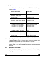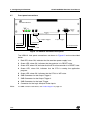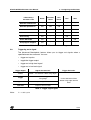
1
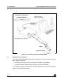
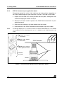
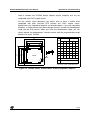
ST92F150-EMU2 Emulator User Manual Release1.3 October 2003 Ref: DOC-ST92F150-EMU2 INSTRUCTIONS FOR USE—WARNING This product is conform to the 89/336/EEC Directive. It complies with the ITE EN55022 standard for EMC emissions and generic 50082-1 (1992 edition) immunity standards. This product is an FCC Class-A apparatus. In a residential environment, it may cause radioelectrical disturbances. In addition, some parts of this emulator are not contained in an outer casing; consequently, it cannot be immune against electrostatic discharges (ESD). It should therefore be handled only in static safe working areas. Please refer to Appendix A: EMC Conformity and Safety Requirements on page 31 for relevant safety information USE IN LIFE SUPPORT DEVICES OR SYSTEMS MUST BE EXPRESSLY AUTHORIZED. STMicroelectronics PRODUCTS ARE NOT AUTHORIZED FOR USE AS CRITICAL COMPONENTS IN LIFE SUPPORT DEVICES OR SYSTEMS WITHOUT THE EXPRESS WRITTEN APPROVAL OF STMicroelectronics. As used herein: 1. Life support devices or systems are those which (a) are intended for surgical implant into the body, or (b) support or sustain life, and whose failure to perform, when properly used in accordance with instructions for use provided with the product, can be reasonably expected to result in significant injury to the user. 2. A critical component is any component of a life support device or system whose failure to perform can reasonably be expected to cause the failure of the life support device or system, or to affect its safety or effectiveness. Table of Contents Chapter 1: 1.1 1.2 1.3 Chapter 2: 2.1 2.2 2.3 Chapter 3: 3.1 3.2 3.3 3.4 3.5 3.6 3.7 3.8 3.9 3.10 3.11 3.12 Chapter 4: 4.1 4.2 4.3 Introduction . . . . . . . . . . . . . . . . . . . . . . . . . . . . . . . . . . . . . . . . . . 5 About the user manuals... ............................................................................. 6 Host PC system requirements ...................................................................... 7 Getting assistance ........................................................................................ 8 Getting Started . . . . . . . . . . . . . . . . . . . . . . . . . . . . . . . . . . . . . . . . 9 Delivery checklist .......................................................................................... 9 Emulator setup instructions ........................................................................ 11 Installing the ST9 software toolchain .......................................................... 15 Configuring the Emulator . . . . . . . . . . . . . . . . . . . . . . . . . . . . . . 17 Selecting the clock source for the ST9 chip ................................................ 17 Selecting the A/D converter analog reference source AVDD ..................... 18 Configuring the P5.0 pin ............................................................................. 19 Mapping the memory space ....................................................................... 19 Resetting the chip ....................................................................................... 23 Interrupting the program execution at any time .......................................... 23 Front panel connections ............................................................................. 24 Triggering out a signal ................................................................................ 25 Analyser probe ............................................................................................ 26 Configuring the timestamp clock ................................................................. 26 Using the performance analysis ................................................................. 27 Configuring peripheral behavior .................................................................. 28 Emulator Functional Discrepancies . . . . . . . . . . . . . . . . . . . . . . 29 Extended function timers ............................................................................ 29 HW0SW1 pin option ................................................................................... 29 Protection register and emulation chip life .................................................. 29 Appendix A: EMC Conformity and Safety Requirements . . . . . . . . . . . . . . . 31 Appendix B: Troubleshooting . . . . . . . . . . . . . . . . . . . . . . . . . . . . . . . . . . . . . 33 B.1 B.2 B.3 B.4 B.5 Emulator reset ............................................................................................ 33 ST9 Visual Debug cannot connect to the emulator .................................... 33 Your emulator stays in reset mode ............................................................. 34 Application memory display issues ............................................................. 34 QFP64/TQFP64 footprint issues ................................................................. 34 3/56 Table of Contents Appendix C: Hardware Layouts . . . . . . . . . . . . . . . . . . . . . . . . . . . . . . . . . . . . 37 C.1 C.2 C.3 Probe board schematics ............................................................................. 37 Probe adapter pinout .................................................................................. 38 Emulator hardware schematics .................................................................. 40 Product Support . . . . . . . . . . . . . . . . . . . . . . . . . . . . . . . . . . . . . . . . . . . . . . . . . 49 Getting prepared before you call............................................................................... Contact list ................................................................................................................ Software updates ...................................................................................................... Hardware spare parts ............................................................................................... 49 50 50 51 Index . . . . . . . . . . . . . . . . . . . . . . . . . . . . . . . . . . . . . . . . . . . . . . . . . . . . . . . . . . . 53 4/56 ST92F150-EMU2 Emulator User Manual 1 1 - Introduction INTRODUCTION Thanks for choosing ST9! This manual will help you get started with the ST9 HDS2V2 emulator kit. When debugging your application, your emulator reproduces the behavior and functionality of the ST9 microcontroller (MCU) in real time, while connected to your application board in place of your MCU. It provides access to the microcontroller’s internal resources (such as registers and memories) and provides you with powerful debugging capabilities such as management of breakpoints and application code trace. Your emulator kit comes with the ST9 V6 Toolchain, which contains all of the necessary resources to help you design, develop and debug ST9 application software. This package includes ST9 Visual Debug — an integrated development environment that allows you to control your emulator and debug your application while it runs in a real environment. Complete information about how to use ST9 Visual Debug can be found in its on-line help. Your ST9 HDS2V2 emulator takes advantage of a dual-microprocessor architecture that allows you to maintain control of the emulator, even if the ST9 application hangs up. Your emulator is composed of three parts (see Figure 1 on page 6): • ST9 Visual Debug integrated development environment, running on your host PC. • The ST9 HDS2V2 mainboard, connected to the host PC via a parallel cable, contains all emulation resources and communicates with the PC via a master microcontroller. • A probe specific to your microcontroller and its package that is connected to the mainboard casing via three flat cables. The probe contains the emulated ST9 microcontroller, which runs the application program using its internal peripherals. The probe is connected to your application board via the ST9 microcontroller's socket. 5/56 1 - Introduction ST92F150-EMU2 Emulator User Manual Emulator Configuration ST9 Visual Debug ST9 HDS2V2 mainboard Probe Adapter for your application board Host PC running ST9 Visual Debug Connects via parallel port ST9 HDS2V2 mainboard Probe Application board Figure 1: ST9 HDS2V2 General Configuration 1.1 About the user manuals... This user manual describes the emulator configurations from the hardware point of view. Here you will find: • Instructions on how to install your emulator hardware and software • Information about configuring your emulator’s hardware features For information about hardware and software intended for use with your emulator, refer to the following documents: 6/56 ST92F150-EMU2 Emulator User Manual 1 - Introduction ST9xxxx-Datasheet — includes information about debugging features that are specific to your microcontroller ST9 V6 Software Toolchain User Manual — build and debug your application software ST9 V6 Software Toolchain - ELF, as9, ld9 and Binutils Reference Manual — detailed information about the ST9 Toolchain ST9 V6 Software Toolchain - gcc9, Libraries and Startup Files Reference Manual — detailed information about the compiler and the provided libraries and startup files ST9 V6 Software Toolchain - gmake Reference Manual — detailed information about recompiling programs with the provided make utility The following conventions are used in this manual: Bold text highlights key terms, phrases and is used when referring to names of dialog boxes, windows and tabs within windows. Bold italic text denotes menu commands (or sequence of commands), options, buttons or checkboxes which you must click in order to perform an action. Italicized text highlights document names, variable strings, column names and field names. Code font designates file names, programming commands, path names and any text you must type. The > symbol is used in a sequence of commands to mean “then”. For example, to open an application in Windows, we would write: “Click Start>Programs>ST9 Tool Chain>....”. 1.2 Host PC system requirements The ST9 HDS2V2 emulator has been designed to work with PCs meeting the following requirements: • One of the following operating systems: Microsoft® Windows® 95, 98, 2000 or NT®. • Intel® Pentium (or compatible) processor with minimum speed of 133 MHz. • Minimum RAM of 32 MB (64 MB recommended). • 50 MB of free hard disk space to install all of the ST9 tools. 7/56 1 - Introduction 1.3 ST92F150-EMU2 Emulator User Manual Getting assistance For more information, application notes, FAQs and software updates on all the ST microcontroller families, check out the CD-ROM or our website: www.stmcu.com For assistance on all ST microcontroller subjects, or for help using your emulator, refer to Product Support on page 49. We’ll be glad to help you! 8/56 ST92F150-EMU2 Emulator User Manual 2 2 - Getting Started GETTING STARTED To help you get started configuring your ST9 HDS2V2 emulator, the following sections provide: Section 2.1 — a check list of components included in your kit Section 2.2 — complete instructions for setting up and connecting your emulator 2.1 Delivery checklist The ST9 HDS2V2 emulator is delivered with the following equipment: Note: • The ST9 HDS2V2 mainboard (in its casing) • One probe (ref.: DB590-A), • Three Yamaichi QFP sockets to solder in place of the ST92F150 MCU package to be used in your application - TQFP64 (14x14) Yamaichi socket (ref.: IC149-084-115-S5) - TQFP100 (14x14) Yamaichi socket (ref.: IC149-184-132-S5) - PQFP100 (20x14) Yamaichi socket (ref.: IC149-084-121-S5) Be aware when designing your application board that Yamaichi socket overall dimensions are larger than device ones. For more information see QFP64/TQFP64 footprint issues on page 34, and the Yamaichi WEB site at address: www.yamaichi.de/Pu/quad_flat_pack/spec/a21-ic149.htm • • Three rigid adapters to fit the target package: - a TQFP64 (14x14) rigid adapter (ref.: DB503) - a TQFP100 (14x14) rigid adapter (ref.: DB502-B) - a PQFP100 (20x14) rigid adapter (ref.: DB329-B) Three flex cable adapters to fit the target package: - a TQFP64 (14x14) flat cable adapter (ref.: DB424) - a TQFP100 (14x14) flat cable adapter (ref.: DB501-B) - a PQFP100 (20x14) flat cable adapter (ref.: DB471) • One 5 V power supply for the ST9 emulator • One parallel cable for connection between the ST9 emulator and the host PC • Three flat cables with ferrites for connection between the probe and emulator mainboard • One analyser probe cable 9/56 2 - Getting Started ST92F150-EMU2 Emulator User Manual Your emulator kit also includes the following documentation: 10/56 • This manual • The “Microcontroller Development Tools” CD-ROM with ST9 Software toolchain versions 4.3x and 6.x. This software package includes: - ST9 Visual Debug software with online help - An assembler, linker, librarian, gmaker and binutils - An ST9 C compiler - The ST9 Visual Programmer (STVP9) software for programming your target devices with and ST9 EPROM Programming Board (EPB) ST92F150-EMU2 Emulator User Manual 2.2 2 - Getting Started Emulator setup instructions The ST9 HDS2V2 emulator is connected via the parallel port to your host PC running ST9 Visual Debug, and to your application board via the probe and provided adapters. A connection flow diagram is shown in Figure 2. Each installation step is described in detail in the following sections. Caution: Before connecting hardware, ensure that neither the emulator nor the application board is powered up. Once you have finished connecting your hardware, you should power up the emulator followed by your application board, in order to prevent damage to the probe. 1 Connect parallel cable 5 Connect mainboard power supply 2 Connect mainboard to probe 3 Set the emulation chip voltage on the probe 4 Connect to your application board 6 Connect application power supply Figure 2: Emulator connection flow diagram 2.2.1 STEP 1: Connect the mainboard to your PC 1 Shutdown and power-off the PC that is to be connected to the emulator. 2 Connect one end of the parallel cable to the mainboard casing’s rear panel 25pin SUB-D connector and the other end to one of the PC’s parallel ports (LPT1 to LPT2). 11/56 2 - Getting Started ST92F150-EMU2 Emulator User Manual Note: The ST9 HDS2V2 emulator supports Centronics (or PC-AT or SPP), ECP and EPP parallel port configurations. Be sure to use the parallel cable provided with the emulator — using a longer parallel cable may cause emulator malfunctions. 2.2.2 STEP 2: Connect the mainboard to the probe The three flat cables must be connected in order as follows (see Figure 3 on page 12 for schematic): 1 The upper cable from mainboard to the J1 connector on probe. 2 The middle cable from mainboard to the J2 connector on probe. 3 The lower cable from mainboard to the J3 connector on probe. Red line on the edge of each flat cable 3 2 1 J3 J2 J1 Figure 3: Connecting the mainboard to the probe 4 12/56 EMC compliancy (optional): In order for the ST9 HDS2V2 emulator to meet the EMC requirements of the European guideline 89/336/EEC, you must follow the guidelines in Appendix A: EMC Conformity and Safety Requirements on page 31 and place the three ferrites provided as shown in Figure 4 on page 13. ST92F150-EMU2 Emulator User Manual 2 - Getting Started Figure 4: Placement of ferrites for EMC conformity STEP 3: Set the emulation chip voltage on the probe Your ST92F150 probe’s emulation chip supports operating voltages of 3.3 and 5 volts. Set the voltage to match that or your application using the W1 jumper on the top of the probe board (see Figure 5). To change the voltage move the jumper to straddle the pins corresponding to the desired voltage. 5 V supply to emulation chip 5V 3V3 W1 jumper 3.3 V supply to emulation chip 5V 3V3 W1 jumper W1 2.2.3 jumper Figure 5: Set voltage for emulation chip 13/56 2 - Getting Started 2.2.4 ST92F150-EMU2 Emulator User Manual STEP 4: Connect to your application board Choose the appropriate socket, rigid adapter or flat cable adapter, depending on the ST92F150 package you want to emulate (TQFP64, TQFP100 or PQFP100). Note: 1 Unpack the Yamaichi QFP socket provided with the probe, setting the cover aside and keeping the screws for step 3. 2 Solder the Yamaichi socket in place of the ST92F150 microcontroller on your application board. 3 Screw the rigid adapter or flat cable adapter onto the socket. 4 Insert the pins of the ST92F150 probe into the adapter (rigid or flat cable). For the rigid adapter, pin “1” is at the cut corner. For the flat cable adapter, pin “1” is labelled on the adapter. For the ST92F150 probe, pin “1” is labelled on the component-side of the probe. 1 Unpack the socket and adapter 3 Screw rigid adapter onto socket ST92F150 probe J1 2 Solder the socket to the application board pin 1 Protection (not used) Rigid adapter Socket Application board Figure 6: :Connecting the probe to your application board 14/56 J2 J3 ST92F150-EMU2 Emulator User Manual 2.2.5 2.2.6 2 - Getting Started STEP 5: Connecting the power supply 1 Connect the power supply provided with the emulator to the mainboard rear panel. 2 Power up the ST9 HDS2V2 emulator from the ON/OFF switch located on the rear panel. The three LEDs labelled Power, Emulator Reset and ST9 Reset on the front panel should then light up (see Figure 12 on page 24). STEP 6: Powering up 1 Connect the power supply for your application board. 2 Power up your application board. If the voltage setting for your emulation chip corresponds to that of your application, the Green LED (LD1) on the probe board will be lit. If the voltage settings do not match, the Red LED (LD2) on your probe board will be lit. If this happens, power off your application and then your ST9 HDS2V2 mainboard. Confirm the voltage of your application and set the voltage for the emulation chip (3.3 or 5V) as described in STEP 3: Set the emulation chip voltage on the probe on page 13. Warning: Always power on your ST9 HDS2V2 emulator first, then power up your application board. When powering off, always power off your application board first, then power off your emulator. NEVER have your application board under power while the emulator is powered off— this will cause serious damage to the emulator. 2.3 Installing the ST9 software toolchain Your ST9 HDS2V2 emulator comes with the “Microcontroller Development Tools” CD-ROM which contains the ST9 software toolchain. Note: Windows® 2000 and NT® users must have administrator privileges to install the software toolchain. To install ST9 Visual Debug or the entire ST9 Software Toolchain, follow these steps: 1 Close all other open applications on your Windows desktop. 15/56 2 - Getting Started ST92F150-EMU2 Emulator User Manual 2 Insert the “Microcontroller Development Tools” CD-ROM into your CD-ROM drive. The autorun feature will open up a welcome screen on your PC. If the autorun feature does not work, use Windows® Explorer to browse to the CDROM’ s root folder, and double-click on Welcome.exe. A screen will appear listing the different families of ST microcontrollers. 3 Use your mouse to place the cursor over the ST9 option. Then choose ST9 Toolchain V6, which contains ST9 Visual Debug, as well as the ST9 Assembler-Linker software and other tools. 4 The install wizard will be launched. Follow the instructions that appear on the screen. A tutorial on how to start using ST9 Visual Debug is contained in the ST9 V6 Software Toolchain User Manual, available in PDF format on the “MCU on CD” CD-ROM. 16/56 ST92F150-EMU2 Emulator User Manual 3 - Configuring the Emulator 3 CONFIGURING THE EMULATOR 3.1 Selecting the clock source for the ST9 chip You can select one of three clock sources for ST92F150 emulation chip: • A quartz (not provided), to be located on the probe between C4 and C5. • A 4 MHz is provided by the emulation chip (PLD 885-10). • The target TTL clock source, located on your application board. The clock source selection is made with the five solder points (G3, G4, G5, G6, G7) and the W5 jumper. Clock Source G4 G5 G6 G7 G8 W5 on probe quartz (XT1) N Y Y N Y - on probe 4 MHz oscillator Y N N Y N P-OSC external TTL clock source Y N N Y N T-OSC Table 1: Clock source solder points and jumper settings * “Y” means the solder point’s contacts must be soldered together, “N” means no contact. When delivered, the on-probe 4 MHz oscillator is connected as the emulator clock source. This means that the contacts of both the G4 and G7 solder points are connected with a thin copper wire and the W5 jumper is in the P-OSC position.To remove the connection between the contacts of the G4 and G7 solder points, simply scratch the thin copper wire between the contacts of each solder point. External TTL clock On-probe 4 MHz Oscillator W5 W5 T-OSC T-OSC jumper P-OSC jumper P-OSC Figure 10: Clock selection jumper Note: When using the TTL clock source on your application board during emulation, the clock source must be connected to the OSCIN pin of the MCU socket on your application board. However, when you disconnect the probe and install your MCU on the socket to run your application, you must reconnect the clock source to the socket’s OSCOUT pin. For specific 17/56 3 - Configuring the Emulator ST92F150-EMU2 Emulator User Manual connection information regarding the MCU’s Clock Control Unit, refer to the ST92F150 Datasheet. 3.2 Selecting the A/D converter analog reference source AVDD You can supply AVDD either from the emulator probe power supply or from your application using the AVDD pin of ST92F150. G2 G3 AVDD from emulator probe Y N AVDD from application (AVDD pin) N Y Table 2: AVDD supply selection solder points * “Y” means the solder point’s contacts must be soldered together, “N” means no contact. When delivered, AVDD is supplied by the emulator probe—i.e. the G2 solder point contacts have been connected with a thin copper wire. To remove connection, scratch the thin copper wire between the two contacts. 18/56 ST92F150-EMU2 Emulator User Manual 3.3 3 - Configuring the Emulator Configuring the P5.0 pin You can choose between configuring the P5.0 pin for use as a port or for use with the WAITn function. Figure 11 below shows how to set jumpers W2 and W3 on your probe for either configuration Jumper positions WAITN W3 W4 P5.0 I/O Jumper positions WAITN W3 W4 Jumper setting for WAITn function Jumper setting for use as an I/O port P5.0 I/O Figure 11: P5.0 pin configurations 3.4 Mapping the memory space 3.4.1 Internal memory The actual memory located inside an ST9 chip (RAM, EEPROM and/or FLASH) is called internal memory. When we say that we are using internal memory, it means that we are in fact using the memory internal to the target ST9 device located on the emulation probe. Doing this, however, greatly limits the emulator debugging capabilities, as described in Section 3.4.3. 3.4.2 System memory Some of the ST9 chip’s internal memory, such as RAM and FLASH, cannot be used for emulation purposes. In the emulator, emulation RAM replaces some ST9 internal memory types, and enables you to debug an application program by 19/56 3 - Configuring the Emulator ST92F150-EMU2 Emulator User Manual modifying the code whenever an error is encountered. This emulation memory is located on the emulator’s mainboard and is called system memory. 3.4.3 FLASH and EEPROM memory The emulator allows you to define the FLASH and EEPROM memory mapping as either internal or system. Whether it is FLASH or EEPROM, all the memory must be mapped in the same location, internal or system. When this memory is mapped as internal, the emulator does not have the same debug information available as it would have when using system memory. When using internal memory, the values read from it cannot be accurately determined while the chip is running. As a result, the use of advanced breakpoints that read conditional values from this memory is forbidden. Another consequence is that the values displayed in the Trace window, which are being read from internal memory while the application is running, are not accurate. To indicate this in the Trace window, the values appear in grey text with a questionmark (“?”) at the beginning and end of the inaccurate data. However, once the application has stopped executing, the correct values can be dumped to the Memory window. During the main development stage, you should map the FLASH memory as system, which allows you to use all of the emulator’s debugging features. However, when you want to test FLASH programming, you should map the FLASH memory to internal and program the emulation chip’s FLASH memory with your application (use ISP or your boot-program located in RAM). After executing the application, you can display the emulation chip’s FLASH memory in ST9 Visual Debug’s Memory window (select View>Memory from the main menu bar). Note: If you program the emulation chip on the probe using ISP, the emulator must be running (executing a loop program). Usually the EEPROM memory will be mapped to internal. Nevertheless if you want to put a condition on a value read in the EEPROM memory, or trace the values read in it, you can map it as system memory. 20/56 ST92F150-EMU2 Emulator User Manual 3.4.4 3 - Configuring the Emulator User memory You can map external memory segments in two different ways: • either you can use the on-emulator memory to emulate those segments. In this case, you define it as system memory, • or you can use the memory located on your application board. In this case, you define it as user memory. In both cases all emulation features (such as breakpoints, trace, memory window, memory access control) are available. Some differences in behavior must however be considered. When mapping external segments as system memory, the following must be taken into account: • When external memory is accessed through port 0 or port 1, the emulator will not detect if the ports are incorrectly configured with alternate functions to access external memory. If the configuration is not correct, your application program may run using system memory, but it will not run correctly with user memory or with the chip itself. • The emulator will function at its maximum operating speed without requiring wait states to access system memory, whereas wait states may be required for the chip to access your application memory. To avoid problems with external memory interface configuration, you should debug your application program in two steps: 3.4.5 1 The first step is to debug your program using the emulation memory. 2 The second step is to debug your program with the application memory to ensure that ports and access configurations are correct. Memory location In most cases, configuration is done by memory segment. All MMU bits are available on the ST92F150 emulation chip, however none are available as port P2 alternate function on the ST92F150 target device. So, with the ST92F150-EMU2 emulator, the entire 4 MB of memory space can be used as system memory but only 64 KB can be used as user memory. This has been done to support future versions of ST92F150 devices. All ST92F150 device mappings 21/56 3 - Configuring the Emulator ST92F150-EMU2 Emulator User Manual are available, plus an additional mapping — the “ST92F150 emulator” mapping shown inTable 3. ST92F150 memory areas Memory types segment 00h: @0000h-001Fh system segment 00h: @0020h-FFFFh segment 01h: @0000h-FFFFh system, internal or non-existent segments 02h, 03h system or non-existent segments 04h-1Fh system, user or non-existent segment 20h: @0000h-03FFh (16K-RAM) system or non-existent segment 21h reserved segments 22h from 0000h to 03FFh from 1000h to 101Fh from 4000h to 401Fh from 8000h to 8FFFh from 9000h to 90FFh from C000h to CFFFh from D000h to D0FFh segments 23h from 0000h to 1F7Fh from 1F80h to 1FFFh (1K-eeprom) (control reg.) (control reg. (4K-F4) (256:status) (4K-F5) (256:status) (Test-FLASH) (FLASH-OTP) segments 24h-3Fh internal, system or non-existent internal or non-existent internal or non-existent internal, system or non-existent internal internal, system or non-existent internal internal or system internal or system system, user or non-existent Table 3: Choosing the appropriate memory types for your application 3.4.6 Controlling the memory accesses The memory mapping feature in ST9 Visual Debug allows you to define the access characteristics of the memory: non-existing, read only or read/write. When not specified in the map, the memory areas are considered as non-existent, and any access to that memory zone by your application will generate an error message. 3.4.7 Mapping the memory space Mapping the memory space can be performed by using the Memory Mapping window of ST9 Visual Debug, accessible by selecting Emulator>Memory Mapping from the main menu bar. 22/56 ST92F150-EMU2 Emulator User Manual 3.4.8 3 - Configuring the Emulator Mapping granularity You can define the memory mapping with a granularity of 32 bytes. 3.5 Resetting the chip 3.5.1 Performing a software reset The CHIP RESET command allows you to send a reset to the ST9 device and stops the application on the reset vector. 3.5.2 Performing a hardware reset You can send a reset to the ST9 device by applying a 0 level on the ST9 RESETn pin (on the emulator probe adapter). If your application is running, the reset will be taken into account as a normal device reset and the program will keep on running from the reset vector address without any disturbance from the emulator. If your application program is not running, the reset is ignored. If maintained when you will run our program, the reset will be taken into account. 3.6 Interrupting the program execution at any time Loading a program into the emulator allows you to execute it and stop it whenever you need to. You can stop the program execution at any time with the debugger— refer to the ST9 Visual Debug on-line help. If you perform a program stop in ST9 Visual Debug while the ST9 is in HALT mode, a chip reset is applied, and the ST9 will stop on the reset vector. The HALT instruction will be recorded in the Trace buffer. If you perform a program stop in ST9 Visual Debug while the ST9 is in STOP mode, you will wake up the ST9. If you perform a Continue or a Step command afterwards, the ST9 will return to STOP mode. The only real way to exit STOP mode and continue executing your program is to have the STOP mode exit condition satisfied (i.e. reception of a wake-up input signal). 23/56 3 - Configuring the Emulator 3.7 ST92F150-EMU2 Emulator User Manual Front panel connections 6 - Output Triggers 1- Red LED 2- Green LED 7- Input Trigger 5 - Green LED 4- Green LED 9- Analyser Probe 3- Green LED Figure 12: HDS2V2 mainboard front panel The HDS2V2 front panel connections are shown in Figure 12 and are described below: Note: 24/56 1 Red LED, when ON, indicates that the emulator power supply is on. 2 Green LED, when ON, indicates that the emulator is in RESET state. 3 Green LED, when ON, indicates that the ST9 microcontroller is in RESET state. 4 Green LED, when ON, indicates that the ST9 is running the application program. 5 Green LED, when ON, indicates that the ST9 is in WFI state. 6 SMB Connector for the Output Trigger 1. 7 SMB Connector for the Output Trigger 2. 8 SMB Connector for the Input Trigger. 9 Connector for the Logic Analyser Probe inputs. For SMB connector references, see Product Support on page 49. ST92F150-EMU2 Emulator User Manual LED activity / 3 - Configuring the Emulator Power Emulator Reset ST9 Reset Run Wait Emulator switched off - - - - - Emulator powered on ON ON ON - - Emulator reset ON ON ON - - ST9 reset ON - ON - - ST9 running ON - - ON - ST9 in WFI mode ON - - - ON ST9 program stopped ON - - - - Emulator state Table 4: Front panel LEDs and their meanings 3.8 Triggering out a signal The Advanced Breakpoints feature allows you to trigger out signals when a specified event has occurred. You can: • trigger out a pulse • toggle the trigger output • trigger out a high level signal • trigger out a low level signal Trigger Signal Signal characteristic Pulse Width = 2*T between 2 DSn rising edges Toggle Invert the level of the trigger on a DSn rising edge High level Output a high TTL level Low level Output a low TTL level Trigger Activation On the 3rd internal Data Strobe rising edge after the event Table 5: Trigger signal types Note: T = 1 CPU cycle. 25/56 3 - Configuring the Emulator 3.9 ST92F150-EMU2 Emulator User Manual Analyser probe The analyser probe, a SUBD9 connector located on the front panel of the emulator main board casing, provides eight external probe inputs that can be used as: • possible advanced breakpoint events • bus signals in the trace They are synchronized with DSn and respect the 5 V TTL input levels: VIL = 0.8 V, VIH = 2 V. The analyser probe cable consists of 8 colored wires that correspond to specific pin numbers, as shown below in Table 6. Input Number Wire Color 0 Brown 1 Red 2 Orange 3 Yellow 4 Green 5 Blue 6 Violet 7 Grey Table 6: Pin/wire color correspondence on analyser probe 3.10 Configuring the timestamp clock The Timestamp clock can be configured using ST9 Visual Debug. Open the Trace window by selecting, from the main menu, View>Trace. With your cursor in the Trace window, right-click to obtain the Trace contextual menu, and then select 26/56 ST92F150-EMU2 Emulator User Manual 3 - Configuring the Emulator Emulator Commands>Set Timestamp Clock. The Timestamp Clock dialog box, shown in Figure 13 on page 27, will appear. Figure 13: Timestamp clock source dialog box The clock source available for timestamp clock depends upon the ST92F150 clock source selected (see Section 3.1 on page 17): 3.11 • When using the on-probe quartz, only use the fixed 20 MHz reference is available for use as the timestamp clock. No configuration is required—the timestamp clock is set by default to Internal. • When using the on-probe oscillator or the external TTL clock source from your application, you can select either: - a fixed 20 MHz reference, which is the Internal option in the Timestamp Clock dialog box. - or the ST9 OSCIN source—in this case, you must check the External radio button of the dialog box shown in Figure 13 and enter the frequency of the external OSCIN source. Using the performance analysis For details, please refer to ST9 Visual Debug’s on-line help. Note, however, that the performance analysis uses both Advanced Breakpoints and the Trace. As a consequence, when analyzing the performance of your code you can use neither the Advance Breakpoints feature nor the Trace. When the performance analysis is finished, your Advanced Breakpoint and Trace configurations will be restored. 27/56 3 - Configuring the Emulator 3.12 ST92F150-EMU2 Emulator User Manual Configuring peripheral behavior Some peripherals can be configured so that they are stopped, or continue to run, when the program stops during an ST9 Visual Debug session (i.e. when a breakpoint is encountered, etc.). In ST9 Visual Debug, configure peripherals by selecting, Emulator>Peripheral Control... from the main menu. The Peripherals Control window displays how the emulated device’s peripherals will behave (i.e. either run or stop) when the program execution is stopped. By default, the peripherals are configured to Run—so that they will continue to run even if the program execution is stopped. For the ST92F150, six control bits are available for this functionality, so the following six individual selections have been chosen for configuration: Note: 28/56 • Watchdog Timer - When this peripheral is configured as standard timer, the Run option allows the timer to continue to run even when program execution has stopped. The Stop option will freeze the timer when the program is stopped. However, when configured as watchdog, this timer is automatically disabled whenever the program is stopped, regardless of the option chosen. • Multifunction Timer 0- If the Stop option is chosen, timer counting is disabled when the program is stopped. • Multifunction Timer 1 - If the Stop option is chosen, timer counting is disabled when the program is stopped. • Extended Function Timer 0 - If the Stop option is chosen, timer counting is disabled when the program is stopped. • Extended Function Timer 1 / CAN 0 - If the Stop option is chosen, both the timer counting and the CAN 0 is disabled when the program is stopped. • J1850 / CAN 1 - If the Stop option is chosen, both the timer counting and the CAN 0 is disabled when the program is stopped. The A/D conversion is always stopped when the program is stopped by ST9 Visual Debug. It restarts when the user program starts running again. The Watchdog Timer is always stopped while the program is stopped by ST9 Visual Debug. It continues running when your program starts running again. ST92F150-EMU2 Emulator User Manual 4 - Emulator Functional Discrepancies 4 EMULATOR FUNCTIONAL DISCREPANCIES 4.1 Extended function timers The two Extended Function Timers work correctly on the emulator but the related registers cannot be read using the Registers Windows, nor through the Watch Window. You should not display the alternate counter contents using ST9 Visual Debug. If required, use the following workaround: When you need to verify the value of the counter, add in your program instructions that copy the alternate counter contents in two working registers (one for the Alternate Counter High byte, one for the Alternate Counter Low byte). Remember that the MSB must be read first. Display the working registers window to check the counter values. 4.2 HW0SW1 pin option A 10 KΩ pull-up resistor has been added to the emulator. When the emulator is not connected to your application board, the default option is the software watchdog reset. On your application board, if you want to force a hardware watchdog reset, you should connect the HW0SW1 pin directly to GND. 4.3 Protection register and emulation chip life The emulator uses the OTP area in the same way that the target MCU does. This register can be written to only once. Your emulator uses a chip similar to the target MCU. For the FLASH and EEPROM memories, this means that write cycles in these areas are limited. If, after a while, writing to memory is no longer possible for the FLASH or EEPROM areas, the BGA144 emulation chip will have to be changed. (Note that loading application software in system memory does not write to the FLASH area). 29/56 4 - Emulator Functional Discrepancies 30/56 ST92F150-EMU2 Emulator User Manual ST92F150-EMU2 Emulator User Manual Appendix A: EMC Conformity and Safety Requirements APPENDIX A: EMC CONFORMITY AND SAFETY REQUIREMENTS This emulator respects the EMC requirements of the European guideline 89/336/ EEC under the following conditions: • Any tester, equipment, or tool used at any production step or for any manipulation of semiconductor devices must have its shield connected to ground. • All ferrites provided with the emulator must be attached as described in the hardware installation instructions of the relevant user manual(s). • Your emulator must be placed on a conductive table top, made of steel or clean aluminum, grounded through a ground cable. All manipulation of finished goods must be done at such a grounded worktable. • The worktable must be free of all non-antistatic plastic objects. • It is recommended that you wear an antistatic wrist or ankle strap, connected to the antistatic floor covering or to the grounded equipment. • If no antistatic wrist or ankle strap is worn, before each manipulation of the powered-on emulator, you must touch the surface of the grounded worktable. • It is recommended that antistatic gloves or finger coats be worn. • It is recommended that nylon clothing be avoided while performing any manipulation of parts. 31/56 Appendix A: EMC Conformity and Safety Requirements 32/56 ST92F150-EMU2 Emulator User Manual ST92F150-EMU2 Emulator User Manual Appendix B: Troubleshooting APPENDIX B: TROUBLESHOOTING B.1 Emulator reset This command performs a reset of the ST9 device and all emulator configurations such as mapping, breakpoints, trace and timestamp. Use it only when there is a problem with the emulator itself or if the emulator was powered off without closing ST9 Visual Debug. The emulator reset behaves like a hardware reset of the emulator. The application loaded in the debugger is automatically closed. B.2 ST9 Visual Debug cannot connect to the emulator Verify that the whole installation has been performed correctly. Refer to the set up procedure, Section 2.2 on page 11. If ST9 Visual Debug still cannot connect to the emulator, confirm that: • You have selected the appropriate parallel port. If the parallel cable is not connected to LPT1 but to LPT2, change the port name (refer to the ST9Visual Debug’s on-line help). • You are using the parallel cable delivered with your emulator. Do not use a longer cable. • You have not connected the cable to a serial interface of the PC, this could damage the emulator. • The cable is connected directly to the DB-25 female connector of the PC parallel port. No additional cables or switchboxes between the PC and the board should be installed. • If the PC parallel port connector is not a DB25-type connector (e.g.: such as miniature plug or receptacle 36-pin ribbon type connector as specified in IEEE1284-1994 standard), use the adapter provided with your PC. Note that the different connector type indicates that your PC parallel port should be IEEE-1284 compliant: check that proper mode (Centronics Compatible Mode) is installed in your PC’s BIOS. • If a dongle (hardware key required by some PC software) is already connected to the PC parallel port, it should not interfere with the emulator. However, if you notice a malfunction, you should remove the dongle(s) and try to establish the connection again. 33/56 Appendix B: Troubleshooting B.3 ST92F150-EMU2 Emulator User Manual Your emulator stays in reset mode Your emulator is connected to your application board. When you try to run your program, you observe that the LED ST9 Reset remains switched on. When you stop your program, the program counter points to the reset vector. B.4 • Verify that your application board is powered up. When your emulator is connected to your application board, it can detect whether your application board is powered up or not. If not, the emulator will remains in reset state. • Verify that the reset line on your application board is not pulled low. When your application board is reset, the ST9 chip will remain in reset also, when you try to run your program. Application memory display issues • You should not display contents of memories such as FIFO, LIFO... Otherwise you could lose the synchronization of your memory when the display reads its contents. The same problems can also occur when the memory area you selected to display in the Memory window overlaps such memories. For example, your FIFO is located at address 0x01C000, some RAM is located at address 0x018000 to 0x01BFFF, and you display the memory space from 0x01BE00. Depending on the size of your Memory window, the display can show memory contents up to 0x01C0ff and cause problems in your FIFO. In that case, it is advised to take special care with the size of the Memory window. B.5 • If you are asking for a display of external memory mapped as user memory, you have to configure the external memory interface using EMR1, EMR2, and P0Cx, P1Cx, P2Cx registers as your final software should do before asking for the dump. • When using the Memory window, the ST9 wait states are configured differently than when you are running your program. Two wait states on Data Strobe are automatically selected. When running your program, the number of wait states you choose is used. QFP64/TQFP64 footprint issues Some of the emulated devices have a TQFP64 footprint and require you to solder a Yamaichi QFP64 socket onto your application board. However, be aware that you may encounter problems owing to the fact that the Yamaichi QFP64 sockets 34/56 ST92F150-EMU2 Emulator User Manual Appendix B: Troubleshooting used to connect the TQFP64 device adapter require footprints that are not compatible with TQFP copper traces. For this reason, when designing your board, plan to have a double trace compatible with both Yamaichi QFP sockets and TQFP copper traces. Specifications for compatible footprints are provided below. If you use compatible footprints, a single printed circuit board design will serve for both the development stage and the final product. When you finish the development stage, you can simply replace the development Yamaichi socket with the programmable target device in an actual TQFP64 SK mm E inches Dim Min E1 E3 e Typ Max Min Typ Max B 0.35 0.45 0.50 0.014 0.018 0.020 E 20.80 E1 0.819 14.00 0.551 E3 E E1 SK E3 11.90 12.00 12.10 0.468 0.472 0.476 B e 0.75 0.80 0.85 0.029 0.031 0.033 SOCKET SK* DETAIL 26 1.023 Number of Pins N 64 (4x16) * SK: Plastic socket overall dimensions. Figure 14: TQFP64 Device and Emulation Probe Compatible Footprint 35/56 Appendix B: Troubleshooting 36/56 ST92F150-EMU2 Emulator User Manual ST92F150-EMU2 Emulator User Manual Appendix C: Hardware Layouts APPENDIX C: HARDWARE LAYOUTS C.1 Probe board schematics SOCKET FBGA144 TP1 TP2 TP3 TP4 RS9 V4 V5 C1 U6 RS10 U9 RS11 U13 U15 U16 EMBASE MALE DROIT 80 Pts C2 EMBASE MALE DROIT 80 Pts EMBASE MALE DROIT 80 Pts Figure 15: Probe board top-side schematic 37/56 Appendix C: Hardware Layouts ST92F150-EMU2 Emulator User Manual U11 FACE 1 FACE 6 Protection Figure 16: Probe board bottom-side schematic with side-view C.2 Probe adapter pinout 69 70 68 46 67 45 44 43 ST92F150 Male Adapter 2 24 26 25 91 92 1 23 Figure 17: Probe device adapter pin placements 38/56 ST92F150-EMU2 Emulator User Manual Appendix C: Hardware Layouts Pin No. Pin Name Pin No. Pin Name Pin No. Pin Name 1 P9.3 32 P2.2 63 P6.3 2 P9.4 33 P2.3 64 P6.4 3 P9.5 34 P2.4 65 P6.5 4 P9.6 35 P2.5 66 VPWO 5 P9.7 36 P2.6 67 P8.0 6 P5.0 37 P2.7 68 P8.1 7 P5.1 38 VSS 69 P8.2 8 P5.2 39 VDD (target) 70 P8.3 9 P5.3 40 P1.0 71 P8.4 10 P5.4 41 P1.1 72 P8.5 11 P5.5 42 P1.2 73 P8.6 12 P5.6 43 RXCAN 74 P8.7 13 P5.7 44 TXCAN 75 AVDD (target) 14 P4.0 45 P1.3 76 VSS 15 P4.1 46 P1.4 77 P7.0 16 P4.2 47 P1.5 78 P7.1 17 P4.3 48 P1.6 79 P7.2 18 P4.4 49 P1.7 80 P7.3 19 P4.5 50 DSn 81 P7.4 20 P4.6 51 ASn 82 P7.5 21 P4.7 52 P0.0 83 P7.6 22 P3.1 53 P0.1 84 P7.7 23 P3.2 54 P0.2 85 VSS 24 P3.3 55 P0.3 86 VDD (target) 25 P3.4 56 P0.4 87 OSCIN (target) 26 P3.5 57 P0.5 88 RESETn 27 P3.6 58 P0.6 89 HW0SW1 28 P3.7 59 P0.7 90 P9.0 29 RWN 60 P6.0 91 P9.1 30 P2.0 61 P6.1 92 P9.2 31 P2.1 62 P6.2 Table 7: Probe adapter pinout 39/56 Appendix C: Hardware Layouts C.3 ST92F150-EMU2 Emulator User Manual Emulator hardware schematics Figure 18: Probe synoptic schematic 40/56 ST92F150-EMU2 Emulator User Manual Appendix C: Hardware Layouts Figure 19: Probe/mainboard connectors 41/56 Appendix C: Hardware Layouts ST92F150-EMU2 Emulator User Manual Figure 20: Mainboard/probe interface schematic 42/56 ST92F150-EMU2 Emulator User Manual Appendix C: Hardware Layouts Figure 21: Mainboard/probe interface 43/56 Appendix C: Hardware Layouts ST92F150-EMU2 Emulator User Manual Figure 22: Control logic schematic 44/56 ST92F150-EMU2 Emulator User Manual Appendix C: Hardware Layouts Figure 23: Emu chip and adapter schematic 45/56 Appendix C: Hardware Layouts ST92F150-EMU2 Emulator User Manual Figure 24: Emu chip and adapter schematic 46/56 ST92F150-EMU2 Emulator User Manual Appendix C: Hardware Layouts Figure 25: Decoupling schematic 47/56 Appendix C: Hardware Layouts 48/56 ST92F150-EMU2 Emulator User Manual ST92F150-EMU2 Emulator User Manual Product Support PRODUCT SUPPORT If you experience any problems with this product or if you need spare parts or repairs, contact the distributor or ST sales office where you purchased the product. In addition, at our internet site mcu.st.com, you will find documentation, software downloads and user discussion groups to help answer questions and stay up to date with the latest product developments. Getting prepared before you call Collect the following information about the product before contacting ST or your distributor: 1 Name of the company where you purchased the product. 2 Date of purchase. 3 Order Code: Refer to the side your emulators box. The order code will depend on the region in which is was ordered (i.e. the UK, Continental Europe or the USA). 4 Serial Number: The serial number is located on the rear panel of the ST9 HDS2V2 mainboard casing and is also listed on the Global Reference card provided with the emulator kit. 5 Hardware and firmware versions: The they can be found by opening an ST9 Visual Debug session, entering the debug context and selecting Help>About from the main menu. 6 Target Device: The sales type of the ST microcontroller you are using in your application. 49/56 Product Support ST92F150-EMU2 Emulator User Manual Contact list North America Canada and East Coast STMicroelectronics Lexington Corporate Center 10 Maguire Road, Building 1, 3rd floor Lexington, MA 02421 Phone: (781) 402-2650 Mid West STMicroelectronics 1300 East Woodfield Road, Suite 410 Schaumburg, IL 60173 Phone: (847) 585-3000 West coast STMicroelectronics, Inc. 1060 E. Brokaw Road San Jose, CA 95131 Phone: (408) 452-8585 Note: For American and Canadian customers seeking technical support the US/Canada is split in 3 territories. According to your area, contact the appropriate sales office from the list above and ask to be transferred to an 8-bit microcontroller Field Applications Engineer. Europe France +33 (0)1 47 40 75 75 Germany +49 89 46 00 60 U.K. +44 162 889 0800 Asia/Pacific Region Japan +81 3 3280 4120 Hong-Kong +85 2 2861 5700 Sydney +61 2 9580 3811 Taipei +88 6 2 2378 8088 Software updates You can get software updates from the ST Internet web site mcu.st.com. For information on firmware and hardware revisions, call your distributor or ST using the contact list given above. 50/56 ST92F150-EMU2 Emulator User Manual Product Support Hardware spare parts Your emulator kit contains the hardware you need to set it up and connect it to your application. However, some components can be bought separately if you need additional ones. You can order extra components, such as sockets and adapters, from STMicroelectronics’ sales offices, from the component manufacturer or from a distributor. Sockets You will find complete documentation and ordering information for P/TQFP sockets from Yamaichi, Ironwood, CAB and Enplas at: www.yamaichi.de www.ironwoodelectronics.com www.cabgmbh.com www.enplas.com 51/56 Product Support 52/56 ST92F150-EMU2 Emulator User Manual Index A A/D convertor analog reference source ........ 18 adapter QFP....................................................... 14 C clock source for emulation chip..................... 17 connection problems ..................................... 33 E EMC compliancy ferrites ................................................... 12 requirements for.................................... 31 emulator chip reset ........................................ 23, 33 configuring ............................................ 17 configuring P5.0 pin .............................. 19 connecting to probe .............................. 12 connection problems............................. 33 front panel description........................... 24 hardware provided .................................. 9 installing the hardware .......................... 11 LED description..................................... 24 mainboard ............................................... 5 probe....................................................... 5 selecting AVDD source ......................... 18 selecting clock source........................... 17 setting supply voltage to chip................ 13 triggers .................................................. 25 F ferrites placement of ......................................... 13 finished goods manipulation of...................................... 31 safety requirements .............................. 31 H hardware setting up .............................................. 11 I inputs from analyser probe...............................26 from input trigger ...................................24 installation emulator hardware.................................11 J jumper(s) clock source...........................................17 P5.0 pin configuration ............................19 voltage selection....................................13 L LEDs emulator status ......................................15 status description...................................24 voltage setting .......................................15 M memory mapping...........................................19 defining user memory ............................20 emulation chip .......................................21 P P5.0 pin configure as I/O port or WAITN .............19 parallel port connections................................11 trouble shooting .....................................33 peripherals configuring .............................................28 display data channel..............................28 watchdog timer ......................................28 powering up device sequence....................................15 important warning ..................................15 probe connecting to application .......................14 connecting to emulator ..........................12 53/56 Index Q QFP64/TQFP64 footprint issues ................... 34 S safety requirements ...................................... 31 software CD-ROM ............................................... 10 updates ................................................. 50 solder points clock source .......................................... 17 P-AVDD and T-AVDD ........................... 18 ST9+ V6 Software Toolchain installing ................................................ 15 ST9+ Visual Debug installing ................................................ 15 performance analysis function .............. 27 54/56 support web support .............................................8 T text conventions...............................................6 timestamp clock configuration .......................26 triggers...........................................................25 modes....................................................25 troubleshooting ..............................................33 V voltage selection ............................................13 W working environment recommendations........31 ST92F150-EMU2 Emulator User Manual - 55/56 Information furnished is believed to be accurate and reliable. However, STMicroelectronics assumes no responsibility for the consequences of use of such information nor for any infringement of patents or other rights of third parties which may result from its use. No license is granted by implication or otherwise under any patent or patent rights of STMicroelectronics. Specifications mentioned in this publication are subject to change without notice. This publication supersedes and replaces all information previously supplied. 5 STMicroelectronics products are not authorized for use as critical components in life support devices or systems without the express written approval of STMicroelectronics. 6 The ST logo is a registered trademark of STMicroelectronics 2003 STMicroelectronics - All Rights Reserved. Purchase of I2C Components by STMicroelectronics conveys a license under the Philips I2C Patent. Rights to use these components in an I2C system is granted provided that the system conforms to the I2C Standard Specification as defined by Philips. STMicroelectronics Group of Companies Australia - Brazil - Canada - China - Finland - France - Germany - Hong Kong - India - Israel - Italy - Japan Malaysia - Malta - Morocco - Singapore - Spain - Sweden - Switzerland - United Kingdom - U.S.A. http://www.st.com 56