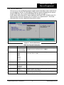
1
1.04
ZFx86™
Phoenix BIOS
User’s Supplement
Version 1.04ah (Pre-Release)
April 16, 2001
© 2001 ZF Micro Devices, Incorporated
P/N 9100-0066-01
MachZ BIOS User’s
Manual Supplement
THIS DOCUMENT AND THE INFORMATION CONTAINED THEREIN IS PROVIDED “AS-IS”
AND WITHOUT A WARRANTY OF ANY KIND. YOU, THE USER, ACCEPT FULL RESPONSIBILITY FOR PROPER USE OF THE MATERIAL. ZF MICRO DEVICES, INC. MAKES NO REPRESENTATIONS OR WARRANTIES THAT THIS DATA BOOK OR THE INFORMATION
CONTAINED THERE-IN IS ERROR FREE OR THAT THE USE THEREOF WILL NOT
INFRINGE ANY PATENTS, COPYRIGHT OR TRADEMARKS OF THIRD PARTIES. ZF MICRO
DEVICES, INC. EXPLICITLY ASSUMES NO LIABILITY FOR ANY DAMAGES WHATSOEVER
RELATING TO ITS USE.
LIFE SUPPORT POLICY
ZF MICRO DEVICES PRODUCTS ARE NOT AUTHORIZED FOR USE AS CRITICAL COMPONENTS IN LIFE SUPPORT DEVICES OR SYSTEMS WITHOUT THE EXPRESS WRITTEN
APPROVAL OF THE PRESIDENT AND GENERAL COUNSEL OF ZF MICRO DEVICES, INC.
As used herein:
1. Life support devices or systems are devices or systems which, (a) are intended for surgical
implant into the body, or (b) support or sustain life, and whose failure to perform when properly
used in accordance with instructions for use provided in the labeling, can be reasonably
expected to result in a significant injury to the user.
2. A critical component is any component of a life support device or system whose failure to perform can be reasonably expected to cause the failure of the life support device or system, or to
affect its safety or effectiveness.
(c)2001 ZF Micro Devices, Inc. All rights reserved.
ZFx86, FailSafe FailSafe Boot ROM, Z-tag ZF-Logic, InternetSafe, OEMmodule SCC, ZF SystemCard, ZF FlashDisk-SC, netDisplay, ZF 104Card, ZF SlotCard, and ZF Micro Devices logo
are trademarks of ZF Micro Devices, Inc. Other brands and product names are trademarks of
their respective owners.
P/N 9100-0066-01
ii
© 2001 ZF Micro Devices, Incorporated
MachZ BIOS User’s
Manual Supplement
1. Introduction to the ZFx86 BIOS .......................................................................................... 1
2. Features ................................................................................................................................ 1
2.1. ZFx86 BIOS Set Contents.............................................................................................. 2
3. Installation ............................................................................................................................ 2
3.1. Installation Using amdflash.exe ..................................................................................... 2
3.2. Installation Using the Dongle ......................................................................................... 4
4. BIOS Setup ........................................................................................................................... 4
4.1. Main ............................................................................................................................... 4
4.2. Advanced ....................................................................................................................... 4
4.3. Advanced Chipset Control ............................................................................................. 6
4.3.1. ISA Memory Chip Select Setup ......................................................................... 7
4.3.2. ISA I/O Chip Select Setup ................................................................................. 8
4.3.3. I/O Device Configuration .................................................................................... 9
4.3.4. PCI Configuration ............................................................................................ 11
4.3.5. PCI/PNP ISA UMB Region Exclusion .............................................................. 12
4.3.6. PCI/PNP ISA IRQ Resource Exclusion ........................................................... 13
4.3.7. PCI/PNP ISA DMA Resource Exclusion .......................................................... 14
4.3.8. Console Redirection ........................................................................................ 15
4.4. Other Setup Screens.................................................................................................... 16
5. ZFlash OS LOADER ........................................................................................................... 16
6. Using the ZF Edit BIOS (ZEB) Utility ................................................................................ 16
6.1. Using the ZEB Editor with the IDS ............................................................................... 17
7. Technical Tips .................................................................................................................... 20
7.1. Understanding Memory Windows ................................................................................ 20
7.1.1. Memory Window Basics .................................................................................. 20
7.1.2. Using the BIOS to Set Initial Memory Window Positions ................................. 22
7.2. Using the Watchdog TImer .......................................................................................... 24
© 2001 ZF Micro Devices, Incorporated
iii
P/N 9100-0066-01
ZFx86 BIOS
User’s Manual
Supplement
ZFx86 BIOS
Version 1.04
ZF Micro Devices * 1052 Elwell Court, Palo Alto, CA 94303 * Tel: 650-965-3800 * Fax 650-965-4050
1. Introduction to the ZFx86 BIOS
The ZFx86 BIOS is the Phoenix 4.0 Revision 6 BIOS customized for the ZFx86™, and is
licensed for use with the ZF Micro Devices, Inc. ZFx86 System-On-a-Chip.
This manual is a supplement to the “PhoenixBIOS™ 4.0 Revision 6 User's Manual” dated
June 22, 2000 and is included with the ZFx86 BIOS Release Set version 1.04. It covers
ZFx86 specific configuration settings and utilities used to manage the ZFx86 BIOS.
Certain Hypertext Links in this document take you either to the web, or to other ZF Micro
Devices documents. For the document links to work, the PDF version of this document
should be in the same directory as all the other .pdf files. On the ZFx86 Integrated
Development System CD, all the PDF documents are in the subdirectory named
\documents.
See the PhoenixBIOS™ 4.0 Rev6 User Manual.PDF.
2. Features
In addition to the standard features documented in the PhoenixBIOS™ User's Manual, the
ZFx86 BIOS includes these extended features important for embedded applications:
•
•
•
•
•
•
•
•
•
ZFlash OS Loader Hook – enables operating systems such as Linux and VxWorks to
boot from the same flash chip that contains the BIOS.
ZFlash legacy ISA extension processor – allows user extension ROMs to be placed in
the same flash device as BIOS
Configuration settings that manage ZFx86 ZF Logic Memory and I/O Chip Selects for
Disk On Chip, flash based extensions and custom I/O hardware
Advanced Power Management 1.2 Functions
Universal Serial BUS Host Controller and Legacy Configuration Settings
Infrared support
Watchdog Timer Function
Remote Management from PC Host
Resident Flash Disk Function
P/N 9100-0066-01 4/9/01 Rev B
1
© 2001 ZF Micro Devices, Incorporated
MachZ BIOS User’s
Manual Supplement
2.1. ZFx86 BIOS Set Contents
The zfx10300.ZIP zipped file contains the components of the ZFx86 BIOS Set software
release version 1.04 (part number 9270-0012-01040). The ZFx86 BIOS Set contains the
items in the following list:
•
•
•
•
PhoenixBIOS 4.0 revision 6 User's Manual
ZFx86 BIOS User's Manual Supplement
readme.txt – release notes text file
readme.pdf – release notes in PDF format
•
•
•
zfx10400.rom – Binary image file with ZF Micro Devices, Inc. splash screen1
zfx10400.ron – Binary image file – with no splash screen
zfx10400.lnx – Binary image file (special case for some Linux systems. See the readme
file)
zfx10400rom.bin – Z-tag Manager binary image file with splash screen (amd29f0xx
8-BIT FLASH)
amdflash.exe utility
zeb.exe – ZF Edit BIOS utility
•
•
•
3. Installation
The ZFx86 BIOS binary image files are 256 Kbytes in length. Any of these files may be
placed in an ROM, EPROM or Flash Device that is chip selectable by the processor's reset
vector, (0FFFFFFF0h) and chip select 0. Although the image is 256 Kbytes in this space,
during initialization certain blocks are decompressed and/or discarded. The result is that a
128 Kbyte image loads into the shadow area of system memory at 0E0000h to 0FFFFFh.
The BIOS image may be loaded into the Integrated Development System (IDS) AMD Flash
using either the Z-tag Dongle or from a DOS prompt using the amdflash.exe Utility.
Optionally, external Programmers may be used to transfer the BIOS image into EPROM or
Flash devices.
Find detailed instructions for installing user software in flash devices in “Booting User
Software From Flash Chips” Software Note, Part # 9100-0067-00. Download this document
from the ZF Micro Devices website: http://www.zfmicro.com
3.1. Installation Using amdflash.exe
AMDFLASH is a convenient way to update the BIOS in the Integrated Development System
or another Target Board which has a 2 MB AMDFLASH chip installed. AMDFLASH
supports only AMD flash chips, and requires that you have a working BIOS already installed
(and thus can boot DOS).
Amdflash.exe always loads the BIOS image from a file called BIOS.ROM residing on a
floppy or a hard disk. In the installation example below, we copy the BIOS files into a
directory located on the C: Drive named AMDFLASH, and the files are being loaded from an
A: floppy drive.
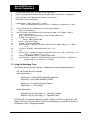
To load the ZFx86 BIOS follow this procedure:
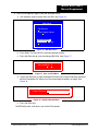
1. Start up screen containing the ZF Micro, Inc. icon.
P/N 9100-0066-01 Rev B
2
© 2001 ZF Micro Devices, Incorporated
MachZ BIOS User’s
Manual Supplement
1. Use the COPY /B command to transfer the desired BIOS image to the BIOS.ROM file.
This file must be in the same directory as amdflash.exe. For example, type:
C:\AMDFLASH> COPY /B A:zfx10400.rom BIOS.ROM
Always use the /B binary argument when you COPY from a DOS prompt.
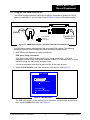
2. Set the jumpers so that the ZFx86 boots from the AMDFLASH (the board may be set
already – newer systems arrive as such). Jumper pins 4 and 6 of the FLASH CS CONF
jumper JP7, and set BOOTSTRAPS switch S3 #12 to OFF. See Figure 1.
JP7
POWER LED
IrDA
9
7
5
3
1
FRONT PANEL
FLASH CS CONF
8
6
4
2
RESET
POSTCODE D (83)
POSTCODE
Figure 1. Lower Corner of IDS Evaluation Board Jumper JP7
Since the AMDFLASH utility runs from a DOS prompt, make sure you are able to boot
using any working BIOS, or the GS from the ATMEL CHIP (if present), or a previous
version of PhoenixBIOS from the AMD Flash.
Note that if you boot DOS from the GS/ATMEL, you need to change the FLASH CS
CONF jumper JP7 from pins 3 and 5 to pins 4 and 6 (see Figure 1), and place S3 switch
#12 to the right before executing the AMDFLASH utility.
3. Boot DOS. You may boot DOS from the floppy disk or the hard disk.
4. Copy the amdflash.exe program (contained in the ZIP file) to the DOS disk. For example,
type:
C:\AMDFLASH> COPY /B A:amdflash.exe
5. Copy the .BIN files into the same directory. For example, type:
C:\AMDFLASH> COPY /B A:zfx10400rom.bin
6. Run “AMDFLASH 0".
Status messages display as the system boots.2 Do not change any jumpers unless you
boot from the ATMEL Flash (see step 2 above). This version of the program places a
copy of the BIOS.ROM in the IDS AMD flash.
2. If you have trouble running AMDFLASH 0 program, we recommend removing any ISA slot boards (except video). Currently,
AMDFLASH is “hardwired” for a 2 MB Flash Chip.
© 2001 ZF Micro Devices, Incorporated
3
P/N 9100-0066-01 Rev B
MachZ BIOS User’s
Manual Supplement
3.2. Installation Using the Dongle
Use the Z-tag Manager software application to load the BIOS image into the Z-tag Dongle.
Then use the Dongle to load the BIOS on systems that support the Z-tag interface such as
the IDS. See the examples in Chapter 4 of the ZFx86 Integrated Development System
Quick Start Guide.3
The Dongle must be loaded with a second SEEPROM. To obtain this part contact ZF
support and ask for Part Number 3100-0165-00. Dongles manufactured after January, 2001
contain this update. The Z-tag Manager provides an error message if the Dongle does not
contain enough SEEPROM.
4. BIOS Setup
To start the BIOS Setup utility, press the [F2] function key during the boot up process. The
PhoenixBIOS Setup Utility screen displays with the following selections across the top:
•
•
•
•
•
•
Main
Advanced
Security
Power
Boot
Exit
4.1. Main
The Main menu selections contain no changes with this release; therefore, that information
is not duplicated in this supplement. For information specific to the Main menu, see the
PhoenixBIOS™ 4.0 Rev6 User Manual.PDF.
4.2. Advanced
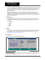
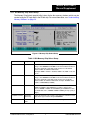
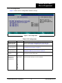
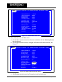
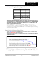
Figure 2 shows the Advanced menu selections.
Figure 2. Advanced Setup Screen
3. TheDongle’s flash programmer allows you to specify where in the flash to place the BIOS. Place the BIOS in the high
addresses of the flash. Since the ZFx86 Phoenix BIOS is a 256K image, use starting address 1C0000 if you have a 2MB Flash,
and C0000 if you have a 1 MB flash, and so on.
P/N 9100-0066-01 Rev B
4
© 2001 ZF Micro Devices, Incorporated
MachZ BIOS User’s
Manual Supplement
Table 1: Advanced Setup Screen
Feature
Options
Description
USB Host
controller
Disabled
Enabled
Enables or Disables the USB hardware. (Disabled resources are available
for other uses.) Default setting is Enabled.
USB BIOS
Legacy
Support
Disabled
Enabled
Enables or Disables support for USB Keyboard and Mouse. (Enable for
use with a non-USB aware Operating System such as DOS or UNIX.)
Default setting is Disabled.
Advanced
Chipset
Control
See ‘Advanced Chipset Control’ on page 6.
I/O Device
Configuration
See ‘I/O Device Configuration’ on page 9.
PCI
Configuration
See ‘PCI Configuration’ on page 11.
Reset
Configuration
Data
No
Yes
Select 'Yes' if you want to clear the Extended System Configuration Data
(ECSD) area. Default setting is No.
Secured Setup
Configurations
No
Yes
Yes – Prevents a Plug and Play Operating System from changing system
settings. Default setting is No.
Installed O/S
Other
Win95
Select the operating system installed on your system that you will use
most commonly. Default setting is Other.
Note: An incorrect setting causes some operating systems to display
unexpected behavior.
Large Disk
Access
Mode
Other
DOS
For UNIX, Novel NetWare, or other operating systems, select Other.
If you are installing new software and the drive fails, change this selection
and try again. Different operating systems require different
representations of drive geometries. Default setting is DOS.
Console
Redirection
Remote
Management
Baud Rate
See ‘Console Redirection’ on page 15
115.2K
57.6K
38.4K
28.8K
19.2K
14.4K
9600
2400
Selects the baud rate used for serial remote configuration mode. Default
setting is 115.2K.
© 2001 ZF Micro Devices, Incorporated
5
P/N 9100-0066-01 Rev B
MachZ BIOS User’s
Manual Supplement
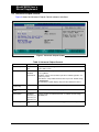
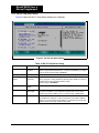
4.3. Advanced Chipset Control
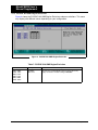
Figure 3 shows the Advanced Chipset Control submenu selections.
Figure 3. Advanced Chipset Control
Table 2: Advanced Chipset Control
Feature
Options
Description
Skip memory test
No
Yes
Skip the memory test to get a faster POST. Enable the test to create a
more stable system.
PS/2 Mouse
Disabled
Enabled
Auto Detect
Disabled – Prevents any installed PS/2 mouse from functioning, but
frees up IRQ12.
Enabled – Forces the PS/2 mouse port to be enabled regardless if a
mouse is present.
Auto Detect – Only enables the PS/2 mouse if present. Default setting
is Auto Detect.
OS Controlled – Option displays only if the OS controls the mouse.
ISA Memory Chip
Select Setup
See ‘ISA Memory Chip Select Setup’ on page 7.
ISA I/O Chip Select
Setup
See ‘ISA I/O Chip Select Setup’ on page 8.
Onboard RFD
Disabled
To mem_cs1
To mem_cs2
To mem_cs3
Selects whether the onboard flash disk is enabled. Default setting is
To mem_cs3.
Boot Through RFD
No
Yes
Select Yes to boot from the RFD as floppy A:. Default setting is No.
P/N 9100-0066-01 Rev B
6
© 2001 ZF Micro Devices, Incorporated
MachZ BIOS User’s
Manual Supplement
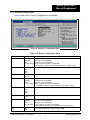
4.3.1. ISA Memory Chip Select Setup
The Memory Chip Selects provide initial values for the four memory windows which may be
created using the ZF-logic built in the ZFx86 chip. For more information, see ‘Understanding
Memory Windows’ on page 20.
Figure 4. Memory Chip Select Setup
Table 3: ISA Memory Chip Select Setup
Feature
Options
Description
Window SIZE
Enter the value for the memory window size register. Acceptable
range is from 000000H to FFF000H. Enter the hexadecimal value of
the most significant 3 HEX digits of this number. See the ZFx86
documentation for additional information.
Example: 0000H = window = disabled, 1000H = 8K, 2000 = 12K, and
so on.
Window BASE
Enter the value for the memory window base register. Acceptable
range is from 000000H to FFF000H. Enter the hexadecimal value of
the most significant 3 HEX digits of this number.See the ZFx86
documentation for additional information. Example: 0C0000 = base
address is 000C0000 (or C000:0)
Window PAGE
PAGE = 1000000 – BASE + FLASHA. If Base = 0D0000, then set
PAGE to F30000 so that D000:0 goes to address 0 in the flash.
That is 1000000 – D0000 + 0. For D0000 to go to D0000 in the flash,
set PAGE to 0, that is, 1000000 - D0000 + D0000 (you only specify 4
digits).
Read/Write Control
Read/Write
Read Only
Select the behavior of the memory range between read/write or read
only access type. Default setting is Read/Write.
Window data width
16-bits
8-bits
Select the window datapath width. Default setting is 8-bits.
© 2001 ZF Micro Devices, Incorporated
7
P/N 9100-0066-01 Rev B
MachZ BIOS User’s
Manual Supplement
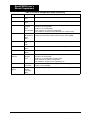
4.3.2. ISA I/O Chip Select Setup
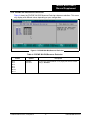
Figure 5 shows the ISA I/O Chip Select Setup menu selections.
Figure 5. ISA I/O Chip Select Setup
Table 4: ISA I/O Chip Select Setup
Feature
Options
Description
Window state
Enabled
Disabled
If the window is enabled, then I/O reads (and I/O writes if enabled) in the
address range of Base to Base+Size –1 causes the window's io_cs signal
to be asserted. Default setting is Disabled.
Base address
0 - FFFF
Enter the base address for the I/O window. Default setting is 0.
Read/Write
Control
Read/Write
Read Only
Select the behavior of the I/O range between read/write or read only
access type ports. Setting window to read only mode disables the IOW_N
signal on ISA bus for I/O window address range.
Default setting is Read/Write.
Window data width
8-bits
16-bits
Select the window datapath width. Default setting is 8-bits.
Active level
Active Low
Active High
Select the level to assert on the io_cs pin. The ZFx86 asserts the selected
level on the window's io_cs pin when the program accesses I/O in the
window range of Base to Base+Size-1. Default setting is Active Low.
Window Size
01 - 16
Select the number of consecutive I/O address to decode starting from the
I/O window base. Example, a value of 4 decodes 4 consecutive 8-bit I/O
addresses, or 2 consecutive 16-bit addresses. Decode occurs on I/O read,
and may occur on I/O write. Default setting is 01.
P/N 9100-0066-01 Rev B
8
© 2001 ZF Micro Devices, Incorporated
MachZ BIOS User’s
Manual Supplement
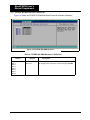
4.3.3. I/O Device Configuration
Figure 6 shows the I/O Device Configuration menu selections.
Figure 6. I/O Device Configuration Setup
Table 5: I/O Device Configuration Setup
Feature
Options
Description
Serial Port A
Disabled
Enabled
Auto
OS Controlled
Configure Serial Port A using the following options:
Disabled – No configuration
Enabled – User Configuration
Auto – BIOS or OS chooses configuration
OS Controlled – Displays when port controlled by OS. Default setting.
Base I/O address
3F8
2F8
3E8
2E8
Set the base I/O address for Serial Port A. Default setting is 3F8.
Interrupt
IRQ 3
IRQ 4
Set the interrupt for serial port A. Default setting is IRQ 4.
Serial Port B
Disabled
Enabled
Auto
OS Controlled
Configure serial port B using the following options:
Disabled – No configuration
Enabled – User Configuration
Auto – BIOS or OS chooses configuration
OS Controlled – Displayed when controlled by OS. Default setting.
Base I/O address
3F8
2F8
3E8
2E8
Set the base I/O address for Serial Port B. Default setting is 2F8.
Interrupt
IRQ 3
IRQ 4
Set the interrupt for Serial Port B. Default setting is IRQ 3.
Infrared Port
Disabled
Enabled
Auto
OS Controlled
Configure Infrared port using the following options:
Disabled – No configuration
Enabled – User Configuration
Auto – BIOS or OS chooses configuration
OS Controlled – Displays when controlled by OS. Default setting.
Mode
IrDA
FIR
Set mode for Infrared port. Default setting is IrDA.
© 2001 ZF Micro Devices, Incorporated
9
P/N 9100-0066-01 Rev B
MachZ BIOS User’s
Manual Supplement
Table 5: I/O Device Configuration Setup (Continued)
Feature
Options
Description
Base I/O address
3F8
3E8
Select the base I/O address for Infrared port. Default setting is 3E8.
Interrupt
IRQ 3
IRQ 5
Select the interrupt for the Infrared port. Default setting is IRQ 5.
Parallel port
Disabled
Enabled
Auto
OS Controlled
Configure parallel port using options:
Disabled – No configuration
Enabled – User Configuration
Auto – BIOS or OS selects the configuration
OS Controlled – Displayed when controlled by OS. Default setting.
Mode
Output only
Bi-directional
EPP
ECP
Set the mode for the parallel port using the following options:
Output only, Bi-directional, EPP, and ECP. Default setting is ECP.
Base I/O address
378
278
3BC
Set the base I/O address for the parallel port. Default setting is 387.
Interrupt
IRQ 5
IRQ 7
Set the interrupt for the parallel port. Default setting is IRQ 7.
DMA channel
DMA 1
DMA 3
Set the DMA channel for the parallel port. Default setting is DMA 1.
Floppy disk
controller
Disabled
Enabled
Auto
Configure using the following options:
Disabled – No configuration
Enabled – User Configuration. Default setting.
Auto – BIOS or OS chooses configuration
OS Controlled – Displayed when controlled by OS.
Base I/O address
Primary
Secondary
Set the base I/O address for the floppy disk controller using options.
Default setting is Primary.
Local Bus IDE
adapter
Disabled
Primary
Secondary
Both
Enable the integrated local bus IDE adapter. Default setting is Both.
P/N 9100-0066-01 Rev B
10
© 2001 ZF Micro Devices, Incorporated
MachZ BIOS User’s
Manual Supplement
4.3.4. PCI Configuration
Figure 7 shows the PCI Configuration submenu settings.
Figure 7. PCI Configuration
Table 6: PCI Configuration
Feature
Options
Description
PCI/PNP ISA UMB
Region Exclusion
Reserve specific upper memory blocks for use by legacy ISA
devices. See ‘PCI/PNP ISA UMB Region Exclusion’ on page 12.
PCI/PNP ISA IRQ
Resource Exclusion
Reserve specific IRQ's for use by legacy ISA devices. See ‘PCI/PNP
ISA IRQ Resource Exclusion’ on page 13.
PCI/PNP ISA DMA
Resource Exclusion
Reserve specific DMA channels for use by legacy ISA devices. See
‘PCI/PNP ISA DMA Resource Exclusion’ on page 14.
ISA graphics device
installed:
No
Yes
Enable ISA (non-VGA) graphics device to access palette data in PCI
VGA device. Default setting is No.
PCI IRQ line 1
PCI IRQ line 2
PCI IRQ line 3
PCI IRQ line 4
Disabled
Auto Select
3
4
5
7
9
10
11
12
14
15
PCI devices use hardware interrupts called IRQ's. A PCI device
cannot use IRQ's already in use by ISA Enable.
© 2001 ZF Micro Devices, Incorporated
11
P/N 9100-0066-01 Rev B
MachZ BIOS User’s
Manual Supplement
4.3.5. PCI/PNP ISA UMB Region Exclusion
Figure 8 shows the PCI/PNP ISA UMB Region Exclusion submenu selections. This menu
may display with different values depending on your configuration .
Figure 8. PCI/PNP ISA UMB Region Exclusion
Table 7: PCI/PNP ISA UMB Region Exclusion
Feature
C800 - CBFF
CC00 - CFFF
D000 - D3FF
D400 - D7FF
D800 - DBFF
DC00 - DFFF
P/N 9100-0066-01 Rev B
Options
Available
Reserved
Description
Reserves the specified block of upper memory for use by
legacy ISA devices. Default setting is Available.
12
© 2001 ZF Micro Devices, Incorporated
MachZ BIOS User’s
Manual Supplement
4.3.6. PCI/PNP ISA IRQ Resource Exclusion
Figure 9 shows the PCI/PNP ISA IRQ Resource Exclusion submenu selections. This menu
may display with different values depending on your configuration.
Figure 9. PCI/PNP ISA IRQ Resource Exclusion
Table 8: PCI/PNP ISA IRQ Resource Exclusion
Feature
IRQ 3
IRQ 4
IRQ 5
IRQ 7
IRQ 9
IRQ 10
IRQ 11
Options
Available
Reserved
© 2001 ZF Micro Devices, Incorporated
Description
Reserves the specified IRQ for use by legacy ISA devices. Default
setting is Available.
13
P/N 9100-0066-01 Rev B
MachZ BIOS User’s
Manual Supplement
4.3.7. PCI/PNP ISA DMA Resource Exclusion
Figure 10 shows the PCI/PNP ISA DMA Resource Exclusion submenu selections.
Figure 10. PCI/PNP ISA DMA Resource
Table 9: PCI/PNP ISA DMA Resources Exclusion
Feature
DMA 0
DMA 1
DMA 2
DMA 3
DMA 4
DMA 5
DMA 6
DMA 7
P/N 9100-0066-01 Rev B
Options
Available
Reserved
Description
Reserves the specified DMA channel for use by
non-Plug-and-Play ISA devices. Default setting is Available.
14
© 2001 ZF Micro Devices, Incorporated
MachZ BIOS User’s
Manual Supplement
4.3.8. Console Redirection
UCR (Universal Console Redirect) feature supports those embedded systems which do not
use a keyboard or monitor. The BIOS Binary Image file may be configured for this feature
using the ZEB utility. See “Using the ZEB Editor with the IDS” on page 17.
A null modem cable connection is required between the ZFx86 COM A (COM1) and a PC/
ANSI terminal or terminal emulator such as Procomm™ or Hyperterminal™. Text mode
video operations are only supported during console redirect.
Figure 11. Console Redirection
Table 10: Console Redirection
Feature
Options
Description
Com Port Address
Disabled
On-board COM A
On-board COM B
If enabled, ZFx86 uses a port on the motherboard. Default setting is
Disabled. (Console redirection default is COM A.)
Baud Rate
300
1200
2400
9600
19.2 K
38.4 K
57.6 K
115.2 K
Enables the specified baud rate. Default setting is 19.2K. (Console
redirection default is 19.2K.)
Console Type
PC ANSI
VT100
Enables the specified console type. Default setting is PC ANSI.
Flow Control
None
XON/XOFF
CTS/RTS
Enables Flow Control. Default setting is CTS/RTS.
Console connection
Direct
Via modem
Indicates whether the console is connected directly to the system or a
modem. Default setting is Direct.
Continue C.R. after
POST
Off
On
Enables Console Redirection after OS loads. Default setting is Off.
(Console redirection default is On.)
© 2001 ZF Micro Devices, Incorporated
15
P/N 9100-0066-01 Rev B
MachZ BIOS User’s
Manual Supplement
4.4. Other Setup Screens
For information on the screens below, refer to PhoenixBIOS™ 4.0 Rev6 User Manual.PDF
which is supplied on the ZF CD ROM.
•
•
•
•
•
Security
Power
Boot
Exit
Help
5. ZFlash OS LOADER
This feature allows Operating Systems, such as Linux or VxWorks to load and boot from the
same flash device that holds the BIOS.
Prior to a boot attempt of standard media devices, the ZFx86 BIOS scans external Flash
devices address blocks. These blocks are defined by the user configurable Memory
Window Chip Selects and contain a standard legacy ISA extension ROM header. A
checksum (modulo 100h) is performed, and if successful, the BIOS transfers the boot
attempt to code beginning at byte 3 of the special header. When the transfer is executed, a
signature parameter value of 'MORX' is passed in register EDX, allowing the user to
authenticate the call.
Thus, user supplied external code may be installed in flash and can continue the boot
function using its own algorithms. Details are available from ZF Micro Devices. Ask support
for the “Booting User Software From Flash Chips” Software Note, Part # 9100-0067-00 or
download this document from the ZF Micro Devices website: http://www.zfmicro.com
6. Using the ZF Edit BIOS (ZEB) Utility
The ZF Edit BIOS utility, ZEB.EXE, allows you to establish custom default BIOS settings.
The editor is ideal for those ZFx86 embedded systems with no battery backed CMOS
storage, and allows additional debug flexibility when you bring up new designs. ZEB runs in
either DOS or Windows.
Remember to disable your CMOS battery (if your system contains one) and to completely
re-power the system each time you experiment with BIOS changes. The power reset
guarantees that the BIOS reboot launches with the new defaults you selected.
This utility supports creating a debug version of the BIOS that outputs POST Codes on the
serial port. See the ZEB Debug menu item.
P/N 9100-0066-01 Rev B
16
© 2001 ZF Micro Devices, Incorporated
MachZ BIOS User’s
Manual Supplement
6.1. Using the ZEB Editor with the IDS
Use ZEB to change the default CMOS BIOS settings. Remember to disable the CMOS
battery by setting pins 2 and 3 to Clear. Refer to Figure 12 for the JP5 jumper location.
BAT1
PC SPEAKER
Battery
COM2
JP5
CMOS BATTERY
1–2 NORM
2–3 CLR CMOS
PARALLEL PORT
COM1
Parallel Port
Connector
Figure 12. CMOS Battery Jumper JP5 (Part of the IDS Evaluation Board)
The ZEB menus contain information on how to change BIOS settings. The following
procedure illustrates how to change the default Summary Window setting.
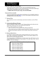
1. Start ZEB at a DOS prompt by typing the following:
ZEB <your_image_name.rom>
If you do not enter a BIOS Image name (<your_image_name.rom>), a listing of
directories and files found in the launch directory displays. Use the arrow keys to select
the BIOS Image you want to edit, and press Enter.
Use the up and down arrow keys to select an item on the start up menu.
2. Select the Edit Defaults menu item, and press the Enter key. See Figure 13.
Main Menu
Edit Defaults
Load Original Values
Save and Exit
Quit Without Saving
Figure 13. ZEB Main Menu
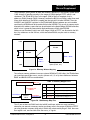
The ZEB utility displays seven top-level menu selections. Using the right and left arrow
keys, select the Main menu item. See Figure 14.
© 2001 ZF Micro Devices, Incorporated
17
P/N 9100-0066-01 Rev B
MachZ BIOS User’s
Manual Supplement
Main
Advanced
IO Devices
PCI
Memory Windows IO Windows Debug
Legacy Diskette A:
Legacy Diskette B:
Primary Master
Primary Slave
Secondary Master
Secondary Slave
Boot Drive Order
Boot through RFD
1.44 mb
NONE
AUTO
AUTO
AUTO
AUTO
Floppy Disk
No
Memory Cache:
Summary Screen:
Floppy check:
Hand Disk Pre-delay:
NumLock
Key Click:
Enabled
Disabled
Disabled
Disabled
Off
Disabled
Figure 14. ZEB Main Menu Selections
3. Press Enter to access the Main menu.
a. Use the down arrow to move down the menu selections until the Summary Screen
item is selected.
b. Use the right and left arrow keys to toggle the Enabled or Disabled selection. See
Figure 15.
Main
Advanced
IO Devices PCI
Memory Windows IO Windows
Legacy Diskette A:
Legacy Diskette B:
Primary Master
Primary Slave
Secondary Master
Secondary Slave
Boot Drive Order
Boot through RFD
1.44 mb
NONE
AUTO
AUTO
AUTO
AUTO
Floppy Disk
No
Memory Cache:
Summary Screen:
Floppy check:
Hand Disk Pre-delay:
NumLock
Key Click:
Enabled
Enabled
Disabled
Disabled
Off
Disabled
Debug
Figure 15. Summary Screen Enable Setting
c. With Enabled selected, press the Escape key to exit the Main menu.
P/N 9100-0066-01 Rev B
18
© 2001 ZF Micro Devices, Incorporated
MachZ BIOS User’s
Manual Supplement
4. Press the Escape key again to exit the ZEB Main menu.
a. Use the down arrow to select Save and Exit. See Figure 16.
Main Menu
Edit Defaults
Load Original Values
Save and Exit
Quit Without Saving
Figure 16. ZEB Main Menu
b. Press Enter. The Save & Exit? command prompt displays.
c. Press the Enter key to save the changed BIOS file. See Figure 17.
Save and Exit? Y
Figure 17. Save and Exit Menu
d. Type a new file name, or type the original file name in the Output Filename: prompt as
desired. Remember, file names may not exceed eight characters in length. See
Figure 18.
Output Filename:
Figure 18. Output Filename Menu
e. Press the Enter key.
The ZEB utility exits, and returns you to the DOS prompt.
© 2001 ZF Micro Devices, Incorporated
19
P/N 9100-0066-01 Rev B
MachZ BIOS User’s
Manual Supplement
Copy <your_image.rom> to BIOS.ROM file
To verify that your BIOS changes are correct, copy your edited BIOS image to the
AMDFLASH directory using the “/b” binary switch. Remember to rename your edited image
to BIOS.ROM using the following copy command, for example:
C:\AMDFLASH> COPY /B <your_image_name.rom> BIOS.ROM
Remove AC-Power to the IDS
The IDS non-volatile RAM is battery backed, and although you have disabled the battery by
jumpering JP5 pins 2 and 3 (see Figure 12), you must also re-power the IDS board to erase
the original data in the non-volatile RAM.
7. Technical Tips
This section discusses items and techniques particular to the effective use of the ZFx86
BIOS.
7.1. Understanding Memory Windows
Memory windows are a feature of the ZF Logic. Memory windows provide chip select and
addressing for SRAM and Flash Chips external to the ZFx86 chip.
Memory windows benefit the user two ways:
•
•
Allows interconnect to Flash and SRAM chips without extra glue logic
Allows addressing of up to 64 MB of external Flash/SRAM (4 chip selects times 16 MB
per chip select) through an aperture in the ISA address space called a memory window.
7.1.1. Memory Window Basics
XT computers contained a paged memory scheme that allows the XT to access memory
above 1 MB. A small aperture (window) below 1 MB was used to address perhaps 1 to 8
MB of additional RAM through page switching.
The memory windows on the ZFx86 work in a similar manner. From a DOS prompt, run the
program AMDFLASH on the ZFx86 and specify option P in the Main Menu screen. You see
a printout similar to the following:
Phoenix Mach Z BIOS Memory Window Setup Calculator
Window OK at C8000–CBFFFH
Window OK at CC000–CFFFFH
Window OK at D0000–D3FFFH
Window OK at D4000–D7FFFH
Window OK at D8000–DBFFFH
Window OK at DC000–DFFFFH
P/N 9100-0066-01 Rev B
20
© 2001 ZF Micro Devices, Incorporated
MachZ BIOS User’s
Manual Supplement
These numbers specify where to place the windows (apertures) in the memory space below
1 MB. Actually, it specifies memory in the range of C0000 through FFFFF which is not
shadowed. The ZFx86 BIOS lives in the upper 128K of the first megabyte, that is,
addresses E0000 through F0000. However, to allow the BIOS to run faster, rather than read
it from 8-bit wide flash, the BIOS is copied into the typical 32-bit wide SDRAM. Then the
SHADRC and SHADWC registers in the ZFx86 North Bridge hardware are set to enable
read from the SDRAM and not to enable Write to the SDRAM. This results in memory reads
directed to this address space that are also directed to the North Bridge SDRAM controller,
which in turn is generally connected to high performance 32-bit wide SDRAM.
Addresses not shadowed, which are in the range C0000 to FFFFF, are directed to the ISA
bus. Any addresses on the ISA bus, which are below E0000, may be used as memory
windows.
16 MB
Window
SIZE
Window
PAGE + BASE
BASE
Address
0
External Address
Space (Flash, etc.)
0 MB
ISA Address Space
Figure 19. Memory Window Mapping
To use these memory windows to access external SRAM or FLASH chips, the ZFx86 allows
you to activate one of four mem_csn pins (where n=0,1,2, or 3) when addresses between
BASE and BASE+SIZE are encountered.
ISA Memory Mapper
Translated ISA
Address
ISA Address
Address
MUX
Table 11: Memory Mapper Pins
Mem_cs*
ISA Address
ISA Address
Pin
Name*
Description
B04
Mem_cs0
ZF Logic Memory Mapper CS 0
D05
Mem_cs1
ZF Logic Memory Mapper CS 1
A03
Mem_cs2
ZF Logic Memory Mapper CS 2
C04
Mem_cs3
ZF Logic Memory Mapper CS 3
Figure 20. ISA Memory Map Pins
Thus if you set base to D0000 and size to 64K (and those addresses were available),
whenever you execute a memory read or a memory write in the range of D0000 to DFFFF
you also generate a memory chip select. Which chip select would you get? Well, there are
four register sets, one for each of the four mem_cs signals.
© 2001 ZF Micro Devices, Incorporated
21
P/N 9100-0066-01 Rev B
MachZ BIOS User’s
Manual Supplement
The address which comes out on the ISA bus is translated by the memory window
hardware. In general, the question is this: how do I move the target window through my
flash chip so that using the fixed window I have set up in the ZFx86 address space I can
reference all of the data in the flash chip (up to 16 MB). This answer is embodied in a
formula for setting the value of the PAGE register:
PAGE = 1000000 – BASE + FLASHA.
If BASE = 0D0000 then set PAGE to F30000 so that D000:0 goes to address 0 in the Flash.
That is 1000000 – D0000 + 0.
For D0000 to go to D0000 in the flash, set PAGE to 0. That is, 1000000 – D0000 + D0000.
(only specify 6 digits).
7.1.2. Using the BIOS to Set Initial Memory Window Positions
AMDFLASH contains a calculator to make the initial setup of your windows easier. Set the
initial values of the BASE/SIZE/PAGE registers using exactly the same technique you use
in your own software to reset or move these memory windows.
The operative part of the BASE/SIZE/PAGE registers is a 12 bit field (3 hex digits) out of a
32-bit register. The BASE/SIZE/PAGE registers are 32-bits wide, but only bits 23–12 are
used (12 bits or 3 hex digits). The possible ranges of data written to these registers is thus
000000H – FFF000H.
Bits 23–16
Bits 15–12
12 bits
8 bits
12 bits
24|23
31
00H
12|11
0
00H
User Defined
32 bits
Figure 20. Fields in 32-bit memory settings register
Since each field is 12 bits wide, the actual data values are 000 to FFF hex (in the 12 bit
field).
If you want the window to start at D0000 in the ZFx86 address space, set the BASE to
0D0000 hex, that is, 0D0 in the 12-bit field and in the BIOS settings for the Memory Window
BASE.
P/N 9100-0066-01 Rev B
22
© 2001 ZF Micro Devices, Incorporated
MachZ BIOS User’s
Manual Supplement
Table 12 shows the values used to setup a Memory Window Chip Select that enables
blocks placed at flash address 0 to be mapped to ISA addresses shown in the first column.
Table 12: Sample Window Calculations
ISA Window Base
BASE (hex)
PAGE (hex)
C8000
C8
F38
CC000
CC
F34
D0000
D0
F30
D4000
D4
F26
D8000
D8
F28
DC000
DC
F24
Calculate the window SIZE as BASE to BASE+SIZE where it is assumed that the right most
12 bits are implicitly FFF. Therefore, a size of 001000 hex would be 1FFF, thereby providing
an 8K window. Note that you might think that 0 would provide a 4K window; however, we
decode 0 internally to disable the window.
Treat the PAGE field as a signed number (if PAGE = –BASE then the target is the
beginning of the flash), but because all 32 bits are not available, it becomes a bit tricky.
It is best to use the calculator built into AMDFLASH. An example of the printout and a copy
of the source code in C follows.
Sample Code for Initial Memory Window Positions
Create a 32K window starting at D0000 in the ZFx86 address space. The window initially
points to an offset 2000H within the flash chip.
Example: Set the Page register to 00F32000H (or F32 in the ZFx86 Phoenix BIOS Memory
Window Setup screen).
.
Phoenix ZFx86 BIOS Memory Window Setup Calculator
Helper: Enter Window Size between 8K and 16384K: 32
Recommended Value for Size = 007000H
Enter Desired Window Base in Hex (example DC000) D0000
Enter Desired Window Size in Hex (example 1000 = 8K, FFF000 = 16 MB 7000
Enter Flash Target Address in Hex (example 2000 = 8K) 2000
NOTE:In the following example, the program creates a 32K window starting at D0000H which
points initially to offset 2000H in the flash using BASE = 0D0H, SIZE = 007H, and
PAGE = F32H.
© 2001 ZF Micro Devices, Incorporated
23
P/N 9100-0066-01 Rev B
MachZ BIOS User’s
Manual Supplement
1
2
3
4
5
6
7
8
9
10
11
12
13
14
15
16
17
18
19
20
21
22
23
24
25
unsigned long ulBase, ulSize, ulTarget, ulPage, ulDesiredK;
printf ("\r\n\n\nPhoenix ZFx86 BIOS Memory Window Setup Calculator \r\n", uiWorkingCS);
printf ("\r\nHelper: Enter Window Size between 8 and 16384K: ");
ulDesiredK = uiScanInDecimal(0);
if ((ulDesiredK >= 8) && (ulDesiredK <= 16384))
printf ("\r\n Recommended Value for ""Size"" = %06lXH\r\n", (ulDesiredK-4) * 1024 );
printf ("\r\nEnter Desired Window Base in Hex (example DC000) ");
ulBase = ulScanInHex ();
printf ("\r\nEnter Desired Window Size in Hex (example 1000 = 8K, FFF000 = 16 MB ");
ulSize = ulScanInHex ();
printf ("\r\nEnter Flash Target Address in Hex (example 2000 = 8K) ");
ulTarget = ulScanInHex ();
ulBase = ulBase & 0xFFF000;
ulSize = ulSize & 0xFFF000 ;
ulTarget = ulTarget & 0xFFF000;
printf ("\r\nBase = %08lXH or %03lXH or %04ld decimal", ulBase, ulBase >> 12, ulBase
>>12);
if (ulSize == 0) printf ("\r\nWindow Disabled Size == 0");
else
printf ("\r\nSize = %08lXH or %03lXH or %04ld decimal for Size = %dK", ulSize, ulSize >> 12,
ulSize >>12, ((ulSize >> 12) + 1) * 4);
ulPage = (0x1000000 - ulBase + ulTarget) & 0xFFF000;
printf ("\r\nPage = %08lXH or %03lXH or %04ld decimal for Flash Offset = %08lXH\r\n\n",
ulPage, ulPage >> 12, ulPage >>12, ulTarget);
7.2. Using the Watchdog TImer
The ZFx86's Watch Dog Timer function is implemented using the following interface:
INT 15H System Services Interrupt
Calling Parameters:
Register AH = C3H Enable/Disable Watchdog Timer
Register AL = 00 Disable Watchdog Timeout
Register AL = 01 Enable Watchdog Timeout
Register BX = 1 - 255 seconds
Return Parameters:
Register Flag CF (Carry Flag) = 0 = Operation Complete
Register Flag CF (Carry Flag) = 1 = Operation Failed
WDTON.EXE is a sample test program for WDT functions. WDTON.c is the source code
written in MS C and may be used as a tutorial for developing user based WDT routines in
Assembler or Other C language compilers.
P/N 9100-0066-01 Rev B
24
© 2001 ZF Micro Devices, Incorporated
MachZ BIOS User’s
Manual Supplement
As an example, set the IDS board's watchdog Jumper J2 to short pin 2 to 3. (WD OSC INT).
Then, at a DOS prompt, run WDTON 10. The WDTON utility displays the time continuously
for 10 seconds. The test keeps the ZFx86's watchdog timer from firing until the ten second
interval. At that time the watchdog timer fires and the system resets.
WDTON.C Sample Program
6 // Tests WDT INT 15 Functions
7
8 #include <ctype.h>
9 #include <io.h>
10 #include <dos.h>
11 #include <stdlib.h>
12 #include <stdio.h>
13 #include <string.h>
14 #include <time.h>
15
16 void main(argc,argv)
17 int argc;
18 char *argv[];
19 {
20 char tbuffer[9];
21 union REGS inregs, outregs;
22 int delay_value=0;
23 int wait_value=0;
24 int start_secs = 0;
25 int stop_secs = 0;
26 time_t t1,t2;
27
28 setbuf(stdout,NULL);
29
30 if(argc !=2)
// only two args allowed
31
{ printf(“\nError: \n");
32
printf("Format: WDTON <secs> i.e WDTON 10"); exit(EXIT_FAILURE);}
33
34 delay_value = (abs(atoi(argv[1])));
35 wait_value = delay_value*2;
36 system("cls");
37 //_strtime (tbuffer);
38 printf("\nWatch Dog Timer Tickle Test\n");
39 printf("\nSystem will REBOOT in %2.2d seconds",delay_value);
40 printf("\nStart Time %s\n", _strtime (tbuffer));
41
42 //start_secs = (atoi(&tbuffer[6]));
43 start_secs = (time(&t1));
44 //printf("Startsecs == %d\n", start_secs);
45 //stop_secs =+ (atoi(&tbuffer[6]));
46 //printf("Start Secs %d\n", start_secs);
47
48 time(&t1);
49
50 while ((difftime(t2,t1) != delay_value+1))
51
{
© 2001 ZF Micro Devices, Incorporated
25
P/N 9100-0066-01 Rev B
MachZ BIOS User’s
Manual Supplement
52
53
54
55
56
57
58
59
60
61
62
63
64
65
66
printf("Tickling WDT %s\r", _strtime (tbuffer));
time(&t2);
}
printf("WDT FAILED %s\n", _strtime (tbuffer));
printf("\n");
while ((difftime(t2,t1) < delay_value+7))
{
printf("Waiting 5 more seconds: %s\r", _strtime (tbuffer));
time(&t2);
}
outregs.x.ax = 0xc301;
outregs.x.bx = delay_value;
int86(0x15 ,&inregs, &outregs);
printf("\nINT 15 function C3 01 failed CF = %d\n", outregs.x.cflag);
}
P/N 9100-0066-01 Rev B
26
© 2001 ZF Micro Devices, Incorporated
MachZ BIOS User’s
Manual Supplement
ZF Micro Devices, Inc.
1052 Elwell Court
Palo Alto, California 94303
(650) 965-3800 · Fax 965-4050
www.zfmicro.com
© 2001 ZF Micro Devices, Incorporated
27
P/N 9100-0066-01 Rev B