1
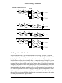
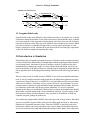
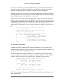
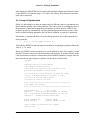
High Speed CMOS VLSI Design
Lecture 3: Sizing & Simulation
(c) 1997 David Harris
1.0 Sizing with Side loads
We have learned to size simple paths consisting of a cascade of gates in which each gate
drives only the next. In most interesting paths, gates also drive other gates leading into
other paths. Gates may also drive fixed sources of capacitance, such as long wires. Sizing
such gates becomes a more difficult problem and often does not have a closed form solution. In this section, we will explore some of the issues and describe techniques and heuristics for sizing paths with side loads.
1.1 Types of Side Loads
We can divide side loads into various categories. Ratio side loads contribute capacitance
proportional to that of the main path being sized. Two subcategories of ratio side loads are
identical side loads and proportional side loads. Identical side loads are paths topologically identical to the main path that must drive identical loads in equal time. A classic
example is an address decoder. One address line drives many bits of the decoder. Each bit
involves identical gates and should complete at the same time. Proportional side loads are
paths that are similar but not identical, yet must still drive identical loads in the same or
less time than the critical path. For example, a carry lookahead circuit in an adder must
compute all the carries into a block of N bits. The most significant bit requires the most
complex logic and therefore is most critical. The other bits involve similar logic and
should complete no later than the most significant bit, so are called proportional side
loads. Fixed side loads are loads such as wires or gates in other paths that have already
been sized and cannot be changed. Finally, irregular side loads are loads that are unknown,
have some arbitrary timing relationship with the path being sized, and are sufficiently
complex that dividing capacitance between the primary path and the side load may be nontrivial.
Figure 1 illustrates several these types of side loads. Let the main path being sized be AB.
Suppose AC, AD, and AE all are equally critical. AC is an identical side load; I4 and I8 in
the portion XC are identical to I5 and I9 in XB and are equally critical. AD is a proportional side load. The path is nearly identical, but the NAND2 gate has lower logical effort
than a NAND3 gate and can therefore be sized smaller than a NAND3 while achieving
equal delay. AE involves an irregular side load; the path through the NOR is difficult to
compare with a two stage path through a NAND and an inverter. If the fanout from X to E
is large, the NOR gate might have to be sized much larger than the NAND gates to drive
November 4, 1997
1 / 16
Lecture 3: Sizing & Simulation
the load in a reasonable amount of time. If the fanout is small, the NOR might be sized
comparably to the NANDs. The path AF has wire, representing a fixed load. The inverter
driving the wire may see a load dominated by the wire, almost independent of the final
inverter size if the final inverter is not huge. The path is also irregular, because it is difficult
to decide how inverters I1 and I2 should be ratioed without information on the criticality
and delay of paths WB and WF. Finally, the path AG goes through non-critical logic.
Therefore, inverter I3 may be sized at minimum size to buffer the non-critical portion of
the circuit and minimize its load on the critical path. Thus, inverter I3 shows up as a fixed
side load.
FIGURE 1. Types of Side loads
A
I0
W
I1
X
I4
I8
AB: Main Path
B
C1
Side Loads:
I5
I9
C
C1
I6
I10
D
AC: Identical
AD: Proportional
C1
E
I7
I2
2 mm wire
I3
I11
Noncritical Logic
F
G
AE: Irregular
C1
C2 AF: Fixed &
Irregular
AG: Fixed
1.2 Identical Side Loads
Identical side loads are easy to deal with. Each contributes the same capacitance as the
main path. Therefore, a path with N-1 identical side loads can be sized as a single main
path with a logical effort N times larger. Then, the sizes of the original path are computed.
For example, the circuit in Figure 2 has an identical side load shown in part I. In part II, it
is lumped into a single path with twice the logical effort where the side load split off. The
total gain of the path is the total fanout times the total logical effort: (24/1)*1*10/3*1*1 =
80. Thus, the gain per stage is about the fourth root of 80, or 3. In part III, the equivalent
circuit is sized with a gain of about 3 per stage. In part IV, the original path is restored,
where the 10 units of capacitance on the combined gate is divided into 5 units on each
branch.
November 4, 1997
2 / 16
Lecture 3: Sizing & Simulation
FIGURE 2. Identical Side Load
I: Path
A
W
I0
LE: 1
Cin: 1
X
I1
I4
LE: 1
Cin:
B
I8
LE: 5/3
Cin:
I5
C1=24
LE: 1
Cin:
C
I9
LE: 5/3
Cin:
C1=24
LE: 1
Cin:
II: Equivalent Circuit
A
W
I0
I1
LE: 1
Cin: 1
X
I4
LE: 1
Cin:
B
I8
LE: 10/3
Cin:
C1=24
LE: 1
Cin:
III: Sized Equivalent Circuit
A
W
I0
I1
LE: 1
Cin: 1
A
I0
W
LE: 1
Cin: 1
LE: 1
Cin: 3
I1
LE: 1
Cin: 3
X
I4
B
I8
C1=24
LE: 10/3 LE: 1
Cin: 10
Cin: 8
IV: Sized Original Path
X
I4
LE: 5/3
Cin: 5
I5
B
I8
C1=24
LE: 1
Cin: 8
C
I9
LE: 5/3
Cin: 5
LE: 1
Cin: 8
C1=24
1.3 Proportional Side Loads
Proportional side loads are not too difficult either. For example, in Figure 3, one path
involves I4, a 3-input NAND gate, while the other involves I5, a 2-input NAND gate. If
both paths have the same time to complete, I5 can be smaller than I4 because it has lower
logical effort as well as a lower intrinsic delay. A conservative way of sizing I5 to guarantee it is no slower than I4 is to give it the same gain as I4. Thus, the fanout-dependent component of the two delays will be equal and the intrinsic delay of I5 will be lower, making
I5 slightly faster than I4. This is easier than trying to exactly match the delays of the gates,
which would allow I5 to be even smaller but would require more detailed and accurate
information about the intrinsic gate delays. To give each proportional gate equal gain, we
can create an equivalent circuit with a single gate having logical effort equal to the sum of
all the logical efforts on the proportional branches. In this case, 5/3 + 4/3 = 9/3. Then size
the equivalent circuit path and finally distribute the capacitance across gates in the original
circuit in proportion to their logical efforts.
November 4, 1997
3 / 16
Lecture 3: Sizing & Simulation
FIGURE 3. Proportional Side Load
I: Path
A
W
I0
LE: 1
Cin: 1
X
I1
I4
LE: 1
Cin:
B
I8
LE: 5/3
Cin:
I5
C1=24
LE: 1
Cin:
C
I9
LE: 4/3
Cin:
C1=24
LE: 1
Cin:
II: Equivalent Circuit
A
W
I0
I1
LE: 1
Cin: 1
X
I4
LE: 1
Cin:
B
I8
LE: 9/3
Cin:
C1=24
LE: 1
Cin:
III: Sized Equivalent Circuit
A
W
I0
I1
LE: 1
Cin: 1
A
I0
W
LE: 1
Cin: 1
LE: 1
Cin: 3
I1
LE: 1
Cin: 3
X
I4
B
I8
C1=24
LE:9/3
LE: 1
Cin: 9
Cin: 8
IV: Sized Original Path
X
I4
LE: 5/3
Cin: 5
I5
B
I8
C1=24
LE: 1
Cin: 8
C
I9
LE: 4/3
Cin: 4
LE: 1
Cin: 8
C1=24
1.4 Fixed Side Loads
Fixed side loads are tricky because they may result in different gains per stage before and
after the fixed side load. For example, consider the circuit in Figure 4 which includes a
wire having capacitance equal to 150 times that of a unit sized gate. Note how the Cin of
the first gate in this design is 3, not 1, for a change. As long as I11 has significantly less
capacitance than the wire, it will not change the delay of I2 very much. Therefore, it can
be made quite large to quickly drive the 30 unit load unless area restrictions require trading some performance for lower area. A reasonable choice could be to size I11 at 30 so it
has a gain of 1; bringing the gain even lower barely improves speed. Now, I2 drives a load
equal to 150 + 30 = 180. Thus, the total gain through I0 and I2 is the total fanout times the
total logical effort, (180/3) * 1 * 1 = 60. Thus, the gain per stage is about 8, and sizing I2 at
24 is about right.
November 4, 1997
4 / 16
Lecture 3: Sizing & Simulation
FIGURE 4. Fixed Side Load
A
I: Original Circuit
I2
I0
LE: 1
Cin: 3
LE: 1 Cwire = 150
Cin:
I11
F
I11
F
LE: 1
Cin:
C=30
II: Sized Circuit
A
I2
I0
LE: 1
Cin: 3
LE: 1
Cin: 24
Cwire = 150
LE: 1
Cin: 30
C=30
1.5 Irregular Side Loads
Irregular loads are the most difficult to deal with because there is no simple way to divide
capacitance among the branches. If one path is much more critical than the other, it should
receive the majority of the capacitance on the branch; in the limit when one side is entirely
non-critical, the non-critical side can just be buffered with a minimum size inverter. When
criticality is similar, a reasonable first approach is to assign equal capacitance to each
branch, complete the sizing, simulate the result, then iterate by increasing the capacitance
on the side with less margin and repeating the sizing.
2.0 Introduction to Simulation
Fabricating a chip is a lengthy and expensive process. Designers need to estimate the delay
of circuits and test the functionality of unusual ideas without repeating the fabrication process too many times. Simulation is the art of building a model of a physical chip, then
mathematically evaluating the model. It is much cheaper than fabrication, but is only as
good as the quality of the model. Moreover, learning what is important to model and what
can be ignored can be challenging and evaluating a detailed model takes large amounts of
time.
There are many levels of model accuracy. HSPICE is one of the most detailed simulation
tools; it can use complex transistor models and solve the differential equations to predict
currents and voltages. However, even HSPICE is very limited because the user must know
what cases to simulate. Transistors vary by at least a factor of 2 in performance over processing extremes; therefore a single simulation cannot possibly match all chips. Moreover,
two transistors on the same chip do not perform identically. If a circuit’s operation
depends on the degree to which ideally identical devices match, the designer must identify
the possible mismatch and include it in the simulation. Similarly, if power supply or thermal variations impact circuit performance, they may have to be modeled. As with any
computer program, garbage in-garbage out.
Even with fairly simple models, HSPICE takes too long to run on large circuits. Individual
gates are acceptable; larger modules such as 64 bit adders push the limits of what can be
simulated in a reasonable amount of time. Therefore, HSPICE is generally reserved to
characterize a library and verify potentially risky circuits. Other less detailed simulators
are used to verify the entire chip and estimate the timing of all the paths. These other tools,
November 4, 1997
5 / 16
Lecture 3: Sizing & Simulation
such as static timing analyzers, base timing information upon simpler models curve fit to
data from a modest number of SPICE simulations.
3.0 Using HSPICE
This section gives a brief example of using HSPICE. If you have never used the simulator,
you will probably want a more detailed tutorial. For instance, a tutorial and lengthy reference manual are available at:
http://yake.ecn.purdue.edu/~seib/ee255/spicehandouts.html
Those who like a hard copy of a reference manual may prefer the 3-volume HSPICE
User’s Manual. Volume I is especially handy for power users who want to take advantage
of advanced measurement and optimization commands.
The following code is an example of a SPICE deck which measures the delay through an
inverter. The first line should always be a comment because it is ignored by SPICE.
* example.hsp
*
+
*
*
Written 9/13/97 by David Harris
[email protected]
This spice deck measures the delay of an
inverter with a sharp ramp input.
**************************************
* Set supply and library
**************************************
.param Supply=2.5* Set voltage
.protect
* Don’t print the contents of library
.lib ‘~/lib/cad/spice/hp0.6u/opConditions.lib’ TT
* Load the library
.unprotect * Resume printing SPICE deck
.opt scale=0.35u* Define lambda
* (half minimum channel length)
**************************************
* Define power supply
**************************************
.global Vdd Gnd
Vdd
Vdd
Gnd
‘Supply’
**************************************
* Define Subcircuits
**************************************
.subckt inv In Out N=8 P=16
* Assumes 5 lambda of diffusion on the source/drain
m1
Out In Gnd Gnd nmos l=2 w=N
November 4, 1997
6 / 16
Lecture 3: Sizing & Simulation
+
as=’5*N’ ad=’5*N’
+
ps=’N+10’ pd=’N+10’
m2
Out In Vdd Vdd pmosl=’2’ w=P
+
as=’5*P’ ad=’5*P’
+
ps=’P+10’ pd=’P+10’
.ends
**************************************
* Top level simulation netlist
**************************************
x1
C1
In
Out
Out
Gnd
inv
* Inverter
0.1pF
**************************************
* Stimulus
**************************************
* Format of pulse input:
* pulse v_initial v_final t_delay t_rise t_fall
* t_pulsewidth t_period
Vin
In
Gnd
+ 0.05ns 1ns 2ns
pulse 0 ‘Supply’ 0.2ns 0.05ns
**************************************
* Measurements
**************************************
* Measure delay through inverter
.measure invRise
+
TRIG v(In) VAL=’Supply/2’ FALL=1
+
TARG v(Out) VAL=’Supply/2’ RISE=1
.measure invFall
+
TRIG v(In) VAL=’Supply/2’ RISE=1
+
TARG v(Out) VAL=’Supply/2’ FALL=1
.measure invAvg param=’(invRise + invFall)/2’
.tran .01ns 2ns
.plot V(In), V(Out)
**************************************
* End of Deck
**************************************
.end
Gate delays are significantly affected by internal parasitics, which must be modeled with
the AS, AD, PS, and PD terms for the areas and perimeters of source/drain diffusions.
When layout information is not available, assuming a contacted diffusion region is reasonable. Similarly, wire capacitance is very important in many designs. It can be difficult to
estimate without layout data. At the very least, estimated capacitances of long wires
should be included. If other wires are not modeled, budget for your circuit becoming
slower when layout becomes available.
November 4, 1997
7 / 16
Lecture 3: Sizing & Simulation
4.0 HSPICE Productivity Tips
The easiest way to improve your productivity with HSPICE is to minimize your use of the
simulator! HSPICE only gives numerical results, which are only as accurate as the model
you provide. Unless you need a large amount of precision, it is faster to estimate delays
with a static timing analyzer.
If you absolutely need to use HSPICE, you may want to keep a log of each run you use on
a particular problem. Comment in the log about the date and time of the run, the measured
result, the changes from the previous run, and what you learned by making the change.
Such a log often reveals when a circuit is being run through SPICE dozens of times with
minor tweaks between runs, consuming days of engineering effort while making minimal
improvement in circuit performance.
Such careful and limited use of SPICE is the most important step toward high productivity
circuit design. However, there are a few technical features of HSPICE not found in other
SPICE simulators that also help productivity. They include waveform viewing, good programming style support, measurement statements, and optimization.
4.1 Waveform Viewing
By placing a .options post statement in your HSPICE deck, you can direct the simulator to
write binary dumps of the complete simulation results to disk. For example, when you run
a .TRAN transient analysis, the simulator will produce a deck_name.tr0 file listing all circuit voltages and currents as a function of time.
You can then run the mwaves waveform viewer on the deck_name.tr0 file to plot any voltages and currents of interest.
Waveform viewing is most useful when a circuit is not behaving the way you expect. You
can trace the problem from the outputs which are behaving strangely to the inputs and see
at which point internal nodes behave unexpectedly. Frequently, this reveals simple typos in
the SPICE deck instrumentation code which would have been difficult to find without a
waveform viewer.
4.2 Good Software Design
Remember that SPICE decks are just software. All the good practices of software design
apply to SPICE deck design as well. These include:
• Format decks to be easy to read
• Use self-explanatory node and parameter names (never name a node foo!)
• Use comments
• Use parameters to make constants easy to change
• Use hierarchy to make circuits more comprehensible
November 4, 1997
8 / 16
Lecture 3: Sizing & Simulation
If you write clear and easy to understand SPICE decks, you will be rewarded years later
when you need to revisit the deck and discover why the fabricated chip is not acting as
expected. You often can also reuse much of your deck for similar simulations.
Parameters are useful for any feature of a circuit that might change. Transistor widths are
especially popular. If you expect to port the circuit to another process in the future, making
channel length a parameter by specifying λ is also useful.
SPICE decks take advantage of hierarchy through the .subckt command. The deck below
combines many of these elements of good software design. The inverter subcircuit is given
default transistor widths that can be overridden by a call to the subcircuit. Channel length
and diffusion parasitics are given as a function of lambda. The assumptions are commented and the variable names are easy to read (as opposed to naming In and Out n1 and
n2).
***********************************************
* Normal Skew Inverter
***********************************************
.subckt inv In Out N=8u P=16u
* Assumes 5 lambda of diffusion on the source/drain
m1
Out In Gnd Gndnmosl=’2*lambda’ w=N
+
as=’5*lambda*N’ ad=’5*lambda*N’
+
ps=’N+10*lambda’ pd=’N+10*lambda’
m2
Out In Vdd Vddpmosl=’2*lambda’ w=P
+
as=’5*lambda*P’ ad=’5*lambda*P’
+
ps=’P+10*lambda’ pd=’P+10*lambda’
.ends
4.3 Measure Statements
As noted in the earlier example, HSPICE measure statements are very useful to report
simulated results. With other versions of SPICE, one often must plot tables of output voltages, then manually read off propagation delays.
The most common use of measure statements is to compute the time between a trigger
event and a target event. Another common use is to compute functions of other measured
variables, such as the average of rise and fall delays. Examples of these uses are:
* Measure delay through inverter from Inb to Inv
.measure invRise
+
TRIG v(Inb) VAL=’Supply/2’ FALL=1
+
TARG v(Inv) VAL=’Supply/2’ RISE=1
.measure invFall
+
TRIG v(Inb) VAL=’Supply/2’ RISE=1
+
TARG v(Inv) VAL=’Supply/2’ FALL=1
* Compute the average delay
.measure invAvg param=’(invRise + invFall)/2’
CAD tools can automatically generate SPICE decks, then pull the measured results out of
deck_name.mt0 files.
November 4, 1997
9 / 16
Lecture 3: Sizing & Simulation
More details on .MEASURE can be found in the Simulation Output and Controls chapter
of the HSPICE Users Manual (page 3-13 of the 1996 edition). Even derivatives and integrals can be measured!
4.4 Sweeps & Optimization
Often, it is interesting to see how an output varies for different values of a parameter and
thus to find the optimal value of the parameter. This can be done by tweaking the value of
the parameter by hand and running many simulations, a tedious process. HSPICE automates the process by automatically sweeping specified parameters across various values
and by actually tweaking parameters for you until a condition you specify is optimized.
For instance, to measure the delay of various fanout inverters, you could request the following analysis:
.tran 0.1ns 10ns SWEEP fanout 0 8 2
This instructs HSPICE to run five separate simulations, assigning the parameter fanout the
value 0, 2, 4, 6, and 8.
Better yet, HSPICE can tune parameters for you to optimize a value. For example, it could
find the P/N ratio of an inverter which minimizes average delay. To do this, the deck needs
a list of parameters to adjust, a measurement which should be optimized, a target value for
the measurement, and a request to optimize. Such a deck is shown below:
* pn.hsp
*
*
*
*
*
*
*
*
*
Written 9/13/97 by David Harris
[email protected]
This spice deck optimizes the P/N ratio of an
inverter for minimum average delay.
The deck
slope, a
inverter
inverter
uses a first inverter to shape the input
second inverter to measure, a third
as a load, and a fourth
as load on the load.
*****************************************************
* Set supply and library
*****************************************************
.param Supply=2.5
* Set voltage
.protect
* Don’t print the contents of library
.lib ‘~/lib/cad/spice/hp0.6u/opConditions.lib’ TT
.unprotect * Resume printing SPICE deck
.param lambda=0.35u
.param fanout=4
* Define lambda
* Define fanout of gate
* Save results of simulation for viewing
.options post
November 4, 1997
10 / 16
Lecture 3: Sizing & Simulation
*****************************************************
* Define power supply
*****************************************************
.global Vdd Gnd
Vdd
Vdd
Gnd
‘Supply’
*****************************************************
* Define Subcircuits
*****************************************************
.subckt
inv In Out N=8u P=’N*pnratio’
* Assumes 5 lambda of diffusion on the source/drain
m1
Out In Gnd Gnd nmos l=’2*lambda’ w=N
+
as=’5*lambda*N’ ad=’5*lambda*N’
+
ps=’N+10*lambda’ pd=’N+10*lambda’
m2
Out In Vdd Vdd pmos l=’2*lambda’ w=P
+
as=’5*lambda*P’ ad=’5*lambda*P’
+
ps=’P+10*lambda’ pd=’P+10*lambda’
.ends
*****************************************************
* Top level simulation netlist
*****************************************************
x1
In
Inb
inv
* set appropriate slope
x2
Inb
Inv
inv
M=’fanout’ *DUT
x3
Inv
Out3 inv
M=’fanout * fanout’* load
x4
Out3 Out4 inv
M=’fanout * fanout * fanout’
*****************************************************
* Stimulus
*****************************************************
* Format of pulse input:
* pulse v_initial v_final t_delay t_rise t_fall
* t_pulsewidth t_period
Vin In Gnd pulse 0 ‘Supply’ 1ns 0.1ns 0.1ns 4ns 10ns
*****************************************************
* Measurements
*****************************************************
* Measure delay through inverter x2
.measure invR
+
TRIG v(Inb)
+
TARG v(Inv)
.measure invF
+
TRIG v(Inb)
+
TARG v(Inv)
VAL=’Supply/2’ FALL=1
VAL=’Supply/2’ RISE=1
VAL=’Supply/2’ RISE=1
VAL=’Supply/2’ FALL=1
* Compute the average delay
.measure invA param=’(invR + invF)/2’ GOAL = 0
.param pnratio = opt1(2, 0.5, 3)
* Search ratios between 0.5 and 3 starting 2
.model optmod opt itropt=30 * maximum of 30 iterations
November 4, 1997
11 / 16
Lecture 3: Sizing & Simulation
* on the search
.tran .01ns 12ns SWEEP OPTIMIZE=opt1 RESULTS=invA
+ MODEL=optmod
*****************************************************
* End of Deck
*****************************************************
.end
This deck finds a pnratio of 1.38 to minimize average delay for the particular process.
HSPICE optimization is notorious for not converging or converging on the wrong answer.
In general, nonlinear optimization problems are tricky and can’t be guaranteed to converge; HSPICE’s algorithms don’t do a very good job when optimizations involve more
than one variable. The moral is to only use optimization for simple problems and to sanity
check the results.
5.0 Measuring Process Parameters
One of the most important applications of a detailed circuit simulator like HSPICE is to
extract process parameters which can be used by other simpler simulators and estimation
schemes. For example, to use the hand estimation techniques we have been studying, we
need to know the values of R, C, τ, and a FO4 delay. We can compute these values with
two HSPICE simulations.
First consider delay, i.e. τ and the FO4 delay. The delay of a FO4 inverter in τ is tintrinsic +
fanout * (1+pnratio). Fanout is 4 and we’ll assume we design the gate with a 2:1 P/N ratio.
Thus, the delay is 12+tintrinsic. tintrinsic depends on the diffusion and wire parasitics; we
have estimated it earlier as 3, for a total FO4 delay of 15τ. Even if our intrinsic delay varied from 1.5 to 4.5, 50% estimation errors, the FO4 delay would only vary by 10%. Thus,
defining τ to be 1/15 of a FO4 delay is a good approximation. Therefore, we can build a
test deck to measure the FO4 delay, as shown in Figure 5.
FIGURE 5. Inverter Delay Schematic
M = ’fanout’ M=’fanout*fanout’M=’fanout*fanout*fanout’
P:16
Inb
P:16
Inv P:16
Out3 P:16
Out4
In
N:8
N:8
N:8
N:8
delay
The fanout parameter is set to 4; M is a multiplier indicating M copies of a gate should be
ganged in parallel. The first inverter is used to produce an appropriate input slope on node
Inb. The second inverter is the FO4 inverter being measured. The third inverter is a load
November 4, 1997
12 / 16
Lecture 3: Sizing & Simulation
providing a fanout of 4 to the second inverter. Interestingly, the effective gate capacitance
of the third inverter depends on how fast its output switches because there is some coupling between gate and drain of each transistor that gets magnified by the Miller effect
when the output switches. Therefore, we provide a fourth inverter to load the load and set
approximately the correct Miller effect.
A HSPICE deck can now model this circuit and measure the delay from Inb to Inv. Since
rise and fall delays are unlikely to match, we can use the average delay as the FO4 delay,
then compute τ as 1/15 of the measured FO4 delay.
Next, we can use HSPICE’s optimization feature to extract C. The circuit in Figure 6
shows a chain of fanout-of-4 inverters. The top part of the chain drives inverters as loads,
while the bottom part drives a linear capacitor. If we adjust the parameter CperMicron
until inverter I2 has the same delay as inverter I1, then the capacitor must have the same
average capacitance as the load I1 drives. This optimizer can be instructed to adjust CperMicron until the difference between the average delay of I1 and I2 is 0, corresponding to
the value of C for a 1 micron wide transistor.
FIGURE 6. Circuit for capacitance extraction
P:16
Inb
P:16
M=2
Inv P:16
M=8
Dum P:16
M=32
DumDum
I1
In
N:8
N:8
P:16
N:8
N:8
M=2
Cap
I2
N:8
’CperMicron*8*(8+16)’
Gnd
Once C and τ are known, R can be computed as τ/C for a one micron wide gate. Resistance scales inversely with gate width.
Logical efforts can also be obtained by simulation. Simulate the delay of a inverter at several fanouts (e.g. 2, 4, and 6), and fit the delay to the equation t = ainv + binv * f. Similarly,
fit the delay of another gate of interest to the equation t = agate + bgate * f. The logical effort
of the gate can then be shown to be bgate / binv, corresponding to how much longer it takes
the gate to drive a particular fanout than an inverter would take. In most processes, the
curve fit is remarkably close to the measured data, justifying the a + b*f model. For example, delay of a 2-input NOR gate is plotted in Figure 7. Notice that the delay depends on
the input; inputs closer to the rail are slower.
November 4, 1997
13 / 16
Lecture 3: Sizing & Simulation
FIGURE 7. Curve fitting delay vs. fanout for 2-input NOR (0.8 µm process)
6.0 Matching & Simulation Corners
The physical parameters of a chip vary from die to die and across individual dice. In order
to keep yield high, a chip should operate correctly over a wide range of process variation.
The best and worst case processing over which the chip should work are called process
corners. The amount of variation across a chip is called process tilt.
Different dice may see different:
• Polysilicon linewidth (channel length)
• NMOS Vt
• PMOS Vt
• Oxide thickness
• Parasitic capacitances
Some of these parameters such as oxide thickness correlate well between NMOS and
PMOS transistors because they are set for both kinds in a single step. Others such as
threshold voltages correlate poorly because they are set by different processing steps.
Therefore, the performance of NMOS and PMOS transistors may vary independently. For
each kind of transistor, we identify typical (T), fast (F), and slow (S) processing. A process
can therefore be characterized by two letters, one for NMOS and one for PMOS. This is
shown in Figure 8:
November 4, 1997
14 / 16
Lecture 3: Sizing & Simulation
FIGURE 8. Process Corners
FF
PMOS Speed
SF
TT
FS
SS
NMOS Speed
Notice how the FF corners and SS corners are more extreme than the FS and SF corners.
This is because some parameters like oxide thickness track for both flavors of transistors
and therefore cannot improve one flavor while making the other flavor worse.
Environmental variations, particularly of voltage and temperature, can make as much difference as processing. Therefore High and Low voltage and temperature corners are generally defined. For example, a chip normally operating at VDD=2.5 volts may use a high
VDD of 2.75 and low VDD of 2.25. A high temperature may be 120 degrees C and a low
temperature may be 0 degrees C for a part operating in the commercial temperature environment, since the actual transistor temperature on a hot die may far exceed the ambient
temperature. Finally, an additional letter is sometimes added representing metal performance.
The uses of various corners are summarized in Table 1. The SF and FS corners are important for ratioed circuits such as pseudo-NMOS which fail if the PMOS is too strong, but
run very slowly when the PMOS is too weak. The last two corners are important for selftimed circuits and other applications where there are races. If the amount of wire and gate
delay are not equal, margin must be provided so the race does not cause failure in either
corner.
TABLE 1. Process Corners
NMOS
PMOS
T
T
T
Nom
Med 85
typical chips
F
F
F
+10%
Low 0
max power
S
S
S
-10%
Hi 125
slowest chips
F
S
T
Low
High
ratioed circuit failure
S
F
T
High
Low
ratioed circuit failure
F
F
S
High
Low
gates outracing wire
S
S
F
Low
High
wire outracing gates
November 4, 1997
Wire
Supply
Temp
Check For
15 / 16
Lecture 3: Sizing & Simulation
Process tilt is becoming increasingly important, but is not yet well characterized for most
processes. It comes from systematic and random variations of parameters across a die.
Many important parameters such as clock skew are influenced by such tilt; for example a
clock distribution network that uses fast transistors and high voltage in one corner of the
die but slow transistors and low voltage in the other corner will show skew between the
clock edges as a result. There will be a certain amount of variation even between very
close transistors such as differential pairs in a sense amplifier, resulting in offset voltages
on the sense amplifier. It is a challenge to properly model the variation to understand worst
case offset voltages. Layout techniques, such as drawing the transistors in the same orientation, are also important to get well matched transistors. Gate length is influenced by the
etch rates of plasmas, which are in turn influenced by the amount of polysilicon in the area
to be etched. Therefore, dummy polysilicon lines are often used around gates, such as
clock buffers, that should be identical across the chip, so that the local polysilicon density
is nearly constant.
November 4, 1997
16 / 16