1
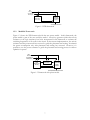
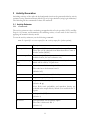
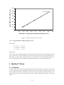
Power Model User’s Manual
(Version 1.1)
Prepared by Kara Poon
July 30, 2003
University of British Columbia
1
Table of Content
1
2
3
Introduction.......................................................................................................................................................... 4
1.1
What is new? ............................................................................................................................................... 4
1.2
Power Estimation Flow............................................................................................................................. 5
1.3
Framework................................................................................................................................................... 6
1.3.1
Original Framework...............................................................................................................................6
1.3.2
Modified Framework .............................................................................................................................7
Setup....................................................................................................................................................................... 8
2.1
Setup SIS ...................................................................................................................................................... 8
2.2
Setup VPR.................................................................................................................................................... 9
Activity Generation ..........................................................................................................................................11
3.1
3.1.1
Activity Estimator.....................................................................................................................................11
Commands.............................................................................................................................................11
3.2................................................................................................................................................................................12
3.2.1
Text Output File Format (.txt)............................................................................................................12
3.2.2
Activity Output File Format (.act).....................................................................................................13
3.3
4
Logic Simulator.........................................................................................................................................14
3.3.1
Vector Generator..................................................................................................................................14
3.3.2
Logic Simulator Commands...............................................................................................................14
3.3.3
Logic Simulator Output Format (.act) ..............................................................................................16
Modified T-VPack.............................................................................................................................................16
4.1
Commands .................................................................................................................................................16
4.2
Output Activity File Format (.ac2)........................................................................................................18
2
4.3
5
Output Function File Format (.fun)......................................................................................................18
Modified VPR ....................................................................................................................................................19
5.1
Commands .................................................................................................................................................19
5.2
Architecture File.......................................................................................................................................19
5.3
Power Analysis Output Files..................................................................................................................23
5.3.1
Power.echo ............................................................................................................................................23
5.3.2
ROUTINGPower.echo ........................................................................................................................24
5.3.3
LBPower.echo ......................................................................................................................................24
5.3.4
CLKPower.echo ...................................................................................................................................25
6
Conclusion...........................................................................................................................................................25
7
References ...........................................................................................................................................................26
3
1 Introduction
The power model is for non-commercial use only. For commercial use, please
contact the authors for their consent.
Note: This manual is for users who are familiar with SIS and VPR.
SIS is available at http://www-cad.eecs.berkeley.edu/Software/software.html
VPR can be downloaded at http://www.eecg.toronto.edu/~vaughn/vpr/vpr.html
The power model is built on top of SIS [7] and VPR CAD tool[1]. This manual focuses on
how to use the power model. For the algorithms and theories applied in the power model,
please refer to the references in section 6. In this document, the italicized words in angled
brackets <> should be replaced by appropriate file names, values, or options, while the
bolded words are keywords.
1.1 What is new?
The first version (version 1.0) of this power model was posted online in August 2002. Since
then, several changes have been made to the original power model. Here is the list of the
changes.
Update on version 1.1:
1. A logic simulator is added, so users can generate the switching activity for each node
in the benchmark circuits using logic simulation.
2. The power model has been revised. Here is a list of modified files.
read_arch.c
read_arch.h
power.c
power.h
vpr_types.h
The following is a list of specific changes:
read_arch.c
Added four new functions:
1. calc_num_buffer_stages(FO, desired_stage_effort)
2. calc_buffer_stage_effort(N, FO)
3. calc_internal_buffer_cap(FO, desired_stage_effort)
4. calc_internal_switch_caps(num_switch_types)
read_arch.h
Added two function declarations
1. calc_num_buffer_stages(FO, desired_stage_effort)
2. calc_buffer_stage_effort(N, FO)
Note: these are now used in power.c for calculating leakage within
buffers
4
power.c
1. Modified function find_routing_power() to also
consider the capacitance between cascaded buffer
stages.
2 Modified function find_logic_block_power. While
calculating the leakage power of a logic block, the
variable unused_CLB_leakage wasn't initialized to 0.0
causing the leakage power to be exagerated.
3. Modified function calculate_switch_leakage(). Fixed
calculation error.
power.h
Added two function declarations
1. find_cap
2. calculate_INV_cap
vpr_types.h
Added one member to the s_switch_inf structure:
1. float Cinternal
Node: this new member stores the internal capacitance of a cascaded
buffer for the given switch type
1.2 Power Estimation Flow
Figure 1.1 shows the power estimation flow employed for this project. First, benchmark
circuits were optimized and mapped using SIS [4]. The mapped netlist are imputed to either
an activity estimator or a logic simulator to generate activities for all nodes in the mapped
circuits. The activity estimator applies the Transitional Density Model [3] (a probabilistic
method) while the logic simulator applies logic simulation for activity generation.
Afterwards, TVPack groups the LUTs and registers into logic blocks based on the userspecified cluster size. Then, VPR is used to perform placement and routing for the circuits.
Each circuit is mapped to logic block array with sufficient logic blocks and pads. The VPR
router determines the minimum number of tracks per channel required to route the circuit.
The power estimation step has been incorporated in VPR to calculate power dissipation
based on the specified architecture [1].
5
Start
Vector Generator
(Stand-alone)
Input
stimuli
Netlist
Vector File
Logic Optimization
(SIS)
Technology Mapping
(SIS)
Activity Estimator
(Stand-alone)
Mapped
Netlist
Logic Simulator
(SIS)
Switching
Activity
Information
Packing
(modified TVPack)
Parametized
Architecture
Placement
(VPR)
Routing
(VPR)
Power Estimation
(IVPR)
Power
Estimates
End
Figure 1.1 Power estimation flow
1.3 Framework
This power model is built on top of The Versatile Place and Route (VPR) CAD tool. VPR is
a widely used placement and routing tool available for FPGA architectural studies. It is used
in combination with VPACK or TVACK, a logic block packing tool which packs each logic
block to capacity and minimizes the number of inter-cluster connections on the critical path
[1].
1.3.1
Original Framework
VPR has two components: a place and route tool, and a detailed area and delay model (See
Figure 1.2). The place and route tool maps a circuit to an FPGA. The area and delay
models estimate the area and critical path delay based on results from the place and route
tool. The two components interact with each other to determine the best placement and
routing for a user circuit. A description of the underlying FPGA architecture is provided to
the tool in the form of an architecture file, which contains information such as segment length,
connection topologies, logic block size and composition, and process parameters.
6
User
Circuit
Architecture
Description
Detailed
Area/Delay
Model
Place and
Route Tool
Area/Speed Estimates
Figure 1.2 VPR framework
1.3.2
Modified Framework
Figure 1.3 shows the VPR framework with the new power model. In this framework, the
power model is part of the area and delay model. An activity generator (either the activity
estimator or the logic simulator) has been incorporated in the framework to estimate the
switching frequencies of all nodes in the circuit. In the current implementation, the activity
estimator and the power model are not used to guide the placement and routing. It estimates
the power consumption only after placement and routing has occurred. However, it is
possible to use the power estimates to guide the placement and routing process in order to
optimize for power.
User
Circuit
Architecture
Description
VPR
(Place and
Route)
Activity
Generator
Detailed
Area/Delay/
Power
Model
Area/Speed/Power Estimates
Figure 1.3 Framework with power model
7
2 Setup
If you haven’t downloaded the powermodel, go to the following site and download the latest
version of the power model to the “powermodel” directory. The latest version is version 1.1.
http://www.ece.ubc.ca/~stevew/powermodel.html
Decompress the <powermodel_version.tar> file by typing
tar –xvf <powermodel_version.tar>
You
should
find
two
.tar
files:
powermodel_version_sis.tar
and
powermodel_version_vpr.tar under the powermodel_version directory. Note the version
in the directory and file names above indicates the current version number of the power
model. As you may have noticed, the current powermodel has two sections: one section of
the model is incorporated in SIS while the other section is incorporated in VPR. As a result,
these sections have to be installed separately.
The current version of the power model works on Solaris-based Unix machines, and it can be
compiled using g++ and gcc compilers. You may have to make modifications if you use other
operation systems or compilers. Follow the instructions below to download the software
2.1 Setup SIS
This section shows you how to install the vector generator and the logic simulator. The
vector generator is a stand-alone program, but the logic simulator is incorporated inside SIS.
Also, you may need to download other additional SIS packages, such as Flowmap[2], based
on the need of your research.
1.
Download and compile SIS by following the instruction at:
http://www-cad.eecs.berkeley.edu/Software/software.html
2.
Copy the powermodel_version_sis.tar file from the powermodel_version
directory to the parent directory of SIS.
3.
Decompress powermodel_version_sis.tar using the following command:
tar –xvf <powermodel_version_sis.tar>
Under the parent directory of SIS, you should have three new directories, which are
listed below and a script file, named setup_sis.pl.
Directory Name
Description
vecgen
Contains the source code of the vector generator (written in C)
actsim
Contains the source code of the logic simulator, which will be
moved as a sub-directory of the sis directory after running
setup_sis. pl.
sample
Contains sample scripts
8
4.
First of all, install the vector generator by executing the following commands
cd vecgen
compile_vecgen
cd ..
5.
Then, install the logic simulator by executing the setup_sis.pl script in the parent
directory using:
perl setup_sis.pl
6.
Recompile SIS with the logic simulator by typing:
make –i
You should have a SIS executable now.
Note: Sample scripts for SIS are available under the sample directory. These scripts are
provided to give you an example on how to use the logic simulator in SIS. To run the sample
script, go to the sample directory and type the following commands:
run_vecgen
<sis_executable> < sample_sis_command
2.2 Setup VPR
This section shows you how to install the activity estimator and the power model. The
activity estimator is a stand-alone program, but the power model is incorporated in VPR.
1.
Make a new directory called “powermodel”
2.
Go to the following site and download the version 4.30 of VPR to the powermodel
directory. The uncompressed version is recommended. The site is:
http://www.eecg.toronto.edu/~vaughn/vpr/vpr.html
3.
Copy the powermodel_version_vpr.tar under the powermodel_version directory
to the powermodel directory. Your powermodel directory should now contain two
.tar files (vpr_430.tar and powermodel_version_vpr.tar).
4.
Decompress the vpr_430.tar file first, and then decompress the
powermodel_version_vpr.tar file. You could use the following command to extract
the files.
tar -xvf <tar_file name>
Run the setup_powermodel Perl script. This script completes the compilation of the activity
estimator, T-Vpack and VPR automatically for you. The script assumes that you are running a
Solaris-based machine, and g++ and gcc compilers are available. If your compilers are different,
you may have to make some modifications to the makefile situated in each of the following
sub-directories.
9
Directory Name
Description
ace
contains the activity estimator source code (written in C++)
t-vpack
contains the T-Vpack source code (written in C)
vpr
contains the VPR source code (written in C)
Note: A demo is available with the power model source code to help you understand the
power estimation flow in VPR. To run the demo, execute the run_sample shell script in
your new powermodel directory after you finish the compilation.
10
3 Activity Generation
Switching activities of the nodes in the benchmark circuit can be generated either by activity
estimator (using Transition Density Model [3]) or by logic simulator (using logic simulation).
The following are the commands for these two methods.
3.1 Activity Estimator
3.1.1 Commands
The activity estimator takes a technology-mapped netlist of look-up-tables (LUTs) and flipflops in .blif format, and determines the switching activity of each node in the circuit by
applying the transition density model.
To run the activity estimator, use the following command:
ace -f <input.blif> -o <text output file> -n <activity output file> [other options]
Option
Description
-f <input.blif>
The input .blif file contains the netlist for a specific circuit.
These files can be obtained from Microelectronics Center of
North Carolina (MCNC).
-o <text output file>
The text output file (.txt) contains activity information (in a
readable format) for user’s reference only
-n <activity output The activity output file (.act) contains activity information
file>
which will be used by T-Vpack later
-e <float>
error tolerance for the static probability calculation
The value has to be between 0 and 1.
(default: 0.05)
-i <int>
max number of iterations (default: 10)
-p
output static probability only
-d
output transition density only
(default: -d -p)
Note: Both static probability and transition density are
available in the output files by default. You need both for TVpack.
-l <K>
look-up-table (LUT) size
(default: 4)
-s <float>
static probability for the primary inputs
The value is between 0 and 1.
(default: 0.5)
11
Option
Description
-t <float>
transition density of the primary inputs
(default: 0.5)
-r <float>
rise and fall time expressed as a value relative to the clock
period
This value is used for the low-pass filter mechanism of the
Transition Density Model [4][6].
(default: 0.1 which means the rise and fall time is 10% of the
clock frequency)
3.2
3.2.1
Text Output File Format (.txt)
File format:
Number of Luts: 10
Lut 0
Input: a
Static Probability:
Transition Probability:
Transition Density:
Input: b
Static Probability:
Transition Probability:
Transition Density:
Input: c
Static Probability:
Transition Probability:
Transition Density:
0.500000
0.500000
0.500000
0.500000
0.500000
0.500000
0.937500
0.117188
0.250000
Output: d
Static Probability:
0.984375
Transition Probability: 0.030762
Transition Density:
0.093750
Output is high for values: 1 2 3 4 5 6 7
.
.
.
Order of luts to be done 0 is lut 8
.
.
.
Now printing out the latch names and probability values.
latchNameIn: e latchNameOut: f inProb: 0.455149 outProb 0.455149
12
Description
The .txt file is for user’s reference only. It will not be used by T-Vpack or VPR. The first line
indicates the total number of look-up-tables (LUT) in the circuit. Then, the activity
information of each LUT is shown. In this example, a LUT with three inputs (a, b, and c)
and the output, d, is illustrated. The corresponding static probability, transition probability,
and transition density are also provided in this text file. The line with “Output is high for
values:” shows the numerical values of the logic functions when the output of the LUT is
high. After that, the order of the LUTs is listed in the file. Finally, the static probability
information of each latch in the circuit is printed at the end of the file.
3.2.2
Activity Output File Format (.act)
File format:
a
b
c
d
0.500000
0.500000
0.937500
0.984375
0.500000
0.500000
0.250000
0.093750
Description:
The .act file will be used by T-VPack later on. It contains the static probability and transition
density information of each node in the circuit. The first column is the name of the node;
the second and third columns list the corresponding static probability and transition density
of each node respectively.
13
3.3 Logic Simulator
The logic simulator takes a technology-mapped netlist to determine the switching activity of
each node in the circuit by applying logic simulation. It consists of two parts: a vector
generator and a logic simulator.
3.3.1
Vector Generator
The vector generator provides input vectors for the logic simulator. Users can specify their
own vectors instead, but it would be more convenient to generate the vector file
automatically using this vector generator. Users can pipe the output to a vector file as an
input file of the logic simulator.
To run the vector generator, use the following command:
vecgen <overall_activity> <num_of_primary_inputs> <num_of_vectors> <correlation>
> <vector_file>
Option
Description
<overall_activity>
Switching activity (transition density) at the primary
inputs
<num_of_primary_inputs> Number of primary inputs in the circuit
<num_of_vectors>
Number of vectors generated
Note: Using a larger number of vectors would increase
the simulation time, but the simulation results should
be more accurate.
<correlation>
The correlation between the primary inputs (The value
is between 0 and 1.)
A value of zero means the inputs are not correlated to
each other, whereas a value of one indicates the inputs
are 100% correlated.
3.3.2
Logic Simulator Commands
Before executing any logic simulator commands in SIS, the benchmark circuit (in .blif
format) has to be input to SIS first by using the following command:
read_blif <benchmark.blif>
14
Here is the list of logic simulator commands to set the delay of gates in the input circuit.
Command
Description
ls_zero_delay
Set the delay of all the gates to zero
ls_random_logic_delay <base_delay_value>
Randomly generate the delay for all the
gates based on the base_delay_value
ls_logic_delay <num>
Set the delay of all gates as a specific
value, num. (Unit : seconds)
After setting the delay value, run the logic simulator by typing:
ls_simulate_circuit –d <delay_portion> -f <filter_value>
<input_vector_file> <output_activity_file>
Option
Description
–d <delay_portion>
Both parameters are for modeling the filtration of
glitches by the gate.
-f <filter_value>
If a signal pulse is shorter than (d*gate_delay - f), then
the pulse would be filtered out by the gate. The
equation is derived by plotting the glitch width against
the gate delay.
Figure 3.1 shows the relationship between the glitch
width and the gate delay by assuming the glitch is
around 50% of the gate delay. Based on our HSPICE
simulation, the slope of the graph, d, is 0.89 and the yintercept, f, is 6.4e11. Users can define the values
according to the characteristics of their circuits.
Note: the number of simulator cycles is equal to the
number of vectors in your input vector files.
15
Glitch Width for 50% response (ns)
800
700
y = 0.89x - 64.01
600
500
400
300
200
100
0
0
100
200
300
400
500
600
700
800
900
Gate Delay - including wire and attached capacitances (ns)
Figure 3.1 Glitch width versus gate-delay
3.3.3
Logic Simulator Output Format (.act)
File format:
a
b
c
d
0.500000
0.500000
0.937500
0.984375
0.500000
0.500000
0.250000
0.093750
Description:
The output activity file generated by the logic simulator is the same as that generated by the
activity estimator of logic simulator. As a result, this output file can also be imported to TVPack later on. The first column is the name of the node; the second and third columns list
the corresponding static probability and transition density of each node respectively.
4 Modified T-VPack
4.1 Commands
T-VPack takes the same technology-mapped netlist (in .blif format) as the one used for the
activity estimator as its input and packs the look-up-table into clusters (logic blocks). For the
power model, T-VPack is employed to match the input switching activity information (.act
file) produced by the activity estimator in section 3 with the inputs and outputs of the logic
blocks.
16
To run T-VPack, use the following command:
t-vpack <input.blif> <output.net> -activity_in <input activity file>
-activity_out <output activity file>
-function_out <function output> [other options]
Please refer to the VPR user’s manual for the descriptions of the other options for this
command. To execute the power model, three additional options are required. These options
are listed below.
Option
Description
-activity_in <input activity file>
The input activity file (.act) which was
generated by the activity estimator
-activity_out
file>
<output
activity The output activity file (.ac2) which contains the
switching activity information for each logic
block. This file will be ported to VPR later.
-function_out <function output>
The function output file (.fun) which contains
the configuration bits for each look-up-table in
the logic blocks. This piece of information will
be used by VPR for power estimation.
17
4.2 Output Activity File Format (.ac2)
File Format:
global_net_probability clk 0.5
global_net_density clk 2.0
intercluster_probability a 0.5
intercluster_net_density a 0.2
intercluster_net_probability b
intercluster_net_density b 0.3
intercluster_net_probability z
intercluster_net_density z 0.5
.
.
.
subblock_probability z 0.5 0.1
subblock_density z 0.2 0.3 0.0
0.1
0.5
0.0 0.0 0.5 0.2 0.5
0.0 2.0 0.4 0.5
Description:
The .act2 will be used by VPR later on in the flow. Each global net in the design has its
corresponding global_net_probability and global_net_density lines. Following the keyword
global_net_probability or global_net_density, the probability or the transition density value
corresponding to the global net is listed. Nets that connect clusters (ie. use the generalpurpose routing) are listed using intercluster_net_probability and intercluster_net_density lines. The
format of each of these lines is the same as the global_net_probability (or global_net_density) lines.
Each subblock (LUT and/or FF) has its corresponding subblock_probability and
subblock_density lines. Following the keyword subblock_probability (or subblock_density), the
subblock name is listed. Then, the activities of all inputs (are then listed, followed by the
clock static probability (or clock transition density). Then, the probability (or transition
density) of the node between the LUT and flip-flop (if there is both a LUT and flip-flop
used within this subblock) is listed. (this number is 0 if a flip-flop is not used). Finally, the
activity of the output is listed.
4.3 Output Function File Format (.fun)
File Format:
subblock_function sb1 0011111111111111
subblock_function sb2 0011111111111111
Description:
The file will also be used by VPR in the power estimation flow. Following the keyword,
subblock_function, is the name of the subblock and the corresponding logic function
implemented in the subblock.
18
5 Modified VPR
5.1 Commands
To run VPR with the power model, use the following command:
vpr <circuit.net> <fpga.arch> <placed.out> <routed.out>
-activity_file <input activity file>
-function_file <input function file> [other VPR options]
Please refer to the VPR user manual [1] for other VPR options. Two additional options have
been added for power analysis.
Option
Description
-activity_file <input activity file>
The input activity file (.ac2) was created by TVPack
-function_file
file>
<input
function The input function file (.fun) was generated by
T-VPack
5.2 Architecture File
The following are the parameters in the architecture file for power analysis.
1.
global_clock_num <int>
Number of global clock network in the circuit
[The current version of power model can only handle one global H-tree clock
network]
2.
clock_network buffer_R: <float> buffer_Cin: <float> buffer_Cout: <float>
Rwire: <float> Cwire: <float> Cin_per_clb_clock_pin: <float>
The characteristics of a clock network, which includes:
Parameter
Description
buffer_R: <float>
Resistance of the clock buffer
buffer_Cin: <float>
Input capacitance of the clock buffer
buffer_Cout: <float>
Output capacitance of the clock buffer
Rwire: <float>
Wire resistance per unit segment length
Cwire: <float>
Wire capacitance per unit segment length
Cin_per_clb_clock_pin: <float>
Input capacitance for the clock input pin of
each logic block
19
3.
CLB_Cwire <float>
Wire capacitance per segment length for local connections inside the logic block
4.
temp <int> NMOS_NFS: <float> PMOS_NFS: <float>
NFS is the current fitting parameter that determines the slope of the sub-threshold
current-voltage characteristic. Specific NFS values are required for both NMOS and
PMOS transistors at a particular operation temperature [6].
These parameters are used for sub-threshold current calculation.
5.
Nmos Vth: <float> CJ: <float> CJSW: <float> CJSWG: <float> CGDO: <float>
COX: <float> EC: <float>
Characteristics of an NMOS transistor, which includes:
Parameter
Description
Vth: <float>
Threshold voltage (Unit: volt)
CJ: <float>
Area junction capacitance (Unit: F/m2)
CJSW: <float>
Sidewall junction capacitance (Unit: F/m)
CJSWG: <float>
Zero-bias gate-edge sidewall bulk junction capacitance
(Unit: F/m)
CGDO: <float>
gate-drain overlap capacitance (Unit: F/m)
COX: <float>
Gate oxide capacitance (Unit: F/m2)
EC: <float>
Piecewise carrier drift velocity
These parameters are used in the capacitance model and leakage current calculation
described in [6].
6.
Pmos Vth: <float> CJ: <float> CJSW: <float> CJSWG: <float>
CGDO: <float> COX: <float> EC: <float>
Characteristics of an PMOS transistor (similar to those for the NMOS transistor)
These parameters are used in the capacitance model and leakage current calculation
described in [6].
20
7.
poly Cpoly: <float> poly_extension: <float>
Characteristics of the polysilicon, which are:
Parameter
Description
Cpoly: <float>
capacitance of the polysilicon (Unit: F/m)
poly_extension: <float>
The extension of the polysilicon line (Unit: m)
Refer to Figure 5.1.
These parameters are used in the capacitance model described in [6].
DRAIN
G
A
T
E
SOURCE
W
poly_extension
Leff
Figure 5.1 Transistor layout
8.
min_transistor_size length: <float> width: <float>
Size of a minimum transistor
9.
Parameter
Description
length: <float>
channel length [see Leff in Figure 5.1] (Unit: m)
width: <float>
transistor width [see W in Figure 5.1] (Unit:m)
Vdd <float>
supply voltage (Unit: volt)
10.
Vswing <float>
swing voltage (Unit: volt)
21
11.
Vgs_for_leakage <float>
Gate-source voltage when the transistor is off. This parameter is used for leakage
current calculation. (Unit: volt)
12.
SRAM_leakage <float>
Leakage current inside the SRAM cell (Unit: Amp)
13.
short_circuit_power_percentage <float>
Short circuit power is represented as a percentage of the dynamic power within the
circuit. For example, if this value is set to 0.1, then short circuit power is modeled as
10% of the dynamic power dissipation
Note: Two architecture sample files (4lut_sanitized.arch and 4x4lut_sanitized.arch) are
provided in the samples directory to show you the format of the additional parameters.
However, the values in the sample files have been tailored to fulfill the non-disclosure
agreement that we signed with TSMC.
22
5.3 Power Analysis Output Files
The following are the formats of the four output files from VPR:
5.3.1
Power.echo
File format:
Critical_Path: 1.08982e-08
layout of FPGA: 2 x 2
operation temperature: 25
inputs: 6, outputs: 8, total clbs: 3, total global: 0
net num: 16, block num: 17
Power Analysis:
routing Power: 0.000826981 W(62.961876 percent)
Total Logic Block Power: 0.000173622 W(13.218604 percent)
Clock Power Dissipation: 0.000312861 W(23.819517 percent)
----------------------------------------Total Power Dissipation: 0.00131346 W
Leakage Power Analysis:
Routing Leakage Power: 1.99469e-05 W (1.518652 percent)
Logic Block Leakage Power: 2.74211e-06 W (0.208770 percent)
Clock Leakage Power: 0 W (0.000000 percent)
----------------------------------------Total Leakage Power: 2.2689e-05 W
(1.727421 percent of the total power dissipation)
Energy Analysis:
Routing Energy: 9.01257e-12 J
Logic Block Energy: 1.89216e-12 J
Clock Energy: 3.40961e-12 J
----------------------------------------Total Energy: 1.43143e-11 J
Power Analysis Completed
Description:
Power.echo first lists both the overall power (including dynamic, short-circuit and leakage
power) dissipation from the routing, logic blocks, and clock network. Then, it lists only the
leakage portion of the overall power. Finally, it includes an analysis on the energy dissipation
for the circuit.
23
5.3.2
ROUTINGPower.echo
File format:
net 0: 0.000113028 W
Description:
ROUTINGPower.echo records the power dissipation of each net in the circuit. Following the
keyword, net, is the net number and the power dissipation of that particular net
5.3.3
LBPower.echo
File format:
******** Logic Block Power Analysis
*******
block number: 1
subblock name:a
subblock power: 1.02171e-05
subblock name:b
subblock power: 1.07384e-05
subblock name:c
subblock power: 1.02171e-05
subblock name:d
subblock power: 1.23027e-05
Number of unused subblocks: 0
Leakage power from unused subblocks: 0 W
Power dissipated by this block: 6.50786e-05 w
W
W
W
W
.
.
.
==========================================================
Total Logic Block energy: 0.000170879 w
Description:
LBPower.echo contains information regarding the power dissipated by each logic block.
Following with the keyword, block number, is the number of a specific block. Then, a list of
the subblocks included in this block is shown. After that, the number of unused subblocks in
this block and the amount of leakage power from those unused subblocks are provided. The
power dissipated by this block consists of the power dissipated by subblocks and local
connections inside the block. Finally, the total power dissipated by all the logic blocks
(CLBs) in the circuits is listed.
24
5.3.4
CLKPower.echo
File format:
Clock Network 0: Power= 0.000312861, Delay=8.00063e-11
Description:
Currently, the power model can only handle one clock network. However, multiple clock
networks may be included in this power model in the future. To investigate the power
consumption of each clock network, the CLKPower.echo is provided. Following the keyword,
Clock Network, is the number of this particular clock network, its power dissipation (in Watt),
and the clock delay (in seconds). The clock delay is calculated by adding the clock buffer
delay with the clock wire delay along the path from the clock input to the input of a CLB.
The clock skew has not been considered in this model. The clock delay provided is only a
rough estimation.
6 Conclusion
This power model is developed to establish a practical platform for future research on power
analysis and optimization within FPGAs. It consists of a vector generator, logic simulator,
activity estimator, and a power model. We understand that there is always room for
improvement for us to build a more robust power model. Your feedbacks and comments
about the future development of this power model is invaluable for our team and the FPGA
research community. Please feel free to let us know about your opinions.
Thank you for you interest in our power model and good luck on your research.
25
7 References
[1] V.Betz, VPR and T-VPack User’s Manual, ver 4.30, March 2000.
[2] J. Cong and Y.Ding, “Flowmap: An Optimal Technology Mapping Algorithm for Delay
Optimization in Lookup-Table Based FPGA Designs,” IEEE Trans. on ComputerAided Design of Integrated Circuits and Systems, Vol. 13, No. 1, pp.1-12, January 1994.
[3] F.N. Najm, “Transition Density, A New Measure of Activity in Digital Circuits,” Texas
Instruments Technical Report #7529/0032, August 1991.
[4] F.N. Najm, “Low-pass Filter for Computing the Transition Density in Digital Circuits,”
IEEE Transactions on Computer-Aided Design, vol. 13, no. 9, pp. 1123-1131,
September 1994.
[5] K.Poon, A.Yan, S.J.E. Wilton, “A Flexible Power Model for FPGAs,” in International
Conference on Field-Programmable Logic and Applications, September 2002.
[6] K.K.W. Poon, “Power Estimation For Field Programmable Gate Arrays,” Master’s
Thesis, University of British Columbia, August 2002.
[7] E.M. Sentovich, K.J. Singh, C. Moon, H. Savoj, R. K. Brayton, and A.L. SangiovanniVincentelli, “Sequential Circuit Design Using Synthesis and Optimization,” ICCD,
pp.328-333, 1992.
26


![[U4.53.01] Opérateur DYNA_NON_LINE](http://vs1.manualzilla.com/store/data/006362356_1-a18ba5203ff6a78bf38356682490341a-150x150.png)


![[U4.53.01] Opérateur DYNA_NON_LINE](http://vs1.manualzilla.com/store/data/006361140_1-c6823d371505afbfe108409e7ca50202-150x150.png)