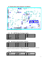
1
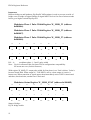
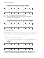
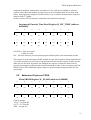
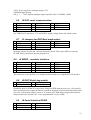
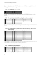
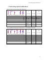
DSP2
User’s Manual
Copyright © 2001
University of Maribor
Faculty of Electrical Engineering and Computer Science
Institute of Robotics
Smetanova ulica 17
2000 MARIBOR
SLOVENIA
http://www.ro.feri.uni-mb.si/Welcome.html-l2
Manual version:
Firmware version:
PCB version:
Bios version:
Terminal version:
V 0.704.17
V0.80
V1.00
V1.10
V1.1a
(March 13, 2001)
(April 17, 2000)
(Februar 12, 2000)
(Mai 12, 2000)
(Jan 23, 2000)
Contents
Contents
1.
DSP board overview ___________________________________________________ 1
2.
Simplified Function Diagram ____________________________________________ 2
3.
DSP2 Memory Map ____________________________________________________ 3
4.
Interrupts ____________________________________________________________ 4
5.
FPGA Registers Reference ______________________________________________ 5
5.1
AD Unit _________________________________________________________
5.1.1
AD Operation _________________________________________________
Register ADCTRL (address 0x900002 - WRITE) ___________________________
Register AD0 (address 0x900001 - READ) ________________________________
Registers AD1 (address 0x900002), AD2 (address 0x900003), AD3 (address
0x900004)__________________________________________________________
Registers AD1 (address 0x900002), AD2 (address 0x900003), AD3 (address
0x900004)__________________________________________________________
ii
5
5
6
6
7
7
2
5.2
I C EEPROM____________________________________________________ 8
Register W_I2C (address 0x90000E) ____________________________________ 8
Register R_I2C (address 0x90000E)____________________________________ 8
5.3
Asynchronous Serial Communications Interface _______________________ 9
Receiver Status Register RS_STAT (address 0x900006) _____________________ 9
Serial Control Register CRTL (address 0x900004) _________________________ 9
Serial Receive Register RX0 (address 0x900005) _________________________ 10
Serial Transmit Register TX0 (address 0x900003) _________________________ 10
5.4
Three Phase Pulse Width Modulator ________________________________
Modulator Period Register W_MOD_PER (address 0x900005) _______________
Modulator Dead Time Set Register W_MOD_TM (address 0x900009) _________
Modulator Phase 1 Pulse Width Register W_MOD_T1 (address 0x900006) _____
Modulator Phase 2 Pulse Width Register W_MOD_T2 (address 0x900007) _____
Modulator Phase 3 Pulse Width Register W_MOD_T3 (address 0x900008) _____
Modulator Status Register W_MOD_STAT (address 0x90000F) ______________
5.5
FLASH PROM Interface__________________________________________ 13
Flash PROM Register W_FLASH (address 0x90000F) _____________________ 13
5.6
Analog Output Unit ______________________________________________
Analog Output 0 Register DA0 (address 0x900000) ________________________
Analog Output 1 Register DA1 (address 0x900001) ________________________
Analog Output Status Register DASTAT (address 0x900000) ________________
5.7
Incremental Encoder Interface _____________________________________ 14
Incremental Encoder Position Read Register R_INC_POS (address 0x900007) __ 14
Incremental Encoder Time Read Register R_INC_TIME (address 0x900008)____ 15
5.8
Extension IO pins on FPGA _______________________________________ 15
Flash PROM Register W_FLASH (address 0x90000F) _____________________ 15
5.9
CAN Interface___________________________________________________
Write CAN Register W_CAN (address 0x900800F) ________________________
Read CAN Register R_CAN (address 0x900800F) _________________________
CAN Control Register W_CAN CTRL (address 0x9000A) __________________
11
11
11
12
12
12
12
13
13
14
14
16
16
16
16
Contents
CAN Status Register W_CAN STAT (address 0x900009) ___________________ 16
6.
Connectors and Jumpers Locations ______________________________________ 17
6.1
P1 – IGBT Bridge Analogue inputs __________________________________ 17
6.2
P3 Serial communication (RS232) ___________________________________ 17
6.3
P4 Incremental encoder input ______________________________________ 17
6.4
P5 IGBT Bridge – digital I/O _______________________________________ 18
6.5
J1 Analogue outputs, analogue inputs________________________________ 18
6.6
J2 DSP serial communication_______________________________________ 19
6.7
J3 Jumpers for DSP Boot mode select________________________________ 19
6.6
J4 MPSD – emulator interface______________________________________ 19
6.8
J5 DSP Watch dog enable__________________________________________ 19
6.9
J6 Serial interface RS485 __________________________________________ 19
6.10
J7 EEPROM write enable _________________________________________ 20
6.11
J8 optically isolated (three inputs and one output) _____________________ 20
6.12
J9 CAN interface (before and after line driver), 16 I/O user defined pins __ 20
6.13
J10 FPGA extension pins __________________________________________ 20
6.14
J11 FPGA JTAG interface _________________________________________ 21
6.15
J12 FPGA external programming interface ___________________________ 21
6.16
J13 two DSP timer outputs_________________________________________ 21
6.17
Power supply ____________________________________________________ 21
7.
Fast analog inputs modifications_________________________________________ 23
8.
References___________________________________________________________ 25
Tables
Table 1: DSP2 Memory Map ....................................................................................................3
Table 2: FPGA Register Map....................................................................................................5
Table 3: AD3 Input selection table ...........................................................................................6
Table 4: DSP2 Power supply connections ..............................................................................21
Table 5: Power supply signals explanation .............................................................................22
Table 6: Normal (current) fast analogue input configuration .................................................23
Table 7: Modified fast analogue input configuration for use with MiniSKiiP IGBT module 23
Figures
Figure 1: DSP2 Function Diagram............................................................................................2
Figure 2: Analog Input Configuration.......................................................................................5
Figure 3: I2C Implementation Detail ........................................................................................8
Figure 4: Asynchronous Serial Communications Baud Rate Select .........................................9
Figure 5: Connector with Test Pins on DSP2 Board Detail ....................................................16
Figure 6: Connectors and Jumpers Locations .........................................................................17
Figure 7: Power Fail Input Detail............................................................................................18
iii
DSP board overview
1. DSP board overview
The DSP-2 board is a high performance, floating point digital signal processor (DSP) based
inverter controller designed primarily to control a three-phase AC motor. The board is based
on Texas Instruments TMS320C32 DSP and Field Programmable Gate Array (FPGA)
XCS40-4PQ240C member of Xilinx Spartan Family.
• DSP TMS320C32-60MHz
o DSP serial interface
o Two timer general purpose io pins
o DSP MPSD interface for XDS510 emulator
• FLASH 256K x 8 - 70ns
• SRAM 128K x 32 0WS
• 4 channel simultaneous 12bit A/D with serial output
o Conversion and transfer to register in FPGA 2,6µs for all four channels
o One channel has unipolar input range 0 to 4.095V or 0 to 40,95mA with
100OHM shunt resistor (udc)
o Two have bipolar input range –2.096 to 4.094V or -40,96mA to 40.94mA
with 100OHM shunt resistor
o One channel has input multiplexer to select one of eight voltage input signals
o First order input RC filters (time constant 33µs for i1 and i3 and 100µs for
udc)
• Two channel 12bit D/A converter with serial input and unipolar output 0 to 4V
• RS232 full duplex interface with fixed Baud Rate (38400kBd 8bits ,1stop ,No parity)
• RS485 interface (not implemented in this firmware version (April 17, 2000)
• RS422 receiver for incremental encoder
• Three logic inputs and one output – all optically isolated (12V passive)
• Bridge protection circuit
o Interlock between bottom and top IGBT activation and dead time
o Minimum pulse width, minimum pause width
o In the presence of fault signal the bridge is shut down unconditionally
• Three phase synchronous pulse width modulator
o Twelve bit up/down counter for triangle generation
o Symmetrical output pulses
o 66.6ns time resolution
o can generate interrupt pulses ones or twice in one modulator period
• Incremental encoder speed measurement with improved MT method
o 66.6ns time resolution
o Position register contain position increment during sampling period
o Time register contain relative time (in one modulator period) of last position
change
o Booth registers are saved on interrupt and are available until next interrupt
• Stand alone operation. Program is preloaded in FLASH.
• Operation with personal computer
o Code Composer software development environment
o Standard RS232 serial interface (38400Bd) and Terminal software
o MPSD interface for XDS510 emulator
o Multipoint communications RS485 and CAN (not implemented yet)
• Board dimensions 161 x 130 mm
1
Simplified Function Diagram
2. Simplified Function Diagram
Power supply
supervisor
32
DSP
TMS320C32-60
EEPROM
4...256kb
ADM232A
RS232
interface
RS485
interface
LTC485
Boundary
Scan Logic
DT
H/W
INTERLOCK
MIN.
DEADTIME
PERIOD
XilinX
XCS40PQ240
A/D
interface
A/D A/D A/D A/D
400kS/s 12bit 12bit 12bit 12bit
INCR. ENC.
interface
D/A
interface
RS422
I/O
D/A D/A
12bit 12bit
MUX
LPF
LPF
LPF
LPF
0..10V
10V
10V
8x 10V
Figure 1: DSP2 Function Diagram
2
+-
0..5V -5..5V 0..5V
INVERTER
CAN
interface
XDS510
MPSD Port
INC.ENC.
SAE81C90
EEPROM
interface
16
10 GP I/O PINS
2
I C
JTAG
RS485
RS232
CAN 16 GP I/O
SRAM 0WS
128K x 32
8
SERIAL PORT
FLASH
256 x 8
3xIN 1xOUT
DSP2 Memory Map
3. DSP2 Memory Map
Table 1: DSP2 Memory Map
0x810000 … 0x82FFFF
0x880000 … 0x89FFFF
0x900000 … 0x900FFF
FLASH
RAM
FPGA
128K*8 bits
128K*32bits
*16bits
3
Interrupts
4. Interrupts
External interrupts are controlled by firmware in FPGA. In this version (April 17, 2000) only
one interrupt (INT0) are generated by three phase pulse width modulator. Interrupt can be
generated once or twice in one modulator period. Interrupt INT1 is used for boot mode
select.
4
FPGA Registers Reference
5. FPGA Registers Reference
Table 2: FPGA Register Map
Address
0x900000
0x900001
0x900002
0x900003
0x900004
0x900005
0x900006
0x900007
0x900008
0x900009
0x90000A
0x90000B
0x90000C
0x90000D
0x90000E
0x90000F
0x900800 …
0x9008ff
5.1
WRITE
DA0
DA1
ADCRTL
TX0
CTRL
W_MOD_PER
W_MOD_T1
W_MOD_T2
W_MOD_T3
W_MOD_TM
W_CAN_CTRL
Reserved
Reserved
Reserved
W_I2C
W_FLASH
W_CAN
READ
DA_STAT
AD0 (udc)
AD1 (i1)
AD2 (i3)
AD3 (mux)
RX0
RS_STAT
R_INC_POS
R_INC_TIME
R_CAN_STAT
Reserved
Reserved
Reserved
Reserved
R_I2C
R_MOD_STAT
R_CAN
AD Unit
Figure 2: Analog Input Configuration
Note: -Analogue VCC is separated
-Internal voltage reference is used
-Vss pin is connected to –5V for bipolar operation i1,i3!
-Leading bits for udc are zero except MSB (bit 15) which is 1 during A/D conversion
(unsigned extension to 16 bits)
-For currents measurement (i1 and i3) leading bits (bit 15, 14, 13 and 12) are equal to
bit 11 (signed extension to 16 bit)
-User must extend read value to 32 bits depend on data type
5.1.1 AD Operation
AD conversion is started by interrupt request. After approximately 2.5 microseconds
simultaneous conversion of all four channels is finished. You have time to next interrupt to
read converted data.
Fourth channel (AD3) is connected to multiplexer which choose one of eight analogue
inputs. Decision is made with register ADCTRL and bits 0 to 2.
Note: In current version of FPGA firmware (April, 17 2000) A/D conversion is started when
write to ADCTRL register appear.
5
FPGA Registers Reference
Register ADCTRL (address 0x900002 - WRITE)
15
14
13
12
11
10
9
8
NC
NC
NC
NC
NC
NC
NC
NC
-/W
-/W
-/W
-/W
-/W
-/W
-/W
-/W
7
6
5
4
3
2
1
0
NC
NC
NC
NC
NC
AD_MUX2
AD_MUX1
AD_MUX0
-/W
-/W
-/W
-/W
-/W
-/W
-/W
-/W
Table 3: AD3 Input selection table
ADCTRL
0x0000
0x0001
0x0002
0x0003
0x0004
0x0005
0x0006
0x0007
AD_MUX2
0
0
0
0
1
1
1
1
AD_MUX1
0
0
1
1
0
0
1
1
AD_MUX0
0
1
0
1
0
1
0
1
Analog
CH0
CH1
CH2
CH3
CH4
CH5
CH6
CH7
Note: -Use 0 for all unused bits for future FPGA configurations compatibility.
-NC means not care (for this firmware)
Register AD0 (address 0x900001 - READ)
15
14
13
12
11
10
9
8
AD_BUSY
0
0
0
B11
B10
B9
B8
R/-
R/-
R/-
R/-
R/-
R/-
R/-
R/-
7
6
5
4
3
2
1
0
B7
B6
B5
B4
B3
B2
B1
B0
R/-
R/-
R/-
R/-
R/-
R/-
R/-
R/-
AD_BUSY:
A/D converter status:
1 = conversion is in progress (You must wait until bit is set 0!)
0 = conversion finished
Note: Same busy bit (AD0.AD_BUSY) is used for all four analogue converters because the
conversion is simultaneous.
B0 – B15:
6
16-bit unsigned data udc. IF AD_BUSY is 0!
FPGA Registers Reference
Registers AD1 (address 0x900002), AD2 (address 0x900003), AD3
(address 0x900004)
15
14
13
12
11
10
9
8
B11
B11
B11
B11
B11
B10
B9
B8
R/-
R/-
R/-
R/-
R/-
R/-
R/-
R/-
7
6
5
4
3
2
1
0
B7
B6
B5
B4
B3
B2
B1
B0
R/-
R/-
R/-
R/-
R/-
R/-
R/-
R/-
AD1, AD2 and AD3 are data registers that contain AD conversion results. Bit 11 is a sign bit
and is extended to bits 12 thru 15 to form 2nd complement.
Note: Same busy bit (AD0 – BUSY) is used for all four analog converters because the
conversion is simultaneous.
B0 – B15:
16-bit unsigned data udc. IF AD_BUSY is 0!
Registers AD1 (address 0x900002), AD2 (address 0x900003), AD3
(address 0x900004)
15
14
13
12
11
10
9
8
B11
B11
B11
B11
B11
B10
B9
B8
R/-
R/-
R/-
R/-
R/-
R/-
R/-
R/-
7
6
5
4
3
2
1
0
B7
B6
B5
B4
B3
B2
B1
B0
R/-
R/-
R/-
R/-
R/-
R/-
R/-
R/-
AD1, AD2 and AD3 are data registers that contain AD conversion results. Bit 11 is a sign bit
and is extended to bits 12 thru 15 to form 2nd complement.
Note: Same busy bit (AD0 – BUSY) is used for all four analog converters because the
conversion is simultaneous.
7
FPGA Registers Reference
5.2
I 2C EEPROM
Register W_I2C (address 0x90000E)
15
14
13
12
11
10
9
8
NC
NC
NC
NC
NC
NC
NC
NC
-/W
-/W
-/W
-/W
-/W
-/W
-/W
-/W
7
6
5
4
3
2
1
0
NC
NC
NC
NC
NC
NC
SDA
SCL
-/W
-/W
-/W
-/W
-/W
-/W
-/W
-/W
Bit 0: connected to SCL line
Bit 1:
0 SDA pin is in THREE STATE (external pull-up resistor apply high logic level)
1 SDA shorted to ground low logic level
Note: NC means not care (for this firmware)
For future compatibility write always write 0 to NC bits
Register R_I2C (address 0x90000E)
15
14
13
12
11
10
9
8
1
1
1
1
1
1
1
1
R/-
R/-
R/-
R/-
R/-
R/-
R/-
R/-
7
6
5
4
3
2
1
0
1
1
1
1
1
1
SDA
1
R/-
R/-
R/-
R/-
R/-
R/-
R/-
R/-
Bit 1: connected to SDA line
Note: Use only level of Bit 1 (SDA) for future compatibility.
I2C sck
i0
D
scl
Q
bscl
P13
INV
C
OBUF
OPAD
FD
i1
D
wr_i1c
Q
sda
E
INV
bsda
P15
GND
FD
OBUFE
IOPAD
XU1
rd_i1c
E
U13
o1
BUFE
IBUF
Figure 3: I2C Implementation Detail
8
I2C sda
C
FPGA Registers Reference
Because pin compatibility of serial I2C EEPROMs any type of memory in 8 pin SO package
can be used (for example M24C01, M24C02, M24C04, M24C08, M24C16, M24C32,
M24C64, M24C128, M24C256 or M24512 – ST Microelectronics) On DSP2 M24C04 is
implemented (512 bytes x 8 bits).
Write Control (WC)
This input signal is useful for protecting the entire contents of the memory from inadvertent
write operations. Write operations are disabled to the entire memory array when Write
Control (WC) is driven High. (Jumper J7 is not inserted) When Write Control (WC) is driven
High, Device Select and Address bytes are acknowledged, Data bytes are not acknowledged.
5.3
Asynchronous Serial Communications Interface
Receiver Status Register RS_STAT (address 0x900006)
15
14
13
12
11
10
9
8
1
1
1
1
1
1
1
1
R/-
R/-
R/-
R/-
R/-
R/-
R/-
R/-
7
6
5
4
3
2
1
0
TRF
RRF
OV
FE
1
1
SDA
1
R/-
R/-
R/-
R/-
R/-
R/-
R/-
R/-
FE: framing error (invalid stop bit)
OV: overflow (previous byte is not read while new received)
RRF: receive register full (unread byte is in receive register)
All three bits are cleared when receive register is read
TRF: transmit register full
Serial Control Register CRTL (address 0x900004)
15
14
13
12
11
10
9
8
NC
NC
NC
NC
NC
NC
NC
NC
-/W
-/W
-/W
-/W
-/W
-/W
-/W
-/W
7
6
5
4
3
2
1
0
SRG7
SRG6
SRG5
SRG4
SRG3
SRG2
SRG1
SRG0
-/W
-/W
-/W
-/W
-/W
-/W
-/W
-/W
SRG7…0:
SELECT Baud Rate
Note: Use 0 for all unused bits for future FPGA configurations compatibility.
NC means not care (for this firmware)
Figure 4: Asynchronous Serial Communications Baud Rate Select
SRG BaudRate1
BaudRate2 Error[%]
9
FPGA Registers Reference
SRG BaudRate1
195
9600
98
19200
49
38400
33
57600
16
115200
8
230400
4
460800
BaudRate2 Error[%]
9615.38
0.16
19132.65
0.35
38265.31
0.35
56818.18
1.36
117187.50
-1.73
234375.00
-1.73
468750.00
-1.73
Note: This feature is not implemented in firmware version April 17, 2000 in FPGA.
Serial Receive Register RX0 (address 0x900005)
15
14
13
12
11
10
9
8
1
1
1
1
1
1
1
1
R/-
R/-
R/-
R/-
R/-
R/-
R/-
R/-
7
6
5
4
3
2
1
0
B7
B6
B5
B4
B3
B2
B1
B0
R/-
R/-
R/-
R/-
R/-
R/-
R/-
R/-
B7 ... 0: received byte
Serial Transmit Register TX0 (address 0x900003)
15
14
13
12
11
10
9
8
NC
NC
NC
NC
NC
NC
NC
NC
-/W
-/W
-/W
-/W
-/W
-/W
-/W
-/W
7
6
5
4
3
2
1
0
B7
B6
B5
B4
B3
B2
B1
B0
-/W
-/W
-/W
-/W
-/W
-/W
-/W
-/W
B7…0:
byte to transmit
Note: Use 0 for all unused bits for future FPGA configurations compatibility.
NC means not care (for this firmware)
Receive and transmit registers are double buffered. This mean that another character can be
received while previous one is in the receive register. You must read previous character just
before next one is complete received. Same thing is with transmit register. When the output
shift register is empty then serial transmit register is empty for new character in less than 1 /
(16 * BAUD RATE). Transmission time for one character is 10 / BAUD RATE.
10
FPGA Registers Reference
5.4
Three Phase Pulse Width Modulator
Modulator Period Register W_MOD_PER (address 0x900005)
15
14
13
12
11
10
9
8
NC
NC
NC
NC
B11
B10
B9
B8
-/W
-/W
-/W
-/W
-/W
-/W
-/W
-/W
7
6
5
4
3
2
1
0
B7
B6
B5
B4
B3
B2
B1
B0
-/W
-/W
-/W
-/W
-/W
-/W
-/W
-/W
B11…0:
modulator period
Note: Use 0 for all unused bits for future FPGA configurations compatibility.
NC means not care (for this firmware)
PERIOD register: Half period of PWM is equal PERIOD + 1, while whole period is
2*(PERIOD+1). Values for this register must be between 2 and 2000. Unit for period is 1 /
60MHz * 4 = 66.6ns
Modulator Dead Time Set Register W_MOD_TM (address
0x900009)
15
14
13
12
11
10
9
8
NC
NC
NC
I_EN
OM
RELAY
BOFF
BON
-/W
-/W
-/W
-/W
-/W
-/W
-/W
-/W
7
6
5
4
3
2
1
0
B7
B6
B5
B4
B3
B2
B1
B0
-/W
-/W
-/W
-/W
-/W
-/W
-/W
-/W
B7…0: modulator period
Note: Use 0 for all unused bits for future FPGA configurations compatibility.
NC means not care (for this firmware)
TM register:
B7 ... 0: dead time between top and bottom switch in bridge (another hardware
protection implemented in GAL circuit limit dead time to about 3.5micro second minimum RC time constant). TM is used because RC constant is not enough accurate - approximately
10%. Unit is 50ns. Value must be between 0 and 255.
Same register contain logic output bits:
B_ON: bridge on
B_OFF: bridge off
RELAY: relay (for by-pass charge resistor for DC link)
OM: -0 single interrupt request in one period of PWM
-1 interrupt request in each half-period of PWM
I_EN: PWM interrupt enable
11
FPGA Registers Reference
Important:
Between bridge on and hardware flip-flop RC differentiator is used to prevent override of
bridge error or bridge off signal. Bridge on signal MUST be low few tens of microseconds
before go to high to switch flip-flop ON.
Modulator Phase 1 Pulse Width Register W_MOD_T1 (address
0x900006)
Modulator Phase 2 Pulse Width Register W_MOD_T2 (address
0x900007)
Modulator Phase 3 Pulse Width Register W_MOD_T3 (address
0x900008)
15
14
13
12
11
10
9
8
NC
NC
NC
NC
B11
B10
B9
B8
-/W
-/W
-/W
-/W
-/W
-/W
-/W
-/W
7
6
5
4
3
2
1
0
B7
B6
B5
B4
B3
B2
B1
B0
-/W
-/W
-/W
-/W
-/W
-/W
-/W
-/W
B11…0:
modulator phase 1, 2 and 3 pulse width
Note: Use 0 for all unused bits for future FPGA configurations compatibility.
NC means not care (for this firmware)
With register W_MOD_T1 output pulse width for first phase is set. Unit is 66.6ns. Value is
between 0 and 2000. When output is 1 TOP IGBT is active, when output is 0 active is
bottom one. When transition of signal appear then immediately active IGBT is inactivated
and then, after dead time, another one is activated.
Modulator Status Register W_MOD_STAT (address 0x90000F)
15
14
13
12
11
10
9
8
B_EN
1
1
1
1
1
1
1
R/-
R/-
R/-
R/-
R/-
R/-
R/-
R/-
7
6
5
4
3
2
1
0
1
1
1
1
1
1
1
1
R/-
R/-
R/-
R/-
R/-
R/-
R/-
R/-
Status of bridge:
B_EN: bridge enable
12
FPGA Registers Reference
With bridge on and bridge off you can toggle hardware flip-flop. Bridge enable show the
state of this flip-flop. State of the flip-flop can also be changed with error signal from IGBT
Bridge to zero. Error signal in Mini SKiiP bridge includes: over current, earth connection
(sum of phase currents must be zero), over heat...
5.5
FLASH PROM Interface
Flash PROM Register W_FLASH (address 0x90000F)
15
14
13
12
11
10
9
8
NC
NC
NC
NC
B11
B10
B9
B8
-/W
-/W
-/W
-/W
-/W
-/W
-/W
-/W
7
6
5
4
3
2
1
0
NC
NC
NC
NC
XX1
XX6
A17_F
A16_F
-/W
-/W
-/W
-/W
-/W
-/W
-/W
-/W
Logical outputs:
A16_F:
A16 FLASH
A17_F:
A17 FLASH
These two bits are for change page in FLASH. Because only 8 bit data width FLASH is only
used for boot-loader program. After download FLASH is disabled. In future user program
can be downloaded from FLASH.
XX6: test pin xx6
XX1: test pin xx1
Note: Use 0 for all unused bits for future FPGA configurations compatibility.
NC means not care (for this firmware)
For XX6 and XX1 see section FPGA extension pins.
5.6
Analog Output Unit
Analog Output 0 Register DA0 (address 0x900000)
15
14
13
12
11
10
9
8
NC
NC
NC
NC
B11
B10
B9
B8
-/W
-/W
-/W
-/W
-/W
-/W
-/W
-/W
7
6
5
4
3
2
1
0
B7
B6
B5
B4
B3
B2
B1
B0
-/W
-/W
-/W
-/W
-/W
-/W
-/W
-/W
B11… B0:
12 bit unsigned value (0 = 0V, 4095=4.095V)
Note: Use 0 for all unused bits for future FPGA configurations compatibility.
NC means not care (for this firmware)
13
FPGA Registers Reference
Analog Output 1 Register DA1 (address 0x900001)
15
14
13
12
11
10
9
8
NC
NC
NC
NC
B11
B10
B9
B8
-/W
-/W
-/W
-/W
-/W
-/W
-/W
-/W
7
6
5
4
3
2
1
0
B7
B6
B5
B4
B3
B2
B1
B0
-/W
-/W
-/W
-/W
-/W
-/W
-/W
-/W
B11… B0:
12 bit unsigned value (0 = 0V, 4095=4.095V)
Note: Use 0 for all unused bits for future FPGA configurations compatibility.
NC means not care (for this firmware)
Analog Output Status Register DASTAT (address 0x900000)
15
14
13
12
11
10
9
8
DA_BUSY
1
1
1
1
1
1
1
R/-
R/-
R/-
R/-
R/-
R/-
R/-
R/-
7
6
5
4
3
2
1
0
1
1
1
1
1
1
1
1
R/-
R/-
R/-
R/-
R/-
R/-
R/-
R/-
DA_BUSY: 1-interface busy
When data is writen to second D/A register serial transmit to D/A converter is started and bit
15 in DASTAT is set to 1. This bit is cleared to zero when both channels are transmitted and
interface is ready for new data. When bit 15 in DASTAT is set, writing to any of DA0 or
DA1 is prohibited and can cause transmit of void data to DA converter!
5.7
Incremental Encoder Interface
Incremental Encoder Position Read Register R_INC_POS (address
0x900007)
15
14
13
12
11
10
9
8
B11
B11
B11
B11
B11
B10
B9
B8
R/-
R/-
R/-
R/-
R/-
R/-
R/-
R/-
7
6
5
4
3
2
1
0
B7
B6
B5
B4
B3
B2
B1
B0
R/-
R/-
R/-
R/-
R/-
R/-
R/-
R/-
On each interrupt value from position counter is transferred to this register and COUTER IS
CLEARED. Position must be externally accumulated. Value is 16 bit long in 2'nd
14
FPGA Registers Reference
complement notation. And must be extended to 32 bits with sign and added to software
position value. Maximal number of pulses between two interrupts must be less than 2048
pulses. Input signal are sampled 15 million times every second so maximal input frequency
must be under 3.75MHz.
In this version of FPGA firmware counter has eleven data bits and sign.
Incremental Encoder Time Read Register R_INC_TIME (address
0x900008)
15
14
13
12
11
10
9
8
STATUS
0
0
0
B11
B10
B9
B8
R/-
R/-
R/-
R/-
R/-
R/-
R/-
R/-
7
6
5
4
3
2
1
0
B7
B6
B5
B4
B3
B2
B1
B0
R/-
R/-
R/-
R/-
R/-
R/-
R/-
R/-
STATUS: 1: data are invalid
0: data are valid
B11…B0: time between previous interrupt pulse and last pulse from incremental encoder
This register is used with improved MT method for speed measurement. Most significant bit
is set when no pulses are received (in last period) from incremental encoder. In this case the
other bits are not valid. If position was changed, this register contains the time between
previous interrupt pulse and last pulse from incremental encoder. Units are same as units for
PWM (66.6ns). This additional register improves speed measurement particularly for low
speed range.
5.8
Extension IO pins on FPGA
Flash PROM Register W_FLASH (address 0x90000F)
15
14
13
12
11
10
9
8
NC
NC
NC
NC
B11
B10
B9
B8
-/W
-/W
-/W
-/W
-/W
-/W
-/W
-/W
7
6
5
4
3
2
1
0
NC
NC
NC
NC
XX1
XX6
A17_F
A16_F
-/W
-/W
-/W
-/W
-/W
-/W
-/W
-/W
Logical outputs:
A16_F: A16 FLASH
A17_F: A17 FLASH
XX6: test pin xx6
15
FPGA Registers Reference
XX1: test pin xx1
Note: Use 0 for all unused bits for future FPGA configurations compatibility.
NC means not care (for this firmware)
For A16_F and A17_F see section FLASH PROM Interface.
Figure 5: Connector with Test Pins on DSP2 Board Detail
Also the other XX pins are connected to FPGA but firmware version April 17, 2000 in
FPGA supports only XX4 with ~1.19 Hz output signal. We use signals XX1 and XX6 for
detection of execution times for different parts of software. We connect two led diodes
between XX6 (pin 9) and GND (pin 7) and XX4 (pin 5) and GND. XX1 is used to connect
oscilloscope.
5.9
CAN Interface
Write CAN Register W_CAN (address 0x900800F)
Read CAN Register R_CAN (address 0x900800F)
CAN Control Register W_CAN CTRL (address 0x9000A)
CAN Status Register W_CAN STAT (address 0x900009)
Firmware for CAN is implemented but is not tested yet.
We use SIEMENS CAN controller with multiplexed data and address bus.
Write is made immediately to registers in FPGA and then transferred to controller. Before
next operation you must check busy bit, and in case if bit is set wait.
Read is different because with fist write you set address and after operation is complete you
can read requested data in status register.
16
6. Connectors and Jumpers Locations
Figure 6: Connectors and Jumpers Locations
6.1
Pin
1
2
3
4
Signal
GND
V++
AGND
CH0
6.2
Pin
1
2
3
P1 – IGBT Bridge Analogue inputs
Pin
5
6
7
8
Signal
AGND
CH1
I1
-
Pin Signal
9
I3
10 UDC
P3 Serial communication (RS232)
Signal
TX
RX
Pin
4
5
6
Signal
RX (SEC)*
GND
TX (SEC)*
Pin
7
8
9
Signal
CTS
RTS
-
* SEC can be used in future FPGA configurations for second serial interface on the same
connector. For this you must have “Y” cable to split signals.
6.3
P4 Incremental encoder input
Pin Signal
1 /a
Pin Signal
4
GND
Pin Signal
7
+5V
17
Connectors and Jumpers Locations
Pin Signal
2 GND
3 /b
Pin Signal
5
Ri
6
a
Pin Signal
8
b
9
/ri
All input signals are RS422 compatible (Complementary signals with TTL levels).
5V power supply can provide maximum 100mA output current.
6.4
Pin
1
2
3
4
5
P5 IGBT Bridge – digital I/O
Signal
Vpf
TOP1
RELAY
TOP2
GND
Pin
6
7
8
9
10
Signal
TOP3
GND
BOT1
GND
BOT2
Vpf
Pin
11
12
13
14
R38
Signal
VCC
BOT3
VCC
ERROR
PFI
14K7
R39
1K1
ADM705AR
1.25V
GND
Figure 7: Power Fail Input Detail
If level on Vpf input is under 18V PFO is activated. On PCB this signal is connected to /INT3
input line of DSP. But because at reset of DSP this line is used to choose boot sequence,
voltages on Vpf under 18V can start wrong start up sequence. So PFO is disconnected from
/IRQ3 and left open. In future this output will be connected to free pin of FPGA and with
firmware in it indirectly again connected to /IRQ3. Generally this is used to detect power fail
few milliseconds before controller go in reset state and safely stop application. R38 and R39
are placed near P1 connector (bridge analogue inputs) and are shown on PCB picture for fast
analogue inputs.
TOP1, TOP2, TOP3, BOT1, BOT2 and BOT3 are signals for 6 IGBT-s in bridge. Active is
high output (5V) level.
RELAY output signal (active high level) is used to shortcut charge resistor in DC bus
ERROR is an input signal (active low level) to detect errors in IGBT bridge drive
VCC and GND is 5V supply for this card
6.5
Pin
1
2
3
4
5
J1 Analogue outputs, analogue inputs
Signal
V-AVSS
AGND
AOUT
OUT1
Pin
6
7
8
9
10
Signal
OUT0
CH_2
CH_3
CH_4
CH_5
Pin
11
12
13
14
Signal
CH_6
CH_7
AGND
AVCC
V-- is power supply for op amp to generate Aout=OUT0-OUT1 (-15V)
OUT0, OUT1 12 bit analogue outputs (0 … 4.095V)
AVSS power supply for bipolar analogue inputs (-5V)
18
AVCC power supply for analogue inputs (+5V)
AGND analogue ground
CH_2, 3, … 7 slow bipolar analogue inputs (input RC filter 1.1KOHM, 100nF)
6.6
Pin
1
2
3
J2 DSP serial communication
Signal
VCC
FSX0
DX0
Pin
4
5
6
Signal
CLKX0
FSR0
DR0
Pin Signal
7
CLKR0
8
GND
See TMS320C32 data sheet. VCC and GND is supply voltage from card (100mA max).
6.7
Pin
1
2
3
J3 Jumpers for DSP Boot mode select
Signal
/INT0
GND
/INT1
Pin
4
5
6
Signal
GND
/INT2
GND
Pin Signal
7
/INT3
8
GND
Normally jumper between pin 3 and pin 4 must be placed. This causes DSP to boot from
FLASH memory and starts monitor program in it.
6.6
Pin
1
2
3
4
J4 MPSD – emulator interface
Signal
GND
H3
GND
EMU3
Pin
5
6
7
8
Signal
NO PIN!
VCC
GND
EMU2
Pin
9
10
11
12
Signal
GND
EMU0
GND
EMU1
This connector is provided for C3x emulator head. Emulator use simplified JTAG interface.
6.8
J5 DSP Watch dog enable
Pin Signal
1 WDI (ADM705)
Pin Signal
2
XF1 (DSP)
Watchdog input on ADM705 request state change on WDI input at least every 1.6-second. If
this is not ensured reset signal for DSP is generated. If jumper is not inserted this function did
not work. Current boot loader Version: x.xx written in FLASH did not support this function.
Jumper mustn’t be inserted! XF1 is user programmable i/o pin of DSP.
6.9
Pin Signal
1 VCC
2 A
J6 Serial interface RS485
Pin Signal
3
/A
4
GND
19
Connectors and Jumpers Locations
Connector J6 provides standard RS485 serial interface with 5V power supply. Firmware in
FPGA (April, 17 2000) did not support this feature.
6.10 J7 EEPROM write enable
Pin Signal
1 WE (EEPROM)
Pin Signal
2
GND
If jumper is not inserted upper half (Microchip) or entire (ST) EEPROM memory is write
protected.
6.11 J8 optically isolated (three inputs and one output)
Pin
1
2
3
4
Signal
IN1+
IN1IN2+
IN2-
Pin
5
6
7
8
Signal
IN3+
IN3-
Pin Signal
9
OUT+
10 OUT-
Those optic isolated signals are passive. All Inputs request 12V. Output current must be under
100mA.
6.12 J9 CAN interface (before and after line driver), 16 I/O user
defined pins
Pin
1
2
3
4
5
6
7
8
9
Signal
P16
P17
P14
P15
P12
P13
P10
P11
VCC
Pin
10
11
12
13
14
15
16
17
18
Signal
VCC
CRX1
GND
CANH
CANL
GND
GND
CRX0
CTX0
Pin
19
20
21
22
23
24
25
26
Signal
P20
P21
P22
P23
P24
P25
P26
P27
CAN controller is connected directly to this connector and through CAN transceiver. Part of
CAN controller is also 16 IO pins that are directly connected.
6.13 J10 FPGA extension pins
Pin Signal
Pin Signal
Pin
1 VCC
5
XX4 (P92)
9
2 XX1 (P86-FPGA) 6
XX5 (P89)
10
3 XX2 (P88)
7
GND
11
4 XX3 (P87)
8
XX7 (P93)
12
All pins can be freely configurable by FPGA firmware.
20
Signal
XX6 (P94)
XX9 (P95)
XX10 (P97)
XX8 (P95)
FPGA Firmware version (April, 17 2000) supports only ~1.19 Hz output signal on XX4 and
signals XX1 and XX6 as test pins (see Flash PROM Register - W_FLASH). For example
we can use one test pin for detection of execution times for different parts of software.
6.14 J11 FPGA JTAG interface
Pin
1
2
3
Signal
TMS
TDO
TCK
Pin Signal
4
VCC
5
TDI
6
-
Pin Signal
7
RST
8
GND
This interface is provided for FPGA firmware development and is not needed in regular
operation of the DSP2 board. FPGA is initialised by DSP.
6.15 J12 FPGA external programming interface
Pin Signal
1 VCC
2 VCC
3 PGM
See J11 explanation.
Pin
4
5
6
Signal
Dout
GND
GND
Pin Signal
7
CCLK
8
Din
6.16 J13 two DSP timer outputs
Pin Signal
1 TCLK0
Pin Signal
2
TCLK1
The ’C3x has two 32-bit general-purpose timer modules. Each timer has an I/O pin that you
can be used as an input clock to the timer, as an output clock signal, or as a general-purpose
I/O pin. See DSP data sheet.
6.17 Power supply
For board operation folowing power supply voltages must be connected:
Table 4: DSP2 Power supply connections
Name
V-AVSS
AGND
AGND
AVCC
GND
V++
AGND
Connector
J1
J1
J1
J1
J1
P1
P1
P1
Pin
1
2
3
13
14
1
2
3
21
Connectors and Jumpers Locations
Name
AGND
Vpf
GND
GND
GND
VCC
VCC
Connector
P1
P5
P5
P5
P5
P5
P5
Pin
5
1
5
6
9
11
13
Table 5: Power supply signals explanation
Name
Vpf
VCC
GND
V++
AVCC
AGND
AVSS
V--
Voltage
>+18V
+5V
0V
+15V
+5V
0V
-5V
-15V
Current
3mA
1,5A
25mA
150mA
25mA
25mA
Explanations
Power fail detect
Logic power supply
Logic ground
Pos. supply voltage for op-amp
Pos. analog supply voltage
Analog ground
Neg. Analog supply voltage
Neg. supply voltage for op-amp
Warning! Analog (AGND) and digital ground (GND) MUST be connected together!
22
Fast analog inputs modifications
7. Fast analog inputs modifications
Table 6: Normal (current) fast analogue input configuration
R_3
current input
to A/D converter
1K1
R_1
100E
AGND
R_2
-
C_1
33n
AGND
D1
BAT41
AGND
AVCC
D2
BAT41
AVSS
Picture shows fast analogue input schematic.
R_1
R_2
R_3
R_4
C_1
D2 connected to
AD converter input range
Current input range
I1
I3
UDC
(T=36us)
(T=36us)
(T=110us)
R10 100E
R11 R8 1K1
C3 33nF
AVSS
-4.096 to
4.094V
-40.96 to
+40.94mA
R17 100E
R18 R14 1K1
C8 33nF
AVSS
-4.096 to
4.094V
-40.96 to
+40.94mA
R26 100E
R27 R24 1K1
C19 100nF
AGND
0 to 4.095V
0 to +40.95mA
Table 7: Modified fast analogue input configuration for use with MiniSKiiP IGBT module
R_3
voltage input
to A/D converter
1K1
R_1
AGND
R_2
AGND
C_1
33n
AGND
I1
I3
UDC
(T=36us)
(T=36us)
(T=110us)
R_4
Xx
AGND
D1
BAT41
AVCC
D2
BAT41
AVSS
Picture shows fast analogue input schematic.
R_1
R_2
R_3
R_4
C_1
D2 connected to
AD converter input range
Input voltage
R10 R11 R8 1K1
- xx
C3 33nF
AVSS
-4.096 to
4.094V
-10 to +10V
R17 R18 R14 1K1
- xx
C8 33nF
AVSS
-4.096 to
4.094V
-10 to +10V
R26 R27 R24 1K1
- xx
C19 100nF
AGND
0 to 4.095V
0 to +10V
23
The DSP2 board was designed with terminal resistors (R_1 and R_2) on channels i1, i3, udc
for current input signals.
Since MiniSKiiP IGBT bridge provides voltage signals for i1, i3 and udc, terminal resistors
are not inserted. Resistors R_3 and R_4 are building a voltage divider for 10V input signal.
R_4 doesn’t have its own mounting place on PCB and must be placed on the back of C_1.
24