1
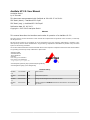
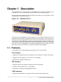
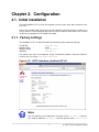
AnaGate UP 2.0
User Manual
Analytica GmbH
A. Schmidt, Analytica GmbH
AnaGate UP 2.0: User Manual
Analytica GmbH
by A. Schmidt
This document was generated with DocBook at 2014-06-17 14:30:01.
PDF-Datei (dtsch.): AnaGateUP2-2.0.pdf
PDF-Datei (engl.): AnaGateUP2-2.0-EN.pdf
Publication date 26. Juli 2013
Copyright © 2007-2013 Analytica GmbH
Abstract
This manual describes the interfaces and modes of operation of a AnaGate UP 2.0.
All rights reserved. All the information in this manual was compiled with the greatest of care. However, no warranty
can be given for it.
No parts of this manual or the program are to be reproduced in any way (printing, photocopying, microfilm or any
other process) without written authorisation. Any processing, duplication or distribution by means of any electronic
system is also strictly prohibited.
You are also advised that all the names and brand names of the respective companies mentioned in this documentation
are generally protected by brand, trademark or patent laws.
Analytica GmbH
Vorholzstraße 36
76137 Karlsruhe
Germany
Fon +49 (0) 721-43035-0
Fax +49 (0) 721-43035-20
<[email protected]>
www.analytica-gmbh.de [http://www.analytica-gmbh.de]
www.anagate.de [http://www.anagate.de]
Revision History
Revision
0.9
10.12.2008
Uwe
Initial version
Revision
1.0
30.09.2009
Uwe
JTAG/Renesas/Power
Revision
1.1
22.07.2010
THa
Change of PIN assignment of Renesas module
Revision
2.0
22.07.2013
ASc
Manual changed to DocBook format and extended to new AnaGate UP
2.0 device.
Table of Contents
Introduction ............................................................................................ vi
1. Description ........................................................................................... 1
1.1. Features ..................................................................................... 1
1.2. Specification ................................................................................ 2
1.3. Scope of delivery ......................................................................... 3
1.4. Interfaces and plugs ..................................................................... 3
2. Configuration ........................................................................................ 7
2.1. Initial installation ......................................................................... 7
2.2. Network settings .......................................................................... 8
2.3. Digital IO .................................................................................... 9
2.4. Factory reset ............................................................................... 9
2.5. Firmware update ........................................................................ 10
3. Fields of application ............................................................................. 13
3.1. Using the SPI interface ............................................................... 13
3.2. Using the I2C interface ............................................................... 13
3.3. Using the JTAG interface ............................................................. 14
3.4. Power interface .......................................................................... 15
A. FAQ - Frequently asked questions .......................................................... 16
B. I2C device list .................................................................................... 20
C. SPI device list ..................................................................................... 21
D. Feature list programming devices .......................................................... 22
E. Programming speed ............................................................................. 24
F. Technical support ................................................................................. 26
Abbreviations .......................................................................................... 27
Bibliography ........................................................................................... 28
iii
© 2007-2013 Analytica GmbH
List of Figures
1.1.
1.2.
1.3.
2.1.
2.2.
2.3.
2.4.
2.5.
2.6.
3.1.
3.2.
3.3.
AnaGate UP 2.0 ................................................................................. 1
Front view, AnaGate UP 2.0 ................................................................. 3
AnaGate UP 2.0, back panel ................................................................ 6
HTTP interface, AnaGate UP 2.0 ........................................................... 7
HTTP interface, network settings .......................................................... 8
Pin layout, digital IO plug .................................................................... 9
AnaGate UP 2.0, Example blinking output ............................................ 10
HTTP interface, AnaGate UP 2.0 .......................................................... 11
HTTP interface, firmware update ......................................................... 11
Universal Programmer connected a single SIP device ............................. 13
Universal Programmer connected to two I2C devices .............................. 14
Universal Programmer connected a JTAG device .................................... 15
iv
© 2007-2013 Analytica GmbH
List of Tables
1.1.
1.2.
1.3.
1.4.
1.5.
A.1.
B.1.
C.1.
D.1.
D.2.
E.1.
E.2.
Technical data, AnaGate UP2 ................................................................ 2
Pin layout, SPI socket ......................................................................... 4
Pin layout, JTAG socket ....................................................................... 4
Pin layout, I2C socket ......................................................................... 5
Pin layout, VAUX socket ...................................................................... 5
Using AnaGate hardware with firewall .................................................. 17
I2C device list .................................................................................. 20
SPI device list .................................................................................. 21
Feature list of universal programming devices ...................................... 22
Feature list of standalone and universal programming devices ................. 22
Programming speed for I2C ............................................................... 24
Programming speed for SPI ................................................................ 24
v
© 2007-2013 Analytica GmbH
Introduction
This document describes the features and objectives of the programming unit
AnaGate UP 2.0.
The AnaGate UP 2.0 is designed to program I2C EEPROMs, SPI EEPROMs and
SPI flash devices. In addition it is also possible to access JTAG-able flash devices
(NOR/NAND/CPUs) via the existing JTAG interface, even the debugging of CPU's is
supported via OpenOCD.
This unit is an improvement of the established AnaGate Universal Programmer
UPP, which provides the core functionality of the ethernet gateways AnaGate I2C
and AnaGate SPI. The concept of transparent access to I2C and SPI bus via
ethernet interface was taken and both hardware interfaces are combined in a single
programing unit. Via the software interface of the AnaGate UP 2.0 any I2C and
SPI commands can be issued. An JTAG interface and a galvanically isolated power
interface for supplying the connected devices or printed circuit boards completes the
unit to a highly flexible programming solution.
A programming software, which can be run in batch mode, for programming of
memory devices is included. Not already supported devices can be added into the
programming software on demand. Alternatively is is also possible to access the
AnaGate UP 2.0 via a free application library (API) and to integrate the unit into
individual software applications.
The AnaGate UP 2.0 is particularly suitable for in series (line) production and insystem programming of pcb's due its reliability and high programming speed. Of
course it is pretty often used in laboratory during development, too.
The connection to the programming unit is always done via a standard network line
(TCP/IP, LAN, WLAN). Installation of additional unit drivers is not neccessary if the
network is already running.
vi
© 2007-2013 Analytica GmbH
Chapter 1. Description
The AnaGate UP 2.0 connects a PC, an embedded PC or an other general device to
a SPI bus, I2C bus or JTAG capable device via the TCP/IP network protocol.
For this reason the AnaGate UP 2.0 provides a SPI interface, an I2C interface, a JTAG
interface and an ethernet interface.
Figure 1.1. AnaGate UP 2.0
Controlling and configuration of an AnaGate UP 2.0 is made through TCP/IP. The
application protocol itself is described in detail (see [TCP-2010]). Thus the access to
the device can be programmed via native calls to the TCP/IP socket interface. This
means that any communication partner with a LAN interface is able to communicate
to the device. Accessing the device with the supplied application libraries for Windows
and Linux is much comfortable. The libraries includes the entire range of device
functions and can be used with conventional programming languages.
1.1. Features
The AnaGate UP 2.0 offers basically interfaces for I2C, SPI and JTAG.
I2C interface
• Supports I2C Read and Write commands for all I2C devices (7 and 10 Bit format).
• Variable I2C bus speed (50, 100, 200, 400, 1000 kbps).
• Galvanically isolated SCL/SDA lines.
SPI interface
• Supports all SPI-Salve devices (sending and receiving data).
• Variable SPI bus speed (200 – 10000 kbps).
• Galvanically isolated CLK/MISO/MOSI/CS lines.
JTAG interface
• Supports JTAG interface to programm flash memories and debug CPUs.
1
© 2007-2013 Analytica GmbH
Description
• Variable JTAG bus speed (10 – 8333 kbps).
• galvanically isolated –TRST, -SRST, TDI, TMD, TCK, TDO lines.
Other features
• Two different plugs for voltage supply.
• Power inteface with output voltage of 1.8V, 2.7V, 3.3V or 5.0V DC
• System is addressed using a proprietary network protocol.
• Static or dynamic assignment (DHCP) of IP address.
• 4 digital inputs and outputs, which can be accessed via LAN/Ethernet.
1.2. Specification
Table 1.1. Technical data, AnaGate UP2
Technical aspect
Measurements
I2C bus
Specfication
Desktop casing
155mm x 105mm x 40mm , fixable on DIN
rail with optional adapter kit
Weight
approx. 315g
Baud rate
Standard Mode (100kbps),
(400kbps), Fast Mode Plus
software configuration
Operating mode
Single Master, Multi Master
Fast Mode
(1000kbps),
High-level SCL/SCA 3,0V - Max: 5,0V (isolated)
SPI bus
JTAG
Digital IO
LAN interface
Interface
6 pole plug with SCL, SCA, Vcc, GND
Baud rate
200 – 10000kbps, software configuration
Operating mode
SPI Master
High-level
Min: 1,8V - Max: 5,5V (isolated)
Interface
10 pole plug with MISO, MOSI, CLK, -SS,
GND, Vcc, GND
Baud rate
10 – 8333kbps, software configuration
Operating mode
JTAG Master Mode
High-level
Min: 1,8V - Max: 5,5V (isolated)
Interface
20 pole plug with –TRST, -SRST, TDI, TMD,
TCK, TDO, Vcc, GND
Inputs
4, galvanically isolated, 3,3 – 24V
Outputs
4, galvanically isolated, 3,3 – 24V (Itotal
= 0,5A)
Baud rate
10/100 Mbps
TCP/IP
Static or dynamic (DHCP) IP address
Interface
RJ45 socket
2
max
© 2007-2013 Analytica GmbH
Description
Technical aspect
Voltage supply
Specfication
Voltage
9V-28V direct current
Power consumption max. 350 mA (9V) without plugged USB
consumers
Ambient
temperature
Storage
0 .. 85 °C
In operation
0 .. 60 °C
1.3. Scope of delivery
The AnaGate UP 2.0 is supplied with the following components:
• 1x AnaGate UP 2.0
• 1x CD with manual, programming API for Windows/Linux, Programming software
for I2C, SPI and JTAG (Windows/Linux)
• 1x 1,8 m Cat. 5 LAN cable (standard, not crossed)
• 1x 10 pole plug connector (for digital IO)
• 1x 2 pole plug connector (for external power supply)
• 1 x plug-in power supply unit, compatible with country of delivery: EU, US or UK.
1.4. Interfaces and plugs
1.4.1. AnaGate UP 2.0 - front view
Figure 1.2. Front view, AnaGate UP 2.0
The front panel of the AnaGate UP 2.0 features the following connectors (from left
to right):
SPI port
10 pole connector plug to connect the SPI bus (galvanically isolated).
The pin allocation of the plug can be inferred from the following table.
3
© 2007-2013 Analytica GmbH
Description
Table 1.2. Pin layout, SPI socket
Pin
Type
VccIN
External voltage for
SPI (1.8 up to 5V
DC)
CLK
Output
Clock line
-SS
Output
Slave Select
(low active)
MOSI
Input
MISO
Output
GND
JTAG port
Description
line
Master-In
Out
Slave-
Master-Out
In
Save-
Ground
20 pole connector plug to connect the SPI bus (galvanically isolated).
The pin allocation of the plug can be inferred from the following table.
Table 1.3. Pin layout, JTAG socket
Pin
Type
VccIN
External voltage for
JTAG (1.8 up to 5V
DC)
-TRST
Output
TDI
Input
Test Data Input
TMS
Input
Test Mode Select
Input
TCK
Output
Test Clock
TDO
Output
Test Data Output
-SRST
Output
Slave Reset
GND
NC
I2C port
Description
Test Reset
Ground for JTAG
not connected
6 pole connector plug to connect the I2C bus (galvanically isolated).
The pin allocation of the plug can be inferred from the following table.
4
© 2007-2013 Analytica GmbH
Description
Table 1.4. Pin layout, I2C socket
Pin
Type
VccIN
External voltage for I2C
(1.8 up to 5V DC)
SCL
Input/
Output
Clock line for I2C
SDA
Input/
Output
Data line for I2C
GND
VAUX port
Description
Ground for I2C
10 pole connector plug to power supply the connected PCB's.
The pin allocation of the plug can be inferred from the following table.
Table 1.5. Pin layout, VAUX socket
Pin
Type
Description
5VOUT
Output
5V output for current
supply of devices up to
200mA
3,3VOUT
Output
3.3V output for current
supply of devices up to
200mA
2,7VOUT
Output
2.7V output for current
supply of devices up to
200mA
1,8VOUT
Output
1.8V output for current
supply of devices up to
200mA
GND
Ground for SPI
NC
not connected
5
© 2007-2013 Analytica GmbH
Description
1.4.2. AnaGate UP 2.0 rear view
Figure 1.3. AnaGate UP 2.0, back panel
The rear panel of the AnaGate UP 2.0 features the following connectors and LEDs
(from left to right):
Power LED
This green LED lights up when voltage is being supplied.
Power supply
The AnaGate UP 2.0 can be power supplied in two different ways.
For the use as desktop device the barrel connector socket is
intended, in order to supply the device via a plug power supply
For the use in a switchboard the two-pole Wago clamping socket can
be used to connect an external power supply.
Warning
Be sure to use only one power supply.
LAN
Via the RJ45 socket the AnaGate UP 2.0 is connected with the
Ethernet. The device can be connected to a network component like
a hub or a switch. For a direct connection to a PC a crossover network
cable has to be used.
USB Hosts
The AnaGate UP 2.0 has two USB 1.1 interfaces for further
extensions or customer specific solutions.
Digital IO
The AnaGate UP 2.0 has 4 digital inputs and 4 digital outputs which
can be used freely. The digital io are galvanically decoupled from
the device and must be externally power supplied from 3,3V to 24V
(see Section 2.3, “ Digital IO”).
Reset
The AnaGate UP 2.0 can be reset to the factory settings using this
button (see Section 2.4, “ Factory reset” for further details).
Activity LED
This yellow LED lights up when the AnaGate UP 2.0 is processing
incoming CAN messages.
6
© 2007-2013 Analytica GmbH
Chapter 2. Configuration
2.1. Initial installation
First the AnaGate UP 2.0 must be supplied via the power plug with a tension from
9 to 24 V.
Insert the included LAN cable into the plug labelled LAN and connect it either to a
hub or switch. If connecting directly to a PC use a crossover LAN cable (not in scope
of delivery) instead of the included LAN cable.
2.1.1. Factory settings
The AnaGate UP 2.0 is delivered with the following initial network settings:
IP address
Address type
Network mask
Gateway
192.168.1.254
static
255.255.255.0
192.168.1.1
The device can now be configured using a standard browser (Internet Explorer,
Firefox, etc.) by using http://192.168.1.254 .
Figure 2.1. HTTP interface, AnaGate UP 2.0
Note
The PC used for the configuration must be in the 192.168.1.x network.
The static IP address 192.168.1.2 with the subnet mask 255.255.255.0
7
© 2007-2013 Analytica GmbH
Configuration
can be e.g. used. If neccessary the settings of the network interface on
the configuration pc has to be changed temporarily.
2.2. Network settings
On the page IP Settings the following settings can be changed.
DHCP
Here you can switch between static IP and dynamic (via DHCP)
addresses. If DHCP is being used, the remaining fields are ignored,
because this information is retrieved from the DHCP server.
In this case, a DHCP server must be available and accessible in the
network.
IP address
The IP address of the AnaGate UP 2.0 is entered in dot format (e.g.
192.168.1.200).
Subnet mask
The subnet mask is entered in dot format (e.g. 255.255.255.0).
Gateway
The default gateway is entered in dot format (e.g. 192.168.1.1).
Leave blank or enter 0.0.0.0 if a default gateway is not required.
Figure 2.2. HTTP interface, network settings
The inputs will be taken over immediately after clicking the button Save settings
and saved permanently on the AnaGate UP 2.0. A restart of the device is not
necessary for activation of the settings.
Note
Maybe the ARP cache of the PC has to be deleted to find the device with
the changed IP address.
8
© 2007-2013 Analytica GmbH
Configuration
2.3. Digital IO
2.3.1. Pin layout of plug
Over the 10-pole pin row on the back of the AnaGate UP 2.0four digital inputs and four
digital outputs are led out, which can be used freely. Since the IO's are electrically
isolated from the device, they must be separately supplied via the pins 1 us 2 with
a voltage by 3,3V - 24V DC.
Figure 2.3. Pin layout, digital IO plug
2.3.1.1. Connecting the digital inputs
At the inputs IN1 to IN4 any external voltage between VCC and GND can be applied.
As soon as the voltage difference between INx and GND is more than 1.0 V, the
AnaGate UP 2.0 interprets the input as logically HI otherwise LOW.
2.3.1.2. Connecting the digital outputs
The outputs are implemented as open collector drivers. If a output is active, it is
pulled down to GND. In the inactive condition the output is floating.
In principle the maximum current of each individual output is 400mA. For thermal
reasons is the sum of all output currents is limited to 500mA. The outputs not shortcircuit proofed, and must be protected with a pre-resistor.
Warning
The outputs are not short-circuit-safe!
2.4. Factory reset
In order to restore the default factory settings, hold the RESET for approx. 10
seconds. If the device is reset successfully, the yellow LED blinks until the RESET
is released.
The default factory settings are activated immediately without a restart of the device:
IP address
Address type
192.168.1.254
static
9
© 2007-2013 Analytica GmbH
Configuration
Network mask
Gateway
255.255.255.0
192.168.1.1
Important
If the RESET push-button is pressed too briefly, the actual IP address and
network mask is pulsed via the yellow LED (Morse code). A second push
of the RESET terminates the pulsing, the device is not reset.
Note
The factory reset is not possible directly after power on until complete
loading of the operating system and the firmware of the device. This
initialization period is signalled via the yellow activity LED. On power on
the LED is switched on and after initialization the LED is switched off.
Note
Maybe the ARP cache of the PC has to be deleted to find the device with
the changed IP address.
2.4.1. Examining the network settings
It is possible to check the current network settings directly on the device.
After pressing shortly the RESET button the device starts to pulse out the current
n settings via the yellow activity LED. Pressing again the buttons stops the pulsing
immediately.
The IP address and subnet mask are pulsed out, one after the other. Following pulse
codes are used:
• Digits 1, 2, 3, ...., 9: 1x, 2x, ...9x Flashing (200ms delay between each flash)
• Digit 0: 10x flashing (200ms delay between each flash)
• Dot: 1x very fast flash
Between two single digits a delay of 1 seconds is made, and between the IP address
and subnet mask two fast flashes are pulsed out.
Figure 2.4. AnaGate UP 2.0, Example blinking output
2.5. Firmware update
The device firmware of the AnaGate UP 2.0 is updated via the integrated web server
of the device.
10
© 2007-2013 Analytica GmbH
Configuration
On the home page of the web server the current firmware information is displayed.
Figure 2.5. HTTP interface, AnaGate UP 2.0
Proceed please as follows, in order to install the firmware on the AnaGate UP 2.0:
• Click Firmware on the left navigation bar to navigate to the Firmware-Upload page.
Figure 2.6. HTTP interface, firmware update
• Select the update package (file extension *.upd) via the Browse button.
• Clicking on the button Upload loads the update file to the device and starts the
update process.
11
© 2007-2013 Analytica GmbH
Configuration
• During the update process several installation messaged are displayed on the
website. If the update is successfully finished, Update done! is displayed.
When the update is finished the browser navigates back to the home page. Check,
if the new firmware version is display here.
Warning
If the firmware could not be flashed correctly on the device, the AnaGate
may not longer ready for operation.
Please visit our web site http://www.anagate.de for further information.
12
© 2007-2013 Analytica GmbH
Chapter 3. Fields of application
3.1. Using the SPI interface
Before using the SPI interface the Vcc and GND pins have to be supplied with an
external voltage of 1.8V up to 5.0V DC. The signal level of the interface is always
identical to the supply voltage. So, it is advisable to supply the interface and the
device to program with the same power supply. Since the interface is galvanically
isolated, the supply voltage of the programming board can be used for example. On
the AnaGate UP 2.0 and on the AnaGate UPP the installed power module can be used
to supply the SPI device (up to 200mA) directly .
When using higher baud rates, ensure that a GND is present between two signal
lines. The cables should be kept as short as possible.
In the following picture the use of the I2C interface is schematically shown.
Figure 3.1.
device
Universal Programmer connected a single SIP
The lines have to be interconnected as follows:
MOSI This line have to be interconnected to the data input of the SPI Slave (often
referred as DI or SI).
MISO This line have to be interconnected to the data output of the SPI Slave (often
referred as DO or SO).
CLK
This line have to be interconnected to the clock input of the SPI Slave (often
referred as CLK or SCK).
-SS
This line have to be interconnected to the chip select input of the SPI Slave
(often referred as -SS or -CS).
3.2. Using the I2C interface
Before using the I2C interface the Vcc and GND pins have to be supplied with an
external voltage of 3.3V up to 5.0V DC. The signal level of the interface is always
13
© 2007-2013 Analytica GmbH
Fields of application
identical to the supply voltage. Since the interface is galvanically isolated, the supply
voltage of the programming board can be used. On the AnaGate UP 2.0 and on the
AnaGate UPP the installed power module can be used to supply the I2C device (up
to 200mA) directly .
Two 4.7 kOhm pull-up resistors have to be switched between the voltage supply and
the SDA or SCL circuit. These are not integrated in the Anagate UP 2.0 and must be
attached externally. In most cases these resistors are already present on the boards
to program.
In the following picture the use of the I2C interface is schematically shown.
Figure 3.2.
devices
Universal Programmer connected to two I2C
If the I2C device is fitted with chip-enable address inputs (usually designated A0/
E0, A1/E1 and A2/E2), these also have to be provided with GND or power.
3.3. Using the JTAG interface
Before using the SPI interface the Vcc and GND pins have to be supplied with an
external voltage of 1.8V up to 5.0V DC. The signal level of the interface is always
identical to the supply voltage. So, it is advisable to supply the interface and the
device to program with the same power supply. Since the interface is galvanically
isolated, the supply voltage of the programming board can be used for example. On
the AnaGate UP 2.0 and on the AnaGate UPP the installed power module can be used
to supply the JTAG device (up to 200mA) directly .
When using higher baud rates, ensure that a GND is present between two signal
lines. The cables should be kept as short as possible.
In the following picture the use of the JTAG interface is schematically shown.
14
© 2007-2013 Analytica GmbH
Fields of application
Figure 3.3. Universal Programmer connected a JTAG device
The lines have to be interconnected as follows:
TMS,
TCK
These lines have to be interconnected to each JTAG device to the same
designation.
TRST,
SRST
These lines have to be interconnected to each JTAG device to the same
designation. The connection is optional (test and system reset lines).
TDI
This line have to be interconnected to the TDI (data input) of the JTAG
device.
TDO
This line have to be interconnected to the TDO of the JTAG device in single
device mode.
If there is more than a single JTAG device is attached, the TDO of the first
device is interconnected to the TDO of the second, and so one. The TDO of
the last JTAG device have to be interconnected to the TDO of the AnaGate
Universal Programmer.
Note
RCLK is not supported by the AnaGate Universal Programmer.
3.4. Power interface
The power interface VAUX make the following voltages available during a maximum
total current load of 200mA:
• 1.8V DC
• 2.7V DC
• 3.3V DC
• 5.0V DC
These tensions can be used, to supply a PCB during programming.
15
© 2007-2013 Analytica GmbH
Appendix A. FAQ - Frequently asked
questions
Here is a list of frequently asked questions.
A.1. Common questions
Q:
No network connection (1)
A:
Please check the physical connection to the device first. In general the AnaGate
has to be connected directly to a personal computer or to an active network
component (hub, switch). If the AnaGate device is connected to a personal
computer a cross-wired network cable must be used to connect the device,
otherwise the included network cable is to be used.
The physical interconnection is OK if the yellow link LED turns on when LAN
cable is plugged in. The yellow light stays on until the connection breaks down.
On some hardware models the link LED flickers synchronously to the green
activity LED if there is traffic on the network line.
If the link LED is always off then please check the wiring between the AnaGate
and the hub, switch or the personal computer.
Q:
No network connection (2)
A:
If the link LED indicates a proper Ethernet connection (see previous FAQ) but
you still can't connect to the AnaGate then please try the following:
1.
Check if the AnaGate can be reached via ping. To do so in Windows, open
a command prompt and enter the command ping a.b.c.d, where a.b.c.d
is the device IP address.
2.
In case the AnaGate is unreachable via ping, reset the device to factory
settings. Set the IP address of your PC to 192.168.1.253 and the subnet
mask to 255.255.255.0. Check if the AnaGate can be reached via ping
192.168.1.254.
3.
If the device can be reached via ping then the next step is to try if you can
open a TCP connection to port 5001. Open a Windows command prompt
and enter telnet a.b.c.d 5001, where a.b.c.d is the device IP address. If
this command fails check if a firewall runs on your PC or if there is a packet
filter in the network between your PC and the AnaGate.
16
© 2007-2013 Analytica GmbH
FAQ - Frequently
asked questions
Q:
No network connection after changing the network address
A:
After changing the network address of the AnaGate device via web interface
the device is not longer reachable. The used internet browser displays only an
empty web page, additional error messages are not available.
Please check if your anti-virus software has blocked the new network address.
After changing the network address you are redirected to the new network
address in the browser. Such activity is suspicious for some anti-virus software
so they block the new web page, sometimes even without notification of the
user.
Q:
Connection problems using multiple devices
A:
If multiple devices with identical IP addresses are used in a local area network
at the same time the connections to the devices are not stable. Because of this
behaviour it is necessary to use different IP addresses.
This problem can also occur if devices with identical IP addresses are used not
concurrently but within short intervals. For example this can arise if some new
devices which have the default IP address 192.168.1.254 are configured from
a single PC.
The Address Resolution Protocol (ARP) is used in IPv4 networks to
determine the MAC address of a given IP address. The necessary information
is cached in the ARP table. If there is a wrong entry in the ARP table or even
an entry which is not up-to-date it is not possible to communicate with the
corresponding host.
An entry in the ARP table is deleted if it is not used any more after a short period
time. The time interval used depends on the operating system. On a current
Linux distribution an unused entry is discarded after about 5 minutes. The ARP
cache can be displayed and manipulated with the arp on Windows and Linux.
C:\>arp -a
Schnittstelle: 10.1.2.50 --- 0x2
Internetadresse
Physikal. Adresse
192.168.1.254
00-50-c2-3c-b0-df
Typ
dynamisch
The command arp -d can be used to empty the ARP Cache.
Note
Possibly the ARP cache of the PC has to be deleted if the IP address
of a device is changed.
Q:
Using a firewall
A:
When working with a firewall a TCP port has to be opened for communication
with the AnaGate device:
Table A.1. Using AnaGate hardware with firewall
Device
Port number
AnaGate I2C
5000
17
© 2007-2013 Analytica GmbH
FAQ - Frequently
asked questions
Device
Port number
AnaGate I2C X7
5100, 5200, 5300,
5500, 5600, 5700
AnaGate CAN
5001
AnaGate CAN USB
5001
AnaGate CAN uno
5001
AnaGate CAN duo
5001, 5101
AnaGate CAN quattro
5001, 5101, 5201, 5301
AnaGate CAN X1
5001
AnaGate CAN X2, AnaGate CAN-FD X2
5001, 5101
AnaGate CAN X4, AnaGate CAN-FD X4
5001, 5101, 5201, 5301
AnaGate CAN X8
5001, 5101, 5201, 5301,
5401, 5501, 5601, 5701
AnaGate SPI
5002
AnaGate Renesas
5008
AnaGate Universal Programmer UP/UPP
5000, 5002, 3333, 4444, 20,
21
AnaGate Universal Programmer UPR
5000, 5002,
4444, 20, 21
AnaGate Universal Programmer UP 2.0
5000, 5002, 3333, 4444, 20,
21
5008,
5400,
3333,
A.2. Questions concerning the SPI interface
Q:
No SPI communication
A:
If SPI communication with your SPI device fails, please proceed as follows:
1.
Check that the SPI device and the SPI interface of the AnaGate UP 2.0 are
connected to a power supply.
2.
Check that no other devices/μC are active on the SPI bus.
3.
Ensure that no other electrical components can interfere with
communication on the SPI bus between the AnaGate Universal Programmer
and the SPI device.
A.3. Questions concerning the I2C interface
Q:
No I2C communication
A:
If I2C communication with your I2C device fails, please proceed as follows:
1.
Check that the I2C device and the I2C interface of the AnaGate UP 2.0 are
connected to a power supply.
2.
Check that no other devices/μC are active on the I2C bus.
3.
Ensure that the SDA and SCL circuits are provided with an adequate pullup resistance (e.g. 4.7 kOhm) to the voltage supply (3.3 V resp. 5 V).
18
© 2007-2013 Analytica GmbH
FAQ - Frequently
asked questions
4.
Ensure that no other electrical components can interfere with
communication on the I2C bus between the AnaGate I2C and the I2C
device.
5.
Ensure that the chip-enable address of the I2C device and the software are
identical.
Q:
What is the correct order to connect the GND, SCL and SDA when using an
external power supply?
A:
To avoid potential damage to the AnaGate UP 2.0 the GND pin MUST be
connected to the application board first. Only then can the SCL and SDA pins
be allowed to make contact with the application board.
A.4. Questions concerning the JTAG interface
Q:
No JTAG communication
A:
If JTAG communication with your JTAG device fails, please proceed as follows:
1.
Check that the JTAG device and the JTAG interface of the AnaGate UP 2.0
are connected to a power supply.
2.
Ensure that the TDO pin of the last JTAG device is connected to the TDO
pin of the AnaGate UP 2.0.
19
© 2007-2013 Analytica GmbH
Appendix B. I2C device list
The AnaGate UP 2.0 provides with its I2C inferface a fully working I2C-Ethernet
gateway, which can perform Read/Write requests from the PC via ethnernet to a
connected I2C bus. Accesing serial I2C EEPROMs is included in particular.
The free programming software I2C EEPROM Programmer uses this feature and
extends the AnaGate UP 2.0 to a remarkably efficient programming tool for I2C
EEPROM devices.
As an example the supported different EEPROM devices of a single manufacturer
are listed in the following table. Of course, all identical hardware devices of other
manufacturers are supported too.
Table B.1. I2C device list
Part-No.
Mamufacturer
Memory
M24C01, M24LC01
STMicroelectronics
1 Kbit
M24C02, M24LC01
STMicroelectronics
2 Kbit
M24C04, M24LC04
STMicroelectronics
4 Kbit
M24C08, M24LC08
STMicroelectronics
8 Kbit
M24C16, M24LC16
STMicroelectronics
16 Kbit
M24C32, M24LC32
STMicroelectronics
32 Kbit
M24C64, M24LC64
STMicroelectronics
64 Kbit
M24C128, M24LC128
STMicroelectronics
128 Kbit
M24C256, M24LC256
STMicroelectronics
256 Kbit
M24C512, M24LC512
STMicroelectronics
512 Kbit
M24M01
STMicroelectronics
1024 Kbit
M24M02
STMicroelectronics
2048 Kbit
Important
If a I2C device does not still exist in the device databare of the software
I2C EEPROM Programmer, it can be added permanently. The required
settings can be found in the device data sheet,
20
© 2007-2013 Analytica GmbH
Appendix C. SPI device list
The AnaGate UP 2.0 provides with its SPI inferface a fully working SPI-Ethernet
gateway, which can perform data requests from the PC via ethnernet to a connected
SPI bus. Accesing serial SPI EEPROM and other memory devices is included in
particular.
The free programming software SPI EEPROM Programmer uses this feature and
extends the AnaGate UP 2.0 to a remarkably efficient programming tool for SPI
EEPROM and other memeory devices.
As an example some supported devices of a different manufacturer are listed in the
following table. Of course, all identical hardware devices of other manufacturers are
supported too.
Table C.1. SPI device list
Part-No.
Manufacturer
Algorithm
M95128, M95256, M95640
ST
M25P05, M25P10, M25P20, M25P30, M25P40,
M25P80, M25P128, M25PX30
ST
FM25CL64S
Ramtron
ST
AT25010A, AT25020A, AT25040A, AT25128,
AT25160A, AT25256, AT2532A, AT25640A
AT250x0A
AT25F512, AT25F2048, AT25F4096
AT25Fxxx
AT24BD041D,
AT24BD081D,
AT24BD161D,
AT24BD321D, AT24BD641D, AT24BD642D
AT45xxx
Important
If a I2C device does not still exist in the device databare of the software
SPI EEPROM Programmer, Analytica can check if the missing device is
currently supported. The required informations are mostly found in the
device data sheet. Adding new programming algorithm in the SPI EEPROM
Programmer is possible on demand.
21
© 2007-2013 Analytica GmbH
Appendix D. Feature list programming
devices
Table D.1. Feature list of universal programming devices
Feature
System
I2C Bus
Universal Programmer
AnaGate
UPP
AnaGate
UPR
Universal
Programmer 2.0
Hardware
AnaGate
UP
AnaGate UP 2.0
Processor
ARM9 (32bit, 200MHz)
ARM9
200MHz)
Baud rates
50, 100, 200, 400 kpbs
50, 100, 200, 400,
1000 kpbs
(32bit,
Operatinf modes Single Master
Single, Multi Master
SPI Bus
Baud rates
200 to 8333 kpbs
200 to 10000 kpbs
JTAG
Baud rates
10 to 8000 kpbs
10 to 8000 kpbs
Renesas
Baud rates
Power
Output voltage
Digital IO Inputs
Outputs
9600,
19200,
38400,
57600
kpbs
1.8V,
2.7V,
3.3V,
5.0V
4
4
4
4
Table D.2.
Feature
programming devices
Feature
System
I2C Bus
1.8V,
5.0V
list
of
I2C
Programmer
2.7V,
3.3V,
standalone
and
SPI
Programmer
Universal
Programmer 2.0
AnaGate SPI
universal
Hardware
AnaGate I2C
AnaGate UP 2.0
Processor
eZ80 Acclaim(8bit)
ARM9 (32bit)
Operating
System
Zilog ZTP (RTOS)
Linux (Kernel 2.6.20)
USB
2 x USB 1.1
Indiv.
extensions
upload of executables
(GCC)
Temp. range
0 -60°C
0 -60°C
0 -60°C
Input voltage
8 .. 28V DC
8 .. 28V DC
8 .. 28V DC
Baud rates
50, 100, 200,
400 kpbs
22
50, 100, 200, 400,
1000 kpbs
© 2007-2013 Analytica GmbH
Feature list
programming devices
Feature
Operatinf
modes
I2C
Programmer
SPI
Programmer
Single Master
Universal
Programmer 2.0
Single, Multi Master
SPI Bus
Baud rates
JTAG
Baud rates
10 to 8000 kpbs
Power
Output voltage
1.8V, 2.7V, 3.3V, 5.0V
LAN
Speed
Digital IO Inputs
Outputs
10 to 8600 kpbs 200 to 10000 kpbs
10/100 Mbps
10/100 Mbps
4
4
4
4
4
4
23
© 2007-2013 Analytica GmbH
Appendix E. Programming speed
The specific behavior of the Universal Programmer compared to the predecessor
models for SPI and I2C is shown in the following tables on the basis of two different
reference devices.
Table E.1. Programming speed for I2C
Programmer
Device
Size
AnaGate I2C
AT24C1024
128KB
400
kbps
6.4s
5.1s
11.5s
AnaGate UP
AT24C1024
128KB
400
kbps
5.0s
3.8s
8.8s
AnaGate UP 2.0
AT24C1024
128KB
400
kbps
4.6s
3.8s
8.4s
AnaGate UP 2.0
AT24C1024
128KB
1 Mbps
2.6s
2.1s
4.7s
64KB
400
kbps
3.8s
2.0s
5.8s
AnaGate UP 2.0
1
24LC512
1
Baud
rate
Program Verify
Total
max. 400 kBit/s
Table E.2. Programming speed for SPI
Programmer
Device
Size
Baud
rate
Delete Program Verify
Total
AnaGate SPI
AT45DB642D 4MB
6,25
MHz
18.2s 123.0s
61.9s 202.9s
AnaGate UP
AT45DB642D 4MB
6,25
MHz
18.1s
56.1s
31.9s 106.2s
AnaGate UP
AT45DB642D 4MB
8.33
MHz
18.1s
56.0s
31.8s 105.9s
AnaGate UP 2.0 AT45DB642D 4MB
8.33
MHz
18.1s
20.6s
21.0s
59.7 s
AnaGate UP 2.0 AT45DB642D 4MB
10.0
MHz
18.1s
19.4s
19.6s
57.1s
AnaGate SPI
M25P16
2MB
6,25
MHz
14.8s 141.6s
AnaGate UP
M25P16
2MB
8,33
MHz
14.7s
37.8s
8.0s
60.5s
AnaGate UP 2.0 M25P16
2MB
10,0
MHz
14.7s
9.9s
5.0s
29.6s
28.7s 185.1s
Note
A conventional PC (Intel Core2 Duo E8400, 3.0 GHz, 4 GB RAM
running Windows 7 64bit SP1) was used for taking the readings. everal
measurements are taken and averaged, the memory was always written
24
© 2007-2013 Analytica GmbH
Programming speed
and read completely from and to the personal computer by use of the
LAN interconnection
25
© 2007-2013 Analytica GmbH
Appendix F. Technical support
The AnaGate hardware series, software tools and all existing programming interfaces
are developed and supported by Analytica GmbH. Technical support can be requested
as follows:
Internet
The AnaGate web site [http://www.anagate.de/en/index.html] of Analytica GmbH
contains information and software downloads for AnaGate Library users:
• Product updates featuring bug fixes or new features are available here free of
charge.
E-Mail
If you require technical assistance over the Internet please send an e-mail to
<[email protected]>
To help us provide you with the best possible support please keep the following
information and details at hand when you contact our support team.
• Version number of the used programming tool or AnaGate library
• AnaGate hardware series model and firmware version
• Name and version of the operating system you are using
26
© 2007-2013 Analytica GmbH
Abbreviations
I2C
Inter-Integrated Circuit
SCL
Serial Clock Line
SDA
Serial DAta Line
SPI
Serial Peripheral Interface
CLK
Clock
MISO
Master In Slave Out
SS
Slave Select
MOSI
Master Out Slave In
TRST
Test Reset
SRST
Slave Reset
JTAG
Joint Test Action Group
TDI
Test Data Input
TDO
Test Data Output
TMS
Test Mode Select Input
TCK
Test Clock
DHCP
Dynamic Host Configuration Protocol
27
© 2007-2013 Analytica GmbH
Bibliography
Books
[LuaRef2006-EN] Roberto Ierusalimschy, Luiz Henrique Figueiredo, and Waldemar Celes.
Copyright © 2006 R. Ierusalimschy, L. H. de Figueiredo, W. Celes. ISBN 85-903798-3-3.
Lua.org. Lua 5.1 Reference Manual.
[LuaProg2006-EN] Roberto Ierusalimschy. Copyright © 2006 Roberto Ierusalimschy, Rio de
Janeiro. ISBN 85-903798-2-5. Lua.org. Programming in Lua (second edition).
[LuaProg2013-EN] Roberto Ierusalimschy. Copyright © 2013 Roberto Ierusalimschy, Rio de
Janeiro. ISBN 85-903798-5-X. Lua.org. Programming in Lua, Third Edition.
Other publications
[NXP-I2C] NXP Semiconductors. Copyright © 2007 NXP Semiconductors. UM10204. I2C-bus
specification and user manual. Rev. 03. 19.06.2007.
[TCP-2010] Analytica GmbH. Copyright © 2010 Analytica GmbH.
communication . Version 1.2.6. 15.05.2008.
[Prog-2013] Analytica GmbH. Copyright © 2013 Analytica GmbH.
Programmer's Manual . Version 2.0. 15.05.2013.
Manual TCP-IP
AnaGate API 2 .
[CiA-DS301] Copyright © 2002 CAN in Automation (CiA) e. V.. CAN in Automation (CiA) e.V..
13.02.2002. Cia 301, CANopen Application Layer and Communication Profile.
28
© 2007-2013 Analytica GmbH