1
Lark Board
User Manual
Version 1.1 – Aug. 30th, 2014
Embest Technology
i
Copyright Statement:
Lark Board and its related intellectual property are owned by Shenzhen Embest
Technology Co., Ltd.
Shenzhen Embest Technology has the copyright of this document and reserves
all rights. Any part of the document should not be modified, distributed or
duplicated in any approach and form with the written permission issued by
Embest Technology Co., Ltd.
Disclaimer:
Shenzhen Embest Technology does not take warranty of any kind, either
expressed or implied, as to the program source code, software and documents in
the CD/DVD-ROMs provided along with the products, and including, but not
limited to, warranties of fitness for a particular purpose; The entire risk as to the
quality or performance of the program is with the user of products.
FCC NOTICE:
This kit is designed to allow:
(1) Product developers to evaluate electronic components, circuitry, or software
associated with the kit to determine whether to incorporate such items in a finished
product and
(2) Software developers to write software applications for use with the end product.
This kit is not a finished product and when assembled may not be resold or otherwise
marketed unless all required FCC equipment authorizations are first obtained.
Operation is subject to the condition that this product not cause harmful interference
to licensed radio stations and that this product accept harmful interference.. For
evaluation only; not FCC approved for resale
Copyright © 2014 Embest Technology
Lark Board User Manual
Embest Technology
ii
European Union Notice:
This kit is a custom built evaluation kit destined for professionals to be used solely at
research and development facilities for such purposes.
Revision History:
Version
Date
Description
1.0
1.1
2014-6-30
2014-8-30
Original Version
Revision
Copyright © 2014 Embest Technology
Lark Board User Manual
Embest Technology
iii
Table of Contents
Chapter 1
Product Overview ........................................................................................ 1
1.1
Brief Introduction ............................................................................................ 1
1.1.1
Packing List ..................................................................................... 1
1.1.2
Product Features ............................................................................. 2
1.2
System Block Diagram................................................................................... 4
1.3
Product Dimensions(mm) .............................................................................. 5
Chapter 2
Introduction to Hardware System .............................................................. 6
2.1
Overview of CPU ........................................................................................... 6
2.2
Introduction to Peripheral Chips .................................................................... 6
2.2.1
DDR3 ............................................................................................... 6
2.2.2
eMMC Flash .................................................................................. 11
2.2.3
CH7033B ....................................................................................... 11
2.2.4
AR8035.......................................................................................... 11
2.3
I/O Voltages.................................................................................................. 12
2.4
Details of Interfaces ..................................................................................... 12
2.4.1
LCD/VGA/HDMI ............................................................................ 13
2.4.2
SDI ................................................................................................. 18
2.4.3
PCIe ............................................................................................... 18
2.4.4
Camera .......................................................................................... 20
2.4.5
ADC & Pre-Amp ............................................................................ 21
2.4.6
Gigabit Ethernet ............................................................................ 24
2.4.7
eMMC& TF Card ........................................................................... 25
2.4.8
USB PHY & HUB ........................................................................... 27
2.4.9
USB Blaster & JTAG ..................................................................... 28
2.4.10
DIP Switch ..................................................................................... 30
2.4.11
Jumpers ......................................................................................... 33
2.4.12
Buttons .......................................................................................... 33
2.4.13
UART ............................................................................................. 34
2.4.14
LED ................................................................................................ 35
2.4.15
RTC ............................................................................................... 36
2.4.16
Extension Interfaces ...................................................................... 36
Copyright © 2014 Embest Technology
Lark Board User Manual
Embest Technology
iv
Chapter 3
Quick Use of Lark Board ........................................................................... 39
Chapter 4
Linux ............................................................................................................ 44
4.1
Linux System Structure of Lark Board ......................................................... 44
4.2
Software Resources..................................................................................... 44
4.3
Building Development Environment ............................................................ 46
4.4
4.5
4.6
4.7
4.8
4.9
4.3.1
Building Linux Development Environment .................................... 46
4.3.2
Installing Altera SoC Development Software ................................ 47
4.3.3
Installing Linux Cross-Compiler (Optional) ................................... 47
System Compilation ..................................................................................... 47
4.4.1
Compiling U-boot and Preloader ................................................... 48
4.4.2
Compiling Linux Kernel ................................................................. 48
4.4.3
Generating FPGA RBF Configuration File .................................... 49
System Update ............................................................................................ 52
4.5.1
Updating Images in TF Card ......................................................... 52
4.5.2
Updating Images in eMMC Flash .................................................. 56
Introduction to Drivers .................................................................................. 60
4.6.1
MMC/SD Driver ............................................................................. 61
4.6.2
Frame Buffer Driver ....................................................................... 62
4.6.3
ADC Driver .................................................................................... 63
Configuring Display Modes .......................................................................... 65
4.7.1
VGA/HDMI Output ......................................................................... 65
4.7.2
Configuring for 7” LCD .................................................................. 66
4.7.3
Configuring for 4.3” LCD ............................................................... 66
Example Applications ................................................................................... 66
4.8.1
LED Test ........................................................................................ 66
4.8.2
Button (Keypad) Test ..................................................................... 67
4.8.3
PCIe Test ....................................................................................... 68
4.8.4
Network Interface Test................................................................... 69
4.8.5
ADC Test ....................................................................................... 70
4.8.6
CAM8000-D Camera Test ............................................................. 70
Application Development and DS-5 Debugging .......................................... 72
4.9.1
Development of LED Application................................................... 72
Copyright © 2014 Embest Technology
Lark Board User Manual
Embest Technology
v
4.9.2
Development of FFT Application ................................................... 73
4.9.3
DS-5 Debugging ............................................................................ 77
Chapter 5
FPGA ........................................................................................................... 79
5.1
FPGA Resources ......................................................................................... 79
5.2
FPGA Development ..................................................................................... 79
5.3
5.2.1
Building FPGA Project and Programming SOF File into FPGA.... 80
5.2.2
Elipse Debugging .......................................................................... 83
FPGA Function Implementation on Lark Board ........................................... 87
5.3.1
Input of Camera Video .................................................................. 87
5.3.2
Output of Camera Video................................................................ 89
5.3.3
LCD/VGA/HDMI Video Output ...................................................... 92
5.3.4
Input/output of SDI Video .............................................................. 95
5.3.5
Input Data from ADC ..................................................................... 99
5.3.6
PCIe Function .............................................................................. 100
Technical Support and Warranty.................................................................................. 104
Copyright © 2014 Embest Technology
Lark Board User Manual
Embest Technology
1
Chapter 1 Product Overview
1.1 Brief Introduction
Lark Board is an evaluation board designed by Embest based on an Altera ARM
(Cortex-A9 dual-core)+FPGA processor for areas such as medical instruments, video
surveillance and industrial control. The SoC, named 5CSXFC6D6F31 that comes from
Cyclone V SX family, integrates not only the traditional FPGA fabric, but also an ARM
Cortex-A9-based HPS (operating at 800MHz) and a high-speed transceiver (3Gbps
Serdes) hard subsystem.
Lark Board provides 1GB DDR3 SDRAM separately for both ARM and FPGA, and has 4
high-speed USB2.0 Host interfaces, a TF card slot for mass storage, a 12-bit camera
interface, a VGA interface, a 24-bit LCD interface, PCIe, UART, JTAG, 3Gbps SDI
input/output and a HDMI interface. Additionally, two 2*200-pin connectors are mounted on
the board in order to make the unused pins of HPS/FPGA available for users. Lark Board
uses a switching power supply controller chip (integrated with inductor) that comes from
Altera’s Enpirion family to provide a stable and efficient output for each BANK of FPGA.
Meanwhile, it has two on-board DIP switches used to enable various voltage levels
required by the different interfaces on the board with the purpose to facilitate power
consumption evaluation conducted by users.
Lark Board comes with a lot of FPGA example applications and the corresponding source
code, Linux 3.10 and u-boot source code and Debian 7.4 system image, as well as
schematics and key chips’ datasheets to help users implement evaluation and secondary
development fast.
1.1.1
Packing List
Lark Board×1
USB cable for FPGA programming and control×1
Copyright © 2014 Embest Technology
Lark Board User Manual
Embest Technology
19V DC power adapter×1
8GB TF card×1
12V-DC Fan
1.1.2
2
Product Features
General Specifications:
Operating Temperature: 0℃ ~ 70℃
Power Supply: 12~20V
Operating Humidity: 20% ~ 90%
Dimensions: 180mm x 120mm
PCB Layers: 10-layer PCB
SoC Specifications:
FPGA: up to 110K logic cells (LE), 5570 M10K, 621 MLABs, 112
variable-precision DSP blocks, 224 18x18 multipliers, 6 PLLs, 288 IOs,
72+72 LVDS transceiver, and a memory controller.
HPS: a dual-core ARM Cortex A9 MPCore processor, a memory controller
(DDR3), 3 PLLs and 181 general IOs, as well as a rich set of peripheral
interfaces such as UART, I2C, USB, SPI, GPIO and EMAC.
High-speed transceiver includes 2 PCIe hard IPs and 9 3Gbps transceivers.
On-Board Memories:
1GB DDR3 SDRAM for HPS
1GB DDR3 SDRAM for FPGA
4GB eMMC Flash
Data Transfer Interfaces:
A SDI high-resolution serial digital interface that supports SMD standard
interface and provides a SDI TX and a SDI RX
A 12-bit digital camera input
Two 12-bit high-speed ADC interfaces that support SMA input
A PCIe×4 connector for PCIe×4, PCIe×2 and PCIe×1 adapter cards
A RJ45 interface that supports RGMII gigabit Ethernet
Copyright © 2014 Embest Technology
Lark Board User Manual
Embest Technology
3
Four high-speed USB2.0 Host interfaces
A TF card slot (TF card and eMMC flash cannot be used simultaneously)
A 40-pin FPGA expansion interface (for LVDS, RSDS, SLVS, mini-LVDS
signals)
A 40-pin HPS expansion IO (for I2C, SPI, QSPI, UART, GPIO signals)
Debugging Interfaces:
An on-board USB Blaster II (Mini USB Type B)
A 10-pin JTAG interface can be used to connect an external USB Blaster
Support UART serial debugging
Audio/Video Interfaces:
A 24-bit true-color LCD interface (supporting 4-wire touch screen)
A VGA interface
A HDMI interface
Other Interfaces & Buttons
A power jack (12V~30V round DC power jack and ATX 4-pin standard power
connector)
A reset button and 5 user-defined buttons
A RTC
Copyright © 2014 Embest Technology
Lark Board User Manual
Embest Technology
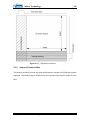
Figure 1-1
4
Interfaces and Buttons
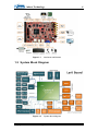
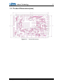
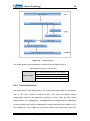
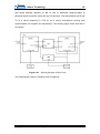
1.2 System Block Diagram
Figure 1-2
Copyright © 2014 Embest Technology
System block diagram
Lark Board User Manual
Embest Technology
5
1.3 Product Dimensions(mm)
Figure 1-3
Copyright © 2014 Embest Technology
Product Dimensions
Lark Board User Manual
Embest Technology
6
Chapter 2 Introduction to
Hardware System
This chapter will introduce in detail the structure, expansion and peripheral interfaces of
Lark Board hardware system.
2.1 Overview of CPU
Cyclone SX SoC FPGAs is the new generation developed by Altera to satisfy the demand
for products that require low power, low cost and short time-to-market, while need
high-speed and stable processing bandwidth. It not only has the logic resources of
traditional FPGAs, but also integrates a dual-core ARM Cortex A9 processor system and a
high-speed serial transceiver hard core, making it suited for the areas such as industrial
control, wireless and wired communication, medical, military and automotive electronics.
The SoC used on Lark Board is the most sophisticated FPGA chip in SX family
(5CSXFC6D6F31 in FBGA 896 package). It has three core resources:
FPGA: up to 110K logic cells (LE), 5570 M10K memory blocks, 621 MLABs, 112
variable-precision DSP blocks, 224 18x18 multipliers, 6 PLLs, 288 IOs, 72+72
LVDS transceiver, and a memory controller.
HPS: a dual-core ARM Cortex A9 MPCore processor, a memory controller
(DDR3), 3 PLLs and 181 general IOs, as well as a rich set of peripheral
interfaces such as UART, I2C, USB, SPI, GPIO and EMAC.
Serdes: 9 3Gbps transceivers and2 PCIe hard IPs.
2.2 Introduction to Peripheral Chips
2.2.1
DDR3
5CSXFC6D6F SoC has a hard memory controller separately for FPGA and HPS with a
purpose to extend more external dynamic memory spaces. Accordingly, Lark Board
Copyright © 2014 Embest Technology
Lark Board User Manual
Embest Technology
7
integrates two DDR3 SDRAM chips for FPGA and another two chips for HPS, giving each
of them 1GB external memory space.
HPS DDR3
The HMC of HPS is an effective expansion for the access space of ARM Cortex
A9 processor; It receives events come from AMBA AXI bus and Avalon-MM bus,
and converts them into proper SDRAM instructions to manage the accesses to
SDRAM.
As for hardware circuitry design, there a 73 signal lines in total on DDR3 SDRAM
interface, which includes 44 data lines (32 DQ, 4 DM, 4 pairs of DQS), 15
address lines, 11 instruction lines, 2 clock lines and 1 ZQ calibration resistive line.
Because DDR is source-synchronous time sequence interface model, the
signals related to each other require same-length traces on PCB layout to ensure
timing closure. In addition, parameters such as time sequence, driving capability
and on-chip match can be configured in Qsys, and therefore being consistent
with the physical design is required; it would be wise to add a matching resistor in
parallel on the board because the address and instruction signals are working
under two-driven-by-one mode.
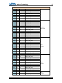
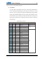
The following table contains the interface definition and signal connections of
HPS DDR3.
Table 2-1 HPS DDR3
HPS DDR3
Pin
Bank
Direction
Signal Name
M23
6A
Out
DDR3_HPS_CLK_P
L23
6A
Out
DDR3_HPS_CLK_N
F26
6A
Out
DDR3_HPS_A0
G30
6A
Out
DDR3_HPS_A1
F28
6A
Out
DDR3_HPS_A2
F30
6A
Out
DDR3_HPS_A3
J25
6A
Out
DDR3_HPS_A4
J27
6A
Out
DDR3_HPS_A5
F29
6A
Out
DDR3_HPS_A6
E28
6A
Out
DDR3_HPS_A7
Copyright © 2014 Embest Technology
Signal Type
Clock
Address
Lark Board User Manual
Embest Technology
8
HPS DDR3
H27
6A
Out
DDR3_HPS_A8
G26
6A
Out
DDR3_HPS_A9
D29
6A
Out
DDR3_HPS_A10
C30
6A
Out
DDR3_HPS_A11
B30
6A
Out
DDR3_HPS_A12
C29
6A
Out
DDR3_HPS_A13
H25
6A
Out
DDR3_HPS_A14
P30
6A
Out
DDR3_HPS_RESETn
L29
6A
Out
DDR3_HPS_CKE
H28
6A
Out
DDR3_HPS_ODT
E29
6A
Out
DDR3_HPS_BA0
J24
6A
Out
DDR3_HPS_BA1
J23
6A
Out
DDR3_HPS_BA2
E27
6A
Out
DDR3_HPS_CASn
D30
6A
Out
DDR3_HPS_RASn
H24
6A
Out
DDR3_HPS_CSn
C28
6A
Out
DDR3_HPS_WEn
D27
6A
In
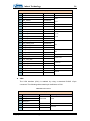
HPS_RZQ
K23
6A
IO
DDR3_HPS_DQ0
K22
6A
IO
DDR3_HPS_DQ1
H30
6A
IO
DDR3_HPS_DQ2
G28
6A
IO
DDR3_HPS_DQ3
L25
6A
IO
DDR3_HPS_DQ4
L24
6A
IO
DDR3_HPS_DQ5
J30
6A
IO
DDR3_HPS_DQ6
J29
6A
IO
DDR3_HPS_DQ7
K28
6A
IO
DDR3_HPS_DM0
N18
6A
IO
DDR3_HPS_DQS_P0
M19
6A
IO
DDR3_HPS_DQS_N0
K26
6A
IO
DDR3_HPS_DQ8
L26
6A
IO
DDR3_HPS_DQ9
K29
6A
IO
DDR3_HPS_DQ10
K27
6A
IO
DDR3_HPS_DQ11
M26
6A
IO
DDR3_HPS_DQ12
M27
6A
IO
DDR3_HPS_DQ13
L28
6A
IO
DDR3_HPS_DQ14
M30
6A
IO
DDR3_HPS_DQ15
M28
6A
IO
DDR3_HPS_DM1
N25
6A
IO
DDR3_HPS_DQS_P1
N24
6A
IO
DDR3_HPS_DQS_N1
U26
7A
IO
DDR3_HPS_DQ16
Data
T26
7A
IO
DDR3_HPS_DQ17
Group 2
Copyright © 2014 Embest Technology
Control &
Command
Data
Group 0
Data
Group 1
Lark Board User Manual
Embest Technology
9
HPS DDR3
N29
7A
IO
DDR3_HPS_DQ18
N28
7A
IO
DDR3_HPS_DQ19
P26
7A
IO
DDR3_HPS_DQ20
P27
7A
IO
DDR3_HPS_DQ21
N27
7A
IO
DDR3_HPS_DQ22
R29
7A
IO
DDR3_HPS_DQ23
R28
7A
IO
DDR3_HPS_DM2
R19
7A
IO
DDR3_HPS_DQS_P2
R18
7A
IO
DDR3_HPS_DQS_N2
P24
7A
IO
DDR3_HPS_DQ24
P25
7A
IO
DDR3_HPS_DQ25
T29
7A
IO
DDR3_HPS_DQ26
T28
7A
IO
DDR3_HPS_DQ27
R27
7A
IO
DDR3_HPS_DQ28
R26
7A
IO
DDR3_HPS_DQ29
V30
7A
IO
DDR3_HPS_DQ30
W29
7A
IO
DDR3_HPS_DQ31
W30
7A
IO
DDR3_HPS_DM3
R22
7A
IO
DDR3_HPS_DQS_P3
R21
7A
IO
DDR3_HPS_DQS_N3
Data
Group 3
FPGA DDR3
FPGA has the similar HMC which also enjoys an extended 1GB dynamic RAM;
the hardware design of FPGA DDR3 is almost the same as HPS DDR3.
The following table contains interface definition and signal connection of FPGA
DDR3.
Table 2-2 FPGA DDR3
FPGA DDR3
Pin
Bank
Direction
Signal Name
AA14
3B
Out
DDR3_FPGA_CLK_P
AA15
3B
Out
DDR3_FPGA_CLK_N
AJ14
3B
Out
DDR3_FPGA_A0
AK14
3B
Out
DDR3_FPGA_A1
AH12
3B
Out
DDR3_FPGA_A2
AJ12
3B
Out
DDR3_FPGA_A3
AG15
3B
Out
DDR3_FPGA_A4
AH15
3B
Out
DDR3_FPGA_A5
AK12
3B
Out
DDR3_FPGA_A6
Copyright © 2014 Embest Technology
Signal Type
Clock
Address
Lark Board User Manual
Embest Technology
10
FPGA DDR3
AK13
3B
Out
DDR3_FPGA_A7
AH13
3B
Out
DDR3_FPGA_A8
AH14
3B
Out
DDR3_FPGA_A9
AJ9
3B
Out
DDR3_FPGA_A10
AK9
3B
Out
DDR3_FPGA_A11
AK7
3B
Out
DDR3_FPGA_A12
AK8
3B
Out
DDR3_FPGA_A13
AG12
3B
Out
DDR3_FPGA_A14
AK21
4A
Out
DDR3_FPGA_RESETn
AJ21
4A
Out
DDR3_FPGA_CKE
AE16
4A
Out
DDR3_FPGA_ODT
AH10
3B
Out
DDR3_FPGA_BA0
AJ11
3B
Out
DDR3_FPGA_BA1
AK11
3B
Out
DDR3_FPGA_BA2
AH7
3B
Out
DDR3_FPGA_CASn
AH8
3B
Out
DDR3_FPGA_RASn
AB15
3B
Out
DDR3_FPGA_CSn
AJ6
3B
Out
DDR3_FPGA_WEn
AG17
4A
In
FPGA_RZQ
AF18
4A
IO
DDR3_FPGA_DQ0
AE17
4A
IO
DDR3_FPGA_DQ1
AG16
4A
IO
DDR3_FPGA_DQ2
AF16
4A
IO
DDR3_FPGA_DQ3
AH20
4A
IO
DDR3_FPGA_DQ4
AG21
4A
IO
DDR3_FPGA_DQ5
AJ16
4A
IO
DDR3_FPGA_DQ6
AH18
4A
IO
DDR3_FPGA_DQ7
AH17
4A
IO
DDR3_FPGA_DM0
V16
4A
IO
DDR3_FPGA_DQS_P0
W16
4A
IO
DDR3_FPGA_DQS_N0
AK18
4A
IO
DDR3_FPGA_DQ8
AJ17
4A
IO
DDR3_FPGA_DQ9
AG18
4A
IO
DDR3_FPGA_DQ10
AK19
4A
IO
DDR3_FPGA_DQ11
AG20
4A
IO
DDR3_FPGA_DQ12
AF19
4A
IO
DDR3_FPGA_DQ13
AJ20
4A
IO
DDR3_FPGA_DQ14
AH24
4A
IO
DDR3_FPGA_DQ15
AG23
4A
IO
DDR3_FPGA_DM1
V17
4A
IO
DDR3_FPGA_DQS_P1
W17
4A
IO
DDR3_FPGA_DQS_N1
AE19
4A
IO
DDR3_FPGA_DQ16
Copyright © 2014 Embest Technology
Control &
Command
Data
Group 0
Data
Group 1
Data
Lark Board User Manual
Embest Technology
11
FPGA DDR3
AE18
4A
IO
DDR3_FPGA_DQ17
AG22
4A
IO
DDR3_FPGA_DQ18
AK22
4A
IO
DDR3_FPGA_DQ19
AF21
4A
IO
DDR3_FPGA_DQ20
AF20
4A
IO
DDR3_FPGA_DQ21
AH23
4A
IO
DDR3_FPGA_DQ22
AK24
4A
IO
DDR3_FPGA_DQ23
AK23
4A
IO
DDR3_FPGA_DM2
Y17
4A
IO
DDR3_FPGA_DQS_P2
AA18
4A
IO
DDR3_FPGA_DQS_N2
AF24
4A
IO
DDR3_FPGA_DQ24
AF23
4A
IO
DDR3_FPGA_DQ25
AJ24
4A
IO
DDR3_FPGA_DQ26
AK26
4A
IO
DDR3_FPGA_DQ27
AE23
4A
IO
DDR3_FPGA_DQ28
AE22
4A
IO
DDR3_FPGA_DQ29
AG25
4A
IO
DDR3_FPGA_DQ30
AK27
4A
IO
DDR3_FPGA_DQ31
AJ27
4A
IO
DDR3_FPGA_DM3
AC20
4A
IO
DDR3_FPGA_DQS_P3
AD19
4A
IO
DDR3_FPGA_DQS_N3
2.2.2
Group 2
Data
Group 3
eMMC Flash
KE4CN2H5A is the eMMC Flash used on Lark Board with a memory space of 4GB.
2.2.3
CH7033B
CH7033B is a video encoder designed to drive high-resolution displays through HDMI,
DVI, YPbPr and VGA interfaces. It is suited for mobile Internet devices, laptops, tablet
computers, portable e-books and smart phones.
This chip possesses advanced scaling engine that supports 1080P HDTV. The integrated
frequency shifting engine can provide 60fps under 1080p mode. Additionally, CH7033B
supports SPDIF and IIS digital audio output.
2.2.4
AR8035
Copyright © 2014 Embest Technology
Lark Board User Manual
Embest Technology
12
AR8035 is a low-power and low-cost Ethernet PHY used on Lark Board and integrated
with a 10/100/1000Mb transceiver. It is a single-port tri-speed Ethernet PHY and supports
MAC.TM RGMII interfaces.
AR8035 is compliant with the IEEE 802.3az Energy Efficiency Ethernet Standard and the
Atheros’s proprietary SmartEEE standard, which allows traditional MAC/SoC devices
incompatible with 802.3az to function as a complete 802.3az system.
Lark Board can be connected to a hub with a straight-though network cable, or connected
to a computer with a crossover cable.
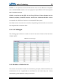
2.3 I/O Voltages
The following figure shows the number of valid I/O on each I/O bank of SoC and their
voltages applied.
Table 2-3 I/O and voltages
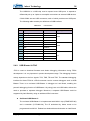
2.4 Details of Interfaces
This section will introduce in detail the constructions, principles, interface definitions and
considerations of use of peripherals on Lark Board so that users may have a deep
understanding of the hardware circuitry of the board.
Copyright © 2014 Embest Technology
Lark Board User Manual
Embest Technology
13
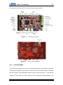
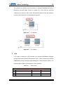
The peripheral interfaces and key on-board chips are shown below;
Figure 2-1
Figure 2-2
2.4.1
Top view of Lark Board
Bottom view of Lark Board
LCD/VGA/HDMI
The powerful video performance is one of the important features of Lark Board. It supports
multiple types of displays including 50-pin medium-/small-sized LCD modules, VGA/HDMI
and SDI monitors. LCD/VGA/HDMI shares the same video data source – Frame Buffer
created in FPGA. Now let’s take a deep look at the hardware implementation of the
Copyright © 2014 Embest Technology
Lark Board User Manual
Embest Technology
14
display function of LCD/VGA/HDMI interfaces.
Frame Buffer
The video output of Lark Board comes from a frame buffer implemented by
FPGA. The buffer has 28 signal lines in which there are 24 data lines, 3 control
lines and 1 clock line. A 50-pin LCD can be connected directly to them to display
images, while VGA/HDMI displays need the on-board chip CH7033B to convert
the data before they can display any images; SDI also receive data from the
frame buffer, but before that, conversions by the logic resources of FPGA are
required as well.
Table 2-4 Display output pins
Display Data Output
Pin
Bank
Direction
Signal Name
Signal Type
K12
8A
Out
DSS_CLK
Clock
J12
8A
Out
DSS_VSYNC
H13
8A
Out
DSS_HSYNC
G13
8A
Out
DSS_ACBIAS
E11
8A
Out
DSS_D0
D9
8A
Out
DSS_D1
E9
8A
Out
DSS_D2
B6
8A
Out
DSS_D3
B5
8A
Out
DSS_D4
D5
8A
Out
DSS_D5
C4
8A
Out
DSS_D6
B1
8A
Out
DSS_D7
D7
8A
Out
DSS_D8
E8
8A
Out
DSS_D9
E2
8A
Out
DSS_D10
D2
8A
Out
DSS_D11
C2
8A
Out
DSS_D12
E3
8A
Out
DSS_D13
E6
8A
Out
DSS_D14
F6
8A
Out
DSS_D15
G12
8A
Out
DSS_D16
G11
8A
Out
DSS_D17
G7
8A
Out
DSS_D18
H8
8A
Out
DSS_D19
G8
8A
Out
DSS_D20
Copyright © 2014 Embest Technology
Control
Data
Lark Board User Manual
Embest Technology
15
Display Data Output
J7
8A
Out
DSS_D21
H7
8A
Out
DSS_D22
H14
8A
Out
DSS_D23
LCD
The LCD interface (J4) of Lark Board is implemented with a 50-pin FPC
connector which connects LCD module to the board. Currently LCD8000-43T
(4.3 inch), LCD8000-70T (7 inch) and VGA8000 conversion module are
supported by the board. The following table contains pin definitions of LCD
interface (including the fixed pins of the connector).
Table 2-5 LCD interface
LCD Display: J4
Pin
Signal Name
Device
1
DSS_D0
5CSXFC6D
2
DSS_D1
5CSXFC6D
3
DSS_D2
5CSXFC6D
4
DSS_D3
5CSXFC6D
Data
5
DSS_D4
5CSXFC6D
Blue
6
DSS_D5
5CSXFC6D
7
DSS_D6
5CSXFC6D
8
DSS_D7
5CSXFC6D
9
GND
10
DSS_D8
5CSXFC6D
11
DSS_D9
5CSXFC6D
12
DSS_D10
5CSXFC6D
13
DSS_D11
5CSXFC6D
Data
14
DSS_D12
5CSXFC6D
Green
15
DSS_D13
5CSXFC6D
16
DSS_D14
5CSXFC6D
17
DSS_D15
5CSXFC6D
18
GND
19
DSS_D16
5CSXFC6D
20
DSS_D17
5CSXFC6D
21
DSS_D18
5CSXFC6D
22
DSS_D19
5CSXFC6D
23
DSS_D20
5CSXFC6D
24
DSS_D21
5CSXFC6D
25
DSS_D22
5CSXFC6D
Copyright © 2014 Embest Technology
Signal Type
Ground
Ground
Data
Red
Lark Board User Manual
Embest Technology
16
LCD Display: J4
26
DSS_D23
27
GND
28
DSS_ACBIAS
5CSXFC6D
29
DSS_HSYNC
5CSXFC6D
30
DSS_VSYNC
5CSXFC6D
31
GND
32
DSS_CLK
33
GND
34
TOUCH_X1
TSC2046
35
TOUCH_X1
TSC2046
Touch
36
TOUCH_X1
TSC2046
Panel
37
TOUCH_X1
TSC2046
38
SPI0_FPGA_CLK
5CSXFC6D
39
SPI0_FPGA_MOSI
5CSXFC6D
40
SPI0_FPGA_MISO
5CSXFC6D
41
SPI0_FPGA_CSn1
5CSXFC6D
42
LCD_I2C1_SCL
5CSXFC6D
43
LCD_I2C1_SDA
5CSXFC6D
44
GND
45
3.3V_LCD_VDD
46
3.3V_LCD_VDD
47
5V_LCD_VDD
48
5V_LCD_VDD
49
RESET_HPS_GLOBELn
S1
Reset
50
LCD_PWM
5CSXFC6D
Control
51
GND
52
GND
5CSXFC6D
Ground
Data
Sync
Ground
5CSXFC6D
Clock
Ground
SPI
I2C
Ground
Power 3.3V
Power 5V
Ground
VGA
The VGA interface (CN1) is realized by using a standard D-SUB 15-pin
connector. The following table contains pin definitions of CN1.
Table 2-6 VGA interface
VGA Display: CN1
Pin
Signal Name
1
VGA_REG
2
VGA_GRN
3
VGA_BLU
4
NC
5
GND
6
GND
Device
Signal Type
CH7033B
Data
Copyright © 2014 Embest Technology
Other
Ground
Lark Board User Manual
Embest Technology
17
VGA Display: CN1
7
GND
8
GND
9
VGA_VDD
Power 5V
10
GND
Ground
11
NC
Other
12
I2C_SDA_VGA
13
I2C_SCL_VGA
14
5V_HSYNC
15
5V_VSYNC
I2C
SYNC
HDMI
The HDMI interface on Lark Board is named as J5, which is a standard 19-pin
HDMI connector. The following table contains pin definitions of the interface
(including the fixed pins of the connector).
Table 2-7 HDMI interface
Pin
1
2
3
4
5
6
7
8
9
10
11
12
13
14
15
16
17
18
19
20
21
22
Signal Name
HDMI_TX2+
GND
HDMI_TX2HDMI_TX1+
GND
HDMI_TX1HDMI_TX0+
GND
HDMI_TX0HDMI_CLK+
GND
HDMI_CLKNC
NC
HDMICONN_I2CSCL
HDMICONN_I2CSDA
GND
5V_VDD
HDMICONN_HPLG
GND_SHELDS
GND_SHELDS
GND_SHELDS
HDMI Display: J5
Device
CH7033B
CH7033B
CH7033B
CH7033B
CH7033B
CH7033B
CH7033B
CH7033B
CH7033B
CH7033B
CH7033B
CH7033B
Copyright © 2014 Embest Technology
Signal Type
Differential
Data & Clock, GND as
reference for signal
Other
TXS0102DC
TXS0102DC
5CSXFC6D
I2C
Ground
Power 5V
Status
Ground
Lark Board User Manual
Embest Technology
18
HDMI Display: J5
23
2.4.2
GND_SHELDS
SDI
The SDI interface on Lark Board is used to implement high-resolution video input and
output, which means that it could be connected to a HD camera or display. There are two
SMB connectors on the board for connections to SDI devices through co-axial cables. J10
is an output interface which is the destination of the signal that travels from SoC’s serial
transmitter to LMH0303 driver. J11 is an input interface that receives high-resolution serial
signal from external devices and passes it to LMH0384 equalizer which provides input to
SoC’s serial receiver.
The connections between SoC and LMH0303/LH0384 are shown in the following table;
Table 2-8 SDI input/output
SDI Input & Output:
2.4.3
Pin
Bank
Direction
Signal Name
T4
GXB_L1
Out
SDI_TX_P
L4
GXB_L1
Out
SDI_TX_N
C13
8A
Out
SDI_TX_SH_HDn
E13
8A
Out
SDI_RSTIn
F13
8A
In
SDI_FAULTn
F14
8A
Out
SDI_TX_EN
F15
8A
IO
SDI_I2C_SDA
B12
8A
Out
SDI_I2C_SCL
U2
GXB_L1
In
SDI_RX_P
U1
GXB_L1
In
SDI_RX_N
E12
8A
Out
SDI_RX_BYPASS
D12
8A
Out
SDI_RX_EN
Signal Type
SDI Out
SDI In
PCIe
5CSXFC6D6F SoC integrates 2 PCIe hard IPs and 9 pairs of 3Gbps serial transceiver.
Lark Board has a PCIe X1/X4 (J1) connector on board to make part of the SoC’s IPs
available for various PCIe X1/X4-compliant expansion boards.
Copyright © 2014 Embest Technology
Lark Board User Manual
Embest Technology
19
The following table contains pin definitions of the PCIe connector;
Table 2-9 PCIe connector
PCIe Connector: J1
Pin
Signal Name
A1
12V_EXP
A2
12V_EXP
A3
12V_EXP
A4
GND
A5
NC
A6
NC
A7
NC
A8
NC
A9
3.3V_EXP
A10
3.3V_EXP
A11
PCIE_RSTn
A12
GND
A13
Signal Type
Power 12V
Other
Power 3.3V
5CSX6D6F
Reset
PCIE_REFCLK_SYN_P
100M_OSC
Differential clock and
A14
PCIE_REFCLK_SYN_N
100M_OSC
reference ground
A15
GND
A16
PCIE_RX_P0
5CSX6D6F
A17
PCIE_RX_N0
5CSX6D6F
A18
GND
A19
NC
A20
GND
A21
PCIE_RX_P1
5CSX6D6F
A22
PCIE_RX_N1
5CSX6D6F
A23
GND
RX differential data and
A24
GND
reference ground
A25
PCIE_RX_P2
5CSX6D6F
A26
PCIE_RX_N2
5CSX6D6F
A27
GND
A28
GND
A29
PCIE_RX_P3
5CSX6D6F
A30
PCIE_RX_N3
5CSX6D6F
A31
GND
A32
NC
B1
12V_EXP
B2
12V_EXP
B3
12V_EXP
B4
GND
B5
PCIE_SMBCLK
Copyright © 2014 Embest Technology
Power 12V
5CSX6D6F
Control
Lark Board User Manual
Embest Technology
20
PCIe Connector: J1
2.4.4
B6
PCIE_SMBDAT
5CSX6D6F
B7
GND
Ground
B8
3.3V_EXP
Power 3.3V
B9
3.3V_EXP (Pull-up)
Status
B10
3.3V_EXP
Power 3.3V
B11
PCIE_WAKEn
B12
NC
B13
GND
B14
PCIE_TX_P0
5CSX6D6F
TX Differential data and
B15
PCIE_TX_P1
5CSX6D6F
reference ground
B16
GND
B17
PCIE_PRSNT2_X1
5CSX6D6F
Status
B18
GND
B19
PCIE_TX_P0
5CSX6D6F
B20
PCIE_TX_P1
5CSX6D6F
B21
GND
B22
GND
B23
PCIE_TX_P0
5CSX6D6F
TX Differential data and
B24
PCIE_TX_P1
5CSX6D6F
reference ground
B25
GND
B26
GND
B27
PCIE_TX_P0
5CSX6D6F
B28
PCIE_TX_P1
5CSX6D6F
B29
GND
B30
NC
B31
PCIE_PRSNT2_X4
B32
GND
5CSX6D6F
Control
Other
Other
5CSX6D6F
Status
Ground
Camera
The 30-pin FPC connector (J12) on Lark Board is used to support 12-bit input of digital
cameras. It is currently compatible with Embest’s CAM8000-D camera module.
The following table contains pin definitions of the FPC connector;
Table 2-10
FPC connector
Camera(J12)
Pin
Signal Name
1
GND
2
CAM_D0
Copyright © 2014 Embest Technology
Device
Signal Type
Ground
5CSXFC6D
Data
Lark Board User Manual
Embest Technology
21
Camera(J12)
2.4.5
3
CAM_D1
4
CAM_D2
5
CAM_D3
6
CAM_D4
7
CAM_D5
8
CAM_D6
9
CAM_D7
10
CAM_D8
11
CAM_D9
12
CAM_D10
13
CAM_D11
14
GND
15
PCLK
16
GND
17
CAM_HS
18
GND
19
CAM_VS
20
3.3V_CAMERA
21
CAM_CLK
22
CAM_CLK1
23
GND
24
CAM_FLD
5CSXFC6D
25
CAM_WEN
5CSXFC6D
26
CAM_STROBE
5CSXFC6D
27
CAM_SDA
28
CAM_SCL
29
GND
Ground
30
3.3V_CAMERA_IO
Power 3.3V
31
GND
32
GND
Ground
5CSXFC6D
Clock
Ground
5CSXFC6D
SYNC
Ground
5CSXFC6D
SYNC
Power 3.3V
5CSXFC6D
Clock
Ground
TXS0102D
Status
I2C
Power
ADC & Pre-Amp
Since a long time ago, FPGA is always involved in data acquisition, especially in the
high-speed applications, the data acquisition systems built up with FPGA and ADC can be
often found. Lark Board has a data acquisition system prototype which is made up of
high-bandwidth amplifier, anti-alias filter, high-speed ADC, FPGA and ARM to support
dual-channel single-ended analog signal based on SMA input or differential analog signal.
Copyright © 2014 Embest Technology
Lark Board User Manual
Embest Technology
22
Pre-Amp
The pre-amp circuitry is used to receive and amplify analog input. Lark Board
provides two analog input channels that support single-ended SMA input or
differential input.
Figure 2-3
Pre-Amp circuitry
As shown in the figure above, pre-amp circuitry is made up of a Balun (T46) and
a balanced filtering circuit. The jumpers JP1 and JP3 are used to select working
mode of Balun. When JP1 and JP3 are both opened, J6 and J7 constitute a
differential channel A, J8 and J9 constitute channel B; When JP1 and JP3 are
both shorted, J6 input is a single-ended channel A and J8 is a single-ended
channel B. The resistors R159, R158, R166, and R168 are used to set the gains
of amplifier ADL5562 to 6dB, 12dB or 15.5dB. (For more details, please refer to
ADL5562 datasheet)
Figure 2-4
Amplification output circuit
Copyright © 2014 Embest Technology
Lark Board User Manual
Embest Technology
23
As shown in the figure above, an optimized third-order butterworth anti-alias filter
is placed between amplifier output end and ADC.
ADC
The ADC AD962 can provide a capability of 12-bit, 105MSPS sampling
performance and support quantified data output of CMOS or LVDS.
The following table contains pin definitions and signal connections between ADC
and FPGA;
Table 2-11
Interface between ADC and FPGA
Interface between ADC & FPGA
Pin
Bank
Direction
Signal Name
AE29
5B
Out
ADC_CLK105_P
AD29
5B
Out
ADC_CLK105_N
W25
5B
In
ADC_Dp0
V25
5B
In
ADC_Dn0
Y26
5B
In
ADC_Dp1
Y27
5B
In
ADC_Dn1
V23
5A
In
ADC_Dp2
W24
5A
In
ADC_Dn2
AA26
5B
In
ADC_Dp3
AB27
5B
In
ADC_Dn3
AA24
5A
In
ADC_Dp4
AB25
5A
In
ADC_Dn4
W21
5A
In
ADC_Dp5
W22
5A
In
ADC_Dn5
Differential
AD26
5A
In
ADC_Dp6
Data
AC27
5A
In
ADC_Dn6
AA13
3B
In
ADC_Dp7
AB13
3B
In
ADC_Dn7
Y23
5A
In
ADC_Dp8
Y24
5A
In
ADC_Dn8
AD25
5A
In
ADC_Dp9
AC25
5A
In
ADC_Dn9
AF11
3B
In
ADC_Dp10
AG11
3B
In
ADC_Dn10
AB22
5A
In
ADC_Dp11
AB23
5A
In
ADC_Dn11
W20
5A
Out
ADC_ORp
Differential
Y21
5A
Out
ADC_ORn
Status
Copyright © 2014 Embest Technology
Signal Type
Clock
Lark Board User Manual
Embest Technology
24
Interface between ADC & FPGA
2.4.6
AB30
5B
In
ADC_DCOp
AA30
5B
In
ADC_DCOn
AE13
3B
In
ADC_D0B
AK4
3B
In
ADC_D1B
Single-Ended
AJ4
3B
In
ADC_D2B
Data
AK3
3B
In
ADC_D3B
AF30
5A
Out
FPGA_ADC_OEB
AD24
4A
Out
FPGA_ADC_SPICSn
AE24
4A
Out
FPGA_ADC_SPICLK
AC23
4A
Out
FPGA_ADC_SPIMOSI
SPI
Gigabit Ethernet
Lark Board can provide a relatively high network performance of gigabit Ethernet. The
Ethernet is implemented by utilizing part of the EMAC controller integrated in HPS. The
AR8035 is added to realize connections between PHY and EMAC. The RJ-45 interface is
named as J14 to provide connection to network devices.
RGMII
RGMII is the interfacing protocol applied on the connection between EMAC and
AR8035 (PHY). It uses a 4-bit data port and operates at 125MHz. It supports
data transmission at both rising edge and fall edge, providing a transmission rate
up to 1000Mbps. The following table contains pin definitions of RGMII interface
on Lark Board.
Table 2-12
Interface between HPS MAC and PHY
Interface between HPS MAC & PHY
Pin
Bank
Direction
Signal Name
H19
7B
Out
MII1_TX_CLK
A20
7B
Out
MII1_TX_EN
F20
7B
Out
MII1_TXD0
J19
7B
Out
MII1_TXD1
F21
7B
Out
MII1_TXD2
F19
7B
Out
MII1_TXD3
G20
7B
In
MII1_RX_CLK
K17
7B
In
MII1_RX_DV
A21
7B
In
MII1_RXD0
Copyright © 2014 Embest Technology
Signal Type
TX
Rx
Lark Board User Manual
Embest Technology
25
Interface between HPS MAC & PHY
B20
7B
In
MII1_RXD1
B18
7B
In
MII1_RXD2
D21
7B
In
MII1_RXD3
B21
7B
Out
MII_MDC
E21
7B
IO
MII_MDIO
C19
7B
In
MII_INT
Manage
RJ-45
The following table contains pin definitions of RJ-45 (J14) Ethernet interface;
Table 2-13
Ethernet interface
RJ45 Ethernet: J14
2.4.7
Pin
Signal Name
1
MIIA_TRP0
2
MIIA_TRN0
3
MIIA_TRP1
4
MiIA_TRN1
5
NC
6
NC
7
MIIA_TRP2
8
MIIA_TRN2
9
MIIA_TRP3
10
MIIA_TRN3
11
MIIA_LED_LINK
12
Pull-down
13
MIIA_LED_ACT
14
Pull-up
15
GND
16
GND
17
NC
18
NC
Device
Signal Type
AR8035
Data
Shield
AR8035
Data
LED Control
LED
GND
Fix
eMMC& TF Card
eMMC and TF card are used to provide solid storage of boot code and system.
Although there is only one MMC/SD controller in HPS, TF card and eMMC could
work alternatively by the help of eMMC/TF card power switch design on Lark
Board.
Copyright © 2014 Embest Technology
Lark Board User Manual
Embest Technology
26
eMMC Interface
eMMC and TF card share the MMC/SD controller of HPS, so they work on the
same clock, lower 4-bit data and control signal, but the higher 4-bit data is
reserved for eMMC. The following table contains pin definitions of eMMC
interface
Table 2-14
eMMC interface
eMMC between HPS & Device
Pin
Bank
Device
Signal Name
G18
7C
IO
MMC_DAT0
C17
7C
IO
MMC_DAT1
D17
7C
IO
MMC_DAT2
B16
7C
IO
MMC_DAT3
H17
7C
IO
MMC_DAT4
C18
7C
IO
MMC_DAT5
G17
7C
IO
MMC_DAT6
E18
7C
IO
MMC_DAT7
A16
7C
Out
MMC_CLK
F18
7C
Out
MMC_CMD
B17
7C
Out
MMC_CD
Signal Type
Data
Clock
Control
TF Card Interface
The TF1 interface on the back of Lark Board is a TF card slot. The following table
contains pin definitions of the interface;
Table 2-15
TF card interface
TF card connector: TF1
Pin
Signal Name
Device
1
MMC_DAT2
5CSX6F6D
2
MMC_DAT3
5CSX6F6D
3
MMC_CMD
5CSX6F6D
4
3.3V_VDD
5
MMC_CLK
6
GND
7
MMC_DAT0
5CSX6F6D
8
MMC_DAT1
5CSX6F6D
9
MMC_CD
5CSX6F6D
10
GND
11
GND
Copyright © 2014 Embest Technology
Signal Type
Data
Command
Power 3.3V
5CSX6F6D
Clock
Ground
Data
Command
Ground
Lark Board User Manual
Embest Technology
27
TF card connector: TF1
2.4.8
12
GND
13
GND
14
NC
15
NC
Fixed
USB PHY & HUB
To satisfy diverse applications involving USB interfaces, Lark Board provides 4 USB ports.
However, there are only 2 USB controllers in HPS, thus a PHY and a HUB are added to
ensure 4 USB port can work at the same time. The USB3320 on Lark Board is used to
implement ULPI protocol between PHY and controller. The USB2514 is used to expand
the ports of PHY. The following contents will introduce the implementation of USB in
detail.
USB PHY
USB3320 is an on-board USB PHY chip which exchange data with the controller
of HPS by using ULPI protocol. The following table contains pin definitions of
ULPI interface;
Table 2-16
ULPI interface
ULPI between USB Controller and PHY
Pin
Bank
Direction
Signal Name
E16
7D
IO
USB1HS_D0
G16
7D
IO
USB1HS_D1
D16
7D
IO
USB1HS_D2
D14
7D
IO
USB1HS_D3
A15
7D
IO
USB1HS_D4
C14
7D
IO
USB1HS_D5
D15
7D
IO
USB1HS_D6
M17
7D
IO
USB1HS_D7
N16
7D
IO
USB1HS_CLK
A14
7D
In
USB1HS_NXT
E14
7D
In
USB1HS_DIR
C15
7D
Out
USB1HS_STP
Signal Type
Data
Clock
Control
USB HUB
Copyright © 2014 Embest Technology
Lark Board User Manual
Embest Technology
28
The USB2514 is a HUB chip used to expand more USB ports. It expands a
differential pair up to 4 pairs to accomplish connections to external USB devices.
CON1/CON2 are two USB connectors, each of which provides two USB ports.
The following table contains pin definitions of USB interface.
Table 2-17
USB interface
USB Connector: CON1/CON2
2.4.9
Pin
Signal Name
Device
1
VBUS1_CN
2
DN1
USB2514
3
DP1
USB2514
4
GND
5
VBUS2_CN
6
DN2
USB2514
7
DP2
USB2514
8
GND
9
GND_SHIELDS
10
GND_SHIELDS
11
GND_SHIELDS
12
GND_SHIELDS
Signal Type
USB1
USB2
FIX
USB Blaster & JTAG
JTAG is used to download firmware and obtain debugging information during FPGA
development. It is very important in product development stage. The debugging function
mainly depends on the four signals: TCK, TMS, TDI and TDO. The standard debugging
interface for Altera FPGA is a 5Px2 connector used to connect debuggers such as USB
Blaster. There is an on-board USB Blaster II debugger on Lark Board, enabling the
powerful debugging function of USB Blaster II by using just a mini-USB cable, without the
need to purchase a separate debugger. Moreover, a separate USB Blaster could be
supported by Lark Board by using an additional 5Px2 connector.
On-Board USB Blaster II
The on-board USB Blaster II is implemented with MAX II chip (EPM570GF100)
and a controller (CY7C68013A). The IP authorized by Altera needs to be
programmed into MAX II. Embest has obtained that authorization on Lark Board.
Copyright © 2014 Embest Technology
Lark Board User Manual
Embest Technology
29
The CON3 on the board is used to connect to a computer installed with Quartus
through a mini-USB cable. There is a jumper JP7 near CON3 for selecting
components involved in JTAG chain. The following figures show the detection
results of SoC chip when JP7 is shorted and opened.
Figure 2-5
JP7 shorted
Figure 2-6
JP7 opened
JTAG
J3 is used to connect the JTAG interface of an external USB Blaster debugger
(please note that the position and direction of pin 1 when connector an external
USB Blaster; wrong connection might damage the JTAG interface of SoC). The
following table contains pin definitions of JTAG interface.
Table 2-18
JTAG interface
JTAG Connector: J3
Pin
Signal Name
Device
Signal Type
1
JTAG_TCK
5CSX6D6F
JTAG
2
USB_DISABLEn
3
JTAG_TDI
Copyright © 2014 Embest Technology
Control
5CSX6D6F
JTAG
Lark Board User Manual
Embest Technology
30
JTAG Connector: J3
4
3.3V_VDD
Power
5
JTAG_TMS
5CSX6D6F
JTAG
6
HPS_WARM_RSTn
JP5
Control
7
NC
8
NC
9
FPGA_TDI
5CSX6D6F
JTAG
10
GND
Ground
2.4.10 DIP Switch
There are 5 DIP switches on Lark Board for power supply control, HPS boot selection,
FPGA configuration mode selection and SDI rate selection. The following contents will
introduce the function, connections and signal definitions of each DIP switch(the DIP
Switches location as show below).
Figure 2-7
DIP Switches Location
S8 is connected to the general I/O of FPGA Bank 8A and cam be used as a typical status
input switch.
Table 2-1 DIP switch 1
Switch Pin
Signal Name
Copyright © 2014 Embest Technology
Function
Lark Board User Manual
Embest Technology
31
S8: User FPGA Dip Switch
1
USER_FPGA_DIPSW0
C8, function defined by user
2
USER_FPGA_DIPSW1
B8, function defined by user
3
USER_FPGA_DIPSW2
C10, function defined by user
4
USER_FPGA_DIPSW3
C9, function defined by user
S9 and S10 are used to enable and disable various voltages on the board. When a
voltage is disabled or unavailable, a LED in the corresponding power supply area will be
turned on, indicating the voltage has been disabled or unavailable.
Table 2-2 DIP switch 2
Switch Pin
Signal Name
Function
S9: Power on/off for 5V/12V/3.3V/2.5V
1
5V_SHDNn
On: disable 5V; Off: enable 5V
2
12V_SHDNn
On: disable 12V; Off: enable 12V
3
3.3V_POWER_EN
On: disable 3.3V; Off: enable 3.3V
4
2.5V_POWER_EN
On: disable 2.5V; Off: enable 2.5V
S10: Power on/off for 1.8V/1.1V/1.5V/VTT
1
1.8V_POWER_EN
On: disable 1.8V; Off: enable 1.8V
2
1.1V_POWER_EN
On: disable 1.1V; Off: enable 1.1V
3
1.5V_POWER_EN
On: disable 1.5V; Off: enable 1.5V
4
VTT_POWER_EN
On: disable 0.75V; Off: enable 0.75V
S11 is used to select clock and booting of HPS; the default configurations on Lark Board
are CLKSEL1/0=00 and BOOTSEL2/1/0=101.
Table 2-3 DIP switch 3
Switch Pin
Signal Name
Function
S11: Boot Device Select & Clock Select
HPS_UART0_RX
Default: CLKSEL0=0
1
HPS_GPIO62
Off:CLKSEL1=1; On:CLKSEL1=0
2
HPS_SPIM0_CS0n
Off:BOOTSEL0=1; On:BOOTSEL0=0
3
QSPI_SS0
Off:BOOTSEL1=1; On:BOOTSEL1=0
4
HPS_GPIO28
Off:BOOTSEL2=1; On:BOOTSEL2=0
The figure shown below is the configurations of CSEL and BSEL provided in Cyclone V
datasheet.
Copyright © 2014 Embest Technology
Lark Board User Manual
Embest Technology
Figure 2-8
Figure 2-9
32
CSEL pin
BSEL
S12 is used to select FPGA configuration mode. The default FPGA configuration mode on
Lark Board is MSEL[4:0]=00000.
Table 2-4 DIP switch 4
Switch Pin
Signal Name
Function
S12: FPGA Configuration Scheme
1
MSEL0
On: MSEL0=0; Off: MSEL0=1
2
MSEL1
On: MSEL1=0; Off: MSEL0=1
3
MSEL2
On: MSEL2=0; Off: MSEL0=1
4
MSEL3
On: MSEL3=0; Off: MSEL0=1
MSEL4
Default: MSEL4=0
The figure shown below can be found in Cyclone V datasheet. It lists all the configuration
modes supported by FPGA.
Copyright © 2014 Embest Technology
Lark Board User Manual
Embest Technology
Figure 2-10
33
FPGA configurations
2.4.11 Jumpers
There are jumpers on Lark Board used for function selection and expansion. The following
table contains pin definitions of each jumper.
Table 2-5 Jumpers
Jumper Function
JP Name
Signal Name
Function
JP7
JTAG_HPS_EN
Enable/disable HPS in JTAG chain
JP5
HPS_WARM_RSTn
HPS warm reset
JP1
ADC1_MODE
Analog CH1 SE/Diff mode selection
JP3
ADC2_MODE
Analog CH2 SE/Diff mode selection
JP8
FPGA_DCLK
JP9
FPGA_AS_DATA1
JP10
FPGA_AS_DATA2
JP11
FPGA_AS_DATA3
Extend for EPCQ
2.4.12 Buttons
Copyright © 2014 Embest Technology
Lark Board User Manual
Embest Technology
34
There are 6 buttons on Lark Board. S1 button can reset the board. The rest of the buttons
are used as status input of FPGA or HPS and can be programmed by users. The following
table contains signal definitions and connections of these buttons.
Table 2-6 Buttons
Button Switch Function
Switch Name
Signal Name
Function
S1
PB_COLD_RESETn
HPS & Peripheral Cold Reset
S2
USER_FPGA_PB0
Bank 3A, AH3, function defined by FPGA
S3
USER_HPS_PB0
Bank 6B, T30, function defined by HPS
S4
USER_HPS_PB1
Bank 6B,U28, function defined by HPS
S5
USER_HPS_PB2
Bank 6B, T21, function defined by HPS
S6
USER_HPS_PB3
Bank 6B, U20, function defined by HPS
2.4.13 UART
J24 and J25 are two connectors in different types specially provided on Lark Board (the
connectors cannot be used simultaneously). They are used to connect 3.3V serial
debuggers, for example, the COM8000 (DB9 to TTL) or UART-8000U (USB to TTL)
supplied by Embest. Users can use Dupont wires to connect a RS232-to-3.3V level serial
converter to conduct debugging. The following table contains pin definitions of J24 and
J25.
Table 2-7 UART
Pin
Signal Name
Device
Signal Type
J24
1
3.3V_VDD
Power 3.3V
2
HPS_UART0_TX
5CSX6D6F
3
HPS_UART0_RX
5CSX6D6F
4
GND
Ground
1
3.3V_VDD
Power 3.3V
2
HPS_UART0_TX
5CSX6D6F
3
HPS_UART0_RX
5CSX6D6F
4
GND
Ground
5
GND
Ground
UART
J25
Copyright © 2014 Embest Technology
UART
Lark Board User Manual
Embest Technology
35
2.4.14 LED
The LEDs on Lark Board can be used for programming by users and indicating board
status. The users’ LEDs include 4 HPS LEDs, 4 FPGA LEDs and 2 PCIe LEDs. The status
LEDs are used to monitor or indicate operating state of circuitry and include 7 power
indicators, 2 UART LEDs, 2 PCIe LEDs and 1 SDI LED.
The following table contains the I/O connections of HPS/FPGA user LEDs.
Table 2-8 User LEDs
FPGA Pin
Bank
LED Ref
Signal Name
A24
7A
D27
USER_HPS_LED0
G21
7A
D28
USER_HPS_LED1
E17
7A
D29
USER_HPS_LED2
G22
7A
D30
USER_HPS_LED3
HPS User LED
FPGA User LED
A4
8A
D31
USER_FPGA_LED0
A3
8A
D32
USER_FPGA_LED1
D6
8A
D33
USER_FPGA_LED2
C5
8A
D34
USER_FPGA_LED3
The following table contains the connections of status LEDs.
Table 2-9 Status LEDs
LED Ref
Signal Name
LED Function
D64
12V_POWER_GOOD
Bright indicate 12V fail
D65
5V_POWER_GOOD
Bright indicate 5V fail
D66
1.1V_POWER_GOOD
Bright indicate 1.1V fail
D67
1.8V_POWER_GOOD
Bright indicate 1.8V fail
D68
VTT_POWER_GOOD
Bright indicate 0.75V fail
D69
1.5V_POWER_GOOD
Bright indicate 1.5V fail
D70
3.3V_POWER_GOOD
Bright indicate 3.3V fail
D71
2.5V_POWER_GOOD
Bright indicate 2.5V fail
D63
POWER_GOOD
Bright indicate power OK
D35
PCIE_LED_X1
Bright indicate PCIe X1 work
D36
PCIE_LED_X4
Bright indicate PCIe X4 work
HPS_UART_RX
Blink indicate RX data active
Power LED
PCIe LED
UART LED
D15
Copyright © 2014 Embest Technology
Lark Board User Manual
Embest Technology
36
LED Ref
Signal Name
LED Function
D16
HPS_UART_TX
Blink indicate TX data active
SDI_RX_CDn
Bright indicate SDI input active
SDI LED
D6
2.4.15 RTC
There is a RTC circuitry on Lark Board. When a battery is inserted in BT1, the board can
keep a proper clock after power supply is turned off. A CR1220 battery and a DS3221 chip
are involved in the implementation of RTC circuitry. Please refer to schematics and
datasheet for its working principle and detailed circuit.
2.4.16 Extension Interfaces
To facilitate users’ function expansion, part of I/O resources of FPGA and HPS has been
extended by using two 40-pin connectors. This section will introduce these interfaces in
detail.
HPS Extension
J21 is the I/O extension interface for HPS. It uses a 40-pin 2.54mm IDC
connector to connect to Bank 7A/7B/7C/7D which are attached to some of the
HPS’s controllers such as QSPI, UART, I2C and SPI. Certainly, most of them can
be set as GPIOs. The following table contains pin definitions of J21.
Table 2-10
HPS extension interface
HPS Extend 40Pin IDC Connector: J21
Pin
Direction
Signal Type
Signal Name
1
P
Power
5V_EXP3
2
G
Ground
GND
3
N
NC
NC
4
N
NC
NC
5
P
Power
3.3V_EXP3
6
N
NC
NC
7
G
Ground
GND
8
N
NC
NC
9
OUT
UART0
HPS_UART0_RX
Copyright © 2014 Embest Technology
Pin_FPGA
Bank FPGA
D24
7A
Lark Board User Manual
Embest Technology
37
HPS Extend 40Pin IDC Connector: J21
10
G
NC
GND
11
IO
GPIO
HPS_GPIO0
F16
12
IN
UART0
HPS_UART0_TX
E24
7A
13
IN
I2C0
HPS_I2C0_SCL
E23
7A
14
IO
GPIO
HPS_GPIO9
B15
7D
15
OUT
UART1
HPS_UART1_RX
D22
7A
16
IO
I2C0
HPS_I2C0_SDA
C24
7A
17
G
Ground
GND
18
IN
UART1
HPS_UART1_TX
C23
7A
19
IO
QSPI
QSPI_IO0
C20
7B
20
G
Ground
GND
21
IO
QSPI
QSPI_IO1
H18
7B
22
IO
GPIO
HPS_GPIO49
B25
7A
23
IO
QSPI
QSPI_IO2
A19
7B
24
IO
GPIO
HPS_GPIO50
C25
7A
25
IO
QSPI
QSPI_IO3
E19
7B
26
IO
GPIO
HPS_GPIO53
A24
7A
27
IN
QSPI
QSPI_SS0
A18
7B
28
IO
GPIO
HPS_GPIO54
G21
7A
29
IN
QSPI
QSPI_CLK
D19
7B
30
IO
GPIO
HPS_GPIO44
E17
7C
31
G
Ground
GND
32
IO
GPIO
HPS_GPIO62
G22
7A
33
IN
I2C1
HPS_I2C1_SCL
H23
7A
34
G
Ground
GND
35
IN
SPI
HPS_SPIM0_MOSI
C22
7A
36
IO
I2C1
HPS_I2C1_SDA
A25
7A
37
IN
SPI
HPS_SPIM0_CLK
A23
7A
38
OUT
SPI
HPS_SPIM0_MISO
B23
7A
39
IN
SPI
HPS_SPIM0_CS0n
H20
7A
40
IO
GPIO
HPS_GPIO61
B22
7A
FPGA Extension
J19 is the I/O extension interface for FPGA and transceiver. It uses the same
type of connector, to connect Bank 8A/GXB_L1/GXB_L2. The GXB can use the
hard IP controller of FPGA such as PCIe; the I/O of 8A works on 3.3V level and
can use various resources of FPGA IO such as PLL and M4K. The following
table contains pin definition of J19.
Table 2-11
Copyright © 2014 Embest Technology
FPGA extension interface
Lark Board User Manual
Embest Technology
38
FPGA Extend 40Pin IDC Connector: J18
Pin
Direction
Signal Type
Signal Name
Pin_FPGA
Bank FPGA
1
P
Power
5V_EXP2
2
G
Ground
GND
3
IN
Control
nPERSTL0
AJ1
3A
4
IN
Control
FPGA_H_SMBCLK
E7
8A
5
G
Ground
GND
6
IO
Control
FPGA_H_SMBDAT
H12
8A
7
IO
Data
FPGA_RX_H_P0
R2
GXB_L1
8
IO
Data
FPGA_TX_H_P0
P4
GXB_L1
9
IO
Data
FPGA_RX_H_N0
R1
GXB_L1
10
IO
Data
FPGA_TX_H_N0
P3
GXB_L1
11
IO
Data
FPGA_RX_H_P1
N2
GXB_L2
12
IO
Data
FPGA_TX_H_P1
M4
GXB_L2
13
IO
Data
FPGA_RX_H_N1
N1
GXB_L2
14
IO
Data
FPGA_TX_H_N1
M3
GXB_L2
15
IO
Data
FPGA_RX_H_P2
L2
GXB_L2
16
IO
Data
FPGA_TX_H_P2
K4
GXB_L2
17
IO
Data
FPGA_RX_H_N2
L1
GXB_L2
18
IO
Data
FPGA_TX_H_N2
K3
GXB_L2
19
IO
Data
FPGA_RX_H_P3
J2
GXB_L2
20
IO
Data
FPGA_TX_H_P3
H4
GXB_L2
21
IO
Data
FPGA_RX_H_N3
J1
GXB_L2
22
IO
Data
FPGA_TX_H_N3
H3
GXB_L2
23
G
Ground
GND
24
G
Ground
GND
25
IO
Data
FPGA_RX_D_P0
K7
8A
26
IO
Data
FPGA_TX_D_P0
C7
8A
27
IO
Data
FPGA_RX_D_N0
K8
8A
28
IO
Data
FPGA_TX_D_N0
B7
8A
29
IO
Data
FPGA_RX_D_P1
J10
8A
30
IO
Data
FPGA_TX_D_P1
A9
8A
31
IO
Data
FPGA_RX_D_N1
J9
8A
32
IO
Data
FPGA_TX_D_N1
A8
8A
33
IO
Data
FPGA_RX_D_P2
F9
8A
34
IO
Data
FPGA_TX_D_P2
C12
8A
35
IO
Data
FPGA_RX_D_N2
F8
8A
36
IO
Data
FPGA_TX_D_N2
B11
8A
37
IO
Data
FPGA_RX_D_P3
G10
8A
38
IO
Data
FPGA_TX_D_P3
B13
8A
39
IO
Data
FPGA_RX_D_N3
F10
8A
40
IO
Data
FPGA_TX_D_N3
A13
8A
Copyright © 2014 Embest Technology
Lark Board User Manual
Embest Technology
39
Chapter 3 Quick Use of Lark
Board
Lark Board eMMC Flash has been installed with Yocto image by default so that the board
could be booting and running immediately. This chapter will introduce how to realize a
quick use of Lark Board through simple hardware connections and software
configurations. Please follow the quick steps listed below.
1) Set the DIP switches as shown in the following figure;
Figure 3-1
DIP switch settings
2) Connect a USB-To-TTL conversion cable (for example UART8000-U; needs to be
purchased separately) to the serial port of Lark Board as shown below:
Copyright © 2014 Embest Technology
Lark Board User Manual
Embest Technology
Figure 3-2
40
Hardware connections
3) Connect the UART8000-U to the USB Host on PC and refer the UART8000-U user
manual to install the driver, then power on the board; After Lark Board boots up, it will
obtain a port number, for example com10, allocated automatically by PC to the
board,;
4) PuTTY will be taken as the example of serial communication software to explain how
to
configure
parameters.
Firstly,
download
PuTTY
from
http://www.chiark.greenend.org.uk/~sgtatham/putty/download.html, then install and
run it on a PC;
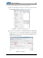
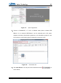
5) In the pop-up configuration window, please select Serial radio box under Connection
type; enter the serial port number (COM10 for example) allocated by the PC in Serial
line text box and 115200 in Speed text box; (you can enter a name, for example
serial-com10, for the current session in Saved Sessions text box and then click Save
to save the configurations under the name you entered)
Copyright © 2014 Embest Technology
Lark Board User Manual
Embest Technology
Figure 3-3
41
Enter port number
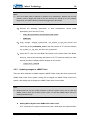
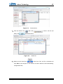
6) Click Window entry on the left part of configuration window and change the
Lines of scrollback to 50000 on the right part as shown below; This would
prevent printed texts from being overlapped with each other because of
inadequate printing lines allowed in PuTTY terminal window;
Copyright © 2014 Embest Technology
Lark Board User Manual
Embest Technology
Figure 3-4
42
Window configuration
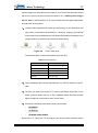
7) Click Serial entry on the left part of the window and configure serial lines as
shown below; When configuration is done, click Open to enter PuTTY terminal
window;
Copyright © 2014 Embest Technology
Lark Board User Manual
Embest Technology
Figure 3-5
43
Serial configuration
8) Now the serial connection between PuTTY and Lark Board has been established;
PuTTY terminal window will print booting information when Lark Board is
rebooting; To implement operations on Lark Board, you just need to type
instructions in the window;
Copyright © 2014 Embest Technology
Lark Board User Manual
Embest Technology
44
Chapter 4 Linux
This chapter will briefly introduce the Linux system structure of Lark Board, available
software resources, building of development environment, system image compilation and
update, drivers’ paths and working principles, function tests and application development.
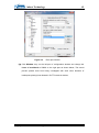
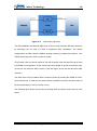
4.1 Linux System Structure of Lark Board
The embedded Linux system of Lark Board is composed of four blocks: Preloader, U-boot,
Kernel and Rootfs; the following figure is an illustration of the structure, followed with brief
description for each block.
Figure 4-1
Embedded Linux system structure
Preloader: It is a primary bootstrap; when system boots up, it is copied from
HPS boot ROM to on-chip RAM to be executed. It is responsible for initializing
CPU, copying u-boot to SDRAM, and then hand over control to u-boot.
U-boot: It is secondary bootstrap of version 2013.01.01, responsible for
interacting with users, updating images and loading kernels.
Kernel: Its version is Linux3.10-ltsi; Altera will provide a long-term support to it,
and Embest will also upload code combination and updates in time.
Rootfs: It uses ext filesystem; Debian filesystem image is also available for
users.
4.2 Software Resources
You can download Demos, operating system source code, tools and pre-built images by
visiting the links in the following table;
Copyright © 2014 Embest Technology
Lark Board User Manual
Embest Technology
45
Table 4-1 Software resources
Categories
URLs
Demos
Source Code
http://www.embest-tech.com/product/pinggubanxilie/lark-board-evaluation-board.html
Pre-built
Images
https://www.altera.com/download/sw/dnl-sw-index.jsp
Tools
http://sourceforge.net/projects/win32diskimager/
The following table lists all the contents of BSP package and the formats these contents
are provided in.
Table 4-2 BSP contents
Types
Names
Description
Formats
Preloader
Primary bootstrap
Source code
U-boot
Secondary bootstrap
Source code
BIOS
Kernel
Device Drivers
Linux-3.10-ltsi
Source code
Serial
Serial interface driver
Source code
RTC
Hardware clock driver
Source code
Net
10/100M/1000M Ethernet driver
Source code
QSPI
QSPI driver
Source code
SPI
SPI driver
Source code
I2cC
I2C driver
Source code
CH7033
VGA /HDMI controller driver
Source code
PCIe
Altera’s PCIe driver
Source code
MMC/SD
MMC/SD controller driver
Source code
USB OTG
USB OTG 2.0 driver
Source code
Frame buff
Frame buff driver
Source code
GPIO
GPIO driver
Source code
GPIO Key
GPIO pushbutton driver
Source code
LED
Demo
User LED driver
Source code
ADC
ADC9628 driver
Source code
GPIO Key
User of GPIO key driver
Source code
RTC
RTC user-layer application
Source code
ADC
ADC user-layer application
Source code
Copyright © 2014 Embest Technology
Lark Board User Manual
Embest Technology
46
4.3 Building Development Environment
The development environment can be built by installing cross-compiling environment and
two Altera SoC development tools: Quartus II and Altera SoC EDS.
Quartus II is a comprehensive PLD/FPGA development software tool from Altera with
support to multiple design formats such as schematics, VHDL, VerilogHDL and AHDL
(Altera Hardware Description Language). It has a built-in synthesizer and emulator which
can accomplish the whole PLD development process from design input to hardware
configurations. Altera SoC EDS contains development tools such as cygwin,
cross-compiler, DS-5 and mkpimage to help users quickly start the development of
firmware and applications.
Note:
There two versions for both Quartus II and SoC EDS: Subscription and Web version. The
former version needs to be purchased for use with full functionalities; the later one can be
used for free, but with limited functionalities. A 30-day trial of Subscription version is
available with full functionalities.
Each instruction has been put a bullets “” before it to prevent confusion caused by the
long instructions that occupy more than one line in the context.
Please note that there are SPACES put in the following instructions; Missing any SPACE
will lead to failure when running an application.
4.3.1
Building Linux Development Environment
1) Install a Linux system on your PC; Ubuntu 12.04LTS or the latest officially
released version is recommended.
2) Visit
http://www.rocketboards.org/foswiki/Documentation/GSRD131GettingStartedYo
cto to download and install Altera Yocto package;
Copyright © 2014 Embest Technology
Lark Board User Manual
Embest Technology
47
Note:
Currently, Lark Board only uses the cross-compiler and root filesysetm of Yocto project.
While preloader, uboot and kernel need to be compiled individually. Please refer to “4.4
System Compilation”.
4.3.2
Installing Altera SoC Development Software
The installation packages of Quartus II and SoC EDS are available for both Windows and
Linux system. The following contents are based on Windows system. The operations
under Windows are similar to that under Linux system.
Please visit https://www.altera.com/download/sw/dnl-sw-index.jsp to download and install
the latest versions of Quartus and Altera SoC EDS. Let’s assume the installation directory
is C:\.
4.3.3
Installing Linux Cross-Compiler (Optional)
( If you have already installed Yocto package, you don’t have to install another
cross-compiler again. Please ignore this section)
Please execute the following instructions to install a Linux cross-compiler;
$ cd ~
$ wget
https://launchpad.net/linaro-toolchain-binaries/trunk/2012.11/+download/gcc-linar
o-arm-linux-gnueabihf-4.7-2012.11-20121123_linux.tar.bz2
The
$ tar xjf gcc-linaro-arm-linux-gnueabihf-4.7-2012.11-20121123_linux.tar.bz2
default
installation
directory
of
cross-compiler
is
~/gcc-linaro-arm-linux-gnueabihf-4.7-2012.11-20121123_linux/。
4.4 System Compilation
This chapter will introduce how to compile u-boot, preloader and Linux kernel and
generate FPGA RBF configuration files as well.
Copyright © 2014 Embest Technology
Lark Board User Manual
Embest Technology
4.4.1
48
Compiling U-boot and Preloader
1) Please
get
u-boot
source
code
from
http://www.embest-tech.cn/product/pinggubanxilie/lark-board-evaluation-board.h
tml
2) Please execute the following instructions to compile it;
$ tar xvjf u-boot-2013-lark-board.tar.bz2
$ cd u-boot-socfpga-lark-board
$ export
CROSS_COMPILE=~/gcc-linaro-arm-linux-gnueabihf-4.7-2012.11-20121123_linux/b
in/arm-linux-gnueabihf-
$ make mrproper
$ make socfpga_cyclone5_config
$ make
After all the instructions are executed, u-boot.img file can be found under
u-boot-socfpga-lark-board/ and u-boot-spl.bin file can be found under
u-boot-socfpga-lark-board/spl/;
Note:
~/gcc-linaro-arm-linux-gnueabihf-4.7-2012.11-20121123_linux/bin/arm-linux-gnueabihf- is
the directory where saves the default cross-compiler. If you are using the cross-compiler
provided by Yocto, please modify the directory accordingly.
3) Copy the u-boot-spl.bin generated by the last step to C:\altera\13.1\embedded
and run the Embedded_Command_Shell.bat file under the same directory, and
then execute the following instructions to generate a file Proloader.bin;
$cd /cygdrive/c/altera/13.1/embedded
$mkpimage.exe -o preloader.bin u-boot-spl.bin u-boot-spl.bin u-boot-spl.bin
u-boot-spl.bin
4.4.2
Compiling Linux Kernel
Copyright © 2014 Embest Technology
Lark Board User Manual
Embest Technology
1) Please
get
the
49
kernel
source
code
from
http://www.embest-tech.cn/product/pinggubanxilie/lark-board-evaluation-board.h
tml
2) Please execute the following instructions to compile it;
$ tar xvjf linux-3.10-ltsi.tar.bz2
$ cd linux-3.10-ltsi
$ export
CROSS_COMPILE=~/gcc-linaro-arm-linux-gnueabihf-4.7-2012.11-20121123_linux/b
in/arm-linux-gnueabihf-
$ make ARCH=arm lark_board_defconfig
$ make ARCH=arm LOADADDR=0x8000
After all the instructions are executed, a kernel image file zImage can be found under
arch/arm/boot/; a device tree blob file socfpga_cyclone5.dtb can be found under
\arch\arm\boot\dts\.
Note:
Currently, the uboot_v2013.01.01 from Altera does not support uImage.
The instruction used to compile dtb file separately is:
$make ARCH=arm dtbs
4.4.3
Generating FPGA RBF Configuration File
FPGA needs to be configured first before Linux could access it. There are two types of
configuration files covered in this document. One of them is SOF file generated by
compiling Quartus projects. FPGA configuration can be accomplished by writing this file
directly into FPGA with the programmer integrated in Quartus (please refer to “5.2.1
Building FPGA Project and Programming SOF File into FPGA” for detailed information of
the programming process). The other is RBF file which is obtained by converting a SOF
file. In the source code provided by Embest, u-boot can read RBF file and configure FPGA
automatically when system is booting. Only the method of making RBF file will be covered
Copyright © 2014 Embest Technology
Lark Board User Manual
Embest Technology
50
here. Please follow the steps below to learn how to generate a RBF file.
1) Open the FPGA project that needs to be converted in Quartus and select
Convert Programming Files in the File menu as shown below
Figure 4-2
Select Convert Programming Files
2) As shown in the following figure, select Raw Binary File (.rbf) in Programming
file type drop-down menu and Fast Passive Parallel x16 in Fast Passive
Parallel x16 drop down menu, and then enter a name in File name text box for
the RBF file about to be generated;
Figure 4-3
Copyright © 2014 Embest Technology
Parameters
Lark Board User Manual
Embest Technology
51
3) Click SOF Data in Input files to convert box and click
on the right
to add sof file (take output_files/soc_system.sof of the current project as
example) as shown below;
Figure 4-4
Add file to be converted
4) Select the file you added in Input files to convert box and click
on
the right to determine if the generated file needs to be compressed as shown
below; Click OK after you finish settings and click Generate to make a RBF file;
Figure 4-5
Compress RBF file or not
Note:
The default configuration of the Lark Board is to support uncompressed rbf file, if you
want to use the compression rbf file, please modify the dip switch S12 status
according to 2.4.10 DIP Switch
If the system want to boot with the new rbf file, it is needed to rename the new rbf file to
Copyright © 2014 Embest Technology
Lark Board User Manual
Embest Technology
52
soc_system.rbf and replace the old file with the same name in OS
4.5 System Update
Lark Board can boot from a TF card or eMMC Flash. This chapter will respectively
introduce the update of system images in TF card and eMMC Flash.
4.5.1
Updating Images in TF Card
There are two operating systems available for Lark Board. One of them is the original
Linux system (hereafter called Linux system in short) which only has character interfaces
but no graphics ones; the other is Debian system. The following contents will introduce
how to write these systems into a TF card.
Writing Linux Images into TF Card
There are three methods to write Linux system into a TF card. The first is using
the pre-built image files provided by Embest to replace all the existing files; the
second is using image files compiled by yourself to replace all the existing files;
the third is using image files compiled by yourself to replace some of the existing
files.
Using the pre-built image files provided by Embest to replace all the
existing files
1) Please
visit
http://www.embest-tech.cn/product/pinggubanxilie/lark-board-evaluation-bo
ard.html to download the pre-build Linux image provided by Embest
2) Uncompress the file lark_board_SD.tar.bz2 under prebuild/sd_card/ to
generate lark_board_SD.img;
3) Download
the
tool
Win32DiskImager
from
http://sourceforge.net/projects/win32diskimager/ and install it;
Copyright © 2014 Embest Technology
Lark Board User Manual
Embest Technology
53
4) Run Win32DiskImager and click
in the Image File block to select files
that need to be write into TF card; Click Device drop-down menu to select
the drive of the TF card and click Write at the bottom of the window to start
writing;
Figure 4-6
Win32 Disk Imager
5) After images are written into TF card, insert the card into the TF card slot on
Lark Board and power on the board. Now the booting information can be
seen in PuTTY terminal window (or other terminal window).
Using image files compiled by yourself to replace all the existing files
After installation of Yocto is completed, a script file named mk_sdimage.sh can
be found under /opt/altera-linux/bin/. This file can merge all the files including
kernel, DTB, preloader, u-boot and rootfs into a single complete image file, which
can then be written into a TF card by Win32DiskImager. Please visit
http://www.rocketboards.org/foswiki/Documentation/GSRD131SdCard to learn
how to use mk_sdimage.sh to merge these images.
Using image files compiled by yourself to replace some of the existing
files
Before getting start to update TF card partially, let’s take a look at the partitions of
a TF card as shown below;
Copyright © 2014 Embest Technology
Lark Board User Manual
Embest Technology
Figure 4-7
54
Partitions of TF card
The following table lists all the files in these partitions and their descriptions;
Table 4-3 Files in partitions
Partitions
Partition 1
Formats
FAT
Partition 2
EXT3
Partition 3
RAW
File Names
Descriptions
socfpga_cyclone5.dtb
Device Tree Blob file
soc_system.rbf
FPGA configuration file
zImage
Compressed Linux kernel image
various
Linux root filesystem
Preloader.bin
Preloader image
U-boot.img
U-boot image
After learning about the partitions and files of a TF card, you are ready to update
anyone of the partitions. The following table contains instructions that used to do
so.
Table 4-4 Instructions to update partition
File to Be Updated
Instructions to Be Used
zImage
Use the following instructions to mount the first partition of TF
card and replace the files with new ones one by one.
soc_system.rbf
socfpga_cyclone5.dtb
u-boot.img
$ sudo mkdir /mnt/sdcard
$ sudo mount /dev/sdx1 /mnt/sdcard/
$ sudo cp <file_name> /mnt/sdcard/
Copyright © 2014 Embest Technology
Lark Board User Manual
Embest Technology
File to Be Updated
55
Instructions to Be Used
preloader.bin
$sudo dd if=preloader.bin of=/dev/sdx3 bs=64k seek=0
root filesystem
$ sudo dd if=yocto_rootfs.ext3 of=/dev/sdx2
Note:
soc_system.rbf is a configuration file for FPGA. Please refer to “4.4.3 Generating FPGA
RBF” for the information of how to make the file.
Users can obtain the files listed in the table above from prebuild/sd_card/ directory of the
development package provided by Embest.
Writing Debian Images into TF Card
A Debian filesysetm image has been included in Embest’s development package.
Please follow the steps listed below to write Debian into a TF Card;
1) Prepare a TF card with memory space bigger than 4G (including 4G);
2) Execute the following instruction to repartition the TF card;
$sudo fdisk /dev/sdb //repartition the TF card
3) Press p to display the partitions, and then press d to delete all partitions
4) Press Enter key after each one of character strings n, p, 3, 2048, +1024K, t,
3a2 (do not type commas) is typed; The same operations are required when
typing n, p, 24096, +3G, t, 283 and n, p, 1, <enter>, <enter>, t, 1, b, (each
<enter> means press Enter key for one time)and then execute the following
instructions;
$w
$sudo mkdosfs /dev/sdb1
//set sdb1 to FAT format
$sudo mkfs -t ext3 /dev/sdb2
//set sdb2 to EXT3 format
$sudo tar vxjf debian.rootfs.tar.bz2
$cd debian
$mount /dev/sdb2 /mnt/sd
$sudo cp -rf * /mnt/sd
// save changes and quit
Copyright © 2014 Embest Technology
Lark Board User Manual
Embest Technology
56
Note:
The use of fdisk could be different in different Linux distributions. Despite that, the first
partition must be bigger than 20M in FAT, the second one should be a Linux partition
bigger than 2G, and the third one should be bigger than 1M in RAW.
5) Execute the following instructions to write preloader.bin saved under
prebuild/sd_card/ into the TF card;
$sudo dd if=preloader.bin of=/dev/sdx3 bs=64k seek=0
$sudo sync
6) Copy zImage, socfpga_cyclone5.dtb, soc_system_cv_vga_pcie_adc.rbf and
u-boot.img under prebuild/sd_card/ to the first partition of TF card and rename
soc_system_cv_vga_pcie_adc.rbf to soc_system.rbf;
7) Insert the TF card onto Lard Board and power on the board. After Lark Board
boots up, execute the following instructions in PuTTY terminal window (or other
terminal window) to display Debian desktop on the screen.
4.5.2
root@localhost: # startx &
Updating Images in eMMC Flash
There are three methods to update images in eMMC Flash: writing the whole system into
eMMC Flash under Linux system, writing part of images into eMMC Flash under Linux
system, and writing part of images into eMMC Flash under u-boot mode.
Note:
Because there is only one TF/SD controller in HPS of Cyclone V SoC, the TF card and
eMMC need to share one channel, which means TF card and eMMC Flash cannot be
working simultaneously.
Writing Whole System into eMMC Flash under Linux
A TF card that Linux system can boot from and a flash drive are required before
Copyright © 2014 Embest Technology
Lark Board User Manual
Embest Technology
57
system images can be written into the card (if your TF card has not been written
with a Linux system, please use the first method in “4.5.1 Writing Linux Images
into TF Card” to build partitions in TF card). Please follow the steps listed below
to update the whole system.
1) Create a folder named emmc under the root directory of your flash drive and
copy emmc_rootfs.tar.bz2, preloader.bin, u-boot.img, socfpga_cyclone5.dtb
and zImage under prebuild/emmc/ of Embest’s development package or the
images made by yourself into the folder as shown below;
Figure 4-8
Files in flash drive
The following table contains descriptions for these files;
Table 4-5 File descriptions
Files
Descriptions
emmc_rootfs.tar.bz2
Packaged EXT filesystem
preloader.bin
Preloader
u-boot.img
U-boot image
socfpga_cyclone5.dtb
DTB file
zImage
Kernel image
2) Copy ramdisk.gz.uboot under prebuild/emmc/ to the FAT partition of the TF
card;
3) Connect your flash drive and the TF card to Lark Board and power on the
board, and then press any key on PC’s keyboard before the Putty window
starts countdown in seconds to enter u-boot mode;
4) Execute the following instructions under U-boot mode;
run ramload
run fpgaload
run bridge_enable_handoff
Remove the TF card (if the TF card stays in the slot, the files would be written
Copyright © 2014 Embest Technology
Lark Board User Manual
Embest Technology
58
into the card instead), and then execute the following command
run ramboot
Note:
The pre-built kernel will access FPGA resources by default, so FPGA configuration files
need to be loaded before the kernel starts running. If the kernel image you are working
with does not involve any FPGA resources, only “run ramboot” needs to be executed.
5) After entering Shell mode of Linux system, run the script file
/home/root/emmc.sh to update the whole system in eMMC Flash;
6) Reboot Lark Board to boot from eMMC Flash;
Writing Part of Images into eMMC Flash under Linux
Note:
Please remove the TF card before booting Lark Board, or the files would be written into
the card instead.
This method is not suited for filesysetm update in eMMC Flash.
After Lark Board successfully boots up from eMMC Flash, the instructions
contained in the following table can be used to replace the individual image in
each partition of eMMC Flash;
Table 4-6 Replace individual image
Files
Operations and Instructions
Copy images to your flash drive, connect flash driver to the board, and
zImage
then execute the following commands to mount it and copy files to eMMC
(assuming device name of the drive is /dev/sda1)
soc_system.rbf
socfpga_cyclone5.dtb
$ sudo mkdir /mnt/udisk
$ sudo mount /dev/sda1 /mnt/udisk/
$ sudo mkdir /mnt/sdcard
$ sudo mount /dev/mmclbokcp1 /mnt/sdcard/
$ sudo cp /mnt/udisk/<file_name> /mnt/sdcard/
$ sudo dd if=preloader.bin of=/dev/mmclbokcp3 bs=64k seek=0
u-boot.img
preloader.bin
Copyright © 2014 Embest Technology
Lark Board User Manual
Embest Technology
59
Writing Part of Images into eMMC Flash under U-boot
1) Create a TFTP server on your PC and use a network cable to connect Lark
Board to the PC;
2) Power on Lark Board to boot up the system from either a TF card or eMMC
Flash, and press any key on PC’s keyboard before the Putty window starts
countdown in seconds to enter u-boot mode, and then execute the following
instructions to rescan eMMC Flash (if a TF card is used to boot the system,
please remove it before execute the following instruction);
$mmc rescan
3) Execute the following instructions to set Lark Board’s IP address and TFTP
server’s IP and MAC addresses (the addresses used below are examples;
please change them according to your network configurations);
setenv ipaddr 192.192.192.200
setenv serverip 192.192.192.100
setenv ethaddr fc:64:21:55:a4:11
4) Execute the following instructions to update preloader;
tftp 0x1000000 preloader.bin
mmc write 0x1000000 0x800 0x200
mmc read 0x2000000 0x800 0x200
cmp.b 0x1000000 0x2000000 0x40000
Note:
The instruction “mmc” operates based on blocks (1 block=512byte). The instructions used
above write a 256KB file named preloader.bin at offset 0x100000. Verification is required
after writing in order to ensure that data has been written correctly.
5) Execute the following instructions to update u-boot;
tftp 0x1000000 u-boot.img
fatwrite mmc 0:1 0x1000000 u-boot.img uboot_size
Copyright © 2014 Embest Technology
Lark Board User Manual
Embest Technology
60
6) Execute the following instructions to update kernel and DTB file;
tftp 0x1000000 socfpga_cyclone5.dtb
fatwrite mmc 0:1 0x1000000 socfpga_cyclone5.dtb dtb_size
tftp 0x1000000 zImage
fatwrite mmc 0:1 0x1000000 zImage zImage_size
Note:
When using “fatwrite” to update kernel and DTB file, the uboot_size, dtb_size and
zImage_size should be replaced with the actual bytes of the file represented in HEX, for
example, zImage has a size of 1MB, so zImage_size should be replaced with “0x100000”.
7) Execute the following instructions to update Yocto filesystem;
tftp 0x1000000 yocto_rootfs.ext3
mmc write 0x1000000 0x3800 0x48bb4
The 0x48bb4 above stands for file size with unit in blocks (1 block=512byte).
4.6 Introduction to Drivers
This chapter will introduce the main drivers contained in the system kernel of Lark board
and their source code paths. The working principle of MMC/SD, Frame Buffer and ADC
drivers will be covered too.
The following table contains descriptions for the main drivers and the path to their source
code;
Table 4-7 Drivers
Names
Descriptions
Serial
Serial interface driver
RTC
Hardware clock driver
Source Code Path
linux-3.10-ltsi\drivers\tty\serial\8250\8
250_dw.c
linux-3.10-ltsi\drivers\rtc\rtc-ds1307
Device
Drivers
NET
QSPI
10/100M/1000M
driver
QSPI driver
Copyright © 2014 Embest Technology
Ethernet
linux-3.10-ltsi\drivers\net\ethernet\stm
icro\stmmac\stmmac_platform.c
linux-3.10-ltsi\drivers\spi\spi-cadence
-qspi.c
Lark Board User Manual
Embest Technology
SPI
SPI driver
I2C
I2C driver
CH7033
Frame
Buffer
4.6.1
VGA,HDMI
61
linux-3.10-ltsi\drivers\spi\spi-dw-mmio
.c
linux-3.10-ltsi\drivers\i2c\busses\i2c-d
esignware-platdrv.c
output
control
driver
Kernel Frame Buffer driver
linux-3.10-ltsi\drivers\video\ch7033.c
linux-3.10-ltsi\drivers\video\larkboardf
b.c
linux-3.10-ltsi\drivers\mmc\host\dw_m
MMC/SD
MMC/SD controller driver
USB
USB controller driver
PCIe
Altera PCIe driver
GPIO Key
GPIO keypad driver
GPIO
GPIO driver
linux-3.10-ltsi\drivers\gpio\gpio-dw.c
LED
User LED driver
linux-3.10-ltsi\drivers\leds\leds-gpio.c
ADC
AD9628 driver
linux-3.10-ltsi\drivers\char\adc9628.c
mc-socfpga.c
linux-3.10-ltsi\drivers\usb\dwc2\platfo
rm.c
linux-3.10-ltsi\drivers\pci\host\pci-alte
ra.c
linux-3.10-ltsi\drivers\input\keyboard\
gpio_keys_polled.c
MMC/SD Driver
The MMC/SD card drivers under Linux system typically include four parts - SD/MMC core,
mmc_block, mmc_queue and SD/MMC driver
MMC/SD core: implements the structure independent core code in operations
related to MMC/SD;
mmc_block: implements driver structure used when SD/MMC cards work as
block devices;
mmc_queue: implements management of request queue;
MMC/SD driver: implements controller drivers;
The following figure illustrates how the four parts of MMC/SD driver work in the whole
system;
Copyright © 2014 Embest Technology
Lark Board User Manual
Embest Technology
Figure 4-9
62
MMC/SD driver
The following table lists the addresses of reference files for MMC/SD driver;
Table 4-8 Reference files for MMC/SD driver
linux-3.10-ltsi/drivers/mmc/host/dw_mmc-socfpga.c
Reference Files
linux-3.10-ltsi/drivers/mmc/host/dw_mmc-pltfm.c
linux-3.10-ltsi/drivers/mmc/host/dw_mmc.h
linux-3.10-ltsi/drivers/mmc/host/dw_mmc.c
4.6.2
Frame Buffer Driver
The frame buffer of Lark Board relies on the Virtual Frame Buffer Device driver (please
refer to vfb.c file) in kernel to fulfill its function. The driver sets different display
configurations based on the parameters provided by u-boot. There are three default
display modes: 4.3" LCD@480x272, 7LCD@800x480 and VGA@1024x768. Additionally,
the driver needs to set a variety of parameters including operating clocks (10MHz for 4.3”
LCD, 30MHz for 7” LCD, 65MHz for VGA), frame reader, and clocked video output IP for
Copyright © 2014 Embest Technology
Lark Board User Manual
Embest Technology
FPGA display control interfaces
based
63
on the
display modes. Please
visit
http://www.altera.com/literature/ug/ug_vip.pdf#performance_performance to learn more
about these settings.
The following figure shows the data flowing out from frame buffer;
Figure 4-10
Data flow from Frame Buffer
The display interface is controlled by FPGA. In detail, the input and output control are
controlled respectively by Altera’s Frame Reader and Clocked Video Output IP. The data
stream from FPGA is sent to two destinations, one is LCD interface, and the other is
CH7033 - a video encoder that converts data into VGA and HDMI signal.
The following table lists the addresses of reference files;
Table 4-9 Reference files for Frame Buffer
linux-3.10-ltsi/drivers/video/larkboardfb.c
Reference Files
linux-3.10-ltsi/include/linux/fb.h
linux-3.10-ltsi/drivers/video/fbmem.c
4.6.3
ADC Driver
The following figure shows how the ADC AD9628 works;
Copyright © 2014 Embest Technology
Lark Board User Manual
Embest Technology
Figure 4-11
64
ADC working principle
The ADC AD9628 is initialized by ADC driver of Linux, which emulates SPI time sequence
by controlling the I/O ports of FPGA to implement ADC initialization. The default
configurations of ADC includes 105MHz working frequency, enabled dual-channel, 1.8V
CMOS data output and 12-bit conversion results.
FPGA reads 1024 conversion results on the dual channels each time and write all of them
into SRAM in one operation. These results has a work length of 32 bits of which the lower
16 bits are the data from ADC channel 1 and the higher 16 bits are the data from ADC
channel 2.
The ADC driver of Linux obtains ADC conversion results by reading the SRAM of FPGA.
each channel has 12 valid bits and stores data in complement format; the data needs to
be processed before it can be used by users.)
The following figure shown the process of reading ADC conversion results at Linux user
space;
Copyright © 2014 Embest Technology
Lark Board User Manual
Embest Technology
Figure 4-12
65
Reading conversion results
The ADC driver in the kernel is implemented in a form of character device, so users only
need to read the device at Linux user space to obtain ADC conversion results.
The following table lists the addresses of reference files;
Table 4-10
Reference Files
Reference file for ADC driver
linux-3.10-ltsi/drivers/char/adc9628.c
4.7 Configuring Display Modes
The Linux system of Lark Board supports VGA and HDMI output, as well as LCD displays
with different screen size. Users can modify display parameters under u-boot mode.
4.7.1
VGA/HDMI Output
CH7033 video encoder chip provides VGA and HDMI output simultaneously by default
and u-boot has default settings for VGA/HDMI display mode. Therefore, there is no need
to modify the configurations under most circumstances. The following instructions are
used only if the default settings of u-boot have been changed and need to be restored.
SOCFPGA_CYCLONE5 # setenv dispmode VGA
Copyright © 2014 Embest Technology
Lark Board User Manual
Embest Technology
4.7.2
66
SOCFPGA_CYCLONE5 # saveenv
Configuring for 7” LCD
Execute the following instructions under u-boot to configure settings for 7” LCD;
4.7.3
SOCFPGA_CYCLONE5 # setenv dispmode LCD7
SOCFPGA_CYCLONE5 # saveenv
Configuring for 4.3” LCD
Execute the following instructions under u-boot to configure settings for 4.3” LCD;
SOCFPGA_CYCLONE5 # setenv dispmode LCD4_3
SOCFPGA_CYCLONE5 # saveenv
4.8 Example Applications
This chapter will introduce how to test the devices on Lark Board by using example
applications included in the Linux system; please note the following contents are based on
the premise that Lark Board boots from a TF card, hence it might be necessary for you to
install Linux system on a TF card by using the first method in “4.5.1 Updating Images in
TF Card”.
4.8.1
LED Test
The HPS can control D27-D30 LED indicators on Lark Board. Please execute the
following instructions in PuTTY terminal window to implement LED test; (D27 is attached
to hps_led0, D28 to hps_led1, D29-D30 are handled in a similar pattern)
root@socfpga_cyclone5:~# echo 1 > /sys/class/leds/hps_led0/brightness
root@socfpga_cyclone5:~# echo 1 > /sys/class/leds/hps_led1/brightness
root@socfpga_cyclone5:~# echo 1 > /sys/class/leds/hps_led2/brightness
root@socfpga_cyclone5:~# echo 1 > /sys/class/leds/hps_led3/brightness
root@socfpga_cyclone5:~# echo 0> /sys/class/leds/hps_led0/brightness
Copyright © 2014 Embest Technology
Lark Board User Manual
Embest Technology
root@socfpga_cyclone5:~# echo 0> /sys/class/leds/hps_led1/brightness
root@socfpga_cyclone5:~# echo 0> /sys/class/leds/hps_led2/brightness
root@socfpga_cyclone5:~# echo 0> /sys/class/leds/hps_led3/brightness
Figure 4-13
4.8.2
67
D27-D30 on Lark Board
Button (Keypad) Test
HPS can receive and process the input signals from buttons S3-S6 on Lark Board. The
buttons are driven by gpio_keys_polled driver of the kernel. Please execute the following
instructions in PuTTY terminal window to implement test;
root@socfpga_cyclone5:~# cd ~/
root@socfpga_cyclone5:~ # ./key_test
When pushing the buttons one by one, the following information will be printed in PuTTY
terminal window;
Table 4-11
Information returned when pushing buttons
keycode is 103 , value is 1
keycode is 103 , value is 0
keycode is 104 , value is 1
keycode is 104 , value is 0
keycode is 105 , value is 1
Copyright © 2014 Embest Technology
Lark Board User Manual
Embest Technology
68
keycode is 105 , value is 0
keycode is 106 , value is 1
keycode is 106 , value is 0
Note:
Pressing “Ctrl+C” can exit this example application. The same way can be applied to exit
the example applications in the following contents.
Pushing and releasing buttons will trigger two input events.
This application read events from /dev/input/event0/ by default. If it is required to test a
keypad or mouse, the source code of the application should be modified accordingly.
4.8.3
PCIe Test
A PCIe-to-xHCI Host Controller module (hereafter called PCIe module in short) will be
used here to test PCIe interface. Please follow the steps listed below to implement test;
1) Connect the PCIe module to Lark board and power on the board;
2) PuTTY terminal window prints the following identification information of PCIe
controller;
Table 4-12
Information of PCIe controller
pci_bus 0000:00: root bus resource [mem 0xc0000000-0xcfffffff]
pci_bus 0000:00: root bus resource [mem 0xd0000000-0xdfffffff pref]
pci_bus 0000:00: root bus resource [io 0x1000-0xffff]
pci_bus 0000:00: No busn resource found for root bus, will use [bus 00-ff]
PCI: bus0: Fast back to back transfers disabled
pci 0000:00:00.0: bridge configuration invalid ([bus 00-00]), reconfiguring
PCI: bus1: Fast back to back transfers disabled
pci 0000:00:00.0: BAR 8: assigned [mem 0xc0000000-0xc00fffff]
pci 0000:01:00.0: BAR 0: assigned [mem 0xc0000000-0xc0001fff 64bit]
pci 0000:00:00.0: PCI bridge to [bus 01]
pci 0000:00:00.0:
bridge window [mem 0xc0000000-0xc00fffff]
PCI: enabling device 0000:00:00.0 (0140 -> 0143)
3) The identification information of the PCIe module is printed in PuTTY terminal
window as shown below;
Table 4-13
Information of PCIe module
Copyright © 2014 Embest Technology
Lark Board User Manual
Embest Technology
69
xhci_hcd 0000:01:00.0: xHCI Host Controller
xhci_hcd 0000:01:00.0: new USB bus registered, assigned bus number 3
4) The identification information of the flash drive on PCIe module is printed in
PuTTY terminal window as shown below; (a 8G flash drive has already been
inserted to the module)
Table 4-14
Information of flash drive
usb-storage 2-1:1.0: USB Mass Storage device detected
scsi0 : usb-storage 2-1:1.0
scsi 0:0:0:0: Direct-Access
Kingston DataTraveler 2.0 1.00 PQ: 0 ANSI: 4
sd 0:0:0:0: [sda] 15131636 512-byte logical blocks: (7.74 GB/7.21 GiB)
sd 0:0:0:0: [sda] Write Protect is off
sd 0:0:0:0: [sda] Write cache: disabled, read cache: enabled, doesn't
support DPO or FUA
sda: sda1
sd 0:0:0:0: [sda] Attached SCSI removable disk
4.8.4
Network Interface Test
1) Testing network interface under u-boot
Please execute the following instructions under u-boot to implement test (a TFTP
server built on a PC is required; the IP and MAC addresses below should be
modified based your network);
setenv ethaddr 08:20:30:23:45:10
setenv ipaddr 192.192.192.64
setenv serverip 192.192.192.201
tftp 0x1000000 zImage
ping 192.192.192.201
2) Testing network interface under Linux
Execute the following instructions in PuTTY terminal window to implement test;
ifconfig eth0 192.192.192.64
ping 192.192.192.201
tftp -g -r zImage 192.192.192.201
Copyright © 2014 Embest Technology
Lark Board User Manual
Embest Technology
4.8.5
70
ADC Test
The ADC on Lark Board supports dual-channel differential input. If it is a single-ended
input, please short the jumper JP1 (channel A) or JP3 (channel B) on the board as shown
below; If it is a differential input, there is no need to short jumpers;
Figure 4-14
Jumper JP1 and JP3
Please execute the following instructions in PuTTY terminal window to implement test;
root@socfpga_cyclone5:~# cd ~/
root@socfpga_cyclone5:~# ./adc_test
PuTTY will print the signal frequencies and amplitudes of both channels as shown below;
Table 4-15
Signal frequencies and amplitudes
289:chanel0 frequency = 29.633789 Mhz, amplitude=1542
289:chanel1 frequency = 29.633789 Mhz, amplitude=2185
The source code of the example application adc_test is under Linux APP package which
can
be
downloaded
from
http://www.embest-tech.com/product/pinggubanxilie/lark-board-evaluation-board.html.
4.8.6
CAM8000-D Camera Test
By default, the system of Lark Board does not support CAM8000-D camera module.
Please follow the steps listed below to recompile kernel and RBF file in order to enable the
Copyright © 2014 Embest Technology
Lark Board User Manual
Embest Technology
71
support to the module.
1) Please execute the following instructions to add cam8000-d supports:
$ export
CROSS_COMPILE=~/gcc-linaro-arm-linux-gnueabihf-4.7-2012.11-20121123_linux/b
in/arm-linux-gnueabihf-
$ make ARCH=arm larkboard_lw_defconfig
$ make ARCH=arm LOADADDR=0x8000
The zImage kernel generated after compilation.
Note: The new kernel image does not support PCIe, frame buffer and ADC
function.
2) Uncompress camera.tar.bz2 under Linux APP package to obtain an executable
file camera_test and copy it together with soc_system_cv_cam_sdi.rbf saved
under prebuild/sd_card/ to the FAT partitions of the TF card, then rename the
latter file to soc_system.rbf;
3) Connect a CAM8000-D module and a 7” LCD to Lark Board;
4) Boot up Lark Board and execute the following instructions in PuTTY terminal
window to implement test;
$mount /dev/mmcblk0p1 /mnt
$cd /mnt
$./camera_test
The images captured by the camera module now can be seen on LCD screen.
Note:
The default output of the camera module is 7’ LCD@800x480. If a 4.3” LCD is used, the
output resolution set in FPGA project lark_cv_cam_sdi should be changed to 480x272. If
VGA or HDMI is used as video output, the driver for CH7033 needs to be added to Linux
kernel apart from change in resolution of FPGA project.
Copyright © 2014 Embest Technology
Lark Board User Manual
Embest Technology
72
4.9 Application Development and DS-5 Debugging
This section will introduce application development under Linux system through two
examples, a LED application and a FFT application, and also talk about debugging in
DS-5 IDE at the end of this section.
4.9.1
This
Development of LED Application
application
realizes
blinking
of
LED
indicators
by
operating
the
file
“/sys/class/leds/hps_led%d/brightness”.
The following table contains the source code of the application;
Table 4-16
LED application
#include <stdio.h>
#include <sys/ioctl.h>
#include <sys/time.h>
#include <sys/types.h>
#include <fcntl.h>
#include <unistd.h>
#include <stdlib.h>
#include <errno.h>
void setLEDBrightness(int ledno, int brightness)
{
FILE *fp;
char dir[100];
char brightness_char[10];
sprintf(dir, "/sys/class/leds/hps_led%d/brightness", brightness);
if ((fp = fopen(dir, "w")) == NULL) {
printf("Failed to open the file %s\n", dir);
}
else {
fwrite(brightness_char, 1, sizeof(brightness_char), fp);
fclose(fp);
}
}
Copyright © 2014 Embest Technology
Lark Board User Manual
Embest Technology
73
int main(int argc, char** argv)
{
while(1){
setLEDBrightness(0,1);
setLEDBrightness(1,1);
setLEDBrightness(2,1);
setLEDBrightness(3,1);
sleep(1);
setLEDBrightness(0,0);
setLEDBrightness(1,0);
setLEDBrightness(2,0);
setLEDBrightness(3,0);
sleep(1);
}
return 0;
}
4.9.2
Development of FFT Application
The following table contains the source code of a simple FFT application. This application
uses sampling points generated by sin library function as the input. Of course, the
sampling output from ADC of Lark Board can be used for calculation too as long as the sin
analog input is replaced with ADC’s sampling data.
Table 4-17
FFT application
#include <math.h>
#include <stdio.h>
#include <stdlib.h>
#include <errno.h>
#define
SIMULATION_FREQ
#define
SAMPLE_FREQ
#define PI
(100000000.0f)
(3.14159f )
#define TWOPI
#define POINT_1024
(30000000.0f)
(6.2831853f)
(1024)
#define POINT POINT_1024
struct complex
{ double real;
double imag;
Copyright © 2014 Embest Technology
Lark Board User Manual
Embest Technology
74
}complex ;
float
result[POINT];
struct
complex s[POINT];
struct complex EE(struct complex c1,struct complex c2)
{
struct complex c3;
c3.real= c1.real*c2.real - c1.imag*c2.imag;
c3.imag = c1.real*c2.imag + c1.imag*c2.real;
return (c3);
}
/*
* fft function
* xin is input buff
* N is the number of fft dot
*/
void fft(structcomplex *xin,intN)
{
int f, m, LH, nm, i, k, j, L;
int le, B, ip;
double p , ps;
struct complex w, t;
LH = N/2; /* left hand
f
*/
= N;
for(m = 1;(f = f/2) != 1;m++);
for(L = m;L >= 1;L--)
/* 2^m = N [ POINT_1024(m = 10) ]*/
{
le = pow((double)2,(int)L);
B
= le/2;
for(j = 0;j <= B - 1;j++)
{
p
= pow((double)2,(int)(m-L))*j;
ps = TWOPI/N*p;
w.real = cos(ps);
w.imag = -sin(ps);
for(i = j;i <= N - 1;i = i + le)
{
ip = i + B;
t
= xin[i];
Copyright © 2014 Embest Technology
Lark Board User Manual
Embest Technology
xin[i].real
xin[i].imag
xin[ip].real
75
= xin[i].real
= xin[i].imag
+ xin[ip].real;
+ xin[ip].imag;
= xin[ip].real - t.real;
xin[ip].imag
= xin[ip].imag - t.imag;
xin[ip]
= EE(xin[ip],w);
}
}
}
/*change the address*/
nm
j
= N - 2;
= N / 2;
for(i = 1;i <= nm;i++)
{
if(i < j)
{
t
= xin[j];
xin[j] = xin[i];
xin[i] = t;
}
k = LH;
while(j >= k)
{
j = j - k;
k = k/2;
}
j = j + k;
}
}
int main(int argc, char* argv[])
{
int i = 0;
int val;
size_t write_len = 0;
FILE * srcfp;
FILE * resfp;
double freq;
if(argc != 3)
{
printf("usages: %s src_file dest_file\n", argv[0]);
exit(-1);
}
Copyright © 2014 Embest Technology
Lark Board User Manual
Embest Technology
76
srcfp = fopen(argv[1], "w");
if(!srcfp)
{
perror("open the source data failed");
exit(-1);
}
resfp = fopen(argv[2], "w");
if(!resfp)
{
perror("open the target file failed");
exit(-1);
}
for(i=0;i<POINT;i++)
{
s[i].real
= 4096 * sin(TWOPI * SIMULATION_FREQ * (i /
SAMPLE_FREQ));
s[i].imag=0;
val = (int)s[i].real;
write_len = fwrite(&val, sizeof(int), 1, resfp);
/* save to file */
if(write_len != 1)
{
perror("Save input sine wave to file has failed\n");
goto error_out;
}
}
fft(s,POINT);
double max;
int max_num = 0;
for(i = 0;i < POINT ;i++)
{
/* calculateamplitude */
result[i] = sqrt( s[i].real*s[i].real + s[i].imag*s[i].imag ) * 2 / POINT;
val = (int)result[i];
if(result[i] > max && i < POINT/2)
{
max = result[i];
max_num = i;
Copyright © 2014 Embest Technology
Lark Board User Manual
Embest Technology
77
}
write_len = fwrite(&val, sizeof(int), 1, srcfp);
if(write_len != 1)
{
perror("Save input sine wave to file has failed\n");
goto error_out;
}
printf("0x%-.8x ", val);
if(i && ((i + 1) % 16 == 0))
printf("\n");
}
freq = SIMULATION_FREQ / POINT*max_num;
printf("\n%d:frequency = %f, amplitude=%f\n", max_num, freq, max);
error_out:
fclose(srcfp);
fclose(resfp);
return 0;
}
Please execute the following instruction to compile FFT application source code;
arm-linux-gnueabihf-gcc fft.c -lm -o fft
Then execute the following instruction to run the application;
4.9.3
./fft in_data out_data
DS-5 Debugging
ARM DS-5 is an integrated development environment that supports the development on
all the ARM processor core-based chips (Altera’s DS-5 only supports Altera SoC) and
features tracking, system performance analyzer, applications of real-time system emulator
and compiler, and core space debugger. DS-5 is included in SoC EDS and thus there is
no need to download it separately.
DSS-5 supports debugging of preloader and u-boot, as well as Linux kernel and
applications. For detailed information on debugging, please refer to Altera’s SoC EDS
Copyright © 2014 Embest Technology
Lark Board User Manual
Embest Technology
78
manual at http://www.altera.com/literature/ug/ug_soc_eds.pdf.
Copyright © 2014 Embest Technology
Lark Board User Manual
Embest Technology
79
Chapter 5 FPGA
This chapter will briefly introduce the FPGA resources included in Altera Cyclone V SoC
used on Lark Board, and will show you the detailed information about the FPGA function
implemented on Lark Board, as well as the process of FPGA development introduced by
using an example.
5.1 FPGA Resources
Lark Board uses a SoC from Cyclone V SX family with a code name 5CSXC6 which
possesses the richest resources among all the family members. The following table
shows a comparison among all the members of the family on their resources.
Table 5-1 Cyclone V SX SoC resources
Resources
5CSXC2
5CSXC4
5CSXC5
5CSXC6
Dual-core
Dual-core
Dual-core
Dual-core
25
40
85
110
9,434
15,094
32,075
41,509
140
270
397
557
1,400
2,700
3,972
5,570
MLAB (Kb)
138
231
480
621
18x18 multipliers
72
116
174
224
Variable-precision DSP blocks
36
58
87
112
Maximum transceivers
6
6
9
9
PCI Express (PCIe) hard IP block
1
1
1
1
Maximum HPS I/Os
181
181
181
181
Maximum FPGA user I/Os
145
145
288
288
Maximum FPGA LVDS
66
66
144
144
HPS PLLs
3
3
3
3
FPGA PLLs
5
5
6
6
HPS hard memory controllers
1
1
1
1
FPGA hard memory controllers
1
1
1
1
Core (ARM Cortex-A9 MPCore)
LE (K)
ALM
M10K memory blocks
M10K memory (Kb)
5.2 FPGA Development
FPGA development needs to be done on Quartus II platform. This platform integrates a
Copyright © 2014 Embest Technology
Lark Board User Manual
Embest Technology
80
series of tool chain including Qsys, Nios II Software Building Tools for Edipse,
MegaWizard Plug-In Manager, Programmer and SignalTap II Logic Analyzer, supporting a
complete PLD development process from design input to hardware configurations.
Quartus
II
can
be
downloaded
from
https://www.altera.com/download/sw/dnl-sw-index.jsp.
There are two versions available for Quartus II, one is Web version and the other is
Subscription version. Please use the latter one to carry out FPGA development.
This document will not include the guide of using Quartus because Altera has provided a
complete tutorial for the software at http://www.alteraforum.com.cn/showtopic-75.aspx.
This section will take the project lark_cv_cam_sdi as the example to briefly introduce the
development of FPGA camera.
Hardware required here includes a camera module and a 7” LCD. CAM8000-D will be the
camera module used in the following contents.
5.2.1
Building FPGA Project and Programming SOF File into FPGA
1) Download
all
the
FPGA
files
at
http://www.embest-tech.com/product/pinggubanxilie/lark-board-evaluation-board
.html and uncompress it;
2) Double-click
lark_assignment_defaults.qpf
under
FPGA/demon/lark_cv_cam_sdi to open the project file with Quartus II (if the file
cannot be opened successfully, please check if Quartus II has been installed
properly);
3) Click
on the tool bar at top of the software window to generate a SOF file;
4) Open Programmer as shown below;
Copyright © 2014 Embest Technology
Lark Board User Manual
Embest Technology
Figure 5-1
81
Open Programmer
5) Connect a CAM8000-D, a 7” LCD, a U-Blaster cable (either on-board USB
Blaster II or an external USB Blaster II can be selected) and a 19V power
adapter to the board. After board is powered on, the information marked in a red
box as shown in the following figure indicates the connection is OK.
Figure 5-2
Connection OK
6) Click Auto Detect in the left part of the window and select
as
shown below;
Copyright © 2014 Embest Technology
Lark Board User Manual
Embest Technology
Figure 5-3
7) Click the device icon
finally click
82
Select device
, then click
to select .sof file and
as shown below;
Figure 5-4
8) Make sure the check box
Select file
in the line of the .sof file is checked and
click Start in the left part of the window as shown below to start downloading
configuration files;
Copyright © 2014 Embest Technology
Lark Board User Manual
Embest Technology
Figure 5-5
83
Download configuration files
9) A green bar will appear on the top-right corner of the window as shown below
when download is completed 100%.
Figure 5-6
5.2.2
Download completed
Elipse Debugging
Please ensure that .sof file has been downloaded to FPGA with the Programmer of
Quartus, or there might be errors when using Eclipse.
All the following operations are carried out in Quartus II.
Copyright © 2014 Embest Technology
Lark Board User Manual
Embest Technology
84
1) Creation of an Eclipse project
Please refer to the operations illustrated in the following figures;
Figure 5-7
Figure 5-8
Open Tools
Open template
Please select SOPC file, name the project and finally click Finish as shown
below to create a BSP based on SOPC;
Copyright © 2014 Embest Technology
Lark Board User Manual
Embest Technology
Figure 5-9
85
Template configuration
2) Compilation
Configure the relevant modules according to the addresses and buses provided
by FPGA. The entry of Main() function is contained in hello_world.c to which C
code can be added for configuration. When all the operations are finished, you
can start to compile the project;
Copyright © 2014 Embest Technology
Lark Board User Manual
Embest Technology
Figure 5-10
86
Compile project
3) Run the project
After compilation is done, select Run configurations as shown below, and then
you can run the project.
Figure 5-11
Run configurations
The images captures by camera module will be displayed on LCD after the
project running is finished.
4) Update BSP bottom-level software
The steps above have accomplished a successful running. If FPGA code is
changed, the BSP bottom-level files in Eclipse need to be updated in order to
synthesize a new .sopc file. To do so, please right-click lark_video_bsp in the
left part of the window and select Generate BSP as shown below;
Copyright © 2014 Embest Technology
Lark Board User Manual
Embest Technology
Figure 5-12
87
Generate BSP
5) Recompilation and running
Repeat the step 2 and 3 to accomplish running of the project.
The images captures by camera module will be displayed on LCD after the
running is finished.
5.3 FPGA Function Implementation on Lark Board
The FPGA function implemented on Lark Board include input/output of camera video,
input/output of SDI high-speed serial data, data exchange on PCIe interface, and input of
ADC data. This chapter will introduce how these functions are implemented.
Note:
The FPGA development package provided by Embest can be downloaded from
http://www.embest-tech.com/product/pinggubanxilie/lark-board-evaluation-board.html.
The package includes two Quartus projects, lark-cv_pcie_rp and lark_cv_cam_sdi. The
former integrates LCD/VGA/HDMI output, ADC and PCIe function; the latter integrates
camera and SDI function;
5.3.1
Input of Camera Video
The clock and data pins of camera interface of FPGA are connected to the camera
interface of Lark Board. Camera interface is compliant with BT601/BT656 protocol and
Copyright © 2014 Embest Technology
Lark Board User Manual
Embest Technology
88
needs the operating clock provided by FPGA. Lark Board supports 640x480 input
resolution and FPGA provides a clock frequency at 25MHz. Camera module transmits
video data depending on the pixel clock generate by itself.
CAM8000-D camera module will be taken as the example here. The register
configurations for CAM8000-D include resolution of 640x480 and YUV422 video format.
Each pixel of YUV422 format has 16 bits while the input has only 8 bit, and therefore two
adjacent bytes constitute a complete pixel.
The following figure shows four pixels, [Y0 U0 V0] [Y1 U1 V1] [Y2 U2 V2] [Y3 U3 V3]. The
saved code stream is Y0 U0 Y1 V1 Y2 U2 Y3 V3, and the mapped pixel points are [Y0 U0
V0] [Y1 U1 V1] [Y2 U2 V2] [Y3 U3 V3].
Figure 5-13
YUV422 pixels
There are two important control signals, i_cam_vs AND i_cam_hs contained in the input of
CAM8000-D. The former one is field synchronization signal and the latter one is the
data-valid signal for line input. This is slightly different from VESA standard, so signal
standards needs to be complied with each other before the interface conversion can be
accomplished.
The video data of progressive scanning is controlled by line n and field synchronization
signals. The following figure shows the signal time sequence;
Copyright © 2014 Embest Technology
Lark Board User Manual
Embest Technology
Figure 5-14
5.3.2
89
Signal time sequence
Output of Camera Video
This section will show you how the video data flows from camera into FPGA and is finally
displayed. The following figure illustrates the whole process from input to output of video
data.
Copyright © 2014 Embest Technology
Lark Board User Manual
Embest Technology
90
CAMERA
YUV422 video data
Clocked Video Input
VGA/HDMI
Avalon-ST
YUV422 video data
Color Plane Sequencer
VGA/HDMI data
Avalon-ST
Paralell YUV422
video data
板 板 CH7033B板
板
Chrome Resampler
LCD
RGB444 video
data
Avalon-ST
Paralell YUV444
video data
CSC
RGB444 video
data
Clocked Video Output
Avalon-ST
RGB444 video
data
Avalon-ST
Paralell RGB444
video data
Frame Buffer
Frame Reader
Avalon-MM write
RGB444 video data
Avalon-MM read
RGB444 video data
DDR3 SDRAM
Figure 5-15
Input and output of video data
The figure above shows that the input data is converted from sequential YUV422 format
into parallel YUV422 data, then converted into parallel YUV444 data, and finally converted
into parallel RGB444 data that is aligned with LCD time sequence. During the data
conversion, importance should be attached to the sequence of two adjacent 8-bit data
because the sequence of chrominance and brightness signals will influence the display
effect. After the data is converted into RGB format, it goes into frame buffer and then the
DDR3 memory of FPGA. Frame reader reads the data at the corresponding address and
sends it to an appropriate display.
The main formats of video data are shown below. Each format has been given a name
Copyright © 2014 Embest Technology
Lark Board User Manual
Embest Technology
91
different from others.
Figure 5-16
Video data formats
The connections between control signal and data signal in QSYS design file are shown
below. For detailed configurations, please refer to lark_cam.sys of project source code.
Figure 5-17
Connections between control and data signals
In addition, there is an option named “user control” during the use of IP core. This option
allows access to IP core through HPS under Linux system. By configuring the registers
provided by IP core or reading the status of the registers, software can implement
operations and control over IP core.
Copyright © 2014 Embest Technology
Lark Board User Manual
Embest Technology
5.3.3
92
LCD/VGA/HDMI Video Output
Lark Board provides LCD, VGA and HDMI video output modes. These modes share the
same source – the output from FPGA. The following contents will introduce how there
modes work, as well as HDMI I2S audio output and FPGA register configurations.
1) Output for LCD
Images can be displayed on LCDs as long as the output is compliant with
RGB444 video format. The output resolution and parameter settings depend on
the size of the LCD used. The following two figures show the parameter settings
for a 7” LCD with a resolution of 800x480;
Figure 5-18
Copyright © 2014 Embest Technology
Settings for 7” LCD 1
Lark Board User Manual
Embest Technology
Figure 5-19
93
Settings for 7” LCD 2
By using a simple QSYS project, the LCD output interface can be tested quickly
to see if it is working properly. For example, Test Pattern Generator can be
used to generate colored stripes or single-color background in LCD data format
as shown below;
Figure 5-20
Test LCD output interface
2) VGA/HDMI Output
Copyright © 2014 Embest Technology
Lark Board User Manual
Embest Technology
94
The video data is sent by FPGA to CH7033B chip which then configures the data
based on software settings and sends it out. Please refer to the source code of
BSP for register configurations. The following figure shows the working flow
inside CH7033B;
Figure 5-21
Working flow inside CH7033B
3) FPGA Register Configurations
In order to facilitate control and altering configurations by software for video
output, FPGA provides three configurable register interfaces. The configurations
include resolution, clock selection and width of various synchronization signals
(please refer to the source code linux/drivers/video/larkboardfb.c for details). The
output clocks for different resolutions are listed below.
1024x768, 65Mhz output clock
800x480 (7-inch), 30Mhz output clock
Copyright © 2014 Embest Technology
Lark Board User Manual
Embest Technology
95
480x272 (4.3-inch), 10Mhz output clock
4) HDMI I2S Audio Output
Audio data from FPGA is processed by CH7033 which then sends it out to HDMI
bus. FPGA adopts 24-bit mono output that is the format supported by CH7033.
The lower 16 bits of the output are the valid audio data. The audio output is
sinusoidal waveforms with 350Hz and 440Hz respectively for left and right
channel.
The following figure shows the format of audio data;
Figure 5-22
Audio data format
Please follow the steps listed below to implement I2S audio test;
Please refer to “4.5 System Update” to update the system of Lark Board and
then connect a HDMI display to the board;
Copy the test program I2S_test that is contained in Linux
APP/camera.tar.bz2 of the development package to the FAT partition of a
TF card;
Execute the following instructions after the board boots up successfully;
$mount /dev/mmcblk0p1 /mnt
$cd /mnt
$./I2S_test
Now y the HDMI display is making a continuous sound similar to hands-free
sound made by telephones.
5.3.4
Input/output of SDI Video
SDI is an abbreviation of Serial Digital Interface. It supports SD-SDI, HD-SDI and 3G-SDI
at different data rates.
Copyright © 2014 Embest Technology
Lark Board User Manual
Embest Technology
96
Lark Board basically depends on SDI IP core to implement serial-to-parallel or
parallel-to-serial conversion in both RX and TX directions. The data between RX IP and
TX IP is stored temporarily in FIFO so as to ensure clock-domain crossing data
synchronization on reception and transmission. The following figure shows how SDI IP
core works.
Figure 5-23
Working principle of SDI IP core
The following figure shows a complete chain of data flow;
Copyright © 2014 Embest Technology
Lark Board User Manual
Embest Technology
97
SDI camera
SDI RX IP
interface
Buffer process
(Optional process )
SDI TX IP
interface
SDI to HDMI module
HDMI screen
Figure 5-24
Complete data flow
The following configurations are required when generating SDI IP core in MegaWizard
Plug-In Manager.
Copyright © 2014 Embest Technology
Lark Board User Manual
Embest Technology
Figure 5-25
Configurations of SDI IP core 1
Figure 5-26
Configurations of SDI IP core 2
Copyright © 2014 Embest Technology
98
Lark Board User Manual
Embest Technology
Figure 5-27
5.3.5
99
Configurations of SDI IP core 3
Input Data from ADC
Lark Board has two set of SMD hardware interfaces. Since the hardware does not support
LVDS differential input, CMOS single-ended input is adopted currently.
The data flowing to FPGA comes from the on-board chip AD9628 which produce digital
signal embedded with data clock. Please refer to the source code in BSP
(linux-3.10-ltsi/drivers/char/adc9628.c) for the register configurations of AD9628.
The data comes from a signal generator that is connected to SMA is sent to AD9628 and
then FPGA, and finally goes into SRAM. There are two processing approaches for the
stored data: the first is a method applied inside FPGA; the stored data will be processed
with Digital Down Conversion (DDC) and then fetched at a variable rate by a Cascade
Integrator Comb (CIC); the second is reading the data via HPS by software and then
getting it under Fast Fourier Transformation (FFT) to see if the data frequency calculated
is consistent with the anticipated. Lark Board adopts the second approach.
AD9628 uses SPI bus for configuration. The bus has three signal lines; clock signal, chip
selection signal and dual-direction data signal. It is not working with standard SPI protocol.
Lark Board utilizes GPIO output to emulate SPI time sequence so that register
configurations for ADC can be accomplished. The PIO IP core is used for dual-direction
Copyright © 2014 Embest Technology
Lark Board User Manual
Embest Technology
100
input and output operations. The following figure is a PIO configuration window.
Figure 5-28
PIO configurations
Additionally, AD9628 can be set to test mode under which FPGA receives test data
without the need to connect SMA interface.
5.3.6
PCIe Function
PCIe supports serial P2P transmission under full-duplex mode at high speed with high
bandwidth. A device connected to it has an exclusive channel and does not have to share
the bus bandwidth. PCIe is mainly used for the function including active power
management, error reports, end-to-end reliable transmission, hot plugging and quality of
service (QoS).
PCI Express supports two types of interrupts. One is the traditional PCI INTx which
interrupts host’s chip request with signal. The other is MSI (Message Signaled Interrupt)
which operates edge trigger and transmits through memory-write processing.
Lark Board has a X4 PCIe slot that supports X1, X2 and X4 adapter board. Root complex
mode is selected including MSI interrupt.
Avalon-MM Cyclone V Hard IP for PCI Express is used to implement PCIe function. The
Copyright © 2014 Embest Technology
Lark Board User Manual
Embest Technology
101
following figure shows PCIe IP core interface, of which the hip_serial is an input/output
port for external data.
Figure 5-29
PCIe IP interface
The following figure shows the connections and configurations of PCIe in QSYS;
Figure 5-30
PCIe connections in QSYS
Copyright © 2014 Embest Technology
Lark Board User Manual
Embest Technology
Figure 5-31
PCIe configurations in QSYS 1
Figure 5-32
PCIe configurations in QSYS 2
102
According to the configurations shown above, HPS is connected to IP interface and
extend 4 sets of PCIe transceiving ports to the top layer of FPGA through hip_serial, and
Copyright © 2014 Embest Technology
Lark Board User Manual
Embest Technology
103
then to the PCIe slot on Lark Board to implement PCIe communication.
Copyright © 2014 Embest Technology
Lark Board User Manual
Embest Technology
104
Technical Support and Warranty
Technical Support
Embest Technology provides its product with one-year free technical support
including:
Providing software and hardware resources related to the embedded products of
Embest Technology;
Helping customers properly compile and run the source code provided by
Embest Technology;
Providing technical support service if the embedded hardware products do not
function properly under the circumstances that customers operate according to
the instructions in the documents provided by Embest Technology;
Helping customers troubleshoot the products.
The following conditions will not be covered by our technical support service. We will
take appropriate measures accordingly:
Customers encounter issues related to software or hardware during their
development process;
Customers encounter issues caused by any unauthorized alter to the embedded
operating system;
Customers encounter issues related to their own applications;
Customers encounter issues caused by any unauthorized alter to the source
code provided by Embest Technology;
Warranty Conditions
1) 12-month free warranty on the PCB under normal conditions of use since the sales
of the product;
Copyright © 2014 Embest Technology
Lark Board User Manual
Embest Technology
105
2) The following conditions are not covered by free services; Embest Technology will
charge accordingly:
Customers fail to provide valid purchase vouchers or the product identification
tag is damaged, unreadable, altered or inconsistent with the products.
Products are damaged caused by operations inconsistent with the user manual;
Products are damaged in appearance or function caused by natural disasters
(flood, fire, earthquake, lightning strike or typhoon) or natural aging of
components or other force majeure;
Products are damaged in appearance or function caused by power failure,
external forces, water, animals or foreign materials;
Products malfunction caused by disassembly or alter of components by
customers or, products disassembled or repaired by persons or organizations
unauthorized by Embest Technology, or altered in factory specifications, or
configured or expanded with the components that are not provided or recognized
by Embest Technology and the resulted damage in appearance or function;
Product failures caused by the software or system installed by customers or
inappropriate settings of software or computer viruses;
Products purchased from unauthorized sales;
Warranty (including verbal and written) that is not made by Embest Technology
and not included in the scope of our warranty should be fulfilled by the party who
committed. Embest Technology has no any responsibility;
3) Within the period of warranty, the freight for sending products from customers to
Embest Technology should be paid by customers; the freight from Embest to
customers should be paid by us. The freight in any direction occurs after warranty
period should be paid by customers.
4) Please contact technical support if there is any repair request.
Note:
Embest Technology will not take any responsibility on the products sent back without the
permission of the company.
Contact Information
Copyright © 2014 Embest Technology
Lark Board User Manual
Embest Technology
106
Technical Support
Tel: +86-755-25635626-872/875/897
Email: [email protected]
Sales Information
Tel: +86-755-25635626-863/865/866/867/868
Fax: +86-755-25616057
Email: [email protected]
Company Information
Website: http://www.embest-tech.com
Address: Tower B 4/F, Shanshui Building, Nanshan Yungu Innovation Industry Park,
Liuxian Ave. No. 1183, Nanshan District, Shenzhen, Guangdong, China (518055)
Copyright © 2014 Embest Technology
Lark Board User Manual