1
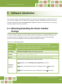
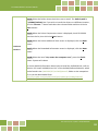
PCI-2602U Series Board User Manual Multi-function Boards Version 1.2, Mar. 2015 SUPPORT This manual relates to the following board: PCI-2602U WARRANTY All products manufactured by ICP DAS are warranted against defective materials for a period of one year from the date of delivery to the original purchaser. WARNING ICP DAS assumes no liability for damages consequent to the use of this product. ICP DAS reserves the right to change this manual at any time without notice. The information furnished by ICP DAS is believed to be accurate and reliable. However, no responsibility is assumed by ICP DAS for its use, nor for any infringements of patents or other rights of third parties resulting from its use. COPYRIGHT Copyright © 2014 by ICP DAS. All rights are reserved. TRADEMARKS Names are used for identification purposes only and may be registered trademarks of their respective companies. CONTACT US If you have any questions, feel to contact us by email at: [email protected] or [email protected] 1 PCI-2602U Multi-Function Boards TABLE OF CONTENTS Packing List ................................................................................................................................ 4 Related Information................................................................................................................... 4 1. 2. 3. Introduction ..................................................................................................................... 5 1.1. General Description ............................................................................................................... 5 1.2. Features ................................................................................................................................. 6 1.3. Specifications ......................................................................................................................... 7 1.4. Applications ........................................................................................................................... 8 Hardware Configuration .................................................................................................... 9 2.1. Board Layout.......................................................................................................................... 9 2.2. Jumper/Programmable Setting........................................................................................... 10 2.2.1. JP1 EEPROM Write Protection ....................................................................................................... 10 2.2.2. Card ID Switch ............................................................................................................................... 10 2.2.3. Analog Input Type Settings .............................................................................................................11 2.2.4. Digital Input/Output Mode Settings .............................................................................................. 12 2.3. System Block Diagram ......................................................................................................... 13 2.4. Analog Input Signal Connections ........................................................................................ 14 2.5. Analog Output Signal Connections ..................................................................................... 19 2.6. Pin Assignments .................................................................................................................. 20 Operation ......................................................................................................................... 22 3.1. AD Operation ....................................................................................................................... 22 3.2. DI/O Operation .................................................................................................................... 25 3.3. CON1 I/O Operation ............................................................................................................ 26 4. Hardware Installation...................................................................................................... 27 5. Software Installation ....................................................................................................... 31 5.1 Obtaining/Installing the Driver Installer Package ......................................................... 31 5.2 PnP Driver Installation ........................................................................................................ 33 User Manual/Ver. 1.2/Mar. 2015/PMH-0028 2 PCI-2602U Multi-Function Boards 5.3 6. 7. 5.3.1 Accessing Windows Device Manager ............................................................................................ 35 5.3.2 Check the Installation .................................................................................................................... 37 Testing the PCI-2602U Board ........................................................................................... 38 6.1 Self-Test Wiring.................................................................................................................... 38 6.2 Execute the Test Program .................................................................................................... 39 I/O Register Addresses..................................................................................................... 42 7.1. Determining the I/O Address using DOS ............................................................................ 42 7.2. The I/O Address Map .......................................................................................................... 44 7.3. Bar 1 (PLX)............................................................................................................................ 46 7.3.1 7.4. 8. 9. Verifying the Installation ..................................................................................................... 35 PLX Control/Status Registers ......................................................................................................... 46 Bar 3 (MMIO) ....................................................................................................................... 47 7.4.1 Interrupt and Initialize Control/Status Registers ........................................................................... 47 7.4.2 Digital I/O Registers ....................................................................................................................... 50 7.4.3 Analog Input Registers................................................................................................................... 52 7.4.4 Analog output registers ................................................................................................................. 55 Calibration........................................................................................................................ 57 8.1. Introduction ......................................................................................................................... 57 8.2. Step-by-Step Calibration Process ........................................................................................ 58 PCI-2602U Windows API Function .................................................................................. 59 Appendix: Daughter Boards .................................................................................................... 60 A1. DN-68A .................................................................................................................................................. 60 User Manual/Ver. 1.2/Mar. 2015/PMH-0028 3 PCI-2602U Multi-Function Boards Packing List The shipping package contains the following items: One multi-function board: PCI-2602U Series One printed Quick Start Guide One software utility CD Note: If any of these items are missing or damaged, contact the dealer from whom you purchased the product. Save the shipping materials and carton in case you need to ship or store the product in the future. Related Information Product Page: http://www.icpdas.com/root/product/solutions/pc_based_io_board/pci/pci-2602.html Documentation and Software for the UniDAQ SDK: CD:\NAPDOS\PCI\UniDAQ\ http://ftp.icpdas.com/pub/cd/iocard/pci/napdos/pci/unidaq/ User Manual/Ver. 1.2/Mar. 2015/PMH-0028 4 PCI-2602U Multi-Function Boards 1. Introduction The PCI-2602U board provides 1MHz 16/8-channel 16-bit Analog Input, 2-channel 16-bit Analog Output with 32-channel programmable Digital Input/Output 1.1. General Description The PCI-2602U is a powerful multifunction board that features a 1MS/s sampling rate and a 16-bit resolution converter that is suitable for the majority of industrial applications. The PCI-2602U board includes a universal PCI interface that supports both the 3.3 V and the 5V PCI bus, and features a continuous, 1MS/s 16-bit high resolution AD converter, 8 k Sample hardware AD FIFO, 2-channel 16-bit DA converter, 32-channel programmable Digital Input/Output and Digital Output Readback. The PCI-2602U also provides either 16 single-ended or 8 differential jumperless Analog Input channels and is equipped with a high-speed PGA featuring programmable gain controls. The PCI-2602U provides five programmable trigger methods including software-trigger, Post-trigger, Middle-trigger, Pre_trigger and Delay_trigger. The AD channel scan function of the PCI-2602U is called “MagicScan”, and removes most of the work required in acquiring AD values, such as selecting the channel, setting the gain and setting time, triggering the ADC and acquiring the data. With the built-in MagicScan function and the interrupt features of the PCI-2602U, the CPU in the Host system is effectively released from resource-heavy the data acquisition tasks. Even in channel scan mode, different gain code can be implemented for each channel, and the sampling rate can still reach a total of 1MS/s. The PCI-2602U also includes an onboard Card ID switch that can be used to set a unique ID for each board so that they can be instantly recognized if two or more PCI-2602U boards are installed in the same computer. If the Digital Input channels are disconnected, the status of the Digital Input will remain in Low instead of floating. User Manual/Ver. 1.2/Mar. 2015/PMH-0028 5 PCI-2602U Multi-Function Boards 1.2. Features The following is an overview of the general features provided by the PCI-2602U series board. Refer to Section 1.3 for more details. Interface Universal PCI (3.3 V/5 V) 2-channel bus mastering scatter/gather DMA Card ID switch Auto-calibration function Analog Input One 16-bit AD converter with maximum of 1M Samples/second 16 single-ended or 8 differential programmable Analog Inputs channels Multiple AD trigger methods Programmable gain and offset control On board 8192-sample AD FIFO Analog Output One DA converter 2-channel 16-bit voltage output Voltage output range: +/-10 V, +/-5 V, 0 ~ +10 V, 0 ~ +5 V On board 512-sample DA FIFO No bus loading in repetitive waveform generation applications Digital Input/Output On board 512-sample DO FIFO 32-channel programmable DI/O (4 x 8-channel). Digital Output readback function Programmable input digital filter for all Digital Input signals No bus loading in repetitive 8-bit digital pattern generation applications User Manual/Ver. 1.2/Mar. 2015/PMH-0028 6 PCI-2602U Multi-Function Boards 1.3. Specifications Model PCI-2602U Analog Input Channels 16 single-ended/8 differential A/D Converter 16-bit, 1 µs conversion time Sampling Rate 1 MS/s FIFO Size 8192 samples Over voltage Protection Continuous +/-35 Vp-p Input Impedance 10,000 MΩ/4pF Trigger Modes Software, Pacer, External Data Transfer Polling, Interrupt, DMA Accuracy 0.05 % of FSR ±1 LSB @ 25 °C, ± 10.24 V Input Range Gain: 0.4, 0.8, 1.6 Bipolar Range: ±10.24 V, ±5.12 V, ±2.56 V, Analog Output Channels 2 Resolution 16-bit Accuracy ± 6 LSB Output Range ±5 V, ±10 V, 0 ~ 10 V, 0 ~ 5 V, ±EXT_REF, 0~EXT_REF Output Driving +/- 5 mA Slew Rate 8.33 V/µs Output Impedance 0.1 Ω (Max.) Operating Mode Static update, Waveform generation (only for Channel 0) Output Rate 20 MS/s (Max.) FIFO Size 512 samples Programmable I/O Channels 32(4 port programmable) Digital Input Compatibility 5 V/TTL Input Voltage Logic 0: 0.8 V (Max.)/Logic 1: 2.0 V (Min.) Response Speed 1.0 MHz (Typical) Trigger Mode Software Data Transfer Polling User Manual/Ver. 1.2/Mar. 2015/PMH-0028 7 PCI-2602U Multi-Function Boards Digital Output Compatibility 5 V/CMOS Output Voltage Logic 0: 0.4 V (max.)/Logic 1: 2.4 V (min.) Output Capability Sink: 6 mA @ 0.33 V/Source: 6 mA @ 4.77 V DO Readback Yes Operation Mode Static update, Waveform generation Response Speed 4.0 MHz (Typical) DO Sample Clock frequency 10 MHz General Bus Type 3.3 V/5 V Universal PCI, 32-bit Data Bus 16-bit Card ID Yes (4-bit) I/O Connector SCSI 68-pin Dimensions (L x W x D) 149 mm x 102 mm x 22 mm Power Consumption 1 A @ +5 V (Max.) Operating Temperature 0 ~ 60 °C Storage Temperature -20 ~ 70 °C Humidity 5 ~ 85% RH, Non-condensing 1.4. Applications Signal Analysis FFT and Frequency Analysis Transient Analysis Temperature Monitor Vibration Analysis Energy Management Other Industrial and Laboratory Measurement and Control User Manual/Ver. 1.2/Mar. 2015/PMH-0028 8 PCI-2602U Multi-Function Boards 2. Hardware Configuration 2.1. Board Layout SW1 TP1 TP2 TP3 CON1 TB1 JP1 : : : : : : : DIP Switch used to configure the Board ID AGND for AD Calibration, Green 10 V for AD Calibration, Red 5 V for AD Calibration, Yellow I/O Signals (Sync_I, Sync_O) used Board Synchronization EEPROM Write Protection User Manual/Ver. 1.2/Mar. 2015/PMH-0028 9 PCI-2602U Multi-Function Boards 2.2. Jumper/Programmable Setting 2.2.1. JP1 EEPROM Write Protection Jumper JP1 is used to select the EEPROM Write Protection settings. When the jumper is set to the WRTIE PROTECT (LOCK) position (default), no data can be written to the EEPROM. To allow data to be written to the EEPROM, set JP1 to the UNLOCK position, as illustrated in the diagram below. EEPROM Write Protection Selection (JP1) JP1 JP1 EEPROM WRITE PROTECT EEPROM WRITE PROTECT LOCK EEPROM (Default) UNLOCK EEPROM 2.2.2. Card ID Switch The PCI-2602U includes an onboard Card ID switch (SW1) that enables the board to be recognized via software if two or more PCI-2602U boards are installed in the same computer. The default Card ID is 0x0. For more details regarding the SW1 Card ID settings, refer to the table below. Table 2.1 (*) Default Settings; OFF 1; ON 0 3 ID2 ON ON ON ON OFF OFF OFF OFF ON ON ON ON OFF OFF OFF OFF 4 ID3 ON ON ON ON ON ON ON ON OFF OFF OFF OFF OFF OFF OFF OFF NO SW1 ID 2 ID 3 2 ID1 ON ON OFF OFF ON ON OFF OFF ON ON OFF OFF ON ON OFF OFF ID 1 1 ID0 ON OFF ON OFF ON OFF ON OFF ON OFF ON OFF ON OFF ON OFF ID 0 Card ID (Hex) (*) 0x0 0x1 0x2 0x3 0x4 0x5 0x6 0x7 0x8 0x9 0xA 0xB 0xC 0xD 0xE 0xF 1 2 3 4 (Default Settings) User Manual/Ver. 1.2/Mar. 2015/PMH-0028 10 PCI-2602U Multi-Function Boards 2.2.3. Analog Input Type Settings The Analog Input type can be selected as either single-ended or differential. An example of the configuration is illustrated in the figure below. Note that before the Analog Input type settings, you must complete the hardware and software installation. Refer to Chapter 4 Hardware Installation and Chapter 5 Software Installation for more detailed information. Step 1: Open the Windows Device Manager. Step 2: Expand the DAQ Card item, and right-click the name of the PCI-2602U. Step 3: Select the Properties item from the popup menu. Step 4: In the Properties dialog, click the Advanced tap. Step 5: In the Analog Input Type section, select the Differential or Single Ended depending on your requirements. 1 2 3 4 5 User Manual/Ver. 1.2/Mar. 2015/PMH-0028 11 PCI-2602U Multi-Function Boards 2.2.4. Digital Input/Output Mode Settings The Digital Input/Output mode can be selected as either Digital Input or Digital Output depending on the specific configuration requirements. An example of the configuration is illustrated in the figure below. Note that before the Digital Input/Output mode settings, you must complete the hardware and driver installation. Refer to Chapter 4 Hardware Installation and Chapter 5 Software Installation for more detailed information. Step 1: Open the Windows Device Manager. Step 2: Expand the DAQ Card item, and right-click the name of the PCI-2602U. Step 3: Select the Properties item from the popup menu. Step 4: In the Properties dialog, click the Advanced tap. Step 5: In the PA/PB/PC/PD Digital I/O Mode sections, select the Digital Output or Digital Input depending on your requirements. 1 2 4 3 5 User Manual/Ver. 1.2/Mar. 2015/PMH-0028 12 PCI-2602U Multi-Function Boards 2.3. System Block Diagram The following is the block diagram for the PCI-2602: PCI Bus PCI Interface EEPROM (Calibration) Sync_O FIFO DI:512 K DO:512 K Sync_I Trigger Control Local System Controller Ext_Trg 32-ch DI/O DAC OUT 0 FIFO 512 K 2-ch, 16-bit DAC DAC OUT 1 MagicScan Controller FIFO 8K 16-bit ADC Gain MUX . . . User Manual/Ver. 1.2/Mar. 2015/PMH-0028 13 PCI-2602U Multi-Function Boards 2.4. Analog Input Signal Connections The PCI-2602U can be used to measure either single-ended or differential type Analog Input signals. Although certain signals can be measured using either mode, others, however, can only be measured in one mode or the other, and the most suitable mode for the measurement must be determined beforehand. In general, there are four different methods that can be used for connecting Analog Input signals, which are shown below in Figures 2.4-1 to 2.4-5. The connection method depicted in Figure 2.4-1 is suitable for grounding source Analog Input signals. The connection method depicted in Figure 2.4-3 is used to measure more channels than that shown in Figure 2.4-1, but is only suitable for large Analog Input signals. The connection method shown in Figure 2.4-4 is suitable for thermocouple input signals, and the connection method illustrated in Figure 2.4-5 is suitable for floating source Analog Input signals. Warning: As shown in Figure 2.4-4, the maximum common mode voltage between the Analog Input source and the AGND pin is 70 Vp-p, so care must be taken to ensure that the input signal is below this level before continuing. If the common mode voltage is set to above 70 Vp-p, the input multiplexer will be permanently damaged. The easiest way of determining the most suitable configuration method for the input signal connection is as follows. No. Type Connection Method 1 Grounding the source input signal See Figure 2.4-1 2 Thermocouple input signal See Figure 2.4-4 3 Floating source input signal See Figure 2.4-5 4 If the Vin is > 1 V and the gain is <= 10 V, and more channels are needed See Figure 2.4-3 5 Current source input signal See Figure 2.4-6 If thecharacteristics of the input signal are unknown or unclear, test the signal using the following procedure: 1. Test the signal using the connection method illustrated in Figure 2.4-1 and record the result 2. Test the signal using the connected method illustrated in Figure 2.4-4 and record the result 3. Test the signal using the connected method illustrated in Figure 2.4-5 and record the result 4. Compare the three results and select the most suitable connection User Manual/Ver. 1.2/Mar. 2015/PMH-0028 14 PCI-2602U Multi-Function Boards Figure 2.4-1 Connecting to the grounding source input (correct method) AI0 + PCI-2602U Es 1 S Es n S Es 1 S Es n S AI0 AI_GND AIn + AIn AI_GND Figure 2.4-2 Ground loop input (incorrect method) AI0 + PCI-2602U AI0 AI_GND AIn + AIn AI_GND User Manual/Ver. 1.2/Mar. 2015/PMH-0028 15 PCI-2602U Multi-Function Boards Figure 2.4-3 Connecting to single-ended input configuration AI0 AI1 AIn Es AI_GND Figure 2.4-4 Connecting to a thermocouple input configuration AI0 + AI0 - Ain + Ain AI_GND Do not join LO to AI_GND at the computer Note: If the input is not a thermocouple signal, an oscilloscope, rather than a voltage meter or multimeter, should be used to measure the common mode voltage of the Vin before connecting to the PCI-2602U. CAUTION: For the connection method shown in Figure 2.4-4, the maximum common mode voltage between the Analog Input source and the AGND pin is 70 Vp-p, so ensure that the input signal is below this value before continuing. If the common mode voltage is above 70 Vp-p, the input multiplexer will be permanently damaged. User Manual/Ver. 1.2/Mar. 2015/PMH-0028 16 PCI-2602U Multi-Function Boards Figure 2.4-5 Connecting to a floating source configuration AI CH 0 HI PCI-2602U Es 1 AI CH 0 LO A.GND 100 kΩ ~ 10 MΩ AI CH n HI Es n 100 kΩ ~ 10 MΩ AI CH n LO A.GND Figure 2.4-6 Connecting to a 4 ~ 20 mA Source AI CHn + R (Shunt Resistor) AGND - Example: A 20 mA source current through a 125 Ω resistor (e.g. 125 Ω, 0.1% DIP Resistors) between + and – terminals and the board will read a 2.5 VDC voltage. You can use the I = V/R (Ohm’s law) to calculate what value the source current should have. Current (I) = Voltage (V) / Resistance (R) = 2.5 V / 125 Ω = 0.02 A = 20 m User Manual/Ver. 1.2/Mar. 2015/PMH-0028 17 PCI-2602U Multi-Function Boards Signal Shielding The signal shielding connections methods in Figures 2.4-1to 2.4-6 are all the same Use a single-point connection to the frame ground, rather than the AI_GND, AO_GND or D_GND pins Vin PCI-2602U AI_GND AO_GND D_GND Frame Ground User Manual/Ver. 1.2/Mar. 2015/PMH-0028 18 PCI-2602U Multi-Function Boards 2.5. Analog Output Signal Connections The PCI-2602U board provides two DA output channels, AO0 and AO1, and the onboard -5 V (-10 V) reference signal on the PCI-2602U may be used to generate a DA output range of 0 V to +5 V (+10 V). A DA output range may also be created through the external reference signal AOx_REF, where the external reference input range is +/-10 V. For example, connecting to an external reference signal of +8 V will generate a DA output of 0 to +8 V. Figure 2.5-1 Connecting to an Analog Output channel for use as an internal reference signal (Recommended) Internal Referenc e AO0_OU DAC T Load (+/-5mA) PCI-2602U AO_GND Figure 2.5-2 Connecting to an Analog Output channel for use as an external reference signal Internal Reference AO0_REF AO0_OUT DAC Load PCI-2602U + External Reference - AO_GND User Manual/Ver. 1.2/Mar. 2015/PMH-0028 19 PCI-2602U Multi-Function Boards 2.6. Pin Assignments Note: AI0 ~ AI15: Single-ended (AI0+,AI0-) ~ (AI14+,AI14-) : Differential User Manual/Ver. 1.2/Mar. 2015/PMH-0028 20 PCI-2602U Multi-Function Boards Description of the I/O Connector Signals AI0 ~ AI15 AI0+ ~ AI7+ AI0- ~ AI7- AI_GND Input Analog Input channels 0 - 15. Each channel pair, AIx+, AIx- (x = 0, 2 … 14), can be configured as either two single-ended inputs or one differential input. AI_GND - - Analog Input Ground. AO_GND Input Analog Output channels 0 and 1. AO_GND Output External Reference for Analog Output channel 0 and 1. AO_GND - - Analog Output Ground. PA0 ~ PA7 PB0 ~ PB7 PC0 ~ PC7 PD0 ~ PD7 D_GND Input Output Digital Input/Output channels. D_GND - - Digital Ground Cnt0_CLK D_GND Input Clock Input for Counter0, which can be either an external or an internal source, as set using software. Cnt0_OUT D_GND Output Counter0 Output. Cnt0_GATE D_GND Input Counter0 Gate Control. AO0_OUT AO1_OUT AO0_REF AO1_REF Pacer_OUT D_GND Output Pacer Clock Output. This pin generates one pulse for each pacer clock when turned on. If the AD conversion is in pacer trigger mode, this signal can be used as a synchronous signal for other applications. Trg_GATE D_GND Input AD External Trigger Gate. When the Trg_GATE pin is connected to the DGND pin, it will disable the external trigger signal to the input. Ext_TRG D_GND Input AD External Trigger. +12 V D_GND Output +12 VDC Source. +5 V D_GND Output +5 VDC Source User Manual/Ver. 1.2/Mar. 2015/PMH-0028 21 PCI-2602U Multi-Function Boards 3. Operation 3.1. AD Operation The following is the block diagram for the AD system: CON1 IN0 SingleEnded Differential Buffer PGA ADC Polling Interrupt FIFO DMA Memory IN15 Software Trigger Ext_Trg SYNC_ I Post-Trigger Middle-Trigger Pre-Trigger Delay-Trigger Pacer Clock Software Clock MagicScan Controller TB1 Either the Ext_Trg or the Sync_I trigger signal is used to initiate a sequence of AD operations. If the Software Trigger is used, the AD operations will be initiated without using the Ext_Trg or the Sync_I signals. User Manual/Ver. 1.2/Mar. 2015/PMH-0028 22 PCI-2602U Multi-Function Boards The following is an overview of the five trigger modes: Trigger Mode Software-trigger Post-trigger Middle-trigger Pre-trigger Delay-trigger Description No trigger signal is used and all AD operations are initiated using software. Either the Ext_Trg or the Sync_I trigger signal is used to initiate the AD operations. Either the Ext_Trg or the Sync_I trigger signal is used to indicate the middle of the AD operations. Either the Ext_Trg or the Sync_I trigger signal is used to indicate the end of the AD operations. Either the Ext_Trg or the Sync_I trigger signal is used to start the delay timer that is used to initiate the AD operations. The only difference between a Post-trigger and the Delay-trigger is the inclusion of the delay timer. User Manual/Ver. 1.2/Mar. 2015/PMH-0028 23 PCI-2602U Multi-Function Boards After the clock signal is generated, AD data will be recorded and saved to the buffer or the FIFO. Two clock sources are provided, a software clock and a pacer clock. The saved data can be transferred to the memory on the PC using either software polling, Interrupt transfer or DMA transfer. Different combinations of trigger mode, clock signal and data transfer can be used to create four different types of AD applications, which are summarized below: Clock Mode Transfer Mode FIFO (K Samples) Trigger Source Software Trigger Software Polling N/A N/A Software Trigger Post-Trigger Middle-Trigger Pre-Trigger Delay-Trigger Pacer Clock Polling 8 Ext_Trg Sync_I Software Trigger Post-Trigger Delay-Trigger Pacer Clock Interrupt 8 Ext_Trg Sync_I Software-Trigger Post-Trigger Delay-Trigger Pacer Clock DMA 8 Ext_Trg Sync_I Trigger Mode Notes: The Ext_Trg source is Pin2 on CON1. Refer to Section 2.6 for details. The Sync_I source is Pin1 of TB1. Refer to Section 2.1 for details. User Manual/Ver. 1.2/Mar. 2015/PMH-0028 24 PCI-2602U Multi-Function Boards 3.2. DI/O Operation Four groups are provided on the PCI-2602U board, PA, PB, PC and PD, and each group consists of 8 channels. When the system is first switched on, all groups are configured as Digital Input. A custom program can be used to independently re-configure each of the four groups as either Digital Input or Digital Output, meaning that read operations from Digital Output group will acquire Digital Output values, but write operations to the Digital Input group will not do anything. A digital filter is also provided for all Digital Input ports. When the PA group is set to output mode, a digital pattern can be continuously generated on a Digital Output port using a user-defined data pattern and data rate that is based on 100 ns high-resolution timing. PD Group PC Group PB Group PA Group User Manual/Ver. 1.2/Mar. 2015/PMH-0028 25 PCI-2602U Multi-Function Boards 3.3. CON1 I/O Operation The Counter0 pin on the CON1 connector can be used as either an event counter or a pulse output. The designed as a Board Synchronization Interface. The block diagram for the CK0 Event Counter is illustrated below: The block diagram for the Counter0 Pulse Output is illustrated below: User Manual/Ver. 1.2/Mar. 2015/PMH-0028 26 PCI-2602U Multi-Function Boards 4. Hardware Installation Note: It is recommended that the driver is installed before installing the hardware as the computer may need to be restarted once the driver is installed in certain operating systems, such as Windows 2000 or Windows XP, etc. Installing the driver first helps reduce the time required for installation and restarting the computer. To install PCI-2602U board, follow the procedure described below: Step 1: Install the driver for the PCI-2602U card on your computer. For detailed information about the driver installation, refer to Chapter 5 Software Installation. Step 2: Configure the Card ID using the DIP-Switch (SW1). For detailed information about the card ID, refer to Section 2.2.2 Card ID Switch. User Manual/Ver. 1.2/Mar. 2015/PMH-0028 27 PCI-2602U Multi-Function Boards Step 3: Shut down and switch off the power to the computer, and then disconnect the power supply. Step 4: Remove the cover from the computer. Step 5: Select an empty PCI slot. User Manual/Ver. 1.2/Mar. 2015/PMH-0028 28 PCI-2602U Multi-Function Boards Step 6: Unscrew and remove the PCI slot cover from the computer case. Step 7: Remove the connector cover from the PCI-2602U. Step 8: Carefully insert the PCI-2602U card into the PCI slot by gently pushing down on both sides of the card until it slides into the PCI connector. User Manual/Ver. 1.2/Mar. 2015/PMH-0028 29 PCI-2602U Multi-Function Boards Step 9: Confirm that the card is correctly inserted in the motherboard, and then secure the PCI-2602U card in place using the retaining screw that was removed in Step 6. Step 10: Replace the covers on the computer. Step 11: Re-attach any cables, insert the power cord and the switch one the power to the computer. Once the computer reboots, follow any message prompts that may be displayed to complete the Plug and Play installation procedure, refer to Chapter 5 Software Installation. User Manual/Ver. 1.2/Mar. 2015/PMH-0028 30 PCI-2602U Multi-Function Boards 5. Software Installation This chapter provides a detailed description of the process for installing the PCI-2602U driver and how to verify whether the PCI-2602U was properly installed. PCI-2602U card can be used on Windows 2000 and 32-/64-bit XP/2003/2008/Vista/7/8 based systems, and the drivers are fully Plug and Play compliant for easy installation. 5.1 Obtaining/Installing the Driver Installer Package The driver installer package for the PCI-2602U card can be found on the supplied CD-ROM, or can be obtained from the ICP DAS FTP web site. Install the appropriate driver for your operating system. The location and addresses are indicated in the Table5.1-1 below. Table 5.1-1: UniDAQ Driver/SDK Operating System Windows 2000, 32/64-bit Windows XP, 32/64-bit Windows 2003, 32/64-bit Windows 2008, 32/64-bit Windows Vista, 32/64-bit Windows 7, 32/64-bit Windows 2008, 32/64-bit Windows 8 Driver Name UniDAQ Driver/SDK (unidaq_win_setup_xxxx.exe) CD-ROM CD:\\ NAPDOS\PCI\UniDAQ\DLL\Driver\ Web site http://ftp.icpdas.com/pub/cd/iocard/pci/napdos/pci/unidaq/dll/driver/ Please follow the following steps to setup software: Step 1: Double click the UniDAQ_Win_Steupxxx.exe to setup it. Installation Procedure Step 2: When the Setup Wizard screen is displayed, click the Next> button. Step 3: When the Information screen is displayed, click the Next> button. User Manual/Ver. 1.2/Mar. 2015/PMH-0028 31 PCI-2602U Multi-Function Boards Step 4: Select the folder where the drivers are to install. The default path is C:\ICPDAS\UniDAQ. But if you wish to install the drivers to a different location , click the “Browse…” button and select the relevant folder and then click the Next> button. Step 5: When the Select Components screen is displayed, check PCI-2602U board on the list, then click the Next> button. Step 6: When the Select Additional Tasks screen is displayed, click the Next> button. Installation Procedure Step 7: When the Download Information screen is displayed, click the Next> button. Step 8: Select the item “Yes, restart the computer now”, press the Finish button. System will reboot. For more detailed information about how to install the UniDAQ driver, refer to “Section 2.2 Install UniDAQ Driver DLL” of the UniDAQ Software Manual, which can be found in the \NAPDOS\PCI\UniDAQ\Manual\ folder on the companion CD, or can be downloaded from: http://ftp.icpdas.com/pub/cd/iocard/pci/napdos/pci/unidaq/manual/ User Manual/Ver. 1.2/Mar. 2015/PMH-0028 32 PCI-2602U Multi-Function Boards 5.2 PnP Driver Installation Step 1: Correctly shut down and power off your computer and disconnect the power supply, and then install the PCI-2602U into the computer. For detailed information about the hardware installation of the PCI-2602U, refer to Chapter 4 Hardware Installation. Step 2: Power on the computer and complete the Plug and Play installation. Note: More recent operating systems, such as Windows Vista/7/8 will automatically detect the new hardware and install the necessary drivers etc., so Steps 3 to 5 can be skipped. Step 3: Select “Install the software automatically [Recommended]” and click the “Next>” button. User Manual/Ver. 1.2/Mar. 2015/PMH-0028 33 PCI-2602U Multi-Function Boards Step 4: Click the “Finish” button. Step 5: Windows pops up “Found New Hardware” dialog box again. User Manual/Ver. 1.2/Mar. 2015/PMH-0028 34 PCI-2602U Multi-Function Boards 5.3 Verifying the Installation To verify that the driver was correctly installed, use the Windows Device Manager to view and update the device drivers installed on the computer, and to ensure that the hardware is operating correctly. The following is a description of how access the Device Manager in each of the major versions of Windows. Refer to the appropriate description for your the operating system to verify the installation. 5.3.1 Accessing Windows Device Manager Windows 2000/XP Step 1: Click the “Start” button and then point to “Settings” and click “Control Panel”. Double-click the “System” icon to open the “System Properties” dialog box. Step 2: Click the “Hardware” tab and then click the “Device Manager” button. Windows Server 2003/2008 Step 1: Click the “Start” button and point to “Administrative Tools”, and then click “Computer Management” option. Step 2: Expand the “System Tools” item in the console tree, and then click “Device Manager”. User Manual/Ver. 1.2/Mar. 2015/PMH-0028 35 PCI-2602U Multi-Function Boards Windows Vista/7 Step 1: Click “Start” button. Step 2: In the Search field, type Device Manager and the press Enter. Note that Administrator privileges are required for this operation. If you are prompted for an administrator password or confirmation, enter the password or provide confirmation by clicking the “Yes” button in the User Account Control message. Windows 8 Step 1: To display the Start screen icon from the desktop view, hover the mouse cursor over the bottom-left corner of screen. Step 2: Right-click the Start screen icon and then click “Device Manager”. Alternatively, press [Windows Key] +[X] to open the Start Menu, and than select Device Manager from the options list. Right-click User Manual/Ver. 1.2/Mar. 2015/PMH-0028 36 PCI-2602U Multi-Function Boards 5.3.2 Check the Installation Check the PCI-2602U card which listed correctly or not, as illustrated below. Installation successful User Manual/Ver. 1.2/Mar. 2015/PMH-0028 37 PCI-2602U Multi-Function Boards 6. Testing the PCI-2602U Board This chapter provides detailed information about the “Self-Test” process, which is used to confirm that PCI-2602U board operating correctly. Before beginning the “Self-Test” process, ensure that both the hardware and driver installation procedures are fully completed. For detailed information about the hardware and driver installation, refer to Chapter 4 Hardware Installation and Chapter 5 Software Installation. 6.1 Self-Test Wiring Preparing the device: Before beginning the “Self-Test” procedure, ensure that the following items are available: A CA-SCSI15-H (optional) cable A DN-68A (optional) terminal board Step 1: Connect the DN-68A to the CON1 connector on the board using the CA-SCSI15-H cable. User Manual/Ver. 1.2/Mar. 2015/PMH-0028 38 PCI-2602U Multi-Function Boards Analog Input/Output Test Wiring: Step 2: Open the advanced configuration tool in the Windows Device Manager to configuration the Analog Input type for Single-Ended input, refer to section 2.2.3 Analog Input Type Setting for more detail information. Step 3: Connect the AO0_Out (Pin58) to AI0 (Pin68), and connect the AI_GND (Pin60) to AO_GND (Pin57). 6.2 Execute the Test Program After installation, the UniDAQ Utility will be located in the default folder (C:\ICPDAS\UniDAQ\Driver\). Use the procedure described below to perform the “Self-Test”. Step 1: In Windows XP, click the “Start” button, point to “All Programs” and then click the “ICPDAS” folder. Point to “UniDAQ Development Kits” and then click “UniDAQ Utility”. 2 3 Step 2: Confirm that the PCI-2602U board has been successfully installed in the Host system. Note that device numbers start from 0. Step 3: Click the “TEST” button to start the test. User Manual/Ver. 1.2/Mar. 2015/PMH-0028 39 PCI-2602U Multi-Function Boards Step 4: Check the results of the Analog Input/Output functions test result. 1. Click the “Analog Output” tab. 2. Select the “0” from the “Channel” drop-down menu. 3. Select the “1: Bipolar +/- 5V” from the “Range” drop-down menu. 4. Enter the voltage value depending on your requirements (e.g. 4) in the “Voltage(V)” field. 5. Click the “OUTPUT” button to output voltage. User Manual/Ver. 1.2/Mar. 2015/PMH-0028 40 PCI-2602U Multi-Function Boards 6. Click the “Analog Input” tab. 7. Confirm the configuration setting. 8. Click the “Start” button. 9. Check Analog Input on Channel 0 textbox. The other channels value for floating number. Complete User Manual/Ver. 1.2/Mar. 2015/PMH-0028 41 PCI-2602U Multi-Function Boards 7. I/O Register Addresses 7.1. Determining the I/O Address using DOS The Plug&Play BIOS will assign an appropriate I/O address for each installed PCI-2602U board during the power-on stage. Each card includes four fixed ID numbers which are indicated below: Model Name PCI-2602U Vendor ID 0x10B5 Device ID 0x9054 Sub Vendor ID 0x3577 Sub Device ID 0x2602 The following functions are provided: 1. P2602_DriverInit(&wTotalBoards) This function can be used to detect how many PCI-2602U cards are installed in the system, and is implemented based on the PCI Plug & Play mechanism. The function also records the I/O resources information for each card and stores the details in the library. Usage examples: wTotalBoards =1 There is only one PCI-2602U board installed in this system. wTotalBoards =2 There are two PCI-2602U boards installed in this system. 2. P2602_GetConfigAddressSpace(wBoardNo, *wBaseAddr, *wIrqNo, *wBasePLX, *dwBaseAddr) This function is used to read the I/O resource information for a PCI-2602U board installed in the system. The application will then be able to directly control all of the functions related to the PCI-2602U board. wBoardNo=0 to N : There are a total N+1 PCI-2602U boards of wBaseAddr wBaseAddr, wBasePLX, dwBaseAddr : The base address of the PCI-2602U board wIrq : the IRQ channel number allocated to this PCI-2602U board User Manual/Ver. 1.2/Mar. 2015/PMH-0028 42 PCI-2602U Multi-Function Boards The following is a sample of the source code for use with DOS: // Step1: Detect all PCI-2602U cards first wRetVal=P2602_DriverInit(&wTotalBoards); printf("There are %d PCI-2602U Cards in this PC\n",wBoards); // Step2: Save resource of all PCI-2602U cards installed in this PC for (wBoardNo=0; i<wBoards; i++) { P2602_GetConfigAddressSpace(i, &wBaseAddr[wBoardNo], &wIrqNo[wBoardNo], &wBasePLX[wBoardNo], &dwBaseAddr[wBoardNo], ); printf("\nCard%d: wBase=%x, wIrq=%x, wBasePLX=%x,dwBaseAddr = %lx", , wBoardNo[wBoardNo] ,wBaseAddr[wBoardNo] ,wIrqNo[wBoardNo] ,wBasePLX[wBoardNo] ,dwBaseAddr[wBoardNo]); } // Step3: Control the PCI-2602U directly // write the DIO states of card0 mem4g_write_dword(dwBaseAddr[0] +0x214,dwDoValue); // read the DIO states of card0 dwDiValue= mem4g_read_dword(dwBaseAddr[0] +0x214); // write the DIO states of card1 mem4g_write_dword(dwBaseAddr[1] +0x214,wDoValue); // read the DIO states of card1 wDiValue= mem4g_read_dword(wBaseDIO+0x0); User Manual/Ver. 1.2/Mar. 2015/PMH-0028 43 PCI-2602U Multi-Function Boards 7.2. The I/O Address Map An overview of the registers for the PCI-2602U board is given below. The address of each register can be determined by simply adding the offset value to the base address of the corresponding Bar number. More detailed descriptions of each register can be found in the following. Bar No. Offset Register Function Description Read Write PLX Interrupt Control/Status PLX Interrupt Control/Status DMA Control/Status DMA Control/Status 200H Initialize Control/Status Hardware Status 204H Interrupt Control/Status Interrupt Control/Status 208H EEPROM Control/Status EEPROM Control/Status 20CH EEPROM Control/Status EEPROM Control/Status 210H DIO Mode Control/Status DIO Mode Control/Status 214H Read DIO Port Write DIO Port 218H Read DI FIFO Data N/A 21CH DI FIFO Status N/A 220H DO Pattern Output Control/Status DO Pattern Output Control/Status 22CH AI Scan Mode Control/Status AI Scan Mode Control/Status 230H Time Tick Status(ms) N/A 234H Time Tick Status(us) N/A 238H CNT0 Clock Control/Status CNT0 Clock Control/Status 23CH Delay Trigger Clock Control/Status Delay Trigger Clock Control/Status 240H DI Filter Clock Control/Status DI Filter Clock Control/Status 244H AI Internal Clock Control/Status AI Internal Clock Control/Status 248H DI Internal Clock Control/Status DI Internal Clock Control/Status 24CH DO Internal Clock Control/Status DO Internal Clock Control/Status 250H AO0 Internal Clock Control/Status AO0 Internal Clock Control/Status 254H AO1 Interrupt Clock Control/Status AO1 Interrupt Clock Control/Status 258H Internal Clock Control N/A 68H 1 80H (PLX) ∣ B8H 3 (MMIO) User Manual/Ver. 1.2/Mar. 2015/PMH-0028 44 PCI-2602U Multi-Function Boards Bar No. Offset 280H 3 (MMIO) Register Function Description Read Write AI External Analog Trigger Control/Status AI External Analog Trigger Control/Status 290H AI Trigger Mode Control/Status AI Trigger Mode Control/Status 294H AI Software Trigger Status AI Software Trigger Control 298H AI Scan Address AI Scan Address 2ECH AI Configuration Control/Status AI Configuration Control/Status 2F0H Save AI Configuration N/A 2A0H Read AI FIFO Data N/A 2A4H AI FIFO Status N/A 2A8H AI Data Acquisition Size AI Data Acquisition Size 2ACH AI Data Acquisition Start AI Data Acquisition Start 2B0H AO Configuration Control/Status AO Configuration Control/Status 2B4H Write AO Channel 0 Data Write AO Channel 0 Data 2B8H Write AO Channel 1 Data Write AO Channel 1 Data 2BCH AO Pattern Output Control/Status AO Pattern Output Control/Status 2C4H Connector I/O Control/Status Connector I/O Control/Status Note: The length of the register is 32-bits. User Manual/Ver. 1.2/Mar. 2015/PMH-0028 45 PCI-2602U Multi-Function Boards 7.3. Bar 1 (PLX) 7.3.1 PLX Control/Status Registers (Read/Write)wBase+0x68 Read/Write interrupt Control/Status For more detailed information, refer to the documentation for the PLX9054, which can be found at: http://www.plxtech.com/products/io/pci9054#technicaldocumentation (Write)wBase+0x80 ~ 0xB8 Read/Write DMA Control/Status For more detailed information, refer to the documentation for the PLX9054, which can be found at: http://www.plxtech.com/products/io/pci9054#technicaldocumentation User Manual/Ver. 1.2/Mar. 2015/PMH-0028 46 PCI-2602U Multi-Function Boards 7.4. Bar 3 (MMIO) 7.4.1 Interrupt and Initialize Control/Status Registers Register 7.4.1-1wBase+0x200 Initialize Control/Status Bit Description Write 0 Reset AI Mode. Write a 1 and Write a 0 to resets AI Mode. Yes 1 Clear AI FIFO. Write a 1 and Write a 0 to clear AI FIFO. Yes 2 Reset AI FIFO Overflow Status. Write a 1 and Write a 0 to resets AI FIFO over flow status. Yes 3 PCI Clear Interrupt. Write a 1 and Write a 0 to clear PCI interrupts. Yes Reserved. Yes 6 DI(PC) FIFO Reset. Write a 1 and Write a 0 to resets digital input FIFO. Yes 7 DO(PA) FIFO Reset. Write a 1 and Write a 0 to resets digital output FIFO. Yes 8 AO0 FIFO Reset. Write a 1 and Write a 0 to resets analog output channel 0 FIFO. Yes Reserved. No 4:5 9:31 Register 7.4.1-2 wBase+0x200 Hardware Status Bit Description Read 0:3 Card ID. Reading a data indicates a Card ID of SW1. Yes 4:7 Reserved. PA DIO Mode. Reading a 1 indicates a PA is DO mode. Reading a 0 indicates a PA is DI mode. PB DIO Mode. Reading a 1 indicates a PB is DO mode. Reading a 0 indicates a PB is DI mode. PC DIO Mode. Reading a 1 indicates a PC is DO mode. Reading a 0 indicates a PC is DI mode. Yes 8 9 10 11 12:31 Yes Yes Yes PD DIO Mode. Reading a 1 indicates a PD is DO mode. Reading a 0 indicates a PD is DI mode. Yes Reserved. Yes User Manual/Ver. 1.2/Mar. 2015/PMH-0028 47 PCI-2602U Multi-Function Boards Register 7.4.1-3 wBase+0x204 Interrupt Clear/Status Bit 0 1 2 3 4 5 6 7 8 9 10 11 12:31 Description AI Pacer Done Int. Reading a 1 indicates an analog input pacer is complete. Reading a 0 indicates a pacer is not complete. Write a 1 and write a 0 to clear AI Pacer Down interrupt. AI FIFO Half-Full Int. Reading a 1 indicates an analog input FIFO status is half-full. Reading a 0 indicates an analog input FIFO status is not half-full. Write a 1 and write a 0 to clear AI FIFO Half-Full interrupt. AI FIFO Full Int. Reading a 1 indicates an analog input FIFO status is full. Reading a 0 indicates an analog input FIFO status is not full. Write a 1 and write a 0 to clear AI FIFO FULL interrupt. DI Pacer Done Int. Reading a 1 indicates a digital input pacer is complete. Reading a 0 indicates a digital pacer is not complete. Write a 1 and write a 0 to clear DI Pacer Down interrupt. DI(PC) FIFO Half-Full Int. Reading a 1 indicates a digital input FIFO status is half-full. Reading a 0 indicates a digital input FIFO status is not half-full. Write a 1 and write a 0 to clear DI FIFO Half-Full interrupt. DI(PC) FIFO Full Int. Reading a 1 indicates a digital input FIFO status is full. Reading a 0 indicates a digital input FIFO status is not full. Write a 1 and write a 0 to clear DI FIFO FULL interrupt. AO0 Pattern Done Int. Reading a 1 indicates a AO0 Pattern output is complete. Reading a 0 indicates a AO0 Pattern output is not complete. Write a 1 and write a 0 to clear AO0 Pattern Done interrupt. DO(PA) Pattern Done Int. Reading a 1 indicates a DO(PA) Pattern output is complete. Reading a 0 indicates a PA Pattern output is not complete. Write a 1 and write a 0 to clear PA Pattern Done interrupt. External Trigger Int. Reading a 1 indicates an external trigger status is ready. Reading a 0 indicates an external trigger status is not ready. Write a 1 and write a 0 to clear external trigger interrupt. SYNC_I Trigger Int. Analog Trigger Int. Reading a 1 indicates an analog trigger status is ready. Reading a 0 indicates an analog trigger status is not ready. Write a 1 and write a 0 to clear analog trigger interrupt. Counter Int. Reading a 1 indicates an Counter Interrupt status is ready. Reading a 0 indicates an analog trigger status is not ready. Write a 1 and write a 0 to clear analog trigger interrupt. Reserved. Read Write Yes Yes Yes Yes Yes Yes Yes Yes Yes Yes Yes Yes Yes Yes Yes Yes Yes Yes Yes Yes Yes Yes Yes Yes Yes No User Manual/Ver. 1.2/Mar. 2015/PMH-0028 48 PCI-2602U Multi-Function Boards Register 7.4.1-4 wBase+0x224 Interrupt Mode Control/Status Bit 0 1 2 3 4 5 6 7 8 9 10 11 12:31 Description Enable AI Pacer Done Interrupt. Write a 1 enables interrupt when analog input pacer is done. Enable AI FIFO Half-Full Interrupt. Write a 1 enables interrupt when analog input FIFO is half-full. Enable AI FIFO Full Interrupt. Write a 1 enables interrupt when analog input FIFO is full. Enable DI(PC) Pacer Done Interrupt. Write a 1 enables digital input interrupt when pacer done. Enable DI(PC) FIFO Half-Full Interrupt. Write a 1 enables digital input FIFO half-full interrupt. Enable DI(PC) FIFO Full Interrupt. Write a 1 enables digital input FIFO full interrupt. Enable AO0 Pattern Done Interrupt. Write a 1 enables AO0 pattern down interrupt. Enable DO(PA) Pattern Done Interrupt. Write a 1 enables PA pattern down interrupt. Enable External Trigger Interrupt. Write a 1 enables external trigger interrupt. Enable SYNC_I Trigger Interrupt. Enable Analog Trigger Interrupt. Write a 1 enables analog trigger interrupt. Enable Timer Interrupt. Reserved. Read Write Yes Yes Yes Yes Yes Yes Yes Yes Yes Yes Yes Yes Yes Yes Yes Yes Yes Yes Yes Yes Yes Yes Yes Yes Yes No User Manual/Ver. 1.2/Mar. 2015/PMH-0028 49 PCI-2602U Multi-Function Boards 7.4.2 Digital I/O Registers Register 7.4.2-1 wBase+0x210 DIO Mode Control/Status Bit 0 1 2 3 4 5 6 7 8:10 11:13 14 15:31 Description PA DIO Mode. Write a 1 indicates a PA is DO mode. Write a 0 indicates a PA is DI mode. PB DIO Mode. Write a 1 indicates a PB is DO mode. Write a 0 indicates a PB is DI mode. PC DIO Mode. Write a 1 indicates a PC is DO mode. Write a 0 indicates a PC is DI mode. PD DIO Mode. Write a 1 indicates a PD is DO mode. Write a 0 indicates a PD is DI mode. Enable PA Digital Input Filter. Write a 1 enables digital input filter. Enable PB Digital Input Filter. Write a 1 enables digital input filter. Enable PC Digital Input Filter. Write a 1 enables digital input filter. Enable PD Digital Input Filter. Write a 1 enables digital input filter. DI Clk Select. Write a 100 enables digital output clock. DO Clk Select. Write a 101 enables digital output clock. PA Output Mode. Writing a 1 indicates the PA output mode is pattern mode. Writing a 0 indicates the PA output mode is static mode. Reserved. Read Write Yes Yes Yes Yes Yes Yes Yes Yes Yes Yes Yes Yes Yes Yes Yes Yes Yes Yes Yes Yes Yes Yes Yes No Read Write Yes Yes Yes Yes Yes Yes Yes Yes Register 7.4.2-2 wBase+0x214 Write DIO Port Bit 0:7 8:15 16:23 24:31 Description PA Write. Write the digital output data to specified digital I/O Port-PA, When PA is digital output mode. PB Write. Write the digital output data to specified digital I/O Port-PB, When PB is digital output mode. PC Write. Write the digital output data to specified digital I/O Port-PC, When PC is digital output mode. PD Write. Write the digital output data to specified digital I/O Port-PD, When PD is digital output mode. User Manual/Ver. 1.2/Mar. 2015/PMH-0028 50 PCI-2602U Multi-Function Boards Register 7.4.2-3 wBase+0x214 Read DIO Port Bit 0:7 8:15 16:23 24:31 Description PA Read. Read the digital input data to specified digital I/O Port-PA, When PA is digital input mode. PB Read. Read the digital input data to specified digital I/O Port-PB, When PB is digital input mode. PC Read. Read the digital input data to specified digital I/O Port-PC, When PC is digital input mode. PD Read. Read the digital input data to specified digital I/O Port-PD, When PD is digital input mode. Read Yes Yes Yes Yes Register 7.4.2-4 wBase+0x218 Read DI FIFO Data Bit 0:7 8:31 Description FIFO Read. Read the digital input data to specified FIFO. Reserved. Read Yes Yes Register 7.4.2-5 wBase+0x21C DI FIFO Status Bit 0:15 16 17 18 19 20 21 22:31 Description Read Yes Yes Yes Yes Yes Yes Yes Yes Reserved. FIFO Empty. Reading a 1 indicates a FIFO status is empty. FIFO Full. Reading a 1 indicates a FIFO status is full. FIFO Half Full. Reading a 1 indicates a FIFO status is half-full. FIFO Almost Full. Reading a 1 indicates a FIFO status is almost full. FIFO Almost Empty. Reading a 1 indicates a FIFO status is almost empty. FIFO Overflow. Reading a 1 indicates a FIFO status is overflow. Reserved. Register 7.4.2-6 wBase+0x220 DO Pattern Control/Status Bit 0:10 11:15 16:31 Description DO(PA) Data Num. Write value indicates the waveform points for PA. DO(PA) Cycle Num. Write 0~30 indicates the PA is burst mode, the write n indicates to generate n+1 pulse. Write 31 indicates the PA output mode is continuous mode. Reserved Read Yes Write Yes Yes Yes Yes No User Manual/Ver. 1.2/Mar. 2015/PMH-0028 51 PCI-2602U Multi-Function Boards 7.4.3 Analog Input Registers Register 7.4.3-1 wBase+0x22C AI Scan Mode Control/Status Bit Read Write Enable AI Scan. Writing a 1 enables MagicScan Mode to scan analog input channel. Yes Yes 1:16 Total Scan Channel Number. Indicates the number of channels to MagicScan. Writing a N indicates an N+1 channels. Ex. Writing a 14 indicates 15 channels. Writing an 8 indicates 9 channels. Yes Yes 17:31 Reserved. Yes No Read Write Yes Yes Yes Yes Yes No Read Write Yes Yes 0 Description Register 7.4.3-2 wBase+0x244 AI Internal Clock Control/Status Bit 0:23 24:25 26:31 Description Set Div Clock. Indicates the (WORD)((Base Clock/Sampling Rate)-1) to set internal pacer clock during an analog input operation. Select Base Clock. Writing 00 indicates 40MHz. Writing 01 indicates 10M. Writing 10 indicates 1MHz. Writing 11 indicates 100KHz. Reserved. Register 7.4.3-3 wBase+0x290 AI Trigger Mode Control/Status Bit 0:2 Description Clock Source. Writing 000 indicates a non-clock source. Writing 001 indicates a Single Clk. Writing 010 indicates a T3 Clk. Writing 101 indicates an external clock source. 3:4 Trigger Source. Writing 00 indicates an external trigger. Writing 01 indicates an Sync_I. Yes Yes 5:7 Trigger Mode. Writing 000 indicates an internal trigger mode. Writing 001 indicates a post-trigger mode. Writing 010 indicates a middle-trigger mode. Writing 011 indicates a pre-trigger mode. Writing 100 indicates a delay-trigger mode. Writing 101 indicates a analog-trigger mode. Yes Yes Yes Yes Yes Yes Yes No 8 9:11 12:31 Enable Analog Trigger. Writing a 1 enables analog trigger mode to acquire the analog data when an external analog signal start. Analog Trigger Type. Writing 000 disable analog trigger mode. Writing 001 enable a above-high. Writing 010 enable a below-low. Writing 011 enable inside-region (V2<AD<V1). Writing 100 enable an outside-region (AD>V1, AD<V2). Reserved. User Manual/Ver. 1.2/Mar. 2015/PMH-0028 52 PCI-2602U Multi-Function Boards Register 7.4.3-4 wBase+0x294 AI Software Trigger Control Bit 0 1:31 Description Software Trigger Start. Writing a 0 causes the analog input channel to measure analog input data. Reserved. Read Write No Yes Yes No Read Yes Write No Yes No Yes No Read Write No Yes Yes No Write Yes Yes Yes Yes Register 7.4.3-5 wBase+0x294 AI Software Trigger Status Bit 0:15 16 17:31 Description Software Trigger Data Read. Read the analog input data. Trigger Status. Reading a 1 indicates a Trigger Status is ready. Reading a 0 indicates a Trigger Status is busy. Reserved. Register 7.4.3-6 wBase+0x298 AI Scan Address Bit 0:15 16:31 Description AI Scan Address Register. Indicates the scan sequence number during a MagicScan operation. Reserved. Register 7.4.3-7 wBase+0x2EC AI Configuration Control/Status Bit 0 1 2 3 1 0 1 1 Read Yes Yes Yes Yes 4 5 0 0 Yes Yes Yes Yes 1 Analog Input Range (Gain). 1 Analog Input Type. Writing a 1 indicates a signal-ended type. Writing a 0 indicates a differential type. Channel Select 0. Writing a 1 indicates an odd channel. Writing a 0 indicates an even channel. Reserved. Yes Yes Yes Yes Yes Yes Yes Yes Yes Yes Yes No Reserved. 1 Channel Select 1. Indicates value to use analog input channel number div 2. Reserved. Yes Yes No Yes No Yes Yes No 6 7:9 10 11 12 13 14 15 16:18 19:31 Description User Manual/Ver. 1.2/Mar. 2015/PMH-0028 53 PCI-2602U Multi-Function Boards Register 7.4.3-8 wBase+0x2F0 Save AI Configuration Data Bit 0 1:31 Description Save AI Configuration Data. Writing a 0 indicates to save configuration data. Reserved. Read Write Yes Yes Yes No Register 7.4.3-9 wBase+0x2A0 Read AI FIFO Data Bit 0:15 16:31 Description FIFO Read. Read the analog input data to specified FIFO. Reserved. Read Yes Yes Register 7.4.3-10 wBase+0x2A4 AI FIFO and Trigger Status Bit 0:15 16 17 18 19 20 21 22 23 24 25 26 27 28:31 Description Read Yes Yes Yes Yes Yes Yes Yes Yes Yes Yes Yes Yes Yes Yes Reserved. FIFO Empty. Reading a 1 indicates a FIFO status is empty. FIFO Full. Reading a 1 indicates a FIFO status is full. FIFO Half Full. Reading a 1 indicates a FIFO status is half-full. FIFO Almost Full. Reading a 1 indicates a FIFO status is almost full. FIFO Almost Empty. Reading a 1 indicates a FIFO status is almost empty. FIFO Overflow. Reading a 1 indicates a FIFO status is overflow. Trigger In. Post Trigger. Analog Trigger Ready Analog Trigger V1A5 Analog Trigger V2A5 Analog Trigger Fit Reserved. Register 7.4.3-11 wBase+0x2A8 AI Data Acquisition Size Bit 0:31 Description Data Acquisition Size. Indicates the number to acquire data during an analog input operation. Writing an 8000000 acquires analog input data continuous. Read Write Yes Yes Read Write Yes Yes Register 7.4.3-12 wBase+0x2AC AI Data Acquisition Start Bit 0:31 Description Acquisition Start. Writing a 0 to causes channel to start acquisition data if AI Data Acquisition Size register is set. User Manual/Ver. 1.2/Mar. 2015/PMH-0028 54 PCI-2602U Multi-Function Boards 7.4.4 Analog output registers Register 7.4.4-1 wBase+0x2B0 AO Configuration Control/Status Bit Description Read Write 0 Channel 0 Enable. Writing a 1 enables channel to output data. Writing a 0 disables the channel. Yes Yes 1 Channel 0 Polar. Writing a 1 indicates the channel 0 polar is uni-polar. Writing a 0 indicates the channel 0 polar is Bi-polar. Yes Yes Yes Yes Yes Yes Yes Yes Yes Yes Yes Yes Yes Yes Yes Yes Yes Yes Yes Yes Yes Yes Yes No 2 3 4 5 6 7 Channel 0 Internal Ref. Writing a 1 indicates the channel 0 internal reference is 5V.Writing a 0 indicates the channel 0 internal reference is 10V. Channel 0 Reference Mode. Writing a 1 indicates the channel 0 is internal reference. Writing a 0 indicates the channel 0 is external reference. Channel 1 Enable. Writing a 1 enables channel to output data. Writing a 0 disables the channel. Channel 1 Polar. Writing a 1 indicates the channel 1 polar is uni-polar. Writing a 0 indicates the channel 1 polar is Bi-polar. Channel 1 Internal Ref. Writing a 1 indicates the channel 1 internal reference is 5V.Writing a 0 indicates the channel 1 internal reference is 10V. Channel 1 Reference Mode. Writing a 1 indicates the channel 1 is internal reference. Writing a 0 indicates the channel 1 is external reference. 10:12 Channel 0 Output Mode. Writing a 1 indicates the channel 0 output mode is pattern mode. Writing a 0 indicates the channel 0 output mode is static mode. Channel 1 Output Mode. Writing a 1 indicates the channel 1 output mode is pattern mode. Writing a 0 indicates the channel 1 output mode is static mode. Channel 0 Clk Select. Write a 110 enables analog output channel 0 clock. 13:15 16:31 Channel 1 Clk Select. Write a 111 enables analog output channel 1 clock. Reserved. 8 9 User Manual/Ver. 1.2/Mar. 2015/PMH-0028 55 PCI-2602U Multi-Function Boards Register 7.4.4-2 wBase+0x2B4 Write AO Channel 0 Data Bit 0:15 16:31 Description AO Channel 0 Write. Writing the analog output data to channel 0. Reserved. Read Write Yes Yes Yes Yes Read Write Yes Yes Yes Yes Read Write Yes Yes Yes Yes Yes No Register 7.4.4-3 wBase+0x2B8 Write AO Channel 1 Data Bit 0:15 16:31 Description AO Channel 1 Write. Read the analog output data to channel 1. Reserved. Register 7.4.4-4 wBase+0x2BC AO Pattern Output Control/Status Bit 0:10 11:15 16:31 Description AO Channel 0 Data Num. Write value indicates the waveform points for channel 0. AO Channel 0 Cycle Num. Write 0~30 indicates the channel 0 is burst mode, the write n indicates to generate n+1 pulse. Write 31 indicates the channel 0 output mode is continuous mode. Reserved User Manual/Ver. 1.2/Mar. 2015/PMH-0028 56 PCI-2602U Multi-Function Boards 8. Calibration 8.1. Introduction When shipped from the factory, the PCI-2602U board is already fully calibrated, including the calibration coefficients that are stored in the onboard EEPROM. For a more precise application of voltages in the field, the procedure described below provides a method that allows the board installed in a specific system to be calibrated so that the correct voltages can be achieved for the field connection. This calibration allows the effects of voltage drops caused by IR loss in the cable and/or the connector to be eliminated. At first the user has to prepare the equipment for calibration: the precise multi-meter. Note that the calibrated values for analog output/input channels are stored within 3 words in the address of the EEPROM, as shown in the table below. The calibration procedure will be described in detail in the Section 8.2. The calibration values stored in the EEPROM are as follows: EEPROM Address Bipolar Uipolar Bipolar Unipolar +5V +0V +10V +0V +5V -5V +10V -10V EEPROM Address Reference Calibration 10V 5V 4:5 6:7 DA Calibration CH 0 CH 1 8 16 9 17 10 18 11 19 12 20 13 21 14 22 15 23 EEPROM Address Bipolar 10.24V Bipolar 5.12V Bipolar 2.56V Bipolar 1.28V Bipolar 0.64V Bipolar 20.48 10V Ref 0V 5V Ref 0V 2.54V 0V 1.27V 0V 0.63V 0V 10V Ref 0V AD Calibration AD CH0 24 25 28 29 32 33 36 37 40 41 48 49 User Manual/Ver. 1.2/Mar. 2015/PMH-0028 57 PCI-2602U Multi-Function Boards 8.2. Step-by-Step Calibration Process The following is a step-by-step description of the calibration process using the Windows Calibration Program for the PCI-2602U, which can be downloaded form: http://ftp.icpdas.com/pub/cd/iocard/pci/napdos/pci/pci-2602/dll/calibration/ Connect a voltage meter to the (TP2, TP1) pins to acquire the 10V Ref value. 2 1 Connect a voltage meter to the (TP3, TP1) pins to acquire the 5V Ref value. 3 Move the jumper for JP1 from pins 1/2 to pins 2/3 to enable EEPROM write operations. 4 6 5 Step1. Analog Output Calibration 7 Enter the 10V reference value in the 10V Ref(TP2) field in the voltage reference section. utility. Enter the 5V reference value in the 5V Ref(TP3) filed in the voltage reference section. Click the START button to begin the calibration process. Once the calibration process is complete, click the SAVE button to save calibration to the board. User Manual/Ver. 1.2/Mar. 2015/PMH-0028 58 PCI-2602U Multi-Function Boards 9. PCI-2602U Windows API Function For more details regarding the Windows API Functions for the PCI-2602U board, refer to UniDAQ SDK User manual, which can be downloaded from: CD:\NAPDOS\PCI\UniDAQ\Manuql http://ftp.icpdas.com/pub/cd/iocard/pci/napdos/pci/unidaq/manual/ User Manual/Ver. 1.2/Mar. 2015/PMH-0028 59 PCI-2602U Multi-Function Boards Appendix: Daughter Boards A1. DN-68A The DN-68A is a general-purpose DIN-Rail mountable daughter board containing female 68 pin D-sub I/O Connectors and is designed to allow easy field wiring connections. 68-Pin cable CON1 DN-68A PCI-2602U Pins 01 to 68 on the DN-68A daughter board are connected to the CON1 connector on the PCI-2602U using a 68-pin male-male cable. The FG on the DN-68A is connected to the shielding wire of the 68-pin cable. User Manual/Ver. 1.2/Mar. 2015/PMH-0028 60