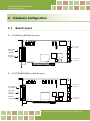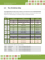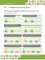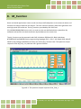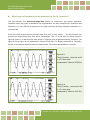
1
PCI-1202/1602/180x Series Card User Manual Multi-Function Boards Version 4.8, Mar. 2015 SUPPORTS Board includes PEX-1202L, PEX-1202H, PCI-1202L, PCI-1202H, PCI-1202LU, PCI-1202HU, PCI-1602, PCI-602F, PCI-1602U, PCI-1602FU, PCI-1800L, PCI-1800H, PCI-1800LU, PCI-1800HU, PCI-1802L, PCI-1802H, PCI-1802LU and PCI-1802HU. WARRANTY All products manufactured by ICP DAS are warranted against defective materials for a period of one year from the date of delivery to the original purchaser. WARNING ICP DAS assumes no liability for damages consequent to the use of this product. ICP DAS reserves the right to change this manual at any time without notice. The information furnished by ICP DAS is believed to be accurate and reliable. However, no responsibility is assumed by ICP DAS for its use, nor for any infringements of patents or other rights of third parties resulting from its use. COPYRIGHT Copyright © 2013 by ICP DAS. All rights are reserved. TRADEMARK Names are used for identification only and may be registered trademarks of their respective companies. CONTACT US If you have any question, please feel to contact us. We will give you quick response within 2 workdays. Email: [email protected], [email protected] PCI-1202/1602/180x Series Card Multi-Function Boards TABLE OF CONTENTS PACKING LIST ................................................................................................................................................................ 5 RELATED INFORMATION ............................................................................................................................................... 5 1. INTRODUCTION ................................................................................................................................................. 6 1.1 FEATURES ............................................................................................................................................................ 8 1.2 THE BLOCK DIAGRAM .......................................................................................................................................... 11 1.3 SPECIFICATIONS .................................................................................................................................................. 12 1.3.1 PEX-1202/PCI-1202 Series................................................................................................................................. 12 1.3.2 PCI-1602 Series ................................................................................................................................................. 14 1.3.3 PCI-1800/PCI-1802 Series ................................................................................................................................. 16 2. HARDWARE CONFIGURATION ...........................................................................................................................18 2.1 BOARD L AYOUT .................................................................................................................................................. 18 2.2 JUMPER SETTING ................................................................................................................................................ 21 2.2.1 JP1: A/D Input Type Selection ...................................................................................................................... 21 2.2.2 J1: D/A Reference Voltage Selection ............................................................................................................ 22 2.2.3 D/I Port Setting (Pull-High/Low) .................................................................................................................. 22 2.3 CARD ID SWITCH ................................................................................................................................................ 23 2.4 ANALOG INPUT SIGNAL CONNECTION...................................................................................................................... 24 2.5 PIN ASSIGNMENTS............................................................................................................................................... 29 3. HARDWARE INSTALLATION ...............................................................................................................................32 4. SOFTWARE INSTALLATION ................................................................................................................................36 4.1 DRIVER INSTALLING PROCEDURE............................................................................................................................. 36 4.2 PNP DRIVER INSTALLATION ................................................................................................................................... 38 4.3 CONFIRM THE SUCCESSFUL INSTALLATION ................................................................................................................ 41 5. TESTING PCI-1202/1602/180X CARD ...................................................................................................................42 5.1 SELF-TEST WIRING .............................................................................................................................................. 42 5.1.1 DIO Test Wiring ........................................................................................................................................... 42 5.1.2 Analog Input Test Wiring ............................................................................................................................. 43 5.1.3 Analog Output Test Wiring .......................................................................................................................... 44 5.2 EXECUTE THE TEST PROGRAM ................................................................................................................................ 46 User Manual/ Ver. 4.8/ Mar. 2015/ PMH-0014-48/ Page: 2 PCI-1202/1602/180x Series Card Multi-Function Boards 6. I/O CONTROL REGISTER ....................................................................................................................................50 6.1 HOW TO FIND THE I/O ADDRESS ............................................................................................................................ 50 6.2 THE ASSIGNMENT OF I/O ADDRESS ........................................................................................................................ 53 6.3 THE I/O ADDRESS MAP ....................................................................................................................................... 54 6.4 BAR1: TIMER CONTROL ....................................................................................................................................... 55 6.5 BAR2: CONTROL REGISTER ................................................................................................................................... 58 6.5.1 The Control Register .................................................................................................................................... 58 6.5.2 The Status Register ...................................................................................................................................... 79 6.5.3 The A/D Software Trigger Register .............................................................................................................. 80 6.6 BAR3: DI/DO REGISTER...................................................................................................................................... 81 6.6.1 Digital Output/Digital Input ........................................................................................................................ 81 6.6.2 Card ID Register ........................................................................................................................................... 82 6.7 7. BAR4: A/D AND D/A REGISTER ............................................................................................................................ 83 A/D CONVERSION OPERATION .........................................................................................................................86 7.1 THE CONFIGURATION CODE TABLE .......................................................................................................................... 86 7.2 THE UNIPOLAR/BIPOLAR ...................................................................................................................................... 87 7.3 THE INPUT SIGNAL RANGE .................................................................................................................................... 87 7.4 THE SETTLING TIME ............................................................................................................................................. 88 7.5 WHEN TO DELAY THE SETTLING TIME ...................................................................................................................... 88 7.6 THE AD CONVERSION MODE ................................................................................................................................ 89 7.7 THE FIXED-CHANNEL MODE AD CONVERSION .......................................................................................................... 91 7.8 THE MAGICSCAN MODE AD CONVERSION............................................................................................................... 92 7.8.1 The MagicScan Circular_Scan_Queue ......................................................................................................... 93 7.8.2 The Digital Filter of MagicScan ................................................................................................................... 94 7.8.3 The Digital Filter of MagicScan ................................................................................................................... 94 7.8.4 The High/Low Alarm of MagicScan ............................................................................................................. 95 7.8.5 The MagicScan Function.............................................................................................................................. 95 7.8.6 The MagicScan Thread ................................................................................................................................ 98 8. M_FUNCTION .................................................................................................................................................100 8.1 9. INTRODUCTION ................................................................................................................................................. 101 CONTINUOUS CAPTURE FUNCTION ................................................................................................................105 9.1 GENERAL PURPOSE FUNCTIONS ........................................................................................................................... 105 9.2 FUNCTIONS FOR SAVING DATA IN PC MEMORY ....................................................................................................... 109 10. 10.1 CALIBRATION .............................................................................................................................................110 A/D CALIBRATION ............................................................................................................................................. 110 User Manual/ Ver. 4.8/ Mar. 2015/ PMH-0014-48/ Page: 3 PCI-1202/1602/180x Series Card Multi-Function Boards 10.2 11. D/A CALIBRATION ............................................................................................................................................. 112 DEMO PROGRAM .......................................................................................................................................114 11.1 DEMO PROGRAM FOR WINDOWS ........................................................................................................................ 114 11.2 DIAGNOSTIC PROGRAM ...................................................................................................................................... 117 12. 11.2.1 Power-on Plug&Play Test ......................................................................................................................... 117 11.2.2 Driver Plug&Play Test .............................................................................................................................. 117 11.2.3 D/O Test ................................................................................................................................................... 118 11.2.4 D/A Test ................................................................................................................................................... 118 11.2.5 A/D Test ................................................................................................................................................... 118 PERFORMANCE EVALUATION .....................................................................................................................119 APPENDIX: DAUGHTER BOARD .................................................................................................................................. 120 A1. DB-37 and DN-37............................................................................................................................................... 120 A2. DB-8125............................................................................................................................................................. 120 A3. DB-8225............................................................................................................................................................. 121 A4. DB-16P Isolated Input Board ............................................................................................................................. 121 A5. DB-16R Relay Board .......................................................................................................................................... 122 A6. DB-24PR Power Relay Board ............................................................................................................................. 123 User Manual/ Ver. 4.8/ Mar. 2015/ PMH-0014-48/ Page: 4 PCI-1202/1602/180x Series Card Multi-Function Boards Packing List The shipping package includes the following items: One multi-function card as follows: PEX-1202 series: PEX-1202L/ PEX-1202H PCI-1202 series: PCI-1202L/ PC-1202H/ PCI-1202LU/ PCI-1202HU PCI-1602 series: PCI-1602/ PCI-1602F/ PCI-1602U/ PCI-1602FU PCI-1800 series: PCI-1800L/ PCI-1800H/ PCI-1800LU/ PCI-1800HU PCI-1802 series: PCI-1802L/ PCI-1802H/ PCI-1802LU/ PCI-1802HU One printed Quick Start Guide ★ Note!! One software utility CD One CA-4002 D-Sub Connect If any of these items is missing or damaged, contact the dealer from whom you purchased the product. Save the shipping materials and carton in case you want to ship or store the product in the future. Related Information Product Page: http://www.icpdas.com/root/product/solutions/pc_based_io_board/pci/pci-1202.html http://www.icpdas.com/root/product/solutions/pc_based_io_board/pci/pci-1602.html http://www.icpdas.com/root/product/solutions/pc_based_io_board/pci/pci-1800.html Documentation and Software for UniDAQ SDK: CD:\NAPDOS\PCI\UniDAQ\ http://ftp.icpdas.com/pub/cd/iocard/pci/napdos/pci/unidaq/ User Manual/ Ver. 4.8/ Mar. 2015/ PMH-0014-48/ Page: 5 PCI-1202/1602/180x Series Card Multi-Function Boards 1. Introduction Comparison Table Model Name PEX-1202L PCI-1202LU PEX-1202H PCI-1202HU PCI-1602U PCI-1602FU PCI-1800LU PCI-1800HU PCI-1802LU PCI-1802HU Bus D/A A/D Channel Channel PCI Express 12-bit, Universal 2-ch PCI PCI Express 12-bit, Universal 2-ch PCI Universal 12-bit, PCI 2-ch Universal 12-bit, PCI 2-ch Universal 12-bit, PCI 2-ch Universal 12-bit, PCI 2-ch Universal 12-bit, PCI 2-ch Universal 12-bit, PCI 2-ch A/D Software Sampling Trigger Rate (Polling) Pacer Scan (Magic Scan) Post-trigger Pre-trigger Middle-trigger FIFO Size 12-bit, 32 S.E./ 110 kS./s 1k 44 kS./s 1k 100 kS./s 8k 200 kS./s 8k 330 kS./s 1k 44 kS./s 1k 330 kS./s 8k 44 kS./s 8k 16 Diff. 12-bit, 32 S.E./ 16 Diff. 16-bit, 32 S.E./ 16 Diff. 16-bit, 32 S.E./ 16 Diff. 12-bit, 16 S.E./ 8 Diff. 12-bit, 16 S.E./ 8 Diff. 12-bit, 32 S.E./ 16 Diff. 12-bit, 32 S.E./ 16 Diff. User Manual/ Ver. 4.8/ Mar. 2015/ PMH-0014-48/ Page: 6 PCI-1202/1602/180x Series Card Multi-Function Boards General Description The PCI-1800/1802(L/H) series are high performance, multifunction analog, digital I/O board for PC and compatible computers in a 5 V PCI slot. This series features a continuous, 330 k Samples/Sec., gap-free data acquisition under DOS. This family has the same features: one 12-bit 330 k AD converter, two 12-bit independent DA converters, 16-channel TTL compatible DI and 16-channel TTL compatible DO. The PCI-1800 series provides 16 single-ended or 8 differential inputs. The PCI-1802 series provides 32 single-ended or 16 differential inputs. Two DACs of this multifunction card are independent bipolar voltage output with jumper selectable voltage output range. The AD scan function of 1800 series is very amazing; we call it “MagicScan”. It scans with two modes: the fixed-channel mode and the channel-scan mode, both modes can be up to 330 k samples per second. We also provide three trigger modes for this series: software trigger, pacer trigger and external trigger; each trigger mode uses “MagicScan” to perform the data acquisition. The external trigger can be programmed to one of the three trigger methods: pre-trigger, post-trigger and middle-trigger. The PEX-1202(L/H) is new version of PCI-1202 series card they can be installed in PCI Express bus. The PCI-1202/1800/1802(HU/LU) and PCI-1602(U/FU) are new version of PCI-1202/1800/1802(H/L) and PCI-1602(/F) they can be installed in 3.3 V, 5 V or 3.3 V/5 V Universal PCI-Bus. The PEX-1202(L/H), PCI-1202/1800/1802(H/L) and PCI-1602(/F) could be replaced with PCI-1202/1800/1802(HU/LU) and PCI-1602(U/FU) without modifying software. The PEX/PCI-1202 series is very similar to PCI-1802 series. The different items between the PCI-1802 and PEX/PCI-1202 are given as follows: * A/D sampling rate is 110 k Samples/Sec. for PEX-1202(L) and PCI-1202(L/LU) * FIFO size is 1 k samples The PCI-1602(/U/FU) is very similar to PCI-1802(L). The different items between the PCI-1802 and PCI-1602 are given as follows: * A/D is 16-bit * A/D sampling rate is 200 k Samples/Sec. for PCI-1602(F/FU) * A/D sampling rate is 100 k Samples/Sec. for PCI-1602(U) User Manual/ Ver. 4.8/ Mar. 2015/ PMH-0014-48/ Page: 7 PCI-1202/1602/180x Series Card Multi-Function Boards 1.1 Features Interface: Supports the +5 V PCI bus for PCI-1202/1800/1802(L/H) and PCI-1602(/F) series card. Supports the +3.3 V/+5 V PCI bus for PCI-1202/PCI-1800/PCI-1802(LU/HU) and PCI-1602(U/FU) series card. Supports PCI Express x 1 for PEX-1202(L/H) series card. Digital Input/Output: 16 channels TTL compatible D/I. 16 channels TTL compatible D/O. High Speed data transfer rate: refer to chapter 10. Analog Output: 2 channels 12-bit DACs. Bipolar voltage output with ±5 V or ± 10 V by jumper selectable. High throughput: refer to chapter 10. 12-bit DAC output code for PEX-1202(L/H) and PCI-1202/1800/1802(L/H/LU/HU). 12-bit DAC Output Code Data Input MSB Analog Output LSB 1111 1111 1111 +Vref (2047/2048) 1000 0000 0001 +Vref (1/2048) 1000 0000 0000 0 Volts 0001 1111 1111 -Vref (1/1024) 0000 0000 0000 -Vref (2048/2048) User Manual/ Ver. 4.8/ Mar. 2015/ PMH-0014-48/ Page: 8 PCI-1202/1602/180x Series Card Multi-Function Boards Analog Input: 32 S.E./ 16 Diff. analog inputs for PEX-1202 and PCI-1202/1602/1802 series card. 16 S.E./8 Diff. analog inputs for PCI-1800 series card. A/D converter = 12-bit, 330 k Samples/Sec. for PCI-1800/1802(L/LU). A/D converter = 12-bit, 110 k Samples/Sec. for PEX-1202(L) and PCI-1202(L/LU). A/D converter = 12-bit, 44 k Samples/Sec. for PEX-1202(H) and PCI-1202/1800/1802(H/HU). A/D converter = 16-bit, 200 k Samples/Sec. for PCI-1602(F/FU). A/D converter = 16-bit, 100 k Samples/Sec. for PCI-1602(/U). Programmable input signal configuration. Provides “MagicScan” function. FIFO Size: 1 k samples for PEX-1202(L/H) and PCI-1202/1800(L/H/LU/HU). 8 k samples for PCI-1602 (/F/U/FU) and PCI-1802(L/H/LU/HU). Three A/D trigger sources: software, Pacer and external trigger. Three external trigger modes: pre-trigger, middle-trigger and post-trigger. External trigger CHn CHn t t Start End Internal pacer trigger Start End External post-trigger External trigger External trigger CHn CHn N2 Start External middle-trigger End t t Start External End pre-trigger User Manual/ Ver. 4.8/ Mar. 2015/ PMH-0014-48/ Page: 9 PCI-1202/1602/180x Series Card Multi-Function Boards 12-bit ADC input voltages and output codes for PEX-1202 and PCI-1202/1800/1802 series. 12-bit ADC Input Voltages and Output Codes Analog Input Digital Output Binary Code Hex Code MSB LSB +9.995 V 1111 1111 1111 FFF +0 V 1000 0000 0000 800 -4.88 mV 0111 1111 1111 7FF -10 V 0000 0000 0000 000 16-bit ADC input voltages and output codes for PCI-1602 series. 16-bit ADC Input Voltages and Output Codes Analog Input Digital Output Binary Code Hex Code MSB LSB +9.99 V 0111 1111 1111 1111 7FFF +0 V 0000 0000 0000 0000 0000 -305 µV 1111 1111 1111 1111 FFFF -10 V 1000 0000 0000 0000 8000 Timer/Counter: Three 16-bit independent timers. Timer 0 is used as the internal A/D pacer trigger. Timer 1 is used as the external trigger. Timer 2 is used as the machine independent timer. User Manual/ Ver. 4.8/ Mar. 2015/ PMH-0014-48/ Page: 10 PCI-1202/1602/180x Series Card Multi-Function Boards 1.2 The Block Diagram The block diagram of the PEX-1202 and PCI-1202/1602/1800/1802 series card is given as follows: User Manual/ Ver. 4.8/ Mar. 2015/ PMH-0014-48/ Page: 11 PCI-1202/1602/180x Series Card Multi-Function Boards 1.3 Specifications 1.3.1 PEX-1202/PCI-1202 Series Model Name PEX-1202L PEX-1202H PCI-1202LU PCI-1202HU Channels Analog Input 32 single-ended / 16 differential A/D Converter Sampling Rate FIFO Size Over Voltage Protection Input Impedance Trigger Modes 12-bit, 8.5 µs conversion time 110 kS./s 44 kS./s 110 kS./s 44 kS./s 1024 samples Continuous ±35 Vp-p 10 MΩ/6 pF Software, Internal programmable pacer, External (5 V/TTL compatible) Data Transfer Accuracy Polling 0.01 % of FSR ±1 LSB @ 25 °C, ± 10 V Zero Drift ± 4 ppm/°C of FSR Analog Output Channels Resolution Accuracy Output Rang Output Driving Slew Rate 2-ch 12-bit 0.06% of FSR ± 1 LSB @ 25 °C, ± 10 V Bipolar: ±5 V, ±10 V ± 5 mA 8.33 V/µs Output Impedance Operating Mode 0.1 Ω max. Software Digital Input Channels 16-ch Compatibility Input Voltage 5 V/TTL Logic 0: 0.8 V max. / Logic 1: 2.0 V min. Response Speed 500 KHz 2.7 MHz (Typical) Digital Output Channels Compatibility 16-ch 5 V/CMOS 5 V/TTL Output Voltage Logic 0 0.1 V max. 0.4 V max. Logic 1 4.4 V min. 2.4 V min. Output Capability Sink 6 mA @ 0.33 V 2.4 mA @ 0.8 V Source 6 mA @ 4.77 V 0.8 mA @ 2.0 V 500 KHz 2.7 MHz (Typical) Response Speed User Manual/ Ver. 4.8/ Mar. 2015/ PMH-0014-48/ Page: 12 PCI-1202/1602/180x Series Card Multi-Function Boards Model Name PEX-1202L PEX-1202H PCI-1202LU PCI-1202HU Timer/Counter Channels 3 (Independent x 1/Internal pacer x 1/External pacer x 1) Resolution 16-bit Compatibility 5 V/TTL Input Frequency 10 MHz max. Reference Clock Internal: 8 MHz General Bus Type PCI Express x1 Data Bus 16-bit Card ID Yes (4-bit) I/O Connector 3.3V/5V Universal PCI, 32-bit, 33MHz Yes (4-bit) for Version 4.0 or above Female DB37 x 1, Male 20-bit ribbon x 2 Dimensions (L x W x D) 162 mm x 100 mm x 22 mm 195 mm x 97 mm x 22 mm Power Consumption 300 mA @ +5 V Operating Temperature 0 ~ 60 °C Storage Temperature -20 ~ 70 °C Humidity 5 ~ 85% RH, non-condensing Analog Input Range Model Name PEX-1202L/PCI-1202LU (Low-Gain) Gain 0.5 1 2 4 8 Bipolar (V) ± 10 ±5 ± 2.5 ± 1.25 ± 0.625 Unipolar (V) - 0 ~ 10 0~5 0 ~ 2.5 0 ~ 1.25 Sampling Rage Max. Model Name 110 kS./s PEX-1202H/PCI-1202HU (High-Gain) Gain 0.5 1 5 10 50 100 500 1000 Bipolar (V) ± 10 ±5 ±1 ± 0.5 ± 0.1 ± 0.05 ± 0.01 ± 0.005 Unipolar (V) - 0~10 - 0~1 - 0 ~ 0.1 - 0 ~ 0.01 Sampling Rate Max. 44 kS./s 10 kS./s 1 kS./s User Manual/ Ver. 4.8/ Mar. 2015/ PMH-0014-48/ Page: 13 PCI-1202/1602/180x Series Card Multi-Function Boards 1.3.2 PCI-1602 Series Model Name PCI-1602U PCI-1602FU PCI-1602 PCI-1602F Channels Analog Input 32 single-ended / 16 differential A/D Converter Sampling Rate 16-bit, 2 µs conversion time 100 kS./s 200 kS./s 100 kS./s 200 kS./s FIFO Size Over Voltage Protection 8192 samples Continuous ±35 Vp-p Input Impedance Trigger Modes Data Transfer Accuracy Zero Drift 10 MΩ/6 pF Software, Internal programmable pacer, External (5 V/TTL compatible) Polling 0.01 % of FSR ±1 LSB @ 25 °C, ± 10 V ± 2 ppm/°C of FSR Analog Output Channels Resolution 2-ch 12-bit Accuracy Output Rang 0.06% of FSR ± 1 LSB @ 25 °C, ± 10 V Bipolar: ±5 V, ±10 V Output Driving Slew Rate Output Impedance Operating Mode ± 5 mA 8.33 V/µs 0.1 Ω max. Software Digital Input Channels 16-ch Compatibility 5 V/TTL Logic 0: 0.8 V max. Logic 1: 2.0 V min. 2.7 MHz (Typical) Input Voltage Response Speed Digital Output Channels 16-ch Compatibility 5 V/TTL Logic 0: 0.4 V max. Logic 1: 2.4 V min. Output Voltage Output Capability Sink: 2.4 mA @ 0.8 V Source: 0.8 mA @ 2.0 V Response Speed 2.7 MHz (Typical) User Manual/ Ver. 4.8/ Mar. 2015/ PMH-0014-48/ Page: 14 PCI-1202/1602/180x Series Card Multi-Function Boards Model Name PCI-1602U PCI-1602FU PCI-1602 PCI-1602F Timer/Counter Channels 3 (Independent x 1/Internal pacer x 1/External pacer x 1) Resolution 16-bit Compatibility 5 V/TTL Input Frequency 10 MHz max. Reference Clock Internal: 8 MHz General Bus Type 3.3 V/5 V Universal PCI, Data Bus 16-bit Card ID Yes (4-bit) I/O Connector 5 V PCI bus, 32-bit, 33 MHz 32-bit, 33 MHz No Female DB37 x 1 Male 20-bit ribbon x 2 Dimensions (L x W x D) 188 mm x 105 mm x 22 mm Power Consumption 350 mA @ +5 V Operating Temperature 0 ~ 60 °C Storage Temperature -20 ~ 70 °C Humidity 5 ~ 85% RH, non-condensing Analog Input Range Model Name PCI-1602U/PCI-1602 Gain Bipolar (V) 1 2 4 8 ± 10 ±5 ± 2.5 ± 1.25 Sampling Rage Max. Model Name Gain Bipolar (V) Sampling Rate Max. 100 kS./s PCI-1602FU/PCI-1602F 1 2 4 8 ± 10 ±5 ± 2.5 ± 1.25 200 kS./s User Manual/ Ver. 4.8/ Mar. 2015/ PMH-0014-48/ Page: 15 PCI-1202/1602/180x Series Card Multi-Function Boards 1.3.3 PCI-1800/PCI-1802 Series Model Name FIFO Size PCI-1802H PCI-1802L Analog Input 32 single-ended / 16 differential 12-bit, 3 µs conversion time 330 kS./s for High Gain 44 kS./s for Low Gain 8192 samples Over Voltage Protection Input Impedance Continuous ±35 Vp-p 10 MΩ/6 pF Trigger Modes Data Transfer Software, Internal programmable pacer, External (5 V/TTL compatible) Polling Accuracy Zero Drift Channels Resolution Accuracy 0.01 % of FSR ±1 LSB @ 25 °C, ± 10 V ± 2 ppm/°C of FSR Analog Output 2-ch 12-bit 0.06% of FSR ± 1 LSB @ 25 °C, ± 10 V Output Rang Output Driving Bipolar: ±5 V, ±10 V ± 5 mA Slew Rate Output Impedance 8.33 V/µs 0.1 Ω max. Operating Mode Software Channels A/D Converter Sampling Rate PCI-1802HU PCI-1802LU PCI-1800HU PCI-1800LU PCI-1800H PCI-1800L 32 single-ended / 16 differential 1024 samples Digital Input Channels Compatibility 16-ch 5 V/TTL Input Voltage Logic 0: 0.8 V max. Logic 1: 2.0 V min. Response Speed 2.7 MHz (Typical) Digital Output Channels Compatibility 16-ch 5 V/TTL Output Voltage Logic 0: 0.4 V max. Logic 1: 2.4 V min. Output Capability Sink: 2.4 mA @ 0.8 V Source: 0.8 mA @ 2.0 V Response Speed 2.7 MHz (Typical) User Manual/ Ver. 4.8/ Mar. 2015/ PMH-0014-48/ Page: 16 PCI-1202/1602/180x Series Card Multi-Function Boards Model Name PCI-1802HU PCI-1802H PCI-1800HU PCI-1800H PCI-1802LU PCI-1802L PCI-1800LU PCI-1800L Timer/Counter Channels 3 (Independent x 1/Internal pacer x 1/External pacer x 1) Resolution 16-bit Compatibility 5 V/TTL Input Frequency 10 MHz max. Reference Clock Internal: 8 MHz General 3.3 V/5 V Bus Type Universal PCI, 16-bit Card ID Yes (4-bit) I/O Connector 5 V PCI bus, 32-bit, Universal PCI, 32-bit, 33 MHz 32-bit, 33 MHz Data Bus 3.3 V/5 V 5 V PCI bus, 33 MHz 32-bit, 33 MHz No Yes (4-bit) No Female DB37 x 1 Male 20-bit ribbon x 2 Dimensions (L x W x D) 200 mm x 105 mm x 22 mm Power Consumption 300 mA @ +5 V Operating Temperature 0 ~ 60 °C Storage Temperature -20 ~ 70 °C Humidity 5 ~ 85% RH, non-condensing Analog Input Range Model Name PCI-1802(L/LU)/PCI-1800(L/LU) (Low-Gain) Gain 0.5 1 2 4 8 Bipolar (V) ± 10 ±5 ± 2.5 ± 1.25 ± 0.625 Unipolar (V) - 0 ~ 10 0~5 0 ~ 2.5 0 ~ 1.25 Sampling Rage Max. Model Name 330 kS./s PCI-1802(H/HU)/PCI-1800(H/HU) (High-Gain) Gain 0.5 1 5 10 50 100 500 1000 Bipolar (V) ± 10 ±5 ±1 ± 0.5 ± 0.1 ± 0.05 ± 0.01 ± 0.005 Unipolar (V) - 0~10 - 0~1 - 0 ~ 0.1 - 0 ~ 0.01 Sampling Rate Max. 44 kS./s 10 kS./s 1 kS./s User Manual/ Ver. 4.8/ Mar. 2015/ PMH-0014-48/ Page: 17 PCI-1202/1602/180x Series Card Multi-Function Boards 2. Hardware Configuration 2.1 Board Layout PCI-180x(H/L)/NDA Board Layout. JP1 1 2 CON3 VR1 VR100 VR101 VR2 VR3 5 6 10V IN 5V J1 ADC input 16 or 32 channels Digital Input 16 channels CON2 OUT External Trigger Input PCI-1800/1802L/NDA REV:C CON1 Digital Output 16 channels PCI-1202/1800/1802(H/L) Board Layout. CON3 VR1 VR100 VR101 VR201 VR200 VR202 VR203 VR2 5 6 10V 5V DAC output 2 channels J1 ADC input 16 or 32 channels IN JP1 1 2 Digital Input 16 channels OUT CON2 External Trigger Input PCI-1800/1802L REV:F CON1 Digital Output 16 channels User Manual/ Ver. 4.8/ Mar. 2015/ PMH-0014-48/ Page: 18 PCI-1202/1602/180x Series Card Multi-Function Boards PCI-1202/1800/1802(HU/LU) Board Layout. CON3 VR1 VR100 VR101 VR201 VR200 VR202 VR203 VR2 5 6 10V Pull Low DAC output 2 channels 3 2 1 5V Pull High J1 IN JP1 1 2 Digital Input 16 channels JP2 SW1 1 2 3 4 ADC input 16 or 32 channels OUT CON2 External Trigger Input PCI-1800/1802L REV:F CON1 Digital Output 16 channels PEX-1202(H/L) Board Layout. CON3 VR1 VR100 VR101 VR2 5 6 10V Pull Low DAC output 2 channels 3 2 1 5V J1 SW1 Pull High Digital Input 16 channels JP2 1 2 3 4 ADC input 16 or 32 channels CON2 OUT External Trigger Input VR201 VR200 VR202 VR203 IN JP1 1 2 PEX-1202L PEX-1202H CON1 Digital Output 16 channels User Manual/ Ver. 4.8/ Mar. 2015/ PMH-0014-48/ Page: 19 PCI-1202/1602/180x Series Card Multi-Function Boards PCI-1602(/F) Board Layout. CON3 1 DAC output 2 channels VR2 VR3 VR4 VR5 VR6 VR7 10V 2 5 CON2 J1 JP1 5V 6 ADC input 32 channels IN VR1 Digital Input 16 channels OUT CON1 External Trigger Input Digital Output 16 channels PCI-1602/1602F REV:1.0 PCI-1602(U/FU) Board Layout. JP1 VR1 VR2 VR3 VR4 VR5 VR6 VR7 J1 1 2 10V 5 6 5V CON2 ADC input 32 channels External Trigger Input Digital Input 16 channels CON1 OUT DAC output 2 channels IN CON3 Digital Output 16 channels User Manual/ Ver. 4.8/ Mar. 2015/ PMH-0014-48/ Page: 20 PCI-1202/1602/180x Series Card Multi-Function Boards 2.2 2.2.1 Jumper Setting JP1: A/D Input Type Selection This jumper is used to select the analog input type. For single-ended inputs, connect pin1, 3 and pin2, 4. For differential inputs, pin3, 5 and pin4, 6 should be connected. The configuration is illustrated in the figure below. JP1 JP1 1 2 1 2 3 4 3 4 5 6 5 6 Single-Ended Input Differential Input (Default Setting) For detailed information about the single-ended and differential input wiring, please refer to Sec. 2.4 Analog input signal connection. User Manual/ Ver. 4.8/ Mar. 2015/ PMH-0014-48/ Page: 21 PCI-1202/1602/180x Series Card Multi-Function Boards 2.2.2 J1: D/A Reference Voltage Selection J1 is used to select the internal D/A output reference voltage. To select the 10 V voltage output, the pin 1&2 should be connected. To select the 5 V voltage output, the pin 2&3 should be connected. The configuration is illustrated in the figure below. J1 J1 1 1 2 2 3 3 +/- 10 Voltage Output +/- 5 Voltage Output (Default Setting) 2.2.3 D/I Port Setting (Pull-High/Low) This DI ports can be pull-high or pull-low that is selected by JP2. The pull-high/low jumpers of the card allow user to predefine the DI status instead of floating when the DI channels are unconnected or broken. The configuration is illustrated in the figure below. Note!! This function only supports PEX-1202(L/H), PCI-1602(U/FU) and PCI-1202/18001802 (LU/HU). JP2 JP2 1 1 2 2 3 3 Pull High Pull Low User Manual/ Ver. 4.8/ Mar. 2015/ PMH-0014-48/ Page: 22 PCI-1202/1602/180x Series Card Multi-Function Boards 2.3 Card ID Switch The PEX-1202(L/H), PCI-1202/1800/1802(LU/HU) and PCI-1602(U/FU) has a Card ID switch (SW1) with which users can recognize the board by the ID via software when using two or more PEX-1202 and PCI-1202/1602/1800/1802 series cards in one computer. The default Card ID is 0x0. For detail SW1 Card ID settings, please refer to Table 2.1. NO ID 2 ID 3 ID 1 ID 0 SW1 1 2 3 4 (Default Settings) Table 2.1 (*) Default Settings; OFF 1; ON 0 Card ID (Hex) 1 ID0 2 ID1 3 ID2 4 ID3 (*) 0x0 ON ON ON ON 0x1 OFF ON ON ON 0x2 ON OFF ON ON 0x3 OFF OFF ON ON 0x4 ON ON OFF ON 0x5 OFF ON OFF ON 0x6 ON OFF OFF ON 0x7 OFF OFF OFF ON 0x8 ON ON ON OFF 0x9 OFF ON ON OFF 0xA ON OFF ON OFF 0xB OFF OFF ON OFF 0xC ON ON OFF OFF 0xD OFF ON OFF OFF 0xE ON OFF OFF OFF 0xF OFF OFF OFF OFF User Manual/ Ver. 4.8/ Mar. 2015/ PMH-0014-48/ Page: 23 PCI-1202/1602/180x Series Card Multi-Function Boards 2.4 Analog Input Signal Connection The PEX-1202 and PCI-1202/1602/1800/1802 series can measure single-ended or differential-type analog input signal. Some analog signals can be measured in both modes. However, some analog signals only can be measured in one or the other. The user must decide which mode is suitable for measurement. In general, there are 4 different analog signal connection methods (shown from Figure 2.4-1 to Figure 2.4-5). The connection in Figure 2.4-1 is suitable for grounded analog input signals. The Figure 2.4-3 connection is used to measure more channels than in Figure 2.4-1, but it is only suitable for analog signals that large than 1 V. The connection in Figure 2.4-4 is suitable for thermocouple and the Figure 2.4-5 connection is suitable for floating analog input signals. Note: In Figure 2.4-4 the maximum common mode voltage between the analog input source and the AGND is 70 Vp-p, so the user must take care that the input signal is under this specification first. If the common mode voltage is over 70 Vp-p, the input multiplexer will be permanently damaged! The simple way to select your input signal connection configuration is listed below. 1. Grounded source input signal see Figure 2.4-1 2. Thermocouple input signal see Figure 2.4-4 3. Floating source input signal see Figure 2.4-5 4. If Vin > 1 V, the gain<=10 and more channels are needed 5. Current source input signal see Figure 2.4-3 see Figure 2.4-6 If you are unsure of the characteristics of your input signal, follow these test step: 1. Step1 : Try and record the measurement result of the Figure 2.4-1 2. Step2 : Try and record the measurement result of the Figure 2.4-5 3. Step3 : Try and record the measurement result of the Figure 2.4-3 4. Compare the three results and select the best one User Manual/ Ver. 4.8/ Mar. 2015/ PMH-0014-48/ Page: 24 PCI-1202/1602/180x Series Card Multi-Function Boards Figure2.4-1: Differential input with grounded source (Right way) A/D CH0 HI PEX-1202 and PCI-1202/1602/1800/1802 series Es 1 S Es n S A/D CH 0 LO A/D CH n HI A/D CHn LO A.GND n Figure2.4-2: Grounded loop input (Wrong way) A/D CH0 HI Es1 A/D CH0 LO AGND GND1 A/D CHn HI Esn A/D CHn LO GNDn AGND User Manual/ Ver. 4.8/ Mar. 2015/ PMH-0014-48/ Page: 25 PCI-1202/1602/180x Series Card Multi-Function Boards Figure 2.4-3: Single-ended input with floating signal source A/D CH0 A/D CH1 A/D CH n Es AGND Figure 2.4-4: Differential input with floating thermocouple signal A/D CH 0 HI A/D CH 0 LO A/D CH n HI A/D CH n LO A. GND Do not join LO to A.GND at the computer Note: If the input signal is not thermocouple, the user should use an oscilloscope to measure common mode voltage of Vin before connecting to PEX-1202 and PCI-1202/1602/1800/1802 series card. Don’t use a voltage meter or multi-meter. CAUTION: In Figure 2.4-4, the maximum common mode voltage between the analog input source and the AGND is 70 Vp-p. Make sure that the input signal is under specification first! If the common mode voltage is over 70 Vp-p, the input multiplexer will be permanently damaged. User Manual/ Ver. 4.8/ Mar. 2015/ PMH-0014-48/ Page: 26 PCI-1202/1602/180x Series Card Multi-Function Boards Figure 2.4-5: Differential input with floating signal source A/D CH 0 HI PEX-1202 and PCI-1202/1602/1800/1802 series Es 1 A/D CH 0 LO A.GND 100 kΩ ~ 10 MΩ A/D CH n HI Es n A/D CH n LO 100 kΩ ~ 10 MΩ A.GND Figure 2.4-6: Connecting to a 4 ~ 20 mA Source A/D CHn + R (Shunt Resistor) AGND - Example: A 20 mA source current through a 125 Ω resistor (e.g. 125 Ω, 0.1% DIP Resistors) between + and – terminals and the board will read a 2.5 VDC voltage. You can use the I = V/R (Ohm’s law) to calculate what value the source current should have. Current (I) = Voltage (V) / Resistance (R) = 2.5 V / 125 Ω = 0.02 A = 20 m User Manual/ Ver. 4.8/ Mar. 2015/ PMH-0014-48/ Page: 27 PCI-1202/1602/180x Series Card Multi-Function Boards Signal Shielding Signal shielding connections in Figure 2.4-1 to Figure 2.4-6 are all the same Use a single-point connection to frame ground (not A.GND or D.GND) PEX-1202 and PCI-1202/1602/1800/1802 series A.GND D.GND Vin Frame Ground User Manual/ Ver. 4.8/ Mar. 2015/ PMH-0014-48/ Page: 28 PCI-1202/1602/180x Series Card Multi-Function Boards 2.5 Pin Assignments CON1 and CON2: Digital output and digital input connector for PEX-1202 and PCI-1202/1602/1800/1802 series card. User Manual/ Ver. 4.8/ Mar. 2015/ PMH-0014-48/ Page: 29 PCI-1202/1602/180x Series Card Multi-Function Boards CON3: Single-ended input pin assignment as follows: User Manual/ Ver. 4.8/ Mar. 2015/ PMH-0014-48/ Page: 30 PCI-1202/1602/180x Series Card Multi-Function Boards CON3: Differential input pin assignment as follows: User Manual/ Ver. 4.8/ Mar. 2015/ PMH-0014-48/ Page: 31 PCI-1202/1602/180x Series Card Multi-Function Boards 3. Hardware Installation Note!! It’s recommended to install driver first, since some operating system (such as Windows 2000) may ask you to restart the computer again after driver installation. This reduces the times to restart the computer. To install your PEX-1202 and PCI-1202/1602/1800/1802 series card, complete the following steps: Step 1: Installing DAQ card driver on your computer first. For detailed information about the driver installation, please refer to Chapter 4 Software Installation. Step 2: Configuring Card ID by the SW1 DIP-Switch. For detailed information about the card ID (SW1), please refer to Sec. 2.3 Car ID Switch. Note!! The card ID function only supports PEX-1202(L/H), PCI-1602(U/FU) and PCI-1202/1800/1802 (LU/HU). User Manual/ Ver. 4.8/ Mar. 2015/ PMH-0014-48/ Page: 32 PCI-1202/1602/180x Series Card Multi-Function Boards Step 3: Shut down and power off your computer. Step 4: Remove all covers from the computer. Step 5: Select an empty PCI/PCI Express slot. User Manual/ Ver. 4.8/ Mar. 2015/ PMH-0014-48/ Page: 33 PCI-1202/1602/180x Series Card Multi-Function Boards Step 6: Remove the PCI/PCI Express slot cover form the PC. Step 7: Remove the connector cover form the DAQ card. Step 8: Carefully insert your DAQ card into the PCI/PCI Express slot. User Manual/ Ver. 4.8/ Mar. 2015/ PMH-0014-48/ Page: 34 PCI-1202/1602/180x Series Card Multi-Function Boards Step 9: Tighten the captive Phillips screw. Confirm the PEX-1202 and PCI-1202/1602/1800/1802 series card is mounted on the motherboard. Step 10: Replace the computer cover. Step 11: Power on the computer. Follow the prompt message to finish the Plug&Play steps, please refer to Chapter 4 Software Installation. User Manual/ Ver. 4.8/ Mar. 2015/ PMH-0014-48/ Page: 35 PCI-1202/1602/180x Series Card Multi-Function Boards 4. Software Installation The PEX-1202 and PCI-1202/1602/1800/1802 series card can be used in DOS, Linux and Windows 98/NT/2K and 32-bit/64-bit Windows XP/2003/Vista/7/8. This chapter shows you the detail steps to install these drivers. The recommended installation procedure for Windows is given in Sections 4.1 to 4.3. 4.1 Driver Installing Procedure Follow these steps: Step 1: Run the companion CD. Insert the companion CD into the CD-ROM driver and wait a few seconds until the installation program starts automatically. If it does not start automatically for some reason, then please double-click the file \NAPDOS\AUTO32.EXE on the CD. Step 2: Click the item: PCI Bus DAQ Card. User Manual/ Ver. 4.8/ Mar. 2015/ PMH-0014-48/ Page: 36 PCI-1202/1602/180x Series Card Multi-Function Boards Step 3: Please install the appropriate driver for your OS. 1. Click the item: “UniDAQ”. 2. Click the item: “DLL for Windows 2000 and XP/2003/Vista 32-bit”. 3. Double-Click “UniDAQ_Win_Setup_x.x.x.x_xxxx.exe” file in the “Driver” folder. User Manual/ Ver. 4.8/ Mar. 2015/ PMH-0014-48/ Page: 37 PCI-1202/1602/180x Series Card Multi-Function Boards 4. Click the “Next>” button to start the installation. 5. Check your DAQ Card is or not on supported list, Click the “Next>” button. 6. Select the installed folder, the default path is C:\ICPDAS\UniDAQ, confirm and click the “Next>” button. 7. Check your DAQ card on list, then click the “Next>” button. 8. Click the “Next>” button on the Select Additional Tasks window. 9. The demo program can be obtained from the following link and then click the “Next>” button. 10. Select “No, I will restart my computer later” and then click the “Finish” button. For detailed information about the UniDAQ driver installation, please refer to UniDAQ DLL Software Manual. The user manual is contained in: CD:\NAPDOS\PCI\UniDAQ\Manual\ http://ftp.icpdas.com/pub/cd/iocard/pci/napdos/pci/unidaq/manual/ 4.2 PnP Driver Installation Step 1: Turn off the computer and install the DAQ card into the computer. For detailed information about the hardware installation of PEX-1202 and PCI-1202/1602/1800/1802 series card, please refer to Chapter 3 Hardware Installation. User Manual/ Ver. 4.8/ Mar. 2015/ PMH-0014-48/ Page: 38 PCI-1202/1602/180x Series Card Multi-Function Boards Step 2: Power on the computer and system should find the new card and then continue to finish the Plug&Play steps. Note: Some Windows OS will load the driver automatically to complete the installation at boot. Step 3: Select “Install the software automatically *Recommended+” and click the “Next>” button. User Manual/ Ver. 4.8/ Mar. 2015/ PMH-0014-48/ Page: 39 PCI-1202/1602/180x Series Card Multi-Function Boards Step 4: Click the “Finish” button. Step 5: Windows pops up “Found New Hardware” dialog box again. User Manual/ Ver. 4.8/ Mar. 2015/ PMH-0014-48/ Page: 40 PCI-1202/1602/180x Series Card Multi-Function Boards 4.3 Confirm the Successful Installation Make sure the PEX-1202 and PCI-1202/1602/1800/1802 series card installed is correct on the computer as follows: Step 1: Select the “Start” “Control Panel” and then double click the “System” icon on Windows. Step 2: Click the “Hardware” tab and then click the “Device Manager” button. Step 3: Check the PEX-1202 and PCI-1202/1602/1800/1802 series card which listed correctly or not, as illustrated below. User Manual/ Ver. 4.8/ Mar. 2015/ PMH-0014-48/ Page: 41 PCI-1202/1602/180x Series Card Multi-Function Boards 5. Testing PCI-1202/1602/180x Card This chapter can give you the detail steps about self-test. In this way, user can confirm that PEX-1202 and PCI-1202/1602/1800/1802 series card well or not. Before the self-test, you must complete the hardware and driver installation. For detailed information about the hardware and driver installation, please refer to Chapter 3 Hardware Installation and Chapter 4 Software Installation. 5.1 5.1.1 Self-Test Wiring DIO Test Wiring 1. Prepare for device: One CA-2002 (optional) cable. 2. Use the CA-2002 to connect the CON1 with CON2 on board. User Manual/ Ver. 4.8/ Mar. 2015/ PMH-0014-48/ Page: 42 PCI-1202/1602/180x Series Card Multi-Function Boards 5.1.2 Analog Input Test Wiring 1. Prepare for device: One DN-37 (optional) wiring terminal board. One CA-3710 (optional) cable. Provide a stable signal source. (for example, dry battery) 2. Connect a DN-37 to the CON3. 3. Wire the signal source to A/D channel_0, and then keep set the JP1 jumper to Single-Ended (refer to Sec. 2.2.1), and wire the signals as follows: The PEX-1202 and PCI-1202/1602/1802 Series : Connect the AI_01 (Pin01) to signal positive(+) Connect the A.GND(Pin17) to signal negative(-) User Manual/ Ver. 4.8/ Mar. 2015/ PMH-0014-48/ Page: 43 PCI-1202/1602/180x Series Card Multi-Function Boards The PCI-1800 Series : Connect the AI_01 (Pin01) to signal positive(+) Connect the A.GND(Pin09) to signal negative(-) 5.1.3 Analog Output Test Wiring 1. Prepare for device: One DN-37 (optional) wiring terminal board. One CA-3710 (optional) cable. Digital Multi-Meter. 2. Connect a DN-37 to the CON3. User Manual/ Ver. 4.8/ Mar. 2015/ PMH-0014-48/ Page: 44 PCI-1202/1602/180x Series Card Multi-Function Boards 3. Wire the digital multi-meter to D/A channel_0, and then keep set the J1 jumper to 10 V voltage (refer to Sec. 2.2.2), and wire the signals as follows: The PEX-1202 and PCI-1202/1602/1802 Series : Connect the positive probe (+) of Multi-meter to D/A_out0 (Pin 18). Connect the negative probe (-) of Multi-meter to A.GND (Pin 17). The PCI-1800 Series : Connect the positive probe (+) of Multi-meter to D/A_out0 (Pin 30). Connect the negative probe (-) of Multi-meter to A.GND (Pin 29). User Manual/ Ver. 4.8/ Mar. 2015/ PMH-0014-48/ Page: 45 PCI-1202/1602/180x Series Card Multi-Function Boards 5.2 Execute the Test Program 1. Execute the UniDAQ Utility Program. The UniDAQ Utility.exe will be placed in the default path after completing installation. Default Path: C:\ICPDAS\UniDAQ\Driver\ Double click the “UniDAQUtility.exe” Double-Click 1 Click this button to start test. 3 2 Confirm the PCI-1202/1602/1800/1802 series card had successfully installed to PC. It starts from 0. Note!! The PEX-1202L/H software is fully compatible with the PCI-1202 series software. User Manual/ Ver. 4.8/ Mar. 2015/ PMH-0014-48/ Page: 46 PCI-1202/1602/180x Series Card Multi-Function Boards 2. Get Digital Output/Input Function test result. Click “Digital Output” item. 4 6 Check channel 0, 2, 4, 6 Select the “Port 0” 5 Click “Digital Input” item. 7 9 The corresponding D/I becomes red for channel 0, 2, 4, 6 of D/O is ON. Select the “Port 0” 8 User Manual/ Ver. 4.8/ Mar. 2015/ PMH-0014-48/ Page: 47 PCI-1202/1602/180x Series Card Multi-Function Boards 3. Get Analog Input Function test result. 10 Click “Analog Input” item. Confirm the configuration setting. Click this button to start test. 11 12 13 Check analog input on Channel 0 textbox. The other channels value for floating number. User Manual/ Ver. 4.8/ Mar. 2015/ PMH-0014-48/ Page: 48 PCI-1202/1602/180x Series Card Multi-Function Boards 4. Get Analog Output Function test result. Click “Analog Output” item. 14 Click this button. 18 15 Select the “Channel 0” 16 Select the “+/- 10V” 17 Type the voltage value The value read on meter may be a little difference from the DA value because of the resolution limit of meter or the measurement error. 4.995 19 Check the value on multi-meter, they should be identical to the values set in program. User Manual/ Ver. 4.8/ Mar. 2015/ PMH-0014-48/ Page: 49 PCI-1202/1602/180x Series Card Multi-Function Boards 6. I/O Control Register 6.1 How to Find the I/O Address The plug&play BIOS will assign a proper I/O address to every PEX-1202 and PCI-1202/1602/1800/1802 series card in the power-on stage. The fixed IDs for the PEX-1202 and PCI-1202/1602/1800/1802 series card are given as follows: Table 6-1: PEX-1202/ PCI-1202 Series Vendor ID 0x1234 Sub-Vendor ID 0x0000 Device ID 0x5672 Sub-Device ID 0x0000 Sub-Aux ID 0x00 Table 6-2: PCI-1602 Series Vendor ID 0x1234 Sub-Vendor ID 0x0000 Device ID 0x5676 Sub-Device ID 0x0000 Sub-Aux ID 0x00 Table 6-3: PCI-1800/ PCI-1802 Series Vendor ID 0x1234 Sub-Vendor ID 0x0000 Device ID 0x5678 Sub-Device ID 0x0000 Sub-Aux ID 0x00 User Manual/ Ver. 4.8/ Mar. 2015/ PMH-0014-48/ Page: 50 PCI-1202/1602/180x Series Card Multi-Function Boards PIO_PISO.EXE Utility for the Windows The PIO_PISO.EXE utility program will detect and present all information for ICPDAS I/O cards installed in the PC, as shown in the following Figure6-1. Details of how to identify the PEX-1202 and PCI-1202/1602/1800/1802 series card of ICPDAS data acquisition boards based on the Sub-vendor, Sub-device and Sub-Aux ID are given in Table 6-1 to 6-3. The PIO_PISO.exe utility is located on the CD as below and is useful for all PIO/PISO series cards. (CD:\NAPDOS\PCI\Utility\Win32\PIO_PISO\) http://ftp.icpdas.com/pub/cd/iocard/pci/napdos/pci/utility/win32/pio_piso/ Figure 6-1 User Manual/ Ver. 4.8/ Mar. 2015/ PMH-0014-48/ Page: 51 PCI-1202/1602/180x Series Card Multi-Function Boards P180x_DriverInit(..) Function The P180X_DriverInit(..) can detect how many PCI-1800/1802 cards in the system. Then the P180X_DriverInit(..) will detect the I/O address of these cards. The P180X_DriverInit(..) is implemented based on the PCI plug&play mechanism-2. The P180X_DriverInit(..) must be called once before all the other functions. The function P180X_DriverInit(..) is given as follows: P180x_DriverInit(…) is designed for PCI-1800/1802 series P1202_DriverInit(…) is designed for PEX-1202/PCI-1202 series P1602_DriverInit(…) is designed for PCI-1602 series This function can be detecting how many PEX-1202/PCI-1202/1602/180x series cards in the system. Also can be detect and save the I/O resource information of every PEX-1202 and PCI-1202/1602/180x series card. The sample is given as follows: wRetVal=P180X_DriverInit(&wBoards);/* call P180X_DriverInit(..) first */ printf("Threr are %d P180X Cards in this PC\n",wBoards); /* dump every P180X card's configuration address space */ printf("The Configuration Space -> Timer Control DIO AD/DA \n"); for (i=0; i<wBoards; i++) { printf("Card %02d: %04xH %04xH %04xH %04xH\n", i,wConfigSpace[i][0], wConfigSpace[i][1], wConfigSpace[i][2],wConfigSpace[i][3]); } /* The P180X_ActiveBoard() function must be used to active a board, */ /* then all operation will take effect to the active board. */ printf("Now Active First P180X Card...\n"); P180X_ActiveBoard( 0 ); User Manual/ Ver. 4.8/ Mar. 2015/ PMH-0014-48/ Page: 52 PCI-1202/1602/180x Series Card Multi-Function Boards 6.2 The Assignment of I/O Address The plug&play BIOS will assign the proper I/O address to PEX-1202/PCI-1202/1602/180x series card. If there is only one PEX-1202/PCI-1202/1602/180x series card, the user can identify the board_0. If there are two PEX-1202/PCI-1202/1602/180x series cards in the system, the user will be very difficult to identify which board is board_0. The software driver can support 16 boards max. Therefore the user can install 16 boards in one PC system. The simplest way to find the board number is to use DEMO15.EXE given in DOS demo program. This demo program will send to D/O and read back from D/I. If the user installs a 20-pin flat cable between CON1 and CON2, the value read from D/I will be the same as D/O. The operation steps are given as follows: 1. Remove all 20-pin flat cable between CON1 and CON2 2. Install all PEX-1202/PCI-1202/1602/180x cards into the PC system 3. Power-on and run DEMO15.EXE 4. Now all D/I value will be different from D/O value 5. Install a 20-pin flat cable into CON1 and CON2 of any PEX-1202/PCI-1202/1602/180x card 6. There will be one card’ s D/I value = D/O value, the card number is also shown in screen Therefore the user can find the card number very easy if he install a 20-pin flat cable into PEX-1202/PCI-1202/1602/1800/1802 one-by-one. User Manual/ Ver. 4.8/ Mar. 2015/ PMH-0014-48/ Page: 53 PCI-1202/1602/180x Series Card Multi-Function Boards 6.3 The I/O Address Map The plug&play BIOS will assign proper I/O address to each PEX-1202 and PCI-1202/1602/1800/1802 series card very well. There are five BAR of I/O address used by this card and each section can be assigned to an unused I/O space. The hardware I/O ports are described as follows: Table 6-5: Sec. - 6.4 6.5 6.6 6.7 BAR Offset Name Operation Access 0h PCI controller add-on mail box W 32-bit 38h PCI interrupt control register R/W 32-bit 3Ch On board NV-RAM access control (or 3Eh, 3Fh) register 00h 8254 timer0 R/W 8/16/32-bit 04h 8254 timer1 R/W 8/16/32-bit 08h 8254 timer2 R/W 8/16/32-bit 0Ch 8254 control W 8/16/32-bit 00h Control register W 16/32-bit 00h Status register R 8/16/32-bit 04h A/D software trigger W 8/16/32-bit 00h DI port R 16-bit 00h DO port W 16-bit 04h Read Card ID R 4-bit 00h A/D data port R 16-bit 00h D/A channel 1 W 16-bit 04h D/A channel 2 W 16-bit 0 1 2 3 4 R/W 32-bit (8-bit) The driver name of these address are given as follows: BAR1: wAddrTimer Save in wConfigSpace[Board][0] BAR2: wAddrCtrl Save in wConfigSpace[Board][1] BAR3: wAddrDio Save in wConfigSpace[Board][2] BAR4: wAddrAdda Save in wConfigSpace[Board][3] User Manual/ Ver. 4.8/ Mar. 2015/ PMH-0014-48/ Page: 54 PCI-1202/1602/180x Series Card Multi-Function Boards 6.4 BAR1: Timer Control The timer-0 is used as the internal A/D pacer trigger. The timer-1 is designed for the A/D pacer trigger in the external trigger mode. The timer-2 is used as the machine independent timer. The timer-2 is very important for settling time delay. Refer to Intel’s “Microsystem Components Handbook” for 8254 programming. The block diagram of the 8254 timer is given as follows: Figure 6.4-1: The Block diagram of 8254 timer for the PEX-1202/PCI-1202/1602/180x series. 8Mhz CLK Timer 0 OUT0 Local Data Bus Internal Pacer timer ADC CLK Timer 1 OUT1 D0,D1 ... D7 External Pacer timer CLK Timer 2 OUT2 Machine indenpedent Timer The I/O address of 8254 timer is given as follows: I/O address of timer/counter_0 wAddrTimer+0 *4 I/O address of timer/counter_1 wAddrTimer+1 *4 I/O address of timer/counter_2 wAddrTimer+2 *4 I/O address of control register wAddrTimer+3 *4 User Manual/ Ver. 4.8/ Mar. 2015/ PMH-0014-48/ Page: 55 PCI-1202/1602/180x Series Card Multi-Function Boards timer0 for Pacer Trigger void enable_timer0(WORD divv) // for internal pacer trigger { outport((WORD)(wAddrTimer+3*4), 0x34); /* enable pacer timer_0 */ outport((WORD)(wAddrTimer+0*4), (WORD)(divv & 0xff)); outport((WORD)(wAddrTimer+0*4), (WORD)((divv>>8) & 0xff)); } void disable_timer0(void) { outport((WORD)(wAddrTimer+3*4), 0x34); outport((WORD)(wAddrTimer+0*4), 0x01); /* disable pacer timer_0 */ outport((WORD)(wAddrTimer+0*4), 0x00); } timer1 for External Trigger void enable_timer1(WORD divv) /* for external trigger pacertimer */ { outport((WORD)(wAddrTimer+3*4), 0x74); /* enable pacer timer_1 */ outport((WORD)(wAddrTimer+1*4), (WORD)(divv & 0xff)); outport((WORD)(wAddrTimer+1*4), (WORD)((divv>>8) & 0xff)); } void disable_timer1(void) { outport((WORD)(wAddrTimer+3*4), 0x74); outport((WORD)(wAddrTimer+1*4), 0x01); outport((WORD)(wAddrTimer+1*4), 0x00); } /* disable timer_1 */ User Manual/ Ver. 4.8/ Mar. 2015/ PMH-0014-48/ Page: 56 PCI-1202/1602/180x Series Card Multi-Function Boards timer2 for Machine Independent Timer P180x_DelayUs(…) is designed for PCI-1800/1802 series. P1202_DelayUs(…) is designed for PEX-1202/PCI-1202 series. P1602_DelayUs(…) is designed for PCI-1602 series. /* address of timer 2 = wAddrTimer+2*4 address of ctrl = wAddrTimer+3*4 input clock =8M down count 8 time = 1 μs down count 65536/8 = 8192 μs --> max 8191 μs */ WORD P180X_DelayUs(WORD wDelayUs) { WORD wDownCount,wLow,wHigh,wVal; double fTimeOut; if (wDelayUs>=8191) return(InvalidateDelay); wDownCount=wDelayUs*8; wLow=wDownCount&0xff; wHigh=(wDownCount>>8)&0xff; outport((wAddrTimer+3*4), 0xb0); outport((wAddrTimer+2*4), wLow); outport((wAddrTimer+2*4), wHigh); /* timer_2 mode_0 0xb0 */ fTimeOut=1.0; // wait 1 to stop for (;;) { wVal=inport(wAddrCtrl)&0x01; if (wVal!=0) return(NoError); fTimeOut+=1.0; if (fTimeOut>6553500.0) return(DelayTimeOut); /* if the timer is up, this bit will be 1 */ } } User Manual/ Ver. 4.8/ Mar. 2015/ PMH-0014-48/ Page: 57 PCI-1202/1602/180x Series Card Multi-Function Boards 6.5 BAR2: Control Register The I/O address of control register is given as follows: I/O address of control register wAddrCtrl+0 *4 I/O address of status register wAddrCtrl+0 *4 I/O address of trigger register wAddrCtrl+1 *4 Figure 6.5-1: The flow path of analog input signal Signals Max=+/-10V MUX Single-ended Differential 6.5.1 AMP1 4,3,2,1,0 Max=+/-5V ADC AMP1 Gain Rang 7,6 9,8 0 1 0 : : : : . 1 The Control Register The format of the control register is given as follows: B15 B14 Reserved Clear FIFO B13 B12 ~ B10 B9, B8 B7, B6 A/D Input Range control MagicScan Controller/ External Trigger Control B5 B4 ~ B0 Reserved A/D Gain Control A/D Channel Select Handshake Control to MagicScan Controller User Manual/ Ver. 4.8/ Mar. 2015/ PMH-0014-48/ Page: 58 PCI-1202/1602/180x Series Card Multi-Function Boards 6.5.1.1 Bit4-Bit0: A/D Channel Select A/D channel B4 B3 B2 B1 B0 Boards 0 0 0 0 0 0 1202/1602/1800/1802 15 0 1 1 1 1 1202/1602/1800/1802 16 1 0 0 0 0 1202/1602/1802 31 1 1 1 1 1 1202/1602/1802 6.5.1.2 Bit6, Bit7, Bit8, Bit9: Configuration Table Bit6, Bit7: Gain Control [B7, B6] Low Gain High Gain [0, 0] PGA=1 PGA=1 [0, 1] PGA=2 PGA=10 [1, 0] PGA=4 PGA=100 [1, 1] PGA=8 PGA=1000 Bit8, Bit9: Input Range Control [B9, B8] Unipolar/Biploar Gain Example [0, 0] Biploar PGA=1 -5 V ~ +5 V [1, 0] Unipolar PGA=1 0 V ~ +5 V [0, 1] Biploar PGA=1/2 -10 V ~ + 10 V [1, 1] Unipolar PGA=1/2 0 V ~ + 10 V User Manual/ Ver. 4.8/ Mar. 2015/ PMH-0014-48/ Page: 59 PCI-1202/1602/180x Series Card Multi-Function Boards The configuration table of PEX-1202L and PCI-1202/1800/1802(L/LU) is given as follows: Bipolar/Unipolar Input Signal Range Gain Settling Time [B9,B8,B7,B6] Bipolar +/- 5 V 1 3 μs 0000 Bipolar +/- 2.5 V 2 3 μs 0001 Bipolar +/- 1.25 V 4 3 μs 0010 Bipolar +/- 0.625 V 8 3 μs 0011 Bipolar +/- 10 V 0.5 3 μs 0100 Bipolar +/- 5 V 1 3 μs 0101 Bipolar +/- 2.5 V 2 3 μs 0110 Bipolar +/- 1.25 V 4 3 μs 0111 Unipolar 0 V ~ 10 V 1 3 μs 1000 Unipolar 0V~5V 2 3 μs 1001 Unipolar 0 V ~ 2.5 V 4 3 μs 1010 Unipolar 0 V ~ 1.25 V 8 3 μs 1011 The configuration table of PEX-1202H and PCI-1202/1800/1802(H/HU) is given as follows: Bipolar/Unipolar Input Signal Range Gain Settling Time [B9,B8,B7,B6] Bipolar +/- 5 V 1 23 μs 0000 Bipolar +/- 0.5 V 10 28 μs 0001 Bipolar +/- 0.05 V 100 140 μs 0010 Bipolar +/- 0.005 V 1000 1300 μs 0011 Bipolar +/- 10 V 0.5 23 μs 0100 Bipolar +/- 1 V 5 28 μs 0101 Bipolar +/- 0.1 V 50 140 μs 0110 Bipolar +/- 0.01 V 500 1300 μs 0111 Unipolar 0 V ~ 10 V 1 23 μs 1000 Unipolar 0V~1V 10 28 μs 1001 Unipolar 0 V ~ 0.1 V 100 140 μs 1010 Unipolar 0 V ~ 0.01 V 1000 1300 μs 1011 User Manual/ Ver. 4.8/ Mar. 2015/ PMH-0014-48/ Page: 60 PCI-1202/1602/180x Series Card Multi-Function Boards Set Channel Configuration The demo program to set the channel and gain is given as follows: P180x_SetChannelConfig(…) is designed for PCI-1800/1802 series P1202_SetChannelConfig(…) is designed for PEX-1202/PCI-1202 series P1602_SetChannelConfig(…) is designed for PCI-1602 series WORD P180X_SetChannelConfig(WORD wAdChannel, WORD wAdConfig) { WORD wConfig,wChannel; wChannel = (wAdChannel&0x1f); wSysConfig = (wAdConfig&0x1f); // store for P1802_AdPolling wConfig = (wAdConfig&0x0f); wConfig = wConfig << 6; wConfig += wChannel; /* Bit15=1 --> no reset FIFO Bit14=? Bit13=? Bit12=0 --> command [001] --> set channel&Config command Bit11=0 Bit10=1 Bit9 =B --> Range control code [BB] --> unipolar/bipolar & divided by 2 Bit8 =B Bit7 =B --> gain control code [BB] --> 1/10/100/1000 or 1/2/4/8 Bit6 =B Bit5 =? Bit4-Bit0 --> channel number */ wConfig+= 0x8400; // this is set channel config command return(pic_control(wConfig)); } User Manual/ Ver. 4.8/ Mar. 2015/ PMH-0014-48/ Page: 61 PCI-1202/1602/180x Series Card Multi-Function Boards Calculate the A/D Value The demo program to calculate the real A/D value is given as follows: double ComputeRealValue(DWORD dwAdConfig, DWORD dwAdHex) { WORD wZERO; double dfMAX, dfVal; switch (dwAdConfig) { case 0 : wZERO=2048; dfMAX=5.0; case 1 : wZERO=2048; dfMAX=2.5; case 2 : wZERO=2048; dfMAX=1.25; case 3 : wZERO=2048; dfMAX=0.625; case 4 : wZERO=2048; dfMAX=10.0; case 5 : wZERO=2048; dfMAX=5.0; case 6 : wZERO=2048; dfMAX=2.5; case 7 : wZERO=2048; dfMAX=1.25; case 8 : wZERO=0; dfMAX=10.0/2.0; case 9 : wZERO=0; dfMAX=5.0/2.0; case 10: wZERO=0; dfMAX=2.5/2.0; case 11: wZERO=0; dfMAX=1.25/2.0; break; break; break; break; break; break; break; break ; break; break; break; break; case 0x10 : wZERO=2048; dfMAX=5.0; case 0x11 : wZERO=2048; dfMAX=0.5; case 0x12 : wZERO=2048; dfMAX=0.05; case 0x13 : wZERO=2048; dfMAX=0.005; case 0x14 : wZERO=2048; dfMAX=10.0; case 0x15 : wZERO=2048; dfMAX=1.0; case 0x16 : wZERO=2048; dfMAX=0.1; case 0x17 : wZERO=2048; dfMAX=0.01; case 0x18 : wZERO= 0; dfMAX=10.0/2.0; case 0x19 : wZERO= 0; dfMAX=1.0/2.0; case 0x1A : wZERO= 0; dfMAX=0.1/2.0; case 0x1B : wZERO= 0; dfMAX=0.01/2.0; break; break; break; break; break; break ; break; break; break ; break; break; break; For PEX-1202L and PCI-1202/1800/1802(L/LU) Note: B4=0 is used to identify PGL For PEX-1202H and PCI-1202/1800/1802(H/HU) Note: B4=1 is used to identify PGH default: return(ConfigCodeError); } dfVal=(((double)(wAdHex)-wZERO)/2048.0)*dfMAX; return(dfVal); } User Manual/ Ver. 4.8/ Mar. 2015/ PMH-0014-48/ Page: 62 PCI-1202/1602/180x Series Card Multi-Function Boards 6.5.1.3 Bit12-Bit10: Command Sets of MagicScan Controller The command sets of MagicScan controller are given as follows: Command [B12, B11, B10] Descriptions Reset the MagicScan controller. Reset [0 0 0] The software driver must send this command once after power-on. Set channel/gain [0 0 1] Set the channel/gain value of the fixed-channel mode. It will not affect the scan queue. Add the channel/gain code to the scan queue. Add to scan queue [1 0 0] (At most 48 scan-channels can be stored in the MagicScan controller.) Start MagicScan [1 0 1] Start the MagicScan controller Stop MagicScan [0 1 0] Stop the MagicScan controller. Get ODM number [1 1 0] PCI-1202/1602/1800/1802 series card. The demo program to reset the MagicScan controller is given as follows: wVal=pic_control(0xC000); Get the ODM number of the PEX-1202 and /* 11?0 00?? ???? ???? cmd_000=reset */ The demo program to clear MagicScan queue is given as follows: P180x_ClearScan(…) is designed for PCI-1800/1802 series P1202_ClearScan(…) is designed for PEX-1202/PCI-1202 series P1602_ClearScan(…) is designed for PCI-1602 series WORD P180X_ClearScan(void) { WORD i; for(i=0; i<32; i++) wMagicScanSave[i]=0; disable_timer0(); disable_timer1(); return(pic_control(0xC000)); /* 11?0 00?? ???? ???? cmd_000=reset */ } User Manual/ Ver. 4.8/ Mar. 2015/ PMH-0014-48/ Page: 63 PCI-1202/1602/180x Series Card Multi-Function Boards The demo program of send command to MagicScan control is given as follows: WORD pic_control(WORD i) { WORD j; if ((inport(wAddrCtrl)&0x04)==0) { outport(wAddrCtrl,0xffff); } /* send a recovery to PIC */ j=0; while ((inport(wAddrCtrl)&0x04)==0) { j++; if (j>65530) return(AdControllerError); } i = i & 0xDFFF; outport(wAddrCtrl,i); j=0; while ((inport(wAddrCtrl)&0x04)!=0) { j++; if (j>65530) return(AdControllerError); } /* time out */ /* set pic low !! */ /* time out */ outport(wAddrCtrl,(WORD)(i | 0x2000)); /* set pic high !! */ j=0; while ((inport(wAddrCtrl)&0x04)==0) { j++; if (j>65530) return(AdControllerError); /* time out */ } return(NoError); } User Manual/ Ver. 4.8/ Mar. 2015/ PMH-0014-48/ Page: 64 PCI-1202/1602/180x Series Card Multi-Function Boards The demo program to set the channel and gain is given as follows: P180x_SetChannelConfig(…) is designed for PCI-1800/1802 series P1202_SetChannelConfig(…) is designed for PEX-1202/PCI-1202 series P1602_SetChannelConfig(…) is designed for PCI-1602 series WORD P180X_SetChannelConfig(WORD wAdChannel, WORD wAdConfig) { WORD wConfig,wChannel; wChannel = (wAdChannel&0x1f); wSysConfig = (wAdConfig&0x1f); wConfig = (wAdConfig&0x0f); wConfig = wConfig << 6; wConfig += wChannel; /* // store for P1802_AdPolling Bit15=1 --> no reset FIFO Bit14=? Bit13=? Bit12=0 --> command [001] --> set channel&Config command Bit11=0 Bit10=1 Bit9 =B --> Range control code [BB] --> unipolar/bipolar & divided by 2 Bit8 =B Bit7 =B --> gain control code [BB] --> 1/10/100/1000 or 1/2/4/8 Bit6 =B Bit5 =? Bit4-Bit0 --> channel number */ wConfig+= 0x8400; // this is set channel config command return(pic_control(wConfig)); } User Manual/ Ver. 4.8/ Mar. 2015/ PMH-0014-48/ Page: 65 PCI-1202/1602/180x Series Card Multi-Function Boards The demo program to add to MagicScan queue is given as follows: P180x_AddToScan(…) is designed for PCI-1800/1802 series P1202_AddToScan(…) is designed for PEX-1202/PCI-1202 series P1602_AddToScan(…) is designed for PCI-1602 series WORD P180X_AddToScan(WORD wAdChannel, WORD wAdConfig, WORD wAverage, WORD wLowAlarm, WORD wHighAlarm, WORD wAlarmType) {WORD wConfig,wChannel,wRetVal; if (wAlarmType>=5) return(AlarmTypeError); wMagicLowAlarm[wMP]=wLowAlarm; wMagicHighAlarm[wMP]=wHighAlarm; wMagicAlarmType[wMP]=wAlarmType; wChannel = wAdChannel&0x1f; wMagicChannel[wMP]=wChannel; wSysConfig = wAdConfig&0x1f; /* Store for P180X_AdPolling */ wMagicConfig[wMP]=wSysConfig; wMagicAve[wMP]=wAverage; wConfig = wAdConfig&0x0f; wConfig = wConfig << 6; wConfig += wChannel; /* Bit15=1 --> no reset FIFO Bit14=1 Bit13=? Bit12=1 --> command [100] --> add_to_scan command Bit11=0 Bit10=0 Bit9 =B --> Range control code [BB] --> unipolar/bipolar & divided by 2 Bit8 =B Bit7 =B --> gain control code [BB] --> 1/10/100/1000 or 1/2/4/8 Bit6 =B Bit5 =? Bit4-Bit0 --> channel number */ wConfig+= 0xD000; /* this is add_to_scan_queue command */ wRetVal=pic_control(wConfig); if (wRetVal!=0) return(wRetVal); return(NoError); } User Manual/ Ver. 4.8/ Mar. 2015/ PMH-0014-48/ Page: 66 PCI-1202/1602/180x Series Card Multi-Function Boards The demo program to start MagicScan operation is given as follows: P180x_StartScan(…) is designed for PCI-1800/1802 series P1202_StartScan(…) is designed for PEX-1202/PCI-1202 series P1602_StartScan(…) is designed for PCI-1602 series WORD { P180X_StartScan(WORD wSampleRate, WORD wNum) WORD wVal; WORD wRetVal; wMagicNum=wNum; disable_timer0(); wRetVal=pic_control(0xD400); if (wRetVal!=0) return(wVal); outport(wAddrCtrl,0x2000); outport(wAddrCtrl,0xA000); enable_timer0(wSampleRate); magic_scan(); return(NoError); } /* Disable pacer timer first */ /* start MagicScan controller */ /* 11?1 01?? ???? ???? cmd_101=start scan */ /* Clear FIFO to clear all data */ /* Bit15=0=clear FIFO, Bit13=1=not PIC cmd */ /* Bit15=1=no reset FIFO, BIT13=1=not PIC cmd */ /* Enable pacer timer, sampling rate=8 M/dwSample */ /* Call MagicScan subroutine(DOS) or thread(Windows) */ User Manual/ Ver. 4.8/ Mar. 2015/ PMH-0014-48/ Page: 67 PCI-1202/1602/180x Series Card Multi-Function Boards 6.5.1.4 Bit12-Bit10: External Trigger Control The operation steps of post-trigger are given as follows: Step 1: Disable all external trigger Step 2: Set the pacer rate of timer-1 Step 3: Clear FIFO & disable timer-1 Step 4: Wait until external trigger signal to enable timer-1 External trigger signal CHn Step 5: Fetch N data(N=End-Start) Step 6: Stop all timer Start End External post-trigger timing t diagram The operation steps of pre-trigger are given as follows: Step 1: Disable all external trigger Step 2: Set the pacer rate of timer-1 Step 3: Clear FIFO & enable timer-1 External trigger signal CHn Step 4: Circular-fetch N-data until external trigger signal to disable timer-1 (N=End-Start) Step 5: Stop all timer NOTE: The circular-fetch operation is performed by software t Start End External pre-trigger timing diagram The operation steps of middle-trigger are given as follows: Step 1: Disable all external trigger Step 2: Set the pacer rate of timer-1 External trigger signal Step 3: Clear FIFO & enable timer-1 Step 4: Circular-fetch N-data until external trigger signal (N=End-Start) Step 5: Fetch more N2-data & stop timer-1 Step 6: Stop all timer NOTE: The circular-fetch operation is performed by software CHn N2 Start End t External middle-trigger timing diagram Note 1: The external trigger operation must use with the MagicScan controller. The software flowchart of external trigger is given in next page. Note 2: The post-trigger operation can use all MagicScan function. Note 3: The user can’t enable MagicScan HI/LO alarm and digital filter function in the pre-trigger & middle-trigger operation. User Manual/ Ver. 4.8/ Mar. 2015/ PMH-0014-48/ Page: 68 PCI-1202/1602/180x Series Card Multi-Function Boards The software flowchart of external trigger operation is given as follows: P180X_ClearScan Clear the MagicScan controller P180X_AddToScan Add channel 1 to circular queue P180X_SaveScan If the AD data need to be saved P180X_AddToScan Add channel 2 to circular queue P180X_SaveScan If the AD data need to be saved P180X_AddToScan Add channel n to circular queue P180X_SaveScan If the AD data need to be saved P180X_StartScanPostTrg Or P180X_StartScanPreTrg Or P180X_StartScanMiddleTrg Start the external trigger P180X_WaitMagicScanFinish Wait external trigger signal Perform Aanlysis Refer to chapter-7 for more information. This flowchart is validate for PEX-1202 and PCI-1202/1602/18001802 series User Manual/ Ver. 4.8/ Mar. 2015/ PMH-0014-48/ Page: 69 PCI-1202/1602/180x Series Card Multi-Function Boards The demo program of post-trigger is given as follows: wRetVal=P180X_ClearScan(); wRetVal += P180X_AddToScan(0,0,1,0,0,0); wRetVal += P180X_SaveScan(0,wV0); wRetVal += P180X_AddToScan(2,0,1,0,0,0); wRetVal += P180X_SaveScan(1,wV2); // CH:0 to scan // CH:2 to scan // Notice: 1 not 2 // ^ : This is a ordinal number in // Scan Queue not a channel number. wRetVal += P180X_StartScanPostTrg(wSampleRateDiv,DATALENGTH,nPriority); if (wRetVal==0) sprintf(cShow,"2. External Post-Trigger Setup OK"); else sprintf(cShow,"2. External Post-Trigger Setup Error"); TextOut(hdc,x*dx,(y+iLine)*dy,cShow,strlen(cShow)); iLine++; for (; ;) { P180X_ReadScanStatus(&wStatus,&dwLowAlarm,&dwHighAlarm); if (wStatus>1) break; Sleep(10); } sprintf(cShow,"3. ScanStatus=%x",wStatus); TextOut(hdc,x*dx,(y+iLine)*dy,cShow,strlen(cShow)); iLine++; wRetVal=P180X_StopMagicScan(); if (wRetVal!=NoError) { sprintf(cShow,"4. StopMagicScan Error"); TextOut(hdc,x*dx,(y+iLine)*dy,cShow,strlen(cShow)); iLine++; for (dwI=0; dwI<100; dwI++) Beep(10,10); } SHOW_WAVE(hwnd,LINE1,wV0,1); SHOW_WAVE(hwnd,LINE2,wV2,1); ★ Refer to DEMO23.C for completely source program User Manual/ Ver. 4.8/ Mar. 2015/ PMH-0014-48/ Page: 70 PCI-1202/1602/180x Series Card Multi-Function Boards The B13 must set to 1 to set the external trigger logic. The external trigger controller commands are given as follows: Trigger Command sequences [B12, B11, B10 ] Descriptions Disable external trigger (for PEX-1202 and [ 1, 0, X] Disable all external trigger. [ 1, 0, X] (1) (2) (3) (4) (5) (6) (1) (2) (3) (4) (5) (6) (1) (2) (3) (4) (5) (6) (1) (2) (3) (4) (5) (6) (1) (2) (3) (4) (5) (6) (7) PCI-1800/1202/1602) Post-trigger (for PEX-1202 and PCI-1202/1602/180x) [ 1, 0, X ] [ 1, 1, 1 ] [ 1, 0, X] [ 1, 0, X ] Pre-trigger (for PEX-1202 and PCI-1202/1602/180x/ [ 0, 1, X ] [ 1, 1, 0 ] ver-F) [ 1, 0, X] [ 1, 0, X ] Middle-trigger (for PEX-1202 and PCI-1202/1602/180x/ [ 0, 1, X ] [ 1, 1, 1] ver-F) [ 1, 0, X] [ 1, 0, X ] Pre-trigger (for PCI-180/1802) (version-C) [ 0, 1, X ] [ 1, 1, 1] [ 1, 0, X] [ 1, 0, X ] Middle-trigger (for PCI-1800/1802) (version-C) [ 0, 1, X ] [ 1, 1, 0] [ 0, 1, X] [ 1, 0, X] disable all external trigger set pacer time-1 clear FIFO and disable timer-1 waiting for external signal to enable timer-1 fetch N data stop all timer and disable all external trigger disable all external trigger set pacer timer-1 clear FIFO and enable timer-1 waiting for the external signal to stop timer-1. circular-fetch the last N data stop all timer and disable all trigger disable all external trigger set pacer timer-1 clear FIFO and enable timer-1 waiting for the external signal. fetch more N2 data (circular-fetch) stop all timer and disable all trigger disable all external trigger set pacer timer-1 clear FIFO and enable timer-1 waiting for the external signal to stop timer-1. keep the last N data (circular-fetch) stop all timer and disable all trigger disable all external trigger set pacer timer-1 clear FIFO and enable timer-1 waiting for the external signal to stop timer-1 enable timer-1 fetch more N2 data stop all timer and disable all trigger User Manual/ Ver. 4.8/ Mar. 2015/ PMH-0014-48/ Page: 71 PCI-1202/1602/180x Series Card Multi-Function Boards The source code of the post-trigger function (Windows version) is given as follows: P180x_StartScanPostTrg(…) is designed for PCI-1800/1802 series P1202_StartScanPostTrg(…) is designed for PEX-1202 and PCI-1202 series P1602_StartScanPostTrg(…) is designed for PCI-1602 series WORD CALLBACK P180X_StartScanPostTrg(WORD wSampleRateDiv, DWORD dwNum, SHORT nPriority) { disable_timer0(); // disable internal pacer timer disable_timer1(); // disable external pacer timer wVal=pic_control(0xD400); if (wVal!=0) return(wVal); /* 11?1 01?? ???? ???? cmd_101=start scan */ _outpw(wAddrCtrl,0xf000); enable_timer1(wSampleRateDiv); _outpw(wAddrCtrl,0x7000); _outpw(wAddrCtrl,0xf000); _outpw(wAddrCtrl,0xfc00); // 1. disable all external trigger // 2. Sampling rate=8M/dwSampleRateDiv // 3. B15=0,S2=1,S1=S0=0 --> clr FIFO // 3. B15=1,S2=1,S1=S0=0 --> disable timer-1 // 4. S2=1, S1=1, S0=1 --> wait ext signal to // enable timer-1 // create magicscan thread InitializeCriticalSection(&MagicScan_CS); wThreadStatus=0; wAskThreadStop=0; hThread=CreateThread(NULL,0,(LPTHREAD_START_ROUTINE)magic_scan, NULL, 0,&dwThreadID); // can use all MagicScan functions SetThreadPriority(hThread,nPriority); i=0; for(;;) { EnterCriticalSection(&MagicScan_CS); j=wThreadStatus; LeaveCriticalSection(&MagicScan_CS); if (j!=0) break; i++; Sleep(1); if (i>1000) return(ThreadCreateError); } return(NoError); } User Manual/ Ver. 4.8/ Mar. 2015/ PMH-0014-48/ Page: 72 PCI-1202/1602/180x Series Card Multi-Function Boards The source code of the pre-trigger function (Windows version) is given as follows: P180x_StartScanPostTrg(…) is designed for PCI-1800/1802 series P1202_StartScanPostTrg(…) is designed for PEX-1202 and PCI-1202 series P1602_StartScanPostTrg(…) is designed for PCI-1602 series WORD CALLBACK P180X_StartScanPreTrg(WORD wSampleRateDiv, DWORD dwNum, SHORT nPriority) { disable_timer0(); // disable internal pacer timer disable_timer1(); // disable external pacer timer wVal=pic_control(0xD400); if (wVal!=0) return(wVal); /* 11?1 01?? ???? ???? cmd_101=start scan */ _outpw(wAddrCtrl,0xf000); enable_timer1(wSampleRateDiv); _outpw(wAddrCtrl,0x6800); _outpw(wAddrCtrl,0xE800); _outpw(wAddrCtrl,0xF800); // 1. disable all external trigger // 2. Sampling rate=8M/dwSampleRateDiv // 3. B15=0,S2=0,S1=1,S0=0 --> clr FIFO // 3. B15=1,S2=0,S1=1,S0=0 --> enable timer-1 // 4. S2=1; S1=1; S0=0 --> wait ext signal to // disable timer-1 // create magicscan thread InitializeCriticalSection(&MagicScan_CS); wThreadStatus=0; wPreMid=0; wAskThreadStop=0; // pre-trigger hThread=CreateThread(NULL,0,(LPTHREAD_START_ROUTINE) magic_scan_pre_mid_trg, NULL, 0,&dwThreadID); SetThreadPriority(hThread,nPriority); // can not use HI/LO alarm & digital filter i=0; for(;;) { EnterCriticalSection(&MagicScan_CS); j=wThreadStatus; LeaveCriticalSection(&MagicScan_CS); if (j!=0) break; i++; Sleep(1); if (i>1000) return(ThreadCreateError); } return(NoError); } User Manual/ Ver. 4.8/ Mar. 2015/ PMH-0014-48/ Page: 73 PCI-1202/1602/180x Series Card Multi-Function Boards The source code of the middle-trigger function (Windows version) is given as follows: P180x_StartScanPostTrg(…) is designed for PCI-1800/1802 series P1202_StartScanPostTrg(…) is designed for PEX-1202 and PCI-1202 series P1602_StartScanPostTrg(…) is designed for PCI-1602 series WORD CALLBACK P180X_StartScanMiddleTrg(WORD wSampleRateDiv, DWORD dwNum, SHORT nPriority) { disable_timer0(); // disable internal pacer timer disable_timer1(); // disable external pacer timer wVal=pic_control(0xD400); if (wVal!=0) return(wVal); /* 11?1 01?? ???? ???? cmd_101=start scan */ _outpw(wAddrCtrl,0xf000); enable_timer1(wSampleRateDiv); _outpw(wAddrCtrl,0x6800); _outpw(wAddrCtrl,0xE800); _outpw(wAddrCtrl,0xFC00); // 1. disable all external trigger // 2. Sampling rate=8M/dwSampleRateDiv // 3. B15=0,S2=0,S1=1,S0=0 --> clr FIFO // 3. B15=1,S2=0,S1=1,S0=0 --> enable timer-1 // 4. S2=1; S1=1; S0=1 --> wait ext signal // create magicscan thread InitializeCriticalSection(&MagicScan_CS); wThreadStatus=0; wPreMid=1; wAskThreadStop=0; // middle-trigger hThread=CreateThread(NULL,0,(LPTHREAD_START_ROUTINE, magic_scan_pre_mid_trg, NULL, 0,&dwThreadID); SetThreadPriority(hThread,nPriority); // can not use HI/LO alarm & digital filter i=0; for(;;) { EnterCriticalSection(&MagicScan_CS); j=wThreadStatus; LeaveCriticalSection(&MagicScan_CS); if (j!=0) break; i++; Sleep(1); if (i>1000) return(ThreadCreateError); } return(NoError); } User Manual/ Ver. 4.8/ Mar. 2015/ PMH-0014-48/ Page: 74 PCI-1202/1602/180x Series Card Multi-Function Boards The source code of the pre-trigger function for PCI-1800/1802/ver-C is given as follows: This driver is designed for PCI-1800/1802 version-C WORD CALLBACK P180X_StartScanPreTrgVerC(WORD wSampleRateDiv, DWORD dwNum, SHORT nPriority) { disable_timer0(); // disable internal pacer timer disable_timer1(); // disable external pacer timer wVal=pic_control(0xD400); if (wVal!=0) return(wVal); /* 11?1 01?? ???? ???? cmd_101=start scan */ _outpw(wAddrCtrl,0xf000); enable_timer1(wSampleRateDiv); _outpw(wAddrCtrl,0x6800); _outpw(wAddrCtrl,0xE800); _outpw(wAddrCtrl,0xF800); // 1. disable all external trigger // 2. Sampling rate=8M/dwSampleRateDiv // 3. B15=0,S2=0,S1=1,S0=0 --> clr FIFO // 3. B15=1,S2=0,S1=1,S0=0 --> enable timer-1 // 4. S2=1; S1=1; S0=0 --> wait ext signal to // disable timer-1 // create magicscan thread InitializeCriticalSection(&MagicScan_CS); wThreadStatus=0; wPreMid=0; wAskThreadStop=0; // pre-trigger hThread=CreateThread(NULL,0,(LPTHREAD_START_ROUTINE, magic_scan_pre_mid_trg_ver_c, NULL, 0,&dwThreadID); SetThreadPriority(hThread,nPriority); i=0; for(;;) { EnterCriticalSection(&MagicScan_CS); j=wThreadStatus; LeaveCriticalSection(&MagicScan_CS); if (j!=0) break; i++; Sleep(1); if (i>1000) return(ThreadCreateError); } return(NoError); } User Manual/ Ver. 4.8/ Mar. 2015/ PMH-0014-48/ Page: 75 PCI-1202/1602/180x Series Card Multi-Function Boards The source code of the middle-trigger function for PCI-1800/1802/ver-C is given as follows: This driver is designed for PCI-1800/1802 version-C WORD CALLBACK P180X_StartScanMiddleTrgVerC(WORD wSampleRateDiv, DWORD dwNum, SHORT nPriority) { disable_timer0(); // disable internal pacer timer disable_timer1(); // disable external pacer timer wVal=pic_control(0xD400); if (wVal!=0) return(wVal); /* 11?1 01?? ???? ???? cmd_101=start scan */ _outpw(wAddrCtrl,0xf000); enable_timer1(wSampleRateDiv); _outpw(wAddrCtrl,0x6800); _outpw(wAddrCtrl,0xE800); _outpw(wAddrCtrl,0xF800); // 1. disable all external trigger // 2. Sampling rate=8M/dwSampleRateDiv // 3. B15=0,S2=0,S1=1,S0=0 --> clr FIFO // 3. B15=1,S2=0,S1=1,S0=0 --> enable timer-1 // 4. S2=1; S1=1; S0=0 --> wait ext signal to // disable timer-1 // create magicscan thread InitializeCriticalSection(&MagicScan_CS); wThreadStatus=0; wPreMid=1; wAskThreadStop=0; // middle-trigger hThread=CreateThread(NULL,0,(LPTHREAD_START_ROUTINE, magic_scan_pre_mid_trg_ver_c, NULL, 0,&dwThreadID); SetThreadPriority(hThread,nPriority); i=0; for(;;) { EnterCriticalSection(&MagicScan_CS); j=wThreadStatus; LeaveCriticalSection(&MagicScan_CS); if (j!=0) break; i++; Sleep(1); if (i>1000) return(ThreadCreateError); } return(NoError); } User Manual/ Ver. 4.8/ Mar. 2015/ PMH-0014-48/ Page: 76 PCI-1202/1602/180x Series Card Multi-Function Boards The external trigger functions are given as follows: Driver Name Demo program Applications P180X_StartScanPostTrg(…) demo23.c for PCI-1800/1802 ver-C & ver-F P180X_StartScanPreTrg(…) demo24.c for PCI-1800/1802 ver-F P180X_StartScanMiddleTrg(…) demo25.c for PCI-1800/1802 ver-F P180X_StartScanPreTrgOld(…) demo26.c for PCI-1800/1802 ver-C P180X_StartScanMiddleTrgOld(…) demo27.c for PCI-1800/1802 ver-C P1202_StartScanPostTrg(…) demo23.c for PEX-1202/PCI-1202 P1202_StartScanPreTrg(…) demo24.c for PEX-1202/PCI-1202 P1202_StartScanMiddleTrg(…) demo25.c for PEX-1202/PCI-1202 P1602_StartScanPostTrg(…) demo23.c for PCI-1602 P1602_StartScanPreTrg(…) demo24.c for PCI-1602 P1602_StartScanMiddleTrg(…) demo25.c for PCI-1602 6.5.1.5 Bit15: Clear FIFO Bit The B15 is used to reset the on-board FIFO. When set to low, FIFO will be cleared. The FIFO must be cleared once after power-on. Command [B15] Clear FIFO 0 No Reset FIFO 1 The demo program of handshaking is given as follows: // Clear FIFO to clear all data outport(wAddrCtrl,0x2000); /* Bit15=0=clear FIFO, Bit13=1=not PIC cmd */ outport(wAddrCtrl,0xA000); /* Bit15=1=no reset FIFO, Bit13=1=not PIC cmd */ User Manual/ Ver. 4.8/ Mar. 2015/ PMH-0014-48/ Page: 77 PCI-1202/1602/180x Series Card Multi-Function Boards 6.5.1.6 Bit13: Handshake Control Bit Set the B13 to 0 if the command is sent to the MagicScan controller. Keep this bit at high when not used. Command Handshake Control to MagicScan Controller Set the external trigger logic [B13] 0 1 The demo program of handshaking is given as follows: WORD pic_control(WORD i) { WORD j; if ((inport(wAddrCtrl)&0x04)==0) { outport(wAddrCtrl,0xffff); /* send a recovery to PIC */ } j=0; while ((inport(wAddrCtrl)&0x04)==0) { j++; if (j>65530) return(AdControllerError); /* time out */ } i = i & 0xDFFF; /* set pic low !! */ outport(wAddrCtrl,i); j=0; while ((inport(wAddrCtrl)&0x04)!=0) { j++; if (j>65530) return(AdControllerError); /* time out */ } outport(wAddrCtrl,(WORD)(i | 0x2000)); /* set pic high !! */ j=0; while ((inport(wAddrCtrl)&0x04)==0) { j++; if (j>65530) return(AdControllerError); //time out } return(NoError); } User Manual/ Ver. 4.8/ Mar. 2015/ PMH-0014-48/ Page: 78 PCI-1202/1602/180x Series Card Multi-Function Boards 6.5.2 The Status Register The format of the status register is given as follows: MSB Bit7 LSB Bit6 Bit5 Bit4 Bit3 Bit2 Bit1 Bit0 Bit7: FIFO Half-Full 0 FIFO is Half-Full Bit6: FIFO Full 0 FIFO is Full Bit5: FIFO Empty; 0 FIFO is Empty Bit4: ADC Busy; Bit3: External Trigger For PCI-180x Ver. C; For PCI-180x Ver. F; 0 ADC is Busy 0 Timer-1 is disable 1 Timer-1 is enable 0 Waiting external trigger signal 1 External trigger signal is active Bit2: Handshake signal between host (PC) and MagicScan controller. Bit1: ODM indicator; non-ODM version 0; Bit0: The status of the machine independent timer. ODM version ODM bit string 0 Enable; 1 Disable User Manual/ Ver. 4.8/ Mar. 2015/ PMH-0014-48/ Page: 79 PCI-1202/1602/180x Series Card Multi-Function Boards 6.5.3 The A/D Software Trigger Register Writing to this port will perform a software trigger signal to trigger an A/D conversion. Although the PC can send very fast trigger signal (more than 333 k ), the max. sampling rate of A/D conversion cannot over 330 k Samples/Sec.. The timing diagram is given as follows: Software trigger A/D Busy Delay time 3s Conversion Time Figure 6.5.3-1: Trigger delay time. The sample code of software trigger A/D conversion is given as follows: P180x_AdPollingHex(…) is designed for PCI-1800/1802 series P1202_AdPollingHex(…) is designed for PEX-1202/PCI-1202 series P1602_AdPollingHex(…) is designed for PCI-1602 series WORD P180X_AdPollingHex(Word *AdVal) { WORD wVal, wTime; //Clear FIFO outport(wAddrCtrl,0x2000); //B15=0=clear FIFO, B13=1=not MagicScan controller cmd outport(wAddrCtrl,0xA000); //B15=1=no clear FIFO, B13=1= not MagicScan controller cmd outport((WORD)(wAddrCtrl+4),0xffff); /* generate a software trigger pulse */ wTime=0; for (;;) { wVal=inport(wAddrCtrl)&0x20; // wait for ready signal if (wVal!=0) break; /* If B4==1 A/D data ready */ wTime++; if (wTime>32760) return(AdPollingTimeOut); } AdVal=inport(wAddrAdda)&0x0fff; /* Read the available A/D data from FIFO */ return(NoError); /* 0xffff for PCI-1602/1602F */ } User Manual/ Ver. 4.8/ Mar. 2015/ PMH-0014-48/ Page: 80 PCI-1202/1602/180x Series Card Multi-Function Boards 6.6 6.6.1 BAR3: DI/DO Register Digital Output/Digital Input The I/O address of DIO is given as follows: I/O address of D/I wAddrDio I/O address of D/O wAddrDio The PEX-1202 and PCI-1202/1602/1800/1802 series card provides 16-channel digital input and 16-channel digital output. All levels of DI/DO are TTL compatible. The connections diagram and block diagram are given below: I/O read signal. DI port Local Data Bus D0,D1 ... D15 DO port I/O write signal CON1 Figure 6.6.1-1: DIO Block Diagram The D/I port can be connected to the DB-16P. The DB-16P is a 16-channel isolated digital input daughter board. The D/O port can be connected to the DB-16R or DB-24PR. The DB-16R is a 16-channel relay output board. The DB-24R is a 24-channel power relay output board. User Manual/ Ver. 4.8/ Mar. 2015/ PMH-0014-48/ Page: 81 PCI-1202/1602/180x Series Card Multi-Function Boards The sample code of DI/DO is given as follows: P180x_Di (…) and P180x_Do (…) is designed for PCI-1800/1802 series P1202_Di (…) and P1202_Do(…) is designed for PEX-1202/PCI-1202 series P1602_Di (…) and P1602_Do (…) is designed for PCI-1600 series WORD P180X_Di(WORD *wDi) { *wDi=inport(wAddrDio)&0xffff; return(NoError); } WORD { P180X_Do(WORD wDo) outport(wAddrDio,wDo); return(NoError); } 6.6.2 Card ID Register (Read): wAddrDIO+0x4h Bit 7 Bit 6 Bit 5 Bit 4 Bit 3 Bit 2 Bit 1 Bit 0 0 0 0 0 ID3 ID2 ID1 ID0 It can be used to read the card ID set from SW1 switch. Refer to Sec. 2.3 for more information. The sample code of reading the is given as follows: P180x_ID (…) is designed for PCI-1800/1802LU/HU P1202_ID (…) is designed for PEX-1202L/H/PCI-1202LU/HU P1602_ID (…) is designed for PCI-1600U/FU WORD P180X_ID(WORD *wDi) { *wID=inport(wAddrDio+ 0x04)&0x000f; return(NoError); } User Manual/ Ver. 4.8/ Mar. 2015/ PMH-0014-48/ Page: 82 PCI-1202/1602/180x Series Card Multi-Function Boards 6.7 BAR4: A/D and D/A Register The I/O address of A/D and D/A register is given as follows: I/O address of DA-0 wAddrAdda I/O address of DA-1 wAddrAdda+1*4 I/O address of FIFO wAddrAdda This BAR4 address is used to write data to the DACs and to read data from the A/D FIFO. The read/write operation is given as follows: Port Read Write BAR4 + 0 A/D FIFO. DAC1 write. BAR4 + 4 Reserved DAC2 write. The PEX-1202 and PCI-1202/1602/1800/1802 series card provides 2 independent 12-bits D/A converters with double buffer, bipolar voltage output. The output voltage can be ±5 V or ±10 V selected by J1. When the PEX-1202/PCI-1202/1602/1800/1802 series card is first power-on, the D/A will be in the floating state. The D/A will go to the programmed state after executing D/A output command. The block diagram is given as below: 5 or Vref 10 V Section5 + 0 DA1 Analog Output 1 Local Data Bus Double Buffer D0,D1…D11 DA2 Analog Output2 Section5 + 4 Figure 6.7-1: D/A output diagram. User Manual/ Ver. 4.8/ Mar. 2015/ PMH-0014-48/ Page: 83 PCI-1202/1602/180x Series Card Multi-Function Boards Note: The D/A output is floating after first power-on. The D/A output will be enabled after executing D/A output command. This is the common feature of PEX-1202 and PCI-1202/1602/1800/1802 series. The sample code for D/A is given as follows: P180x_Da (…) is designed for PCI-1800/1802 series P1202_Da (…) is designed for PEX-1202/PCI-1202 series P1602_Da (…) is designed for PCI-1600 series WORD P180X_Da(WORD wDaChannel, WORD wDaVal) { if (wDaChannel==0) /* channel 0 */ { outport(wAddrAdda,wDaVal); return(NoError); } else if (wDaChannel==1) /* channel_1 */ { outport((wAddrAdda+4),wDaVal); return(NoError); } else return(DaChannelError); } User Manual/ Ver. 4.8/ Mar. 2015/ PMH-0014-48/ Page: 84 PCI-1202/1602/180x Series Card Multi-Function Boards The sample code of software trigger A/D conversion is given as follows: P180x_AdPollingHex (…) is designed for PCI-1800/1802 series P1202_AdPollingHex (…) is designed for PEX-1202/PCI-1202 series P1602_AdPollingHex (…) is designed for PCI-1600 series WORD { WORD P180X_AdPollingHex(Word *AdVal) wVal, wTime ; //Clear FIFO outport(wAddrCtrl,0x2000); // B15=0=clear FIFO, B13=1=not MagicScan controller cmd outport(wAddrCtrl,0xA000); // B15=1=no clear FIFO, B13=1= not MagicScan controller cmd outport((WORD)(wAddrCtrl+4),0xffff); /* generate a software trigger pulse */ wTime=0; for (;;) { wVal=inport(wAddrCtrl)&0x20; // wait for ready signal if (wVal!=0) break; /* if B4==1 A/D data ready */ wTime++; if (wTime>32760) return(AdPollingTimeOut); } AdVal=inport(wAddrAdda)&0x0fff; /* Read the available A/D data from FIFO */ return(NoError); /* 0x0fff for 12-bit ADC, 0xffff for 16-bit ADC */ } User Manual/ Ver. 4.8/ Mar. 2015/ PMH-0014-48/ Page: 85 PCI-1202/1602/180x Series Card Multi-Function Boards 7. A/D Conversion Operation 7.1 The Configuration Code Table PEX-1202(L) and PCI-1202/1800/1802(L/LU) Configuration Code Table Bipolar Unipolar Bipolar Bipolar Bipolar Bipolar Bipolar Bipolar Bipolar Bipolar Unipolar Unipolar Unipolar Unipolar Input Range +/- 5 V +/- 2.5 V +/- 1.25 V +/- 0.625 V +/- 10 V +/- 5 V +/- 2.5 V +/- 1.25 V 0 V ~ 10 V 0V~5V 0 V ~ 2.5 V 0 V ~ 1.25 V Gain 1 2 4 8 0.5 1 2 4 1 2 4 8 Settling Time 3 μs 3 μs 3 μs 3 μs 3 μs 3 μs 3 μs 3 μs 3 μs 3 μs 3 μs 3 μs Configuration Code 0x00 0x01 0x02 0x03 0x04 0x05 0x06 0x07 0x08 0x09 0x0A 0x0B PEX-1202(H) and PCI-1202/1800/1802(H/HU) Configuration Code Table Bipolar Unipolar Bipolar Bipolar Bipolar Bipolar Bipolar Bipolar Bipolar Bipolar Unipolar Unipolar Unipolar Unipolar Input Range +/- 5 V +/- 0.5 V +/- 0.05 V +/- 0.005 V +/- 10 V +/- 1 V +/- 0.1 V +/- 0.01 V 0 V ~ 10 V 0V~1V 0 V ~ 0.1 V 0 V ~ 0.01 V Gain 1 10 100 1000 0.5 5 50 500 1 10 100 1000 Settling Time 23 μs 28 μs 140 μs 1300 μs 23 μs 28 μs 140 μs 1300 μs 23 μs 28 μs 140 μs 1300 μs Configuration Code 0x10 0x11 0x12 0x13 0x14 0x15 0x16 0x17 0x18 0x19 0x1A 0x1B User Manual/ Ver. 4.8/ Mar. 2015/ PMH-0014-48/ Page: 86 PCI-1202/1602/180x Series Card Multi-Function Boards PCI-1602/1602U Configuration Code Table Bipolar Uniploar Input Range Gain Settling Time Configuration Code Bipolar +/-10 V 1 10 μs 0x0 Bipolar +/-5 V 2 10 μs 0x1 Bipolar +/-2.5 V 4 10 μs 0x2 Bipolar +/-1.25 V 8 10 μs 0x3 Gain Settling Time Configuration Code PCI-1602F/1602FU Configuration Code Table Bipolar Uniploar 7.2 Input Range Bipolar +/-10 V 1 5 μs 0x0 Bipolar +/-5 V 2 5 μs 0x1 Bipolar +/-2.5 V 4 5 μs 0x2 Bipolar +/-1.25 V 8 5 μs 0x3 The Unipolar/Bipolar If the analog input signal is unipolar, you can measure this signal with bipolar setting (this will reduce resolution). If the analog input is bipolar, you must select bipolar configuration code to measure this signal. 7.3 The Input Signal Range If the range of analog signal source is ±1 V, you can measure this signal wih ±10 V, ±5 V, v2.5 V and ±1.25 V configuration code setting. The only difference is the resolution. The resolution of ±2.5 V is 4 times higher than in ±10 V setting. Select the correct configuration code will get the best resolution. User Manual/ Ver. 4.8/ Mar. 2015/ PMH-0014-48/ Page: 87 PCI-1202/1602/180x Series Card Multi-Function Boards 7.4 The Settling Time If the channel number or gain factor is changed, the hardware need extra time for signal ready. This is called the settling time. This limitation will apply both to the Fixed-channel mode and MagicScan mode of AD conversions. So the user must take care to avoid the settling error. In the MagicScan mode, the MagicScan controller will control all details. The MagicScan controller will change the channel number and gain control just after every pacer trigger signal. Therefore the limitation is “settling time <= pacer timer” in MagicScan mode. 7.5 When to Delay the Settling Time In the software trigger mode, the software operation is given as follows: 1. send software trigger pulse 2. delay for the settling time 3. read the A/D data The P180X_DelayUs(...) is a machine independent timer function. Therefore this function is suitable to delay the settling time. In the pacer trigger mode, the software does not have to call P180X_DelayUs(...) The only limitation is that the pacer timer must be longer than the settling time. Refer to Sec. 7.1 for settling time details. User Manual/ Ver. 4.8/ Mar. 2015/ PMH-0014-48/ Page: 88 PCI-1202/1602/180x Series Card Multi-Function Boards 7.6 The AD Conversion Mode The AD conversion operation of PEX-1202 and PCI-1202/1602/1800/1802 series card can be divided into two different mode: Fixed-channel mode and the MagicScan mode. P180x_… is designed for PCI-1800/1802 series P1202_… is designed for PEX-1202/PCI-1202 series P1602_… is designed for PCI-1600 series The functions of fixed-channel mode are given as follows: 1. P180x_SetChannelConfig 2. P180x_AdPolling 3. P180x_AdsPolling The reading data is in floating format 4. P180x_AdsPacer The functions of MagicScan mode are given as follows: 1. P180x_ClearScan 2. P180x_StartScan 3. P180x_ReadScanStatus 4. P180x_AddToScan Data in 12 bits Hex format 5. P180x_SaveScan 6. P180x_WaitMagicScanFinish 7. P180x_StartScanPostTrg 8. P180x_StartScanPreTrg For external trigger 9. P180x_StartScanMiddleTrg The functions of M_functions are given as follows: 1. P180x_M_FUN_1 2. P180x_M_FUN_2 3. P180x_M_FUN_3 4. P180x_M_FUN_4 User Manual/ Ver. 4.8/ Mar. 2015/ PMH-0014-48/ Page: 89 PCI-1202/1602/180x Series Card Multi-Function Boards The functions of continuous capture with storing data to main memory are given as follows: (two boards operating simultaneously) 1. P180x_FunA_Start 2. P180x_FunA_ReadStatus 3. P180x_FunA_Stop 4. P180x_FunA_Get The functions of continuous capture with storing data to main memory are given as follows: (single board operating) 1. P180x_FunB_Start 2. P180x_FunB_ReadStatus 3. P180x_FunB_Stop 4. P180x_FunB_Get The functions of continuous capture are given as follows: 1. P180x_Card0_StartScan 2. P180x_Card0_ReadStatus 3. P180x_Card0_StopScan 4. P180x_Card1_StartScan 5. P180x_Card1_ReadStatus 6. P180x_Card1_StopScan Group-0: for card_0 continuous capture function Group-1: for Card_1 continuous capture function User Manual/ Ver. 4.8/ Mar. 2015/ PMH-0014-48/ Page: 90 PCI-1202/1602/180x Series Card Multi-Function Boards 7.7 The Fixed-channel Mode AD Conversion The P180X_SetChannelConfig activates the selected channel and sets configuration code. Then the other functions will refer to that channel and configuration. The general flow chart is given as follows: P1202_SetChannelConfig(…) for PEX/PCI-1202 series P1602_SetChannelConfig(…) for PCI-1602 series P180X_SetChannelCongig Select the active channel 1 P180X_DelayUs Delay for the settling time (if needed) P180X_AdPolling Perform one AD conversion P180X_AD data Analysis Analyses the AD data 1 P180X_SaveScan Select the active channel 2 P180X_SaveScan Delay for the settling time (if needed) P180X_SaveScan Perform one AD conversion P180X_SaveScan Analyses the AD data 2 P180X_AddToScan Select the active channel n P180X_AddToScan Delay for the settling time (if needed) P180X_AddToScan Perform one AD conversion P180X_AddToScan Analyses the AD data n User Manual/ Ver. 4.8/ Mar. 2015/ PMH-0014-48/ Page: 91 PCI-1202/1602/180x Series Card Multi-Function Boards 7.8 The MagicScan Mode AD Conversion The P180X_ClearScan sets the MagicScan controller to its initial state. The P180X_AddToScan adds the channels to MagicScan circular queue one by one. The scan sequence of the channels is depending on the order of the P180X_AddToScan settings. The maximum queue size is 48. The channel number in the scan list can be random and duplicated. The AD data of MagicScan can be saved in array if P180X_SaveScan is used. The flowchart is given as follows: P180X_ClearScan Clear the MagicScan controller P180X_AddToScan Add channel 1 to circular queue P180X_SaveScan P180X_AddToScan If the AD data need to be saved Add channel 2 to circular queue P180X_SaveScan If the AD data need to be saved P180X_AddToScan Add channel n to circular queue P180X_SaveScan If the AD data need to be saved P180X_StartScan Start the MagicScan operation P180X_WaitMagicScanFinish Wait until MagicScan finished Perform Aanlysis User Manual/ Ver. 4.8/ Mar. 2015/ PMH-0014-48/ Page: 92 PCI-1202/1602/180x Series Card Multi-Function Boards 7.8.1 The MagicScan Circular_Scan_Queue The MagicScan controller is equipped with a circular queue for scan sequence control. The scan sequence is one by one and repeatable with the limitation of maximum 48 channels. So the following scan sequence is all valid: One Channel MagicScan Two Channels MagicScan, scan 0 0 1 0 0 Two Channels MagicScan, scan 1 0 Three Channels MagicScan: 123123123 1 2 Three Channels MagicScan: 251251251 2 3 Three Channels MagicScan: 252252252 2 5 2 5 1 Four Channels MagicScan: 12131213 1 2 1 3 User Manual/ Ver. 4.8/ Mar. 2015/ PMH-0014-48/ Page: 93 PCI-1202/1602/180x Series Card Multi-Function Boards 7.8.2 The Digital Filter of MagicScan The digital filter is a average filter. Filter value = (V_1+V_2+……+V_n)/n, where n is average factor If the input signal is very noisy, this filter can be used to remove these noises. 7.8.3 The Digital Filter of MagicScan The MagicScan controller scans the analog inputs in fixed-sampling-rate. The different sampling rate is implemented with averaging technique. This technique is the same as the digital filter described in Sec. 7.8.2. If the user wishes to use the different sampling rate between channels, the digital filter will be active at the same time. This is a situation of ALL or NO. You can use both the digital filter and the different sampling rate at the same time or use neither of them. P180x_ClearScan(…) is designed for PCI-1800/1802 series P1202_ClearScan(…) is designed for PEX-1202 and PCI-1202 series P1602_ClearScan(…) is designed for PCI-1602 series P180X_ClearScan(); P180X_AddToScan(?,?,10,….); only one channel scan P180X_StartScan(?,24); the AD sampling rate = 8 M/24=333 k the factor=10 sampling rate=333 k/10=33.3 k P180X_ClearScan(); P180X_AddToScan(A,?,1,….); P180X_AddToScan(B,?,2,….); P180X_AddToScan(C,?,3,….); P180X_StartScan(?,24); the AD sampling rate = 8 M/24=333 k scan sampling rate=333 k/3=111 k channel_A sampling rate=111 k/1=111 k channel_B sampling rate=111 k/2=55.5 k channel_C sampling rate=111 k/3=37 k User Manual/ Ver. 4.8/ Mar. 2015/ PMH-0014-48/ Page: 94 PCI-1202/1602/180x Series Card Multi-Function Boards 7.8.4 The High/Low Alarm of MagicScan There are 5 alarm types are given as follows: Type 0 : no alarm Type 1 : high alarm any AD data > High_alarm_value Type 2 : low alarm any AD data < Low_alarm_value Type 3 : in alarm Low_alarm_value < any AD data < High_alarm_value Type 4 : out alarm any AD data < Low_alarm_value or any AD data > High_alarm_value All the alarm_value are defined in HEX format. 7.8.5 The MagicScan Function The features of MagicScan are given as follows: 1. 2. 3. 4. 5. 6. 7. Different gain for each channel Non-sequential order for channel scan Different sampling rate for each channel (use with digital filter) Programmable different digital filter for each scan channel Programmable HI/LO alarm for each channel Three external trigger: post-trigger, pre-trigger and middle-trigger Maintain at 330 k max. for total channel scan 8. Easy programming The MagicScan function is implemented with software and hardware. The feature 1 and feature 2 are implemented in hardware. The other features are implemented in software. The block diagram of MagicScan function is given as follows: User Manual/ Ver. 4.8/ Mar. 2015/ PMH-0014-48/ Page: 95 PCI-1202/1602/180x Series Card Multi-Function Boards Magic Scan Controller Analog Signal : : MUX PGA A/D Converter FIFO X86 Pacer Trigger Timer (1) The Magic Scan controller is a high performance RISC-like controller. It can scan the analog input signal in non-sequential order. It also control the PGA to different predefined gain for each channel. (2) The pacer timer generates the trigger signal to A/D converter. (3) The A/D conversion data will be placed in the FIFO. (4) PC will read the A/D data from FIFO while the data is ready. The FIFO is 1 k samples for PCI-1800 and 8 k samples for PCI-1802. The PC can will compute and analyze the A/D data while the A/D conversion is going. Therefore the speed of PC must compatible with the speed of A/D conversion. The A/D conversion can be 330 k max.in the channel/scan mode. Therefore the PC must handle 330 k samples per second to avoid overflow. The Pentium-120 CPU or more powerful CPU is recommended. User Manual/ Ver. 4.8/ Mar. 2015/ PMH-0014-48/ Page: 96 PCI-1202/1602/180x Series Card Multi-Function Boards The A/D conversion data in FIFO are in the same sampling rate (refer to (1), (2), (3)). For example, the scan channel is 1 2 3 the pacer sampling rate is 330 k We want a 110 k sampling rate for channel 1 We want a 55 k sampling rate for channel 2 We want a 11 k sampling rate for channel 3 The hardware will scan the analog data into FIFO as follows: 1,2,3,1,2,3,1,2,3,1,2,3,1,2,3,1,2,3…… total 330 k every 1,1,1,1,1 is 110 k every 2,2,2,2,2 is 110 k every 3,3,3,3,3 is 110 k The software has to fetch the 2,2,2,2,2 in 55 k, therefore the software averages the continue two 2 into one 2 to get 55 k as follows: 2,2, 2,2 2,2, 2,2 2, 2, 2, 2, 55 k The software has to fetch the 3,3,3,3,3 in 11 k, therefore the software average the continue ten 3 into one 3 to get 11 k. There are very heavy computation loads for the PC to execute the MagicScan function. These computation loads are given as follows: 1. Averages the continue N data into one data to get different sampling rate data 2. Compares each A/D data with the HI/LO alarm limit 3. Saves the A/D data into memory if the save flag is enabled The MagicScan function described in this section can be realized in Pentium-120 and Windows 95 without other running programs (like anti-virus of firewall). Refer to Sec. 7.8.6 for driver source. Refer to Chapter 11 for demo program. Refer to Chapter 12 for performance evaluation User Manual/ Ver. 4.8/ Mar. 2015/ PMH-0014-48/ Page: 97 PCI-1202/1602/180x Series Card Multi-Function Boards 7.8.6 The MagicScan Thread The sample code of MagicScan thread as follows: //---------------------------------------------------------------------// wThreadStatus : 0x01=MagicScan start // 0x02=timeout1 // 0x04=timeout2 // 0x08=FIFO overflow // 0x80=MagicScan OK WORD magic_scan() { WORD wVal,w1,w3; DWORD i,dwTime,j,k,dwIndex; for (j=0; j<wMP; j++) dwMagicSum[j]=0; for (j=0; j<wMP; j++) wMagicNow[j]=wMagicAve[j]; for (j=0; j<wMP; j++) wMagicP[j]=0; for (i=0; i<wMP; i++) // skip the MagicScan settling time { dwTime=0; for (;;) { wVal=inport(wAddrCtrl)&0x20; if(wVal!=0) break; dwTime++; if(dwTime>100000) return TimeOut; } inport(wAddrAdda)&0xffff; } dwMagicLowAlarm=0; dwMagicHighAlarm=0; for(i=0; i<wMagicNum; i++) { for (j=0; j<wMP; j++) { dwTime=0; for (;;) { wVal=inport(wAddrCtrl)&0x60; if (wVal==0x20) return FifoOverflow; if (wVal==0x60) break; dwTime++; if (dwTime>100000) return TimeOut; } dwMagicSum[j]+=(inport(wAddrAdda)&0x0fff); wMagicNow[j]--; w1=wMagicNow[j]; /* 0x0fff for 12-bitADC, 0xffff for 16-bit ADC */ User Manual/ Ver. 4.8/ Mar. 2015/ PMH-0014-48/ Page: 98 PCI-1202/1602/180x Series Card Multi-Function Boards if (w1==0) { wVal=(WORD)(dwMagicSum[j]/wMagicAve[j]); if (wMagicScanSave[j]==1) { *((wMagicScanBuf[j])+wMagicP[j])=wVal; wMagicP[j]++; } w3=wMagicAlarmType[j]; if(w3>0) // 0 = no alarm { dwIndex=0x01; k=j; while (k>0) { dwIndex=dwIndex<<1; k--; } if (w3==2) // 2 = low alarm { if (wVal<wMagicLowAlarm[j]) dwMagicLowAlarm |= dwIndex; } else if (w3==1) // 1 = high alarm { if (wVal>wMagicHighAlarm[j]) dwMagicHighAlarm |= dwIndex; } else if (w3==4) // 4 = high or low alarm { if (wVal<wMagicLowAlarm[j]) dwMagicLowAlarm |= dwIndex; if (wVal>wMagicHighAlarm[j]) dwMagicHighAlarm |= dwIndex; } else if (w3==3) // 3 = in [low,high] alarm { if ((wVal>wMagicLowAlarm[j])&& (wVal<wMagicHighAlarm[j])) { dwMagicLowAlarm |= dwIndex; dwMagicHighAlarm |= dwIndex; } } } dwMagicSum[j]=0; wMagicNow[j]=wMagicAve[j]; } // end if(w1 } // end for(j= } // end for(i= ret_label: disable_timer0(); return 0; } User Manual/ Ver. 4.8/ Mar. 2015/ PMH-0014-48/ Page: 99 PCI-1202/1602/180x Series Card Multi-Function Boards 8. M_Function Some real world applications have to send out the pre-defined pattern to the external device and measure the output responses for analysis. The user need one arbitrary wave form generator and one high speed A/D converter. The M_Functions, provided by PEX-1202 and PCI-1202/1602/1800/1802 series card, can send out the user defined arbitrary waveform (by software) and perform the A/D conversion (by hardware) at the same time. The M_Functions can be executed under DOS, Windows 95/98 and 32-/64 bit Windows NT/2000/XP/Vista/2003/7/8. Some programming languages (VC++, BC++, VB, Delphi, BCB, VB.NET, C#.NET) and package (LabVIEW and more) can call the M_Functions now. The spectrum output response of the M_FUN_1 by LabView 4.0 is given as follows. Figure 8-1: The spectrum output response of M_FUN_1. User Manual/ Ver. 4.8/ Mar. 2015/ PMH-0014-48/ Page: 100 PCI-1202/1602/180x Series Card Multi-Function Boards 8.1 Introduction What Is M_Functions? The features of the M_Functions are given as follows: 1. 2. 3. 4. Arbitrary wave form generation (by software) from D/A output port (2 channels max.) Perform MagicScan A/D conversion (by hardware) at the same time (32 channels max.) Only one function call is needed Very easy to use The driver can send out the D/A wave form output to the external device and measure the response (32 channels max.) at the same time. The block diagram of the M_Functions is given as follows: M Functions DA1 DA2 External Device Input 1 Input 2 Response 1 Response N ADn AD1 Figure 8-2: The block diagram of M-Functions. User Manual/ Ver. 4.8/ Mar. 2015/ PMH-0014-48/ Page: 101 PCI-1202/1602/180x Series Card Multi-Function Boards Which types of waveform can be generated by the M_Functions ? The M_Functions use wave-form-image-data format to reconstruct the output waveform. Therefore nearly any types of waveform can be generated. The only limitations are resolution and frequency. It is very difficult to generate a very high resolution and high frequency waveform in a multi-task OS. If the user want to generate the periodic wave form such as sine, cosine,...., the M_Functions can provide the output wave form over 100 k Samples/sec. The ± 5 V 100 kS/s sine wave shown in Figure 8-3 and ± 5 V 200 kS/s sine wave shown in Figure 8-4 are all generated by M_Function1. The Figure 8-3 and Figure 8-4 is measured by Tektronix TDS 220. The display resolution of TDS 220 is limited, so the output waveform does not look smooth. The real output waveform is smooth. Figure 8-3: The M_Function_1 send out a 100 k, ± 5 V sine wave. (measured by Tektronix TDS 220) Figure 8-4: The M_Function_1 send out a 200 k, ± 5 V sine wave. (measured by Tektronix TDS 220) User Manual/ Ver. 4.8/ Mar. 2015/ PMH-0014-48/ Page: 102 PCI-1202/1602/180x Series Card Multi-Function Boards How many M_Functions are ready now ? There are four M_Functions, P180X_M_FUN_1, P180X_M_FUN_2, P180X_M_FUN_3 and M_FUN_4 are ready now. The M_FUN_1 will automatic to compute the sine wave output image. The M_FUN_2 is designed for arbitrary waveform generation, so the user can prepare their waveform for M_FUN_2. The M_FUN_3 is similar to M_FUN_1 except the A/D input channels are programmable. The comparison table is given as follows: Driver Name D/A A/D P180X_M_FUN_1 Channel_0, sine wave channel_0, ±10V P180X_M_FUN_2 Channel_0, arbitrary wave form channel_0, ±10V P180X_M_FUN_3 Channel_0, sine wave P180X_M_FUN_4 channel/gain programmable (32 channels max.) Channel_0, square wave or channel/gain programmable semi-square-wave or sine wave (32 channels max.) Which cards support the M_Functions ? The PEX-1202 and PCI-1202/1602/1800/1802 series can support M_Functions now. Which operating systems support the M_Functions ? The M_Functions can be executed under DOS, Windows 95/98 and Windows NT/2000/XP/2003/Vista/2008/7/8 now. User Manual/ Ver. 4.8/ Mar. 2015/ PMH-0014-48/ Page: 103 PCI-1202/1602/180x Series Card Multi-Function Boards Limitation The system will interrupt the driver software under multi-task OS, like Windows. The partial function of D/A arbitrary waveform generation is implemented by software. Therefore the D/A output waveform will be distorted sometimes. Refer to Figure 8-5 for details. If the user has to generate the periodic wave form such as sine, cosine …, and the analysis is similar to spectrum analysis, this type of output distortion will cause little trouble. The D/A output maybe distorted but spectrum response is still stable. If the user uses DOS, the D/A output waveform will not be distorted in any time. Figure 8-5: The D/A waveform is distorted but the spectrum response is nearly the same. User Manual/ Ver. 4.8/ Mar. 2015/ PMH-0014-48/ Page: 104 PCI-1202/1602/180x Series Card Multi-Function Boards 9. Continuous Capture Function The continuous capture functions are very useful in real world applications. It can be used in many types of applications. Those applications are 1. Low speed, no storage, real-time processing, continuous capture 2. High speed, store the A/D data in PC main memory, time is limited by memory size (Referring to P180X_FunA series functions and P180X_FunB series function for more Detail information in 9.2) 3. High speed, store the A/D data in the external NVRAM, time is limited by memory size 9.1 General Purpose Functions The PEX-1202 and PCI-1202/1602/1800/1802 series card is very suitable for these three applications. The software driver can support 16 cards max. in one PC system. The software also supports 2 cards for continuous capture function. The continuous capture functions are specially designed into many groups. Each group is corresponding to one card. There are three functions included in a group as follows: 1. 2. 3. P180X_Card0_StartScan(…) P180X_Card0_ReadStatus(…) P180X_Card0_StopScan(….) Group-0: for card_0 continuous capture function 1. 2. 3. P180X_Card1_StartScan(…) P180X_Card1_ReadStatus(…) P180X_Card1_StopScan(….) Group-1: for card_1 continuous capture function The features of these functions are given as follows: Support DOS, Window 98/NT and Windows NT/2000/XP/2003/Vista/2008/7/8 Single-card solution group0, refer to DEMO13.C Multiple-card solution group0 & group1 RUN at the same time, refer to DEMO14.C. P1202_Card0_StartScan(…) is designed for PEX/PCI-1202 series P1602_Card0_StartScan(…) is designed for PCI-1602 series User Manual/ Ver. 4.8/ Mar. 2015/ PMH-0014-48/ Page: 105 PCI-1202/1602/180x Series Card Multi-Function Boards The block diagram of continuous capture function is given as follows: Magic Scan Controller Analog Signal : : MUX PGA Card?_StartScan(...) A/D Converter Pacer Trigger Timer Buffer FIFO PC Card?_ReadData(...) Figure 9-1: The block diagram of continuous capture. The P180X_Card?_StartScan(…) will perform the following function: 1. setup scan-queue 2. setup channel/gain data 3. setup continuous capture data 4. create a multi-task thread for long time data acquisition 5. If the group A/D data are ready signal P180X_Card?_ReadStatus(…) to read data The P180X_Card?_ReadStatus(…) will read from the buffer prepared by P180X_Card?_StartScan(…). This function is running at the same time with the P180X_Card?_StartScan(…) thread. The P180X_Card?_StopScan(…) will stop all threads and return all resource User Manual/ Ver. 4.8/ Mar. 2015/ PMH-0014-48/ Page: 106 PCI-1202/1602/180x Series Card Multi-Function Boards The sample code for single board is given as follows: wRetVal=P180X_Card0_StartScan(……); // setup continuous capture function // this function will create thread if (wRet != NoError) { Show error message & return } // now the thread is active and the continuous capture function is going now for(;;) { wRetVal=P180X_Card0_ReadStatus(…); if (wRetVal != 0) { show these A/D data or save these A/D data or analyze these A/D data } if (stop flag is ON) // for example, the user press STOP key here { Card0_StopScan(…); return OK } } User Manual/ Ver. 4.8/ Mar. 2015/ PMH-0014-48/ Page: 107 PCI-1202/1602/180x Series Card Multi-Function Boards The sample code for multi-boards is given as follows: wRetVal=P180X_Card0_StartScan(……); // setup continuous capture function // this function will create thread if (wRet != NoError) { Show error message & return } wRetVal=P180X_Card1_StartScan(……); // setup continuous capture function // this function will create thread if (wRet != NoError) { Show error message & return } wRetVal=P180X_Card?_SartScan(……); // setup continuous capture function // this function will create thread if (wRet != NoError) { Show error message & return } // now the thread is active and the continuous capture function is going now for(;;) { wRetVal=P180X_Card0_ReadStatus(….); if(wRetVal != 0) { show these A/D data or save these A/D data or analyze these A/D data } wRetVal=P180X_Card1_ReadStatus(….); if (wRetVal != 0) { show these A/D data or save these A/D data or analyze these A/D data } wRetVal=P180X_Card?_ReadStatus(….); if (wRetVal != 0) { show these A/D data or save these A/D data or analyze these A/D data } if (stop flag is ON) // for example, the user press STOP key here { Card0_StopScan(…); return OK } } Refer to DEMO13.C & DEMO14.C for details. User Manual/ Ver. 4.8/ Mar. 2015/ PMH-0014-48/ Page: 108 PCI-1202/1602/180x Series Card Multi-Function Boards 9.2 Functions for saving Data in PC Memory The P180X_FunA and P180X_FunB series functions are designed for continuous capture which storing the data into main memory. The features for these P180X_FunA and P180X_FunB are listed as follows: Sampling A/D data with high speed (for example, 330K) Continues capture for a long period (for example, 2.5 minutes continue) A/D data save in the PC memory first, then analyze these data later (memory size=330 k*60*2.5=330 k*150=49.5 M word=99 M bytes) Refer to demo22.c for 330 k, 2.5 minutes, continuous capture using 99 M bytes of the PC memory The P180X_FunA is designed for two boards and the P180X_FunB (Figure 9-2) is designed for single-board as follows: P180X_FunA_Start P180X_FunA_ReadStatus P180X_FunA_Stop P180X_FunA_Get Support two board continuous capture data save in PC memory (can be as large as 256 M) refer to demo20.c P180X_FunA_Start P180X_FunA_ReadStatus P180X_FunA_Stop P180X_FunA_Get Support single board continuous capture data save in PC memory (can be as large as 256 M) refer to demo21.c Figure 9-2: The continuous capture example. User Manual/ Ver. 4.8/ Mar. 2015/ PMH-0014-48/ Page: 109 PCI-1202/1602/180x Series Card Multi-Function Boards 10. Calibration 10.1 A/D Calibration For PEX-1202 and PCI-1202/1800/1802 series card: Step 1: Apply 0 V to channel 0 Step 2: Apply 4.996 V to channel 1 Step 3: Apply +0.6245 V to channel 2 for PEX-1202L and PCI-1202/1800/1802(L/LU) Step 4: Apply +4.996 mV to channel 2 for PEX-1202H and PCI-1202/1800/1802(H/HU) Step 5: Run DEMO19.EXE Step 6: Adjust VR101 until CAL_0 = 7FF or 800 Step 7: Adjust VR100 until CAL_1 = FFE or FFF Step 8: Repeat Step6 & Step7 until all OK Step 9: Adjust VR1 until CAL_2 = FFE or FFF Step 10: Adjust VR2 until CAL_3 = 000 or 001 For PCI-1602 series card: Step 1: Apply 0 V to channel 0 Step 2: Apply 4.996 V to channel 1 Step 3: Apply +0.6245 V to channel 2 Step 4: Run DEMO19.EXE Step 5: Adjust VR3 until channel 0 = 0000 or FFFF Step 6: Adjust VR2 until channel 1 = 7FFF or 7FFE Step 7: Repeat Step5 & Step6 until all OK Step 8: Adjust VR1 until channel 2 = 0FFC or 0FFD User Manual/ Ver. 4.8/ Mar. 2015/ PMH-0014-48/ Page: 110 PCI-1202/1602/180x Series Card Multi-Function Boards The wiring diagram of A/D calibration: VR1 VR2 VR3 VR4 VR5 VR6 VR7 CON2 J1 JP1 2 5 6 10V 5V CON3 OUT CON1 1 IN PCI-1602/1602F REV:1.0 Power Supply 0.0001 V ICP DAS 5.0001 V 0.6250 V POWER OFF Output Vlotage CH 0 CE DN-37 I/O CONNECTOR BLOCK On COM CH 16 A. GND CH 1 CH 2 Figure 10-1. AD Calibration Note: 1. The CH 16 is the GND of analog signal for PEX-1202 and PCI-1202/1602/1802 series card. 2. The CH 9/10 are the GND of analog signal for PCI-1800 series card. User Manual/ Ver. 4.8/ Mar. 2015/ PMH-0014-48/ Page: 111 PCI-1202/1602/180x Series Card Multi-Function Boards 10.2 D/A Calibration For PCI-1800/1802 version_F and PEX-1202/PCI-1202 series card: Step 1: J1 select +10 V Step 2: Connect the D/A channel 0 to voltage meter Step 3: Send 0x800 to D/A channel 0 Step 4: Adjust VR200 until voltage meter = 0 V Step 5: Send 0 to D/A channel 0 Step 6: Adjust VR201 until voltage meter = -10 V Step 7: Connect the D/A channel 1 to voltage meter Step 8: Send 0x800 to D/A channel 1 Step 9: Adjust VR202 until voltage meter = 0 V Step 10: Send 0 to D/A channel 1 Step 11 : Adjust VR203 until voltage meter = -10 V For PCI-1800/1802 version_C series card: Step 1: J1 select +10 V Step 2: Connect the D/A channel 0 to voltage meter Step 3: Send 0 to D/A channel 0 Step 4: Adjust VR3 until voltage meter = -10 V For PCI-1602 series card: Step 1: J1 select +10 V Step 2: Connect the D/A channel 0 to voltage meter Step 3: Send 0x800 to D/A channel 0 Step 4: Adjust VR4 until voltage meter = 0 V Step 5: Send 0 to D/A channel 0 Step 6: Adjust VR5 until voltage meter = -10 V Step 7: Connect the D/A channel 1 to voltage meter Step 8: Send 0x800 to D/A channel 1 Step 9: Adjust VR7 until voltage meter = 0 V Step 10: Send 0 to D/A channel 1 Step 11: Adjust VR6 until voltage meter = -10 V User Manual/ Ver. 4.8/ Mar. 2015/ PMH-0014-48/ Page: 112 PCI-1202/1602/180x Series Card Multi-Function Boards The wiring diagram of D/A calibration: VR1 VR2 VR3 VR4 VR5 VR6 VR7 CON2 J1 JP1 2 5 6 10V 5V CON3 OUT CON1 1 IN PCI-1602/1602F REV:1.0 CE DN-37 I/O CONNECTOR BLOCK CH 16 A.GND CH 17 DAC output channel 0 Figure 10-2. D/A Calibration Note: 1. The CH 18/36 are the output channels 0/1 of DAC for PEX-1202 and PCI-1202/1602/1802 series card. 2. The CH 30/32 are the output channels 0/1 of DAC for PCI-1800 series card. User Manual/ Ver. 4.8/ Mar. 2015/ PMH-0014-48/ Page: 113 PCI-1202/1602/180x Series Card Multi-Function Boards 11. Demo Program 11.1 Demo Program for Windows All demo programs will not work properly if the DLL driver has not been installed correctly. During the DLL driver installation process , the install-shields will register the correct kernel driver to the operation system and copy the DLL driver and demo programs to the correct position based on the driver software package you have selected (Win98/Me/NT/2K and 32-/64-bit winXP/2003/Vista/7/8). Once driver installation is complete, the related demo programs and development library and declaration header files for different development environments will be presented as follows. Demo Program for PCI-1202/1602/180x Series Classic Driver: The demo program of PEX-1202 and PCI-1202 series is contained in: CD:\NAPDOS\PCI\PCI-1202\DLL_OCX\Demo\ http://ftp.icpdas.com/pub/cd/iocard/pci/napdos/pci/pic-1202/dll_ocx/demo/ The demo program of PCI-1602 series is contained in: CD:\NAPDOS\PCI\PCI-1602\DLL_OCX\Demo\ http://ftp.icpdas.com/pub/cd/iocard/pci/napdos/pci/pci-1602/dll_ocx/demo/ The demo program of PCI-180x series is contained in: CD:\NAPDOS\PCI\PCI-180x\DLL_OCX\Demo\ http://ftp.icpdas.com/pub/cd/iocard/pci/napdos/pci/pci-180x/dll_ocx/demo/ There are about 20 demo program given as follows: demo1: one board, D/I/O test, D/A test, A/D polling test, general test demo2: two board, same as demo1 demo3: one board, A/D by software trigger(polling) and A/D by pacer trigger demo User Manual/ Ver. 4.8/ Mar. 2015/ PMH-0014-48/ Page: 114 PCI-1202/1602/180x Series Card Multi-Function Boards demo4: two board, same as demo3 demo5: one board, M_function_1 demo demo6: two board, same as demo5 demo7: one board, M_function_2 demo demo8: two board, same as demo7 demo9: one board, M_function_3 demo demo10: two board, same as demo9 demo11: one board, MagicScan demo demo12: two board, same as demo11 demo13: one board, continuous capture demo demo14: two board, continuous capture demo demo15: all installed board, D/I/O test for board number identification demo16: one board, performance evaluation demo demo17: one board, MagicScan demo, scan sequence: 120 demo18: one board, MagicScan demo, scan 32 channel, show channel 0/1/15/16/17 demo19: one board, A/D calibration. demo20: two board, P180X_FUNA, continuous capture demo demo21: single board, P180X_FUNB, continuous capture demo demo22: single board, P180X_FUNB, 330 k, 2.5 min, continuous capture 99 M bytes demo23: single board, post-trigger demo demo24: single board, pre-trigger demo demo25: single board, middle-trigger demo demo26: single board, pre-trigger demo for version-C demo27: single board, middle-trigger demo for version-C demo28: multi-task, critical section driver demo demo29: testing for MagicScan controller. demo30: testing for Pacer Trigger. Demo31: testing for Polling. Demo32: monitoring the incoming data from MagicScan, then set a digital out bit on when the incoming data exceed a defined threshold. Demo33: MagicScan total sample rate=176 k/sec for 8 channels. Demo34: continuous capture scan total sample rate=33.3 k/sec for 32 channels and save to disk (for DOS only). For detailed information about the DLL function of the PCI-1202/1602/180x series, please refer to DLL Software Manual (CD:\NAPDOS\PCI\PCI-1202 (or PCI-1602/180x)\Manual\) User Manual/ Ver. 4.8/ Mar. 2015/ PMH-0014-48/ Page: 115 PCI-1202/1602/180x Series Card Multi-Function Boards Demo Program for UniDAQ SDK Driver The demo program is contained in: CD:\NAPDOS\PCI\UniDAQ\DLL\Demo\ http://ftp.icpdas.com/pub/cd/iocard/pci/napdos/pci/unidaq/dll/demo/ There are about demo program given as follows: Analog Input Pacer Analog Input Pacer Continue Analog Input Pacer Scan Analog Input Pacer Scan Continue Analog Input Pacer Scan EXT Analog Input Polling Analog Output Analog Output Current Digital I/O Digital I/O by Card ID For detailed information about the DLL function and demo program of the UniDAQ, please refer to UniDAQ DLL Software Manual (CD:\NAPDOS\PCI\UniDAQ\Manual\) User Manual/ Ver. 4.8/ Mar. 2015/ PMH-0014-48/ Page: 116 PCI-1202/1602/180x Series Card Multi-Function Boards 11.2 Diagnostic Program 11.2.1 Power-on Plug&Play Test The operation steps of power-on plug&play test are given as follows: Step 1: Power-off PC Step 2: Install PCI-1202/1602/1800/1802 without any extra external connector Step 3: Power-on PC and check the PC screen very carefully Step 4: The PC will performance self-test first Step 5: Detect the non-PCI physical devices installed in the system Step 6: Show the information of these device in screen Step 7: Detect the PCI plug&play devices installed in the system show all PCI-device information check here carefully there will be a PCI device with vendor_ID=1234, device_ID=5678 (PCI-1800/1802) vender_ID=1234, device_ID=5676 (PCI-1602) vender_ID=1234, device_ID=5672 (PEX/PCI-1202) If the plug&play ROM-BIOS can detect the PEX-1202 and PCI-1202/1602/1800/1802 series in the power-on time, the software driver of DOS, Windows 95/98//NT/2000 will function OK later. If the plug&play ROM-BIOS cannot find the PEX-1202 and PCI-1202/1602/1800/1802 series, all software driver will not function. Therefore the user must make sure that the power-on detection is correct. 11.2.2 Driver Plug&Play Test Step 1: Power-off PC Step 2: Install PEX-1202 and PCI-1202/1602/1800/1802 series without any extra external connector Step 3: Power-on PC, run DEMO15.EXE Step 4: The I/O base address of all PCI-1xxx installed in the system will be shown in screen. Step 5: Is the total board number correct? Step 6: Install a 20-pin flat cable in one of these PEX-1202 and PCI-1202/1602/1800/1802 series Step 7: One card’s D/O=D/I this is the physical card number, remember this number. Step 8: Repeat the previous two steps to find the physical card number of all boards. User Manual/ Ver. 4.8/ Mar. 2015/ PMH-0014-48/ Page: 117 PCI-1202/1602/180x Series Card Multi-Function Boards 11.2.3 D/O Test Step 1: Power-off PC Step 2: Install one PEX-1202 and PCI-1202/1602/1800/1802 card with a 20-pin flat cable between CON1 and CON2 Step 3: Power-on PC, run DEMO15.EXE Step 4: Check the value of D/O and D/I must be the same. 11.2.4 D/A Test Step 1: Power-off PC Step 2: Install one PEX-1202 and PCI-1202/1602/1800/1802 card with DA channel 0 connected to A/D channel 0. Step 3: Power-on PC, run DEMO1.EXE Step 4: Check the value of A_0 = 1.25 volt. Step 5: Run DEMO5.EXE Step 6: Check the wave form shown in screen must be sine wave 11.2.5 A/D Test Step 1: Power-off PC Step 2: Install one PEX-1202 and PCI-1202/1602/1800/1802 card with DA channel 0 connected to A/D channel 0. Step 3: Power-on PC, run DEMO1.EXE Step 4: Check the value of A_0 = 1.25 volt. Step 5: Run DEMO5.EXE Step 6: Check the waveform shown in screen must be sine wave Step 7: Apply analog signals to all A/D channels Step 8: Run DEMO3.EXE to check all A/D data measured User Manual/ Ver. 4.8/ Mar. 2015/ PMH-0014-48/ Page: 118 PCI-1202/1602/180x Series Card Multi-Function Boards 12. Performance Evaluation Demo Program Performance Description DEMO16.EXE. 1.7 MS/s D/I performance DEMO16.EXE. 2.1 MS/s D/O performance DEMO16.EXE. 2.0 MS/s D/A performance DEMO13.EXE 20 kS/s DEMO14.EXE 20 kS/s Continuous capture function, one card, two channels Total=20 kS/s 10 kS/s per channels Continuous capture function, two card, two channels Total=20 kS/s 10 kS/s per channels M_function demo, D/A channel_0 to A/D channel_0 DEMO5.EXE 20 k sine max. 20 kHz sine wave max. 20 Hz sine wave min. DEMO11.EXE 330 k MagicScan demo for PCI-1800/1802 110 k MagicScan demo for PEX-1202 and PCI-1202 200 k MagicScan demo for PCI-1602F 100 k MagicScan demo for PCI-1602 Note: 1. S/s Samples/Sec. 2. All test are under Windows 98 and Pentium-200 CPU User Manual/ Ver. 4.8/ Mar. 2015/ PMH-0014-48/ Page: 119 PCI-1202/1602/180x Series Card Multi-Function Boards Appendix: Daughter Board A1. DB-37 and DN-37 DB-37: The DB-37 is a general purpose daughter board for D-sub 37 pins. It is designed for easy wire connection via pin-to-pin. DB-37 DN-37: The DN-37 is a general purpose daughter board for DB-37 pins with DIN-Rail Mountings. They are also designed for easy wire connection via pin-to-pin. DN-37 DN-37 A2. DB-8125 The DB-8125 is a daughter board designed for 32 channels AD cards such as ISO-AD32, PEX-1202 and PCI-12021602/1802 that can easy signal connection and measurement. The DB-8125 consists of one DB-37 and two 20-pin flat-cable headers. Refer to “DB-1825 user manual” for details. DB-8125 User Manual/ Ver. 4.8/ Mar. 2015/ PMH-0014-48/ Page: 120 PCI-1202/1602/180x Series Card Multi-Function Boards A3. DB-8225 The DB-8225 provides a on-board CJC(Cold Junction Compensation) circuit for thermocouple measurement and terminal block for easy signal connection and measurement. The CJC is connected to A/D channel_0. The PCI-1800 can connect CON3 direct to DB-8225 through a 37-pin D-sub connector. Refer to “DB-8225 User Manual” for details. DB-8225 A4. DB-16P Isolated Input Board The DB-16P is a 16-channel isolated digital input daughter board. The optically isolated inputs of the DB-16P are consisted of are bi-directional optocoupler with resistor for current sensing. You can use the DB-16P to sense DC signal from TTL levels up to 24 V or use the DB-16P to sense a wide range of AC signals. You can use this board to isolate the computer from large common-mode voltage, ground loops and transient voltage spike that often occur in industrial environments. DB-16P Opto-Isolated R PCI-1202 series PCI-1800/1802 series D/I V+ D/I V- 20-Pin cable DB-16P PCI-1202 Series PCI-1800/1802 series AC or DC Signal 0 V~24 V User Manual/ Ver. 4.8/ Mar. 2015/ PMH-0014-48/ Page: 121 PCI-1202/1602/180x Series Card Multi-Function Boards A5. DB-16R Relay Board The DB-16R, 16-channel relay output board, consists of 16 Form C relays for efficient switching of load by programmed control. It is connector and functionally compatible with 785 series board but with industrial type terminal block. The relay is energized by applying 5 voltage signal to the appropriate relay channel on the 20-pin flat connector. There are 16 enunciator LEDs for each relay, light when their associated relay is activated. To avoid overloading your PC’s power supply, this board provides a screw terminal for external power supply. DB-16R Form C Relay Normally Open Normally Closed Com D/O 20-Pin cable PCI-1202 series PCI-1800/1802 series DB-16R Note!! Channel: 16 Form C Relay Relay: Switching up to 0.5 A at 110 VAC/ 1 A at 24 VDC User Manual/ Ver. 4.8/ Mar. 2015/ PMH-0014-48/ Page: 122 PCI-1202/1602/180x Series Card Multi-Function Boards A6. DB-24PR Power Relay Board The DB-24PR, 24-channel power relay output board, consists of 8 Form C and 16 Form A electromechanical relays for efficient switching of load by programmed control. The contact of each relay can control a 5 A load at 250 VAC/30 VDC. The relay is energized by applying a 5 voltage signal to the appropriate relay channel on the 20-pin flat cable connector (only 16 relays are used) or 50-pin flat cable connector. (OPTO-22 compatible, for DIO-24 series.) Twenty - four enunciator LEDs, one for each relay, light when their associated relay is activated. To avoid overloading your PC’s power supply, this board needs a +12 VDC or +24 VDC external power supply. DB-24PR Normally Open Form C Relay Normally Closed Com D/O 20-Pin cable PCI-1202 series PCI-1800/1802 series DB-24PR Note!! 50-Pin Connector (OPTO-22 compatible) for DIO-24, DIO-48, DIO-144. 20-Pin connector for 16-ch D/O board, A-82x, A-62x, DIO-64 and ISO-DA16/DA8 Channel: 16 Form A Relay and 8 Form C Relay Relay: Switching up to 5 A at 110 VAC/ 5 A at 30 VDC User Manual/ Ver. 4.8/ Mar. 2015/ PMH-0014-48/ Page: 123