1
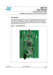
UM0919
User Manual
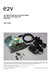
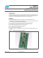
STM32VLDISCOVERY
STM32 value line Discovery
Introduction
The STM32 value line Discovery evaluation board helps you discover the STM32 value line
features and to develop and share your applications. It is based on an STM32F100RB and
includes ST-Link embedded debug tool interface, LEDs and push buttons.
Features
■
STM32F100RBT6B microcontroller, 128 KB Flash, 8 KB RAM in 64-pin LQFP
■
On-board ST-Link with selection mode switch to use the kit as a stand-alone ST-Link (with
SWD connector for programming and debugging)
■
Two red LEDs; LD1 for USB communication, LD2 for 3.3 volts power on
■
Designed to be powered by USB or an external supply of 5 V or 3.3 V
■
Can supply target application with 5 volts and 3 volts
■
Two user LEDs, LD3 and LD4 (green and blue)
■
Two push buttons (User and Reset)
■
Extension header for all QFP64 I/Os for quick connection to prototyping board or easy
probing
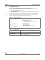
Figure 1.
September 2010
STM32 value line Discovery board
Doc ID 17217 Rev 1
1/22
www.st.com
Contents
UM0919
Contents
1
2
Quick start . . . . . . . . . . . . . . . . . . . . . . . . . . . . . . . . . . . . . . . . . . . . . . . . . 3
1.1
Getting started . . . . . . . . . . . . . . . . . . . . . . . . . . . . . . . . . . . . . . . . . . . . . . 3
1.2
System requirements . . . . . . . . . . . . . . . . . . . . . . . . . . . . . . . . . . . . . . . . . 3
1.3
Development toolchains . . . . . . . . . . . . . . . . . . . . . . . . . . . . . . . . . . . . . . . 3
1.4
Demonstration software . . . . . . . . . . . . . . . . . . . . . . . . . . . . . . . . . . . . . . . 3
1.5
Order code . . . . . . . . . . . . . . . . . . . . . . . . . . . . . . . . . . . . . . . . . . . . . . . . . 3
Hardware and layout . . . . . . . . . . . . . . . . . . . . . . . . . . . . . . . . . . . . . . . . . 4
2.1
STM32F100RBT6B microcontroller . . . . . . . . . . . . . . . . . . . . . . . . . . . . . . 7
2.2
Embedded ST-Link . . . . . . . . . . . . . . . . . . . . . . . . . . . . . . . . . . . . . . . . . . . 9
2.2.1
Using the ST-Link to program/debug the STM32 on board . . . . . . . . . . 10
2.2.2
Using the ST-Link to program/debug an external STM32 application . . 10
2.3
Power supply and power selection . . . . . . . . . . . . . . . . . . . . . . . . . . . . . . 11
2.4
LEDs . . . . . . . . . . . . . . . . . . . . . . . . . . . . . . . . . . . . . . . . . . . . . . . . . . . . 11
2.5
Push buttons . . . . . . . . . . . . . . . . . . . . . . . . . . . . . . . . . . . . . . . . . . . . . . 11
2.6
JP1 (Idd) . . . . . . . . . . . . . . . . . . . . . . . . . . . . . . . . . . . . . . . . . . . . . . . . . . 12
2.7
Solder bridges . . . . . . . . . . . . . . . . . . . . . . . . . . . . . . . . . . . . . . . . . . . . . 12
3
Extension connection . . . . . . . . . . . . . . . . . . . . . . . . . . . . . . . . . . . . . . . 13
4
Electrical schematics . . . . . . . . . . . . . . . . . . . . . . . . . . . . . . . . . . . . . . . 17
5
Revision history . . . . . . . . . . . . . . . . . . . . . . . . . . . . . . . . . . . . . . . . . . . 21
2/22
Doc ID 17217 Rev 1
UM0919
1
Quick start
Quick start
The STM32 value line Discovery is a low-cost and easy-to-use development kit to quickly
evaluate and start a development with an STM32 value line microcontroller.
Before installing and using the product, please accept the Evaluation Product License
Agreement from www.st.com/stm32-discovery.
For more information on the STM32 value line Discovery and for demonstration software
visit www.st.com/stm32-discovery.
1.1
Getting started
1.
Connect the STM32 value line Discovery board to a PC with a USB cable to power the
board.
2.
Press the USER button B1 (on bottom left corner of the board).
3.
Observe how the green LED LD3 blinking changes according to USER button B1
clicks.
4.
Each click on USER button B1 is confirmed by the blue LED LD4.
To study or modify the DISCOVER project related to this simple demo, visit
www.st.com/stm32-discovery and download the getting started documentation and free
software examples. This site also contains information on the STM32 features,
demonstration software and examples from which you can develop your own applications.
1.2
1.3
1.4
System requirements
●
Windows PC (2000, XP, Vista)
●
A/mini-B USB cable
Development toolchains
●
Atollic, TrueSTUDIO® (including the free LiteTrueSTUDIO®)
●
IAR, Embedded Workbench® for ARM
●
Keil, MDK-ARMTM
Demonstration software
Demonstration software is preloaded in the board's Flash memory for easy demonstration of
the device peripherals in stand-alone mode. For more information and to download the
latest version available, please refer to the STM32 value line Discovery demonstration
software available on www.st.com.
1.5
Order code
To order the STM32 value line Discovery, use the order code STM32VLDISCOVERY.
Doc ID 17217 Rev 1
3/22
Hardware and layout
2
UM0919
Hardware and layout
The STM32 value line Discovery is designed around the STM32F100RBT6B microcontroller
in a 64-pin LQFP package.
Figure 2 illustrates the connections between the STM32F100RB and its peripherals (STLink, push button, LED and connectors).
Figure 3 and Figure 4 help you to locate these features on the STM32 value line Discovery.
Figure 2.
Hardware block diagram
Mini
USB
Embedded ST-Link
SWD
I/O
I/O
I/O
Green LED
LD3
B2
RST
Blue LED
LD4
B1
USER
P3 Header
4/22
RESET
Doc ID 17217 Rev 1
P1 Header
P2 Header
STM32F100RB
UM0919
Hardware and layout
Figure 3.
Top layout
ST-Link USB connector
D1 diode
P2 connector
P1 connector
D2 diode
LD1 COM
LD2 power
SWD connector
ST-Link/Discovery
selector
R15
R14
SB1 VBAT
JP1 Idd
U3
STM32F100RB
SB2 BOOT1
B2 RST
B1 USER
LD4 PC8
LD3 PC9
P3 connector
Doc ID 17217 Rev 1
5/22
Hardware and layout
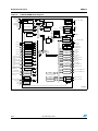
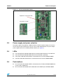
Figure 4.
UM0919
Bottom layout
Reserved
Do not modify
Reserved
Do not modify
SB12, SB13
SB14, SB15
SB11
RESET
SB16
BOOT0
SB17
SWDIO
SB18
SWCLK
6/22
Doc ID 17217 Rev 1
UM0919
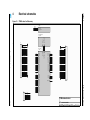
2.1
Hardware and layout
STM32F100RBT6B microcontroller
Figure 5.
STM32F100RB package
The STM32F100RB 32-bit microcontroller offers:
128 Kbytes of Flash memory
8 Kbytes RAM
LQFP64 10 x 10 mm
This device provides the following benefits:
●
Reduced system cost:
–
Built-in POR, PDR, LVD, watchdog timer.
–
Factory trimmed 8 MHz RC oscillator and 40 kHz for RTC and watchdog.
–
On-chip 12-bit dual channel DAC with DMA support and output buffers.
●
Perfect fit for control applications: Up to seven PWM 16-bit timers including advanced
control timer for a total of 26 channels.
●
Ideal for appliance control applications including induction cooking: Three independent
PWM 16-bit timers with complementary output and dead-time generation.
●
Reduced design complexity and minimized CPU, peripheral and memory use:
Consumer electronics control (CEC) peripheral.
●
Extensive connectivity capability: CEC, 400 kHz I²C, up to12 Mbit/s master and slave
SPI, up to 3 Mbit/s USART.
●
Achieves superior performance with 16-bit code density: ARM Cortex-M3 Thumb-2
32-bit instruction set and 7-channel DMA.
●
Eases Flash memory integrity check: CRC (cyclic redundancy check) with DMA
support.
For more information see the STM32F100xB datasheet (Doc ID 16455) on the ST website.
Doc ID 17217 Rev 1
7/22
Hardware and layout
STM32F100RB block diagram
AS!&
.*4234
*4$)
*4#+37#,+
*4-337$)/
*4$/
AS!&
40)*
37*4!'
%4TRACETRIGGER
4RACE
CONTROLLER
PBUS
)BUS
#ORTEX-#05
FMAX -(Z
.6)#
'0$-!
6OLTAGEREG
6TO6
&LASH+"
BIT
32!-
+"
6$$!
0/2
2ESET
3UPPLY SUPERVISION
)NT
0/20$2
2#(3
6$$!
CHANNELS
0!;=
'0)/PORT!
0";=
'0)/PORT"
0#;=
'0)/PORT#
0$;=
'0)/PORT$
0%;=
'0)/PORT%
!("& MAX -(Z
%84) 4
7+50
6$$
84!,/3#
-(Z
0,,
!&
633
.234
6$$!
633!
06$
2#,3
2ESET
CLOCK
CONTROL 6$$6TO6
6$$
$BUS
3YSTEM
0OWER
6$$
&LASH OBL
INTERFACE
42!#%#,+
42!#%$;=
"USMATRIX
Figure 6.
UM0919
/3#?).
/3#?/54
)7$'
0#,+
0#,+
(#,+
&#,+
3TANDBY
INTERFACE
6"! 46TO6
6"!4
84!, K(Z
24#
!75
"ACKUP
REGISTER
/3#?).
/3#?/54
4!- 0%224#
!,!2-/54
"ACKUPINTERFACE
!("
!0" CHANNELS
AS!&
CHANNELS
AS!&
4)-
!("
!0"
4)-
CHANNELCOMPL
CHANNELAND"+).
AS!&
4)-
CHANNELCOMPL
CHANNELAND"+).
AS!&
4)-
CHANNELSCOMPL
CHANNELS%42AND
"+).AS!&
4)-
-/3)-)3/
3#+.33AS!&
30)
2848#43243
#+AS!&
53!24
6
BIT!$# )&
4)-
53!24
53!24
30)
($-)#%#
CHANNELS
AS!&
2848#43243
#+AS!&
2848#43243
#+AS!&
-/3)-)3/
3#+.33AS!&
($-)#%#AS!&
3#,3$!3-"!AS!&
)#
77$'
4EMP SENSOR
!$#CHANNELS
!$#?).X
!0"& MAX -(Z
4)-
!0" & MAX -(Z
CHANNELSCOMPL
CHANNELAND"+).
AS!&
)#
3#,3$!3-"!AS!&
4)-
)& BIT$!#
)&
$!#?/54AS!&
4)-
BIT$!#
$!# ?/54AS!&
2%&
6
2%&n
6$$!
6$$!
AIB
8/22
Doc ID 17217 Rev 1
UM0919
2.2
Hardware and layout
Embedded ST-Link
The ST-Link programming and debugging tool is integrated on the STM32 value line
Discovery. The embedded ST-Link can be used in 2 different ways:
●
to program/debug the MCU on board
●
to program/debug an MCU in another application board using a cable connected to
SWD connector CN2.
For information about debugging and programming features refer to ST-Link UM0627.
Note:
UM0627 contains information about all the ST-Link features. Usage in this situation is
restricted to STM32F devices and SWD support only (no JTAG).
Figure 7.
Typical configuration
Hardware requirements:
- USB cable type A to mini-B
- Computer with Windows 2000, XP or Vista OS
Development toolchain:
- Atollic, TrueSTUDIO®
- IAR, Embedded Workbench® for ARM
- Keil, MDK-ARMTM
Table 1.
Jumper states
Jumper state
Description
CN3 jumpers ON
ST-Link functions enabled for on board programming (default)
CN3 jumpers OFF
ST-Link functions enabled for external application through CN2
connector (SWD supported).
Doc ID 17217 Rev 1
9/22
Hardware and layout
2.2.1
UM0919
Using the ST-Link to program/debug the STM32 on board
To program the STM32 on board, simply plug in the two jumpers on CN3, but do not use the
CN2 connector as that could disturb communication with the STM32F100RB of the STM32
value line Discovery.
Figure 8.
Discovery connections image
Jumpers on CN3
2.2.2
Using the ST-Link to program/debug an external STM32 application
It is very easy to use the ST-Link to program the STM32 on an external application. You
simply remove the 2 jumpers from CN3 and connect your application to the CN2 debug
connector (as shown in Figure 9 and according to Table 2.).
Note:
Only SWD is supported, not JTAG.
Table 2.
Debug connector CN2 (SWD)
Pin
10/22
CN2
Designation
1
VDD_TARGET
VDD from application
2
SWCLK
SWD clock
3
GND
Ground
4
SWDIO
SWD data input/output
Doc ID 17217 Rev 1
UM0919
Hardware and layout
Figure 9.
ST-Link connections image
Application connected to CN2
No jumpers on CN3
2.3
Power supply and power selection
The power supply is provided by a USB connector or external power supply (5 V or 3.3V ).
The 5V (P2 pin 26) and 3V3 (P1 pin 3) pins can be used independently as input or output
power supplies due to D1 and D2 protection diodes (see Figure 3).
2.4
2.5
LEDs
●
LD1: Red LED LD1 labeled COM indicates communication between PC and ST-Link.
●
LD2: Red LED LD2 labeled PWR indicates that the board is powered.
●
LD3: Green LED LD3 labeled PC9 is connected to the I/O PC9 of STM32F100RB.
●
LD4: Blue LED LD4 labeled PC8 is connected to the I/O PC8 of STM32F100RB.
Push buttons
●
B1: Push button B1 labeled USER is connected to the I/O PA0 of STM32F100RB and
can be used as WAKE-UP.
●
B2: Push button B2 labeled RST is dedicated to the RESET pin of STM32F100RB.
Doc ID 17217 Rev 1
11/22
Hardware and layout
2.6
UM0919
JP1 (Idd)
Jumper JP1, labeled Idd, allows the consumption of STM32F100RB to be measured by
removing the jumper and connecting an ammeter.
●
Jumper on: STM32F100RB is powered (default).
●
Jumper off: STM32F100RB is not powered.
2.7
Solder bridges
Table 3.
Solder bridge description
Bridge
State(1)
Description
Off
VDD_MCU is not connected to VBAT of STM32F100RB. VBAT could be
connected to an external power supply through EXT_VBAT.
On
VBAT of STM32F100RB is connected to VDD_MCU.
Off
BOOT1 (PB2) signal is connected to +3.3V through pull-up resistor.
On
BOOT1 (PB2) signal is connected to GND through pull-down resistor.
SB3,5,7,9 (DEFAULT)
On
Reserved. Do not modify.
SB4,6,8,10 (PRG-32)
Off
Reserved. Do not modify.
Off
RESET of STM32F100RB is disconnected from T_JRST of ST-Link.
On
RESET of STM32F100RB is connected to T_JRST of ST-Link.
Off
PD1 is not connected to external pin and the X2 can be used. (2)
On
PD1 is connected to external pin and can be used as GPIO, X2 is not available.
Remove (unsolder) R14.
Off
PD0 is not connected to external pin and the X2 can be used.(2)
On
PD0 is connected to external pin and can be used as GPIO, X2 is not available.
Remove (unsolder) R14.
Off
PC15 is not connected to external pin and the X3 can be used.(2)
On
PC15 is connected to external pin and can be used as GPIO, X3 is not available.
Remove (unsolder) R15.
Off
PC14 is not connected to external pin and the X3 can be used.(2)
On
PC14 is connected to external pin and can be used as GPIO, X3 is not available.
Remove (unsolder) R15.
Off
BOOT0 signal is connected to +3.3 V through pull-up resistor.
On
BOOT0 signal is connected to GND through pull-down resistor.
Off
SWDIO and PA13 of STM32F100RB are not connected, SWD not available.
On
SWDIO and PA13 of STM32F100RB are connected, SWD available.
Off
SWCLK and PA14 of STM32F100RB are not connected, SWD not available
On
SWCLK and PA14 of STM32F100RB are connected, SWD available.
SB1 (VBAT)
SB2 (BOOT1)
SB11 (RESET)
SB12 (X2)
SB13 (X2)
SB14 (X3)
SB15 (X3)
SB16 (BOOT0)
SB17 (SWDIO)
SB18 (SWCLK)
1. Factory state is in bold type.
2. If the resistor has been removed to modify the default setting of this bridge, it must be resoldered.
12/22
Doc ID 17217 Rev 1
UM0919
Extension connection
Male headers P1, P2 and P3 can connect the STM32 value line Discovery to a standard
prototyping/wrapping board. All GPIOs of STM32F100RB are available on it.
P1, P2 and P3 can also be used to probe an oscilloscope, logical analyzer or voltmeter.
Table 4.
P1 pinout
Pin number Pin number
(P1)
(chip)
Type
3
Extension connection
Board pin
name
Main function
1
12/31/47/63 GND
-
Vss
2
-
NC
-
-
3V3
-
-
S
VBAT
3
4
1
VBAT
5
2
PC13
I/O Port C13
TAMPER-RTC
(1)
I/O Port C14
OSC32_IN
I/O Port C15
OSC32_OUT
6
3
PC14
7
4
PC15(1)
8
5
Alternate
function
(1)
I/O OSC_IN
(1)
PD0
9
6
PD1
I/O OSC_OUT
10
7
NRST
I/O RESET
11
8
PC0
I/O Port C0
ADC1_IN10
12
9
PC1
I/O Port C1
ADC1_IN11
13
10
PC2
I/O Port C2
ADC1_IN12
14
11
PC3
I/O Port C3
ADC1_IN13
15
14
PA0
I/O Port A0
WKUP /
USART2_CTS/
ADC1_IN0 /
TIM2_CH1_ETR
16
15
PA1
I/O Port A1
USART2_RTS/
ADC1_IN1 /
TIM2_CH2
I/O Port A2
USART2_TX/
ADC1_IN2 /
TIM2_CH3/
TIM15_CH1
I/O Port A3
USART2_RX/
ADC1_IN3 /
TIM2_CH4 /
TIM15_CH2
I/O Port A4
SPI1_NSS/
ADC1_IN4
USART2_CK /
DAC1_OUT
17
18
19
16
17
20
PA2
PA3
PA4
Doc ID 17217 Rev 1
Remap
13/22
Extension connection
P1 pinout (continued)
Pin number Pin number
(P1)
(chip)
Board pin
name
Type
Table 4.
UM0919
Main function
Alternate
function
Remap
20
21
PA5
I/O Port A5
SPI1_SCK/
ADC1_IN5 /
DAC2_OUT
21
22
PA6
I/O Port A6
SPI1_MISO/
ADC1_IN6 /
TIM3_CH1
TIM1_BKIN /
TIM16_CH1
22
23
PA7
I/O Port A7
SPI1_MOSI/
ADC1_IN7 /
TIM3_CH2
TIM1_CH1N /
TIM17_CH1
23
24
PC4
I/O Port C4
ADC1_IN14
24
25
PC5
I/O Port C5
ADC1_IN15
25
26
PB0
I/O Port B0
ADC1_IN8/
TIM3_CH3
TIM1_CH2N
26
27
PB1
I/O Port B1
ADC1_IN9/
TIM3_CH4
TIM1_CH3N
27
28
PB2
I/O
28
Port B2/
BOOT1
GND
1. Alternate pin, connected by default to STM32F100RB oscillator.
P2 pinout
Pin number Pin number
(P2)
(chip)
14/22
Pin name
Type
Table 5.
Main function
Alternate
function
1
29
PB10
I/O Port B10
I2C2_SCL/
USART3_TX
TIM2_CH3/
CEC
2
30
PB11
I/O Port B11
I2C2_SDA/
USART3_RX
Remap
TIM2_CH4
3
33
PB12
I/O Port B12
SPI2_NSS/
I2C2_SMBA/
TIM1_BKIN/
USART3_CK
4
34
PB13
I/O Port B13
SPI2_SCK /
TIM1_CH1N
USART3_CTS
5
35
PB14
I/O Port B14
SPI2_MISO/
TIM1_CH2N /
USART3_RTS
TIM15_CH1
6
36
PB15
I/O Port B15
SPI2_MOSI /
TIM1_CH3N /
TIM15_CH1N
TIM15_CH2
Doc ID 17217 Rev 1
UM0919
Extension connection
P3 pinout
Pin number Pin number
(P3)
(chip)
Pin name
1
GND
2
NC
Type
Table 6.
Main function
Alternate
function
Remap
3
38
PC7
I/O Port C7
TIM3_CH2
4
39
PC8
I/O Port C8
TIM3_CH3
5
40
PC9
I/O Port C9
TIM3_CH4
6
41
PA8
I/O Port A8
USART1_CK /
MCO
TIM1_CH1
7
42
PA9
I/O Port A9
USART1_TX /
TIM1_CH2
TIM15_BKIN
8
43
PA10
I/O Port A10
USART1_RX /
TIM1_CH3
TIM17_BKIN
9
44
PA11
I/O Port A11
USART1_CTS /
TIM1_CH4
10
45
PA12
I/O Port A12
USART1_RTS /
TIM1_ETR
11
46
PA13
I/O
12
49
PA14
I/O JTCK/ SWCLK
PA14
JTMS/
SWDIO
PA13
13
50
PA15
I/O JTDI
TIM2_CH1_ETR
/ PA15/
SPI1_NSS
14
51
PC10
I/O Port C10
USART3_TX
15
52
PC11
I/O Port C11
USART3_RX
16
53
PC12
I/O Port C12
USART3_CX
17
54
PD2
I/O Port D2
18
55
PB3
I/O JTDO
TIM2_CH2 / PB3
TRACESWO
SPI1_SCK
19
56
PB4
I/O NJTRST
PB4 / TIM3_CH1
SPI1_MISO
20
57
PB5
I/O Port B5
I2C1_SMBA /
TIM16_BKIN
TIM3_CH2 /
SPI1_MOSI
21
58
PB6
I/O Port B6
I2C1_SCL/
TIM4_CH1
TIM16_CH1N
USART1_TX
22
59
PB7
I/O Port B7
I2C1_SDA/
TIM17_CH1N
TIM4_CH2
USART1_RX
Doc ID 17217 Rev 1
TIM3_ETR
15/22
Extension connection
P3 pinout (continued)
Pin number Pin number
(P3)
(chip)
16/22
Type
Table 6.
UM0919
Pin name
Main function
Alternate
function
Remap
23
60
BOOT0
I
24
61
PB8
I/O Port B8
TIM4_CH3 /
TIM16_CH1 /
CEC
I2C1_SCL
25
62
PB9
I/O Port B9
TIM4_CH4 /
TIM17_CH1
I2C1_SDA
26
EXT_5V
27
NC
28
GND
BOOT0
Doc ID 17217 Rev 1
Electrical schematics
UM0919
4
Figure 10. STM32 value line Discovery
Power.SchDoc
U_Power
EXT_5V
EXT_3V3
EXT_VBAT
EXT_5V
EXT_3V3
EXT_VBAT
P1
Header 28
1
2
3
4
5
6
Header 6
PB10
PB11
PB12
PB13
PB14
PB15
PB15
PB14
PB13
PB12
PB11
PB10
PB9
PB8
PB7
PB6
PB5
PB4
PB3
PB2
PB1
PB0
PA15
PA14
PA13
PA12
PA11
PA10
PA9
PA8
PA7
PA6
PA5
PA4
PA3
PA2
PA1
PA0
PB15
PB14
PB13
PB12
PB11
PB10
PB9
PB8
PB7
PB6
PB5
PB4
PB3
PB2
PB1
PB0
RESET#
PA15
PA14
PA13
PA12
PA11
PA10
PA9
PA8
PA7
PA6
PA5
PA4
PA3
PA2
PA1
PA0
PC15
PC14
PC13
PC12
PC11
PC10
PC9
PC8
PC7
PC6
PC5
PC4
PC3
PC2
PC1
PC0
PD2
PD1
PD0
BOOT0
PC15
PC14
PC13
PC12
PC11
PC10
PC9
PC8
PC7
PC6
PC5
PC4
PC3
PC2
PC1
PC0
PD2
PD1
PD0
EXT_5V
PB9
PB8
BOOT0
PB7
PB6
PB5
PB4
PB3
PD2
PC12
PC11
PC10
PA15
PA14
PA13
PA12
PA11
PA10
PA9
PA8
PC9
PC8
PC7
PC6
BOOT0
28
27
26
25
24
23
22
21
20
19
18
17
16
15
14
13
12
11
10
9
8
7
6
5
4
3
2
1
Header 28
STMicroelectronics
17/22
Title:
STM32-DISCOVERY
Number:MB913
Rev: C.2(PCB.SCH)
Date: 7/15/2010
Sheet 1
of
4
Electrical schematics
P3
MCU.SchDoc
U_MCU
RESET#
P2
EXT_3V3
EXT_VBAT
PC13
PC14
PC15
PD0
PD1
R23
RESET#
PC0 820
PC1
PC2
PC3
PA0
PA1
PA2
PA3
PA4
PA5
PA6
PA7
PC4
PC5
PB0
PB1
PB2
TCK/SWCLK
TMS/SWDIO
Doc ID 17217 Rev 1
1
2
3
4
5
6
7
8
9
10
11
12
13
14
15
16
17
18
19
20
21
22
23
24
25
26
27
28
TCK/SWCLK
TMS/SWDIO
RESET#
ST_LINK.SCHDOC
U_ST_LINK
1
2
3
Electrical schematics
18/22
Figure 11. STM32 value line MCU
4
X3
MC306-G-06Q-32.768 (manufacturer JFVNY)
BOOT1
+3V3
C11
6.8pF
R19
10K
PB2
R15
0
U3A
R18
510
SB2
TMS/SWDIO
TCK/SWCLK
SB17
SB18
PA0
PA1
PA2
PA3
PA4
PA5
PA6
PA7
PA8
PA9
PA10
PA11
PA12
PA15
Doc ID 17217 Rev 1
PA13
PA14
PA13
PA14
PB0
PB1
PB2
PB3
PB4
PB5
PB6
PB7
PB8
PB9
PB10
PB11
PB12
PB13
PB14
PB15
PA0
PA1
PA2
PA3
PA4
PA5
PA6
PA7
PA8
PA9
PA10
PA11
PA12
PA13
PA14
PA15
14
15
16
17
20
21
22
23
41
42
43
44
45
46
49
50
PB0
PB1
PB2
PB3
PB4
PB5
PB6
PB7
PB8
PB9
PB10
PB11
PB12
PB13
PB14
PB15
26
27
28
55
56
57
58
59
61
62
29
30
33
34
35
36
USER & WAKE-UP Button
PA0 PC15-OSC32_OUT
PA1
PC14-OSC32_IN
PA2
PC13
PA3
PC12
PA4
PC11
PA5
PC10
PA6
PC9
PA7
PC8
PA8
PC7
PA9
PC6
PA10
PC5
PA11
PC4
PA12
PC3
PA13
PC2
PA14
PC1
PA15
PC0
4
3
2
53
52
51
40
39
38
37
25
24
11
10
9
8
PC13
PC12
PC11
PC10
PC9
PC8
PC7
PC6
PC5
PC4
PC3
PC2
PC1
PC0
54
PD2
3
2
4
1
C17
6.8pF
Must be close to the Crystal and open
SB14
SB15
PC15
PC14
PC9
LD3
R25
330
PC8
green
LD4
R26
660
blue
X2
ESA8.00000F20D25F(with socket)
PB0
PB1
PB2
PB3
PB4
PB5
PB6
PB7
PB8
PB9
PB10
PB11
PB12
PB13
PB14
PB15
PD2
OSC_IN
OSC_OUT
NRST
BOOT0
5
6
PD2
C13
20pF
OSC_IN
OSC_OUT
C12
R14
220
RESET#
7
SB12
SB13
R16
510
BOOT0
60
20pF
PD1
PD0
SB16
STM32F100RBT6B
R17
10K
BOOT0
Must be close to the Crystal and open
+3V3
R20
BOOT0
100
RESET Button
4
1
R22
+3V3
B2
SW-PUSH-CMS
SW-PUSH-CMS
B1
3
2
C22
[N/A]
PA0
PC15
PC14
PC13
PC12
PC11
PC10
PC9
PC8
PC7
PC6
PC5
PC4
PC3
PC2
PC1
PC0
1
4
2
3
RESET#
RESET#
0
R21
10K
C23
100nF
+3V3
R24
STMicroelectronics
[N/A]
STM32-DISCOVERY STM32 Value Line
Number:MB913
1
2
3
Rev: C.2(PCB.SCH)
Date: 7/15/2010
4
Sheet 2
of
4
UM0919
Title:
UM0919
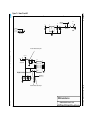
Figure 12. Power 5V and 3V3
TP1
+5V
D2
C1
10uF
+5V
Vout
R5
2
C2
10uF
1
BAT60JFILM
2
1K
C3
100nF
BAT60JFILM
PWR
1
U5V_ST_LINK
Vin
LD2
red
+3V3
D1
GND
3
EXT_5V
EXT_3V3
U1
LD1117DT33C
Lx and Cx Must be close to the pin 13
Doc ID 17217 Rev 1
VDD_MCU
JP1
L1
+3V3
Closed by default
fcm1608-0603 C14
1uF
U3B
C15
100nF
13
32
48
64
19
SB1
1
VDD_MCU is Dédicated Power Plan
VDDA
VDD_1
VDD_2
VDD_3
VDD_4
VSSA
VSS_1
VSS_2
VSS_3
VSS_4
12
31
47
63
18
SWIM
VBAT
STM32F100RBT6B
EXT_VBAT
C21
100nF
C20
100nF
C18
100nF
C19
100nF
C16
1uF
LED
STMicroelectronics
19/22
Title:
STM32-DISCOVERY Power 5V & 3V3
Number:MB913
Rev: C.2(PCB.SCH)
Date: 7/15/2010
Sheet 3
of
4
Electrical schematics
SBx and Cx Must be close to the pin 1
1
2
3
4
SWD
R7
T_JRST
TCK/SWCLK
TMS/SWDIO
RESET#
SB11
ESA8.00000F20D25F
JTAG_CTL
100K
C10
100nF+3V3
VBAT
PC13
PC14
PC15
OSC_IN
OSC_OUT
/RST
VSSA
VDDA
PA0
PA1
U2_TX
36
35
34
33
32
31
30
29
28
27
26
25
R11
22
R12
PRG-32
SB3
22
+3V3
SB4
SB5
SB6
SB7
SB8
SB9
SB10
STM_JTCK
SWCLK
STM_JTMS
SWDIO
T_JTMS
STM_JTMS
USB_DP
USB_DM
D3
D4
LED_STLINK
T_JTMS
T_JTCK
CN3
Jumpers ON --> DISCOVERY Selected
Jumpers OFF --> ST-LINK Selected
13
14
15
16
17
18
19
20
21
22
23
24
AIN_1
+3V3
VDD_2
VSS_2
JTMS
PA12
PA11
PA10
PA9
PA8
S2_MOSI
S2_MISO
S2_CK
PB12
+3V3
R9
R10
4K7
4K7
T_JTCK
T_JTDO
T_JTDI
T_NRST
T_JRST
Doc ID 17217 Rev 1
R13
+3V3
1
2
3
4
5
6
7
8
9
10
11
12
T_JTCK
1
2
3
4
SWD
1
2
3
4
+3V3
CN2
Z5V1
2
C8
20pF
VDD_3
VSS_3
PB9
PB8
BOOT0
PB7
PB6
PB5
JNRST
JTDO
JTDI
JTCK
1
X1
U2_RX
U2_CK
S1_CK
S1_MISO
S1_MOSI
PB0
PB1
PB2/BOOT1
PB10
PB11
VSS_1
VDD_1
C9
20pF
R8
10K
U2
STM32F103C8T6
Z5V1
48
47
46
45
44
43
42
41
40
39
38
37
+3V3
DEFAULT
STM_JRST
STM_JTDO
STM_JTDI
STM_JTCK
100K
Electrical schematics
20/22
Figure 13. ST-Link (SWD only)
SWIM
+3V3
+3V3
U5V_ST_LINK
R2
1K5
CN1
VCC
DD+
ID
GND
SHELL
+3V3
1
2
3
4
5
0
R4
R3
22
USB_DM
USB_DP
COM
LED_STLINK
22
LD1
R6
510
red
R1
100K
5075BMR-05-SM
C6
100nF
C7
100nF
C5
100nF
C4
100nF
USB
LED
STMicroelectronics
MCU
STM32-DISCOVERY ST_LINK (SWD only)
Number:MB913
1
2
3
Rev: C.2(PCB.SCH)
Date: 7/15/2010
4
Sheet 4
of
4
UM0919
Title:
UM0919
5
Revision history
Revision history
Table 7.
Date
10-Sep-2010
Document revision history
Revision
1
Changes
Initial release.
Doc ID 17217 Rev 1
21/22
UM0919
Please Read Carefully:
Information in this document is provided solely in connection with ST products. STMicroelectronics NV and its subsidiaries (“ST”) reserve the
right to make changes, corrections, modifications or improvements, to this document, and the products and services described herein at any
time, without notice.
All ST products are sold pursuant to ST’s terms and conditions of sale.
Purchasers are solely responsible for the choice, selection and use of the ST products and services described herein, and ST assumes no
liability whatsoever relating to the choice, selection or use of the ST products and services described herein.
No license, express or implied, by estoppel or otherwise, to any intellectual property rights is granted under this document. If any part of this
document refers to any third party products or services it shall not be deemed a license grant by ST for the use of such third party products
or services, or any intellectual property contained therein or considered as a warranty covering the use in any manner whatsoever of such
third party products or services or any intellectual property contained therein.
UNLESS OTHERWISE SET FORTH IN ST’S TERMS AND CONDITIONS OF SALE ST DISCLAIMS ANY EXPRESS OR IMPLIED
WARRANTY WITH RESPECT TO THE USE AND/OR SALE OF ST PRODUCTS INCLUDING WITHOUT LIMITATION IMPLIED
WARRANTIES OF MERCHANTABILITY, FITNESS FOR A PARTICULAR PURPOSE (AND THEIR EQUIVALENTS UNDER THE LAWS
OF ANY JURISDICTION), OR INFRINGEMENT OF ANY PATENT, COPYRIGHT OR OTHER INTELLECTUAL PROPERTY RIGHT.
UNLESS EXPRESSLY APPROVED IN WRITING BY AN AUTHORIZED ST REPRESENTATIVE, ST PRODUCTS ARE NOT
RECOMMENDED, AUTHORIZED OR WARRANTED FOR USE IN MILITARY, AIR CRAFT, SPACE, LIFE SAVING, OR LIFE SUSTAINING
APPLICATIONS, NOR IN PRODUCTS OR SYSTEMS WHERE FAILURE OR MALFUNCTION MAY RESULT IN PERSONAL INJURY,
DEATH, OR SEVERE PROPERTY OR ENVIRONMENTAL DAMAGE. ST PRODUCTS WHICH ARE NOT SPECIFIED AS "AUTOMOTIVE
GRADE" MAY ONLY BE USED IN AUTOMOTIVE APPLICATIONS AT USER’S OWN RISK.
Resale of ST products with provisions different from the statements and/or technical features set forth in this document shall immediately void
any warranty granted by ST for the ST product or service described herein and shall not create or extend in any manner whatsoever, any
liability of ST.
ST and the ST logo are trademarks or registered trademarks of ST in various countries.
Information in this document supersedes and replaces all information previously supplied.
The ST logo is a registered trademark of STMicroelectronics. All other names are the property of their respective owners.
© 2010 STMicroelectronics - All rights reserved
STMicroelectronics group of companies
Australia - Belgium - Brazil - Canada - China - Czech Republic - Finland - France - Germany - Hong Kong - India - Israel - Italy - Japan Malaysia - Malta - Morocco - Philippines - Singapore - Spain - Sweden - Switzerland - United Kingdom - United States of America
www.st.com
22/22
Doc ID 17217 Rev 1