1
UM1570
User manual
STM32F3DISCOVERY
Discovery kit for STM32F303xx microcontrollers
Introduction
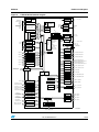
The STM32F3DISCOVERY is designed to help you explore the features of the STM32 F3
32-bit ARM® Cortex™-M4 mixed-signal MCU, and develop your applications. It is based on
an STM32F303VCT6 and includes an ST-LINK/V2 embedded debug tool interface,
Gyroscope ST MEMS, E-compass with accelerometer ST MEMS, LEDs, pushbuttons and a
USB mini-B connector.
Figure 1.
STM32F3DISCOVERY
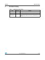
Table 1.
Applicable tools
February 2013
Type
Part number
Evaluation tools
STM32F3DISCOVERY
Doc ID 023594 Rev 3
1/36
www.st.com
Contents
UM1570
Contents
1
Conventions . . . . . . . . . . . . . . . . . . . . . . . . . . . . . . . . . . . . . . . . . . . . . . . . 5
2
Quick start . . . . . . . . . . . . . . . . . . . . . . . . . . . . . . . . . . . . . . . . . . . . . . . . . 6
2.1
Getting started . . . . . . . . . . . . . . . . . . . . . . . . . . . . . . . . . . . . . . . . . . . . . . 6
2.2
System requirements . . . . . . . . . . . . . . . . . . . . . . . . . . . . . . . . . . . . . . . . . 6
2.3
Development toolchain supporting the STM32F3DISCOVERY . . . . . . . . . 6
2.4
Order code . . . . . . . . . . . . . . . . . . . . . . . . . . . . . . . . . . . . . . . . . . . . . . . . . 6
3
Features . . . . . . . . . . . . . . . . . . . . . . . . . . . . . . . . . . . . . . . . . . . . . . . . . . . 7
4
Hardware and layout . . . . . . . . . . . . . . . . . . . . . . . . . . . . . . . . . . . . . . . . . 8
4.1
STM32F303VCT6 microcontroller . . . . . . . . . . . . . . . . . . . . . . . . . . . . . . 11
4.2
Embedded ST-LINK/V2 . . . . . . . . . . . . . . . . . . . . . . . . . . . . . . . . . . . . . . 14
4.2.1
Using ST-LINK/V2 to program/debug the STM32F303VCT6 on board . 14
4.2.2
Using ST-LINK/V2 to program/debug an external STM32 application . . 15
4.3
Power supply and power selection . . . . . . . . . . . . . . . . . . . . . . . . . . . . . . 17
4.4
LEDs . . . . . . . . . . . . . . . . . . . . . . . . . . . . . . . . . . . . . . . . . . . . . . . . . . . . 17
4.5
Pushbuttons . . . . . . . . . . . . . . . . . . . . . . . . . . . . . . . . . . . . . . . . . . . . . . . 17
4.6
USB device supported . . . . . . . . . . . . . . . . . . . . . . . . . . . . . . . . . . . . . . . 18
4.7
E-compass/accelerometer MEMS (ST MEMS LSM303DLHC) . . . . . . . . 18
4.8
Gyroscope MEMS (ST MEMS L3GD20) . . . . . . . . . . . . . . . . . . . . . . . . . 18
4.9
JP3 (Idd) . . . . . . . . . . . . . . . . . . . . . . . . . . . . . . . . . . . . . . . . . . . . . . . . . . 18
4.10
OSC clock . . . . . . . . . . . . . . . . . . . . . . . . . . . . . . . . . . . . . . . . . . . . . . . . 19
4.10.1
OSC clock supply . . . . . . . . . . . . . . . . . . . . . . . . . . . . . . . . . . . . . . . . . 19
4.10.2
OSC 32 kHz clock supply . . . . . . . . . . . . . . . . . . . . . . . . . . . . . . . . . . . 19
4.11
Solder bridges . . . . . . . . . . . . . . . . . . . . . . . . . . . . . . . . . . . . . . . . . . . . . 20
4.12
Extension connectors . . . . . . . . . . . . . . . . . . . . . . . . . . . . . . . . . . . . . . . . 21
5
Mechanical drawing . . . . . . . . . . . . . . . . . . . . . . . . . . . . . . . . . . . . . . . . 30
6
STM32F3DISCOVERY electrical schematics . . . . . . . . . . . . . . . . . . . . . 31
7
Revision history . . . . . . . . . . . . . . . . . . . . . . . . . . . . . . . . . . . . . . . . . . . 35
2/36
Doc ID 023594 Rev 3
UM1570
List of figures
List of figures
Figure 1.
Figure 2.
Figure 3.
Figure 4.
Figure 5.
Figure 6.
Figure 7.
Figure 8.
Figure 9.
Figure 10.
Figure 11.
Figure 12.
Figure 13.
Figure 14.
STM32F3DISCOVERY . . . . . . . . . . . . . . . . . . . . . . . . . . . . . . . . . . . . . . . . . . . . . . . . . . . . . 1
Hardware block diagram . . . . . . . . . . . . . . . . . . . . . . . . . . . . . . . . . . . . . . . . . . . . . . . . . . . . 8
Board layout (top view) . . . . . . . . . . . . . . . . . . . . . . . . . . . . . . . . . . . . . . . . . . . . . . . . . . . . . 9
Board layout (bottom view) . . . . . . . . . . . . . . . . . . . . . . . . . . . . . . . . . . . . . . . . . . . . . . . . . 10
STM32F303VCT6 package . . . . . . . . . . . . . . . . . . . . . . . . . . . . . . . . . . . . . . . . . . . . . . . . 11
STM32F303VCT6 block diagram . . . . . . . . . . . . . . . . . . . . . . . . . . . . . . . . . . . . . . . . . . . . 13
Typical configuration . . . . . . . . . . . . . . . . . . . . . . . . . . . . . . . . . . . . . . . . . . . . . . . . . . . . . . 14
STM32F3DISCOVERY connections image . . . . . . . . . . . . . . . . . . . . . . . . . . . . . . . . . . . . 15
ST-LINK/V2 connections image . . . . . . . . . . . . . . . . . . . . . . . . . . . . . . . . . . . . . . . . . . . . . 16
STM32F3DISCOVERY mechanical drawing . . . . . . . . . . . . . . . . . . . . . . . . . . . . . . . . . . . 30
STM32F3DISCOVERY top level . . . . . . . . . . . . . . . . . . . . . . . . . . . . . . . . . . . . . . . . . . . . 31
ST-LINK/V2 (SWD only) . . . . . . . . . . . . . . . . . . . . . . . . . . . . . . . . . . . . . . . . . . . . . . . . . . . 32
STM32F303VCT6 MCU . . . . . . . . . . . . . . . . . . . . . . . . . . . . . . . . . . . . . . . . . . . . . . . . . . . 33
Peripherals . . . . . . . . . . . . . . . . . . . . . . . . . . . . . . . . . . . . . . . . . . . . . . . . . . . . . . . . . . . . . 34
Doc ID 023594 Rev 3
3/36
List of tables
UM1570
List of tables
Table 1.
Table 2.
Table 3.
Table 4.
Table 5.
Table 6.
Table 7.
4/36
Applicable tools. . . . . . . . . . . . . . . . . . . . . . . . . . . . . . . . . . . . . . . . . . . . . . . . . . . . . . . . . . . 1
ON/OFF conventions . . . . . . . . . . . . . . . . . . . . . . . . . . . . . . . . . . . . . . . . . . . . . . . . . . . . . . 5
Jumper states . . . . . . . . . . . . . . . . . . . . . . . . . . . . . . . . . . . . . . . . . . . . . . . . . . . . . . . . . . . 14
Debug connector CN3 (SWD) . . . . . . . . . . . . . . . . . . . . . . . . . . . . . . . . . . . . . . . . . . . . . . 15
Solder bridges. . . . . . . . . . . . . . . . . . . . . . . . . . . . . . . . . . . . . . . . . . . . . . . . . . . . . . . . . . . 20
STM32F303VCT6 MCU pin description versus board function . . . . . . . . . . . . . . . . . . . . . 21
Document revision history . . . . . . . . . . . . . . . . . . . . . . . . . . . . . . . . . . . . . . . . . . . . . . . . . 35
Doc ID 023594 Rev 3
UM1570
1
Conventions
Conventions
Table 2 provides the definition of some conventions used in the present document.
Table 2.
ON/OFF conventions
Convention
Definition
Jumper JP1 ON
Jumper fitted
Jumper JP1 OFF
Jumper not fitted
Solder bridge SBx ON
SBx connections closed by solder
Solder bridge SBx OFF SBx connections left open
Doc ID 023594 Rev 3
5/36
Quick start
2
UM1570
Quick start
The STM32F3DISCOVERY is a low-cost and easy-to-use development kit to quickly
evaluate and start development with an STM32 F3 series microcontroller. Before installing
and using the product, please accept the Evaluation Product License Agreement from
www.st.com/stm32f3discovery. For more information on the STM32F3DISCOVERY and for
demonstration software, visit www.st.com/stm32f3discovery.
2.1
Getting started
Follow the sequence below to configure the STM32F3DISCOVERY board and launch the
DISCOVER application:
1.
Check the jumper positions on the board, JP3 on, CN4 on (DISCOVERY selected).
2.
Connect the STM32F3DISCOVERY board to a PC with a USB cable type A to mini-B
through the USB ST-LINK or USB USER connector to power the board. The red LEDs
LD1 (PWR) and LD2 (COM) light up.
3.
The eight LED indicators blink sequentially.
4.
Press the USER button to enable the MEMS gyroscope sensor.
5.
Observe how the blinking of the LEDs indicates the gyroscope movements.
6.
Press the USER button again to enable the MEMS e-compass sensor.
7.
Keep the board in a horizontal position. One of the eight LEDs lights up to indicate the
direction of the north.
8.
Tilt the board and the eight LEDs blink again
9.
To examine or modify the Discover project related to this demo, visit
www.st.com/stm32f3discovery and follow the tutorial. Discover the STM32F303xx MCU
features, download and execute programs proposed in the list of projects.
10. Develop your own application using the available examples.
2.2
2.3
2.4
System requirements
●
Windows PC (XP, Vista, 7)
●
USB type A to Mini-B USB cable
Development toolchain supporting the STM32F3DISCOVERY
●
Altium®, TASKING™ VX-toolset
●
ARM®, Atollic TrueSTUDIO®
●
IAR™, EWARM (IAR Embedded Workbench®)
●
Keil™, MDK-ARM™
Order code
To order the STM32F303xx Discovery kit, use the order code STM32F3DISCOVERY.
6/36
Doc ID 023594 Rev 3
UM1570
3
Features
Features
The STM32F3DISCOVERY offers the following features.
●
STM32F303VCT6 microcontroller featuring 256 KB of Flash memory, 48 KB of RAM in
an LQFP100 package.
●
On-board ST-LINK/V2 with selection mode switch to use the kit as a standalone
ST-LINK/V2 (with SWD connector for programming and debugging).
●
Board power supply: through the USB bus or from an external 3 V or 5 V supply
voltage.
●
External application power supply: 3 V and 5 V.
●
L3GD20, ST MEMS motion sensor, 3-axis digital output gyroscope.
●
LSM303DLHC, ST MEMS system-in-package featuring a 3D digital linear acceleration
sensor and a 3D digital magnetic sensor.
●
Ten LEDs:
–
LD1 (red) for 3.3 V power-on.
–
LD2 (red/green) for USB communication.
–
Eight user LEDs, LD3/10 (red), LD4/9 (blue), LD5/8 (orange) and LD6/7 (green).
●
Two pushbuttons (user and reset).
●
USB USER with Mini-B connector.
●
Extension header for LQFP100 I/Os for quick connection to prototyping board and easy
probing.
A large number of free ready-to-run application firmware examples are available at
www.st.com/stm32f3discovery to support quick evaluation and development.
Doc ID 023594 Rev 3
7/36
Hardware and layout
4
UM1570
Hardware and layout
The STM32F3DISCOVERY is designed around the STM32F303VCT6 microcontroller in a
100-pin LQFP package.
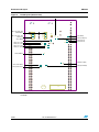
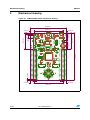
Figure 2 illustrates the connections between the STM32F303VCT6 and its peripherals
(ST-LINK/V2, pushbutton, LED, USB, Gyroscope ST MEMS, E-compass with accelerometer
ST MEMS, and connectors).
Figure 2 and Figure 3 help you to locate these features on the STM32F3DISCOVERY.
Figure 2.
Hardware block diagram
-INI53"
37$
%MBEDDED
34,).+6
34-&6#4
)/
)/
2%3%4
,%$S
,$,$
"
2%3%4
,'$
"
53%2
,3-$,(#
-INI53"
8/36
Doc ID 023594 Rev 3
(EADER
(EADER
)/
UM1570
Figure 3.
Hardware and layout
Board layout (top view)
,$REDGREEN,%$
#/-
34,).+6
53"53%2
,$RED,%$
072
#.
37$CONNECTOR
#.
34,).+
$)3#/6%29
SELECTOR
*0)$$
MEASUREMENT
,3-$,(#
6POWER
SUPPLY
INPUTOUTPUT
6POWER
SUPPLY
INPUTOUTPUT
34-&6#4
,'$
"USERBUTTON
"RESET
BUTTON
RED,%$,$
BLUE,%$,$
ORANGE,%$,$
GREEN,%$,$
GREEN,%$,$
BLUE,%$,$
ORANGE,%$,$
RED,%$,$
Note:
Pin 1 of CN3, CN4, JP3, JP4, P1 and P2 connectors are identified by a square.
Doc ID 023594 Rev 3
9/36
Hardware and layout
Figure 4.
UM1570
Board layout (bottom view)
3"37/
3"3"3"3"
2%3%26%$
3"3"3"3"
$%&!5,4
3".234
3"34-?234
3"-#/
3"2848
3"2848
3"8CRYSTAL
3"8CRYSTAL
3"8CRYSTAL
3"8CRYSTAL
3""//4
3""53%2
3"53"53%2
3""2%3%4
3"53"53%2
RoHS
Note:
10/36
SN
If SB12 is ON, SB17 must be OFF and R33 removed to provide the clock source from MCO
correctly.
Doc ID 023594 Rev 3
UM1570
4.1
Hardware and layout
STM32F303VCT6 microcontroller
This ARM™Cortex-M4 32-bit MCU with FPU has 256 KB Flash, 48 KB SRAM, 4 ADCs, two
DAC channels, seven comparators, four PGAs, 13 timers, 2.0-3.6 V operation.
Figure 5.
STM32F303VCT6 package
34-&6#4
+BYTESOF&LASHMEMORY
+BYTESOF32!-
,1&0XMM
-36
This device provides the following benefits.
●
●
72 MHz/62 DMIPS (from Flash) or 94 DMIPS (from CCM-SRAM) Cortex-M4 with single
cycle DSP MAC and floating point unit:
–
Boosted execution of control algorithms.
–
More features possible for your applications.
–
Ease of use.
–
Better code efficiency.
–
Faster time to market.
–
Elimination of scaling and saturation.
–
Easier support for meta-language tools.
Real-time performance:
–
CCM-SRAM (core coupled memory): 8 Kbytes of SRAM mapped to the instruction
bus; critical routines loaded in the 8-Kbyte CCM at startup can be completed at full
speed with zero wait states, achieving 94 Dhrystone MIPS and CoreMark score
155 at 72 MHz.
–
SRAM and CCM-SRAM with parity bit
–
32-bit AHB bus matrix
–
DMA controllers
–
Memory protection unit (MPU).
More performance for critical routines with zero-wait state execution from safe CCMSRAM.
●
Outstanding power efficiency:
–
Stop mode down to 5.7 μA typ
–
RTC <2 μA typ in VBAT mode
–
2.0 to 3.6 V or 1.8 V +/-8% power supply range
–
Flexibility to reduce power consumption for applications requiring advanced
analog peripherals and low-power modes.
–
Running at low voltage or on a rechargeable battery.
Doc ID 023594 Rev 3
11/36
Hardware and layout
●
Maximum integration:
–
●
●
12/36
UM1570
Up to 256 Kbytes of on-chip Flash memory, 48 Kbytes of SRAM, reset circuit,
internal RCs, PLLs, more features in space-constrained applications.
Superior and innovative peripherals:
–
Analog: 4x 12-bit ADC 5 MSPS reaching 18 MSPS in interleaved mode, fast
comparators (50 ns), programmable gain amplifiers (4 gains, 1% accuracy). 12-bit
DACs.
–
Up to 13 timers: one 32-bit (TIM2) and 12 16-bit timers, running up to 144 MHz
(TIM1,8) or 72 MHz.
–
Audio: simplex or full duplex I²S interfaces.
–
Up to 12 communication interfaces including 5x USART (9 Mbit/s),
3x SPIs/2x I2Ss (18 Mbit/s), 2x I2C (1 MHz fast mode plus), CAN (1 Mbit/s), USB
full speed.
–
Cyclic redundancy check (CRC).
–
Capacitive touch-sensing (24 keys).
–
Full set of integration features on chip resulting in simplified board designs and
fewer external components.
–
BOM cost reduced.
Pin compatibility and same API for peripherals as F1 series:
–
More than 350 Cortex-M based compatible STM32 devices.
–
More than 70 Cortex-M4 based compatible STM32 devices.
–
Digital signal processing (DSP) capability at a competitive price.
Doc ID 023594 Rev 3
UM1570
Hardware and layout
STM32F303VCT6 block diagram
6$$)/
6OLTAGEREG
6TO6
-05&05
)BUS
#ORTEX-#05
3YSTEM
0/2
2ESET
)NT
##-2!+"
3UPPLY
3UPERVISION
.2%3%4
6 $$!
6 33!
0/20$2
06$
32!+"
6$$!
6$$!
6$$)/
2#(3-(Z
'0$-!
CHANNELS
TO6
V33
6$$)/
&,!3(+"
BITS
$BUS
& MAX -(Z
.6)#
0OWER
6$$
%44RACE4RIG
/",
37*4!'
&LASH
INTERFACE
40)5
42!$%#,+
42!#%$;=
AS!&
*4234
*4$)
*4#+37#,+
*4-337$!4
*4$/
!S!&
"US-ATRIX
Figure 6.
2#,3
/3#?).
/3#?/54
84!,/3#
-(Z
0,,
'0$-!
CHANNELS
)ND7$'+
!("0#,+
4EMPSENSOR
6 2%&
BIT!$#
!0"0#,+
)&
'0)/0/24!
0";=
'0)/0/24"
0#;=
'0)/0/24#
0$;=
'0)/0/24$
0%;=
'0)/0/24%
0&;=
'0)/0/24&
84!,K(Z
"ACKUP
24#
2EG
!75 "YTE
"ACKUP
INTERFACE
53!24#,+
)##,+
!$#3!2
#,+
#2#
4OUCH3ENSING
#ONTROLLER
!("
!0"
%84)4
7+50
4)-%2
#HANNELS%42AS!&
4)-%2
#HANNELS%42AS!&
30))3
-/3)3$-)3/EXT?3$
3#+#+.3373-#,+AS!&
30))3
-/3)3$-)3/EXT?3$
3#+#+.3373-#,+AS!&
53!24
2848#43243AS!&
53!24
2848#43243AS!&
!("
!0"
4)-%2
#HANNEL#OMP
#HANNEL"2+AS!&
4)-%2
#HANNELS
#OMPCHANNELS
%42"2+AS!&
#HANNELS
#OMPCHANNELS
%42"2+AS!&
4)-%207-
4)-%2
2848#43243
3MART#ARDAS!&
53!24
2848AS!&
)#
3#,3$!3-"!,AS!&
)#
3#,3$!3-"!,AS!&
#!.48#!.28
53"&3
53"$053"$-
$!#?#(AS!&
)& BIT$!#
$!#?#(AS!&
6$$!
393#&'#4,
30)
5!24
4)-%2
4)-%207-
-/3)-)3/
3#+.33AS!&
2848AS!&
BX#!.
"32!-
).4%2&!#%
4)-%2
#HANNEL#OMP
#HANNEL"2+AS!&
5!24
53"32!-"
!0"F MAX-(Z
#HANNELS#OMP
#HANNEL"2+AS!&
!.4)4!-0
#HANNELS%42AS!&
7IN7!4#($/'
88!&
/3#?).
/3#?/54
4)-%2
BIT07-
!0"& MAX -(Z
0!;=
88'ROUPSOF
CHANNELSAS!&
&#,+
)&
AHB decoder
BIT!$#
6"!4 6TO6
637
(#,+
2ESET
CLOCK
CONTROL
6 2%&
BIT!$#
3TANDBY
INTERFACE
!0"0#,+
BIT!$#
/P!MP
).XX/54XX
/P!MP
).XX/54XX
/P!MP
).XX/54XX
/P!MP
).XX/54XX
6$$!
'0#OMPARATOR
6$$!
'0#OMPARATOR
'0#OMPARATOR
8X)NS/54SAS!&
Doc ID 023594 Rev 3
MS18960V4
13/36
Hardware and layout
4.2
UM1570
Embedded ST-LINK/V2
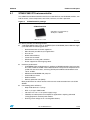
The ST-LINK/V2 programming and debugging tool is integrated on the
STM32F3DISCOVERY. The embedded ST-LINK/V2 can be used in two different ways
according to the jumper states (Table 3).
●
Program/debug the MCU on board,
●
Program/debug an MCU in an external application board using a cable connected to
SWD connector CN3.
The embedded ST-LINK/V2 supports only SWD for STM32 devices. For information about
debugging and programming features, refer to user manual UM1075 (ST-LINK/V2 in-circuit
debugger/programmer for STM8 and STM32) which describes in detail all the ST-LINK/V2
features.
Figure 7.
Typical configuration
Hardware requirements:
- USB cable type A to mini-B
- Computer with Windows XP, Vista or 7
Development toolchains:
- Altium TASKING VX-Toolset
- Atollic TrueSTUDIO
- IAR EWARM
- Keil MDK-ARM
MS31115V1
Table 3.
Jumper states
Jumper state
4.2.1
Description
Both CN4 jumpers ON
ST-LINK/V2 functions enabled for on-board programming (default)
Both CN4 jumpers OFF
ST-LINK/V2 functions enabled for application through external CN3
connector (SWD supported)
Using ST-LINK/V2 to program/debug the STM32F303VCT6 on board
To program the STM32F303VCT6 MCU on the board, simply plug in the two jumpers on
CN4, as shown in Figure 8 in red, but do not use the CN3 connector as that could disturb
communication with the STM32F303VCT6 of the STM32F3DISCOVERY.
14/36
Doc ID 023594 Rev 3
UM1570
Hardware and layout
Figure 8.
4.2.2
STM32F3DISCOVERY connections image
Using ST-LINK/V2 to program/debug an external STM32 application
It is very easy to use the ST-LINK/V2 to program the STM32 on an external application.
Simply remove the two jumpers from CN4 as shown in Figure 9, and connect your
application to the CN3 debug connector according to Table 4.
Note:
SB7 must be OFF if you use the CN3 pin 5 in your external application.
Table 4.
Debug connector CN3 (SWD)
Pin
CN3
Designation
1
VDD_TARGET
VDD from application
2
SWCLK
SWD clock
3
GND
Ground
4
SWDIO
SWD data input/output
5
NRST
RESET of target MCU
6
SWO
Reserved
Doc ID 023594 Rev 3
15/36
Hardware and layout
Figure 9.
16/36
UM1570
ST-LINK/V2 connections image
Doc ID 023594 Rev 3
UM1570
4.3
Hardware and layout
Power supply and power selection
The power supply is provided either by the host PC through the USB cable, or by an external
5 V power supply.
The D1 and D2 diodes protect the 5 V and 3 V pins from external power supplies.
●
5 V and 3 V can be used as output power supplies when another application board is
connected to pins P1 and P2. In this case, the 5 V and 3 V pins deliver a 5 V or 3 V
power supply and power consumption must be lower than 100 mA.
●
5 V and 3 V can also be used as input power supplies, for example when the USB
connectors are not connected to the PC. In this case, the STM32F3DISCOVERY board
must be powered by a power supply unit or by auxiliary equipment complying with
standard EN-60950-1: 2006+A11/2009, and must be safety extra low voltage (SELV)
with limited power capability.
Note:
The board can be also powered through the USB USER connector and is protected by D4
and D5 diodes when both USBs are connected (in which case, the 5 V power is around 4.4
volts).
4.4
LEDs
4.5
●
LD1 PWR: red LED indicates that the board is powered.
●
LD2 COM: LD2 default status is red. LD2 turns to green to indicate that
communications are in progress between the PC and the ST-LINK/V2.
●
User LD3: red LED is a user LED connected to the I/O PE9 of the STM32F303VCT6.
●
User LD4: blue LED is a user LED connected to the I/O PE8 of the STM32F303VCT6.
●
User LD5: orange LED is a user LED connected to the I/O PE10 of the
STM32F303VCT6.
●
User LD6: green LED is a user LED connected to the I/O PE15 of the
STM32F303VCT6.
●
User LD7: green LED is a user LED connected to the I/O PE11 of the
STM32F303VCT6.
●
User LD8: orange LED is a user LED connected to the I/O PE14 of the
STM32F303VCT6.
●
User LD9: blue LED is a user LED connected to the I/O PE12 of the STM32F303VCT6.
●
User LD10: red LED is a user LED connected to the I/O PE13 of the STM32F303VCT6.
Pushbuttons
●
B1 USER: user and wake-up button connected to the I/O PA0 of the STM32F303VCT6.
●
B2 RESET: pushbutton connected to NRST is used to RESET the STM32F303VCT6.
Doc ID 023594 Rev 3
17/36
Hardware and layout
4.6
UM1570
USB device supported
The STM32F303VCT6 MCU is also used to drive the second USB mini-B connector (USB
USER) which allows the board to be used as a USB Device. The STM32F3DISCOVERY
can then act as a USB joystick, mouse, or other similar device. If both USBs are connected,
diodes D4 and D5 protect the board and use the power from the USB ST-LINK.
The board can be powered through this USB USER connector, then LED1 PWR lights,
LED2 COM blinks and it can run an application in standalone mode.
4.7
E-compass/accelerometer MEMS (ST MEMS LSM303DLHC)
The LSM303DLHC is an ultra-compact low-power system-in-package featuring a 3D digital
linear acceleration sensor and a 3D digital magnetic sensor. It includes a sensing element
and an IC interface able to provide the measured acceleration to the external world through
I2C serial interface.
The LSM303DLHC has dynamically user-selectable full scales of ±2g/±8g and is capable of
measuring acceleration, and a magnetic field full scale from ±1.3g to 8.1g with an output
data rate of 100 Hz or 400 Hz.
The STM32F303VCT6 MCU controls this motion sensor through the I2C interface.
4.8
Gyroscope MEMS (ST MEMS L3GD20)
The L3GD20 is an ultra-compact, low-power, three-axis angular rate sensor. It includes a
sensing element and an IC interface able to provide the measured angular rate to the
external world through the I2C/SPI serial interface.
The L3GD20 has dynamically user-selectable full scales of ±250 dps/±500 dps/±2000 dps
and is capable of measuring rates.
The STM32F303VCT6 MCU controls this motion sensor through the SPI interface.
4.9
JP3 (Idd)
Jumper JP3, labeled Idd, allows the consumption of the STM32F303VCT6 to be measured
by removing the jumper and connecting an ammeter.
18/36
●
Jumper on: STM32F303VCT6 is powered (default).
●
Jumper off: an ammeter must be connected to measure the STM32F303VCT6 current.
If there is no ammeter, the STM32F303VCT6 is not powered.
Doc ID 023594 Rev 3
UM1570
Hardware and layout
4.10
OSC clock
4.10.1
OSC clock supply
The following information indicates all configurations for clock supply selection.
●
●
●
●
4.10.2
MCO from ST-LINK. From MCO of the STM32F103C8T6. This frequency cannot be
changed, it is fixed at 8 MHz and connected to PF0-OSC_IN of the STM32F303VCT6.
Configuration needed:
–
SB12 closed, SB17 open, R33 removed
–
SB18, R32, C22, C23, X2 = don't care
Oscillator on board. From X2 crystal (not provided). For typical frequencies and its
capacitors and resistors, please refer to the STM32F303VCT6 Datasheet.
Configuration needed:
–
SB12, SB17, SB18 open
–
R32, R33, C22, C23, X2 soldered
Oscillator from external PF0. From external oscillator through pin 5 of the P2
connector. Configuration needed:
–
SB12 open, SB17 closed, R33 removed
–
SB18, R32, C22, C23, X2 = don't care
No external oscillator. From Internal oscillator HSI only. PF0 and PF1 can be used as
GPIO. Configuration needed:
–
SB12 open, SB17 closed, SB18 closed, R32 removed, R33 removed
–
C22, C23, X2 = don't care
OSC 32 kHz clock supply
The following information indicates all configurations for the 32 kHz clock supply selection.
●
●
●
Oscillator on board. From X3 Crystal (not provided). Configuration needed:
–
SB14 open, SB16 open.
–
R29, R30, C14, C26, X3 soldered.
Oscillator from external PC14. From external oscillator through the pin 7 of P2
connector. Configuration needed:
–
SB14 open, R29 removed
–
SB16, R30, C14, C26, X3 = don't care
No external oscillator. PC14 and PC15 can be used as GPIO. Configuration needed:
–
SB14 closed, SB16 closed, R29 removed, R30 removed.
–
C14, C26, X3 = don't care.
Doc ID 023594 Rev 3
19/36
Hardware and layout
UM1570
4.11
Solder bridges
Table 5.
Solder bridges
State(1)
Description
SB17,18
(X1 crystal) (2)
OFF
X1, C22, C23, R32 and R33 provide a clock. PF0, PF1 are disconnected from P2.
ON
PF0, PF1 are connected to P2 (R32 and R33 must not be fitted).
SB1,3,5,8 (default)
ON
Reserved, do not modify
SB2,4,6,9 (reserved)
OFF
Reserved, do not modify
SB14,16
(X3 crystal)
OFF
X3, C14, C26, R29 and R30 deliver a 32 KHz clock. PC14, PC15 are not
connected to P2.
ON
PC14, PC15 are only connected to P2. Remove only R26, R29
SB23
(B2-RESET)
ON
B2 Push Button is connected to NRST of STM32F303VCT6
OFF
B2 Push Button is not connected to NRST of STM32F303VCT6
ON
B1 Push Button is connected to PA0
OFF
B1 Push Button is not connected to PA0
SB13,15
(RX,TX)
OFF
Reserved, do not modify
ON
Reserved, do not modify
SB7
(NRST)
ON
NRST signal of connector CN3 is connected to NRST of STM32F303VCT6
OFF
NRST signal is not connected
ON
SWO signal of connector CN3 is connected to PB3
OFF
SWO signal is not connected
OFF
No incidence on NRST signal of STM32F103C8T6
ON
NRST signal of STM32F103C8T6 is connected to GND
ON
BOOT0 signal of STM32F303VCT6 is at level "0" through 510 ohm pull-down
OFF
BOOT0 signal of STM32F303VCT6 is at level "1" through 10K ohm pull-up (not
provided).
OFF
PA11 and PA12 are only used for USB USER and not connected to P2 to avoid
noise.
ON
PA11 and PA12 are connected to P2.
OFF
MCO signal of STM32F103C8T6 is not used.
ON
MCO clock signal from STM32F103C8T6 is connected to OSC_IN of
STM32F303VCT6.
Bridge
SB20
(B1-USER)
SB10
(SWO)
SB11
(STM_RST)
SB19
(BOOT0)
SB21,22
(USB USER)
SB12
(MCO)(2)
1. Default state is shown in bold.
2. If SB12 is ON, SB17 must be OFF and R33 removed to provide the clock source from the MCO correctly.
20/36
Doc ID 023594 Rev 3
UM1570
4.12
Hardware and layout
Extension connectors
The male headers P1 and P2 can connect the STM32F3DISCOVERY to a standard
prototyping/wrapping board. STM32F303VCT6 GPI/Os are available on these connectors.
P1 and P2 can also be probed by an oscilloscope, logical analyzer or voltmeter.
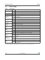
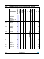
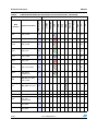
STM32F303VCT6 MCU pin description versus board function
23
PA1
TIM2_CH2, G1_IO2,
USART2_RTS,
TIM15_CH1N
24
9
PA2
TIM2_CH3, G1_IO3,
USART2_TX,
COMP2_OUT,
TIM15_CH1,
AOP1_OUT
25
14
PA3
TIM2_CH4, G1_IO4,
USART2_RX,
TIM15_CH2
26
11
PA4
TIM3_CH2, G2_IO1,
SPI1_NSS,
SPI3_NSS/I2S3_WS,
USART2_CK
29
16
PA5
TIM2_CH1_ETR,
G2_IO2, SPI1_SCK
30
Doc ID 023594 Rev 3
NRST
PA0
TIM2_CH1_ETR,
G1_IO1,
USART2_CTS,
COMP1_OUT,
TIM8_BKIN,
TM8_ETR
SCL/SPC
14
NRST
P2
P1
CN3
Power supply
Free I/O
OSC
USB
LED
Pushbutton
19
RESET
94
USER
BOOT0
L3GD20
Alternate functions
LSM303DLHC
Main
function
Board function
LQFP100 pin num.
MCU pin
SWD
Table 6.
5
4
12
15
21/36
Hardware and layout
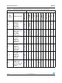
STM32F303VCT6 MCU pin description versus board function (continued)
P2
P1
CN3
Power supply
Free I/O
OSC
USB
LED
Pushbutton
31
SAO/SDO
L3GD20
PA6
TIM16_CH1,
TIM3_CH1, G2_IO3,
TIM8_BKIN,
SPI1_MISO,
TIM1_BKIN,
AOP2_OUT,
COMP1_OUT
18
PA7
TIM17_CH1,
TIM3_CH2, G2_IO4,
TIM8_CH1N,
SPI1_MOSI,
TIM1_CH1N,
COMP2_OUT
32
SDA/SDI/SDO
Alternate functions
LSM303DLHC
Main
function
Board function
LQFP100 pin num.
MCU pin
SWD
Table 6.
UM1570
17
PA8
MCO, I2C2_SMBAL,
I2S2_MCK,
TIM1_CH1,
USART1_CK,
COMP3_OUT,
TIM4_ETR
67
45
PA9
G4_IO1, I2C2_SCL,
I2S3_MCK,
TIM1_CH2,
USART1_TX,
COMP5_OUT,
TIM15_BKIN,
TIM2_CH3
68
44
PA10
TIM17_BKIN, G4_IO2,
I2C2_SDA,
TIM1_CH3,
USART1_RX,
COMP6_OUT,
TIM2_CH4,
TIM8_BKIN
69
43
PA11
TIM1_CH1N,
USART1_CTS,
COMP1_OUT,
CAN_RX, TIM4_CH1,
TIM1_CH4_BKIN2,
USBDM
70
22/36
DM
Doc ID 023594 Rev 3
42
UM1570
STM32F303VCT6 MCU pin description versus board function (continued)
Board function
35
22
PB1
TIM3_CH4, G3_IO3,
TIM8_CH3N,
TIM1_CH3N,
COMP4_OUT,
AOP3_OUT
36
21
PB2
G3_IO4
37
24
PB3
JTDO/TRACESWO,
TIM2_CH2,
TIM4_ETR, G5_IO1,
TIM8_CH1N,
SPI1_SCK,
SPI3_SCK/I2S3_CK,
USART2_TX,
TIM3_ETR
89
P1
TIM3_CH3, G3_IO2,
TIM8_CH2N,
TIM1_CH2N
CN3
PB0
Power supply
77
Free I/O
PA15
JTDI,
TIM2_CH1_ETR,
TIM8_CH1,
I2C1_SCL, SPI1_NSS,
SPI3_NSS/I2S3_WS,
USART2_RX,
TIM1_BKIN
OSC
76
USB
PA14
JTCK-SWCLK,
G4_IO4, I2C1_SDA,
TIM8_CH2,
TIM1_BKIN,
USART2_TX
SWD
72
LED
PA13
JTMS-SWDAT,
TIM16_CH1N,
G4_IO3, IR-Out,
USART3_CTS,
TIM4_CH3
Pushbutton
71
L3GD20
PA12
TIM16_CH1,
TIM1_CH2N,
USART1_RTS,
COMP2_OUT,
CAN_TX, TIM4_CH2,
TIM1_ETR, USBDP
SWDIO
41
4
40
SWCLK
DP
2
37
38
SWO
Main
function
LSM303DLHC
Alternate functions
LQFP100 pin num.
MCU pin
P2
Table 6.
Hardware and layout
Doc ID 023594 Rev 3
6
26
23/36
Hardware and layout
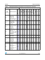
Table 6.
UM1570
STM32F303VCT6 MCU pin description versus board function (continued)
22
PB8
TIM16_CH1,
TIM4_CH3, SYNCH,
I2C1_SCL,
COMP1_OUT,
CAN_RX, TIM8_CH2,
TIM1_BKIN
95
17
PB9
TIM17_CH1,
TIM4_CH4,
I2C1_SDA, IR-OUT,
CAN_TX, TIM8_CH3
96
18
PB10
TIM2_CH3, SYNCH,
USART3_TX
47
34
PB11
TIM2_CH4, G6_IO1,
USART3_RX,
COMP2_OUT
48
33
24/36
Doc ID 023594 Rev 3
P2
93
P1
PB7
TIM17_CH1N,
TIM4_CH2, G5_IO4,
I2C1_SDA,
TIM8_BKIN,
USART1_RX,
TIM3_CH4
CN3
SCL
21
Power supply
92
Free I/O
PB6
TIM16_CH1N,
TIM4_CH1, G5_IO3,
I2C1_SCL,
TIM8_CH1,
TIM8_ETR_BKIN2,
USART1_TX
OSC
24
USB
91
SWD
PB5
TIM16_BKIN,
TIM3_CH2,
TIM8_CH3N,
I2C1_SMBAL,
SPI1_MOSI,
SPI3_MOSI/I2S3_DO
UT, USART2_CK,
TIM17_CH1
LED
23
Pushbutton
90
L3GD20
PB4
NJTRST, TIM16_CH1,
TIM3_CH1, G5_IO2,
TIM8_CH2N,
SPI1_MISO,
SPI3_MISO/I2S3_DIN,
USART2_RX,
TIM17_BKIN
Main
function
LSM303DLHC
Alternate functions
SDA
Board function
LQFP100 pin num.
MCU pin
UM1570
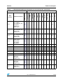
STM32F303VCT6 MCU pin description versus board function (continued)
Board function
54
37
PC0
15
6
PC1
16
5
P1
PB15
TIM15_CH2,
TIM15_CH1N,
TIM1_CH3N,
SPI2_MOSI/
I2S2_DOUT
CN3
38
Power supply
53
Free I/O
PB14
TIM15_CH1, G6_IO4,
SPI2_MISO/I2S2_DIN,
TIM1_CH2N,
USART3_RTS
OSC
35
USB
52
SWD
PB13
G6_IO3,
SPI2_SCK/I2S2_CK,
TIM1_CH1N,
USART3_CTS
LED
36
Pushbutton
51
L3GD20
PB12
G6_IO2,
I2C2_SMBAL,
SPI2_NSS/I2S2_WS,
TIM1_BKIN,
USART3_CK,
AOP4_OUT
Main
function
LSM303DLHC
Alternate functions
LQFP100 pin num.
MCU pin
PC2
COMP7_OUT
17
8
PC3
TIM1_BKIN2
18
7
PC4
USART1_TX
33
20
PC5
G3_IO1, USART1_RX
34
19
PC6
TIM3_CH1,
TIM8_CH1,
I2S2_MCK,
COMP6_OUT
63
47
PC7
TIM3_CH2,
TIM8_CH2,
I2S3_MCK,
COMP5_OUT
64
48
PC8
TIM3_CH3,
TIM8_CH3,
COMP3_OUT
65
P2
Table 6.
Hardware and layout
47
Doc ID 023594 Rev 3
25/36
Hardware and layout
STM32F303VCT6 MCU pin description versus board function (continued)
P2
P1
CN3
Power supply
Free I/O
OSC
USB
LED
Pushbutton
L3GD20
Alternate functions
LSM303DLHC
Main
function
Board function
LQFP100 pin num.
MCU pin
SWD
Table 6.
UM1570
TIM3_CH4,
TIM8_CH4_BKIN2,
COMP3_OUT
66
46
PC10
TIM8_CH1N,
UART4_TX,
SPI3_SCK/I2S3_CK,
USART3_TX
78
35
PC11
TIM8_CH2N,
UART4_RX,
SPI3_MISO/I2S3_DIN,
USART3_RX
79
36
PC12
TIM8_CH3N,
UART5_TX,
SPI3_MOSI/
I2S3_DOUT,
USART3_CK
80
33
PC13
TIM1_CH1N
7
10
PC14
OSC32_IN
8
PC15
OSC32_OUT
9
PD0
CAN_RX
81
34
PD1
TIM8_CH4_BKIN2,
CAN_TX
82
31
PD2
TIM3_ETR,
TIM8_BKIN,
UART5__RX
83
32
PD3
TIM2_CH1_ETR,
USART2_CTS
84
29
PD4
TIM2_CH2,
USART2_RTS
85
30
PD5
USRT2_TX
86
27
26/36
OSC32_OUT OSC32_IN
PC9
Doc ID 023594 Rev 3
7
8
UM1570
STM32F303VCT6 MCU pin description versus board function (continued)
P2
P1
CN3
Power supply
Free I/O
OSC
USB
LED
Pushbutton
87
28
PD7
TIM2_CH3,
USART2_CK
88
25
PD8
USART3_TX
55
40
PD9
USART3_RX
56
39
PD10
USART3_CK
57
42
PD11
USART3_CTS
58
41
PD12
TIM4_CH1, G8_IO1,
USART3_RTS
59
44
PD13
TIM4_CH2, G8_IO2
60
43
PD14
TIM4_CH3, G8_IO3
61
46
PD15
TIM4_CH4, G8_IO4,
SPI2_NSS
62
45
PE0
TIM4_ETR,
TIM16_CH1,
USART1_TX
97
INT1
L3GD20
TIM2_CH4,
USART2_RX
15
PE1
TIM17_CH1,
USART1_RX
98
16
PE2
TRACECK,
TIM3_CH1, G7_IO1
1
PE3
TRACED0,
TIM3_CH2, G7_IO2
2
PE4
TRACED1,
TIM3_CH3, G7_IO3
3
PE5
TRACED2,
TIM3_CH4, G7_IO4
4
PE6
TRACED3
5
PE7
TIM1_ETR
38
DRDY
PD6
DRDY/INT2
Alternate functions
LSM303DLHC
Main
function
Board function
LQFP100 pin num.
MCU pin
SWD
Table 6.
Hardware and layout
CS_I2C/SPI
13
INT2 INT1
14
11
12
9
23
Doc ID 023594 Rev 3
27/36
Hardware and layout
STM32F303VCT6 MCU pin description versus board function (continued)
39
PE9
TIM1_CH1
40
PE10
TIM1_CH2N
41
PE11
TIM1_CH2
42
PE12
TIM1_CH3N
43
PE13
TIM1_CH3
44
PE14
TIM1_CH4_BKIN2
45
PE15
TIM1_BKIN,
USART3_RX
46
PF0
OSC_IN, I2C2_SDA,
TIM1_CH3N
12
PF1
OSC_OUT, I2C2_SCL
13
PF2
P2
P1
CN3
Power supply
Free I/O
USB
LED
Pushbutton
OSC
26
25
28
27
30
29
32
31
OSC_OUT OSC_IN
TIM1_CH1N
LD6/
LD8/
LD10/ LD9/
LD7/
LD5/
LD3/ LD4/
GREEN ORANGE RED BLUE GREEN ORANGE RED BLUE
PE8
L3GD20
Alternate functions
LSM303DLHC
Main
function
Board function
LQFP100 pin num.
MCU pin
SWD
Table 6.
UM1570
5
6
19
10
13
PF4
COMP1_OUT
27
PF6
TIM4_CH4,
I2C2_SCL,
USART3_RTS
73
39
PF9
TIM15_CH1,
SPI2_SCK
10
3
PF10
TIM15_CH2,
SPI2_SCK
11
4
28/36
Doc ID 023594 Rev 3
UM1570
STM32F303VCT6 MCU pin description versus board function (continued)
Doc ID 023594 Rev 3
P2
P1
CN3
Power supply
5V
1
5V
2
3V
1
3V
2
GND GND GND VDD
Free I/O
OSC
USB
LED
Pushbutton
L3GD20
Alternate functions
LSM303DLHC
Main
function
Board function
LQFP100 pin num.
MCU pin
SWD
Table 6.
Hardware and layout
20
3
49
49
50
50
29/36
Mechanical drawing
5
UM1570
Mechanical drawing
Figure 10. STM32F3DISCOVERY mechanical drawing
66.00mm
53.34mm
2.22mm
97.00mm
15.24mm
33.82mm
16.04mm
6.33mm
5.08mm
33.82mm
3.34mm
6.33mm
2.54mm
6.33mm
30/36
2.54mm
53.34mm
Doc ID 023594 Rev 3
6.33mm
STM32F3DISCOVERY electrical schematics
UM1570
6
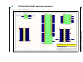
Figure 11. STM32F3DISCOVERY top level
1
2
3
ST_LINK_V2.SCHDOC
U_ST_LINK
PC5
PC4
STM32F3_USART1_RX
STM32F3_USART1_TX
PC5
PC4
A
MCO
PA14
PA13
PB3
NRST
U_STM32Fx
STM32Fx.SchDoc
MCO
PA14
PA13
PB3
TCK/SWCLK
TMS/SWDIO
T_SWO
NRST
T_NRST
PA0
PA1
PA2
PA3
PA4
PA5
PA6
PA7
PA8
PA9
PA10
PA11
PA12
PA13
PA14
PA15
P1
3V
C
1
3
5
7
9
11
13
15
17
19
21
23
25
27
29
31
33
35
37
39
41
43
45
47
49
PC1
PC3
PA1
PA3
PF4
PA5
PA7
PC5
PB1
PE7
PE9
PE11
PE13
PE15
PB11
PB13
PB15
PD9
PD11
PD13
PD15
PC6
2
4
6
8
10
12
14
16
18
20
22
24
26
28
30
32
34
36
38
40
42
44
46
48
50
3V
NRST
PC0
PC2
PF2
PA0
PA2
PA4
PA6
PC4
PB0
PB2
PE8
PE10
PE12
PE14
PB10
PB12
PB14
PD8
PD10
PD12
PD14
PC7
3V
PC0
PC1
PC2
PC3
PC4
PC5
PC6
PC7
PC8
PC9
PC10
PC11
PC12
PC13
PC14
PC15
BOOT0
Header 25X2
NRST
U_IO Peripherals
IO Peripherals.SchDoc
PA0
PA1
PA2
PA3
PA4
PA5
PA6
PA7
PA8
PA9
PA10
PA11
PA12
PA13
PA14
PA15
PE0
PE1
PE2
PE3
PE4
PE5
PE6
PE7
PE8
PE9
PE10
PE11
PE12
PE13
PE14
PE15
PB0
PB1
PB2
PB3
PB4
PB5
PB6
PB7
PB8
PB9
PB10
PB11
PB12
PB13
PB14
PB15
PD0
PD1
PD2
PD3
PD4
PD5
PD6
PD7
PD8
PD9
PD10
PD11
PD12
PD13
PD14
PD15
PC0
PC1
PC2
PC3
PC4
PC5
PC6
PC7
PC8
PC9
PC10
PC11
PC12
PC13
PC14
PC15
PF0
PF1
PF2
PF4
PF6
PF9
PF10
PE0
PE1
PE2
PE3
PE4
PE5
PE6
PE7
PE8
PE9
PE10
PE11
PE12
PE13
PE14
PE15
PE0
PE1
PE2
PE3
PE4
PE5
PE8
PE9
PE10
PE11
PE12
PE13
PE14
PE15
PD0
PD1
PD2
PD3
PD4
PD5
PD6
PD7
PD8
PD9
PD10
PD11
PD12
PD13
PD14
PD15
NRST
NRST
PA0
PA0
PE8
PE9
PE10
PE11
PE12
PE13
PE14
PE15
A
PA5
PA6
PA7
PA5
PA6
PA7
PA11
PA12
PA11
PA12
PB6
PB7
PB6
PB7
B
P2
5V
PF0
PF1
PF2
PF4
PF6
PF9
PF10
5V
PF9
PF0
PC14
PE6
PE4
PE2
PE0
PB8
BOOT0
PB6
PB4
PD7
PD5
PD3
PD1
PC12
PC10
PA14
PF6
PA12
SB21
MCO
PE0
PE1
PE2
PE3
PE4
PE5
MCO
BOOT0
PA10
PA8
PC8
1
3
5
7
9
11
13
15
17
19
21
23
25
27
29
31
33
35
37
39
41
43
45
47
49
5V
PF10
PF1
PC15
PC13
PE5
PE3
PE1
PB9
2
4
6
8
10
12
14
16
18
20
22
24
26
28
30
32
34
36
38
40
42
44
46
48
50
5V
VDD
PB7
PB5
PB3
PD6
PD4
PD2
PD0
PC11
PA15
PA13
C
PA11
PA9
PC9
SB22
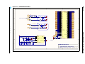
Header 25X2
NRST
Rev A.0 --> First Version
Rev B.0 --> PCB B-00, added 2 SB to isolate USB USER
Rev B.1 --> PCB B-00, reverse LEDs Colors Red/Blue on sheet 4, only a picture modification
D
D
STMicroelectronics
Title:
STM32F3DISCOVERY
31/36
Number:MB1035 Rev: B.1(PCB.SCH)
1
2
3
Date: 9/13/2012
4
Sheet 1
of
4
STM32F3DISCOVERY electrical schematics
Doc ID 023594 Rev 3
PB0
PB1
PB2
PB3
PB4
PB5
PB6
PB7
PB8
PB9
PB10
PB11
PB12
PB13
PB14
PB15
B
3V
4
1
2
3
4
TCK/SWCLK
TMS/SWDIO
PA14
PA13
NRST
PB3
T_NRST
8MHz
R23
100K
OSC_IN
OSC_OUT
STM_RST
B
C12
Doc ID 023594 Rev 3
100nF
3V
R24
4K7
R25
4K7
AIN_1
VBAT
PC13
PC14
PC15
OSCIN
OSCOUT
NRST
VSSA
VDDA
PA0
PA1
PA2
STLINK_TX
SB11
1
2
3
4
5
6
7
8
9
10
11
12
STM32F3_USART1_RX
PC5
SB13
TX
RX
JP4
STLINK_RX
PC4
VDD_2
VSS_2
JTMS/SWDIO
PA12
PA11
PA10
PA9
PA8
PB15
PB14
PB13
PB12
3V
T_JTCK
22
R20
22
R21
3V
SB2
SB3
SB4
SB5
SB6
SB8
SB9
T_NRST
22
R22
STM_JTCK
SWCLK
STM_JTMS
SWDIO
T_SWO
22
R48
RC Must be very close to STM32F103 pin 29
100
T_JTMS
T_JTCK
SB1
T_JTMS
Header 6
STM_JTMS
USB_DP
USB_DM
T_SWO
LED_STLINK
A
MCO
B
MCO
CN4
C38
20pF
R26
100
Jumpers ON --> DISCOVERY Selected
Jumpers OFF --> ST-LINK Selected
Not Fitted
T_SWDIO_IN
Wired on Solder Side
Idd
3V
3V
JP3
LD2
JP2
VDD
COM
R6
Red
2
1
100
R1
1K
SB15
STM32F3_USART1_TX
36
35
34
33
32
31
30
29
28
27
26
25
R19
1
2
3
4
5
6
U2
STM32F103C8T6
JP1
R5
LED_STLINK
3
4
R2
0
100
C
LD1
RED
PWR
D2
5V
VCC
DD+
ID
GND
SHELL
1
2
3
4
5
0
R12
R14
R13
R11
1K5
3V
0
USB_DM
0
USB_DP
100K
C10
100nF
C5
100nF
C8
100nF
Vin
Vout
5
3V
3 INH
BAT60JFILM
C3
C6
GND
BYPASS
1μF_X5R_0603
1μF_X5R_0603
EXT_3V,
LD3985M33R
C1
C2
C4
10nF_X7R_0603
100nF
100nF
C13
100nF
2
EXT_5V, Input or Output
1
3V
U5V
CN1
D3
U1
4
USB ST-LINK
BAT60JFILM
C
LD_BICOLOR_CMS
5V
U5V
3V
_Green
Not Fitted
Close to JP
Not Fitted
SWD
RESERVED
SWIM_IN
SWIM
C7
20pF
2
48
47
46
45
44
43
42
41
40
39
38
37
3V
X1
AIN_1
100
VDD_3
VSS_3
PB9
PB8
BOOT0
PB7
PB6
PB5
PB4/JNTRST
PB3/JTDO
PA15/JTDI
JTCK/SWCLK
1
R7
BAT60JFILM
PA3
PA4
PA5
PA6
PA7
PB0
PB1
PB2/BOOT1
PB10
PB11
VSS_1
VDD_1
C9
20pF
3V
D1
CN3
13
14
15
16
17
18
T_JRST 19
20
SWIM_IN 21
22
SWIM
23
24
Not Fitted
R3
10K
SWD
DEFAULT
100K
SB10
1
2
3
4
10K
Board Ident: PC13=0
T_SWO
Not Fitted
STM_JTCK
R8
R10
SWIM_IN
SWIM_RST
SWIM_RST_IN
10K
T_JTCK
T_JTDO
T_JTDI
T_NRST
A
R9
SB7
Input or Output
5075BMR-05-SM
D
D
STMicroelectronics
Title:
STM32F3DISCOVERY ST-LINK/V2 (SWD only)
Number:MB1035 Rev: B.1(PCB.SCH)
2
3
Date: 9/13/2012
4
Sheet 2
of
4
UM1570
1
STM32F3DISCOVERY electrical schematics
32/36
Figure 12. ST-LINK/V2 (SWD only)
1
2
3
UM1570
Figure 13. STM32F303VCT6 MCU
4
U4A
PA0
PA1
PA2
PA3
PA4
PA5
PA6
PA7
PA8
PA9
PA10
PA11
PA12
PA13
PA14
PA15
A
MCO
PF0
MCO
SB12
PF0-OSC_IN
R33
0
PF1-OSC_OUT
R32
220
1
Must be close to the Crystal
PF1
C23
20pF
2
SB17
X2
8MHz
C22
20pF
SB18
Not Fitted
C14
PC15-OSC32_OUT
PC15
R30
0
3
0
4
R29
SB14
2
PC14-OSC32_IN
PC14
1
B
6.8pF
X3
MC306-G-06Q-32.768
C26
SB16
Not Fitted
6.8pF
23
24
25
26
29
30
31
32
67
68
69
70
71
72
76
77
PB0
PB1
PB2
PB3
PB4
PB5
PB6
PB7
PB8
PB9
PB10
PB11
PB12
PB13
PB14
PB15
35
36
37
89
90
91
92
93
95
96
47
48
51
52
53
54
PF0-OSC_IN
PF1-OSC_OUT
PF2
PF2
PF4
PF6
C
PF9
PF10
U4B
VDD
50
75
28
L1
fcm1608-0603
C20
1uF
C21
100nF
C16
1uF
C17
100nF
100
22
R31
0
C32
100nF
C27
100nF
D
C30
100nF
21
R34
C31
100nF
C29
100nF
C28
100nF
C25
100nF
6
0
VDD2
VDD3
VDD4
VSS3
VSS2
VDDA_VDD1 VSSA_VSS1
74
49
NRST
BOOT0
VDD
R36
10K
R35
99
12
13
19
PF4
27
PF6
73
PF9
PF10
10
11
NRST
14
BOOT0
94
510
PA0 PC15-OSC32_OUT
PA1
PC14-OSC32_IN
PA2
PC13-WKUP2
PA3
PC12
PA4
PC11
PA5
PC10
PA6
PC9
PA7
PC8
PA8
PC7
PA9
PC6
PA10
PC5
PA11
PC4
PA12
PC3
PA13
PC2
PA14
PC1
PA15
PC0
PB0
PB1
PB2
PB3
PB4
PB5
PB6
PB7
PB8
PB9
PB10
PB11
PB12
PB13
PB14
PB15
PD15
PD14
PD13
PD12
PD11
PD10
PD9
PD8
PD7
PD6
PD5
PD4
PD3
PD2
PD1
PD0
PF0-OSC_IN
PF1-OSC_OUT
PF2
PF4
PF6
PF9
PF10
NRST
BOOT0
PE15
PE14
PE13
PE12
PE11
PE10
PE9
PE8
PE7
PE6-WKUP3
PE5
PE4
PE3
PE2
PE1
PE0
9
8
7
80
79
78
66
65
64
63
34
33
18
17
16
15
PC15-OSC32_OUT
PC14-OSC32_IN
PC13
PC13
PC12
PC12
PC11
PC11
PC10
PC10
PC9
PC9
PC8
PC8
PC7
PC7
PC6
PC6
PC5
PC5
PC4
PC4
PC3
PC3
PC2
PC2
PC1
PC1
PC0
PC0
62
61
60
59
58
57
56
55
88
87
86
85
84
83
82
81
PD15
PD14
PD13
PD12
PD11
PD10
PD9
PD8
PD7
PD6
PD5
PD4
PD3
PD2
PD1
PD0
46
45
44
43
42
41
40
39
38
5
4
3
2
1
98
97
PE15
PE14
PE13
PE12
PE11
PE10
PE9
PE8
PE7
PE6
PE5
PE4
PE3
PE2
PE1
PE0
A
PD15
PD14
PD13
PD12
PD11
PD10
PD9
PD8
PD7
PD6
PD5
PD4
PD3
PD2
PD1
PD0
B
PE15
PE14
PE13
PE12
PE11
PE10
PE9
PE8
PE7
PE6
PE5
PE4
PE3
PE2
PE1
PE0
C
STM32F303VCT6
SB19
VDDadc
VREF+
VSSadc/VREF-
20
Not Fitted
VBAT
STM32F303VCT6
C24
1uF
D
STMicroelectronics
Title:
STM32F3DISCOVERY - STM32F303 MCU
Number:MB1035 Rev: B.1(PCB.SCH)
1
2
3
Date: 9/13/2012
4
Sheet 3
of
4
33/36
STM32F3DISCOVERY electrical schematics
Doc ID 023594 Rev 3
PB0
PB1
PB2
PB3
PB4
PB5
PB6
PB7
PB8
PB9
PB10
PB11
PB12
PB13
PB14
PB15
PA0
PA1
PA2
PA3
PA4
PA5
PA6
PA7
PA8
PA9
PA10
PA11
PA12
PA13
PA14
PA15
1
2
3
4
VDD
BAT60JFILM
Not Fitted
CN2
R16
R18
R17
R15
1
2
3
4
5
0
VCC
DD+
ID
GND
SHELL
1K5
22
22
100K
C33
3V
USB_DM
USB_DP
PA11
PA12
100nF
PA0
PE15
R43
PE15
510
B
Doc ID 023594 Rev 3
PE14
PE13
PE12
PE11
C
PE10
PE9
PE8
R45
PE14
SB20
2
N
LD8
Orange
1
2
R
PE13
PE12
PE11
PE10
PE9
PE8
SB23
C37
R4
220K
R28
10K
PB6
PB7
PE5
PE4
O
2
100nF
RESET Button
R27
10K
PB6
PB7
PE5
PE4
B
C18
U3
1
2
3
4
5
6
7
C11
2
2
A
NRST
NRST
3V
680
B
R39
100K
330
USER & WAKE-UP Button
LD6
Green
1
LD10
Red
R46
1
680
LD9
Blue
R47
1
680
LD7
Green
R44
1
510
LD5
Orange
R42
1
680
LD3
Red
R41
1
680
LD4
Blue
R40
1
680
R38
PA0
5075BMR-05-SM
3
2
A
SW-PUSH-CMS
B2
100
3
2
BAT60JFILM
VDD
R37
5V
4
1
D5
SW-PUSH-CMS
B1
D4
4
1
USB User
VDD_IO
SCL
SDA
INT2
INT1
C1
GND
VDD
SETC
SETP
GND
GND
DRDY
NC
14
13
12
11
10
9
8
10uF
C15
220nF
STM32F3DISCOVERY electrical schematics
34/36
Figure 14. Peripherals
C19
PE2
PE2
100nF
LSM303DLHC
W
G
G
4.7uF
E
3V
U5
2
O
B
2
R
2
SPI1_SCK
SPI1_MOSI
SPI1_MISO
CS_I2C/SPI
MEMS_INT2
MEMS_INT1
PA5
PA7
PA6
PE3
PE1
PE0
S
PA5
PA7
PA6
PE3
PE1
PE0
1
2
3
4
5
6
7
8
VDD_IO
SCL/SPC
SDA/SDI/SDO
SA0/SDO
CS_I2C/SPI
DRDY/INT2
INT1
GND
VDD
VDD
C1
GND
GND
GND
GND
GND
16
15
14
13
12
11
10
9
C
C35
100nF
C36
C34
10nF/25V
10uF
L3GD20
LEDs
MEMS
Silkscreen for Gyroscope and E-compass with accelerometer
D
D
STMicroelectronics
Title:
STM32F3DISCOVERY Peripherals
Number:MB1035 Rev: B.1(PCB.SCH)
2
3
Date: 9/13/2012
4
Sheet 4
of
4
UM1570
1
UM1570
7
Revision history
Revision history
Table 7.
Document revision history
Date
Revision
Changes
10-Sep-2012
1
Initial release.
20-Sep-2012
2
Added Figure 7 on page 14 and updated Figure 14 on page 34
07-Feb-2013
3
Updated Section 4.1: STM32F303VCT6 microcontroller: removed
WLCSP package, Sigma Delta ADC, CEC, updated timers and
SPI/I²Ss.
Doc ID 023594 Rev 3
35/36
UM1570
Please Read Carefully:
Information in this document is provided solely in connection with ST products. STMicroelectronics NV and its subsidiaries (“ST”) reserve the
right to make changes, corrections, modifications or improvements, to this document, and the products and services described herein at any
time, without notice.
All ST products are sold pursuant to ST’s terms and conditions of sale.
Purchasers are solely responsible for the choice, selection and use of the ST products and services described herein, and ST assumes no
liability whatsoever relating to the choice, selection or use of the ST products and services described herein.
No license, express or implied, by estoppel or otherwise, to any intellectual property rights is granted under this document. If any part of this
document refers to any third party products or services it shall not be deemed a license grant by ST for the use of such third party products
or services, or any intellectual property contained therein or considered as a warranty covering the use in any manner whatsoever of such
third party products or services or any intellectual property contained therein.
UNLESS OTHERWISE SET FORTH IN ST’S TERMS AND CONDITIONS OF SALE ST DISCLAIMS ANY EXPRESS OR IMPLIED
WARRANTY WITH RESPECT TO THE USE AND/OR SALE OF ST PRODUCTS INCLUDING WITHOUT LIMITATION IMPLIED
WARRANTIES OF MERCHANTABILITY, FITNESS FOR A PARTICULAR PURPOSE (AND THEIR EQUIVALENTS UNDER THE LAWS
OF ANY JURISDICTION), OR INFRINGEMENT OF ANY PATENT, COPYRIGHT OR OTHER INTELLECTUAL PROPERTY RIGHT.
UNLESS EXPRESSLY APPROVED IN WRITING BY TWO AUTHORIZED ST REPRESENTATIVES, ST PRODUCTS ARE NOT
RECOMMENDED, AUTHORIZED OR WARRANTED FOR USE IN MILITARY, AIR CRAFT, SPACE, LIFE SAVING, OR LIFE SUSTAINING
APPLICATIONS, NOR IN PRODUCTS OR SYSTEMS WHERE FAILURE OR MALFUNCTION MAY RESULT IN PERSONAL INJURY,
DEATH, OR SEVERE PROPERTY OR ENVIRONMENTAL DAMAGE. ST PRODUCTS WHICH ARE NOT SPECIFIED AS "AUTOMOTIVE
GRADE" MAY ONLY BE USED IN AUTOMOTIVE APPLICATIONS AT USER’S OWN RISK.
Resale of ST products with provisions different from the statements and/or technical features set forth in this document shall immediately void
any warranty granted by ST for the ST product or service described herein and shall not create or extend in any manner whatsoever, any
liability of ST.
ST and the ST logo are trademarks or registered trademarks of ST in various countries.
Information in this document supersedes and replaces all information previously supplied.
The ST logo is a registered trademark of STMicroelectronics. All other names are the property of their respective owners.
© 2013 STMicroelectronics - All rights reserved
STMicroelectronics group of companies
Australia - Belgium - Brazil - Canada - China - Czech Republic - Finland - France - Germany - Hong Kong - India - Israel - Italy - Japan Malaysia - Malta - Morocco - Philippines - Singapore - Spain - Sweden - Switzerland - United Kingdom - United States of America
www.st.com
36/36
Doc ID 023594 Rev 3