1
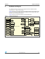
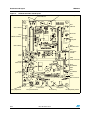
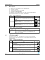
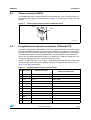
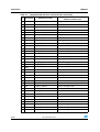
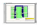
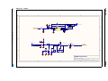
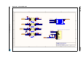
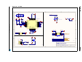
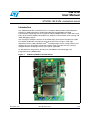
UM1018
User Manual
STM32L152-EVAL evaluation board
Introduction
The STM32L152-EVAL evaluation board is a complete demonstration and development
platform for STMicroelectronics’ ARM cortex-M3 core-based STM32L152VBT6
microcontroller supporting two I2C, two SPI and three USART channels, 12-bit ADC, 12-bit
DAC, 16 KB internal SRAM and 128 KB Flash, USB FS, LCD controller, touch sensing and
JTAG debugging support.
The full range of hardware features on the board helps you evaluate all peripherals (USB
FS, USART, Audio DAC, microphone ADC, dot-matrix LCD, LCD glass, IrDA, light
dependant resistor (LDR), MicroSD CardTM and temperature sensor amongst others) and
develop your own applications. Extension headers make it possible to easily connect a
daughter board or wrapping board for your specific application.
An ST-LINK/V2 is integrated on the board as embedded in-circuit debugger and
programmer for the STM32 MCU.
Figure 1.
November 2011
STM32L152-EVAL evaluation board
Doc ID 18141 Rev 2
1/10
www.st.com
Contents
UM01018
Contents
1
2
3
2/42
Features . . . . . . . . . . . . . . . . . . . . . . . . . . . . . . . . . . . . . . . . . . . . . . . . . . . 4
1.1
Demonstration software . . . . . . . . . . . . . . . . . . . . . . . . . . . . . . . . . . . . . . . 4
1.2
Order code . . . . . . . . . . . . . . . . . . . . . . . . . . . . . . . . . . . . . . . . . . . . . . . . . 4
Hardware and layout . . . . . . . . . . . . . . . . . . . . . . . . . . . . . . . . . . . . . . . . . 5
2.1
Development and debug support . . . . . . . . . . . . . . . . . . . . . . . . . . . . . . . . 7
2.2
Power supply . . . . . . . . . . . . . . . . . . . . . . . . . . . . . . . . . . . . . . . . . . . . . . . 7
2.3
Clock source . . . . . . . . . . . . . . . . . . . . . . . . . . . . . . . . . . . . . . . . . . . . . . . . 9
2.4
Reset source . . . . . . . . . . . . . . . . . . . . . . . . . . . . . . . . . . . . . . . . . . . . . . . 9
2.5
Boot option . . . . . . . . . . . . . . . . . . . . . . . . . . . . . . . . . . . . . . . . . . . . . . . . 10
2.6
LCD glass module . . . . . . . . . . . . . . . . . . . . . . . . . . . . . . . . . . . . . . . . . . 10
2.7
Audio . . . . . . . . . . . . . . . . . . . . . . . . . . . . . . . . . . . . . . . . . . . . . . . . . . . . 11
2.8
USB . . . . . . . . . . . . . . . . . . . . . . . . . . . . . . . . . . . . . . . . . . . . . . . . . . . . . 11
2.9
RS-232 and IrDA . . . . . . . . . . . . . . . . . . . . . . . . . . . . . . . . . . . . . . . . . . . 11
2.10
Touch sensing buttons . . . . . . . . . . . . . . . . . . . . . . . . . . . . . . . . . . . . . . . 12
2.11
MicroSD Card . . . . . . . . . . . . . . . . . . . . . . . . . . . . . . . . . . . . . . . . . . . . . . 12
2.12
Analog input . . . . . . . . . . . . . . . . . . . . . . . . . . . . . . . . . . . . . . . . . . . . . . . 12
2.13
Comparator . . . . . . . . . . . . . . . . . . . . . . . . . . . . . . . . . . . . . . . . . . . . . . . 13
2.14
Temperature sensor . . . . . . . . . . . . . . . . . . . . . . . . . . . . . . . . . . . . . . . . . 14
2.15
Display and input devices . . . . . . . . . . . . . . . . . . . . . . . . . . . . . . . . . . . . . 14
2.16
IDD measurement . . . . . . . . . . . . . . . . . . . . . . . . . . . . . . . . . . . . . . . . . . 15
2.16.1
Run mode . . . . . . . . . . . . . . . . . . . . . . . . . . . . . . . . . . . . . . . . . . . . . . . 15
2.16.2
Low power mode . . . . . . . . . . . . . . . . . . . . . . . . . . . . . . . . . . . . . . . . . . 15
2.16.3
Ibias current measurement procedure . . . . . . . . . . . . . . . . . . . . . . . . . . 17
Connectors . . . . . . . . . . . . . . . . . . . . . . . . . . . . . . . . . . . . . . . . . . . . . . . 18
3.1
RS-232 connectors (CN2, CN5) . . . . . . . . . . . . . . . . . . . . . . . . . . . . . . . . 18
3.2
TFT LCD connector (CN14) . . . . . . . . . . . . . . . . . . . . . . . . . . . . . . . . . . . 18
3.3
Power connector (CN12) . . . . . . . . . . . . . . . . . . . . . . . . . . . . . . . . . . . . . 19
3.4
Daughterboard extension connectors (CN6 and CN7) . . . . . . . . . . . . . . . 19
3.5
ST-LINK/V2 programming connector CN10 . . . . . . . . . . . . . . . . . . . . . . . 22
3.6
ST-LINK/V2 USB type B connector CN11 . . . . . . . . . . . . . . . . . . . . . . . . 23
Doc ID 18141 Rev 2
UM01018
Contents
3.7
User USB Type B connector CN1 . . . . . . . . . . . . . . . . . . . . . . . . . . . . . . 23
3.8
Audio jack CN3 . . . . . . . . . . . . . . . . . . . . . . . . . . . . . . . . . . . . . . . . . . . . . 23
3.9
JTAG connector CN9 . . . . . . . . . . . . . . . . . . . . . . . . . . . . . . . . . . . . . . . . 24
3.10
Trace debugging connector CN8 . . . . . . . . . . . . . . . . . . . . . . . . . . . . . . . 24
3.11
MicroSD Card connector CN4 . . . . . . . . . . . . . . . . . . . . . . . . . . . . . . . . . 25
3.12
BNC connector CN13 . . . . . . . . . . . . . . . . . . . . . . . . . . . . . . . . . . . . . . . . 25
4
Schematics . . . . . . . . . . . . . . . . . . . . . . . . . . . . . . . . . . . . . . . . . . . . . . . 26
5
Revision history . . . . . . . . . . . . . . . . . . . . . . . . . . . . . . . . . . . . . . . . . . . 41
Doc ID 18141 Rev 2
3/42
Features
1
UM01018
Features
●
1.1
Four 5 V power supply options:
–
Power jack
–
ST-LINK/V2 USB connector
–
User USB connector
–
Daughterboard
●
Audio speaker and microphone connected to DAC and ADC of STM32L152VBT6
●
2 GByte or more SPI interface MicroSD CardTM
●
I2C compatible serial interface temperature sensor
●
RS-232 communication
●
IrDA transceiver
●
JTAG and trace debug support, ST-LINK/V2 embedded.
●
240x320 TFT color LCD connected to SPI interface of STM32L152VBT6
●
Joystick with 4-direction control and selector
●
Reset button
●
Tamper or Key button
●
4 color user LEDs and 3 LEDs as MCU power range indicator
●
MCU consumption measurement circuit
●
LCD glass 32 x 4 segments connected to LCD controller in STM32L152VBT6
●
Extension connector for daughterboard or wrapping board
●
MCU voltage choice of 3.3 V or adjustable from 1.65 V to 3.6 V
●
USB FS connector
●
Two touch sensing buttons
●
Light dependent resistor (LDR)
●
Potentiometer
Demonstration software
Demonstration software is preloaded in the board's Flash memory for easy demonstration of
the device peripherals in stand-alone mode. For more information and to download the
latest version available, please refer to the STM32L152-EVAL demonstration software
available on www.st.com.
1.2
Order code
To order the STM32L152VBT6 evaluation board, use the order code STM32L152-EVAL.
4/42
Doc ID 18141 Rev 2
UM01018
2
Hardware and layout
Hardware and layout
The STM32L152-EVAL evaluation board is designed around the STM32L152VBT6
microcontroller in a 100-pin TQFP package.
Figure 1 illustrates the connections between the STM32L152VBT6 and its peripherals (color
LCD, touch sensing button, USB FS connector, temperature sensor, USART, IrDA, audio,
MicroSD Card and embedded ST-LINK/V2).
Figure 2 helps you to locate these features on the evaluation board.
Figure 1.
Hardware block diagram
*OYSTICK
,%$S
'0)/
7AKEUP
BUTTON
,$2
30 )
-ICRO3$
#ARD
30 )
$OT-ATRIX
,#$
6OLTAGE
TRANSLATOR
23
TRANSCEIVER
#OMPARATOR
53! 24
".#
CONNECTOR
,#$'LASS
43
CONTROLL ER
!$#
34-,6"4
!$#
,#$
CONTROLL ER
6TO6
ADJUSTABLE
REGULATOR
6REGULATOR
3PEAKER
!MPLI FIER
53" &3
*4!'
)#
%MBEDDED
34,).+6
53" 4YPE"
CONNECTOR
*4!'4RACE
CONNECTOR
-#5
CONSUMPTION
MEASUREMENT
%XTENSION
CONNECTORFOR
'0)/S
!
4EMPERATURE
SENSOR
0OTENTIOMETER
-ICROPHONE
!MPLI FIER
$!#
53"
CONNECTOR
53! 24
$"CONNECTOR
)R$!
TRANSCEIVER
&4
4OUCH
SENSING
53! 24
$"CONNECTOR
Doc ID 18141 Rev 2
5/42
Hardware and layout
Figure 2.
UM01018
STM32L152-EVAL board layout
) %
!.
!
#$%
!
5#%").
#
2/
+6 2/
&
'(
$
- %
$
5 !1
%-
,-
8%*43)
!.
!
* "!#
%"
8%*43)
%
#
.
)
)72,
6/42
$- %
)#+,
!#120/
. /0
Doc ID 18141 Rev 2
.,+ 340
UM01018
2.1
Hardware and layout
Development and debug support
Version 2 of the ST-LINK, called ST-LINK/V2, is embedded on the board. This tool allows
on-board program loading and debugging of the STM32L using the JTAG or SWD interface.
Third-party debug tools are also supported by the JTAG (CN9) or Trace (CN8) connectors.
To communicate with the embedded ST-LINK/V2, a specific driver needs to be installed on
your PC. To download and install this driver, refer to the Software and development tools
page for the ultra low power STM32L family available on www.st.com (the install shield is
called ST-LINK_V2_USBdriver.exe).
The embedded ST-LINK/V2 connects to the PC via a standard USB cable from connector
CN11. The bicolor LED LD5 (COM) advises on the status of the communication as follows:
1.
Slow blinking Red, then Off: At power-on before USB initialization.
2.
Fast blinking Red, then Off: After the first correct communication between PC and STLink/V2 (enumeration).
3.
Red On: When initialization between PC and ST-LINK/V2 is successfully finished.
4.
Green On: After successful target communication initialization.
5.
Blinking Red/Green: During communication with target.
6.
Green On: Communication finished and OK.
7.
Orange On: Communication failure.
Note:
It is possible to power the board via CN11 (embedded ST/LINK/V2 USB connector) even if
an external tool is connected to CN8 (trace) or CN9 (external JTAG and SWD).
2.2
Power supply
The STM32L152-EVAL is designed to be powered by a 5 V DC power supply and to be
protected by PolyZen from a wrong power plug-in event. It is possible to configure the
evaluation board to use any of the following four power supply sources by setting jumpers
JP12, JP13 and JP4 (see Table 1).
●
Note:
5 V DC power adapter connected to CN12, the power jack on the board (power supply
unit (PSU on silk screen)). The external power supply is not provided with the board but
can be ordered separately.
The AC220V to DC5V power adapter PSU-5V2A (recommended, can be ordered from ST
order code PSU-5V2A) or equivalent (polarity compatible with CN12) can be used to power
the STM32L152-EVAL board via its power jack CN12.
●
5 V DC power with 500 mA limitation from CN11, the USB type B connector of STLINK/V2 (USB 5 V power source (ST-LINK/V2 on silkscreen)).
●
5 V DC power with 500 mA limitation from CN1, the USB type B connector (5 V power
source (USB on silkscreen)).
●
5 V DC power from CN6, the extension connector for daughterboard (daughterboard
power source (Daughter board on JP12 silkscreen).
Various LEDs indicate the power status:
●
Red LED LD9 is lit when the STM32L152-EVAL board is powered correctly by 5 V.
●
Red LED LD8 is lit when MCU is powered by low voltage (VDD < 1.8 V).
●
Yellow LED LD7 is lit when MCU is powered by voltage (1.8 V<VDD<2.2 V).
●
Green LED LD6 is lit when MCU is powered by voltage (2.2 V<VDD).
Doc ID 18141 Rev 2
7/42
Hardware and layout
Table 1.
UM01018
Power related jumpers
Jumper
JP12
(selects one of
the four possible
power supply
resources)
Description
Jumper setting
For power supply from jack (CN12) to the STM32L152-EVAL
only, JP12 is set as shown.
PSU
Daughter
board
USB
STLink/V2
For power supply from daughterboard connector (CN6) to
STM32L152-EVAL only, JP12 is set as shown.
PSU
Daughter
board
USB
STLink/V2
For power supply from USB (CN1) to STM32L152-EVAL only,
JP12 is set as shown.
PSU
Daughter
board
USB
STLink/V2
For power supply from USB connector of ST-LINK/V2 (CN11)
to STM32L152-EVAL only, JP12 is set as shown (default
setting).
PSU
Daughter
board
USB
STLink/V2
For power supply from power supply jack (CN12) to both
STM32L152-EVAL and daughterboard connected on CN6 and
CN7, JP12 is set as shown (daughterboard must not have its
own power supply connected).
PSU
Daughter
board
USB
STLink/V2
VDD is connected to fixed +3.3V DC power when JP13 is set
as shown (default setting).
1 2 3
VDD is connected to adjustable DC power from 1.65 V to 3.6 V
when JP13 is set as shown.
1 2 3
VDD power is directly connected to MCU VDD when JP4 is set
as shown (default setting).
Note: For manual IDD measurement the jumper on JP4 must
be removed and replaced by an ammeter connected between
pin 1 and 2 of JP4.
1 2 3
Connect VDD power to MCU with current-sampling resistor,
1 Ohm or 1 KOhm, in series for IDD current measurement
when JP4 is set as shown.
1 2 3
JP13
JP4
8/42
Doc ID 18141 Rev 2
UM01018
2.3
Hardware and layout
Clock source
Two clock sources are available on the STM32L152-EVAL evaluation board for the
STM32L152VBT6 and embedded RTC.
●
X1, 32 KHz crystal for embedded RTC
●
X2, 8 MHz crystal with socket for the STM32L152VBT6 microcontroller, it can be
removed from the socket when an internal RC clock is used.
Table 2.
32 KHz crystal X1 related solder bridges
Solder bridge
Description
PC14 is connected to 32 KHz crystal when SB1 is open (default setting).
SB1
PC14 is connected to extension connector CN6 when SB1 is closed. In such
case R37 must be removed to avoid disturbance due to the 32 KHz quartz.
PC15 is connected to 32 KHz crystal when SB4 is open (default setting).
SB4
PC15 is connected to extension connector CN6 when SB4 is closed. In such
case R38 must be removed to avoid disturbance due to the 32 KHz quartz.
Table 3.
8 MHz crystal X2 related solder bridges
Solder bridge
Description
PH1 is connected to 8 MHz crystal when SB2 is open (default setting).
SB2
PH1 is connected to extension connector CN7 when SB2 is closed. In such case
R39 must be removed to avoid disturbance due to the 8 MHz quartz.
PH0 is connected to 8 MHz crystal when SB3 is open (default setting).
SB3
2.4
PH1 is connected to extension connector CN7 when SB3 is closed. In such case
C30 and X2 must be removed.
Reset source
The reset signal of the STM32L152-EVAL evaluation board is low active and the reset
sources include:
Note:
●
Reset button B1
●
Debugging Tools from JTAG connector CN9 and trace connector CN8
●
Daughterboard from CN7
●
Embedded ST-LINK/V2
●
RS-232 connector CN2 for ISP
Jumper JP9 must be changed for RESET. This is handled by pin8 of the RS-232 connector
CN2 (CTS signal), refer to Section 2.9 for details.
Doc ID 18141 Rev 2
9/42
Hardware and layout
2.5
UM01018
Boot option
The STM32L152-EVAL evaluation board is able to boot from:
●
Embedded user Flash
●
System memory with boot loader for ISP
●
Embedded SRAM for debugging
The boot option is configured by setting switch SW1 (BOOT0) and SW2 (BOOT1).
BOOT0 can also be configured via RS-232 connector CN2.
Table 4.
Boot related switches
Switch
Boot from
STM32L152-EVAL boot from embedded user Flash when SW1
is set as shown. SW2 is not relevant in this configuration (default
setting).
SW1 and SW2
Table 5.
2.6
0
1
SW1
STM32L152-EVAL boot from embedded SRAM when SW1 and
SW2 are set as shown.
0
STM32L152-EVAL boot from system memory when SW1 and
SW2 are set as shown.
0
1
SW1
SW2
1
SW1
SW2
Boot0 related jumper JP6
Jumper
JP6
Setting
Description
Bootloader_BOOT0 is managed by pin 6 of CN2 (RS-232 DSR signal) when JP6
is closed. This configuration is used for boot loader application only.
Default setting: Not fitted.
LCD glass module
An LCD glass module, U20, with 8-digit liquid crystal display is mounted on the
STM32L152-EVAL evaluation board and is connected to the LCD controller of the
STM32L152VBT6.
Table 6.
Jumper
LCD glass related jumpers
Description
Setting
PC10 is connected to LCD glass as SEG40 when JP7 is set as shown
(default setting).
1 2 3
PC10 is connected to USART3_TX when JP7 is set as shown.
1 2 3
PC11 is connected to LCD glass as SEG41 when JP8 is set as shown
(default setting).
1 2 3
PC11 is connected to USART3_RX when JP8 is set as shown.
1 2 3
JP7
JP8
10/42
Doc ID 18141 Rev 2
UM01018
2.7
Hardware and layout
Audio
The STM32L152-EVAL evaluation board supports both:
●
The speaker which is connected to the DAC output of the STM32L152VBT6 through an
audio amplifier.
●
The microphone which is connected to the ADC input of the STM32L152VBT6 through
a microphone amplifier.
The speaker can be enabled or disabled by setting JP16, refer to Table 7 for details.
Table 7.
Audio related jumpers
Jumper
Description
Speaker amplifier U27 is enabled when JP16 is open (default setting).
JP16
Speaker amplifier U27 is disabled when JP16 is closed.
2.8
USB
The STM32L152-EVAL evaluation board supports USB 2.0 compliant full speed
communication via a USB type B connector (CN1). The evaluation board can be powered by
this USB connection at 5 V DC with 500 mA current limitation.
USB disconnection simulation can be implemented by controlling the internal 1.5 K pull-up
resistor on the USB D+ line to detect 5 V power on the USB connector, CN1 (using the
resistor bridge that is connected to PE5).
2.9
RS-232 and IrDA
Both IrDA and RS-232 (with hardware flow control CTS and RTS) communication is
supported by:
●
IrDA transceiver, U17 (connected to USART2 of the STM32L152VBT6 on the
STM32L152-EVAL evaluation board).
●
RS-232 connector, CN2 (D-type 9-pin).
For ISP support, two signals are added on the RS-232 connector CN2:
–
Bootloader_RESET (shared with CTS signal).
–
Bootloader_BOOT0 (shared with DSR signal).
Another RS-232 (without hardware flow control) connector, CN5, is connected to USART3
of the STM32L152VBT6.
Table 8.
Jumper
RS-232 and IrDA related jumpers
Description
Setting
USART2_RX is connected to RS-232 transceiver and RS-232 communication
is enabled when JP5 is set as shown (default setting).
1 2 3
USART2_RX is connected to IrDA transceiver and IrDA communication is
enabled when JP5 is set as shown.
1 2 3
JP5
Doc ID 18141 Rev 2
11/42
Hardware and layout
Table 8.
UM01018
RS-232 and IrDA related jumpers (continued)
Jumper
Description
Setting
USART2_CTS is connected to RS-232 transceiver when JP9 is set as shown
(default setting).
1 2 3
Bootloader_RESET is connected to RS-232 transceiver when JP9 is set as
shown.
1 2 3
JP9
JP7,JP8 Refer to Table 6 for USART3 settings.
JP6
2.10
See Table 5 for Bootloader_BOOT0 settings.
Touch sensing buttons
The STM32L152-EVAL evaluation board supports two touch sensing buttons based on
either charge transfer technology (default) or RC charging.
RC charging technology can be enabled by modifying the board:
2.11
1.
Remove R29.
2.
Mount resistors R22 (1 MOhm), R23 (1 MOhm), R24 (10 KOhm) and C18(1 nF).
MicroSD Card
The 2 GB (or more) MicroSD Card connected to SPI2 port of the STM32L152VBT6 is
available on the board. MicroSD Card detection is managed by standard I/O port PE6.
Note:
JP2 must be kept on open for trace purposes (connected to CN8).
Table 9.
MicroSD Card related jumpers
Jumper
Description
PE6 is connected to MicroSD Card detection when JP2 is closed (default setting).
JP2
2.12
PE6 is disconnected from MicroSD Card detection but remains connected to trace
connector CN8 when JP2 is open.
Analog input
A BNC connector, CN13, is connected to PA5 of the STM32L152VBT6 as external analog
input or DAC output. The 50 ohm terminal resistor can be enabled by closing the solder
bridge SB5. A low pass filter can be implemented for the BNC connector by replacing R47
and C31 for ADC input or replacing R45 and C31 for DAC output with the values requested
by end user's application.
There are also 3 analog signals available on the board:
12/42
1.
10 KOhm potentiometer RV3 connected to PB12.
2.
IDD measurement output signal connected to PA5 for MCU power consumption test.
3.
External ADC input which can be connected to TP3 (AIN+) and TP2 (AIN-), R48 should
be removed to reduce the noise on this analog input.
Doc ID 18141 Rev 2
UM01018
2.13
Hardware and layout
Comparator
Three I/Os are used to implement a comparator feature as shown in Figure 3.
Figure 3.
●
Comparator non-inverting input PB4 connected to LDR (R34).
●
Comparator inverting input PB3 connected to potentiometer (RV3) used as variable
threshold input for comparison to luminosity measured on LDR.
●
Comparator non-inverting input PB5 connected to potentiometer (RV3) used as
analogue voltage input for comparison with internal voltage reference (for instance
Band gap) in order to test analogue Wakeup feature of the MCU.
STM32L152-EVAL comparator features
6$$
,$2?/54
'0COMPARATOR
,$2
'.$
6$$
26
'.$
*0
0"
'0#/-0?).
0"
'0#/-0?).
0"
'0#/-0?).
0"
!$#?).
)#!0
"ANDGAP6
-36
Jumper JP17 allows 3 different usages of the potentiometer as shown in Table 10.
Table 10.
Jumper
JP17
Comparator and potentiometer related jumpers
Description
Setting
Potentiometer RV3 is connected to ADC input PB12. Used as ADC input when JP17 is set
as shown (default setting).
PB12
PB3
PB5
Potentiometer RV3 used as LDR variable threshold. Input is connected to comparator
inverting input GPCOMP_IN- (PB3) when JP17 is set as shown.
PB12
PB3
PB5
Potentiometer RV3 is connected to non-inverting input GPCOMP_IN+(PB5).
The comparator inverting input can be connected to ¼ band gap, ½ band gap, band gap or
DAC internally to test MCU wakeup possibility when an external voltage reaches a
programmable threshold when JP17 is set as shown.
PB12
PB3
PB5
PB4 is connected to JTAG connector CN9 (TRST) when JP10 is set as shown (default
setting).
1 2 3
PB4 is connected to LDR when JP10 is set as shown.
1 2 3
JP10
Doc ID 18141 Rev 2
13/42
Hardware and layout
Table 10.
UM01018
Comparator and potentiometer related jumpers (continued)
Jumper
Description
Setting
PB5 is connected to I2C_SMB, the interrupt output of temperature sensor U18 when JP11 is closed
(default setting).
JP11
PB5 is disconnected from I2C_SMB but remains connected to COM_IN+ when JP11 is open for
comparator application.
2.14
Temperature sensor
A temperature sensor STLM75M2E is connected to the I2C bus of the STM32L152VBT6
through two transistors to support a wide voltage range, from 1.65 V to 3.6 V.
2.15
Display and input devices
The display devices are:
●
2.4" color TFT LCD, connected to the SPI1 port of the STM32L152VBT6.
●
4 general purpose color LED's (LD 1,2,3,4).
LD3 and LD4 are disabled by default; JP18 and JP19 must be closed to enable these
two LEDs.
The input devices are:
●
4-direction joystick (U30) with selection key
●
Wakeup button (B2)
Table 11.
2.4" TFT LCD module CN14
Pin on CN3
14/42
Description
Pin connection
1
CS
PH2
2
SCL
PE13
3
SDI
PE15
4
RS
-
5
WR
-
6
RD
-
7
SDO
PE14
8
RESET
RESET#
9
VDD
3.3V
10
VCI
3.3V
11
GND
GND
12
GND
GND
13
BL_VDD
5V
14
BL_Control
5V
15
BL_GND
GND
16
BL_GND
GND
Doc ID 18141 Rev 2
UM01018
2.16
Hardware and layout
IDD measurement
The built-in IDD measurement circuit implemented allows the consumption measurement of
the STM32L152C6T6 while the MCU is in Run or Low power saving modes.
For IDD measurement the circuit below is implemented on STM32L152-EVAL.
Figure 4.
STM32L152-EVAL IDD measurement circuit
"
!1
5?&&#@!4 A
$
#
#
$
*3;
(
;3*
)
##
"
:"
14
"
)
$% )(4
#
#
"
#
#
(
$
1:
)
!&
$% )(1$4
"
<=>
$
)
:1
1:
#
$
"
@
!
B
B
B#
B"
B$
B
B#
(
)
B&
B
B@
5
$%)$11:9
11
"
$
#
1
&
@
"4
*794!:
)
14
*75 ,
)
"
(
4<=>
#"
$
#
$
)
!
':$
#
)75!
:#
*77
#14
;-- C D0 #14EF
2.16.1
-36
Run mode
In Run mode, IDD current is measured using the operational amplifier MAX9938FEUK+
(U10) connected to the 1 Ohm shunt resistor (R36).
In this case IDD_CNT_EN remains high during measurement, so R35 remains in shortcircuit during the measurement because of transistor T4 which remains ON permanently.
Jumper JP4 must be connected between pins 2 and 3.
2.16.2
Low power mode
In Low power modes (Stop or Standby), the operational amplifier MAX9938FEUK+ (U10) is
connected to the 1 KOhm shunt resistor (R35), controlled by the analogue switch T4.
In this case the counter 74HC4060 (U6) enabled by IDD_CNT_EN manages the
measurement timing according to Figure 5.
Doc ID 18141 Rev 2
15/42
Hardware and layout
Figure 5.
UM01018
STM32L152-EVAL IDD low power modes measurement timing diagram
Wake-up
period
IDD
measurement
Wake-up
event
MCU mode
Run
Clear CNT
event
Stop or Standby
5
IDD_CNT_EN (PB15)
Q12 = LOW_POWER_EN
(T4 pin 3)
Q13 = IDD_WAKEUP
(PC13)
Q13n = disconnect filter
(U7 pin 4)
3
6
4
0 ms
150 ms
300 ms
The principle used to measure a current when the STM32L is in Low power mode is:
1.
Configure ADC to measure voltage on the IDD_Measurement pin (PA5).
2.
Configure PA0 to serve as wakeup pin.
3.
Enter Low power mode after setting IDD_CNT_EN signal low.
4.
IDD_WAKEUP rising edge wakes up the MCU after around 300 ms.
5.
Start ADC conversion as soon as possible after wakeup in order to measure the
voltage corresponding to Low power mode on capacitor C25.
6.
Reset the counter by programming IDD_CNT_EN high (in less than 70 ms after the
wakeup) to avoid the R35 (1 KOhm) resistor being connected later in Run mode.
In Low power modes, the 1 KOhm resistor is connected when T4 goes off after entering Low
power mode. Q12 output of the counter allows connection of the 1 K resistor when the
current IDD becomes very low.
Figure 5 shows how the counter and T4 ensure that, 150 ms after IDD_CNT_EN falling
edge, the shunt resistor R35 is connected between VDD_MCU and the power supply in
order to reduce the measurement range to 30 uA full scale when VDD = 1.8 V.
Then after another 150 ms for current stabilization, R35 is shorted, the IDD measurement is
stored in C25, and the MCU is woken up.
After wakeup the MCU can measure the IDD current corresponding to the Low power mode
stored in C25.
Note:
16/42
It is recommended to maintain VDD on the STM32L at a value lower than 3.5 V during low
power current measurement to avoid extra current consumption on the NRST pin (U11 pin
14).
The reason for this is that the NRST pin of the STM32L is connected to the ST-LINK MCU
T_NRST signal (U23 pin 18), and as the ST-LINK is powered at 3.3 V a leakage current is
injected into the STM32L NRST pin when MCU VDD becomes equal to or greater than
3.5 V.
Doc ID 18141 Rev 2
UM01018
2.16.3
Hardware and layout
Ibias current measurement procedure
In Low power mode the bias current of operational amplifier input (U10 pin 4) is not
negligible compared to IDD current (typical Ibias is ~240 nA). To obtain a reliable MCU IDD
measurement it is possible to subtract the bias current from the IDD low power
measurement since this current is not sinked by the MCU.
The procedure for accurate IDD measurement is:
1.
Set jumper on JP4 pins 1 and 2.
2.
Follow the Low power mode procedure to measure I1 = I bias.
3.
Remove jumper on JP4 pins 1 and 2 and place it on JP4 pins 2 and 3.
4.
Follow the low power mode procedure to measure I2 = IDD + I bias.
5.
Calculate actual IDD: IDD = I2 - I1.
Table 12.
Jumper
IDD measurement related jumpers
Description
Setting
PA5 is connected to IDD_measurement, the output of IDD measurement circuit
when JP14 is closed (default).
JP14
PA5 is disconnected from IDD_measurement but remains connected to BNC
connector CN13 when JP14 is open.
STM32L is powered through IDD measurement circuit (default)
1 2 3
STM32L is powered directly by +3V3, IDD measurement circuit is bypassed.
Please refer to Section 2.2: Power supply for details.
1 2 3
JP4
Note:
When jumper JP4 is removed the current consumption of the STM32L can be measured by
connecting an ammeter between jumper JP4 pin 1 and pin 2.
Note:
RDS (on) typical value of analog switch T4 = 50 micro Ohm, so to improve measurement
accuracy it is recommended to take into account the RDS in series with R36 (1 Ohm) in the
Idd Run mode current calculation.
Doc ID 18141 Rev 2
17/42
Connectors
UM01018
3
Connectors
3.1
RS-232 connectors (CN2, CN5)
Figure 6.
RS-232 connector (viewed from front)
-36
Table 13.
RS-232 connector CN2 with HW flow control and ISP support
Pin number
Description
Pin number
1
6
Bootloader_BOOT0
2
RS-232_RX (PD6)
7
RS-232_RTS(PD4)
3
RS-232_TX (PD5)
8
RS-232_CTS(PD3)/Bootloader_RESET
4
NC
9
NC
5
GND
Table 14.
RS-232 connector CN5
Pin number
3.2
Description
Description
Pin number
Description
1
NC
6
Connected to pin4
2
RS-232_RX (PC11)
7
Connected to pin8
3
RS-232_TX (PC10)
8
Connected to pin7
4
Connected to pin6
9
NC
5
GND
TFT LCD connector (CN14)
A TFT color LCD board (MB895) is mounted on CN14.
18/42
Doc ID 18141 Rev 2
UM01018
3.3
Connectors
Power connector (CN12)
Your STM32L152-EVAL evaluation board can be powered from a DC 5 V power supply via
the external power supply jack (CN12) shown in Figure 7. The central pin of CN12 must be
positive.
Figure 7.
Power supply connector CN12 (viewed from front)
$#6
'.$
-36
3.4
Daughterboard extension connectors (CN6 and CN7)
Two 50-pin male headers CN6 and CN7 can connect a daughterboard or standard wrapping
board to the STM32L152-EVAL evaluation board. All GPIOs are available on it. The space
between these two connectors and position of power, GND and RESET pins are defined as
a standard which allows common daughterboards to be developed for several evaluation
boards. The standard width between CN6 pin1 and CN7 pin1 is 2700 mils (68.58 mm). This
standard is implemented on the majority of evaluation boards.
Each pin on CN6 and CN7 can be used by a daughterboard after disconnecting it from the
corresponding function block on the STM32L152-EVAL evaluation board. Please refer to
Table 15 and Table 16 for details.
Table 15.
Daughterboard extension connector CN6
Pin Description
Alternative function
How to disconnect with function block on
STM32L152-EVAL board
1
GND
-
-
3
PC7
TS_KEY2
Remove R13
5
PC9
TS_CT
Remove R29
7
PA9
COM1
Remove LCD glass U20
9
PA0
Tamper/Key
-
11
PC14
32K OSC
Remove R37
13
PA12
USB DP
Remove R25
15
PC15
32K OSC
Remove R38
17
PC10
LCD glass_SEG40 / USART3_TX JP7 open
19
GND
-
-
21
PC12
LCD glass_SEG42
Remove LCD glass U20
23
PD1
LED2
Remove R125
Doc ID 18141 Rev 2
19/42
Connectors
UM01018
Table 15.
Daughterboard extension connector CN6 (continued)
Pin Description
20/42
Alternative function
How to disconnect with function block on
STM32L152-EVAL board
25
PD3
USART2_CTS
JP9 open
27
PD5
USART2_TX / LED4
JP19 open
29
PD7
CS_uSD
Remove SD card from CN4
31
VLCD
-
-
33
PB3
JTDO / COMP_POT-
JP17 open
35
PB5
TEMP_SMBAI / COMP_POT+
JP17 and JP11 open
37
PB7
I2C_TEMP_SDA
Remove R62
39
GND
-
-
41
PE2
LCD glass_SEG38 / TRACE_CLK Remove LCD glass U20
43
PE4
TRACE_D1
-
45
PB8
LCD glass_SEG16
Remove LCD glass U20
47
PE6
TRACE_D3 / SD Card detection
JP2 open
49
D5V
-
-
2
PC6
TS_KEY1
Remove R14
4
PC8
TS_SHIELD
-
6
PA8
LCD glass_COM0
Remove LCD glass U20
8
PA10
LCD glass_COM2
Remove LCD glass U20
10
GND
-
-
12
PA11
USB DM
Remove R16
14
PA13
JTMS
-
16
PA14
JTCK
-
18
PC11
LCD glass_SEG41 / USART3_RX JP8 open
20
PA15
JTDI
-
22
PD0
LED1
Remove R111
24
PD2
LCD glass_SEG43
Remove LCD glass U20
26
PD4
USART2_RTS/ LED3
JP18 open
28
PD6
USART2_RX
Remove R19
30
GND
-
-
32
PH2
CS_LCD
-
34
PB4
JTRST / LDR
JP10 open
36
PB6
I2C_TEMP_SCL
Remove R69
38
PE0
LCD glass_SEG36
Remove LCD glass U20
40
PE1
LCD glass_SEG37
Remove LCD glass U20
42
PE3
LCD glass_SEG39 / TRACE_D0
Remove LCD glass U20
Doc ID 18141 Rev 2
UM01018
Connectors
Table 15.
Daughterboard extension connector CN6 (continued)
Pin Description
Alternative function
How to disconnect with function block on
STM32L152-EVAL board
44
PE5
TRACE_D2
-
46
PB9
LCD glass_COM3
Remove LCD glass U20
48
+3V3
-
-
50
GND
-
-
Table 16.
Daughterboard extension connector CN7
Pin Description
How to disconnect with function block
on STM32L152-EVAL board
Alternative function
1
GND
-
-
3
PD14
LCD glass_SEG34
Remove LCD glass U20
5
PD12
LCD glass_SEG32
Remove LCD glass U20
7
PD10
LCD glass_SEG30
Remove LCD glass U20
9
PC13
IDD_CNT_EN
-
11
RESET#
-
-
13
PB15
uSD_SPI2_MOSI
-
15
PB13
uSD_SPI2_SCK
-
17
PB11
LCD glass_SEG11
Remove LCD glass U20
19
D5V
21
PE14
LCD_SPI1_MISO
Remove R57
23
PH0
OSC_IN
Remove X2 from socket and close SB3
25
PE12
JOYSTICK_LEFT
Remove R118
27
PE10
JOYSTICK_DOWN
Remove R127
29
PE8
JOYSTICK_SEL
Remove R112
31
PE7
Audio_IN
Remove R75
33
PB1
LCD glass_SEG6
Remove LCD glass U20
35
PC5
LCD glass_SEG23
Remove LCD glass U20
37
PA7
LCD glass_SEG4
Remove LCD glass U20
39
GND
-
-
41
PA4
Audio_DAC1_out
Remove R103
43
PA2
LCD glass_SEG1
Remove LCD glass U20
45
PC3
LCD glass_SEG21
Remove LCD glass U20
47
PC1
LCD glass_SEG19
Remove LCD glass U20
49
PC13
IDD_CNT_EN
-
2
PD15
LCD glass_SEG35
Remove LCD glass U20
-
Doc ID 18141 Rev 2
21/42
Connectors
UM01018
Table 16.
Daughterboard extension connector CN7 (continued)
Pin Description
3.5
How to disconnect with function block
on STM32L152-EVAL board
Alternative function
4
PD13
LCD glass_SEG33
Remove LCD glass U20
6
PD11
LCD glass_SEG31
Remove LCD glass U20
8
PD9
LCD glass_SEG29
Remove LCD glass U20
10
GND
-
-
12
PD8
LCD glass_SEG28
Remove LCD glass U20
14
PB14
uSD_SPI2_
-
16
PB12
POT_ADC18
JP17 open
18
PB10
LCD glass_SEG10
Remove LCD glass U20
20
PE15
LCD_SPI1_MOSI
-
22
PE13
LCD_SPI1_SCK
-
24
PH1
OSC_OUT
Remove X2 from socket and close SB2
26
PE11
JOYSTICK_RIGHT
Remove R117
28
PE9
JOYSTICK_UP
Remove R126
30
GND
-
-
32
PB2
BOOT1 / TS_LOAD
-
34
PB0
LCD glass_SEG5
Remove LCD glass U20
36
PC4
LCD glass_SEG22
Remove LCD glass U20
38
PA6
LCD glass_SEG3
Remove LCD glass U20
40
PA5
BNC
JP14 open
42
PA3
LCD glass_SEG2
Remove LCD glass U20
44
PA1
LCD glass_SEG0
Remove LCD glass U20
46
PC2
LCD glass_SEG20
Remove LCD glass U20
48
PC0
LCD glass_SEG18
Remove LCD glass U20
50
GND
-
-
ST-LINK/V2 programming connector CN10
Connector CN10 is used only for embedded ST-LINK/V2 programming during board
manufacture. It is not populated by default and is not for end user usage.
22/42
Doc ID 18141 Rev 2
UM01018
3.6
Connectors
ST-LINK/V2 USB type B connector CN11
The USB connector, CN11, is used to connect the embedded ST-LINK/V2 to the PC for
board debugging.
Figure 8.
USB type B connector CN11 (viewed from front)
-36
Table 17.
USB type B connector CN11
Pin number
3.7
Description
1
VBUS (power)
2
DM
3
DP
Pin number
Description
4
GND
5,6
Shield
User USB Type B connector CN1
Figure 9.
USB type B connector CN1 (viewed from front)
-36
Table 18.
USB type B connector CN1
Pin number
3.8
Description
Pin number
Description
1
VBUS (power)
4
GND
2
DM
5
Shield
3
DP
6
Shield
Audio jack CN3
A 3.5 mm stereo audio jack, CN3, connected to audio DAC is available.
Doc ID 18141 Rev 2
23/42
Connectors
3.9
UM01018
JTAG connector CN9
Figure 10. JTAG debugging connector CN9 (viewed from above PCB)
-36
Table 19.
JTAG debugging connector CN9
Pin number
3.10
Description
Pin number
Description
1
3.3 V power
2
3.3 V power
3
PB4
4
GND
5
PA15
6
GND
7
PA13
8
GND
9
PA14
10
GND
11
RTCK
12
GND
13
PB3
14
GND
15
RESET#
16
GND
17
DBGRQ
18
GND
19
DBGACK
20
GND
Trace debugging connector CN8
This is the same connector type as CN9 (see Figure 10).
Table 20.
Trace debugging connector CN8
Pin number
24/42
Description
Pin number
Description
1
3.3V power
2
TMS/PA13
3
GND
4
TCK/PA14
5
GND
6
TDO/PB3
7
KEY
8
TDI/PA15
9
GND
10
RESET#
11
GND
12
TraceCLK/PE2
13
GND
14
TraceD0/PE3 or SWO/PB3
15
GND
16
TraceD1/PE4 or nTRST/PB4
17
GND
18
TraceD2/PE5
19
GND
20
TraceD3/PE6
Doc ID 18141 Rev 2
UM01018
3.11
Connectors
MicroSD Card connector CN4
Figure 11. MicroSD Card connector CN4 (viewed from front)
-36
Table 21.
MicroSD Card connector CN4
Pin number
Description
Pin number
1
5
MicroSDcard_CLK (PB13)
2
MicroSDcard_CS (PD7)
6
Vss/GND
3
MicroSDcard_DIN(PB15)
7
MicroSDcard_DOUT(PB14)
4
+3V3
8
9
3.12
Description
MicroSDcard_detect (PE6)
BNC connector CN13
Figure 12. Analog input connector CN13 (viewed from bottom)
-36
Table 22.
Analog input connector CN13
Pin number
Description
Pin number
Description
1
GND
4
GND
2
GND
5
Analog input PA5
3
GND
Doc ID 18141 Rev 2
25/42
Schematics
4
UM01018
Schematics
The following schematics are listed.
26/42
●
Figure 13: STM32L152-EVAL on page 27
●
Figure 14: MCU on page 28
●
Figure 15: LCD glass on page 29
●
Figure 16: Audio on page 30
●
Figure 17: Peripherals on page 31
●
Figure 18: Power on page 32
●
Figure 19: Extension connector on page 33
●
Figure 20: LCD and SD Card on page 34
●
Figure 21: RS-232 and IrDA on page 35
●
Figure 22: IDD_Measurement on page 36
●
Figure 23: Temperature sensor on page 37
●
Figure 24: ST-LINK on page 38
●
Figure 23: Temperature sensor on page 37
●
Figure 26: Touch sensing on page 40
Doc ID 18141 Rev 2
UM01018
Figure 13. STM32L152-EVAL
1
2
3
U_MCU
MCU.SchDoc
U_LCD_Glass
LCD_Glass.SCHDOC
A
SEG[0..43]
COM[0..3]
SEG[0..43]
COM[0..3]
Audio_IN
Audio_OUT
Audio_IN
Audio_OUT
U_Audio
Audio.SchDoc
U_Extension connector
Extension connector.SCHDOC
RESET#
PH[0..2]
PE[0..15]
PD[0..15]
PC[0..15]
PB[0..15]
PA[0..15]
RESET#
PH[0..2]
PE[0..15]
PD[0..15]
PC[0..15]
PB[0..15]
PA[0..15]
U_IDD_measurement
IDD_measurement.SchDoc
Doc ID 18141 Rev 2
B
IDD_Measurement
IDD_WAKEUP
IDD_CNT_EN
IDD_CNT_EN
U_TemSensor
TemSensor.SCHDOC
I2C_SMB
I2C_SDA
I2C_SLK
I2C_SMB
I2C_SDA
I2C_SLK
U_RS232_IrDA
RS232_IrDA.SCHDOC
USART2/IrDA_CTS
Bootloader_RESET
Bootloader_BOOT0
USART2/IrDA_RX
USART3_RX
USART3_TX
USART2/IrDA_RTS
USART2/IrDA_TX
C
U_LCD_MicroSD
LCD_MicroSD.SchDoc
SPI1_MISO
SPI1_MOSI
SPI1_SCK
LCD_CS
SPI2_MISO
SPI2_MOSI
SPI2_SCK
MicroSD_CS
SDcard_detect
RESET#
U_Touch Sensing
Touch Sensing.SchDoc
TS_LOAD
TS_SHIELD
TS_CT
TS2
TS1
TS_LOAD
TS_SHIELD
TS_CT
TS2
TS1
A
U_Peripherals
Peripherals.SchDoc
BNC
LED4
LED3
LED1
LED2
USB_DM
USB_DP
COM_IN+
COM_INWAKEUP
LDR_OUT
JOY_UP
JOY_RIGHT
JOY_LEFT
JOY_DOWN
JOY_SEL
Potentiometer
BNC
LED4
LED3
LED1
LED2
IDD_Measurement
USB_DM
USB_DP
COM_IN+
COM_INWAKEUP
LDR_OUT
JOY_UP
JOY_RIGHT
JOY_LEFT
JOY_DOWN
JOY_SEL
Potentiometer
B
U_JTAG&Trace
JTAG&Trace.SchDoc
TDO/SWO
USART2/IrDA_CTS
Bootloader_RESET
Bootloader_BOOT0
USART2/IrDA_RX
USART3_RX
USART3_TX
USART2/IrDA_RTS
USART2/IrDA_TX
4
TDO/SWO
TRACE_D3
TRACE_D2
TRACE_D1
TRACE_D0
TRACE_CK
TCK/SWCLK
TMS/SWDIO
TRST
TDI
RESET#
TRACE_D3
TRACE_D2
TRACE_D1
TRACE_D0
TRACE_CK
TCK/SWCLK
TMS/SWDIO
TRST
TDI
C
U_ST_LINK
ST_LINK.SCHDOC
SPI1_MISO
SPI1_MOSI
SPI1_SCK
LCD_CS
SPI2_MISO
SPI2_MOSI
SPI2_SCK
MicroSD_CS
SDcard_detect
TDO/SWO
TRST
TDI
TCK/SWCLK
TMS/SWDIO
RESET#
Note1:All text in the each sheet is in Italic format to be different with Net label.
Note2:Version upgrade from B.1 to B.2 due to FDC606 used for T3 and T4 instead of
STT5PF20V.
Note3:Version upgrade from B.3 to B.4 to correct comments on italic for LD3&LD4 on sheet 5.
U_Power
Power.SchDoc
D
D
STMicroelectronics
Title:
STM32L152-EVAL
1
2
3
Rev: B.4(PCB.SCH)
Date: 9/7/2011
Sheet 1
4
of
14
27/42
Schematics
Number:MB819
1
2
3
Schematics
28/42
Figure 14. MCU
4
PA[0..15]
C28
6.8pF
WAKEUP
R43
2
10K
09.03290.01
TS_LOAD
1
LDR_OUT
SEG0
SEG1
SEG2
Audio_OUT
BNC
SEG3
SEG4
COM0
COM1
COM2
JP10
2
USB_DM
USB_DP
TMS/SWDIO
TCK/SWCLK
TDI
3
TRST
COM_INCOM_IN+
TDO/SWO
JP11
I2C_SLK
I2C_SDA
SEG16
COM3
SEG10
SEG11
Potentiometer
SPI2_SCK
SPI2_MISO
SPI2_MOSI
X2
8MHz (with socket)
C
PA0
PA1
PA2
PA3
PA4
PA5
PA6
PA7
PA8
PA9
PA10
PA11
PA12
PA13
PA14
PA15
23
24
25
26
29
30
31
32
67
68
69
70
71
72
76
77
PB0
PB1
PB2
PB3
PB4
PB5
PB6
PB7
PB8
PB9
PB10
PB11
PB12
PB13
PB14
PB15
35
36
37
89
90
91
92
93
95
96
47
48
51
52
53
54
PH2
PH0
PH1
LCD_CS
C30
20pF
73
12
13
14
94
C33
R39
0
PC15-OSC32_OUT
PC14-OSC32_IN
PC13-ANTI_TAMP
PC12
PC11
PC10
PC9
PC8
PC7
PC6
PC5
PC4
PC3
PC2
PC1
PC0
PB0
PB1
PB2
PB3
PB4
PB5
PB6
PB7
PB8
PB9
PB10
PB11
PB12
PB13
PB14
PB15
PD15
PD14
PD13
PD12
PD11
PD10
PD9
PD8
PD7
PD6
PD5
PD4
PD3
PD2
PD1
PD0
PH2
PH0-OSC_IN
PH1-OSC_OUT
NRST
BOOT0
JP6
2
20pF
PA0-WKUP
PA1
PA2
PA3
PA4
PA5
PA6
PA7
PA8
PA9
PA10
PA11
PA12
PA13
PA14
PA15
R32
10K
B1
2
4
SW1
09.03290.01
3
3
1
1
Doc ID 18141 Rev 2
SEG5
SEG6
B
I2C_SMB
RESET
C85
R137
D
[N/A]
100nF
RESET#
1
C29
6.8pF
X1
R37
MC306-G-06Q-32.768 (manufacturer JFVNY)
0
R38
0
U11A
3
2
4
COM[0..3]
COM[0..3]
A
VDD
1 SW2
3
VDD
D1
BAT60JFILM
PC15
PC14
PC13
PC12
PC11
PC10
PC9
PC8
PC7
PC6
PC5
PC4
PC3
PC2
PC1
PC0
62
61
60
59
58
57
56
55
88
87
86
85
84
83
82
81
PD15
PD14
PD13
PD12
PD11
PD10
PD9
PD8
PD7
PD6
PD5
PD4
PD3
PD2
PD1
PD0
46
45
44
43
42
41
40
39
38
5
4
3
2
1
98
97
U5V
R138
150
PE15
PE14
PE13
PE12
PE11
PE10
PE9
PE8
PE7
PE6
PE5
PE4
PE3
PE2
PE1
PE0
R86
100K
SEG42
IDD_CNT_EN
3
PH[0..2]
PA[0..15]
PB[0..15]
PC[0..15]
A
PD[0..15]
PE[0..15]
PH[0..2]
1
SEG23
SEG22
SEG21
SEG20
SEG19
SEG18
TS_CT
TS_SHIELD
TS2
TS1
JP8
3
USART3_TX
2
1
JP7
SEG40
SEG41
SEG35
SEG34
SEG33
SEG32
SEG31
SEG30
SEG29
SEG28
B
LED4
LED3
JP19
JP18
MicroSD_CS
USART2/IrDA_RX
USART2/IrDA_TX
USART2/IrDA_RTS
SEG43
USART2/IrDA_CTS
VREF+
VDDA
R41
LED2
LED1
50
SPI1_MOSI
SPI1_MISO
SPI1_SCK
JOY_LEFT
JOY_RIGHT
JOY_DOWN
JOY_UP
JOY_SEL
Audio_IN
R88
0
R81
VDD_MCU
BEAD
SDcard_detect
JP2
TRACE_D0
TRACE_CK
R78
R77
SEG39
SEG38
SEG[0..43]
C27
100nF
U11B
TRACE_D3
SEG37
SEG36
TP1
VREF
21
22
50
C34
75
C32
1uF
100nF 100
28
11
VDD_MCU
6
VLCD
L1
TRACE_D2
TRACE_D1
VREF-
VREF+
VDDA
VDD_1
VDD_2
VDD_3
VDD_4
VDD_5
VLCD
VREFVSSA
VSS_1
VSS_2
VSS_3
VSS_4
VSS_5
20
19
49
74
99
27
10
C
R40
0
C22 Scorpio
1uF
VDD_MCU
0
0
C21
C26
C24
C17
C23
100nF 100nF 100nF 100nF 100nF
SEG[0..43]
220K
D
STMicroelectronics
Bootloader_BOOT0
Title:
STM32L152-EVAL MCU
Number:MB819
2
PD[0..15]
USART3_RX
2
Bootloader_RESET
1
PC[0..15]
PE[0..15]
STM32L152VBT6
VDD
D2
BAT60JFILM
PE15
PE14
PE13
PE12
PE11
PE10
PE9
PE8
PE7
PE6
PE5
PE4
PE3
PE2
PE1
PE0
9
8
7
80
79
78
66
65
64
63
34
33
18
17
16
15
PB[0..15]
3
Rev: B.4(PCB.SCH)
Date: 9/7/2011
Sheet 2
of
14
4
UM01018
SEG40
SEG41
SEG36
SEG37
SEG32
SEG33
SEG28
SEG29
SEG20
SEG21
SEG11
SEG16
SEG4
SEG5
SEG0
SEG1
COM3
COM2
1
2
3
4
5
6
7
8
9
10
11
12
13
14
15
16
17
18
S28
S29
S24
S25
S20
S21
S16
S17
S12
S13
S8
S9
S4
S5
S0
S1
COM4
COM3
S31
S30
S27
S26
S23
S22
S19
S18
S15
S14
S11
S10
S7
S6
S3
S2
COM1
COM2
Doc ID 18141 Rev 2
1
B
36
35
34
33
32
31
30
29
28
27
26
25
24
23
22
21
20
19
SEG43
SEG42
SEG39
SEG38
SEG35
SEG34
SEG31
SEG30
SEG23
SEG22
SEG19
SEG18
SEG10
SEG6
SEG3
SEG2
COM0
COM1
UM01018
Figure 15. LCD glass
1
2
SEG[0..43]
2
3
SEG[0..43]
D
3
4
A
A
COM[0..3]
COM[0..3]
U20
PD878-DP-FH-W-LV-6-RH
B
C
C
STMicroelectronics
Number:MB819
Rev: B.4(PCB.SCH)
D
Title:
STM32L152-EVAL LCD Glass
4
Sheet 3
of
29/42
Schematics
Date: 9/7/2011
14
1
2
3
Schematics
30/42
Figure 16. Audio
4
A
A
C74
Speaker+3V3
JP16
Audio_OUT
PA4
R103
R109
10K
U27
1
4
3
2
C71
R110
22K
470nF
0
C70
[N/A]
2
1
CN3
330pF
R121
1
10
2
22K
Standby
VINVIN+
Bypass
VOUT1
VOUT2
VCC
GND
U25
KDMG15008-03
ST-613
5
8
6
7
Speaker+
+3V3
C66
1uF
C83TS4990IST
1uF
B
VDD
C67
R99
1K
R128
100
R106
2K2
C75
TP8
MIC+
1
100nF
C72
47pF
TP9
MIC_OUT
U28
TS461CLT
3
R108
0
R75
0
PE7
4
1
VDD
C
Audio_IN
C69
[N/A]
2
C
10uF
5
+3V3
U29
KECG2740TBL
2
1
RV1
[N/A]
C82
R98
100K
R101
R129
18K
R135
680
2
3
Doc ID 18141 Rev 2
B
C68
4.7uF
15K
R100
100K
C73
2.2uF
180pF
R107 82K
C84
4.7uF
D
D
STMicroelectronics
Title:
STM32L152-EVAL Audio
Number:MB819
1
2
3
Rev: B.4(PCB.SCH)
Date: 9/7/2011
Sheet 4
of
14
4
UM01018
UM01018
Figure 17. Peripherals
2
3
A
BNC
R45
PA5
R47 0
0
C31
[N/A]
R48 0
JP14
LD3
Red
1
R131
SB5
R42
50
R123
2
PD1
R130
2
1
0
+3V3
+3V3
LED2
R9
1K
R124
0
PD4
U1A
TS3702IPT
2
+3V3
R122
0
PD5
R6
1K2
LED4
LEDs
R5
1K
BNC connector
5
B
PB12
PB3
PB5
6
4
2
3
1
2
1
R120
5
3
1
LD6
Green
TS3702IPT
VDD>2.2V
B2
WKUP
C81
[N/A]
JP17
Potentiometer
COM_INCOM_IN+
R4
2K
100
RV3
210K
3
Doc ID 18141 Rev 2
R34
VT9ON1
6
R133
VDD
VDD
4
8.2K
R2
510
B
2
R53
0
1
R96
7
R134
220K
330
PA0
PB4
LD7
Orange
1.8V<VDD<2.2V
R1
510
U1B
VDD
VDD
LDR_OUT
R3 VDD<1.8V
510
1
LED3
680
LD8
Red
A
VDD
3
680
IDD_Measurement
Close to MCU on PCB
R125
LED1
680
VB334
LD4
Blue
1
PD0
510
LD2
Orange
1
2
1
2
3
4
5
0
2
CN13
R111
1
TP3
AIN+
+3V3
R136
2
TP2
AIN-
4
8
+3V3
LD1
Green
1
2
4
1
WAKEUP
Header 3X2
WKUP/TAMPER Button
Potentiometer/Comparator
Low Voltage LED
R132
U30
5
COMMON
100
VDD
2
Selection
R113
10K
R115
10K
R119
10K
R116
10K
R114
10K
C
C
U5V
100nF
100nF
3
1
4
6
C77
USB_DM
USB_DP
0
0
0
0
0
100nF
0 PA11
0 PA12
R112
R127
R118
R117
R126
C79
R16
R25
PE8
PE10
PE12
PE11
PE9
C80
USBLC6-2P6 (optional)
JOY_SEL
JOY_DOWN
JOY_LEFT
JOY_RIGHT
JOY_UP
C5
100nF
100nF
6
5
4
100nF
I/O1
Vbus
I/O2
C78
I/O1
GND
I/O2
C76
U7
1
2
3
U5V
CN1
USB-typeB connector
1
VCC
2
D3
D+
4
GND
0
SHELL
0
SHELL
DWON
LEFT
RIGHT
UP
MT008-A
R27
C13 1M
4.7nF
Joystick
D
D
STMicroelectronics
Title:
STM32L152-EVAL Peripherals
USB
1
2
3
Rev: B.4(PCB.SCH)
Date: 9/7/2011
Sheet 5
4
of
14
31/42
Schematics
Number:MB819
1
2
3
Schematics
32/42
Figure 18. Power
4
A
A
U26
ZEN056V130A24LS
1
1
3
2
Z1
SMAJ5.0A-TR
2
DC-10B
C61
100nF
SV
SG
CV
4
5
6
CG1
CG2
CG3
3
C58
220uF
TP6
+3V3
U22
LD1086D2M33
+5V
Vin
C65
47uF
+3V3
2
Vout
3
VDD
2
C55
10uF
C51
100nF
1
JP13
BNX002-01
B
TP7
VDD_ADJ
U24
LD1086D2M
+5V
Vin
Vout
2
R94
124[1%]
VDD_ADJ
ADJ
3
1
Power Supply VDD_ADJ [1.65V to 3.6V]
R95
40.2[1%]
JP12
U5V_ST_LINK
U5V
D5V
E5V
7
5
3
1
8
6
4
2
Header 4X2
TP5
5V
+5V
R72
1K
LD9
red
1
TP4
Ground
3
C
RV2
3386P-201H[5%]
D
C39
1uF
C52
10uF
C
C63
100nF
2
2
R56
2K2[1%]
1
Doc ID 18141 Rev 2
B
E5V
3
GND
U21
1
2
3
1
CN12
D
STMicroelectronics
Title:
STM32L152-EVAL Power
Number:MB819
1
2
3
Rev: B.4(PCB.SCH)
Date: 9/7/2011
Sheet 6
of
14
4
UM01018
UM01018
Figure 19. Extension connector
1
2
3
4
A
A
Left
Right
CN6
PC7
PC14
Doc ID 18141 Rev 2
B
PC15
R28
[N/A]
PC9
PA9
PA0
SB1
PA12
SB4
PC10
Open by default
close to MCU
PC12
PD1
PD3
PD5
PD7
VLCD
PB3
PB5
PB7
PE2
PE4
PB8
PE6
D5V
C
1
3
5
7
9
11
13
15
17
19
21
23
25
27
29
31
33
35
37
39
41
43
45
47
49
2
4
6
8
10
12
14
16
18
20
22
24
26
28
30
32
34
36
38
40
42
44
46
48
50
CN7
close to MCU
R30
PC6
PC8
PA8
PD14
PD12
PD10
[N/A]
PA10
PC13
RESET#
PA11
R31
R49
PB15
PB13
PB11
PA13
PA14
PC11
PA15
PD0
PD2
PD4
PD6
D5V
PE14
PE12
PE10
PE8
PE7
PB1
PC5
PA7
PH2
PB4
PB6
PE0
PE1
PE3
PE5
PA4
PA2
PC3
PC1
PC13
PB9
+3V3
Header 25X2
820
820
1
3
5
7
9
11
13
15
17
19
21
23
25
27
29
31
33
35
37
39
41
43
45
47
49
2
4
6
8
10
12
14
16
18
20
22
24
26
28
30
32
34
36
38
40
42
44
46
48
50
PD15
PD13
PD11
PD9
PD8
PB14
PB12
PB10
PE15
PE13
B
PE11
PE9
PB2
PB0
PC4
PA6
PA5
PA3
PA1
PC2
PC0
C
Header 25X2
PA[0..15]
PB[0..15]
PC[0..15]
PH0
PH1
PD[0..15]
SB3
PE[0..15]
SB2
RESET#
Open by default
close to MCU
PH[0..2]
D
PA[0..15]
PB[0..15]
PC[0..15]
PD[0..15]
PE[0..15]
RESET#
PH[0..2]
D
STMicroelectronics
Title:
STM32L152-EVAL Extension Connector
1
2
3
Rev: B.4(PCB.SCH)
Date: 9/7/2011
Sheet 7
4
of
14
33/42
Schematics
Number:MB819
1
2
3
Schematics
34/42
Figure 20. LCD and SD Card
4
A
A
SPI1_MISO
SPI2_MISO
PE14
PB14
R57
R58
C45 VDD U16
1
100nF
VCCA
2
0
A1
3
0
A2
4
GND
VCCB
B1
B2
DIR
+3V3
8
7
6
5
C38
100nF
SPI1_MISO_3V3
SPI2_MISO_3V3
CN4
8
7
6
5
4
3
2
1
SPI2_MISO_3V3
SPI2_SCK_3V3
SN74LVC2T45DCUT
+3V3
SPI2_MOSI_3V3
MicroSD_CS_3V3
C46
100nF
SPI1_SCK
SPI2_SCK
PE13
PB13
VCCB
B1
B2
DIR
+3V3
8
7
6
5
SPI1_SCK_3V3
SPI2_SCK_3V3
10
9
PE6
SDcard_detect
PJS008-2000 (SMS064FF or SMS128FF)
MicroSD card
B
SN74LVC2T45DCUT VDD
C42
100nF
MicroSD_CS
LCD_CS
PD7
PH2
R59 R64
10K 10K
VDD U13
1
VCCA
2
A1
3
A2
4
GND
VCCB
B1
B2
DIR
+3V3
8
7
6
5
C43
100nF
SPI1_MOSI
SPI2_MOSI
PE15
PB15
MicroSD_CS_3V3
LCD_CS_3V3
CN14
2.4" LCD connector (MB542 with AM240320L8TNQW-00H)
SN74LVC2T45DCUT VDD
1
2
3
4
5
6
7
8
LCD_CS_3V3
SPI1_SCK_3V3
SPI1_MOSI_3V3
VDD
C
C36
100nF
VDD U15
1
VCCA
2
A1
3
A2
4
GND
VCCB
B1
B2
DIR
+3V3
8
7
6
5
C37
100nF
SPI1_MOSI_3V3
SPI2_MOSI_3V3
SPI1_MISO_3V3
+3V3
VDD
SN74LVC2T45DCUT VDD
+3V3
TR4
BSN20
2
Doc ID 18141 Rev 2
B
VDD U14
1
VCCA
2
A1
3
A2
4
GND
C35
100nF
SW1
SW2
R91
4K7
G
RESET#
1
+5V
3
S
D
9
10
11
12
13
14
15
16
CS
SCL
SDI
RS
WR
RD
SDO
RESET
C
VDD
VCI
GND
GND
BL_VDD
BL_Control
BL_GND
BL_GND
TFT LCD
Do not fit
D
D
STMicroelectronics
Title:
STM32L152-EVAL LCD&SDcard
Number:MB819
1
2
3
Rev: B.4(PCB.SCH)
Date: 9/7/2011
Sheet 8
of
14
4
UM01018
UM01018
Figure 21. RS-232 and IrDA
1
2
3
4
+3V3
100nF
C16
A
C8 VDD U2
100nF
1
VCCA
2
0
PD6 R19
A1
3
R20
0
A2
4
GND
USART2/IrDA_CTS
Bootloader_RESET
3
1
2
USART2/IrDA_RX
C9
100nF
Doc ID 18141 Rev 2
B
C19
100nF
3
USART2_RXD
1
IrDA_RXD
2
USART2_CTS
USART2_RTS
USART2_TXD
USART3_TXD
14
13
12
USART2_RXD
USART2_CTS
USART3_RXD
21
20
19
18
17
16
15
R21
100K
VDD U4
1
VCCA
2
A1
3
A2
4
GND
R12
100K
VCCB
B1
B2
DIR
C1+
C1C2+
C2-
+3V3
8
7
6
5
C1
100nF
USART2_RTS
USART2_TXD
VCC
GND
V+
V-
T1IN
T2IN
T3IN
JP5
Bootloader_BOOT0
PD4
PD5
USART2/IrDA_RTS
USART2/IrDA_TX
C4
100nF
SN74LVC2T45DCUT
JP9
PD3
VCCB
B1
B2
DIR
+3V3
8
7
6
5
U8
28
24
1
2
T1OUT
T2OUT
T3OUT
R1OUTB
R2OUTB
R1OUT
R2OUT
R3OUT
R4OUT
R5OUT
23
nEN
R1IN
R2IN
R3IN
R4IN
R5IN
nSHDN
26
25
27
3
9
10
11
C14
100nF
CN2
DB9-male USART2
C15
100nF
C20
100nF
DSR
RXD
RTS
TXD
CTS
4
5
6
7
8
22
CN5
DB9-male USART3
+3V3
ST3241EBPR
[N/A]
R46
SN74LVC2T45DCUT VDD
RXD
TXD
VDD
VDD U5
1
VCCA
2
A1
R11 0
3
A2
4
GND
C10
100nF
PC11
USART3_RX
VCCB
B1
B2
DIR
+3V3
8
7
6
5
A
1
6
2
7
3
8
4
9
5
C2
100nF
1
6
2
7
3
8
4
9
5
B
USART3_RXD
SN74LVC2T45DCUT
U17
5
C12
100nF
C
PC10
USART3_TX
VDD U3
1
VCCA
2
A1
3
A2
4
GND
R44
100K
VCCB
B1
B2
DIR
+3V3
8
7
6
5
C3
100nF
+3V3
R55
USART3_TXD
R60
5
47
SN74LVC2T45DCUT VDD
VDD
C40
4.7uF
D
C48
4.7uF
C44
100nF
SD
3
4
USART2_TXD
IrDA_RXD
C
TxD
RxD
1
2
6
7
8
Anode (VCC2)
Cathode
VCC1
NC
GND
TFDU6300
IrDA
C47
100nF
D
STMicroelectronics
Title:
STM32L152-EVAL RS232&IrDA
1
2
3
Rev: B.4(PCB.SCH)
Date: 9/7/2011
Sheet 9
4
of
14
35/42
Schematics
Number:MB819
1
2
3
Schematics
36/42
Figure 22. IDD_Measurement
4
A
A
U10
MAX9938FEUK+
U12
1
4
3
3
2
4
O/I
VCC
R33
2
PA5
10K
5
C25
1uF
VDD
T3
4
1K[1%]
5
3
S
G
3
VDD
2
5
1
2
6
1[1%]
T4
FDC606P
4
IDD_Measurement
VDD
SN74LVC1G66DCKT
3
R35
4
VDD
R36
D
Doc ID 18141 Rev 2
B
I/O
C
GND
S
5
U9
SN74LVC1G04DCKT
5
1
2
6
VDD
B
PA0
FDC606P
C7
100nF
U6
1
2
3
4
5
6
7
8
Q11
Q12
Q13
Q5
Q4
Q6
Q3
GND
VCC
Q9
Q7
Q8
MR
RS
Rtc
Ctc
74LV4060PW
C
G
JP4
D
1
3
1
2
VDD_MCU
16
15
14
13
12
11
10
9
IDD_WAKEUP
VDD
R26
10K
PC13
C6
1nF
R18
15K
IDD_CNT_EN
R17
30K
C
Oscillator frequency 30KHz
D
D
STMicroelectronics
Title:
STM32L152-EVAL IDD_Measurement
Number:MB819
1
2
3
Rev: B.4(SCH.PCB)
Date: 9/7/2011
Sheet 10 of
14
4
UM01018
UM01018
Figure 23. Temperature sensor
1
2
3
4
A
A
VDD
2
R67 R68 R73
4K7 4K7 4K7
+3V3
TR1
FDN327N
G
B
R63 R66
4K7 4K7
U18
I2C_SDA
I2C_SLK
I2C_SMB
PB7
PB6
PB5
R62
R69
R61
0
0
0
1
1
2
3
4
3
S
D
2
Doc ID 18141 Rev 2
B
G
1
S
3
D
TR2
FDN327N
SDA VDD
SCL
A0
OS/INT A1
GND
A2
8
7
6
5
C41
100nF
STLM75M2E
Temperature sensor
C
C
D
D
STMicroelectronics
Title:
STM32L152-EVAL TemperatureSensor
1
2
3
Rev: B.4(PCB.SCH)
Date: 9/7/2011
Sheet 11 of
4
14
37/42
Schematics
Number:MB819
1
2
+3V3
3
LED_STLINK
U23
STM32F103C8T6
48
47
46
45
44
43
42
41
40
39
38
37
+3V3
X3
2
C54
20pF
+3V3
8MHz
+3V3
1
2
3
4
SWIM_PU_CTRL
5
OSC_IN
OSC_OUT 6
STM_RST 7
8
C56
9
+3V3
100nF
10
AIN_1
11
12
R87
Red
Yellow
36
35
34
33
32
31
30
29
28
27
26
25
VDD
LD5
HSMF-A201-A00J1
R90
R85
4K7
4K7
AIN_1
R102
0
+3V3
VDD_2
VSS_2
JTMS
PA12
PA11
PA10
PA9
PA8
S2_MOSI
S2_MISO
S2_CK
PB12
A
STM_JTMS_SWDIO
USB_DP
USB_DM
T_SWO
LED_STLINK
+3V3
MCO
B
T_JTMS
T_JTCK
T_SWDIO_IN
13
14
15
16
17
18
19
20
21
22
23
24
100K
VBAT
PC13
PC14
PC15
OSC_IN
OSC_OUT
/RST
VSSA
VDDA
PA0
PA1
U2_TX
T_JTCK
T_JTDO
T_JTDI
T_NRST
T_JRST
CN10
STM_JTMS_SWDIO
STM_JTCK_SWCLK
1
3
5
C
C50
+3V3
VDD
100nF
C49
100nF
U19
R15
2
4
+3V3
T_SWDIO_IN
T_JTDO
T_SWO
100K
+3V3
JTAG
MCU
1
2
3
4
VccA VccB
A1
B1
A2
B2
GND
DIR
8
7
6
5
C
TDO/SWO
SN74LVC2T45DCUT
U5V_ST_LINK
+3V3
U5V_ST_LINK
D
VCC
DD+
GND
SHELL
SHELL
T1
9013
2
R8
36K
CN11
1
2
3
4
0
0
USB-typeB connector
R104
R97
22 USB_DM
22 USB_DP
T_JTMS
T_NRST
T_JRST
T_JTDI
T_JTCK
3
R10
10K
TMS/SWDIO
RESET#
TRST
TDI
TCK/SWCLK
JTAG
1
Doc ID 18141 Rev 2
B
VDD_3
VSS_3
PB9
PB8
BOOT0
PB7
PB6
PB5
JNRST
JTDO
JTDI
JTCK
1
U2_RX
U2_CK
S1_CK
S1_MISO
S1_MOSI
PB0
PB1
PB2/BOOT1
PB10
PB11
VSS_1
VDD_1
C53
20pF
R79 R80
[N/A]10K
R92
100
3
R105
100
4
C62
100nF
2
C57
100nF
1
C64
100nF
STM_JTCK_SWCLK
A
4
R93
100K
C59
100nF
Schematics
38/42
Figure 24. ST-LINK
Title:
1.5K
STM32L152-EVAL ST_LINK (JTAG only)
USB
Number:MB819
1
D
STMicroelectronics
R7
2
3
Rev: B.4(PCB.SCH)
Date: 9/7/2011
Sheet 12 of
14
4
UM01018
UM01018
Figure 25. JTAG and Trace
1
2
3
A
4
A
VDD
R50 R51 R52 R76
[N/A][N/A][N/A][N/A]
RS1
PA13
PA14
PB3
PA15
PB4
D4
D3
D6
D5
D8
D7
Z5V1
Z5V1
Z5V1
Z5V1
[N/A]
Doc ID 18141 Rev 2
B
Z5V1
TMS/SWDIO
TCK/SWCLK
TDO/SWO
TDI
TRST
RESET#
22
R54
[N/A]
CN8
FTSH-110-01-L-DV
VDD
1
2
3
4
5
6
7
8
9
10
11
12
13
14
15
16
17
18
19
20
C
TRACE_D3
TRACE_D2
TRACE_D1
TRACE_D0
TRACE_CK
B
CN9
JTAG
1
2
3
4
5
6
7
8
9
10
11
12
13
14
15
16
17
18
19
20
KEY
R70
R65
R71
R74
0
[N/A]
0
[N/A]
PE6
PE5
PE4
PE3
PE2
VDD
VDD
R82
[N/A]
R83
10K
R84
10K
R89
10K
C
JTAG connector
Trace connector
D
D
STMicroelectronics
Title:
STM32L152-EVAL JTAG&Trace
1
2
3
Rev: B.4(PCB.SCH)
Date: 9/7/2011
Sheet 13 of
4
14
39/42
Schematics
Number:MB819
1
2
3
Schematics
40/42
Figure 26. Touch sensing
4
A
A
Mount for RC mode by default
Doc ID 18141 Rev 2
B
TS_LOAD
PB2
R24
R22
[N/A]
[N/A]
R23
[N/A]
C18
B
[N/A]
TS1
TS2
TS_SHIELD
TS_CT
PC6
<----Active shield
PC7
PC8
PC9
R29
0
Mount only for Charge transfer mode--->
R14
10K
C11
GRM3195C1H333JA01D
TS1
TS_PAD
C
R13
10K
<----ESD resistor close to MCU pad
<----Touch Sensing diameter 10mm min on active shield diameter 12mm min
TS2
TS_PAD
C
D
D
STMicroelectronics
Title:
STM32L152-EVAL Touch Sensing
Number:MB819
1
2
3
Rev: B.4(PCB.SCH)
Date: 9/7/2011
Sheet 14 of
14
4
UM01018
UM01018
5
Revision history
Revision history
Table 23.
Date
Document revision history
Revision
Changes
13-Dec-2010
1
Initial release.
14-Nov-2011
2
Modified LED in Figure 17: Peripherals and updated schematics.
Doc ID 18141 Rev 2
41/42
UM01018
Please Read Carefully:
Information in this document is provided solely in connection with ST products. STMicroelectronics NV and its subsidiaries (“ST”) reserve the
right to make changes, corrections, modifications or improvements, to this document, and the products and services described herein at any
time, without notice.
All ST products are sold pursuant to ST’s terms and conditions of sale.
Purchasers are solely responsible for the choice, selection and use of the ST products and services described herein, and ST assumes no
liability whatsoever relating to the choice, selection or use of the ST products and services described herein.
No license, express or implied, by estoppel or otherwise, to any intellectual property rights is granted under this document. If any part of this
document refers to any third party products or services it shall not be deemed a license grant by ST for the use of such third party products
or services, or any intellectual property contained therein or considered as a warranty covering the use in any manner whatsoever of such
third party products or services or any intellectual property contained therein.
UNLESS OTHERWISE SET FORTH IN ST’S TERMS AND CONDITIONS OF SALE ST DISCLAIMS ANY EXPRESS OR IMPLIED
WARRANTY WITH RESPECT TO THE USE AND/OR SALE OF ST PRODUCTS INCLUDING WITHOUT LIMITATION IMPLIED
WARRANTIES OF MERCHANTABILITY, FITNESS FOR A PARTICULAR PURPOSE (AND THEIR EQUIVALENTS UNDER THE LAWS
OF ANY JURISDICTION), OR INFRINGEMENT OF ANY PATENT, COPYRIGHT OR OTHER INTELLECTUAL PROPERTY RIGHT.
UNLESS EXPRESSLY APPROVED IN WRITING BY TWO AUTHORIZED ST REPRESENTATIVES, ST PRODUCTS ARE NOT
RECOMMENDED, AUTHORIZED OR WARRANTED FOR USE IN MILITARY, AIR CRAFT, SPACE, LIFE SAVING, OR LIFE SUSTAINING
APPLICATIONS, NOR IN PRODUCTS OR SYSTEMS WHERE FAILURE OR MALFUNCTION MAY RESULT IN PERSONAL INJURY,
DEATH, OR SEVERE PROPERTY OR ENVIRONMENTAL DAMAGE. ST PRODUCTS WHICH ARE NOT SPECIFIED AS "AUTOMOTIVE
GRADE" MAY ONLY BE USED IN AUTOMOTIVE APPLICATIONS AT USER’S OWN RISK.
Resale of ST products with provisions different from the statements and/or technical features set forth in this document shall immediately void
any warranty granted by ST for the ST product or service described herein and shall not create or extend in any manner whatsoever, any
liability of ST.
ST and the ST logo are trademarks or registered trademarks of ST in various countries.
Information in this document supersedes and replaces all information previously supplied.
The ST logo is a registered trademark of STMicroelectronics. All other names are the property of their respective owners.
© 2011 STMicroelectronics - All rights reserved
STMicroelectronics group of companies
Australia - Belgium - Brazil - Canada - China - Czech Republic - Finland - France - Germany - Hong Kong - India - Israel - Italy - Japan Malaysia - Malta - Morocco - Philippines - Singapore - Spain - Sweden - Switzerland - United Kingdom - United States of America
www.st.com
42/42
Doc ID 18141 Rev 2