1
EC Declaration of Conformity We IWILL Corp. No. 10, Wu Chuan 3rd Rd., Hsin Chuang City, Taipei, Taiwan, R.O.C. Declare under sole responsibility that the XA100 Plus motherboard Meets the intent of Directive 89/336/ECC for Electromagnetic Compatibility. Compliance was demonstrated to the following specifications as listed in the official Journal of the European Communities: EN 50081-1 Emissions: EN 55022 Radiated, Class B EN 55022 Conducted, Class B EN 60555-2 Power Harmonics EN 50082-1 Immunity: IEC 801-2 Electrostatic Discharge IEC 801-3 RF Radiate IEC 801-4 Fast Transient V1.3C 1 About This Manual This manual introduces to the users how this XA100 PLUS Ultra ATA-2 ( Ultra DMA 33 ) and 100 MHz bus motherboard is manufactured. All useful information is described in later chapters. Keep this manual for future upgrades or system configuration changes. Chapter 0 Overview An overview of some special and basic features of the XA100 Plus motherboard Chapter 1 Features The detailed features and specifications of the XA100 Plus motherboard Chapter 2 Quick Installation The quick reference for experienced users Chapter 3 Hardware Installation The detailed information on jumper settings, connections, and hardware installation Chapter 4 AWARD BIOS Setup The detailed information of the system AWARD BIOS setup options Chapter 5 Software and Tools The detailed information for installing software and tools Warning Most of the features of this motherboard have passed strict testing, and are subject to change at any time without notice. IWILL assumes no responsibility or liability for any malfunction that occurs due to the future technical changes made by the respective component manufacturers. Trademarks IWILL and the IWILL logo are trademarks of IWILL Corporation, which is registered in the United State of America, and in other countries. ALI and Aladdin are trademarks of ALI Corporation. Microsoft and Windows are trademarks of Microsoft Corporation All other trademarks are registered and owned by their respective companies. Copyright Copyright 1997 IWILL Corporation. All rights are reserved. No part of this publication may be reproduced, stored in a retrieval tape, disk, system, or transmitted in any form or by any means, electronic, mechanical, photocopying, recording or otherwise, without the prior written consent of IWILL USA Corporation, 9004 Research Dr., Irvine, CA 92618. Changes The content in this manual document is for reference only, and subject to change without prior notice. IWILL Corporation assumes no liability resulting from errors or omissions in this manual, or from the use of information contained herein. IWILL Corporation reserves the right to change the product design at any time, without prior notification to its users. 2 Contents CHAPTER 0................................................................................................. 5 OVERVIEW................................................................................................. 5 CHAPTER 1................................................................................................. 7 FEATURES .................................................................................................. 7 1.1 FEATURES .............................................................................................. 7 1.2 SPECIFICATIONS...................................................................................... 8 1.3 XA100 PLUS MOTHERBOARD COMPONENTS PLACEMENT ...................... 9 1.4 CONNECTORS AND JUMPERS DESCRIPTION ............................................ 10 1.5 UNPACK THE XA100 PLUS: ................................................................. 11 CHAPTER 2............................................................................................... 13 QUICK INSTALLATION.......................................................................... 13 CHAPTER 3............................................................................................... 17 HARDWARE INSTALLATION ................................................................ 17 3.1 PREPARATION AND INSPECTION ............................................................. 17 3.2 XA100 PLUS MOTHERBOARD COMPONENTS PLACEMENT .................... 18 3.3 CPU SETTINGS..................................................................................... 19 3.4 L2 CACHE MEMORY ............................................................................. 23 3.5 DRAM CONFIGURATION ...................................................................... 23 3.6 IDE INTERFACE .................................................................................... 24 3.7 INSTALL FLOPPY DISK DRIVER.............................................................. 25 3.8 PARALLEL, SERIAL, AND USB PORT CONNECTOR ................................. 26 3.9 OTHERS ............................................................................................... 27 3 CHAPTER 4............................................................................................... 31 SYSTEM BIOS SETUP.............................................................................. 31 4.1 INTRODUCTION .................................................................................... 31 4.2 MAIN MENU......................................................................................... 33 4.3 STANDARD CMOS SETUP ............................................................... 34 4.4 BIOS FEATURES SETUP................................................................... 36 4.5 CHIPSET FEATURES SETUP ............................................................ 40 4.6 POWER MANAGEMENT SETUP...................................................... 44 4.7 PNP/ PCI CONFIGURATION ............................................................. 48 4.8 INTEGRATED PERIPHERALS .......................................................... 49 4.9 LOAD SETUP DEFAULTS................................................................. 53 4.10 SUPERVISOR / USER PASSWORD SETTING ................................ 53 4.11 IDE HDD AUTODETECTION.......................................................... 53 4.12 HDD LOW LEVEL FORMAT ................................................................. 53 4.13 SAVE & EXIT SETUP ...................................................................... 53 4.14 EXIT WITHOUT SAVING................................................................ 53 CHAPTER 5............................................................................................... 54 SOFTWARE AND TOOLS........................................................................ 54 5.1 SOFTWARE INSTALLATION ..................................................................... 54 5.2 HOW TO MAKE DRIVER DISKETTE WITHOUT O.S. INSTALLED .................. 54 5.3 CPU FREQUENCY SELECTION BY BIOS.................................................. 55 5.4 VIEW DETAILED MANUAL .................................................................... 56 5.5 INSTALLING OPERATING SYSTEMS ......................................................... 56 4 CHAPTER 0 Overview Thank you for purchasing the IWILL XA100 PLUS Ultra DMA 33 Motherboard. This operation manual instructs how to properly configure and install this motherboard. It contains an overview about the engineering design and features of this board. Also, this manual provides useful information for later upgrades or configuration changes. Keep this manual for future reference. The XA100 PLUS Ultra DMA 33 motherboard is your best choice for optimizing a media rich desktop performance on the Socket 7 processor using the new MMX technology. It incorporates an ALI Aladdin V PCI set with I/O subsystem that supports a processor external working frequency up to 100MHz. Versatile bus speeds is a great plus in the XA100 PLUS motherboard. It not only can run at 100MHz, but also at 66MHz, 75MHz, 83MHz, and 95MHz bus speeds. In order to support all ISA devices still available today, there are 3 ISA slots for greater expansion ability. The emerging PCI (PCI 2.1) reduces CPU delays for smoother video and more realistic audio, and Universal Serial Bus (USB) technology makes Plug & Play peripheral connections a reality. In addition, this Super 7 EIDE Motherboard uses a faster system memory, and this boosts the whole system’s performance. It is equipped with three 168-pin DIMM memory sockets that support the new 3.3V, unbuffered Synchronous DRAM. The two IDE channels onboard support UltraDMA 33, and this enhances the data transfer rate to 33 MB. This is a new technology that is compatible with the existing ATA-2 IDE specification. It fully supports Plug & Play I/O, and contains two high-speed serial ports, one ECP/EPP printer port, up to 2.88 floppy disk port, and keyboard connector. The real time clock is for users to enjoy the Plug & Play function. This Pentium EIDE, Ultra DMA 33 motherboard is designed to be compliant with ATX specifications. It improves the easy access to the memory module, has a long add-on card support, and contains some of the new features that the traditional AT form factor does not have. It is a powerful combination of performance, quality and innovative design that addresses the need of today’s market. It supports Intel, Cyrix, AMD, IDT, and RISE processors with MMX technology. It contains a 512K external Level 2 Pipelined Burst Fast Write-Back Cache, 64 bit Burst Bus DRAM and enhanced IDE with 2 channels and Plug & Play Ultra I/O. This EIDE Motherboard brings exceptional processing power attained by mini-computer. Incorporating the new emerging industrial standard Peripheral Component interconnect (PCI) Local Bus together with the standard 16-bit Industrial Standard Architecture (ISA), this motherboard dramatically boots system I/O through for even the most demanding applications in today’s market. 5 YEAR 2000 issue The IBM compatible PC utilizes a Motorola MC146818 compatible Real-Time Clock (RTC) chip to maintain the date and time. Unfortunately, the “century” is not manipulated by the RTC. It uses 8bits of information to report the year, and can only hold the last two digits of a year in packed BCD format. For example, 1997 is reported solely as 97. Since the RTC also contains non-volatile memory, IBM has specified a location in the memory to hold “century” information. By combining the century data with the year data, software can obtain a full 4-digit year. When the Year 2000 arrives, the RTC reports the year as ’00’ and the “century” in RTC memory will contain ’19.’ Combining the full 4-digit year yields 1900, not 2000. Any application which compare dates, or uses relative dates to perform functions will see incorrect dates. All motherboards contain BIOS, which is one of the key ingredients to check for systems designed to handle the year 2000. All motherboards currently shipped from IWILL contain BIOS capable of handling the year 2000 date correctly. The BIOS contains a feature that checks the least two significant digits of the year stored in the RTC during each BIOS request (INT 1Ah) to read the date and, if less than `80', updates the century byte to `20'. This feature enables operating systems and applications using the BIOS date/time services to reliably manipulate the year as a four-digit value. Be aware that the BIOS capability alone does not ensure that the system will handle the transition correctly. Other system components such as the operating system and application software also need to be able to handle the year 2000 date, and recognize the date format from other sources. Peripherals and Devices If you want to improve your system’s I/O performance, choose the latest IWILL SCSI controllers. The following are some IWILL SCSI controllers you may purchase and use with your XA100 Plus motherboard: • SIDE 2930C: a fast SCSI for MO, CD-R, CD-R/W, CD-ROM. This value/performance SCSI card connects up to 7 devices. • SIDE 2930U+: a 20MB/Sec. transfer rate. A full function card, supports booting from hard disk or CD-ROM, connects 7 devices • SIDE 2935UW: 40 MB/sec transfer rate, 15 devices. The most stable product for an efficient system • SIDE 2935LVD: an 80MB/sec transfer rate, and a 12-meter cable length connecting 15 devices. Perfect solution for enthusiasts. 6 CHAPTER 1 Features 1.1 Features 1.1.1 CPU CPU socket (socket 7) supports the flexibility of different types of processors, such as Cyrix (M1, MII), AMD (K5, K6, K6-2, K6-3), IDT (Win Chip C6, Win Chip 2) and Intel (Pentium, Pentium with MMX). Please follow the installation steps introduced either in Chapter 1 or Chapter 2 to set the CPU frequency. 1.1.2 CHIPSET This motherboard uses ALI Aladdin V AGP set with I/O subsystem. 1.1.3 BIOS AWARD BIOS, on-screen Plug & Play setup for Enhanced IDE, and Ultra Multi-IO. Supports Flash ROM (This ROM provides better upgrade ability for users to update their BIOS data on the system board). Users can down-load/ update a newer version of BIOS from the Internet or diskette file. 1.1.4 Cache memories High performance write-back Level 2 external static RAM cache. This supports 512KB Synchronous Pipelined Burst Cache on-board. The cacheable size can attain up to 128MB. 1.1.5 Memories 3 X 168-pin DIMM (Dual In Line Memory Module) (Rev 1.1) Supports system memory up to 768MB (minimum of 8MB) on board either with fast page mode, EDO, or the new Synchronous DRAM with DIMM socket (3.3V unbuffered type). 1.1.6 AGP (Accelerated Graphics Port) slot 1 x 124-pin expansion slot, which provides high performance bus for graphics devices. This is designed primarily for 3D applications. 1.1.7 Expansion slots 3 X 16-bit ISA slots, 4 X 32-bit PCI slots 1.1.8 Switching DC/DC Voltage Regulator for CPU Efficiently cools down CPU temperature and increases system stability. 7 1.1.9 IDE functions Two 40-pin box-header connectors are provided for IDE devices. They are separately defined as the Master and Slave. Two IDE devices can share one connector, or use separate connectors. The LED light turns on whenever the IDE devices write or read. Supports Ultra DMA 33 MB/SEC data transfer rate Contains built-in dual PCI Bus Master EIDE Channels. Supports ATAPI (AT Attachment Packet Interface) 1.1.10 USB interface (Universal Serial Bus) Supports up to 12MB, and most Plug & Play devices outside the computer chassis. 1.1.11 Power Connectors Supports remote power-on connector. An ATX power supply connector is needed. 1.1.12 Floppy Interface Supports both 3 1/2" and 5 1/4" floppy disk drives and Tape Drive (360K / 720K/ 1.2M / 1.44M / 2.88MB) Enable/Disable selectable from system BIOS Non-Burst Mode DMA Option,16-Byte Data FIFO 1.1.13 Serial Port Contains two high-speed 16550 UART serial ports. IRQ is selected from system BIOS. Address is changeable from system BIOS NS16C550 compatible, Programmable Baud Rate Generator 1.1.14 Parallel Port IRQ is selected for IRQ5(278h), IRQ7(378h) from system BIOS. Standard mode--Compatible with IBM PC/AT Printer port EPP Mode -- IEEE 1284 Enhanced Parallel Port (EPP) compatible ECP Mode --Microsoft & Hewlett Packard defined Extended Capabilities Port (ECP) compatible Incorporates Chip Protect Circuit for protection against damage due to printer power-on. 1.2 Specifications Physical Dimensions: Length: 188mm / Width: 305mm Environmental Requirements: Temperature 0-55 degrees C (operating or storage) 5% to 95% non-condensing relative humidity 8 1.3 XA100 PLUS Motherboard Components Placement ATX P. JP6 PS/2 Mouse PS/2 Keyboard FAN1 JP14 DIMM 2 DIMM 1 USB DIMM 0 JP3 Serial 1 FDC LPT JP4 Serial 2 IDE0 Socket 7 IDE1 J46 AGP JP1 PCI ISA BIOS FIR PWR ON F. Panel FAN2 9 1.4 Connectors and Jumpers Description: Connector Function Description AGP: 124-pin expansion slot, for graphics devices, designed primarily for 3D applications. ATX P.: 20-pin Standard ATX power input connector BIOS: BIOS (Basic Input Output System) DIMM0: 64 bit Dual In-line Memory Module. DIMM1: 64 bit Dual In-line Memory Module. DIMM2: 64 bit Dual In-line Memory Module. Fan1: (J39) A 3-pin power connector for Processor fan. Fan2: (J40) A 3-pin power connector for system fan to release heat Fan3: (J41) A 3-pin power connector for system fan to absorb cold air FDC: 34-pin key-protected Floppy disk drive connector F Panel: Front panel signal control connector RST —Reset Switch IDE LED —IDE LED P. LED —Power LED SPEAKER —Speaker connector IDE0: 40-pin key-protected for Primary IDE connector IDE1: 40-pin key-protected for Secondary IDE connector FIR: 6-pin Infrared connector ISA: 3 x ISA (Industrial Standard Architecture) 98-pin expansion slots LPT: 25-pin D-Sub connector for Parallel port connector PCI: 4 x PCI version 2.1 compliance 120-pin PCI (Peripheral Component Interconnect) expansion slots PS2 Mouse: 6-pin PS/2 Mouse Mini-DIN connector PS2 KB: 6-pin PS/2 Keyboard Mini-DIN connector PWR ON: 2-pin remote power on switch Serial 1: 9-pin D-Sub connector for serial 1 port connector Serial 2: 9-pin D-Sub connector for serial 2 port connector Socket 7: 321-pin socket 7 CPU socket USB: two sets of 4-pin Universal Serial Bus connectors 10 1.5 Unpack the XA100 PLUS: Upon opening the box, you should find the following components: (1) XA100 PLUS Motherboard (2) XA100 PLUS user’s manual (3) Power Installer CD (4) 40-pin internal IDE signal cable (5) 34-pin internal Floppy Disk Drive signal cable 11 12 CHAPTER 2 Quick Installation To help experienced users, several easy steps are described in this chapter for quick installation. If you are a beginner, and/ or need to know more about this motherboard, please start from Chapter 3. Note: Please review 1.3 Motherboard Components Placement graphic for reference. Warning: Users must follow these guidelines to ensure the XA100 Plus is protected during installation. a. Make sure your computer is unplugged whenever working with inside components. b. Beware of Static electricity! Either wear anti-static wrist straps, or ensure that you touch a safely grounded object (such as a metal desk/table). Don’t handle components near high static objects (i.e. carpets, wool/ acrylic sweaters, etc.). c. Pick up components by their bodies. Try not to touch IC chips, connectors or leads. Don’t handle components any more than necessary. d. Keep all magnets away from both your hard and floppy disk drives, especially magnetic screwdrivers. Keep both floppy and hard disks apart if disassembled. e. Keep water and liquids away from your computer and its components. Step 1. Install CPU 1. Lift the lever of the Zero Insertion Force (ZIF) socket (pull it gently away from the small latch) to an upright position. 2. Before inserting the CPU, always make sure that “Pin1” on the CPU is placed in the corresponding “Pin 1” position on the socket. 3. Insert CPU into the socket. 4. Pull the lever back down to its original place, securing it underneath the small latch. Note: The CPU fan must be kept on top of the CPU at all times to prevent the CPU from over-heating. Step 2. Install processor fan This process is executed more quickly if your CPU already has a fan attached to it. On the XA100 Plus motherboard, there are three fan connectors, J39 for FAN1 (for the CPU), J40 for FAN2, and J41 for FAN3. All fans release heat produced by the power supply and other components inside the computer chassis. Attach the processor fan power cable to the FAN1 connector (J39). Step 3. Adjust the CPU Voltage JP4 and JP14 are for CPU voltage settings (Vcore and VIO). Please set the voltage for both JP4 and JP14 according to the charts located on the following page. Note: A wrong voltage setting will cause irreversible permanent damage to your CPU. DO NOT adjust CPU voltage unless you are an experienced user, and are willing to take the risk. 13 In general, you can find the Vcore and VIO voltage printed on the top / buttom of the CPU. Please make sure you setup JP4 and JP14 correctly. Step 4. Adjust the CPU Frequency JP3 is a 2x12-pin jumper used for setting CPU frequency. The left four blocks of JP3 are for external frequency selection, and the rest are used to select the multiplier. For example: If using an Intel Pentium MMX 166, the frequency should be set to 166 MHz. Set the frequency by selecting 66MHz (external bus speed) x 2.5 (multiplier) = 166 MHz. To adjust the frequency, place one jumper cap over the pins marked “66MHz” and one jumper cap over the pins marked “x 2.5” on JP3. Note: Please refer to the tables on Chapter 3 (section 3.3.3) for adjustment specifications of some name brand processors. Step 5. CPU frequency selection through BIOS IWILL XA100 Plus motherboard offers CPU frequency selection through BIOS. Warning: Over-clocking is not guaranteed. Users must have substantial knowledge of proper Vcore settings prior to adjusting CPU speeds. Over-clocking should be done only by experienced engineers who conduct tests. Through Software -- BIOS setting In case there is a special need for over-clocking, please … a. First, power-on or “boot” your system. b. Press <Del> key during boot sequence to enter “ CMOS Setup Utility” c. Select Chipset Features Setup d. Select CPU External Clock e. Use page down/page up key to choose 60/66/75/83/95/100/105/110/115/120/125/130/135/140 MHz CPU bus (default: One Jumper) f. Press Save & Exit CMOS Setup to complete. The system will automatically re-boot. Should your CPU fail to over-clock, the screen will become blank and the system will hang (temporarily suspend or “freeze”) while the system attempts to re-boot. If this happens, follow the procedure below: a. Press the power button on the front panel to power off the system. b. Hold the INSERT key down, then press the power button on the case. The system will restart using 66 MHz as the CPU external frequency. Press <Del> key during boot sequence to enter “ CMOS Setup Utility” and repeat steps “c” through “f” (See above). 14 Step 6. Install the Memory Module At least one memory module, such as a 168-pin 3.3V unbuffered SDRAM, Registered DIMM or EDO DIMM, needs to be inserted into the DIMM sockets. Insert at least one memory module into any of the three DIMM sockets —there are no restrictions. Note: Be sure the edges of your memory module line-up correctly with the socket before attempting to insert the memory module. Step 7. Connect the Internal Peripherals Locate the 34-pin FDC (floppy disk connector) which is J30, and the two 40-pin IDE connectors (IDE0 and IDE1) which are J28 and J29 on your motherboard. There are two cables included in your retail package (one 34-pin flat cable to connect your floppy disk drive and one 40-pin flat cable) used for connecting several IDE devices. Using these cables, connect your internal peripherals to the motherboard. Note: The plastic lead on the middle of one side of the cable’s connector acts as a key, and slides easily into the gap in the middle of the receiving connector on the motherboard when inserting the cable connector. Step 8. Install the External Peripherals The external devices are devices located outside the computer chassis, such as the Serial mouse, Printer, PS/2 Mouse, External Modem and etc. Connect these devices to their appropriate connectors. Step 9. Connect the Reset button The 2-pin reset header is located on pins 9--10 (identified as RST). Connect the reset button cable from the RST header to the reset button on the front panel of your PC case. Locate the RST header on the motherboard: Pin 9 RESET Pin 10 Ground 10 20 1 11 Step 10. Keyboard Power-Up (KBPWR) JP6 is a 1x3-pin jumper used to set the keyboard power-up function. If you wish to use this function, place the jumper cap on pins 1-2 to set to 5V, on pins 2-3 to set to 5V_SB. Note: This feature requires an ATX power supply of at least 300mA on the +5VSB lead, and ACPI BIOS support. Step 11. Connect the Speaker The 4-pin speaker header is located on pins 17--20 (identified as SPKR. Connect the cable from the SPKR header to the speaker on the front panel of your PC case. Locate the SPKR header on the J43 Pin 17 VCC Pin 18 Ground Pin 19 NC Pin 20 BUZZ 10 20 15 1 11 Step 12. Connect the Power LED The 3-pin power LED header is located on pins 11--13 (identified as PLED). Connect the cable from the PLED header to the power LED on the front panel of your PC case. Locate the PLED header on J43: Pin 11 Anode (+) Pin 12 NC Pin 13 Cathode (-) 10 20 1 11 Step 13. Connect the IDE LED The 2-pin IDE LED header is located on pins 5--6 (identified as ALED). Connect the cable from ALED header to the LED on the front panel of your PC case. Locate the ALED header on J43 Pin 5 Anode (+) Pin 6 Cathode (-) 10 20 1 11 Step 14. Connect the Power-On Button J42 is a 2-pin jumper used to connect the Power-On button. Connect the power-on button’s cable connector (attached to the front panel of your PC case) to J42 on the motherboard. Step 15. Connect the Power Supply The 20-pin ATX power connector is used for connecting the motherboard’s power supply. Connect the ATX power supply cable connector into the ATX power connector on the motherboard. Step 16. Connect the Keyboard Connect the keyboard cable to the PS/2 keyboard port. Step 17. Install the Display Card (ISA/PCI/AGP) Insert the display card vertically into the PCI/ISA expansion slot. To get better performance using your graphic-intensive applications, insert an AGP card into the AGP (Accelerated Graphics Port) slot. The AGP port is designed for exclusive use with your video display adapter. Step 18. Power on the system Power-on the system by pressing the Power-On button on the front panel of your PC case. The lower left corner of the screen will show “Press <DEL> to enter SETUP, <ESC> to skip memory test.” Press “DEL” to enter BIOS SETUP. Select “LOAD SETUP DEFAULTS.” BIOS will respond “LOAD SETUP default (Y/N)?” Press “Y” and “Enter.” The screen will then show “SAVE to CMOS and EXIT (Y/N)?” Press “Y” and “Enter.” Your system will now re-start with default settings. ENJOY! 16 CHAPTER 3 Hardware Installation 3.1 Preparation and Inspection The XA100 Plus motherboard, like all other electronic equipment, is sensitive to static. Please take all proper precautions when handling it. If possible, ground yourself by touching a metal table or desk. Keep the board in its conductive wrapping until it is configured and ready to be installed in your system. Warning: Users must follow these guidelines to ensure the XA100 Plus is protected during installation. a. Make sure your computer is unplugged whenever working with inside components. b. Beware of Static electricity! Either wear anti-static wrist straps, or ensure that you touch a safely grounded object (such as a metal desk/table). Don’t handle components near high static objects (i.e. carpets, wool/ acrylic sweaters, etc.). c. Pick up components by their bodies. Try not to touch IC chips, connectors or leads. Don’t handle components any more than necessary. d. Keep all magnets away from both your hard and floppy disk drives, especially magnetic screwdrivers. Keep both floppy and hard disks apart if disassembled. e. Keep water and liquids away from your computer and its components. For installation, you may need some or all of the following tools: l l l Medium size flat blade screwdriver. Medium size Phillips head screwdriver. A 3/16-inch nut driver or wrench. 17 3.2 XA100 PLUS Motherboard Components Placement ATX P. JP6 PS/2 Mouse PS/2 Keyboard FAN1 JP14 DIMM 2 DIMM 1 USB DIMM 0 JP3 Serial 1 FDC LPT JP4 Serial 2 IDE0 Socket 7 IDE1 J46 AGP JP1 PCI ISA BIOS FIR PWR ON F. Panel FAN2 18 3.3 CPU Settings 3.3.1 CPU Socket Installation This CPU socket provides flexibility, accommodating processors such as Intel Pentium, Pentium OverDrive, Pentium MMX, AMD K6-2, K6-3, and Cyrix M2 with MMX, M1-6x86. Location of the Zero Insertion Force (ZIF) socket Pin1 How to install the CPU Pin1 CPU 2 1 4 3 Follow this quick four-step process to install the CPU: 1. 2. 3. 4. Lift the lever of the Zero Insertion Force (ZIF) socket (pull it gently away from the small latch) to an upright position. Before inserting the CPU, always make sure that “Pin1” on the CPU is placed in the corresponding “Pin 1” position on the socket. Insert CPU into the socket. Pull the lever back down to its original place, securing it underneath the small latch. 19 3.3.2 CPU Fan Installation This process is executed more quickly if your CPU already has a fan attached to it. On the XA100 Plus motherboard, there are two fan connectors: J39 for FAN1 (for the CPU), and J40 for FAN2, which releases the heat produced by the power supply and other components inside the computer chassis. Attach the processor fan power cable to the “FAN1” header. Location of FAN1 and FAN2 connectors Fan1 How to install the CPU Fan 1 2 Metal Pegs Follow this two-step process to install CPU fan: Note: The following steps are only for user assistance only, and do not correspond with all processor models and types. Please consult your CPU fan installation manual for reference. 1. Note the two metal brackets (on opposite sides of each other) attached to the CPU fan. One of these brackets is located closer to the body of the CPU fan. Attach this bracket first by taking the slot (or “hole”) on the bracket, and securing it around the corresponding latch on the motherboard socket. 2. Then, take the second bracket, and pull its slot (or “hole) over its corresponding latch on the socket. To secure, pull the top portion of the bracket outward to an upright position. Before proceeding, ensure that both brackets are firmly attached to their respective latches on the socket. 20 3.3.3 CPU Frequency Selection JP3 is a 2x12-pin jumper used for setting CPU frequency. The upper four blocks of JP3 are for external frequency selection, and the rest are used to select the multiplier. This motherboard supports four external frequencies: 66 MHz, 75 MHz, 83 MHz and 100 MHz. Example: If using an Intel Pentium MMX 166, the frequency should be set to 166 MHz. Set the frequency by selecting 66MHz (external bus speed) x 2.5 (multiplier) = 166 MHz. To adjust the frequency, place one jumper cap over the pins marked “66MHz” and one jumper cap over the pins marked “x 2.5” on JP3. Example CPU setting 66M 75M 83M 100M x 2 x 2.5 x 3 x 3.5 x 4 x 4.5 x 5 x 5.5 External Frequency Multiplier Below is a list of some name brand processors and their corresponding specifications. Note: Please refer to your CPU manual for your CPU specifications. Intel AMD Pentium External Multiplier Voltage MMX Freq. External Multiplier Voltage Freq. 166 66 2.5 2.8 K6 166 66 2.5 2.9 200 66 3 2.8 K6 200 66 3 2.9 233 66 3.5 2.8 K6 233 66 3.5 3.2 K6 266 66 4 2.2 K6 300 66 4.5 2.2 K6-2 333 66 5 2.2 K6-2 366 66 5.5 2.2 K6-2 333 95 3.5 2.2 K6-2 380 95 4 2.2 K6-2 475 95 5 2.4 K6-2 350 100 3.5 2.2 21 K6-2 300 100 3 2.2 K6-2 350 100 3.5 2.2 K6-2 400 100 4 2.2 K6-2 450 100 4.5 2.4 Cyrix IBM 6x86 External Multiplier Voltage MX External Multiplier Voltage 6x86 Freq. MX 166 66 2 2.9 166 66 2 2.9 200 75 2 2.9 200 75 2 2.9 233 75 2.5 2.9 233 75 2.5 2.9 266 83 2.5 2.9 266 83 2.5 2.9 M¢ º 300 66 75 90 95 66 75 83 100 90 95 75 83 90 100 3.5 3 2.5 2.5 4 3.5 3 2.5 3 3 4 3.5 3.5 2.5 2.9 2.9 2.9 2.9 2.9 2.9 2.9 2.9 2.9 2.9 2.9 2.9 2.9 2.9 300 66 75 3.5 3 2.9 2.9 333 66 75 83 100 4 3.5 3 2.5 2.9 2.9 2.9 2.9 M¢ º 333 M¢ º 350 M¢ º 366 IDT Freq. RISE Win Chip 2 External Multiplier Voltage PR xxx Freq. 200 66 3 3.5 PR 150 External Multiplier Voltage Freq. 75 2 233 66 3.5 3.5 PR 166 83 2 225 75 3 3.5 PR 233 95 2 300 100 2.5 3.5 PR 266 100 2 22 3.3.4 CPU Voltage Selection JP4 (Vcore) and JP14 (VIO) are for CPU voltage settings. For detailed information regarding Vcore settings for your particular CPU, please refer to the tables on the previous page. In general, when installing an Intel Pentium processor with MMX dual voltage, you would set Vcore to 2.8V. In this case, place the jumper cap over pins VID 3, and leave the other pin sets (VID 0, VID 1, and VID 2) uncovered. This sets the Vcore to 2.8 V. When installing an Intel Pentium, AMD, Cyrix, IBM, IDT, or RISE single voltage processor, in general you would set Vcore to 3.5V. In this case, place jumper caps on all four pin sets (VID 0-3). In general, it is best to leave the VIO voltage at the default setting. In this case, do not place any jumper caps on JP14. Note: Please refer to your CPU manual for detailed information on your CPU voltage specifications. Warning: A wrong voltage setting will cause irreversible permanent damage to your CPU. DO NOT adjust CPU voltage unless you are an experienced user, and are willing to take the risk. Location of JP4 and JP14 JP14 JP4 2 4 6 1 3 5 3.4 L2 Cache Memory The second level L2 cache memory supports pipelined burst SRAM, which provides better performance compared to the traditional asynchronous SRAM. This motherboard uses the new pipelined burst cache technology with 512K size SRAM. The cacheable memory size is 128MB. 3.5 DRAM Configuration At least one memory module, such as a 168-pin 3.3V unbuffered SDRAM, Registered DIMM or EDO DIMM, needs to be inserted into the DIMM sockets. Insert at least one memory module into any of the three DIMM sockets —there are no restrictions. Note: Be sure the edges of your memory module line-up correctly with the socket before attempting to insert the memory module. 23 Location of DIMM sockets DIMM0 DIMM1 DIMM2 Install the memory module into the DIMM socket memory module DIMM socket 3.6 IDE Interface 3.6.1 Primary, Secondary IDE Connectors The 40-pin Primary (IDE 0) and Secondary (IDE 1) internal IDE connectors on the motherboard are used to connect IDE devices. For best results, connect your IDE hard disk to the Primary IDE connector, and connect all other IDE devices (such as CD-ROM) to the Secondary IDE connector. Both Primary and Secondary IDE connectors can connect two IDE devices. Whenever connecting two IDE devices to one port, select one device as "Master" and the other as "Slave". Locate the two 40-pin IDE connectors (IDE0 and IDE1) which are J28 and J29 on your motherboard. There is one 40-pin flat cable included in your retail package used for connecting several IDE devices. Using this cable, connect your internal peripherals to the motherboard. Location of Primary and Secondary IDE Connectors (IDE0) Primary IDE (IDE1) Secondary IDE 24 3.6.2 IDE LED J43 is a 2x10-pin jumper used for connecting several important functions. One function, the IDE LED, indicates activities (reading, writing) of IDE devices by lighting up whenever IDE devices are being used. Upper pins 5 and 6 on J43 are used to connect the IDE LED. Connect the IDE LED cable connector (attached to the front panel of your PC case) to pins 5 and 6 on J43. Location of J43 The 2-pin IDE LED header is located on pins 5--6 (identified as ALED). Connect the cable from ALED header to the LED on the front panel of your PC case. Locate the ALED header on J43 Pin 5 Anode (+) Pin 6 Cathode (-) 10 20 1 11 3.7 Install Floppy Disk Drive The IBM compatible floppy disk drive (FDD) has many different memory sizes, such as 360KB, 720KB, 1.2MB, 1.44MB and 2.88MB drives. The most commonly used is the 1.44MB, 3.5-inch drive. Other types of floppy drives, such as the 3 Mode FDD, are used with the NEC PC98 series computer. The XA100 Plus motherboard supports two FDDs in any capacity using the same connector, and also supports QIC-80 Tape Driver with floppy interface. Use the 34-pin flat cable provided to connect your floppy drive(s) to the motherboard. Locate the 34-pin FDC (floppy disk connector) which is J30 on your motherboard. There is one 34-pin flat cable included in your retail package used for connecting your floppy disk drive. Using this cable, connect your floppy disk drive to the motherboard. 25 Location of Floppy Disk Connector (FDC) FDC 3.8 Parallel, Serial, and USB Port Connectors These conecotrs are used for connecting printers, and other peripheral devices. Location of Port Connectors PS/2 Mouse Parallel Port USB PS/2 Keyboard USB Serial 1 Serial 2 3.8.1 Parallel Port Connector The parallel port connector is used for parallel port devices (mainly printers). It transfers data in 8bit units, thus the transfer rate is much faster than serial devices. If you have a parallel port device, connect the parallel port cable from the device to the parallel port connector on the motherboard. 3.8.2 Serial Port Connector The serial port transfers data a single bit at a time. The transfer rate is much slower than a parallel port. This is often used for serial mice, serial printers, fax modems, etc. The XA100 Plus motherboard provides a high speed 16550 compatible serial port, which has a faster transfer speed than a traditional 16450 compatible serial port. If you have serial port devices, connect the cable from the device to the serial port connector on the motherboard. 26 3.8.3 USB (Universal Serial Bus) Connector The USB adapter was developed to provide one single type of adapter to connect all low speed devices (i.e. the mouse, keyboard, joystick, etc.). The XA100 Plus motherboard has two 4-pin standard USB connectors that can connect at least two USB devices. More USB devices can be connected if your system is equipped with a USB hub. Connect your USB devices (if any) to the USB adapter. 3.9 Others Note: Please refer to the 3.8 graphic. 3.9.1 Keyboard Connector The keyboard connector is a 6-pin, circular-type Mini-DIN socket. It is used to connect the standard PS/2 compatible keyboard. 3.9.2 PS/2 Mouse PS/2 Mouse is a 6-pin Mini-DIN PS/2 mouse connector. The user can choose this as Mouse port and save the standard serial port for other serial devices. 3.9.3 Power Supply Connector The 20-pin ATX power connector is used for connecting the motherboard’s power supply. Connect the ATX power supply cable connector into the ATX power connector on the motherboard. Note 1: J42 is a 2-pin jumper used to connect the Power-On button. You must first connect the power-on button’s cable connector (attached to the front panel of your PC case) to J42 on the motherboard. Note 2: When the power-saving mode is enabled, the Power-On button is also the SMI switch. 3.9.4 Connect the Reset button, Speaker, Power LED and IDE LED J43 is a 2x10-pin jumper used for connecting these four important functions. Follow the procedure below to connect these functions. 27 3.9.4.1 Connect the Reset Button The 2-pin reset header is located on pins 9--10 (identified as RST). Connect the reset button cable from the RST header to the reset button on the front panel of your PC case. Locate the RST header on the motherboard: Pin 9 RESET Pin 10 Ground 1 11 10 20 3.9.4.2 Connect the Speaker The 4-pin speaker header is located on pins 17--20 (identified as SPKR. Connect the cable from the SPKR header to the speaker on the front panel of your PC case. Locate the SPKR header on the J43 Pin 17 VCC Pin 18 Ground Pin 19 NC Pin 20 BUZZ 10 20 1 11 3.9.4.3 Connect the Power LED The 3-pin power LED header is located on pins 11--13 (identified as PLED). Connect the cable from the PLED header to the power LED on the front panel of your PC case. Locate the PLED header on J43: Pin 11 Anode (+) Pin 12 NC Pin 13 Cathode (-) 10 20 1 11 3.9.4.4 Connect the IDE LED The 2-pin IDE LED header is located on pins 5--6 (identified as ALED). Connect the cable from ALED header to the LED on the front panel of your PC case. Locate the ALED header on J43 Pin 5 Anode (+) Pin 6 Cathode (-) 10 20 1 11 3.9.5 CMOS Clear Jumper (JP1) This function is used when you forget your passward or our wish to reset all the settings that have been modified. Location of JP1 28 JP1 1 3 To reset the RTC (Real Time Clock) CMOS data, you need to change the JP1 jumper cap from 1-2 to 2-3, then back to 1-2 again. After that, get into BIOS setup program and select LOAD SETUP DEFAULTS. This will set the system to the original manufacturer default settings of your CMOS. 3.9.6 Keyboard Power Up (KBPWR) JP6 is a 1x3-pin jumper used to set the keyboard power-up function. If you wish to use this function, place the jumper cap on pins 1-2 to set to 5V, on pins 2-3 to set to 5V_SB. Note: This feature requires an ATX power supply of at least 300mA on the +5VSB lead, and ACPI BIOS support. Location of JP6 1 1 2 2 3 3 5V 29 5V_SB 30 Chapter 4 System BIOS Setup 4.1 Introduction The motherboard uses an AWARD BIOS, which is stored in flash memory and can be upgraded with a disk-based program. The setup program is for viewing and changing the BIOS setting for a computer. These settings are stored in battery-backed RAM so that it retains all the settings when the power is turned off. 4.1.1 Upgrade BIOS The BIOS can be upgraded from a diskette with the Award Flash utility -- AWDFLASH.EXE. The BIOS image file and the update utility are available from IWILL’s WEB site: www.IWILL.com.tw. 4.1.2 Recovering BIOS Data Some types of failure can destroy the BIOS. For example, the data can be lost if a power outage occurs while the BIOS being updated in flash memory. The BIOS can be recovered from a diskette. To create a BIOS recovery diskette, a bootable diskette must be created and the recovery files copied to it. The recovery files are available from IWILL. Note: No video is displayed during the recovery process. 4.1.3 Enter BIOS Setup Program Power-on the system by either pressing the Power-On button, or by using the keyboard power-on feature provided by the XA100 Plus motherboard. Then, press the <Del> key after the Power-On Self Test (POST), and before the scanning of IDE devices. Simply look for the message “Press DEL to enter SETUP” displayed at the bottom of the screen during the boot up process. If the message disappears before you’ve had a chance to respond, you can restart the system by Turning off the system power then turn it on again, or Pressing the "RESET" button on the system case, or Pressing <Ctrl>, <Alt> and <Del> keys simultaneously. 31 4.1.4 Using BIOS setup program The following table shows the function keys available for each menu screen. áUp Move to the previous field âDown Move to the next field ßLeft Move to the field on the left hand side àRight Move to the field on the right hand side <Esc> Quit from setup program without saving changes, or Exit from current menu page and return to main menu page <PgUp> or <+> Select the previous value for a field <PgDn> or <-> Select the next value for a field <F1> Bring up a help screen for the current field (Shift)<F2> Change screen color. F2 to select color forward, (Shift) F2 to select color backward <F10> Save the current value and exit setup program NOTE Generally, the BIOS default settings have been carefully chosen by the system manufacturer to provide the absolute maximum performance and reliability. It is very dangerous to change any setting without full understanding. We strongly recommend that you DO NOT update your BIOS if the system works perfectly. DO NOT change any setting unless you fully understand what it means. If the system does not work smoothly after changing the BIOS settings, follow the procedures described previously, enter the BIOS setup program, then load the original manufacturer default settings. If the system is no longer able to boot after changing the settings, the only way to recover it is to clear the data stored in RTC CMOS. To reset the RTC CMOS data, take the JP1 jumper cap off pins 1-2, place onto pins 2-3, and then place back onto pins 1-2 again. This will return the RTC to the default setting. Then, get into the BIOS setup program (see 4.1.3 above), choose LOAD SETUP DEFAULTS, and select the original manufacturer default settings in your CMOS. 32 4.2 Main Menu The main menu allows you to select from several setup pages. Use the arrow keys to select among these pages and press <Enter> key to enter the sub-menu. A brief description of each highlighted selection appears at the bottom of the screen. Note: An asterisk (*) denotes the default setting, whenever appropriate. The main menu includes the following setup pages. STANDARD CMOS SETUP Allocates resources for hardware components BIOS FEATURES SETUP Specifies advanced features available through the BIOS CHIPSET FEATURES SETUP Specifies advanced features available through the chipset POWER MANAGEMENT SETUP Specifies power management features PNP /PCI CONFIGURATION Specifies Plug and Play and PCI features INTEGRATED PERIPHERALS Specifies on-board controller features LOAD SETUP DEFAULTS Loads the manufacturer default setting into CMOS SUPERVISOR / USER PASSWORD Specifies passwords IDE HDD AUTO DETECTION Auto-detects the parameters of IDE disks HDD LOW LEVEL FORMAT If supported by your system, this provides a hard disk low level format utility. SAVE & EXIT SETUP Saves current value to CMOS and exits setup EXIT WITHOUT SAVING Abandons all changes and exits setup 33 4.3 STANDARD CMOS SETUP This setup page is used for allocating resources for hardware components. 4.3.1 Date This field specifies the current date. The date format is <day>, <month>, <date>, and <year>. 4.3.2 Time This field specifies the current time. The time format is <hour>, <minute>, and <second>. The time is calculated based on the 24-hour military-time clock. 4.3.3 Primary Master/ Primary Slave/ Secondary Master/ Secondary Slave This field specifies the geometric parameters and translation mode of IDE disk drives. 4.3.3.1 TYPE This field specifies type of drive that corresponds to the drive installed in your system. If you select User, please specify the correct number of Cylinders, Heads, and Sectors. Options Description 1 – 45 Specifies pre-defined disk drive type User Specifies disk drive type by user Auto BIOS automatically fills in the values for the cylinders, heads and sectors fields None No disk drives are attached 4.3.3.2 Cylinders If you select Auto, this field automatically fills in the number of cylinders for your hard disk and can not be modified. If you select User, you must type the correct number of cylinders for your hard disk. 4.3.3.3 Heads If you select Auto, this field automatically fills in the number of heads for your hard disk and can not be modified. If you select User, you must type the correct number of heads for your hard disk. 4.3.3.4 Sectors If you select Auto, this field automatically fills in the number of sectors for your hard disk and can not be modified. If you select User, you must type the correct number of sectors for your hard disk. 34 4.3.3.5 MODE This field specifies the IDE translation mode. Options Description NORMAL Specifies traditional CHS addressing mode LARGE Specifies extended CHS translation mode LBA Specifies LBA translation mode AUTO BIOS specifies translation method automatically 4.3.4 Drive A / Drive B This field specifies the traditional type of floppy drives. Options Description None No floppy drive is connected 360K, 5.25 in. A 360K floppy drive is connected 1.2M, 5.25 in. A 1.2M floppy drive is connected 720K, 3.5 in. A 720K floppy drive is connected 1.44M, 3.5 in. A 1.44M floppy drive is connected 2.88M, 3.5 in. A 2.88M floppy drive is connected 4.3.5 Floppy 3 Mode Support 3 Mode floppy drive is a type of 3.5-inch drive used by NEC PC98 computers. It supports both 1.2M and 1.44M formats using the same drive. This field specifies which drive supports 3 Mode. When a floppy drive is specified to support 3 Mode, the respective drive setting in “Drive A / Drive B” field will be invalid. Options Description Disabled No 3 Mode drive is connected Drive A A 3 Mode drive is connected as drive A Drive B A 3 Mode drive is connected as drive B Both Both drive A and drive B are 3 Mode drives 4.3.6 Video This field specifies the type of the graphics adapters used for the primary system monitor. Options Description EGA/VGA Specifies EGA or VGA adapter CGA 40 Specifies CGA adapter with 40 column mode CGA 80 Specifies CGA adapter with 80 column MONO Specifies Monochrome adapter 35 4.3.7 Halt On This field specifies the failure event, which should halt the system if occurred. Options Description All Errors Each time the BIOS detects a non-fatal error, the system will stop and display an error message No Errors The system will not stop for any errors that are detected All, But Keyboard The system will stop for any errors except keyboard error All, But Diskette The system will stop for any errors except diskette error All, But Disk/Key The system will stop for any errors except diskette and keyboard errors 4.3.8 Base Memory The POST (Power-On Self Test) determines the amount of base (conventional) memory installed in the system. The value of the base memory is typically 640K. This field has no options. 4.3.9 Extended Memory The BIOS determines how much extended memory is present during the POST. This is the amount of memory located above 1MB in the processor’s memory address map. This field has no options. 4.3.10 Other Memory This refers to the memory located in the 640K to 1024K address space. This memory can be used for different applications. DOS uses this area to load device drivers in an effort to keep as much base memory free for application programs. The BIOS is the most frequent user of this RAM area since this is where it shadows RAM. This field has no options. 4.4 BIOS FEATURES SETUP This setup page specifies advanced features available through the BIOS. 4.4.1 Virus Warning When this function is enabled, the BIOS monitors the boot sector and partition table of the hard disk drive for any attempt at modification. If an attempt is made, the BIOS will halt the system and then display an error message. Afterwards, if necessary, you can run an anti-virus program to locate and remove the problem before any damage is done. Many disk diagnostic programs will attempt to access the boot sector table, which can cause the above warning message. If you run such a program, we recommend that you first disable the Virus Warning function beforehand. Options Enabled Disabled (*) 36 4.4.2 CPU Internal Cache This field configures the CPU internal cache (L1 cache). Options Enabled (*) Disabled 4.4.3 External Cache This field configures the system’s external cache (L2 cache). Options Enabled (*) Disabled 4.4.4 Quick Power On Self Test When enabled, BIOS will shorten or skip some items during the Power-On Self Test (POST). Options Enabled (*) Disabled 4.4.5 Cyrix 6x86/M II CPUID This field allows the user to install the Novell network system. If you want to install Novell network system, you must select disable. Options Enabled (*) Disabled 4.4.6 Boot From LAN First This field configures the boot from the network adapter. If this feature is enabled, no matter what Boot Sequence you choose (see below section 4.4.7), the system will try to boot from the network adapter first. The adapter must have a BootROM on it. Options Enabled Disabled (*) 4.4.7 Boot Sequence This field configures the boot sequence of drive devices. Options Description A, C, SCSI (*) System will first try to boot from floppy drive, then master IDE disk drive on primary channel, and then SCSI disk drive C, A, SCSI Master IDE disk drive on primary channel, floppy drive, SCSI disk driver C, CDROM, A Master IDE disk drive on primary channel, ATAPI CDROM drive, floppy drive CDROM, C, A ATAPI CDROM drive, master IDE disk drive on primary channel, floppy drive 37 D, A, SCSI Slave IDE disk drive on primary channel, floppy drive, SCSI disk drive E, A, SCSI Master IDE disk drive on secondary channel, floppy drive, SCSI disk drive F, A, SCSI Slave IDE disk drive on secondary channel, floppy drive, SCSI disk drive SCSI, A, C SCSI disk drive, floppy drive, ATAPI CD-ROM drive SCSI, C, A SCSI disk drive, master IDE disk drive on primary channel, floppy drive C only Master IDE disk drive on primary channel only LS/ZIP, C LS-120 or ZIP drive, master IDE disk drive on primary channel 4.4.8 Swap Floppy Drive When enabled, floppy drives A and B will be exchanged without the user physically changing the cable. Options Enabled Disabled (*) 4.4.9 Boot Up Floppy Seek When enabled, BIOS will check floppy drive status during POST. If an error occurs, the system will pause and an error message will be displayed. Options Enabled (*) Disabled 4.4.10 Boot Up NumLock Status This field determines the configuration of the numeric keypad after system boot up. If On, the keypad uses numbers keys. If Off, the keypad uses arrow keys. Options Description On (*) Keypad works as number keys Off Keypad works as arrow keys 4.4.11 Boot Up System Speed This field determines the system speed during power-on. Options Description High (*) Speed is faster Off Speed is slower 38 4.4.12 Gate A20 Option This field configures how the gate A20 is handled. The gate A20 is a device used to address memory above 1 MB. At first, the gate A20 was handled from a pin on the keyboard. While some keyboards still provide this support, it is more common, and much faster, for modern system chipsets to provide support for gate A20. Options Description Fast (*) GateA20 signal supported by core logic Normal GateA20 signal supported by keyboard controller 4.4.13 Typematic Rate Setting This field determines if the typematic rate is to be used. When enabled, the BIOS will report (after a moment) that the key has been depressed repeatedly. When disabled, the BIOS will report only once if a key is held down continuously. This feature is used to accelerate cursor movements using the arrow keys. Options Enabled Disabled (*) 4.4.14 Typematic Rate (Chars/Sec) This field specifies how many characters will be displayed in one second when a key is held down continuously. Options 6 (*), 8, 10, 12, 15, 20, 24, 30 4.4.15 Typematic Delay (Msec) When enabled, typematic delay allows you to select the time delay between when the key is first pressed and when the acceleration begins. Options 250 msec (*), 500 msec, 750 msec, 1000 msec 4.4.16 Security Option This field configures how the system security is handled. It works conjunction with SETTING SUPERVISOR / USER PASSWORD page to control the security level of the system. Options Description Setup (*) System needs a password to enter BIOS setup program System System needs a password to boot 4.4.17 PCI / VGA Palette Snoop This field controls the ability of a primary PCI graphics controller to share a common palette with an ISA/VESA video or MPEG cards. Options Description Enabled PCI VGA co-works with ISA MPEG card Disabled (*) All cases except above 39 4.4.18 Assign IRQ for VGA When enabled, BIOS will assign your Video Graphics Array (VGA) an IRQ (Interrupt Request) level. Options Enabled (*) Disabled 4.4.19 OS Select for DRAM >64MB This field allows you to access the memory that is over 64MB or under OS/2. Options OS/2 Non-OS/2 (*) 4.4.20 Report No FDD For WIN 95 For a floppy diskless system that runs Windows 95, this field should be set to Yes. Options Yes No (*) 4.4.21 Video BIOS Shadow When enabled, the video BIOS will be copied onto the system memory, and the video speed will increase. Options Enabled (*) Disabled 4.4.22 C8000-CBFFF / CC000-CFFFF / D0000-D3FFF Shadow D4000-D7FFF / D8000-DBFFF / DC000-DFFFF Shadow When enabled, the extended ROM data located at the respective address range will be copied onto system memory. Options Enabled Disabled (*) 4.5 CHIPSET FEATURES SETUP This setup page is used to specify advanced features available through the chipset. The default settings have been chosen carefully for most operating conditions. DO NOT change the value of any field in this setup page without full understanding. 40 4.5.1 Auto Configuration When enabled, BIOS will divide all the memory into two categories: 50ns DRAM and 60ns DRAM. A set of pre-defined values about DRAM timing will be used for each category. Then the user can assign the correct timing easily. When disabled, user can specify the EDO DRAM timing value. Note: Some engineering knowledge is needed prior to handling Auto Configuration. Options Enabled (*) Disabled 4.5.2 L2 TAG RAM Size The system uses tag bits to determine the status of data in the L2 cache. Set this field to match the specifications (8 or 10 bits) of the installed tag RAM chip. Options 8 (*) 10 4.5.3 AT Bus Clock This field sets the speed of the AT bus in terms of a fraction of the CPU clock speed (PCLK2), or at the fixed speed of 7.16 MHz. Options 7.16 MHz, CLK2/2, CLK2/3, CLK2/4 (*), CLK2/5, and CLK2/6 4.5.4 DRAM Timing The value of this field depends on performance of your installed memory module (DRAM). Do not change the value from the factory setting unless you intend to install a new memory that has a different performance rating than the DRAM currently used by your system. Options Normal (*), Fast, Slow 4.5.5 SDRAM CAS Latency When synchronous DRAM is installed, the number of clock cycles of CAS latency depends on the DRAM timing. Do not reset field from the default value specified by the system design. Options 2 3 (*) 4.5.6 Pipelined Function When enabled, the controller signals the CPU for a new memory address before all data transfers of the current cycles are complete, resulting in faster performance. Options Enabled (*) Disabled 41 4.5.7 Graphics Aperture Size This field allows you to select the size of the Accelerated Graphics Port (AGP) aperture. The aperture is a portion of the PCI memory address range dedicated for graphics memory address space. Host cycles that hit the aperture range are forwarded to the AGP without any translation Options 16, 32, 64 (*), 128, 256 4.5.8 DRAM Data Integrity Mode This field allows you to select Parity or ECC (error-correcting code), according to the type of installed DRAM. Options Disabled (*), ECC, Parity 4.5.9 Memory Hole At 15-16M This system memory area can be reserved for ISA adapter ROM. When reserved, this area cannot be cached. Please refer to information regarding the memory requirements of your system peripherals. Options Enabled Disabled (*) 4.5.10 Host Read DRAM Command Mode This item allows you to select the type of Host Read DRAM Command Mode. Options Syn (*) Bypass 4.5.11 AGP Read Burst This item allows you to enable or disable the function of AGP Read Burst. Options Enabled (*) Disabled 4.5.12 ISA Line Buffer The PCI to ISA Bridge has an 8-byte bi-directional line buffer for ISA or DMA bus master memory reads from or writes to the PCI bus. When Enabled, an ISA or DMA bus master can prefetch two double words to the line buffer for a read cycle. Options Enabled (*) Disabled 42 4.5.13 Passive Release When enabled, CPU to PCI bus accesses is allowed during passive release. Otherwise, the arbiter only accepts another PCI master access to local DRAM. Options Enabled (*) Disabled 4.5.14 Delay Transaction The chipset has an embedded 32-bit posted write buffer to support delay transaction cycles. Select enabled to support compliance with PCI specification version 2.1. Options Enabled Disabled (*) 4.5.15 Primary Frame Buffer Select a size for the PCI frame buffer. The size of the buffer should not impinge on local memory. Options Disabled, 1MB, 2MB, 4MB, 8MB, 16MB, ALL (*) 4.5.16 VGA Frame Buffer When enabled, a fixed VGA frame buffer from A000h to BFFFh and a CPU-to –PCI write buffer are implemented. Options Enabled (*) Disabled 4.5.17 Data Merge This field controls the word-merge feature for frame buffer cycles. When enabled, this controller checks the eight CPU Byte Enable signals to determine if data words read from the PCI bus by the CPU can be merged. Options Enabled Disabled (*) 4.5.18 IO Recovery Period This item allows you to determine the recovery time allowed for I/O. Options 0 us, 1 us (*), 2 us, 3 us 43 4.5.19 CPU Clock Frequency This item allows you to select CPU Clock Frequency. Options One Jumper (*), 66.8MHz, 68.5MHz, 75MHz, 83.3MHz, 95.2MHz, 100.2MHz, 105MHz, 110MHz, 115MHz, 120MHz, 125MHz, 130MHz, 135MHz, 140MHz 4.5.20 Auto Detect DIMM/PCI CLK This item allows you to enable or disable the function of Auto Detect DIMM/PCI CLK. Options Enabled (*) Disabled 4.5.21 Spread Spectrum This item configures radiation emitted from the system. Options 0.25% (CTR) 0.6% (CTR) Disabled (*) 4.5.22 BIOS-ROM Flash Protect The XA100 Plus motherboard provides solid protection at BIOS ROM. When set to Non-Flash, it will prevent any changes to the data in BIOS. There are two cases that you may need to configure this field to Flashable: In order to update the Extended System Configuration Data (ESCD) when you install or remove any device. You need to update the BIOS data. Note: Make sure to configure this field back to Non-Flash to avoid unexpected changes in BIOS. Options Non-Flash (*) Flashable 4.6 POWER MANAGEMENT SETUP This setup page specifies suspend or power-saving features. There are several modes used to save computer’s energy: Doze Mode The CPU clock runs at slower speed, and all other devices still operate at full speed Standby Mode The CPU clock runs at slower speed, and the fixed disk drive will power off, and the video will power off, and all other devices still operate at full speed Suspend Mode All devices except the CPU will shut off 44 Each power-saving mode has a respective timer. The value of the timer can be assigned or reloaded and it will count down to zero. When the timer equals to zero, the system will be forced into the related power-saving mode. If any predefined signal or event is detected during the timer counting period, the timer restarts automatically. 4.6.1 Power Management This feature allows the user to select the default parameters for the power-saving mode. Options Description Disable The computer always runs at full speed. No power is saved Min Saving When idle for one hour, the system enters suspend mode Max Saving When idle for fifteen minutes, the system enters suspend mode User Define (*) User can specify the time the system enters suspend mode 4.6.2 PM Control by APM When enabled, an Advanced Power Management (APM) protocol will be activated to handle the power-saving mode. Options Yes (*) No 4.6.3 MODEM Use IRQ This determines the IRQ in which the MODEM can use. Options 3 (*), 4, 5, 7, 9, 10, 11, NA 4.6.4 Video off Option This feature allows the VGA adapter to operate in a power-saving mode. Always ON Monitor remains on during power-saving modes. Suspend à Off Monitor becomes blank when the systems enters the Suspend Mode. Susp, Stby à Off (*) Monitor becomes blank when the system enters Suspend or Standby mode. All Mode à Off Monitor becomes blank when the system enters any power-saving mode. 4.6.5 Video off Method This field specifies the method that video subsystem used for power-saving. Options Description V/H SYNC+Blank Turns off the vertical and horizontal synchronization ports and writes blanks to the video buffer Blank Screen Writes blanks to the video buffer only DPMS Support (*) Initials display power management signaling with DPMS 45 4.6.6 HDD Power Down This field specifies the time the system enters HDD power down. It is available only when the Power Management field is set to User Define. Options 1 Min / 2 Min / 3 Min / 4 Min / 5 Min / 6 Min 7 Min / 8 Min / 9 Min / 10 Min / 11 Min / 12 Min 13 Min / 14 Min / 15 Min / Disable (*) 4.6.7 Doze Mode This field specifies the time the system enters Doze Mode. It is available only when the Power Management field set to User Define. Options 1 Min / 2 Min / 4 Min / 8 Min / 12 Min / 20 Min 30 Min / 40 Min / 1 Hour / Disable (*) 4.6.8 Standby Mode This field specifies the time the system enters Standby Mode. It is available only when the Power Management field is set to User Define. Options 1 Min / 2 Min / 4 Min / 8 Min / 12 Min / 20 Min 30 Min / 40 Min / 1 Hour / Disable (*) 4.6.9 Suspend Mode This field specifies the time the system enters power saving mode. It is available only when the Power Management field is set to User Define. Options 1 Min / 2 Min / 4 Min / 8 Min / 12 Min / 20 Min 30 Min / 40 Min / 1 Hour / Disable (*) PM Events The following parameters are used for setting PM (Power Management) events. These are I/O events whose occurrence can prevent the system from entering a power-saving mode, or can awaken the system from such a mode. In effect, the system remains alert for anything that occurs to a device configured and recognized by the system, even when the system is in a power down mode. 4.6.10 Primary HDD This field allows Primary HDD activity to awaken the system from a power saving mode. Options Enabled Disabled (*) 46 4.6.11 Floppy Disk This field allows Floppy Disk activity to awaken the system from a power saving mode. Options Enabled Disabled (*) 4.6.12 COM Port This field allows Serial Port activity to awaken the system from a power saving mode. Options Enabled (*) Disabled 4.6.13 Keyboard This field allows Keyboard activity to awaken the system from a power saving mode. Options Enabled (*) Disabled 4.6.14 LPT Ports This field allows LPT Port activity to awaken the system from a power saving mode. Options Enabled Disabled (*) 4.6.15 Power Button Mode This item allows you to select the function of power button. Options Instant-off (*), Disabled, 4 sec-off 4.6.16 DOCK I/O SMI This item allows you to enable or disable the DOCK I/O SMI function. Options Enabled Disabled (*) 4.6.17 AC Power SMI This item allows you to enable or disable the AC Power SM function. Options Enabled Disabled (*) 4.6.18 Thermal SMI This item allows you to enable or disable the Thermal SMI function. Options Enabled Disabled (*) 47 4.7 PNP/ PCI CONFIGURATION This setup page specifies Plug and Play and PCI features 4.7.1 PNP OS Installed The field specifies whether a Plug and Play operating system is installed. Options Yes No (*) 4.7.2 Resources Controlled By The BIOS has the capability to assign the system resources to all of the boot and Plug and Play devices. However, this capability means absolutely nothing unless you are using a Plug and Play operating system such as Windows 95. Options Description Auto Resource controlled by BIOS automatically Manual (*) Resource controlled by the user 4.7.3 Reset Configuration Data If enabled, the extended configuration data (ESCD) will be cleared each time the system boots. Options Enabled Disabled (*) 4.7.4 IRQ 3 / 4 / 5 / 7 / 9 / 10 / 11 / 12 / 14 / 15 assigned to DMA 0 / 1 / 3 / 5 / 6 / 7 assigned to The Resources Controlled By field must be set to Manual, in order to assign these resource fields. Options Description Legacy ISA Resource will not be assigned to any PnP device PCI/ISA PnP (*) Resource is available to PnP devices 4.7.5 PCI IRQ Activated by This sets the method by which the PCI bus recognizes that an IRQ service is being requested by a device. Under all circumstances, you should retain the default configuration unless advised otherwise by your system’s manufacturer. Options Level (*) Edge 48 4.7.6 Slots 1-4 Use IRQ NO. These fields set how IRQ use is determined for each of the four PCI Slots (Slot 1~4). The default setting for each field is Auto, which uses auto-routing to determine IRQ use. Options Auto (*), 3, 4, 5, 7, 9, 10, 11, 12, 14, 15 4.8 INTEGRATED PERIPHERALS 4.8.1 On-Chip Primary IDE The chipset contains a PCI IDE interface with support for two IDE channels. Select enabled to activate the primary IDE interface. Select disabled to de-activate this interface. Options Enabled (*) Disabled 4.8.2 On-Chip Secondary IDE The chipset contains a PCI IDE interface with support for two IDE channels. Select enabled to activate the secondary IDE interface. Select disabled to deactivate this interface. Options Enabled (*) Disabled 4.8.3 Primary Master / Slave PIO Secondary Master / Slave PIO These fields configure the PIO (Programmable Input Output) transfer mode for IDE controller. The maximum transfer rates of each PIO mode are listing as follow: Note: Higher settings may cause problems for older IDE devices. Maximum transfer rate PIO Mode 0 3.3 MB/sec PIO Mode 1 5.2 MB/sec PIO Mode 2 8.3 MB/sec PIO Mode 3 11 MB/sec PIO Mode 4 16.6 MB/sec Options Description Auto (*) The BIOS negotiates with device automatically Mode 0 Use Mode 0 timing to access device Mode 1 Use Mode 1 timing to access device Mode 2 Use Mode 2 timing to access device Mode 3 Use Mode 3 timing to access device Mode 4 Use Mode 4 timing to access device 49 4.8.4 Primary Master / Slave UDMA Secondary Master / Slave UDMA If you select Auto, the IDE controller uses Ultra DMA 33 Mode to access UltraDMA-capable IDE devices. The maximum transfer rate of Ultra DMA 33 Mode is 33.3 MB/sec. Options Auto (*) Disabled 4.8.5 IDE HDD Block Mode When enabled, the IDE controller will use the faster block mode to access devices. Options Enabled (*) Disabled 4.8.6 On-Chip USB Controller Select Enabled if your system contains a Universal Serial Bus (USB) controller. Options Enabled Disabled (*) 4.8.7 KBC Clock Source This field sets the frequency speed for the keyboard controller clock. Please ensure you know the keyboard data rate (according to the keyboard’s specifications) before selecting frequency speed. Options 6 MHz / 8 MHz (*)/ 12 MHz / 16MHz. 4.8.8 Onboard FDC Controller This field enables or disables the onboard floppy controller. Select enabled if you intend to use your floppy disk drive. Options Enabled (*) Disabled 4.8.9 Onboard Serial Port 1 / 2 These fields configure the onboard serial ports. There are several port addresses and IRQ channels to select from. Options Description 3F8 / IRQ 4(*) Port address 3F8h, IRQ 4 2F8 / IRQ 3(*) Port address 2F8h, IRQ 3 3E8 / IRQ 4 Port address 3E8h, IRQ 4 2E8 / IRQ 3 Port address 2E8h, IRQ 3 Auto BIOS assigns port address and IRQ channel automatically Disabled Disables serial port 50 4.8.10 Onboard Parallel Port This field configures the onboard parallel port. There are several port addresses and IRQ channels to select from. Options Description 378 / IRQ 7(*) Port address 378h, IRQ 7 278 / IRQ 5 Port address 278h, IRQ 5 3BC / IRQ 7 Port address 3BCh, IRQ 7 Disabled Disables parallel port 4.8.11 Parallel Port Mode This field configures the operating mode of an onboard parallel port. Ensure you know the specifications of your parallel port devices before selecting field. Options SPP (*) / EPP1.7 / EPP1.9 / ECP / ECPEPP1.7 / ECPEPP1.9 4.8.11.1 ECP Mode Use DMA When the Parallel Port Mode field is configured as ECP, ECP+EPP mode, it needs a DMA channel for data transfer. This field specifies the DMA channel for ECP parallel port use. Options Description 1 Use DMA channel 1 3 (*) Use DMA channel 3 4.8.12 Init Display First This item allows you to decide which slot to activate first, either PCI slot or AGP slot. This function takes place during the system boot. Options PCI Slot AGP (*) 4.8.13 Ring/Wake On LAN Control An input signal on the serial Ring indicator (RI) line (in other words, an incoming call on the modem) awakens the system from a soft off state. Options Enabled Disabled (*) 4.8.14 RTC Alarm Controller When Enabled, your can set the date and time at which the RTC (real-time clock) alarm awakens the system from suspend mode. Options Enabled 51 Disabled (*) 4.8.15 Date Alarm Select a date in the month. Select 0 (zero) if you prefer to set a weekly alarm (below). 4.8.16 Hour/Minute/Second Alarm Select a specific timing of Alarm Controller. 4.8.17 Power on Function This item allows you to enable or disable the function of PW on Function. Options Password BUTTON ONLY (*) Hot key 4.8.17.1 Hot Key Power-On This field specifies key selection for the Keyboard-Power-On hot key. Options Ctrl+Alt-F1 / Ctrl+Alt-F2 / Ctrl+Alt-F3 / Ctr+Alt-F4 / Ctrl+AltF5 / Ctrl+Alt-F6 / Ctrl+Alt-F7 / Ctrl+Alt-F8 / Ctrl+Alt-F9 / Ctrl+Alt-F10 / Ctrl+Alt-F11 / Ctrl+Alt-F12 4.8.17.2 KB Power-On Password Enter your Keyboard-Power-On password in this field if you wish to use this function. 4.8.18 KB Power on Password This item allows you to enter password of KB Power on. 4.8.19 Onboard IrDA Port This item allows you to enable or disable the function of Onboard IrDA Port. Options Enabled Disabled (*) 4.8.20 IR IRQ Select This item allows you to select IR IRQ. Options IRQ 3, IRQ 4, IRQ 10, IRQ 11 52 4.8.21 IrDA Mode This item allows you to select the function of IrDA Mode. Options IrDA 1.0, IrDA 1.1 4.9 LOAD SETUP DEFAULTS This setup page is used for loading the manufacturer default values. 4.10 SUPERVISOR / USER PASSWORD SETTING These setup pages are used for password setting. When a password has been enabled and the Security Option field is set as Setup, you will be required to enter the password every time you try to enter BIOS Setup program. This prevents an unauthorized person from changing any part of your system configuration. Additionally, if the Security Option field is set as Boot, the BIOS will request a password every time your system boot. This would prevent unauthorized use of your computer. To disable a password, just press <Enter> when you are required to enter the new password. A message will confirm that the password is disabled. Once the password is disabled, the system will boot and you can enter setup program freely. Note: The User Password allows you to enter BIOS setup program, but you cannot change the value of any fields. 4.11 IDE HDD AUTODETECTION This setup page detects and configures hard disk parameters automatically. 4.12 HDD Low Level Format If supported by your system, this provides a hard disk low level format utility. 4.13 SAVE & EXIT SETUP Saves current CMOS value and exits BIOS setup program. 4.14 EXIT WITHOUT SAVING Abandons all CMOS value changes and exits BIOS setup program. 53 Chapter 5 Software and Tools 5.1 Software Installation The attached Power Installer CD contains all the necessary drivers, utilities and tools for IWILL’s full range of motherboards. It provides an easy way for users to install the needed drivers without going through a complicated process. Note: Not all drivers or utilities in the CD can be used on this motherboard. The Power Installer CD is able to auto-detect and display the drivers and utilities needed for your motherboard. 5.1.1 What’s inside Power Installer CD (required for the XA100 motherboard) 1. Programs a. ALI AGP Host Driver (This program MUST be installed under Windows 95/98) b. ALI IDE Bus Master Driver c. Anti-Virus Utility d. Adobe Acrobat Reader 2. Make Driver Diskettes 3 View Manuals 5.1.2 How to use the Power Installer CD The Power Installer CD supports the Auto Run program used by Windows 98/95 and Windows NT operating systems. You may simply select the software shown on screen that needs to be installed. Then simply follow the messages displayed on the screen to complete setup. Note: IWILL Power Installer does not support a keyboard at this moment. You must use a mouse to install it. 5.2 How to make driver diskette without O.S. installed This bootable Power Installer CD also allows you to boot up your system, even when the OS has not been installed. During the boot-up process, you can perform “IWILL Diskette Creator,” which will automatically make the driver diskettes you need. Note: At least one CD-ROM drive and one 1.44M floppy drive are necessary to make “IWILL Diskette Creator” work properly. Follow the instructions below to make your own device driver floppy diskettes if you have a CDROM with IDE interface. If you have already installed SCSI CD-ROM, please make sure your SCSI host adapter supports bootable CD-ROM, and then proceed directly to step h, and then finish the procedure. 54 a. First, power-on or “boot” your system. b. Press <Del> key during boot sequence to enter “ CMOS Setup Utility” c. Use arrow keys to select “BIOS FEATURES SETUP” on the menu, then press “Enter.” d. Select “Boot Sequence” and change the default setting from A, C, SCSI to “CDROM, C, A” using Page Up /Page Down key. e. Press <Esc> key to go back to CMOS SETUP Utility menu. f. Press <F10> to select “Save and Exit Setup” g. Press “Y” then “Enter” to complete. Now you are able to boot up the system from the CD-ROM. h. Insert the Power Installer CD into the CD-ROM drive and re-start the computer. i. IWILL Diskette Creator will now execute automatically for making your own driver diskettes. j. Make the desired driver diskettes according to the instructions displayed on screen. 5.3 CPU frequency selection by BIOS IWILL XA100 Plus motherboard offers the IWILL Smart Setting for CPU selection. Warning: Over-clocking is not guaranteed. Users must have substantial knowledge of proper Vcore settings prior to adjusting CPU speeds. Over-clocking should be done only by experienced engineers who conduct tests. Through Software -- BIOS setting In case there is a special need for over-clocking, please … a. First, power-on or “boot” your system. b. Press <Del> key during boot sequence to enter “ CMOS Setup Utility” c. Select CHIPSET FEATURE SETTING d. Select CPU Clock Frequency e. Use page down/page up key to select One Jumper (*) / 66.8MHz / 68.5MHz / 75MHz / 83.3MHz / 95.2MHz / 100.2MHz / 105MHz / 110MHz / 115MHz / 120MHz / 125MHz / 130MHz / 135MHz / 140MHz f. After selecting CPU speed, press Save & Exit CMOS Setup to complete. The system will automatically re-boot. 55 Should your CPU fail to over-clock, the screen will become blank and the system will hang (temporarily suspend or “freeze”) while the system attempts to re-boot. If this happens, follow the procedure below: 1. Press the power button on the front panel to power off the system. 2. Hold the INSERT key down, then press the power button on the case. The system will restart using 66 MHz as the CPU external frequency. 3. Press <Del> key during boot sequence to enter “ CMOS Setup Utility” and repeat steps “c” through “f” (See above). 5.4 View Detailed Manual This Power Installer CD includes detailed information of all IWILL manuals for every motherboard manufactured by IWILL. Please insert the IWILL Power Installer CD into the CD-ROM drive; the Auto Run program will display the main manual automatically. Click the “View Manual” item, and select the product you want to view, and the manual will be displayed. 5.5 Installing Operating Systems This section briefly demonstrates how to install a few popular software operating systems. Use this section only as a guide. It is highly recommended that users first refer to the installation manual of their operating system for a more thorough, detailed description on how to install software. 5.5.1 Windows 98 Whenever installing Windows 98, please remember that Setup creates a new folder for Windows 98, and won’t transfer any existing system settings. Windows 98 will become your default operating system, and will use standard system settings. This procedure represents an entirely new installation of Windows, therefore you'll need to reinstall any existing programs you may want to use. There are two ways to install Windows 98. Each method depends on your current computer setup. Note: During Setup, your computer will automatically restart several times using the Windows 98 Setup wizard. 5.5.1.1 Installing the CD-ROM version of Windows 98 1. Place a Windows 98 Startup Disk into the floppy disk drive. 2. Restart your computer. The Microsoft Windows 98 Startup menu will appear. 3. Place the Windows 98 CD into your CD-ROM drive. 4. Type the number 1 and press <ENTER >. A series of scans is performed, and then the MS-DOS prompt is displayed. 5. Type the word setup at the MS-DOS display, and press <ENTER>. Setup performs a check (A message will be displayed). This message won’t appear if your computer can't locate your CD-ROM drive. If you haven’t installed the correct CD-ROM driver, please consult your drive's documentation or contact your hardware manufacturer. 6. Press <ENTER>. Microsoft ScanDisk will check your disk drives for errors. 56 7. When ScanDisk finishes, press the X key. Setup will initialize. Then, Windows 98 Setup begins. 8. Please follow the instructions that are displayed. Note: Setup may ask you to insert your original Windows 95 or Windows 3.1 disks if you're using the upgrade version of Windows 98. 5.5.1.2 Installing the floppy disk version of Windows 98 1. Place Setup disk 1 into your floppy disk drive. 2. Restart your computer. 3. At the MS-DOS prompt, type the word setup and press < ENTER >. 4. Please follow the instructions that appear. The Windows 98 Setup wizard will begin. 5.5.2 Windows NT 5.5.2.1 Installing the CD-ROM version of Windows NT using SCSI controller 1. Prepare a 1.44MB blank diskette 2. Enable CD-ROM Bootable and Set boot sequence first priority is CD-ROM. 3. Place the IWILL Power Installer CD into the CD-ROM drive 4. Boot from IWILL Power Installer to create Windows 9x/NT driver diskette from CD-ROM by selecting FMS Disk1 for Win95/NT 5. Place the Windows NT 4.0 CD-ROM in the drive. 6. Press <F6> when the screen show following messages: Setup is inspecting your computer’s hardware configuration … 7. Press <S> to specify additional SCSI adapters. 8. Select <Other> to load manufacture supplied software driver. 9. Place the SCSI driver diskette for Windows NT 4.0 into the floppy drive. 10. Press <ENTER> when SCSI driver is ready. 11. From list select the proper SCSI controller driver: Example: Adaptec AHA-294xU2/295xU2/395xU2/AIC-789xPCI SCSI Controller (NT 4.0) 12. Press <ENTER> to continue if you have no other SCSI controller to install. Or, repeat steps 3-7 to install all drivers as needed. 13. Follow all instruction to finish Windows NT installation. 57 5.5.2.2 Installing the CD-ROM version of Windows NT on an IDE system 1. First, power-on or “boot” your system. 2. Press <Del> key during boot sequence to enter “ CMOS Setup Utility” 3. Use arrow keys to select “BIOS FEATURES SETUP” on the menu, then press “Enter.” 4. Select “Boot Sequence” and change the default setting from A, C, SCSI to “CDROM, C, A” using Page Up /Page Down key. 5. Place the Windows NT 4.0 CD-ROM in the drive. 6. Follow all instructions to finish Windows NT installation. 58

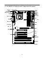


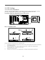
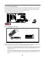
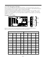

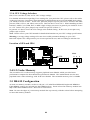
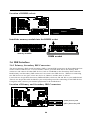
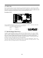
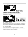
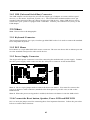

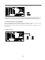


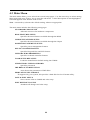


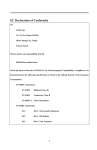
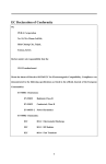


![PDF format [User manual]](http://vs1.manualzilla.com/store/data/005732328_1-c6f560cc59c28b45e6e6b9e007201668-150x150.png)