1
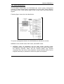
Module A9M2440_0 User's Manual P.O: Box 1103 Kueferstrasse 8 Tel. +49 (7667) 908-0 [email protected] • • • • D-79200 Breisach, Germany D-79206 Breisach, Germany Fax +49 (7667) 908-200 http://www.fsforth.de Module A9M2440_0 Copyright 2005: FS FORTH-SYSTEME GmbH Postfach 1103, D-79200 Breisach a. Rh., Germany Release of Document: Filename: Author: Document Version April 18, 2005 UM_A9M2440.doc Joachim Jaeger 1.0 All rights reserved. No part of this document may be copied or reproduced in any form or by any means without the prior written consent of FS FORTH-SYSTEME GmbH. 2 Module A9M2440_0 1. History Date 2005-04-18 Version 1.0 Responsible J. Jaeger Description First version 3 Module A9M2440_0 Table of Contents 1. History ..............................................................................................................3 2. Introduction.......................................................................................................6 2.1. Benefits of the ModARM9 Concept ........................................................6 2.2. Common Features .................................................................................7 2.3. Variants of A9M2440_0..........................................................................8 2.4. Block Diagram ........................................................................................9 3. Detailed Module Description ..........................................................................10 3.1. Configuration........................................................................................10 3.2. Power ...................................................................................................13 3.3. Clock Generation .................................................................................16 3.4. Reset....................................................................................................20 3.5. JTAG ....................................................................................................21 3.6. SDRAM memory ..................................................................................21 3.7. Flash memory.......................................................................................22 3.8. RTC ......................................................................................................22 3.9. RS232 interface ...................................................................................22 3.10.SPI interface ........................................................................................25 3.11.I2C interface ........................................................................................26 3.12.USB interface.......................................................................................27 3.13.Ethernet interface ................................................................................28 3.14.A/D Converter & Touch Screen Interface ............................................30 3.15.LCD Controller STN LCD, TFT LCD Displays Features ......................31 3.16.Watchdog Timer ..................................................................................32 3.17.IIS-Bus Interface ..................................................................................33 3.18.Camera Interface .................................................................................34 3.19.AC97 Controller ...................................................................................35 3.20.SD Host Interface ................................................................................36 3.21.Clock Output ........................................................................................36 3.22.Power Management.............................................................................37 4. Boot Concept..................................................................................................42 5. Software Requirements ..................................................................................43 5.1. Power Management .............................................................................43 4 Module A9M2440_0 6. Mechanics...................................................................................................... 47 6.1. Extended Module................................................................................. 49 6.2. Nomenclature: ..................................................................................... 50 5 Module A9M2440_0 2. Introduction ARM offers a wide range of 32-bit embedded RISC microprocessors cores based on a common architecture and delivering high performance together with low power consumption and system cost. The ARM processor range provides solutions for: • • • Open platforms running complex operating systems for wireless, consumer and imaging applications. Embedded real-time systems for mass storage, automotive, industrial and networking applications. Secure applications including smart cards and SIMs. There are many manufacturers, who have designed their own CPUs with the ARM9 core, to realize special features. This documentation specifies the MODARM9 module based on the Samsung CPU S3C2410A. 2.1. Benefits of the ModARM9 Concept The concept of the MODARM9 module is, that for some standard functions, common for all modules, always the same pin locations at the system connectors are used. These are called standard pin locations in contrast to the global pin locations. Any other functions, depending on the specific CPU on the module, could have their pins located anywhere at the global pin locations. These locations are defined in the corresponding hardware specification of the module. The aim of the modules is, realizing a high performance at data exchange between CPU and memory, as well as supporting the power management features of each CPU as good as possible, to reduce the power consumption. 6 Module A9M2440_0 2.2. Common Features Below are the common features of the A9M2440 module. • 16/32bit-RISC CPU with ARM920T core with MMU • Size 60mm x 44mm with 240-pin connector • SDRAM 32MB – 128MB • NAND Flash 32MB – 128MB • External RTC, connected to I2C • LCD interface • Touch Screen interface • Camera interface • I²S interface • AC97 Audio-CODEC interface • SD card interface • 3 serial RS232 interfaces • Host and device USB interface, USB1.1 compliant • 10Mbps Ethernet interface • I²C interface, 100KHz and 400KHz • SPI interface • JTAG interface 7 Module A9M2440_0 2.3. Variants of A9M2440_0 Following variants of the A9M2440_0 module are available: 1 V01/0372, 32MB S3C2440@400MHz 8 SDRAM, 32MB NAND Flash, 10Mbit/s Ethernet, Module A9M2440_0 2.4. Block Diagram VLIO RSTIN# Clock Clock Reset Reset Generator Generator Core Core Voltage Voltage PLL PLL Voltage Voltage PWRGOOD RSTOUT# USB host0 JTAG USB PWR Enable Configuration Ethernet-I/F, Ethernet-I/F, PHY PHY COM 0/COM 1 LEDLNK LCD/TFT-I/F LEDH0 Camera-I/F AC97/I2S-I/F S3C2440 S3C2440 Timer Out DMA Ext. INT Analog In Bus Control SPI 120pin Conn 1 SD-I/F Touch Screen Timer In USB host1/device0 Conn 2 PWR Enable Core USB Detect/PWR Enable Battery Fault I2C Serial Serial EEPROM EEPROM 120pin Buffer CLKOUT Buffer RTC RTC VRTC Address Bus VRTC 2 banks 2 banks SDRAM SDRAM Data Bus SDRAM-I/F AVCC +3.3V VLIO Flash Control NAND NAND Flash Flash GND Address Bus AGND GND Data Bus 9 Module A9M2440_0 3. Detailed Module Description Following demands are made by the MODARM9 module concept: • • • CPU configured to little endian 4 pins provided for software configuration, which are routed to the base board at standard pin locations 4 pins provided for hardware configuration, routed to the base board at standard pin locations, where one pin has the meaning of DEBUG ENABLE and one pin has the meaning of NAND Flash write protect. The endianess is configured in register 1 bit 7. This bit has to be 0 for little endian. On reset this bit is set to 0 automatically. Therefore no software configuration is necessary. There are no buffers provided at the module for data- address- and control lines. 3.1. Configuration There are eight configuration pins provided at the system connector four of them are provided as hardware configuration pins, and the other four can be used as software configuration pins. A 10k pullup resistor is provided at each signal line of the configuration pins. The following pins at the connector are defined as hardware configuration pins: 10 Signal Description DEBUGEN# FWP# CONF2 CONF3 Debug Enable Write Protect of internal Flash Hardware Configuration 2 (not used yet) Hardware Configuration 3 (not used yet) Module A9M2440_0 The following port pins are defined as software configuration pins: Signal Port Pin CONF4 CONF5 CONF6 CONF7 The meaning of department. Description GPF2 Software Configuration 0 GPF3 Software Configuration 1 GPF4 Software Configuration 2 GPF5 Software Configuration 3 the configuration pins has to be defined by the software The signal DEBUGEN# (CONF0) from the base board to the module is necessary, to be able to switch on and off a connection between the system reset and the JTAG reset. This will be done with the analog switch MC74VHC1G66: Signal State DEBUGEN# High Description Switch is on, TRST# and PWRGOOD are connected (default) DEBUGEN# Low Switch is off, TRST# and PWRGOOD are disconnected At the module a pull up resistor is provided at the DEBUGEN# signal. Therefore only a jumper to GND is necessary at the base board. Additional configurations can be stored in the serial EEPROM, which will be read by the bootloader at power up (e.g. software version of the module). The CPU specific configuration pins are OM0 – OM3 and NCON. The pins OM0 – OM3 are not routed to the system connector. On the module they are configured as follows: OM1 OM0 0 0 1 1 0 1 0 1 Booting ROM data width Pre-configured Nand Flash Mode 16-bit 32-bit Test Mode Yes No No No 11 Module A9M2440_0 OM[3:2] MPLL UPLL Main CLK Source USB CLK Source Pre-conf. 00 On On Crystal Crystal Yes 01 On On Crystal External Clock No 10 On On External Clock Crystal No 11 On On External Clock External Clock No Although the MPLL starts just after a reset, the MPLL output (Mpll) is not used as the system clock until the software writes valid settings to the MPLLCON register. Before this valid setting, the clock from external crystal or EXTCLK source will be used as the system clock directly. Even if the user wants to maintain the default value of the MPLLCON register, the user should write the same value into the MPLLCON register. There are configuration resistors provided, to give module specific information to the software. These configuration resistors are connected to GPIOs via a multiplexer, so these GPIOs are available again, for common use after initialization of the module. (MCONF3 is connected direct to GPF1, without multiplexer). The signal lines, which are connected to the base board connector, have a 10k pullup resistor each. The multiplexer is switched by GPIO GPH8 (GPIO_ON#). For reading the module specific configuration, this pin has to be at high level, which is also the default state after power up. After the initialization, the software has to switch this port pin to a low level. 12 Module A9M2440_0 Following table shows the Module configuration pins SDRAM-Type SDRAM-CL CPU MCONF0 MCONF1 MCONF2 MCONF3 (GPB0) (GPB1) (GPB2) (GPF1) 1Mx32x4 0 0 x x 2Mx32x4 0 1 x x 4Mx32x4 1 0 x x 2 x x 0 x 3 x x 1 x 400MHz x x x 0 533MHz x x x 1 x = don’t care 3.2. Power The common power supply for the module is 3.3VDC. To use the module also in battery-only supplied devices (mobile devices), an additional power supply pin is provided at the system connector, VLIO. At this pin a one-cell Li-Ion battery can be connected. If no Li-Ion battery is used, or another type of battery within the required voltage range, VLIO has to be connected to 3.3V at the base board. The CPU specific core voltage of 1.2V@300MHz (1.3V@400MHz) and the voltage for VDDalive will be generated on the module from the VLIO input, while the voltage for memory and I/Os is fed direct from the 3.3V. 13 Module A9M2440_0 Following requirements have to be met by the power supply: Power Supply Module Power Supply 3.3V Module Power Supply VLIO Core Voltage @300MHz 3.3V +/- 5% @400MHz 3.3V +/- 5% 2.5V – 4.2V 2.5V – 4.2V (Lithium-Ion (Lithium-Ion battery) battery) 1.2V (1.15V – 1.3V (1.25V – 1.25V) 1.35V) 1.15V – 1.25V 1.15V – 1.35V 3V (1.8V – 3.6V) 3V (1.8V – 3.6V) @533MHz 3.3V +/- 5% 2.5V – 4.2V (Lithium-Ion battery) TBD TBD 3V (1.8V – 3.6V) 3V (e.g. Li3V (e.g. Li3V (e.g. LiBattery) Battery) Battery) 3.3V (3V – 3.6V) 3.3V (3V – 3.6V) 3.3V (3V – 3.6V) -0.3V - 3.3V +/-0.3V - 3.3V +/-0.3V - 3.3V VIN at common CPU 0.3V 0.3V +/- 0.3V pins -0.3V – 5.25V -0.3V – 5.25V VIN, at 5V tolerant CPU -0.3V – 5.25V pins VDDalive Voltage for internal RTC Power Supply for ext. RTC VRTC Analog Voltage The voltage at pin RTCVDD has to be 1.8V, even though the RTC is not used. Therefore this pin is connected to the VDDalive pin on the module. The S3C2440A supports DVS (dynamic voltage scaling). This means, that the core voltage may be reduced to 1V in idle mode, while clock frequency is also reduced. This feature is also supported on the module, by adding a second switching regulator TPS62000, which may dynamically switch between the normal core voltage and 1V. The switching signal (IDLE_SW#) is triggered by software when entering idle mode, by GPG12. (Low = 1V). A further pin VRTC is defined to connect a battery at the base board, for the external RTC on the module. If the external RTC is not used, pin VRTC doesn’t need to be connected, due to a Schottky diode switch-over to 3.3V on the module. VRTC is only used to power the external RTC on the module. 14 Module A9M2440_0 If a battery supplies the power for the module, the pin BATT_FLT# can be connected to a comparator output at the base board. The comparator may supervise the battery voltage at the base board. The CPU does not wake up at power-off mode in case of low battery state. If this feature isn’t used, the pin has to be left open, because a 10k pullup resistor is provided at the module. Analog voltage AVCC and AGND, e.g. for a touch screen, are also provided at the system connector. 15 Module A9M2440_0 3.3. Clock Generation On the module a 16.9344MHz quartz is used to generate the system clock. Therefore the following configuration is needed at Operating Mode pins 2 and 3: OM[3:2] MPLL UPLL Main CLK Source USB CLK Source Pre-conf. 00 On On Crystal Crystal Yes 01 On On Crystal External Clock No 10 On On External Clock Crystal No 11 On On External Clock External Clock No Note: An External Clock is not used, so the pin EXTCLK has to be connected to 3.3V. The MPLL within the clock generator, as a circuit, synchronizes an output signal with a reference input signal in frequency and phase. In this application, it includes the following basic blocks as shown below: the Voltage Controlled Oscillator (VCO) to generate the output frequency proportional to input DC voltage, the divider P to divide the input frequency (Fin) by p, the divider M to divide the VCO output frequency by m which is input to Phase Frequency Detector (PFD), the divider S to divide the VCO output frequency by “s” which is Mpll (the output frequency from MPLL block), the phase difference detector, the charge pump, and the loop filter. The output clock frequency Mpll is related to the reference input clock frequency Fin by the following equation: Mpll = (2*m * Fin) / (p * 2s) m = M (the value for divider M)+ 8, p = P (the value for divider P) + 2 The UPLL within the clock generator is the same as the MPLL in every aspect. Pads for external loop filter capacitors are provided on the module. FCLK is used by ARM920T. HCLK is used for AHB bus, which is used by the ARM920T, the memory controller, the interrupt controller, the LCD controller, the DMA and USB host block. 16 Module A9M2440_0 PCLK is used for APB bus, which is used by the peripherals such as WDT, IIS, I2C, PWM timer, MMC interface, ADC, UART, GPIO, RTC and SPI. The S3C2440A supports selection of Dividing Ratio between FCLK, HLCK and PCLK. This ratio is determined by HDIVN and PDIVN of CLKDIVN control register. The context between FCLK, HCLK and PCLK is shown in the following table: HDIVN PDIVN HCLK3_HALF/ HCLK4_HALF 0 0 – FCLK HCLK PCLK FCLK FCLK FCLK Divide Ratio 1:1:1 0 1 – FCLK FCLK FCLK / 2 1:1:2 1 0 – FCLK FCLK / 2 FCLK / 2 1:2:2 1 1 – FCLK FCLK / 2 FCLK / 4 1:2:4 3 0 0/0 FCLK FCLK / 3 FCLK / 3 1:3:3 3 1 0/0 FCLK FCLK / 3 FCLK / 6 1:3:6 3 0 1/0 FCLK FCLK / 6 FCLK / 6 1:6:6 3 1 1/0 FCLK FCLK / 6 FCLK / 12 1 : 6 : 12 2 0 0/0 FCLK FCLK / 4 FCLK / 4 1:4:4 2 1 0/0 FCLK FCLK / 4 FCLK / 8 1:4:8 2 0 0/1 FCLK FCLK / 8 FCLK / 8 1:8:8 2 1 0/1 FCLK FCLK / 8 FCLK / 16 1 : 8 : 16 Note: Divide Ratio 1:4:8 should be used. After setting PMS value, it is required to set CLKDIVN register. The value set for CLKDIVN will be valid after PLL lock time. The value is also available for reset and changing Power Management Mode. The setting value can also be valid after 1.5 HCLK. Only, 1HCLK can validate the value of CLKDIVN register changed from Default (1:1:1) to other Divide Ratio (1:1:2, 1:2:2, 1:2:4). NOTES 1. CLKDIVN should be set carefully not to exceed the limit of HCLK and PCLK. 17 Module A9M2440_0 2. If HDIVN is not 0, the CPU bus mode has to be changed from the fast bus mode to the asynchronous bus mode using following instructions (S3C2440A does not support synchronous bus mode): MMU_SetAsyncBusMode mrc p15,0,r0,c1,c0,0 orr r0,r0,#R1_nF:OR:R1_iA mcr p15,0,r0,c1,c0,0 If HDIVN is not 0 and the CPU bus mode is the fast bus mode, the CPU will operate by the HCLK. This feature can be used to change the CPU frequency as a half or more without affecting the HCLK and PCLK. 18 Module A9M2440_0 Following table shows the recommended values for FCLK: Input Frequency (Fin , MHz) Output Frequency (FCLK, MHz) MDIV PDIV SDIV 12.0000MHz 48.00 MHz (Note) 56(0x38) 2 2 12.0000MHz 96.00 MHz (Note) 56(0x38) 2 1 12.0000MHz 271.50 MHz 173(0xad) 2 2 12.0000MHz 304.00 MHz 68(0x44) 1 1 12.0000MHz 405.00 MHz 127(0x7f) 2 1 12.0000MHz 532.00 MHz 125(0x7d) 1 1 16.9344MHz 47.98 MHz (Note) 60(0x3c) 4 2 16.9344MHz 95.96 MHz (Note) 60(0x3c) 4 1 16.9344MHz 266.72 MHz 118(0x76) 2 2 16.9344MHz 296.35 MHz 97(0x61) 1 2 16.9344MHz 399.65 MHz 110(0x6e) 3 1 16.9344MHz 530.61 MHz 86(0x56) 1 1 16.9344MHz 533.43 MHz 118(0x76) 1 1 NOTE: The 48.00MHz and 96MHz output is used for UPLLCON register. The 48.00MHz/47.98MHz output is used for USB, and the corresponding values have to be written into UPLLCON register. The 405.00MHz/399.65MHz output is used as FCLK and the corresponding values have to be written into PLLCON register. 19 Module A9M2440_0 NOTE: When you set MPLL&UPLL values, you have to set the UPLL value first and then the MPLL value. (Needs intervals approximately 7 NOP) These are the resulting Clock values: Quartz FCLK HCLK PCLK 101.25 MHz 50.625 MHz 12.0000 MHz 405.00 MHz 49.956 MHz 16.9344 MHz 399.65 MHz 99.9125 MHz Note: 16.9344MHz is used to meet better Audio frequencies UCLK 48.00 MHz 47.98 MHz The Clock control logic in S3C2440A can generate the required clock signals including FCLK for CPU, HCLK for the AHB bus peripherals, and PCLK for the APB bus peripherals. The S3C2440A has two Phase Locked Loops (PLLs): one for FCLK, HCLK, and PCLK, and the other dedicated for USB block (48Mhz). The clock control logic can make slow clocks without PLL and connect/disconnect the clock to each peripheral block by software, which will reduce the power consumption. 3.4. Reset There are 3 reset signals defined, which are routed to the system connector: • • • a reset input to the module (RSTIN#) an output of the reset controller from the module (PWRGOOD) a reset output from the CPU (RSTOUT#) The low active Reset input at the CPU suspends any operation in progress and places S3C2440A into a known reset state. PWRGOOD (system reset signal) must be held to low level at least 4 CLKs to recognize the reset signal and it takes 128 CLKs between PWRGOOD and internal RESET#. TPS3307 from Texas Instruments is used as reset generator. It supervises the incoming 3.3V with the Sense1 input, while the Sense2 and Sense3 inputs are not used. The MR#-input is used to supervise the RSTIN# signal. TPS3307 has push-pull low and high active reset outputs, with a threshold voltage of 2.93V. 20 Module A9M2440_0 The reset pulse width is 200ms min. The low active reset output is connected to the system reset via a 470R series resistor. The high active reset output is used for the ethernet controller. RSTIN# signal from the base board is connected to the reset generator device on the module. At the base board there could be a reset switch connected to the RSTIN# signal. A 10k pullup resistor is connected to the RSTIN# signal on the module. RSTOUT# can be used for external device reset control. RSTOUT# is a function of Watchdog Reset and Software Reset (RSTOUT# = PWRGOOD & WDTRST# & SW_RESET). 3.5. JTAG The standard JTAG signals are provided at the system connector. A JTAG/MultiICE connector has to be provided at the base board for debugging and bootloader purposes. The signal DEBUGEN# (CONF0) from the base board to the module is necessary, to be able to switch on and off a connection between the system reset and the JTAG reset. The pull-up resistors, belonging to the JTAG interface, are placed on the module. 3.6. SDRAM memory On the module there are two banks provided for SDRAM memory. Bank 1 provides one part of a 32bit SDRAM in a 90 ball-FBGA package, with 3.3V power supply, while bank 2 is only populated for 128MByte SDRAM (2 x 64MByte). Total size of memory is possible from 16MB (only one bank) up to 128MB (64MB each bank). Both banks have to be populated with equal devices. 21 Module A9M2440_0 3.7. Flash memory NAND Flash memory is provided, as a single Flash device. Bus size of the Flash device is 8bit, in a 48pin TSOP package, with 3.3V power supply. The Flash memory contains the bootloader and the application software. The page size of these devices has to be 512bytes. Total size of memory is possible from 32MB up to 128MB. 3.8. RTC The internal RTC is not used. Instead of the internal RTC an external one is used. This RTC is connected to the I2C bus and powered by a 3V battery, which has to be mounted at the base board. If no RTC is used, the pin VRTC at the system connector can be left floating, because two Schottky diodes are used to power the RTC either from 3.3V, or from the battery. The state of this battery will not be supervised on the module. The external RTC is the DS1337 from Dallas. It is a CMOS real time clock/calendar optimized for low power consumption. An interrupt output is provided. All address and data are transferred serially via a two-line bidirectional I2C-bus. Maximum bus speed is 400 kbit/s. The low active interrupt output (CLK_INT#) of the RTC is connected to interrupt input EINT7 of the CPU. The I2C device address of the RTC is D0H. 3.9. RS232 interface At the system connector, there are the signals for two RS232 interfaces provided. Each interface consists of the data lines RXD/TXD and the handshake lines RTS#/CTS#. The UARTS are part of the CPU. If the handshake lines of the second RS232 interface (RTS1#/CTS1#) are not used, they could be used as data lines for a third RS232 interface (TXD2/RXD2). 22 Module A9M2440_0 The S3C2440A Universal Asynchronous Receiver and Transmitter (UART) provide three independent asynchronous serial I/O (SIO) ports, each of which can operate in Interrupt-based or DMA-based mode. In other words, the UART can generate an interrupt or a DMA request to transfer data between CPU and the UART. The UART can support bit rates up to 115.2K bps using system clock. If an external device provides the UART with UEXTCLK, then the UART can operate at higher speed. Each UART channel contains two 64-byte FIFOs for receiver and transmitter. The S3C2440A UART includes programmable baud rates, infrared (IR) transmit/receive, one or two stop bit insertion, 5-bit, 6-bit, 7-bit or 8-bit data width and parity checking. Each UART contains a baud-rate generator, transmitter, receiver and a control unit. The baud-rate generator can be clocked by PCLK, FCLK/n or UEXTCLK (external input clock). The transmitter and the receiver contain 64-byte FIFOs and data shifters. Data is written to FIFO and then copied to the transmit shifter before being transmitted. The data is then shifted out by the transmit data pin (TxDn). Meanwhile, received data is shifted from the receive data pin (RxDn), and then copied to FIFO from the shifter. The S3C2440A UART block supports also infra-red (IR) transmission and reception, which can be selected by setting the Infra-red-mode bit in the UART line control register (ULCONn). Figure below illustrates how to implement the IR mode. In IR transmit mode, the transmit pulse comes out at a rate of 3/16, the normal serial transmit rate (when the transmit data bit is zero); In IR receive mode, the receiver must detect the 3/16 pulsed period to recognize a zero value. 23 Module A9M2440_0 Baud-Rate Generation: Each UART's baud-rate generator provides the serial clock for the transmitter and the receiver. The source clock for the baud-rate generator can be selected with the S3C2440A's internal system clock or UEXTCLK. In other words, dividend is selectable by setting Clock Selection of UCONn. The baud-rate clock is generated by dividing the source clock (PCLK, FCLK/n or UEXTCLK) by 16 and a 16-bit divisor specified in the UART baud-rate divisor register (UBRDIVn). The UBRDIVn can be determined by the following expression: UBRDIVn = (int)( UART clock / ( baud rate x 16) ) –1 where, the divisor should be from 1 to (216-1). UART baud-rate generator error tolerance: UART Frame error should be less than 1.87%(3/160). tUPCLK = (UBRDIVn + 1) x 16 x 1Frame / PCLK Clock tUPCLK: tUEXACT = 1Frame / baud-rate Clock tUEXACT: UART error = (tUPCLK – tUEXACT) / tUEXACT x 100% 24 Real Ideal UART UART Module A9M2440_0 Following table shows the baudrate with the corresponding value for UBRDIV: PCLK (MHz) 50.7 50.7 50.7 50.7 Baudrate 9600 19200 38400 115200 UBRDIV 329 164 81 26 Error (%) -0.02366864 -0.02366864 -0.6295858 -1.84142012 3.10. SPI interface The S3C2440A includes two SPI-interfaces, each of it has two 8-bit shift registers for transmission and receiving, respectively. During an SPI transfer, data is simultaneously transmitted (shifted out serially) and received (shifted in serially). 8-bit serial data at a frequency is determined by its corresponding control register settings. If you only want to transmit, received data can be dummy. Otherwise, if you only want to receive, you should transmit dummy '1' data. There are 4 I/O pin signals associated with SPI transfers: the SCK (SPICLK0,1), the MISO (SPIMISO0,1) data line, the MOSI (SPIMOSI0,1) data line, and the active low /SS (nSS0,1) pin (input). Both 4-pin-SPI-interfaces are provided at the system connector (Clock, ChipSelect, Data-In and Data-Out). SPI0 interface is located at the general pins of the system connector, while SPI1 interface shares it’s pins with interrupt functions at the specific pins of the system connector. Features: • • • • • SPI Protocol (ver. 2.11) compatible 8-bit Shift Register for transmit 8-bit Shift Register for receive 8-bit Prescaler logic Polling, Interrupt, and DMA transfer mode 25 Module A9M2440_0 3.11. I2C interface The I2C signals clock and data are provided at the system connector. On the module there is a serial EEPROM connected to the I2C interface and the external RTC. As the EEPROM and the RTC are supplied by 3.3V, the I2C components, which should be connected to I2C interface at the base board, have to be supplied also by 3.3V or level shifters are needed. Problem: The tSDAH (SDA data hold time) is min. 0ns by the specification. But, the real tSDAH is 3-clock duration based on MCLK or PCLK. This tSDAH may be insufficient for some IIC slave device. A few slave devices may not receive the valid address sometimes due to the lack of SDA hold time and will not acknowledge in spite of a valid addressing. If the SDA data hold time is insufficient, the error occurs very rarely and at random time. Workaround: If any device needs more SDA data hold time than 3 MCLK (or PCLK), RC delay circuit is needed on the SDA line as follows: For example, R=100R and C=200pF can be one of available values. We recommend implementing the RC delay circuit on SDA line for case of need. Mostly it may not be needed. On the module a 0R resistor is fitted and the capacitor is not equipped on the SDA line to the RTC and the EEPROM. If needed, the workaround mentioned above, could be realized. 26 Module A9M2440_0 3.12. USB interface The S3C2440A provides two USB ports. One of it can only be used as host interface, the other port can be configured either as host or device interface. S3C2440A supports 2-port USB host interfaces as follows: • • • • OHCI Rev 1.0 compatible USB Rev1.1 compatible Two down stream ports Support for both LowSpeed and HighSpeed USB devices The USB device controller is designed to provide a high performance full speed function controller solution with DMA interface. USB device controller allows bulk transfer with DMA, interrupt transfer and control transfer. The 22R series resistors for both ports have to be mounted at the base board. USB device controller supports: • • • • Full speed USB device controller compatible with the USB specification version 1.1 DMA interface for bulk transfer Five endpoints with FIFO Integrated USB Transceiver Feature: • • • • • • • • Fully compliant with USB Specification Version 1.1 Full speed (12Mbps) device Integrated USB Transceiver Supports control, interrupt and bulk transfer Five endpoints with FIFO: Supports DMA interface for receive and transmit bulk endpoints. (EP1, EP2, EP3, and EP4) Independent 64byte receive and transmit FIFO to maximize throughput Supports suspend and remote wakeup function 27 Module A9M2440_0 One USB interface is provided at the general pins of the system connector, consisting of the data lines USBP and USBN as well as the additional signal USB_DT/PW. Depending on the base board, the USB interface can be realised either as host1 or device0, the signals have the following meaning: Signal USB host1 USB device0 USBP Differential data+ DP1 Differential data+ PDP0 USBN Differential data- DN1 Differential data- PDN0 USB_DT/PW USB Power Enable USB Detect At the module specific pins of the system connector a second host interface (host0) is provided with the differential data lines DP0 and DN0. 3.13. Ethernet interface The A9M2440 module has an external 10Mbit Ethernet controller with integrated MAC and PHY on board. The CS8900A from Cirrus Logic will be used as single chip IEEE 802.3 Ethernet Controller. It operates at 3.3V and uses a 20MHz quartz crystal. DMA mode is not supported. Feature: • Full Duplex Operation • On-Chip RAM buffers transmit and receive frames • 10Base-T port with analog filters provides automatic polarity detection and correction • Programmable Transmit features Automatic retransmission on collision Automatic padding and CRC generation 28 Module A9M2440_0 • Programmable Receive features Stream transfer for reduced CPU overhead Auto switch between DMA and On-Chip memory Early interrupts for Frame preprocessing Automatic rejection for Erroneous packets • LED drivers for Link status and LAN activity • Standby and Suspend Sleep modes The CS8900A is accessed by the control lines CS5#, OE# and WE# modified by address line A24, to generate IO- and memory accesses. Its high active interrupt output is connected to the interrupt input EINT9 of the CPU. The serial EEPROM, connected to the I2C-bus of the CPU will be used as storage for the MAC-address. At the global signals at the system connector only the signal for the Link/ActivityLED is used. The CS8900A provides both LED-signals, therefore Link and Activity are combined to one signal LEDLNK#. The signal for the 10/100Mbit LED is not connected. At the base board it is necessary to use a transformer with 1:2.5 turns ratio on TX and 1:1 on RX, like the Halo TG41-2006N. Following table shows the configuration for the BANKCON5 register: BANKCON5 MT Tacs Tcos Tacc Tcoh Tcah Tacp PMC CS8900 00 00 11 111 01 00 11 00 Remark 29 Module A9M2440_0 3.14. A/D Converter & Touch Screen Interface The 10-bit CMOS ADC (Analog to Digital Converter) is a recycling type device with 8-channel analog inputs. It converts the analog input signal into 10-bit binary digital codes at a maximum conversion rate of 500KSPS with 2.5MHz A/D converter clock. A/D converter operates with on-chip sample-and-hold function and power down mode is supported. Touch Screen Interface can control/select pads (XP, XM, YP, YM) of the Touch Screen for X, Y position conversion. Touch Screen Interface contains Touch Screen Pads control logic and ADC interface logic with an interrupt generation logic. Feature: • • • • • • • • • • • • 30 Resolution: 10-bit Differential Linearity Error: ± 1.0 LSB Integral Linearity Error: ± 2.0 LSB Maximum Conversion Rate: 500 KSPS Low Power Consumption Power Supply Voltage: 3.3V Analog Input Range: 0 ~ 3.3V On-chip Sample-and-hold Function Normal Conversion Mode Separate X/Y position conversion Mode Auto (Sequential) X/Y Position Conversion Mode Waiting for Interrupt Mode Module A9M2440_0 3.15. LCD Controller STN LCD, TFT LCD Displays Features The LCD controller in the S3C2440A consists of the logic for transferring LCD image data from a video buffer located in system memory to an external LCD driver. The LCD controller supports monochrome, 2-bit per pixel (4-level gray scale) or 4-bit per pixel (16-level gray scale) mode on a monochrome LCD, using a time-based dithering algorithm and Frame Rate Control (FRC) method and it can be interfaced with a color LCD panel at 8-bit per pixel (256-level color) and 12-bit per pixel (4096-level color) for interfacing with STN LCD. It can support 1-bit per pixel, 2-bit per pixel, 4-bit per pixel, and 8-bit per pixel for interfacing with the palletized TFT color LCD panel, and 16-bit per pixel and 24bit per pixel for non-palletized true-color display. The LCD controller can be programmed to support different requirements on the screen related to the number of horizontal and vertical pixels, data line width for the data interface, interface timing, and refresh rate. Features: STN LCD Displays: • Supports 3 types of LCD panels: 4-bit dual scan, 4-bit single scan, and 8-bit single scan display type • Supports the monochrome, 4 gray levels, and 16 gray levels • Supports 256 colors and 4096 colors for color STN LCD panel • Supports multiple screen size: Typical actual screen size: 640 x 480, 320 x 240, 160 x 160, and others Maximum virtual screen size is 4Mbytes. Maximum virtual screen size in 256 color mode: 4096 x 1024, 2048 x 2048, 1024 x 4096, and others TFT LCD Displays: 31 Module A9M2440_0 • Supports 1, 2, 4 or 8-bpp (bit per pixel) palletized color displays for TFT • Supports 16, 24-bpp non-palletized true-color displays for color TFT • Supports maximum 16M color TFT at 24bit per pixel mode • Supports multiple screen size Typical actual screen size: 640 x 480, 320 x 240, 160 x 160, and others Maximum virtual screen size is 4Mbytes. Maximum virtual screen size in 64K color mode: 2048 x 1024 and others 3.16. Watchdog Timer The S3C2440A watchdog timer is used to resume the controller operation whenever it is disturbed by malfunctions such as noise and system errors. It can be used as a normal 16-bit interval timer to request interrupt service. The watchdog timer generates the reset signal for 128 PCLK cycles. Feature: • 16-bit Watchdog Timer • Interrupt request or system reset at time-out The prescaler value and the frequency division factor are specified in the watchdog timer control (WTCON) register. Valid prescaler values range from 0 to 28-1. The frequency division factor can be selected as 16, 32, 64, or 128. Use the following equation to calculate the watchdog timer clock frequency and the duration of each timer clock cycle: t_watchdog = 1/( PCLK / (Prescaler value + 1) / Division_factor ) with PCLK = 50.70 MHz. 32 Module A9M2440_0 3.17. IIS-Bus Interface Currently, many digital audio systems are attracting the consumers on the market, in the form of compact discs, digital audio tapes, digital sound processors, and digital TV sound. The S3C2440A Inter-IC Sound (IIS) bus interface can be used to implement a CODEC interface to an external 8/16-bit stereo audio CODEC IC for minidisc and portable applications. The IIS bus interface supports both IIS bus data format and MSB-justified data format. The interface provides DMA transfer mode for FIFO access instead of an interrupt. It can transmit and receive data simultaneously as well as transmit or receive data alternatively at a time. Feature: • 1-ch IIS-bus for audio interface with DMA-based operation • Serial, 8-/16-bit per channel data transfers • 128 Bytes (64-Byte + 64-Byte) FIFO for Tx/Rx • Supports IIS format and MSB-justified data format Functional Description: Bus interface, register bank, and state machine (BRFC): Bus interface logic and FIFO access are controlled by the state machine. • 5-bit dual prescaler (IPSR): One prescaler is used as the master clock generator of the IIS bus interface and the other is used as the external CODEC clock generator. • 64-byte FIFOs (TxFIFO and RxFIFO): In transmit data transfer, data are written to TxFIFO, and, in the receive data transfer, data are read from RxFIFO. • Master IISCLK generator (SCLKG): In master mode, serial bit clock is generated from the master clock. • Channel generator and state machine (CHNC): IISCLK and IISLRCK are generated and controlled by the channel state machine. 33 Module A9M2440_0 • 16-bit shift register (SFTR): Parallel data is shifted to serial data output in the transmit mode, and serial data input is shifted to parallel data in the receive mode. 3.18. Camera Interface This chapter will explain the specification and defines the camera interface. CAMIF (CAMera InterFace) within the S3C2440A consists of 7 parts – pattern mux, capturing unit, preview scaler, codec scaler, preview DMA, codec DMA, and SFR. The CAMIF supports ITU-R BT.601/656 YCbCr 8-bit standard. Maximum input size is 4096x4096 pixels (2048x2048 pixels for scaling) and two scalers exist. Preview scaler is dedicated to generate smaller size image like PIP (Picture In Picture) and codec scaler is dedicated to generate codec useful image like plane type YCbCr 4:2:0 or 4:2:2. Two master DMAs can do mirror and rotate the captured image for mobile environments. These features are very useful in folder type cellular phones and the test pattern generated can be useful in calibration of input sync signals as CAMHREF, CAMVSYNC. Also, video sync signals and pixel clock polarity can be inverted in the CAMIF side by using register setting. Feature: • ITU-R BT. 601/656 8-bit mode support • DZI (Digital Zoom In) capability • Programmable polarity of video sync signals • Max. 4096 x 4096 pixels input support (2048 x 2048 pixel input support for scaling) • Image mirror and rotation (X-axis mirror, Y-axis mirror, and 180° rotation) • PIP and codec input image generation (RGB 16/24-bit format and YCbCr 4:2:0/4:2:2 format) External Interface: CAMIF can support the next video standards. 34 Module A9M2440_0 • ITU-R BT 601 YCbCr 8-bit mode • ITU-R BT 656 YCbCr 8-bit mode Caution! All external camera interface IOs are recommended to be Schmitttrigger type IO for noise reduction. 3.19. AC97 Controller The AC97 Controller Unit of the S3C2440A supports AC97 revision 2.0 features. AC97 Controller communicates with AC97 Codec using an audio controller link (AC-link). Controller sends the stereo PCM data to Codec. The external digitalto-analog converter (DAC) in the Codec then converts the audio sample to an analog audio waveform. Also, the Controller receives the stereo PCM data and the mono Mic data from the Codec and then stores them in the memories. This chapter describes the programming model for the AC97 Controller Unit. The information in this chapter requires an understanding of the AC97 revision 2.0 specifications. Note: The AC97 Controller and the IIS Controller must not be used at the same time. Feature: • Independent channels for stereo PCM In, stereo PCM Out, mono MIC In. • DMA-based operation and interrupt based operation. • All of the channels support only 16-bit samples. • Variable sampling rate AC97 Codec interface (48 KHz and below) • 16-bit, 16 entry FIFOs per channel • Only Primary CODEC support 35 Module A9M2440_0 3.20. SD Host Interface The S3C2440A Secure Digital Interface (SDI) can interface for SD memory card, SDIO device and Multi-Media Card (MMC). Feature: • SD Memory Card Spec. (ver. 1.0) / MMC Spec. (2.11) compatible • SDIO Card Spec (ver. 1.0) compatible • 16 words (64 bytes) FIFO (depth 16) for data Tx/Rx • 40-bit Command Register • 136-bit Response Register • 8-bit Prescaler logic (Freq. = System Clock / (P + 1)) • Normal, and DMA Data Transfer Mode (byte, halfword, word transfer) • 1bit / 4bit (wide bus) Mode & Block / Stream Mode Switch support • DMA burst4 access support(only word transfer) 3.21. Clock Output At the global pins of the system connector there is a clock signal available (BCLKOUT0), which is buffered by a clock buffer and can be choosen to be either MPLL CLK, UPLL CLK, FCLK, HCLK, PCLK or DCLK. The source of this clock signal is the CLKOUT0 port at the CPU, which can be programmed to different clocks, by the CLKSEL0 register. Following table shows the bits [6:4] of the CLKSEL0 register: CLKSEL0 000 [6:4] 001 010 CLKOUT0 MPLL CLK UPLL CLK FCLK HCLK 36 011 100 101 11x PCLK DCLK0 Reserved Module A9M2440_0 3.22. Power Management For the power control logic, the S3C2440A has various power management schemes to keep optimal power consumption for a given task. These schemes are related to PLL, clock control logics (FCLK, HCLK, and PCLK) and wakeup signals. Following figure shows the clock distribution: The power management block in the S3C2440A can activate four modes: NORMAL mode, SLOW mode, IDLE mode, and SLEEP mode. • NORMAL mode: all peripherals and the basic blocks including power management block, the CPU core, the bus controller, the memory controller, the interrupt controller, DMA, and the external master may operate completely. But, the clock to each peripheral, except the basic blocks, can be stopped selectively by software to reduce the power consumption. 37 Module A9M2440_0 • SLOW mode: Power consumption can be reduced in the SLOW mode by applying a slow clock and excluding the power consumption from the PLL. The FCLK is the frequency of divide_by_n of the input clock (XTIpll or EXTCLK) without PLL. The divider ratio is determined by SLOW_VAL in the CLKSLOW control register and CLKDIVN control register. In SLOW mode, PLL will be turned off to reduce the PLL power consumption. When the PLL is turned off in the SLOW mode and the user changes power mode from SLOW mode to NORMAL mode, then the PLL needs clock stabilization time (PLL lock time). This PLL stabilization time is automatically inserted by the internal logic with lock time count register. The PLL stability time will take 300us after the PLL is turned on. During PLL lock time, the FCLK becomes SLOW clock. Users can change the frequency by enabling SLOW mode bit in CLKSLOW register in PLL on state. The SLOW clock is generated during the SLOW mode. • 38 IDLE mode: In IDLE mode, the clock to the CPU core is stopped except the bus controller, the memory controller, the interrupt controller, and the power management block. To exit the IDLE mode, EINT[23:0], or RTC alarm Module A9M2440_0 interrupt, or the other interrupts should be activated. (EINT is not available until GPIO block is turned on). • SLEEP mode: The block disconnects the internal power. So, there occurs no power consumption due to CPU and the internal logic except the wake-up logic in this mode. Activating the SLEEP mode requires two independent power sources. One of the two power sources supplies the power for the wake-up logic. The other one supplies other internal logics including CPU, and should be controlled for power on/off. In the SLEEP mode, the second power supply source for the CPU and internal logics will be turned off. The wakeup from SLEEP mode can be issued by the EINT[15:0]. In SLEEP mode, VDDi, VDDiarm, VDDMPLL and VDDUPLL will be turned off, which is controlled by PWREN pin. If PWREN signal is activated(H), VDDi and VDDiarm are supplied by an external voltage regulator. If PWREN pin is inactive (L), the VDDi and VDDiarm are turned off. In Power_OFF mode the VDDalive pin has still to be supplied by 1.2V/1.3V and it is also necessary to provide the I/O-voltage of 3.3V. Therefore the LDO, which supplies VDDAlive will not be switched off. 39 Module A9M2440_0 The pin state in SLEEP mode should be as follows: NOTE: 1. ADC should be set to Standby mode. 2. USB pads should be Suspend mode. Following figure shows the Power Management State Diagram: RTC alarm could not be used, because instead of the internal RTC, an external one is used. 40 Module A9M2440_0 Following table shows the Clock and Power State in Each Power Mode: Mode ARM920T Normal O AHB Modules/WDT (1) O Power Management GPIO O SEL APB Modules & USBH/LCD/NAN D(2) SEL Idle X O O SEL SEL Slow O O O SEL SEL Sleep OFF OFF Wait for wakeup event Previous state OFF NOTES: (1) USB host, LCD, and NAND are excluded. (2) WDT is excluded. RTC interface for CPU access is included. (3) SEL: selectable (O,X), O: enable, X: disable, OFF: power is turned off A Battery Fault Signal (BATT_FLT#) is provided at the CPU to recognize the battery state of the battery at the base board, which powers the module. Therefore this pin is routed to the system connector. At the base board a comparator has to supervise the battery state and the output of the comparator delivers the BATT_FLT# signal. There are two functions in BATT_FLT# pin as follows: • When CPU is not in SLEEP mode, BATT_FLT# pin will cause the interrupt request by setting BATT_FUNC(MISCCR[22:20]) as 10x’b. The interrupt attribute of the BATT_FLT# is L-level triggered. • While CPU is in SLEEP mode, assertion of the BATT_FLT# will prohibit the wake up from the sleep mode, which is achieved by setting BATT_FUNC(MISCCR[22:20]) as 11x’b. So, Any wake-up source will be masked if BATT_FLT# is asserted, which is protecting the system malfunction of the low battery capacity. 41 Module A9M2440_0 4. Boot Concept The procedure of booting the module is as follows: After power up, an inital programm loader is started by the CPU. This software calls the actual bootloader, which is common for Linux and WinCE. By the bootloader the software image of the customer can be downloaded into the target. S3C2440A boot code will be executed from internal NAND flash memory. In order to support NAND flash bootloader, the S3C2440A is equipped with an internal SRAM buffer called ‘Steppingstone’. When booting, the first 4KBytes of the NAND flash memory will be loaded into Steppingstone and the boot code loaded into Steppingstone will be executed. Generally, the boot code will copy NAND flash content to SDRAM. Using hardware ECC, the NAND flash data validity will be checked. Upon the completion of the copy, the main program will be executed on the SDRAM. 42 Module A9M2440_0 5. Software Requirements 5.1. Power Management Procedure to Enter SLEEP mode • Set the GPIO configuration adequate for SLEEP mode. • Mask all interrupts in the INTMSK register. • Configure the wake-up sources properly including RTC alarm (RTC alarm cannot be used). The bit of EINTMASK corresponding to the wake-up source has not to be masked in order to let the corresponding bit of SRCPND or EINTPEND set. Although a wake-up source is issued and the corresponding bit of EINTMASK is masked, the wake-up will occur and the corresponding bit of SRCPND or EINTPEND will not be set. • Set USB pads as suspend mode. (MISCCR[13:12]=11b) • Save some meaning values into GSTATUS3,4 register. These registers are preserved during SLEEP mode. • Configure MISCCR[1:0] for the pull-up resisters on the data bus,D[31:0]. Turn on the pull-up resistors. • Stop LCD by clearing LCDCON1.ENVID bit. • Read rREFRESH and rCLKCON registers in order to fill the TLB. • Let SDRAM enter the self-refresh mode by setting the REFRESH[22]=1b. • Wait until SDRAM self-refresh is effective. • Set MISCCR[19:17]=111b to make SDRAM signals(SCLK0,SCLK1 and SCKE) protected during SLEEP mode • Set the SLEEP mode bit in the CLKCON register. 43 Module A9M2440_0 Note: The ADC has an additional power-down bit in ADCCON. If the S3C2440A enters the SLEEP mode, the ADC should enter its own power-down mode. Procedure to Wake-up from SLEEP mode • The internal reset signal will be asserted if one of the wake-up sources is issued. This reset duration is determined by the internal 16-bit counter logic and the reset assertion time is calculated as tRST = (65535 /XTAL_frequency). • Check GSTATUS2[2] in order to know whether or not the power-up is caused by the wake-up from SLEEP mode. • Release the SDRAM signal protection by setting MISCCR[19:17]=000b. • Configure the SDRAM memory controller. • Wait until the SDRAM self-refresh is released. Mostly SDRAM needs the refresh cycle of all SDRAM row. • The information in GSTATUS3,4 can be used for user’s own purpose because the value in GSTATUS3,4 has been preserved during SLEEP mode. • For EINT[3:0], check the SRCPND register. • For EINT[15:4], check the EINTPEND instead of SRCPND (SRCPND will not be set although some bits of EINTPEND are set.). • If there was the BATT_FLT# assertion during SLEEP mode, the corresponding bit of SRCPND has been set. Signaling EINT[15:0] for Wakeup The S3C2440A can be woken up from SLEEP mode only if the following conditions are met: • 44 Level signals (H or L) or edge signals (rising or falling or both) are asserted on EINTn input pin. Module A9M2440_0 • The EINTn pin has to be configured as EINT in the GPIO control register. • BATT_FLT# pin has to be H level. It is important to configure the EINTn in the GPIO control register as an external interrupt pin, considering the first condition above. Just after the wake-up, the corresponding EINTn pin will not be used for wakeup. This means that the pin can be used as an external interrupt request pin again. There are two functions in BATT_FLT# pin, they are as follows; • When CPU is not in SLEEP mode, nBATT_FLT pin will cause the interrupt request by setting BATT_FUNC(MISCCR[22:20]) as 10x’b. The interrupt attribute of the BATT_FLT# is L-level triggered. • While CPU is in SLEEP mode, assertion of the BATT_FLT# will prohibit the wake up from the sleep mode, which is achieved by setting BATT_FUNC(MISCCR[22:20]) as 11x’b. So, Any wake-up source will be masked if BATT_FLT# is asserted, which is protecting the system malfunction of the low battery capacity Entering IDLE Mode If CLKCON[2] is set to 1 to enter the IDLE mode, the S3C2440A will enter IDLE mode after some delay (until the power control logic receives ACK signal from the CPU wrapper). PLL On/Off The PLL can only be turned off for low power consumption in slow mode. If the PLL is turned off in any other mode, MCU operation is not guaranteed. When the processor is in SLOW mode and tries to change its state into other state with the PLL turned on, then SLOW_BIT should be clear to move to another state after PLL stabilization Pull-up Resistors on the Data Bus and SLEEP Mode 45 Module A9M2440_0 In SLEEP mode, the data bus (D[31:0] or D[15:0] ) is in Hi-z state. But, because of the characteristics of I/O pad, the data bus pull-up resistors have to be turned on for low power consumption in SLEEP mode. D[31:0] pin pull-up resistors can be controlled by the GPIO control register (MISCCR). 46 Module A9M2440_0 6. Mechanics The module size is defined to 60 x 44mm. Two holes, for M2 screws, catercornered, are provided to enable fixing of the module at the base board. Two board to board connectors are used on the module. Depending on the counterpart at the base board, different distances between module and base board can be realized. The least possible distance is 5mm. Therefore the height of the parts mounted at the bottom side of the module should not exceed 2.5mm. The height of the parts mounted at the top side should not exceed 4.1mm so that the module can fit on a carrier board which is rack-mounted, assumes that the maximum height allowed from top of base board is 13.7mm (8+1.6+4.1). Board-to-Board Module Connector X1, X2 Distance h No. of Pins Qty Supplier Order No. 5 mm 6 mm 7 mm 8 mm 120 2 AMP Berg 177983-5 61082-121000 Base Board Connector X1, X2 No. Of Pins Supplier Order No. 120 AMP 177984-5 Berg 61083-121000 120 AMP 179029-5 Berg 61083-122000 120 AMP 179030-5 Berg 61083-123000 120 AMP 179031-5 Berg 61083-124000 47 Module A9M2440_0 Mechanical Drawing from TOP View: 1 34 39.8 44 X1 Ø 2.2 (2x) 4.2 X2 10 1 2.4 3.9 56.1 57.6 60 h 2.5 4.1 Mechanical Drawing from Side View: 28.4 The size of h depends on the board to board connectors. The size between the board to board connectors is measured from pad to pad. 48 Module A9M2440_0 6.1. Extended Module For further modules it might be necessary to have some additional hardware placed on the module, which will need more signal lines connected between module and base board, than actual available. To meet these future requirements, an extended board is defined, which has two additional board to board connectors with 60 pins each. The size of the extended module is defined to 92 x 44mm. Two holes, for M2 screws, catercornered, are provided to enable fixing of the module at the base board. Board-to-Board Module Connector X3, X4 Distance h No. of Pins Qty Supplier Order No. 5 mm 6 mm 7 mm 8 mm 60 2 AMP Berg 177983-2 61082-061009 Base Board Connector X3, X4 No. Of Pins Supplier Order No. 60 AMP 177984-2 Berg 61083-061009 60 AMP 179029-2 Berg 61083-062009 60 AMP 179030-2 Berg 61083-063009 60 AMP 179031-2 Berg 61083-064009 49 Module A9M2440_0 Mechanical Drawing from TOP View: 1 1 X3 34 Ø 2.2 (2x) 1 1 4.2 X2 X4 10 44 39.8 X1 2.4 3.9 56.1 60.8 89 89.6 92 6.2. Nomenclature: Pin 1 of X1 and X3 is always at the outer row of the connector and pin 1 of X2 and X4 is always at the inner row of the connector. The reference names X1, X2, X3 and X4 are reserved names for the connectors at the MODARM9 modules and their corresponding base boards. These names shouldn’t be used for other connectors. 50