1
EE-379 Embedded Systems and Applications
Intro to ARM Cortex-M3 (CM3) and LPC17xx MCU
Cristinel Ababei
Department of Electrical Engineering, University at Buffalo
Spring 2013
Note: This course is offered as EE 459/500 in Spring 2013
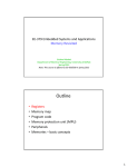
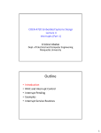
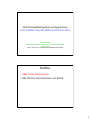
Outline
• ARM Cortex-M3 processor
• NXP LPC17xx microcontroller unit (MCU)
1
Cortex-M3 Processor
• RISC general purpose 32-bit microprocessor, released
2006
• Cortex-M3 differs from previous generations of ARM
processors by defining a number of key peripherals as
part of the core:
– interrupt controller
– system timer
– debug and trace hardware (including external interfaces)
• This enables for real-time operating systems and
hardware development tools such as debugger
interfaces be common across the family of processors
• Various Cortex-M3 based microcontroller families differ
significantly in terms of hardware peripherals and
memory
Cortex-M3 Processor
• Greater performance efficiency: more work to be done
without increasing the frequency or power requirements
– Implements the new Thumb-2 instruction set architecture
• 70% more efficient per MHz than an ARM7TDMI-S processor
executing Thumb instructions
• 35% more efficient than the ARM7TDMI-S processor executing ARM
instructions for Dhrystone benchmark
• Low power consumption: longer battery life, especially
critical in portable products including wireless networking
applications
• Improved code density: code fits in even the smallest
memory footprints
• Core pipeline has 3 stages
– Instruction Fetch
– Instruction Decode
– Instruction Execute
2
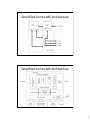
Simplified Cortex-M3 Architecture
Simplified Cortex-M3 Architecture
3
Cortex-M3 Processor Architecture
• Harvard architecture: it uses separate interfaces to
fetch instructions (Inst) and (Data)
• Processor is not memory starved: it permits accessing
data and instruction memories simultaneously
• From CM3 perspective, everything looks like memory
– Only differentiates between instruction fetches and data
accesses
• Interface between CM3 and manufacturer specific
hardware is through three memory buses:
– ICode, DCode, and System (for peripherals), which are
defined to access different regions of memory
Cortex-M3 Processor
• Cortex-M3 is a load/store architecture with
three basic types of instructions
• register-to-register operations for
processing data
• memory operations which move data
between memory and registers
• control flow operations enabling
programming language control flow such as
if and while statements and procedure calls
4
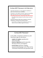
Cortex-M3 Pipeline
Instruction Prefetch & Execution
5
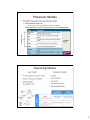
Processor Modes
Operating Modes
6
Exceptions
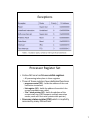
Processor Register Set
• Cortex-M3 core has 16 user-visible registers
– All processing takes place in these registers
• Three of these registers have dedicated functions
– program counter (PC) - holds the address of the next
instruction to execute
– link register (LR) - holds the address from which the
current procedure was called
– “the” stack pointer (SP) - holds the address of the
current stack top (CM3 supports multiple execution
modes, each with their own private stack pointer).
• Processor status register (PSR) which is implicitly
accessed by many instructions
7
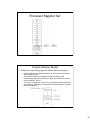
Processor Register Set
Program Memory Model
• RAM for an executing program is divided into three regions
– Data in RAM are allocated during the link process and initialized by
startup code at reset
– The (optional) heap is managed at runtime by library code
implementing functions such as the malloc and free which are part
of the standard C library
– The stack is managed at runtime by compiler generated code which
generates per-procedure-call stack frames containing local variables
and saved registers
8
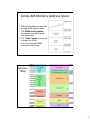
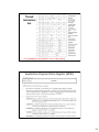
Cortex-M3 Memory Address Space
• ARM Cortex-M3 processor has
a single 4 GB address space
• The SRAM and Peripheral
areas are accessed through
the System bus
• The “Code” region is accessed
through the ICode
(instructions) and DCode
(constant data) buses
Memory
Map
9
Instruction Set Architecture (ISA)
• Instruction set
– Addressing modes
– Word size
– Data formats
– Operating modes
– Condition codes
Major Elements of ISA
32-bits
32-bits
mov r0, #1
ld
r1, [r0,#5]
r1=mem((r0)+5)
bne loop
subs r2, #1
Endianess
Endianess
10
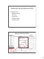
Addressing: Big Endian vs Little Endian
• Endian-ness: ordering of bytes within a word
– Little - increasing numeric significance with increasing memory
addresses
– Big – The opposite, most significant byte first
– MIPS is big endian, x86 is little endian
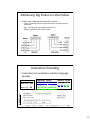
Instruction Encoding
• Instructions are encoded in machine language
opcodes
Instructions
movs r0, #10
ARMv7 ARM
movs r1, #0
Register Value
Memory Value
001|00|000|00001010 (LSB) (MSB)
(msb)
(lsb) 0a 20 00 21
001|00|001|00000000
11
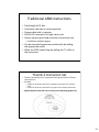
Traditional ARM instructions
•
•
•
•
•
Fixed length of 32 bits
Commonly take two or three operands
Process data held in registers
Shift & ALU operation in single clock cycle
Access memory with load and store instructions only
– Load/Store multiple register
• Can be extended to execute conditionally by adding
the appropriate suffix
• Affect the CPSR status flags by adding the ‘S’ suffix to
the instruction
Thumb-2 Instruction Set
• Thumb-2 instruction set is a superset of the previous 16-bit Thumb
instruction set
• Provides
– A large set of 16-bit instructions, enabling 2 instructions per memory
fetch
– A small set of 32-bit instructions to support more complex operations
• Specific details of this ISA not our focus (we’ll mostly program in C)
12
16bit Thumb-2
• Some of the changes used to reduce the length of the
instructions from 32 bits to 16 bits
– reduce the number of bits used to identify the register
• less number of registers can be used
– reduce the number of bits used for the immediate value
• smaller number range
– remove options such as ‘S’
• make it default for some instructions
– remove conditional fields (N, Z, V, C)
– no conditional executions (except branch)
– remove the optional shift (and no barrel shifter operation
• introduce dedicated shift instructions
– remove some of the instructions
• more restricted coding
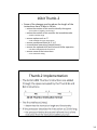
Thumb-2 Implementation
13
32bit Instruction Encoding
ARM and 16-bit Instruction Encoding
14
Thumb
Instruction
Set
•
See 4_THUMB_Instr_Set_pt3.pdf included in lab1_files.zip
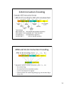
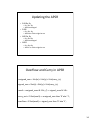
Application Program Status Register (APSR)
15
Updating the APSR
• SUB Rx, Ry
– Rx = Rx - Ry
– APSR unchanged
• SUBS
– Rx = Rx - Ry
– APSR N or Z bits might be set
• ADD Rx, Ry
– Rx = Rx + Ry
– APSR unchanged
• ADDS
– Rx = Rx + Ry
– APSR C or V bits might be set
Overflow and Carry in APSR
unsigned_sum = UInt(x) + UInt(y) + UInt(carry_in);
signed_sum = SInt(x) + SInt(y) + UInt(carry_in);
result = unsigned_sum<N-1:0>; // == signed_sum<N-1:0>
carry_out = if UInt(result) == unsigned_sum then ’0’ else ’1’;
overflow = if SInt(result) == signed_sum then ’0’ else ’1’;
16
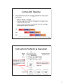
Conditional Execution
Conditional Execution
17
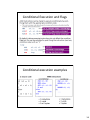
Conditional Execution and Flags
Conditional execution examples
18
ARM Instruction Set
Data Processing Instructions
• Arithmetic and logical operations
• 3-address format:
– Two 32-bit operands (op1 is register, op2 is
register or immediate)
– 32-bit result placed in a register
• Barrel shifter for op2 allows full 32-bit shift
within instruction cycle
19
Data Processing Instructions
• Arithmetic operations:
– ADD, ADDC, SUB, SUBC, RSB, RSC
• Bit-wise logical operations:
– AND, EOR, ORR, BIC
• Register movement operations:
– MOV, MVN
• Comparison operations:
– TST, TEQ, CMP, CMN
Data Processing Instructions
20
Data Processing Instructions
Multiply Instructions
•
•
•
•
Integer multiplication (32-bit result)
Long integer multiplication (64-bit result)
Built in Multiply Accumulate Unit (MAC)
Multiply and accumulate instructions add
product to running total
21
Multiply Instructions
Data Transfer Instructions
•
•
•
•
Load/store instructions
Used to move signed and unsigned
Word, Half Word and Byte to and from registers
Can be used to load PC (if target address is beyond
branch instruction range)
22
Addressing Modes
• Offset Addressing
– Offset is added or subtracted from base register
– Result used as effective address for memory access
– [<Rn>, <offset>]
• Pre-indexed Addressing
–
–
–
–
Offset is applied to base register
Result used as effective address for memory access
Result written back into base register
[<Rn>, <offset>]!
• Post-indexed Addressing
– The address from the base register is used as the EA
– The offset is applied to the base and then written back
– [<Rn>], <offset>
<offset> options
• An immediate constant
– #10
• An index register
– <Rm>
• A shifted index register
– <Rm>, LSL #<shift>
23
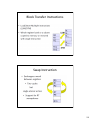
Block Transfer Instructions
Swap Instruction
24
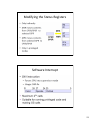
Modifying the Status Registers
Software Interrupt
25
Branching Instructions
• Branch (B):
– jumps forwards/backwards up to 32 MB
• Branch link (BL):
– same + saves (PC+4) in LR
• Suitable for function call/return
• Condition codes for conditional branches
Branching Instructions
26
IF-THEN Instruction
Barrier instructions
27
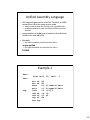
Unified Assembly Language
• UAL supports generation of either Thumb-2 or ARM
instructions from the same source code
– same syntax for both the Thumb code and ARM code
– enable portability of code for different ARM processor
families
• Interpretation of code type is based on the directive
listed in the assembly file
• Example:
– For GNU Assembler, the directive for UAL is
.syntax unified
– For ARM assembler, the directive for UAL is
THUMB
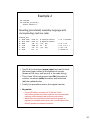
Example 1
data:
.byte 0x12, 20, 0x20, -1
func:
top:
mov r0,
mov r4,
movw
movt
ldrb
add r4,
add r0,
cmp r0,
bne top
#0
#0
r1,
r1,
r2,
r4,
r0,
#4
#:lower16:data
#:upper16:data
[r1],1
r2
#1
28
From ARM
Architecture
Reference Manual
There are similar entries for
move immediate, move shifted
(which actually maps to different
instructions) etc.
29
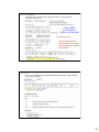
Example 2
int counter;
int Counter_Inc(void) {
return counter ++;
}
Resulting (annotated) assembly language with
corresponding machine code:
Counter_Inc:
0: f240 0300
4: f2c0 0300
8: 6818
a: 1c42
c: 601a
e: 4740
movw
movt
ldr
adds
str
bx
r3
r3
r0
r2
r2
lr
,
,
,
,
,
#:lower16:counter
#:upper16:counter
[r3 , #0]
r0 , #1
[r3 , #0]
// r3 = &counter
//
//
//
//
r0 = *r3
r2 = r0 + 1
*r3 = r2
return r0
• Two 32-bit instructions (movw, movt) are used to load
the lower/upper halves of the address of counter
(known at link time, and hence 0 in the code listing)
• Then, three 16-bit instructions load (ldr) the value of
counter, increment (adds) the value, and write back
(str) the updated value
• Finally, the procedure returns the original counter
• Key points:
– Cortex-M3 utilizes a mixture of 32-bit and 16-bit
instructions (mostly the latter) and the core interacts with
memory solely through load and store instructions
– While there are instructions that load/store groups of
registers (in multiple cycles) there are no instructions that
directly operate on memory locations
30
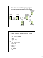
How does an assembly language program
get turned into a executable program image?
Binary program
file (.bin)
Assembly
files (.s)
Object
files (.o)
as
(assembler)
Executable
image file
ld
(linker)
Memory
layout
Linker
script (.ld)
Disassembled
code (.lst)
An ARM assembly language program for GNU
.equ
.text
.syntax
.thumb
.global
.type
STACK_TOP, 0x20000800
.word
STACK_TOP, start
unified
_start
start, %function
_start:
start:
movs r0, #10
movs r1, #0
loop:
adds
subs
bne
deadloop:
b
.end
r1, r0
r0, #1
loop
deadloop
31
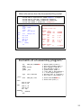
What information does the disassembled file provide?
all:
arm-none-eabi-as -mcpu=cortex-m3 -mthumb example1.s -o example1.o
arm-none-eabi-ld -Ttext 0x0 -o example1.out example1.o
arm-none-eabi-objcopy -Obinary example1.out example1.bin
arm-none-eabi-objdump -S example1.out > example1.lst
.equ
.text
.syntax
.thumb
.global
.type
STACK_TOP, 0x20000800
.word
STACK_TOP, start
example1.out:
file format elf32-littlearm
unified
Disassembly of section .text:
_start
start, %function
_start:
start:
movs r0, #10
movs r1, #0
00000000 <_start>:
0:
20000800
4:
00000009
.word
.word
0x20000800
0x00000009
00000008 <start>:
8:
200a
a:
2100
movs
movs
r0, #10
r1, #0
0000000c <loop>:
c:
1809
e:
3801
10:
d1fc
adds
subs
bne.n
r1, r1, r0
r0, #1
c <loop>
loop:
adds r1, r0
subs r0, #1
bne loop
deadloop:
b
deadloop
.end
00000012 <deadloop>:
12:
e7fe
b.n
12 <deadloop>
Elements of an assembly program?
.equ
STACK_TOP, 0x20000800
.text
.syntax unified
.thumb
.global _start
.type
start, %function
.word
STACK_TOP, start
/*
/*
/*
/*
/*
/*
/*
/*
/*
Equates symbol to value */
Tells AS to assemble region */
Means language is ARM UAL */
Means ARM ISA is Thumb */
.global exposes symbol */
_start label is the beginning */
...of the program region */
Specifies start is a function */
start label is reset handler */
_start:
/* Inserts word 0x20000800 */
/* Inserts word (start) */
start:
movs r0, #10
movs r1, #0
loop:
adds
subs
bne
deadloop:
b
.end
r1, r0
r0, #1
loop
deadloop
32
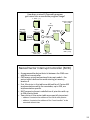
How does a mixed C/Assembly program
get turned into a executable program image?
C files (.c)
ld
(linker)
Assembly
files (.s)
Object
files (.o)
as
(assembler)
Binary program
file (.bin)
Executable
image file
gcc
(compile
+ link)
Memory
layout
Library object
files (.o)
Linker
script (.ld)
Disassembled
Code (.lst)
Nested Vector Interrupt Controller (NVIC)
• A programmable device that sits between the CM3 core
and the microcontroller
• CM3 uses a prioritized vectored interrupt model – the
vector table is defined to reside starting at memory
location 0
• First 16 entries in this table are defined for all Cortex-M3
implementations while the remainder, up to 240, are
implementation specific
• NVIC supports dynamic redefinition of priorities with up
to 256 priority levels
• Two entries in the vector table are especially important:
– address 0 contains the address of the initial stack pointer
– address 4 contains the address of the “reset handler” to be
executed at boot time
33
Nested Vector Interrupt Controller (NVIC)
• Provides key system control registers including the
System Timer (SysTick) that provides a regular timer
interrupt
• Provision for a built-in timer across the Cortex-M3
family has the significant advantage of making
operating system code highly portable – all operating
systems need at least one core timer for time-slicing
• Registers used to control the NVIC are defined to reside
at address 0xE000E000 and are defined by the CortexM3 specification
• These registers are accessed with the system bus
Outline
• ARM Cortex-M3 processor
• NXP LPC17xx microcontroller unit (MCU)
34
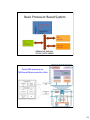
Basic Processor Based System
Cortex-M3 processor vs.
CM3-based Microcontroller Units
35
While there is significant overlap between the families and
their peripherals, there are also important differences
In the lab of this course we focus on the NXP’s LPC17xx family
LPC17xx
• LPC17xx (of NXP) is an ARM Cortex-M3 based microcontroller
• The Cortex-M3 is also the basis for microcontrollers from other
manufacturers including TI, ST, Toshiba, Atmel, etc.
• LPC1768 operates at up to a 100 MHz CPU frequency
• Sophisticated clock system
• Peripherals include:
–
–
–
–
–
–
–
–
–
–
–
up to 512 kB of flash memory, up to 64 kB of data memory
Ethernet MAC
a USB interface that can be configured as either Host, Device, or OTG
8 channel general purpose DMA controller
4 UARTs, 2 CAN channels, 2 SSP controllers, SPI interface
3 I2C interfaces, 2-input plus 2-output I2S interface
8 channel 12-bit ADC, 10-bit DAC, motor control PWM
Quadrature Encoder interface, 4 general purpose timers,
6-output general purpose PWM
ultra-low power RTC with separate battery supply
up to 70 general purpose I/O pins
36
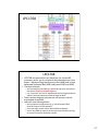
LPC1768
LPC1768
• LPC1768 microcontrollers are based on the Cortex-M3
processor with a set of peripherals distributed across three
buses – Advanced High-performance Bus (AHB) and its two
Advanced Peripheral Bus (APB) sub-buses APB1 and APB2.
• These peripherals:
– are controlled by the CM3 core with load and store instructions
that access memory mapped registers
– can “interrupt” the core to request attention through peripheral
specific interrupt requests routed through the NVIC
• Data transfers between peripherals and memory can be
automated using DMA
• Labs will cover among others:
– basic peripheral configuration (e.g., lab1 illustrates GPIO
General Purpose I/O peripherals)
– how interrupts can be used to build effective software
– how to use DMA to improve performance and allow processing
to proceed in parallel with data transfer
37
LPC1768
•
Peripherals are “memory-mapped”
– core interacts with the peripheral hardware by reading and writing peripheral
“registers” using load and store instructions
•
The various peripheral registers are documented in the user and reference
manuals
– documentation include bit-level definitions of the various registers and info on
how interpret those bits
– actual physical addresses are also found in the reference manuals
•
Examples of base addresses for several peripherals (see page 14 of the
LPC17xx user manual):
0x40010000
0x40020000
0x40028000
0x40034000
…
•
UART1
SPI
GPIO interrupts
ADC
No real need for a programmer to look up all these values as they are
defined in the library file lpc17xx.h as:
LPC_UART1_BASE
LPC_SPI_BASE
LPC_GPIOINT_BASE
LPC_ADC_BASE
…
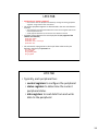
LPC1768
• Typically, each peripheral has:
• control registers to configure the peripheral
• status registers to determine the current
peripheral status
• data registers to read data from and write
data to the peripheral
38
LPC1768
• In addition to providing the addresses of the
peripherals, lpc17xx.h also provides C language level
structures that can be used to access each peripheral.
• For example, the SPI and GPIO ports are defined by the
following register structures:
typedef struct
{
__IO uint32_t SPCR;
__I uint32_t SPSR;
__IO uint32_t SPDR;
__IO uint32_t SPCCR;
uint32_t RESERVED0[3];
__IO uint32_t SPINT;
} LPC_SPI_TypeDef;
LPC1768
typedef struct
{
union {
__IO uint32_t FIODIR;
struct {
__IO uint16_t FIODIRL;
__IO uint16_t FIODIRH;
};
struct {
__IO uint8_t FIODIR0;
__IO uint8_t FIODIR1;
__IO uint8_t FIODIR2;
__IO uint8_t FIODIR3;
};
};
uint32_t RESERVED0[3];
union {
__IO uint32_t FIOMASK;
struct {
__IO uint16_t FIOMASKL;
__IO uint16_t FIOMASKH;
};
struct {
__IO uint8_t FIOMASK0;
__IO uint8_t FIOMASK1;
__IO uint8_t FIOMASK2;
__IO uint8_t FIOMASK3;
};
};
union {
__IO uint32_t FIOPIN;
struct {
__IO uint16_t FIOPINL;
__IO uint16_t FIOPINH;
};
struct {
__IO uint8_t FIOPIN0;
__IO uint8_t FIOPIN1;
__IO uint8_t FIOPIN2;
__IO uint8_t FIOPIN3;
};
};
union {
__IO uint32_t FIOSET;
struct {
__IO uint16_t FIOSETL;
__IO uint16_t FIOSETH;
};
struct {
__IO uint8_t FIOSET0;
__IO uint8_t FIOSET1;
__IO uint8_t FIOSET2;
__IO uint8_t FIOSET3;
};
};
union {
__O uint32_t FIOCLR;
struct {
__O uint16_t FIOCLRL;
__O uint16_t FIOCLRH;
};
struct {
__O uint8_t FIOCLR0;
__O uint8_t FIOCLR1;
__O uint8_t FIOCLR2;
__O uint8_t FIOCLR3;
};
};
} LPC_GPIO_TypeDef;
39
LPC1768
• The register addresses of the various ports are defined in
the library (see lpc17xx.h):
#define
…
#define
#define
#define
#define
…
#define
…
LPC_APB0_BASE
(0x40000000UL)
LPC_UART1_BASE
LPC_SPI_BASE
LPC_GPIOINT_BASE
LPC_ADC_BASE
(LPC_APB0_BASE
(LPC_APB0_BASE
(LPC_APB0_BASE
(LPC_APB0_BASE
LPC_GPIO1
+
+
+
+
0x10000)
0x20000)
0x28080)
0x34000)
((LPC_GPIO_TypeDef *) LPC_GPIO1_BASE)
• For example, to turn on LED P1.29 on the development
board, the following code can be used:
LPC_GPIO1->FIOSET = 1 << 29;
Memory
• On-chip flash memory system
– Up to 512 kB of on-chip flash memory
– Flash memory accelerator maximizes performance for
use with the two fast AHB-Lite buses
– Can be used for both code and data storage
• On-chip Static RAM
– Up to 64 kB of on-chip static RAM memory
– Up to 32 kB of SRAM, accessible by the CPU and all
three DMA controllers are on a higher-speed bus
– Devices with more than 32 kB SRAM have two
additional 16 kB SRAM blocks
40
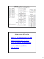
LPC17xx system memory map
References & Credits
• Joseph Jiu, The Definitive guide to the ARM
Cortext-M3, 2007
• LPC17xx microcontroller user manual
• Cortex-M3 Processor Technical Reference
Manual
• Lab manual (G. Brown, Indiana)
• EECS 373, UMich
41