1
EE-379 Embedded Systems and Applications
Memory Revisited
Cristinel Ababei
Department of Electrical Engineering, University at Buffalo
Spring 2013
Note: This course is offered as EE 459/500 in Spring 2013
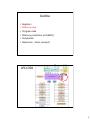
Outline
•
•
•
•
•
•
Registers
Memory map
Program code
Memory protection unit (MPU)
Peripherals
Memories – basic concepts
1
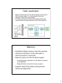
Cortex-M3
• Cortex-M3, as a RISC processor, is a load/store
architecture with three basic types of
instructions:
– Register-to-register operations for processing data
– Memory operations which move data between
memory and registers
– Control flow operations enabling programming
language control flow such as if and while
statements and procedure calls
Processor Register Set
• Cortex-M3 core has 16 user-visible registers
– All processing takes place in these registers!
• Three of these registers have dedicated functions
– program counter (PC) - holds the address of the next
instruction to execute
– link register (LR) - holds the address from which the
current procedure was called
– “the” stack pointer (SP) - holds the address of the
current stack top (CM3 supports multiple execution
modes, each with their own private stack pointer).
• Processor Status Register (PSR) which is implicitly
accessed by many instructions
2
Processor Register Set
Special Registers
3
Outline
•
•
•
•
•
•
Registers
Memory map
Program code
Memory protection unit (MPU)
Peripherals
Memories – basic concepts
LPC1768
4
Memory
• On-chip Flash memory system
– Up to 512 kB of on-chip flash memory
– Flash memory accelerator maximizes performance for
use with the two fast advanced high-performance bus
AHB-Lite buses
– Can be used for both code and data storage
• On-chip Static RAM (SRAM)
– Up to 64 kB of on-chip static RAM memory
– Up to 32 kB of SRAM, accessible by the CPU and all
three DMA (direct memory access) controllers are on
a higher-speed bus
– Devices with more than 32 kB SRAM have two
additional 16 kB SRAM blocks
LPC1768 – Flash memory – dynamic
characteristics
5
Flash accelerator
• Allows maximization of the performance of the CortexM3 processor when it is running code from flash
memory, while also saving power
• The flash accelerator also provides speed and power
improvements for data accesses to the flash memory
Memory
• Predefined (fixed) memory map that specifies
which bus interface is to be used when a
memory location is accessed
• Memory system has the bit-band support
• Provides atomic operations to bit data in memory
or peripherals
• Supported only in special memory regions
• Supports both little endian and big endian
memory configuration
6
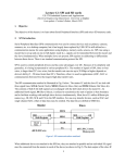
Cortex-M3 Memory Address Space (1)
• ARM Cortex-M3 has a single
“physical” address space of 232
bytes (4 GB)
• ARM Cortex-M3 Technical
Reference Manual defines how
this address space is to be used
(predefined memory map)
• The SRAM and Peripheral areas
are accessed through the System
bus
• The “Code” region is accessed
through the ICode (instructions)
and DCode (constant data) buses
Memory
Map (2)
7
Memory Map (3)
Outline
•
•
•
•
•
•
Registers
Memory map
Program code
Memory protection unit (MPU)
Peripherals
Memories – basic concepts
8
Program Memory Model
• Cortex-M3 has been designed to be programmed (almost) entirely
in high programming languages (e.g., C)
• So, it has a well developed “procedure call standard” (called an ABI
or application binary interface) which dictates how registers are
used
• This model explicitly assumes that the RAM for an executing
program is divided into three regions:
Program Memory Model
• RAM for an executing program is divided into three
regions:
– Data in RAM are allocated during the link process and
initialized by startup code at reset
– The (optional) heap is managed at runtime by library
code implementing functions such as the malloc and
free which are part of the standard C library
– The stack is managed at runtime by compiler generated
code which generates per-procedure-call stack frames
containing local variables and saved registers
9
Program code
• Program code can be located in:
– the Code region
– the SRAM region
– the External RAM region
• It is best to put the program code in the Code
region because the instruction fetches and
data accesses are carried out simultaneously
on two separate bus interfaces
Outline
•
•
•
•
•
•
Registers
Memory map
Program code
Memory protection unit (MPU)
Peripherals
Memories – basic concepts
10
Memory Protection Unit (MPU)
• Cortex-M3 has an optional Memory Protection Unit
(MPU). LPC1768 has one that supports 8 regions.
– Allows access rules to be set up for privileged access and
user program access
– When an access rule is violated -> a fault exception is
generated -> fault exception handler will be able to analyze
the problem and correct it if possible
• MPU can be used in various ways
– Set up by an operating system, allowing data used by
privileged code (e.g., the operating system kernel) to be
protected from untrusted user programs
– Can be used to make memory regions read-only, to
prevent accidental erasing of data, or to isolate memory
regions between different tasks in a multitasking system
• Overall, it can help make embedded systems more
robust and reliable
Outline
•
•
•
•
•
•
Registers
Memory map
Program code
Memory protection unit (MPU)
Peripherals
Memories – basic concepts
11
Peripherals
• LPC1768 microcontrollers are based on the Cortex-M3
processor with a set of peripherals distributed across three
buses – Advanced High-performance Bus (AHB) and its two
Advanced Peripheral Bus (APB) sub-buses APB1 and APB2.
• These peripherals:
– are controlled by the CM3 core with load and store instructions
that access memory mapped registers
– can “interrupt” the core to request attention through peripheral
specific interrupt requests routed through the NVIC
• Data transfers between peripherals and memory can be
automated using DMA
• Labs will cover among others:
– basic peripheral configuration (e.g., lab1 illustrates GPIO
General Purpose I/O peripherals)
– how interrupts can be used to build effective software
– how to use DMA to improve performance and allow processing
to proceed in parallel with data transfer
Peripherals
•
Peripherals are “memory-mapped”
– core interacts with the peripheral hardware by reading and writing peripheral
“registers” using load and store instructions
•
The various peripheral registers are documented in the user and reference
manuals
– documentation include bit-level definitions of the various registers and info on
how interpret those bits
– actual physical addresses are also found in the reference manuals
•
Examples of base addresses for several peripherals (see page 14 of the
LPC17xx user manual):
0x40010000
0x40020000
0x40028000
0x40034000
…
•
UART1
SPI
GPIO interrupts
ADC
No real need for a programmer to look up all these values as they are
defined in the library file lpc17xx.h as:
LPC_UART1_BASE
LPC_SPI_BASE
LPC_GPIOINT_BASE
LPC_ADC_BASE
…
12
Peripherals
• Typically, each peripheral has:
• control registers to configure the peripheral
• status registers to determine the current
peripheral status
• data registers to read data from and write
data to the peripheral
Peripherals
• In addition to providing the addresses of the
peripherals, lpc17xx.h also provides C language level
structures that can be used to access each peripheral.
• For example, the SPI and GPIO ports are defined by the
following register structures:
typedef struct
{
__IO uint32_t SPCR;
__I uint32_t SPSR;
__IO uint32_t SPDR;
__IO uint32_t SPCCR;
uint32_t RESERVED0[3];
__IO uint32_t SPINT;
} LPC_SPI_TypeDef;
13
Outline
•
•
•
•
•
•
Registers
Memory map
Program code
Memory protection unit (MPU)
Peripherals
Memories – basic concepts
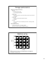
Memory: basic concepts
• Stores large number of bits
m x n: m words of n bits each
k = Log2(m) address input signals
or m = 2k words
e.g., 4,096 x 8 memory:
m × n memory
…
m words
–
–
–
–
…
• 32,768 bits
• 12 address input signals
• 8 input/output data signals
• Memory access
– r/w: selects read or write
– enable: read or write only when
asserted
– multiport: multiple accesses to different
locations simultaneously
n bits per word
memory external view
r/w
2k × n read and
write memory
enable
A0
…
Ak-1
…
Qn-1
Q0
14
Memory: basic categories
Writable?
• Read-Only Memory (ROM):
– Can only be read; cannot be modified (written) by the processor.
Contents of ROM chip are set before chip is placed into the
system.
•
Random-Access Memory (RAM):
– Read/write memory. Although technically inaccurate, term is
used for historical reasons. (ROMs are also random access.)
Permanence?
• Volatile memories
– Lose their contents when power is turned off. Typically used to
store program while system is running.
•
Non-volatile memories do not.
– Required by every system to store instructions that get executed
when system powers up (boot code).
Memories classification
Read-Write Memory
Volatile Memory
Random Access
Read-Only Memory
Non-volatile
Memory
Sequential Access
Mask-Programmed ROM (PROM)
EPROM
(nonvolatile)
FIFO
EEPROM
SRAM
LIFO
FLASH
DRAM
Shift Register
CAM
Volatile: need electrical power
Nonvolatile: magnetic disk, retains its stored information after the removal of power
Random access: memory locations can be read or written in a random order
EPROM: erasable programmable read-only memory
EEPROM: electrically erasable programmable read-only memory
FLASH: memory stick, USB disk
Access pattern: sequential access: (video memory streaming) first-in-first-out (buffer), last-in-first-out
(stack), shift register, content-addressable memory
Static vs. Dynamic: dynamic needs periodic refresh but is simpler, higher density
Key Design Metrics:
1.Memory Density (number of bits/mm2) and Size
2.Access Time (time to read or write) and Throughput
3.Power Dissipation
15
Memories classification
Memory Arrays
Random Access Memory
Read/Write Memory
(RAM)
(Volatile)
Static RAM
(SRAM)
Dynamic RAM
(DRAM)
Mask ROM
Programmable
ROM
(PROM)
Content Addressable Memory
(CAM)
Serial Access Memory
Read Only Memory
(ROM)
(Nonvolatile)
Shift Registers
Serial In
Parallel Out
(SIPO)
Erasable
Programmable
ROM
(EPROM)
Queues
Parallel In
Serial Out
(PISO)
Electrically
Erasable
Programmable
ROM
(EEPROM)
First In
First Out
(FIFO)
Last In
First Out
(LIFO)
Flash ROM
Write-ability and Storage-permanence
•
Traditional ROM/RAM distinctions
– ROM
• read only, bits stored without power
– RAM
• read and write, lose stored bits without power
•
Traditional distinctions blurred
– Advanced ROMs can be written to
• e.g., EEPROM
– Advanced RAMs can hold bits without power
• e.g., NVRAM
•
Write ability
•
Storage permanence
– Manner and speed a memory can be written
– Ability of memory to hold stored bits after they are written
16
Storage
permanence
Write-ability and Storage-permanence
Mask-programmed ROM
Ideal memory
OTP ROM
Life of
product
EPROM
Tens of
years
Battery
life (10
years)
EEPROM
FLASH
NVRAM
Nonvolatile
In-system
programmable
Near
zero
SRAM/DRAM
Write
ability
During
External
External
External
External
fabrication programmer, programmer, programmer programmer
1,000s
OR in-system, OR in-system,
only
one time only
1,000s
block-oriented
of cycles
writes, 1,000s
of cycles
of cycles
In-system, fast
writes,
unlimited
cycles
Write ability and storage permanence of memories,
showing relative degrees along each axis (not to scale)
Write-ability
• Ranges of write ability
– High end
• processor writes to memory simply and quickly
• e.g., RAM
– Middle range
• processor writes to memory, but slower
• e.g., FLASH, EEPROM
– Lower range
• special equipment, “programmer”, must be used to write to memory
• e.g., EPROM, OTP ROM
– Low end
• bits stored only during fabrication
• e.g., Mask-programmed ROM
• In-system programmable memory
– Can be written to by a processor in the microcomputer system using
the memory
– Memories in high end and middle range of write ability
17
Storage-permanence
• Range of storage permanence
– High end
• essentially never loses bits
• e.g., mask-programmed ROM
– Middle range
• holds bits days, months, or years after memory’s power source turned off
• e.g., NVRAM
– Lower range
• holds bits as long as power supplied to memory
• e.g., SRAM
– Low end
• begins to lose bits almost immediately after written – refreshing needed
• e.g., DRAM
• Nonvolatile memory
– Holds bits after power is no longer supplied
– High end and middle range of storage permanence
Memory array
word
lines
Mem
Cell
Mem
Cell
Mem
Cell
Mem
Cell
Mem
Cell
Mem
Cell
Mem
Cell
Mem
Cell
Mem
Cell
Mem
Cell
Mem
Cell
Mem
Cell
Mem
Cell
Mem
Cell
Mem
Cell
Mem
Cell
bit lines
Different memory types are distinguished by technology for
storing bit in memory cell.
18
A0
A1
A2
A3
2 to 4 decoder
Support circuitry
memory
array
16 bits (4x4)
4:1 mux/demux
OE#
CS#
WE#
D0
Control signals:
• Control read/write of array
• Map internal physical array to external configuration (4x4 16x1)
Interface (1/2)
• Physical configurations are typically square.
– Minimize length word + bit line minimize access
delays.
• External configurations are “tall and narrow”.
The narrower the configuration, the higher the
pin efficiency. (Adding one address pin cuts data
pins in half.)
– Several external configurations available for a given
capacity.
– 64Kbits may be available as 64Kx1, 32Kx2, 16Kx4,…
19
Interface (2/2)
• Chip Select (CS#): Enables device. If not
asserted, device ignores all other inputs
(sometimes entering low-power mode).
• Write Enable (WE#): Store D0 at specified
address.
• Output Enable (OE#): Drive value at specified
address onto D0.
Memory timing: Reads
tRC
tAV
ADDR
CS#
OE#
tCS
tOE
DATA
•
Access time: Time required from start of a read access to valid data output.
– Access time specified for each of the three conditions required for valid data
output (valid address, chip select, output enable)
•
•
Time to valid data out depends on which of these is on critical path.
tRC: Minimum time required from start of one access to start of next.
– For most memories equal to access time.
20
Memory timing: Writes
tWC
tAW
ADDR
tCW
CS#
tWP
WE#
tAS
DATA
tDS
tDH
•
•
•
Write happens on rising edge of WE#
Separate access times tAW, tCW, tWP specified for address valid, CS#, WE#.
Typically, tAS = 0, meaning that WE# may not be asserted before address is
valid.
• Setup and hold times required for data.
• Write cycle time tWC is typically in the order of tAW.
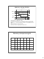
Memory Comparison grid
Memory
type
Read
speed
Write
speed
Volatility
density power
rewrite
SRAM
+++
+++
-
-
++
DRAM
+
+
--
++
EPROM
+
-
EEPROM
+
-
Flash
+
-
++
+
+
-
+
+
+
+
+
+
+
21
ROM: “Read-Only” Memory
External view
2k × n ROM
enable
A0
Ak-1
…
• Nonvolatile
• Can be read from but not written to, by a
processor in an microcomputer system
• Traditionally written to, “programmed”,
before inserting to microcomputer system
• Uses
…
– Store software program for general-purpose
processor
– Store constant data (parameters) needed by
system
– Implement combinational circuits (e.g., decoders)
Qn-1
Q0
Example: 8 x 4 ROM
•
•
•
•
Horizontal lines = words
Vertical lines = data
Lines connected only at circles
Decoder sets word 2’s line to 1 if
address input is 010
• Data lines Q3 and Q1 are set to 1
because there is a “programmed”
connection with word 2’s line
• Word 2 is not connected with data
lines Q2 and Q0
• Output is 1010
Internal view
8 × 4 ROM
enable
word 0
word 1
3×8
decoder
word 2
word line
A0
A1
A2
data line
programmable
connection
Q3
Q2 Q1 Q0
22
Mask-programmed ROM
• Connections “programmed” at fabrication
– set of masks
• Lowest write ability
– only once
• Highest storage permanence
– bits never change unless damaged
• Typically used for final design of high-volume systems
– spread out NRE (non-recurrent engineering) cost for a low unit cost
OTP ROM: One-time programmable ROM
• Connections “programmed” after manufacture by user
–
–
–
–
user provides file of desired contents of ROM
file input to machine called ROM programmer
each programmable connection is a fuse
ROM programmer blows fuses where connections should not exist
• Very low write ability
– typically written only once and requires ROM programmer device
• Very high storage permanence
– bits don’t change unless reconnected to programmer and more fuses
blown
• Commonly used in final products
– cheaper, harder to inadvertently modify
23
EPROM: UV Erasable programmable ROM
•
Programmable component is a MOS transistor
–
–
–
–
–
•
Transistor has “floating” gate surrounded by an insulator
(a) Negative charges form a channel between source and drain
storing a logic 1
(b) Large positive voltage at gate causes negative charges to
move out of channel and get trapped in floating gate storing a
logic 0
(c) (Erase) Shining UV rays on surface of floating-gate causes
negative charges to return to channel from floating gate
restoring the logic 1
(d) An EPROM package showing quartz window through which
UV light can pass
0V
floating gate
source
drain
(a)
+15V
(b)
source
drain
Better write ability
5-30 min
– can be erased and reprogrammed thousands of times
•
Reduced storage permanence
– program lasts about 10 years but is susceptible to
radiation and electric noise
•
Typically used during design development
source
drain
(c)
(d)
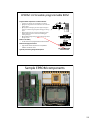
Sample EPROM components
24
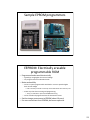
Sample EPROM programmers
EEPROM: Electrically erasable
programmable ROM
• Programmed and erased electronically
– typically by using higher than normal voltage
– can program and erase individual words
• Better write ability
– can be in-system programmable with built-in circuit to provide higher
than normal voltage
• built-in memory controller commonly used to hide details from memory user
– writes very slow due to erasing and programming
• “busy” pin indicates to processor EEPROM still writing
– can be erased and programmed tens of thousands of times
• Similar storage permanence to EPROM (about 10 years)
• Far more convenient than EPROMs, but more expensive
25
FLASH
• Extension of EEPROM
– Same floating gate principle
– Same write ability and storage permanence
• Fast erase
– Large blocks of memory erased at once, rather than one
word at a time
– Blocks typically several thousand bytes large
• Writes to single words may be slower
– Entire block must be read, word updated, then entire
block written back
FLASH applications
• Flash technology has made rapid advances in recent years.
– cell density rivals DRAM; better than EPROM; much better than
EEPROM.
– multiple gate voltages can encode 2 bits per cell.
– many-GB devices available
• ROMs and EPROMs rapidly becoming obsolete.
• Replacing hard disks in some applications.
– smaller, lighter, faster
– more reliable (no moving parts)
– cost effective
• PDAs, cell phones, laptops, iPods, etc…
26
RAM: “Random-Access” Memory
•
– bits are not held without power supply
•
•
external view
Typically volatile memory
r/w
2k × n read and write
memory
enable
A0
Read and written to easily by microprocessor
…
Ak-1
during execution
Internal structure more complex than ROM
…
Qn-1
– a word consists of several memory cells, each
storing 1 bit
– each input and output data line connects to each
cell in its column
– rd/wr connected to every cell
– when row is enabled by decoder, each cell has
logic that stores input data bit when rd/wr
indicates write or outputs stored bit when rd/wr
indicates read
Q0
internal view
I3 I2 I1 I0
4×4 RAM
enable
2×4
decoder
A0
A1
rd/wr
Memory
cell
To every cell
Q3 Q2 Q1 Q0
Basic types of RAM
• SRAM: Static RAM
– Memory cell uses flip-flop to store bit
– Requires 6 transistors
– Holds data as long as power supplied
• DRAM: Dynamic RAM
– Memory cell uses MOS transistor and
capacitor to store bit
– More compact than SRAM
– Retains data for only 2 – 4 ms
– “Refresh” required due to capacitor
leak
memory cell internals
SRAM
Data'
Data
W
DRAM
Data
W
• word’s cells refreshed when read
– Slower to access than SRAM
27
RAM variations
• PSRAM: Pseudo-static RAM
– DRAM with built-in memory refresh controller
– Popular low-cost high-density alternative to SRAM
• NVRAM: Nonvolatile RAM
– Holds data after external power removed
– Battery-backed RAM
• SRAM with own permanently connected battery
• writes as fast as reads
• no limit on number of writes unlike nonvolatile ROM-based memory
– SRAM with EEPROM or FLASH
• stores complete RAM contents on EEPROM or FLASH before power turned off
Dual-port RAM (DPRAM)
• Usually a static RAM circuit with two address
and data bus connections
– Shared RAM for two independent users
• Flexible communication link between two
processors
– Master/slave
28
DDR1 SDRAM, DDR2
• Double Data Rate synchronous dynamic random access
memory (DDR1 SDRAM) is a class of memory
integrated circuits used in computers.
• The interface uses double pumping (transferring data
on both the rising and falling edges of the clock signal)
to lower the clock frequency
• One advantage of keeping the clock frequency down is
that it reduces the signal integrity requirements on the
circuit board connecting the memory to the controller
• DDR2 memory is fundamentally similar to DDR SDRAM
• DDR2 SDRAM can perform four transfers per clock
using a multiplexing technique
Credits and references
• Joseph Jiu, The Definitive guide to the ARM
Cortext-M3, 2007 (Chapters 5,13)
• LPC17xx microcontroller user manual
• Cortex-M3 Processor Technical Reference
Manual
• Lab manual (G. Brown, Indiana)
• EECS 373, Umich
• http://esd.cs.ucr.edu
29