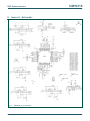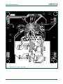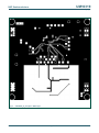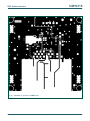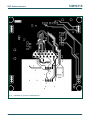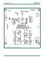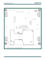
1
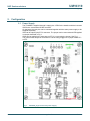
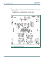
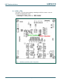
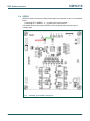
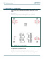
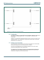
UM10319 Cake8026_02_D Rev. 1.0 — 4 August 2011 User manual Document information Info Content Keywords TDA8026, Demo Board Abstract This user manual describes how to use the Cake8026_02_D, a demo board used to evaluate the TDA8026 device, a 5 slots smart cards reader. UM10319 NXP Semiconductors Cake8026_02_D Revision history Rev Date Description 1.0 First version 20110804 Contact information For more information, please visit: http://www.nxp.com For sales office addresses, please send an email to: [email protected] UM10319 User manual All information provided in this document is subject to legal disclaimers. Rev. 1.0 — 4 August 2011 © NXP B.V. 2011. All rights reserved. 2 of 27 UM10319 NXP Semiconductors Cake8026_02_D 1. Introduction 1.1 TDA8026 The TDA8026 is a 5 slots smart card reader interface. It is mainly dedicated to Point-OfSales applications with one or two main slots for customer card and 4 or 3 extra slots for Secure Access Modules. 1.2 Cake8026_02_D The demo board Cake8026_02_D is an evaluation board for the TDA8026. It allows testing the main functionalities of the TDA8026. This board embeds all the mandatory components to design the TDA8026 so that the user just need to connect the interface with its host to start developing applications based on the TDA8026. On this demo board, the slot 1 can receive a general banking sized smart card while the slots from 2 to 5 have SIM-sized smart card connectors. UM10319 User manual All information provided in this document is subject to legal disclaimers. Rev. 1.0 — 4 August 2011 © NXP B.V. 2011. All rights reserved. 3 of 27 UM10319 NXP Semiconductors Cake8026_02_D 2. Configuration 2.1 Power Supply The TDA8026 is supplied through 2 supply pins: VDDI for the interface with the host and VDD for the core and the DCDC converter. On the board, the two pins can be connected together with the same power supply or be supplied separately. VDD can be input by the ST13 connector. The jumper can be removed and VDD applied on the pin described in Fig 1. VDDI can be applied in the same way on ST12, by removing the jumper. See Fig 1. The ground must always be connected. It can be easily plugged on a jumper called ST1 or ST2. Fig 1. UM10319 User manual Cake8026_02_D connect the power supply All information provided in this document is subject to legal disclaimers. Rev. 1.0 — 4 August 2011 © NXP B.V. 2011. All rights reserved. 4 of 27 UM10319 NXP Semiconductors Cake8026_02_D 2.2 A0 A0 allows choosing the I²C address. It can be fixed by hardware thanks to the soldering points ST8 and ST9. Connecting ST8: A0 = 1. TDA8026’s addresses = 4Ch, 44h and 46h. Connecting ST9: A0 = 0. TDA8026’s addresses = 48h, 40h and 42h. Fig 2. UM10319 User manual Cake8026_02_D A0 configuration All information provided in this document is subject to legal disclaimers. Rev. 1.0 — 4 August 2011 © NXP B.V. 2011. All rights reserved. 5 of 27 UM10319 NXP Semiconductors Cake8026_02_D 2.3 DCDC_CTRL The DCDC_CTRL pin allows enabling or disabling the DCDC converter. It can be selected by soldering ST5 or ST7. Connecting ST5: DCDC_CTRL = 1 DCDC disabled Connecting ST7: DCDC_CTRL = 0 DCDC enabled Fig 3. UM10319 User manual Cake8026_02_D DCDC_CTRL configuration All information provided in this document is subject to legal disclaimers. Rev. 1.0 — 4 August 2011 © NXP B.V. 2011. All rights reserved. 6 of 27 UM10319 NXP Semiconductors Cake8026_02_D 2.4 SPRES SPRES is used to choose the polarity of the smart card connector on slot 1, as described below: Connecting ST10: SPRES = 1 normally closed card connector Connecting ST11: SPRES = 0 normally open card connector The default value for this board is SPRES = 0 as the default card connector type is normally open. Fig 4. UM10319 User manual Cake8026_02_D SPRES configuration All information provided in this document is subject to legal disclaimers. Rev. 1.0 — 4 August 2011 © NXP B.V. 2011. All rights reserved. 7 of 27 UM10319 NXP Semiconductors Cake8026_02_D 3. Connection to the host To start using the TDA, a few wires are required. Then the other wires can be added to evaluate more features of the TDA8026. The following tables give a summary of the connections to make in order to achieve a specific goal. Please note: The ground connection is not mentioned in the tables but shall always be connected between the host board and the Cake8026_02_D board. Table 1. Connection to access the TDA8026´ registers Cake8026 pin Host connection Cake 8026 pin position VDD = VDDI Microcontroller power supply J3-1 and J2-1 or VDD and VDDI test pin. SDA Master I²C SDA pin J1-1 or SDA test pin SCL Master I²C SCL pin J1-3 or SCL test pin TDA8026 application example Read the product version. Check the pending interrupts. Check the card presence. See Table 6 in chapter 5: TDA8026 application examples Table 2. Access slot 1 Cake8026 pin Host connection VDD = VDDI Microcontroller power supply Cake8026 pin position TDA8026 application example J3-1 and J2-1 or VDD and Activate the smart card. VDDI test pin. SDA Master I²C SDA pin J1-1 or SDA test pin SCL Master I²C SCL pin J1-3 or SCL test pin IOUC1 Host’s ISO 7816 UART I/O line J2-3 or IOUC1 test pin Host’s ISO 7816 UART J2-5 or CLKIN1 pin CLKIN1 CLK line UM10319 User manual All information provided in this document is subject to legal disclaimers. Rev. 1.0 — 4 August 2011 Receive the ATR. Send an APDU and receive the answer. See Table 7 in chapter 5: TDA8026 application examples © NXP B.V. 2011. All rights reserved. 8 of 27 UM10319 NXP Semiconductors Cake8026_02_D Table 3. Access slots 1 to 5 Cake8026 pin Host connection Cake8026 pin position VDD = VDDI Microcontroller power supply J3-1 and J2-1 or VDD and VDDI test pin. SDA Master I²C SDA pin J1-1 or SDA test pin SCL Master I²C SCL pin J1-3 or SCL test pin IOUC1 Host’s ISO 7816 UART I/O line J2-3 or IOUC1 test pin CLKIN1 Host’s ISO 7816 UART CLK line J2-5 or CLKIN1 pin IOUC2 Host’s ISO 7816 UART I/O line (IOUC1 and IOUC2 can be connected together) J1-5 or IOUC2 test pin Host’s ISO 7816 UART CLK line (CLKIN1 and CLKIN2 can be connected together) J1-7 or CLKIN2 test pin CLKIN2 Table 4. Handle the TDA8026´s interrupt Cake8026 pin Host connection TDA8026 application example Activate several smart cards and receive all ATR. Access different smart cards alternatively. See Table 8 in chapter 5: TDA8026 application examples Cake 8026 pin position VDD = VDDI Microcontroller power supply J3-1 and J2-1 or VDD and VDDI test pin. SDA Master I²C SDA pin J1-1 or SDA test pin SCL Master I²C SCL pin J1-3 or SCL test pin IOUC1 Host’s ISO 7816 UART I/O line J2-3 or IOUC1 test pin CLKIN1 Host’s ISO 7816 UART CLK line J2-5 or CLKIN1 pin IOUC2 Host’s ISO 7816 UART I/O line (IOUC1 and IOUC2 can be connected together) J1-5 or IOUC2 test pin CLKIN2 Host’s ISO 7816 UART CLK line (CLKIN1 and CLKIN2 can be connected together) J1-7 or CLKIN2 test pin IRQN Microcontroller’s external interrupt input J2-7 or IRQN test pin TDA8026 application example Receive an interrupt after power up or for smart card insertion or extraction. See Table 9 in chapter 5: TDA8026 application examples Note: The IRQN line must be externally pulled-up by a 1k resistor. UM10319 User manual All information provided in this document is subject to legal disclaimers. Rev. 1.0 — 4 August 2011 © NXP B.V. 2011. All rights reserved. 9 of 27 UM10319 NXP Semiconductors Cake8026_02_D Table 5. Handle the TDA8026´s shutdown mode Cake8026 pin Host connection Cake8026 pin position UM10319 User manual VDD = VDDI Microcontroller power supply J3-1 and J2-1 or VDD and VDDI test pin. SDA Master I²C SDA pin J1-1 or SDA test pin SCL Master I²C SCL pin J1-3 or SCL test pin IOUC1 Host’s ISO 7816 UART I/O line J2-3 or IOUC1 test pin CLKIN1 Host’s ISO 7816 UART CLK line J2-5 or CLKIN1 pin IOUC2 Host’s ISO 7816 UART I/O line (IOUC1 and IOUC2 can be connected together) J1-5 or IOUC2 test pin CLKIN2 Host’s ISO 7816 UART CLK line (CLKIN1 and CLKIN2 can be connected together) J1-7 or CLKIN2 test pin IRQN Microcontroller’s external interrupt input J2-7 or IRQN test pin SDWNN Any microcontroller’s output J3-6 or SDWNN test pin Put the TDA8026 in shutdown mode. Insert a card and wake up the TDA8026. See Table 10 in chapter 5: TDA8026 All information provided in this document is subject to legal disclaimers. Rev. 1.0 — 4 August 2011 TDA8026 application example application examples © NXP B.V. 2011. All rights reserved. 10 of 27 UM10319 NXP Semiconductors Cake8026_02_D 4. Connection to a mother board The Cake8026_02_D board has 4 connectors soldered on the bottom side. They can be used to plug the Cake on a dedicated mother board, with respect to the connected signals. 4.1 Connections The following drawing shows the available signals on these 4 connectors: Fig 5. Cake8026_02_D –J1 to J4 pins position The drawing above is represented in top view. To design the mother board, 4 connectors are needed. The reference of the connectors is: Bar2x4FD, Header, Dual, Row, Straight, Female, Pitch:2.54,h:8.5 mm The positions of the connectors on the board must respect the following reference: UM10319 User manual All information provided in this document is subject to legal disclaimers. Rev. 1.0 — 4 August 2011 © NXP B.V. 2011. All rights reserved. 11 of 27 UM10319 NXP Semiconductors Cake8026_02_D Fig 6. Cake8026_02_D – Mother board connectors position 4.2 Configuration As explained in chapter 2, A0 and SPRES can be connected in hardware on the board. If this is done, the corresponding pins (A0 = J3-7 and SPRES = J3-8) must be left unconnected. Otherwise, if A0 and SPRES configuration solder points are not used, the values can be configured outside, on the mother board. The good value must be input on the A0 and SPRES pins on the connector J3. 4.3 Auxiliary smart card reader An auxiliary device to read an extra smart card can be connected on the mother board, sharing eventually the IOUC and CLKIN lines with the TDA8026. In this case, the INTAUXN input of the TDA8026, available on J3-4 can be used to connect the interrupt output of the auxiliary device. This enables the microcontroller to manage only one external interrupt for both smart card reader devices. See TDA8026’s data sheet and application note (AN10724) for details about management of this auxiliary interrupt. UM10319 User manual All information provided in this document is subject to legal disclaimers. Rev. 1.0 — 4 August 2011 © NXP B.V. 2011. All rights reserved. 12 of 27 UM10319 NXP Semiconductors Cake8026_02_D 5. TDA8026 application examples When the demo board is connected to the host, it is possible to access the TDA8026 and test different features. The access to the TDA is made with a standard I²C protocol. In the following examples, the host is the master, meaning that a write is a data write from the host to one of the TDA8026’s registers, and a read is a TDA8026’s register read by the host. The A0 input of the TDA8026 is assumed to be 0 (LOW level). Therefore the addresses are given numerically as 48h for bank 0 and 40h and 42h for bank 1 If A0 is connected to VDDI, (A0 = 1), the addresses must be replaced by 4Ch, 44h and 46h respectively. Table 6. Access TDS8026´s registers These applications can be achieved only with the power supply and the I²C bus connected Action/Command Result Comment Power up - Power up the TDA with VDD and VDDI I²C – Write 00h @ 48h ACK from the TDA The host writes 00h at address 48h. The address and the value are acknowledged by the TDA I²C – Read @ 48h 00h Confirmation that the write command worked. The written value (00h) is read back I²C – Read @ 40h C1h The value read is the TDA8026’s version I²C – Read @ 42h 1Fh The first read to this address after power up gives 1Fh, meaning that the 5 slots have an information to give I²C – Write 01h @ 48h ACK from the TDA Slot 1 selection. The TDA8026 acknowledges the address and the data I²C – Read @ 48h 01h Confirmation that the write command worked. The slot 1 is now selected I²C – Read @ 40h 08h The SUPL bit in slot 1 is set. It is automatically cleared after the read I²C – Read @ 40h 00h The SUPL bit in slot 1 has been cleared I²C – Write 02h @ 48h ACK from the TDA Slot 2 selection I²C – Read @ 40h 08h The SUPL bit in slot 2 is set. It is automatically cleared after the read Read SUPL bits for slots 3 to 5 as done for the slots 1 and 2 above I²C – Write 00h @ 48h ACK from the TDA Selection of the general registers I²C – Read @ 42h 00h All the pending interrupts have been cleared I²C – Write 01h @ 48h ACK Select slot 1 I²C – Read @ 40h 00h No card is inserted 03h Bit PRES = 1 and bit PRESL = 1. PRESL informs that bit PRES has Insert a card in slot 1 I²C – Read @ 40h changed. PRESL is automatically reset after the read I²C – Read @ 40h UM10319 User manual 01h Bit PRES = 1. The card is present All information provided in this document is subject to legal disclaimers. Rev. 1.0 — 4 August 2011 © NXP B.V. 2011. All rights reserved. 13 of 27 UM10319 NXP Semiconductors Cake8026_02_D Table 7. Access slot 1 IOUC1 and CLKIN1 must be connected to the host ISO 7816 UART Action/Command Result Comment Power up and clear the pending interrupts by reading each slot’s @40h Insert card and clear the interrupt by reading the slot 1 @ 40h I²C – Write 01h @ 48h ACK Select slot1 I²C – Write 45h @ 40h ACK Enable I/O line on slot1, select 5V activation and set START bit The smart card in slot 1 is activated. The ATR is received on IO1 The ATR is transmitted to the host through IOUC1 I²C – Write 47h @ 40h ACK IO enabled, 5V card selected, WARM = 1, START = 1 A warm reset is performed on smart card 1. The ATR is received on IO1 The ATR is transmitted to the host through IOUC1 APDU transmission on IOUC1 The APDU is transmitted to the smart card on IO1; an answer is received on IO1 The answer can be read on IOUC1 UM10319 User manual All information provided in this document is subject to legal disclaimers. Rev. 1.0 — 4 August 2011 © NXP B.V. 2011. All rights reserved. 14 of 27 UM10319 NXP Semiconductors Cake8026_02_D Table 8. Access to several slots IOUC2 and CLKIN2 must be connected to the host ISO 7816 UART (they can be connected to IOUC1 and CLKIN1) Action/Command Result Comment Power up and clear the pending interrupts by reading each slot’s @40h Insert a card in slot 1 and clear the interrupt by reading the slot 1 @ 40h Insert a card in slot 4 I²C – Write 01h @ 48h ACK Select slot1 I²C – Write 45h @ 40h ACK Enable I/O line on slot1, select 5V activation and set START bit The smart card in slot 1 is activated. The ATR is received on IO1 The ATR is transmitted to the host through IOUC1 I²C – Write 05h @ 40h ACK Clear IOEN bit in slot 1 but keep card activated at 5 V I²C – Write 04h @ 48h ACK Select slot 4 I²C – Write 41h @ 40h ACK Enable I/O line on slot4, select 3V activation and set START bit The smart card in slot 4 is activated. The ATR is received on IO4 The ATR is transmitted to the host through IOUC2 I²C – Write 05h @ 40h ACK Disable I/O on slot 4 but keep card activated at 3 V I²C – Write 01h @ 48h ACK Select slot 1 I²C – Write 45h @ 40h ACK Enable I/O line on slot1, keep 5V selection and activation APDU transmission on IOUC1 The APDU is transmitted to the smart card on IO1; an answer is received on IO1 The answer can be read on IOUC1 I²C – Write 05h @ 40h ACK Disable I/O on slot 1; keep card activated at 5 V I²C – Write 04h @ 48h ACK Select slot 4 I²C – Write 45h @ 40h ACK Enable I/O line on slot 4, keep 3V selection and activation APDU transmission on IOUC2 The APDU is transmitted to the card on IO4; an answer is received on IO4 The answer can be read on IOUC2 UM10319 User manual All information provided in this document is subject to legal disclaimers. Rev. 1.0 — 4 August 2011 © NXP B.V. 2011. All rights reserved. 15 of 27 UM10319 NXP Semiconductors Cake8026_02_D Table 9. Manage the interrupt IRQN must be connected to the host external interrupt input Action/Command Result Comment Power up the TDA8026 The IRQN line goes HIGH with the power supply and then goes LOW I²C – Write 00h @ 48h ACK I²C – Read @ 42h INT = 1Fh I²C – Write 01h @ 48h ACK I²C – Read @ 40h 08h (SUPL) I²C – Write 02h @ 48h ACK I²C – Read @ 40h 08h (SUPL) I²C – Write 03h @ 48h ACK I²C – Read @ 40h 08h (SUPL) I²C – Write 04h @ 48h ACK I²C – Read @ 40h 08h (SUPL) I²C – Write 05h @ 48h ACK I²C – Read @ 40h 08h (SUPL) To be performed only if INT & 01h = 01h To be performed only if INT & 02h = 02h To be performed only if INT & 04h = 04h To be performed only if INT & 08h = 08h To be performed only if INT & 10h = 10h The IRQN line goes HIGH Insert a smart card in slot 1 The IRQN line goes LOW I²C – Write 00h @ 48h ACK I²C – Read @ 42h INT = 01h I²C – Write 01h @ 48h ACK I²C – Read @ 40h 03h (PRESL and PRES) This read is performed because INT & 01h = 01h Bit PRES has changed and is now 1 The IRQN line goes HIGH UM10319 User manual All information provided in this document is subject to legal disclaimers. Rev. 1.0 — 4 August 2011 © NXP B.V. 2011. All rights reserved. 16 of 27 UM10319 NXP Semiconductors Cake8026_02_D Table 10. Manage the shutdown mode SDWNN must be connected to a host output Action/Command Result Comment Power up and clear the pending interrupts (may be done automatically by the interrupt service routine) I²C – Write 00h @ 48h ACK I²C – Read @ 40h C1h This instruction is just used to check that the TDA826 is awake and answers Pull the SDWNN line to GND The TDA8026 is in shutdown mode I²C – Write 00h @ 48h NACK I²C – Read @ 40h - No ACK neither answer from the TDA8026 meaning that it is indeed in shutdown mode Insert a card in slot 1 The IRQN line goes LOW – No interrupt is pending. This information is given to inform about the card insertion but the TDA8026 is still in shutdown mode Set the SDWNN line to VDDI The IRQN line goes HIGH – The TDA8026 is being reset The IRQN line goes LOW – End of the TDA8026 reset Clear the pending interrupts as it is done after a power up I²C – Write 00h @ 48h ACK I²C – Read @ 40h C1h UM10319 User manual Check that the TDA8026 is available for communication All information provided in this document is subject to legal disclaimers. Rev. 1.0 — 4 August 2011 © NXP B.V. 2011. All rights reserved. 17 of 27 UM10319 NXP Semiconductors Cake8026_02_D 6. Annex A - Schematic Fig 7. Cake8026_02_D schematic UM10319 User manual All information provided in this document is subject to legal disclaimers. Rev. 1.0 — 4 August 2011 © NXP B.V. 2011. All rights reserved. 18 of 27 UM10319 NXP Semiconductors Cake8026_02_D 7. Annex B – Layout and Components The board Layout and the equipment views are given in the next 6 pages. The board has 4 layers named TOP, GND, POWER and BOTTOM. The GND and POWER layers are internal, and the BOTTOM layer is seen in transparency. The components placement is given for both TOP and BOTTOM sides. UM10319 User manual All information provided in this document is subject to legal disclaimers. Rev. 1.0 — 4 August 2011 © NXP B.V. 2011. All rights reserved. 19 of 27 UM10319 NXP Semiconductors Cake8026_02_D Fig 8. Cake8026_02_D layout - TOP Layer UM10319 User manual All information provided in this document is subject to legal disclaimers. Rev. 1.0 — 4 August 2011 © NXP B.V. 2011. All rights reserved. 20 of 27 UM10319 NXP Semiconductors Cake8026_02_D Fig 9. Cake8026_02_D layout - GND Layer UM10319 User manual All information provided in this document is subject to legal disclaimers. Rev. 1.0 — 4 August 2011 © NXP B.V. 2011. All rights reserved. 21 of 27 UM10319 NXP Semiconductors Cake8026_02_D Fig 10. Cake8026_02_D layout - POWER Layer UM10319 User manual All information provided in this document is subject to legal disclaimers. Rev. 1.0 — 4 August 2011 © NXP B.V. 2011. All rights reserved. 22 of 27 UM10319 NXP Semiconductors Cake8026_02_D Fig 11. Cake8026_02_D layout - BOTTOM Layer UM10319 User manual All information provided in this document is subject to legal disclaimers. Rev. 1.0 — 4 August 2011 © NXP B.V. 2011. All rights reserved. 23 of 27 UM10319 NXP Semiconductors Cake8026_02_D Fig 12. Cake8026_02_D layout – Components TOP UM10319 User manual All information provided in this document is subject to legal disclaimers. Rev. 1.0 — 4 August 2011 © NXP B.V. 2011. All rights reserved. 24 of 27 UM10319 NXP Semiconductors Cake8026_02_D Fig 13. TDA8026_02_D layout - Components BOTTOM UM10319 User manual All information provided in this document is subject to legal disclaimers. Rev. 1.0 — 4 August 2011 © NXP B.V. 2011. All rights reserved. 25 of 27 UM10319 NXP Semiconductors Cake8026_02_D 8. Legal information 8.1 Definitions Draft — The document is a draft version only. The content is still under internal review and subject to formal approval, which may result in modifications or additions. NXP Semiconductors does not give any representations or warranties as to the accuracy or completeness of information included herein and shall have no liability for the consequences of use of such information. 8.2 Disclaimers Limited warranty and liability — Information in this document is believed to be accurate and reliable. However, NXP Semiconductors does not give any representations or warranties, expressed or implied, as to the accuracy or completeness of such information and shall have no liability for the consequences of use of such information. In no event shall NXP Semiconductors be liable for any indirect, incidental, punitive, special or consequential damages (including - without limitation lost profits, lost savings, business interruption, costs related to the removal or replacement of any products or rework charges) whether or not such damages are based on tort (including negligence), warranty, breach of contract or any other legal theory. Notwithstanding any damages that customer might incur for any reason whatsoever, NXP Semiconductors’ aggregate and cumulative liability towards customer for the products described herein shall be limited in accordance with the Terms and conditions of commercial sale of NXP Semiconductors. Right to make changes — NXP Semiconductors reserves the right to make changes to information published in this document, including without limitation specifications and product descriptions, at any time and without notice. This document supersedes and replaces all information supplied prior to the publication hereof. Evaluation products — This product is provided on an “as is” and “with all faults” basis for evaluation purposes only. NXP Semiconductors, its affiliates and their suppliers expressly disclaim all warranties, whether express, implied or statutory, including but not limited to the implied warranties of noninfringement, merchantability and fitness for a particular purpose. The entire risk as to the quality, or arising out of the use or performance, of this product remains with customer. In no event shall NXP Semiconductors, its affiliates or their suppliers be liable to customer for any special, indirect, consequential, punitive or incidental damages (including without limitation damages for loss of business, business interruption, loss of use, loss of data or information, and the like) arising out the use of or inability to use the product, whether or not based on tort (including negligence), strict liability, breach of contract, breach of warranty or any other theory, even if advised of the possibility of such damages. Notwithstanding any damages that customer might incur for any reason whatsoever (including without limitation, all damages referenced above and all direct or general damages), the entire liability of NXP Semiconductors, its affiliates and their suppliers and customer’s exclusive remedy for all of the foregoing shall be limited to actual damages incurred by customer based on reasonable reliance up to the greater of the amount actually paid by customer for the product or five dollars (US$5.00). The foregoing limitations, exclusions and disclaimers shall apply to the maximum extent permitted by applicable law, even if any remedy fails of its essential purpose. 8.3 Trademarks Notice: All referenced brands, product names, service names and trademarks are property of their respective owners. . Suitability for use — NXP Semiconductors products are not designed, authorized or warranted to be suitable for use in life support, life-critical or safety-critical systems or equipment, nor in applications where failure or malfunction of an NXP Semiconductors product can reasonably be expected to result in personal injury, death or severe property or environmental damage. NXP Semiconductors accepts no liability for inclusion and/or use of NXP Semiconductors products in such equipment or applications and therefore such inclusion and/or use is at the customer’s own risk. Applications — Applications that are described herein for any of these products are for illustrative purposes only. NXP Semiconductors makes no representation or warranty that such applications will be suitable for the specified use without further testing or modification. Customers are responsible for the design and operation of their applications and products using NXP Semiconductors products, and NXP Semiconductors accepts no liability for any assistance with applications or customer product design. It is customer’s sole responsibility to determine whether the NXP Semiconductors product is suitable and fit for the customer’s applications and products planned, as well as for the planned application and use of customer’s third party customer(s). Customers should provide appropriate design and operating safeguards to minimize the risks associated with their applications and products. NXP Semiconductors does not accept any liability related to any default, damage, costs or problem which is based on any weakness or default in the customer’s applications or products, or the application or use by customer’s third party customer(s). Customer is responsible for doing all necessary testing for the customer’s applications and products using NXP Semiconductors products in order to avoid a default of the applications and the products or of the application or use by customer’s third party customer(s). NXP does not accept any liability in this respect. Export control — This document as well as the item(s) described herein may be subject to export control regulations. Export might require a prior authorization from national authorities. UM10319 User manual All information provided in this document is subject to legal disclaimers. Rev. 1.0 — 4 August 2011 © NXP B.V. 2011. All rights reserved. 26 of 27 UM10319 NXP Semiconductors Cake8026_02_D 9. Contents 1. 1.1 1.2 2. 2.1 2.2 2.3 2.4 3. 4. 4.1 4.2 4.3 5. 6. 7. 8. 8.1 8.2 8.3 9. Introduction ......................................................... 3 TDA8026 ............................................................ 3 Cake8026_02_D ................................................ 3 Configuration ....................................................... 4 Power Supply ..................................................... 4 A0 ....................................................................... 5 DCDC_CTRL ..................................................... 6 SPRES ............................................................... 7 Connection to the host ....................................... 8 Connection to a mother board ......................... 11 Connections ..................................................... 11 Configuration .................................................... 12 Auxiliary smart card reader .............................. 12 TDA8026 application examples ........................ 13 Annex A - Schematic ......................................... 18 Annex B – Layout and Components ................ 19 Legal information .............................................. 26 Definitions ........................................................ 26 Disclaimers....................................................... 26 Trademarks ...................................................... 26 Contents ............................................................. 27 Please be aware that important notices concerning this document and the product(s) described herein, have been included in the section 'Legal information'. © NXP B.V. 2011. All rights reserved. For more information, visit: http://www.nxp.com For sales office addresses, please send an email to: [email protected] Date of release: 4 August 2011 Document identifier: UM10319