1
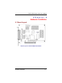
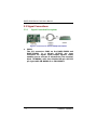
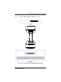
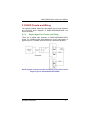
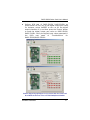
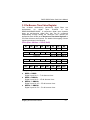
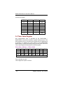
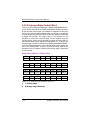
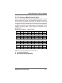
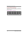
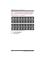
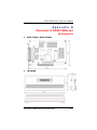
DASP-52056/DASP-52056L Isolated 32 D/I and 24 D/O Card User’s Manual Disclaimers The information in this manual has been carefully checked and is believed to be accurate. Axiomtek Co., Ltd. assumes no responsibility for any infringements of patents or other rights of third parties which may result from its use. Axiomtek assumes no responsibility for any inaccuracies that may be contained in this document. Axiomtek makes no commitment to update or to keep current the information contained in this manual. Axiomtek reserves the right to make improvements to this document and/or product at any time and without notice. No part of this document may be reproduced, stored in a retrieval system, or transmitted, in any form or by any means, electronic, mechanical, photocopying, recording, or otherwise, without the prior written permission of Axiomtek Co., Ltd. Copyright 2004 by Axiomtek Co., Ltd. All rights reserved. September 2004, Version A1.0 Printed in Taiwan ii ESD Precautions Integrated circuits on computer boards are sensitive to static electricity. To avoid damaging chips from electrostatic discharge, observe the following precautions: Do not remove boards or integrated circuits from their anti-static packaging until you are ready to install them. Before handling a board or integrated circuit, touch an unpainted portion of the system unit chassis for a few seconds. This helps to discharge any static electricity on your body. Wear a wrist-grounding strap, available from most electronic component stores, when handling boards and components. Trademarks Acknowledgments AXIOMTEK is a trademark of Axiomtek Co., Ltd. IBM is a registered trademark of International Business Machines Corporation. MS-DOS, and Windows 95/98/NT/2000 are trademarks of Microsoft Corporation. Phoenix-Award is a trademark of Phoenix-Award Software, Inc. IBM, PC/AT, PS/2, VGA are trademarks of International Business Machines Corporation. Intel and Celeron, Pentium III are trademarks of Intel Corporation. Other brand names and trademarks are the properties and registered brands of their respective owners. iii Table of Contents Chapter 1 1.1 1.2 1.3 Chapter 2 2.1 2.2 Introduction.....................................................1 Features ...................................................................2 Specifications..........................................................2 Accessories .............................................................4 Hardware Installation ...................................5 Board Layout ...........................................................5 Signal Connections.................................................6 2.2.1 Signal Connection Descriptions ..............................6 2.2.2 Digital Input/Output Connector CON1 ....................7 2.3 DI/DO Circuits and Wiring ......................................9 2.3.1 Digital Input Port Circuits and Wiring ....................9 2.3.2 Digital Output Port Circuits and Wiring ................ 10 2.4 Quick Setup and Test ...........................................11 Chapter 3 3.1 3.2 3.3 3.4 3.5 3.6 3.7 3.8 3.9 3.10 Registry Structure and Format...................19 Overview ................................................................19 Digital Input Registers ..........................................20 De-Bounce Time Value Register..........................21 Timer Value Register ............................................22 Timer Interrupt Control Word...............................23 I/O Interrupt Edge Control Word..........................24 I/O Interrupt Mask Control Word..........................25 Clear Output Control Word ..................................26 Digital Output Register .........................................27 I/O Interrupt Clear and Status Register.............28 Appendix A Dimension of DASP-52056 and Accessories ..........................................................................29 iv DASP-52056 Series Card User’s Manual C h a p t e r 1 Introduction The DASP-52056 is a PCI-bus, 32 isolated D/I and 24 isolated D/O card. It offers 2K bytes on-board battery backup RAM to solve users' problem that they used not to effectively protect important data while the system shuts down. The DASP-52056 is also fitted with one programmable timer interrupt and an I/O interrupt. On-board Battery Backup RAM The design, on-board battery backup RAM, supports a storage unit that data can remain stored safely without the risk of losing it, and assures data security while the PC shuts down or loses power. While working on it, users can save important data or key parameters in advance or constantly update and save output values in RAM that lets users always obtain the latest figures, or furthermore, save multiple data. Introduction 1 DASP-52056 Series Card User’s Manual 1.1 Features 32 isolated digital inputs for source type 32 interrupt input I/O (digital input), 24 isolated digital outputs for sink type 2K battery backup RAM for backup nonvolatile data (only for DASP-52056) One programmable timer and interrupt Supports Windows® 98/NT/2000/XP, Labview 6.0/7.0 driver Supports VB, VC, BCB, Delphi sample program 1.2 Specifications Isolated Digital Inputs Input channels: 32 Interrupt input channel: 32 Interrupt input source type: I/O interrupt & timer interrupt Input type: source Optical isolated: 2500VDC Opto-isolator response time: 20us Over-voltage protect: 50VDC, Input voltage: VIH (max.) 36VDC VIH (min.) 4VDC VIL (max.) 3VDC Input Current: 10 VDC 2.9mA (typical) 12 VDC 3.6mA (typical) 24 VDC 7.5mA (typical) 36 VDC 11.5mA (typical) 2 Introduction DASP-52056 Series Card User’s Manual Isolated Digital Outputs Output channels: 24 Output type: sink (open collector) Optical Isolation: 2500VDC Output voltage: 10 ~ 40 VDC Opto-isolator response time: 20us Sink current: 100 mA max./channel Battery Backup RAM (DASP-52056 only) Range of base address: P&P memory mapped Size: 2K bytes Programmable Interval Timer Channel: 1 Resolution: 32 bits Time base: 2MHz Timer range: 0.5s~2147ms General Environment I/O connector type 68-pin SCSI-II pin type female Power consumption Typical: +5 V @ 300mA, Max. +5 V @ 500mA Temperature Operation: 0 ~ 60°C, Storage -20 ~ 70°C Relative humidity: 0 to 90% non-condensing Dimensions: 185mm x 122mm Introduction 3 DASP-52056 Series Card User’s Manual 1.3 Accessories To make the DASP-52056/DASP-52056L functionality complete, we carry a versatility of accessories for different user’s requirements in the following items: Cable CB-89268-2: 68-pin SCSI-II pin type male with 2m length CB-89268-5: 68-pin SCSI-II pin type male with 5m length Terminal Board TB-88268: 68-pin SCSI-II terminal block with DIN-rail mounting The terminal block is directly connected to I/O connector CON1 of the DASP-52056/ DASP-52056L. 4 Introduction DASP-52056 Series Card User’s Manual C h a p t e r 2 Hardware Installation 2.1 Board Layout Board Layout for DASP-52056/DASP-52056L Hardware Installation 5 DASP-52056 Series Card User’s Manual 2.2 Signal Connections 2.2.1 Signal Connection Descriptions Signal Connections for DASP-52056/DASP-52056L CON1: The I/O connector CON1 on the DASP-52056 and DASP-52056L is a 68-pin SCSI-II pin type connector for digital input/output signals. CON1 enables you to connect to accessories, the terminal block TB-88268, with the shielded 68-pin SCSI-II pin type cable CB-89268-2 or CB-89268-5. 6 Hardware Installation DASP-52056 Series Card User’s Manual 2.2.2 Digital Input/Output Connector CON1 CON1 CB-89268 TB-88268 DIO Signal Connections for DASP-52056/DASP-52056L Hardware Installation 7 DASP-52056 Series Card User’s Manual The pin assignment of CON1 of DASP-52056 is listed as follows. Pin 68 67 66 65 64 63 62 61 60 59 58 57 56 55 54 53 52 51 50 49 48 47 46 45 44 43 42 41 40 39 38 37 36 35 8 Description GND GND GND DI31 DI29 DI27 DI25 DI23 DI21 DI19 DI17 DI15 DI13 DI11 DI9 DI7 DI5 DI3 DI1 DOUT23 DOUT21 DOUT19 DOUT17 DOUT15 DOUT13 DOUT11 DOUT9 DOUT7 DOUT5 DOUT3 DOUT1 ICOM+ ICOM+ ICOM+ Pin 34 33 32 31 30 29 28 27 26 25 24 23 22 21 20 19 18 17 16 15 14 13 12 11 10 9 8 7 6 5 4 3 2 1 Description GND GND GND DI30 DI28 DI26 DI24 DI22 DI20 DI18 DI16 DI14 DI12 DI10 DI8 DI6 DI4 DI2 DI0 DOUT22 DOUT20 DOUT18 DOUT16 DOUT14 DOUT12 DOUT10 DOUT8 DOUT6 DOUT4 DOUT2 DOUT0 ICOM+ ICOM+ ICOM+ 68 34 35 1 Hardware Installation DASP-52056 Series Card User’s Manual 2.3 DI/DO Circuits and Wiring The optically isolated digital input and digital output wiring diagrams and functional block diagrams of DASP-52056/DASP-5205L are shown as follows. 2.3.1 Digital Input Port Circuits and Wiring There are 32 digital input channels on DASP-52056/DASP-5205L board. The following figure demonstrates the circuit configuration of digital input port. The basic layout and wiring is presented as below. Block Diagram of Internal Circuits and Wiring of Optically Isolated Digital Input for DASP-52056/DASP-52056L Hardware Installation 9 DASP-52056 Series Card User’s Manual 2.3.2 Digital Output Port Circuits and Wiring There are 24 digital output channels on DASP-52056/ DASP-52056L board. The digital output port is sink type (open-collector). The following figure demonstrates the circuit configuration. The basic layout is presented as below. OCOM+ DOUT0 Load 24VDC Photocopler DOUT23 Load GND Block Diagram of Internal Circuits and Wiring of Isolated Digital Output for DASP-52056/DASP-52056L 10 Hardware Installation DASP-52056 Series Card User’s Manual 2.4 Quick Setup and Test To install a new DASP-52056/DASP-52056L into an IBM PC compatible computer, at first, power-off the PC and open its chassis, then plug the DASP-52056/DASP-52056L into a PCI slot of mother-board of the PC. The DASP-52056/DASP-52056L is a plug and play device for MS Windows, and the OS will detect your DASP-52056/DASP-52056L after you power on the PC. The detail of driver and software installation is described in software manual of DASP-52056/DASP-52056L. After the hardware and software installation, user can emulate and test DASP-52056/DASP-52056L step by step as follows. To perform a complete test of DASP-52056 / DASP-52056L, we can route the output channels to the input channels of DASP-52056 / DASP-52056L directly for read-back. And then, by following the DASP-52056 /DASP-52056L test branch of the ToolWorkShop which will fully test all the digital I/O channels of the DASP-52056/DASP-52056L as descried in the following paragraphs. Launch the ‘PCI Configuration Utility’ of DASP-52000 series to ensure that the resource of DASP-52056 / DASP-52056L is properly dispatched by the OS. Press the scan button in the toolbar of the ‘PCI Configuration Utility’ to find the installed DASP-52056/DASP-52056L, and then check the resource list. Scan DASP-52056/DASP-52056L with PCI Configuration Utility and Check the Dispatched Resource Hardware Installation 11 DASP-52056 Series Card User’s Manual Exit the ‘PCI Configuration Utility’ and launch the ‘ToolWorkShop’ for DASP-52056 / DASP-52056L. Select DASP-52056 / DASP-52056L as the test target shown as follows. Launch ToolWorkShop Select Board Test 12 Hardware Installation DASP-52056 Series Card User’s Manual Select test target: DASP52056/ DASP52056L Hardware Installation 13 DASP-52056 Series Card User’s Manual Perform DIO test of DASP-52056/ DASP-52056L as shown above. At first, check the device information and press ‘Enable’ button to load DASP-52056/DASP-52056L library shown in following. Check Device Information and Press ‘Setup’ Button to Load DASP-52056/DASP-52056L library 14 Hardware Installation DASP-52056 Series Card User’s Manual Perform DIO test of DASP-52056/ DASP-52056L as shown below. At first, key in the digital output port value, for instance, writes 0x0ffffff to turn on all the digital output channels of it, and then press the ‘Output’ button to send the digital output port value to DASP-52056/ DASP 52056L. Verify the digital input value presented in for the DI/O test panel of ‘TOOLWORKSHOP’ DASP-52056/DASP-52056L. Perform Digital Input/Output Test by Set the DO Port Value and Read Back the DI Port Value of DASP-52056/DASP-52056L Hardware Installation 15 DASP-52056 Series Card User’s Manual Perform the Interrupt Test by selecting the Interrupt Test Page in ‘TOOLWORKSHOP’. At first, key in the Tick value (1~65535) and press ‘Set ‘ Button to update the Timer Configuration. Press the ‘Start‘ Button to start the timer interrupt and the ISR Count will count up. The count will stop when the ‘Stop‘ button is pressed. The Interrupt testing page is as shown below. Perform Interrupt Test by Set the Tick Value and Start/Stop Timer Interrupt of DASP-52056/DASP-52056L 16 Hardware Installation DASP-52056 Series Card User’s Manual DIO and SRAM (only supported by DASP-52056) can be auto-tested in this page, as shown below. The Error count shows the times of testing failure. Press Start button to start auto testing and press Stop to stop. The DIO connection must be wired as the following configuration to prevent the testing failure, DI [0~7] DI [8~15] DI [16~23] DI [24~31] ⇔ ⇔ ⇔ ⇔ DO [0~7] DO [8~15] DO [16~23] DO [0~7] Perform the DIO and SRAM Auto Test on DASP-52056 Hardware Installation 17 DASP-52056 Series Card User’s Manual Perform the battery-backup RAM test of DASP-52056 as shown below. At first, key in the address offset of battery-backup RAM to test in the ‘Offset’ field, for instance, writes 0x0 to test the first byte of battery-backup RAM of the DASP-52056, and key in the byte value to the ‘Write’ field and press the ‘Write’ button to write the byte value to DASP-52056. To verify the byte value write to the specified address of battery-backup RAM of DASP-52056, press the ‘Read’ button of SRAM test panel of the ‘ToolWorkShop’. Perform Battery-Backup RAM Test by Set the Byte Address and Byte Value to Write and Read Back the Byte Value from the Battery-Backup RAM of DASP-52056 Before exiting ‘ToolWorkShop’, press ‘Release’ button to release DASP-52056/DASP-52056L library. 18 Hardware Installation DASP-52056 Series Card User’s Manual C h a p t e r 3 Register Structure and Format 3.1 Overview The DASP-52056/DASP-52056L occupies 24 consecutive I/O addresses. The address of each register is defined as the board’s base address plus an offset. The I/O registers and their corresponding functions are listed in the followings. Address Base + 0x00 Base + 0x04 Base + 0x08 Base + 0x0C Read Digital Input (32 bits) Reserved Reserved Reserved Base + 0x10 Reserved Base + 0x14 Base + 0x18 Base + 0x1C Reserved Reserved Reserved I/O Interrupt Clear and Status Base + 0x20 Registry Structure and Format Write Reserved De-bounce Time Timer Value Timer Interrupt Control I/O Interrupt Edge Control I/O Interrupt Mask Clear Output Digital Output (24 bits) Reserved 19 DASP-52056 Series Card User’s Manual 3.2 Digital Input Registers The DASP-52056/DASP-52056L provides 32 optically isolated digital inputs. A double word space is reversed start from offset 0 of I/O address of them. The low word (D0 – D15) of the space latches digital input DI0~DI15, the high word (D16~D31) of the space latches digital input DI16~DI31. The details of bit-mapping of Digital Input Register are shown in the following. Read (Base Address + Offset 0x00) D7 DIN7 D6 DIN6 D5 DIN5 D4 DIN4 D3 DIN3 D2 DIN2 D1 DIN1 D0 DIN0 D15 D14 D13 D12 D11 D10 DIN15 DIN14 DIN13 DIN12 DIN11 DIN10 D9 DIN9 D8 DIN8 D23 D22 D21 D20 D19 D18 D17 D16 DIN23 DIN22 DIN21 DIN20 DIN19 DIN18 DIN17 DIN16 D31 D30 D29 D28 D27 D26 D25 D24 DIN31 DIN30 DIN29 DIN28 DIN27 DIN26 DIN25 DIN24 20 Registry Structure and Format DASP-52056 Series Card User’s Manual 3.3 De-Bounce Time Value Register Four on-board anti-bouncing (de-bounce) digital filters are implemented for digital input channels of the DASP-52056/DASP-52056L. 8 consecutive digital input channels share an anti-bouncing digital filter that can be configured independently through writing the de-bounce time interval (an appropriate clock divider) to the De-bounce Time Value Registers to count the de-bounce time interval. The details of bit-mapping of these registers are shown in the following. Write (Base Address + Offset 0x04) D7 D6 D5 D4 Reserved D3 D2 DBT2 D1 DBT1 D0 DBT0 D15 D14 D13 D12 Reserved D11 D10 D9 DBT10 DBT9 D8 DBT8 D23 D22 D21 D20 Reserved D19 D18 D17 D16 DBT18 DBT17 DBT16 D31 D30 D29 D28 Reserved D27 D26 D25 D24 DBT26 DBT25 DBT24 Setting this register to avoid input contact-bounce. DBT0 ~ DBV2: Digital input bit 0 ~ 7 de-bounce time. DBT8 ~ DBV10: Digital input bit 8 ~ 15 de-bounce time. DBT16 ~ DBV18: Digital input bit 16 ~ 23 de-bounce time. DBT24 ~ DBV26: Digital input bit 24 ~ 31 de-bounce time. Registry Structure and Format 21 DASP-52056 Series Card User’s Manual Clock source: 4MHZ DBTn-2 0 0 0 0 1 1 1 1 DBTn-1 0 0 1 1 0 0 1 1 DBTn 0 1 0 1 0 1 0 1 Divider 32 64 128 256 512 1024 2048 4096 3.4 Timer Value Register One programmable timer is provided by the DASP-52056 / DASP-52056L, and can be served as a system interrupt source. The timer resolution is 0.5µs, and the timer interval can be configured up to 2147ms. To configure the timer interval of the DASP-52056/ DASP-52056L is simply achieved by writing a 32 bits timer value to its Timer Value Register as described in the following table. Write (Base Address + Offset 0x08) D7 D15 D23 D31 D6 D14 D22 D30 D5 D13 D21 D29 D4 D3 D12 D11 D20 D19 D28 D27 32 bits timer value D2 D10 D18 D26 D1 D9 D17 D25 D0 D8 D16 D24 Timer resolution is 0.5µs. Timer range from 0.5µs to 2147ms. 22 Registry Structure and Format DASP-52056 Series Card User’s Manual 3.5 Timer Interrupt Control Word To operate the on-board timer of the DASP-52056/DASP-52056L as an interrupt source, user can write the corresponding bit (D0) of its Timer Interrupt Control Register a low (0) to enable the timer interrupt, the presents of a high (1) at D0 of the Timer Interrupt Control Register will disable the interrupt. Write (Base Address + Offset 0x0C) D7 D6 D5 D4 D3 Reserved D2 D1 D0 EnTINT D15 D23 D31 D14 D22 D30 D13 D21 D29 D12 D11 D20 D19 D28 D27 Reserved D10 D18 D26 D9 D17 D25 D8 D16 D24 EnTINT: Timer Interrupt Control Bit 0: Enable 1: Disable (Default) Registry Structure and Format 23 DASP-52056 Series Card User’s Manual 3.6 I/O Interrupt Edge Control Word There is an I/O interrupt provided by the DASP-52056/DASP-52056L. All the 32 D/I channels of the DASP-52056/DASP-52056L can serve as the interrupt source signal, and multiple D/I channels can serve as the interrupt source signals simultaneously. An OR-logic is introduced to solve the I/O interrupt status when multiple D/I channels is selected to trigger the interrupt. The trigger edge of I/O interrupt can be assigned by writing the Interrupt Edge Control Register, and the interrupt source signal can be selected by writing the mask value to the Interrupt Mask Control Register as described in 3.7. To assign the interrupt edge of each D/I channel of the DASP-52056/DASP-52056L, write the corresponding bits of the interrupt edge control register as lists in the following table. A high bit (1) denotes falling edge will be detected for the D/I channel, otherwise, the raising edge is monitoring for that channel. Read (Base Address + Offset 0x10) D7 D6 D5 D4 D3 D2 D1 D0 EDG7 EDG6 EDG5 EDG4 EDG3 EDG2 EDG1 EDG0 D15 D14 D13 D12 D11 D10 D9 D8 EDG15 EDG14 EDG13 EDG12 EDG11 EDG10 EDG9 EDG8 D23 D22 D21 D20 D19 D18 D17 D16 EDG23 EDG22 EDG21 EDG20 EDG19 EDG18 EDG17 EDG16 D31 D30 D29 D28 D27 D26 D25 D24 EDG31 EDG30 EDG29 EDG28 EDG27 EDG26 EDG25 EDG24 EDG0-31: IO Interrupt Edge Control Bit (I/O 0-31) 1: Falling edge 0: Rising edge (Default) 24 Registry Structure and Format DASP-52056 Series Card User’s Manual 3.7 I/O Interrupt Mask Control Word All the 32 D/I channels of the DASP-52056/DASP-52056L can serve as the interrupt source signal, and multiple D/I channels can serve as the interrupt source signals simultaneously. An OR-logic is introduced to solve the I/O interrupt status when multiple D/I channels is selected to trigger the interrupt. The interrupt source signal can be selected by writing the mask value to the Interrupt Mask Control Register. The bit mapping of Interrupt Mask Control Register is described in the following table. Read (Base Address + Offset 0x14) D7 D6 D5 D4 D3 D2 D1 D0 MSK7 MSK6 MSK5 MSK4 MSK3 MSK2 MSK1 MSK0 D15 D14 D13 D12 D11 D10 D9 D8 MSK15 MSK14 MSK13 MSK12 MSK11 MSK10 MSK9 MSK8 D23 D22 D21 D20 D19 D18 D17 D16 MSK23 MSK22 MSK21 MSK20 MSK19 MSK18 MSK17 MSK16 D31 D30 D29 D28 D27 D26 D25 D24 MSK31 MSK30 MSK29 MSK28 MSK27 MSK26 MSK25 MSK24 MSK0-31: IO Interrupt Mask Control Bit (I/O 0-31) 1: Enable (Unmask) 0: Disable (Mask) (Default) Registry Structure and Format 25 DASP-52056 Series Card User’s Manual 3.8 Clear Output Control Word A global clear to all of the D/O channels of the DASP-52056 / DASP-52056L can be achieved by performing a write to the Clear Output Control Register. Write (Base Address + Offset 0x18) D7 D15 D23 D31 26 D6 D5 D4 D3 D2 D1 D14 D13 D12 D11 D10 D9 D22 D21 D20 D19 D18 D17 D30 D29 D28 D27 D26 D25 Write Any Value to Clear All Digital Output Bits to 0 D0 D8 D16 D24 Registry Structure and Format DASP-52056 Series Card User’s Manual 3.9 Digital Output Register The DASP-52056/DASP-52056L provides 24 optically isolated digital output channels. A double word space is reversed start from offset 0x1C of I/O address of them. The low word (D0 – D15) of the space latches digital output value DO0~DO15, and part of the high word (D16~D23) of the space latches digital output value DO16~DO23. The details of bit-mapping of Digital Output Register are shown in the following. Write (Base Address + Offset 0x1C) D7 D6 D5 D4 D3 D2 D1 D0 DOUT7 DOUT6 DOUT5 DOUT4 DOUT3 DOUT2 DOUT1 DOUT0 D15 D14 D13 D12 D11 D10 D9 D8 DOUT DOUT DOUT DOUT DOUT DOUT DOUT9 DOUT8 15 14 13 12 11 10 D23 D22 D21 D20 D19 D18 D17 D16 DOUT DOUT DOUT DOUT DOUT DOUT DOUT DOUT 23 22 21 20 19 18 17 16 D31 D30 D29 D28 D27 Reserved Registry Structure and Format D26 D25 D24 27 DASP-52056 Series Card User’s Manual 3.10 I/O Interrupt Clear and Status Register Read this register to read in IO interrupt status and clear interrupt. Read (Base Address + Offset 0x20) D7 IDIN7 D6 IDIN6 D5 IDIN5 D4 IDIN4 D3 IDIN3 D2 IDIN2 D1 IDIN1 D0 IDIN0 D15 D14 D13 D12 D11 D10 D9 IDIN15 IDIN14 IDIN13 IDIN12 IDIN11 IDIN10 IDIN9 D8 IDIN8 D23 D22 D21 D20 D19 D18 D17 D16 IDIN23 IDIN22 IDIN21 IDIN20 IDIN19 IDIN18 IDIN17 IDIN16 D31 D30 D29 D28 D27 D26 D25 D24 IDIN31 IDIN30 IDIN29 IDIN28 IDIN27 IDIN26 IDIN25 IDIN24 IDIN0-31: IO Interrupt Status Bit (I/O 0-31) 1: Interrupt happens 0: No Interrupt 28 Registry Structure and Format DASP-52056 Series Card User’s Manual Appendix A Dimension of DASP-52056 and Accessories DASP-52056/ DASP-52056L TB-88268 Dimension of DASP-52056 and Accessories 29